Magnetic microscopy of domains and domain walls in ...
228
HAL Id: tel-01743840 https://tel.archives-ouvertes.fr/tel-01743840 Submitted on 26 Mar 2018 HAL is a multi-disciplinary open access archive for the deposit and dissemination of sci- entific research documents, whether they are pub- lished or not. The documents may come from teaching and research institutions in France or abroad, or from public or private research centers. L’archive ouverte pluridisciplinaire HAL, est destinée au dépôt et à la diffusion de documents scientifiques de niveau recherche, publiés ou non, émanant des établissements d’enseignement et de recherche français ou étrangers, des laboratoires publics ou privés. Magnetic microscopy of domains and domain walls in ferromagnetic nanotubes Michal Staňo To cite this version: Michal Staňo. Magnetic microscopy of domains and domain walls in ferromagnetic nanotubes. Mate- rials Science [cond-mat.mtrl-sci]. Université Grenoble Alpes, 2017. English. NNT : 2017GREAY063. tel-01743840
-
Upload
khangminh22 -
Category
Documents
-
view
2 -
download
0
Transcript of Magnetic microscopy of domains and domain walls in ...
HAL Id: tel-01743840https://tel.archives-ouvertes.fr/tel-01743840
Submitted on 26 Mar 2018
HAL is a multi-disciplinary open accessarchive for the deposit and dissemination of sci-entific research documents, whether they are pub-lished or not. The documents may come fromteaching and research institutions in France orabroad, or from public or private research centers.
L’archive ouverte pluridisciplinaire HAL, estdestinée au dépôt et à la diffusion de documentsscientifiques de niveau recherche, publiés ou non,émanant des établissements d’enseignement et derecherche français ou étrangers, des laboratoirespublics ou privés.
Magnetic microscopy of domains and domain walls inferromagnetic nanotubes
Michal Staňo
To cite this version:Michal Staňo. Magnetic microscopy of domains and domain walls in ferromagnetic nanotubes. Mate-rials Science [cond-mat.mtrl-sci]. Université Grenoble Alpes, 2017. English. �NNT : 2017GREAY063�.�tel-01743840�

THÈSEPour obtenir le grade de
DOCTEUR DE LA COMMUNAUTÉ UNIVERSITÉ GRENOBLE ALPESSpécialité : Nanophysique
Arrêté ministériel : 25 mai 2016
Présentée par
Michal STAŇO
Thèse dirigée par Dr. Olivier FRUCHART, SPINTEC, Grenoble
préparée au sein du CNRS, Institut Néel dans l'École Doctorale de Physique
Microscopie des domaines etparois de domaines dans lesnanotubes ferromagnétiques
Thèse soutenue publiquement le 3 octobre 2017,devant le jury composé de :
Dr. Riccardo HERTELDirecteur de recherche CNRS, IPCMS, Strasbourg RapporteurProf. Hans-Josef HUGProfesseur des universités, University of Basel, Basel RapporteurDirecteur de laboratoire, EMPA, DübendorfDr. Claire BARADUCIngénieur-chercheuse, SPINTEC, Grenoble ExaminatriceDr. Bénédicte WAROT-FONROSEChargée de recherche CNRS, CEMES, Toulouse ExaminatriceDr. Stefania PIZZINIDirectrice de recherche CNRS, Institut Néel, Grenoble Présidente

THÈSEPour obtenir le grade de
DOCTEUR DE LA COMMUNAUTÉ UNIVERSITÉ GRENOBLE ALPESSpécialité : Nanophysique
Arrêté ministériel : 25 mai 2016
Présentée par
Michal STAŇO
Thèse dirigée par Dr. Olivier FRUCHART, SPINTEC, Grenoble
préparée au sein du CNRS, Institut Néel dans l'École Doctorale de Physique
Magnetic microscopy ofdomains and domain walls in
ferromagnetic nanotubes
Thèse soutenue publiquement le 3 octobre 2017,devant le jury composé de :
Dr. Riccardo HERTELDirecteur de recherche CNRS, IPCMS, Strasbourg RapporteurProf. Hans-Josef HUGProfesseur des universités, University of Basel, Basel RapporteurDirecteur de laboratoire, EMPA, DübendorfDr. Claire BARADUCIngénieur-chercheuse, SPINTEC, Grenoble ExaminatriceDr. Bénédicte WAROT-FONROSEChargée de recherche CNRS, CEMES, Toulouse ExaminatriceDr. Stefania PIZZINIDirectrice de recherche CNRS, Institut Néel, Grenoble Présidente

ABSTRACTThis thesis explores magnetic configurations, namely magnetic domains and domain walls(DWs) in single ferromagnetic metallic nanotubes (diameters 50–400 nm) by means of magneticmicroscopies and numerical modelling. The work benefited from international collaborationwith TU Darmstadt (synthesis), synchrotrons Elettra and Soleil as well as CNRS CEMES(magnetic imaging). Using electrochemical methods and nanoporous templates, we couldfabricate Ni, NiCo, CoNiB, and NiFeB nanotubes as well as Ni wire-tube elements. For theimaging, we relied mainly on X-ray Magnetic Circular Dichroism coupled with PhotoEmissionElectron Microscopy (XMCD-PEEM). We show the first experimental microscopy images ofmagnetic domains in metallic nanotubes. In long (30 µm) CoNiB tubes, we observed manyazimuthal (flux-closure) magnetic domains separated by very narrow DWs. This is in contrastwith literature and recent experiments where only axial domains appeared for similar geometry.By annealing, changing the chemical composition or just decreasing the nanotube diameter wecould obtain also the axial domains. Therefore, tubes are versatile as magnetic domains can beprepared almost à la carte. We demonstrated switching of both axial and azimuthal domainswith a magnetic field. We imaged also multilayered tubes – an equivalent of multilayeredflat films that form a basic brick of current spintronics. We obtained two magnetic layers(exchange-) decoupled by an oxide spacer. Such a first-of-its-kind structure and its imagingpaves the way towards 3D spintronics and magnetism based on vertical arrays of tubes.
KEYWORDSMagnetic nanotube, micromagnetism, domain wall, XMCD-PEEM, electron holography, elec-trochemistry
RESUMÉCette thèse explore les domaines magnétiques et les parois de domaine (PD), dans des nan-otubes (NTs) métalliques ferromagnétiques individuels (diamètres 50-400 nm) au moyen demicroscopies magnétiques et de modélisation numérique. Le travail a bénéficié d’une collab-oration internationale avec TU Darmstadt (synthèse), les synchrotrons Elettra et Soleil ainsique CNRS CEMES (imagerie magnétique). En utilisant des méthodes électrochimiques et desgabarits nanoporeux, nous avons fabriqué des NTs de Ni, NiCo, CoNiB et NiFeB ainsi que deséléments fil-tube de Ni. Pour l’imagerie, nous utilisons principalement le dichroïsme circulairemagnétique de rayons X associé à la microscopie à émission de photoelectrons (XMCD-PEEM).Nous avons réalisé les premières images microscopiques de domaines magnétiques dans les NTs.Dans des tubes CoNiB longs (30 µm), nous avons observé un grand nombre de domaines az-imutaux séparés par des PD très étroites. Cela contraste avec la littérature et les expériencesrécentes où seuls des domaines axiaux apparaissent pour une géométrie similaire. Par re-cuit, en changeant la composition chimique ou simplement en diminuant le diamètre des NTs,nous avons également pu obtenir les domaines axiaux – préparation des domaines presque àla carte. Nous avons démontré le renversement des domaines axiaux et azimutaux avec unchamp magnétique. En vue d’ouvrir la voie à des tubes multicouches - un équivalent de filmsplats multicouches qui forment une brique de base de la spintronique actuelle, nous avonsobtenu deux couches magnétiques découplées par un intercalaire d’oxyde. Ces structures etleurs imagerie ouvrent la voie à la spintronique 3D basée sur des réseaux de tubes verticaux.
MOTS CLÉSNanotube magnétique, micromagnétisme, paroi de domaine, XMCD-PEEM, holographie élec-tronique, électrochimie

ACKNOWLEDGEMENT
First of all, I thank Sandra Schaefer for a great collaboration, preparation of very good samples,information on electroless plating and polymeric membranes. Without her contribution thepresented work would be much thinner. Last but not least, I appreciate nice stamps on theparcels with samples. Further, I acknowledge my supervisor, Olivier Fruchart, for giving memany nice (and challenging) opportunities as well as supplying means for their realization. Iam grateful to Dr. Ricardo Hertel and Prof. Hans-Josef Hug for accepting to be referees ofmy work and reading through the (intricate) manuscript. Further I appreciate the commentsand notes of other jury members: Claire Baraduc, Bénédicte Warrot-Fonrose, and StefaniaPizzini.
Great thanks goes to my colleagues from Institut Néel and Spintec. It is not possible to men-tion all of them, therefore I apologize to those who are not listed below. I thank to MárlioBonfim and Jan Vogel for help with the focused MOKE setup, Ségolène Jamet for discussionson simulations and XMCD-PEEM simulation code, Daria Gusakova for unroll-tube script anddiscussion on micromagnetic simulations, Jean-Christophe Toussaint for development of sim-ulation codes, Laurent Cagnon for transmission electron microscopy and some tips regarding(electro)chemistry, and Alexis Wartelle for numerous discussions and help not only with livingin France. I am grateful to Nanofab (namely Bruno Fernandez and Jean-Francois Motte) andOptics and Microscopy (Simon Le Denmat, Sebastien Pairis) technological groups for theirsupport and help with microfabrication (substrates, sample processing) and characterization(AFM, SEM), respectively; Cécile Nemiche for express printing of all the posters and the thesis.
Conducting the research would be impossible without occasional relax, Grenoble mountains,board games in K fée des jeux (avec fondant au chocolat), good meals in H2 restaurant,and support of my family in previous education and stages of life. I express my gratitudeto Karol Nogajevski for being such a good mountain guide; the trip squads for nice hikes. Iappreciate also help of my friends and colleagues from Brno: Viola Křižáková for coffee breaks,slack-line, discussions, very precise manuscript corrections and teaching me (reminding me of)some English rules. I highly appreciate a car power transformer (DC to AC) provided by LukášFlajšman enabling me to proceed with the manuscript during our trip in Canada (CanadianRockies).
I am gratefull to Elettra and Soleil synchrotron facilities for allocating beamtime for theXPEEM and STXM experiments. A special thanks goes to Grande Onur and Grande An-drea, Bazovicca Center Hotel staff (soups) and Pizzeria Karis/Pesek. Scanning transmissionelectron microscopy microscopy was performed by Eric Gautier at Plateforme de Nanocaractéri-sation PFNC at CEA/Minatec (Grenoble). Electron holography experiments were conductedvia the French research federation METSA with financial support from the CNRS-CEA METSAFrench network (FR CNRS 3507) on the CEMES Toulouse platform. I gratefully acknowledgePhD grant from the Laboratoire d’excellence LANEF in Grenoble (ANR-10-LABX-51-01). Themanuscript was typeset using author-modified LATEX code based on a template from Brno Uni-versity of Technology.

CONTENTS
1 Introduction 12
I Theoretical background & State of the art 17
2 Magnetism in low dimensions 182.1 Magnetically-ordered materials . . . . . . . . . . . . . . . . . . . . . 182.2 Micromagnetism . . . . . . . . . . . . . . . . . . . . . . . . . . . . . 20
2.2.1 Energies at play . . . . . . . . . . . . . . . . . . . . . . . . . . 212.2.2 Characteristic lengths . . . . . . . . . . . . . . . . . . . . . . 242.2.3 Magnetization dynamics . . . . . . . . . . . . . . . . . . . . . 25
2.3 Magnetic domains and domain walls . . . . . . . . . . . . . . . . . . 262.3.1 Origin of magnetic domains and domain walls . . . . . . . . . 262.3.2 Domain walls in nanostrips . . . . . . . . . . . . . . . . . . . . 272.3.3 Domain walls in cylindrical nanowires . . . . . . . . . . . . . . 282.3.4 Domain wall motion . . . . . . . . . . . . . . . . . . . . . . . 28
3 Magnetic nanotubes 313.1 Magnetic textures . . . . . . . . . . . . . . . . . . . . . . . . . . . . . 31
3.1.1 Magnetization phase diagram . . . . . . . . . . . . . . . . . . 313.1.2 Azimuthal domains . . . . . . . . . . . . . . . . . . . . . . . . 33
3.2 Domain walls in magnetic nanotubes . . . . . . . . . . . . . . . . . . 343.2.1 Domain walls in nanotubes with axial domains . . . . . . . . . 353.2.2 Domain walls in nanotubes with azimuthal domains . . . . . . 37
3.3 Experiments on magnetic nanotubes . . . . . . . . . . . . . . . . . . 383.3.1 Experiments on nanotube arrays . . . . . . . . . . . . . . . . 383.3.2 Experiments on single nanotubes . . . . . . . . . . . . . . . . 40
3.4 Fabrication of magnetic nanotubes . . . . . . . . . . . . . . . . . . . 413.4.1 Lithography . . . . . . . . . . . . . . . . . . . . . . . . . . . . 413.4.2 Electrodeposition . . . . . . . . . . . . . . . . . . . . . . . . . 423.4.3 Electroless deposition . . . . . . . . . . . . . . . . . . . . . . . 423.4.4 Atomic layer deposition . . . . . . . . . . . . . . . . . . . . . 433.4.5 Sol-gel and similar chemical methods . . . . . . . . . . . . . . 433.4.6 Other methods . . . . . . . . . . . . . . . . . . . . . . . . . . 43
3.5 Core-shell structures . . . . . . . . . . . . . . . . . . . . . . . . . . . 443.6 Wire-tube nanoelements . . . . . . . . . . . . . . . . . . . . . . . . . 45
3.6.1 Fabrication of wire-tube elements . . . . . . . . . . . . . . . . 46
3.6.2 Numerical simulations of wire-tube elements . . . . . . . . . . 46
II Methods & Instrumentation 48
4 Fabrication 494.1 Templates . . . . . . . . . . . . . . . . . . . . . . . . . . . . . . . . . 49
4.1.1 Fabrication of templates . . . . . . . . . . . . . . . . . . . . . 494.2 Electrodeposition . . . . . . . . . . . . . . . . . . . . . . . . . . . . . 51
4.2.1 Ni wire-tube elements . . . . . . . . . . . . . . . . . . . . . . 534.2.2 NiCo nanotubes . . . . . . . . . . . . . . . . . . . . . . . . . . 53
4.3 Atomic layer deposition . . . . . . . . . . . . . . . . . . . . . . . . . 544.4 Electroless plating . . . . . . . . . . . . . . . . . . . . . . . . . . . . . 54
4.4.1 Templates . . . . . . . . . . . . . . . . . . . . . . . . . . . . . 554.4.2 Fabrication procedure . . . . . . . . . . . . . . . . . . . . . . 564.4.3 Multilayered tubes . . . . . . . . . . . . . . . . . . . . . . . . 58
4.5 Sample preparation for measurements . . . . . . . . . . . . . . . . . . 59
5 Characterization 615.1 Synchrotron X-ray microscopies . . . . . . . . . . . . . . . . . . . . . 61
5.1.1 X-ray PhotoEmission Electron Microscopy . . . . . . . . . . . 625.1.2 Scanning Transmission X-ray Microscopy . . . . . . . . . . . . 675.1.3 Substrates for synchrotron experiments . . . . . . . . . . . . . 68
5.2 Atomic & Magnetic force microscopy . . . . . . . . . . . . . . . . . . 705.2.1 NT-MDT Ntegra Aura with Px controller . . . . . . . . . . . 705.2.2 HR-MFM Nanoscan . . . . . . . . . . . . . . . . . . . . . . . 705.2.3 Probes . . . . . . . . . . . . . . . . . . . . . . . . . . . . . . . 72
5.3 Electron microscopies . . . . . . . . . . . . . . . . . . . . . . . . . . . 725.3.1 Scanning Electron Microscopy . . . . . . . . . . . . . . . . . . 725.3.2 Transmission Electron Microscopy . . . . . . . . . . . . . . . . 73
5.4 Electron holography . . . . . . . . . . . . . . . . . . . . . . . . . . . 735.4.1 Theoretical background . . . . . . . . . . . . . . . . . . . . . . 745.4.2 Instrumentation & data processing . . . . . . . . . . . . . . . 765.4.3 Samples . . . . . . . . . . . . . . . . . . . . . . . . . . . . . . 775.4.4 Electron holography tutorial on NiCo nanowires . . . . . . . . 79
5.5 Magnetometry . . . . . . . . . . . . . . . . . . . . . . . . . . . . . . . 825.5.1 VSM-SQUID . . . . . . . . . . . . . . . . . . . . . . . . . . . 825.5.2 Magneto-optics with focused laser beam . . . . . . . . . . . . 82

6 Simulations 846.1 Micromagnetics . . . . . . . . . . . . . . . . . . . . . . . . . . . . . . 846.2 Object Oriented MicroMagnetic Framework . . . . . . . . . . . . . . 846.3 FeeLLGood . . . . . . . . . . . . . . . . . . . . . . . . . . . . . . . . 85
6.3.1 Geometry and meshing . . . . . . . . . . . . . . . . . . . . . . 856.3.2 Initial magnetic configuration . . . . . . . . . . . . . . . . . . 866.3.3 Post-processing codes . . . . . . . . . . . . . . . . . . . . . . . 87
6.4 Electron-holography code . . . . . . . . . . . . . . . . . . . . . . . . . 886.4.1 NiCo nanowires . . . . . . . . . . . . . . . . . . . . . . . . . . 896.4.2 Tubes . . . . . . . . . . . . . . . . . . . . . . . . . . . . . . . 89
6.5 XMCD-PEEM code . . . . . . . . . . . . . . . . . . . . . . . . . . . . 89
III Results & Discussion – Magnetic nanotubes 91
7 Synthesis of nanotubes 927.1 Electroplating of NiCo nanotubes . . . . . . . . . . . . . . . . . . . . 927.2 Ni twires – wire-tube nanoelements . . . . . . . . . . . . . . . . . . . 95
7.2.1 Electroplating of Ni wire-tube nanoelements . . . . . . . . . . 957.2.2 Further TEM and electron holography on Ni twire . . . . . . . 957.2.3 Summary of twire investigation . . . . . . . . . . . . . . . . . 98
7.3 Electroless depositions at Institut Néel . . . . . . . . . . . . . . . . . 987.4 Summary of nanotube depositions . . . . . . . . . . . . . . . . . . . . 100
8 Domains in CoNiB (nano)tubes 1028.1 Geometry, structure, and chemical composition . . . . . . . . . . . . 1028.2 Azimuthal domains . . . . . . . . . . . . . . . . . . . . . . . . . . . . 1078.3 Magnetic anisotropy . . . . . . . . . . . . . . . . . . . . . . . . . . . 109
8.3.1 Strength of the azimuthal anisotropy . . . . . . . . . . . . . . 1128.3.2 Origin of the azimuthal anisotropy . . . . . . . . . . . . . . . 1188.3.3 Comparison with NiFeB tubes . . . . . . . . . . . . . . . . . . 1208.3.4 Annealing . . . . . . . . . . . . . . . . . . . . . . . . . . . . . 1238.3.5 Sample ageing . . . . . . . . . . . . . . . . . . . . . . . . . . . 126
8.4 Comparison with nanotubes with smaller diameters . . . . . . . . . . 133
9 Domain walls in tubes with azimuthal domains 1359.1 Theoretical considerations . . . . . . . . . . . . . . . . . . . . . . . . 1359.2 Bloch versus Néel walls in magnetic nanotubes . . . . . . . . . . . . . 1359.3 Experimental observation and discussion . . . . . . . . . . . . . . . . 1389.4 Non-zero XMCD-PEEM contrast for the beam "along" the tube axis . 142
IV Results & Discussion – Multilayered nanotubes 145
10 Trilayered tubes: modelling of synthetic ferrimagnets 14710.1 Simulations in OOMMF . . . . . . . . . . . . . . . . . . . . . . . . . 14710.2 Simulations in FeeLLGood . . . . . . . . . . . . . . . . . . . . . . . . 14910.3 Tubular SAF – smaller diameter (50 nm) . . . . . . . . . . . . . . . . 149
10.3.1 Simulated contrast for electron holography . . . . . . . . . . . 15410.4 Tubular SAF – larger diameter (250 nm) . . . . . . . . . . . . . . . . 15410.5 Summary of tubular synthetic ferrimagnet modelling . . . . . . . . . 158
11 Trilayered tubes: experiments 15911.1 Structural and chemical analysis . . . . . . . . . . . . . . . . . . . . . 15911.2 XMCD-PEEM imaging . . . . . . . . . . . . . . . . . . . . . . . . . . 162
11.2.1 Demagnetized state . . . . . . . . . . . . . . . . . . . . . . . . 16211.2.2 Switching by field pulses . . . . . . . . . . . . . . . . . . . . . 16411.2.3 Magnetization switching with quasistatic DC field . . . . . . . 166
11.3 Magnetometry . . . . . . . . . . . . . . . . . . . . . . . . . . . . . . . 16811.4 Annealing and towards synthetic ferrimagnets . . . . . . . . . . . . . 17011.5 Summary of investigation of multilayered tubes . . . . . . . . . . . . 171
12 Conclusion & Perspective 172
Bibliography 178
List of abbreviations 198
List of appendices 200
A How to damage your (nano)tube 201A.1 Nanomachining using AFM . . . . . . . . . . . . . . . . . . . . . . . 201A.2 Laser cutting with micrometric precision . . . . . . . . . . . . . . . . 201A.3 Big task requires big instrument . . . . . . . . . . . . . . . . . . . . 202
B Electron holography 204B.1 Electrostatic interaction constant c𝐸 . . . . . . . . . . . . . . . . . . 204B.2 Electrostatic contribution of a tube . . . . . . . . . . . . . . . . . . . 205B.3 Contrast modelling for domain walls in tubes between azimuthal do-
mains . . . . . . . . . . . . . . . . . . . . . . . . . . . . . . . . . . . 206B.4 Electron holography on NiCo nanowires with modulated diameter . . 208
B.4.1 Domain wall nucleation and displacement . . . . . . . . . . . 208

B.4.2 Domain wall identification . . . . . . . . . . . . . . . . . . . . 210B.4.3 Summary of electron holography on modulated nanowires . . 213
C FeeLLGood – magnetic state initialization 214
D Introduction (Français) 216
E Conclusion (Français) 220

LIST OF FIGURES
1.1 Magnetic racetrack memory . . . . . . . . . . . . . . . . . . . . . . . 121.2 Nanomagnets in 3D and curved geometries . . . . . . . . . . . . . . . 131.3 Specific features of nanotubes: curvature, closed surface, and core-
shell geometry . . . . . . . . . . . . . . . . . . . . . . . . . . . . . . . 152.1 Graphical representation of the LLG equation . . . . . . . . . . . . . 262.2 Influence of energy contributions on a spheroidal particle . . . . . . . 272.3 Scheme of domain walls in nanostrips . . . . . . . . . . . . . . . . . . 282.4 Scheme of domain walls in cylindrical nanowires . . . . . . . . . . . . 292.5 Simulation – domain wall motion in cylindrical wire and nanostrip . . 303.1 Possible magnetization configurations in a tube . . . . . . . . . . . . 313.2 Magnetization phase diagram of a soft magnetic tube . . . . . . . . . 323.3 Investigation of Co nanotubes by Li et al. . . . . . . . . . . . . . . . 343.4 XMCD-PEEM imaging of permalloy tubes with azimuthal magneti-
zation by Wyss et al. . . . . . . . . . . . . . . . . . . . . . . . . . . . 343.5 Scheme of domain walls in nanotubes with axial domains . . . . . . . 353.6 Vortex-like wall velocity under magnetic field for opposite chiralities . 373.7 Scheme of a nanostructure with alternating wire and tube segments . 454.1 Nanoporous membranes . . . . . . . . . . . . . . . . . . . . . . . . . 514.2 Electroplating of tubes in nanopores . . . . . . . . . . . . . . . . . . 524.3 Scheme of radial metal tube growth in a pore . . . . . . . . . . . . . 574.4 Scheme of electroless plating of multilayered tubes . . . . . . . . . . . 584.5 Magnetic tubes on Si substrates with alignment marks . . . . . . . . 605.1 XMCD and X-ray absorption spectroscopy for ferromagnets and their
oxides . . . . . . . . . . . . . . . . . . . . . . . . . . . . . . . . . . . 625.2 Magnetic X-ray microscopies . . . . . . . . . . . . . . . . . . . . . . . 635.3 Shadow XMCD-PEEM scheme . . . . . . . . . . . . . . . . . . . . . 635.4 X-PEEM image with intensity line profile . . . . . . . . . . . . . . . . 645.5 X-PEEM field cartridge: current spike during electromagnet initial-
ization . . . . . . . . . . . . . . . . . . . . . . . . . . . . . . . . . . . 685.6 Si3N4 membranes for STXM . . . . . . . . . . . . . . . . . . . . . . . 695.7 Cantilever resonance – ambient pressure vs low pressure . . . . . . . . 715.8 Scheme of electron holography . . . . . . . . . . . . . . . . . . . . . . 745.9 Nanostructures on TEM grids for electron holography imaging . . . . 795.10 SEM image of a NiCo diameter-modulated nanowire . . . . . . . . . . 805.11 Electron holography of a NiCo nanowire – from hologram to phase map 805.12 Electron holography - opposite magnetization directions in NiCo na-
nowire . . . . . . . . . . . . . . . . . . . . . . . . . . . . . . . . . . . 81

6.1 Effect of mesh smoothing on element size . . . . . . . . . . . . . . . . 877.1 Transmission electron microscopy of electroplated NiCo nanotubes . . 937.2 Transmission electron microscopy – NiCo nanowire vs nanotube . . . 937.3 Magnetic domains in Co-rich NiCo nanowires . . . . . . . . . . . . . 947.4 Nickel twires – transmission electron microscopy . . . . . . . . . . . . 967.5 Electron holography on wire-tube-wire Ni nanostructure . . . . . . . 977.6 Electron microscopy of CoNiB nanotubes from Institut Néel . . . . . 997.7 CoNiB tubes in porous alumina membrane with a pore branching . . 1008.1 Structure of electroless-deposited CoNiB nanotubes (SS53) . . . . . . 1038.2 Chemical analysis of electroless-deposited CoNiB tubes . . . . . . . . 1048.3 X-ray absorption spectroscopy on a CoNiB tube . . . . . . . . . . . . 1068.4 CoNiB tubes with magnetic azimuthal flux-closure domains . . . . . . 1088.5 STXM: circular polarizations and XMCD image . . . . . . . . . . . . 1098.6 Tubular magnetic racetrack memory . . . . . . . . . . . . . . . . . . 1108.7 XMCD-PEEM under external magnetic field . . . . . . . . . . . . . . 1138.8 STXM under external magnetic field . . . . . . . . . . . . . . . . . . 1148.9 Magnetometry on a single tube – magnetooptics with focused laser . 1158.10 Magnetometry on array of CoNiB tubes . . . . . . . . . . . . . . . . 1168.11 Thick CoNiB electroless-deposited film on a Si substrate . . . . . . . 1208.13 Electron holography – NiFeB tube: opposite magnetization directions 1228.14 Electron holography – NiFeB tube after saturation in transverse di-
rection . . . . . . . . . . . . . . . . . . . . . . . . . . . . . . . . . . . 1228.15 Changing magnetic anisotropy of CoNiB tubes upon annealing . . . . 1238.16 Magnetization switching in annealed CoNiB tubes . . . . . . . . . . . 1258.17 Defects upon in-situ annealing of CoNiB tubes . . . . . . . . . . . . . 1258.18 Electron holography phase patterns – CoNiB tube . . . . . . . . . . . 1278.19 Electron holography – magnetic phase maps for a CoNiB tube part . 1288.20 Electron holography – expected magnetic phase for different magnetic
configurations in a tube . . . . . . . . . . . . . . . . . . . . . . . . . 1288.21 Electron holography – another CoNiB tube . . . . . . . . . . . . . . . 1298.22 CoNiB aged tube 1. EFM, MFM, and SEM . . . . . . . . . . . . . . 1318.23 CoNiB aged tube 2. EFM, MFM, and SEM . . . . . . . . . . . . . . 1328.24 CoNiB nanotubes with diameter of 100 nm . . . . . . . . . . . . . . . 1338.25 Magnetic force microscopy of a CoNiB nanotube (diameter 200 nm) . 1349.1 Scheme of domain walls in nanotubes with azimuthal domains . . . . 1369.2 Micromagnetic modelling of Bloch and Néel wall in a tube with two
opposite azimuthal domains . . . . . . . . . . . . . . . . . . . . . . . 1379.3 Unrolled maps of magnetization for domain walls in tubes . . . . . . 1379.4 Micromagnetic simulation of a cross-tie wall in a nanotube . . . . . . 139
9.5 Domain walls between flux-closure domains: experiment vs simulation 1409.6 Simulated XMCD-PEEM contrast for two Bloch walls . . . . . . . . . 1419.7 X-ray beam arriving parallel to tube axis . . . . . . . . . . . . . . . . 1439.8 XMCD-PEEM simulation with beam along tube with Néel wall . . . 1439.9 XMCD-PEEM simulation with beam along solid wire with azimuthal
domains . . . . . . . . . . . . . . . . . . . . . . . . . . . . . . . . . . 14410.1 Tubular SAF in OOMMF . . . . . . . . . . . . . . . . . . . . . . . . 14810.2 Random initial micromagnetic configuration in a tube . . . . . . . . . 15010.3 Small tubular SAF system: random initial magnetization . . . . . . . 15110.4 Small tubular SAF system: antiparallel initial configuration . . . . . 15210.5 Small tubular SAF system: parallel initial configuration . . . . . . . . 15310.6 Tubular SAF: modelling of magnetic phase map for electron holography15510.7 Tubular SAF: larger system . . . . . . . . . . . . . . . . . . . . . . . 15610.8 Magnetic configuration in a single tube . . . . . . . . . . . . . . . . . 15811.1 Multilayered tube with a non-magnetic (oxide) spacer . . . . . . . . . 15911.2 Electron microscopy and chemical imaging of SS148 tubes . . . . . . 16111.3 XMCD-PEEM: NiFeB/SnO𝑥/CoNiB – decoupled magnetic layers . . 16311.4 Images of a SS148 multilayered tube (NiFeB/SnO𝑥/CoNiB) . . . . . . 16311.5 XMCD-PEEM: NiFeB/Pd(incomplete)/CoNiB – coupled magnetic
layers . . . . . . . . . . . . . . . . . . . . . . . . . . . . . . . . . . . . 16411.6 Multilayered tubes: switching of magnetization by field pulses . . . . 16511.7 Multilayered tubes: manipulation of magnetization by DC field . . . . 16711.8 Magnetometry on arrays of multilayered tubes . . . . . . . . . . . . . 169S1 Cutting tubes with atomic force microscopy . . . . . . . . . . . . . . 201S2 Cutting tubes using focused laser beam . . . . . . . . . . . . . . . . . 202S3 Burning well-positioned holes using focused laser beam . . . . . . . . 202S4 Sample affected by electric discharge during XMCD-PEEM measure-
ment . . . . . . . . . . . . . . . . . . . . . . . . . . . . . . . . . . . . 203S1 Dependence of the c𝐸 parameter on electron energy . . . . . . . . . . 205S2 Electrostatic phase contribution for a tube . . . . . . . . . . . . . . . 206S3 Electron holography simulations – domain walls in nanotubes . . . . 207S4 Electron holography simulations – Bloch wall and MIP . . . . . . . . 207S5 NiCo nanowire with pinning sites . . . . . . . . . . . . . . . . . . . . 209S6 Electron holography – NiCo nanowire with a domain wall . . . . . . . 209S7 NiCo nanowire – diameter modulations . . . . . . . . . . . . . . . . . 210S8 Electron holography on NiCo nanowire – experiment vs simulations . 211S9 Electron holography – transverse wall: experiment vs simulation . . . 212S10 Electron holography – simulated phase for different domains walls . . 212

LIST OF TABLES
4.1 Electroless-deposited samples from TU Darmstadt . . . . . . . . . . . 558.1 Saturation magnetostriction 𝜆s for some Co-rich CoNiB compounds. . 12110.1 Summary of simulations of tubular SAF – smaller system . . . . . . . 15010.2 Summary of simulations of tubular SAF – larger system . . . . . . . . 157

1 INTRODUCTION
Research on magnetism in small dimensions (micro and nanomagnetism) has led toa revolution in data storage with high-capacity magnetic recording, e.g. hard diskdrives (HDDs), and to new magnetic sensors (for magnetic field, rotation angle,angular speed), mostly focusing on thin films, nanoparticles and more recently onnanowires.
In 2004 IBM [1] proposed a concept of a non-volatile solid state memory (Fig. 1.1)based on shifting magnetic domain walls (DWs) in magnetic tracks – nanostrips [2].Such memory would be fast, robust (not influenced by power outage, no mechanicallymoving parts), with low power consumption and in case of large arrays of verticaltracks it should provide also high storage density.
Fig. 1.1: Magnetic racetrack memory. The data are stored in magnetic tracks asdomains with opposite magnetization direction. The concept has been demonstratedon a horizontal (planar) strip, but for the high density data storage one would be moreinterested in arrays of vertical tracks containing large number of closely spaced tracks.In ideal case data writing would be done electrically (e.g. with spin-polarized currentto reduce the device consumption). Readout can be accomplished by measuring tunnelmagnetoresistance of a junction connected to the track. Taken from [2].
Recently, also other types of memories (e.g. flash with tens of stacked layers)have gone into 3-dimensional architecture. Even in case of some HDD, there are few(2-3) magnetic recording layers that can be accessed independently [3, 4]. Theseare already on the market or will arrive soon. However, the racetrack memorystill remains in laboratories or better to say as an idea. IBM and many othergroups demonstrated the concept on a planar magnetic strip and contributed tofundamental understanding of domain wall motion in planar strips. However, evenin a recent article [5], Parkin admits that going to 3D is a considerable challenge,mainly from the fabrication point of view. Study of magnetic tracks has focused
12
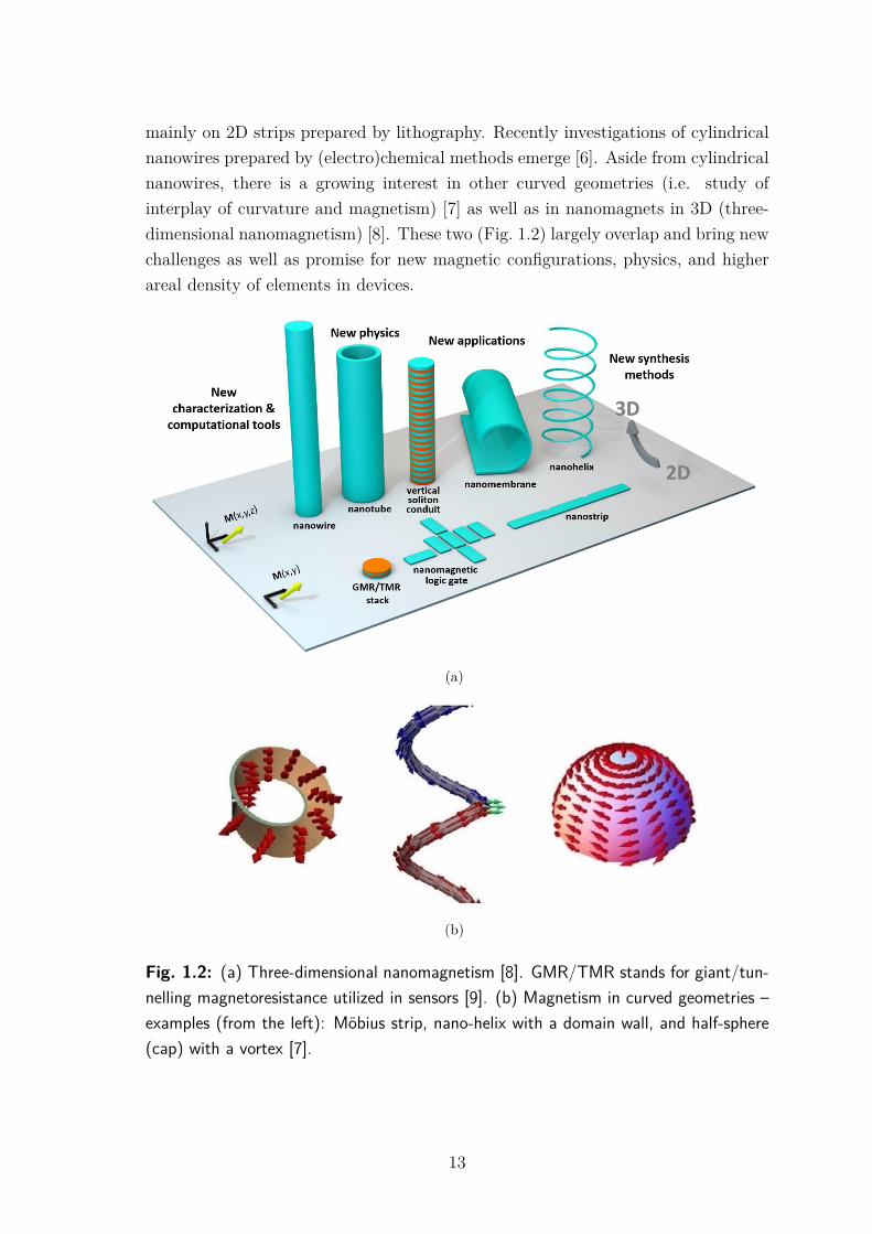
mainly on 2D strips prepared by lithography. Recently investigations of cylindricalnanowires prepared by (electro)chemical methods emerge [6]. Aside from cylindricalnanowires, there is a growing interest in other curved geometries (i.e. study ofinterplay of curvature and magnetism) [7] as well as in nanomagnets in 3D (three-dimensional nanomagnetism) [8]. These two (Fig. 1.2) largely overlap and bring newchallenges as well as promise for new magnetic configurations, physics, and higherareal density of elements in devices.
(a)
(b)
Fig. 1.2: (a) Three-dimensional nanomagnetism [8]. GMR/TMR stands for giant/tun-nelling magnetoresistance utilized in sensors [9]. (b) Magnetism in curved geometries –examples (from the left): Möbius strip, nano-helix with a domain wall, and half-sphere(cap) with a vortex [7].
13
Magnetic nanowires and nanotubes
In nanomagnetism and spintronics, magnetic domain wall motion has been mainlyinvestigated in flat strips prepared by lithography [5, 10]. However, magnetic nan-otubes (NTs) and cylindrical nanowires (NWs) fabricated in vertical arrays bybottom-up methods are more suitable for the design of high density storage deviceswith 3D architecture.
Ten years after the initial proposal for the 3D racetrack memory, the focus is shift-ing from experiments on arrays of cylindrical nanowires to single-nanowire physics,based on transport [11], magnetometry [12], and imaging [13] involving the first ex-perimental confirmations of DWs [14, 15]. These nanowires could provide a modelsituation for DW motion under magnetic field [16] or spin-polarized current [17]as fast (> 1 km/s) DW motion has been predicted in these wires [17]. However,DWs in magnetically-soft nanowires are of head-to-head or tail-to-tail type due tothe axial magnetization in the domains, which is inherently associated with a largemagnetostatic monopolar charge. The resulting long-range stray field could induceunwanted interactions (cross-talk) among densely-packed elements in a device. Thenewest solution, how to circumvent this issue, relies on artificial materials, so calledsynthetic antiferromagnets that generate no stray field. While the concept has beendemonstrated for 2D flat nanostructures [5], the 3D implementation has not beenrealized so far.
Magnetic nanotubes, less exploited in comparison to the simple nanowire geom-etry, have been reported mainly in the context of biomedicine [18] and catalysis [19],while their individual magnetic properties have been largely overlooked. Yet the-ory and simulations predict similar physics of domain walls in nanotubes comparedto cylindrical nanowires [20, 21], including fast (> 1 km/s) DW motion withoutWalker instabilities [22]. In terms of new physics and devices, nanotubes appearto be more suitable than solid nanowires. Indeed, their magnetic properties canbe tuned by changing the tube wall thickness, and more complex architectures canbe prepared based on core-shell structures [23]. These are analogous to multilayersin 2D spintronics (spin-electronics), such as magnetic layers separated by a thinnon-magnetic spacer for sensors based on magnetoresistance effects [9] or syntheticantiferromagnets mentioned above.
Further, as it has been already done in case of nanowires [24–26], one can tune themagnetic properties and functionality of potential devices by modifying propertiesalong the tubular structures (modifications could be used also for definition of bitsin the racetrack memory):
• material: composition, segments from different elements [27], doping, irradia-tion . . .
14

• geometrical change: diameter modulation [28], constriction, notches-defects,wire-tube elements [29, 30]
• core-shell structures [23] / multilayered tubes [31].
Why magnetic nanotubes?
In this work we are concerned only with magnetic properties and possible appli-cations of nanotubes in spintronics. Aside from these, they have other propertiesinteresting for different fields, e.g. large surface area – useful for catalysis. Further,both inner and outer surface can be functionalized and/or molecules (drugs) can beloaded inside the tube.
Magnetic nanotubes can bring new or enhanced phenomena due to their geome-try, different topology compared to flat films, and possibility to create more complexstructures and devices based on multilayered nanotubes (Fig. 1.3).
Curvature Closed surface Core-shell
Fig. 1.3: Specific features of nanotubes – 3C: Curvature (curvature induced ef-fects), Closed surface (different topology), and Core-shell geometry (multilayered tubes).
Namely curvature leads to breaking of an inversion symmetry: one can distin-guish the inner and the outer surface. This does not happen for a perfect flat film,but only for multilayers – magnetic layer sandwiched in between two different (non-magnetic) layers. Therefore, in this regard, a magnetic tube (curved surface) isequivalent to a multilayered flat film/strip. In flat systems like Pt/Co/AlO𝑥 films(with ultrathin Co and thus perpendicular magnetization), breaking of the inversionsymmetry is associated with promotion of chiral magnetic textures, fast propaga-tion of magnetic domains [32], and non-reciprocity of spin wave propagation [33].Similar phenomena indeed should arise in case of magnetic nanotubes (single mag-netic layer, no additional layers needed): curvature induces magnetochirality [34],anisotropy and a so-called effective Dzyaloshinskii-Moriya interaction [7]. Recently,theoretical predictions of the non-reciprocity of spin wave propagation in the tubeshave emerged as well [35, 36].
An open and exciting question is whether one can combine effects arising fromboth curvature and interfaces with different materials and make the effects (e.g.the effective Dzyaloshinskii-Moriya interaction) even stronger. Combination of such
15

core-shell structures with modification of properties along the structures as pointedabove (material, geometry) could lead to e.g. novel magnonic (spin-wave) waveg-uides. Some core-shell nanowires have been already realized, such as spin-valves [37].However, most of the possible stacks still awaits: synthetic antiferromagnets, struc-tures with heavy metals (such as Pt) exploiting the Spin Hall effect [38, 39] or theDzyaloshinskii-Moriya interaction (see section 2.2.1) [40] . . . Vertical arrays of suchmultilayered nanotubes could enable transfer of 2D spintronics to 3D and thus makespintronic devices more viable and competitive.
Chemists and material scientists can fabricate huge variety of nanostructuresfrom different materials and with various shapes. This involves magnetic nan-otubes, multi-layered tubes and core-shell nanowires. However, characterizationof such structures is done by global measurements, typically by magnetometry onarrays or bundles of such structures. On the other hand, physicists can image andmeasure single nanostructures, but so far they have been focusing mostly on thinfilm elements prepared by lithography. More recently some of them moved on tothe study of cylindrical nanowires prepared by chemical methods. In this work webring together these two worlds. The author himself is a hybrid of an engineer, aphysicist, and a chemist. We also build on a collaboration with expert chemists andmaterial scientists from TU Darmstadt, in particular with Sandra Schaefer.
Organization of the manuscript
The presented manuscript is divided into 4 parts:• I: Theoretical background & State of the art• II: Methods & Instrumentation• III: Results & Discussion – Magnetic nanotubes• IV: Results & Discussion – Multilayered nanotubesThus, we will start with a review of theoretical background and information on
what has been already done in the field of elongated magnetic nanostructures andnanotubes in particular. Part II describes techniques we used in our investigation aswell as some related supporting information. Finally results (both experiments andnumerical modelling) are discussed in parts III and IV, with part III being focusedon magnetic nanotubes and the last one on more advanced core-shell structures(multilayered tubes).
16

Part I
Theoretical background & State ofthe art
17
2 MAGNETISM IN LOW DIMENSIONS
In this chapter, upon briefly discussing different magnetic orderings, we will focus onferromagnets. We will treat them in the framework of a so-called micromagnetism.This continuum theory is especially suitable for the description of nanostructureswhich form usually too large systems to be addressed by (relativistic) quantum me-chanics, however, still too small to be described by the phenomenological Maxwell’stheory of electromagnetic fields. Micromagnetism bridges the gap between these twoapproaches - assuming continuum while taking some results derived from quantummechanics. For basics of magnetism or other methods how to treat it, one mayconsult the following (text)books [41–43].
2.1 Magnetically-ordered materials
Below we briefly cover materials that are magnetically ordered. Note that the samematerials may display different ordering and/or total magnetic moment dependingon conditions such as crystallographic structure (influenced also by following param-eters), temperature, stress, electric field etc. Magnetic ordering can be also differentif the size of the material is decreased to nanometric dimensions; material defectsplay a role as well. We can distinguish 3 main groups of magnetically ordered ma-terials: ferromagnets, ferrimagnets and antiferromagnets. Atoms in these have netmagnetic moments and these moments strongly interacts creating regions with mo-ments aligned (parallel) in one direction – so called domains (to be discussed below).In our work we will focus on materials exhibiting ferromagnetic behaviour.
Ferromagnets
The interaction of magnetic moments in ferromagnets leads to their preferentialalignment parallel to the same direction. Therefore, ferromagnets can have a strongnet magnetic moment. The volume density of the moment is referred to as mag-netization. Despite strong magnetic moments, the whole ferromagnet can have aweak net moment due to the presence of ordered regions (domains) with differentorientation of the common axis for the magnetic moments (e.g. demagnetized state).
Antiferromagnets
Magnetic moments in antiferromagnets have a common axis, but they are ordered inantiparallel directions leading to zero net magnetic moment. As such, antiferromag-nets are uneasy to be influenced by the external magnetic field. On the other hand,
18

even antiferromagnets can be manipulated with spin polarized current and antifer-romagnetic spintronics becomes a hot topic thanks to faster spin dynamics com-pared to ferromagnets [44, 45]. Typical time-scale for spin precession and reversalin antiferromagnet (dominated by strong exchange interaction) is in the picosecondrange (THz frequency), whereas magnetization dynamics in ferromagnet happensmostly at nanosecond scale (GHz frequency). Currently, antiferromagnets are usedin spin-valves to fix the magnetization in a ferromagnetic so-called reference layerthrough ferromagnetic/antiferromagnetic coupling (makes the ferromagnet magnet-ically harder).
Ferrimagnets
Ferrimagnets are usually composed of atoms forming 2 sub-latices from differentelements, or same elements, but having different oxidation number, occupying dif-ferent crystallographic site, . . . . Magnetic moments in one lattice are ordered inantiparallel direction with respect to the moments in the other lattice. The mate-rial still have some resulting magnetic moment as the magnitude of the moment ofatoms from the two different sub-latices is not the same except at one particulartemperature for some of them. At this point, so-called magnetic moment compen-sation temperature, temperature dependence of the magnetic moment magnitudeleads to zero net magnetic moment. Such compensation is observed in garnets andrare-earth–transition-metal alloys, but not in magnetite.
Aside from this, ferrimagnets may have another compensation temperature. It isangular momentum compensation point where the net angular momentum vanishes.Recently ferrimagnets regained attention thanks to findings indicating very interest-ing properties near such temperature: ultra-fast magnetization switching similar toantiferromagnets [46] and possibility to achieve magnetic field-controlled antiferro-magnetic spin dynamics [47]. Moreover, recent simulations show that domain-walldynamics in ferrimagnets subject to Dzyaloshinskii-Moriya interaction (DMI) canbe associated with emission of terahertz spin-waves [48]. One may thus think aboutspintronics based on ferrimagnets, as these unlike antiferromagnets can be moreeasily manipulated, especially by external magnetic field.
Synthetic antiferromagnets
Aside from above-mentioned materials present in nature, one can create artificial ma-terials – synthetic antiferromagnets (SAFs) and ferrimagnets based on heterostruc-tures composed of two (ferro)magnetic layers separated by a thin spacer. Exampleof such spacer is Ru, but other (transition) metals and even semiconductors/insu-lators can be used [49] (possibly different mechanism – spin polarized tunnelling).
19

Inter-layer magnetic Ruderman-Kittel-Kasuya-Yosida interaction (RKKY, indirectexchange), leads to parallel (ferromagnetic) or antiparallel ordering of magnetizationin the two layers depending on the spacer nature and its thickness (typically around1 nm). The interaction oscillates in between these two regimes and its strengthdecreases with the spacer thickness [50].
SAFs can be easier to prepare than genuine antiferromagnets and they havesimilar fast magnetization dynamics (also very fast domain wall motion) [51, 52]. Inaddition, SAFs offer more versatility in terms of tuning the magnetic moments andthe Néel temperature (above this temperature there is no more antiferromagneticorder). In practice, it is difficult to obtain the same magnetic moments of the twomagnetic layers, thus one obtains a synthetic ferrimagnet. Recent experiments onsuch structures in form of strips show promising results [53].
In this thesis we will restrict our exploration to ferromagnetic nanotubes andpartially we will also touch tubular multilayers. But as will be shown later, anti-ferromagnetic nanotubes can be prepared and in theory ferrimagnetic tubes maybe exploited as well. However, note that just ferromagnetic tubes alone are not sowell explored from the experimental point of view not speaking of other possiblemagnetic orderings.
2.2 Micromagnetism
Micromagnetism, sometimes merged with nanomagnetism (magnetism at nanoscale),is suitable for the description of magnetism at mesoscopic scale – i.e. micro andnanostructures. The micromagnetism is a continuum theory of magnetism, wheremagnetization is supposed to be a continuous function of a position in space. Inaddition, it is assumed that the magnetization vector has a constant norm for ho-mogeneous materials, thus only the direction of magnetization is allowed to change:
��s = ��s(��),��s
= const. (2.1)
The topic will be covered only briefly without derivations and provision of deeperinsight. Interested reader is encouraged to consult an excellent book Magnetic Do-mains [54] and other helpful resources [55, 56].
We used this approach in numerical modelling of magnetization in our nanos-tructures (tubes, wires).
20
2.2.1 Energies at play
There are various contributions to the total energy of a (micro)magnetic system,among them the most important ones are: exchange, magnetostatic (dipolar), Zee-man (energy in external magnetic field), magnetocrystalline anisotropy and mag-netoelastic energy. The interplay of these energies determines the magnetizationconfiguration of a sample and affects its evolution, dynamics.
Exchange energy
This contribution results from a purely quantum mechanical interaction betweenspins (more generally magnetic moments). In case of the direct Heisenberg exchange,the exchange energy of two spins ��1, ��2 reads [42]:
𝐸ex,spin = −𝐽1,2��1 · ��2, (2.2)
With constant 𝐽 representing the value of exchange integral; for ferromagnets 𝐽 > 0and alignment of neighbouring spins in the same direction is preferred. In the micro-magnetic continuum approach, if the magnetization in a ferromagnet deviates fromthe uniform one, an energy penalty in the form of an isotropic volume 1 exchangestiffness energy appears:
𝐸ex = 𝐴y
ferromagnet
⎛⎝∇ · ��
𝑀s
⎞⎠2
d𝑉, (2.3)
where 𝐴 is the exchange stiffness with dimension J/m. At zero temperature, stillused in many simulations, its value is loosely related to the critical Curie tem-perature 𝑇c: 𝐴(𝑇 = 0 K)≈ kB𝑇c/𝑎L, with kB being Boltzmann’s constant and 𝑎L
lattice parameter of the ferromagnetic crystal [54]. Typical value are of the order of10 pJ/m: around 30 pJ/m for cobalt and 10 pJ/m for permalloy (Ni80Fe20) [43].
For minimization of the exchange energy, uniform magnetization �� is preferred.Generalized expression states:
𝐸ex =y
ferromagnet
∑𝑖,𝑘,𝑙
𝐴𝑘𝑙𝜕
𝜕𝑥𝑘
(𝑀𝑖
𝑀s
)𝜕
𝜕𝑥𝑙
(𝑀𝑖
𝑀s
)d𝑉. (2.4)
Fortunately, symmetric tensor 𝐴𝑘𝑙 reduces to a simple scalar for cubic or isotropicmaterials, thus the isotropic stiffness expression (2.3) can be used [54].
1There exist also interface exchange coupling, when two different ferromagnets are in contact.This case is far beyond the scope of this work.
21

Asymmetric exchange (Dzyaloshinskii-Moriya interaction)
Above we discussed the common symmetric exchange interaction. However, asym-metric exchange, so-called Dzyaloshinskii-Moriya interaction [40, 57], exist as welland is extensively investigated in spintronics. Starting again from the atomisticdescription with 2 spins, the energy associated with this interaction reads:
𝐸DM,atom = 𝑑1,2 ·(��1 × ��2
), (2.5)
with 𝑑1,2 being the Dzyaloshinskii-Moriya interaction vector for the atomic bond.While the symmetric exchange (2.2) favours co-linear spin arrangements (paralleland anti-parallel spins), the DMI promotes spin-canting and textures such as spin-spirals, (anti)skyrmions. The DMI is present in bulk materials that do not have spaceinversion symmetry and more important it may also arise at the interface of ferro-magnetic thin films and materials with high spin-orbit coupling (e.g. Pt/Co/AlO𝑥
multilayer – both interfaces play a role). As mentioned in the introduction, the DMIis associated with the breaking of the inversion symmetry, leading to magnetochi-rality, non-reciprocity of spin-wave propagation etc.
For ultra-thin films the DMI energy can be written in the micromagnetic con-tinuum approximation as follows [58, 59]:
𝐸DM = 𝑡x
film
𝐷
[(𝑚𝑥
𝜕𝑚𝑧
𝜕𝑥− 𝑚𝑧
𝜕𝑚𝑥
𝜕𝑥
)+(
𝑚𝑦𝜕𝑚𝑧
𝜕𝑦− 𝑚𝑧
𝜕𝑚𝑦
𝜕𝑦
)]d𝑆, (2.6)
where 𝐷 is is the continuous effective DMI constant ([𝐷]=J/m2), 𝑡 is the filmthickness, 𝑚𝑖 = 𝑀𝑖
𝑀sthe normalized magnetization vector, and 𝑧 is axis perpendicular
to the film.In case of our samples, magnetic tubes, we do not consider the DMI. Proper
treatment of the DMI in magnetic tubes is beyond the scope of our work. Inter-ested readers may consult a theoretical work by Goussev dealing with DMI in thetubes [60], note that the work claims some important differences for DMI in planarfilms (wires) and tubes. As already stated, effects similar to the one induced byDMI can arise from the curved geometry itself.
Zeeman energy
The Zeeman term describes energy of a magnetic moment in an external magneticfield. This contribution gives an energy penalty if the magnetization does not lie inthe direction of the external applied field:
𝐸Z = −µ0
y
ferromagnet
�� · ��ext d𝑉. (2.7)
22

Magnetostatic energy
Magnetostatic (dipolar) energy describes Zeeman-like mutual interactions of mag-netic moments in a ferromagnet and reads:
𝐸d = −12µ0
y
𝑉
�� · ��d d𝑉, (2.8)
With integration taken over the ferromagnet volume 𝑉 which defines a closedsurface 𝜕𝑉 ≡ 𝑆.
Sometimes an energy density called dipolar constant 𝐾d = 12µ0𝑀
2s is used. While
demagnetizing field ��d has zero curl, it results from a potential: ��d = −∇𝜑d. Usingthis notation and the concept of magnetic charges, magnetostatic energy can beexpressed in a different form [54]:
𝐸d = µ0𝑀s
⎛⎝y
𝑉
𝜌m𝜑d d𝑉 +{
𝜕𝑉
𝜎m𝜑d d𝑆
⎞⎠ . (2.9)
In analogy with electrostatics 2, volume (𝜌m) and surface (𝜎m) density of mag-netic charges (shortly just charges) are defined as:
𝜌m = −µ0∇ · �� = µ0∇ · ��, (2.10)
𝜎m = µ0�� · ��. (2.11)
Second part of (2.10) originates in inserting 3 material relation �� = µ0�� +µ0�� intoMaxwell equation ∇ · �� = 0. Vector �� in (2.11) denotes outward-directed surfacenormal. Note that very often the volume magnetic charges are defined simply as𝜌m = ∇ · �� .
To minimize 𝐸d, we need to reduce both volume and surface charges, which leadsto a so called charge avoidance principle. Surface charges can be avoided when themagnetization lies parallel to the sample edges, which can lead to a so called fluxclosure as will be shown later. The shape of the sample – integration region – hasalso a significant influence on the magnetization configuration. Sometimes we speakabout shape anisotropy in this case and consider 𝐾d as a anisotropy constant (seeeffective anisotropy below). However, the shape anisotropy is not related to otheranisotropies like the magnetocrystalline one, which will be cover in the next section.
Magnetocrystalline anisotropy
In a crystal not all directions of the magnetization have the same energy. Due tocrystal-field effects, coupling electron orbitals with the lattice, and coupling of elec-tron orbitals with spins, some directions (or planes) with respect to the crystal axes
2∇ · �� = 𝜌e𝜖0
and therefore ∇ · �� = 𝜌m𝜇0
.3(
∇ · �� = 0)
∧(
�� = µ0�� + µ0��)
⇒ −µ0∇ · �� = µ0∇ · �� = 𝜌m.
23

are preferred. These are so called easy axes (or easy planes/surfaces). On the otherhand, less favoured hard axes exist [56]. Rigorous treatment of magnetocrystallineanisotropy is quite complex as well as formulas used for its description, interestedreader may consult references [41, 43, 54]. Very often volume density of magneticanisotropy energy is given in terms of a set of angular functions. Here we will re-strict ourselves to simple example of a uniaxial anisotropy found in hexagonal andorthorhombic crystals:
𝜖mc,u = 𝐾1 sin2 𝜃 + 𝐾2 sin4 𝜃 + · · · , (2.12)
where 𝐾𝑖 are anisotropy constants with dimension J/m3 and 𝜃 is angle betweenmagnetization and the anisotropy axis. Anisotropy constants for higher power termsare usually negligible and sometimes only the first term is taken into account. Cobaltis a typical represent with 𝐾1 = 520 kJ/m3 and the 𝑐 axis of the hexagonal crystalbeing the only easy axis [56].
Magnetoelastic coupling
So far we have spoken of an undeformed lattice. External stress results in strainand magnetoelastic contribution which is sometimes taken as a part of magnetocrys-talline anisotropy. Local deformation may result from stress generated by the fer-romagnetic material itself – magnetostriction [43]. Inverse magnetostriction (Villarieffect) describes change in magnetization (and other magnetic properties) when thematerial is strained (external influence, stress).
2.2.2 Characteristic lengths
As a consequence of a competition of different interactions, characteristic quantitiessuch as lengths arise. We will mention here only two of them [56]:
• anisotropy exchange length (Bloch parameter): Δa =√
𝐴𝐾a
,• dipolar exchange length (exchange length): Δd =
√𝐴
𝐾d.
Δa is important for hard magnetic materials, where exchange and anisotropy (withanisotropy constant 𝐾a) compete. This length corresponds to a width of a domainwall (discussed below) separating two domains. For soft magnets, Δd with exchangeand dipolar energy competition is more relevant. Δa is roughly 1 nm for hard mag-nets and up to several hundreds nanometers for soft magnets. Δd lies near 10 nm forboth types [56]. Therefore we see, that nanoscale is really important in magnetism.These exchange lengths have importance in micromagnetic simulations where smallvolumes of a magnetic body are supposed to be described by one magnetic moment.
24

2.2.3 Magnetization dynamics
Magnetization dynamics, i.e. the evolution of magnetization, is described by theLandau-Lifschitz-Gilbert (LLG) equation:
d��
d𝑡= 𝛾G�� × ��eff + 𝛼G
𝑀s�� × d��
d𝑡. (2.13)
The first term stands for Larmor precession of the magnetization around an ef-fective magnetic field ��eff (typically external magnetic field, but there could beother, internal, contributions such as magnetostatic, anisotropy, and exchange).𝛾G = −µ0𝑔
e2𝑚e
is the Gilbert gyromagnetic ratio, with e being the elementary chargeand 𝑚e the mass of the electron. The Landé 𝑔 factor has value close to two for manyferromagnets [54]. The gyromagnetic ratio links magnetic moment �� with angularmomentum ��: �� = 𝛾��. As we know from mechanics, d��
d𝑡= 𝑇 , where 𝑇 stands for
torque. Thus all the terms on the right-hand-side of (2.13) can viewed as torques 4
multiplied by a constant.In real magnetic systems there are losses that cause damping of the preces-
sional motion. In the end, magnetization is oriented parallel with respect to ��eff ,as expected 5. This is described by the second term in (2.13) with 𝛼G being the di-mensionless empirical (phenomenological) Gilbert damping parameter with typicalvalues for real materials 10−3−10−1. It describes further unspecified dissipative phe-nomena such as magnon scattering on lattice defects. Note that some damping-liketorques can have opposite sign and lead to an effective negative damping constant𝛼. Vectors and terms acting in the LLG equation are depicted in Figure 2.1.
The effective magnetic field is given by:
��eff = −1µ0
δ𝐸
�, (2.14)
where 𝐸 is the total energy of the system under consideration. Particular energycontributions have been already described above.
New phenomena in magnetization dynamics such as spin transfer [62] and spinorbit torques [63, 64] or the Dzyaloshinskii–Moriya interaction [40, 57] can be in-corporated into the LLG equation (2.13) as additional torques (on the right hand
4We recall that the torque acting on a magnetic dipole in an external magnetic field is given by𝑇e = �� × µ0��.
5Magnetization precessional dynamics can be viewed as analogue of a gyroscope in mechanics.Even though antiparallel alignment of �� with respect to ��eff in case of negative 𝛼G might be asurprise, it has its mechanical analogy as well: special spinning tops having a low lying centre ofgravity – tippe tops. Some readers may recall the photo in which even Wolfgang Pauli and NielsBohr were fascinated by upside-down flip of the tippe top [61, Fig. 3.18].
25

Fig. 2.1: Schematic picture of the dynamics of a magnetization vector (or magneticmoment) – graphical representation of the LLG equation. Torque 𝑇 = �� × ��eff actson the magnetization �� in an effective field ��eff . This leads to a precession of themagnetization around ��eff in a direction opposing 𝑇 , because 𝛾G is negative. In caseof non-zero damping 𝛼, a damping torque 𝑇d emerges. It is related to the second termin the LLG equation. For a common case of positive 𝛼 it aligns the magnetization withthe effective field. Therefore the end point of �� goes in a spiral before it reaches finalstate (angle 𝜃 = 0). Typical time-scale for this process is in the order of nanoseconds.Adapted from [61].
side of the LLG) [65], or included in the effective magnetic field ��eff as new energycontributions, respectively.
2.3 Magnetic domains and domain walls
2.3.1 Origin of magnetic domains and domain walls
Usually only tiny nanomagnets (or magnets subjected to a strong uniform exter-nal field) are uniformly magnetized, larger magnets are split into several magneticdomains, regions with (almost) uniform magnetization, however, with different mag-netization direction in the neighbouring regions (domains). The presence of domainsresults from competition of particular energy contributions, mainly exchange, mag-netostatic, and anisotropy energy. It also depends on the magnetic history of thesample: during a hysteresis cycle, sample may display different amount, sizes andeven types of domains. Usually larger number of domains can be obtained upondemagnetization of a sufficiently large sample. How the competition of differentenergies influences magnetization in a spheroidal particle is illustrated in Figure 2.2.Exchange energy alone favours uniform magnetization, thus only one domain ispresent – we speak of a single domain-state. If we consider also the magnetostaticinteraction, a flux-closure pattern appears as a tendency to minimize surface charges
26

by keeping magnetization parallel to the particle edges. Anisotropy may favour onlycertain directions of the magnetization, e.g. in case of uniaxial anisotropy, two do-mains could be more favourable than the complete magnetic flux-closure. In suchcase, domains are separated by a boundary, a domain wall (DW). Domain theoryis very complex and there is no single and simple origin of domain creation for allmaterials. It rather differs from case to case, depending on anisotropies, shape andsize of sample, and magnetic history of the sample. Magnetostatic energy plays animportant role in this case [54]. For rigorous treatment and nice pictures of variousdomains (bamboo, bubble, spike, labyrinth, saw-tooth, . . . ) consult the excellentbook Magnetic domains [54].
Fig. 2.2: Influence of energy contributions on a spheroidal particle. In first particle(from the left), only exchange is taken into account, thus uniform magnetization ispresent. In the middle flux-closure pattern results from competition of exchange andmagnetostatic energy. On the right, particle with a considerable uniaxial anisotropy issplit into two domains as intermediate directions of the magnetization are unfavourable.Gray line represents the the domain boundary – domain wall. Adapted from [43].
Here, we will focus on so-called 1D nanostructures – nanostrips, cylindricalnanowires, and mainly nanotubes – the main topic of the thesis. Even-thoughthese are (especially in experiments) 3D objects, in some cases the magnetizationand its dynamics can be approximated by a simple 1D model. We mention stripsand nanowires as these have been already thoroughly investigated and some simi-larities can be found in case of nanotubes. Regarding nanotubes, most of the worksare theory and simulations and only recently only few single tube experiments haveemerged.
2.3.2 Domain walls in nanostrips
In nanostrips, usually prepared by lithography from thin films, magnetization tendsto be in-plane. In this case two types of DWs can be observed: transverse and vortex(Fig. 2.3a,b). In nanostrips with magnetization perpendicular to the plane (e.g. verythin films) Néel and Bloch walls can be found (Fig. 2.3c,d). The DW type, Blochvs Néel, depends mainly on the film thickness. The transition is reported around20-40 nm for 180∘ DWs and magnetically-soft films. However, it can be affected byan additional magnetic anisotropy, such as magnetocrystalline [66].
27

(a) Transverse wall (b) Vortex wall
(c) Néel wall (d) Bloch wall
Fig. 2.3: Scheme of domain walls in nanostrips. (a)-(b) Strips with in-plane mag-netization with domain walls of (a) transverse and (b) vortex type. (c)-(d) Strips without-of-plane magnetization with (c) Néel and (d) Bloch wall. Arrows depict local mag-netization; domain wall region is highlighted with the blue colour. Schemes courtesy ofOlivier Fruchart.
2.3.3 Domain walls in cylindrical nanowires
In cylindrical nanowires with axial domains, two DW types were predicted [16,67, 68] and more recently also experimentally observed: transverse wall (TW) [14]and Bloch point wall (BPW) [15]. The first one has some similarities with bothtransverse and vortex walls in nanostrips. However, the other one has differenttopology and dynamics due to the magnetization curling around a Bloch point, amagnetic singularity where magnetization vanishes. TW wall is energetically moreviable in nanowires with a smaller diameter, BPW in larger ones. The transitionhappens around seven times the (dipolar) exchange length, roughly 35 nm in case ofpermalloy. Note that TW, with magnetization curling on both sides, can be presentin significantly thicker wires [14]. The wall type observed in experiments may alsodepend on the magnetic history of the sample.
2.3.4 Domain wall motion
Domain wall motion has been first (experimentally) investigated in thin films, flatnanostrips and more recently in nanowires. Only theoretical works exist in caseof NTs (more in section 3.2). Various stimuli can be applied to displace a DW.Aside from magnetic field and (spin-polarized) current, one can use the following:spin-waves [69, 70], thermal gradients [71], non-uniform stress (in magnetostrictivematerials) [72], and acoustic waves (creating stress) [73].
The motion, its dynamics and speed of DW propagation depend on the material,
28
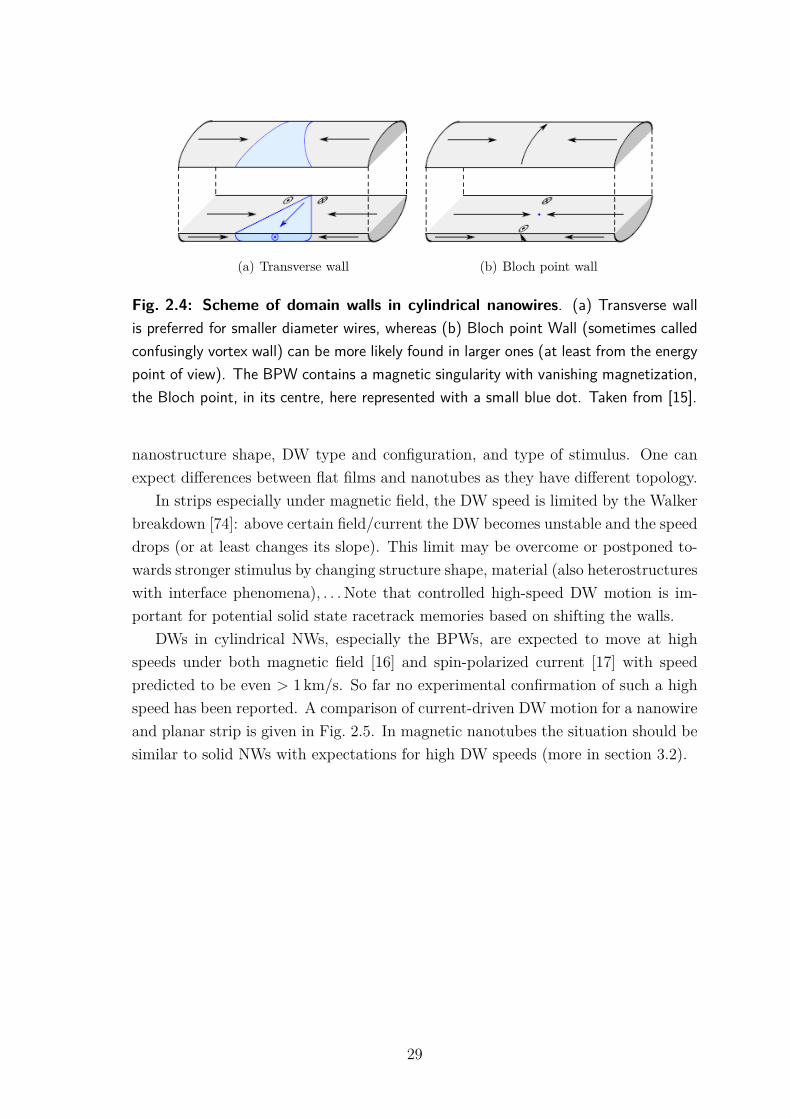
(a) Transverse wall (b) Bloch point wall
Fig. 2.4: Scheme of domain walls in cylindrical nanowires. (a) Transverse wallis preferred for smaller diameter wires, whereas (b) Bloch point Wall (sometimes calledconfusingly vortex wall) can be more likely found in larger ones (at least from the energypoint of view). The BPW contains a magnetic singularity with vanishing magnetization,the Bloch point, in its centre, here represented with a small blue dot. Taken from [15].
nanostructure shape, DW type and configuration, and type of stimulus. One canexpect differences between flat films and nanotubes as they have different topology.
In strips especially under magnetic field, the DW speed is limited by the Walkerbreakdown [74]: above certain field/current the DW becomes unstable and the speeddrops (or at least changes its slope). This limit may be overcome or postponed to-wards stronger stimulus by changing structure shape, material (also heterostructureswith interface phenomena), . . . Note that controlled high-speed DW motion is im-portant for potential solid state racetrack memories based on shifting the walls.
DWs in cylindrical NWs, especially the BPWs, are expected to move at highspeeds under both magnetic field [16] and spin-polarized current [17] with speedpredicted to be even > 1 km/s. So far no experimental confirmation of such a highspeed has been reported. A comparison of current-driven DW motion for a nanowireand planar strip is given in Fig. 2.5. In magnetic nanotubes the situation should besimilar to solid NWs with expectations for high DW speeds (more in section 3.2).
29

Fig. 2.5: Simulation – current-driven transverse wall motion in cylindrical wireand nanostrip (inset a1). 𝛽 is a so-called non-adiabatic spin-transfer parameter. Innanostrip so called Walker breakdown (arrows in the inset a1) with decrease in speedappears. Taken from [17].
30

3 MAGNETIC NANOTUBES
Here we will restrict ourselves to ferromagnetic metallic tubes of Ni, Fe, Co, andtheir alloys/compounds and possibly their combination with other materials. Wewill not cover carbon nanotubes, for these an interested reader may consult a recentbook Magnetism in Carbon Nanostructures [75].
In this chapter we discuss magnetic textures, mainly domains and domain walls,predicted in these tubes as well as some experiments reported on NTs. Further, weintroduce some common methods for fabrication of such NTs or even multilayered(core-shell) structures. Last but not least, we provide an overview of what has beendone on nanostructures with alternating wire (solid) and tube (hollow) segments.
3.1 Magnetic textures
One can think of various magnetic configurations in a nanotube. Some of these areschematically depicted in Fig. 3.1. Not all of them can be stable and other morecomplex states might be considered in case a special anisotropy is present.
Axial Azimuthal Onion Transverse Radial
Fig. 3.1: Possible magnetization configurations in a tube. Only a tube cross-section is shown. Depending on the geometry, axial (longitudinal) and azimuthal (curl-ing) states may span through the whole tube at remanence. In majority of elongatedtubes, the so-called mixed state is present – axial magnetization with small curling atboth tube ends. Under moderate external magnetic field applied in a transverse directionan onion state can develop. Upon further increase in the field magnitude it transformsinto a transverse state. The last, radial state, is rather unfavourable due to high exchangeenergy (large spatial variation of the spins), still it could exist in small tube regions as ametastable domain wall (to be further discussed later).
3.1.1 Magnetization phase diagram
Escrig [76], Landeros [77], and Sun [21] and coworkers presented phase diagramsfor magnetically soft NTs (considering exchange and magnetostatic energy) as a
31

function of tube diameter, tube wall thickness and length. In Fig. 3.2 one can seethe diagram by Landeros.
VF
Mixed
R - tube radius
L - tube length
lx - exchange length
β = Rinner/Router; β = 0: solid wire; β → 1: thin-walled tube
Fig. 3.2: Magnetization phase diagram of a soft magnetic tube. In nanotubeswith very small diameter the magnetization is axial everywhere (here denoted as F - fer-romagnetic state). For a tube with larger diameter, magnetization is still predominantlyaxial, but small curling develops at the tube ends (mixed state). Commonly F and mixedstates are labelled as axially magnetized. Short tubes with larger diameter prefer to be influx-closure state with azimuthal magnetization curling (V - vortex-like state). Favouredstates depend also on the tube wall thickness with global curling being found rather inthicker tubes. Graph and notation taken from [77].
Depending on the geometry, one of the two following states is preferred: ei-ther axial magnetization (possibly with localized curling close to the tube ends– so-called mixed state), or curling along the entire tube (azimuthal/circular/flux-closure/vortex-like magnetization). The uniform azimuthal state is the ground stateonly for short tubes with a large diameter (small aspect ratio) and large tube wallthickness, all to be compared with the dipolar exchange length. Note that themodels in [21, 76] overestimate the magnetostatic energy for the longitudinal mag-netization state by disregarding the possibility of a creation of the end curling fea-tures [21, 77, 78] i.e. formation of the mixed state. In other words, in these works,tubes with axial magnetization occupy a smaller part of the phase diagram com-pared to Landeros’ work [77]. Recently, the trends of geometrical dependence ofthe preferred state (axial, or azimuthal) were confirmed experimentally by Wyss etal. [79].
Other states such as transverse magnetization or onion state have been consid-ered in theory, but these can be stabilized only under external transverse magneticfield [21]. A uniformly magnetized domain (axial or azimuthal) is more favourable
32
than multidomain state with DWs [21]; these may exist as a metastable state or ineither large structures, or when additional anisotropy is present (e.g. magnetocrys-talline).
There has been quite some debate regarding the axially magnetized tubes andalso NWs with the end curling: is there a preference for the curling sense at the end?I.e. is the same or the opposite curling sense favoured at both tube ends? Recently ithas been shown, that this supposed preference was an artefact caused by too largemesh cell size in the numerical computation [79]. Refined simulations with 1 nmcell size showed that magnetic energy of the two states is equal (within numericalprecision), unless one considers tubes with aspect ratios approaching unity.
3.1.2 Azimuthal domains
So far most theoretical and experimental works have been concerned with tubeshaving axial magnetization. As stated above, such alignment of magnetization isexpected for elongated NTs, unless they exhibit some anisotropy (e.g. magnetocrys-talline, magnetoelastic).
Li and coworkers [80] prepared single-crystalline Co NTs by electroplating, graph-ical summary of their work is featured in Fig. 3.3. From global magnetometry onarrays of tubes, selective area electron diffraction and magnetic force microscopy(MFM) on single tubes they concluded that their tubes were in a flux-closure state(azimuthal magnetization) due to a magnetocrystalline easy axis being perpendic-ular to the tube axis. Magnetometry and diffraction indeed supported this finding;however, in our view the interpretation of the MFM results is questionable. In theirelectron microscopy images of tubes after template dissolution in sodium hydroxide,the tubes looked quite oxidized (hairy features on the surface, see the original imagein [80]). Li et al. mentioned that from previous experiments they estimated thecobalt oxide layer thickness to be 3 nm, however, they refer to work on nanowires,not nanotubes. In case of NTs, especially thin-walled as in their case (10-15 nm),tubes are likely to be almost completely oxidized as both inner and outer tube surfaceis exposed to the hydroxide. We experienced the same problem in our experiments.Therefore, it is more probable that their weak signal measured in MFM comes froman electrostatic contribution (also long-range as magnetic interactions), especiallyas this contrast does not change after annealing and no contrast is expected forflux-closure.
Further, the flux-closure domains were reported by Wyss et al. [79] in shorttubes using synchrotron magnetic microscopy (example in Fig. 3.4. In this thesis,we present similar observation, but with multiple domains and walls in significantlylonger tubes – consult chapter 8. For information on the imaging technique see
33

Fig. 3.3: Investigation of Co nanotubes with azimuthal domains by Li et al. [80].From the left: magnetometry on an array of the tubes with magnetic easy axis beingperpendicular to the tube axis, atomic and "magnetic" force microscopy investigation,and electron microscopy image of tubes after the template dissolution.
methods section 5.1.1.
Fig. 3.4: X-ray magnetic circular dichroism - photoemission electron mi-croscopy of permalloy tubes with azimuthal magnetization by Wyss et al. [79].Magnetic images of of a permalloy tube (diameter around 250 nm, shell thickness 30 nm)for beam perpendicular and parallel to the tube axis for (a) 1.3-µm-long and (b) 0.7-µm-long tube. Technique maps projection of magnetization to the beam direction. Thereforein (a) a single domain is present, whereas (b) features two domains. (c)-(d) Probablemagnetic states obtained from micromagnetic simulations (shorter tubes modelled).
3.2 Domain walls in magnetic nanotubes
Aside from coherent rotation of magnetization, the magnetization reversal in elon-gated NTs can proceed by nucleation and propagation of a DW [81]. In general,
34
all DWs in (magnetically soft) tubes are considered metastable [21], i.e. uniformaxial/azimuthal domain has lower energy. So far mainly walls in tubes with axialmagnetization have been considered (theory and simulations only, no experiments),still there are also several works dealing with walls between azimuthal domains. Thelatter is supposed to be found in tubes with small aspect ratios (mostly short tubeswith large diameters, thus not very appealing for most of applications). Below webriefly mention walls predicted in magnetic NTs. Only few experiments ([79], andour work) show azimuthal domains in nanotubes and/or even DWs. So far no DWcould be stabilized (or better to say trapped) and imaged in axially magnetizednanotubes.
3.2.1 Domain walls in nanotubes with axial domains
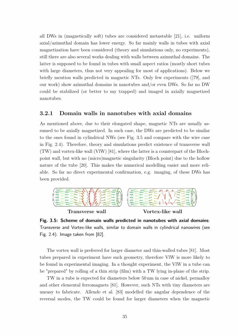
As mentioned above, due to their elongated shape, magnetic NTs are usually as-sumed to be axially magnetized. In such case, the DWs are predicted to be similarto the ones found in cylindrical NWs (see Fig. 3.5 and compare with the wire casein Fig. 2.4). Therefore, theory and simulations predict existence of transverse wall(TW) and vortex-like wall (VlW) [81], where the latter is a counterpart of the Bloch-point wall, but with no (micro)magnetic singularity (Bloch point) due to the hollownature of the tube [20]. This makes the numerical modelling easier and more reli-able. So far no direct experimental confirmation, e.g. imaging, of these DWs hasbeen provided.
Transverse wall Vortex-like wall
Fig. 3.5: Scheme of domain walls predicted in nanotubes with axial domains:Transverse and Vortex-like walls, similar to domain walls in cylindrical nanowires (seeFig. 2.4). Image taken from [82].
The vortex wall is preferred for larger diameter and thin-walled tubes [81]. Mosttubes prepared in experiment have such geometry, therefore VlW is more likely tobe found in experimental imaging. In a thought experiment, the VlW in a tube canbe "prepared" by rolling of a thin strip (film) with a TW lying in-plane of the strip.
TW in a tube is expected for diameters below 50 nm in case of nickel, permalloyand other elemental ferromagnets [81]. However, such NTs with tiny diameters areuneasy to fabricate. Allende et al. [83] modelled the angular dependence of thereversal modes, the TW could be found for larger diameters when the magnetic
35
field was applied close to a direction transverse to the tube axis. The predictedangular dependence of coercivity was experimentally confirmed by magnetometryon arrays of tubes [82, 84]. Later, Allende also modelled the propagation of TW intiny diameter-modulated NTs [85].
As the VlW should be the most common one in tubes, both theory and numericalsimulations focus on it. High speeds (> 1 km/s) have been predicted for such DWssubjected to axial magnetic field of just several mT (mobility 500 km s−1 T−1 forpermalloy) [22]; similar to its BPW counterpart in cylindrical NWs [16]. Also itappears that, unlike in flat strips, the maximum speed is not limited by the Walkerbreakdown [74]. There is another so-called magnonic limit, i.e. interaction with spinwaves created by the moving wall itself [22]. Under magnetic field, the DW dynamicsdepends on the chirality of the wall (respectively sense of circulation/curling ofmagnetization, type head-to-head or tail-to-tail) with respect to the applied fielddirection. Owing to the effect arising from the curved geometry [34], one chirality ispreferred and higher speeds are achieved for a wall (VlW) with such a chirality. If weincrease the field above certain threshold, the bad (unfavourable) chirality switchesto the preferred one and high speed motion is recovered [86, 87], see Fig. 3.6. Thisis similar to what happens in cylindrical wires for Bloch point wall under magneticfield [16]. Similar chirality dependence was obtained in simulation for VlW motion inpermalloy tube under azimuthal AC (almost 13 GHz) magnetic field with amplitudeof 5 mT: speed above 300 m/s was found for the field having the same curling sense asthe wall [88]. Note that such azimuthal field can be generated by a current-carryingwire inside the tube (i.e. producing Oersted field with the desired symmetry). Thiscan be achieved in core-shell nanowires/multilayered tubes. Such structures couldbe fabricated starting from magnetic tubes in a template, e.g. via depositing thininsulating oxide (HfO2) by atomic layer deposition and finally metallic core (Cu) byelectroplating. Similar structures have been already prepared – see section 3.5.
The DW motion was also investigated under the current [89] (up to 1013 A/m2
with DW speed of 1.2 km/s). Simulations yield speeds above > 1 km/s (with DWmobilities comparable to the case of DWs in strips with out-of-plane magnetizationand DMI), which should even increase with the tube diameter, and show a possibilityto switch on purpose the wall chirality by current pulses [86]. Further, spin-wave-induced DW motion was predicted to reach speeds up to 660 m/s [90].
Most of the above-mentioned simulations were performed only for permalloytubes without any anisotropy or special energy terms. Nevertheless, the latter wasinvestigated as well: namely effect of magnetocrystalline anisotropy on the wall type,width, speed, and the dynamics as a whole [91]. In addition to the tube curvaturegiving rise to DMI-like effects [7], VlW motion with DMI was considered. DMIin tubes (with axial [sic!] magnetization in domains) seemed to promote narrower
36

Fig. 3.6: Vortex-like wall speed under magnetic field for opposite chiralities [86].Analytical modelling for permalloy nanotube. One wall chirality is preferred and the wallmoves faster. The unfavourable chirality switches at a so-called chirality field 𝐻c andthe fast motion is recovered.
walls that propagate under current irrespective of the wall chirality. Under field, thespeed was chirality dependent as in case without DMI [60].
3.2.2 Domain walls in nanotubes with azimuthal domains
Magnetic domains and associated domain walls in systems with azimuthal magne-tization have been described (predicted) mostly in short tubes with large diameter,where azimuthal domains can exist even without special magnetic anisotropy. Leeet al. [92] modelled by micromagnetics a short permalloy tube (500 nm diameter,1000 nm length and tube wall thickness 100 nm). As a relaxed state, they obtained2 azimuthal domains separated by a DW that appears to have axial magnetization.Further, they introduced such tubes as a biaxial magnetic sensor and predictedanisotropic magnetoresistance of about 5 %. Experimental observation of such wallis claimed by Wyss et al. [79] and it is referred to as Néel wall due to a similarityof an unrolled tube with thin films. In case of these short tubes, one can discusswhether it is a Néel wall between azimuthal domains, or just axially magnetizedtube with end curling with the opposite sense of circulation . . .
Betancourt et al. [93] also simulated magnetization in short (500 nm), large diam-eter (500 nm) permalloy tubes (tube wall thickness 50 nm). As the relaxed state theyobtained two azimuthal domains separated by a cross-tie wall, i.e. counterpart of amagnetic structure with vortices and anti-vortices found in thin films/strips ([54],3.6.4 Domain Walls in Thin Films). Further, they also probed motion of this nar-row wall (supposedly 30 nm in width) in AC magnetic field (no DC component)applied in the azimuthal direction (Oersted field of a current-carrying wire insidethe tube). The wall speed increased with the field magnitude and was around 70 m/sfor 5.5 mT. Probably higher speeds can be obtained for larger fields. The maximum
37
speed occurred for frequency around 1 GHz with some slower motion observed up to10 GHz. Similar wall appeared in a work on rolled-up nanomembranes by Streubelet al. [94]. Micromagnetic simulation of a Ni tube with diameter 300 nm includingthe magnetostriction resulted in azimuthal domains. Even though the DWs werenot discussed in this case, they resembled the cross-tie ones.
In their theoretical paper [21], Sun and Pokrovsky briefly discussed the presenceof two possible walls between azimuthal (vortex-like) domains, without giving anynames or further description (schemes): "the magnetization rotates either in theplane (𝜑, 𝑧), or in the plane (𝜑, 𝜌)" with 𝜑, 𝜌, and 𝑧 being unit vectors in azimuthal,radial, and axial direction, respectively. We identify these as the Néel (axial) andthe Bloch (radial) walls, again in analogy with thin films. In section 9 we elaboratefurther on the walls types and provide images and micromagnetic simulations for all3 walls (Néel, Bloch, and cross-tie). We provide both simulations and experimentalimages of tubes with DWs in the same section.
Based on 2D micromagnetic simulations, for low aspect ratio (< 15) tubes withuniaxial anisotropy (along tube) and large tube wall thickness, another more exoticconfigurations (Branch, Horse-saddle, . . . ) were reported [95]. However, these are ofno interest in our work. It is also questionable whether all of them can be reproducedby full 3D simulations or even experiments.
3.3 Experiments on magnetic nanotubes
We have already mentioned some experiments performed on magnetic NTs and oth-ers will be discussed also in following sections. Nevertheless, here we provide a briefoverview of experiments from the literature that we are aware of. We will describeexperiments on tube arrays with nanostructures still in a template/matrix (e.g. na-noporous alumina) and measurements made on single (isolated) NTs. Note that fromthe experimental point of view it is much easier to study arrays of nanostructures,whereas in simulations usually only one or a few structures are modelled.
3.3.1 Experiments on nanotube arrays
The majority of experiments on NTs has been performed on NT-arrays. Such ex-periments are easier than inspection of individual tubes for several reasons. First,as tubes are commonly prepared in templates/matrices, one can use these directlywithout a need for further processing of the sample. The matrix makes the tubesmore mechanically stable and partially protects them from the oxidation – but notthe inner shell, unless additional protective layer is deposited or tube extremitiesare sealed. Such treatment is usually not applied, except for several works dealing
38

with tube fabrication via atomic layer deposition [28, 96] – here it is rather easy todeposit additional thin protective layer of silica or other oxides. Further, arrays, atleast for magnetometry, provide higher magnetic moment and thus signal. The maindisadvantage is that the measured quantity usually reflects average of many nanos-tructures with varying magnetic properties and geometry. Further, the behaviour ofthe tubes is influenced by magnetic dipolar interactions among them. Strength ofsuch interactions can be estimated e.g. from so-called first order reversal curves [97]or modelled (numerically often only for several tubes, but in principle parts of thearray can be effectively simulated using GPU-accelerated micromagnetic codes, suchas mumax3 [98]). Although some methods can access one tube in the template (e.g.magnetic force microscopy), one can detect only what happens close to the tubeend, and there is still the influence of the neighbouring tubes.
The most common experiment on NT-arrays is magnetometry [96, 97, 99] usinge.g. vibrating sample magnetometer (sometimes exploiting superconducting quan-tum interference device).
Bachmann et al. probed the geometry dependence of coercivity of magnetic tubearrays with the global magnetometry and found agreement with the theoretical pre-diction for magnetization reversal through nucleation and propagation of both trans-verse and vortex-like DWs [82]. Pathak and coworkers [100] performed magneto-optical measurement exploiting Kerr effect on arrays of Y-junction NWs with sometube segments, they could compare magnetization reversal at tube and wire ends.Tabasum carried out magnetic force microscopy, study of magnetization switchingin a tube array and its comparison with arrays of NWs [101]. T. Wang [102], Li [103]and Kozlovskyi [104] studied Fe3O4, FeCo, and FeNi NT arrays, respectively, withMössbauer spectroscopy, showing among others that magnetization lies predomi-nantly along the tube axis (expected for elongated tubes). Z. K. Wang et al. [105]conducted Brillouin light scattering spectroscopy on an array of Ni nanorings (aspectratio 1.5) and found spin wave frequency dependence on the axial magnetic field.Similar trend as in thin films was observed except for small fields (< 50 mT) wheremicromagnetic simulations predicted slightly different behaviour, but unfortunatelymeasurement points were not available in this region to confirm such behaviour.
Even though we focus of this section on experiments, we will briefly mentionrelated theoretical investigation of spin waves related to the experiments above.Magnons in NTs were described theoretically by Nguyen [106] confirming the trendschemed by Q. Wang (above). Gonzalez [107] worked further on the spin-wave dis-persion relation. And more recently Hertel [34] and Otalora et al. elaborated moreon possible modes and asymmetry in the spin wave dispersion relation and non-reciprocity of spin wave propagation in NTs [35, 36]. Most of these theoreticalpredictions still remain to be probed experimentally.
39

3.3.2 Experiments on single nanotubes
Experimental investigation of isolated NTs is much more challenging. This is also thereason why such experiments are still rather scarce. As porous templates are usuallyemployed for the synthesis, one has to dissolve the template, purify a solution withNTs and transfer the tubes on a suitable substrate and obtain clean and isolated NTs(not clusters). In other instances (e.g. when fabricating tubes using nanopillars [79]or putting tubes on a microcantilever [108]) one even has to micro-manipulate thetubes onto a suitable place. Further, some substrate patterning or even lithographyfor electrical contacting could be necessary. Last but not least, individual NTsprovide small magnetic signal (compared to solid NWs) and are also more prone tooxidation (both outer and inner surfaces exposed). Therefore, additional care shouldbe taken to protect the tubes from oxidation. Further, tube with large diametersand very thin shell thickness may require fortification to avoid deformation (suchelliptical cross-section instead of circular one). Both can be achieved at the sametime by atomic layer deposition of a thin non-magnetic layer.
Regarding the reported experiments we will start with work of Li et al. [80] whostudied individual single-crystalline Co NTs by magnetic force microscopy. Theyobtained weak uniform contrast which they interpreted as a sign of flux-closuredomain (magnetization curling/winding along tube perimeter). However, given thatthe tubes were exposed to NaOH during the template dissolution, and as the NTshad thin walls (10-15 nm), it is more likely that the tubes were oxidized and weakcontrast was of a non-magnetic origin (e.g. electrostatic interaction).
More convincing is an electron holography imaging of magnetic induction inshort magnetic tubes of hexagonal cross-section performed in the group of Dunin-Borkowski [109]. They found axially magnetized tube with magnetization curlingat the ends.
To the best of our knowledge, most experiments on single NTs have been donein the groups of Martino Poggio and Dirk Grundler (collaborating also with Dunin-Borkowski above, therefore similar samples with hexagonal cross-section were in-vestigated). Namely they performed magnetoresistance measurements of Ni [110],Py and CoFeB [111] NTs; cantilever torque and SQUID magnetometry [108], andrecently also magnetic imaging of CoFeB and permalloy NTs by synchrotron X-raymagnetic microscopy [79]. They imaged axially-magnetized tubes with end curlingstates (i.e. so-called mixed state, see e.g. Fig. 3.2) and azimuthal domain(s) in shorttubes with a sign of the Néel wall in some of them.
Note also, that so far no DWs in axially magnetized tubes have been experimen-tally observed, not speaking of studying their displacement or even dynamics (undermagnetic field or current).
40

In this thesis, we enrich these single tube investigations with similar synchrotronimaging (with higher resolution), but this time showing multiple well-defined do-mains and domain walls; magnetooptical measurements (with focused laser beam)and magnetic force microscopy with clear magnetic signal; all in chapter 8. Further,our electron holography investigation of higher aspect ratio CoNiB and NiFeB tubescan be found in sections 8.3.5 and 8.3.3.
3.4 Fabrication of magnetic nanotubes
The nanotube fabrication relies mostly on bottom up, (electro)chemical, methodsand use of templates (filling nanoholes or coating nanopilars). Chemical-based syn-thesis is utilized either for the whole deposition process, or at least for the templatesynthesis. Such template, e.g. if in the form of vertical pillars, can be coated byphysical (vapour) deposition [111]. There exist also template-free chemical synthe-ses [112], but template-assisted process is preferred as it provides better controlon geometry of the nanostructures. Further, it is possible to employ lithography,top-down approach, to prepare tubular structures. However, such way is so farinefficient, time consuming, and very limited in terms of geometrical parameters.
Various structures can be used as a template. The first division might be intoporous membranes (with holes; deposition inside) and (arrays of) pillars/wires (de-position on the outside surface). Note that for example biological microtubuli [113]or other tubes (e.g. carbon NTs) can serve as both (deposition inside/outside).There are other suitable bio-templates such as viruses (Tobacco mosaic virus [114]),but in most cases membranes with arrays of pores are preferred (easier processingand manipulation of larger amount of structures). These include porous alumina,mica, and track-etched polymeric templates – PolyCarbonate (PC), PolyEthyleneTerephthalate (PET) or even Kapton (chemically resistant – difficult to dissolve).In this work we use both most common types of porous templates – (nano)porouspolycarbonate [115] and alumina [116]; both are further discussed in methods sec-tion 4.1. The preparation of polycarbonate templates is also discussed in methodssection 4.4.1.
Below we provide more information on nanotube and core-shell nanostructurepreparation. Other information on the fabrication can be found in references [117–119].
3.4.1 Lithography
Top-down approaches, e.g. based on electron-beam lithography together with sput-tering or evaporation of a magnetic material, provide only tubes with small aspect
41
ratios (short tubes with large diameters). One should rather speak about rings asthe length (given by thickness of a film being patterned by the lithography) is ofthe same order as the diameter. In addition, both diameter and tube wall thicknessis limited to larger values (resolution limit of the lithography), therefore so far theprocess could not be down-scaled. Moreover, the deposition can be rather long andexpensive and cannot deliver such a high amount of NTs as bottom-up techniques.To give an example: Huang et al. [120] prepared short permalloy tubes with diame-ter of 300 nm, tube wall thickness 20 nm, and height 160-600 nm using electron-beamlithography together with ion-beam milling.
3.4.2 Electrodeposition
Electroplating in porous templates can yield tubes with diameters as small as25 nm [121] based on porous working electrode [122, 123], modified template porewalls [124] or other particular conditions (pH, current density, over-potential). Thematerial is of high quality, even single crystals can be obtained [80], but wire-vs-tube growth instabilities occur [125]. In addition, in some depositions, the tubesbecome thicker during the growth and they eventually transform into solid wiresas their length increases. One can prepare conductive deposits: pure metals andalloys. Semiconductors can be prepared as well, insulators (oxides) only after post-processing.
The problem with obtaining both NWs and NTs upon electrodeposition in cylin-drical nanopores can be overcome to some extent by using a template with tubularnanoholes - these can be prepared e.g. by deposition and controlled shrinking ofpolymeric NWs inside porous alumina [126]. Such approach offers better controlover the tube wall thickness, but it cannot be applied to very high aspect ratiostructures as the inner polymeric wire would collapse and block the pore.
More information with references are in the methods section 4.2, results of ourelectroplating are discussed in sections 7.1 and 7.2.
3.4.3 Electroless deposition
Electroless plating of magnetic (nano)tubes [127–129] provides good control overthe tube thickness [130], diameters down to 100 nm using porous templates [19] and50 nm in case of biotemplates [113]. Various materials can be deposited, oxides,magnetic and non-magnetic metals. Similar to atomic layer deposition (below) thegrowth can be conformal and even high aspect ratio pores can be filled. The tech-nique is also suitable for deposition of multilayers [31], which we demonstrate in
42

chapter 11. More details on the plating process are mentioned in section 4.4. Mostof the tubes we investigate in our work are fabricated using this deposition method.
3.4.4 Atomic layer deposition
Atomic layer deposition (ALD) [96, 131] provides a great control over the tube wallthickness, but the resulting material, in most cases oxide, is quite granular and mag-netically imperfect [23]. One can deposit a huge variety of different materials [132],including also rather pure metals and especially transition metals such as Fe, Co,Ni, and Cu [133]. To the best of our knowledge so far only ferromagnetic oxides thatwere reduced after the deposition (or as an additional ALD cycle) [96], have beenused for the magnetic nanotube preparation by ALD. Maybe the above-mentionedmetal deposition, using molecular hydrogen as a precursor, could provide bettermaterials from the magnetic point of view. Yet, there could be some issues, weare not aware of, that prohibit such depositions in very high-aspect ratio pores aseven more recent works still deal with ferromagnets prepared either by reduction ofALD oxides [134, 135], or the oxides (e.g. iron oxides) are studied directly [82, 84].Conformal deposition of iron oxides was also utilized to prepare tubes with varyingdiameters [28] (i.e. with protrusions and constrictions), similar to recent works oncylindrical NWs where these modulations are intended to created pinning sites forDWs.
3.4.5 Sol-gel and similar chemical methods
Sol-gel depositions commonly results in deposition of complex compounds that needsto be further processed (thermal treatment, typically few hundreds of ∘C) to formoxides and eventually, e.g. after reduction in hydrogen atmosphere, ferromagneticmetals. In this way, Fe [136], Ni or CoFe [137] NTs were deposited. The preparationof solutions is in general more complex than in case of electroplating and even thanelectroless baths. On the other hand, higher aspect ratio structures were prepared(up to aspect ratio 1000 and diameters down to 50 nm). In addition, some of theprepared complex oxides can be very interesting - multiferroic and antiferromagneticcompounds can be synthesised as will be mentioned in section 3.5 below.
3.4.6 Other methods
There are many other ways how to obtain NTs. We have already mentioned phys-ical (but can be also chemical) deposition on vertical pillars [79]. One may alsoprepare tube-like structures or Swiss-rolls by rolling strained thin sheets (micro-metric diameters) [138, 139] using lithography and strain engineering. Further it is
43

possible to exploit Kirkendall-Based route [140], hydrothermal approaches, thermaldecomposition - these and other methods can be found in a review [118].
3.5 Core-shell structures
Aside from simple tubes, multilayered tubes and core-shell NWs are of significantinterest: the combination of different materials and geometry provides better controlover the magnetic properties as well as effects exploited in planar (2D) spintronics(also other fields, but here we restrict ourselves to magnetism). These include oftencombination of magnetic and non-magnetic layers (both electrical conductors andinsulators) for Giant MagnetoResistance (GMR), spin-valves, etc. One can alsothink about the combination of ferromagnets and heavy metals such as platinum forSpin Hall Effect and/or Dzyaloshinskii–Moriya interaction.
Similar to nanotube fabrication, there are two main fabrication routes: coat-ing (sputter-deposition, evaporation, . . . ) of vertical pillars (commonly grown byVapour-Liquid-Solid deposition using catalyst particles) and deposition in poroustemplates combining chemical methods.
The former method is rather simple and enables fabrication of very nice struc-tures such as core-shell nanowire spin valves [37], CoO (10 nm)/Co (5 nm)/Cu(5 nm)/Co (5 nm), deposited through sputter deposition around the chemical vapour-deposited Ni NWs. These core-shell wire exhibited a giant magnetoresistance effectof 9%, comparable to the same multilayers in the form of a planar film. Verticaland fully 3D core-shell nanostructures can be grown also by Focused Electron BeamInduced Deposition (FEBID), such as Co-C NWs with Pt shell [141].
Examples using the later approach, combination of chemical methods follow:• sequential electrochemical steps
Co/NiO/Ni (inner tube) [142]; Ni shell + Cu core [143]• electrochemical and atomic layer deposition
Fe3O4 (ALD shell)/SiO2/Ni (electroplated core) [23, 144]• electroless plating
Ni/Co and Ni/CoNiFe multilayered tubes [31]Ni shell deposited on Cu nanowires in solution [145]
• sol–gel and electrochemical depositionFeTiO3 (antiferromagnetic shell) + Ni or Ni80Fe20 core [146]BiFe0.95Co0.05O3 (multiferroic shell) + permalloy core [147]Cr2O3 (antiferromagnetic shell) + Ni or Fe core [148]
• electrochemical co-deposition with phase separationNi shell + Cu core [149–151]
44
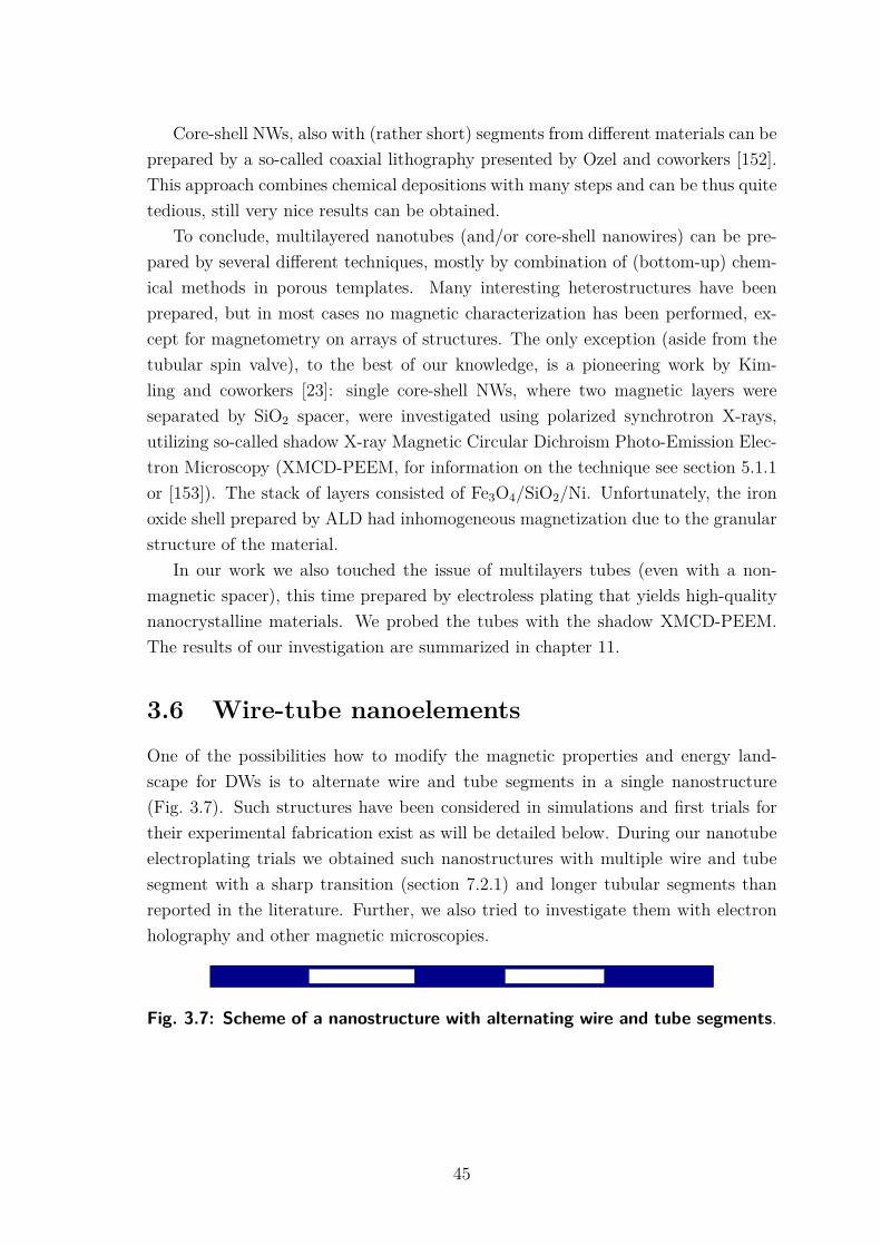
Core-shell NWs, also with (rather short) segments from different materials can beprepared by a so-called coaxial lithography presented by Ozel and coworkers [152].This approach combines chemical depositions with many steps and can be thus quitetedious, still very nice results can be obtained.
To conclude, multilayered nanotubes (and/or core-shell nanowires) can be pre-pared by several different techniques, mostly by combination of (bottom-up) chem-ical methods in porous templates. Many interesting heterostructures have beenprepared, but in most cases no magnetic characterization has been performed, ex-cept for magnetometry on arrays of structures. The only exception (aside from thetubular spin valve), to the best of our knowledge, is a pioneering work by Kim-ling and coworkers [23]: single core-shell NWs, where two magnetic layers wereseparated by SiO2 spacer, were investigated using polarized synchrotron X-rays,utilizing so-called shadow X-ray Magnetic Circular Dichroism Photo-Emission Elec-tron Microscopy (XMCD-PEEM, for information on the technique see section 5.1.1or [153]). The stack of layers consisted of Fe3O4/SiO2/Ni. Unfortunately, the ironoxide shell prepared by ALD had inhomogeneous magnetization due to the granularstructure of the material.
In our work we also touched the issue of multilayers tubes (even with a non-magnetic spacer), this time prepared by electroless plating that yields high-qualitynanocrystalline materials. We probed the tubes with the shadow XMCD-PEEM.The results of our investigation are summarized in chapter 11.
3.6 Wire-tube nanoelements
One of the possibilities how to modify the magnetic properties and energy land-scape for DWs is to alternate wire and tube segments in a single nanostructure(Fig. 3.7). Such structures have been considered in simulations and first trials fortheir experimental fabrication exist as will be detailed below. During our nanotubeelectroplating trials we obtained such nanostructures with multiple wire and tubesegment with a sharp transition (section 7.2.1) and longer tubular segments thanreported in the literature. Further, we also tried to investigate them with electronholography and other magnetic microscopies.
Fig. 3.7: Scheme of a nanostructure with alternating wire and tube segments.
45
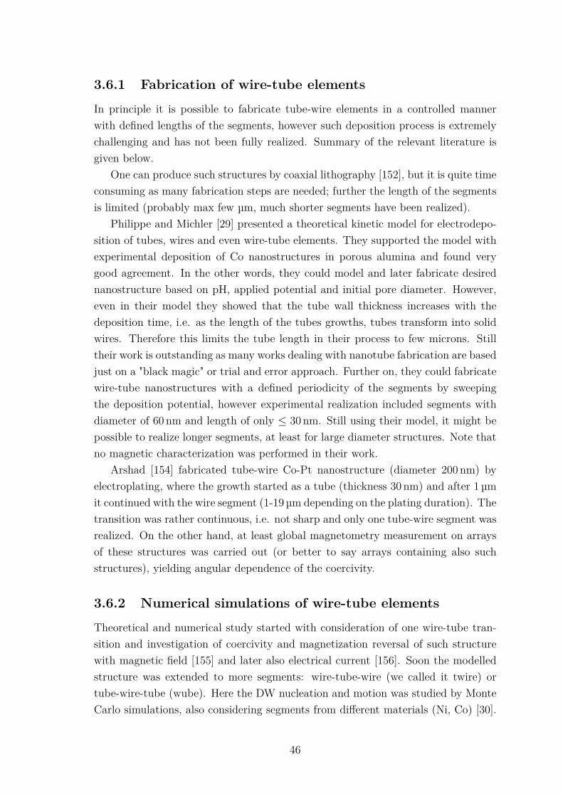
3.6.1 Fabrication of wire-tube elements
In principle it is possible to fabricate tube-wire elements in a controlled mannerwith defined lengths of the segments, however such deposition process is extremelychallenging and has not been fully realized. Summary of the relevant literature isgiven below.
One can produce such structures by coaxial lithography [152], but it is quite timeconsuming as many fabrication steps are needed; further the length of the segmentsis limited (probably max few µm, much shorter segments have been realized).
Philippe and Michler [29] presented a theoretical kinetic model for electrodepo-sition of tubes, wires and even wire-tube elements. They supported the model withexperimental deposition of Co nanostructures in porous alumina and found verygood agreement. In the other words, they could model and later fabricate desirednanostructure based on pH, applied potential and initial pore diameter. However,even in their model they showed that the tube wall thickness increases with thedeposition time, i.e. as the length of the tubes growths, tubes transform into solidwires. Therefore this limits the tube length in their process to few microns. Stilltheir work is outstanding as many works dealing with nanotube fabrication are basedjust on a "black magic" or trial and error approach. Further on, they could fabricatewire-tube nanostructures with a defined periodicity of the segments by sweepingthe deposition potential, however experimental realization included segments withdiameter of 60 nm and length of only ≤ 30 nm. Still using their model, it might bepossible to realize longer segments, at least for large diameter structures. Note thatno magnetic characterization was performed in their work.
Arshad [154] fabricated tube-wire Co-Pt nanostructure (diameter 200 nm) byelectroplating, where the growth started as a tube (thickness 30 nm) and after 1 µmit continued with the wire segment (1-19 µm depending on the plating duration). Thetransition was rather continuous, i.e. not sharp and only one tube-wire segment wasrealized. On the other hand, at least global magnetometry measurement on arraysof these structures was carried out (or better to say arrays containing also suchstructures), yielding angular dependence of the coercivity.
3.6.2 Numerical simulations of wire-tube elements
Theoretical and numerical study started with consideration of one wire-tube tran-sition and investigation of coercivity and magnetization reversal of such structurewith magnetic field [155] and later also electrical current [156]. Soon the modelledstructure was extended to more segments: wire-tube-wire (we called it twire) ortube-wire-tube (wube). Here the DW nucleation and motion was studied by MonteCarlo simulations, also considering segments from different materials (Ni, Co) [30].
46

Further work included simulations of coercivity and remanence as a function ofgeometry [157], later extended to full hysteresis loops and angular dependence ofmagnetic properties [158].
All previously mentioned works focused on isolated tubes; later magnetostaticinteractions between wire-tube nanostructures were considered – numerically for ahexagonal "array" of 7 nanostructures [159] and analytically for two elements [160].
47
Part II
Methods & Instrumentation
In this part we will rather briefly cover techniques used in experi-ments and numerical simulations. Experiments involve fabricationof samples, magnetic nanotubes, by bottom-up (electro)chemicalmethods using porous templates. Further, we cover their exper-imental investigation using a variety of techniques for structuraland magnetic characterization. Finally, we describe micromag-netic simulations of magnetization in tubes as well as numericalmodelling of contrast obtained by magnetic microscopies, both forcomparison and easier interpretation of the experimental images.
48

4 FABRICATION
In this section we will briefly cover the main electrochemical methods used for NTsynthesis – electroplating and electroless plating. Further, we will mention tem-plates used in order to get nanostructures of defined diameter (and length in case ofelectroless deposition). Last but not least, we feature atomic layer deposition, usedmainly for the template processing and partially also protection of the synthesisedNTs.
4.1 Templates
In order to obtain nanostructures of well-defined shape, we used templates withcylindrical holes (pores); namely we employed nanoporous alumina (mostly for elec-troplating) and porous track-etched polycarbonate (see Fig. 4.1). Both lab-madeand commercial templates were employed. Alumina membranes were fabricated bythe classical two-step anodization process [116] either by the author, or LaurentCagnon. We utilized also commercial templates from SmartMembranes. Polycar-bonate templates were used mainly for electroless plating and they will be furtherdescribed in section 4.4.1. A brief summary of some advantages and drawback ofboth template types is given below after few words on fabrication of templates.
4.1.1 Fabrication of templates
Nanoporous alumina is prepared by electrochemical anodic oxidation of high purityAl sheets (best annealed with low roughness – mechanically and electrochemicallypolished) in acidic solutions. Under certain conditions (acid, concentration/pH,applied voltage) aluminium oxide with hexagonally ordered straight nanoholes canbe obtained directed by the hydrogen evolution, volume expansion of the oxide andrelated stress and electrical field strength. Ordering can be improved by a patterningthe Al substrate or by Al reanodization after etching out the previously formed layer.It also improves with the anodizing time: the initial layer is disordered (and poremight be branched – see Fig. 7.7) as the pores nucleate at local defects and onlyafter certain time (pore length) the self-ordering is achieved. The pore diameter andspacing is almost linearly proportional to the applied voltage and the diameter canbe adjusted by chemical etching or atomic layer deposition of alumina inside thepores. Thickness of the membrane can range from hundreds of nanometres to tensof micrometres depending on the anodization time and the Al substrate. Voltagecan be changed during the growth leading to diameter modulations of the pores. Bya particular substrate patterning one can also get pores with triangular, rectangular
49

cross-section, provided that they are not too long (otherwise more natural cylindricalpores are recovered). More info can be found in book Nanoporous alumina [161].
Fabrication of polycarbonate templates is further discussed in section 4.4.1.Therefore, we mention here only the basic principle. Accelerated high energy ions(particles) are passed through a polycarbonate sheet (thickness typical in microme-ters). Ion tracks through the material make it less chemically resistant. Therefore,upon immersion of such treated sheet into strong basis (NaOH, KOH), one can etchpores. The pore size depends on the nature of the ions and their energy, etchant,and the etching time. Pore density is proportional to the fluence of ions and itsis in most cases lower than for as prepared alumina membranes. Usually, a widebeam of ions from a laboratory source is not perfectly collimated (typical irradiatedsurface area is at least several cm2) which leads to pores that are not straight andthat do not point in the same direction. Higher quality templates can be obtainedexploiting ions from large scale ion/particle accelerators.
Porous alumina vs ion track-etched polycarbonate
Polycarbonate membranes can be very easily and rapidly dissolved in e.g. dichloro-methane (within seconds). Such solvent does not oxidize the fabricated magneticnanostructures. From our experience it is also easier to obtain cleaner sample usingthese templates, i.e. with smaller amount of impurities coming mainly from templatedissolution residues. This is of particular importance for synchrotron experimentsperformed under ultra-high vacuum and high voltage applied between the sampleand microscope objective (such as in X-ray photoemission electron microscopy).Further, preparation and handling of membranes with thickness of several micronsdoes not rise a significant problem. The main drawback is a small temperaturestability window – this limits processing and measurement of NTs that are stillin the template. Further, especially commercial membranes have a quite roughsurface that translates into poor surface quality of the deposited nanostructures. Inaddition, other defects can occur: pores are not straight and sometimes intersectother pores.
The main advantage of nanoporous alumina is the hexagonally-ordered array ofstraight pores and possibility to engineer the template parameters: both diameterand pore spacing (pitch) can be controlled and adjusted almost independently. Inaddition, one can have pores with different diameters along their length which alsotranslates into deposited nanotubes/nanowires. In particular, one can create di-ameter modulations, protrusions, and constrictions in order to tune the magneticproperties and create nucleation and pinning sites for magnetic domain walls. Filledalumina membranes can withstand a wide range of temperatures from liquid helium
50
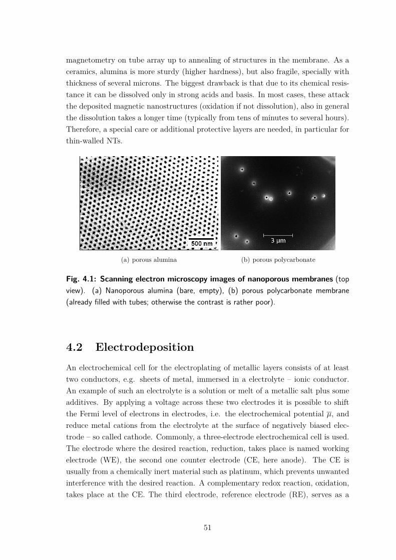
magnetometry on tube array up to annealing of structures in the membrane. As aceramics, alumina is more sturdy (higher hardness), but also fragile, specially withthickness of several microns. The biggest drawback is that due to its chemical resis-tance it can be dissolved only in strong acids and basis. In most cases, these attackthe deposited magnetic nanostructures (oxidation if not dissolution), also in generalthe dissolution takes a longer time (typically from tens of minutes to several hours).Therefore, a special care or additional protective layers are needed, in particular forthin-walled NTs.
(a) porous alumina (b) porous polycarbonate
Fig. 4.1: Scanning electron microscopy images of nanoporous membranes (topview). (a) Nanoporous alumina (bare, empty), (b) porous polycarbonate membrane(already filled with tubes; otherwise the contrast is rather poor).
4.2 Electrodeposition
An electrochemical cell for the electroplating of metallic layers consists of at leasttwo conductors, e.g. sheets of metal, immersed in a electrolyte – ionic conductor.An example of such an electrolyte is a solution or melt of a metallic salt plus someadditives. By applying a voltage across these two electrodes it is possible to shiftthe Fermi level of electrons in electrodes, i.e. the electrochemical potential 𝜇, andreduce metal cations from the electrolyte at the surface of negatively biased elec-trode – so called cathode. Commonly, a three-electrode electrochemical cell is used.The electrode where the desired reaction, reduction, takes place is named workingelectrode (WE), the second one counter electrode (CE, here anode). The CE isusually from a chemically inert material such as platinum, which prevents unwantedinterference with the desired reaction. A complementary redox reaction, oxidation,takes place at the CE. The third electrode, reference electrode (RE), serves as a
51

reference for measurement of the WE electrical potential. For more information onelectroplating and electrochemistry in general consult references [162, 163].
To get cylindrical nanostructures we used nanoporous alumina templates. Thetemplate itself is (and needs to be) an electrical insulator. The bottom side of thetemplate (with more ordered pores) is covered with an evaporated Au layer (witha 3-5 nm thick Ti seed layer) that serves as the WE. Therefore, the nanostructuresgrow from the bottom. Typically electroplating in such pores covered with thickcompact electrode yields solid nanowires. To promote the tube growth, the Au layeris so thin (with respect to the pore diameter) that it does not completely cover thepore opening [122, 123]. I.e. at the pore extremity it forms an annulus and not asolid disk. The Au side of the template is attached to a larger Cu plate, contact beingmade with an Agar silver paint (AGG302, Agar Scientific). Unwanted deposition ofmetals is avoided by covering other areas with chemically-resistant insulating tape(e.g. Kapton; non-conductive resin can be applied as well). For the electrochemicalcell setup and scheme of the working electrode see Figure 4.2.
Cu
Au
Nonconductive template
Nonconductive seal
template with Au (bottom)
b)
c)
Au
a)
Ag
Nonconductive seal
Fig. 4.2: Electroplating of tubes in nanopores. a) Scheme of an electrochemicalcell for plating in nanopores. The only contact of a plating solution with the workingelectrode should be through the pores. This requires either electrical insulation of therest of the electrode, or exposition of only one side of the electrode. Otherwise a filmwould be deposited on the backside of the electrode. b) Bottom view of a poroustemplate covered with thin layer of Au serving. Dashed circles show the pore position.Therefore, there pores are not completely closed with the Au layer (there is Au annulusinstead of disk at the bottom of each pore). c) Scheme of the template attached to Cumacro-electrode.
All our depositions were conducted at ambient conditions and room temperature.As the external current source we used a VersaSTAT 3 potentiostat (PrincetonApplied Research), the electrodes are summarized below:
52

• working electrode: porous Au layer at the bottom of a nanoporous template(alumina, polycarbonate),
• counter electrode: platinum mesh (higher surface area than the workingelectrode),
• reference electrode: saturated calomel electrode (SCE).Further details will be given in the following sub-sections dealing with particular
depositions. We will focus only on the depositions that are discussed in the resultssection: preparation of NiCo NTs (section 7.1) and Ni wire-tubes (section 7.2.1).Aside from these, we also tried Ni/Cu co-deposition with phase separation (Ni shelland Cu core) [129] and electrodeposition of Ni tubes via current pulses [164], but inthese cases, we obtained at best only few poor tubes with high roughness. Last butnot least, we tested also NiFe NT plating according to Zhang [165], but we obtainednanowires instead of nanotubes.
4.2.1 Ni wire-tube elements
Similar to Proenca’s work [123] we used a nanoporous alumina template; in ourcase commercial SmartPor50 (SmartMembranes) with pore diameter around 50 nm.However, several slight changes were employed. First, we evaporated 50 nm of Au(3 nm Ti seed layer) instead of 40 nm to serve as the porous working electrode.Further, the electrode was sealed at the bottom with a non-conductive tape insteadof a resin (see Fig. 4.2). Without such a sealing the yield of tubes is smaller: first, theelectrolyte can interact with the silver paint and decrease the adhesion and electricalcontact with the underlying Cu macro-electrode. Second, the penetration of theelectrolyte below the porous Au layer leads to deposition of continuous magneticfilm that eventually closes the holes in the Au layer and may lead to deposition ofsolid wires instead of tubes. Electrical contact was made at the sample Au electrodeedges with the silver paint. The deposition was conducted at room temperature(instead of 35∘C) at −1.55 V vs SCE for 20 min without any stirring (instead of250 RPM). The electrolyte, Watts bath, consisted of 1.14 M NiSO4, 0.19 M NiCl2,and 0.73 M H3BO3. Note that Proenca reported only deposition of nanowires, ornanotubes, i.e. no wire-tube elements.
4.2.2 NiCo nanotubes
We tried CoNi NT electrodeposition following the work by Zhang [166]. We useda lab-made nanoporous alumina template with the pore diameter 80-90 nm. Wedeposited a thin porous electrode (3 nm Ti + 10 nm Au) on the bottom side of thetemplate by electron beam evaporator. Further, we sealed the bottom of the porous
53

electrode with Kapton tape. The electroplating was conducted at room temperature,−2.0 V vs SCE for 30 min. We used a fresh electrolyte with pH 2.5 with the followingcomposition: 0.05 M CoSO4, 0.05 M NiSO4, and 0.1 M H3BO3.
4.3 Atomic layer deposition
Atomic Layer Deposition (ALD) [131, 132] was used for deposition of thin oxidelayers, mainly AlO𝑥 and HfO𝑥, serving as a mechanical reinforcement of NTs, aprotective layer, and as a non-magnetic spacer in trials for deposition of multilayeredtubes. Further, we used it also for the reduction of the pore diameter of the aluminatemplates. We utilized Savannah ALD (Cambridge NanoTech). Note that most ofour tubes were without protective ALD coating as our main investigation methodis based on emission of photoelectrons from the sample surface and additional non-conductive layer can decrease their yield and lead to electric charging effects.
4.4 Electroless plating
Electroless plating (autocatalytic deposition) relies on the reduction of metallic ionsfrom the liquid electrolyte by means of a reducing agent – chemical substance provid-ing electrons for the reduction. Unlike in electroplating, no external current sourceis needed and samples do not have to be electrically conductive. Therefore, almostany surface can be coated, even though some (e.g. non-conductive ones) may haveto be chemically modified – using so called sensitization and activation proceduresdescribed below. Further, the deposition is conformal like in case of atomic layerdeposition and high-aspect ratio structures (pillars, nanopores) can be covered withthe deposit. A large variety of materials can be deposited: metals, alloys, metalloids,oxides, . . . Being based on a rather simple "beaker" chemistry and owing to its ver-satility, the technique is used in industry, particularly in microelectronics. Furtherinformation on electroless plating can be found in references [162, 167, 168].
The choice of the reducing agent depends on the metal to be plated as well ason the chemical resistance of the substrate. Many reducing agents contain boron(e.g. dimethylamino borane – our case) or phosphorous (sodium hypophosphite).A portion (from few to tens of percent) of these elements is incorporated in thedeposit and by changing their content, many material properties can be influenced(grain size, electrical conductivity, hardness, . . . ). Amount of B (P) depends on thedeposition process, mainly on the pH and reducing agent concentration. Almostpure metals can be obtained using hydrazine or formaldehyde.
54
The method has been also employed for magnetic (nano)tube fabrication [127–129]. The technique provides good control over the tube thickness [130] (proportionalto the plating time), diameters down to 100 nm using porous templates [19] and50 nm in case of biotemplates [113]. The grain size of the deposit can be decreasedupon increase of the B or P content ([169], p. 122).
We used tubes prepared by this method in most of our experiments. First werelied on a supply of tubes from Sandra Schaefer in TU Darmstadt (samples labelledwith SS, consult Tab. 4.1), later we fabricated also our own NTs following the sameprocedure.
Tab. 4.1: Survey of electroless-deposited samples from TU Darmstadt. Only samplesused in our work are featured.
Sample Diameter Length DescriptionSS53 300 nm ≤30 µm CoNiB tubesSS123 390 nm ≤30 µm NiFeB tubesSS124 150 nm ≤10 µm CoNiB tubesSS125 100 nm ≤10 µm CoNiB tubesSS126 80 nm ≤10 µm CoNiB tubesSS147 400 nm ≤20 µm multilayered tubes: NiFeB/(Pd)/CoNiBSS148 400 nm ≤20 µm multilayered tubes: NiFeB/SnO𝑥/CoNiB
4.4.1 Templates
As a shape-giving template, ion-track etched polycarbonate membranes were used.The track formation and track etching process is explained in literature [115]. Forall the samples denotated with SS (fabricated by Sandra Schaefer) lab-made tem-plates were prepared as follows. A polycarbonate foil (Pokalon from LOFO, HighTech Film GmbH) was irradiated with Au26+ ions at the GSI Helmholtzzentrum fürSchwerionenforschung GmbH (Darmstadt). An example of irradiation parametersfor 300 nm pore diameter follows: fluence 107 ions/cm2; kinetic energy of the pro-jectile 11.4 MeV per nucleon. The latent ion tracks were etched out at 50∘C in a6M stirred sodium hydroxide solution. The etching time was adjusted dependingon the desired pore diameter, 11 min were used for pore size around 300 nm (sampleSS53). The as-prepared templates with cylindrical pores were washed with waterand dried. The length of the tubes is determined by the template thickness (porelength); for smaller pore size (80-150 nm) we used mainly 10 µm-thick foils, whereasfor larger pores (300-400 nm) we employed templates with thickness of 20 or even
55

30 µm. Thus, for smaller pores we used smaller template thickness as plating inhigher aspect ratio pores is more challenging.
In some cases, we observed a narrowing of the pore diameter close to the templatesurfaces, which led to cigar shaped structures upon filling the template. This effectoccurs when the irradiated polycarbonate film is not etched directly after irradiation,but after some time (months). Ageing results in partial "healing" of the polymer andmodifications that are more pronounced close to the template surface. Modificationsmake the pore ends more resistant to the chemical etching resulting in narrowerdiameters.
For the samples synthesized at Institut Néel (see section 7.3), we used commer-cial templates Osmonics Poretics (K01CP01300) with the following characteristics:nominal pore diameter 0.1 µm, membrane thickness ≤ 7 µm, and 1.5 ·108 pores/cm2.Such porosity is still rather large and may result in unwanted defects (e.g. inter-secting pores).
One can also employ nanoporous alumina templates, the electroless plating pro-cedure is basically the same as for polycarbonate (see below), except that at thebeginning the pore walls are modified with e.g. 3-AminoPropylTriEthoxySilane(APTES) [129]. We successfully performed tests of such depositions, consult Fig. 7.7.
4.4.2 Fabrication procedure
The deposition of NTs inside porous polycarbonate membranes consists of severalsteps. First, the porous template is sensitized with a SnCl2 solution (42 mM SnCl2and 71 mM trifluoroacetic acid in 1:1 methanol:water) and activated with a PdCl2solution (11.3 mM PdCl2, 33.9 mM KCl) [127]. The goal of the activation procedureis to bind tiny Pd particles (less than few nm in size) on the pore walls that willcatalyse the deposition of the desired material (metal). The procedure (sensitizationfollow by the activation) is repeated three times in order to obtain better surfacecoverage with the Pd particles (poor coverage could lead to holes and increase inroughness of the deposited layer). After the three cycles of sensitization (45 min first,then only 15 min each) plus activation (4 min each cycle), the template is washedwith ethanol and water, then immersed in the electroless plating bath. The depo-sition takes place at room temperature. It starts at the pore walls on the catalyticPd seed particles and continues radially towards the pore centre (Fig. 4.3). Duringthe synthesis, hydrogen gas evolves at the template surface as a part of the depo-sition reaction. The composition of plating solutions for various materials (metals)is given below. In general, it consists of the metal source (metallic salt), reducingagent, and additives: pH buffers keeping the same (very similar) acidity/alkalinityof the solution; complexing agents – partially binding metallic ions and increasing
56
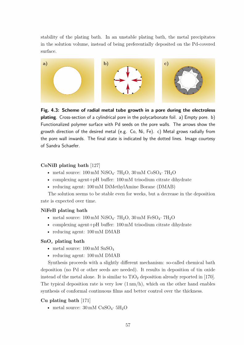
stability of the plating bath. In an unstable plating bath, the metal precipitatesin the solution volume, instead of being preferentially deposited on the Pd-coveredsurface.
a) b) c)
Fig. 4.3: Scheme of radial metal tube growth in a pore during the electrolessplating. Cross-section of a cylindrical pore in the polycarbonate foil. a) Empty pore. b)Functionalized polymer surface with Pd seeds on the pore walls. The arrows show thegrowth direction of the desired metal (e.g. Co, Ni, Fe). c) Metal grows radially fromthe pore wall inwards. The final state is indicated by the dotted lines. Image courtesyof Sandra Schaefer.
CoNiB plating bath [127]• metal source: 100 mM NiSO4· 7H2O, 30 mM CoSO4· 7H2O• complexing agent+pH buffer: 100 mM trisodium citrate dihydrate• reducing agent: 100 mM DiMethylAmine Borane (DMAB)The solution seems to be stable even for weeks, but a decrease in the deposition
rate is expected over time.
NiFeB plating bath• metal source: 100 mM NiSO4· 7H2O, 30 mM FeSO4· 7H2O• complexing agent+pH buffer: 100 mM trisodium citrate dihydrate• reducing agent: 100 mM DMAB
SnO𝑥 plating bath• metal source: 100 mM SnSO4
• reducing agent: 100 mM DMABSynthesis proceeds with a slightly different mechanism: so-called chemical bath
deposition (no Pd or other seeds are needed). It results in deposition of tin oxideinstead of the metal alone. It is similar to TiO2 deposition already reported in [170].The typical deposition rate is very low (1 nm/h), which on the other hand enablessynthesis of conformal continuous films and better control over the thickness.
Cu plating bath [171]• metal source: 30 mM CuSO4· 5H2O
57

• complexing agent: 35 mM EthyleneDiamineTetraacetic Acid (EDTA)• pH buffer: 380 mM TriEthanolAmine (TEA)• reducing agent: 100 mM DMABDespite EDTA being a strong complexing agent, the bath is not very stable and
Cu precipitates in the solution within few hours, therefore a fresh solution shouldbe used. Stability could be increased by increasing the EDTA concentration andit should also depend on the pH. Different recipes using formaldehyde or sodiumborohydride as the reducing agent exist as well.
4.4.3 Multilayered tubes
Multilayered tubes were prepared by Sandra Schaefer (TU Darmstadt) using sub-sequent deposition of different layers. In general, one has to keep in mind that thechemistry used for the synthesis of a new layer may modify (or even attack) theprevious layer(s), which may restrict the choice of materials.
We summarize the steps for fabrication of SS148 NiFeB/SnO𝑥/CoNiB trilayeredtubes in Fig. 4.4.
Fig. 4.4: Scheme of the preparation process for the multilayered tubes (hereSS148 NiFeB/SnO𝑥/CoNiB). Porous membrane is first sensitized and activated (3×) andsubsequently it is immersed in different aqueous solutions. After deposition of each layer,film formed on top/bottom part of the membrane is removed by a gentle mechanicalpolishing. Image courtesy of Sandra Schaefer.
SS147 with a Pd spacer was prepared in a similar way, just the CoNiB depositionis longer (65 min as the deposition rate appeared to be lower) and the oxide spacerdeposition is replaced by Pd plating procedure as follows:
Pd plating bath [172]• metal source: 4 mM PdCl2
58
• complexing agent+ligand: 38 mM pentane-2,4-dione (acetylacetonate),47 mM 4-(DiMethylAmino)Pyridine (DMAP)
• reducing agent: 80 mM hydrazine monohydrateThe bath was heated to 50∘C and the polycarbonate membrane with NiFeB
tubes was immersed in the solution for 1 h. As the reaction rate seemed to be slow,the temperature was raised to 70∘C and the deposition run for another 1 h.
4.5 Sample preparation for measurements
After the nanostructure deposition in templates, the template is washed with dem-ineralized water and dried. The metallic film deposited on the top/bottom surfacesof the template is removed by a gentle mechanic polishing using a fine sand paper.For measurements requiring isolated tubes, the polycarbonate template is dissolvedin dichloromethane and the tubes are rinsed several times (at least 3 times) withthe same solvent. Alumina membranes are dissolved (as mentioned above) in 1 Msodium hydroxide and rinsed with water (3× or more) and then isopropyl alcohol(3× or more). Typically, a piece of a template with area of few mm2 is immersed in0.5 mL of the etchant. The insufficiently rinsed structures are later (after dispersionon a substrate)) covered with rest of the template dissolution process. Depend-ing on the measurement technique, the tubes are dispersed either on a doped Sisubstrate with alignment marks (for XMCD-PEEM, magnetic force microscopy ormagnetooptics with focused laser), or on a Cu grid with a thin lacey carbon film (fortransmission electron microscopies and electron holography) or on a 100 nm-thickSiN membrane (for scanning transmission X-ray microscopy). For the dispersion,several µL are (repeatedly) transferred onto the substrate using a micropipette. Foralignment of the tubes we insert a permanent magnet below the substrate with thefield direction colinear with the airflow inside the hood. For a set of orthogonaltubes (Fig. 4.5b), the process is done twice with substrate rotation by 90∘ vs themagnet and in both cases with weak airflow 45∘ to the field direction. Images of thetubes on some of these substrates can be found in section 5.1.3.
59
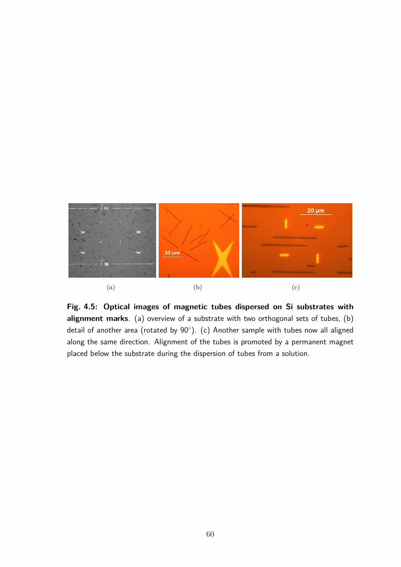
(a) (b) (c)
Fig. 4.5: Optical images of magnetic tubes dispersed on Si substrates withalignment marks. (a) overview of a substrate with two orthogonal sets of tubes, (b)detail of another area (rotated by 90∘). (c) Another sample with tubes now all alignedalong the same direction. Alignment of the tubes is promoted by a permanent magnetplaced below the substrate during the dispersion of tubes from a solution.
60
5 CHARACTERIZATION
In this chapter we will describe shortly the techniques used for magnetic, struc-tural, and topographical characterization of the samples. Aside from electron mi-croscopy, related analytic techniques and electron holography, we cover synchrotronobservations with circularly polarized X-ray beam, scanning probe microscopy, andmagnetometry.
In the majority of the magnetic measurements the samples were AC demagne-tized in a transverse direction (vs tube axis) before imaging. In case of VSM-SQUIDsample was demagnetizated along the direction of field applied during acquisition ofthe hysteresis loops.
5.1 Synchrotron X-ray microscopies
For the determination of magnetization in our tubes we utilize mainly synchrotron-based magnetic microscopies relaying on X-ray Magnetic Circular Dichroism (XMCD),a difference in absorption for left and right circularly-polarized light. Aside fromthe helicity (circular polarization) of the photons (carrying thus angular momen-tum), the absorption depends on the sample magnetization with respect to thebeam propagation direction. For iron group elements the effect is strong at the L3
and L2 absorption edges (See Fig. 5.1a).The effect can be detected either in a direct transmission of photons (scanning or
wide-field transmission X-ray microscopy) or via collection of photoelectrons (pho-toemission electron microscopy – PEEM) – see Fig. 5.2. The amount of createdphotoelectrons is assumed to be proportional to the absorbed photons (of sufficientenergy). In case of very thin films, the photoelectron yield is proportional to theabsorption, however, for thicker samples only a part of photoelectrons can leave thesample and contribute to the detected signal. In our experimental study we utilizemostly the X-PEEM technique.
The XMCD microscopies are element sensitive, in our work we focus on L3
and L2 absorption edges of transition metals forming our ferromagnetic tubes –mostly Co and Fe (Ni gives usually a weaker XMCD contrast even if the sampleis Ni-rich due to the smaller number of holes in the absorption band). As theprecise energy of the absorption edge can differ (even up to a few eV) from sampleto sample (even among tubes on the same substrate) due to local environment ofthe probed atoms (e.g. degree of oxidation), one usually start with determiningthe edge energy via X-ray Absorption Spectroscopy (XAS). Further, there mightbe instrument (calibration) related energy shift. In XAS, the energy of the beamis scanned while we monitor the photon absorption (or photoelectron yield). In
61
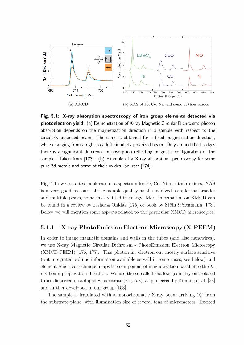
(a) XMCD (b) XAS of Fe, Co, Ni, and some of their oxides
Fig. 5.1: X-ray absorption spectroscopy of iron group elements detected viaphotoelectron yield. (a) Demonstration of X-ray Magnetic Circular Dichroism: photonabsorption depends on the magnetization direction in a sample with respect to thecircularly polarized beam. The same is obtained for a fixed magnetization direction,while changing from a right to a left circularly-polarized beam. Only around the L-edgesthere is a significant difference in absorption reflecting magnetic configuration of thesample. Taken from [173]. (b) Example of a X-ray absorption spectroscopy for somepure 3d metals and some of their oxides. Source: [174].
Fig. 5.1b we see a textbook case of a spectrum for Fe, Co, Ni and their oxides. XASis a very good measure of the sample quality as the oxidized sample has broaderand multiple peaks, sometimes shifted in energy. More information on XMCD canbe found in a review by Fisher & Ohldag [175] or book by Stöhr & Siegmann [173].Below we will mention some aspects related to the particular XMCD microscopies.
5.1.1 X-ray PhotoEmission Electron Microscopy (X-PEEM)
In order to image magnetic domains and walls in the tubes (and also nanowires),we use X-ray Magnetic Circular Dichroism - PhotoEmission Electron Microscopy(XMCD-PEEM) [176, 177]. This photon-in, electron-out mostly surface-sensitive(but integrated volume information available as well in some cases, see below) andelement-sensitive technique maps the component of magnetization parallel to the X-ray beam propagation direction. We use the so-called shadow geometry on isolatedtubes dispersed on a doped Si substrate (Fig. 5.3), as pioneered by Kimling et al. [23]and further developed in our group [153].
The sample is irradiated with a monochromatic X-ray beam arriving 16∘ fromthe substrate plane, with illumination size of several tens of micrometers. Excited
62

Scanning TransmissionX-ray Microscopy
X-ray PhotoEmissionElectron Microscopy
Photoelectrons
Photoelectrons
Aperture
Monochromatic X-rays
MonochromaticX-rays
Sample
Scanning
stagesample
Phosphorscreen
Magnified image
Projectionlens
Objectivelens
X-raydetector
Zone platefocusing lens
FluorescencePhotons
Fig. 5.2: Magnetic X-ray microscopies: Taken from [175] (original image is in [173]).
X-raysShadow
Sample
Si substrate
Photoelectrons
Fig. 5.3: Shadow XMCD-PEEM scheme. X-rays with energy matching the absorp-tion edge of the sample (e.g. Co-L3 for Co-rich sample) arrive 16∘ from the supportingSi substrate. The photons are absorbed and emit photoelectrons. This happens mainlyat the sample (e.g. tube) surface (resonant absorption). Absorption of photons leadsto creation of a geometrical shadow behind the sample. If the sample is not too thick(maximum few hundreds of nanometres depending on the material and X-ray energy),some photons are transmitted through the sample; these photons create additional pho-toelectrons upon being absorbed by the supporting substrate (non-resonant absorption)in the shadow area. Other parts of the substrate irradiated by the X-rays also emitphotoelectrons (but smaller amount than the sample surface).
63
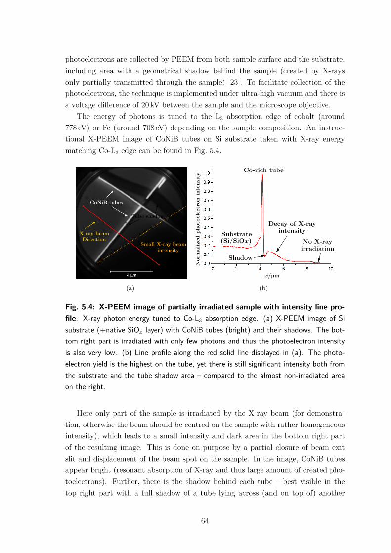
photoelectrons are collected by PEEM from both sample surface and the substrate,including area with a geometrical shadow behind the sample (created by X-raysonly partially transmitted through the sample) [23]. To facilitate collection of thephotoelectrons, the technique is implemented under ultra-high vacuum and there isa voltage difference of 20 kV between the sample and the microscope objective.
The energy of photons is tuned to the L3 absorption edge of cobalt (around778 eV) or Fe (around 708 eV) depending on the sample composition. An instruc-tional X-PEEM image of CoNiB tubes on Si substrate taken with X-ray energymatching Co-L3 edge can be found in Fig. 5.4.
CoNiB tubes
Tube shadow
Small X-ray beamintensity
X-ray beamDirection
(a)
x/µm
Norm
alize
dphoto
electro
nintensity
Shadow
Substrate(Si/SiOx)
Co-rich tube
Decay of X-rayintensity
No X-rayirradiation
(b)
Fig. 5.4: X-PEEM image of partially irradiated sample with intensity line pro-file. X-ray photon energy tuned to Co-L3 absorption edge. (a) X-PEEM image of Sisubstrate (+native SiO𝑥 layer) with CoNiB tubes (bright) and their shadows. The bot-tom right part is irradiated with only few photons and thus the photoelectron intensityis also very low. (b) Line profile along the red solid line displayed in (a). The photo-electron yield is the highest on the tube, yet there is still significant intensity both fromthe substrate and the tube shadow area – compared to the almost non-irradiated areaon the right.
Here only part of the sample is irradiated by the X-ray beam (for demonstra-tion, otherwise the beam should be centred on the sample with rather homogeneousintensity), which leads to a small intensity and dark area in the bottom right partof the resulting image. This is done on purpose by a partial closure of beam exitslit and displacement of the beam spot on the sample. In the image, CoNiB tubesappear bright (resonant absorption of X-ray and thus large amount of created pho-toelectrons). Further, there is the shadow behind each tube – best visible in thetop right part with a full shadow of a tube lying across (and on top of) another
64

tube. The shadow is brighter in its centre with confirms the hollow character of thetube. In most cases, a part of the shadow is obstructed by the tube (sample) itself.However, in principle tubes can be placed on a pre-patterned substrate (elevatednon-magnetic pads, e.g. from Au) in order to recover the full shadow.
The photoelectron intensity profile along the red line is shown in Fig. 5.4b. Theintensity is normalized to the maximum, obtained from the tube surface. Veryimportant fact for our magnetic imaging (as will be discussed below) is that thephotoelectron yield from the Si substrate is significant. Even-though the X-rayenergy is tuned for Co-L3 (around 778 eV), thus far away from both L and K edgesof Si, the non-resonant absorption of X-rays and subsequent photoelectron emissiongives about 20 % of photoelectron signal from the sample. In the geometrical shadowthis value is clearly smaller, yet still non-negligible compared to the part of thesample (bottom-right) that is not irradiated by the X-rays. To the right of the tube(in the profile) the photoelectron yield decays due to smaller amount of incomingX-ray photons (partially closed slit). Note again that for the proper imaging theX-ray beam must be centred on the point of interest and the X-ray irradiationshould be rather homogeneous across the whole region of interest (in such a case thephotoelectron signal from the substrate can be slightly smaller with respect to thetube).
In order to obtain the magnetic information, 2 (sets of) X-PEEM images areacquired, one for each circular polarization of the X-ray beam. The XMCD magneticimage is obtained as normalized difference of these two:
𝐼 − 𝐼�𝐼 + 𝐼�
. (5.1)
The resonant X-ray absorption of the sample (tube) depends on the polarizationand magnetization direction with respect to the beam propagation direction. Onthe other hand, the absorption of X-rays by the Si substrate does not depend onthe beam polarization. Thus in XMCD, the substrate does not contribute to themagnetic image and creates grey, non-magnetic background. However, there is oneexception: the shadow area on the substrate. While the substrate is non-magneticand its absorption of photons is independent of the beam polarization, the amount ofcreated photoelectrons does depend on the intensity of incoming X-ray photons. Andthis amount of photons transmitted through the sample (tube) depends on the beampolarization – for one circular beam polarization more X-ray photons are absorbedand thus less photons will hit the substrate behind the tube, i.e. in the shadowarea. Thus, the shadow reflects magnetic volumic information integrated along thephoton path. Due to the integration, the interpretation of magnetic contrast inthe shadow might not be as straight-forward as in the case of signal coming from
65
the tube surface. However, one can compare it with numerical modelling of the(shadow) XMCD-PEEM contrast that has been developed in our group [153]. Suchmodelling also enables in principle quantitative analysis of the images.
The XMCD-PEEM technique has a spatial resolution around 30-40 nm for themagnetic imaging (depends on sample and parameters). Note that in the shadowthe resolution is improved up to a factor of 3.6 (1/ sin 16∘) along the beam direction,because the shadow is stretched due to the small incidence angle of the beam.While XMCD-PEEM is basically surface-sensitive technique (photoelectrons havesmall energy and cannot escape from the sample/substrate volume), thanks to theshadow we can also (indirectly) obtain information on the magnetization in thevolume of the sample, in particular when comparing experimental XMCD-PEEMimages with numerical modelling for several micromagnetic configurations [153].
By tuning the focus point of the microscope (adjusting a current flowing throughthe objective lenses) and by optimizing a so-called start voltage (STV, an addi-tional voltage bias applied to the sample which determines the kinetic energy ofthe collected photoelectrons) one can focus either on the tube surface, shadow, ora comprise of both (depends also on the geometry – for larger tube diameter theintermediate focus will not be as good as clear focus on either tube, or the shadow).Further information can be found in reference [153].
Typically, for one resulting XMCD-PEEM image, 30-60 images are acquired forboth circular polarizations of the beam with acquisition time of few seconds foreach image in order to improve the signal to noise ratio. Stack of images for thesame polarization are drift-corrected, co-added (averaged), and finally two obtainedimages (one for each polarization) are again drift-corrected and the XMCD image iscalculated as their normalized difference. The amount of averaged images and theacquisition time is a compromise between high signal-to-noise ratio, low resultingimage blurring caused by sample drift (mainly mechanical) and total time needed forthe acquisition of images. The experiments were performed at the Nanospectroscopy(synchrotron Elettra) and HERMES (synchrotron SOLEIL) beamlines.
Annealing
The in-situ annealing was performed at Elettra under ultra-high vacuum, howeverin a chamber distinct from the X-PEEM microscope chamber (preparatory chamberconnected to the PEEM). We ramped the temperature to the desired value, keepingit at least for 30 min (except for 300∘C – only 10 min), and then we cooled the sampledown to room temperature. The annealing was repeated several times with gradualincrease in the target annealing temperature. The imaging was performed after eachannealing step. The temperature control was not very precise as we used a small
66

current-heated filament in the cartridge at the back of the sample. The temperaturewas estimated based on previous and similar filament heating experiments, and on acomparison with annealing of twin samples in a more controlled environment. Thisimplies an uncertainty of ±50∘C.
Application of magnetic field
Magnetic field was applied using a dedicated sample cartridge with a coil fitted in thecartridge below the sample. The coil is powered by an external current source thatenable either continuous operation or current pulses of duration in ms or longer. Thefield direction is always perpendicular to the X-ray beam due to the sample holderconstruction. During our first experiments with this setup, the magnetization of thesample could be switched with extremely low field values (< 0.1 mT). A detailedinspection and testing revealed that the problem was in the current source supplyingcurrent for the coil and the way it had been programmed. As the current source wasnot bi-directional, one had to switch the current leads to apply field in the oppositedirection. For this, the source was turned off as well as the high-voltage rack (remind:there is 20 kV between sample and the objective lenses of the microscope). Afterturning the source on again, during initialization, there was a current spike of about5 A (producing field around 100 mT) (see Fig. 5.5). Therefore, this spike reversedthe magnetization in the sample (magnetic NTs), the desired fields values appliedafterwards had thus no effect on the sample. The effect of this spike on azimuthalmagnetic domains in tubes is discussed in section 11.2.2.
The spike was later suppressed by reprogramming the supply by the beamlinescientists and reliable imaging after application of magnetic field (for 0.5 s or longer)or even in the magnetic field could be conducted. In the results section (experimentalresults) we will state whether spike or just DC field was applied.
We also performed imaging under applied magnetic field. In this case, the col-lected photoelectrons and thus the obtained image was affected by the field. Typ-ically upon increasing the field (in 1 mT steps) the field of view moved. We triedto compensate this by introducing additional electron beam shift, tuning stigmatorcoils, STV, etc. Both field and tweaking of the settings led to decrease of the sig-nal/noise and deterioration of the spatial resolution. Later we found out that it wassufficient to adjust excitation of the main objective lenses.
5.1.2 Scanning Transmission X-ray Microscopy (STXM)
This technique relies on the transmission of X-rays through a thin sample that mustbe placed on a thin, X-ray transparent substrate (in our case 100 nm-thick SiNmembrane). The X-ray beam is focused by diffractive Fresnel zone plate optics to a
67

0A
1A
2A
3A
4A
5A
20ms
(a) current spike (b) field cartridge
Fig. 5.5: X-PEEM field cartridge: current spike during electromagnet initial-ization. (a) Current spike before setting the desired current for the coil producingfield in XMCD-PEEM experiments. Photo courtesy of Andrea Locatelli. (b) Photo ofthe custom designed X-PEEM cartridge (Nanospectroscopy beamline, Elettra) with coilwindings. The sample is inserted on top of the pole pieces and covered with a metalliccap with a small opening (around 5 mm).
spot of 30 nm, which defines the resolution of the technique. Scanning by the sample(on piezo-stage) is performed in order to reconstruct pixel by pixel a larger image.Magnetic imaging relies again on XMCD at L3 edges. The contrast is very similarto the one obtained by XMCD-PEEM in the shadow. Imaging can be performedunder higher magnetic fields (typically hundreds of mT, even above 1 T possible)as we detect directly photons that are not affected by the field. We used STXMat the HERMES beamline to obtain images of CoNiB tubes under increasing axialmagnetic field to extract the strength of the anisotropy field related to the azimuthalanisotropy (section 8.3.1). Magnetic field is created by a set of 4 rotatable permanentrod magnets whose mutual orientation is controlled by motors. The setup enablesapplication of magnetic field up to 200 mT in the sample (substrate) plane.
5.1.3 Substrates for synchrotron experiments
For STXM, the tubes are dispersed on thin silicon nitride (Si3N4) membranes(100 nm or 200 nm), whose thick Si frames are glued onto a metallic plate – seeFig. 5.6. We tried both commercial membranes (window size 1.0 mm and thickness100 nm) provided by Synchrotron Soleil and lab-made substrates with Au alignmentmarks (window size 0.7 mm, thickness 200 nm, Au marks with thickness of 40 nm).
In case of XMCD-PEEM, we used larger n-doped Si substrates (up to 1 cm edge)with Au alignment marks such as shown in Fig. 4.5. The same substrates (and
68

5mm
Sample plate
Si 3N
4membra
ne
Si frame
(a) sample plate
SiSi3N4
Si
Si3N4
(b) membrane scheme
200µm
(c) custom Si3N4 + Au marks
Fig. 5.6: Si3N4 membranes for STXM. a) Photo of a metallic sample plate with themembrane (edge of the Si support frame is 5 mm), X-rays arrive perpendicular to theplane. b) Scheme of the Si3N4 membrane on the Si support frame (bottom and cross-section side view). c) Optical image (top view) of a custom-made Si3N4 membrane(Nanofab, Institut Néel) with Au (40 nm) alignment marks. The brighter inner squarehighlighted by the dashed red square corresponds to the membrane "window" (membraneedge 0.7 mm, thickness 200 nm). There are magnetic tubes dispersed on top of themembrane as well as many impurities from the template dissolution. These impurities(extreme case shown, cleaner samples with aligned tubes were used as well) are not anissue for STXM, however, for XMCD-PEEM such sample would be unusable.
69

sometimes also the same samples) were used for magnetic force microscopy andmagneto-optical measurements with focused laser. The substrates were designed byAlexis Wartelle and fabricated by Bruno Fernandez (Nanofab, Institut Néel).
5.2 Atomic & Magnetic force microscopy
Atomic Force Microscopy (AFM) senses interaction between sharp tip and a sample.The interaction is commonly detected through displacement or change in oscillation(amplitude, phase, frequency) of a microlever that bears the sharp tip. Aside fromshort-ranged van der Waals interaction providing basically the sample topography,one can employ a tip with a magnetic coating to probe magnetic longer-range inter-action as well.
More about AFM can be found in a very nice book by Eaton and West [178]. Forfurther information on Magnetic Force Microscopy (MFM) one can consult ([179],chapters 11 and 12), ([54], section 2.6.1) or author’s master thesis [180].
Two main instruments were used for the investigation of our samples: NT-MDTNtegra Aura (imaging under field possible) and HR-MFM Nanoscan (imaging undervacuum).
5.2.1 NT-MDT Ntegra Aura with Px controller
The Ntegra Aura microscope is specifically designed for magnetic force microscopy(no magnetic sample holder, no microscope parts affected by the field in the samplearea) and enables application of magnetic field during the imaging. One can useeither a standard commercial base with coils for in-plane field (up to approx 200 mT,pole pieces and gap dependent) and custom-made coils, or a dedicated home-madebase for measurement with out-of-plane magnetic field (even above 1 T).
Classical two pass tapping/lift mode technique introduced by Digital Instru-ments [181] was used for the imaging. During the first pass, the oscillation ampli-tude change was tracked showing (predominantly) the sample topography, whereasthe phase shift of the oscillating cantilever was recorded in the second pass at el-evated (lift) height, reflecting longer range interactions (mostly magnetic, but alsoelectrostatic).
5.2.2 HR-MFM Nanoscan
The microscope from Nanoscan dedicated to high resolution MFM imaging at Insti-tut Néel was operated under secondary vacuum (1 ·10−4 Pa) in order to benefit fromhigher sensitivity and (thermal) stability. The low pressure significantly increases
70
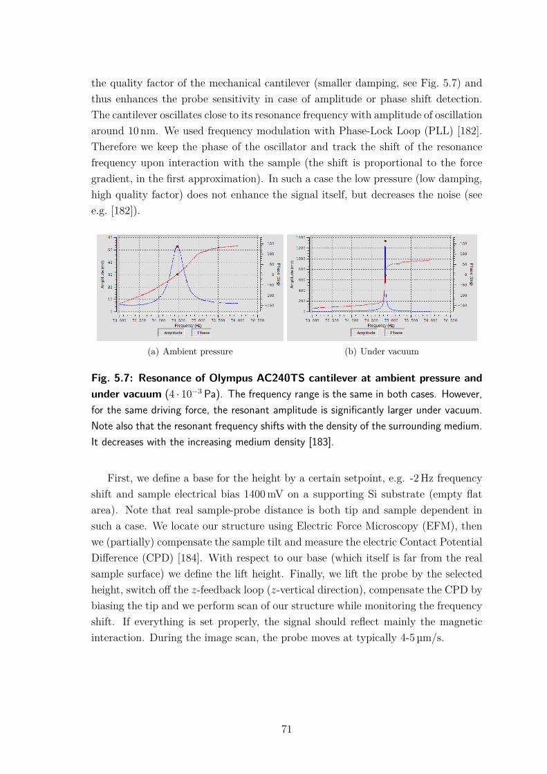
the quality factor of the mechanical cantilever (smaller damping, see Fig. 5.7) andthus enhances the probe sensitivity in case of amplitude or phase shift detection.The cantilever oscillates close to its resonance frequency with amplitude of oscillationaround 10 nm. We used frequency modulation with Phase-Lock Loop (PLL) [182].Therefore we keep the phase of the oscillator and track the shift of the resonancefrequency upon interaction with the sample (the shift is proportional to the forcegradient, in the first approximation). In such a case the low pressure (low damping,high quality factor) does not enhance the signal itself, but decreases the noise (seee.g. [182]).
(a) Ambient pressure (b) Under vacuum
Fig. 5.7: Resonance of Olympus AC240TS cantilever at ambient pressure andunder vacuum (4 · 10−3 Pa). The frequency range is the same in both cases. However,for the same driving force, the resonant amplitude is significantly larger under vacuum.Note also that the resonant frequency shifts with the density of the surrounding medium.It decreases with the increasing medium density [183].
First, we define a base for the height by a certain setpoint, e.g. -2 Hz frequencyshift and sample electrical bias 1400 mV on a supporting Si substrate (empty flatarea). Note that real sample-probe distance is both tip and sample dependent insuch a case. We locate our structure using Electric Force Microscopy (EFM), thenwe (partially) compensate the sample tilt and measure the electric Contact PotentialDifference (CPD) [184]. With respect to our base (which itself is far from the realsample surface) we define the lift height. Finally, we lift the probe by the selectedheight, switch off the 𝑧-feedback loop (𝑧-vertical direction), compensate the CPD bybiasing the tip and we perform scan of our structure while monitoring the frequencyshift. If everything is set properly, the signal should reflect mainly the magneticinteraction. During the image scan, the probe moves at typically 4-5 µm/s.
71
5.2.3 Probes
As probes we used commercial non-magnetic probes that were lab-coated with cus-tom magnetic layers. More specifically we employed Asylum AC240TS non-magneticprobes (typically 2 N/m stiffness, 70 kHz resonance frequency – 1st harmonics) lab-coated with thin layer of CoCr, typically 10 or 20 nm, capped with 4 nm protectivelayer (SiO𝑥, AlO𝑥). The thickness given here corresponds to a layer deposited on aflat substrate, the layer on the tip may differ.
5.3 Electron microscopies
Here we shortly discuss electron microscopies and related techniques employed forcharacterization of our samples. Namely we will cover scanning electron microscopyand associated chemical analysis through detection of characteristic X-rays, andtransmission electron microscopy. Electron holography will be mentioned in a sep-arate section 5.4.
5.3.1 Scanning Electron Microscopy
Scanning Electron Microscopy (SEM) together with Energy-Dispersive X-ray spec-troscopy (EDX) were used for structural and chemical analysis of the preparednanostructures, respectively. SEM probes the sample with a focused beam of elec-trons and several outputs can be obtained. Most commonly, scattered and secondary-emitted electrons from the sample are collected. Back-scattered electrons have en-ergy close to the primary beam, they give also a chemical contrast as their yieldis proportional to the atomic number of present elements; last but not least, theycan be less affected by the sample charging compared to the low energy secondaryelectrons.
If the energy of the beam is sufficient, at least few hundreds of eV, transitionsbetween core-electron energy levels of the sample atoms can be excited. The thenempty core-shell levels are filled with electrons from higher levels accompanied byemission of characteristic X-rays and Auger electrons (prevailing for light elementswith low atomic number).
The X-rays can be probed with Energy Dispersive X-ray Spectroscopy (EDX)and from the characteristic radiation (well-defined photon energy given by the dif-ference in energy levels) one can determine the elemental composition of the sample.Aside from the characteristic radiation, we always detect also a continuous back-ground, Bremsstrahlung (braking radiation), associated with deceleration of theprimary beam of electrons while interacting with the sample.
72

All SEM images and EDX measurements were performed by the author on aZeiss Ultra+ microscope with Bruker QuanTax EDX system. The chemical analysiswith EDX was conducted using different primary electron beam energies. Bothclusters and single tubes on a Si substrate were probed, as well as single tubes on agrid for Transmission Electron Microscopy (TEM) with a lacey carbon film.
Primary beam energies of 15 and 20 keV were used for efficient excitation of K𝛼
lines of iron group elements and thus more precise determination of ratio of metals.Much lower energies (≤ 5 keV, namely 3.0, 4.5, and 5.0 keV) and single tubes on theTEM grid were used in order to detect boron (B-K𝛼: 183 eV).
Light elements such as boron are very difficult to detect with EDX, for somesystems even impossible. Several ingredients are needed for boron detection: lowprimary beam energy (otherwise the boron signal is hidden in the background),silicon drift detector with a very light window transmitting B-K𝛼 radiation [185].Even with these the excitation of characteristic X-rays is low, the window absorptionhigh and the detector efficiency low. In addition, part of the B-K𝛼 can be absorbedby other sample atoms and carbon layer (unavoidable contamination, especially asthe tubes come from the polycarbonate template). The best results were obtainedon single tubes suspended above vacuum – no substrate contribution.
5.3.2 Transmission Electron Microscopy
If not stated otherwise, TEM images were acquired at 300 keV electron beam energytogether with Laurent Cagnon using a Philips CM300 FEG-TEM. For acquisitionof Selected Area Electron Diffraction (SAED) patterns we used an aperture thatrestricts irradiation of the sample by the electron beam to an area with 240 nm indiameter. This enable local acquisition of electron diffraction patterns. The patternsdisplayed in the results section are good representatives (but not averages) of thedata acquired on several parts of the sample (nanowire/tube).
5.4 Electron holography
Electron holography is a powerful quantitative technique that enables to map vari-ous quantities with lateral resolution of few nanometres with prospects for atomicresolution. It can be used for mapping magnetic induction in and around a mag-netic nanostructure, visualization of doping in semiconductors, determination of thethickness of a thin film, measurement of the so called mean inner potential etc. [186–189].
First, we will briefly introduce some theoretical background of the technique,then we will describe the instrument used for the imaging, and finally we discuss
73
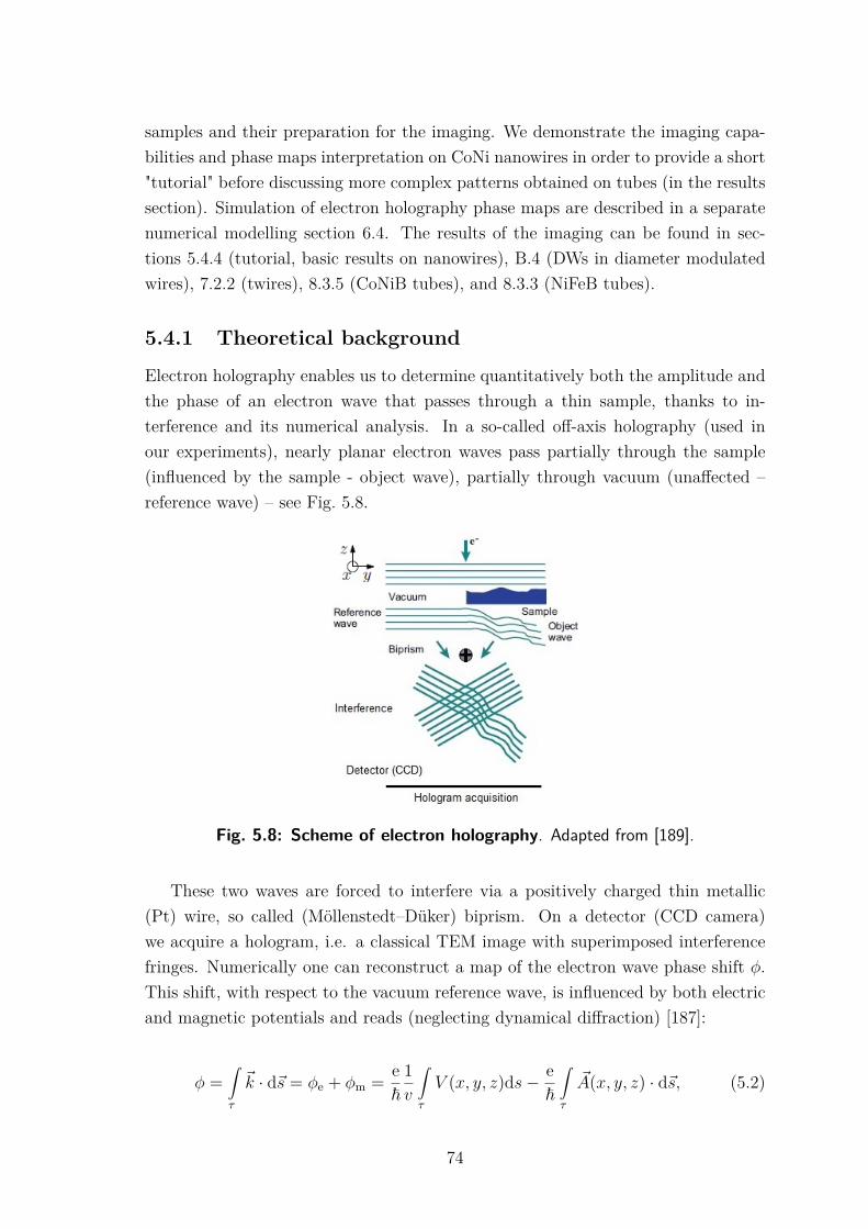
samples and their preparation for the imaging. We demonstrate the imaging capa-bilities and phase maps interpretation on CoNi nanowires in order to provide a short"tutorial" before discussing more complex patterns obtained on tubes (in the resultssection). Simulation of electron holography phase maps are described in a separatenumerical modelling section 6.4. The results of the imaging can be found in sec-tions 5.4.4 (tutorial, basic results on nanowires), B.4 (DWs in diameter modulatedwires), 7.2.2 (twires), 8.3.5 (CoNiB tubes), and 8.3.3 (NiFeB tubes).
5.4.1 Theoretical background
Electron holography enables us to determine quantitatively both the amplitude andthe phase of an electron wave that passes through a thin sample, thanks to in-terference and its numerical analysis. In a so-called off-axis holography (used inour experiments), nearly planar electron waves pass partially through the sample(influenced by the sample - object wave), partially through vacuum (unaffected –reference wave) – see Fig. 5.8.
Fig. 5.8: Scheme of electron holography. Adapted from [189].
These two waves are forced to interfere via a positively charged thin metallic(Pt) wire, so called (Möllenstedt–Düker) biprism. On a detector (CCD camera)we acquire a hologram, i.e. a classical TEM image with superimposed interferencefringes. Numerically one can reconstruct a map of the electron wave phase shift 𝜑.This shift, with respect to the vacuum reference wave, is influenced by both electricand magnetic potentials and reads (neglecting dynamical diffraction) [187]:
𝜑 =∫𝜏
�� · d�� = 𝜑e + 𝜑m = e~
1𝑣
∫𝜏
𝑉 (𝑥, 𝑦, 𝑧)d𝑠 − e~
∫𝜏
��(𝑥, 𝑦, 𝑧) · d��, (5.2)
74
where �� is the relativistic electron wave vector determined for example from theKlein-Gordon-Flock equation or the more general Dirac equation (relativistic ver-sions of the Schrödinger equation for spin equal to 0 and 1/2, respectively), e isthe elementary charge, ~ the reduced Planck constant, 𝑣 the relativistic electronvelocity, 𝑉 (𝑥, 𝑦, 𝑧) stands for electrostatic potential and �� represents the magneticvector potential (magnetic induction �� = ∇ × ��). The integration is taken alongthe electron path represented by a curve 𝜏 . Note, that even for a region withzero magnetic/electric field there is some effect on the electron (charged particle ingeneral), provided that the associated potentials are non-zero – recall the Ehren-berg–Siday–Aharonov–Bohm effect.
For a given accelerating voltage in the transmission electron microscope (e.g.300 kV), terms in front of the first integral on the right hand side of (5.2) are constantand usually grouped together in a parameter labelled c𝐸 (see also appendix B.1;interaction constant 𝜎 in Lichte’s review [187]).
As the electron beam is usually supposed to travel along 𝑧 direction, we canrewrite (5.2) assuming homogeneous sample composition and no external charges,nor fields:
𝜑(𝑥, 𝑦) = c𝐸𝑡(𝑥, 𝑦)𝑉0 − e~
∫𝜏
𝐴𝑧(𝑥, 𝑦, 𝑧)dz, (5.3)
with• c𝐸 = e
~1𝑣, interaction constant depending on electron energy through 𝑣 = 𝑣(𝐸),
c300 keV = 6.5262 · 106 rad/(V · m),• 𝑡(𝑥, 𝑦) – sample thickness (in general electron path length through the sample),• 𝑉0 – electrostatic Mean Inner Potential (MIP, volume averaged electrostatic
potential),• 𝐴𝑧 – 𝑧 (along the beam)-component of magnetic vector potential – depends
only on in-plane magnetic induction 𝐵𝑥, 𝐵𝑦 (components perpendicular to thebeam direction).
The integral in (5.3) is taken from −∞ to +∞, but in practise one takes just thesample surrounding. In a simple case, the electrostatic contribution 𝜑e to the phaseshift is given by the sample thickness and (mostly constant) MIP. In general, theMIP can vary within the sample (used for visualization of different doping levels insemiconductors by electron holography), but for metals of uniform composition itcan be well-approximated by a constant. The values of the MIP were calculated withvarious models for many elements, see e.g. [190]. The values can also be measured,even with the electron holography itself provided that we know other parameters(e.g. sample thickness). This is rather easy for non-magnetic elements with welldefined sample shape and slightly more challenging for magnetic metals. Example
75
of such measurements are covered in a thesis by Signoretti [191], where MIP valueswere determined for electrodeposited cylindrical nanowires, composed of Co, Cu,Ag, and Ni respectively. These values for metals are usually around 20 V (both fromexperiments and various calculations).
The magnetic part of the phase shift can give information about the magneticflux. The difference between 𝜑m at two arbitrary points [𝑥1,𝑦1] and [𝑥2,𝑦2] in a phaseimage,
Δ𝜑m = 𝜑m(𝑥1, 𝑦1) − 𝜑m(𝑥2, 𝑦2) = − e~
∫𝜏
(𝐴𝑧(𝑥1, 𝑦1, 𝑧) − 𝐴𝑧(𝑥2, 𝑦2, 𝑧)) dz, (5.4)
can be rewritten in the form of a loop integral along a rectangular loop Ψ givenby 2 parallel electron trajectories going through the two points and joint at infinityby lines perpendicular to the trajectories [188]. Using Stokes’ theorem, we finallyarrive at the expression with the magnetic flux Φm encompassed by the loop Ψ andcontaining the induction �� =
(∇ × ��
):
Δ𝜑m = − e~
∮Ψ=𝜕Σ
�� · d𝑙 = − e~
x
Σ
(∇ × ��
)· d�� = − e
~
x
Σ
�� · d�� = − e~
Φm, (5.5)
Where �� is a normal to the surface Σ encompassed by the loop Ψ, thereforenormal to the electron (beam) direction. Therefore only in-plane (perpendicularto the electron beam) magnetic induction components contribute to the magneticphase shift. This implies that the sample needs to be tilted to get informationabout the remaining induction component. For a thin film of thickness 𝑡 with arectangular cross-section, normal electron beam incidence and homogeneous in-planemagnetization (and thus induction), the magnetic shift equals Δ𝜑m(𝑥) = −e/~𝐵𝑡𝑥,with 𝑥 being coordinate in-plane of the film.
Phase maps acquired with the tilted sample might be needed for proper assign-ment of the magnetic configuration – different magnetization patterns can give rise tosimilar phase maps. It is possible to remove the electrostatic contribution and thusobtain pure magnetic information by subtracting images acquired with opposite sam-ple magnetization (magnetization reversal), flipping the sample upside-down [192],taking holograms at different acceleration voltage, etc. [193]. More information onelectron holography can be found in reviews [187–189].
5.4.2 Instrumentation & data processing
Concerning the instrumentation, a transmission electron microscope with a highlycoherent electron source is required (cold cathode, FEG=Field Emission Gun) in
76
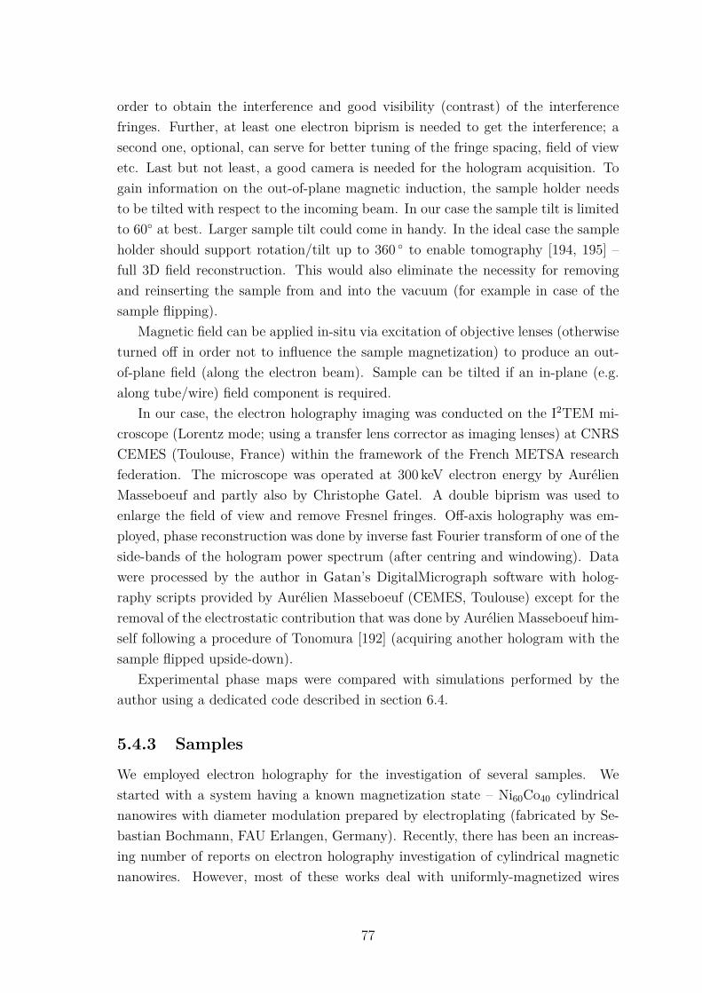
order to obtain the interference and good visibility (contrast) of the interferencefringes. Further, at least one electron biprism is needed to get the interference; asecond one, optional, can serve for better tuning of the fringe spacing, field of viewetc. Last but not least, a good camera is needed for the hologram acquisition. Togain information on the out-of-plane magnetic induction, the sample holder needsto be tilted with respect to the incoming beam. In our case the sample tilt is limitedto 60∘ at best. Larger sample tilt could come in handy. In the ideal case the sampleholder should support rotation/tilt up to 360 ∘ to enable tomography [194, 195] –full 3D field reconstruction. This would also eliminate the necessity for removingand reinserting the sample from and into the vacuum (for example in case of thesample flipping).
Magnetic field can be applied in-situ via excitation of objective lenses (otherwiseturned off in order not to influence the sample magnetization) to produce an out-of-plane field (along the electron beam). Sample can be tilted if an in-plane (e.g.along tube/wire) field component is required.
In our case, the electron holography imaging was conducted on the I2TEM mi-croscope (Lorentz mode; using a transfer lens corrector as imaging lenses) at CNRSCEMES (Toulouse, France) within the framework of the French METSA researchfederation. The microscope was operated at 300 keV electron energy by AurélienMasseboeuf and partly also by Christophe Gatel. A double biprism was used toenlarge the field of view and remove Fresnel fringes. Off-axis holography was em-ployed, phase reconstruction was done by inverse fast Fourier transform of one of theside-bands of the hologram power spectrum (after centring and windowing). Datawere processed by the author in Gatan’s DigitalMicrograph software with holog-raphy scripts provided by Aurélien Masseboeuf (CEMES, Toulouse) except for theremoval of the electrostatic contribution that was done by Aurélien Masseboeuf him-self following a procedure of Tonomura [192] (acquiring another hologram with thesample flipped upside-down).
Experimental phase maps were compared with simulations performed by theauthor using a dedicated code described in section 6.4.
5.4.3 Samples
We employed electron holography for the investigation of several samples. Westarted with a system having a known magnetization state – Ni60Co40 cylindricalnanowires with diameter modulation prepared by electroplating (fabricated by Se-bastian Bochmann, FAU Erlangen, Germany). Recently, there has been an increas-ing number of reports on electron holography investigation of cylindrical magneticnanowires. However, most of these works deal with uniformly-magnetized wires
77

or alternating magnetic and non-magnetic segments (e.g. Co/Cu) – this has beenalready done in 1996 by Beeli et al. [196]. Biziere et al. [14] observed transverse do-main walls in NWs and provided support of numerical simulations of the magneticphase maps. Further, some DWs have been reported in the study by Ivanov andcoworkers [26]. In our work, we could not only prepare and identify a DW, but alsodisplace it with a magnetic field (section B.4).
Later, we moved to more challenging samples: our own electroplated Ni tube-wire nanostructures with smaller diameter (around 60 nm). We also investigatedmagnetic (nano)tubes from CoNiB and NiFeB prepared by electroless plating at TUDarmstadt (by Sandra Schaefer). To the best of our knowledge the only observationof ferromagnetic nanotubes by electron holography has been performed in the groupof Dunin-Borkowski [109] using small aspect ratio (5) CoFeB nanotubes: diameter(hexagonal cross-section) around 200 nm and length of 1 µm. They found axialmagnetization with opposite curling sense at the ends of the tube. In our work, welook at higher aspect ratio tubes (50-100) from different materials.
As substrates we used Cu TEM grids (window size 50 µm) with lacey carbonfilm. Such carbon films have many holes, which increases the chance that at leastpart of the wire/tube is suspended in vacuum (no substrate contribution) duringthe observation. This facilitates the electrostatic part removal. Nanostructureswere transferred on the grid from a suspension (nanostructures in isopropyl alco-hol). For NiCo nanowires we used the grid as a filter and forced the liquid toflow through with a syringe. In this way, large amounts of nanostructures couldbe collected, if the syringe piston was moved slowly (otherwise the film could bedamaged and windows in the grid are empty). When we tried to repeat the proce-dure for the electroless-deposited tubes, we obtained many damaged tubes (broken,unrolled, . . . ). Therefore, in case of tubes we used a micropipette to transfer severaldroplets of the solution with tubes on the grid. The solvent was left to evaporate.This resulted in a much lower density of structures (it could be increased for higherdensity of structures in the solution/solvent), but they retained the tubular shapeand the sample was slightly cleaner.
An optical microscopy image of the grid and example of structures dispersed onthe porous C film are given in Fig. 5.9. Prior to the electron holography investiga-tion, in some cases, suitable structures (isolated, parts suspended, low amount ofstructural defects) were identified based on optical and scanning electron microscopyimaging. Just with the optical microscope one can locate nanowires (diameter ofthe thin section around 120 nm), but one cannot tell for sure whether it is a singlewire or a bundle (couple, triplet) as they are well below the resolution of the opticalmicroscope.
78
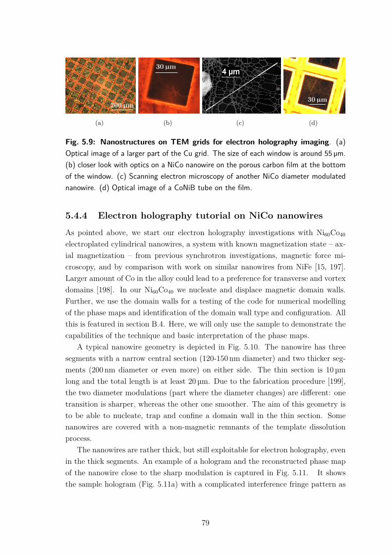
200µm
(a)
30µm
(b) (c)
30µm
(d)
Fig. 5.9: Nanostructures on TEM grids for electron holography imaging. (a)Optical image of a larger part of the Cu grid. The size of each window is around 55 µm.(b) closer look with optics on a NiCo nanowire on the porous carbon film at the bottomof the window. (c) Scanning electron microscopy of another NiCo diameter modulatednanowire. (d) Optical image of a CoNiB tube on the film.
5.4.4 Electron holography tutorial on NiCo nanowires
As pointed above, we start our electron holography investigations with Ni60Co40
electroplated cylindrical nanowires, a system with known magnetization state – ax-ial magnetization – from previous synchrotron investigations, magnetic force mi-croscopy, and by comparison with work on similar nanowires from NiFe [15, 197].Larger amount of Co in the alloy could lead to a preference for transverse and vortexdomains [198]. In our Ni60Co40 we nucleate and displace magnetic domain walls.Further, we use the domain walls for a testing of the code for numerical modellingof the phase maps and identification of the domain wall type and configuration. Allthis is featured in section B.4. Here, we will only use the sample to demonstrate thecapabilities of the technique and basic interpretation of the phase maps.
A typical nanowire geometry is depicted in Fig. 5.10. The nanowire has threesegments with a narrow central section (120-150 nm diameter) and two thicker seg-ments (200 nm diameter or even more) on either side. The thin section is 10 µmlong and the total length is at least 20 µm. Due to the fabrication procedure [199],the two diameter modulations (part where the diameter changes) are different: onetransition is sharper, whereas the other one smoother. The aim of this geometry isto be able to nucleate, trap and confine a domain wall in the thin section. Somenanowires are covered with a non-magnetic remnants of the template dissolutionprocess.
The nanowires are rather thick, but still exploitable for electron holography, evenin the thick segments. An example of a hologram and the reconstructed phase mapof the nanowire close to the sharp modulation is captured in Fig. 5.11. It showsthe sample hologram (Fig. 5.11a) with a complicated interference fringe pattern as
79

Fig. 5.10: Example of the NiCo diameter-modulated nanowire on a Si sub-strate. The central, thin section has diameter around 150 nm and length 10 µm. Thispart is positioned in between two thicker segments (200 nm in diameter or even more).Note the non-magnetic impurities on the right side of the wire originating from thetemplate dissolution process.
Car
bon
film
(a) sample hologram (b) reference hologram
~M Stra
yfie
ld
Stra
yfie
ld
(c) wrapped phase
~M
(image processing)Artefact
(d) unwrapped phase (continuous)
Fig. 5.11: Electron holography of a NiCo nanowire – from hologram to phasemap. (a) Nanowire and (b) reference (without sample) holograms with insets showinga closer look on the fringes. (c) Reconstructed phase maps: (c) wrapped phase (in[0,2𝜋] interval) with contour lines following the magnetic induction direction and (d)continuous (unwrapped) phase with the inset showing a line profile across the wire.
80
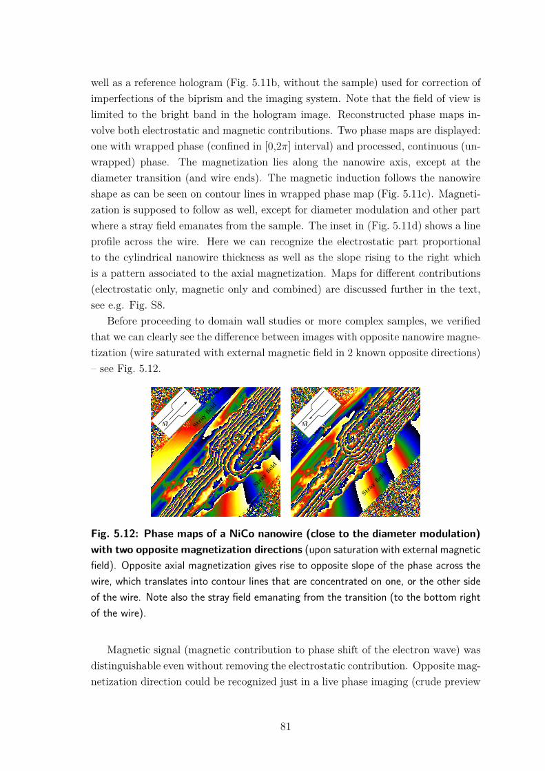
well as a reference hologram (Fig. 5.11b, without the sample) used for correction ofimperfections of the biprism and the imaging system. Note that the field of view islimited to the bright band in the hologram image. Reconstructed phase maps in-volve both electrostatic and magnetic contributions. Two phase maps are displayed:one with wrapped phase (confined in [0,2𝜋] interval) and processed, continuous (un-wrapped) phase. The magnetization lies along the nanowire axis, except at thediameter transition (and wire ends). The magnetic induction follows the nanowireshape as can be seen on contour lines in wrapped phase map (Fig. 5.11c). Magneti-zation is supposed to follow as well, except for diameter modulation and other partwhere a stray field emanates from the sample. The inset in (Fig. 5.11d) shows a lineprofile across the wire. Here we can recognize the electrostatic part proportionalto the cylindrical nanowire thickness as well as the slope rising to the right whichis a pattern associated to the axial magnetization. Maps for different contributions(electrostatic only, magnetic only and combined) are discussed further in the text,see e.g. Fig. S8.
Before proceeding to domain wall studies or more complex samples, we verifiedthat we can clearly see the difference between images with opposite nanowire magne-tization (wire saturated with external magnetic field in 2 known opposite directions)– see Fig. 5.12.
~M Stra
yfie
ld
Stra
yfie
ld
~M
Stra
yfie
ld
Fig. 5.12: Phase maps of a NiCo nanowire (close to the diameter modulation)with two opposite magnetization directions (upon saturation with external magneticfield). Opposite axial magnetization gives rise to opposite slope of the phase across thewire, which translates into contour lines that are concentrated on one, or the other sideof the wire. Note also the stray field emanating from the transition (to the bottom rightof the wire).
Magnetic signal (magnetic contribution to phase shift of the electron wave) wasdistinguishable even without removing the electrostatic contribution. Opposite mag-netization direction could be recognized just in a live phase imaging (crude preview
81
obtained within several seconds) thanks to a different phase gradient across thewire detonated by contour lines (concentrated at opposite sides of the wire). Thisis crucial for fast identification of a domain wall presence and its position. Notethat the magnetization is non-uniform in the diameter modulation, this gives rise tomagnetic charges and a stray field emanating from this nanowire section (Fig. 5.12).The stray field is also manifested on the phase maps outside the wire near the mod-ulation. This is more visible to the bottom right in Fig. 5.12. There is a carbon film(part of the substrate) on the other side of the wire (visible in Fig. 5.11a), whichpartially conceals the stray field lines.
More elaborated imaging with domain walls in nanowires and comparison withnumerical modelling is described in section B.4, investigation of twires in 7.2.2, andfinally study of tubes is covered in sections 8.3.5 (CoNiB tubes) and 8.3.3 (NiFeBtubes).
5.5 Magnetometry
We measured hysteresis loops of magnetic NTs both for their arrays (global magne-tometry) and also single tubes (local magneto-optics with focused laser beam).
5.5.1 VSM-SQUID
For global magnetometry, measurement of arrays of (nano)tubes still in a template,we used a Quantum design MPMS SQUID VSM (Magnetic Property MeasurementSystem - Superconducting Quantum Interference Device - Vibrating Sample Mag-netometer). Samples were placed on a quartz or straw holder. After introductioninto the measurement chamber and before acquisition of hysteresis loops, the samplewas AC demagnetized along the applied field direction.
A cleaned empty holder was measured first (for each new sample to verify theholder cleanliness), its contribution was insignificant. Therefore, it was not necessaryto remove such contribution. Further, we also considered a possible contribution ofthe template: both alumina and polycarbonate provided only weak diamagneticcontribution, which was disregarded as well in further studies.
5.5.2 Magneto-optics with focused laser beam
Single tubes dispersed on a Si substrate were probed by the Magneto-Optical KerrEffect (MOKE) that relies on a change of polarization plane and ellipticity of apolarized light upon a reflection from a magnetic sample. The technique is rathersurface sensitive, providing information from the depth up to approximately 30 nm
82
(depending on material, wavelength, etc.). The MOKE was implemented in the lon-gitudinal configuration with a focused He-Ne (𝜆 = 632.8 nm) laser (100x objective,laser spot 1 µm). The field was swept as a triangular wave signal, with frequency1.1 Hz, and field calibration uncertainty max ±5 mT. In order to limit the poten-tial effect of heating, the laser power was set to 0.2 mW. Commonly even few mWlaser power is used for the investigation of magnetic nanostructures. In our mea-surements, such laser power leads to more squared loops (heat assisted switching)and prolongated exposure can damage our samples – see appendix A.2. The samplewith tubes is placed on a piezostage, therefore the focused beam can be preciselypositioned on a particular tube. Further information on the field of magneto-opticscan be found in a book by Štefan Višňovský [200].
83
6 SIMULATIONS
To support our experimental observations and also to get better insight into themagnetic systems under investigation, we run numerical micromagnetic simulationsof magnetization distribution in our samples – nanotubes and nanowires. Further, weemployed modelling of the contrast expected for employed experimental techniques– namely electron holography and synchrotron based experiments with circularlypolarized X-rays (XMCD-PEEM, STXM).
6.1 Micromagnetics
We used the following micromagnetic codes:• Object Oriented MicroMagnetic Framework (OOMMF) [201]• Finite Element LLG Object Oriented Development (FeeLLGood) [202, 203]All micromagnetic simulations were performed at 0 K. Most simulations are done
on permalloy or permalloy-like structures (for both nanowires and nanonotubes),therefore considering only exchange, magnetostatic and possibly Zeeman energy. Asfor simulation parameters we thus use exchange stiffness 𝐴 = 13·10−12 J/m and spon-taneous magnetization 𝜇0𝑀s = 1 T if not stated otherwise. For the tubes with az-imuthal (flux-closure) magnetization we also added an effective uniaxial anisotropy.We considered two ways for obtaining the azimuthal magnetization:
• point-wise varying easy axis that follow the azimuthal direction in every cell(implemented in OOMMF)
• constant hard axis along the tube axis (easily used in any code, exploited inFeeLLGood and thus presented in most cases shown here)
Below we provide additional information related to the used micromagneticcodes.
6.2 Object Oriented MicroMagnetic Framework
OOMMF is a public micromagnetic solver from NIST [201]. This finite differencecode (discretization in parallelepipeds, commonly cubes) can solve the problem ei-ther by a numerical integration of the LLG equation or by minimizing the energyfunctional.
We used OOMMF (version 1.2a4; 1.2a6 for tubes with larger diameters) mainlyfor the first tests at the beginning of each set of new simulations (NTs, NTs withazimuthal anisotropy, multilayered tubes) where we profited from the code versatil-ity. Later we used FeeLLGood for the better description of curved geometries and
84
also in order to benefit for its post-processing tools for modelling of experimentalmeasurement techniques (more below).
Visualization of micromagnetic configurations was done mainly using nativemmdisp tool. In some cases, the tool ovf2vtk [204] was employed for conversion ofOOMMF format (OVF) to Visualisation ToolKit (VTK) file format for the visual-ization in ParaView software [205]. In these cases a threshold filter on magnetizationvector magnitude had to be imposed in ParaView in order to remove zero-lengthvector artefacts (zero-length vectors oriented in one direction displayed on top ofthe real magnetic configuration).
6.3 FeeLLGood
FeeLLGood [202, 203] is a finite element code developed at Institut Néel by Jean-Christophe Toussaint. Further information on the code and its development canbe found in PhD theses of Adrien Vaysset [206] and Ségolène Jamet [207]. For oursimulations we employed version STDW 20150821 (using ScalFMM library [208] incomputation of magnetostatic interactions). As we are dealing with finite elements,the geometry creation and meshing is not as straightforward as in finite differences.We address these points below, mainly utilizing Gmsh (free finite element meshgenerator and geometry editor) [209]. Visualization of the resulting micromagneticconfigurations as well as outcomes of the post-processing codes was done in Par-aView [205].
6.3.1 Geometry and meshing
Simple geometries (wire, tube) were prepared directly in Gmsh using built-in scriptsfor extrusion of a disk or an annulus to prepare nanowires or nanotubes, respectively.When we tried to create a more complex system, such as coaxial (multi-layered)tubes, in Gmsh by extrusion of two 2D concentric annuli, the resulting geometry(combination of structured and unstructured grid) could not be meshed properly.We tried different meshing methods (Frontal, Delaunay) and various mesh post-processing (smoothing steps, mesh optimization), but without success (Gmsh pro-gram even got frozen or completely crashed for some combinations, others causedproblems in the micromagnetic code itself).
In order to overcome this obstacle, we created the geometry in an externalComputer-Aided Design (CAD) software. We used FreeCAD [210], but in prin-ciple any CAD can be used provided that the geometry can be exported to formatthat can be read by Gmsh. We successfully performed this step by exporting tobrep (boundary representation) format (stp or iges should work as well). One then
85
only needs to define physical volume(s) and surfaces. For more complex geometriesit is more convenient to use external CAD with much more user friendly interfacethan Gmsh one. On the other hand, even slight changes of geometry (i.e. differentdiameters, length, . . . ) require repeated exporting/importing of the geometry aswell as specifying maximum element size (tetrahedron edge).
Even a mesh prepared using a CAD geometry caused some errors in the micro-magnetic simulations. Finally, this problem was solved by performing more meshpost-processing which should improve the mesh quality. Experimentally we foundthat meshing in Gmsh with 3 smoothing steps and 1 Lloyd smoothing step followedby a common Optimize 3D (Netgen) works well. Other post-processing may do thejob as well, but here we will stick to the one mentioned above.
In case of simple wire or tube geometry, we employed the Delaunay 3D meshingmethod and used only Optimize 3D (Netgen) procedure (no smoothing).
In all cases, the mesh represented by a sparse matrix is subject to Cuthill–McKee(CMK) ordering algorithm to decrease the bandwidth of the band matrix (scriptimplemented by Jean-Christophe Toussaint) to ease and speed up the numericalcomputation.
Note on element size - mesh smoothing
Mesh smoothing not only improves the mesh, but may also result in a slight changein the size of some elements (changes in positions of nodes). It seems that themaximum element size is slightly increased upon the smoothing. In an examplebelow (tube wall thickness of 15 nm), the maximum element size is slightly biggerthan the desired value of 4 nm but still well below 4.5 nm. This difference wasremarkable when we compared a tube prepared using just Gmsh and two coaxialtubes created in the FreeCAD and smoothing the mesh as described above. Thenon-smoothed tube had more nodes than both coaxial tubes together as can be seenin Fig. 6.1. Gmsh script with Lc=4 nm without the smoothing generates smallerelements, sometimes maybe even unnecessarily small.
6.3.2 Initial magnetic configuration
As an initial magnetic configuration one may use either the state from previoussimulations or utilize a c++ script that assigns a unit magnetization vector to eachnode of the mesh based on a given analytical expression. In order to define differentmagnetization regions (e.g. two opposite domains and a DW), simple (nested) ifconditions are applied. An example is given in the annex section C.
86
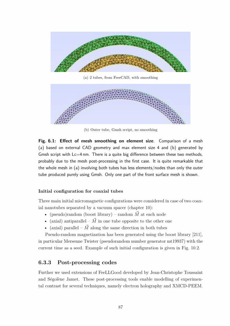
(a) 2 tubes, from FreeCAD, with smoothing
(b) Outer tube, Gmsh script, no smoothing
Fig. 6.1: Effect of mesh smoothing on element size. Comparison of a mesh(a) based on external CAD geometry and max element size 4 and (b) generated byGmsh script with Lc=4 nm. There is a quite big difference between these two methods,probably due to the mesh post-processing in the first case. It is quite remarkable thatthe whole mesh in (a) involving both tubes has less elements/nodes than only the outertube produced purely using Gmsh. Only one part of the front surface mesh is shown.
Initial configuration for coaxial tubes
Three main initial micromagnetic configurations were considered in case of two coax-ial nanotubes separated by a vacuum spacer (chapter 10):
• (pseudo)random (boost library) – random �� at each node• (axial) antiparallel – �� in one tube opposite to the other one• (axial) parallel – �� along the same direction in both tubesPseudo-random magnetization has been generated using the boost library [211],
in particular Mersenne Twister (pseudorandom number generator mt19937) with thecurrent time as a seed. Example of such initial configuration is given in Fig. 10.2.
6.3.3 Post-processing codes
Further we used extensions of FeeLLGood developed by Jean-Christophe Toussaintand Ségolène Jamet. These post-processing tools enable modelling of experimen-tal contrast for several techniques, namely electron holography and XMCD-PEEM.
87

These are detailed in sections below.
6.4 Electron-holography code
Electron holography phase maps are not always easy to interpret. In order to facil-itate this task we performed a numerical modelling of the phase shift maps. Firstwe compute a relaxed 3D micromagnetic configuration using the FeeLLGood code(finite elements). In this way, we prepare one or several possible micromagneticconfigurations we expect to appear in our system. The relaxed micromagnetic con-figuration is then used as an input for the calculation of the electron holographyphase maps. Our technique combines both computational efficiency and precisionwhich is uncommon for a numerical method, mainly due to the transformation of a3D problem to a 2D one. Instead of performing the calculation in the whole (𝑥,𝑦,𝑧)space like in [14], the magnetic phase shift is proportional to the 𝑧-component ofthe magnetic vector potential produced by a 2D equivalent magnetic system whosein-plane magnetization components are given by the path integral
∫𝜏
(𝑀𝑦, −𝑀𝑥) d𝑧,where 𝑧 denotes the beam direction. The latter expression corresponds to the inte-grated (along the electron path) in-plane magnetization of the 3D original systemrotated by 90 ∘ around the beam axis. This can be done for different sample tilt-s/rotations and both magnetic and electrostatic contributions to the electron phaseshift.
For the 2D projection we use a frontal meshing method, the mesh has order 2 andit is optimized in a similar way to the 3D mesh used in micromagnetic simulations.The maximum cell size is 8 nm (but order 2, so effectively 4 nm), finer mesh of 4-5 nmwas used for more refined modelling. But no significant difference has been foundfor the samples we model.
In experiments it is not always easy to obtain pure magnetic contrast. Thereforethe idea is to include the electrostatic contribution in the numeric simulations. Insuch a case, we assume the electrostatic contribution to be proportional to thesample thickness and to the volume-averaged Mean Inner Potential of 22 V with theconstant of proportionality c300 keV = 6.5262 · 106 rad/(V · m) [187].
Unfortunately, in the current version of the code (v. 20151117), the electrostaticcontribution can be modelled properly only for solid objects. In case of a tube thecode assumes the thickness to be equal to the outer diameter and it disregards theinner hollow part. However, it is possible to take the hollow part into account: onecan just subtract simulation of the electrostatic phase (setting 𝑀s = 0) calculatedfor a solid wire corresponding geometrically to the inner hollow part of the tube (seeFig. S4). In order to avoid artefacts, the same 2D mesh is used for the projection
88

of both tube and the "inner wire".
6.4.1 NiCo nanowires
As for the micromagnetic simulation of the nanowires only exchange and dipolarinteractions were taken into account (thus neglecting magnetocrystalline anisotropy)with the following parameters: saturation polarization 𝜇0Ms = 1 T and exchangestiffness 𝐴 = 10−11 J/m. The wire diameter is 120 nm, same as in the experiment(central thin section of the wires). The tetrahedron size was 5 nm or smaller. Weconsider a wire with the length sufficiently longer than the DW width, however muchshorter than in the experiment. Magnetic charges are removed at either end, thusmimicking an infinitely long wire. In wire we considered two axial domains with aDW (either TW, or BPW). The computation was done for different wire tilts anddomain wall orientation (azimuth for the TW) for both magnetic and electrostaticcontribution.
6.4.2 Tubes
In the case of tubes, we focussed on azimuthal domains separated by the Néel,Bloch or cross-tie walls, that were obtained by previous relaxation of micromagneticconfigurations. For the relaxation we started with axial magnetization in the DWfor the Néel wall and with radial magnetization for the other two. The cross-tieis obtained for thinner tube shells and smaller effective anisotropy constants. Weconsidered permalloy-like material with uniaxial anisotropy having hard axis alongthe tube axis to promote the azimuthal domains.
Note that the simulations presented here are crude. They are based on a smalltube for the Bloch wall – diameter 50 nm, tube wall thickness of 10 nm; Néel andcross-tie walls (4 pairs of vortices and antivortices) were modelled in a larger tubewith diameter 250 nm and 20 nm tube wall thickness. The micromagnetic configu-ration is prepared in FeeLLGood with mesh size 4 nm or smaller. For the electronholography projection, the 2D mesh element size was 6 or even 8 nm (for the cross-tie in the larger tube), a smaller size can be used for more refined results. Still theabove-mentioned mesh size should be fine as it is a 2nd order mesh; test with smallermesh did not reveal any significant difference.
6.5 XMCD-PEEM code
The implementation of the shadow-XMCD contrast modelling (including X-ray ab-sorption, photoelectron emission, and their detection) is detailed in the work of
89

Jamet et al. [153, 207]. As an input magnetic configuration one can use either ananalytical expression for the magnetization distribution, or a relaxed micromagneticconfiguration (computed with the above-mentioned FeeLLGood code).
For comparison with experiments on CoNiB tubes (imaging performed at Co-L3
edge), we assume the X-ray linear absorption coefficients 𝜇 to be those for pure cobaltmultiplied by the atomic fraction of cobalt in the tube material. We disregard theboron influence and also suppose that Ni absorption at the Co-L3 edge is negligibleas we are well below the Ni-L absorption edges. Namely we used 𝜇+ = 0.038 nm−1
and 𝜇− = 0.064 nm−1 for two opposite circular polarizations of the X-ray beam (datafor pure elements extracted from Nakajima’s work[212]).
Some tests and qualitative comparisons were made also for permalloy(-like)nanostructures (Ni80Fe20). In these cases, we consider XMCD at Fe-L3 and the X-raylinear absorption coefficients are 𝜇+ = 0.010 nm−1 and 𝜇− = 0.018 nm−1 [153], i.e.we again neglect Ni absorption (we are below Ni L edges) and take proportion of Feinto account. Basically, a larger difference between the coefficients is equivalent toa larger thickness of the magnetic material (e.g. tube wall thickness). As we do notaim to do quantitative, but only qualitative comparison with the experiments, theexact values are not of high importance. Further, quantitative comparison is any-how challenging due to fine experimental features such as background level contrastaffecting relative intensity from the surface with respect to the shadow. Neverthe-less, one should note that larger material thickness or 𝜇 may lead to some changes:namely different proportion of the XMCD intensity coming from the nanostruc-ture surface and from the shadow, as well as inversion of contrast at the edge of ananostructure surface [153].
90

Part III
Results & DiscussionMagnetic nanotubes
91
7 SYNTHESIS OF NANOTUBES
Below we will describe the results of our attempts for synthesis of magnetic nan-otubes. Tubes prepared at TU Darmstadt [127] will not be covered in this section.We used two electrochemical methods to prepare the tubes: electroplating whereelectrons for reduction of metallic ions (from an aqueous solution) are supplied byan external current source, and electroless plating where electrons are provided ina reaction with the so-called reducing agent. More information on the depositionprocess can be found in the methods, chapter 4.
7.1 Electroplating of NiCo nanotubes
Using electroplating we prepared nanotubes from NiCo and Ni, as well as Ni nanos-tructures with alternating wire and tube segments. These were obtained by em-ploying a thin porous working electrode (see methods, section 4.2). We also triedto fabricate Ni/Cu core-shell nanowires [129] and Ni nanotubes by electrochemicaletching of the Cu core, and pulsed electrodeposition of Ni [164]. However, in ourcase such nanotube preparations turned out to be highly unreliable and yielded atbest very poor tubular-like structures with high roughness. Therefore we will focusbelow on the two afore-mentioned nanotube fabrication procedures (electrodeposi-tion of NiCo and Ni with porous working electrode). In this section we will dealonly with NiCo nanostructures, Ni tubes and wire-tube elements are described insection 7.2.
Following the article by Zhang [166] we electroplated NiCo inside nanoporousalumina membranes starting from the porous Au electrode at the bottom (porediameter 80-90 nm). Among the fabricated structures, a vast majority consists ofnanotubes with extremely thin walls (few nm) as revealed by transmission electronmicroscopy (Fig. 7.1). Due to prolonged exposition of the magnetic material tosodium hydroxide during the template dissolution, we expect these tubes to bealmost completely oxidized, therefore of no use (if one does not want to studyantiferromagnetic tubes). Aside from these structures we identified a few nanowiresand several tubes with significantly thicker walls (10-20 nm).
Nanowires and nanotubes formed during the deposition had different chemicalcomposition and crystallinity. Nanowires appeared to be Co-rich and well crystal-lized with a preferred texture, some parts almost monocrystalline (Fig. 7.2a). Onthe other hand, the nanotubes were polycrystalline without any preferred crystal-lographic direction (Fig. 7.2b) and they contained almost an equal amount of Niand Co (some tubes were even slightly richer in Ni). We tried to image both NiConanowires and nanotubes with magnetic force microscopy and XMCD-PEEM. For
92

(a) (b)
Fig. 7.1: Transmission electron microscopy of electroplated NiCo nanostruc-tures. (a) The vast majority of structures are nanotubes with a very thin wall (fewnanometers). (b) Direct comparison between hollow nanotubes and a solid nanowireobtained in the same batch. Only a few nanowires were found.
(a) Nanowire (diameter ≈ 100 nm)
(b) Nanotube (diameter ≈ 70 nm, tube wall 10-18 nm)
Fig. 7.2: Different NiCo nanostructures electroplated in the same template: (a)nanowire and (b) nanotube. Transmission electron microscopy images with selective areaelectron diffraction on the right. All observed nanowires were well crystallised with somebeing close to monocrystals. On the other hand, all probed tubes were polycrystalline.
93

NTs we obtained very weak signal only from XMCD-PEEM, however with no clearmagnetic pattern, and nothing with MFM. This is consistent with our expectationthat the NTs are significantly oxidized. On the other hand, for nanowires we ob-tained clear signal with both technique, showing a multidomain structure (Fig 7.3).
(a) MFM
Shadow
WireBeam
(b) XMCD-PEEM at Co-L3 (another wire)
Fig. 7.3: Magnetic domains in Co-rich NiCo nanowires (diameter 100 nm) vi-sualized by magnetic microscopies. (a) MFM and (b) XMCD-PEEM at Co-L3 ofanother nanowire, contrast range 10 %; beam arrives from the top close to perpendicularto the wire – i.e. we see contrast on the wire surface and just behind it inverted contrastin the shadow (separated by the red dashed line). Strong contrast with the transversebeam direction indicates that magnetization has significant transverse component.
In both MFM one can identify two domain types: elongated domains with weakercontrast that sometimes appear to be dipolar (in direction traverse to the wire axis)and smaller domains with slightly stronger contrast that form series with alternat-ing contrast and thus magnetization direction. Both types can be associated totransverse magnetization, just with different orientation: stronger contrast can re-sult from short domains having significant out-of-plane magnetization component,weaker dipolar contrast can arisein case of transverse magnetization lying in-planewith respect to the supporting substrate. The XMCD-PEEM image of another wirefrom the same sample also show similar patterns (elongated domains and smalleralternating ones). As the X-ray beam is nearly perpendicular to the wire axis, themagnetization in the domains is indeed predominantly transverse.
Similar images by MFM has been already acquired by several groups. As forXMCD-PEEM, there is a recent observation of a similar patterns by Bran et al. [198].According to their work, short domains, e.g. seen as checker board pattern inparts of Fig 7.3b should correspond to a transverse magnetization with alternatingdirection (component along and antiparallel to the beam, leading to magnetic flux-closure), whereas the elongated domains rather to vortex ones (but here one wouldexpect almost no contrast in MFM). Note that just from such image alone onecannot clearly tell apart transverse and vortex domain. Without more details onthe supposed vortex showing gradual contrast change in the shadow, it can rathertransverse magnetization in the elongated domain, maybe just wit slightly different
94
orientation. Still such elongated transverse magnetization would be unfavourable,nevertheless possible as a metastable state.
7.2 Ni twires – wire-tube nanoelements
In this section we will describe results of synthesis and briefly also measurementsperformed on tube-wire nanoelements – twires. We have already discussed what hasbeen done on twires in the literature in section 3.6.
7.2.1 Electroplating of Ni wire-tube nanoelements
When we tried to fabricate Ni nanotubes following the electroplating procedure pub-lished by Proenca et al. [123], we obtained mainly nanowires. TEM observationsrevealed also possible remains of destroyed tubes and most importantly several struc-tures with wire and tube segments (Fig. 7.4).
It is striking that for our Ni twires the transition between the nanowire andthe nanotube segment is very sharp. Some structures feature multiple transitionsof this kind (Fig. 7.4c). The tube segments in such twires have length rangingfrom hundreds of nanometres to few microns (longest one observed: 2.2 µm, butthere could be even longer ones). We attribute the presence of these twires tolocal instabilities during the deposition – local change of pH, concentration of thesolution, defect, . . . Following the kinetic model by Philippe and Michler [29] it couldbe possible to achieve an improved control over the deposition process.
7.2.2 Further TEM and electron holography on Ni twire
For the electron holography imaging, we found a rather nice twire, a nanostructurewith a tube segment between two wire parts– consult Fig 7.5(a). From higherresolution TEM images we could see that the tube wall thickness is not completelyuniform, it is below 10 nm, 5-7 nm in most cases. According to selected area electrondiffraction, both tube and wire parts are polycrystalline with some wire parts beingclose to monocrystalline. Damaged tube-like structure to the right of our twire[Fig 7.5(a)] showed no diffraction at all.
Unfortunately, no clear magnetic signal was observed in a quick phase map pre-view even for the nanowire parts, unlike for the NiCo wires mentioned above. Onlyafter removing the electrostatic contribution, we could see that magnetization isaxial and more or less uniform along the wire and there is a stray field emanatingfrom the wire-tube transition as captured in Fig 7.5(c). Unfortunately, small tube
95

(a) Ni nanowires and twires
(b) Broken twire
Wire Tube TubeWire200 nm
(c) Wire-Tube-Wire-Tube
Fig. 7.4: Transmission electron microscopy images of Ni twires (wire-tube na-noelements) after long dissolution of the template (one day). (a) The majority of nanos-tructures is formed by solid nanowires, further there are some nanotubes and small por-tion of tube-wire elements (twires). (b) Broken twire: as the tube wall thickness is verysmall, many tubes and twires are damaged (if not completely destroyed) during process-ing of the solution with nanostructures after the template dissolution. (c) Example of atwire with alternating segments (wire-tube-wire-tube). A small nanowire lies across thefirst tube segment.
96
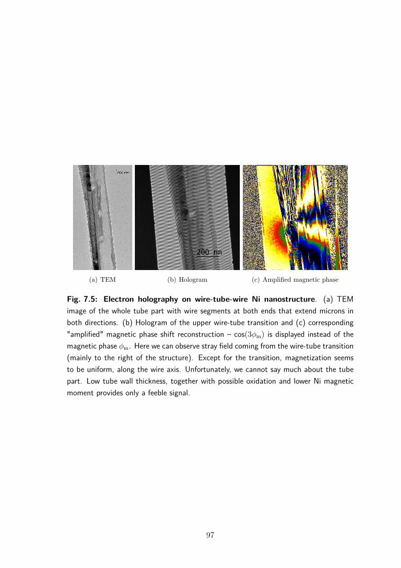
(a) TEM (b) Hologram (c) Amplified magnetic phase
Fig. 7.5: Electron holography on wire-tube-wire Ni nanostructure. (a) TEMimage of the whole tube part with wire segments at both ends that extend microns inboth directions. (b) Hologram of the upper wire-tube transition and (c) corresponding"amplified" magnetic phase shift reconstruction – cos(3𝜑m) is displayed instead of themagnetic phase 𝜑m. Here we can observe stray field coming from the wire-tube transition(mainly to the right of the structure). Except for the transition, magnetization seemsto be uniform, along the wire axis. Unfortunately, we cannot say much about the tubepart. Low tube wall thickness, together with possible oxidation and lower Ni magneticmoment provides only a feeble signal.
97
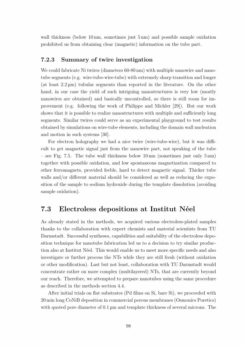
wall thickness (below 10 nm, sometimes just 5 nm) and possible sample oxidationprohibited us from obtaining clear (magnetic) information on the tube part.
7.2.3 Summary of twire investigation
We could fabricate Ni twires (diameters 60-80 nm) with multiple nanowire and nano-tube segments (e.g. wire-tube-wire-tube) with extremely sharp transition and longer(at least 2.2 µm) tubular segments than reported in the literature. On the otherhand, in our case the yield of such intriguing nanostructures is very low (mostlynanowires are obtained) and basically uncontrolled, so there is still room for im-provement (e.g. following the work of Philippe and Michler [29]). But our workshows that it is possible to realize nanostructures with multiple and sufficiently longsegments. Similar twires could serve as an experimental playground to test resultsobtained by simulations on wire-tube elements, including the domain wall nucleationand motion in such systems [30].
For electron holography we had a nice twire (wire-tube-wire), but it was diffi-cult to get magnetic signal just from the nanowire part, not speaking of the tube– see Fig. 7.5. The tube wall thickness below 10 nm (sometimes just only 5 nm)together with possible oxidation, and low spontaneous magnetization compared toother ferromagnets, provided feeble, hard to detect magnetic signal. Thicker tubewalls and/or different material should be considered as well as reducing the expo-sition of the sample to sodium hydroxide during the template dissolution (avoidingsample oxidation).
7.3 Electroless depositions at Institut Néel
As already stated in the methods, we acquired various electroless-plated samplesthanks to the collaboration with expert chemists and material scientists from TUDarmstadt. Successful syntheses, capabilities and suitability of the electroless depo-sition technique for nanotube fabrication led us to a decision to try similar produc-tion also at Institut Néel. This would enable us to meet more specific needs and alsoinvestigate or further process the NTs while they are still fresh (without oxidationor other modification). Last but not least, collaboration with TU Darmstadt wouldconcentrate rather on more complex (multilayered) NTs, that are currently beyondour reach. Therefore, we attempted to prepare nanotubes using the same procedureas described in the methods section 4.4.
After initial trials on flat substrates (Pd films on Si, bare Si), we proceeded with20 min long CoNiB deposition in commercial porous membranes (Osmonics Poretics)with quoted pore diameter of 0.1 µm and template thickness of several microns. The
98
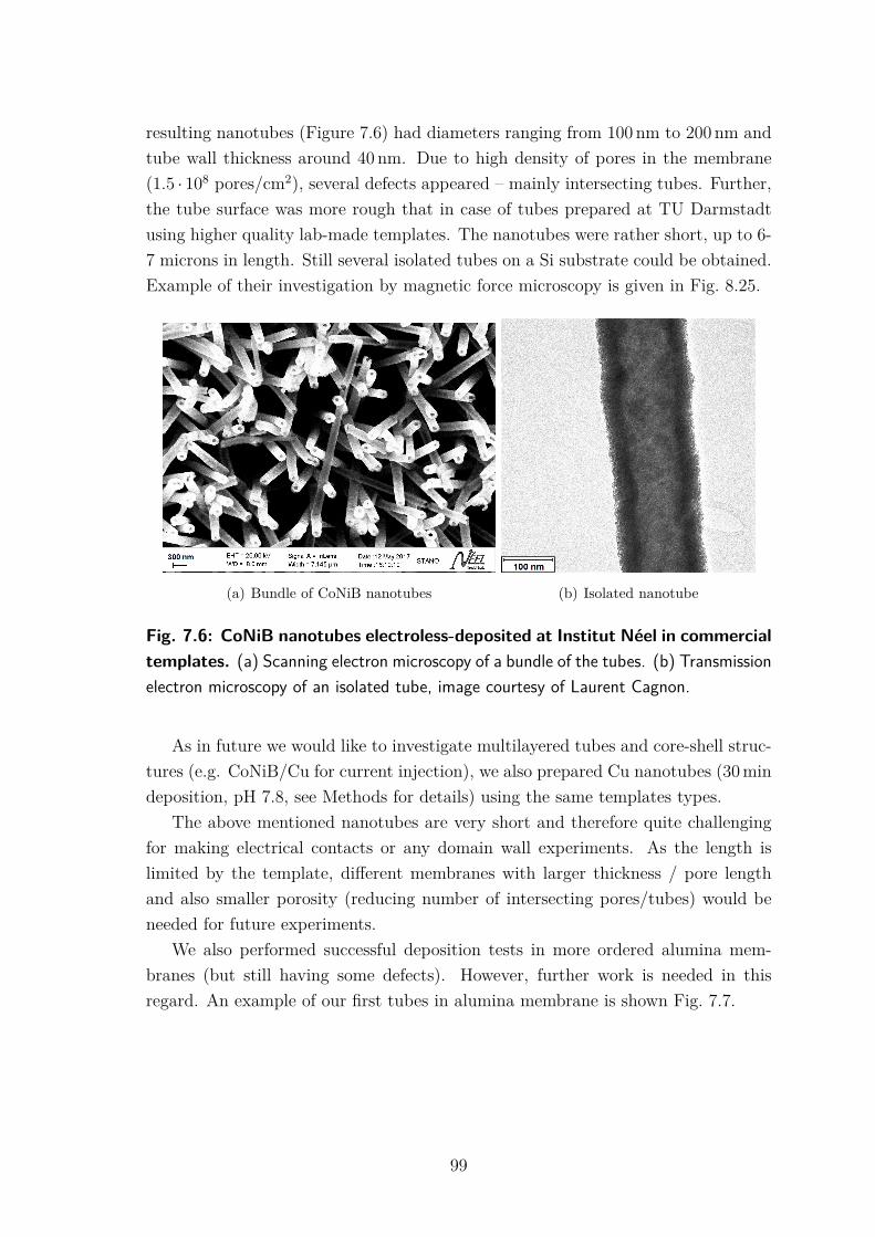
resulting nanotubes (Figure 7.6) had diameters ranging from 100 nm to 200 nm andtube wall thickness around 40 nm. Due to high density of pores in the membrane(1.5 · 108 pores/cm2), several defects appeared – mainly intersecting tubes. Further,the tube surface was more rough that in case of tubes prepared at TU Darmstadtusing higher quality lab-made templates. The nanotubes were rather short, up to 6-7 microns in length. Still several isolated tubes on a Si substrate could be obtained.Example of their investigation by magnetic force microscopy is given in Fig. 8.25.
(a) Bundle of CoNiB nanotubes (b) Isolated nanotube
Fig. 7.6: CoNiB nanotubes electroless-deposited at Institut Néel in commercialtemplates. (a) Scanning electron microscopy of a bundle of the tubes. (b) Transmissionelectron microscopy of an isolated tube, image courtesy of Laurent Cagnon.
As in future we would like to investigate multilayered tubes and core-shell struc-tures (e.g. CoNiB/Cu for current injection), we also prepared Cu nanotubes (30 mindeposition, pH 7.8, see Methods for details) using the same templates types.
The above mentioned nanotubes are very short and therefore quite challengingfor making electrical contacts or any domain wall experiments. As the length islimited by the template, different membranes with larger thickness / pore lengthand also smaller porosity (reducing number of intersecting pores/tubes) would beneeded for future experiments.
We also performed successful deposition tests in more ordered alumina mem-branes (but still having some defects). However, further work is needed in thisregard. An example of our first tubes in alumina membrane is shown Fig. 7.7.
99

Fig. 7.7: Electroless-deposited CoNiB tubes in porous alumina membrane witha pore branching. Scanning electron microscopy image of a cross-section of porousalumina membrane filled with CoNiB tubes by electroless plating. Backscattered electrondetection is employed, this highlight the tube wall (shell) and demonstrates the tubularcharacter of the whole structure. Below a straight tube (top) there is a tube with severalpore branching. These parts are filled with CoNiB tubular arms. Three full arm arevisible, several others seem to be broken during cutting the membrane for cross-sectionobservation. Even though here it is a defect, it show viability of electroless plating forfabrication on tubes with modulated diameter (protrusion, constrictions).
7.4 Summary of nanotube depositions
We could fabricated NiCo nanotubes by electroplating using porous working elec-trode according to Zhang [166]. However, some wires were present as well. Thisproblem, wire vs tube growth instability is known [125], even-though not always re-ported. Our electroplated tubes (diameter around 100 nm) had very thin tube walls,mostly well below 10 nm, but still some were slightly thicker, having 10-18 nm.
Electroplating of Ni in smaller diameter pores (nominal pore size 50 nm) withporous electrode yielded mostly nanowires, some nanotubes and more interestinglyalso several twires (tube-wire elements) – for more information see section 7.2.1.
Therefore, in our view, the electroplating is viable, but so far not reliable forcontrolled nanotube fabrication. Also in most cases the tube wall is rather thin,so it might be necessary to protect the tube from oxidation by e.g. atomic layerdeposition of layers like SiO𝑥. Still it has great potential, especially when employedin the coaxial lithography [152].
Our collaboration with TU Darmstadt yielded nice nanotubes prepared by an-other electrochemical method, electroless plating. As here the deposition start fromthe pore surface and not the electrode at the bottom of the pore, one gets naturallynanotubes. Thus the technique is more reliable (robust) as for nanotube preparationand the tube wall thickness can be easily controlled by the plating time. We startedour own production of nanotubes by the electroless plating at Institut Néel. Wecould successfully fabricate CoNiB and Cu nanotubes with diameters 100-200 nm.These can be later combined (magnetic shell + Cu metallic core) for studies withcurrent injection (also Cu may be replaced by Pt for spin-current manipulation of
100

the magnetization). Compared to electroless nanotubes supplied by Sandra Schae-fer from TU Darmstadt, ours were more rough and with higher amount of defects.This was mainly caused by the use of an old commercial membrane (template) usu-ally used for filtration and thus not optimized for deposition of nanostructures withuniform geometry.
101
8 DOMAINS IN CoNiB (NANO)TUBES
In this part (next 2 chapters) we will focus on the characterization of electroless-deposited CoNiB tubes, mainly the SS53 sample fabricated at TU Darmstadt. Wewill start with structural and chemical analysis and we will continue with magneticcharacterization involving synchrotron XMCD experiments, as well as global andlocal magnetometry; electron holography and magnetic force microscopy. Aside fromexperiments, we will also provide numerical modelling, both of the micromagneticconfigurations and also of the XMCD contrast in the XMCD-PEEM images. Wewill also give a brief comparison with smaller diameter nanotubes (both ours andfrom TU Darmstadt) and tubes from a different material – NiFeB.
8.1 Geometry, structure, and chemical composi-tion
Electroless-plated SS53 CoNiB tubes have diameters 300-400 nm, length up to 30 µmand tube wall (shell) thickness approximately 30 nm. With the transmission electronmicroscopy we observe that the tubes are nanocrystalline (Fig. 8.1a,b) with the fol-lowing microstructure (Fig. 8.1c,d): 1-2 nm thick boundaries separate 10 nm grains(clusters), themselves displaying an internal structure at the scale of 2 nm. Accordingto preliminary high-resolution chemical analysis (electron energy loss spectroscopydone by Eric Gautier from Spintec), the boundaries are rich in lighter elements (oxy-gen detected, possibly also boron is concentrated here). A similar microstructure,with macrograins embedded in a boron-rich matrix, has been already reported incase of NiB nanoparticles [213].
Regarding the chemical composition, we obtained the proportion of the metalsusing EDX at higher primary electron beam energy (15-20 keV). The tubes are cobaltrich with Co:Ni ratio approximately 4:1. For boron detection we had to use lowerprimary beam energies; an example of such EDX spectrum of a single tube acquiredwith 4.5 keV primary beam energy is shown in Fig. 8.2. The presence of boron isclear (also for primary beam energy of 3.0 keV and 5.0 keV). The boron comes fromthe reducing agent used during the deposition. It influences the microstructure ofthe deposit, with higher boron content leading to finer grains and eventually toamorphous material [169].
As for the quantification of the boron presence, we could not obtain reliableresults with EDX due to very low counts on the detector. Depending on the primarybeam energy and quantification method, the figure for boron content ranged from afew up to almost 30 % at. In the literature, X-ray Photoelectron Spectroscopy (XPS)
102

a) b)
e)
c) d)
Fig. 8.1: Structure of electroless-deposited CoNiB nanotubes (SS53 sample).a) Transmission electron microscopy image of a nanocrystalline CoNiB tube and b)corresponding selected area (240 nm in diameter) electron diffraction pattern showingdiffusive rings originating from nanograins with all possible crystallographic orientations.c) Closer look on the grains with scanning transmission electron microscopy in brightand d) dark field (𝑍 contrast, heavier elements appear brighter). e) Scanning electronmicroscopy image of a whole tube (another tube, same batch). STEM images courtesyof Eric Gautier.
103

b)a)
Fig. 8.2: Chemical analysis using EDX. a) EDX spectrum acquired with low primarybeam energy (4.5 keV) showing the boron presence aside from expected Co and Ni,as well as C and O coming mainly from the template dissolution and possibly partialtube oxidation for the last-mentioned element. b) Electron microscopy image of theinvestigated tube on a lacey carbon film. The EDX spectrum is taken in the middle ofthe tube. Similar results were obtained at different locations (points) as well as whenaveraging over a larger tube area.
on significantly larger tubes (same concentration of the reducing agent) suggested anegligible B content [127], while Richardson et al. [99] found with XPS around 25% atof boron in electroless-deposited tubes using the same reducing agent (DMAB). Theymeasured similar content for different deposited metals and alloys, concentration ofmetallic salts in the bath. The Boron content increased with lower pH of the platingbath; it should be also influenced by the concentration of the boron containingreducing agent (DMAB). In our case, on one hand the concentration of boron speciesin solution was lower (decreases B in the deposit), on the other hand the pH of thebath is slightly lower (increases B in the deposit). Altogether we expect a similar orslightly lower amount of boron in our tubes than reported by Richardson (25% at).Recent preliminary electron energy loss spectroscopy analysis performed at CNRSCEMES suggests that boron content is around 10 %. Further, the Ni content isslightly lower, suggesting that tubes are even richer in cobalt. However, this localanalysis has been performed only on few small areas of a tube, whereas for EDXwe have data both from small areas and average values along a tube or clusters oftubes.
Aside from above-mentioned elements (Co, Ni, B), sometimes traces of Pd (seedparticles in the deposition) and Sn (template modified with Sn species) were de-tected with EDX as well. In theory, Pd particles if still present on the outer tubewall, could influence tube magnetic properties (via surface anisotropy or even the
104

DMI). However, in our case we suppose that such effects are negligible due to lowPd content (Pd partially replaced with Co and Ni during the plating process). Onthe other hand, one can prepare thicker layer of Pt or Pd in order to study suchpotentially interesting effects. The presence of C and O in EDX spectrum is at-tributed mainly to the dissolution of the polymeric template, TEM grid with theC film, and unavoidable partial carbon contamination and surface oxidation. Tosummarize the analysis, both the electroless-deposited tubes and thin films haveapproximate composition (Co80Ni20)B and are formed of very fine nanograins.
Further, we also analysed CoNiB tubes by X-ray absorption spectroscopy in theenergy range covering both Co-L3 and Co-L2 absorption edges. We do not detectedthe X-ray absorption directly, but through a collection of photoelectrons emittedupon absorption of X-rays (X-PEEM technique). An example of such spectrum isgiven in Fig. 8.3 together with X-PEEM images of the tube acquired at different X-ray beam energies. The photoelectron signal in the shadow is inverted with respectto the tube surface: higher photon absorption in the tube means higher yield of pho-toelectrons from the surface, but also smaller amount of transmitted photons thatcreate smaller number of photoelectrons from the substrate surface in the shadowarea. From the shape of the peaks (dips) we can conclude that the tubes are metallicwithout significant oxidation (see comparison of cobalt and cobalt oxide spectra inFig. 5.1b). Aside from analysis of the whole tube, we also inspected separately signalcoming from the tube surface, as well as different parts of the shadow. Close to theshadow rim, the dip (inverse peak) is broader indicating slight oxidation in this area.As both tube (top) surface and centre of the shadow (volume information) are rathersharp, it is the inner tube surface that is partially oxidized and leads to broadeningof the dip acquired from the rim of the shadow. This is not surprising given thatafter the fabrication, tubes stay inside polymeric matrix and only the inner surfacesof the tubes are directly exposed to the air. In magnetic imaging described later weeven see a grey line (no-magnetic signal) in the shadow area corresponding to innersurface (Fig. 8.4a, Fig. 8.7-top).
XAS is also used for a precise determination of Co-L3 edge for magnetic imagingusing XMCD-PEEM that will be featured in next sections. The energy of the edgeis taken from the dip in the shadow that reflects the integrated volume information,rather than from the tube surface. There are two main reasons for this choice:the shadow contains important information and the energy of the edge determinedfrom the tube surface can be shifted due to presence of impurities and/or oxidation.In the above-mentioned case, the photoelectron peak on the surface coincides withthe dip in the shadow, but generally it is not the case, especially as the surfaceis sometimes oxidized. For this reason, during synchrotron investigation we collectXAS on many tubes, sometimes repeatedly for the same tube (e.g. after annealing).
105

Tube surfaceShadowShadow - rim
Co-L3
Co-L2
A
A
B
B
C
C
774.0 eV, pre-edge
778.6 eV, Co-L3 edge
784.0 eV, after edge
Shadow
Tube surface
Beam1µm
Fig. 8.3: X-ray absorption spectroscopy on a CoNiB tube detected via photo-electron collection. Curves for three different sample areas are featured: tube surface,shadow and rim of the shadow. X-PEEM images for different photon energies are on theright (pre-edge, edge, and post edge). Note that the curves in the graphs are averagedfrom almost the whole tube surface/shadow/shadow rim, examples of smaller parts ofthese areas are given in X-PEEM image C (post edge).
106

8.2 Azimuthal domains
One of the first measurements performed on fresh electroless-deposited tubes fromDarmstadt was magnetic force microscopy. Given the elongated tube geometryand based on magnetization phase diagrams already discussed in section 3.1.1, wesupposed that tubes should be axially magnetized (or more precisely in the so-calledmixed state). The imaging relying on the 2-pass tapping-lift mode (Ntegra Auramicroscope) turned out to be difficult due to the large diameter of the tubes (around300 nm) and small shell thickness. First trials resulted even in damaged tubes – holescreated by the tip or even completely cut tubes (consult Fig. S1). Therefore, we wereforced to scan slowly (<4 µm/s) and with a high feedback gain in order to avoid tubedamage. Even with such parameters, we were unable to recover any clear magneticsignal from these tubes at remanence. Some weak magnetic signal could be detectedat tube end only when imaging under external magnetic field applied along the tube(switching polarity when reverting the field direction).
As arrays of tubes were strongly attracted by a permanent magnet, the MFMimages showing no or very weak magnetic signal were quite puzzling. Therefore, wemoved on to synchrotron investigation of the tubes as it is more sensitive and mayprovide more direct information on the orientation of magnetic moments. Fig. 8.4adisplays an XMCD-PEEM image of two orthogonal tubes. Surprisingly, the mag-netic contrast is insignificant for the tube aligned parallel to the X-ray beam di-rection, while it is much stronger when the beam is transverse to the tube axis.This shows that magnetization is not axial as expected from theory for long softmagnetic tubes [21], but it is perpendicular to the tube axis. Examination of theshadow reveals an inversion of contrast for X-rays having gone through the top andbottom parts of the tube (Fig. 8.4b), whereas uniform transverse magnetizationwould give rise to a monopolar contrast [153]. This proves that magnetization is notuniformly transverse in the tubes but azimuthal, curling around the tube axis. Sim-ilar contrast patterns have been reported for (localized) curling in nanowires[13, 15].Now, the difficulty with obtaining magnetic contrast in MFM is understandable.The azimuthal, flux-closure, domains produce no stray field. Still there should besomething to measure – stray field from the domain walls as we know that there aremany domains in the CoNiB tubes. However, this dipolar field can be quite weakas will be discussed later.
We imaged the azimuthal domains also with scanning transmission X-ray mi-croscopy (STXM) with the beam perpendicular to the tube axis (and the wholesupporting Si3N4 substrate) – see Fig. 8.5. We could already infer the domains justwith one beam circular polarization. The obtained XMCD contrast is analogous toXMCD-PEEM contrast in the shadow (also transmission).
107
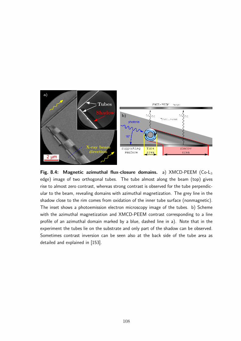
b)
X-ray beamdirection
a)
Shadow
Tubes
Fig. 8.4: Magnetic azimuthal flux-closure domains. a) XMCD-PEEM (Co-L3
edge) image of two orthogonal tubes. The tube almost along the beam (top) givesrise to almost zero contrast, whereas strong contrast is observed for the tube perpendic-ular to the beam, revealing domains with azimuthal magnetization. The grey line in theshadow close to the rim comes from oxidation of the inner tube surface (nonmagnetic).The inset shows a photoemission electron microscopy image of the tubes. b) Schemewith the azimuthal magnetization and XMCD-PEEM contrast corresponding to a lineprofile of an azimuthal domain marked by a blue, dashed line in a). Note that in theexperiment the tubes lie on the substrate and only part of the shadow can be observed.Sometimes contrast inversion can be seen also at the back side of the tube area asdetailed and explained in [153].
108

Note that the tube is multidomain: the sense (sign) of the circulation of theflux-closure alternates along the tube axis. Such tubes provide a key advantageover longitudinally-magnetized systems in the context of devices like the racetrackmemory (Fig. 8.6a), as flux-closure domains would drastically reduce the interactionbetween neighbouring elements via their stray field. The density of domains can bevery high, 5/µm or more, upon demagnetization (Fig. 8.6b). The possibilities ofusing tubular racetracks instead of vertical strips or solid wires are further discussedin chapter 12 (Conclusion & Perspective).
(a) Circular Left (-) (b) Circular Right (+)
Beam
(c) X-ray Magnetic Circular Dichroism
Fig. 8.5: Scanning transmission X-ray microscopy of a CoNiB tube (SS53, tubeAnalena) at the Co-L3 edge (778.1 eV). Even with a single circular polarization one cansee a strong magnetic contrast (difference in absorption): (a) Image for circular left,(b) circular right polarization. (c) illustrates the XMCD (difference of the two beampolarizations). Images obtained on the same batch of tubes one year after the firstXMCD-PEEM beamtime.
8.3 Magnetic anisotropy
Let us now turn to the reason for azimuthal magnetization. We find very similardomains following either AC-field demagnetization along the transverse direction,or saturation along the tube axis. Therefore, the azimuthal curling seems to be theground state for this material and geometry. Recently, Wyss and coworkers [79] ob-served with XMCD-PEEM CoFeB and NiFe nanotubes (around 300 nm in diameter,30 nm tube wall thickness, formed by sputtering on semiconducting nanowires witha hexagonal cross-section). They found the curling state (global vortex) only fortubes shorter than 1-2 µm (our tubes have 20-30 µm); longer tubes displayed axial
109

Beam1µmb)
a)
Fig. 8.6: Tubular magnetic racetracks. a) Scheme: bits of information would becoded by azimuthal domains with opposite circulation of magnetization. Flux-closuredomains significantly reduce the stray field and thus the cross-talk in a dense array oftubes in a potential memory device. b) Experimental shadow XMCD-PEEM image of aCoNiB tube (on Si substrate) with many azimuthal domains. The field of view features28 domains, with some of them being very narrow, not speaking of the domain wallsthemselves. The blue solid line is the approximate boundary between signal coming fromthe tube surface (below) and shadow (above the line).
110

magnetization with the curling only at the tube ends as expected from theory [21].Similarly, our tubes should display axial magnetization (consult magnetization phasediagrams in [21, 76, 77]). Thus, we argue that an additional contribution, magneticanisotropy, has to be present to promote alignment of magnetization in the azimuthaldirection.
First, we provide arguments for describing and extracting the strength of themicroscopic magnetic anisotropy favouring azimuthal magnetization. We start withaddressing a question: What is the functional form relevant to describe the volumedensity of magnetic anisotropy, as none of the three local directions are equivalent(radial 𝑟, azimuthal 𝜑 and axial 𝑧)? Given the large aspect ratio of our tubes,we assume that the local shape anisotropy (i.e. magnetostatic energy) is the dom-inant energy term. This is also justified later by showing that an anisotropy fielddetermined from hysteresis loops is small compared to spontaneous induction (tensof mT and about 1 T, respectively). Further, we suppose zero radial magnetiza-tion (𝑚𝑟 = 0) in magnetic domains (𝑚 = 𝑀
𝑀s). Thus, describing the anisotropy with
terms −𝐾𝜑𝑚2𝜑 or 𝐾𝜑𝑚2
𝑧 should be equivalent, because 𝑚2𝜑 +𝑚2
𝑧 ≈ 1. 𝐾𝜑 > 0 favoursazimuthal magnetization.
On the basis of the moderate wall thickness (30 nm compared to 300 nm diam-eter for our CoNiB tubes; in general valid for thin-walled tubes), we assume thatradius-dependent variations are averaged out and taken into account in an effectiveuniform value of 𝐾𝜑. A first contribution to 𝐾𝜑 is magnetic anisotropy related tothe (crystal) lattice 𝐾m: magnetocrystalline, magnetoelastic or interface anisotropy(to be discussed later in the text). A second contribution is related to the exchangeenergy, whose volume density reads, for 𝑚𝑟 = 0 [21, 214]: 𝐸ex = (𝐴/𝑅2)𝑚2
𝜑 with𝐴 being the exchange stiffness constant and 𝑅 the tube radius. The term reflectscurvature-induced anisotropy that forces �� to deviated from the azimuthal direc-tion (and lie e.g. in the axial direction): curvature induces a spatial variation ofmagnetization for a uniform 𝑚𝜑, due to the non-uniformity of 𝜑. Uniform 𝑚𝑧 isassociated with no spatial variation, so it does not contribute. The exchange con-tribution leads to axial magnetization in nanotubes with small diameters as alreadyshown in the magnetization phase diagrams (see Fig. 3.2). The total anisotropycoefficient is 𝐾𝜑 = 𝐾m − 𝐴/𝑅2. This can be converted into an anisotropy field𝐻𝐾 = 2𝐾𝜑/(𝜇0𝑀s). Measuring the latter experimentally allows one to estimate themicroscopic anisotropy energy coefficient: 𝐾m = 𝐴/𝑅2 + 𝜇0𝑀s𝐻𝐾/2.
Now we will introduce measurements of CoNiB tubes under external magneticfield, enabling determination of the anisotropy field and thus estimation of theanisotropy coefficient 𝐾m. Later we return to the question of origin of the anisotropy(magnetocrystalline, magnetetoelastic, interface, . . . ), effect of a thermal annealing,material composition and geometry on the magnetization direction in the domains.
111
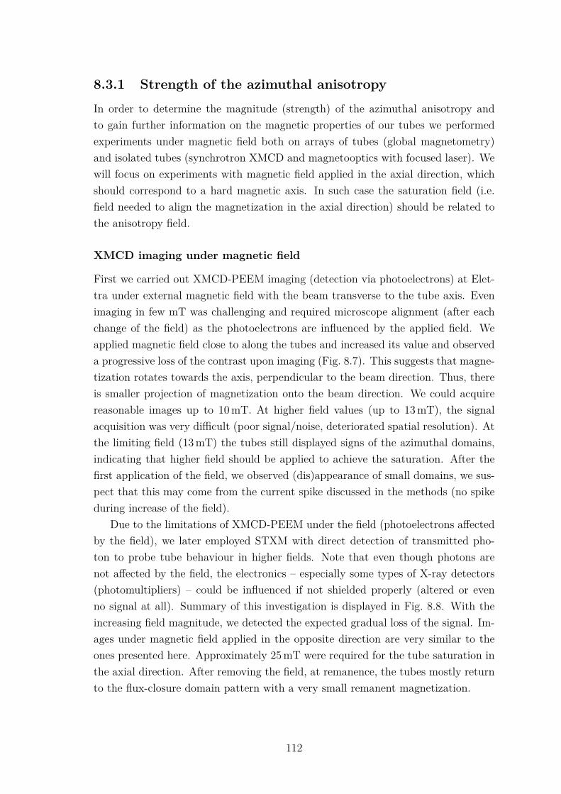
8.3.1 Strength of the azimuthal anisotropy
In order to determine the magnitude (strength) of the azimuthal anisotropy andto gain further information on the magnetic properties of our tubes we performedexperiments under magnetic field both on arrays of tubes (global magnetometry)and isolated tubes (synchrotron XMCD and magnetooptics with focused laser). Wewill focus on experiments with magnetic field applied in the axial direction, whichshould correspond to a hard magnetic axis. In such case the saturation field (i.e.field needed to align the magnetization in the axial direction) should be related tothe anisotropy field.
XMCD imaging under magnetic field
First we carried out XMCD-PEEM imaging (detection via photoelectrons) at Elet-tra under external magnetic field with the beam transverse to the tube axis. Evenimaging in few mT was challenging and required microscope alignment (after eachchange of the field) as the photoelectrons are influenced by the applied field. Weapplied magnetic field close to along the tubes and increased its value and observeda progressive loss of the contrast upon imaging (Fig. 8.7). This suggests that magne-tization rotates towards the axis, perpendicular to the beam direction. Thus, thereis smaller projection of magnetization onto the beam direction. We could acquirereasonable images up to 10 mT. At higher field values (up to 13 mT), the signalacquisition was very difficult (poor signal/noise, deteriorated spatial resolution). Atthe limiting field (13 mT) the tubes still displayed signs of the azimuthal domains,indicating that higher field should be applied to achieve the saturation. After thefirst application of the field, we observed (dis)appearance of small domains, we sus-pect that this may come from the current spike discussed in the methods (no spikeduring increase of the field).
Due to the limitations of XMCD-PEEM under the field (photoelectrons affectedby the field), we later employed STXM with direct detection of transmitted pho-ton to probe tube behaviour in higher fields. Note that even though photons arenot affected by the field, the electronics – especially some types of X-ray detectors(photomultipliers) – could be influenced if not shielded properly (altered or evenno signal at all). Summary of this investigation is displayed in Fig. 8.8. With theincreasing field magnitude, we detected the expected gradual loss of the signal. Im-ages under magnetic field applied in the opposite direction are very similar to theones presented here. Approximately 25 mT were required for the tube saturation inthe axial direction. After removing the field, at remanence, the tubes mostly returnto the flux-closure domain pattern with a very small remanent magnetization.
112
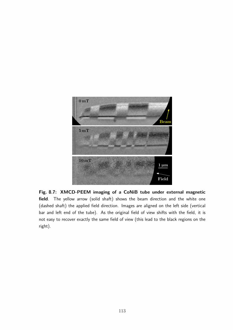
1µm
0mT
5mT
10mT
Beam
Field
Fig. 8.7: XMCD-PEEM imaging of a CoNiB tube under external magneticfield. The yellow arrow (solid shaft) shows the beam direction and the white one(dashed shaft) the applied field direction. Images are aligned on the left side (verticalbar and left end of the tube). As the original field of view shifts with the field, it isnot easy to recover exactly the same field of view (this lead to the black regions on theright).
113
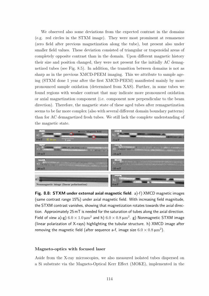
We observed also some deviations from the expected contrast in the domains(e.g. red circles in the STXM image). They were most prominent at remanence(zero field after previous magnetization along the tube), but present also undersmaller field values. These deviation consisted of triangular or trapezoidal areas ofcompletely opposite contrast than in the domain. Upon different magnetic historytheir size and position changed, they were not present for the initially AC demag-netized tubes (see Fig. 8.5). In addition, the transition between domains is not assharp as in the previous XMCD-PEEM imaging. This we attribute to sample age-ing (STXM done 1 year after the first XMCD-PEEM) manifested mainly by morepronounced sample oxidation (determined from XAS). Further, in some tubes wefound regions with weaker contrast that may indicate more pronounced oxidationor axial magnetization component (i.e. component now perpendicular to the beamdirection). Therefore, the magnetic state of these aged tubes after remagnetizationseems to be far more complex (also with several different domain boundary patterns)than for AC demagnetized fresh tubes. We still lack the complete understanding ofthe magnetic state.
0 mT -5 mT
-10 mT -15 mT
-20 mT -25 mT
0 mTNonmagnetic image (linear polarization)
a)
c)
e)
g)
b)
d)
f)
h)
Beam
Magnetic field
1 µm
Fig. 8.8: STXM under external axial magnetic field. a)-f) XMCD magnetic images(same contrast range 15%) under axial magnetic field. With increasing field magnitude,the STXM contrast vanishes, showing that magnetization rotates towards the axial direc-tion. Approximately 25 mT is needed for the saturation of tubes along the axial direction.Field of view a)-g) 6.0 × 1.0µm2 and h) 6.0 × 0.8µm2. g) Nonmagnetic STXM image(linear polarization of X-rays) highlighting the tubular structure. h) XMCD image afterremoving the magnetic field (after sequence a-f, image size 6.0 × 0.8µm2).
Magneto-optics with focused laser
Aside from the X-ray microscopies, we also measured isolated tubes dispersed ona Si substrate via the Magneto-Optical Kerr Effect (MOKE), implemented in the
114
longitudinal configuration with a focused He-Ne (𝜆 = 632.8 nm) laser (spot 1 µm).The field was swept as a triangular wave signal, with frequency 1.1 Hz, and field cal-ibration uncertainty max ±5 mT. For the measurements presented below, the laserpower was 1.1 mW, for some measurements we used just 0.2 mW. Fig. 8.9 shows hys-teresis loops obtained on the tubes. Some loops are slanted (Fig. 8.9a) with almostno remanence (tube axis = hard axis for magnetization) which is consistent with thesynchrotron data, where magnetization is azimuthal at remanence (perpendicular tothe tube axis) and under axial field gradually rotates towards the axis (see Fig. 8.8).However, in some cases (different tubes, even different tube part in one instance)the loops are quite squared (Fig. 8.9b).
c)
d)
5µm
b)a)
Tube 1 Tube 2
Fig. 8.9: Magnetometry on a single tube - magnetooptics with focused laser.Hysteresis loops for the axial magnetic field (longitudinal MOKE): a) slanted curve, b)rather squared loop obtained on another tube. Average of 100 loops with a short acqui-sition time (0.9 s). Data processed in OriginPro: line subtracted, normalized, smoothed:average of 7 adjacent points (red curve) – original curve had 5000 points (black points).c) Optical image (magnification 100x) of a tube with the diffracted laser spot, the mag-netic field is applied in the horizontal direction, close to parallel to the tube axis. d)Scanning electron microscopy image of a central part of the tube from c).
This was also the case when one tube (previously non-irradiated) was probedwith just 0.2 mW laser power – close to the minimum power we can apply andmeasure some magnetic signal for tubes in our setup. We assume that the loopsquareness is caused by a laser heating due to a bad thermal contact with the sub-strate for some tubes. As tubes are dispersed from a solution, template dissolutionproducts may create a halo around structures and decrease the thermal conduc-tivity of the contact. In addition, in case of tubes (cylindrical objects in general)the contact area is rather small. Hysteresis loops acquired with higher laser powershow larger squareness. Further, the signal is higher, but less stable (drift). Forthe power of several mW and longer time exposure, we noticed that some of ourtubes are damaged – see annex A.2. Only several tubes were measured with MOKE
115
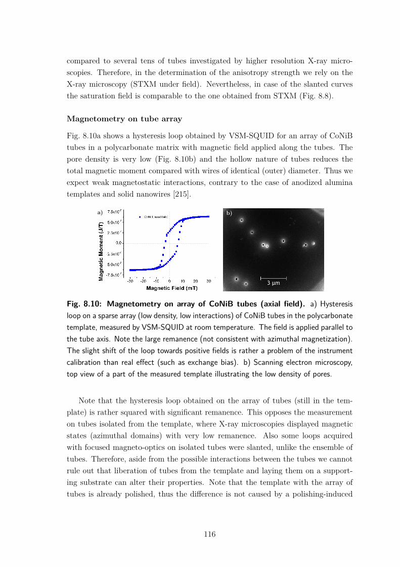
compared to several tens of tubes investigated by higher resolution X-ray micro-scopies. Therefore, in the determination of the anisotropy strength we rely on theX-ray microscopy (STXM under field). Nevertheless, in case of the slanted curvesthe saturation field is comparable to the one obtained from STXM (Fig. 8.8).
Magnetometry on tube array
Fig. 8.10a shows a hysteresis loop obtained by VSM-SQUID for an array of CoNiBtubes in a polycarbonate matrix with magnetic field applied along the tubes. Thepore density is very low (Fig. 8.10b) and the hollow nature of tubes reduces thetotal magnetic moment compared with wires of identical (outer) diameter. Thus weexpect weak magnetostatic interactions, contrary to the case of anodized aluminatemplates and solid nanowires [215].
b)a)
Fig. 8.10: Magnetometry on array of CoNiB tubes (axial field). a) Hysteresisloop on a sparse array (low density, low interactions) of CoNiB tubes in the polycarbonatetemplate, measured by VSM-SQUID at room temperature. The field is applied parallel tothe tube axis. Note the large remanence (not consistent with azimuthal magnetization).The slight shift of the loop towards positive fields is rather a problem of the instrumentcalibration than real effect (such as exchange bias). b) Scanning electron microscopy,top view of a part of the measured template illustrating the low density of pores.
Note that the hysteresis loop obtained on the array of tubes (still in the tem-plate) is rather squared with significant remanence. This opposes the measurementon tubes isolated from the template, where X-ray microscopies displayed magneticstates (azimuthal domains) with very low remanence. Also some loops acquiredwith focused magneto-optics on isolated tubes were slanted, unlike the ensemble oftubes. Therefore, aside from the possible interactions between the tubes we cannotrule out that liberation of tubes from the template and laying them on a support-ing substrate can alter their properties. Note that the template with the array oftubes is already polished, thus the difference is not caused by a polishing-induced
116
strain. On the other hand, the polishing is not perfect and parts of the top/bot-tom film on the template are still present (few patches visible also in Fig. 8.10b).Despite this unpolished area being small, we cannot rule out its contribution in themagnetometry.
Determination of the anisotropy strength
Experimentally, we estimated the anisotropy field 𝐻𝐾 based on the series of scanningtransmission X-ray microscopy images acquired under different external magneticfield applied along the tube axis (Fig. 8.8). Upon increasing the field, the domaincontrast decreases, which shows that magnetization gradually rotates towards theaxial direction. Therefore, such behaviour would correspond to hysteresis loop mea-sured for hard axis – slanted curve with zero remanence (such as in Fig. 8.9a). Insuch case the anisotropy and saturation fields are closely related. Even-though themethod cannot give a precise measurement of the anisotropy, it still enables us toobtain reasonable estimate of the anisotropy. It is difficult to extract quantitativelythe direction of magnetization in series of STXM, because of the exponential decayof photon intensity inside matter, uncertainties in the dichroic coefficient, and theexistence of a background intensity in the image. We can only provide an estimateof the 𝐻𝐾 from the fields where all contrast vanishes in the corresponding images.We find 𝜇0𝐻𝐾 ≈ 25 mT.
As regards the conversion of 𝐻𝐾 to the anisotropy constant, we do not have adirect measurement of the exchange stiffness of our material, however for exampleCo80B20 has 𝐴 ≈ 10 pJ/m [216]. This value may be different in our case, but the or-der of magnitude should be correct. Besides, the tube diameter is large, so that theexchange penalty correction to the anisotropy is rather small, less than few mT ofequivalent field, which might be well within the error/spread of the experimentallydetermined anisotropy field. Further, similar to the curvature-induced anisotropy(exchange contribution), curvature-induced effective Dzyaloshinskii-Moriya interac-tion is expected to be negligible as it also scales with the curvature, being morepronounced for tube diameters below 100 nm. Therefore, we arrive at an estimate ofthe anisotropy constant 𝐾m ≈ 10 kJ/m3. However, this value may be affected by asample ageing (discussed further in section 8.3.5). The one-year-old sample, initiallyused for XMCD-PEEM and later for STXM, shows less sharp azimuthal domainsand a weak axial component of the magnetization, although it has been kept underprimary vacuum. Therefore, the initial value (giving well defined azimuthal domainswith Bloch like domain walls), may have been higher (i.e. tens of kJ/m3).
117
8.3.2 Origin of the azimuthal anisotropy
As our tubes are cobalt-rich, the first contribution coming to mind is the magne-tocrystalline anisotropy. However, as our tubes are nanocrystalline with a randomtexture (see diffraction rings in Fig. 8.1b), we rule out the magnetocrystalline contri-bution. There must be another source of magnetic energy, for which the degeneracybetween the axial 𝑧 and the azimuthal 𝜑 direction is lifted. While both directionsare normal to the radial direction 𝑟, and are thus locally similar to two the in-planedirection for a thin film, the difference is the existence of curvature along the az-imuthal direction. We consider below two possible sources of magnetic anisotropythat could arise from the direction-dependent curvature: intergranular interfaceanisotropy and magneto-elastic coupling (inverse magnetostriction). Owing to theradial growth process (Fig. 4.3), grains are expected to have their shape and sizevarying differently along the two directions. We detail below handwaving models,and show that both sources could in some cases provide a strength of anisotropywhose order of magnitude is consistent with the experimental data.
Interface anisotropy
As our samples are nanocrystalline, the proportion of atoms in the vicinity of agrain/cluster boundary is not negligible, so that interface anisotropy 𝐾s with e.g.boron-rich grain boundaries could arise. We consider a tube with outer diameter250 nm and wall thickness 25 nm. Assuming an isotropic grain size 𝑙0 upon nu-cleation from the outer diameter, the azimuthal grain size 𝑙𝜑 at the inner diametershould be reduced by 20 % (outer radius 125 nm, inner one 100 nm and thus (125 nm-100 nm)/125 nm=0.2; the grain size along the azimuth is directly proportional to theradius). We further assume that the grain size along the tube axis 𝑙𝑧 stays almostconstant (some small tensile strain is possible as a result of compressive strain in theradial direction). Thus on the average along the radius the anisotropy of grain size𝛿 = ⟨𝑙𝑧⟩−⟨𝑙𝜑⟩
(⟨𝑙𝑧⟩+⟨𝑙𝜑⟩)/2is 0.1, yielding a slightly wedge-shaped grain (such as in Fig. 4.3c);
⟨𝑙𝜑⟩ = 0.9𝑙0, ⟨𝑙𝑧⟩ = 1𝑙0 being average grain sizes along the azimuth and the tubeaxis, respectively, and 𝑙0 is the grain size on the outer surface. Transmission elec-tron microscopy suggests that the grain size is of the order of 𝑡 = 10 nm. Theanisotropic contribution of 𝐾s to the effective volume magnetic anisotropy 𝐾eff is2𝛿𝐾s/𝑡. Considering 𝐾s ≈ 0.2 mJ/m2 as an estimate (values nearly one order ofmagnitude higher may exist at some interfaces, for instance between 3d elementsand some oxides [217]), one finds: 𝐾eff ≈ 4 · 103 J/m3. Expressed as the anisotropyfield: 𝐻eff ≈ 2𝐾eff/(𝜇0𝑀s) = 8 · 103 A/m or 𝜇0𝐻eff ≈ 10 mT. This is of the same or-der of magnitude as the measured value of 25 mT. Another contribution of interfaceanisotropy may be due to the curvature of the outer and inner parts of the grains,
118

so that the orientation of atomic bounds is on the average slightly different alongthe axial and azimuthal directions. A proper modelling would, however, requireadvanced information about the structure of the interface, which is not available.
Magnetoelastic anisotropy
Borides of 3d ferromagnetic elements are known to display sizeable magnetoelasticeffects [218] (except for few particular compositions, e.g. (Ni80Fe20)B with almostzero magnetostriction), and electroless plating is also known to deliver strainedmaterials. It is probable that the expected wedged shape of the grains describedabove (also see Fig. 4.3c), induce a building of higher compressive strain 𝜖 along 𝜑
while the grain grows inward, because there is less and less space to accommodateincoming atoms. Tensile strain along 𝑧 may be expected from elastic theory, as areaction to the compressive along 𝜑. An extra isotropic strain in the (𝜑, 𝑧) planemay also be expected from the electroless deposition. Further strain may comefrom the rapid dissolution of the polycarbonate template used for the fabricationof tubes. The saturation magnetostriction of Co-rich CoNi borides is of the orderof 𝜆 ≈ −6 · 10−6, more values with references can be found in Tab. 8.1. For 3dmetals the combination of elastic coefficients 𝑐11 − 𝑐12 is of the order of 10−11 N/m2,or 10−11 J/m3. Thus, the linear magnetoelastic coefficient is 𝐵1 ≈ −106 J/m3. Ananisotropy of strain of 0.4 % would therefore be required to account for the observedmicroscopic anisotropy.
Considering our fabrication method, material and comparison with NiFeB tubesin the following section, we would like to put forward the magnetoelastic coupling asmore likely source of the anisotropy. Most of electroless-deposited films are strained,even on a flat substrate. Fig. 8.11 shows an extreme case of thicker CoNiB film wedeposited on a Si substrate. Internal stress was relaxed by formation of micro-and nano-cracks, delaminating parts of the film and partially rolling it, sometimesforming "Swiss rolls". Streubel et al. [94] used more controlled strain engineeringto fabricate similar "microtubes" (but with better defined geometry). Some degreeof strain is expected also for smaller thickness; curved tube surface [34] and radialdeposition in confined pores (Fig. 4.3) can only enhance this effect.
To conclude this part, electroless-grown materials are expected to develop na-nograins with some anisotropic structure features along the radial and azimuthaldirections, associated with the local curvature of the supporting surface, be it shapeor strain. The resulting contribution to magnetic anisotropy could arise from bothinterface anisotropy and magnetoelastic coupling. Realistic figures show that bothsources could explain the experimental results. Having in mind comparison withNiFeB tubes below, we would put forward the magnetoelasticity. However, without
119

Fig. 8.11: Thick CoNiB electroless-deposited film on a Si substrate. The internalstress is relaxed by cracks in the film as well as delamination and rolling parts of thefilm, sometimes forming Swiss rolls or tube-like structures. Here an extreme case with2 µm thick film is shown, but some degree of internal strain is expected for smallerthickness (delamination and rolling was not observed for films below 100 nm provided byTU Darmstadt).
further knowledge on the structural anisotropy of the nanograins, which would bechallenging to access, it is not possible to decide unambiguously which phenomenonis dominating.
8.3.3 Comparison with NiFeB tubes
For comparison we also considered nanocrystalline electroless-plated tubes with verysimilar geometry (diameter 350-390 nm) but from (Ni80Fe20)B. These proved to beaxially magnetized (Fig. 8.12, see also electron holography in Fig 8.13). The dif-ference between the two materials is the strength of the magnetostriction, which issizeable and negative for (Co80Ni20)B (Tab. 8.1), and nearly vanishing and positivefor (Ni80Fe20)B [218]. In addition, Fe-based alloys are also known to display lowerinterfacial anisotropy. In other words, both above-discussed anisotropy sources areexpected to be weaker in magnitude for NiFeB tubes. Thus, it is not surprising torecover the axial magnetic state predicted by theory in tubes made of a magnetically-soft material.
We further investigated NiFeB tubes (SS123 sample from TU Darmstadt) withelectron holography. Based upon previous synchrotron measurements on NiFeBshells, we expected uniform axial magnetization everywhere. Indeed phase mapsindicating axial component of the magnetic induction were acquired. With the helpof magnetic field we could saturate the tube along the two opposite axial directions(imaging at remanence) and we observed phase gradients similar to the case of
120
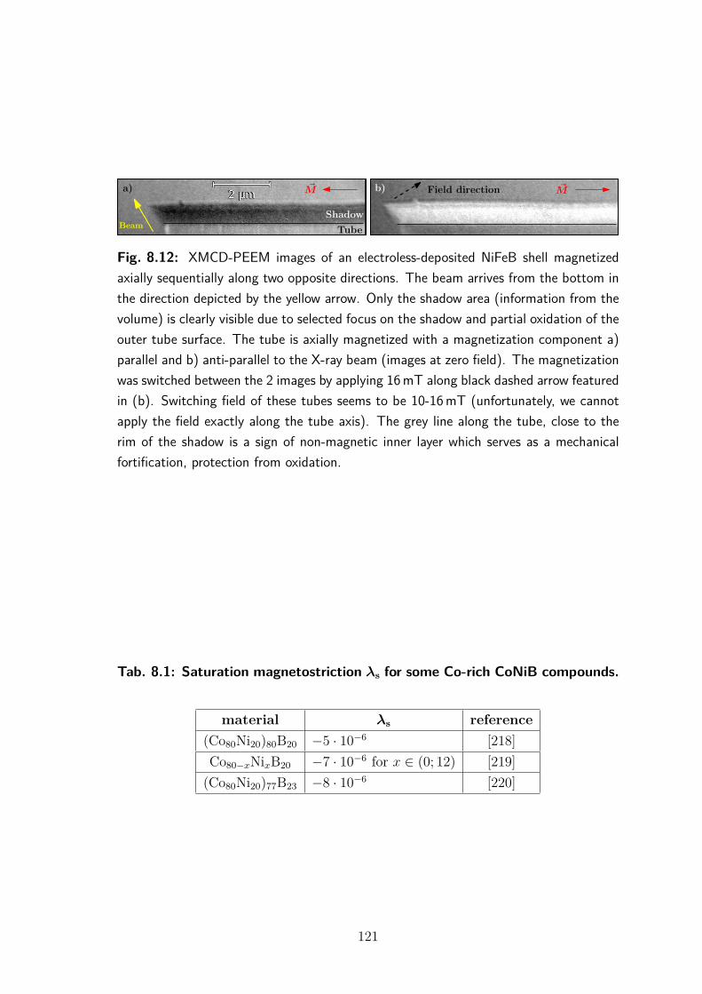
b)
Tube
Shadow
a)
Beam
~M ~MField direction
Fig. 8.12: XMCD-PEEM images of an electroless-deposited NiFeB shell magnetizedaxially sequentially along two opposite directions. The beam arrives from the bottom inthe direction depicted by the yellow arrow. Only the shadow area (information from thevolume) is clearly visible due to selected focus on the shadow and partial oxidation of theouter tube surface. The tube is axially magnetized with a magnetization component a)parallel and b) anti-parallel to the X-ray beam (images at zero field). The magnetizationwas switched between the 2 images by applying 16 mT along black dashed arrow featuredin (b). Switching field of these tubes seems to be 10-16 mT (unfortunately, we cannotapply the field exactly along the tube axis). The grey line along the tube, close to therim of the shadow is a sign of non-magnetic inner layer which serves as a mechanicalfortification, protection from oxidation.
Tab. 8.1: Saturation magnetostriction 𝜆s for some Co-rich CoNiB compounds.
material 𝜆s reference(Co80Ni20)80B20 −5 · 10−6 [218]Co80−𝑥Ni𝑥B20 −7 · 10−6 for 𝑥 ∈ (0; 12) [219]
(Co80Ni20)77B23 −8 · 10−6 [220]
121

nanowires (Fig. 8.13).
~M ~M
300 nm
Fig. 8.13: Electron holography on a NiFeB SS123 electroless tube (diameteraround 300 nm) with opposite magnetization. Wrapped phase maps show the tubesaturated by external magnetic field in two opposite axial direction. Both electrostaticand magnetic parts are present. Compare with the nanowire case in Fig. 5.12.
Initially, magnetization at the tube ends was mostly uniform, pointing alongthe tube axis; similar behaviour was observed in XMCD-PEEM experiments. Butafter applying the transverse field, the end curling appeared (Fig. 8.14, right end),similar to the one observed by Diehle et al. [109] and with extend matching thepredictions in [79] for the given tube diameter. The interesting point is that theend curling is expected to develop in such larger diameter tubes, as the mixedstate (axial magnetization with end curling) has lower energy than having axialmagnetization everywhere (see the limitation of the "F" state to small diameters inFig. 3.2). Further, we continued also as in case of the nanowires with modulateddiameter: we tried to nucleate a DW with a transverse magnetic field having also asmall axial component. We did not observe well-separated opposite domains with adomain wall in between. Instead, complex phase patterns were present. This mightbe caused by the large tube diameter (300-400 nm). Experiments on nanotubes withsmaller diameter and pure axial field could provide better results.
300 nm
Fig. 8.14: Electron holography on a NiFeB SS123 electroless tube (diameteraround 300 nm) after saturation in a nearly transverse direction. Image at rema-nence close to the tube end. Both electrostatic and magnetic parts are present. On theright end of the tube one can see pattern that could be assigned to end curling typicallypresent in large diameter tubes. To the left we expected pattern for axial magnetizationsuch as in Fig. 8.13, i.e. with contour lines along the tube. However, a different patternis present instead.
122
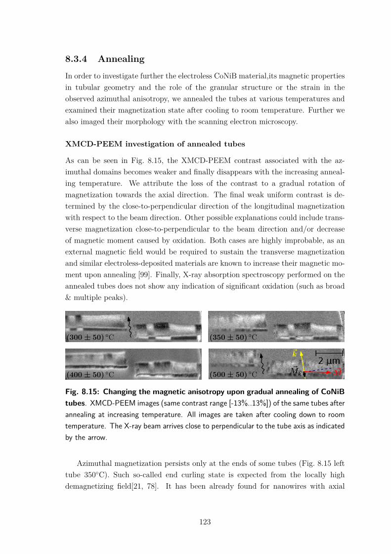
8.3.4 Annealing
In order to investigate further the electroless CoNiB material,its magnetic propertiesin tubular geometry and the role of the granular structure or the strain in theobserved azimuthal anisotropy, we annealed the tubes at various temperatures andexamined their magnetization state after cooling to room temperature. Further wealso imaged their morphology with the scanning electron microscopy.
XMCD-PEEM investigation of annealed tubes
As can be seen in Fig. 8.15, the XMCD-PEEM contrast associated with the az-imuthal domains becomes weaker and finally disappears with the increasing anneal-ing temperature. We attribute the loss of the contrast to a gradual rotation ofmagnetization towards the axial direction. The final weak uniform contrast is de-termined by the close-to-perpendicular direction of the longitudinal magnetizationwith respect to the beam direction. Other possible explanations could include trans-verse magnetization close-to-perpendicular to the beam direction and/or decreaseof magnetic moment caused by oxidation. Both cases are highly improbable, as anexternal magnetic field would be required to sustain the transverse magnetizationand similar electroless-deposited materials are known to increase their magnetic mo-ment upon annealing [99]. Finally, X-ray absorption spectroscopy performed on theannealed tubes does not show any indication of significant oxidation (such as broad& multiple peaks).
(300 ± 50) ◦C (350 ± 50) ◦C
(400 ± 50) ◦C (500 ± 50) ◦C ~M
~k
~M~k
Fig. 8.15: Changing the magnetic anisotropy upon gradual annealing of CoNiBtubes. XMCD-PEEM images (same contrast range [-13%..13%]) of the same tubes afterannealing at increasing temperature. All images are taken after cooling down to roomtemperature. The X-ray beam arrives close to perpendicular to the tube axis as indicatedby the arrow.
Azimuthal magnetization persists only at the ends of some tubes (Fig. 8.15 lefttube 350∘C). Such so-called end curling state is expected from the locally highdemagnetizing field[21, 78]. It has been already found for nanowires with axial
123
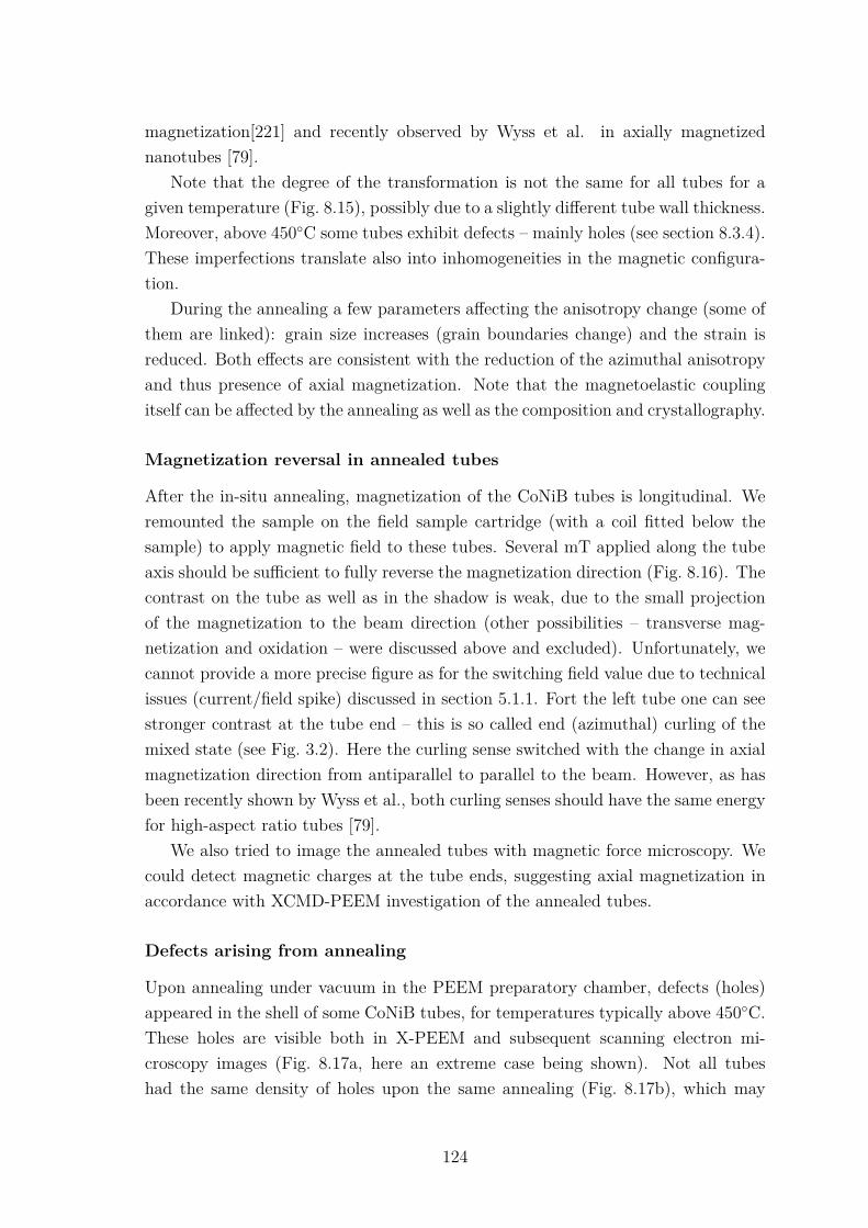
magnetization[221] and recently observed by Wyss et al. in axially magnetizednanotubes [79].
Note that the degree of the transformation is not the same for all tubes for agiven temperature (Fig. 8.15), possibly due to a slightly different tube wall thickness.Moreover, above 450∘C some tubes exhibit defects – mainly holes (see section 8.3.4).These imperfections translate also into inhomogeneities in the magnetic configura-tion.
During the annealing a few parameters affecting the anisotropy change (some ofthem are linked): grain size increases (grain boundaries change) and the strain isreduced. Both effects are consistent with the reduction of the azimuthal anisotropyand thus presence of axial magnetization. Note that the magnetoelastic couplingitself can be affected by the annealing as well as the composition and crystallography.
Magnetization reversal in annealed tubes
After the in-situ annealing, magnetization of the CoNiB tubes is longitudinal. Weremounted the sample on the field sample cartridge (with a coil fitted below thesample) to apply magnetic field to these tubes. Several mT applied along the tubeaxis should be sufficient to fully reverse the magnetization direction (Fig. 8.16). Thecontrast on the tube as well as in the shadow is weak, due to the small projectionof the magnetization to the beam direction (other possibilities – transverse mag-netization and oxidation – were discussed above and excluded). Unfortunately, wecannot provide a more precise figure as for the switching field value due to technicalissues (current/field spike) discussed in section 5.1.1. Fort the left tube one can seestronger contrast at the tube end – this is so called end (azimuthal) curling of themixed state (see Fig. 3.2). Here the curling sense switched with the change in axialmagnetization direction from antiparallel to parallel to the beam. However, as hasbeen recently shown by Wyss et al., both curling senses should have the same energyfor high-aspect ratio tubes [79].
We also tried to image the annealed tubes with magnetic force microscopy. Wecould detect magnetic charges at the tube ends, suggesting axial magnetization inaccordance with XCMD-PEEM investigation of the annealed tubes.
Defects arising from annealing
Upon annealing under vacuum in the PEEM preparatory chamber, defects (holes)appeared in the shell of some CoNiB tubes, for temperatures typically above 450∘C.These holes are visible both in X-PEEM and subsequent scanning electron mi-croscopy images (Fig. 8.17a, here an extreme case being shown). Not all tubeshad the same density of holes upon the same annealing (Fig. 8.17b), which may
124
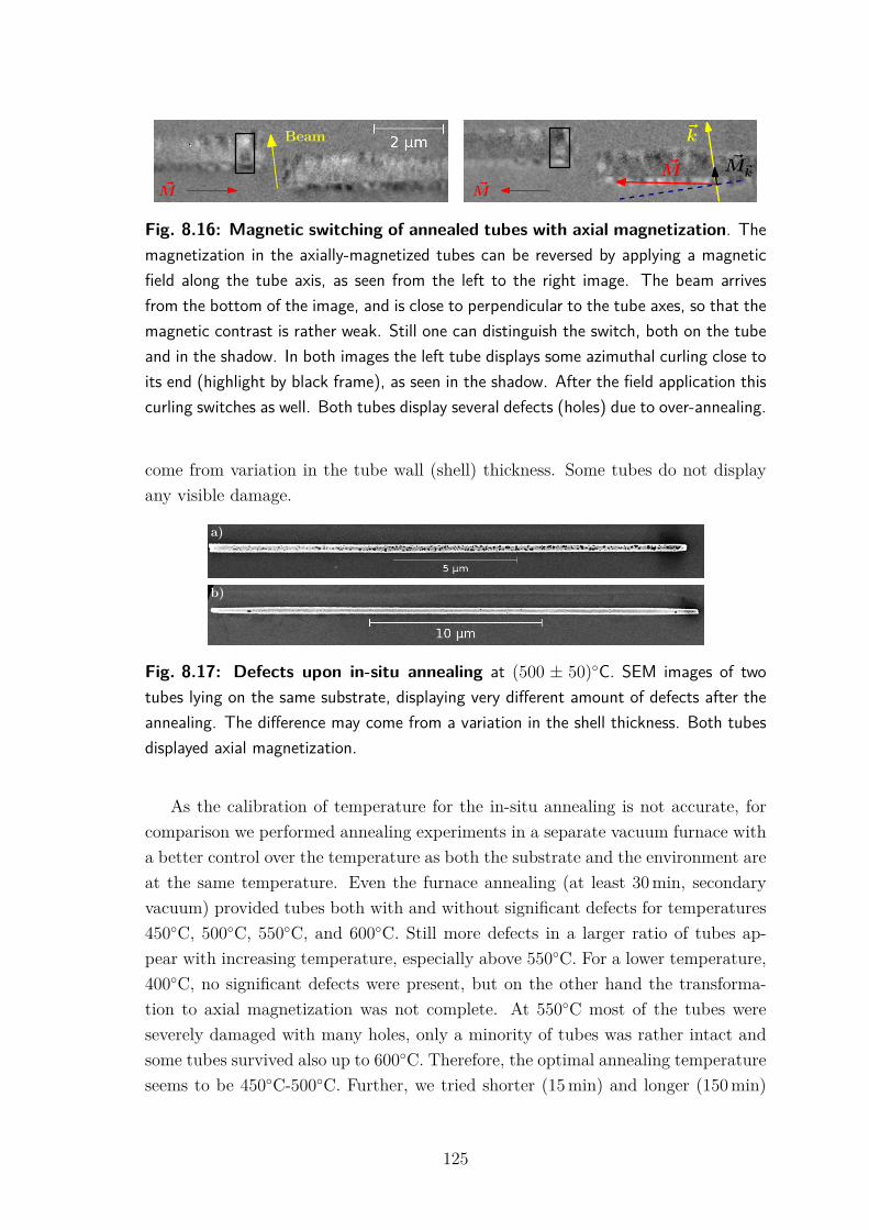
Beam
~M ~M
~M
~k
~M~k
Fig. 8.16: Magnetic switching of annealed tubes with axial magnetization. Themagnetization in the axially-magnetized tubes can be reversed by applying a magneticfield along the tube axis, as seen from the left to the right image. The beam arrivesfrom the bottom of the image, and is close to perpendicular to the tube axes, so that themagnetic contrast is rather weak. Still one can distinguish the switch, both on the tubeand in the shadow. In both images the left tube displays some azimuthal curling close toits end (highlight by black frame), as seen in the shadow. After the field application thiscurling switches as well. Both tubes display several defects (holes) due to over-annealing.
come from variation in the tube wall (shell) thickness. Some tubes do not displayany visible damage.
a)
b)
Fig. 8.17: Defects upon in-situ annealing at (500 ± 50)∘C. SEM images of twotubes lying on the same substrate, displaying very different amount of defects after theannealing. The difference may come from a variation in the shell thickness. Both tubesdisplayed axial magnetization.
As the calibration of temperature for the in-situ annealing is not accurate, forcomparison we performed annealing experiments in a separate vacuum furnace witha better control over the temperature as both the substrate and the environment areat the same temperature. Even the furnace annealing (at least 30 min, secondaryvacuum) provided tubes both with and without significant defects for temperatures450∘C, 500∘C, 550∘C, and 600∘C. Still more defects in a larger ratio of tubes ap-pear with increasing temperature, especially above 550∘C. For a lower temperature,400∘C, no significant defects were present, but on the other hand the transforma-tion to axial magnetization was not complete. At 550∘C most of the tubes wereseverely damaged with many holes, only a minority of tubes was rather intact andsome tubes survived also up to 600∘C. Therefore, the optimal annealing temperatureseems to be 450∘C-500∘C. Further, we tried shorter (15 min) and longer (150 min)
125
annealing time for 450∘C. 15 min led to almost no defects, but the increase of thegrains size with respect to the as-deposited sample was very small, suggesting thatlonger annealing is needed. Longer (150 min) experiment produced slightly moredefects such as tubes broken in places where there were already some small defects.
Now we will briefly mention possible differences in experimental conditions be-tween annealing done inside the PEEM system (in-situ annealing) and the vacuumfurnace annealing but we do not suppose that they play a significant role. ThePEEM preparation chamber is operated under ultra-high vacuum. However, duringthe annealing the pressure increases substantially and it is of the same order of mag-nitude as the pressure in the vacuum furnace (secondary vacuum, < 10−4 Pa). Themain difference might be X-ray beam irradiation of some tubes before the anneal-ing, in particular effect of the X-rays on the tubes and impurities that cover them(breaking bonds, graphitizing hydrocarbons, etc.). As only part of the sample wasirradiated, but the whole sample was annealed, we could conclude that there is nobig difference between irradiated tubes and tubes not exposed to X-rays (based onelectron microscopy images of both sets of tubes). As we used twin samples on thesame substrates in both (in-situ, furnace) annealing experiments, we suppose thatboth are comparable.
The presence of larger defects (especially above 450∘C) can be an issue as theylead to inhomogeneity in the magnetic configuration. We tried to tackle this problemby fortifying the tubes with an additional inner (non-magnetic) layer deposited eitherby electroless plating or atomic layer deposition (ALD). It seems that the amountof defects in such tubes upon annealing is lower. Alternatively it is possible toperform the ALD after dispersion of tubes on the substrate – this improves notonly mechanical stability, but also protects the tubes from further oxidation. Butwe refrained from such treatment as the electrically-insulating oxide cover layercan cause problems (charging) in collection of the photoelectrons in XMCD-PEEMunless it is very thin.
8.3.5 Sample ageing
In this section we will look further at aged CoNiB tubes. These are the tubes fromthe same batch as the ones investigated with XMCD-PEEM. However, at the timeof the measurements presented below, they were almost one and half years old, i.e.even older than tubes observed with STXM where some changes in the magneticstate were already noticed. Despite being kept under primary vacuum for most of thetime, they are partially oxidized (determined from X-ray absorption spectroscopy),mainly the inner surface as we could already observe in the shadow of XMCD-PEEM images for some tubes (e.g. Fig. 8.7 – grey line in the tube shadow of the
126

top tube). The outer surface is better protected as the tubes were stored still in thepolycarbonate template. The ageing seems to have an effect on the anisotropy andmagnetic configuration in the tubes as will be shown in following images obtainedby electron holography and magnetic force microscopy.
Electron holography on aged CoNiB tubes
For a tube with azimuthal domains and thus perfect flux-closure we would expect nomagnetic signal in electron holography phase maps. Magnetization perpendicular tothe beam is opposite in upper and bottom part of the tube and thus its contributioncancels out; magnetization along the beam does not affect the electron wave (there isno Lorentz force on the electron). Therefore, the signal, if present, could come onlyfrom domain walls or defects. However, as mentioned above, we have indicationsthat there is some axial magnetization component in the domains that should bevisible in the phase maps.
In our electron holography experiments, unlike in simulations (see annex sec-tion B.3), a contrast clearly not of electrostatic origin (compare with Fig. S4)was observed almost everywhere in several tubes, indicating the presence of anin-plane/axial component of the magnetization (see Fig. 8.18).
Fig. 8.18: Experimental wrapped phase maps (both magnetic and electrostaticpart) of CoNiB electroless tubes (SS53, diameter 300 nm). On many places clearaxial component of magnetic induction can be seen (compare to for example previousexperiments on nanowires – Fig. 5.12). Also several strange pattern appeared, these areat least partially of magnetic origin.
Further in some cases, we could remove the electrostatic part by processing im-ages with a flipped sample (magnetic contribution reverses, electrostatic one remainsthe same) and obtain pure non-zero magnetic contribution (e.g. Fig 8.19), some-times even displaying weak stray field from some tube parts – tube ends and alsofrom parts far from the ends or structural defects (domain walls?).
Therefore, flux-closure is indeed not perfect, which we relate to the sample age-ing. If we assume that the spontaneous induction did not decreased significantly(approx. 1 T for fresh CoNiB thin films), then the integrated measured inductionwould correspond to a magnetization being predominantly 80∘ from the tube axis.
127

(a) (b) (c)
Fig. 8.19: Electron holography – magnetic phase maps for a CoNiB tube part(tube diameter around 300 nm, shell thickness 30 nm). (a) continuous magnetic phasemap with integrated in-plane magnetic induction values. (b) corresponding area withamplified magnetic phase – cos 𝜑. (c) Small scheme indicating possible deviation ofmagnetization from in-plane (axial, horizontal) direction, the modelling is tentative andthe angle could be exaggerated.
However, the integrated in-plane induction varies along the tube. As both thediameter and shell thickness seem to be rather uniform, it may reflect that the mag-netization has a larger in-plane component – see model by Aurélien Masseboeuf inFig. 8.20.
Azimuthal state Tilted state Axial state
3D model
top view
cosφm
signal
Fig. 8.20: Electron holography – expected magnetic phase for different mag-netic configurations in a tube. A schematic model by Aurélien Masseboeuf depictingexpected amplified magnetic phase (cos 𝜑 instead of 𝜑) for magnetic configuration havingdifferent axial magnetization component.
In addition, several different phase patterns appeared, some of them might beascribed to domains walls (Fig. 8.21, note that both magnetic and electrostaticparts are present), but probably not simply to Bloch walls. Even after removal ofthe electrostatic contribution (available only for some tube parts), it will not be easyto assign a magnetic configuration to the obtained phase maps.
128
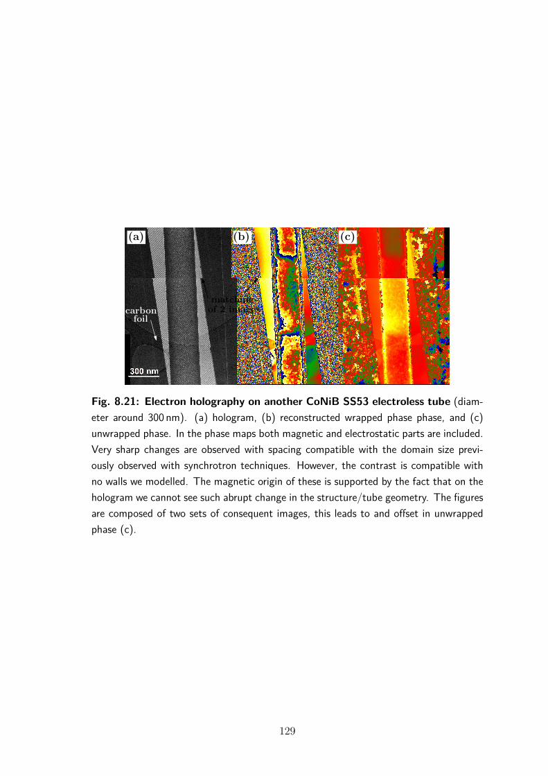
(a) (b) (c)
carbonfoil
matchingof 2 images
Fig. 8.21: Electron holography on another CoNiB SS53 electroless tube (diam-eter around 300 nm). (a) hologram, (b) reconstructed wrapped phase phase, and (c)unwrapped phase. In the phase maps both magnetic and electrostatic parts are included.Very sharp changes are observed with spacing compatible with the domain size previ-ously observed with synchrotron techniques. However, the contrast is compatible withno walls we modelled. The magnetic origin of these is supported by the fact that on thehologram we cannot see such abrupt change in the structure/tube geometry. The figuresare composed of two sets of consequent images, this leads to and offset in unwrappedphase (c).
129

We also applied external magnetic field before acquiring images. It had verylittle influence on the magnetic configuration as already observed with synchrotronXMCD.
To summarize this section: in aged (almost 1.5 years) CoNiB electroless tubeswe observed some axial component of magnetization in many parts of the tubes(indicating decrease of the azimuthal anisotropy strength) as well as some strangephase patterns which could be in some cases ascribed to domains wall. However,they do not look like simple Bloch walls, nor other common wall types.
MFM of aged tubes under vacuum
After some time we returned to magnetic force microscopy investigation of now aged(almost 1.5 years) SS53 CoNiB electroless tubes (initially with azimuthal domainsand Bloch walls as will be detailed in next chapter). As we now know that tubesare predominantly magnetized along the azimuthal direction forming multiple flux-closure domains, we expected only signal coming from the domain walls (azimuthaldomains create no stray field). As we were unable to detect any magnetic signal usingthe Ntegra microscope operated at ambient conditions, we switch to the Nanoscaninstrument operating under secondary vacuum (10−4 Pa) and thus better signal-to-noise ratio. First we tried high resolution MFM single pass non-contact imagingwith slow feedback-response. However, the large height of the structure made suchimaging impossible. Most of the signal was simply coming from the electrostaticinteraction or topography (van der Waals interaction). We tried imaging underdifferent tip/sample electrical bias, but not with fully compensated electrostaticcontribution.
We could have tried common two-pass tapping mode with the lift as on theNTegra microscope, but we wanted to avoid being too close to the sample as thetapping may damage the probe and the probe exchange is quite time consumingdue to the need to reach the low pressure in the chamber. Therefore, we decided toperform single pass constant height mode imaging with additional lift as suggestedby the microscope manufacturer and described in the methods section 5.2.2.
We have imaged two CoNiB electroless tubes (reminder: diameter and thusheight around 300 nm). Both are measured with the same probe coated with 10 nmCoCr. Due to sample ageing we can expect less sharp domains and more complexmagnetic structure than initially observed with XMCD-PEEM.
Fig. 8.22 shows a measurement of the first tube. The top image features EFMdone with -2 Hz setpoint and sample bias 1400 mV. It serves mainly for localizationof the structure. The bottom image (same area) is the constant height MFM withlift of 30 nm and compensated CPD (580 mV). As the potential is determined in the
130
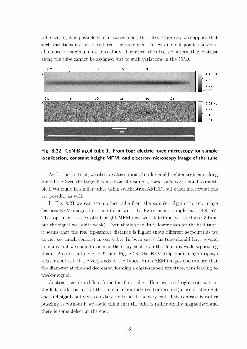
tube centre, it is possible that it varies along the tube. However, we suppose thatsuch variations are not very large – measurement in few different points showed adifference of maximum few tens of mV. Therefore, the observed alternating contrastalong the tube cannot be assigned just to such variations in the CPD.
Fig. 8.22: CoNiB aged tube 1. From top: electric force microscopy for samplelocalization, constant height MFM, and electron microscopy image of the tube
As for the contrast, we observe alternation of darker and brighter segments alongthe tube. Given the large distance from the sample, these could correspond to multi-ple DWs found in similar tubes using synchrotron XMCD, but other interpretationsare possible as well.
In Fig. 8.23 we can see another tube from the sample. Again the top imagefeatures EFM image, this time taken with -1.5 Hz setpoint, sample bias 1400 mV.The top image is a constant height MFM now with lift 0 nm (we tried also 30 nm,but the signal was quite weak). Even though the lift is lower than for the first tube,it seems that the real tip-sample distance is higher (note different setpoint) as wedo not see much contrast in our tube. In both cases the tube should have severaldomains and we should evidence the stray field from the domains walls separatingthem. Also in both Fig. 8.22 and Fig. 8.23, the EFM (top one) image displaysweaker contrast at the very ends of the tubes. From SEM images one can see thatthe diameter at the end decreases, forming a cigar-shaped structure, thus leading toweaker signal.
Contrast pattern differs from the first tube. Here we see bright contrast onthe left, dark contrast of the similar magnitude (vs background) close to the rightend and significantly weaker dark contrast at the very end. This contrast is ratherpuzzling as without it we could think that the tube is rather axially magnetized andthere is some defect at the end.
131

Fig. 8.23: CoNiB aged tube 2. From top: electric force microscopy for samplelocalization, constant height MFM, and electron microscopy image of the tube.
These are just preliminary measurements that could be further refined (+moretube measured). As we tried to be cautious, we know that we have a safety mar-gin as for the tip sample distance and we can go closer (e.g. setting lower = morenegative setpoint, and smaller lift – even negative) and benefit from increased sig-nal and spatial resolution. This could help us to assign the contrast to magneticconfiguration with help of other measurements (STXM, electron holography). Ascurrently we have MFM measurements of only 2 tubes, with very different patterns.Still showing that there seems to be some considerable change of the magnetic stateof the tubes through time.
Further, one may try also a so-called dual-PLL MFM, so called bimodal MFM [222,223]. In this non-contact technique the cantilever is driven at two frequencies at thesame time – primary and first overtone. The overtone is used for 𝑧-feedback andmonitors topography, whereas primary is more sensitive to long range magnetic in-teraction. In addition, it is possible to compensate the CPD non only based on onepoint of the sample, but by performing Kelvin force probe microscopy [184] we cando the compensation at every point of our image. However, both mentioned meth-ods increase the complexity of the experiment. Also to the best of our knowledge,the bimodal MFM was employed so far for topography features having height max70 nm and our tubes with 300 nm could be a considerable challenge. In the worstcase, one may try classical two pass tapping technique with the lift mode.
132
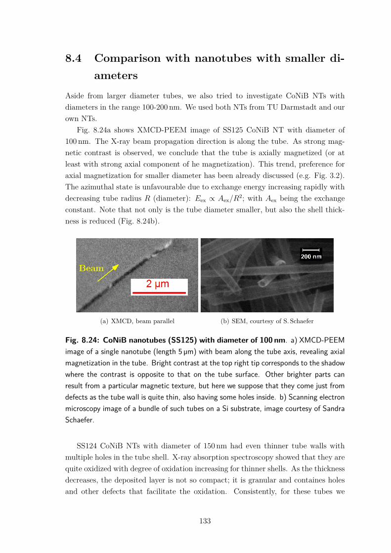
8.4 Comparison with nanotubes with smaller di-ameters
Aside from larger diameter tubes, we also tried to investigate CoNiB NTs withdiameters in the range 100-200 nm. We used both NTs from TU Darmstadt and ourown NTs.
Fig. 8.24a shows XMCD-PEEM image of SS125 CoNiB NT with diameter of100 nm. The X-ray beam propagation direction is along the tube. As strong mag-netic contrast is observed, we conclude that the tube is axially magnetized (or atleast with strong axial component of he magnetization). This trend, preference foraxial magnetization for smaller diameter has been already discussed (e.g. Fig. 3.2).The azimuthal state is unfavourable due to exchange energy increasing rapidly withdecreasing tube radius 𝑅 (diameter): 𝐸ex ∝ 𝐴ex/𝑅2; with 𝐴ex being the exchangeconstant. Note that not only is the tube diameter smaller, but also the shell thick-ness is reduced (Fig. 8.24b).
Beam
(a) XMCD, beam parallel (b) SEM, courtesy of S. Schaefer
Fig. 8.24: CoNiB nanotubes (SS125) with diameter of 100 nm. a) XMCD-PEEMimage of a single nanotube (length 5 µm) with beam along the tube axis, revealing axialmagnetization in the tube. Bright contrast at the top right tip corresponds to the shadowwhere the contrast is opposite to that on the tube surface. Other brighter parts canresult from a particular magnetic texture, but here we suppose that they come just fromdefects as the tube wall is quite thin, also having some holes inside. b) Scanning electronmicroscopy image of a bundle of such tubes on a Si substrate, image courtesy of SandraSchaefer.
SS124 CoNiB NTs with diameter of 150 nm had even thinner tube walls withmultiple holes in the tube shell. X-ray absorption spectroscopy showed that they arequite oxidized with degree of oxidation increasing for thinner shells. As the thicknessdecreases, the deposited layer is not so compact; it is granular and containes holesand other defects that facilitate the oxidation. Consistently, for these tubes we
133
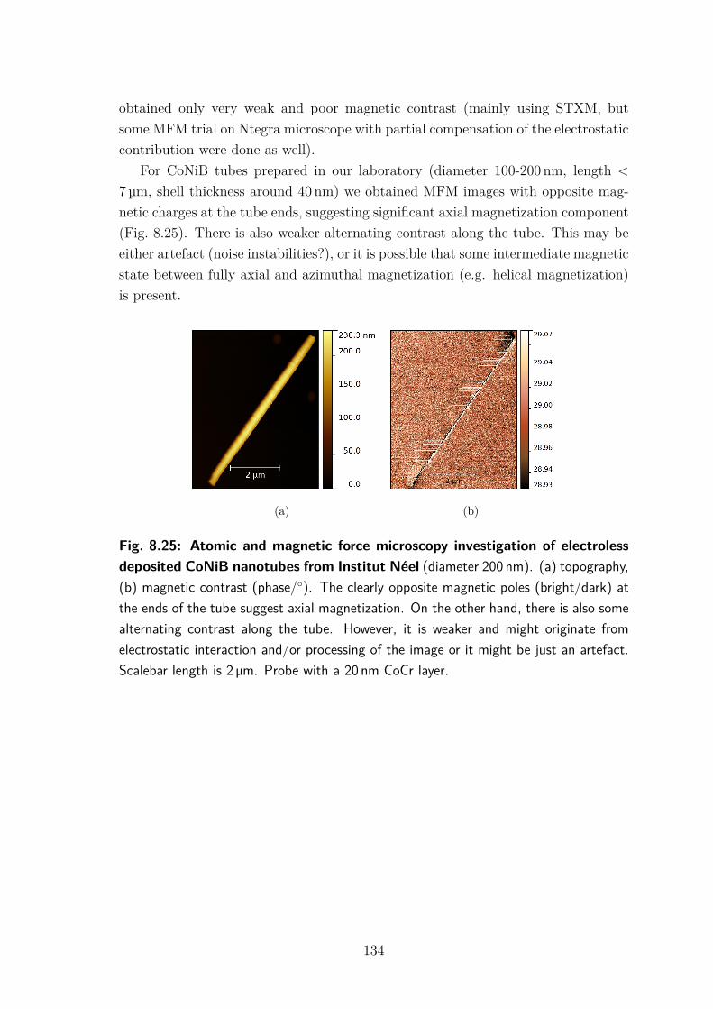
obtained only very weak and poor magnetic contrast (mainly using STXM, butsome MFM trial on Ntegra microscope with partial compensation of the electrostaticcontribution were done as well).
For CoNiB tubes prepared in our laboratory (diameter 100-200 nm, length <
7 µm, shell thickness around 40 nm) we obtained MFM images with opposite mag-netic charges at the tube ends, suggesting significant axial magnetization component(Fig. 8.25). There is also weaker alternating contrast along the tube. This may beeither artefact (noise instabilities?), or it is possible that some intermediate magneticstate between fully axial and azimuthal magnetization (e.g. helical magnetization)is present.
(a) (b)
Fig. 8.25: Atomic and magnetic force microscopy investigation of electrolessdeposited CoNiB nanotubes from Institut Néel (diameter 200 nm). (a) topography,(b) magnetic contrast (phase/∘). The clearly opposite magnetic poles (bright/dark) atthe ends of the tube suggest axial magnetization. On the other hand, there is also somealternating contrast along the tube. However, it is weaker and might originate fromelectrostatic interaction and/or processing of the image or it might be just an artefact.Scalebar length is 2 µm. Probe with a 20 nm CoCr layer.
134

9 DOMAIN WALLS IN TUBES WITH AZIMUT-HAL DOMAINS
As we have multiple magnetic domains in our CoNiB tubes (diameter of 300 nm; fordomains see Fig. 8.5), we will now focus on domain walls separating the azimuthaldomains. Information on the DW type and structure is one of the keys to determinethe mobility of a DW subjected to magnetic field and more importantly to spin-transfer torques [224]. We will start with an overview of possible DWs, we willcontinue with experimental observation. Further, we will provide more informationon the DWs.
9.1 Theoretical considerations
A simplified view of DWs between azimuthal domains can be obtained by imaginingthe tube unrolled into a flat strip (see Fig. 9.1). Two successive azimuthal domainswith opposite circulation turn into a thin film with in-plane magnetization and a180∘ DW parallel to magnetization in the domains. Note that the magnetic configu-ration at opposite ends of such unrolled film has to be the same (periodic boundarycondition) and that there are some difference highlighted in the next section. Aswas already discussed in section 3.2.2, for long nanotubes we may expect DWs ofBloch (radial magnetization) or Néel type (axial magnetization), named in analogyto thin films. Further, a cross-tie wall with axial magnetization components andvortex+anti-vortex pairs can be considered.
We could model all these walls by micromagnetic simulations in tubes with dif-ferent geometries (diameter and shell thickness) and imposed preferred azimuthaldirection for the magnetization. Examples of the resulting configurations follow:Bloch and Néel wall in Fig. 9.2 and Fig. 9.3, and cross-tie wall in Fig. 9.4. Asidefrom these some combinations of geometry and imposed anisotropy led to strangemagnetic configurations that could be analogues of asymmetric Néel and asymmetricBloch walls in thin films.
9.2 Bloch versus Néel walls in magnetic nanotubes
In thin films, the domain wall (DW) type, Bloch vs Néel, depends mainly on thefilm thickness. The transition is reported around 20-40 nm for 180∘ DWs andmagnetically-soft films. However, it can be affected by an additional magneticanisotropy, such as magnetocrystalline [66]. We found a similar trend in the mi-cromagnetic simulations of our nanotubes with azimuthal domains, where Néel-like
135

zz z
z z z
z
z
z
Neel
Bloch
Cross-tie
z z z
Wall
Wall
Wall
Fig. 9.1: Scheme of domain walls in nanotubes with azimuthal domains. Left:Scheme of idealized walls in unrolled tubes/thin film elements. Right: cross-sections ofa tube with two opposite azimuthal domains and the wall in the middle. The nanotubeaxis lies along 𝑧.
DWs are favoured for small tube wall thickness and Bloch-type DWs for larger ones.We expect the DW structure to be influenced by diameter as well. As in the sim-ulations we promote the azimuthal domains by defining the tube axis as a hardaxis (uniaxial effective anisotropy), Bloch walls are preferred for larger anisotropyconstants. A more systematic study of geometries with a different way of promotingthe azimuthal magnetization (azimuthal easy axis) could be done to build a phasediagram of the DWs.
Aside from modelling of small tubes (diameter 50 nm) we performed micromag-netic simulations [203] for tubes with diameter 120 nm, tube wall thickness 30 nmand length of 1000 nm. The end charges are removed in the calculation of the dipo-lar field, to mimick an infinitely-long structure. We suppose permalloy-like materialwith an effective uniaxial anisotropy with hard axis along the tube (making effec-tively azimuthal direction the easy axis) and anisotropy constants 30 kJ/m3 and100 kJ/m3, for which Néel and Bloch walls are obtained as a relaxed states, respec-tively. The simulation provides results similar to the ones for smaller tubes, onlythe extent of Bloch-like DWs with respect to the tube diameter is smaller (it mightbe also caused by the anisotropy values considered here). For these reasons andqualitative-only comparison, in the further discussion we will use tubes with thesmaller diameter, for the sake of clarity and saving the computation resources.
For a better visualization of the micromagnetic configuration of Bloch and NéelDWs, we display the tube outer surface as if unrolled (Fig. 9.3).
136
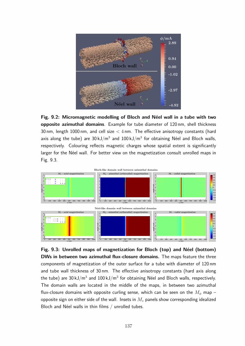
φ/mA
Bloch wall
Neel wall
2.89
0.94
-1.02
-2.97
-4.92
0.00
Fig. 9.2: Micromagnetic modelling of Bloch and Néel wall in a tube with twoopposite azimuthal domains. Example for tube diameter of 120 nm, shell thickness30 nm, length 1000 nm, and cell size < 4 nm. The effective anisotropy constants (hardaxis along the tube) are 30 kJ/m3 and 100 kJ/m3 for obtaining Néel and Bloch walls,respectively. Colouring reflects magnetic charges whose spatial extent is significantlylarger for the Néel wall. For better view on the magnetization consult unrolled maps inFig. 9.3.
Mz - axial magnetization
angle/ra
d
-3
-2
-1
0
1
2
3
4
-4500 600 700 800 900 10004003002001000z/nm
0
0.2
0.4
0.6
0.8
1.0
-0.2
-0.4
-0.6
-0.8
-1.0
Bloch-like domain wall between azimuthal domains
angle/ra
d
Mφ - azimuthal (orthoradial) magnetization
-3
-2
-1
0
1
2
3
4
-40 500 600 700 800 900 1000400300200100
z/nm
Mr - radial magnetization
angle/ra
d
-3
-2
-1
0
1
2
3
4
-40 500 600 700 800 900 1000400300200100
z/nm
Mz - axial magnetization
an
gle
/ra
d
-3
-2
-1
0
1
2
3
4
-4500 600 700 800 900 10004003002001000z/nm
Mφ - azimuthal (orthoradial) magnetization Mr - radial magnetization
an
gle
/ra
d
-3
-2
-1
0
1
2
3
4
-40
an
gle
/ra
d
-3
-2
-1
0
1
2
3
4
-40500 600 700 800 900 1000400300200100
z/nm500 600 700 800 900 1000400300200100z/nm
Neel-like domain wall between azimuthal domains
0
0.2
0.4
0.6
0.8
1.0
-0.2
-0.4
-0.6
-0.8
-1.0
Fig. 9.3: Unrolled maps of magnetization for Bloch (top) and Néel (bottom)DWs in between two azimuthal flux-closure domains. The maps feature the threecomponents of magnetization of the outer surface for a tube with diameter of 120 nmand tube wall thickness of 30 nm. The effective anisotropy constants (hard axis alongthe tube) are 30 kJ/m3 and 100 kJ/m3 for obtaining Néel and Bloch walls, respectively.The domain walls are located in the middle of the maps, in between two azimuthalflux-closure domains with opposite curling sense, which can be seen on the 𝑀𝜑 map –opposite sign on either side of the wall. Insets in 𝑀𝑧 panels show corresponding idealizedBloch and Néel walls in thin films / unrolled tubes.
137

Note that maps are very similar for the inner surface. The maps show the threecylindrical components of magnetization: 𝑀𝑧 (axial direction), 𝑀𝜑 (azimuthal di-rection), and 𝑀𝑟 (radial direction). Unlike for smaller diameters, the Bloch wallis associated with a weak (but non-negligible) bipolar axial component of magneti-zation, and the Néel wall with a weak bipolar radial component. These, which donot occur for flat thin films, result from the rolled geometry and the bipolar line ofcharge, which breaks the symmetry between the inner versus outer surface. Notethat in general Bloch walls are narrower than Néel walls, the latter giving rise todipolar field similar to walls between axially-magnetized domains. Tails indeed arisein the latter due to the dipolar line of charges of opposite sign found on either side ofthe wall (Fig. 9.3), implying a longitudinal dipolar field, while the radial distributionof charges in Bloch walls does not contribute to a longitudinal component of dipolarfield in the limit of thin-wall tubes.
Thus, even though the azimuthal domains produce no magnetic stray field, thisis not the case for the walls that separate them. Bloch walls with radial magneti-zation do generate some stray field. However, the field has a smaller spatial extentand decays faster (∝ 1/𝑟4) due to a quadrupolar nature of the magnetic chargescompared to the field from domain walls in between axial domains (e.g. in wires,tubes, strips) - magnetic dipoles (field ∝ 1/𝑟3), or even monopolar behaviour insome cases.
Note on cross-tie walls in magnetic nanotubes
In our simulations and discussion of domain wall types between azimuthal domainswe have also considered analogy of cross-tie walls from flat thin films. In Fig. 9.4 wemention an example of such wall in a small diameter permalloy-like tube (diameter50 nm, length 200 nm, shell thickness 10 nm, cell size 1 nm, OOMMF) with onevortex-antivortex pair. The azimuthal magnetization in domains is favoured bydefining varying easy axis along the tube perimeter with effective anisotropy constant50 kJ/m3. Larger number of pairs could be obtained for different anisotropy strengthand geometry (e.g. larger number possible for bigger diameter) – see also [93, 94].
9.3 Experimental observation and discussion
In order to determine the DW configuration in our CoNiB tubes we relied on XMCD-PEEM. We considered again the tubes with the X-ray beam both along and per-pendicular to their axis (e.g. Fig. 8.4) and compared experimental images with a
138

(a) view on antivortex
(b) view on vortex
Fig. 9.4: Micromagnetic simulation of a cross-tie wall in a nanotube with onevortex-antivortex pair. Coloured according to the axial (𝑧) magnetization.
numerical modelling based on micromagnetic simulations and XMCD-PEEM post-processing (see methods). No XMCD contrast is seen with the beam parallel to thetubes, from which we exclude Néel DWs (axial magnetization), also the presenceof the cross-tie wall is less likely. Therefore, DWs should be of the Bloch type.This is consistent with the images for the beam now perpendicular to the tubeaxis (Fig. 9.5).
Here, the domain boundary on the tube surface appears tilted with respect tothe tube axis both in the experiment (Fig. 9.5a) and for the simulation with Blochwall (Fig. 9.5b). While the tilt may be at first sight thought to result from a physicaltilt of the wall, it reflects that magnetization in the Bloch DW changes directionfrom parallel to antiparallel to the X-ray beam when going from the front to theback side of the tube surface. This behaviour can be fully reproduced with theXMCD-PEEM simulations without any physical tilt of the wall. Still we cannotrule out completely the possibility of a small physical tilt (e.g. 5∘) or other DWdistortions due to possible defects in the tube as these would not be manifested inthe images due to the limited spatial resolution. Note also that there is no suchtilt of the domain boundary in the shadow (for the beam perpendicular to thetube axis). Again, small (e.g. 5∘ physical tilts could be hard to distinguish due tolimited resolution (30-40 nm) and the fact that the shadow is elongated (approx. 3.6times the tube diameter due to the X-ray beam incidence angle). Larger physicaltilts would lead to changes in the images that are not observed in the experiment.
139

b) c)
z
x
y
z z z
Tube
Shadow
Beam
zz z
a)
Beam
Tube
Shadow
1µm
Fig. 9.5: Domain walls between flux-closure domains: experiment vs simula-tion. a) Experimental XMCD-PEEM with the beam perpendicular to the CoNiB tube(diameter around 300 nm, shell thickness 30 nm, length 30 µm). Five azimuthal domainsare featured; the red rectangle highlights an area with one domain wall. Simulation ofXMCD-PEEM contrast for b) Bloch and c) Néel walls. Schematic tube cross-sectionsbelow the simulations show the magnetization in domains and the domain wall (in themiddle of the tube) respectively. Note that in the experiment part of the shadow iscovered by the structure itself. The simulations are based on small-diameter tubes(50 nm, shell thickness 10 nm, cell size 2 nm) with imposed hard axis along the tube axisto favour the azimuthal magnetization (otherwise tube with such geometry would beaxially magnetized). The X-ray absorption coefficient is the one for 80% Co.
140

In addition, from the micromagnetic point of view (supported also by numericalmodelling) there is no clear reason for tilting the domain wall as this leads to apenalty in exchange energy and there is no other gain (e.g. in dipolar energy)even when considering multiple domain walls. This is also given by the form ofanisotropy considered here. Physically tilted (surface) domain boundaries have beenreported in amorphous microwires with helical anisotropy and axial magnetizationcomponent [225]. However, as no axial magnetization is detected in the presentedcase, such case is unlikely. On the other hand, the azimuthal anisotropy may becomeweaker for example upon sample ageing. This may result in tube sections with someaxial magnetization component and more complex magnetic configurations. Thiswe partially observed with STXM and electron holography for some oxidized tubes(aged for 1 year).
In the majority of cases, the tilt is in the same direction for all walls in a giventube. As the domains alternate, this means that the DW contrast at the tube frontand back alternates between successive DWs. Therefore, the radial magnetizationpoints alternatively inwards and outwards (alternating domain wall polarity). Thiscase is shown in a simulation in Fig. 9.6a, while Fig. 9.6b shows the case with DWshaving the same radial component. The former allows a better closure of the fluxand as a result is found to be of lower energy, which may explain its predominancein the experiments.
z
x
y
Tube
Shadow
z z z zBeam
Beam
a) b)
Fig. 9.6: Simulated XMCD-PEEM contrast for two Bloch DWs separatingthree azimuthal domains with alternating circulation. DWs with (a) opposite and(b) same radial components (polarity). Simulations are based on small tubes (diameter50 nm, tube wall thickness 10 nm) and only partially relaxed micromagnetic configura-tions (not necessarily stable for this geometry). Still it reflects well the main qualitativedifferences between the two configurations.
We performed also modelling of both XMCD-PEEM and electron holography
141
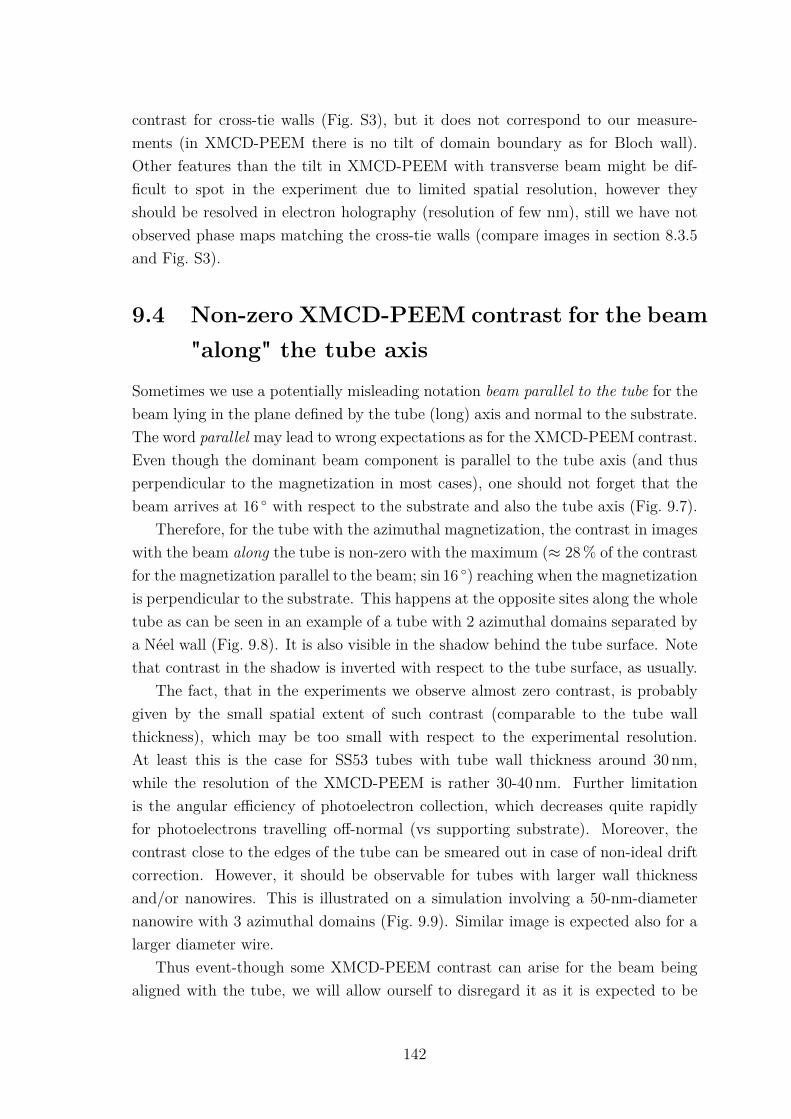
contrast for cross-tie walls (Fig. S3), but it does not correspond to our measure-ments (in XMCD-PEEM there is no tilt of domain boundary as for Bloch wall).Other features than the tilt in XMCD-PEEM with transverse beam might be dif-ficult to spot in the experiment due to limited spatial resolution, however theyshould be resolved in electron holography (resolution of few nm), still we have notobserved phase maps matching the cross-tie walls (compare images in section 8.3.5and Fig. S3).
9.4 Non-zero XMCD-PEEM contrast for the beam"along" the tube axis
Sometimes we use a potentially misleading notation beam parallel to the tube for thebeam lying in the plane defined by the tube (long) axis and normal to the substrate.The word parallel may lead to wrong expectations as for the XMCD-PEEM contrast.Even though the dominant beam component is parallel to the tube axis (and thusperpendicular to the magnetization in most cases), one should not forget that thebeam arrives at 16 ∘ with respect to the substrate and also the tube axis (Fig. 9.7).
Therefore, for the tube with the azimuthal magnetization, the contrast in imageswith the beam along the tube is non-zero with the maximum (≈ 28 % of the contrastfor the magnetization parallel to the beam; sin 16 ∘) reaching when the magnetizationis perpendicular to the substrate. This happens at the opposite sites along the wholetube as can be seen in an example of a tube with 2 azimuthal domains separated bya Néel wall (Fig. 9.8). It is also visible in the shadow behind the tube surface. Notethat contrast in the shadow is inverted with respect to the tube surface, as usually.
The fact, that in the experiments we observe almost zero contrast, is probablygiven by the small spatial extent of such contrast (comparable to the tube wallthickness), which may be too small with respect to the experimental resolution.At least this is the case for SS53 tubes with tube wall thickness around 30 nm,while the resolution of the XMCD-PEEM is rather 30-40 nm. Further limitationis the angular efficiency of photoelectron collection, which decreases quite rapidlyfor photoelectrons travelling off-normal (vs supporting substrate). Moreover, thecontrast close to the edges of the tube can be smeared out in case of non-ideal driftcorrection. However, it should be observable for tubes with larger wall thicknessand/or nanowires. This is illustrated on a simulation involving a 50-nm-diameternanowire with 3 azimuthal domains (Fig. 9.9). Similar image is expected also for alarger diameter wire.
Thus event-though some XMCD-PEEM contrast can arise for the beam beingaligned with the tube, we will allow ourself to disregard it as it is expected to be
142
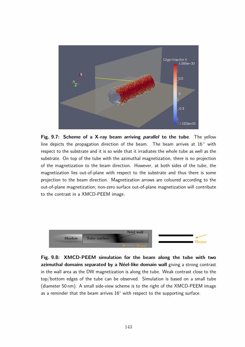
Fig. 9.7: Scheme of a X-ray beam arriving parallel to the tube. The yellowline depicts the propagation direction of the beam. The beam arrives at 16 ∘ withrespect to the substrate and it is so wide that it irradiates the whole tube as well as thesubstrate. On top of the tube with the azimuthal magnetization, there is no projectionof the magnetization to the beam direction. However, at both sides of the tube, themagnetization lies out-of-plane with respect to the substrate and thus there is someprojection to the beam direction. Magnetization arrows are coloured according to theout-of-plane magnetization; non-zero surface out-of-plane magnetization will contributeto the contrast in a XMCD-PEEM image.
Shadow
Neel wall
Beam
Tube surfaceBeam
Fig. 9.8: XMCD-PEEM simulation for the beam along the tube with twoazimuthal domains separated by a Néel-like domain wall giving a strong contrastin the wall area as the DW magnetization is along the tube. Weak contrast close to thetop/bottom edges of the tube can be observed. Simulation is based on a small tube(diameter 50 nm). A small side-view scheme is to the right of the XMCD-PEEM imageas a reminder that the beam arrives 16∘ with respect to the supporting surface.
143

Beam
Shadow Wire surface
(a) Simulated XMCD-PEEM
(b) Magnetic configuration
Fig. 9.9: Simulation of a solid nanowire with three azimuthal domains. (a)XMCD-PEEM simulation with beam along (16∘ with respect to the supporting surface)the wire axis. (b) Corresponding magnetic configuration, arrows are coloured accordingto a transverse normalized magnetization component (𝑀𝑦, -1..1). Note that this is acrude non-relaxed magnetic configuration. Therefore, it cannot describe properly whathappens at the domain boundaries.
weak and most likely cannot be resolved with current instrumentation.
144

Part IV
Results & DiscussionMultilayered nanotubes
So far we have been dealing with single-shell magnetic nanotubes.In view of obtaining enhanced magnetic properties and going to-wards devices based on nanotubes, we now study more complexgeometries. Namely we look at magnetic trilayers in tubular ge-ometry: two magnetic layers separated by a non-magnetic spacer.We provide both micromagnetic modelling and experiments onsuch core-shell structures.
145
Multilayered thin films with various magnetic and non-magnetic layers (spacers)are crucial in current spintronics. In curved, cylindrical geometry this implies coax-ial magnetic tubes with a spacer in between. To the best of our knowledge, thisgeometry has not been considered before in the literature. The first translation oftrilayered physics into tubular structures we aimed at was synthetic antiferromagnets(SAFs). Synthetic antiferromagnets and ferrimagnets are formed by two magneticlayers separated by a very thin (a few nanometres or even less) non-magnetic spacersuch as Ru. For certain spacer thickness, an antiparallel alignment of magnetizationin the two layers can be established through the RKKY interaction [50].
Here we focus on two axially-magnetized shells separated by a thicker spacer suchas 10 nm, because at the moment reliable fabrication of compact thinner layers is toochallenging in the tubular geometry, at least by (electro)chemistry that we employin the nanotube synthesis. Therefore, as a first step, our aim is to explore whetherwe can achieve antiparallel ordering just through magnetostatic interaction throughthe magnetic charges at tube ends of tubes with axial magnetization (or possiblydomain walls). Later one could investigate the micromagnetics and dynamics ofdomain walls in a such systems. In other words, we want to combine SAF withdomain walls in magnetic nanotubes which are predicted to propagate at very highspeed under both magnetic field and current without repeated transformations (andWalker breakdown).
In chapter 10 we focus on micromagnetic modelling of trilayered tubes with thespacer and in chapter 11 we show experimental realization and investigation of asimilar multilayer system in tubular geometry. However, with slightly different focusas for the physics.
146
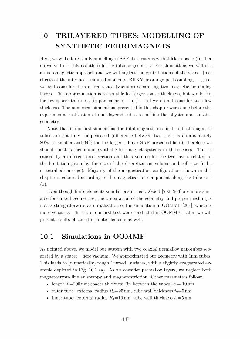
10 TRILAYERED TUBES: MODELLING OFSYNTHETIC FERRIMAGNETS
Here, we will address only modelling of SAF-like systems with thicker spacer (furtheron we will use this notation) in the tubular geometry. For simulations we will usea micromagnetic approach and we will neglect the contributions of the spacer (likeeffects at the interfaces, induced moments, RKKY or orange-peel coupling, . . . ), i.e.we will consider it as a free space (vacuum) separating two magnetic permalloylayers. This approximation is reasonable for larger spacer thickness, but would failfor low spacer thickness (in particular < 1 nm) – still we do not consider such lowthickness. The numerical simulations presented in this chapter were done before theexperimental realization of multilayered tubes to outline the physics and suitablegeometry.
Note, that in our first simulations the total magnetic moments of both magnetictubes are not fully compensated (difference between two shells is approximately80% for smaller and 34% for the larger tubular SAF presented here), therefore weshould speak rather about synthetic ferrimagnet systems in these cases. This iscaused by a different cross-section and thus volume for the two layers related tothe limitation given by the size of the discretization volume and cell size (cubeor tetrahedron edge). Majority of the magnetization configurations shown in thischapter is coloured according to the magnetization component along the tube axis(𝑧).
Even though finite elements simulations in FeeLLGood [202, 203] are more suit-able for curved geometries, the preparation of the geometry and proper meshing isnot as straightforward as initialization of the simulation in OOMMF [201], which ismore versatile. Therefore, our first test were conducted in OOMMF. Later, we willpresent results obtained in finite elements as well.
10.1 Simulations in OOMMF
As pointed above, we model our system with two coaxial permalloy nanotubes sep-arated by a spacer – here vacuum. We approximated our geometry with 1nm cubes.This leads to (numerically) rough "curved" surfaces, with a slightly exaggerated ex-ample depicted in Fig. 10.1 (a). As we consider permalloy layers, we neglect bothmagnetocrystalline anisotropy and magnetostriction. Other parameters follow:
• length 𝐿=200 nm; spacer thickness (in between the tubes) 𝑠 = 10 nm• outer tube: external radius 𝑅2=25 nm, tube wall thickness 𝑡2=5 nm• inner tube: external radius 𝑅1=10 nm, tube wall thickness 𝑡1=5 nm
147

• cell size 1 nm, damping 𝛼 = 0.1• exchange stiffness 𝐴 = 13 pJ/m, spontaneous magnetization 𝑀s = 860 kA/mWe started the simulation with a random magnetization direction in each cell.
When following the evolution of the system, first, magnetization was aligned alongthe common axis for the outer tube, followed by the inner tube. However, twodomains separated by a transverse wall were formed in the inner tube [consultFig. 10.1 (b)]. A similar evolution was observed also for a similar geometry mod-elled in finite elements (see below). Later on, the domain wall moves slightly towardsthe end of the structure with the parallel magnetization in both shells (left end inFig. 10.1b). Therefore, the antiparallely-aligned part (lower energy) extends and weexpect the wall to be annihilated, even though this has not happened so far duringseveral tens of thousands of steps. Note slight curling at the ends for the outer tube;we see only slight tilting of the magnetization at the ends for the smaller tube asthe curling is not favoured due to a large exchange energy penalty for such tiny tubediameter. Both these features seems to be consistent with the phase diagram forsingle-shell NTs: geometry of the outer tube lies in the mixed state part of the dia-gram (but close to the uniform state), whereas the inner tube would be completelyuniform (F) state (see Fig. 3.2).
(a) example of coaxial tubes’ geometry (b) SAF with a domain wall
Fig. 10.1: Tubular SAF in OOMMF (outer diameter 50 nm, shell thickness 5 nm,cell size 1 nm). (a) example of the geometry (coaxial tubes): the representation ofcurved surfaces with cubes is far from ideal. Note that the depicted example does notreflect exactly the geometry used in the simulations as 5 instead of 3-4 cells (shownhere) were used for the tube wall. The (over)simplification comes from the visualizationin ParaView. (b) Simulated magnetization (not completely relaxed) in the SAF with atransverse domain wall inside the inner tube. Only one half of the structure is shown, inorder to have a better view on the magnetization in both tubes.
148
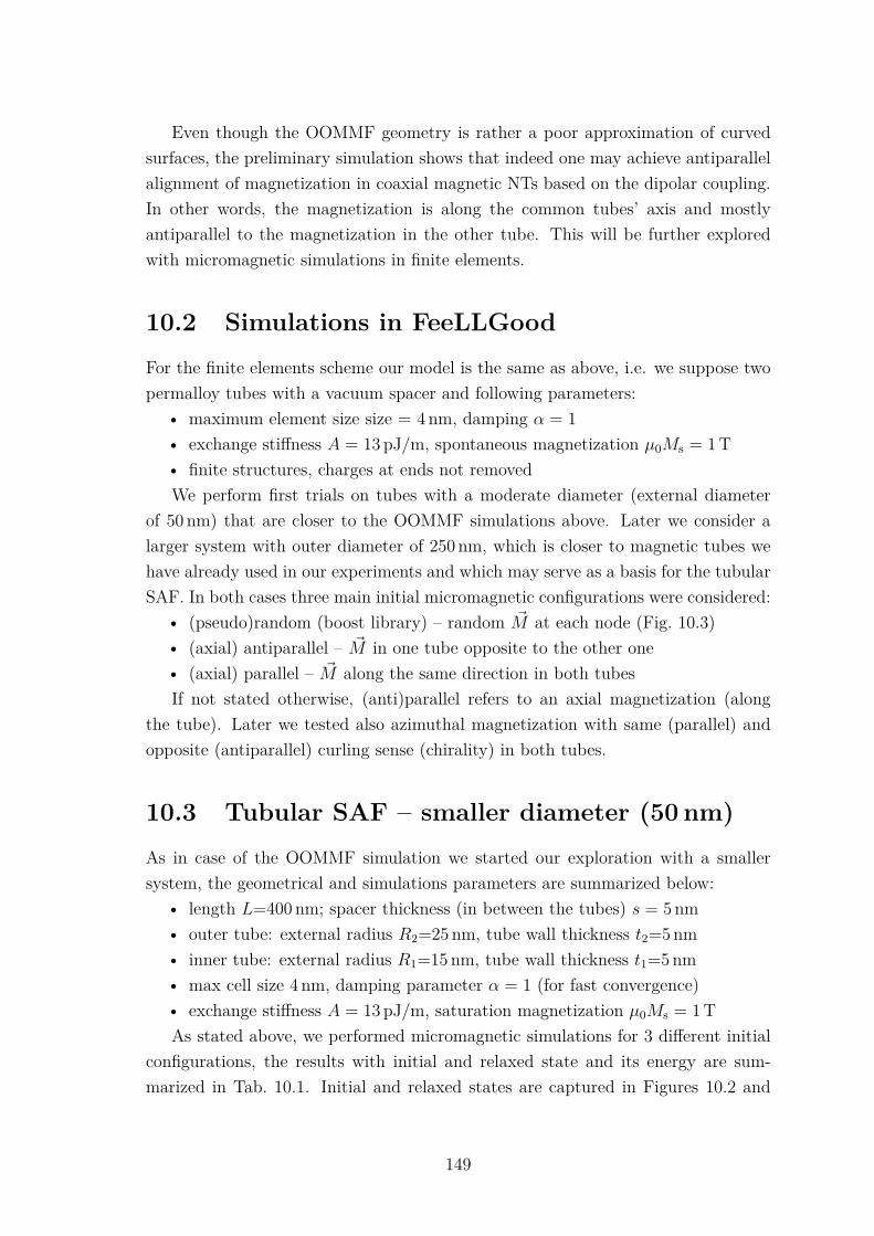
Even though the OOMMF geometry is rather a poor approximation of curvedsurfaces, the preliminary simulation shows that indeed one may achieve antiparallelalignment of magnetization in coaxial magnetic NTs based on the dipolar coupling.In other words, the magnetization is along the common tubes’ axis and mostlyantiparallel to the magnetization in the other tube. This will be further exploredwith micromagnetic simulations in finite elements.
10.2 Simulations in FeeLLGood
For the finite elements scheme our model is the same as above, i.e. we suppose twopermalloy tubes with a vacuum spacer and following parameters:
• maximum element size size = 4 nm, damping 𝛼 = 1• exchange stiffness 𝐴 = 13 pJ/m, spontaneous magnetization 𝜇0𝑀s = 1 T• finite structures, charges at ends not removedWe perform first trials on tubes with a moderate diameter (external diameter
of 50 nm) that are closer to the OOMMF simulations above. Later we consider alarger system with outer diameter of 250 nm, which is closer to magnetic tubes wehave already used in our experiments and which may serve as a basis for the tubularSAF. In both cases three main initial micromagnetic configurations were considered:
• (pseudo)random (boost library) – random �� at each node (Fig. 10.3)• (axial) antiparallel – �� in one tube opposite to the other one• (axial) parallel – �� along the same direction in both tubesIf not stated otherwise, (anti)parallel refers to an axial magnetization (along
the tube). Later we tested also azimuthal magnetization with same (parallel) andopposite (antiparallel) curling sense (chirality) in both tubes.
10.3 Tubular SAF – smaller diameter (50 nm)
As in case of the OOMMF simulation we started our exploration with a smallersystem, the geometrical and simulations parameters are summarized below:
• length 𝐿=400 nm; spacer thickness (in between the tubes) 𝑠 = 5 nm• outer tube: external radius 𝑅2=25 nm, tube wall thickness 𝑡2=5 nm• inner tube: external radius 𝑅1=15 nm, tube wall thickness 𝑡1=5 nm• max cell size 4 nm, damping parameter 𝛼 = 1 (for fast convergence)• exchange stiffness 𝐴 = 13 pJ/m, saturation magnetization 𝜇0𝑀s = 1 TAs stated above, we performed micromagnetic simulations for 3 different initial
configurations, the results with initial and relaxed state and its energy are sum-marized in Tab. 10.1. Initial and relaxed states are captured in Figures 10.2 and
149

(a) Magnetic scalar potential in amps (b) Magnetization vector
Fig. 10.2: Illustration of a random initial micromagnetic configuration on SAFmultilayered tubes. Magnetization at each node is assigned using a pseudorandomnumber generator. (a) scalar magnetic (pseudo)potential (in amps), (b) magnetizationdepicted with normalized vectors pointing randomly in all directions.
10.3 (initial �� : random), 10.4 (initial �� : antiparallel) and 10.5 (initial �� : par-allel). From now on, only one half of the structure (cut through the common tubeaxis) will be displayed in order to have a clear picture of magnetization in bothtubes.
Tab. 10.1: Summary of simulations of tubular SAF – smaller system in FeeLL-Good: length 𝐿=400 nm, outer and inner tube diameter 𝐷2=50 nm and 𝐷1=30 nmrespectively, tube wall thickness and spacing 𝑡2 = 𝑡1 = 𝑠 = 5 nm.
Initial state Relaxed state Relaxed energy Referencerandom antiparallel 4.13·10−18 J Fig. 10.3
antiparallel antiparallel 4.13·10−18 J Fig. 10.4parallel parallel 8.84·10−18 J Fig. 10.5
The initially random magnetization evolves in a very similar way to the OOMMFcase described above, only a vortex-like wall (Fig. 10.3) is present in the inner tube(diameter of 30 nmm instead of 20 nm for the OOMMF simulation).
Both random and antiparallel initial configuration resulted in the antiparallelaxial magnetization in the two tubes having basically the same energy. The onlydifference is the end curling which can have either same or opposite sense at bothtube ends. Recall that in a single-shell tube there should not be any preference forthe curling sense at the end [79]. Note that the end curling is clearly observed onlyfor the outer tube with larger diameter; it looks like there is only inward or outwardtilting of the magnetization for the inner tube (diameter 30 nm) – in Landeros phasediagram (Fig. 3.2) such tube would be in the uniform axial state.
150
(a) Slice of intermediate state – vortex-like wall
(b) Relaxed – magnetic scalar potential/A (c) Relaxed state – magnetization
Fig. 10.3: Small tubular SAF system (outer diameter 50 nm): random initialmagnetization (depicted in Fig. 10.2). (a) Slice of the tubes in an intermediate statewith a vortex-like wall in the inner shell; the outer one is uniformly magnetized. Afterrelaxation, antiparallel state is established: (b) scalar magnetic potential (reflects alsomagnetic charges – at ends) and (c) magnetization.
151

(a) Initial state
(b) Relaxed state
Fig. 10.4: Small tubular SAF system (outer diameter 50 nm): antiparallel initialconfiguration.
The structure with initially parallel alignment of the magnetization kept thisarrangement, only curling/tilt of magnetization developed at the ends as discussedabove. However, the energy of the relaxed state is more than two times higher thanfor the antiparallel alignment. Similar ratio of energies is found also in flat thinfilms [226]. The antiparallel state is preferred, while the parallel one may exist as ametastable state.
152
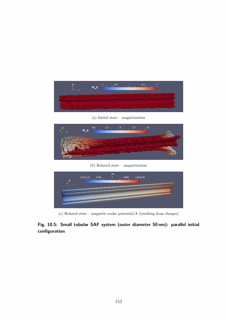
(a) Initial state – magnetization
(b) Relaxed state – magnetization
(c) Relaxed state – magnetic scalar potential/A (resulting from charges)
Fig. 10.5: Small tubular SAF system (outer diameter 50 nm): parallel initialconfiguration.
153

10.3.1 Simulated contrast for electron holography
We performed also crude simulations of expected magnetic phase maps for electronholography on tubular SAF. We used relaxed tubular SAF configuration discussedabove – parallel [Fig. 10.5(b)] and antiparallel [Fig. 10.4(b)] magnetization in the twonanotubes. Fig. 10.6 shows that a clear difference between parallel and antiparallelstates can be observed in the electron holography. In other words it should bepossible to distinguish the two states using electron holography. Note that in ourcase [Fig. 10.6 (a)] the two tubes do not have the same cross-section and thusthey do not compensate fully each other due in terms of magnetic moment. The fullcompensation would lead to the same potential and thus phase outside the structure– i.e. same level both on the left and right of Fig. 10.6a-b.
10.4 Tubular SAF – larger diameter (250 nm)
The simulations on the smaller system (both OOMMF and FeeLLGood) showedthat the magnetization in two coaxial tubes with a spacer can be in the antiparallelstate, thus forming a synthetic ferrimagnet. Now we will explore larger systemsconsisting of tubes with larger diameter (250 nm), which is closer to our electrolesstubes (SS53 NiCoB tubes) used in the synchrotron experiments. The geometry andsimulation parameters are given below:
• length 𝐿=2000 nm; spacer thickness (in between the tubes) 𝑠 = 15 nm• outer tube: external radius 𝑅2=125 nm, tube wall thickness 𝑡2=15 nm• inner tube: external radius 𝑅1=95 nm, tube wall thickness 𝑡1=15 nm• max cell size 4 nm, damping parameter 𝛼 = 1 (for fast convergence)• exchange stiffness 𝐴 = 13 pJ/m, spontaneous magnetization 𝜇0𝑀s = 1 TAside from random and axial (anti)parallel initial configuration we also simulated
azimuthal magnetization (curling everywhere) with either same or opposite sense inthe two coaxial tubes. The results are gathered in Tab. 10.2.
As in the case of smaller tubes, the random and antiparallel initial configurationevolved to antiparallel alignment, now with the end curling present in both tubes.Note that again the sense of the end curling varies, it can be either the same at bothends or the opposite [Fig. 10.7 (a)-(b)].
Fig. 10.8 shows how the magnetization looks like when we consider only the outershell (diameter of 250 nm). The curling extends almost along the whole length ofthe tube (2 microns), therefore one may argue if this is an axially magnetized tubewith extended end curling or azimuthally magnetized tube with a Néel wall . . . Theextend of both end curling seems to be similar to models presented by Wyss etal. [79] (maybe our is slightly larger). Note that in our NiFeB tubes the end curling
154
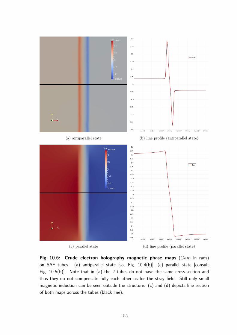
(a) antiparallel state (b) line profile (antiparallel state)
(c) parallel state (d) line profile (parallel state)
Fig. 10.6: Crude electron holography magnetic phase maps (𝐺𝑎𝑚 in rads)on SAF tubes. (a) antiparallel state [see Fig. 10.4(b)], (c) parallel state [consultFig. 10.5(b)]. Note that in (a) the 2 tubes do not have the same cross-section andthus they do not compensate fully each other as for the stray field. Still only smallmagnetic induction can be seen outside the structure. (c) and (d) depicts line sectionof both maps across the tubes (black line).
155
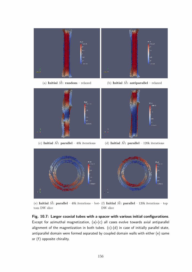
(a) Initial �� : random – relaxed (b) Initial �� : antiparallel – relaxed
(c) Initial �� : parallel – 40k iterations (d) Initial �� : parallel – 120k iterations
(e) Initial �� : parallel – 40k iterations – bot-tom DW slice
(f) Initial �� : parallel – 120k iterations – topDW slice
Fig. 10.7: Larger coaxial tubes with a spacer with various initial configurations.Except for azimuthal magnetization, (a)-(c) all cases evolve towards axial antiparallelalignment of the magnetization in both tubes. (c)-(d) in case of initially parallel state,antiparallel domain were formed separated by coupled domain walls with either (e) sameor (f) opposite chirality.
156

Tab. 10.2: Summary of simulations of tubular SAF – larger system in FeeLL-Good: length 𝐿=2000 nm, outer and inner tube diameter 𝐷2=250 nm and 𝐷1=190 nmrespectively, tube wall thickness and spacing 𝑡2 = 𝑡1 = 𝑠 = 15 nm.
Initial state Relaxed state Relaxed energyazimuthal – same chirality azimuthal – same chirality 4.90 · 10−17 J
azimuthal – opposite chirality azimuthal – opposite chirality 4.90 · 10−17 Jrandom axial antiparallel 2.00 · 10−17 J
axial antiparallel axial antiparallel 2.00 · 10−17 Jaxial parallel axial antiparallel domains† ◇
† After few thousands iterations 3 antiparallel domains were established. Muchlater one moved towards the end of the structure and annihilated, the other oneremains even after 160 k iterations. The total micromagnetic energy(dipolar+exchange) is higher than mono-domain antiparallel state, as expected.◇ Energy around 3.61 · 10−17 J after 137 · 103 iterations (=several months).
was mostly not present. Still it is clear that SAF geometry promotes the axialmagnetization even for large diameters and short tubes [compare with Fig. 10.7(a)-(b)].
The simulation with initially parallel alignment of the magnetization is moreinteresting for large tubes (but there is also the effect of larger spacer). Insteadof staying parallel as for small tubes, 3 antiparallel domains separated by coupledvortex-like walls were established [Fig. 10.7(c)]. The domain walls are present inboth tubes at the same location and they have either same [Fig. 10.7(e)] or oppositechirality [Fig. 10.7(f)]. Later the domain walls with the same chirality moved tothe end of the structure and annihilated. The other couple (opposite chirality) ofdomain walls moved only slightly and still persist [Fig. 10.7(d)] even after almost140 thousands iterations and there is almost no change in the magnetization (closeto a convergence condition).
As for the azimuthal magnetization (no anisotropy introduced), both simulationsended quickly keeping the initial configuration. Independent of chirality, the totalmagnetic energy is the same and it is significantly larger than axial antiparallelconfiguration that is the most energetically favourable. Still it could be a metastablestate – to be further investigated. Azimuthal magnetization in both tubes, eitherwith same or opposite chirality, looks like domain wall slices in Fig. 10.7 (e) and (f),just this state is present along the whole structure.
157
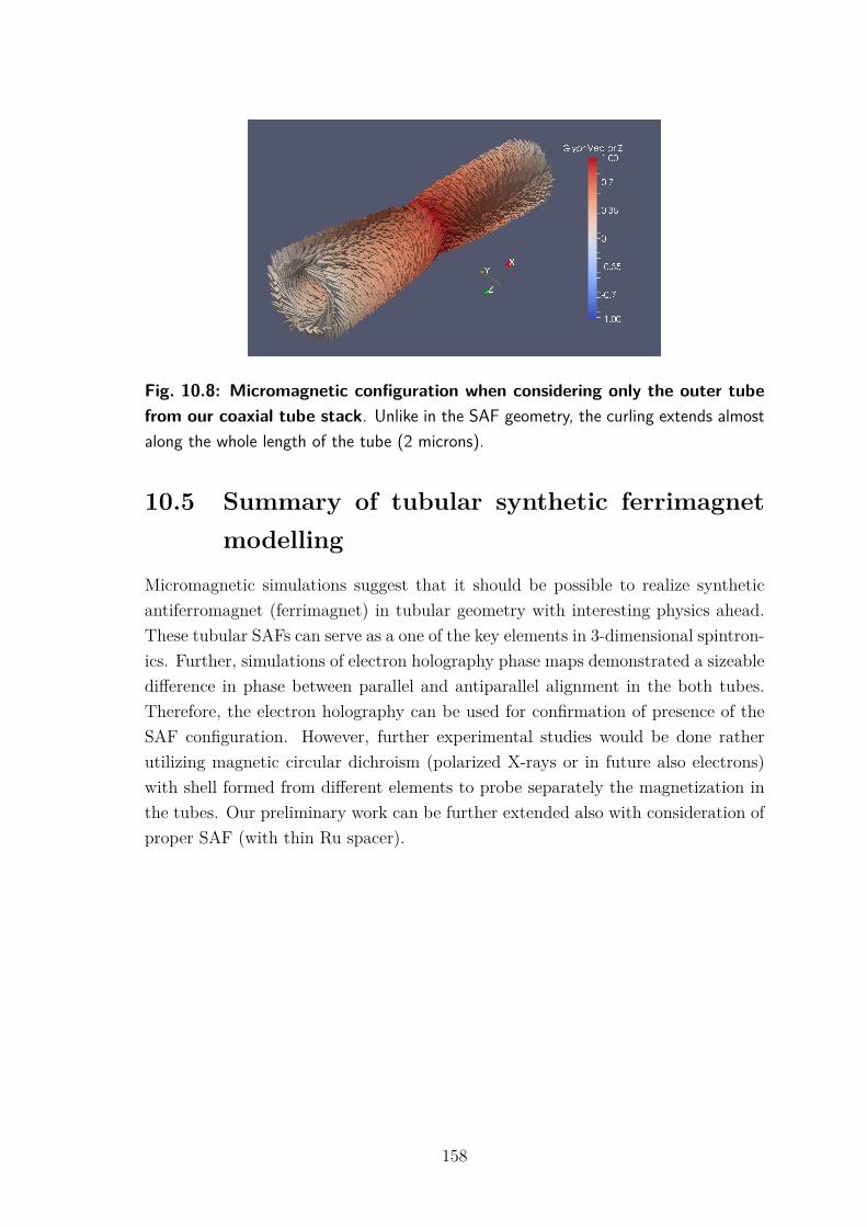
Fig. 10.8: Micromagnetic configuration when considering only the outer tubefrom our coaxial tube stack. Unlike in the SAF geometry, the curling extends almostalong the whole length of the tube (2 microns).
10.5 Summary of tubular synthetic ferrimagnetmodelling
Micromagnetic simulations suggest that it should be possible to realize syntheticantiferromagnet (ferrimagnet) in tubular geometry with interesting physics ahead.These tubular SAFs can serve as a one of the key elements in 3-dimensional spintron-ics. Further, simulations of electron holography phase maps demonstrated a sizeabledifference in phase between parallel and antiparallel alignment in the both tubes.Therefore, the electron holography can be used for confirmation of presence of theSAF configuration. However, further experimental studies would be done ratherutilizing magnetic circular dichroism (polarized X-rays or in future also electrons)with shell formed from different elements to probe separately the magnetization inthe tubes. Our preliminary work can be further extended also with consideration ofproper SAF (with thin Ru spacer).
158

11 TRILAYERED TUBES: EXPERIMENTS
In the previous chapter we probed with micromagnetic simulations the possibility ofobtaining synthetic ferrimagnets in tubular geometry through dipolar coupling andthicker non-magnetic spacer (e.g. 10 nm). Here we show experimental realizationof such trilayers. In the following sections we provide structural, chemical andmainly magnetic investigation of the multilayered tubes. Note that the focus as forphysics is different as one of our magnetic layers (CoNiB) displays similar azimuthalanisotropy to single-layered tubes discussed in chapter 8. Therefore, we will focuson obtaining (exchange) decoupled magnetic layers. Still we will also briefly discusshow one could obtain the tubular SAF.
11.1 Structural and chemical analysis
In our case, we used electroless plating (see section 4.4.3) to prepare the multilayeredsystem such as in Fig. 11.1. We used different elemental composition of the layers, sothat we could disentangle the magnetization in each magnetic layer by utilizing theelement specificity of the synchrotron X-ray magnetic microscopy (XMCD-PEEM).
NiFeB
SnOx
CoNiB
Fig. 11.1: Multilayered tube with a non-magnetic (oxide) spacer. Experimentalrealization (left) – transmission electron microscopy of a tube segment (electrons arriveperpendicular to the tube axis). The oxide spacer appears as a brighter line in the tubewall. Scheme to the right highlights the different layers of the tube.
At TU Darmstadt, S. Schaefer prepared several samples with different tubelengths, different non-magnetic spacers and their (chemical) modification for thesubsequent deposition of the inner magnetic layer. Two main spacers were tested –metallic (Pd) and insulating (SnO𝑥), yielding multilayered tubular stacks NiFeB/Pd/-CoNiB (sample SS147) and NiFeB/SnO𝑥/CoNiB (sample SS148).
Fig. 11.2 displays electron microscopy and chemical mapping of a set of twomultilayered tubes from the SS148 sample, dispersed on a TEM grid. The left tubecontains all three layers (NiFeB, SnO𝑥, and CoNiB) whereas the other one lacks the
159

inner CoNiB layer. Transmission electron microscopy shows that proper multilay-ered tubes are thick, with the total tube wall thickness around 90 nm. The SnO𝑥
spacer is represented by a bright line in the otherwise dark tube wall (Fig. 11.2a,left tube). The measured thickness of the layers from the TEM images (highermagnification) is as follows (deviation up to ±5 nm, except SnO𝑥 – rather largerthickness):
• outer shell: NiFeB approx 30 nm• spacer: SnOx approx 10 nm (may be underestimated see below)• inner shell: CoNiB approx 50 nmDue to the large thickness of the metallic layers, the SnOx (bright line) may
be underestimated; up to 20 nm thickness is expected from typical deposition rates(1 nm/h) for SnO𝑥 using the chemical bath deposition. As for the chemical mappingwith EDX, we can clearly see the presence of outer NiFeB (Fe) for both tubes; theinner CoNiB (Co) is only in the left tube. Unfortunately, we cannot see a well-localized spacer: Sn appears everywhere as it is also used for modification of thetube surface after deposition of each layer. Delocalized Sn presence is also causedby a large interaction volume (for 20 keV primary beam energy). Spacer from adifferent material would be more easy to detect, e.g. TiO2 that can be prepared invery similar way as SnO𝑥 [170].
Regarding the SS147 sample, no clear sign of Pd was detected with EDX, indi-cating that it may have been replaced during the deposition of the inner layer thatwas in some cases thicker than expected. Sometimes particles (most likely Sn) canbe seen inside the tubes. In several other tubes, the Pd spacer turned out to beinhomogeneous or completely missing. Therefore, in order to get a metallic spacer,different metal should be selected, such as copper. Alternatively, one can use adifferent fabrication technique, such as ALD that enables also deposition of puremetals [133].
Better results were obtained for the SnO𝑥, but even here significant portion oftubes was without the inner CoNiB core. This is caused mainly by blocked poreextremities as the membrane is polished after each deposition step. This may leadto obstruction of the pore openings. Only 2 out of 6 series of samples had signifi-cant amount of tubes with the inner CoNiB layer and only one sample had tubeswith both magnetic layers separated by the continuous spacer (SS148). The yieldof multilayered tubes could be significantly increased when using porous aluminatemplates. Here the excessive growth can be removed by ion beam etching insteadof the mechanical polishing. Ion etching could not be used in our case as polycar-bonate membranes are slightly burnt during the process (at least in our machine).In addition, ion etching can be performed just after the activation of the aluminamembrane with Pd seeds – this would remove the catalysts and thus prevent the
160
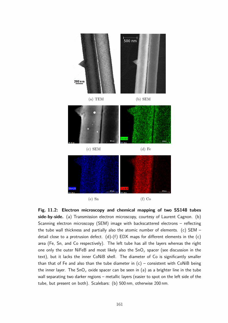
(a) TEM (b) SEM
(c) SEM (d) Fe
(e) Sn (f) Co
Fig. 11.2: Electron microscopy and chemical mapping of two SS148 tubesside-by-side. (a) Transmission electron microscopy, courtesy of Laurent Cagnon. (b)Scanning electron microscopy (SEM) image with backscattered electrons – reflectingthe tube wall thickness and partially also the atomic number of elements. (c) SEM –detail close to a protrusion defect. (d)-(f) EDX maps for different elements in the (c)area (Fe, Sn, and Co respectively). The left tube has all the layers whereas the rightone only the outer NiFeB and most likely also the SnO𝑥 spacer (see discussion in thetext), but it lacks the inner CoNiB shell. The diameter of Co is significantly smallerthan that of Fe and also than the tube diameter in (c) – consistent with CoNiB beingthe inner layer. The SnO𝑥 oxide spacer can be seen in (a) as a brighter line in the tubewall separating two darker regions – metallic layers (easier to spot on the left side of thetube, but present on both). Scalebars: (b) 500 nm, otherwise 200 nm.
161
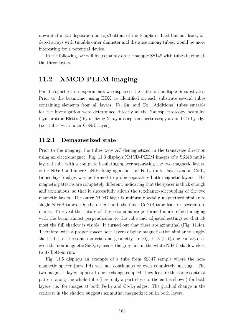
unwanted metal deposition on top/bottom of the template. Last but not least, or-dered arrays with tunable outer diameter and distance among tubes, would be moreinteresting for a potential device.
In the following, we will focus mainly on the sample SS148 with tubes having allthe three layers.
11.2 XMCD-PEEM imaging
For the synchrotron experiments we dispersed the tubes on multiple Si substrates.Prior to the beamtime, using EDX we identified on each substrate several tubescontaining elements from all layers: Fe, Sn, and Co. Additional tubes suitablefor the investigation were determined directly at the Nanospectroscopy beamline(synchrotron Elettra) by utilizing X-ray absorption spectroscopy around Co-L3 edge(i.e. tubes with inner CoNiB layer).
11.2.1 Demagnetized state
Prior to the imaging, the tubes were AC demagnetized in the transverse directionusing an electromagnet. Fig. 11.3 displays XMCD-PEEM images of a SS148 multi-layered tube with a complete insulating spacer separating the two magnetic layers,outer NiFeB and inner CoNiB. Imaging at both at Fe-L3 (outer layer) and at Co-L3
(inner layer) edges was performed to probe separately both magnetic layers. Themagnetic patterns are completely different, indicating that the spacer is thick enoughand continuous, so that it successfully allows the (exchange-)decoupling of the twomagnetic layers. The outer NiFeB layer is uniformly axially magnetized similar tosingle NiFeB tubes. On the other hand, the inner CoNiB tube features several do-mains. To reveal the nature of these domains we performed more refined imagingwith the beam almost perpendicular to the tube and adjusted settings so that al-most the full shadow is visible. It turned out that these are azimuthal (Fig. 11.4c).Therefore, with a proper spacer both layers display magnetization similar to single-shell tubes of the same material and geometry. In Fig. 11.3 (left) one can also seeeven the non-magnetic SnO𝑥 spacer – the grey line in the white NiFeB shadow closeto its bottom rim.
Fig. 11.5 displays an example of a tube from SS147 sample where the non-magnetic spacer (now Pd) was not continuous or even completely missing. Thetwo magnetic layers appear to be exchange-coupled: they feature the same contrastpattern along the whole tube (here only a part close to the end is shown) for bothlayers, i.e. for images at both Fe-L3 and Co-L3 edges. The gradual change in thecontrast in the shadow suggests azimuthal magnetization in both layers.
162

Beam
Fig. 11.3: NiFeB/SnO𝑥/CoNiB – decoupled magnetic layers (SS148 sample).In both images, shadow area at given absorption edge is highlighted with a dashed line.Here, the extent of the shadow, reflects the tube diameter. Thus, it is smaller at Coedge, as CoNiB is the inner layer (smaller diameter). The information from the tubesurface is weak due to the imaging conditions being optimized for the shadow and alsoin case of the inner layer no surface magnetic signal is expected. The outer NiFeB layeris uniformly magnetized along the tube axis (uniform transverse magnetization is highlyunlikely without external magnetic field). Note also the grey line in the white shadowclose to its bottom rim – this is the non-magnetic SnO𝑥 spacer. On the other hand,the inner CoNiB layer (smaller extent of the shadow) displays a completely differentmagnetization pattern with multiple domains. These are azimuthal as in a single CoNiBtube case (with similar geometry) as can be seen in Fig. 11.4c.
Beam
Tube
Shadow
Scatteringfringes
(a) XPEEM Fe-L3 (b) XMCD-PEEM Fe-L3 (c) XMCD-PEEM Co-L3
Fig. 11.4: Images of a SS148 multilayered tube (NiFeB/SnO𝑥/CoNiB). (a)PEEM image @ Fe-L3showing the tubular character. (b) XMCD-PEEM @ Fe-L3 withuniform contrast and magnetization, and (c) XMCD-PEEM @ Co-L3 with a clear contrastchange in the shadow indicating presence of azimuthal domains. Microscope settingsare adjusted for better collection of photoelectrons from the shadow (substrate surface).The defect at the tube end (top) is caused by the mechanical polishing of the membranewith tubes which may lead to tube opening being blocked, filled with both magnetic andnon-magnetic particles. The presence of this defect does not disturb the magnetizationand decoupling of both layers in other parts of the tube.
163

Beam
Fig. 11.5: NiFeB/Pd(incomplete)/CoNiB – coupled magnetic layers (SS147sample). XMCD-PEEM images Fe-L3 and Co-L3 edge, respectively. Arrow depicts thebeam direction; the approximate shadow extent is marked by dashed lines. The gradualchange in the contrast in the shadow suggests azimuthal magnetization in both layers.Tube end displays similar defect as in Fig. 11.4.
Multiple tubes were investigated on both SS147 and SS148 samples, yieldingvery similar images to the ones presented here.
11.2.2 Switching by field pulses
Aside from the imaging of the tubes in a demagnetized state, we also inspectedthe tubes after applying magnetic field with direction close to along the tube axis.Similar to single shell SS53 CoNiB tubes, the magnetization could be manipulatedwith very low magnetic fields. A detailed inspection and testing revealed that theproblem lay in a current source supplying current for the coil. Before delivering thedesired current (field) value, there was a spike of 5 A (around 100 mT, width in ms).More information can be found in the methods section 5.1.1.
Despite the nuisance, field pulse revealed also very interesting behaviour not ob-served under DC field. From our previous imaging under axial field, we know thatthe azimuthal magnetization in single shell CoNiB tubes rotates towards the axis,but otherwise no dramatic changes happen: at most (dis)appearance of a few do-mains. Here the situation was very different. The axial magnetization in the NiFeBlayer was switched to opposite, remaining in the single domain state, which can beexpected after applying field larger than the coercivity. The azimuthal domains inthe CoNiB layer were switched as well. The azimuthal domains stayed at exactlythe same place, just the curling sense switched in all domains to the opposite. Werepeated the switching with alternating the direction of the field several times. Fur-ther, we verified that the contrast inversion is not caused by the instrument-relatedissues, nor processing of the images. Same behaviour was observed also for singleshell SS53 CoNiB tubes. This behaviour is surprising, especially its reproducibility,especially as the field magnitude (approx. 100 mT should saturate both tubularlayers along the field direction.)
164

(a) Fe-L3 before pulse (b) Co-L3 before pulse
(c) Fe-L3 after pulse
Beam
Field
(d) Co-L3 after pulse
Fig. 11.6: Switching of magnetization by field pulses in multilayeredNiFeB/SnO𝑥/CoNiB tubes. (a)-(b) initial state for both layers: NiFeB with uni-form axial magnetization and CoNiB with azimuthal domains. (c)-(d) after the pulsenot only the NiFeB layer is switched, but also the azimuthal domains in CoNiB haveopposite circulations. The field is applied perpendicular to the beam direction.
165
We do not have a proper understanding of the mechanism, but it could be inter-esting to probe this circulation switching further with controlled pulses (magnitude,duration, ramp). Influence of local defects even weak, cannot be excluded. It shouldbe noted that in our case the field is not applied exactly along the tube axis, but atsome angle which could be also an important factor.
11.2.3 Magnetization switching with quasistatic DC field
Thanks to a great effort of the Nanospectroscopy beamline staff, the problem withthe current and thus field spike could be solved. Therefore, we could probe the mag-netization switching, now after applying DC pulse field with a well-defined duration(0.5 s = quasistatic) and magnitude. We started with saturating the tube along onedirection (negative field values) and then we applied field with increasing value inthe opposite direction. After the field application, we took images at zero field forboth Fe-L3 and Co-L3 edges to map the XMCD-PEEM contrast in the both mag-netic shells. Our investigation is summarized in Fig. 11.7. Note that even though wewould like to apply the field directly along the tube axis, we are restricted to fielddirections with some angle vs tube axis. The reason is the instrumental setup: ap-plied field is always perpendicular to the beam direction. As we want to have someinformation on both tubes, i.e. both on axial and transverse components of magne-tization, the beam cannot arrive directly perpendicular to the tube (zero projectionof axial magnetization). Therefore we select a compromise with some misalignment(differs from tube to tube as all tubes does not have exactly the same orientationon the substrate).
Again we focus on the shadow (reminder: tube in the shadow is stretched bya factor of 3.6 along the beam direction) as no information about the inner shellcan be retrieved from the tube surface. The outer NiFeB shell is initially uniformlymagnetized. Upon applying field of increasing values, magnetization reversal startsat the tube end. The domain boundary seems to be rather complex and its shapeevolves with the field history (Fig. 11.7, left column). Another puzzling aspect isthat the XMCD-PEEM contrast level close to the left end is very similar to thebackground level (neither bright, nor dark). This could indicate that in this regionmagnetization is mostly perpendicular to the beam, so (anti)parallel to the field di-rection. As from the image itself we cannot determine, whether the magnetization isparallel or antiparallel in this region, we cannot elucidate the pattern. E.g. whetherit involves a transverse wall with an azimuth neither parallel, not perpendicular tothe beam. The state after 15 mT is particularly puzzling, clearly a state with adomain with magnetization neither axial, nor azimuthal.
166
NiFeB after 7 mT CoNiB after 7 mT
NiFeB after 10 mT CoNiB after 10 mT
NiFeB after 12 mT CoNiB after 12 mT
NiFeB after 14 mT CoNiB after 14 mT
NiFeB after 15 mT CoNiB after 15 mT
Beam
Field1µm
NiFeB after 16 mT CoNiB after 16 mT
Fig. 11.7: Manipulation of magnetization by a DC field in multilayeredNiFeB/SnO𝑥/CoNiB tubes. First, the tube is saturated in one direction with negativefield, then we apply magnetic field in the opposite direction (positive), always perpendic-ular to the beam direction (imposed by the cartridge design). The approximate extentof the CoNiB shadow is marked with dashed lines.
167
The magnetic configuration that propagates during the reversal (especially af-ter 14 mT) is not just a domain wall expected in tubes with axial magnetization(transverse, or rather vortex-like wall for such big diameter as in Fig. 3.5). Com-plex magnetic (induction) patterns were observed also for single shell NiFeB tubes(SS123) by electron holography (see section 8.3.3). This might be the combinedeffect of a larger diameter (400 nm outer diameter), material, and the field deviatingfrom the axial direction. The magnetization reversal is completed after 16 mT. Fewother multilayered tubes were investigated for the NiFeB reversal, the switching fieldis in the range 10-20 mT (again field with a small deviation from the axial direc-tion). As we have also tubes with missing inner CoNiB shell, we made a referencemeasurement on a tube with NiFeB layer only. The switching occurred at 12 mT(partial reversal started at 5 mT). Therefore, it seems that the presence of CoNiBlayers does not affect (significantly) the outer NiFeB layer. Another interesting pointis that the NiFeB shell does not display curling state (small azimuthal domain) atthe end which is expected in axially magnetized tubes, especially with such a largediameter.
So far we focused on the outer shell. Let us now turn back to the inner CoNiBshell with azimuthal magnetization (Fig. 11.7 right column). There are some changesin the CoNiB layer as well: azimuthal domains appear and disappear, some of themswitch, but there is no clear correlation with the reversal in the NiFeB shell. Thisis caused most likely by the spacer being too thick (10-20 nm) and also the presenceof the flux-closure domains in the CoNiB layer.
We performed also the switching in the opposite direction, obtaining similarbehaviour with the partly unresolved domain boundary in the NiFeB shell.
To conclude this part, we could obtain the first preliminary experimental imagesof a magnetization reversal in the tubes. NiFeB reverses its axial magnetization bynucleation and propagation of a complex magnetic structure. This is most likelycaused by the combination of large diameter, material, and the field not beingapplied directly along the tube axis. Last but not least, we cannot rule out someinfluence of the inner CoNiB layer.
11.3 Magnetometry
After the synchrotron investigations, we tried to measure global hysteresis loops ofarrays of multilayered tubes still in the membranes (templates). The idea was tocheck whether we could spot some differences for arrays of tubes as regards thepresence and quality of the non-magnetic spacer separating the two magnetic lay-ers (stack: NiFeB/spacer/CoNiB). We compared samples SS147 (NiFeB/CoNiB,
168
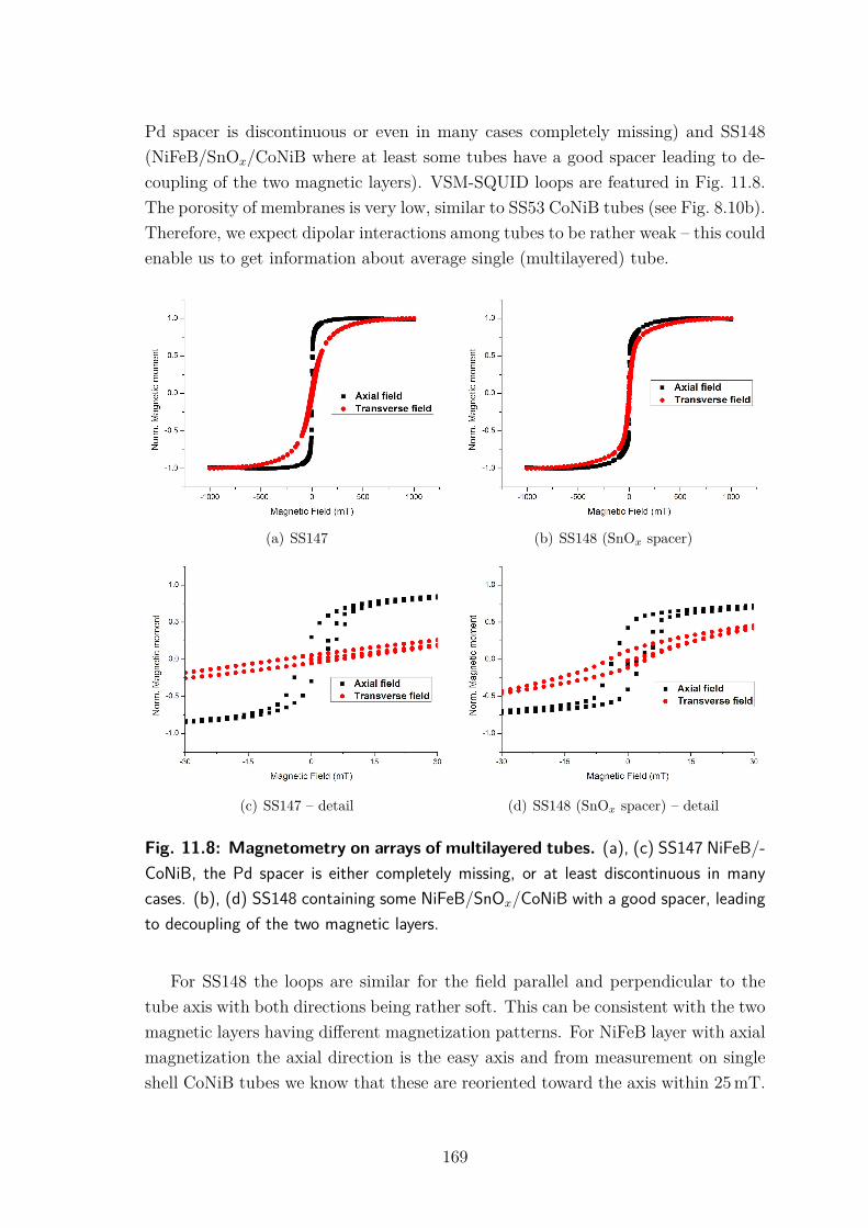
Pd spacer is discontinuous or even in many cases completely missing) and SS148(NiFeB/SnO𝑥/CoNiB where at least some tubes have a good spacer leading to de-coupling of the two magnetic layers). VSM-SQUID loops are featured in Fig. 11.8.The porosity of membranes is very low, similar to SS53 CoNiB tubes (see Fig. 8.10b).Therefore, we expect dipolar interactions among tubes to be rather weak – this couldenable us to get information about average single (multilayered) tube.
(a) SS147 (b) SS148 (SnO𝑥 spacer)
(c) SS147 – detail (d) SS148 (SnO𝑥 spacer) – detail
Fig. 11.8: Magnetometry on arrays of multilayered tubes. (a), (c) SS147 NiFeB/-CoNiB, the Pd spacer is either completely missing, or at least discontinuous in manycases. (b), (d) SS148 containing some NiFeB/SnO𝑥/CoNiB with a good spacer, leadingto decoupling of the two magnetic layers.
For SS148 the loops are similar for the field parallel and perpendicular to thetube axis with both directions being rather soft. This can be consistent with the twomagnetic layers having different magnetization patterns. For NiFeB layer with axialmagnetization the axial direction is the easy axis and from measurement on singleshell CoNiB tubes we know that these are reoriented toward the axis within 25 mT.
169

Easy reorientation in transverse field is also understandable due to the presence ofCoNiB with azimuthal anisotropy (transverse to tube axis).
For SS147 (magnetic layers in direct contact), XMCD-PEEM suggested that bothlayers are coupled and have azimuthal magnetization. Again easy axial reorientationcan within 25 mT seems reasonable. However, it is strange that the axial loops aremore squared than for SS148 and mainly that the transverse direction appear sohard.
The deviations from the expected behaviour could be partially caused by a non-proper removal of the film on top and bottom of the template with the tubes, and/orslightly bent membrane with the tubes. Also some of SS148 tubes have only theouter layer.
To conclude this part: we cannot clearly tell the quality of the spacer just fromthe global measurements in this case. Situation should be better for two mag-netic layers with both having axial magnetization (e.g. for smaller diameters below100 nm, or both layers from NiFeB) where two distinct switching events should oc-cur.
11.4 Annealing and towards synthetic ferrimag-nets
We also tried to image annealed SS148 multilayered tubes to get axial magnetiza-tion in both layers and possibly explore (anti)parallel alignment of magnetization inboth layers modelled in the previous chapter. Unfortunately, the spacer was eitherdamaged during the treatment, or the temperature was too low to recover axialmagnetization in the CoNiB layer. Here one can use spacer from different materialand of smaller thickness (possibly done by atomic layer deposition), or rather changethe composition of both magnetic layers to have the axial magnetization from thebeginning. One may think of e.g. NiFeB/SnO𝑥/NiFeB layer that should be feasibleto fabricate and with preferred axial magnetization direction for both layers. Onewould be still able to distinguish between parallel and antiparallel configuration, butthe layers could not be resolved independently. The easiest way might be keeping thesame chemical composition and just decreasing the diameter, as CoNiB nanotubeswith smaller diameter (e.g. 100 nm) were found to be axially magnetized (see sec-tion 8.4). Such downscaling is challenging, but feasible as both at TU Darmstadtand in our laboratory we could fabricate nanotubes with diameters around 100 nm(80 nm at TU Darmstadt).
Further, spacers with smaller thickness and from different materials could be ofinterest for investigation of magnetoresistance effects; SnO𝑥 that was employed in
170

our case is a conductive oxide (similar to indium tin oxide – ITO), thus one couldprefer either better metal, or insulating oxide (depending on the application). Weused SnO𝑥 for the ease of fabrication, but other spacers can be fabricated usingatomic layer deposition or solution-based methods.
11.5 Summary of investigation of multilayered tu-bes
We studied multilayered tubes with two magnetic layers with different chemicalcomposition separated a non-magnetic spacer (metallic or insulating), more pre-cisely NiFeB/(Pd)/CoNiB (SS147 sample) and NiFeB/SnO𝑥/CoNiB (SS148 sample)stacks.
In all cases the CoNiB layer resembled single-layered CoNiB tubes with similardiameter (e.g. SS53 sample): it contained multiple azimuthal domains. For SS147(NiFeB/CoNiB), the outer NiFeB layer displayed the same magnetization pattern,i.e. both layers were exchange-coupled due to the missing/damaged spacer. SS148,with SnO𝑥 spacer, displayed exchange-decoupled layers, where outer NiFeB wasaxially magnetized and the inner CoNiB exhibited azimuthal magnetization. Weobserved effect of both pulse and quasistatic magnetic field on the tubes. Short highfield value (100 mT, ms duration) pulses led to switching of magnetization in bothlayers with azimuthal domains surprisingly staying at the same place, just reversingthe circulation sense. Quasistatic field of increasing value resulted in the reversalof the outer NiFeB shell by a propagation of a strange magnetic configuration (notproperly understood). Some changes occurred also for the CoNiB layer – (dis)appearance and extension of some domains, but nothing clearly related to changesin the NiFeB shell.
Next steps could include the realization of a system with axial magnetizationin both layers (towards SAFs) and downscaling of the system, which is challenging,but feasible as both at TU Darmstadt and in our laboratory we could fabricatenanotubes with diameters as small as 100 nm (80 nm at TU Darmstadt).
171
12 CONCLUSION & PERSPECTIVE
We successfully fabricated nanotubes from several ferromagnetic materials by elec-trochemical methods in nanoporous templates. Namely we prepared NiCo nan-otubes (diameter 70-90 nm), Ni nanotubes (diameter around 60 nm) and nanostruc-tures with alternating wire (solid) and tube (hollow) segments. Further, we obtainedCoNiB and NiFeB electroless deposited tubes (diameters 80-400 nm) as well as mul-tilayered tubes from our collaborators in TU Darmstadt. Aside from these, wefabricated similar CoNiB nanotubes by the same technique (diameters 100-200 nm).
We investigated all these nanostructures with electron microscopy (scanning/-transmission) and in some cases also with atomic force microscopy. Aside from themorphology and topography investigation, we performed chemical analysis usingenergy-dispersive X-ray spectroscopy. In addition, we have some preliminary chem-ical analysis from our collaborators (CEMES, Toulouse and Spintec, Grenoble) byelectron energy loss spectroscopy. The key magnetic investigation was conductedwith a combination of various magnetic microscopies: electron holography, mag-netic force microscopy, and mainly X-ray magnetic circular dichroism microscopies(XMCD-PEEM and STXM). These were complemented with magnetometry on ar-rays and single structures. Our findings are supported by micromagnetic simulationsand numerical modelling of XMCD-PEEM images.
Electroless-deposited CoNiB and NiFeB tubes
In electroless-deposited CoNiB tubes (diameter around 300 nm), the XMCD-PEEMimaging and comparison with the numerical modelling revealed series of well-defineddomains with azimuthal magnetization separated by Bloch-type walls (radial mag-netization in the core). These flux-closure domains generate weak and very short-ranged stray fields, while being separated by narrow domain walls, significantlynarrower than the tube diameter. The domain wall density is as high as 5/µm.Assuming just the geometry, these long (up to 30 µm) tubes should be axially mag-netized. Thus, an additional contribution of magnetic anisotropy has to be present inorder to favour alignment of magnetization along the azimuthal direction (i.e. easyaxis for the azimuthal and hard axis for the longitudinal direction). The azimuthalanisotropy may originate from the growth-induced strain and/or grain shape. Wecannot also rule out the effect of rapid template dissolution.
When magnetic field is applied along the tube axis, the magnetization graduallyrotates towards the axial direction. Thanks to STXM imaging under such field wecould extract the strength of the anisotropy corresponding to an effective anisotropyconstant of approximately 10 kJ/m3. The anisotropy strength could be tailored
172
through annealing or material composition. I.e. after annealing at around 450∘C,the magnetization is axial and can be switched with several mT applied along thetube axis.
(Ni80Fe20)B tubes of similar geometry prepared in the same way are axially-magnetized even in the as-deposited state. Unlike CoNiB (significant negative mag-netostriction), NiFeB exhibits almost zero (tiny positive) magnetostriction. On thisbasis we put forward the magnetoelastic origin of azimuthal domains in the CoNiBtubes. We observed a switching of the magnetization in NiFeB tubes with magneticfield and the displacement of a domain boundary. In electron holography exper-iments complex phase maps were observed which we attribute to the large tubediameter (sometimes almost 400 nm) and field having significant transverse compo-nent with respect to the tube axis.
Another way how to obtain axial magnetization is to reduce the diameter. CoNiBnanotubes with diameter around 100 nm display longitudinal magnetization, bothin XMCD-PEEM and magnetic force microscopy imaging. Even though there mightbe some anisotropy present, the exchange energy for azimuthal magnetization wouldbe too high. Thus, axial magnetization is preferred.
Some nanotubes, mainly electroplated ones (NiCo, Ni) with thin shells (< 15 nm)could not be investigated properly by magnetic microscopies due to a very low signalresulting from the (partial) oxidation of the material. Such thin nanotubes shouldbe sandwiched in between protective layers, e.g. few nanometres of silica/hafnia de-posited by atomic layer deposition, or titania prepared by chemical bath deposition.
Aside from focusing on nanotubes we also probed more complex geometries:nanoelements with wire and tube segments and multilayered tubes (core-shell struc-tures).
Twires
Nanoelements with alternating nanowire and nanotube parts (outer diameter around60 nm) had very sharp wire/tube transitions (mostly gradual transition is reportedin the literature) with multiple tube segments with lengths even above 2 µm (longerthan found in the literature). Unfortunately, the structure proved to be quite chal-lenging for the first magnetic microscopy imaging. Small diameter with low Nimagnetic moment gave weak magnetic signal for nanowire parts, not speaking ofthe tubular segments. In more sensitive XMCD-PEEM we had problems with lo-calizing suitable structures as well as with the limited spatial resolution and imageanalysis due to a high curvature. Yet, with slightly larger structures (thicker) con-taining Fe or Co (higher magnetic moment), one may test experimentally numerical
173

and theoretical predictions regarding these intriguing structures combining wire andtube segments.
Multilayered tubes (core-shell structures)
For potential (spintronic) devices (e.g. sensors), one would need to use multilayeredtubes (core-shell structures), not just simple tubes. Along this line, in collaborationwith TU Darmstadt we prepared multilayered tubes with two different magneticlayers separated by a non-magnetic spacer (NiFeB/SnO𝑥/CoNiB). Thanks to theelement specificity of XMCD-PEEM we could probe separately each magnetic layer.These were found to be exchange-decoupled. Anisotropy of each individual shellprevailed. Therefore, CoNiB had azimuthal domains, whereas NiFeB axial magne-tization. Further, we probed switching of the tubes by magnetic field. With staticmagnetic field we saw reversal of NiFeB through the nucleation and propagation ofa domain boundary. There were also some changes in CoNiB, but these could notbe clearly correlated with NiFeB state except for the effect of stray field emanatingfrom a domain wall in the NiFeB layer. More interesting were experiments with fieldpulses when the field was applied with some angle versus the common tube axis. Toour surprise, not only NiFeB switched, but also circulation of all domains in CoNiBwas reversed.
Aside from experiments we also run micromagnetic simulations of multilayeredtubes with a thicker spacer (e.g. 10 nm). Here we could demonstrate antiparallelordering of axially-magnetized domains in both magnetic layers through dipolarinteraction as well as obtain some intriguing coupled vortex-like walls in both tubes.
Despite providing only preliminary results in some cases, we believe that wehave shown versatility of magnetic nanotubes. Through changing the composition,geometry or annealing one can obtain domains almost á la carte: azimuthal or axialones with both being useful. Especially azimuthal domains are interesting owing tothe magnetic flux-closure that could be exploited in magnetic sensors or in devicesbased on dense arrays of elements. Both hollow nature and azimuthal domains wouldsignificantly decreases interaction between these elements and unwanted cross-talk.Properties and viability of tubes can be further enhanced by preparing core-shellstructures / tubular multilayers.
174
Perspective
Nanotubes with azimuthal domains
CoNiB tubes with azimuthal domains and many domain walls may open the wayfor the experimental study of domain wall motion in nanotubes as well as novelphenomena predicted in curved geometries. Our CoNiB tubes with azimuthal do-mains could be a good system for experimental test of recent theoretical predictionsof the non-reciprocity of spin-wave propagation in magnetic nanotubes [35, 36]. Inboth cases (DWs & spin waves), the intermediate challenge would be to controlthe size and number of azimuthal domains as the simpler system would be easierfor fundamental investigations. Later one could think of designing new magnon-ics wave-guides utilizing core-shell structures with inner core having segments fromdifferent (ferromagnetic) materials forming a magnonic crystal. One can also con-sider the CoNiB tubes with flux-closure domains and very narrow domain walls asa building block of the racetrack memory as array of such structures would havesmaller cross-talk and it would be easier to fabricate than vertical strips. As for theminiaturization of the tubes, one could prepare azimuthal domains in even smallernanotubes by tuning the geometry and material. However, we do not expect thatone can go significantly below 100 nm-diameter for high aspect ratio nanotubes,while keeping the azimuthal magnetization.
Multilayered tubes
We have demonstrated possibility of fabrication of multilayered tubes with a thicknon-magnetic spacer. The further development could focus on effects already knownfrom flat multilayers, but not implemented so far in the curved tubular geometry.I.e. on the Spin Hall effect and the Dzyaloshinskii-Moriya interaction in magneticnanotubes with e.g. Pt core (bilayer). As already outlined in the introduction,one can also combine effective DMI interaction arising from the curvature withthe one coming from interfaces with heavy metals/oxides. Further, one can real-ize tubular version of synthetic antiferromagnets and trilayers for giant or tunnelmagnetoresistance elements that are important for various sensors. These wouldrequire continuous spacer (such as our SnO𝑥), however, with smaller thickness (fewnm instead of 10-20 nm). Such thin spacer layer could be prepared by atomic layerdeposition, which can provide both insulators and metals. Longer term challengecould be again the miniaturization (decrease of diameter) of the tubular structures.For sure one could prepare several of the above-mentioned structure by depositionof layers on (vertical) pillars, but here we have in mind rather preparation of largevertical arrays of such structures in ordered porous templates.
175

Tubular magnetic racetrack memory
Now we briefly return to the idea of the domain wall memory proposed by IBM [2].The proposal gradually evolved from simple permalloy tracks towards more complexheterostructures (multilayers) and shifting of DWs by electric current instead ofmagnetic field.
Until the racetrack memory 4.0 based on synthetic antiferromagnetic (SAF)strips [5], the issues of dipolar interaction among the magnetic tracks was not prop-erly addressed. This is partially caused by the fact that most experiments were per-formed utilizing 2D tracks on flat substrates, where dipolar fields are short-rangedespecially for ultrathin films with perpendicular magnetization. This is no longerthe case for the 3D concept, where longer-ranged dipolar fields arise. Even thoughthe concept of SAF has been demonstrated on a flat substrate, the idea about mak-ing such tracks vertical to have a proper 3D device is rather vague. It was admittedthat fabrication of vertical tracks is “outstanding challenge” [5]. The possible solu-tion put forward by Parkin is atomic layer deposition of vertical strips. However,fabrication of such 3D multilayered strips utilizing ALD or other techniques doesnot seem to be viable. In addition there are still some question-marks regarding thematerial properties (especially magnetic ones) of the ALD layers that tend to bevery granular.
Here we propose racetrack memory based on magnetic nanotubes. First, evensimple tubes with axially-magnetized domains (i.e. analogy of Parkin’s racetrack1.0) could be of interest for racetrack or other devices as it has been shown thatinteraction among tubes in arrays is significantly smaller than for solid wires (withthe same diameter and spacing) [215]. In our work we experimentally show that theCoNiB tubes can sustain many azimuthal domains even for long tubes. These flux-closure domains significantly reduce the dipolar interactions among closely spacedtracks as DWs bear no net magnetic charge. In addition, the DWs separating suchdomains in our tubes are very narrow, significantly smaller than the tube diameteritself (see Fig. 8.6). Further, as regards the fabrication, vertical arrays of tubeshave been already synthesized in (ordered) porous templates by chemical methodsby many groups, while array of vertical strips remains on a paper.
Therefore, for the tubular racetracks one can either utilize tubes with single mag-netic layer having azimuthal magnetization, or one can even return to the Parkin’sidea of SAF layers, however, in the form of multilayered tubes, not flat strips. Un-like vertical strips, one can fabricate SAF in tubular geometry by combining elec-trochemistry (e.g. electroless plating as shown in our work) for the magnetic layersand atomic layer deposition for the non-magnetic Ru spacer, or maybe the wholestructure can be realized by ALD using direct deposition of metals [133]. In case of
176
tubular SAF, we are no longer considering azimuthal domains, but rather axial orradial ones (magnetization perpendicular to the tube surface). Therefore, one couldpossibly realize vertical SAF this way and even in the tubular geometry, openingways to study new and enhanced phenomena predicted for curved geometries.
In our work we investigated similar multilayered system: we obtained two mag-netic layers separated by a non-magnetic spacer (chapter 11). Therefore, the syn-thesis of vertical array of multilayered tubes is feasible. In the future, the tubularSAF could be realized by making thinner spacers and possibly employing differentmaterials.
We have been concerned with magnetic nanotubes, cylindrical structures witha hollow core. The curvature and the core give them interesting properties thatcould be possibly exploited in 3D spintronics, be it solid state memory, advancedsensors or magnonics crystals for spin waveguides, all based on (arrays of vertical)multilayered tubes or core-shell nanowires.
177
BIBLIOGRAPHY
[1] Parkin, S. Shiftable magnetic shift register and method of using the same(2004). URL http://www.google.com/patents/US6834005. US Patent6,834,005.
[2] Parkin, S. S., Hayashi, M. & Thomas, L. Magnetic domain-wall racetrackmemory. Science 320, 190–194 (2008).
[3] Suto, H. et al. Three-dimensional magnetic recording using ferromagneticresonance. Jpn. J. Appl. Phys. 55, 07MA01 (2016). URL http://stacks.iop.org/1347-4065/55/i=7S3/a=07MA01.
[4] Okamoto, S., Kikuchi, N., Furuta, M., Kitakami, O. & Shimatsu, T. Mi-crowave assisted magnetic recording technologies and related physics. J.Phys. D: Appl. Phys. 48, 353001 (2015). URL http://stacks.iop.org/0022-3727/48/i=35/a=353001.
[5] Parkin, S. & Yang, S.-H. Memory on the racetrack. Nat. Nanotechnol. 10,195–198 (2015).
[6] Vázquez, M. (ed.) Magnetic nano-and microwires: design, synthesis, proper-ties and applications, vol. 80 of Woodhead Publishing Series in Electronic andOptical Materials (Woodhead Publishing, 2015).
[7] Streubel, R. et al. Magnetism in curved geometries. J. Phys. D: Appl. Phys.49, 363001 (2016). URL http://stacks.iop.org/0022-3727/49/i=36/a=363001.
[8] Fernández-Pacheco, A. et al. Three-dimensional nanomagnetism. Nat. Com-mun. 8, 15756 (2017).
[9] Baraduc, C., Chshiev, M. & Dieny, B. Spintronic phenomena: Giant mag-netoresistance, tunnel magnetoresistance and spin transfer torque. In Gi-ant Magnetoresistance (GMR) Sensors, 1–30 (Springer, 2013). URL https://doi.org/10.1007/978-3-642-37172-1_1.
[10] Thomas, L. & Parkin, S. Current induced domain-wall motion in magneticnanowires, vol. 2 - Micromagnetism of Handbook of Magnetism and AdvancedMagnetic Materials, chap. Magnetic configurations in small elements, magne-tization processes and hysteretic properties (John Wiley & Sons, Ltd, 2007).URL http://dx.doi.org/10.1002/9780470022184.hmm210.
178
[11] Wegrowe, J.-E., Kelly, D., Franck, A., Gilbert, S. E. & Ansermet, J.-P. Mag-netoresistance of ferromagnetic nanowires. Phys. Rev. Lett. 82, 3681–3684(1999). URL http://link.aps.org/doi/10.1103/PhysRevLett.82.3681.
[12] Wernsdorfer, W. et al. Nucleation of magnetization reversal in individualnanosized nickel wires. Phys. Rev. Lett. 77, 1873 (1996).
[13] Bran, C. et al. Spin configuration of cylindrical bamboo-like magneticnanowires. J. Mater. Chem. C 4, 978–984 (2016). URL http://dx.doi.org/10.1039/C5TC04194E.
[14] Biziere, N. et al. Imaging the fine structure of a magnetic domain wall in a Ninanocylinder. Nano Lett. 13, 2053–2057 (2013).
[15] Da Col, S. et al. Observation of Bloch-point domain walls in cylindrical mag-netic nanowires. Phys. Rev. B 89, 180405 (2014).
[16] Thiaville, A. & Nakatani, Y. Domain-Wall Dynamics in Nanowires andNanostrips, 161–205 (Springer Berlin Heidelberg, Berlin, Heidelberg, 2006).URL http://dx.doi.org/10.1007/10938171_5.
[17] Yan, M., Kákay, A., Gliga, S. & Hertel, R. Beating the Walker limit withmassless domain walls in cylindrical nanowires. Phys. Rev. Lett. 104, 057201(2010).
[18] Son, S. J., Reichel, J., He, B., Schuchman, M. & Lee, S. B. Magnetic nanotubesfor magnetic-field-assisted bioseparation, biointeraction, and drug delivery. J.Am. Chem. Soc. 127, 7316–7317 (2005).
[19] Li, X.-Z., Wu, K.-L., Ye, Y. & Wei, X.-W. Controllable synthesis of Ni nano-tube arrays and their structure-dependent catalytic activity toward dye degra-dation. CrystEngComm 16, 4406–4413 (2014).
[20] Usov, N., Zhukov, A. & Gonzalez, J. Domain walls and magnetization reversalprocess in soft magnetic nanowires and nanotubes. J. Magn. Magn. Mater.316, 255–261 (2007).
[21] Sun, C. & Pokrovsky, V. L. Magnetic properties of a long, thin-walled ferro-magnetic nanotube. J. Magn. Magn. Mater. 355, 121 – 130 (2014). URL http://www.sciencedirect.com/science/article/pii/S0304885313009049.
[22] Yan, M., Andreas, C., Kákay, A., García-Sánchez, F. & Hertel, R. Fast domainwall dynamics in magnetic nanotubes: Suppression of Walker breakdown andCherenkov-like spin wave emission. Appl. Phys. Lett. 99, 122505 (2011).
179
[23] Kimling, J. et al. Photoemission electron microscopy of three-dimensionalmagnetization configurations in core-shell nanostructures. Phys. Rev. B84, 174406 (2011). URL http://link.aps.org/doi/10.1103/PhysRevB.84.174406.
[24] Pitzschel, K. et al. Magnetic reversal of cylindrical nickel nanowires withmodulated diameters. J. Appl. Phys. 109, 033907 (2011). URL https://doi.org/10.1063/1.3544036.
[25] Sekhar, M. C. et al. Helical domain walls in constricted cylindrical nifenanowires. Appl. Phys. Lett. 101, 152406 (2012). URL https://doi.org/10.1063/1.4758469.
[26] Ivanov, Y. P., Chuvilin, A., Lopatin, S. & Kosel, J. Modulated magneticnanowires for controlling domain wall motion: Toward 3D magnetic memories.ACS Nano 10, 5326–5332 (2016).
[27] Davis, D. M. et al. Magnetoresistance in electrodeposited CoNiFe/Cu multi-layered nanotubes. Electrochem. Solid-State Lett. 9, C153–C155 (2006). URLhttp://esl.ecsdl.org/content/9/9/C153.abstract. http://esl.ecsdl.org/content/9/9/C153.full.pdf+html.
[28] Pitzschel, K. et al. Controlled introduction of diameter modulations in arrayedmagnetic iron oxide nanotubes. ACS Nano 3, 3463–3468 (2009).
[29] Philippe, L. & Michler, J. A kinetic model enabling controlled electrosynthesisof stacked metallic nanotubes and nanowires. Small 4, 904–907 (2008).
[30] Neumann, R. F. et al. Tailoring the nucleation of domain walls along multi-segmented cylindrical nanoelements. Nanotechnology 26, 215701 (2015). URLhttp://stacks.iop.org/0957-4484/26/i=21/a=215701.
[31] Rohan, J. F. et al. Coaxial metal and magnetic alloy nanotubes in polycar-bonate templates by electroless deposition. Electrochem. Commun. 10, 1419 –1422 (2008). URL http://www.sciencedirect.com/science/article/pii/S1388248108003020.
[32] Emori, S., Bauer, U., Ahn, S.-M., Martinez, E. & Beach, G. S. Current-driven dynamics of chiral ferromagnetic domain walls. Nat. Mater. 12, 611–616 (2013).
[33] Belmeguenai, M. et al. Interfacial Dzyaloshinskii-Moriya interaction in per-pendicularly magnetized Pt/Co/AlO𝑥 ultrathin films measured by brillouin
180
light spectroscopy. Phys. Rev. B 91, 180405 (2015). URL https://link.aps.org/doi/10.1103/PhysRevB.91.180405.
[34] Hertel, R. Curvature-induced magnetochirality. SPIN 03, 1340009 (2013).URL http://dx.doi.org/10.1142/S2010324713400092.
[35] Otálora, J. A., Yan, M., Schultheiss, H., Hertel, R. & Kákay, A.Curvature-induced asymmetric spin-wave dispersion. Phys. Rev. Lett. 117,227203 (2016). URL http://link.aps.org/doi/10.1103/PhysRevLett.117.227203.
[36] Otálora, J. A., Yan, M., Schultheiss, H., Hertel, R. & Kákay, A. Asymmetricspin-wave dispersion in ferromagnetic nanotubes induced by surface curvature.Phys. Rev. B 95, 184415 (2017). URL https://link.aps.org/doi/10.1103/PhysRevB.95.184415.
[37] Chan, K. T., Doran, C., Shipton, E. G. & Fullerton, E. E. Core-shell structurednanowire spin valves. IEEE Trans. Magn. 46, 2209–2211 (2010).
[38] Dyakonov, M. I. Spin hall effect. arXiv:1210.3200 (2012).
[39] Hirsch, J. E. Spin hall effect. Phys. Rev. Lett. 83, 1834–1837 (1999).
[40] Hu, C. D. The Dzyaloshinskii-Moriya interaction in metals. J. Phys. Condens.Matter 24, 086001 (2012). URL http://stacks.iop.org/0953-8984/24/i=8/a=086001.
[41] Kronmüller, H. & Parkin, S. (eds.) Fundamentals and Theory, vol. 1 of Hand-book of Magnetism and Advanced Magnetic Materials (Wiley, 2007).
[42] Blundell, S. Magnetism in condensed matter. Oxford master series in con-densed matter physics (Oxford, 2001).
[43] Coey, J. M. D. Magnetism and magnetic materials (Cambridge UniversityPress, 2010).
[44] MacDonald, A. & Tsoi, M. Antiferromagnetic metal spintronics. Phil. Trans.R. Soc. A 369, 3098–3114 (2011).
[45] Jungwirth, T., Marti, X., Wadley, P. & Wunderlich, J. Antiferromagneticspintronics. Nat. Nanotechnol. 11, 231–241 (2016).
[46] Stanciu, C. D. et al. Ultrafast spin dynamics across compensation points in fer-rimagnetic GdFeCo: The role of angular momentum compensation. Phys. Rev.
181
B 73, 220402 (2006). URL https://link.aps.org/doi/10.1103/PhysRevB.73.220402.
[47] Kim, K.-J. et al. Fast domain wall motion induced by antiferromagnetic spindynamics at the angular momentum compensation temperature of ferrimag-nets. arXiv:1703.07515 (2017).
[48] Oh, S.-H. et al. Coherent terahertz spin-wave emission associated with ferri-magnetic domain wall dynamics. arXiv:1706.00549 (2017).
[49] Faure-Vincent, J. et al. Interlayer magnetic coupling interactions of two fer-romagnetic layers by spin polarized tunneling. Phys. Rev. Lett. 89, 107206(2002).
[50] Bruno, P. Theory of interlayer exchange interactions in magnetic multilayers.J. Phys. Condens. Matter 11, 9403 (1999). URL http://stacks.iop.org/0953-8984/11/i=48/a=305.
[51] Yang, S.-H., Ryu, K.-S. & Parkin, S. Domain-wall velocities of up to 750 m s−1
driven by exchange-coupling torque in synthetic antiferromagnets. Nat. Nan-otechnol. 10, 221–226 (2015).
[52] Yang, S.-H. & Parkin, S. Novel domain wall dynamics in synthetic anti-ferromagnets. J. Phys. Condens. Matter 29, 303001 (2017). URL http://stacks.iop.org/0953-8984/29/i=30/a=303001.
[53] Lepadatu, S. et al. Synthetic ferrimagnet nanowires with very low criticalcurrent density for coupled domain wall motion. Sci. Rep. 7, 1640 (2017).
[54] Hubert, A. & Schäfer, R. Magnetic domains: The Analysis of Magnetic Mi-crostructures (Springer, 2009), 3rd edn.
[55] Guimarães, A. P. Principles of Nanomagnetism. NanoScience and Technology(Springer, 2009).
[56] Fruchart, O. Lecture notes on nanomagnetism. PDF (2016). Available fromhttp://fruchart.eu/olivier/lectures/nanomagnetism-2016-11-04.pdf, [Accessed 2017-04-30].
[57] Sandratskii, L. M. Insight into the Dzyaloshinskii-Moriya interaction throughfirst-principles study of chiral magnetic structures. Phys. Rev. B 96, 024450(2017). URL https://link.aps.org/doi/10.1103/PhysRevB.96.024450.
182
[58] Bogdanov, A. & Hubert, A. Thermodynamically stable magnetic vor-tex states in magnetic crystals. J. Magn. Magn. Mater. 138, 255 –269 (1994). URL http://www.sciencedirect.com/science/article/pii/0304885394900469.
[59] Rohart, S. & Thiaville, A. Skyrmion confinement in ultrathin film nanos-tructures in the presence of Dzyaloshinskii-Moriya interaction. Phys. Rev. B88, 184422 (2013). URL https://link.aps.org/doi/10.1103/PhysRevB.88.184422.
[60] Goussev, A., Robbins, J., Slastikov, V. & Tretiakov, O. A. Dzyaloshinskii-Moriya domain walls in magnetic nanotubes. Phys. Rev. B 93, 054418 (2016).
[61] Stöhr, J. & Siegmann, H. C. (eds.) Magnetism: From Fundamentals toNanoscale Dynamics, vol. 152 of Solid-State Sciences (Springer, 2006).
[62] Ralph, D. C. & Stiles, M. D. Spin transfer torques. J. Magn. Magn. Mater.320, 1190–1216 (2008).
[63] Garello, K. et al. Symmetry and magnitude of spin-orbit torques in ferromag-netic heterostructures. Nat. Nanotechnol. 8, 587–593 (2013).
[64] Safeer, C. et al. Spin–orbit torque magnetization switching controlled by ge-ometry. Nat. Nanotechnol. 11, 143–146 (2016).
[65] Abert, C., Bruckner, F., Vogler, C. & Suess, D. Efficient micromagnetic mod-elling of spin-transfer torque and spin-orbit torque. AIP Adv. 8, 056008 (2018).URL https://doi.org/10.1063/1.5006561.
[66] Xu, F. et al. Enhanced film thickness for Néel wall in soft magnetic film byintroducing strong magnetocrystalline anisotropy. Sci. Rep. 6 (2016).
[67] Forster, H. et al. Micromagnetic simulation of domain wall motion in magneticnano-wires. J. Magn. Magn. Mater. 249, 181–186 (2002). URL http://www.sciencedirect.com/science/article/pii/S0304885302005280. Interna-tional Workshop on Magnetic Wires.
[68] Hertel, R. Computational micromagnetism of magnetization processes innickel nanowires. J. Magn. Magn. Mater. 249, 251–256 (2002).
[69] Han, D.-S. et al. Magnetic domain-wall motion by propagating spin waves.Appl. Phys. Lett. 94, 112502 (2009). URL http://dx.doi.org/10.1063/1.3098409.
183
[70] Wang, W. et al. Magnon-driven domain-wall motion with the Dzyaloshinskii-Moriya interaction. Phys. Rev. Lett. 114, 087203 (2015). URL https://link.aps.org/doi/10.1103/PhysRevLett.114.087203.
[71] Moretti, S., Raposo, V., Martinez, E. & Lopez-Diaz, L. Domain wall motionby localized temperature gradients. Phys. Rev. B 95, 064419 (2017). URLhttps://link.aps.org/doi/10.1103/PhysRevB.95.064419.
[72] Bryan, M. T., Dean, J. & Allwood, D. A. Dynamics of stress-induced domainwall motion. Phys. Rev. B 85, 144411 (2012). URL https://link.aps.org/doi/10.1103/PhysRevB.85.144411.
[73] Dean, J. et al. A sound idea: Manipulating domain walls in magneticnanowires using surface acoustic waves. Appl. Phys. Lett. 107, 142405 (2015).URL http://dx.doi.org/10.1063/1.4932057.
[74] Schryer, N. L. & Walker, L. R. The motion of 180∘ domain walls in uniformdc magnetic fields. J. Appl. Phys. 45, 5406–5421 (1974).
[75] Hagelberg, F. Magnetism in Carbon Nanostructures (Cambridge UniversityPress, 2017).
[76] Escrig, J., Landeros, P., Altbir, D., Vogel, E. & Vargas, P. Phase diagrams ofmagnetic nanotubes. J. Magn. Magn. Mater. 308, 233–237 (2007).
[77] Landeros, P., Suarez, O. J., Cuchillo, A. & Vargas, P. Equilibrium statesand vortex domain wall nucleation in ferromagnetic nanotubes. Phys. Rev.B 79, 024404 (2009). URL http://link.aps.org/doi/10.1103/PhysRevB.79.024404.
[78] Chen, A., Usov, N., Blanco, J. & Gonzalez, J. Equilibrium magnetiza-tion states in magnetic nanotubes and their evolution in external magneticfield. J. Magn. Magn. Mater. 316, e317 – e319 (2007). URL http://www.sciencedirect.com/science/article/pii/S0304885307002466. Proceed-ings of the Joint European Magnetic Symposia.
[79] Wyss, M. et al. Imaging magnetic vortex configurations in ferromagnetic nan-otubes. Phys. Rev. B 96, 024423 (2017). URL https://link.aps.org/doi/10.1103/PhysRevB.96.024423.
[80] Li, D., Thompson, R. S., Bergmann, G. & Lu, J. G. Template-based synthesisand magnetic properties of cobalt nanotube arrays. Adv. Mater. 20, 4575–4578(2008).
184
[81] Landeros, P. et al. Reversal modes in magnetic nanotubes. Appl. Phys.Lett. 90, 102501 (2007). URL http://scitation.aip.org/content/aip/journal/apl/90/10/10.1063/1.2437655.
[82] Bachmann, J. et al. Size effects in ordered arrays of magnetic nanotubes:Pick your reversal mode. J. Appl. Phys. 105, 07B521 (2009). URL http://dx.doi.org/10.1063/1.3074109.
[83] Allende, S., Escrig, J., Altbir, D., Salcedo, E. & Bahiana, M. Angular depen-dence of the transverse and vortex modes in magnetic nanotubes. Eur. Phys.J. B 66, 37–40 (2008).
[84] Albrecht, O. et al. Experimental evidence for an angular dependent transitionof magnetization reversal modes in magnetic nanotubes. J. Appl. Phys. 109,093910 (2011).
[85] Allende, S. & Arias, R. Transverse domain wall propagation in modulatedcylindrical nanostructures and possible geometric control. Phys. Rev. B 83,174452 (2011).
[86] Otálora, J., Lopez-Lopez, J., Vargas, P. & Landeros, P. Chirality switchingand propagation control of a vortex domain wall in ferromagnetic nanotubes.Appl. Phys. Lett. 100, 072407 (2012).
[87] Yan, M., Andreas, C., Kákay, A., García-Sánchez, F. & Hertel, R. Chiralsymmetry breaking and pair-creation mediated walker breakdown in magneticnanotubes. Appl. Phys. Lett. 100, 252401 (2012).
[88] Yang, J. et al. Characteristic dynamic modes and domain-wall motion inmagnetic nanotubes excited by resonant rotating magnetic fields. Phys. Rev.B 94, 024425 (2016).
[89] Otálora, J., López-López, J., Núñez, A. & Landeros, P. Domain wall manip-ulation in magnetic nanotubes induced by electric current pulses. J. Phys.:Condens. Matter 24, 436007 (2012).
[90] Yang, J., Yoo, M.-W. & Kim, S.-K. Spin-wave-driven high-speed domain-wallmotions in soft magnetic nanotubes. J. Appl. Phys. 118, 163902 (2015).
[91] López-López, J., Cortés-Ortuño, D. & Landeros, P. Role of anisotropy on thedomain wall properties of ferromagnetic nanotubes. J. Magn. Magn. Mater.324, 2024–2029 (2012).
185
[92] Lee, D., Cohen, R. E. & Rubner, M. F. Heterostructured magnetic nanotubes.Langmuir 23, 123–129 (2007).
[93] Betancourt, I., Hrkac, G. & Schrefl, T. Micromagnetic simulation of domainwall dynamics in permalloy nanotubes at high frequencies. J. Appl. Phys. 104,023915 (2008).
[94] Streubel, R. et al. Magnetic microstructure of rolled-up single-layer ferro-magnetic nanomembranes. Adv. Mater. 26, 316–323 (2014). URL http://dx.doi.org/10.1002/adma.201303003.
[95] Chen, A., Gonzalez, J. & Guslienko, K. Domain walls confined in magneticnanotubes with uniaxial anisotropy. J. Magn. Magn. Mater. 324, 3912 –3917 (2012). URL http://www.sciencedirect.com/science/article/pii/S0304885312005410.
[96] Daub, M., Knez, M., Goesele, U. & Nielsch, K. Ferromagnetic nanotubes byatomic layer deposition in anodic alumina membranes. J. Appl. Phys. 101,09J111 (2007).
[97] Proenca, M. et al. Magnetic interactions and reversal mechanisms in Co na-nowire and nanotube arrays. J. Appl. Phys. 113, 093907 (2013).
[98] Vansteenkiste, A. et al. The design and verification of MuMax3. AIP Adv. 4,107133 (2014).
[99] Richardson, D. & Rhen, F. M. F. Increasing the magnetization of electrolesslydeposited Ni–B nanotubes. IEEE Trans. Magn. 51, 1–4 (2015).
[100] Pathak, S., Hong, J., Chaudhary, J. & Sharma, M. Magneto-optical Kerr ef-fect characterization of electrodeposited Y-junction magnetic nanostructures.J. Appl. Phys. 117, 17A751 (2015). URL http://dx.doi.org/10.1063/1.4918952.
[101] Tabasum, M. R. et al. Magnetic force microscopy investigation of arrays ofnickel nanowires and nanotubes. Nanotechnology 25, 245707 (2014). URLhttp://stacks.iop.org/0957-4484/25/i=24/a=245707.
[102] Wang, T., Wang, Y., Li, F., Xu, C. & Zhou, D. Morphology and magneticbehaviour of an Fe3O4 nanotube array. J. Phys.: Condens. Matter 18, 10545–10551 (2006).
186
[103] Li, F. S. et al. Fabrication and magnetic properties of FeCo alloy nanotubearray. J. Appl. Phys. 101, 014309 (2007). URL http://dx.doi.org/10.1063/1.2405729.
[104] Kozlovskiy, A. et al. Study of Ni/Fe nanotube properties. Nucl. Instrum.Methods Phys. Res., Sect. B 365, 663 – 667 (2015). URL http://www.sciencedirect.com/science/article/pii/S0168583X15009635. SwiftHeavy Ions in Matter, 18-21 May, 2015, Darmstadt, Germany.
[105] Wang, Z. K. et al. Spin waves in nickel nanorings of large aspect ratio. Phys.Rev. Lett. 94, 137208 (2005). URL https://link.aps.org/doi/10.1103/PhysRevLett.94.137208.
[106] Nguyen, T. & Cottam, M. Spin-wave excitations in ferromagnetic nanotubes.Surf. Sci. 600, 4151 – 4154 (2006). URL http://www.sciencedirect.com/science/article/pii/S0039602806004870.
[107] González, A., Landeros, P. & Núñez, Á. S. Spin wave spectrum of magneticnanotubes. J. Magn. Magn. Mater. 322, 530 – 535 (2010). URL http://www.sciencedirect.com/science/article/pii/S0304885309010117.
[108] Buchter, A. et al. Reversal mechanism of an individual Ni nanotube simulta-neously studied by torque and SQUID magnetometry. Phys. Rev. Lett. 111,067202 (2013). URL https://link.aps.org/doi/10.1103/PhysRevLett.111.067202.
[109] Diehle, P., Caron, J., Kovács, A., Ungermann, J. & Dunin-Borkowski, R. E.Towards electron holographic tomography of three-dimensional magnetiza-tion distributions in ferromagnetic nanotubes (2015). URL http://www.rafaldb.com/posters/pics2015/04g.pdf. Presented at the 3rd Interna-tional Conference on Frontiers of Aberration Corrected Electron Microscopy"PICO 2015", Kasteel Valsbroek, The Netherlands. Available from http://www.rafaldb.com/posters/pics2015/04g.pdf [accessed 2017-04-04].
[110] Ruffer, D. et al. Magnetic states of an individual Ni nanotube probed byanisotropic magnetoresistance. Nanoscale 4, 4989–4995 (2012). URL http://dx.doi.org/10.1039/C2NR31086D.
[111] Baumgaertl, K. et al. Magnetization reversal in individual Py and CoFeBnanotubes locally probed via anisotropic magnetoresistance and anomalousNernst effect. Appl. Phys. Lett. 108 (2016). URL http://scitation.aip.org/content/aip/journal/apl/108/13/10.1063/1.4945331.
187

[112] Jia, C.-J. et al. Single-crystalline iron oxide nanotubes. Angew. Chem. Int. Ed.44, 4328–4333 (2005). URL http://dx.doi.org/10.1002/anie.200463038.
[113] Mertig, M., Kirsch, R. & Pompe, W. Biomolecular approach to nanotubefabrication. Appl. Phys. A 66, S723–S727 (1998).
[114] Khan, A. A. Tobacco Mosaic Virus (TMV) as a Nanoscaffold for InorganicAssemblies. Ph.D. thesis, University of Basque Country (2012).
[115] Apel, P. Y. & Dmitriev, S. Micro-and nanoporous materials produced usingaccelerated heavy ion beams. Adv. Nat. Sci.: Nanosci. Nanotechnol. 2, 013002(2011).
[116] Masuda, H. Highly Ordered Nanohole Arrays in Anodic Porous Alumina,37–55 (Springer, Boston, MA, 2005). URL http://dx.doi.org/10.1007/0-387-25193-6_3.
[117] Vogel, E. E., Vargas, P., Altbir, D. & Escrig, J. 14 - magnetic nanotubes.In Sattler, K. D. (ed.) Handbook of nanophysics: nanotubes and nanowires,14–1–14–13 (CRC press, 2010).
[118] Ye, Y. & Geng, B. Magnetic nanotubes: Synthesis, properties, and ap-plications. Crit. Rev. Solid State Mater. Sci. 37, 75–93 (2012). URLhttp://dx.doi.org/10.1080/10408436.2011.613491.
[119] Proenca, M., Sousa, C., Ventura, J. & Araújo, J. 24 - Electrochemical syn-thesis and magnetism of magnetic nanotubes. In Vázquez, M. (ed.) MagneticNano- and Microwires, Woodhead Publishing Series in Electronic and Opti-cal Materials, 727 – 781 (Woodhead Publishing, 2015). URL http://www.sciencedirect.com/science/article/pii/B9780081001646000242.
[120] Huang, Y.-C. et al. Fabrication and magnetic properties of 100-nm-scaledpermalloy nanotube arrays. J. Vac. Sci. Technol., B 30, 06FF07 (2012). URLhttp://dx.doi.org/10.1116/1.4762843.
[121] Wang, X. W., Yuan, Z. H. & Fang, B. C. Template-based synthesis andmagnetic properties of Ni nanotube arrays with different diameters. Mater.Chem. Phys. 125, 1–4 (2011).
[122] Atalay, F. et al. The effect of back electrode on the formation of electrode-posited CoNiFe magnetic nanotubes and nanowires. Appl. Surf. Sci. 256, 2414– 2418 (2010). URL http://www.sciencedirect.com/science/article/pii/S0169433209015220.
188

[123] Proenca, M., Sousa, C., Ventura, J., Vazquez, M. & Araujo, J. Distinguish-ing nanowire and nanotube formation by the deposition current transients.Nanoscale Res. Lett. 7, 280 (2012). URL http://www.nanoscalereslett.com/content/7/1/280.
[124] Bao, J. et al. Template synthesis of an array of nickel nanotubules and itsmagnetic behavior. Adv. Mater. 13, 1631–1633 (2001).
[125] Fukunaka, Y., Motoyama, M., Konishi, Y. & Ishii, R. Producing shape-controlled metal nanowires and nanotubes by an electrochemical method. Elec-trochem. Solid State Lett. 9, C62–C64 (2006).
[126] Li, Y. L. et al. Fabrication and magnetic properties of free-standing Ni na-notube arrays with controllable wall thickness. Appl. Phys. Lett. 100, 052402(2012). URL http://dx.doi.org/10.1063/1.3681136.
[127] Schaefer, S. et al. NiCo nanotubes plated on Pd seeds as a designed magnet-ically recollectable catalyst with high noble metal utilisation. RSC Adv. 6,70033–70039 (2016).
[128] Richardson, D. & Rhen, F. M. Investigation of the electroless depositionprocess of magnetic nanostructures. ECS Trans. 64, 39–48 (2015).
[129] Wang, W., Li, N., Li, X., Geng, W. & Qiu, S. Synthesis of metallic nano-tube arrays in porous anodic aluminum oxide template through electrolessdeposition. Mater. Res. Bull. 41, 1417–1423 (2006).
[130] Richardson, D. & Rhen, F. The diverse nanostructure of electroless platedCoNiFeB alloy: thin film, nanotubes and nanoparticles. Phys. Procedia 75,1158–1166 (2015).
[131] George, S. M. Atomic layer deposition: An overview. Chem. Rev. 110, 111–131 (2010). URL http://dx.doi.org/10.1021/cr900056b.
[132] Miikkulainen, V., Leskelä, M., Ritala, M. & Puurunen, R. L. Crystallinityof inorganic films grown by atomic layer deposition: Overview and generaltrends. J. Appl. Phys. 113, 2 (2013).
[133] Lim, B. S., Rahtu, A. & Gordon, R. G. Atomic layer deposition of transitionmetals. Nat. Mater. 2, 749–754 (2003).
[134] Rüffer, D. et al. Anisotropic magnetoresistance of individual CoFeB and Ninanotubes with values of up to 1.4% at room temperature. APL Mater. 2,076112 (2014).
189
[135] Pereira, A., Palma, J. L., Denardin, J. C. & Escrig, J. Temperature-dependentmagnetic properties of Ni nanotubes synthesized by atomic layer deposition.Nanotechnology 27, 345709 (2016).
[136] Xu, Y., Xue, D. S., Fu, J. L., Gao, D. Q. & Gao, B. Synthesis, characterizationand magnetic properties of Fe nanotubes. J. Phys. D: Appl. Phys. 41, 215010(2008). URL http://stacks.iop.org/0022-3727/41/i=21/a=215010.
[137] Hua, Z. et al. Metal nanotubes prepared by a sol-gel method followed by ahydrogen reduction procedure. Nanotechnology 17, 5106 (2006). URL http://stacks.iop.org/0957-4484/17/i=20/a=011.
[138] Mendach, S., Podbielski, J., Topp, J., Hansen, W. & Heitmann, D. Spin-waveconfinement in rolled-up ferromagnetic tubes. Appl. Phys. Lett. 93, 262501(2008).
[139] Streubel, R. et al. Retrieving spin textures on curved magnetic thin films withfull-field soft X-ray microscopies. Nat. Commun. 6 (2015).
[140] Fan, H. J., Gösele, U. & Zacharias, M. Formation of nanotubes and hollownanoparticles based on Kirkendall and diffusion processes: A review. Small 3,1660–1671 (2007). URL http://dx.doi.org/10.1002/smll.200700382.
[141] Pablo-Navarro, J., Magén, C. & de Teresa, J. M. Three-dimensional core–shellferromagnetic nanowires grown by focused electron beam induced deposition.Nanotechnology 27, 285302 (2016).
[142] Chen, J. Y., Ahmad, N., Shi, D. W., Zhou, W. P. & Han, X. F. Synthesis andmagnetic characterization of Co-NiO-Ni core-shell nanotube arrays. J. Appl.Phys. 110, 073912 (2011). URL http://dx.doi.org/10.1063/1.3646491.
[143] Chen, Y. et al. Preparation and magnetic properties of Cu-Ni core-shellnanowires in ion-track templates. J. Wuhan Univ. Technol.-Mat. Sci. Ed.30, 665–669 (2015).
[144] Chong, Y. T. et al. Multilayered core/shell nanowires displaying two distinctmagnetic switching events. Adv. Mater. 22, 2435–2439 (2010).
[145] Rathmell, A. R., Nguyen, M., Chi, M. & Wiley, B. J. Synthesis of oxidation-resistant cupronickel nanowires for transparent conducting nanowire networks.Nano Lett. 12, 3193–3199 (2012).
[146] Khan, U. et al. Magnetic response of hybrid ferromagnetic and antiferromag-netic core–shell nanostructures. Nanoscale 8, 6064–6070 (2016).
190

[147] Javed, K. et al. Enhanced exchange bias and improved ferromagnetic prop-erties in permalloy–BiFe0.95Co0.05O3 core–shell nanostructures. Sci. Rep. 5(2015).
[148] Irfan, M. et al. Controllable synthesis of ferromagnetic–antiferromagneticcore–shell NWs with tunable magnetic properties. Nanoscale (2017). URLhttp://dx.doi.org/10.1039/C7NR01471F.
[149] Wang, Q., Wang, G., Han, X., Wang, X. & Hou, J. G. Controllable templatesynthesis of Ni/Cu nanocable and Ni nanotube arrays: A one-step coelec-trodeposition and electrochemical etching method. J. Phys. Chem. B 109,23326–23329 (2005). URL http://dx.doi.org/10.1021/jp0530202.
[150] Liu, Z. et al. Exploiting finite size effects in a novel core/shell microstruc-ture. J. Appl. Phys. 103, 064313 (2008). URL http://scitation.aip.org/content/aip/journal/jap/103/6/10.1063/1.2844286.
[151] Li, X. et al. Fabrication and magnetic properties of Ni/Cu shell/core nanocablearrays. J. Phys. Chem. C 114, 6914–6916 (2010).
[152] Ozel, T., Bourret, G. R. & Mirkin, C. A. Coaxial lithography. Nat. Nanotech-nol. 10, 319–324 (2015).
[153] Jamet, S. et al. Quantitative analysis of shadow X-ray magnetic circulardichroism photoemission electron microscopy. Phys. Rev. B 92, 144428 (2015).URL http://link.aps.org/doi/10.1103/PhysRevB.92.144428.
[154] Arshad, M. S. et al. Angular dependence of the coercivity in electrodepositedCo–Pt nanostructures with a tube–wire morphology. IEEE Trans. Magn. 50,1–4 (2014).
[155] Neumann, R. et al. Domain wall control in wire-tube nanoelements. Appl.Phys. Lett. 102, 202407 (2013).
[156] Espejo, A. et al. Current-driven vortex domain wall motion in wire-tubenanostructures. Appl. Phys. Lett. 106, 132405 (2015).
[157] Salazar-Aravena, D., Corona, R., Goerlitz, D., Nielsch, K. & Escrig, J. Mag-netic properties of multisegmented cylindrical nanoparticles with alternatingmagnetic wire and tube segments. J. Magn. Magn. Mater. 346, 171–174(2013).
191

[158] Salazar-Aravena, D., Palma, J. L. & Escrig, J. Angular dependence of themagnetic properties of cylindrical nanostructures with wire–tube morphology.Mater. Res. Express 1, 026112 (2014).
[159] Salazar-Aravena, D., Palma, J. & Escrig, J. Magnetostatic interactions be-tween wire-tube nanostructures. J. Appl. Phys. 117, 193905 (2015).
[160] Riveros, A., Salazar-Aravena, D. & Escrig, J. Theoretical investigation on themagnetostatic interaction between two wire-tube nanostructures. J. Magn.Magn. Mater. 428, 452 – 456 (2017). URL http://www.sciencedirect.com/science/article/pii/S0304885316319850.
[161] Losic, D. & Santos, A. Nanoporous Alumina (Springer, 2015).
[162] Schlesinger, M. & Paunovic, M. (eds.) Modern electroplating (John Wiley &Sons, 2010), 5th edn.
[163] Bard, A. J. & Faulkner, L. R. Electrochemical methods: Fundamentals andapplications (Wiley, 2001), 2nd edn.
[164] Tourillon, G., Pontonnier, L., Levy, J.-P. & Langlais, V. Electrochemi-cally synthesized Co and Fe nanowires and nanotubes. Electrochem. Solid-State Lett. 3, 20–23 (2000). URL http://esl.ecsdl.org/content/3/1/20.abstract.
[165] Zhang, X. et al. Comparative study in fabrication and magnetic propertiesof FeNi alloy nanowires and nanotubes. J. Magn. Magn. Mater. 331, 162 –167 (2013). URL http://www.sciencedirect.com/science/article/pii/S0304885312009365.
[166] Zhang, H., Zhang, X., Zhang, J., Li, Z. & Sun, H. Template-based electrodepo-sition growth mechanism of metal nanotubes. J. Electrochem. Soc. 160, D41–D45 (2013). URL http://jes.ecsdl.org/content/160/2/D41.abstract.
[167] Zhang, B. Amorphous and Nano Alloys Electroless Depositions (Elsevier,2015), 1st edn.
[168] Shacham-Diamand, Y., Osaka, T., Okinaka, Y., Sugiyama, A. & Dubin, V.30 years of electroless plating for semiconductor and polymer micro-systems.Microelectron. Eng. 132, 35–45 (2015). URL http://www.sciencedirect.com/science/article/pii/S0167931714003694. Micro and NanofabricationBreakthroughs for Electronics, MEMS and Life Sciences.
[169] Watanabe, T. Nano plating (Elsevier, 2004).
192
[170] Antoni, M. et al. Electrocatalytic applications of platinum-decorated TiO2
nanotubes prepared by a fully wet-chemical synthesis. J. Mater. Sci. 52,7754–7767 (2017).
[171] Kulyk, N., Cherevko, S. & Chung, C.-H. Copper electroless plating in weaklyalkaline electrolytes using DMAB as a reducing agent for metallization onpolymer films. Electrochim. Acta 59, 179 – 185 (2012). URL http://www.sciencedirect.com/science/article/pii/S001346861101588X.
[172] Muench, F., Oezaslan, M., Svoboda, I. & Ensinger, W. Electroless plat-ing of ultrathin palladium films: self-initiated deposition and applicationin microreactor fabrication. Mater. Res. Express 2, 105010 (2015). URLhttp://stacks.iop.org/2053-1591/2/i=10/a=105010.
[173] Stöhr, J. & Siegmann, H. Magnetism: From Fundamentals to NanoscaleDynamics, vol. 152 of Springer Series in Solid-State Sciences, chap. 9–10(Springer, 2006).
[174] Joachim Stöhr webpage: Magnetic dichroism and spectroscopy. Available fromhttps://www-ssrl.slac.stanford.edu/stohr/xmcd.htm, [Accessed 2017-06-27].
[175] Fischer, P. & Ohldag, H. X-rays and magnetism. Rep. Prog. Phys. 78, 094501(2015). URL http://stacks.iop.org/0034-4885/78/i=9/a=094501.
[176] Locatelli, A. & Bauer, E. Recent advances in chemical and magnetic imagingof surfaces and interfaces by XPEEM. J. Phys. Condens. Matter 20, 093002(2008). URL http://stacks.iop.org/0953-8984/20/i=9/a=093002.
[177] Cheng, X. M. & Keavney, D. J. Studies of nanomagnetism using synchrotron-based X-ray photoemission electron microscopy (X-PEEM). Rep. Prog. Phys.75, 026501 (2012).
[178] Eaton, P. & West, P. Atomic force microscopy (Oxford University Press,2010).
[179] Hopster, H. & Oepen, H. P. (eds.) Magnetic microscopy of nanostructures.NanoScience and Technology (Springer, 2005).
[180] Staňo, M. Characterization of magnetic nanostructures by magneticforce microscopy. Master’s thesis, Brno University of Technology (2014).URL https://www.vutbr.cz/www_base/zav_prace_soubor_verejne.php?file_id=86694.
193

[181] Digital Instruments. Magnetic Force Microscopy (1996). Support Note No.229, Rev. B.
[182] Albrecht, T. R., Grütter, P., Horne, D. & Rugar, D. Frequency modulationdetection using high-Q cantilevers for enhanced force microscope sensitivity.J. Appl. Phys. 69, 668–673 (1991). URL http://dx.doi.org/10.1063/1.347347.
[183] Weigert, S., Dreier, M. & Hegner, M. Frequency shifts of cantilevers vibratingin various media. Appl. Phys. Lett. 69, 2834–2836 (1996). URL https://doi.org/10.1063/1.117334.
[184] Nonnenmacher, M., O’Boyle, M. P. & Wickramasinghe, H. K. Kelvin probeforce microscopy. Appl. Phys. Lett. 58, 2921–2923 (1991). URL http://dx.doi.org/10.1063/1.105227.
[185] Berlin, J. Analysis of boron with energy dispersive X-ray spectrom-etry. Imaging & Microscopy 13, 19–21 (2011). URL https://www.bruker.com/fileadmin/user_upload/8-PDF-Docs/X-rayDiffraction_ElementalAnalysis/Microanalysis_EBSD/Articles/Repr_I_M_boron.pdf.
[186] Völkl, E., Allard, L. F. & Joy, D. C. Introduction to electron holography(Springer, 1999).
[187] Lichte, H. & Lehmann, M. Electron holography – basics and applications.Rep. Prog. Phys. 71, 016102 (2008).
[188] Kasama, T., Beleggia, M. & Dunin-Borkowski, R. E. Electron holography ofmagnetic materials (INTECH, 2011).
[189] McCartney, M. R. & Smith, D. J. Electron holography: Phase imaging withnanometer resolution. Annu. Rev. Mater. Res. 37, 729–767 (2007).
[190] Sanchez, A. & Ochando, M. A. Calculation of the mean inner potential. J.Phys. C: Solid State Phys. 18, 33 (1985). URL http://stacks.iop.org/0022-3719/18/i=1/a=011.
[191] Signoretti, S. Electron holography for the analysis of magnetic and electricmicrofields in nanostructured systems. Ph.D. thesis, Naturwissenschaften ETHZürich (2003).
[192] Tonomura, A., Matsuda, T., Endo, J., Arii, T. & Mihama, K. Holographicinterference electron microscopy for determining specimen magnetic structure
194

and thickness distribution. Phys. Rev. B 34, 3397–3402 (1986). URL https://link.aps.org/doi/10.1103/PhysRevB.34.3397.
[193] Dunin-Borkowski, R. E. et al. Off-axis electron holography of magneticnanowires and chains, rings, and planar arrays of magnetic nanoparticles. Mi-crosc. Res. Tech. 64, 390–402 (2004).
[194] Wolf, D. et al. 3D magnetic induction maps of nanoscale materials revealedby electron holographic tomography. Chem. Mater. 27, 6771 (2015).
[195] Tanigaki, T. et al. Three-dimensional observation of magnetic vortex cores instacked ferromagnetic discs. Nano Lett. 15, 1309–1314 (2015).
[196] Beeli, C., Doudin, B., Ansermet, J.-P. & Stadelmann, P. Study of Co, Ni andCo/Cu nanowires: magnetic flux imaging by off-axis electron holography. J.Magn. Magn. Mater. 164, 77–90 (1996).
[197] Col, S. D. et al. Nucleation, imaging, and motion of magnetic domain wallsin cylindrical nanowires. Appl. Phys. Lett. 109, 062406 (2016). URL http://dx.doi.org/10.1063/1.4961058.
[198] Bran, C. et al. Direct observation of transverse and vortex metastable magneticdomains observed in cylindrical nanowires. arXiv:1705.04615 (2017).
[199] Bochmann, S. et al. Preparation and physical properties of soft magneticnickel-cobalt nanowires with modulated diameters. In preparation (2017).
[200] Višňovský, S. Optics in Magnetic Multilayers and Nanostructures. OpticalScience and Engineering (CRC Press, 2006).
[201] Donahue, M. J. & Porter, D. G. OOMMF Users’s Guide, Version 1.0. NationalInstitute of Standards and Technology, Gaithersburg, MD (1999). IntragencyReport NISTIR 6376.
[202] Alouges, F., Kritsikis, E., Steiner, J. & Toussaint, J.-C. A convergent andprecise finite element scheme for Landau–Lifschitz–Gilbert equation. Numer.Math. 128, 407–430 (2014).
[203] FeeLLGood webpage. Available from http://feellgood.neel.cnrs.fr, [Ac-cessed 2017-04-04].
[204] ovf2vtk webpage. Available from http://www.southampton.ac.uk/~fangohr/software/ovf2vtk/, [Accessed 2017-03-13].
195
[205] ParaView webpage. Available from http://www.paraview.org/, [Accessed2016-05-18].
[206] Vaysset, A. Micromagnetic modelling of spin-transfer-driven magnetisationdynamics in nanopillars. Ph.D. thesis, Université de Grenoble (2013).
[207] Jamet, S. Étude des parois de domaines dans les nanofils magnétiques. Ph.D.thesis, Université Grenoble Alpes (2015). In English.
[208] Scalfmm webpage. Available from http://scalfmm-public.gforge.inria.fr/doc/, [Accessed 2017-03-14].
[209] Geuzaine, C. & Remacle, J.-F. Gmsh: A 3-D finite element mesh generatorwith built-in pre-and post-processing facilities. Int. J. Numer. Methods Eng.79, 1309–1331 (2009).
[210] FreeCAD. Available from http://www.freecadweb.org/, [Accessed 2016-05-18].
[211] Boost C++ libraries. Available from http://www.boost.org/ [Accessed 2016-09-21].
[212] Nakajima, R., Stöhr, J. & Idzerda, Y. Electron-yield saturation effects in L-edge X-ray magnetic circular dichroism spectra of Fe, Co, and Ni. Phys. Rev.B 59, 6421 (1999).
[213] Geng, J., Jefferson, D. A. & Johnson, B. F. Exploring the structural complex-ities of metal–metalloid nanoparticles: The case of Ni·B as catalyst. Chem.Eur. J. 15, 1134–1143 (2009).
[214] Saxena, A., Dandoloff, R. & Lookman, T. Deformable curved magnetic sur-faces. Physica A 261, 13–25 (1998).
[215] Velázquez-Galván, Y. et al. Dipolar interaction in arrays of magnetic nan-otubes. J. Phys. Condens. Matter 26, 026001 (2014). URL http://stacks.iop.org/0953-8984/26/i=2/a=026001.
[216] Konč, M. et al. Temperature dependence of the magnetization and of theother physical properties of rapidly quenched amorphous CoB alloys. IEEETrans. Magn. 30, 524–526 (1994).
[217] Dieny, B. & Chshiev, M. Perpendicular magnetic anisotropy at transitionmetal/oxide interfaces and applications. Rev. Mod. Phys. 89, 025008 (2017).URL https://link.aps.org/doi/10.1103/RevModPhys.89.025008.
196

[218] O’Handley, R. C. Modern magnetic materials (Wiley, 2000).
[219] Vlasák, G., Jergel, M. & Duhaj, P. Compositional dependence of magne-tostriction of amorphous Co-Fe-B and Co-Ni-B alloys. Mater. Sci. Eng. 99,109–112 (1988).
[220] Yamasaki, J., Fukunaga, H. & Narita, K. Anisotropic magnetoresistance intransition metal-boron amorphous alloys. J. Appl. Phys. 52, 2202–2204 (1981).
[221] Vock, S. et al. Magnetic vortex observation in FeCo nanowires byquantitative magnetic force microscopy. Appl. Phys. Lett. 105 (2014).URL http://scitation.aip.org/content/aip/journal/apl/105/17/10.1063/1.4900998.
[222] Li, J. W., Cleveland, J. P. & Proksch, R. Bimodal magnetic force microscopy:Separation of short and long range forces. Appl. Phys. Lett. 94, 163118 (2009).
[223] Schwenk, J. et al. Bimodal magnetic force microscopy with capacitive tip-sample distance control. Appl. Phys. Lett. 107, 132407 (2015).
[224] Khvalkovskiy, A. V. et al. Matching domain-wall configuration and spin-orbittorques for efficient domain-wall motion. Phys. Rev. B 87, 020402 (2013).URL https://link.aps.org/doi/10.1103/PhysRevB.87.020402.
[225] Stupakiewicz, A. et al. Direct imaging of the magnetization reversal in mi-crowires using all-MOKE microscopy. Rev. Sci. Instrum. 85, 103702 (2014).URL http://dx.doi.org/10.1063/1.4896758.
[226] Fruchart, O. & Diény, B. Magnetostatics of synthetic ferrimagnet elements.J. Magn. Magn. Mater. 324, 365 (2011).
[227] Midgley, P. An introduction to off-axis electron holography. Micron 32, 167–184 (2001).
[228] Snoeck, E. et al. Quantitative magnetization measurements on nanometerferromagnetic cobalt wires using electron holography. Appl. Phys. Lett. 82,88–90 (2003).
197
LIST OF ABBREVIATIONS
e.g. exempli gratia, for example
i.e. id est, that is (GB), c’est à dire (FR)
3D Three-dimensional
AFM Atomic Force Microscopy
ALD Atomic Layer Deposition
BPW Bloch Point Wall
CE Counter Electrode
DC Direct Current (also static mode)
DMAB DiMethylAmine Borane
DMI Dzyaloshinskii-Moriya Interaction
DW Domain Wall
EDX Energy-Dispersive X-ray Spectroscopy
HDD Hard Disc Drive
GMR Giant MagnetoResistance
IBM International Business Machines Corporation
LLG The Landau-Lifschitz-Gilbert (equation)
MFM Magnetic Force Microscopy
MOKE Magneto-Optical Kerr Effect
NT NanoTube
NW NanoWire
OOMMF Object-Oriented MicroMagnetic Framework
PEEM PhotoEmission Electron Microscopy
RE Reference Electrode
SAF Synthetic AntiFerromagnet
198
SCE Saturated Calomel Electrode
SEM Scanning Electron Microscopy
STXM Scanning Transmission X-ray Microscopy
TEM Transmission Electron Microscopy
TMR Tunneling MagnetoResistance
TW Transverse Wall
VlW Vortex-like Wall
WE Working Electrode
XAS X-ray Absorption Spectroscopy
XMCD X-ray Magnetic Circular Dichroism
199
LIST OF APPENDICES
A How to damage your (nano)tube 201A.1 Nanomachining using AFM . . . . . . . . . . . . . . . . . . . . . . . 201A.2 Laser cutting with micrometric precision . . . . . . . . . . . . . . . . 201A.3 Big task requires big instrument . . . . . . . . . . . . . . . . . . . . 202
B Electron holography 204B.1 Electrostatic interaction constant c𝐸 . . . . . . . . . . . . . . . . . . 204B.2 Electrostatic contribution of a tube . . . . . . . . . . . . . . . . . . . 205B.3 Contrast modelling for domain walls in tubes between azimuthal do-
mains . . . . . . . . . . . . . . . . . . . . . . . . . . . . . . . . . . . 206B.4 Electron holography on NiCo nanowires with modulated diameter . . 208
B.4.1 Domain wall nucleation and displacement . . . . . . . . . . . 208B.4.2 Domain wall identification . . . . . . . . . . . . . . . . . . . . 210B.4.3 Summary of electron holography on modulated nanowires . . 213
C FeeLLGood – magnetic state initialization 214
D Introduction (Français) 216
E Conclusion (Français) 220
200

A HOW TO DAMAGE YOUR (NANO)TUBE
Most of the time authors show their best results. In this short section we will showthe opposite – complete failures. Or to be more positive as everything depends onthe point of view and how you sell your work, the alternative heading may go asfollows: micro and nanomachining using local probe, focused laser, and high voltage.At least some of these could be in principle done on purpose and exploited.
A.1 Nanomachining using AFM
In our first atomic force microscopy scans of magnetic tubes with diameters 300-400 nm, we had some problems just with acquiring topography images. From timeto time, holes were created in the tube during the tapping AFM (Fig. S1). Too fastscan speed (>> 10 µms) led even to cutting the tube into several pieces. Slowerscan (< 5 µms) with higher 𝑧 (vertical direction) feedback prevented from similarissues. Another possible solution is a truly non-contact measurement.
(a) Before AFM
(b) After AFM
Fig. S1: Cutting tubes with atomic force microscopy. Magnetic tube with shellthickness 20 nm (a) before and (b) after tapping atomic force microscopy.
A.2 Laser cutting with micrometric precision
During magneto-optical experiments with focused laser, prolongated exposure (atleast several minutes) to laser power of 3 mW or higher led to severe damage of the
201
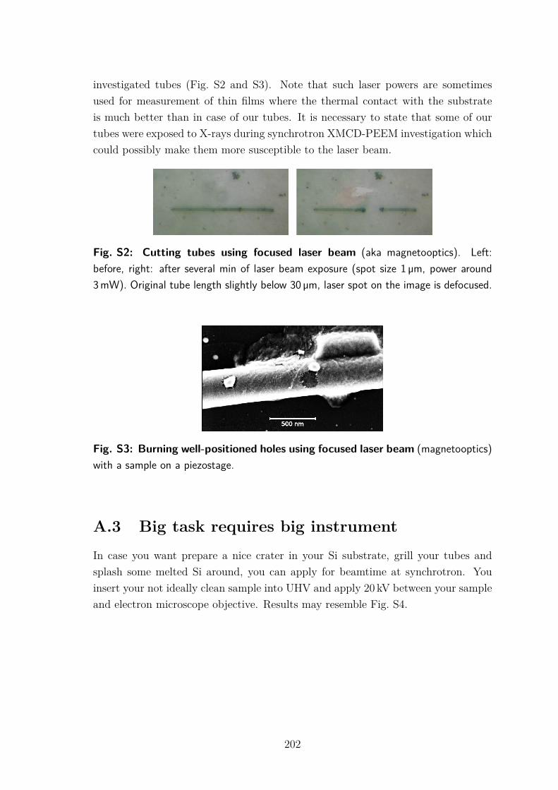
investigated tubes (Fig. S2 and S3). Note that such laser powers are sometimesused for measurement of thin films where the thermal contact with the substrateis much better than in case of our tubes. It is necessary to state that some of ourtubes were exposed to X-rays during synchrotron XMCD-PEEM investigation whichcould possibly make them more susceptible to the laser beam.
Fig. S2: Cutting tubes using focused laser beam (aka magnetooptics). Left:before, right: after several min of laser beam exposure (spot size 1 µm, power around3 mW). Original tube length slightly below 30 µm, laser spot on the image is defocused.
Fig. S3: Burning well-positioned holes using focused laser beam (magnetooptics)with a sample on a piezostage.
A.3 Big task requires big instrument
In case you want prepare a nice crater in your Si substrate, grill your tubes andsplash some melted Si around, you can apply for beamtime at synchrotron. Youinsert your not ideally clean sample into UHV and apply 20 kV between your sampleand electron microscope objective. Results may resemble Fig. S4.
202

(a) Sample overview (b) Detail of a tube
Fig. S4: Sample affected by electric discharge during XMCD-PEEM measure-ment. (a) Overview image with a crater in the Si substrate, (b) detail of a partiallymelted tube.
203

B ELECTRON HOLOGRAPHY
B.1 Electrostatic interaction constant c𝐸
In vacuum we express the electron velocity as
𝑣 = 𝑝c𝐸
c = 𝑝c𝐸k + 𝐸0
c, (B.1)
with electron momentum 𝑝 = 1c
√𝐸2
k + 2𝐸k𝐸0, c the speed of light in vacuum,𝐸 the total electron energy involving kinetic energy 𝐸k and rest energy 𝐸0 = m0c2,where m0 represents the rest mass of the electron.
Then inserting (B.1) into c𝐸 definition we obtain:
c𝐸 = e~
1𝑣
= e~
𝐸k + 𝐸0√𝐸2
k + 2𝐸k𝐸0
1c = 2𝜋e
h
√𝐸2
k + 2𝐸k𝐸0
c(𝐸k + 𝐸0)
𝐸2k + 2𝐸k𝐸0
= 2𝜋e𝑝
h(𝐸k + 𝐸0)
𝐸2k + 2𝐸k𝐸0
.
(B.2)Here we got rid of the square root in the denominator, using 𝑝 = 1
c
√𝐸2
k + 2𝐸k𝐸0
and h = 2𝜋~. If we recall the de Broglie wavelength (of the electron):
𝜆 = h𝑝
, (B.3)
with 𝜆 = h𝑝
(h is the Planck constant and 𝑝 the electron momentum), we can getexpression which is used in literature on electron holography [227]:
c𝐸 = 2𝜋e𝜆
(𝐸k + 𝐸0)𝐸2
k + 2𝐸k𝐸0. (B.4)
Note that in some (review) articles on electron holography - e.g. Kasama [188]and McCartney [189] (but also many others), the expression (B.4) is given withoutelementary charge e. But without this constant the expression makes no sense, asboth dimensions and order of magnitude are incorrect and inconsistent with valuesand dimension of the c𝐸, even with value+dimension provided in these articles justone line below the formula - e.g. [188]. Midgley’s review [227] provides the correctexpression including elementary charge.
The formula without e works only when energies are expressed as voltages, i.e.𝐸/e, this might be convenient in practical use as one just puts there acceleratingvoltage instead of energy (e.g. 300 kV) and 511 kV instead of electron rest energy𝐸0.
Now we will consider the value of c𝐸 for electron energy of 300 keV used in ourelectron holography experiments at CEMES Toulouse.
The relativistic relation between energy and momentum is:
𝐸2 = (𝐸k + 𝐸0)2 = 𝑝2c2 + m20c4. (B.5)
204
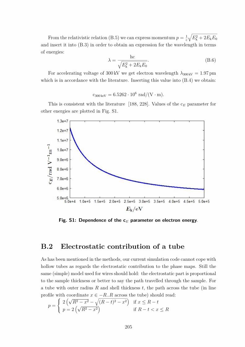
From the relativistic relation (B.5) we can express momentum 𝑝 = 1c
√𝐸2
k + 2𝐸k𝐸0
and insert it into (B.3) in order to obtain an expression for the wavelength in termsof energies:
𝜆 = hc√𝐸2
k + 2𝐸k𝐸0. (B.6)
For accelerating voltage of 300 kV we get electron wavelength 𝜆300 kV = 1.97 pmwhich is in accordance with the literature. Inserting this value into (B.4) we obtain:
c300 keV = 6.5262 · 106 rad/(V · m).
This is consistent with the literature [188, 228]. Values of the c𝐸 parameter forother energies are plotted in Fig. S1.
Fig. S1: Dependence of the c𝐸 parameter on electron energy.
B.2 Electrostatic contribution of a tube
As has been mentioned in the methods, our current simulation code cannot cope withhollow tubes as regards the electrostatic contribution to the phase maps. Still thesame (simple) model used for wires should hold: the electrostatic part is proportionalto the sample thickness or better to say the path travelled through the sample. Fora tube with outer radius 𝑅 and shell thickness 𝑡, the path across the tube (in lineprofile with coordinate 𝑥 ∈ −𝑅..𝑅 across the tube) should read:
𝑝 =⎧⎨⎩ 2
(√𝑅2 − 𝑥2 −
√(𝑅 − 𝑡)2 − 𝑥2
)if 𝑥 ≤ 𝑅 − 𝑡
𝑝 = 2(√
𝑅2 − 𝑥2)
if 𝑅 − 𝑡 < 𝑥 ≤ 𝑅
205
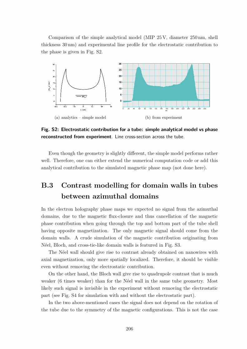
Comparison of the simple analytical model (MIP 25 V, diameter 250 nm, shellthickness 30 nm) and experimental line profile for the electrostatic contribution tothe phase is given in Fig. S2.
(a) analytics – simple model (b) from experiment
Fig. S2: Electrostatic contribution for a tube: simple analytical model vs phasereconstructed from experiment. Line cross-section across the tube.
Even though the geometry is slightly different, the simple model performs ratherwell. Therefore, one can either extend the numerical computation code or add thisanalytical contribution to the simulated magnetic phase map (not done here).
B.3 Contrast modelling for domain walls in tubesbetween azimuthal domains
In the electron holography phase maps we expected no signal from the azimuthaldomains, due to the magnetic flux-closure and thus cancellation of the magneticphase contribution when going through the top and bottom part of the tube shellhaving opposite magnetization. The only magnetic signal should come from thedomain walls. A crude simulation of the magnetic contribution originating fromNéel, Bloch, and cross-tie-like domain walls is featured in Fig. S3.
The Néel wall should give rise to contrast already obtained on nanowires withaxial magnetization, only more spatially localized. Therefore, it should be visibleeven without removing the electrostatic contribution.
On the other hand, the Bloch wall give rise to quadrupole contrast that is muchweaker (6 times weaker) than for the Néel wall in the same tube geometry. Mostlikely such signal is invisible in the experiment without removing the electrostaticpart (see Fig. S4 for simulation with and without the electrostatic part).
In the two above-mentioned cases the signal does not depend on the rotation ofthe tube due to the symmetry of the magnetic configurations. This is not the case
206

Tube
Bloch
Wall
50 nm
Neel
Wall
Cro
ss-t
ieW
all
Tub
e
Tub
e
250 nm 250 nm
Fig. S3: Crude electron holography simulations of the magnetic phase maps(no electrostatic contribution) for Bloch, Néel and cross-tie walls in between2 opposite azimuthal domains in a tube. Note that the Bloch wall was prepared in asmaller tube and the contrast range is different as well (for the same geometry, the Blochwall gives 6 times weaker contrast than the Néel one).
50 nm
(a) electrostatic only (b) electrostatic+magnetic (c) electrostatic+magnetic
Fig. S4: Simulation of electron holography phase map with electrostatic contri-bution for Bloch wall (radial magnetization) in between 2 opposite azimuthal domainsin a tube (for magnetic part only see in Fig. S3a). (a) Electrostatic part only. The high-est phase shift is close to tube edges where the electron path travelled through the tubeis the longest; the spatial extent corresponds roughly to the tube wall (shell) thickness.(b) and (c) depict both electrostatic and magnetic parts scaled to (a) full range of thephase, (b) small range around zero. The electrostatic part dominates and in experimentone cannot probably clearly see the weak magnetic signal without removing the electro-static contribution. Even here it is almost impossible to spot a small difference between(a) and (b).
for the cross-tie wall. In addition, here the contrast may depend on the numberof vortex-antivortex pairs (here 4, smaller amount is found in tubes with smaller
207
diameter).
B.4 Electron holography on NiCo nanowires withmodulated diameter
We consider here diameter-modulated Ni60Co40 nanowires. These have been intro-duced in the short tutorial about electron holography imaging – section 5.4.4. Weintend to use the investigation of diameter-modulated nanowires as a step towardsperforming similar measurements on tubes, later also with modulated-diameter.
In the ground state, such nanowires are axially magnetized (aside from curlingat the wire ends and diameter modulations). A typical nanowire geometry with di-ameter modulations has been already shown in Fig. 5.10. Two types of domain walls(DWs) may exist in such nanowires: transverse or Bloch point wall (see Fig. 2.4).We remind the readed that the diameter modulation is intended for easier nucleationand trapping of a DW in the thin section of the wire. After few initial trials, weperformed most of the experiments on one nanowire displayed in Fig. S5. This wirehas around 120 nm in diameter in the central thin section. Later, we probed otherNiCo nanowires, where we could nucleate even multiple DWs.
B.4.1 Domain wall nucleation and displacement
After applying an out-of-plane field pulse of 1 T (width of few s) with a slight tilt(around -8 ∘), we successfully nucleated a DW, which was located at the P1 site (seelocation in Fig. 5.10). Then, applying smaller fields of 30 mT (out-of-plane, alongthe beam) with different component along wire given by the sample tilt, we wereable to move the DW to P2 and then repeatedly with the same field (tilt) valuesbetween pinning sites P2 (tilt during field application: -18 ∘) and P3 (tilt duringfield application: +9 ∘. Therefore, there is a small component along the wire, butthe field has significant component transverse to the wire axis. An example of theDW pinned at P3 site is given in Fig. S6. As the initial sample needed for DWnucleation was -8 ∘ and when going above or below the tilt, the magnetization wasswitched we assume that the wire is initially already slightly tilted and at -8 ∘ thewire is perpendicular to the beam. In such case the both tilts for DW displacementcorresponds to approx. 10 ∘, which result in 5 mT applied along the wire axis (but30 mT total magnitude).
When we tried to reach again the P1 site, we gradually increased the sampletilt while keeping constant excitation of the objective lenses (producing still 30 mT).After the depinning, the DW went through the smooth diameter modulation and
208

P1
P3
P2
biprism Pt wire
CoNi nanowire
(below the sample)
P1-P3: DW pinning sites
Fig. S5: TEM image of the NiCo nanowire sample with pinning sites (P1-P3) for a domain wall. A magnetic domain wall was repeatedly nucleated at P1 siteand then moved back and forth many times between pinning sites P2 and P3. Insetsshow higher magnification images of the regions of interest (pinning sites, diametermodulation).
Fig. S6: Electron holography phase map (both magnetic and electrostatic part)of the nanowire with a domain wall (P3 site). The DW location is in between regionswith the contour lines concentrated on opposite sides of the wire – recall Fig. 5.12 fromour small electron holography tutorial. The position is also indicated by the stray field(outside the wire). It is not easy to determine the domain wall configuration just fromthe map itself.
209

then annihilated at the left wire end (complete magnetization reversal). With thesame field sequence as at the beginning we re-nucleated the DW at P1 and shifted itagain many times between P2 and P3 sites. Unfortunately, the diameter modulationswere not very efficient in trapping the DW except for the smooth modulation. Herethe DW was trapped rather due to a small notch (structural defect, see Fig. S7a) thanthe diameter change. In general, the DW pinning was stronger at local defects likea triangular grain at P3 site from Fig. S5. Therefore, after applying sufficiently highfield to depin the DW, the wall moved either to another local defect, or went throughthe diameter modulation and annihilated. This might be improved by enhancingthe material quality (lowering strength of natural pinning sites, e.g. by annealing)and changing the modulation geometry (more abrupt change in diameter).
(a) Smooth diameter modulation (b) Sharp diameter modulation
Fig. S7: NiCo nanowire – diameter modulations with a structural defect atthe smooth modulation. Scanning electron microscopy with backscattered electrondetection. The thicker wire part appear brighter, whereas the defects – notches (missingmaterial) are dark in the image – this is the P1 area.
B.4.2 Domain wall identification
While localization of the DW position is easy, the determination of its type andmagnetic configuration can be difficult. We did numerical modelling of nanowireswith both TW and BPW for comparison with the experimental images. The electronphase shift maps for the wire with a DW and their numerical modelling are summa-rized in Fig. S8. The electrostatic part which may make the DW identification moredifficult can be either removed experimentally or included in the simulations. Thefirst option paves the way towards quantitative matching of the DW pattern but it istime consuming from the experimental point of view. On the other hand, even witha rather simple model for the electrostatic part we can reproduce the experimentnumerically without this nuisance. The experimental magnetic phase shift is slightlysmaller than in the simulations; we attribute this to a reduced path-integrated mag-netic induction due to surface oxidation. Quantitative agreement for both magneticand electrostatic contributions is possible yet difficult due to the model simplicity
210

(a) (b) (c)
(d) (e) (f)
Fig. S8: Electron holography – experiment (top) vs simulations (bottom). (a)hologram (wire+interference fringes); experimental phase maps: (b) magnetic only and(c) electrostatic+magnetic. Simulated phase: (d) electrostatic only, (e) magnetic onlyand (f) both contributions with a scheme of the magnetization pattern. Here the az-imuth of the core of the transverse wall is in-between in-plane and out-of-plane (beam)direction. There is a curling with opposite sense of circulation on either side of the walldue to the large wire diameter (120 nm).
and electrostatic contributions arising from an inhomogeneous supporting carbonfilm, defects and crust of impurities on the wire (Fig. S8a).
In all our experiments so far, we identified the transverse wall with variousorientation (azimuth). Fig. S9 and Fig. S10 show that depending on this azimuth,the same DW type (TW) produces different magnetic phase maps.
The question arises, whether one is able to unambiguously distinguish a BPWfrom a TW with an a priori unknown azimuth. The more challenging case is whenthe azimuth of the TW is aligned with the electron beam direction as the phase isnot sensitive to the magnetic induction pointing along the beam. Even in this casewe can distinguish a BWP and from a TW thanks to an additional curling that hasopposite sense at either side of the TW – this has been already reported in [14]. Forthe BPW the curling sense is the same on both sides of the wall. Note that differentmagnetic configurations can produce very similar phase maps, e.g. BPW and idealTW without curling pointing along the beam (exist only for small diameters [15] –not our case). Therefore, ideally one should acquire images for at least a few tiltsto avoid the misinterpretation.
In few cases we were in doubt regarding distinguishing BPW and TW. Therefore,we performed imaging with tilted sample – always ±tilt (e.g. ±𝑋 ∘). This shouldgive us some information on the out-of-plane magnetic induction. The phase mapsfor BPW should look the same (at least the magnetic part) when tilting the samplealong the wire axis (rotating the wire), just due to the BPW symmetry. Tilting thewire with respect to the axis perpendicular to the wire could also allow to deter-mine the curling sense. In all cases transverse wall with various core magnetization
211

Experiment
150 nm
Simulation: TW -120◦ from z
z
x
y
Fig. S9: Magnetic phase maps for a transverse domain wall: experiment (top,diameter ) vs simulation (bottom). Dashed lines show the approximate wire position.
Bloch Point Wall Transverse Wall along +x
Transverse Wall along −z
z
x
y
Transverse Wall -120◦ from z
Fig. S10: Simulated magnetic phase maps for Bloch point wall and transversewall with different azimuths (orientations) for the latter. The transverse wall cangive rise to very different phase maps depending on the magnetization direction in thedomain wall core. Similar effect may also happen if the angle between the wire and theelectron beam changes (tilted sample). Dashed lines show the approximate wire extent.
212
orientation was found.
B.4.3 Summary of electron holography on modulated nano-wires
In case of CoNi nanowires, the magnetic signal related to opposite axial magnetiza-tion was distinguishable even without removing the electrostatic contribution. Thestray field was observed emanating both from diameter modulation (Fig. 5.12) aswell as from a DW (Fig. S6). Electron holography together with simulations enablesidentification of the type of DW and determination of its structure. Our simulationsof the electron holography phase maps shows very good agreement with the experi-ment (Fig. S8). Both magnetic and electrostatic contributions to the phase shift canbe modelled and even simple electrostatic model (phase proportional to thicknesstimes constant MIP) gives satisfactory results. We evidenced the transverse wallwith the orientation of the transverse magnetization sometimes changed after thewall displacement with the magnetic field.
We were able to reproduce nucleation, shifting (back and forth among severalpinning sites) and annihilation of the DW. The diameter modulations were notefficient in stopping the domain wall – the wall was pinned rather on local defect (e.g.notches). Better material quality and more abrupt diameter change are required.Different approach can be followed as well – e.g. with segments from differentmaterials [26] or tube-wire elements discussed in the min text.
We benefited from the experience and familiarity with the technique in fur-ther investigation of magnetic tubes. In future, we hope to apply similar samplepreparation, domain wall nucleation and manipulation also to diameter modulatednanotubes.
213

C FEELLGOOD – MAGNETIC STATE INITIAL-IZATION
Below we give an example of a script used for building initial magnetic configurationfor FeeLLGood micromagnetic simulations. In this particular case it is state withtwo azimuthal domains having opposite circulation of magnetization, separated byan ideal Bloch-like domain wall (radial magnetization).
# include "fem.h"
// Initial distribution of magnetization// tube along z, with z=0 being its centre// 2 azimuthal domains separated by a Bloch -like domain wall
void init_distrib (Fem &fem){const int NOD = fem.NOD;int chir; // auxiliary for sense of azimuthal curling
for (int i=0; i<NOD; i++){Node &node = fem.node[i];double x = 2.*( node.x-fem.cx)/ fem.lx; // x in -1..1]double y = 2.*( node.y-fem.cy)/ fem.ly; // y in -1..1]double z = 2.*( node.z-fem.cz)/ fem.lz; // z in -1..1]double a=0.1; // initial extent of the wall along zdouble u0 , u1 , u2; // auxiliary for M_x , M_y , M_zdouble teta=atan2(y,x);
// define opposite chirality for the 2 azimuthal domainsif (z >0) {chir =1;}else {chir = -1;}
// radial magnetization in the wall (i.e. around z=0)if (abs(z)<a {
u0 = x; // M_xu1 = y; // M_yu2 = 0; // M_z
}// azimuthal magnetization in the domains
214
else {u0 = ( -1)* chir*sin(teta ); // M_xu1 = chir*cos(teta ); // M_yu2 = 0; // M_z
}
// norm for normalization of the magnetization vectordouble norme=sqrt(u0*u0+u1*u1+u2*u2);
// asign normalized magnetization vector to nodesnode.u[0] = u0/norme;node.u[1] = u1/norme;node.u[2] = u2/norme;node.phi = 0;} // end for
} //
215

D INTRODUCTION (FRANÇAIS)
La recherche en magnétisme aux petites dimensions (le micro et nanomagnétisme) aaccompagné la révolution dans le stockage de données de capacité toujours croissante(par ex. disques durs, HDD), de nouveaux capteurs magnétiques (pour des besoinsd’orientation, de mesure de rotation et vitesse). Ceci s’est fait en se concentrantprincipalement sur les films minces, les nanoparticules et plus récemment nanofils.
En 2004, S. Parkin de IBM [1] a proposé un concept de mémoire à l’état solidenon volatile (Mémoire racetrack, Fig. 1.1) basé sur l’existence et le déplacementde parois de domaines magnétiques (DW) dans des nanopistes [2]. Une telle mé-moire serait rapide, robuste (non sensible aux coupures de courant, sans mouvementmécanique de pièces), avec une consommation d’énergie modérée et dans le cas degrands réseaux de pistes verticales, la perspective de densité de stockage élevée.
Récemment, d’autres types de mémoires tendent à exploiter la troisième dimen-sion (par exemple la mémoire flash, consistant maintenant en quelques dizaines decouches empilées). Des tentatives existent pour les disques dur avec quelques (2-3)couches d’enregistrement, qui pourraient bientôt arriver sur le marché. Cependant,la mémoire racetrack reste encore dans les laboratoires, voire simplement un con-cept. En effet, IBM et de nombreux autres groupes ont apporté la preuve de conceptracetrack sur la base de bandes magnétiques planaires réalisées par lithographie, etont contribué à la compréhension fondamentale du déplacement de parois de do-maine. Cependant, même dans un article récent [5], S. Parkin admet qu’aller en 3Dest un défi considérable, principalement du point de vue de la fabrication.
Plus récemment, des études ont été menées sur des nanofils cylindriques pré-parés par des méthodes (électro)chimiques [6]. Au-delà des nanofils cylindriques,il est maintenant évoqué d’autres géométries incurvées (l’étude de l’interaction decourbure et du magnétisme) [7] ainsi que des nano-aimants en 3D (nanomagnétismetridimensionnel) [8]. Il s’agit pour l’instant essentiellement de propositions et con-cepts, avec très peu de réalisations expérimentales, même sous forme d’ébauches.Ces deux aspects (Fig. 1.2) possèdent des recouvrement et apportent de nouveauxdéfis, promettant de nouvelles configurations magnétiques, de la physique, et possi-blement une plus grande densité surfacique de composants dans les dispositifs.
Nanofils et nanotubes magnétiques
En nanomagnétisme et spintronique, le déplacement de parois de domaines mag-nétiques a été principalement étudié en bandes planaires préparées par lithogra-phie [5, 10]. Cependant, les nanotubes (NT) et nanofils cylindriques (NWs) fabriqués
216
sous forme de réseaux verticaux par des méthodes dites bottom-up, sont plus appro-priés pour la conception de dispositifs de stockage à haute densité avec l’architecture3D en termes de synthèse de structures très profondes.
Dix ans après la proposition initiale de mémoire racetrack, l’attention est passéedes expériences sur des réseaux étendues de nanofils cylindriques, à la physique dunanofil isolé. Cette dernière a été abordée par le transport électronique [11], la mag-nétométrie [12], et l’imagerie magnétique [13] apportant les premières confirmationsexpérimentales de parois de domaines spécifiques aux nanofils cylindriques [14, 15].Ces nanofils pourraient fournir un système modèle pour l’étude du déplacement deparois sous champ magnétique [16] ou sous un courant polarisé en spin [17], avecnotamment une vitesse très rapide prédite (> 1 km/s) [17]. Cependant, les paroisdans les nanofils magnétiquement doux sont de type tête-à-tête ou queue-à-queueen raison de l’aimantation axiale dans les domaines. Ces parois sont intrinsèque-ment associées à une importante charge monopolaire magnétostatique. Le champde fuite à longue portée qui en résulte pourrait induire des interactions indésirables(couplages entre parois et entre fils) dans le cas de réseaux denses. Une solutionpour contourner ce problème repose sur des matériaux artificiels, appelés matériauxantiferromagnétiques synthétiques et qui ne génèrent pas de champ de fuite. Mais,alors que le concept a été démontré pour les nanostructures 2D et est utilisé dansles dispositifs commerciaux [5], l’implémentation 3D n’a pas encore été réalisée pourdes raisons de difficulté de synthèse.
Les nanotubes magnétiques, moins étudiés que la simple géométrie des nanofils,ont été rapportés principalement dans le cadre de la biomédecine [18] et de la catal-yse [19]. Cependant, leurs propriétés magnétiques individuelles restent largementméconnues. Pourtant, la théorie et les simulations prédisent une physique similairedes nanotubes, par rapport aux nanofils cylindriques [20, 21], y compris un mouve-ment de parois rapide (> 1 km/s) sans instabilité de Walker [22]. De plus, en termesde nouvelle physique et de nouveaux dispositifs, les nanotubes semblent être plusappropriés que les nanofils solides. En effet, leurs propriétés magnétiques pourraientêtre ajustées en modifiant l’épaisseur de la coquille du tube, et des architectures pluscomplexes peuvent être élaborées à partir de structures cœur-coquille [23]. Ceux-cisont analogues aux multicouches en spintronique 2D (spin-electronics), comme lescouches magnétiques séparées par une fin intercalaire non magnétique pour obtenirdes effets de magnétorésistance [9], des antiferromagnétiques synthétiques, du cou-plage d’échange etc.
En outre, comme cela a déjà été fait pour les nanofils [24–26], on peut ajusterles propriétés magnétiques et la fonctionnalité des dispositifs potentiels en modifiantles propriétés le long des tubes (les modifications pourraient également être utiliséespour la définition des bits dans la mémoire racetrack):
217

• matériau: composition, segments de différents éléments [27], dopage, irradia-tion ...
• changement géométrique: modulation de diamètre sous forme de protrusions,ou constrictions [28], entailles-défauts, éléments tube-fils (avec des segmentsde fils et tubes) [29, 30]
• structures cœur-coquille [23] / multicouches [31].
Pourquoi les nanotubes magnétiques?
Dans ce travail, nous nous intéressons uniquement aux propriétés magnétiques etaux applications possibles des nanotubes en spintronique. En dehors de ceux-ci,les tubes ont d’autres propriétés intéressantes pour différents domaines, par ex.grande surface – utile pour la catalyse. Par ailleurs, les surfaces interne et externepeuvent être fonctionnalisées et/ou des molécules peuvent être stockées à l’intérieurdu tube. Les nanotubes magnétiques peuvent apporter des phénomènes nouveauxou améliorés en raison de leur géométrie, une topologie différente par rapport auxfilms plans, et la possibilité de créer des structures et des dispositifs plus complexesà base de nanotubes multicouches (Fig. 1.3).
Les tubes apportent une autre possibilité radicalement nouvelle: la courburequi leur est associée a été prédite comme conduisant à la brisure de la symétried’inversion, liée au fait que les surfaces interne et externe sont distinctes. Cela nese produit pas pour un film plat parfait, mais seulement pour les multicouches –couche magnétique prise en sandwich entre deux couches différentes (non magné-tiques). Par conséquent, à cet égard, un tube magnétique (surface courbe) apportela fonctionnalité de certaines hétérostructures en couches minces. Dans les sys-tèmes plans comme les films Pt/Co/AlO𝑥 (avec une couches de Co ultramince etdonc une aimantation perpendiculaire), la brisure de la symétrie d’inversion est as-sociée à la promotion des textures magnétiques chirales, à la propagation rapidedes parois de domaines magnétiques [32] et à la non-réciprocité de propagation desondes de spin [33]. Des phénomènes similaires devraient en effet se produire dansle cas de nanotubes magnétiques (couche magnétique unique, aucune couche sup-plémentaire nécessaire): la courbure induit la magnétochiralité [34], l’anisotropies’apparantant à une interaction dite Dzyaloshinskii-Moriya [7]. Récemment, desprédictions théoriques de la non-réciprocité de la propagation des ondes de spindans les tubes ont été faites [35, 36].
Une question ouverte et passionnante est de savoir si l’on pourrait combiner deseffets provenant à la fois de la courbure et des interfaces avec différents matéri-aux et rendre les effets (par exemple, l’interaction Dzyaloshinskii-Moriya) encore
218

plus forts. La combinaison de telles structures cœur-coquilles avec modification despropriétés le long des structures comme indiqué ci-dessus (par exemple matériau,géométrie) pourrait conduire a par exemple, de nouveaux guides d’ondes magnon-iques (ondes de spin). Certaines structures cœur-coquilles ont déjà été réalisés, parexemple des vannes de spin [37]. Cependant, la plupart des empilement pertinentsn’a pas encore été synthétisée: les matériaux antiferromagnétiques synthétiques, lesstructures à métaux lourds (Pt) exploitant l’effet Hall de spin [38, 39] et l’interactionDzyaloshinskii-Moriya [40] . . . Au-delà de la physique nouvelle, des réseaux verticauxde tels nanotubes multicouches pourraient permettre le transfert de la spintronique2D vers la 3D et rendre ainsi les dispositifs spintroniques plus compétitifs.
Les chimistes et les spécialistes des matériaux savent fabriquer une grande var-iété de nanostructures à partir de différents matériaux et de différentes formes ycompris les nanotubes magnétiques, les tubes multicouches et les nanofils cœur-coquilles. Cependant, la caractérisation de telles structures est très souvent faite pardes mesures globales, typiquement par magnétométrie sur des réseaux ou faisceauxde telles structures. D’un autre côté, les physiciens peuvent imager et mesurer desnanostructures isolées, mais jusqu’à présent, ils se sont concentrés principalementsur des éléments en couches minces préparées par lithographie, qui leur est un outilhabituel. Dans ce travail, nous bénéficions de ces deux mondes. L’auteur lui-mêmeest un hybride d’ingénieur, de physicien et de chimiste. Nous profitons égalementd’une collaboration avec des chimistes experts et des spécialistes des matériaux del’Université de Darmstadt, en particulier Sandra Schaefer.
Organisation du manuscrit
Le manuscrit présenté comporte 4 parties:• I: Théorie et état de l’art• II: Méthodes et instrumentation• III: Résultats et discussion – Nanotubes magnétiques• IV: Résultats et discussion – Nanotubes multicouchesNous commencerons donc par un examen de l’historique théorique et des infor-
mations de ce qui a déjà été fait dans le domaine des nanostructures magnétiquesallongées, et en particulier des nanotubes. La partie II décrit les techniques que nousavons utilisées dans nos études, ainsi que certaines informations connexes. Enfin, lesrésultats (les expériences et modélisation numérique) sont abordés dans les partiesIII et IV; la partie III se concentre sur les nanotubes magnétiques et la dernière surdes structures cœur-coquilles plus avancées (tubes multicouches).
219
E CONCLUSION (FRANÇAIS)
Nous avons fabriqué avec succès des nanotubes à partir de plusieurs matériaux fer-romagnétiques par des méthodes électrochimiques dans des gabarits nanoporeux. Asavoir, nous avons préparé des nanotubes de NiCo (diamètre 70-90 nm), des nan-otubes de Ni (diamètre aux environs de 60 nm) et des nanostructures avec des seg-ments alternés sous forme de fil (plein) et de tube (creux). De plus, nous avonsobtenu des tubes par dépôt autocatalytique: CoNiB et NiFeB (diamètres 80-400 nm)ainsi que des tubes multicouches de nos collaborateurs de TU Darmstadt. En plusde ceux-ci, nous avons fabriqué nous-mêmes des nanotubes CoNiB, par la mêmetechnique (diamètres 100-200 nm).
Nous avons étudié toutes ces nanostructures à l’aide de la microscopie électron-ique (à balayage / en transmission) et, dans certains cas, de la microscopie à forceatomique. En plus de l’étude de la morphologie et de la topographie, nous avonseffectué une analyse chimique en utilisant la spectroscopie à rayons X à dispersiond’énergie. De plus, nous avons quelques analyses chimiques préliminaires de nos col-laborateurs (CEMES, Toulouse et Spintec, Grenoble) par la spectroscopie de perted’énergie des électrons. L’étude magnétique, aspect clé de ce travail, a été menéeavec une combinaison de diverses microscopies magnétiques: l’holographie électron-ique, la microscopie à force magnétique, et surtout les microscopies de dichroïsmecirculaire magnétique de rayons X associé à la microscopie à émission de photo-electrons (XMCD-PEEM) ou microscopie à rayons X en transmission à balayage(STXM). Ceux-ci ont été complétés par la magnétométrie sur des réseaux de tubeset sur des structures isolées. Nos résultats sont étayeés par des simulations micro-magnétiques et la modélisation numérique d’images XMCD-PEEM.
Tubes CoNiB et NiFeB déposés par voie chimique
Dans les tubes CoNiB préparés par dépôt autocatalytique (diamètre autour de300 nm), l’imagerie XMCD-PEEM et la comparaison avec la modélisation numériqueont révélé des séries de domaines magnétiques bien définis avec aimantation azimu-tale, séparés par des parois de domaines de type Bloch (aimantation radiale). Cesdomaines à fermeture de flux magnétique génèrent des champs de fuite faibles et àcourte distance, tout en étant séparés par des parois étroites, significativement plusétroites que le diamètre du tube. La densité de parois de domaine peut atteindre5/µm. Si l’on ne tenait compte que de la géométrie, ces tubes longs (jusqu’à 30 µmde longueur) devraient être aimantés axialement. Ainsi, une contribution supplé-mentaire de l’anisotropie magnétique doit être présente afin de favoriser l’alignementde l’aimantation le long de la direction azimutale (c’est-à-dire l’axe facile pour l’axe
220
azimutal et l’axe difficile pour la direction longitudinale). L’anisotropie azimutalepourrait provenir de la déformation induite par la croissance et / ou de la forme dugrain (microstructure). Nous ne pouvons pas non plus exclure l’effet de la dissolutionrapide du gabarit.
Lorsqu’un champ magnétique est appliqué le long de l’axe du tube, l’aimantationtourne progressivement vers la direction axiale. Grâce à l’imagerie STXM sous untel champ, nous avons pu extraire la force de l’anisotropie, correspondant à une con-stante d’anisotropie effective d’environ de 10 kJ/m3. La valeur de l’anisotropie a puêtre adaptée par recuit ou variation de la composition du matériau. En particulier,après recuit à environ 450 ∘C, l’aimantation est axiale et peut être renversée avecplusieurs mT appliquées le long de l’axe du tube.
Les tubes NiFeB de géométrie similaire préparés de la même manière sont aiman-tés axialement même sans traitement (comme recuit effectué pour les tubes CoNiB).Contrairement à CoNiB (magnétostriction négative significative), NiFeB présenteune magnétostriction presque nulle (faiblement positive). Sur cette base, nous met-tons en avant l’origine magnétoélastique des domaines azimutaux dans les tubesCoNiB. Nous avons observé le renversement d’aimantation des tubes NiFeB sous unchamp magnétique et le déplacement d’une paroi de domaine. Dans les expériencesd’holographie électronique, nous avons observé des cartes de phase complexes quenous attribuons à un grand diamètre de tube (parfois près de 400 nm) et à un champayant une composante transversale significative par rapport à l’axe du tube.
Une autre façon d’obtenir une aimantation axiale est de réduire le diamètre.Les nanotubes de CoNiB d’un diamètre d’environ 100 nm montrent une aimanta-tion longitudinale, à la fois en XMCD-PEEM et en imagerie par microscopie à forcemagnétique. Même s’il peut y avoir une certaine anisotropie azimutale, l’énergied’échange associée à l’aimantation azimutale serait trop élevée et donc une aiman-tation axiale est préférée.
Certains nanotubes, principalement préparées par dépôt électrolytique (NiCo,Ni) avec des parois minces (< 15 nm), n’ont pas pu être étudiés correctement pardes microscopies magnétiques en raison du très faible signal résultant de l’oxydation(partielle) du matériau. De tels nanotubes minces devraient être encapsulés pardes couches protectrices, par ex. quelques nanomètres de silice / hafnia déposéspar dépôt par couche atomique (ALD), ou de l’oxyde de titane préparé par dépôtchimique en bain.
Outre la focalisation sur les nanotubes, nous avons également étudié des géométriesplus complexes: des nanoéléments avec des segments de fil et de tube et des tubesmulticouches (structures cœur-coquilles).
221

Nanostructures tube-fils
Les nanoéléments avec des segments composés de nanofils et nanotubes alternés (di-amètre extérieur d’environ 60 nm) présentaient des transitions tube/fil très nettes(des transitions progressives font l’essentiel des rapports de la littérature) avecplusieurs segments de tubes de longueur supérieure à 2 µm (plus long que dans la lit-térature). Malheureusement, la structure s’est avérée très difficile pour la premièreimagerie par microscopie magnétique. Un petit diamètre avec un moment magné-tique faible de Ni a donné un faible signal magnétique pour les parties de nanofils,sans parler des segments tubulaires, où nous n’avons pas pu conclure. Dans le cas duXMCD-PEEM (plus sensible), nous avons rencontré des problèmes de localisationde structures ainsi qu’une résolution spatiale limitée et une analyse d’image renduecomplexe en raison d’une forte courbure. Cependant, avec des structures légèrementplus grandes (plus épaisses) contenant Fe ou Co (moment magnétique plus élevé),on pourrait tester expérimentalement des prédictions numériques et théoriques con-cernant ces structures intrigantes combinant des segments de fils et de tubes.
Tubes multicouches (structures cœur-coquilles)
Pour les dispositifs potentiels (spintroniques, par exemple les capteurs), il faudraitutiliser des tubes multicouches (structures coeur coquilles), et pas seulement destubes simples. Dans cet objectif, en collaboration avec TU Darmstadt, nous avonspréparé des tubes multicouches avec deux couches magnétiques différentes séparéespar un intercalaire non magnétique (NiFeB / SnOx / CoNiB). Grâce à la sensibil-ité en élément du XMCD-PEEM, nous avons pu étudier séparément chaque couchemagnétique. Celles-ci ont été trouvées découplées du point de vue de l’interactiond’échange. L’anisotropie de chaque couche prédominait, donc le CoNiB présen-tait des domaines azimutaux, alors que l’aimantation axiale a été identifiée dans lacouche de NiFeB. En outre, nous avons sondé le renversement d’aimantation dansles tubes, par champ magnétique. Sous un champ magnétique quasistatique, nousavons observé le renversement de la couche NiFeB par nucléation et propagationd’une paroi de domaine; des changements sont apparus dans le CoNiB, mais ceux-cine pouvaient pas être clairement corrélés avec l’état de la couche de NiFeB, saufpour l’effet du champ de fuite émanant d’une paroi de domaine dans la couche deNiFeB. Des expériences avec des impulsions de champ se sont révélées instructives,lorsque le champ a été appliqué avec un certain angle par rapport à l’axe du tube.À notre grande surprise, non seulement la couche NiFeB a été renversée, mais aussila circulation de tous les domaines azimutaux de CoNiB a été inversée.
222
Mis à part les expériences, nous avons également effectué des simulations micro-magnétiques de tubes multicouches avec un espaceur plus épais (par exemple 10 nm).Ici, nous avons pu démontrer l’alignement antiparallèle des domaines aimantés ax-ialement dans les deux couches magnétiques par interaction dipolaire, ainsi quel’obtention de parois de domaines de type vortex couplées des dans les deux tubes.
En dépit du caractère préliminaire dans certains cas de nos résultats, nous pen-sons avoir montré la polyvalence des nanotubes magnétiques. En modifiant la com-position, la géométrie ou le recuit, il est possible d’obtenir des domaines presqueà la carte: azimutaux ou axiaux, les deux étant utiles. Les domaines azimutaux,en particulier, sont intéressants en raison de la fermeture de flux magnétique quipourrait être exploitée dans des capteurs magnétiques ou dans des dispositifs baséssur des réseaux d ’éléments denses. La nature creuse et les domaines azimutauxréduiraient significativement l’interaction entre ces éléments et les interférences in-désirables. Les propriétés et la viabilité des tubes peuvent être encore améliorées enpréparant des structures cœur-coquille / multicouches tubulaires.
Nous nous sommes focalisés sur des nanotubes magnétiques, des structures cylin-driques avec un coeur vide. La courbure et l’absence de matière sur l’axe donnentdes propriétés intéressantes qui pourraient être exploitées en spintronique 3D, que cesoit pour des mémoires à l’état solide, des capteurs avancés ou des cristaux magnon-iques pour les guides d’ondes de spin, le tout basé sur (des réseaux verticaux de)tubes multicouches ou des nanofils coeur coquille.
223