Low-impedance thin-film polycrystalline silicon microelectrodes for extracellular stimulation and...
11
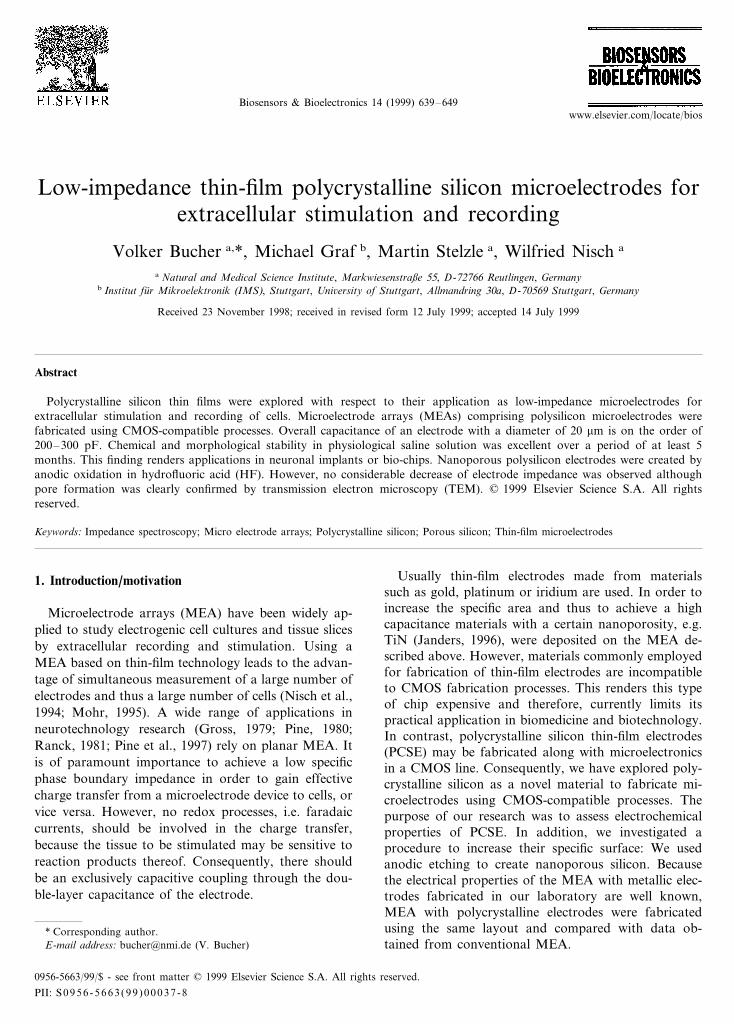
Biosensors & Bioelectronics 14 (1999) 639 – 649 Low-impedance thin-film polycrystalline silicon microelectrodes for extracellular stimulation and recording Volker Bucher a, *, Michael Graf b , Martin Stelzle a , Wilfried Nisch a a Natural and Medical Science Institute, Markwiesenstraße 55, D-72766 Reutlingen, Germany b Institut fu ¨r Mikroelektronik (IMS), Stuttgart, Uni6ersity of Stuttgart, Allmandring 30a, D-70569 Stuttgart, Germany Received 23 November 1998; received in revised form 12 July 1999; accepted 14 July 1999 Abstract Polycrystalline silicon thin films were explored with respect to their application as low-impedance microelectrodes for extracellular stimulation and recording of cells. Microelectrode arrays (MEAs) comprising polysilicon microelectrodes were fabricated using CMOS-compatible processes. Overall capacitance of an electrode with a diameter of 20 mm is on the order of 200 – 300 pF. Chemical and morphological stability in physiological saline solution was excellent over a period of at least 5 months. This finding renders applications in neuronal implants or bio-chips. Nanoporous polysilicon electrodes were created by anodic oxidation in hydrofluoric acid (HF). However, no considerable decrease of electrode impedance was observed although pore formation was clearly confirmed by transmission electron microscopy (TEM). © 1999 Elsevier Science S.A. All rights reserved. Keywords: Impedance spectroscopy; Micro electrode arrays; Polycrystalline silicon; Porous silicon; Thin-film microelectrodes www.elsevier.com/locate/bios 1. Introduction/motivation Microelectrode arrays (MEA) have been widely ap- plied to study electrogenic cell cultures and tissue slices by extracellular recording and stimulation. Using a MEA based on thin-film technology leads to the advan- tage of simultaneous measurement of a large number of electrodes and thus a large number of cells (Nisch et al., 1994; Mohr, 1995). A wide range of applications in neurotechnology research (Gross, 1979; Pine, 1980; Ranck, 1981; Pine et al., 1997) rely on planar MEA. It is of paramount importance to achieve a low specific phase boundary impedance in order to gain effective charge transfer from a microelectrode device to cells, or vice versa. However, no redox processes, i.e. faradaic currents, should be involved in the charge transfer, because the tissue to be stimulated may be sensitive to reaction products thereof. Consequently, there should be an exclusively capacitive coupling through the dou- ble-layer capacitance of the electrode. Usually thin-film electrodes made from materials such as gold, platinum or iridium are used. In order to increase the specific area and thus to achieve a high capacitance materials with a certain nanoporosity, e.g. TiN (Janders, 1996), were deposited on the MEA de- scribed above. However, materials commonly employed for fabrication of thin-film electrodes are incompatible to CMOS fabrication processes. This renders this type of chip expensive and therefore, currently limits its practical application in biomedicine and biotechnology. In contrast, polycrystalline silicon thin-film electrodes (PCSE) may be fabricated along with microelectronics in a CMOS line. Consequently, we have explored poly- crystalline silicon as a novel material to fabricate mi- croelectrodes using CMOS-compatible processes. The purpose of our research was to assess electrochemical properties of PCSE. In addition, we investigated a procedure to increase their specific surface: We used anodic etching to create nanoporous silicon. Because the electrical properties of the MEA with metallic elec- trodes fabricated in our laboratory are well known, MEA with polycrystalline electrodes were fabricated using the same layout and compared with data ob- tained from conventional MEA. * Corresponding author. E-mail address: [email protected] (V. Bucher) 0956-5663/99/$ - see front matter © 1999 Elsevier Science S.A. All rights reserved. PII:S0956-5663(99)00037-8
-
Upload
independent -
Category
Documents
-
view
0 -
download
0
Transcript of Low-impedance thin-film polycrystalline silicon microelectrodes for extracellular stimulation and...
Biosensors & Bioelectronics 14 (1999) 639–649
Low-impedance thin-film polycrystalline silicon microelectrodes forextracellular stimulation and recording
Volker Bucher a,*, Michael Graf b, Martin Stelzle a, Wilfried Nisch a
a Natural and Medical Science Institute, Markwiesenstraße 55, D-72766 Reutlingen, Germanyb Institut fur Mikroelektronik (IMS), Stuttgart, Uni6ersity of Stuttgart, Allmandring 30a, D-70569 Stuttgart, Germany
Received 23 November 1998; received in revised form 12 July 1999; accepted 14 July 1999
Abstract
Polycrystalline silicon thin films were explored with respect to their application as low-impedance microelectrodes forextracellular stimulation and recording of cells. Microelectrode arrays (MEAs) comprising polysilicon microelectrodes werefabricated using CMOS-compatible processes. Overall capacitance of an electrode with a diameter of 20 mm is on the order of200–300 pF. Chemical and morphological stability in physiological saline solution was excellent over a period of at least 5months. This finding renders applications in neuronal implants or bio-chips. Nanoporous polysilicon electrodes were created byanodic oxidation in hydrofluoric acid (HF). However, no considerable decrease of electrode impedance was observed althoughpore formation was clearly confirmed by transmission electron microscopy (TEM). © 1999 Elsevier Science S.A. All rightsreserved.
Keywords: Impedance spectroscopy; Micro electrode arrays; Polycrystalline silicon; Porous silicon; Thin-film microelectrodes
www.elsevier.com/locate/bios
1. Introduction/motivation
Microelectrode arrays (MEA) have been widely ap-plied to study electrogenic cell cultures and tissue slicesby extracellular recording and stimulation. Using aMEA based on thin-film technology leads to the advan-tage of simultaneous measurement of a large number ofelectrodes and thus a large number of cells (Nisch et al.,1994; Mohr, 1995). A wide range of applications inneurotechnology research (Gross, 1979; Pine, 1980;Ranck, 1981; Pine et al., 1997) rely on planar MEA. Itis of paramount importance to achieve a low specificphase boundary impedance in order to gain effectivecharge transfer from a microelectrode device to cells, orvice versa. However, no redox processes, i.e. faradaiccurrents, should be involved in the charge transfer,because the tissue to be stimulated may be sensitive toreaction products thereof. Consequently, there shouldbe an exclusively capacitive coupling through the dou-ble-layer capacitance of the electrode.
Usually thin-film electrodes made from materialssuch as gold, platinum or iridium are used. In order toincrease the specific area and thus to achieve a highcapacitance materials with a certain nanoporosity, e.g.TiN (Janders, 1996), were deposited on the MEA de-scribed above. However, materials commonly employedfor fabrication of thin-film electrodes are incompatibleto CMOS fabrication processes. This renders this typeof chip expensive and therefore, currently limits itspractical application in biomedicine and biotechnology.In contrast, polycrystalline silicon thin-film electrodes(PCSE) may be fabricated along with microelectronicsin a CMOS line. Consequently, we have explored poly-crystalline silicon as a novel material to fabricate mi-croelectrodes using CMOS-compatible processes. Thepurpose of our research was to assess electrochemicalproperties of PCSE. In addition, we investigated aprocedure to increase their specific surface: We usedanodic etching to create nanoporous silicon. Becausethe electrical properties of the MEA with metallic elec-trodes fabricated in our laboratory are well known,MEA with polycrystalline electrodes were fabricatedusing the same layout and compared with data ob-tained from conventional MEA.
* Corresponding author.E-mail address: [email protected] (V. Bucher)
0956-5663/99/$ - see front matter © 1999 Elsevier Science S.A. All rights reserved.
PII: S 0 9 5 6 -5663 (99 )00037 -8
V. Bucher et al. / Biosensors & Bioelectronics 14 (1999) 639–649640
2. Methods
2.1. Substrates
Monocrystalline silicon wafers were used as sub-strates. A SiO2 layer of 1 mm thickness was deposited torealize an insulating substrate. Thus, the substrate isfully compatible with requirements of CMOS produc-tion lines.
2.2. Deposition of polycrystalline silicon
A thin film of polycrystalline silicon (500 nm) wasdeposited on the insulating oxide layer by plasma-en-hanced chemical vapor deposition (PECVD) at 620°Cand 300 mTorr according to:
SiH4�Si+2H2
Undoped polycrystalline layers show a high resis-
tance, therefore, the silicon layer was doped by ionimplantation with boron up to a final concentration of2×1019 cm−3 resulting in a specific resistance of 5mVcm. The polycrystalline silicon develops a passivat-ing layer of native oxide as soon as it comes in contactwith the oxygen of the atmosphere. The thickness of theoxide surface depends on the temperature. In our caseit was about 5–7 nm.
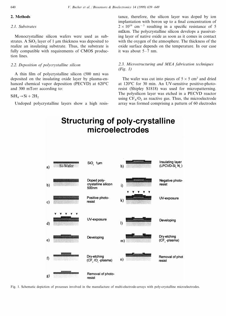
2.3. Microstructuring and MEA fabrication techniques(Fig. 1)
The wafer was cut into pieces of 5×5 cm2 and driedat 120°C for 30 min. An UV-sensitive positive-photo-resist (Shipley S1818) was used for micropatterning.The polysilicon layer was etched in a PECVD reactorusing CF4/O2 as reactive gas. Thus, the microelectrodearray was formed comprising a pattern of 60 electrodes
Fig. 1. Schematic depiction of processes involved in the manufacture of multi-electrode-arrays with poly-crystalline microelectrodes.
V. Bucher et al. / Biosensors & Bioelectronics 14 (1999) 639–649 641
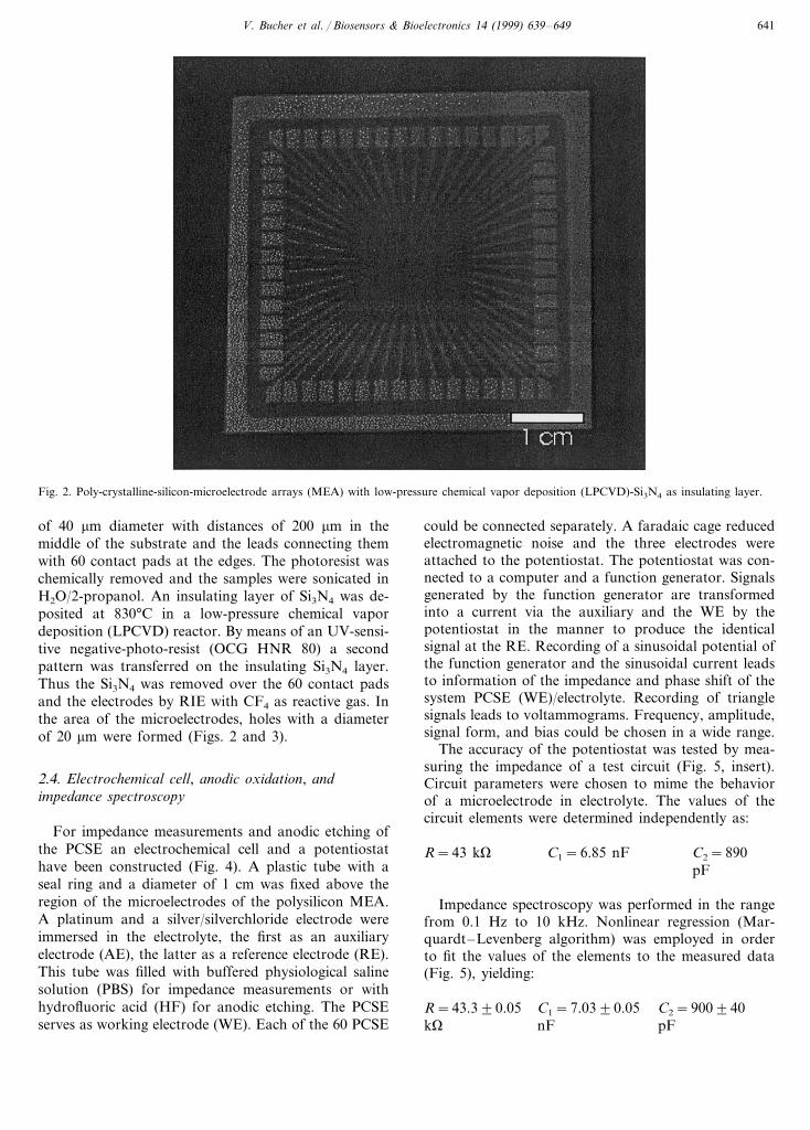
Fig. 2. Poly-crystalline-silicon-microelectrode arrays (MEA) with low-pressure chemical vapor deposition (LPCVD)-Si3N4 as insulating layer.
of 40 mm diameter with distances of 200 mm in themiddle of the substrate and the leads connecting themwith 60 contact pads at the edges. The photoresist waschemically removed and the samples were sonicated inH2O/2-propanol. An insulating layer of Si3N4 was de-posited at 830°C in a low-pressure chemical vapordeposition (LPCVD) reactor. By means of an UV-sensi-tive negative-photo-resist (OCG HNR 80) a secondpattern was transferred on the insulating Si3N4 layer.Thus the Si3N4 was removed over the 60 contact padsand the electrodes by RIE with CF4 as reactive gas. Inthe area of the microelectrodes, holes with a diameterof 20 mm were formed (Figs. 2 and 3).
2.4. Electrochemical cell, anodic oxidation, andimpedance spectroscopy
For impedance measurements and anodic etching ofthe PCSE an electrochemical cell and a potentiostathave been constructed (Fig. 4). A plastic tube with aseal ring and a diameter of 1 cm was fixed above theregion of the microelectrodes of the polysilicon MEA.A platinum and a silver/silverchloride electrode wereimmersed in the electrolyte, the first as an auxiliaryelectrode (AE), the latter as a reference electrode (RE).This tube was filled with buffered physiological salinesolution (PBS) for impedance measurements or withhydrofluoric acid (HF) for anodic etching. The PCSEserves as working electrode (WE). Each of the 60 PCSE
could be connected separately. A faradaic cage reducedelectromagnetic noise and the three electrodes wereattached to the potentiostat. The potentiostat was con-nected to a computer and a function generator. Signalsgenerated by the function generator are transformedinto a current via the auxiliary and the WE by thepotentiostat in the manner to produce the identicalsignal at the RE. Recording of a sinusoidal potential ofthe function generator and the sinusoidal current leadsto information of the impedance and phase shift of thesystem PCSE (WE)/electrolyte. Recording of trianglesignals leads to voltammograms. Frequency, amplitude,signal form, and bias could be chosen in a wide range.
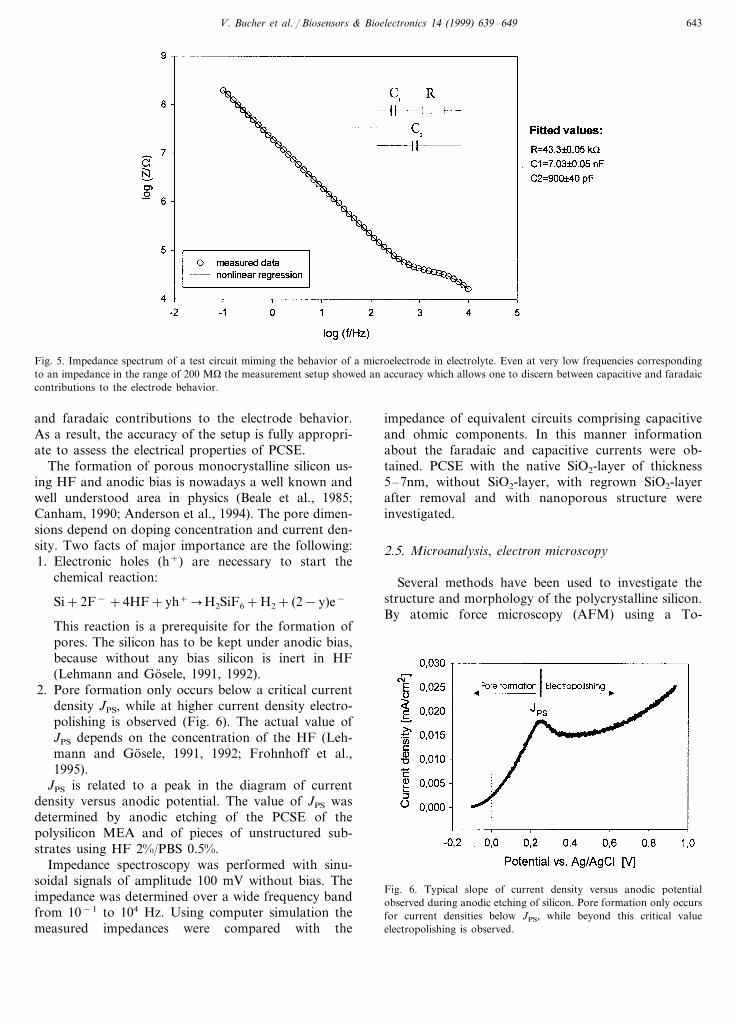
The accuracy of the potentiostat was tested by mea-suring the impedance of a test circuit (Fig. 5, insert).Circuit parameters were chosen to mime the behaviorof a microelectrode in electrolyte. The values of thecircuit elements were determined independently as:
C1=6.85 nF C2=890R=43 kVpF
Impedance spectroscopy was performed in the rangefrom 0.1 Hz to 10 kHz. Nonlinear regression (Mar-quardt–Levenberg algorithm) was employed in orderto fit the values of the elements to the measured data(Fig. 5), yielding:
R=43.390.05 C1=7.0390.05 C2=900940pFnFkV

V. Bucher et al. / Biosensors & Bioelectronics 14 (1999) 639–649642
The accuracy is B5% even at very low frequencieswhere circuit impedance exceeds 200 MV. This is par-
ticularly important, because only measurement at lowfrequencies allows one to discern between capacitive
Fig. 3. Thin-film microelectrode of a poly-crystalline-silicon-microelectrode arrays (MEA). Active area has a diameter of 20 mm.
Fig. 4. Schematic arrangement of the electrochemical cell for impedance measurements and anodic etching. Auxiliary electrode (AE): platinumwire. Reference electrode (RE): silver-silverchloride wire. Working electrode (WE): polysilicon microelectrode. The three electrodes were attachedto a potentiostat (A: ammeter, OA: operational amplifier, RP: reference potential).
V. Bucher et al. / Biosensors & Bioelectronics 14 (1999) 639–649 643
Fig. 5. Impedance spectrum of a test circuit miming the behavior of a microelectrode in electrolyte. Even at very low frequencies correspondingto an impedance in the range of 200 MV the measurement setup showed an accuracy which allows one to discern between capacitive and faradaiccontributions to the electrode behavior.
and faradaic contributions to the electrode behavior.As a result, the accuracy of the setup is fully appropri-ate to assess the electrical properties of PCSE.
The formation of porous monocrystalline silicon us-ing HF and anodic bias is nowadays a well known andwell understood area in physics (Beale et al., 1985;Canham, 1990; Anderson et al., 1994). The pore dimen-sions depend on doping concentration and current den-sity. Two facts of major importance are the following:1. Electronic holes (h+) are necessary to start the
chemical reaction:
Si+2F− +4HF+yh+�H2SiF6+H2+ (2−y)e−
This reaction is a prerequisite for the formation ofpores. The silicon has to be kept under anodic bias,because without any bias silicon is inert in HF(Lehmann and Gosele, 1991, 1992).
2. Pore formation only occurs below a critical currentdensity JPS, while at higher current density electro-polishing is observed (Fig. 6). The actual value ofJPS depends on the concentration of the HF (Leh-mann and Gosele, 1991, 1992; Frohnhoff et al.,1995).
JPS is related to a peak in the diagram of currentdensity versus anodic potential. The value of JPS wasdetermined by anodic etching of the PCSE of thepolysilicon MEA and of pieces of unstructured sub-strates using HF 2%/PBS 0.5%.
Impedance spectroscopy was performed with sinu-soidal signals of amplitude 100 mV without bias. Theimpedance was determined over a wide frequency bandfrom 10−1 to 104 Hz. Using computer simulation themeasured impedances were compared with the
impedance of equivalent circuits comprising capacitiveand ohmic components. In this manner informationabout the faradaic and capacitive currents were ob-tained. PCSE with the native SiO2-layer of thickness5–7nm, without SiO2-layer, with regrown SiO2-layerafter removal and with nanoporous structure wereinvestigated.
2.5. Microanalysis, electron microscopy
Several methods have been used to investigate thestructure and morphology of the polycrystalline silicon.By atomic force microscopy (AFM) using a To-
Fig. 6. Typical slope of current density versus anodic potentialobserved during anodic etching of silicon. Pore formation only occursfor current densities below JPS, while beyond this critical valueelectropolishing is observed.

V. Bucher et al. / Biosensors & Bioelectronics 14 (1999) 639–649644
Fig. 7. Atomic force microscopy (AFM) image of the poly-crystalline silicon surface (12×12 mm2). The linescan shows a considerable roughnessof the surface. Area RMS was determined to 6.35nm.
pometrix Explorer 2000 information about the surfacetexture was obtained, using scanning electron mi-croscopy (SEM) at 25 kV (Cambridge S-90) and trans-mission electron microscopy (TEM) at 200 kV (Jeol2000 FX-II) the crystalline structure, thickness of theSiO2 layer and the dimensions of the pores after anodicetching were revealed. For TEM examinations, thesamples were prepared using cross-sectional ionthinning.
3. Results and discussion
3.1. Morphology and nanostructure of polycrystallinethin films
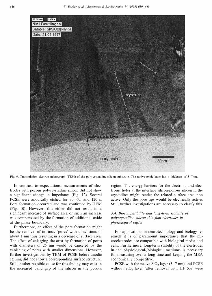
Scanning the surface of the polycrystalline silicon byAFM revealed a certain roughness (Fig. 7). The rough-ness of the surface of the PCSE was determined as 6.35nm RMS. Obviously the surface exhibits an intrinsicroughness in the as-deposited state which should affectthe impedance. Investigations of the cross-sections ofthe substrates by TEM revealed a size of the crystallitesranging from 50 to 500 nm (Fig. 8). This means that thebigger crystallites extend over the entire layer. Thenative oxide layer is about 5–7nm thick (Fig. 9). Nor-mally a thickness of 1–2nm would be expected. Thisfinding may easily be explained by the fact, that thewafer had a temperature of about 600°C when thereactor was opened after depositing polycrystalline sili-con. This increases the energy and thus the averagevelocity of the oxygen atoms. Indeed, a second nativeoxide layer grown at room temperature after removalof the first oxide layer by HF shows the expectedthickness of 1–2 nm.
3.2. Anodically etched polycrystalline silicon thin films
Using the potentiostat to record current-voltage-curves (CV-curves) the critical current density JPS wasdetermined. The PCSE was fixed in the electrochemicalcell. HF (2%) mixed with PBS (0.5%) to increase theconductivity served as etching medium. When com-pared to the values of JPS measured at bulk silicon(Zhang et al., 1989), polycrystalline silicon shows acritical current density which is about 1000 timessmaller. The JPS-peak in the CV-curve occurred at 18mA/cm2 (Fig. 6).
Consequently, PCSE were anodical etched at a biasU=0.2 V corresponding to a current density below JPS
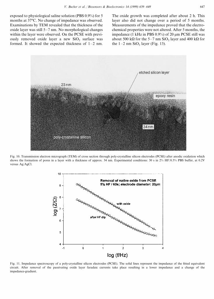
and the impedance of the electrodes was measuredsimultaneously at 1 kHz. An increasing surface areacaused by the pore formation should result in a lowerimpedance. However, no significant effect of the etchingprocess the impedance was found. Nevertheless, TEM-examinations confirmed the formation of pores with adiameter of up to 25 nm (Fig. 10). The growing velocitywas determined to 80 nm/min. These results will bediscussed more in detail below.
3.3. Impedance spectroscopy of the PCSE
Impedance spectroscopy in a frequency range from10−1 to 104 Hz of the PCSE at 100 mV amplitude wasperformed:1. On nonporous electrodes with thick SiO2 layer (5–7
nm), without an oxide layer and with thin SiO2 layer(1–2 nm).
2. On porous electrodes with different thickness of theporous surface.
V. Bucher et al. / Biosensors & Bioelectronics 14 (1999) 639–649 645
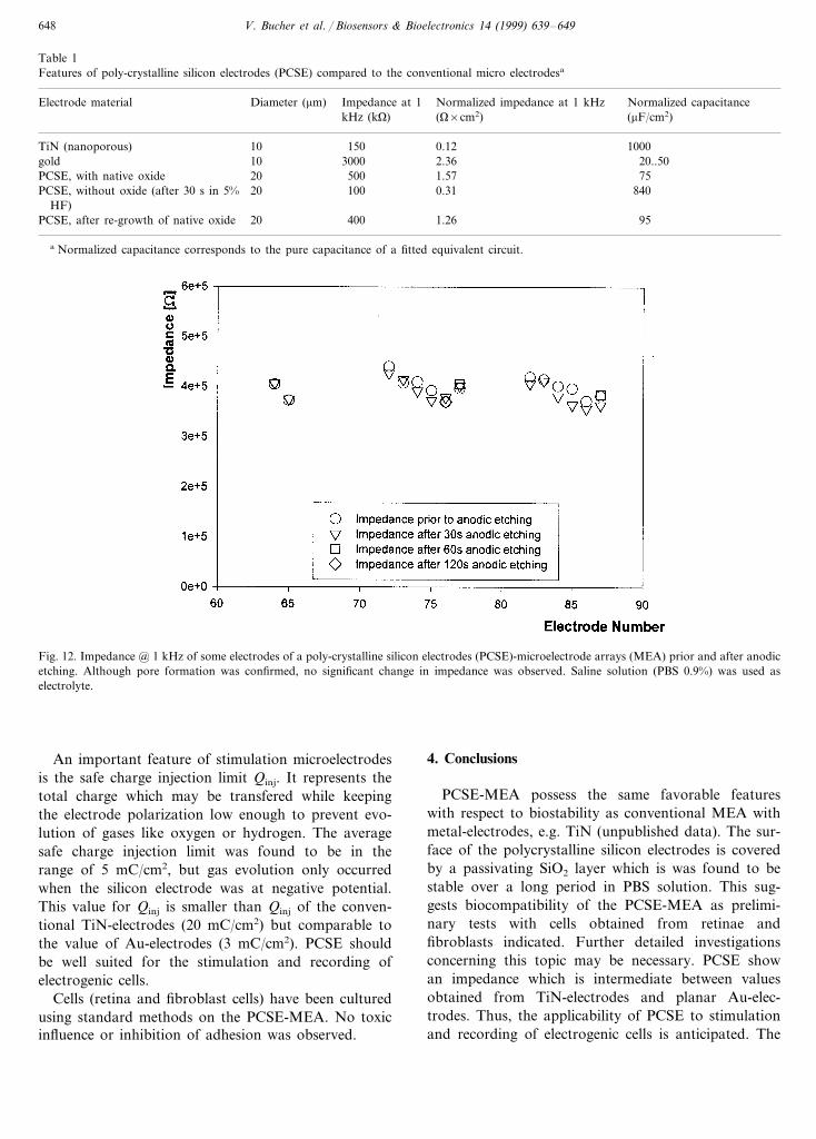
PCSE with an oxide layer show the behavior of aresistance and a capacitance in series without faradaiccontributions. The data obtained by impedance spec-troscopy were fitted to an equivalent circuit comprisinga pure resistance and capacitance in series. The shuntcapacity (an effect of the insulating layer above thelead) could be neglected. No faradaic current was ob-served, because the SiO2 layer inhibits electron transferand thus no redox reactions are observed.
PCSE without a SiO2 layer clearly show faradaiccontributions to the measured impedance. This may bededuced from the slope of the impedance curve (Fig.11). An equivalent circuit (Randles circuit) comprisinga resistance, R, as a series element followed by acapacitance, C, and faradaic impedance, ZF, as parallelelements representing the double-layer impedance wasfitted to the measured impedance data. The faradaicimpedance, ZF, is given by
ZF=s(1− i)
v
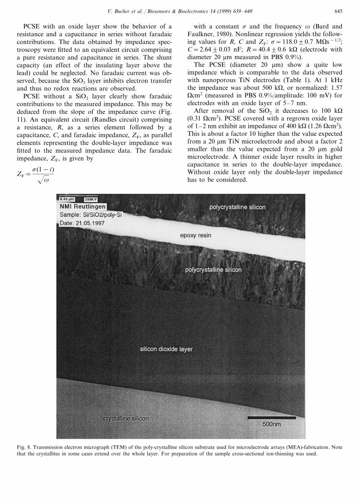
with a constant s and the frequency v (Bard andFaulkner, 1980). Nonlinear regression yields the follow-ing values for R, C and ZF: s=118.090.7 MVs−1/2;C=2.6490.03 nF; R=40.490.6 kV (electrode withdiameter 20 mm measured in PBS 0.9%).
The PCSE (diameter 20 mm) show a quite lowimpedance which is comparable to the data observedwith nanoporous TiN electrodes (Table 1). At 1 kHzthe impedance was about 500 kV, or normalized: 1.57Vcm2 (measured in PBS 0.9%/amplitude: 100 mV) forelectrodes with an oxide layer of 5–7 nm.
After removal of the SiO2 it decreases to 100 kV(0.31 Vcm2). PCSE covered with a regrown oxide layerof 1–2 nm exhibit an impedance of 400 kV (1.26 Vcm2).This is about a factor 10 higher than the value expectedfrom a 20 mm TiN microelectrode and about a factor 2smaller than the value expected from a 20 mm goldmicroelectrode. A thinner oxide layer results in highercapacitance in series to the double-layer impedance.Without oxide layer only the double-layer impedancehas to be considered.
Fig. 8. Transmission electron micrograph (TEM) of the poly-crystalline silicon substrate used for microelectrode arrays (MEA)-fabrication. Notethat the crystallites in some cases extend over the whole layer. For preparation of the sample cross-sectional ion-thinning was used.
V. Bucher et al. / Biosensors & Bioelectronics 14 (1999) 639–649646
Fig. 9. Transmission electron micrograph (TEM) of the poly-crystalline silicon substrate. The native oxide layer has a thickness of 5–7nm.
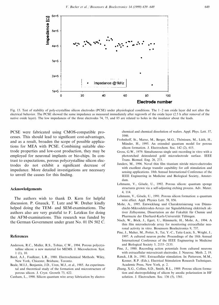
In contrast to expectations, measurements of elec-trodes with porous polycrystalline silicon did not showa significant change in impedance (Fig. 12). SeveralPCSE were anodically etched for 30, 60, and 120 s.Pore formation occurred and was confirmed by TEM(Fig. 10). However, this either did not result in asignificant increase of surface area or such an increasewas compensated by the formation of additional oxideat the phase boundary.
Furthermore, an effect of the pore formation mightbe the removal of intrinsic ‘pores’ with dimensions ofabout 1 nm thus resulting in a decrease of surface area.The effect of enlarging the area by formation of poreswith diameters of 25 nm would be canceled by thevanishing of pores with smaller dimensions. However,further investigations by TEM of PCSE before anodicetching did not show a corresponding surface structure.Still another possible cause for this finding may exist inthe increased band gap of the silicon in the porous
region. The energy barriers for the electrons and elec-tronic holes at the interface silicon/porous silicon in thecrystallites might render the related surface area nonactive. Only the pore tips would be electrically active.Still, further investigations are necessary to clarify this.
3.4. Biocompatibility and long-term stability ofpolycrystalline silicon thin-film electrodes inphysiological buffer
For applications in neurotechnology and biology re-search it is of paramount importance that the mi-croelectrodes are compatible with biological media andcells. Furthermore, long-term stability of the electrodesin the physiological-/biological mediums is necessaryfor measuring over a long time and keeping the MEAeconomically competitive.
PCSE with the native SiO2 layer (5–7 nm) and PCSEwithout SiO2 layer (after removal with HF 5%) were
V. Bucher et al. / Biosensors & Bioelectronics 14 (1999) 639–649 647
exposed to physiological saline solution (PBS 0.9%) for 5months at 37°C. No change of impedance was observed.Examinations by TEM revealed that the thickness of theoxide layer was still 5–7 nm. No morphological changeswithin the layer were observed. On the PCSE with previ-ously removed oxide layer a new SiO2 surface wasformed. It showed the expected thickness of 1–2 nm.
The oxide growth was completed after about 2 h. Thislayer also did not change over a period of 5 months.Measurements of the impedance proved that the electro-chemical properties were not altered. After 5 months, theimpedance (1 kHz in PBS 0.9%) of 20 mm PCSE still wasabout 500 kV for the 5–7 nm SiO2 layer and 400 kV forthe 1–2 nm SiO2 layer (Fig. 13).
Fig. 10. Transmission electron micrograph (TEM) of cross section through poly-crystalline silicon electrodes (PCSE) after anodic oxidation whichshows the formation of pores in a layer with a thickness of approx. 34 nm. Experimental conditions: 30 s in 2% HF/0.5% PBS buffer, at 0.2Vversus Ag/AgCl.
Fig. 11. Impedance spectroscopy of a poly-crystalline silicon electrodes (PCSE). The solid lines represent the impedance of the fitted equivalentcircuit. After removal of the passivating oxide layer faradaic currents take place resulting in a lower impedance and a change of theimpedance-gradient.
V. Bucher et al. / Biosensors & Bioelectronics 14 (1999) 639–649648
Table 1Features of poly-crystalline silicon electrodes (PCSE) compared to the conventional micro electrodesa
Electrode material Diameter (mm) Impedance at 1 Normalized impedance at 1 kHz Normalized capacitance(mF/cm2)(V×cm2)kHz (kV)
TiN (nanoporous) 15010 0.12 10003000 2.3610 20..50gold
500 1.57PCSE, with native oxide 752020 100 0.31PCSE, without oxide (after 30 s in 5% 840
HF)PCSE, after re-growth of native oxide 40020 1.26 95
a Normalized capacitance corresponds to the pure capacitance of a fitted equivalent circuit.
Fig. 12. Impedance @ 1 kHz of some electrodes of a poly-crystalline silicon electrodes (PCSE)-microelectrode arrays (MEA) prior and after anodicetching. Although pore formation was confirmed, no significant change in impedance was observed. Saline solution (PBS 0.9%) was used aselectrolyte.
An important feature of stimulation microelectrodesis the safe charge injection limit Qinj. It represents thetotal charge which may be transfered while keepingthe electrode polarization low enough to prevent evo-lution of gases like oxygen or hydrogen. The averagesafe charge injection limit was found to be in therange of 5 mC/cm2, but gas evolution only occurredwhen the silicon electrode was at negative potential.This value for Qinj is smaller than Qinj of the conven-tional TiN-electrodes (20 mC/cm2) but comparable tothe value of Au-electrodes (3 mC/cm2). PCSE shouldbe well suited for the stimulation and recording ofelectrogenic cells.
Cells (retina and fibroblast cells) have been culturedusing standard methods on the PCSE-MEA. No toxicinfluence or inhibition of adhesion was observed.
4. Conclusions
PCSE-MEA possess the same favorable featureswith respect to biostability as conventional MEA withmetal-electrodes, e.g. TiN (unpublished data). The sur-face of the polycrystalline silicon electrodes is coveredby a passivating SiO2 layer which is was found to bestable over a long period in PBS solution. This sug-gests biocompatibility of the PCSE-MEA as prelimi-nary tests with cells obtained from retinae andfibroblasts indicated. Further detailed investigationsconcerning this topic may be necessary. PCSE showan impedance which is intermediate between valuesobtained from TiN-electrodes and planar Au-elec-trodes. Thus, the applicability of PCSE to stimulationand recording of electrogenic cells is anticipated. The
V. Bucher et al. / Biosensors & Bioelectronics 14 (1999) 639–649 649
Fig. 13. Test of stability of poly-crystalline silicon electrodes (PCSE) under physiological conditions. The 1–2 nm oxide layer did not alter theelectrical behavior. The PCSE showed the same impedance as measured immediately after regrowth of the oxide layer (2.5 h after removal of thenative oxide layer). The low impedances of the three electrodes 74, 75, and 85 are related to holes in the insulator about the leads.
PCSE were fabricated using CMOS-compatible pro-cesses. This should lead to significant cost-advantages,and as a result, broaden the scope of possible applica-tions for MEA with PCSE. Combining suitable elec-trode properties and low-cost production, they may beemployed for neuronal implants or bio-chips. In con-trast to expectations, porous polycrystalline silicon elec-trodes do not exhibit a significant decrease ofimpedance. More detailed investigations are necessaryto unveil the causes for this finding.
Acknowledgements
The authors wish to thank D. Kern for helpfuldiscussion. P. Gnauck, T. Lutz and W. Dreher kindlyhelped doing the TEM- and SEM-examinations. Theauthors also are very grateful to F. Letzkus for doingthe AFM-examinations. This research was funded bythe German Government under grant No. 01 IN 502 C.
References
Anderson, R.C., Muller, R.S., Tobias, C.W., 1994. Porous polycrys-talline silicon: a new material for MEMS. J. Microelectron. Syst.1 (1), 10.
Bard, A.J., Faulkner, L.R., 1980. Electrochemical Methods. Wiley,New York, Chicester, Brisbane, Toronto.
Beale, M.I.J., Benjamin, J.D., Uren, M.J., et al., 1985. An experimen-tal and theoretical study of the formation and microstructure ofporous silicon. J. Cryst. Growth 73, 622.
Canham, L., 1990. Silicon quantum wire array fabrication by electro-
chemical and chemical dissolution of wafers. Appl. Phys. Lett. 57,1046.
Frohnhoff, St., Marso, M., Berger, M.G., Thonissen, M., Luth, H.,Munder, H., 1995. An extended quantum model for poroussilicon formation. J. Electrochem. Soc. 142 (2), 615.
Gross, G.W., 1979. Simultaneous single unit recording in vitro with aphotoetched deinsulated gold microelectrode surface. IEEETrans. Biomed. Eng. 26, 273.
Janders, M., 1996. Novel thin film titanium nitride micro-electrodeswith excellent charge transfer capability for cell stimulation andsensing applications. 18th Annual International Conference of theIEEE Engineering in Medicine and Biological Society, Amster-dam.
Lehmann, V., Gosele, U., 1992. Porous silicon: quantum spongestructures grown via a self-adjusting etching process. Adv. Mater.4, 114.
Lehmann, V., Gosele, U., 1991. Porous silicon formation: a quantumwire effect. Appl. Physics Lett. 58, 856.
Mohr, A., 1995. Entwicklung und Charakterisierung von Dunns-chicht-Mikroelektroden-Arrays zur Signalableitung elektrisch ak-tiver Zellsysteme, Dissertation an der Fakultat fur Chemie undPharmazie der Eberhard-Karls-Universitat Tubingen.
Nisch, W., Bock, J., Egert, U., Hammerle, H., Mohr, A., 1994. Athin film microelectrode array for monitoring extracellular neu-ronal activity in vitro. Biosensors Bioelectronics 9, 737.
Pine, J., Maher, M., Potter, S., Tai, Y.-C., Tatic-Lucic, S., Wright, J.,1997. A cultured neuron probe: Proceedings of the 18th AnnualInternational Conference of the IEEE Engineering in Medicineand Biological Society 5, 2133–2135.
Pine, J., 1980. Recording action potentials from cultured neuronswith extracellular microcircuit electrodes. J. Neurosc. Meth. 2, 19.
Ranck, J.B. Jr., 1981. Extracellular stimulation. In: Patterson, M.M.,Kesner, R.P. (Eds.), Electrical Stimulation Research Techniques.Academic Press, New York, p. 2.
Zhang, X.G., Collins, S.D., Smith, R.L., 1989. Porous silicon forma-tion and electropolishing of silicon by anodic polarization in HFsolution. J. Electrochem. Soc. 136 (5), 1561.
.