Low-bias negative differential resistance in graphene nanoribbon superlattices
6
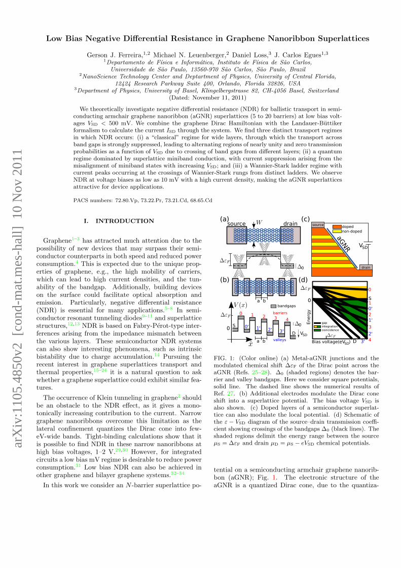
Low Bias Negative Differential Resistance in Graphene Nanoribbon Superlattices Gerson J. Ferreira, 1,2 Michael N. Leuenberger, 2 Daniel Loss, 3 J. Carlos Egues 1,3 1 Departamento de F´ ısica e Inform´ atica, Instituto de F´ ısica de S˜ ao Carlos, Universidade de S˜ ao Paulo, 13560-970 S˜ao Carlos, S˜ao Paulo, Brazil 2 NanoScience Technology Center and Deptartment of Physics, University of Central Florida, 12424 Research Parkway Suite 400, Orlando, Florida 32826, USA 3 Department of Physics, University of Basel, Klingelbergstrasse 82, CH-4056 Basel, Switzerland (Dated: November 11, 2011) We theoretically investigate negative differential resistance (NDR) for ballistic transport in semi- conducting armchair graphene nanoribbon (aGNR) superlattices (5 to 20 barriers) at low bias volt- ages VSD < 500 mV. We combine the graphene Dirac Hamiltonian with the Landauer-B¨ uttiker formalism to calculate the current ISD through the system. We find three distinct transport regimes in which NDR occurs: (i) a “classical” regime for wide layers, through which the transport across band gaps is strongly suppressed, leading to alternating regions of nearly unity and zero transmission probabilities as a function of VSD due to crossing of band gaps from different layers; (ii) a quantum regime dominated by superlattice miniband conduction, with current suppression arising from the misalignment of miniband states with increasing VSD; and (iii) a Wannier-Stark ladder regime with current peaks occurring at the crossings of Wannier-Stark rungs from distinct ladders. We observe NDR at voltage biases as low as 10 mV with a high current density, making the aGNR superlattices attractive for device applications. PACS numbers: 72.80.Vp, 73.22.Pr, 73.21.Cd, 68.65.Cd I. INTRODUCTION Graphene 1–3 has attracted much attention due to the possibility of new devices that may surpass their semi- conductor counterparts in both speed and reduced power consumption. 4 This is expected due to the unique prop- erties of graphene, e.g., the high mobility of carriers, which can lead to high current densities, and the tun- ability of the bandgap. Additionally, building devices on the surface could facilitate optical absorption and emission. Particularly, negative differential resistance (NDR) is essential for many applications. 5–8 In semi- conductor resonant tunneling diodes 9–11 and superlattice structures, 12,13 NDR is based on Fabry-P´ erot-type inter- ferences arising from the impedance mismatch between the various layers. These semiconductor NDR systems can also show interesting phenomena, such as intrinsic bistability due to charge accumulation. 14 Pursuing the recent interest in graphene superlattices transport and thermal properties, 15–24 it is a natural question to ask whether a graphene superlattice could exhibit similar fea- tures. The occurrence of Klein tunneling in graphene 2 should be an obstacle to the NDR effect, as it gives a mono- tonically increasing contribution to the current. Narrow graphene nanoribbons overcome this limitation as the lateral confinement quantizes the Dirac cone into few- eV-wide bands. Tight-binding calculations show that it is possible to find NDR in these narrow nanoribbons at high bias voltages, 1–2 V. 29,30 However, for integrated circuits a low bias mV regime is desirable to reduce power consumption. 31 Low bias NDR can also be achieved in other graphene and bilayer graphene systems. 32–34 In this work we consider an N -barrier superlattice po- 0 1 2 3 4 0' 1' 2' 3' S Bias voltage( ) Energy gap integration coincidence 0 (a) (c) (d) 0 0' S 0 aGNR (b) a b source drain source drain doped non-doped V SD eV SD D 1' 2' 3' 1 2 3 4 V SD a b bandgaps valleys barriers 0 D 0 FIG. 1: (Color online) (a) Metal-aGNR junctions and the modulated chemical shift ΔεF of the Dirac point across the aGNR (Refs. 25–28). Δ0 (shaded regions) denotes the bar- rier and valley bandgaps. Here we consider square potentials, solid line. The dashed line shows the numerical results of Ref. 27. (b) Additional electrodes modulate the Dirac cone shift into a superlattice potential. The bias voltage VSD is also shown. (c) Doped layers of a semiconductor superlat- tice can also modulate the local potential. (d) Schematic of the ε - VSD diagram of the source–drain transmission coeffi- cient showing crossings of the bandgaps Δ0 (black lines). The shaded regions delimit the energy range between the source μS =ΔεF and drain μD = μS - eVSD chemical potentials. tential on a semiconducting armchair graphene nanorib- bon (aGNR); Fig. 1. The electronic structure of the aGNR is a quantized Dirac cone, due to the quantiza- arXiv:1105.4850v2 [cond-mat.mes-hall] 10 Nov 2011
-
Upload
independent -
Category
Documents
-
view
0 -
download
0
Transcript of Low-bias negative differential resistance in graphene nanoribbon superlattices
Low Bias Negative Differential Resistance in Graphene Nanoribbon Superlattices
Gerson J. Ferreira,1,2 Michael N. Leuenberger,2 Daniel Loss,3 J. Carlos Egues1,31Departamento de Fısica e Informatica, Instituto de Fısica de Sao Carlos,
Universidade de Sao Paulo, 13560-970 Sao Carlos, Sao Paulo, Brazil2NanoScience Technology Center and Deptartment of Physics, University of Central Florida,
12424 Research Parkway Suite 400, Orlando, Florida 32826, USA3Department of Physics, University of Basel, Klingelbergstrasse 82, CH-4056 Basel, Switzerland
(Dated: November 11, 2011)
We theoretically investigate negative differential resistance (NDR) for ballistic transport in semi-conducting armchair graphene nanoribbon (aGNR) superlattices (5 to 20 barriers) at low bias volt-ages VSD < 500 mV. We combine the graphene Dirac Hamiltonian with the Landauer-Buttikerformalism to calculate the current ISD through the system. We find three distinct transport regimesin which NDR occurs: (i) a “classical” regime for wide layers, through which the transport acrossband gaps is strongly suppressed, leading to alternating regions of nearly unity and zero transmissionprobabilities as a function of VSD due to crossing of band gaps from different layers; (ii) a quantumregime dominated by superlattice miniband conduction, with current suppression arising from themisalignment of miniband states with increasing VSD; and (iii) a Wannier-Stark ladder regime withcurrent peaks occurring at the crossings of Wannier-Stark rungs from distinct ladders. We observeNDR at voltage biases as low as 10 mV with a high current density, making the aGNR superlatticesattractive for device applications.
PACS numbers: 72.80.Vp, 73.22.Pr, 73.21.Cd, 68.65.Cd
I. INTRODUCTION
Graphene1–3 has attracted much attention due to thepossibility of new devices that may surpass their semi-conductor counterparts in both speed and reduced powerconsumption.4 This is expected due to the unique prop-erties of graphene, e.g., the high mobility of carriers,which can lead to high current densities, and the tun-ability of the bandgap. Additionally, building deviceson the surface could facilitate optical absorption andemission. Particularly, negative differential resistance(NDR) is essential for many applications.5–8 In semi-conductor resonant tunneling diodes9–11 and superlatticestructures,12,13 NDR is based on Fabry-Perot-type inter-ferences arising from the impedance mismatch betweenthe various layers. These semiconductor NDR systemscan also show interesting phenomena, such as intrinsicbistability due to charge accumulation.14 Pursuing therecent interest in graphene superlattices transport andthermal properties,15–24 it is a natural question to askwhether a graphene superlattice could exhibit similar fea-tures.
The occurrence of Klein tunneling in graphene2 shouldbe an obstacle to the NDR effect, as it gives a mono-tonically increasing contribution to the current. Narrowgraphene nanoribbons overcome this limitation as thelateral confinement quantizes the Dirac cone into few-eV-wide bands. Tight-binding calculations show that itis possible to find NDR in these narrow nanoribbons athigh bias voltages, 1–2 V.29,30 However, for integratedcircuits a low bias mV regime is desirable to reduce powerconsumption.31 Low bias NDR can also be achieved inother graphene and bilayer graphene systems.32–34
In this work we consider an N -barrier superlattice po-
0
1
2
3
4
0'
1'
2'
3'
S
Bias voltage( )
Energ
y
gapintegrationcoincidence
0
(a) (c)
(d)
0
0'S0
aGNR
(b)
a b
source drain source
drain
dopednon-doped
VSD
eVSD
D1' 2' 3'
1 2 3 4
VSD
a b
bandgaps
valleys
barriers
0
D
0
FIG. 1: (Color online) (a) Metal-aGNR junctions and themodulated chemical shift ∆εF of the Dirac point across theaGNR (Refs. 25–28). ∆0 (shaded regions) denotes the bar-rier and valley bandgaps. Here we consider square potentials,solid line. The dashed line shows the numerical results ofRef. 27. (b) Additional electrodes modulate the Dirac coneshift into a superlattice potential. The bias voltage VSD isalso shown. (c) Doped layers of a semiconductor superlat-tice can also modulate the local potential. (d) Schematic ofthe ε − VSD diagram of the source–drain transmission coeffi-cient showing crossings of the bandgaps ∆0 (black lines). Theshaded regions delimit the energy range between the sourceµS = ∆εF and drain µD = µS − eVSD chemical potentials.
tential on a semiconducting armchair graphene nanorib-bon (aGNR); Fig. 1. The electronic structure of theaGNR is a quantized Dirac cone, due to the quantiza-
arX
iv:1
105.
4850
v2 [
cond
-mat
.mes
-hal
l] 1
0 N
ov 2
011
2
tion of the transversal momentum kn, and can be metal-lic, kn0 = 0, or semiconducting, kn0 6= 0, dependingon the width W of the nanoribbon; kn0 is the closestto zero transverse momenta. We choose W = 346a0,such that the aGNR is semiconducting with a bandgap∆0 = 28 meV; a0 = 0.142 nm is the C-C distance. Weuse the transfer-matrix formalism to calculate the source-drain transmission coefficient TSD across the superlatticepotential along the aGNR, considering a finite bias volt-age VSD, revealing the electronic structure of the system;Fig. 2. The potential drop from source to drain follows apiecewise constant profile layer by layer; Fig. 1(b). Thecurrent is calculated within the usual Landauer-Buttikerformalism.
We find low bias NDR at zero and room temperatureswithin three distinct physical regimes. (i) For wide lay-ers, the transmission across the bandgaps ∆0 is stronglysuppressed, and nearly unity for energies away from thebandgaps. With increasing voltage, both barrier andvalley bandgaps split and cross as shown schematicallyin Fig. 1(d), showing, at the coincidence region, a pat-tern of diamond-shaped structures with alternating re-gions of finite and suppressed transmission, thus leadingto NDR. For narrow barriers resonant tunneling acrosslayers become relevant. (ii) At zero bias, hybridizationof resonant modes leads to minibands with finite, nearlyunity, transmission; Fig. 2(b)-2(e). At very low voltageseVSD ∼ 10 meV (of the order of the miniband energywidth) the resonant states misalign, thus breaking theminibands into off-resonance Wannier-Stark ladders withsuppressed transmission. This gives rise to a single cur-rent spike near eVSD ∼ 10 meV. (iii) With increasingeVSD, rungs of ladders from distinct minibands cross andhybridize, showing a new set of resonant spikes in TSD,Fig. 2(a), thus leading to current spikes and NDR.
II. PROPOSED SYSTEM & MODEL
The modulation of the Dirac cone into a superlatticepotential can be achieved by different setups. It wasshown that local charge-transfer effects between grapheneand some metals (e.g., Al, Cu, Ag, Au, Pt) rigidly shiftsthe Dirac cone;25–28 Fig. 1(a). A series of metallic stripesover graphene can create the proposed superlattice po-tential; Fig. 1(b). Equivalently, the same structure canbe obtained by selectively doping graphene regions in analternate fashion. Additionally, the aGNR could be ar-ranged along the doped/non-doped layers of a cleavedsemiconductor heterostructure;35 Fig. 1(c). Narrow sys-tems (. 400 nm) are desirable to keep transport ballisticat room temperatures.
We consider low-energy excitations of graphenewithin the envelope function approximation,3,36 i.e., thegraphene Dirac Hamiltonian. The finite size of thenanoribbon requires vanishing wave functions at theedges, where for aGNR both A and B sublattices ofthe honeycomb lattice are present. This leads to van-
(c) 2 barriers
D0
0 0.5 1
B*
Transmission TSD
(d) 5 barriers
0 0.5 1
A
B
C
Energy (m
eV)
(e) 20 barriers
0 0.5 1160
180
200
220
240
260
280
300(a)
0 25 50 75 100
Bias Voltage (mV)
190
210
230
250
270
Ene
rgy
(meV
)
0
1
TSD
A
B
C
(b)
D0
b a b
B*
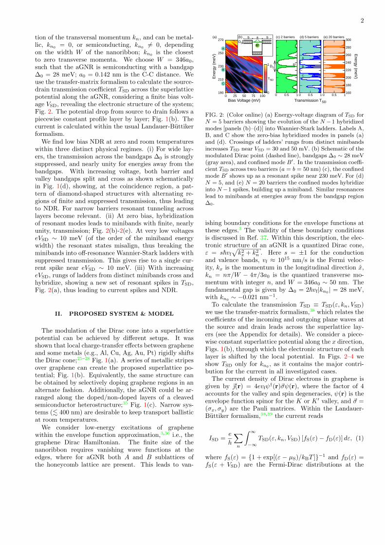
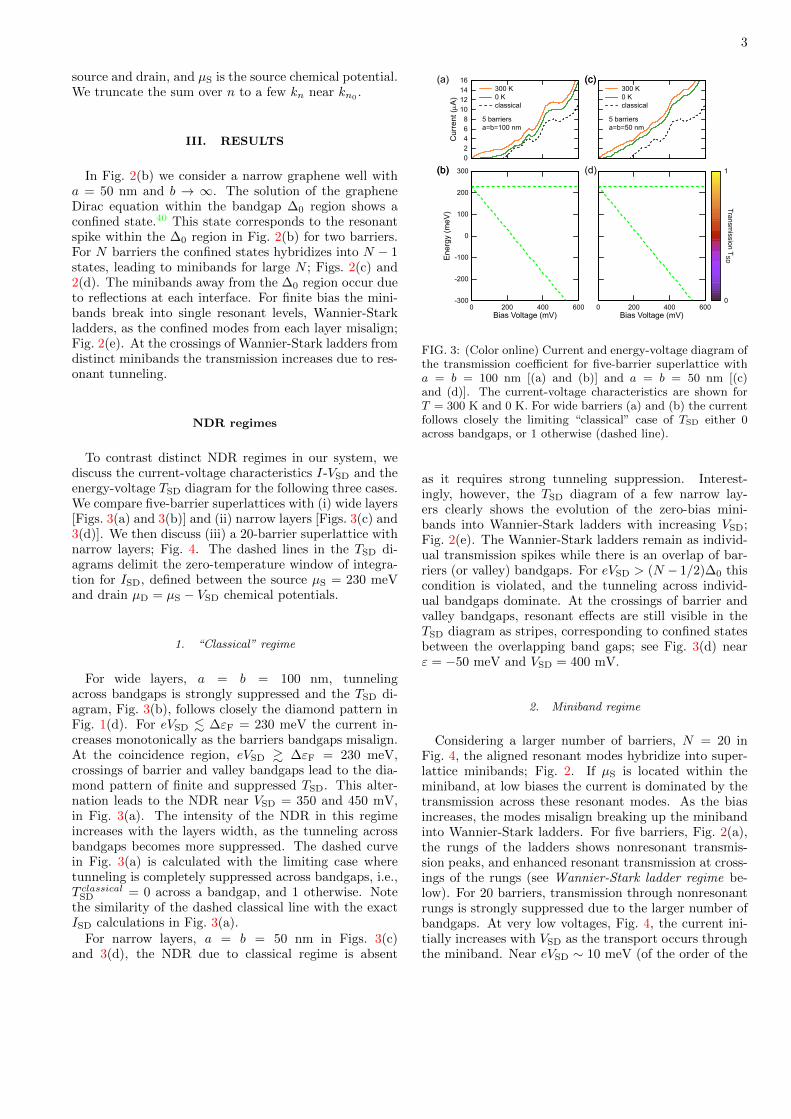
FIG. 2: (Color online) (a) Energy-voltage diagram of TSD forN = 5 barriers showing the evolution of the N − 1 hybridizedmodes [panels (b)–(d)] into Wannier-Stark ladders. Labels A,B, and C show the zero-bias hybridized modes in panels (a)and (d). Crossings of ladders’ rungs from distinct minibandsincreases TSD near VSD = 30 and 50 mV. (b) Schematic of themodulated Dirac point (dashed line), bandgaps ∆0 ∼ 28 meV(gray area), and confined mode B′. In the transmission coeffi-cient TSD across two barriers (a = b = 50 nm) (c), the confinedmode B′ shows up as a resonant spike near 230 meV. For (d)N = 5, and (e) N = 20 barriers the confined modes hybridizeinto N−1 spikes, building up a miniband. Similar resonanceslead to minibands at energies away from the bandgap region∆0.
ishing boundary conditions for the envelope functions atthese edges.3 The validity of these boundary conditionsis discussed in Ref. 37. Within this description, the elec-tronic structure of an aGNR is a quantized Dirac cone,ε = s~vf
√k2x + k2n . Here s = ±1 for the conduction
and valence bands, vf ≈ 1015 nm/s is the Fermi veloc-ity, kx is the momentum in the longitudinal direction x,kn = nπ/W − 4π/3a0 is the quantized transverse mo-mentum with integer n, and W = 346a0 ∼ 50 nm. Thefundamental gap is given by ∆0 = 2~vf|kn0
| = 28 meV,with kn0 ∼ −0.021 nm−1.
To calculate the transmission TSD ≡ TSD(ε, kn, VSD)we use the transfer-matrix formalism,38 which relates thecoefficients of the incoming and outgoing plane waves atthe source and drain leads across the superlattice lay-ers (see the Appendix for details). We consider a piece-wise constant superlattice potential along the x direction,Figs. 1(b), through which the electronic structure of eachlayer is shifted by the local potential. In Figs. 2–4 weshow TSD only for kn0
, as it contains the major contri-bution for the current in all investigated cases.
The current density of Dirac electrons in graphene isgiven by ~(r) = 4evfψ
†(r)~σψ(r), where the factor of 4accounts for the valley and spin degeneracies, ψ(r) is theenvelope function spinor for the K or K ′ valley, and ~σ =(σx, σy) are the Pauli matrices. Within the Landauer-Buttiker formalism,38,39 the current reads
ISD =e
h
∑n
∫ ∞−∞
TSD(ε, kn, VSD) [fS(ε)− fD(ε)] dε, (1)
where fS(ε) = {1 + exp[(ε − µS)/kBT ]}−1 and fD(ε) =fS(ε + VSD) are the Fermi-Dirac distributions at the
3
source and drain, and µS is the source chemical potential.We truncate the sum over n to a few kn near kn0 .
III. RESULTS
In Fig. 2(b) we consider a narrow graphene well witha = 50 nm and b → ∞. The solution of the grapheneDirac equation within the bandgap ∆0 region shows aconfined state.40 This state corresponds to the resonantspike within the ∆0 region in Fig. 2(b) for two barriers.For N barriers the confined states hybridizes into N − 1states, leading to minibands for large N ; Figs. 2(c) and2(d). The minibands away from the ∆0 region occur dueto reflections at each interface. For finite bias the mini-bands break into single resonant levels, Wannier-Starkladders, as the confined modes from each layer misalign;Fig. 2(e). At the crossings of Wannier-Stark ladders fromdistinct minibands the transmission increases due to res-onant tunneling.
NDR regimes
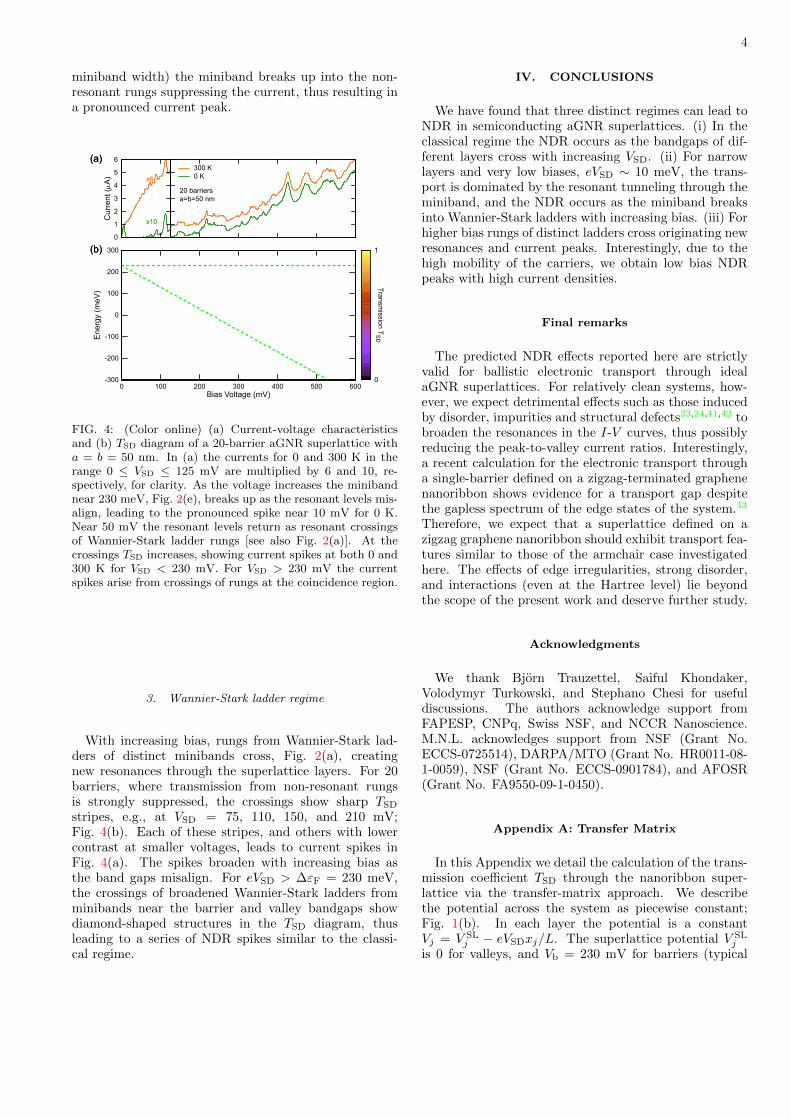
To contrast distinct NDR regimes in our system, wediscuss the current-voltage characteristics I-VSD and theenergy-voltage TSD diagram for the following three cases.We compare five-barrier superlattices with (i) wide layers[Figs. 3(a) and 3(b)] and (ii) narrow layers [Figs. 3(c) and3(d)]. We then discuss (iii) a 20-barrier superlattice withnarrow layers; Fig. 4. The dashed lines in the TSD di-agrams delimit the zero-temperature window of integra-tion for ISD, defined between the source µS = 230 meVand drain µD = µS − VSD chemical potentials.
1. “Classical” regime
For wide layers, a = b = 100 nm, tunnelingacross bandgaps is strongly suppressed and the TSD di-agram, Fig. 3(b), follows closely the diamond pattern inFig. 1(d). For eVSD . ∆εF = 230 meV the current in-creases monotonically as the barriers bandgaps misalign.At the coincidence region, eVSD & ∆εF = 230 meV,crossings of barrier and valley bandgaps lead to the dia-mond pattern of finite and suppressed TSD. This alter-nation leads to the NDR near VSD = 350 and 450 mV,in Fig. 3(a). The intensity of the NDR in this regimeincreases with the layers width, as the tunneling acrossbandgaps becomes more suppressed. The dashed curvein Fig. 3(a) is calculated with the limiting case wheretunneling is completely suppressed across bandgaps, i.e.,T classicalSD = 0 across a bandgap, and 1 otherwise. Notethe similarity of the dashed classical line with the exactISD calculations in Fig. 3(a).
For narrow layers, a = b = 50 nm in Figs. 3(c)and 3(d), the NDR due to classical regime is absent
(b)
0 200 400 600Bias Voltage (mV)
-300
-200
-100
0
100
200
300
Ene
rgy
(meV
)
(b)
Cur
rent
(�A
)
(a)
5 barriersa=b=100 nm
300 K0 Kclassical
0
2
46
8
10
1214
16 (c)
0 200 400 600Bias Voltage (mV)
0
1
Transm
ission TS
D
(c)
(d)
5 barriersa=b=50 nm
300 K0 Kclassical
FIG. 3: (Color online) Current and energy-voltage diagram ofthe transmission coefficient for five-barrier superlattice witha = b = 100 nm [(a) and (b)] and a = b = 50 nm [(c)and (d)]. The current-voltage characteristics are shown forT = 300 K and 0 K. For wide barriers (a) and (b) the currentfollows closely the limiting “classical” case of TSD either 0across bandgaps, or 1 otherwise (dashed line).
as it requires strong tunneling suppression. Interest-ingly, however, the TSD diagram of a few narrow lay-ers clearly shows the evolution of the zero-bias mini-bands into Wannier-Stark ladders with increasing VSD;Fig. 2(e). The Wannier-Stark ladders remain as individ-ual transmission spikes while there is an overlap of bar-riers (or valley) bandgaps. For eVSD > (N − 1/2)∆0 thiscondition is violated, and the tunneling across individ-ual bandgaps dominate. At the crossings of barrier andvalley bandgaps, resonant effects are still visible in theTSD diagram as stripes, corresponding to confined statesbetween the overlapping band gaps; see Fig. 3(d) nearε = −50 meV and VSD = 400 mV.
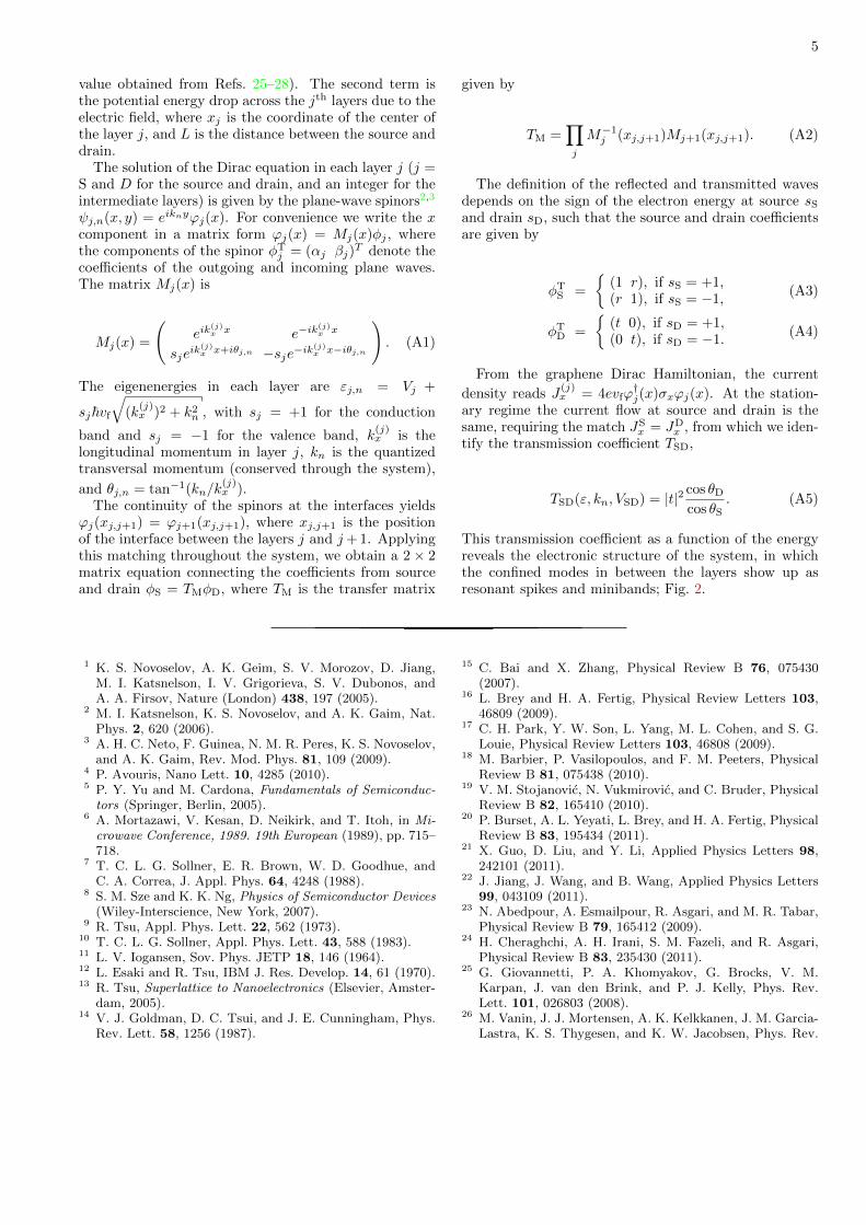
2. Miniband regime
Considering a larger number of barriers, N = 20 inFig. 4, the aligned resonant modes hybridize into super-lattice minibands; Fig. 2. If µS is located within theminiband, at low biases the current is dominated by thetransmission across these resonant modes. As the biasincreases, the modes misalign breaking up the minibandinto Wannier-Stark ladders. For five barriers, Fig. 2(a),the rungs of the ladders shows nonresonant transmis-sion peaks, and enhanced resonant transmission at cross-ings of the rungs (see Wannier-Stark ladder regime be-low). For 20 barriers, transmission through nonresonantrungs is strongly suppressed due to the larger number ofbandgaps. At very low voltages, Fig. 4, the current ini-tially increases with VSD as the transport occurs throughthe miniband. Near eVSD ∼ 10 meV (of the order of the
4
miniband width) the miniband breaks up into the non-resonant rungs suppressing the current, thus resulting ina pronounced current peak.
(b)
0 100 200 300 400 500 600Bias Voltage (mV)
-300
-200
-100
0
100
200
300
Ene
rgy
(meV
)
0
1
Transm
ission TS
D
(b)
Cur
rent
(�A
)
(a)
0
1
2
3
4
5
6
x6
x10
(a)
20 barriersa=b=50 nm
300 K0 K
FIG. 4: (Color online) (a) Current-voltage characteristicsand (b) TSD diagram of a 20-barrier aGNR superlattice witha = b = 50 nm. In (a) the currents for 0 and 300 K in therange 0 ≤ VSD ≤ 125 mV are multiplied by 6 and 10, re-spectively, for clarity. As the voltage increases the minibandnear 230 meV, Fig. 2(e), breaks up as the resonant levels mis-align, leading to the pronounced spike near 10 mV for 0 K.Near 50 mV the resonant levels return as resonant crossingsof Wannier-Stark ladder rungs [see also Fig. 2(a)]. At thecrossings TSD increases, showing current spikes at both 0 and300 K for VSD < 230 mV. For VSD > 230 mV the currentspikes arise from crossings of rungs at the coincidence region.
3. Wannier-Stark ladder regime
With increasing bias, rungs from Wannier-Stark lad-ders of distinct minibands cross, Fig. 2(a), creatingnew resonances through the superlattice layers. For 20barriers, where transmission from non-resonant rungsis strongly suppressed, the crossings show sharp TSDstripes, e.g., at VSD = 75, 110, 150, and 210 mV;Fig. 4(b). Each of these stripes, and others with lowercontrast at smaller voltages, leads to current spikes inFig. 4(a). The spikes broaden with increasing bias asthe band gaps misalign. For eVSD > ∆εF = 230 meV,the crossings of broadened Wannier-Stark ladders fromminibands near the barrier and valley bandgaps showdiamond-shaped structures in the TSD diagram, thusleading to a series of NDR spikes similar to the classi-cal regime.
IV. CONCLUSIONS
We have found that three distinct regimes can lead toNDR in semiconducting aGNR superlattices. (i) In theclassical regime the NDR occurs as the bandgaps of dif-ferent layers cross with increasing VSD. (ii) For narrowlayers and very low biases, eVSD ∼ 10 meV, the trans-port is dominated by the resonant tunneling through theminiband, and the NDR occurs as the miniband breaksinto Wannier-Stark ladders with increasing bias. (iii) Forhigher bias rungs of distinct ladders cross originating newresonances and current peaks. Interestingly, due to thehigh mobility of the carriers, we obtain low bias NDRpeaks with high current densities.
Final remarks
The predicted NDR effects reported here are strictlyvalid for ballistic electronic transport through idealaGNR superlattices. For relatively clean systems, how-ever, we expect detrimental effects such as those inducedby disorder, impurities and structural defects23,24,41,42 tobroaden the resonances in the I-V curves, thus possiblyreducing the peak-to-valley current ratios. Interestingly,a recent calculation for the electronic transport througha single-barrier defined on a zigzag-terminated graphenenanoribbon shows evidence for a transport gap despitethe gapless spectrum of the edge states of the system.43
Therefore, we expect that a superlattice defined on azigzag graphene nanoribbon should exhibit transport fea-tures similar to those of the armchair case investigatedhere. The effects of edge irregularities, strong disorder,and interactions (even at the Hartree level) lie beyondthe scope of the present work and deserve further study.
Acknowledgments
We thank Bjorn Trauzettel, Saiful Khondaker,Volodymyr Turkowski, and Stephano Chesi for usefuldiscussions. The authors acknowledge support fromFAPESP, CNPq, Swiss NSF, and NCCR Nanoscience.M.N.L. acknowledges support from NSF (Grant No.ECCS-0725514), DARPA/MTO (Grant No. HR0011-08-1-0059), NSF (Grant No. ECCS-0901784), and AFOSR(Grant No. FA9550-09-1-0450).
Appendix A: Transfer Matrix
In this Appendix we detail the calculation of the trans-mission coefficient TSD through the nanoribbon super-lattice via the transfer-matrix approach. We describethe potential across the system as piecewise constant;Fig. 1(b). In each layer the potential is a constantVj = V SL
j − eVSDxj/L. The superlattice potential V SLj
is 0 for valleys, and Vb = 230 mV for barriers (typical
5
value obtained from Refs. 25–28). The second term isthe potential energy drop across the jth layers due to theelectric field, where xj is the coordinate of the center ofthe layer j, and L is the distance between the source anddrain.
The solution of the Dirac equation in each layer j (j =S and D for the source and drain, and an integer for theintermediate layers) is given by the plane-wave spinors2,3
ψj,n(x, y) = eiknyϕj(x). For convenience we write the xcomponent in a matrix form ϕj(x) = Mj(x)φj , wherethe components of the spinor φTj = (αj βj)
T denote thecoefficients of the outgoing and incoming plane waves.The matrix Mj(x) is
Mj(x) =
(eik
(j)x x e−ik
(j)x x
sjeik(j)x x+iθj,n −sje−ik
(j)x x−iθj,n
). (A1)
The eigenenergies in each layer are εj,n = Vj +
sj~vf√
(k(j)x )2 + k2n , with sj = +1 for the conduction
band and sj = −1 for the valence band, k(j)x is the
longitudinal momentum in layer j, kn is the quantizedtransversal momentum (conserved through the system),
and θj,n = tan−1(kn/k(j)x ).
The continuity of the spinors at the interfaces yieldsϕj(xj,j+1) = ϕj+1(xj,j+1), where xj,j+1 is the positionof the interface between the layers j and j+ 1. Applyingthis matching throughout the system, we obtain a 2× 2matrix equation connecting the coefficients from sourceand drain φS = TMφD, where TM is the transfer matrix
given by
TM =∏j
M−1j (xj,j+1)Mj+1(xj,j+1). (A2)
The definition of the reflected and transmitted wavesdepends on the sign of the electron energy at source sSand drain sD, such that the source and drain coefficientsare given by
φTS =
{(1 r), if sS = +1,(r 1), if sS = −1,
(A3)
φTD =
{(t 0), if sD = +1,(0 t), if sD = −1.
(A4)
From the graphene Dirac Hamiltonian, the current
density reads J(j)x = 4evfϕ
†j(x)σxϕj(x). At the station-
ary regime the current flow at source and drain is thesame, requiring the match JS
x = JDx , from which we iden-
tify the transmission coefficient TSD,
TSD(ε, kn, VSD) = |t|2 cos θDcos θS
. (A5)
This transmission coefficient as a function of the energyreveals the electronic structure of the system, in whichthe confined modes in between the layers show up asresonant spikes and minibands; Fig. 2.
1 K. S. Novoselov, A. K. Geim, S. V. Morozov, D. Jiang,M. I. Katsnelson, I. V. Grigorieva, S. V. Dubonos, andA. A. Firsov, Nature (London) 438, 197 (2005).
2 M. I. Katsnelson, K. S. Novoselov, and A. K. Gaim, Nat.Phys. 2, 620 (2006).
3 A. H. C. Neto, F. Guinea, N. M. R. Peres, K. S. Novoselov,and A. K. Gaim, Rev. Mod. Phys. 81, 109 (2009).
4 P. Avouris, Nano Lett. 10, 4285 (2010).5 P. Y. Yu and M. Cardona, Fundamentals of Semiconduc-
tors (Springer, Berlin, 2005).6 A. Mortazawi, V. Kesan, D. Neikirk, and T. Itoh, in Mi-
crowave Conference, 1989. 19th European (1989), pp. 715–718.
7 T. C. L. G. Sollner, E. R. Brown, W. D. Goodhue, andC. A. Correa, J. Appl. Phys. 64, 4248 (1988).
8 S. M. Sze and K. K. Ng, Physics of Semiconductor Devices(Wiley-Interscience, New York, 2007).
9 R. Tsu, Appl. Phys. Lett. 22, 562 (1973).10 T. C. L. G. Sollner, Appl. Phys. Lett. 43, 588 (1983).11 L. V. Iogansen, Sov. Phys. JETP 18, 146 (1964).12 L. Esaki and R. Tsu, IBM J. Res. Develop. 14, 61 (1970).13 R. Tsu, Superlattice to Nanoelectronics (Elsevier, Amster-
dam, 2005).14 V. J. Goldman, D. C. Tsui, and J. E. Cunningham, Phys.
Rev. Lett. 58, 1256 (1987).
15 C. Bai and X. Zhang, Physical Review B 76, 075430(2007).
16 L. Brey and H. A. Fertig, Physical Review Letters 103,46809 (2009).
17 C. H. Park, Y. W. Son, L. Yang, M. L. Cohen, and S. G.Louie, Physical Review Letters 103, 46808 (2009).
18 M. Barbier, P. Vasilopoulos, and F. M. Peeters, PhysicalReview B 81, 075438 (2010).
19 V. M. Stojanovic, N. Vukmirovic, and C. Bruder, PhysicalReview B 82, 165410 (2010).
20 P. Burset, A. L. Yeyati, L. Brey, and H. A. Fertig, PhysicalReview B 83, 195434 (2011).
21 X. Guo, D. Liu, and Y. Li, Applied Physics Letters 98,242101 (2011).
22 J. Jiang, J. Wang, and B. Wang, Applied Physics Letters99, 043109 (2011).
23 N. Abedpour, A. Esmailpour, R. Asgari, and M. R. Tabar,Physical Review B 79, 165412 (2009).
24 H. Cheraghchi, A. H. Irani, S. M. Fazeli, and R. Asgari,Physical Review B 83, 235430 (2011).
25 G. Giovannetti, P. A. Khomyakov, G. Brocks, V. M.Karpan, J. van den Brink, and P. J. Kelly, Phys. Rev.Lett. 101, 026803 (2008).
26 M. Vanin, J. J. Mortensen, A. K. Kelkkanen, J. M. Garcia-Lastra, K. S. Thygesen, and K. W. Jacobsen, Phys. Rev.
6
B 81, 081408(R) (2010).27 S. Barraza-Lopez, M. Vanevic, M. Kindermann, and M. Y.
Chou, Phys. Rev. Lett. 104, 076807 (2010).28 A. Varykhalov, M. R. Scholz, T. K. Kim, and O. Rader,
Phys. Rev. B 82, 121101 (2010).29 Z. F. Wang, Q. Li, Q. W. Shi, X. Wang, J. Yang, J. G.
Hou, and J. Chen, Appl. Phys. Lett. 92, 133114 (2008).30 V. N. Do and P. Dollfus, J. Appl. Phys. 107, 063705
(2010).31 A recent work (Ref. 44) has claimed that low-bias NDR
can be achieved with a single barrier in a infinite graphenesheet. This, however, has been disputed in Refs. 45,46.
32 H. Ren, Q.-X. li, Y. Luo, and J. Yang, Appl. Phys. Lett.94, 173110 (2009).
33 K. Habib, F. Zahid, and R. Lake, Applied Physics Letters98, 192112 (2011).
34 H. Fang, R. Wang, S. Chen, M. Yan, X. Song, andB. Wang, Applied Physics Letters 98, 082108 (2011).
35 R. Krahne, A. Yacoby, H. Shtrikman, I. Bar-Joseph, T. Da-dosh, and J. Sperling, Appl. Phys. Lett. 81, 730 (2002).
36 P. R. Wallace, Phys. Rev. 71, 622 (1947).37 L. Brey and H. A. Fertig, Phys. Rev. B 73, 235411 (2006).38 S. Datta, Electronic Transport in Mesoscopic Systems
(Cambridge University Press, Cambridge, England, 1997).39 Y. M. Blanter and M. Buttiker, Phys. Rep. 336, 1 (2000).40 B. Trauzettel, D. V. Bulaev, D. Loss, and G. Burkard, Nat.
Phys. 3, 192 (2007).41 M. Han, J. Brant, and P. Kim, Physical review letters 104,
56801 (2010).42 K. Saloriutta, Y. Hancock, A. Karkkainen, L. Karkkainen,
M. J. Puska, and A. P. Jauho, Physical Review B 83,205125 (2011).
43 J. Nakabayashi, D. Yamamoto, and S. Kurihara, PhysicalReview Letters 102, 66803 (2009).
44 D. Dragoman and M. Dragoman, Appl. Phys. Lett. 90,143111 (2007).
45 V. N. Do, Appl. Phys. Lett. 92, 216101 (2008).46 V. N. Do, V. H. Nguyen, P. Dollfus, and A. Bournel, J.
Appl. Phys. 104, 063708 (2008).