Laser fabrication of 2D rotating-lattice single crystal
42
This document is confidential and is proprietary to the American Chemical Society and its authors. Do not copy or disclose without written permission. If you have received this item in error, notify the sender and delete all copies. Laser fabrication of 2D rotating-lattice single crystal Journal: Crystal Growth & Design Manuscript ID Draft Manuscript Type: Article Date Submitted by the Author: n/a Complete List of Authors: Savytskyy , Dmytro; Lehigh University, Jain, Himanshu; Lehigh University, Materials Science and Engineering Department Au-Yeung, Courtney; Lehigh University, Physics Department Dierolf, Volkmar; Lehigh University, Physics Tamura, Nobumichi; Lawrence Berkeley National Lab, Advanced Light Source ACS Paragon Plus Environment Crystal Growth & Design
-
Upload
khangminh22 -
Category
Documents
-
view
0 -
download
0
Transcript of Laser fabrication of 2D rotating-lattice single crystal

This document is confidential and is proprietary to the American Chemical Society and its authors. Do not copy or disclose without written permission. If you have received this item in error, notify the sender and delete all copies.
Laser fabrication of 2D rotating-lattice single crystal
Journal: Crystal Growth & Design
Manuscript ID Draft
Manuscript Type: Article
Date Submitted by the Author: n/a
Complete List of Authors: Savytskyy , Dmytro; Lehigh University, Jain, Himanshu; Lehigh University, Materials Science and Engineering Department Au-Yeung, Courtney; Lehigh University, Physics Department Dierolf, Volkmar; Lehigh University, Physics Tamura, Nobumichi; Lawrence Berkeley National Lab, Advanced Light Source
ACS Paragon Plus Environment
Crystal Growth & Design

1
Laser fabrication of 2D rotating-lattice single crystal Dmytro Savytskii
1, Himanshu Jain
1*, Courtney Au-Yeung
2, Volkmar Dierolf
2, Nobumichi
Tamura3
1Materials Science and Engineering Department, Lehigh University, 5 East Packer Avenue,
Bethlehem, PA 18015, USA
2Physics Department, Lehigh University, 16 Memorial Drive East, Bethlehem, PA 18015, USA
3Lawrence Berkeley National Laboratory, Berkeley, CA, 94720, USA
Abstract:
A rotating lattice single (RLS) crystal is a unique form of solid, which was fabricated recently as
a 1D architecture in glass via solid state transformation induced by laser irradiation. In these
objects, the lattice rotates gradually and predictably about an axis that lies in the plane of the line
and is normal to the laser scanning direction. This paper reports the fabrication of Sb2S3 2D RLS
crystals on the surface of 16SbI3–84Sb2S3 glass: individual RLS crystal lines are joined together
using ‘stitching’ or ‘rastering’ as two successful protocols. The electron back scattered
diffraction (EBSD) mapping and scanning Laue X-ray microdiffraction (µSXRD) of the 2D RLS
crystals show gradual rotation of lattice comprising of two components, one along the length of
each line and another normal to this direction. The former component is determined by the
rotation of the first line of the 2D pattern, but the relative contribution of the last component
depends on the extent of overlap between two successive lines. By appropriate choice of initial
seed orientation and the direction of scanning it is possible to control the lattice rotation, even
reduce it down to ~5o for a 50x50 µm
2 2D pattern of Sb2S3 crystal.
Figure:
*Corresponding author:
Himanshu Jain
Materials Science and Engineering Department
Lehigh University,
5 East Packer Avenue
Bethlehem, PA 18015, USA
Phone: 1-610-758-4217. Fax: 1-610-758-4244.
E-mail: [email protected]
Web: http://www.lehigh.edu/~inmatsci/faculty/jain/jain.htm
L3 D1
L6
L1
L5 L7
L4 L2 D3
D5 D7
D2 D4 D6
Page 1 of 41
ACS Paragon Plus Environment
Crystal Growth & Design
123456789101112131415161718192021222324252627282930313233343536373839404142434445464748495051525354555657585960

2
Laser fabrication of 2D rotating-lattice single crystal
Dmytro Savytskii1, Himanshu Jain
1*, Courtney Au-Yeung
2, Volkmar Dierolf
2, Nobumichi
Tamura3
1Materials Science and Engineering Department, Lehigh University, 5 East Packer Avenue,
Bethlehem, PA 18015, USA
2Physics Department, Lehigh University, 16 Memorial Drive East, Bethlehem, PA 18015, USA
3Lawrence Berkeley National Laboratory, 1 Cyclotron Road, Berkeley, CA, 94720, USA
ABSTRACT
A rotating lattice single (RLS) crystal is a unique form of solid, which was fabricated recently as
1D architecture in glass via solid state transformation induced by laser irradiation. In these
objects, the lattice rotates gradually and predictably about an axis that lies in the plane of the line
and is normal to the laser scanning direction. This paper reports the fabrication of Sb2S3 2D RLS
crystals on the surface of 16SbI3–84Sb2S3 glass: individual RLS crystal lines are joined together
using ‘stitching’ or ‘rastering’ as two successful protocols. The electron back scattered
diffraction (EBSD) mapping and scanning Laue X-ray microdiffraction (µSXRD) of the 2D RLS
crystals show gradual rotation of lattice comprising of two components, one along the length of
each line and another normal to this direction. The former component is determined by the
rotation of the first line of the 2D pattern, but the relative contribution of the last component
depends on the extent of overlap between two successive lines. By appropriate choice of initial
Page 2 of 41
ACS Paragon Plus Environment
Crystal Growth & Design
123456789101112131415161718192021222324252627282930313233343536373839404142434445464748495051525354555657585960

3
seed orientation and the direction of scanning it is possible to control the lattice rotation, even
reduce it down to ~5o for a 50x50 µm
2 2D pattern of Sb2S3 crystal.
INTRODUCTION
Laser-induced crystallization of glass has become a viable method for fabricating single
crystals of complex oxides1-4
, chalcogenides5-7
, etc., especially when the goal is a crystal of
complex shape and small dimensions. Typically, the laser is used to heat the glass locally to
initiate nucleation and form a seed crystal, which is then grown into a single crystal line via
controlled displacement of the sample relative to laser. The process yields single-crystal
architecture in glass (SCAG) comprising of straight and curved lines. A continuous wave (CW)
laser of suitable wavelength is used to create SCAG at or near the surface1, 4-7
, whereas
femtosecond (fs) laser can yield SCAG in 3D deep inside the glass2,3
. In either case, the glass
generally melts at the focal point of the laser and crystal forms as the melt solidifies. Single
crystallinity of the structure is assured by the fact that the crystal grows preferentially in a
specific direction and that there is a steep temperature gradient provided by the relatively fast
movement of the laser from seed onward.
Having established the process for fabricating zero dimensional single crystal dots and 1D
single crystal lines, the application space of the method is significantly enhanced when
individual lines are merged to form 2D planar structures on the surface of glass as demonstrated
by Komatsu’s group at Nagaoka University8-10
. It fabricated ‘highly oriented’ 2D crystal patterns
of LiNbO3, β-BaB2O4, and β’-Gd2(MoO4)3, within intrinsically simple silicate or borate glass
matrix, where laser induced crystal growth occurs from the melt. The 2D patterns were created
as array of lines with a small step between them. That is, a laser-induced line was made to
overlap with a previously laser-written. However, the truly single-crystal nature of such patterns
Page 3 of 41
ACS Paragon Plus Environment
Crystal Growth & Design
123456789101112131415161718192021222324252627282930313233343536373839404142434445464748495051525354555657585960

4
has remained to be confirmed. For LiNbO3 they showed by polarized micro-Raman spectra and
second harmonic signal intensity that the crystal’s c-axis was always along the laser scanning
direction when forming the 2D pattern8. However, different results were obtained for the 2D
patterns of β-BaB2O4 and β’-Gd2(MoO4)3 crystals9,10
. In these cases, the lattice of the first crystal
line changed its orientation so that in the final part of the pattern the crystal lattice had
orientation perpendicular to the initial line orientation. Thus, under certain conditions the initial
crystal may not act as the seed of subsequent crystal lines. The reason for this switching of lattice
orientation remains unclear.
A remarkable feature of laser-induced single crystal growth is that not only one can obtain
single crystal starting from the melt, as mentioned above, but also by the heating of a glass to its
crystallization temperature (Tx)7. This all-solid state single crystal formation contrasts
devitrification of glass to form glass-ceramics that inevitably comprise of a very large number of
fine grains resulting from spontaneous nucleation at multiple locations in the sample. It has
opened the possibility of fabricating single crystals of complex compositions that could not be
done before, such as the ones that melt incongruently, or decompose/undergo undesirable phase
transformation upon heating beyond Tx to the melting temperature (Tm). In this method, the
growing crystal is surrounded by solid glass. Since the molar volume of glass is often larger than
that of the corresponding crystal, the growth of new crystal occurs necessarily in the presence of
stress. When the crystal is grown on the surface such as by heating with a CW laser, the stress is
anisotropic. Consequently, the lattice of the single crystal lines ‘written’ on the surface of glass
has unique structure, exhibiting gradual rotation of crystal orientation11
. For example, the
orientation of unit cell of the single crystal line of Sb2S3 fabricated by CW laser heating on the
surface of an Sb-S-I glass gradually changes as one moves along the laser scanning direction.
Page 4 of 41
ACS Paragon Plus Environment
Crystal Growth & Design
123456789101112131415161718192021222324252627282930313233343536373839404142434445464748495051525354555657585960

5
Specifically, the lattice rotates downwards about the axis that is in the plane of crystal, which is
also the sample surface, and normal to the direction of laser scanning. Such a laser-written line
constitutes a special form of single crystals, which have been labeled as ‘rotating lattice single’
(RLS) crystals11
. An RLS crystal has translational periodicity of a unit cell but only in one
direction, which is normal to the laser scan direction and parallel to glass surface. For the two
other normal space directions, the translation symmetry is broken by an ordered dislocations
system.
In general, a 2D single crystal layer may be created as array of lines with a small step between
them, so that a previously formed line acts as the seed for the growth of the new line. There must
not be any other competing nucleation, but only the growth from the preceding line. Whereas
this appears plausible, at least in principle, the rotation of lattice within an RLS crystal line
introduces new challenges for joining such lines to obtain a 2D RLS crystal layer. Figure 1
illustrates the situation with two scenarios of crystal growth schematically: First a 1D RLS
crystal line is formed by scanning the laser beam in x-direction. The orientation of lattice, θ, as
defined by the angle between the direction of the normal to surface lattice plane at the beginning
of the line and the same plane at the position of interest, varies with x. Experiments have shown
that for a straight line θx varies linearly with x, which is the direction of laser displacement as
well as the crystal growth11
. After the first RLS crystal line has been fabricated to desired length,
the next line must be formed, using the first line as the seed, by some small laser displacement
and crystal growth in the y-direction and then scanning the laser in –x direction. If the lattice
rotates within the small segment along y-direction and then rotates during the growth in –x
direction, there will be a mismatch in the value of θy for the same value of x in the preceding and
newly forming lines, and the two lines will join with constant θy misorientation. On the other
Page 5 of 41
ACS Paragon Plus Environment
Crystal Growth & Design
123456789101112131415161718192021222324252627282930313233343536373839404142434445464748495051525354555657585960

6
hand, if the new line grows from the preceding line at an angle to scanning direction, as the laser
moves along –x-direction, there would appear an additional y-component of lattice rotation
between the lines. This will be a non-ideal scenario for obtaining 2D RLS crystal layer, unless
this component is sufficiently small (for instance, comparable to θx). When assessing these
different possibilities, a crucial question arises: will the orientation of the lattice be determined
by the direction of heat gradient (which will be predominantly along x direction) or the direction
of crystal growth (which can have a component along y-direction)? Of course, if the rate of
lattice rotation Θ (= θ °/µm) is different in x and –x directions, there could still be a seam
between the lines and/or the nature of lattice rotation would become complex.
Figure 1. Two different growth scenarios for fabricating 2D laser-induced crystal, where the
laser is scanned along x-axis along the length of the line, but along y-axis at the ends. In scenario
(I) both the scanning and growth directions are parallel to each other, whereas in scenario (II) the
growth direction is at an angle relative to the scanning direction.
Glass
Crystal
Y X
I
II
Page 6 of 41
ACS Paragon Plus Environment
Crystal Growth & Design
123456789101112131415161718192021222324252627282930313233343536373839404142434445464748495051525354555657585960

7
The present study was motivated by the above issues, which are key to clarifying the nature of
RLS crystals more generally as well as their potential for new applications. An indication of
lattice rotation in 2D single crystal was mentioned recently11
, but its complete nature remains to
be explored and understood. Toward this goal, our first task has been to determine if and how
such a structure can be fabricated. The present study exploited the same Sb-S-I chalcogenide
glass system for which 1D RLS crystal had been fabricated and characterized, wherein Sb2S3
crystal with unusual combination of superior ferroelectric and piezoelectric properties was
formed12
.
EXPERIMENTAL
Design of crystallization protocols. Our experimental goal is to fabricate 2D RLS crystal
layer on the surface of a glass in the shortest time possible. As mentioned above, toward this goal
we must establish conditions that will allow fabrication of a broad 1D line of desired length, and
then form subsequent lines using the preceding line as the seed; there should be no further
independent nucleation. Two different protocols were designed to transform 1D single crystal
lines into a 2D planar crystal: (a) Stitching protocol, and (b) Rastering protocol. The first
protocol is a simple multiplication of the method that we used to produce 1D line7: At the
beginning, a seed crystal is made by focusing the laser at some arbitrary spot from which the first
crystal line is drawn subsequently. The laser is moved thereafter rapidly enough (for example, 20
µm/s), say in x-direction, the crystal grows without introducing additional nuclei. Thus the first
1D single crystal line is obtained and the process of crystallization is interrupted by switching off
the laser beam after the desired length of the line is reached. To grow the next crystal lines
needed to form 2D pattern, the sample is shifted in a direction orthogonal to the first line i.e. y-
Page 7 of 41
ACS Paragon Plus Environment
Crystal Growth & Design
123456789101112131415161718192021222324252627282930313233343536373839404142434445464748495051525354555657585960

8
direction by a few microns from the position at the end of the previous crystal and a new dot is
formed to serve as the seed for growing the next line. All subsequent lines of the 2D pattern are
created using the same three steps: 1) shifting in y-direction; 2) creating a new seed dot with
short time exposure of the laser, and 3) growing from this seed the new crystal line. Here the
laser-induced lines are made to overlap with the previously formed line and the above mentioned
procedure of writing 1D line is repeated with the same experimental conditions except that the
time exposure to form the second and subsequent seed dots (step 2) is reduced to a couple of
seconds. This three-step process establishes the conditions for avoiding any new nucleation and
crystal growth in y-direction while the laser is scanned along x (or –x) direction.
In the second protocol, a 2D crystal is made by “rastering” the laser beam continuously i.e. by
traversing it without interrupting the irradiation when shifting the sample in the y-direction at the
end of the line. Thus, a long serpentine line is created that consists of multiple long segments in
x-direction with small y-steps between them, while keeping the same speed of translation in both
(x and y) directions.
The difference between the ‘stitching’ and ‘rastering’ approaches arises from the way seed is
formed at the beginning of individual crystal lines. In the first case, a seed grows from the end
region of the previous crystal line, whereas in the latter case a crystal continuously grows under
laser beam scanning, which bends twice by 90° between two successive lines (i.e. by making a
U-turn). In other words, there is only one nucleation event in rastering. By comparison, in
stitching protocol the number of nucleation events is the same as the number of lines to be
stitched together. Thus rastering is a continuous writing process mimicking ‘cursive writing’ vs.
‘printing’ used in the ‘stitching’ protocol.
Page 8 of 41
ACS Paragon Plus Environment
Crystal Growth & Design
123456789101112131415161718192021222324252627282930313233343536373839404142434445464748495051525354555657585960

9
Glass Fabrication. The glass of non-stoichiometric 16SbI3-84Sb2S3 composition was made
following the ampule quenching method, previously developed for the Sb-S-I system6. It was
prepared from elemental powders of Sb, S, and I (>5N purity) using quartz ampules with 11 mm
ID and 1 mm wall thickness. X-ray diffraction analysis of the as-quenched samples confirmed
their amorphous state. The samples for laser treatment were polished to optical finish using
metallographic techniques.
In order to obtain laser-induced crystallization of Sb2S3 phase, it was instructive to know how a
given glass composition would transform upon simple heating. Therefore, usual temperature
induced crystallization of xSbSI-(100-x)Sb2S3 pseudo-binary glass series was investigated in our
group previously. It showed that for the glass of 16SbI3-84Sb2S3 composition Sb2S3 phase starts
to crystallize first, in contrast to other compositions with higher concentration of iodine, where
SbSI phase crystallized first at lower temperatures followed by Sb2S3. The presently selected
glass composition still belongs to the glass forming region and can be synthesized without
requiring unusually high quenching rates13
.
Laser heating. A fiber-coupled 639 nm diode laser (LP639-SF70, ThorLabs) was used to
induce crystallization. Its intensity was controlled by a diode laser current controller (ILX
Lightwave LDX-3545 Precision Current Source). The beam was focused on the polished surface
of the glass sample by a 50x, 0.75NA microscope objective to a spot of a few µm diameter.
Crystalline lines a few hundred µm long were fabricated by translating the sample at a fixed
power density. To avoid oxidation, the sample was placed in a flowing nitrogen environment on
a custom-built stage, which could be translated independently in the x-, y-, and z-directions. A
CCD camera monitored the sample in-situ, while LabView software controlled the laser
Page 9 of 41
ACS Paragon Plus Environment
Crystal Growth & Design
123456789101112131415161718192021222324252627282930313233343536373839404142434445464748495051525354555657585960

10
intensity, and the movement of the stage. The optical setup and procedure for the fabrication of
crystals has been described in detail in previous publications14-16
.
Characterization of crystallinity. The laser-irradiated regions were analyzed by a scanning
electron microscope (SEM, Hitachi 4300 SE) in a water vapor environment to eliminate charging
effects. Local crystallinity and orientation were determined by electron backscatter diffraction
(EBSD) with Kikuchi patterns collected by a Hikari detector within the SEM column. The EBSD
pattern scans were collected and indexed using TSL OIM Data Collection software, whereas
Orientation Imaging Microscopy Analysis software yielded crystal orientation deviation (COD),
pole figure (PF) and inverse pole figure (IPF) maps17
. The chemical compositions were
determined at multiple locations on each sample by an energy dispersive detector attached to
SEM, using EDAX-Genesis software.
The crystallinity and orientation of the laser created dots and lines were further examined by
scanning Laue X-ray microdiffraction (µSXRD) with submicrometer spatial resolution on
beamline 12.3.2 of the Advance Light Source synchrotron, Lawrence Berkeley National
Laboratory18
. Polychromatic x-ray beam with an energy range of 6-22 keV was focused to
submicron size via a pair of elliptically bent x-ray mirrors in a Kirkpatrick-Baez configuration.
Samples were raster scanned under the x-ray beam with a step size of 1 micron. At each step a
Laue pattern was collected using a DECTRIS Pilatus 1 M hybrid pixel detector. Indexing of the
Laue patterns was completed using the XMAS software19
.
RESULTS AND DISCUSSION
General considerations of RLS crystal architecture. As noted previously11
, the lattice of
single crystal line formed on the surface of glass by laser-induced solid state glass → crystal
Page 10 of 41
ACS Paragon Plus Environment
Crystal Growth & Design
123456789101112131415161718192021222324252627282930313233343536373839404142434445464748495051525354555657585960

11
transformation undergoes gradual rotation to accommodate the density mismatch between the
glass and crystal. The rate of this rotation (Θ = θ °/µm)) varies significantly with the orientation
of crystal line relative to growth direction, as demonstrated in Figure 2. Here several independent
crystal lines were written in different directions starting from the same central position D1 of the
previously fabricated line marked L0 on the surface of 16SbI3-84Sb2S3 glass. The new crystals
marked L1-L6, and L8 were formed as straight lines, whereas a bend was added to L6 at a later
stage and form crystal line L7. It is particularly striking that for all these lines the axis of rotation
is parallel to sample surface and normal to growth (scanning) direction. However, the magnitude
of rotation rate varies depending on the direction of laser scanning. It may change to another
value if a bend is created in the direction of crystal growth, as seen for the crystal line L6 turning
into line L7. The crystal lattice rotates downward in all the lines as marked for each case in
Figure 2c. The crystal orientation deviation (COD) map in Figure 2d describes the rotation of
various RLS crystal lines quantitatively.
To obtain further insight of the space orientations of crystal lines, we have analyzed the pole
figure map as seen in Figure 2e. We learn that the crystallographic direction [100] is practically
normal to the surface of the sample and can be used for describing the variation of crystal
orientation in space. As seen from magnified pole figure map (e) for [100] of Sb2S3 crystal, the
rotation of the unit cell completely reproduces the topology of laser scanning of crystal lines. It
confirms that the observed rotation of the crystal lattice strongly correlates with the spatial
orientation of crystal growth direction that parallels the scanning direction of the laser beam.
Page 11 of 41
ACS Paragon Plus Environment
Crystal Growth & Design
123456789101112131415161718192021222324252627282930313233343536373839404142434445464748495051525354555657585960

12
Figure 2. Rate of lattice rotation as a function of the direction of laser-induced crystal growth.
The initial crystal dot seed was created by slowly ramping the power density from 0 to 90
mW/µm2 in 5s, followed by steady exposure for 60 s. After forming the seed crystal line L0 was
written by moving sample relative to the laser spot at 20 µm/s in nitrogen environment on the
surface of 16SbI3–84Sb2S3 glass. The end (D1) of the created line L0 was used as seed for
growing additional independent crystal lines (L1-L8) in different directions, where the steady
exposure time was reduced to 1 s. Protocol schematic (a); SEM image (b); orientation IPF map
with reference vectors along surface normal (c); COD map with reference to crystal orientation
at the center of the initial dot (D1) (d) ; pole figure map and its enlarged version (e) for the
L0
L4 L1
L2
L3
L5 L6
L7
L8
0.40
0.34
0.38 0.29
0.32
0.32
0.33
0.37
b c
e d
0 22
L0
D1
L1
L2
L3
L4 L5
L6
L7
L8
a
D1
0.27
010
100 001
RD
TD
Page 12 of 41
ACS Paragon Plus Environment
Crystal Growth & Design
123456789101112131415161718192021222324252627282930313233343536373839404142434445464748495051525354555657585960

13
crystal architecture. Arrows on IPF map (c) describe the axis and direction of the lattice cell
rotations. Numbers in (d) indicate average rotation rate (in degrees/µm) for writing the lines, and
the labels on (e) indicate the points which correspond to the lines of the crystal architecture.
Scale bar corresponds to 10 µm.
Having demonstrated the initial feasibility of creating single crystal lines with a bend (for
example, line L7 in Figure 2) on the glass surface, we continued to explore the creation of 2D
crystal pattern using ‘rastering’ protocol as described in the Experimental section. To develop the
idea of rastering systematically, at first we made a simplified test of the rastering process without
joining successive lines, as shown in Figure 3. Here the crystal architecture was fabricated from
an initially nucleated dot D1 at the end of a previously formed single crystal line and the laser
was moved relative to glass sample without interruption or alteration of laser beam irradiation
conditions. The specific pattern was created by moving the laser spot at the speed of 20 µm/s. At
the end of a given line (vertical segment V1-V7 in Figure 3), the laser was turned by 90° creating
an orthogonal segment or pitch of 7 µm (horizontal segment H1-H7) by scanning in y-direction.
Figure 3 shows SEM image and EBSD maps of such a crystal pattern. The pitch of 7 µm is
approximately two times larger than the width of the crystal line (~4 µm). In this case all
segments – horizontal or vertical on the figure – were surrounded by the glass phase; thus any
overlap or interaction between the segments was avoided. Figure 3c shows the variation of lattice
orientation within this single crystal architecture, including the varying orientation of the
crystal’s unit cell and IPF map for normal direction i.e. ND map. Clearly, the lattice of RLS
crystal rotates in both the horizontal and vertical segments about an axis, which is parallel to the
sample surface and normal to the length of the corresponding segment. For vertical segments the
Page 13 of 41
ACS Paragon Plus Environment
Crystal Growth & Design
123456789101112131415161718192021222324252627282930313233343536373839404142434445464748495051525354555657585960

14
rotation axis is horizontal, and for horizontal lines, conversely, the rotation axis is vertical; all
axes remain parallel to the sample surface.
Figure 3. The 2D single crystal pattern created using rastering protocol with 7 µm step on the
surface of 16SbI3-84Sb2S3 glass. The previously laser-induced line was used as seed for growth.
Pattern was created as a raster by moving the laser spot with scanning speed 20 µm/s in nitrogen
environment. Scale bar corresponds to 10 µm. Plan-view (a) and SEM image (b), orientation IPF
a b c
e d
0.29
0.19
0.38
0.12
0.19
0.14
0.17
0 37
V1
D1
H1
L0
H3 H5
H2 H4 H6
V V5 V7
V2 V4 V6
010
100 001
RD
TD
1
2
3
4
5
6
7
V
H
Y
X
0.12 0.12 0.16
0.14 0.10 0.09
Page 14 of 41
ACS Paragon Plus Environment
Crystal Growth & Design
123456789101112131415161718192021222324252627282930313233343536373839404142434445464748495051525354555657585960

15
map with reference vectors along surface normal (c), crystal orientation deviation map relative to
the crystal orientation at beginning of the initial line (V1) (d), pole figure map and its enlarged
version of the crystal architecture (e). The arrows in (a) indicate the direction of laser motion
relative to sample and arrows on IPF map (c) describe the axis and direction of the lattice cell
rotations. Numbers in (d) indicate average rotation rate (in degrees/µm) for writing the lines, and
the labels on (e) indicate the points which correspond to the lines of the crystal architecture.
Further details of the spatial orientation of local lattice of the vertical and horizontal RLS
crystal line segments are obtained from pole figure map. As for previous 1D crystal architectures
the crystallographic direction [100] is practically normal to the surface of the sample and
therefore well suited for presenting the variation of crystal orientation in space. This magnified
pole figure map for [100] in Figure 3e clearly distinguishes lattice rotation in vertical and
horizontal segments, which represent crystal lines of a potential 2D pattern to be created by the
rastering protocol. On this pole figure map their lengths are proportional to the corresponding
rotation rate and the length of crystal line. For example, vertical lines V1 and V3 show relatively
high value of rotation rate, 0.29 and 0.38o/µm – see Figure 3d, respectively. The corresponding
segments are the longest on the pole figure map in Figure 3e. By contrast, the rotation of
horizontal crystal lines H5 and H6 is close to zero. Consequently, the three vertical segments,
V5-V7 practically overlap. Once again the lattice rotation of crystal lines completely reproduces
the direction of laser scanning during rastering. These results confirm what we discovered
previously for 1D lines: the direction of rotation depends on the laser scanning direction relative
to the initial seed. Note that in Figure 3 as the laser beam makes U-turn, the lattice rotation also
makes U-turn; the trajectory of rotation completely reproduces the trajectory of laser beam,
which can be readily seen in the pole figure map in Figure 3e.
Page 15 of 41
ACS Paragon Plus Environment
Crystal Growth & Design
123456789101112131415161718192021222324252627282930313233343536373839404142434445464748495051525354555657585960

16
There are some directions for which there appears to be no rotation of lattice within the
experimental uncertainty11
. Such a Sb2S3 crystal line was written in the crystal’s (010) plane
along <001>. This orientation of crystal belongs to its primary slip system (010)/[001],
experimentally established for free-standing, natural Sb2S3 crystals20
, which is, as expected, also
the direction of shortest bonds (i.e. most dense packing) on the closest packed planes for its
crystal structure21,22
. The results obtained from the experiments described above guide the
fabrication of macroscopic 2D crystals: To minimize lattice rotation within an RLS crystal we
should use crystal seed with (010) plane parallel to glass surface and perform laser scanning in
<001> direction.
Figure 4. Effect of laser power on the formation of single crystal lines. The initial crystal dot
was created by slowly ramping the power density from 0 to 90 mW/µm2 in 5s, followed by
steady exposure for 60 s. Thereafter, the seed crystal was grown to form crystal line L0 by
moving the laser spot linearly at 20 µm/s on the surface of 16SbI3–84Sb2S3 glass. Next, line L0
was used as seed for growing seven crystal lines L1-L7 with different laser power, starting at
dots D1-D7, respectively. The steady exposure for forming each dot before growing the lines
a b
L0
4.6 5.7 6.9 7.8 8.6 9.2 10.3 2.25
L6
D7 D6 D5 D4 D3 D2 D1
L7 L5 L4 L3 L2 L1
2.50 2.75 3.00 3.25 3.50 3.75
Page 16 of 41
ACS Paragon Plus Environment
Crystal Growth & Design
123456789101112131415161718192021222324252627282930313233343536373839404142434445464748495051525354555657585960

17
was reduced to 1 s. Scheme for forming the lines (a), where the arrows indicate the direction of
laser motion relative to sample; SEM image of the crystal architecture (b). Numbers at the top in
(a) indicate laser power (in mW) for writing the lines, and the numbers on (b) indicate the width
of the lines in micrometers. Scale bar corresponds to 10 µm.
An improvement that we may attempt for fabricating large 2D single crystal is to widen each
crystal line as much as possible. It can be implemented by increasing the laser power and/or
beam size. Even though the width of the crystal line is increased, increasing the laser power is
problematic because the intensity in the center becomes too high such that evaporation occurs in
the center here16
- see Figure 4. In order to avoid this complication, we defocused the laser beam
by moving the objective up by about 5µm while increasing the laser power. To study the
influence of this approach we performed the following sequence of experiments (see Figure 5).
First, a single crystal line, L0, is created, as before, to serve as the seed. Then, narrow single
crystal lines L1-L3 are grown as before, using the beam that is focused at the surface. Finally,
these lines are used as seeds (D4-D6) for widening the narrow lines of Stage II to obtain
significantly wider crystal lines, L4-L6, using defocused laser beam with different power
densities. Using this approach and starting at D6, we obtained 18 µm wide single crystal line of
Sb2S3 at 6 mW laser power without any evaporation in the center - see Figure 5. However, for
the case of dots D5 and D6 that were produced using higher laser powers, evaporation was
observed in the center of laser spot. In principle, this can be mitigated or eliminated by a shorter
time of laser exposure or lower laser power in these regions.
Page 17 of 41
ACS Paragon Plus Environment
Crystal Growth & Design
123456789101112131415161718192021222324252627282930313233343536373839404142434445464748495051525354555657585960

18
Figure 5. Laser-induced growth of wide single crystal lines on the surface of 16SbI3–84Sb2S3
glass. First a single crystal line L0 is fabricated as in Figure 2, providing correlated seeds D1-D3.
Next, single crystal lines L1-L3, are grown as before (Figure 2). Finally, the newly formed lines
L1-L3 are used as seeds (D4-D6) for growing broader crystal lines L4-L6, with the laser focused
5 µm above the surface and different powers (4-6 mW), as indicated in (a). Steady time exposure
was reduced to 1 s. Scheme of fabrication process (a); SEM image of the crystal architecture (b).
Numbers on (a) indicate laser power used for writing the lines, and the numbers on (b) show the
width of lines in micrometers. Scale bar corresponds to 10 µm.
Fabrication of 2D Sb2S3 single crystal by "stitching” of 1D lines. Figure 6 shows prospects
of 2D crystal growth of Sb2S3 on the surface of 16SbI3-84Sb2S3 glass using stitching protocol. A
key issue in this case, is to establish under what conditions a new crystal can be nucleated in the
vicinity of a previously formed crystal line so that the two join without a seam. With this in
mind, at first, a crystal seed dot (D1) was formed on the surface of glass by slowly ramping the
4mW
a b
D1 D2 D3
L
L2 L3
D6 D5 D4
L4 L5
L6
2.25mW
6mW 5mW
4mW
18.0.0.0.0 14.4
11.5
L0
Page 18 of 41
ACS Paragon Plus Environment
Crystal Growth & Design
123456789101112131415161718192021222324252627282930313233343536373839404142434445464748495051525354555657585960

19
power density from 0 to 90 µW/µm2 in 5s followed by a steady laser exposure for 60 s (see
Figure 6a).
Figure 6. Demonstration of 2D laser-induced crystal architecture using the ‘stitching’ of five
Sb2S3 single crystal lines on the surface of 16SbI3-84Sb2S3 glass. Scale bar corresponds to 10
µm. Schematic of stitching protocol, where the arrows indicate the direction of laser motion
relative to sample (a); SEM image (b); inverse pole figure (IPF) maps of the region with
reference vectors along surface normal (c) and in-plane x-direction (the rolling direction, RD) (d)
of the 2D crystal architecture; and corresponding crystal orientation deviation map from the
crystal orientation in the initial dot (D1) (e). The arrows on IPF map (c) describe the axis and
direction of the lattice cell rotations. Numbers in (e) indicate average rotation rate (in
degrees/µm) for writing lines of the crystal architecture.
The crystal nucleation rate for 16SbI3-84Sb2S3 glass composition is slow, taking 40-50 seconds
before the appearance of a seed crystal upon heating with laser as described above for the initial
d e
010
100 001
0O
30O
a b c
L6
D6 D2
D5 D3 D1
L2
L1 L5
L4
D4
Y
X
0.19
0.20
Page 19 of 41
ACS Paragon Plus Environment
Crystal Growth & Design
123456789101112131415161718192021222324252627282930313233343536373839404142434445464748495051525354555657585960

20
dots in Figure 3 or 5. When the sample is moved at the speed of 20 µm/s in x-direction, the
crystal grows without introducing additional nuclei. Thus the first 1D single crystal line (L1) of
length 100 µm was obtained. To obtain the next crystal line, the sample was shifted in y-
direction by a few microns from the position at the end of previous line L1 to position D2. Next,
the first line was used as the seed and the second line was written parallel to the first line in
reverse direction. Scan #3, which started from D3 position was performed without the laser beam
and line L4 was created from D4 position, which had the same y-coordinate as D3. The above
mentioned procedure of line writing was repeated two times more (L5 and L6) using the same
experimental conditions. The steady time exposure for forming dots D2 and D4-D6 was 15 s.
The process of ‘stitching’ of individual lines was tested with different values of inter-line
spacing, s, when starting the new line. The EBSD analysis shows that neighboring lines stitch
almost ‘seamlessly’ when s is sufficiently small, for example, 3 µm for lines L2 and L6 in Figure
6; EBSD maps indicate that there is no grain boundary between them in Figure 6b-6e. The
neighboring lines appear to merge and form one wider single crystal. For large s (6 µm),
however, EBSD analysis indicates the presence of a high angle boundary between L2 and L4
lines, or a layer of amorphous solid between L4 and L5 lines. In inverse pole figure maps (c) and
(d), the colors represent the orientation of crystallographic axes of Sb2S3 crystal, as described in
the legend. Figure 6e shows a COD map with respect to crystal orientation of the center of seed
dot D1, amplifying lattice orientation variations. The red color of IPF map for rolling direction
(RD), which corresponds to the laser scanning direction, demonstrates that crystals of Sb2S3
phase grow in the same direction that is close to <001> crystallographic direction in all lines in
Figure 6d. By comparison, the IPF map for the normal direction (ND) shows clearly abrupt
changes in color between L2, L4 and L5 lines in Figure 6c. Color change of lines in the ND map
Page 20 of 41
ACS Paragon Plus Environment
Crystal Growth & Design
123456789101112131415161718192021222324252627282930313233343536373839404142434445464748495051525354555657585960

21
indicates that the orientations of the crystal lines in direction normal to the surface of sample are
different. Crystal orientation in ND analysis varies up to 12° for the crystals of L2 and L4 lines
and between L4 and L5 lines - see, for example, Figure 6e. That is, there appears to be a
difference between the orientations of the neighboring crystal lines, which depends on the
magnitude of s. It is shown clearly in Figure 6e that the orientation of crystal lattice of line L4 (or
L5) with large s follows the orientation of the initial dot D4 (or D5), and not the orientation of
previously created neighboring lines L2 (or L4).
Additionally, as it was reported recently for RLS crystal lines11
, there is a subtle gradual
variation of color in Figures 6c and 6d along x-direction for each line. This gradual change in the
orientation of crystal lattice that occurs for all the lines when viewed along the ND and RD
directions is further elucidated by the COD map in Figure 6e. A comparison of these maps and
space orientations of unit cells shown for a few selected points on the lines in Figure 6c indicates
that the <010> and <001> orientations of the crystals rotate around the y in-plane direction,
which is normal to the laser scanning direction (i.e. the x or RD). The average rate of lattice
rotation (Θ = θ°/µm) was found to be 0.19±0.02°/µm for L1 and L2 and 0.20±0.02°/µm for L5
and L6 lines. Also from space orientations of the unit cell the sign of the rotation depicted in
Figure 6c was obtained. The results show that the crystal lattice rotates downward in Figure 6c as
one traverses along the lines, confirming what was observed for RLS crystals in the previous
work11
.
Figures 7 and 8 show more detailed examples of 2D single crystals also fabricated following
stitching protocol. They describe the results of EBSD mapping for two laser-written single
crystal regions, in which the laser spot was shifted in y-direction either with s = 4 µm (Figure 7)
or 3 µm (Figure 8) between successive lines. The laser power, scanning speed, and time of
Page 21 of 41
ACS Paragon Plus Environment
Crystal Growth & Design
123456789101112131415161718192021222324252627282930313233343536373839404142434445464748495051525354555657585960

22
exposure were kept the same for both examples. Symbol D1 indicates the initial laser focal point.
The width of one isolated line (for example, L4 in Figure 6)) was ~7 µm, so a step with s = 3 µm
represents overlap between successive lines. On the other hand, a step with s = 4 µm would
produce a new line crystallizing from glass without the knowledge of the previously formed line.
The results in Figures 7 and 8 show that for the former case with s = 3 µm, the lattice orientation
of the laser-written region does not exhibit any sudden change of crystal orientation within the
region, representing a 2D single crystal. By comparison, the 2D pattern formed with s = 4 µm
consists of single crystal lines that have different crystal lattice orientations (see Figure 7). A
comparison of these two scenarios suggests that two successive lines are stitched together
seamlessly, forming a 2D single crystal region if the step in y-direction is less than half the width
of an independent single crystal line fabricated using the same laser writing conditions. This
observation would appear reasonable considering that the hottest point of the Guassian shaped
laser beam is at its center from where the crystal begins to grow. It is remarkable, however, that
the new line takes the orientation of the previously formed line. It means that the adjoining
region of the previously formed line serves as the seed and no new independent nucleation is
needed. Consequently, much less time is needed to start the growth process as compared to the
formation of the very first seed, D1. This mechanism of seamless stitching of two successive
lines is totally consistent with the all solid state glass → crystal transformation that ensues during
the heating of glass rather than the cooling of melt.
Page 22 of 41
ACS Paragon Plus Environment
Crystal Growth & Design
123456789101112131415161718192021222324252627282930313233343536373839404142434445464748495051525354555657585960

23
Figure 7. 2D laser-induced crystal architectures stitching a few lines created with constant 4 µm
step shifting. The laser scanned 2D regions after repolishing. Scale bar corresponds to 10 µm.
Schematic of writing protocol (a); SEM images (b), and colored orientation IPF maps of the 2D
crystal architectures with the reference vector along surface normal (c). The arrows in (a)
indicate the direction of laser motion relative to sample.
The EBSD maps indicate that the 2D laser-crystallized pattern starting from a single dot D1 is
essentially a single crystal (Figure 8), as there is no abrupt change of orientation to indicate the
presence of grain boundary. However, a more careful analysis reveals a gradual, but continuous
rotation of the lattice about x- and y-directions parallel to sample surface - note the smooth and
gradual changing of color of EBSD map in Figure 8c, which occurs along both the scanning (x)
and step shifting (y) directions of this crystal architecture. Figure 8d shows this variation more
clearly on the COD map, where lattice orientation changes are amplified, with reference to the
L3
D1
L6
L1
L5
L4 L2
D3 D5
D2 D4 D6
010
100 001
a b c
Y
X
Page 23 of 41
ACS Paragon Plus Environment
Crystal Growth & Design
123456789101112131415161718192021222324252627282930313233343536373839404142434445464748495051525354555657585960

24
lattice orientation at the center of seed dot D1. This COD map clearly shows a gradual rotation of
crystal lattice for each line of the architecture. The orientation of the unit cell of Sb2S3 crystal
lattice changes gradually as marked schematically on the first crystal line of Figure 8c. Here, as
one moves along the scan direction, the lattice rotates downwards about the axis that is in the
plane of crystal, which is also the sample surface, and normal to the direction of laser scanning.
Similar to one isolated crystal line, the 2D pattern also shows gradual rotation for all lines around
the axis normal to crystal growth direction (in this case y-direction). But, in contrast to the
isolated line, the unit cell of the 2D Sb2S3 crystal gradually rotates around another direction of
the architecture, namely x-direction, which is parallel to scanning direction (see Figure 8c). To
explain this additional rotation, we need to take into account that upon shifting in regions D2-D7
the crystal grows in y-direction, so there the lattice rotates around x-direction. During the
subsequent creation of each new line by laser displacement along x- direction, the crystal growth
is guided by a combined influence of the newly formed dot and the local orientation of the
preceding line. It starts with the orientation of the respective seed dots and then rotates around y-
direction during the line scan. On the magnified pole figure map in Figure 8e for crystallographic
direction [110], which is close to the normal to sample surface, we cannot distinguish separate
lines of the pattern. A rectangular profile of PF space distribution for [110] indicates that the unit
cell of the Sb2S3 crystal rotates around a direction that has components along both the orthogonal
x- and y-directions of the 2D architecture.
Page 24 of 41
ACS Paragon Plus Environment
Crystal Growth & Design
123456789101112131415161718192021222324252627282930313233343536373839404142434445464748495051525354555657585960

25
Figure 8. 2D laser-induced crystal architectures stitching a few lines created with constant 3 µm
step shifting. The laser scanned 2D regions after repolishing. Scale bar corresponds to 10 µm.
Schematic of writing protocol (a); SEM images (b), colored orientation IPF maps of the 2D
crystal architectures with the reference vector along surface normal (c) and corresponding crystal
orientation deviation map relative to the crystal orientation at the center of the initial dot (D1)
(d); pole figure map for [110] crystallographic direction and its enlarged version obtained by
EBSD (e). The arrows in (a) indicate the direction of laser motion relative to sample.
Fabrication of 2D single crystal by continuous rastering of 1D line. To apply the
knowledge gained from the experiments described in Figures 2-5 to fabricate 2D structure
following the rastering protocol, line L0 (similar to line L4 in Figure 5) was formed by the laser
beam focused 5 µm above the surface with 4 mW power intensity as shown in Figure 9. The so
created wide line L0 with width 11-12 µm was used as a seed (D1) for fabricating 2D single
01
1000
Y
X
0 10
T
11
0
R
L3
D1
L
LLL7
L L2
D3 D5 D7
D2 D4 D6
a b c d e
Page 25 of 41
ACS Paragon Plus Environment
Crystal Growth & Design
123456789101112131415161718192021222324252627282930313233343536373839404142434445464748495051525354555657585960

26
crystal using the rastering protocol with 10 µm pitch and no change in the laser beam conditions.
A successful example of this methodology is shown in Figure 9, where each line was 50 µm long
(x-direction in the figure) and the next line was shifted by 10 µm from the preceding line in the
y-direction. Since the width of each line was 11-12 µm, the selected spacing provided an overlap
of every forthcoming line with previously induced line by 1-2 µm. The COD map of the 2D
pattern in Figure 9d shows gradual but small color change only between the lines in y-direction
(<0.10/µm); there is virtually no rotation along the lines (x-direction in the figure). The EBSD
results indicate that the present lines grow in <001> crystallographic direction with {010} plane
parallel to glass surface. Evidently, for this direction the density of dislocations, which
compensate mismatch and cause rotation of lattice cell, is lower than for the [100]
crystallographic direction that is parallel to the y-direction of rastering. On the magnified pole
figure map in Figure 9e for crystallographic direction [010], which is close to the normal to
sample surface, we cannot distinguish separate lines of rastering. Instead, we find a rectangular
profile of space distribution for [010], which indicates that the rate of rotation in x-direction
(laser traversing along crystallographic [001]) is lower than in y-direction (along crystallographic
[100]).
Page 26 of 41
ACS Paragon Plus Environment
Crystal Growth & Design
123456789101112131415161718192021222324252627282930313233343536373839404142434445464748495051525354555657585960

27
Figure 9. The 2D single crystal pattern created on the surface of 16SbI3-84Sb2S3 glass using
modified rastering protocol. Here a previously laser-written single crystal line was used as seed
for growth. The 2D single crystal pattern was formed with the laser focused at 5 µm above the
surface and the intensity of laser beam was 4 mW. The pattern was created by rastering with 10
µm pitch and a scanning speed of 20 µm/s. Scheme of fabrication process (a); SEM image (b);
orientation IPF map with reference vectors along surface normal (c); COD map with reference to
the crystal orientation of the initial dot (D1) (d); pole figure map and its enlarged version of the
crystal architecture (e). Arrows on IPF map (c) describe the expected axis and direction of the
lattice cell rotations. Scale bar is 10 µm.
a b c
d e
0 5
010
100 001
D1
L0
V1 V3 V5
V2 V4
H2 H4
H1 H3
Y
X
RD
TD
010
Page 27 of 41
ACS Paragon Plus Environment
Crystal Growth & Design
123456789101112131415161718192021222324252627282930313233343536373839404142434445464748495051525354555657585960
28
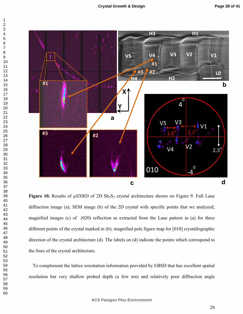
Figure 10. Results of µSXRD of 2D Sb2S3 crystal architecture shown on Figure 9. Full Laue
diffraction image (a); SEM image (b) of the 2D crystal with specific points that we analyzed;
magnified images (c) of (020) reflection as extracted from the Laue pattern in (a) for three
different points of the crystal marked in (b); magnified pole figure map for [010] crystallographic
direction of the crystal architecture (d). The labels on (d) indicate the points which correspond to
the lines of the crystal architecture.
To complement the lattice orientation information provided by EBSD that has excellent spatial
resolution but very shallow probed depth (a few nm) and relatively poor diffraction angle
H4
L0
Y
X
H3
V5 V4
H1
H2
V3 V2 V1
d
b
a
c
#1
#2 #3
#3 #2
#1
010
010 -40
40
V5
V4
V3
V2
V1
2.3o
1.8o 2.3
o
Page 28 of 41
ACS Paragon Plus Environment
Crystal Growth & Design
123456789101112131415161718192021222324252627282930313233343536373839404142434445464748495051525354555657585960

29
accuracy (typically, 1-2°), we examined the same 2D pattern of Figure 9 with µSXRD that has
much higher orientational accuracy (typically, ±0.01°), a micron size spatial resolution and probe
depths up to ~100 µm. The evolution of lattice orientation as manifested in Laue spots is shown
in Figure 10 for this 2D crystal. As an illustration, Laue spot corresponding to (020)
crystallographic planes is analyzed in detail. The diffraction from the scanned line of 2D laser-
written crystal, for instance, point #1 on Figure 10a shows a Laue spot that is steadily elongated
with a rod-like intensity distribution (Figure 10c). Similar µSXRD Laue magnified images
comprising of uniaxially elongated streaks were observed previously for 1D RLS crystal lines11
.
Such streaks were interpreted as representing unpaired randomly distributed dislocations and
their ordered assemblies like small angle grain boundaries, disclinations, etc., in the crystal. The
relative shift of the same Laue reflection for three locations #1, #2 and #3 within the same line
(see magnified images of the three points in Figure 10c) indicates the presence of lattice rotation.
It is shown systematically by the pole figure map for [010] crystallographic direction in Figure
10d from Laue data, as well as by the EBSD map in Figure 9. The much higher resolution of the
pole figure configuration by µSXRD than EBSD is very clear from a comparison of these two
figures.
As soon as the laser makes a 90o bend to form a new line (points #2 and #3 in Figure 10b), the
diffraction from this region shows a similar bend of the shape of reflection and diffuse scattering
around the reflection spot in Figure 10c. The pole figure map in Figure 10d for a part of 2D
pattern comprises three vertical segments identified as V1, V3 and V5, along with two slanted
vertical interconnections identified as V2 and V4, respectively. This map appears similar to the
pole figure map observed from EBSD for the 2D raster shown in Figure 3e. The difference
between these patterns is quantitative and qualitative. The first laser-scanned pattern formed with
Page 29 of 41
ACS Paragon Plus Environment
Crystal Growth & Design
123456789101112131415161718192021222324252627282930313233343536373839404142434445464748495051525354555657585960

30
a pitch of 7 µm in Figure 3 indicates lattice rotation of up to 37o, then the total misorientation for
the second pattern is less than 5o
(Figure 9). Note that the vertical segments of the first four lines
V1-V4 of the pattern in Figure 3e have different lengths; here the crystal lines exhibit different
average rotation rate in +x and -x scanning directions, Θ : 0.29 and 0.38°/µm for V1 and V3 and
approximately two times smaller values of 0.19 and 0.12°/µm for V2 and V4 sections. In
contrast, for the pattern with overlapping lines in Figure 10d, the length of vertical segments V1,
V3 and V5 are the same with θx=2.3° for 50 µm long crystal lines. It means that the x-
components of rotation along these lines are the same. Further, the distance between these
vertical segments indicates the y-component of rotation, θy. They are parallel to each other in
Figure 10d, which means constant y-component of rotation between these lines over their whole
length.
The behavior of segments for V2 and V4 crystal lines is fundamentally different than that of
the vertical lines V1, V3 and V5. Most obviously, the corresponding segments of PF map are not
vertical but change gradually, in contrast to those of V1, V3 and V5 lines. So the V2 and V4
lines simultaneously show rotation along x- and y-directions - vertical and horizontal directions
on the PF map in Figure 10d, respectively. Evidently these lines grow with a rotation of lattice
around an intermediate direction that is between x- and y-directions. The x-rotation is still the
same as for the odd lines, but in addition there is also an additional y-component of rotation even
though the laser is scanned in -x direction! Apparently, in these cases the crystal grows not in
exactly -x-direction but at an angle relative to the -x-scanning direction, which introduces a y-
component to the overall rotation. This observation is somewhat unexpected considering
relatively small overlapping of 1-2 microns between the lines. A rotation with y-component
implies deviation of crystal growth of line from x-scanning direction. The magnitude of this
Page 30 of 41
ACS Paragon Plus Environment
Crystal Growth & Design
123456789101112131415161718192021222324252627282930313233343536373839404142434445464748495051525354555657585960

31
component is expected to increase as the overlap with the preceding line increases, for example,
in the pattern created in Figure 8 by the ‘stitching’ protocol. The difference in the PF maps of
odd and even numbered lined in Figure 10d suggests that there are additional factors that
determine the y-component of rotation within a line.
Comparison of 2D single crystals formed by stitching and rastering protocols. It is
interesting to compare the lattice rotation that occurs in the 2D single crystals prepared by the
two methods of fabrication, viz. stitching vs. rastering. In this regard, note that lattice rotation
indicates how the amorphous structure of glass transforms into a periodic lattice of the
appropriate single crystal in the presence of stresses from density change, which vary
dynamically as the laser moves and the structure of the surrounding glass and crystal relaxes11
. In
the creation of 1D straight lines, this type of crystal growth within the confinement of a glass
matrix introduces randomly distributed unpaired dislocations and small angle grain boundaries
made of organized dislocations. The net result is a smooth rotation of the lattice along the
direction of laser scanning, as seen in Figure 2 for various straight lines. However, the situation
becomes complicated when fabricating 2D crystals. As seen in Figures 8 vs. 9 and 10, there are
both similarities and differences between the rotations in the two cases, when the lines of 2D
architectures are prepared by stitching vs. rastering protocols. In general, both processes produce
lattice rotation in both the x- and y-directions. Also, the fundamental mechanisms of crystal and
lattice rotation remain unchanged: at the end of the first and subsequent lines formed by scanning
along x-direction, the new line begins with growth along y-direction as the laser beam is moved
along y-direction. In this segment, the lattice rotates around x-direction. Thereafter, as the laser
direction is turned to move along x-direction, the rotation is determined by a combined effect of
the orientations of the preceding line and newly formed y-segment. The extent of overlap
Page 31 of 41
ACS Paragon Plus Environment
Crystal Growth & Design
123456789101112131415161718192021222324252627282930313233343536373839404142434445464748495051525354555657585960

32
between the preceding and newly forming lines, which could be different for the two protocols,
is a more explicit parameter that determines the relative values of the y component of overall
rotation of the 2D pattern.
In the case of stitching, a new dot overlapping with the previous line is formed. The orientation
of this “half dot” is controlled by the orientation at the end of the first line since it mainly grows
in y-direction and the lattice rotation follows this growth direction: the crystal lattice rotates
according to the y-component of misorientation relative to the end orientation of the previous
line. Then from this newly formed dot, as the second line is grown overlapping with the previous
line, the orientation of the lattice can follow two different scenarios, which depends on the
orientation of growth direction relative to lattice orientation. On one hand, crystal may grow in x-
direction from newly formed dot, independent of the previous line. On the other hand, the new
line can form from the preceding line via growth along some direction, which is at an angle to
the laser scanning x-direction. In both cases the new lines of 2D structure incorporate rotation in
x-direction, but under the second scenario the crystal lattice incorporates an additional y-
component of rotation. For example, this was observed for the even numbered vertical lines (V2
and V4) of the rastering pattern shown in Figures 9 and 10.
As the extent of overlap between successive lines increases, we may expect higher chances for
realizing the second growth scenario. In this context it is instructive to inspect the rotation of
crystal orientation in the 2D pattern shown on Figure 8. We examined this pattern using µSXRD
that has much higher orientational accuracy than EBSD. The resulting behavior of the 2D
crystal’s orientation is seen as its pole figure map in Figure 11 for [110] crystallographic
direction, which is close to surface normal. In this ‘stitching’ pattern four odd numbered vertical
segments (L1, L3, L5 and L7), which correspond to four crystal lines of the pattern written by
Page 32 of 41
ACS Paragon Plus Environment
Crystal Growth & Design
123456789101112131415161718192021222324252627282930313233343536373839404142434445464748495051525354555657585960

33
laser translation along +x-direction are analyzed. We note that the intensity of Laue reflections
for the three even numbered lines written in –x direction is too low to be observed on PFM. A
plausible explanation for this difference in the two types of lines is as follows: The energy band
gap for the glass matrix and Sb2S3 crystal is different: 2.0 eV and 1.5 eV, respectively. We
employed 640 nm (=1.94 eV) laser, which is a little below the bandgap of glass and significantly
larger than that of the crystal. Consequently, absorption and penetration depth of the laser beam
should be different for the two regions. For these reasons, the first crystal line would have the
largest thickness. The second line, which is made by overlapping the laser both the preceding
crystal line and glass regions would be thinner, because half of the beam would illuminate
preceding line and temperature distribution will be different than in the case of the first line. The
third line would again have a different temperature distribution then the second line with smaller
thickness than the first line, as shown schematically in Figure 12. Consequently, we observe
periodic fluctuation in the intensity of X-ray diffraction from crystal lines seen in Figure 11. We
do not observe this fluctuation of intensity in the EBSD pattern, because of the much smaller
depth probed by electrons; only the high penetration depth of X-ray beam allows the
differentiation of thickness via high and low intensities of Laue reflections from odd and even
numbered lines. Other plausible reasons for this periodic variation of diffracted intensity are:
unequal growth rates in +x and –x directions for polar Sb2S3 crystal12
, and different translations
of the movement of sample stage. Further experiments are needed to unequivocally establish the
origin of this interesting observation.
Page 33 of 41
ACS Paragon Plus Environment
Crystal Growth & Design
123456789101112131415161718192021222324252627282930313233343536373839404142434445464748495051525354555657585960

34
Figure 11. Magnified pole figure map of 2D Sb2S3 crystal architecture for [110] crystallographic
direction as obtained from µSXRD of the crystal architecture in Figure 8. The labels indicate the
points, which correspond to the lines in Figure 8.
We evaluate the orientation only of the odd numbered lines, viz. L1, L3, L5 and L7, which
were written along +x direction, due to the readily detected intensity of their Laue patterns.
Accordingly, the rotations of these four lines in x-direction have the same value of 8°. However,
the gap between the segments varies from 0.8° to 1.2°, which represents the y-component of
rotation between odd numbered lines. The other three even-numbered lines are located between
these four odd-numbered lines, so we may expect very similar rotation for them too. Overall, for
the ‘stitching’ pattern fabricated with an overlap of ~3-4 µm, evidently the crystal growth
follows second scenario, wherein the crystal lines grow from the preceding line via growth at an
angle relative to the laser scanning along x-direction. As a result, for different regions of the 2D
pattern the rotation in y-direction varies from 0.8° to 1.2°.
Y
X
110
-50
50
L1 L3 L5
L7
3.1o
8.0o
0.8o
3.9o
1.2o
Page 34 of 41
ACS Paragon Plus Environment
Crystal Growth & Design
123456789101112131415161718192021222324252627282930313233343536373839404142434445464748495051525354555657585960

35
Figure 12. Different stages of 2D RLS crystal fabrication (first and fifth line of a pattern). Note
periodic variation of the thickness of the odd and even numbered lines of laser-induced crystal as
a result of different penetration depths of the laser beam in glass and crystal regions.
With regard to the mechanism of lattice rotation, we suggest that the present 2D crystal
contains tilt dislocation walls (TDW) as in small angle grain boundaries or disclinations, and
unpaired dislocations, in analogy to 1D RLS crystal line11
. A TDW produces small abrupt
rotations (<10), while unpaired dislocations introduce gradual rotation of crystal lattice. In RLS
crystal lines these dislocations and disclinations have a line vector which is parallel to the front
of crystallization and sample surface, or in other words - normal to the laser scanning direction.
It is the same as the direction of the Frank pseudo-vector ω for disclinations or Burger vector for
dislocations. In the case of 2D crystal, the laser beam follows complex trajectory, for example,
including straight line along x-direction, and then turns to orthogonal y-direction followed by
another straight line, etc. In simple terms, the 2D crystal grows with dislocations and
disclinations, which reproduce the trajectory of laser beam and help relax interfacial stresses at
the growth front most efficiently (see Figures 8-11).
Page 35 of 41
ACS Paragon Plus Environment
Crystal Growth & Design
123456789101112131415161718192021222324252627282930313233343536373839404142434445464748495051525354555657585960

36
CONCLUSIONS
We have demonstrated the feasibility of fabricating 2D single crystal architecture from glass
by an all-solid-state single crystal growth process. Two different protocols, ‘stitching’ and
‘rastering’, were designed and tested for the fabrication of simple 2D patterns by combining
single crystal lines. The former requires new nucleation event at the end of each line and growth
only in straight line, whereas the latter starts with one nucleus and continues with a zig-zag
growth pattern. It was found for the ‘stitching’ protocol that if the step between successive lines
is larger than half the width of the crystal line, the new crystal line can have orientation different
from that of the preceding crystal line. However, if the step width is less than half the width of
the crystal line, a 2D RLS crystal is obtained. Compared to stitching, the rastering protocol
appears more promising, in which case a 2D crystal can be formed with only 1-2 µm overlap
between successive lines. For materials that may decompose/evaporate on heating, wide single
crystal lines can be made by decreasing the laser power density by increasing the laser beam
size, for instance, by shifting the focus of the laser beam a few microns above the surface of
glass sample.
For the investigated Sb2S3 crystal pattern on the surface of 16SbI3–84Sb2S3 glass, the rate of
lattice rotation is determined by the direction of laser movement relative to initial lattice
orientation. So, an appropriate choice of initial seed orientation and direction of scanning can
help minimize the rate of lattice rotation, for example, down to 5o
for a 2D pattern of 50x50 µm2
size.
All lines of 2D patterns created by both protocols demonstrate strongly correlated rotation,
which is determined by rotation of the first line. The PF maps obtained from the analysis of
Page 36 of 41
ACS Paragon Plus Environment
Crystal Growth & Design
123456789101112131415161718192021222324252627282930313233343536373839404142434445464748495051525354555657585960

37
µSXRD Laue patterns show that the rotation within all lines have a component that parallels
those in an isolated RLS crystal line. In addition, there is also an orthogonal component of
rotation, which depends on the extent of overlap between successive lines, and can be different
for the two protocols. Finally, the odd and even-numbered lines in either protocol may have
different additional orthogonal component of rotation, presumably due the difference between
optical absorption of the laser light by glass matrix and growing crystal.
AUTHOR INFORMATION
Corresponding Author
*E-mail: [email protected]
Author Contributions
D.S., V.D. and H.J. designed the overall research, and interpreted results; D.S. and C.A.
prepared the samples, designed and implemented characterization methods and analyzed results;
N.T. designed scanning Laue X-ray microdiffraction (µSXRD) setup and analyzed results; H.J.,
V.D. and D.S. wrote the paper.
Funding Sources
This work was supported by the Basic Energy Sciences Division, Department of Energy (DE-
SC0005010). C. Au-Yeung, who helped with EBSD analysis, was supported by National Science
Foundation and Lehigh University. The Advanced Light Source is supported by the Director,
Office of Science, Office of Basic Energy Sciences, Materials Sciences Division, of the U.S.
Page 37 of 41
ACS Paragon Plus Environment
Crystal Growth & Design
123456789101112131415161718192021222324252627282930313233343536373839404142434445464748495051525354555657585960

38
Department of Energy under Contract No. DE-AC02-05CH11231 at Lawrence Berkeley
National Laboratory and University of California, Berkeley, California.
Notes
The authors declare no competing financial interest.
ACKNOWLEDGEMENT
The authors thank B. Knorr for help with the laser control, and S. McAnany and C. Stan for
assistance with the µSXRD experiments.
ABBREVIATIONS
RLS crystal, Rotating lattice single crystal; EBSD, Electron Backscatter Diffraction; µSXRD,
scanning Laue X-ray microdiffraction; SCAG, single-crystal architecture in glass; CW,
Continuous Wave; fs, femtosecond; Tx, temperature of crystallization; Tm, melting temperature;
SEM, Scanning Electron Microscope; OIM, Orientation imaging microscopy; IPF, Inverse Pole
Figure; ND, Normal Direction; RD, Rolling Direction; TD, Transverse Direction; COD map,
Crystal orientation deviation map; PFM, Pole figure map; TDW, tilt dislocation walls.
REFERENCES
1. Komatsu, T., Ihara, R., Honma, T., Benino, Y., J. Am. Ceram. Soc. 2007, 90, 699-705.
2. Stone, A. et al. Sci. Rep. 2015, 5, 10391.
Page 38 of 41
ACS Paragon Plus Environment
Crystal Growth & Design
123456789101112131415161718192021222324252627282930313233343536373839404142434445464748495051525354555657585960

39
3. Fan, C., Poumellec, B., Lancry, M., He, X., Zeng, H., Erraji-Chahid, A., Liu, Q., Chen, G.
Opt. Lett. 2012, 37, 2955-2957.
4. Komatsu, T., Honma, T. J. Asian Ceram. Soc., 2013, 1 (1), 9–16.
5. Arun, P., Vedeshwar, A.G., Mehra, N.C. J. Phys. D: Appl. Phys. 1999, 32, 183–190.
6. Gupta, P., Stone, A., Woodward, N., Dierolf, V., Jain, H. Opt. Mater. Exp. 2011, 1, 652-
657.
7. Savytskii, D., Knorr, B., Dierolf, V., Jain, H. Sci. Rep., 2016, 6, 23324.
8. Honma, T., Komatsu, T. Opt. Express, 2010, 18, 8019.
9. Suzuki, F., Ogawa, K., Honma, T., Komatsu, T. J. Sol. State Chem., 2012, 185, 130-135.
10. Suzuki, F., Honma, T., Komatsu, Mater. Chem. Phys., 2011, 125, 377-381.
11. Savytskii, D., Jain, H., Tamura, N., Dierolf, V. Sci. Rep., 2016, 6, 36449.
12. Varghese, J., Barth, S., Keeney, L., Whatmore, R. W., Holmes, J. D. Nano Lett. 2012, 12,
868–872.
13. Savytskii, D., Atwater, K., Dierolf, V. and Jain, H. J. Am. Ceram. Soc., 2014, 97, 3458-
3462.
14. Savytskii, D., Knorr, B., Dierolf, V., Jain, H. J. Non-Cryst. Solids 2016, 431, 36-40.
15. Savytskii, D. Knorr, B. Dierolf, V. Jain, H. J. Non-Cryst. Solids 2013, 377, 245–249.
16. Savytskii, D., Knorr, B., Dierolf, V., Jain, H. Opt. Mater. Exp. 2013, 3, 1026-1038.
Page 39 of 41
ACS Paragon Plus Environment
Crystal Growth & Design
123456789101112131415161718192021222324252627282930313233343536373839404142434445464748495051525354555657585960

40
17. http://www.edax.com/Products/EBSD/OIM-Data-Analysis-Microstructure-Analysis.aspx
18. Kunz, M., et al. E. Rev. Sci. Instrum. 2009, 80, 035108.
19. Tamura, N. In Strain and Dislocation Gradients from Diffraction. Spatially Resolved Local
Structure and Defects; Barabash, R., Ice, G. Eds.; Imperial College Press, London, 2014; chapter
4, pp 125-155.
20. Palache, C. Berman, H. Frondel, C. In The System of Mineralogy; John Willey and Sons,
New York, ed. 7, 1944; Vol.1, pp 270-275.
21. Scavnicar, S. Z. Kristallogr. 1960, 114, 85-97.
22. Bayliss, P. Nowacki, W. Z. Kristallogr. 1972, 135, 308-315.
FOR TABLE OF CONTENTS USE ONLY:
FIGURE:
SYNOPSIS:
The nature of lattice rotation within 2D RLS crystals is established for the first time using Sb2S3
as model compound, which is fabricated on the surface of 16SbI3–84Sb2S3 glass by ‘stitching’
L3 D1
L6
L1
L5 L7
L4 L2 D3
D5 D7
D2 D4 D6
Page 40 of 41
ACS Paragon Plus Environment
Crystal Growth & Design
123456789101112131415161718192021222324252627282930313233343536373839404142434445464748495051525354555657585960

41
multiple lines or ‘rastering’ a single line. The electron back scattered diffraction mapping and
scanning Laue X-ray microdiffraction of such a 2D RLS crystal show gradual rotation of lattice
comprising of two components, one along the length of each line and another normal to this
direction.
Page 41 of 41
ACS Paragon Plus Environment
Crystal Growth & Design
123456789101112131415161718192021222324252627282930313233343536373839404142434445464748495051525354555657585960