Interface characterization and atomic intermixing processes in Be/W bilayers deposited on Si(001)...
8
Journal of Alloys and Compounds 512 (2012) 199–206 Contents lists available at SciVerse ScienceDirect Journal of Alloys and Compounds jou rn al h om epage: www.elsevier.com/locate/jallcom Interface characterization and atomic intermixing processes in Be/W bilayers deposited on Si(0 0 1) substrates with Fe buffer layers V. Kuncser a,∗ , P. Palade a , G. Schinteie a , S.G. Sandu a , L. Trupina a , G.A. Lungu a , N.G. Gheorghe a , C.M. Teodorescu a , C. Porosnicu b , I. Jepu b , C.P. Lungu b , G. Filoti a a National Institute of Materials Physics, P.O. Box MG-7, 077125, Bucharest-Magurele, Romania b National Institute for Laser, Plasma and Radiation Physics, P.O. Box MG-36, 077125, Bucharest-Magurele, Romania a r t i c l e i n f o Article history: Received 25 July 2011 Received in revised form 19 September 2011 Accepted 20 September 2011 Available online 1 October 2011 Keywords: PFCs Be/W bilayers Atomic inter-diffusion GIXRD XRR XPS CEMS a b s t r a c t Structural aspects and atomic intermixing processes in Be/W bilayers deposited on Si(0 0 1) substrates with Fe buffer layers enriched in the 57 Fe Mössbauer isotope have been studied via atomic force microscopy, grazing incidence X-ray diffractometry, X-ray reflectometry, X-ray photoelectron spec- troscopy and conversion electron Mössbauer spectroscopy. The mentioned investigations allowed a full sequential characterization of the involved interfaces. Various ionic configurations appeared for Fe or W, while an amorphous state was observed in the case of Be. It has been proven that the Be layer has a negative influence on the roughness of the whole structure, which however presents an oxidation gradient from more oxidized elements at the surface towards more reduced elements in deeper layers. A strong diffusion of the W atoms inside the Be layer, induced by the deposition method, as well as of the Fe atoms inside the Be layer, induced by thermal annealing, has been evidenced. © 2011 Elsevier B.V. All rights reserved. 1. Introduction The ambitious target of the current international programs for nuclear fusion is to demonstrate that in the next 30 years, the energy obtained by nuclear fusion can become a viable alternative from scientific, economic and safely exploitation point of view, to the needs for continuous growing energy consumptions. The envis- aged way for promoting the nuclear fusion reaction is realized via an extremely hot plasma generated in a TOKAMAK torus, e.g. as in the case of the International Thermonuclear Experimental Reactor (ITER). There are numerous important materials that must be suc- cessfully developed in order to make the thermonuclear reaction technologically viable [1,2], but, the most challenging task refers to the plasma facing components (PFCs) [3]. As it is known, in a TOKAMAK type reactor, the fusion takes place in extremely hot plasma, which is confined and kept away from the reactor walls or other material components through typical magnetic configura- tions, established by the so called limiters and diverters. In spite of the strong magnetic field confinement, the edge plasma exhausts heat and particle fluxes which finally lead to the erosion of the PFCs, ∗ Corresponding author. Fax: +40 21 3690177. E-mail addresses: kuncser@infim.ro, [email protected] (V. Kuncser). by physical sputtering, chemical erosion or melting/sublimation, all these phenomena reducing the life time of the PFCs. On the other hand, the eroded atom-like impurities from the PFCs can migrate into the plasma core with negative influence on the fusion per- formances. Taking into account all the above mentioned aspects, the materials designed for the PFCs should have outstanding per- formances with respect to their thermo-mechanical properties, erosion yield, fuel retention capability, insignificant influence on the fusion performances and reduced activation. Unfortunately, the above requirements cannot be fulfilled by just one type of material, but by two distinct categories, each one with enhanced performances with respect to a complementary part of the require- ments. Light elements, such as C or Be, with a low impact on the core plasma performances, have significant erosion yields whereas heavy elements such as W have a low erosion yield but can degrade strongly the plasma performances. Therefore, reduced activation Fe–9%Cr ferritic/martensitic steels and SiC/ceramic SiC composites covered by Be and/or W layers, in well defined sequences, can be considered for different PFCs. It is worth mentioning that another effect, related to the plasma wall interaction, consists in the fact that the sputtered atoms from PFCs can reach critical points of other components, as improper mixed compounds, which might affect their own performances. Hence, the knowledge of the atomic intermixing process and the related effect on structural and thermal properties of thin films and multilayers involving typical elements 0925-8388/$ – see front matter © 2011 Elsevier B.V. All rights reserved. doi:10.1016/j.jallcom.2011.09.063
-
Upload
independent -
Category
Documents
-
view
1 -
download
0
Transcript of Interface characterization and atomic intermixing processes in Be/W bilayers deposited on Si(001)...
Id
VNa
b
a
ARR1AA
KPBAXXC
1
neftaat(
cttTpotth
0d
Journal of Alloys and Compounds 512 (2012) 199– 206
Contents lists available at SciVerse ScienceDirect
Journal of Alloys and Compounds
jou rn al h om epage: www.elsev ier .com/ locate / ja l l com
nterface characterization and atomic intermixing processes in Be/W bilayerseposited on Si(0 0 1) substrates with Fe buffer layers
. Kuncsera,∗, P. Paladea, G. Schinteiea, S.G. Sandua, L. Trupinaa, G.A. Lungua,.G. Gheorghea, C.M. Teodorescua, C. Porosnicub, I. Jepub, C.P. Lungub, G. Filoti a
National Institute of Materials Physics, P.O. Box MG-7, 077125, Bucharest-Magurele, RomaniaNational Institute for Laser, Plasma and Radiation Physics, P.O. Box MG-36, 077125, Bucharest-Magurele, Romania
r t i c l e i n f o
rticle history:eceived 25 July 2011eceived in revised form9 September 2011ccepted 20 September 2011vailable online 1 October 2011
a b s t r a c t
Structural aspects and atomic intermixing processes in Be/W bilayers deposited on Si(0 0 1) substrateswith Fe buffer layers enriched in the 57Fe Mössbauer isotope have been studied via atomic forcemicroscopy, grazing incidence X-ray diffractometry, X-ray reflectometry, X-ray photoelectron spec-troscopy and conversion electron Mössbauer spectroscopy. The mentioned investigations allowed a fullsequential characterization of the involved interfaces. Various ionic configurations appeared for Fe or W,while an amorphous state was observed in the case of Be.
eywords:FCse/W bilayerstomic inter-diffusion GIXRDRRPS
It has been proven that the Be layer has a negative influence on the roughness of the whole structure,which however presents an oxidation gradient from more oxidized elements at the surface towards morereduced elements in deeper layers. A strong diffusion of the W atoms inside the Be layer, induced by thedeposition method, as well as of the Fe atoms inside the Be layer, induced by thermal annealing, has beenevidenced.
© 2011 Elsevier B.V. All rights reserved.
EMS. Introduction
The ambitious target of the current international programs foruclear fusion is to demonstrate that in the next 30 years, thenergy obtained by nuclear fusion can become a viable alternativerom scientific, economic and safely exploitation point of view, tohe needs for continuous growing energy consumptions. The envis-ged way for promoting the nuclear fusion reaction is realized vian extremely hot plasma generated in a TOKAMAK torus, e.g. as inhe case of the International Thermonuclear Experimental ReactorITER).
There are numerous important materials that must be suc-essfully developed in order to make the thermonuclear reactionechnologically viable [1,2], but, the most challenging task referso the plasma facing components (PFCs) [3]. As it is known, in aOKAMAK type reactor, the fusion takes place in extremely hotlasma, which is confined and kept away from the reactor wallsr other material components through typical magnetic configura-
ions, established by the so called limiters and diverters. In spite ofhe strong magnetic field confinement, the edge plasma exhaustseat and particle fluxes which finally lead to the erosion of the PFCs,∗ Corresponding author. Fax: +40 21 3690177.E-mail addresses: [email protected], [email protected] (V. Kuncser).
925-8388/$ – see front matter © 2011 Elsevier B.V. All rights reserved.oi:10.1016/j.jallcom.2011.09.063
by physical sputtering, chemical erosion or melting/sublimation, allthese phenomena reducing the life time of the PFCs. On the otherhand, the eroded atom-like impurities from the PFCs can migrateinto the plasma core with negative influence on the fusion per-formances. Taking into account all the above mentioned aspects,the materials designed for the PFCs should have outstanding per-formances with respect to their thermo-mechanical properties,erosion yield, fuel retention capability, insignificant influence onthe fusion performances and reduced activation. Unfortunately,the above requirements cannot be fulfilled by just one type ofmaterial, but by two distinct categories, each one with enhancedperformances with respect to a complementary part of the require-ments. Light elements, such as C or Be, with a low impact on thecore plasma performances, have significant erosion yields whereasheavy elements such as W have a low erosion yield but can degradestrongly the plasma performances. Therefore, reduced activationFe–9%Cr ferritic/martensitic steels and SiC/ceramic SiC compositescovered by Be and/or W layers, in well defined sequences, can beconsidered for different PFCs. It is worth mentioning that anothereffect, related to the plasma wall interaction, consists in the factthat the sputtered atoms from PFCs can reach critical points of
other components, as improper mixed compounds, which mightaffect their own performances. Hence, the knowledge of the atomicintermixing process and the related effect on structural and thermalproperties of thin films and multilayers involving typical elements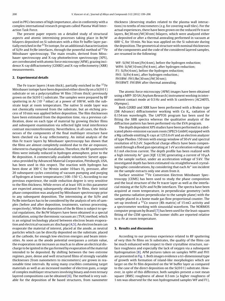
2 s and
uca
abtoMbadm
2
MsgssnchiacnbttifiBrhb2optaptFprciitepastcirtsmola
00 V. Kuncser et al. / Journal of Alloy
sed in PFCs becomes of high importance, also in conformity with aomplex international research program called Plasma Wall Inter-ction Task Force.
The present paper reports on a detailed study of structuralspects and atomic intermixing processes taking place in Be/Wilayers deposited on Si substrates with a thin Fe buffer layer par-ially enriched in the 57Fe isotope, for an additional characterizationf Si/Fe and Fe/Be interfaces, through the powerful method of 57Feössbauer spectroscopy. The main results, derived from Möss-
auer spectroscopy and X-ray photoelectron spectroscopy (XPS),re corroborated with atomic force microscopy (AFM), grazing inci-ence X-ray diffractometry (GIXRD) and X-ray reflectometry (XRR)easurements.
. Experimental details
The Fe tracer layers (4 nm thick), partially enriched in the 57Feössbauer isotope have been deposited either directly on a Si(0 0 1)
ubstrate or on a polycrystalline W film (10 nm thick) previouslyrown on the Si(0 0 1) substrate. The samples were prepared by RFputtering in Ar (10−2 mbar) at a power of 100 W, with the sub-trate kept at room temperature. The native Si oxide layer wasot chemically removed from the substrate, but an etching pro-ess of 10 min was applied before deposition. The film thicknessesave been estimated from the deposition time, via a previous cal-
bration, done on each type of material by growing thicker filmsnd subsequent examination via reflected light total interferenceontrast microinterferometry. Nevertheless, in all cases, the thick-esses of the components of the final multilayer structure haveeen checked via X-ray reflectometry. An initial analysis of thehin Fe tracer layers by Mössbauer spectroscopy has shown thathe films are almost completely oxidized due to the air exposure,nherent to changing the installation. Therefore, the RF sputtered Felms were initially reduced in hydrogen atmosphere, prior to thee deposition. A commercially available volumetric Sievert appa-atus provided by Advanced Material Corporation, Pittsburgh, USA,as been used in this respect. The reaction with hydrogen haseen done at 300 ◦C for 90 min under 10 bars H2 pressure, after0 subsequent cycles consisting of vacuum pumping and purgingf hydrogen at lower temperatures (100–150 ◦C). According to ourrevious experience, the oxide reduction degree is very sensitiveo the film thickness. While errors of at least 10% in this parameterre expected among subsequently obtained Fe films, their initialhase composition was analyzed by Mössbauer spectroscopy prioro any subsequent deposition. The intermixing at the Si/Fe ande/Be interfaces has to be considered by the analysis of sets of sam-les (before and after deposition, treatments, various processing,espectively). While the deposition of the Be films is subject to spe-ial regulations, the Be/W bilayers have been obtained in a specialnstallation, using the thermionic vacuum arc (TVA) method, whichs an original technology placed between electron beam evapora-ion and electrical vacuum arc discharge [4,5]. An electron beam canvaporate the material of interest, placed at the anode, as neutralarticles which can be directly deposited on the substrate, placedt the cathode, for enough low electron energies and beam inten-ities. As soon as the anode potential overpasses a certain value,he evaporation rate increases as much as to allow an electrical dis-harge to be ignited in the gas formed by evaporation of the materialntended to be deposited. By shifting between the two extremeegimes, pure, dense and well structured films of strongly variablehicknesses (from nanometers to micrometers) are grown in rea-onable time intervals. By using many crucibles containing target
aterials as well as an increased number of electron guns, a rangef complex multilayer structures involving binary and even ternaryayered compositions can be obtained [6]. The method is very suit-ble for the deposition of Be based structures, from nanometer
Compounds 512 (2012) 199– 206
thickness (deserving studies related to the plasma wall interac-tions) to tenths of micrometers (e.g. for covering wall tiles). For theactual experiences, there have been grown on the reduced Fe tracerlayers, Be(30 nm)/W(30 nm) bilayers, which were analyzed eitheras deposited or after a thermal annealing performed in vacuum at600 ◦C, for 10 min. No bias was applied on the Si substrate duringthe deposition. The geometrical structure with nominal thicknessesof the components and the code of the considered layered samples,are resumed in the following:
WF: Si/W(10 nm)/Fe(4 nm), before the hydrogen reduction;WFH: Si/W(10 nm)/Fe(4 nm), after hydrogen reduction;F1: Si/Fe(4 nm), before the hydrogen reduction;FH1: Si/Fe(4 nm), after hydrogen reduction.;FH1BW: FH1/Be(30 nm)/W(30 nm);FH1BWT: FH1BW after thermal annealing.
The atomic force microscopy (AFM) images have been obtainedusing a MFP-3D SA (Asylum Research) instrument working in inter-mittent contact mode at 0.5 Hz and with Si cantilevers (AC240TS,Olympus).
Both GIXRD and XRR have been performed with a Bruker type(D8 Advance) diffractometer working with Cu K� radiation of0.154 nm wavelength. The LAPTOS program has been used forfitting the XRR spectra whereas the qualitative analysis of thediffraction pattern has been performed via the EVA program.
The depth dependent XPS studies have been performed in a ded-icated photo-emission vacuum room (SPECS GmbH) equipped witha Mg cathode emitting X-rays at 1253.6 eV and an electron analyzerof type Phoibos 150 mm with energy window of 50 eV and spectralresolution of 0.2 eV. Superficial charge effects have been compen-sated through a flood gun operating at 1 eV acceleration voltage and0.1 mA electron current. The depth profile has been realized witha high intensity Ar+ gun (IQE 12/38) generating a current of 10 �Aat the sample surface, under an acceleration voltage of 5 kV. Theinvestigated depth has been estimated via straightforward crystal-lographic considerations, by considering that each Ar+ ion incidenton the sample extracts only one atom from it.
Surface sensitive 57Fe Conversion Electron Mössbauer Spec-troscopy (CEMS) has been used to study the phase compositionand the local structure of the Fe tracer layer as well as the interfa-cial mixing at the Si/Fe and Fe/Be interfaces. The spectra have beenacquired at room temperature, in perpendicular geometry (withthe gamma radiation perpendicular to the sample plane) with thesample placed in a home made gas flow proportional counter. Theset-up involved a 57Co source (Rh matrix) of 15 mCi activity anda spectrometer working with sinusoidal waveform. The NORMOScomputer program by Brand [7] has been used for the least-squaresfitting of the CEM spectra. The isomer shifts are reported relativeto �-Fe at room temperature.
3. Results and discussion
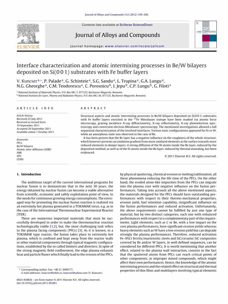
According to our previous experience related to RF sputteringof very thin Fe films on Si substrates, the quality of the films canbe much enhanced with respect to their crystalline structure, sur-face roughness and especially the lack of oxygen via a subsequenthydrogenation [8]. AFM pictures taken on samples WFH and FH1are presented in Fig. 1. Both images evidence a tri-dimensional typeof growth with formation of island-like morphologies which arelarger on the Fe film deposited on the W buffer layer as compared
to the case of the direct deposition on the Si(0 0 1) substrate. How-ever, in spite of this difference, both samples present a root meansquare (RMS) roughness of about 0.5 nm (a higher roughness of1 nm was observed for the non hydrogenated samples WF and F1),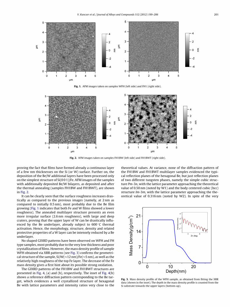
V. Kuncser et al. / Journal of Alloys and Compounds 512 (2012) 199– 206 201
Fig. 1. AFM images taken on samples WFH (left side) and FH1 (right side).
FH1BW
podowti
tcgrmceapu
tcWcrm
psgB
value of 0.50 nm (noted by W1) and the body centered cubic (bcc)structure Im-3m, with the lattice parameter approaching the the-oretical value of 0.316 nm (noted by W2). In spite of the very
0 10 200
7
14
21
3 6
e-13
e-9
e-5
e-1
2θ (deg)
Inte
nsity(c
ou
nts
)
Ma
ss D
en
sity(g
/cm
3)
Fig. 2. AFM images taken on samples
roving the fact that films have formed already a continuous layerf a few nm thicknesses on the Si (or W) surface. Further on, theeposition of the Be/W additional layers have been processed onlyn the simplest structure of Si(0 0 1)/Fe. AFM images of the samplesith additionally deposited Be/W bilayers, as deposited and after
he thermal annealing (samples FH1BW and FH1BWT), are shownn Fig. 2.
It can be clearly seen that the surface roughness increases dras-ically as compared to the previous images (namely, at 2 nm asompared to initially 0.5 nm), most probably due to the Be filmrowing (Fig. 1 indicates that both Fe and W films showed a loweroughness). The annealed multilayer structure presents an evenore irregular surface (2.6 nm roughness), with large and deep
raters, proving that the upper layer of W can be drastically influ-nced by the Be underlayer, already subject to 600 ◦C thermalctivation. Hence, the morphology, structure, density and relatedrotective properties of a W layer can be intensely reduced by a Benderlayer.
No shaped GIXRD patterns have been observed on WFH and FHype samples, most probably due to the very low thickness and poorrystallization of films. However, the mass density profile of sample
FH obtained via XRR patterns (see Fig. 3) confirms the geometri-al structure of the sample, Si/W(≈12 nm)/Fe(≈5 nm), as well as theelatively high roughness of the top Fe layer. The decrease of the Feass density gives a first hint about its possible strong oxidation.The GIXRD patterns of the FH1BW and FH1BWT structures are
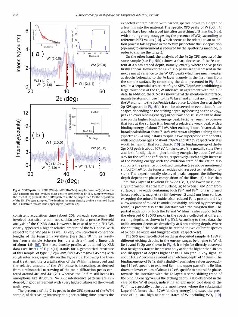
resented in Fig. 4, (a) and (b), respectively. The inset of Fig. 4(b)hows a reference diffraction pattern corresponding to the Be tar-et, which evidences a well crystallized structure of hexagonale with lattice parameters and intensity ratios very close to the
(left side) and FH1BWT (right side).
theoretical values. At variance, none of the diffraction pattern ofthe FH1BW and FH1BWT multilayer samples evidenced the typi-cal reflection planes of the hexagonal Be, but just reflection planesof two different tungsten phases, namely the simple cubic struc-ture Pm-3n, with the lattice parameter approaching the theoretical
Depth(nm)
Fig. 3. Mass density profile of the WFH sample, as obtained from fitting the XRRdata (shown in the inset). The depth in the mass density profile is counted from theSi substrate towards the upper layers (bottom-up).
202 V. Kuncser et al. / Journal of Alloys and
20 40 600
2
4
6
W2 (2,0,0)
2 4 6
e-12
e-8
e-4
e0
2θ (degree)
Inte
nsi
ty(c
ounts
)
0 20 40 60 80 10 00
5
10
15
20
Depth(nm )
Ma
ss D
ensity(g
/cm
3)
W1(2,0,0)
W2 (1,1,0)W1 (2,1,1)W1 (2,1,0)
Inte
nsity(c
ou
nts
)
2θ (deg)
( a )
20 40 60
0
3
6
9
12
40 600
300
600
900
Be (0,0,2)
Be (1,0,1)
Be (1,0,0)
Inte
nsity(c
ou
nts
)
2θ (deg)
W1 (2,0,0)
( b )
W2 ( 2,0,0)
W2 ( 1,1,0)W1 (2,1,1)W1 (2,1,0)
Inte
nsity(c
ou
nts
)
2θ (de g)
Fig. 4. GIXRD patterns of FH1BW (a) and FH1BWT (b) samples. Insets of (a) show theXRR patterns and the involved mass density profile of the FH1BW sample whereasthe inset of (b) presents the GIXRD pattern of the Be target used for the depositionot
ciacrliodormtftadm
s
case of the W 4f peaks, indicating an enhanced oxidation of the
f the FH1BW type samples. The depth in the mass density profile is counted fromhe Si substrate towards the upper layers (bottom-up).
onsistent acquisition time (about 20 h on each spectrum), thenvolved statistics remain not satisfactory for a precise Rietveldnalysis of the GIXRD data. However, in case of sample FH1BW,learly appeared a higher relative amount of the W1 phase withespect to the W2 phase as well as very low structural coherenceengths of the tungsten crystallites (less than 10 nm, as result-ng from a simple Scherrer formula with k = 1 and a linewidthf about 1.5◦ [9]). The mass density profile, as obtained by XRRata (see insets of Fig. 4(a)) stands for a geometrical structuref this sample, of type Si/Fe(≈5 nm)/Be(≈45 nm)/W(≈45 nm) withough interfaces, especially on the Fe/Be side. Following the ther-al treatment, the crystallization of the W film is improved and
he relative amount of the W1 phase is increasing, as derivedrom a substantial narrowing of the main diffraction peaks cen-ered around 40◦ and 44◦ (2�), whereas the Be film still keeps itsmorphous like structure. No XRR interference patterns are evi-enced, in good agreement with a very high roughness of the overall
ultilayer.The presence of the C 1s peaks in the XPS spectra of the WFHample, of decreasing intensity at higher etching time, proves the
Compounds 512 (2012) 199– 206
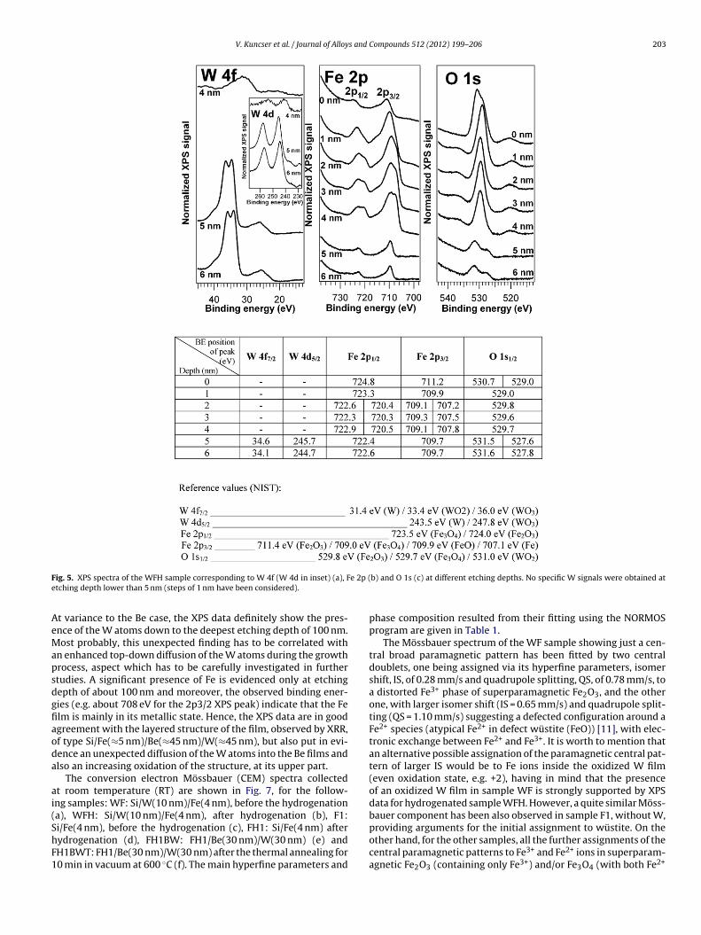
expected contamination with carbon species down to a depth ofa few nm into the material. The specific XPS peaks of W (both 4fand 4d) have been observed just after an etching of 5 nm (Fig. 5(a)),with binding energies suggesting the presence of WO2, according toreference NIST values [10], which seems to be related to an oxida-tion process taking place in the W film just before the Fe deposition(opening to environment is required by the sputtering machine, inorder to change the target).
On the other hand, the analysis of the Fe 2p XPS spectra of thesame sample (see Fig. 5(b)) shows a sharp decrease of the Fe con-tent at a 5 nm etched depth, namely, exactly where the W peaksfirstly appear. However the Fe 2p XPS peaks are still present in thenext 2 nm at variance to the W XPS peaks which are much weakerat depths belonging to the Fe layer, namely in the first 4 nm fromthe sample surface. By combining the data presented in Fig. 5, itresults a sequential structure of type Si/W/Fe(≈5 nm) exhibiting alarge roughness at the Fe/W interface, in agreement with the XRRdata. In addition, the XPS data show that at the mentioned interface,mainly Fe atoms diffuse into the W layer and almost no diffusion ofthe W atoms into the bcc Fe side takes place. Looking closer at the Fe2p XPS spectra in Fig. 5(b), it can be observed an evolution of theirshapes, depending on the etching depth. By focusing on the Fe 2p3/2peak at lower binding energy (an equivalent discussion can be donealso on the higher binding energy peak, Fe 2p1/2), one may observethat just at the surface it is formed a relatively weak peak with abinding energy of about 711 eV. After etching 1 nm of material, thebroad peak shifts at about 710 eV whereas at a higher etching depth(spectra at 2–4 nm) it starts to split in two superposed components,with binding energies of about 709 eV and 707 eV respectively. It isworth to mention that according to [10] the binding energy of the Fe2p3 XPS peak is about 707 eV for the case of the metallic state (Fe0)and it shifts slightly at higher binding energies by about 2 eV and4 eV for the Fe2+ and Fe3+ states, respectively. Such a slight increaseof the binding energy with the oxidation state of the cation alsosupports the presence of oxidized tungsten (see above mentionedshift of 2–4 eV for the tungsten oxides with respect to metallic tung-sten). The experimentally observed peaks support the followingdepth dependent phase composition of the films: (i) a less than1 nm thick layer of trivalent Fe oxide (Fe2O3) of lower mass den-sity is formed just at the film surface, (ii) between 1 and 2 nm fromsurface, an Fe oxide containing both Fe2+ and Fe3+ ions is formed(most probably, magnetite), (iii) between 2 and 5 nm from surface,excepting the mixed Fe oxide, also reduced Fe is present and (iv)a low amount of mixed Fe oxide (inevitably induced by processingroute) is present also at the interface with the tungsten film. Thepartial oxidation of both the Fe and W films is also supported bythe observed O 1s XPS peaks in the spectra collected at differentetching depths, as shown in Fig. 5(c). According to these data, theoxide amount decreases drastically at 5 nm etching depth, wherethe splitting of the peak might be related to two different speciesof oxides (Fe oxide and tungsten oxide, respectively).
The XPS spectra collected on the as deposited sample FH1BW atdifferent etching depths, in the energy ranges belonging to W 4f,Be 1s and Fe 2p are shown in Fig. 6. It might be directly observedthat Be signals start to be present only at depths higher than 40 nmand disappear at depths higher than 90 nm (the Si 2p3 signal atabout 100 eV becomes evident at an etching depth of 110 nm). Thebinding energy of Be 1s, shifts slightly from higher values approach-ing 114 eV, specific to oxidized Be in the upper part of the Be film,down to lower values of about 112 eV, specific to neutral Be phase,towards the interface with the Fe layer. A same shifting trend ofthe binding energy versus the etching depth is also observed in the
W films, especially at the outermost layers, where the substantiallarge shift (more than 37 eV binding energy) indicates the pres-ence of unusual high oxidation states of W, including WO3 [10].
V. Kuncser et al. / Journal of Alloys and Compounds 512 (2012) 199– 206 203
F e 2p (e
AeMapsdgfiaoda
ai(ShF1
ig. 5. XPS spectra of the WFH sample corresponding to W 4f (W 4d in inset) (a), Ftching depth lower than 5 nm (steps of 1 nm have been considered).
t variance to the Be case, the XPS data definitely show the pres-nce of the W atoms down to the deepest etching depth of 100 nm.ost probably, this unexpected finding has to be correlated with
n enhanced top-down diffusion of the W atoms during the growthrocess, aspect which has to be carefully investigated in furthertudies. A significant presence of Fe is evidenced only at etchingepth of about 100 nm and moreover, the observed binding ener-ies (e.g. about 708 eV for the 2p3/2 XPS peak) indicate that the Felm is mainly in its metallic state. Hence, the XPS data are in goodgreement with the layered structure of the film, observed by XRR,f type Si/Fe(≈5 nm)/Be(≈45 nm)/W(≈45 nm), but also put in evi-ence an unexpected diffusion of the W atoms into the Be films andlso an increasing oxidation of the structure, at its upper part.
The conversion electron Mössbauer (CEM) spectra collectedt room temperature (RT) are shown in Fig. 7, for the follow-ng samples: WF: Si/W(10 nm)/Fe(4 nm), before the hydrogenationa), WFH: Si/W(10 nm)/Fe(4 nm), after hydrogenation (b), F1:
i/Fe(4 nm), before the hydrogenation (c), FH1: Si/Fe(4 nm) afterydrogenation (d), FH1BW: FH1/Be(30 nm)/W(30 nm) (e) andH1BWT: FH1/Be(30 nm)/W(30 nm) after the thermal annealing for0 min in vacuum at 600 ◦C (f). The main hyperfine parameters andb) and O 1s (c) at different etching depths. No specific W signals were obtained at
phase composition resulted from their fitting using the NORMOSprogram are given in Table 1.
The Mössbauer spectrum of the WF sample showing just a cen-tral broad paramagnetic pattern has been fitted by two centraldoublets, one being assigned via its hyperfine parameters, isomershift, IS, of 0.28 mm/s and quadrupole splitting, QS, of 0.78 mm/s, toa distorted Fe3+ phase of superparamagnetic Fe2O3, and the otherone, with larger isomer shift (IS = 0.65 mm/s) and quadrupole split-ting (QS = 1.10 mm/s) suggesting a defected configuration around aFe2+ species (atypical Fe2+ in defect wüstite (FeO)) [11], with elec-tronic exchange between Fe2+ and Fe3+. It is worth to mention thatan alternative possible assignation of the paramagnetic central pat-tern of larger IS would be to Fe ions inside the oxidized W film(even oxidation state, e.g. +2), having in mind that the presenceof an oxidized W film in sample WF is strongly supported by XPSdata for hydrogenated sample WFH. However, a quite similar Möss-bauer component has been also observed in sample F1, without W,
providing arguments for the initial assignment to wüstite. On theother hand, for the other samples, all the further assignments of thecentral paramagnetic patterns to Fe3+ and Fe2+ ions in superparam-agnetic Fe2O3 (containing only Fe3+) and/or Fe3O4 (with both Fe2+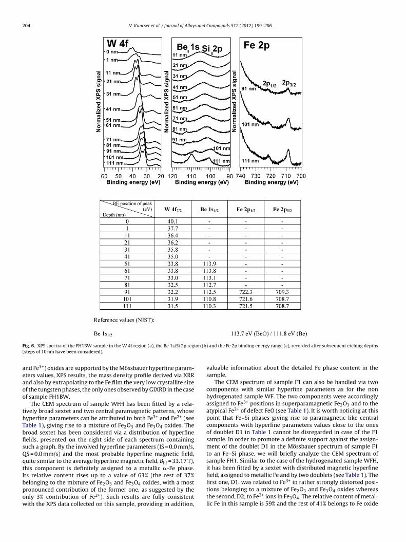
204 V. Kuncser et al. / Journal of Alloys and Compounds 512 (2012) 199– 206
F ion (b(
aeaoo
thTbfisQqtIbpow
ig. 6. XPS spectra of the FH1BW sample in the W 4f region (a), the Be 1s/Si 2p regsteps of 10 nm have been considered).
nd Fe3+) oxides are supported by the Mössbauer hyperfine param-ters values, XPS results, the mass density profile derived via XRRnd also by extrapolating to the Fe film the very low crystallite sizef the tungsten phases, the only ones observed by GIXRD in the casef sample FH1BW.
The CEM spectrum of sample WFH has been fitted by a rela-ively broad sextet and two central paramagnetic patterns, whoseyperfine parameters can be attributed to both Fe3+ and Fe2+ (seeable 1), giving rise to a mixture of Fe2O3 and Fe3O4 oxides. Theroad sextet has been considered via a distribution of hyperfineelds, presented on the right side of each spectrum containinguch a graph. By the involved hyperfine parameters (IS = 0.0 mm/s,S = 0.0 mm/s) and the most probable hyperfine magnetic field,uite similar to the average hyperfine magnetic field, Bhf = 33.17 T),his component is definitely assigned to a metallic �-Fe phase.ts relative content rises up to a value of 63% (the rest of 37%
elonging to the mixture of Fe2O3 and Fe3O4 oxides, with a mostronounced contribution of the former one, as suggested by thenly 3% contribution of Fe2+). Such results are fully consistentith the XPS data collected on this sample, providing in addition,) and the Fe 2p binding energy range (c), recorded after subsequent etching depths
valuable information about the detailed Fe phase content in thesample.
The CEM spectrum of sample F1 can also be handled via twocomponents with similar hyperfine parameters as for the nonhydrogenated sample WF. The two components were accordinglyassigned to Fe3+ positions in superparamagnetic Fe2O3 and to theatypical Fe2+ of defect FeO (see Table 1). It is worth noticing at thispoint that Fe–Si phases giving rise to paramagnetic like centralcomponents with hyperfine parameters values close to the onesof doublet D1 in Table 1 cannot be disregarded in case of the F1sample. In order to promote a definite support against the assign-ment of the doublet D1 in the Mössbauer spectrum of sample F1to an Fe–Si phase, we will briefly analyze the CEM spectrum ofsample FH1. Similar to the case of the hydrogenated sample WFH,it has been fitted by a sextet with distributed magnetic hyperfinefield, assigned to metallic Fe and by two doublets (see Table 1). The
first one, D1, was related to Fe3+ in rather strongly distorted posi-tions belonging to a mixture of Fe2O3 and Fe3O4 oxides whereasthe second, D2, to Fe2+ ions in Fe3O4. The relative content of metal-lic Fe in this sample is 59% and the rest of 41% belongs to Fe oxide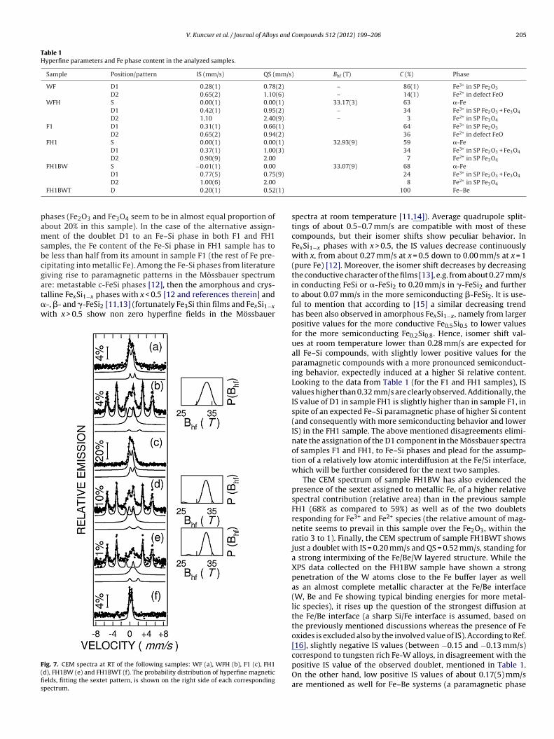
V. Kuncser et al. / Journal of Alloys and Compounds 512 (2012) 199– 206 205
Table 1Hyperfine parameters and Fe phase content in the analyzed samples.
Sample Position/pattern IS (mm/s) QS (mm/s) Bhf (T) C (%) Phase
WF D1 0.28(1) 0.78(2) – 86(1) Fe3+ in SP Fe2O3
D2 0.65(2) 1.10(6) – 14(1) Fe2+ in defect FeOWFH S 0.00(1) 0.00(1) 33.17(3) 63 �-Fe
D1 0.42(1) 0.95(2) – 34 Fe3+ in SP Fe2O3 + Fe3O4
D2 1.10 2.40(9) – 3 Fe2+ in SP Fe3O4
F1 D1 0.31(1) 0.66(1) 64 Fe3+ in SP Fe2O3
D2 0.65(2) 0.94(2) 36 Fe2+ in defect FeOFH1 S 0.00(1) 0.00(1) 32.93(9) 59 �-Fe
D1 0.37(1) 1.00(3) 34 Fe3+ in SP Fe2O3 + Fe3O4
D2 0.90(9) 2.00 7 Fe2+ in SP Fe3O4
FH1BW S −0.01(1) 0.00 33.07(9) 68 �-FeD1 0.77(5) 0.75(9) 24 Fe3+ in SP Fe2O3 + Fe3O4
(1)
pamsbcgat�w
F(fis
D2 1.00(6) 2.00FH1BWT D 0.20(1) 0.52
hases (Fe2O3 and Fe3O4 seem to be in almost equal proportion ofbout 20% in this sample). In the case of the alternative assign-ent of the doublet D1 to an Fe–Si phase in both F1 and FH1
amples, the Fe content of the Fe-Si phase in FH1 sample has toe less than half from its amount in sample F1 (the rest of Fe pre-ipitating into metallic Fe). Among the Fe-Si phases from literatureiving rise to paramagnetic patterns in the Mössbauer spectrum
re: metastable c-FeSi phases [12], then the amorphous and crys-alline FexSi1−x phases with x < 0.5 [12 and references therein] and-, �- and �-FeSi2 [11,13] (fortunately Fe3Si thin films and FexSi1−xith x > 0.5 show non zero hyperfine fields in the Mössbauerig. 7. CEM spectra at RT of the following samples: WF (a), WFH (b), F1 (c), FH1d), FH1BW (e) and FH1BWT (f). The probability distribution of hyperfine magneticelds, fitting the sextet pattern, is shown on the right side of each correspondingpectrum.
8 Fe2+ in SP Fe3O4
100 Fe–Be
spectra at room temperature [11,14]). Average quadrupole split-tings of about 0.5–0.7 mm/s are compatible with most of thesecompounds, but their isomer shifts show peculiar behavior. InFexSi1−x phases with x > 0.5, the IS values decrease continuouslywith x, from about 0.27 mm/s at x = 0.5 down to 0.00 mm/s at x = 1(pure Fe) [12]. Moreover, the isomer shift decreases by decreasingthe conductive character of the films [13], e.g. from about 0.27 mm/sin conducting FeSi or �-FeSi2 to 0.20 mm/s in �-FeSi2 and furtherto about 0.07 mm/s in the more semiconducting �-FeSi2. It is use-ful to mention that according to [15] a similar decreasing trendhas been also observed in amorphous FexSi1−x, namely from largerpositive values for the more conductive Fe0.5Si0.5 to lower valuesfor the more semiconducting Fe0.2Si0.8. Hence, isomer shift val-ues at room temperature lower than 0.28 mm/s are expected forall Fe–Si compounds, with slightly lower positive values for theparamagnetic compounds with a more pronounced semiconduct-ing behavior, expectedly induced at a higher Si relative content.Looking to the data from Table 1 (for the F1 and FH1 samples), ISvalues higher than 0.32 mm/s are clearly observed. Additionally, theIS value of D1 in sample FH1 is slightly higher than in sample F1, inspite of an expected Fe–Si paramagnetic phase of higher Si content(and consequently with more semiconducting behavior and lowerIS) in the FH1 sample. The above mentioned disagreements elimi-nate the assignation of the D1 component in the Mössbauer spectraof samples F1 and FH1, to Fe–Si phases and plead for the assump-tion of a relatively low atomic interdiffusion at the Fe/Si interface,which will be further considered for the next two samples.
The CEM spectrum of sample FH1BW has also evidenced thepresence of the sextet assigned to metallic Fe, of a higher relativespectral contribution (relative area) than in the previous sampleFH1 (68% as compared to 59%) as well as of the two doubletsresponding for Fe3+ and Fe2+ species (the relative amount of mag-netite seems to prevail in this sample over the Fe2O3, within theratio 3 to 1). Finally, the CEM spectrum of sample FH1BWT showsjust a doublet with IS = 0.20 mm/s and QS = 0.52 mm/s, standing fora strong intermixing of the Fe/Be/W layered structure. While theXPS data collected on the FH1BW sample have shown a strongpenetration of the W atoms close to the Fe buffer layer as wellas an almost complete metallic character at the Fe/Be interface(W, Be and Fe showing typical binding energies for more metal-lic species), it rises up the question of the strongest diffusion atthe Fe/Be interface (a sharp Si/Fe interface is assumed, based onthe previously mentioned discussions whereas the presence of Feoxides is excluded also by the involved value of IS). According to Ref.[16], slightly negative IS values (between −0.15 and −0.13 mm/s)
correspond to tungsten rich Fe-W alloys, in disagreement with thepositive IS value of the observed doublet, mentioned in Table 1.On the other hand, low positive IS values of about 0.17(5) mm/sare mentioned as well for Fe–Be systems (a paramagnetic phase
2 s and
adaS
4
vdrmbvuawd
vSrtwaWicbccefwwdo
[
[
[
[
[
06 V. Kuncser et al. / Journal of Alloy
ppears for Be concentrations exceeding 75%) [17]. Hence, theata from Table 1 are consistent with a strong diffusion of the Fetoms inside the Be layer, induced by the thermal treatments of thei/Fe/Be/W multilayers annealed for 10 min at 600 ◦C.
. Conclusions
The investigation of multi-layer interface behavior was realizedia Fe buffer layers enriched in the 57Fe Mössbauer isotope grownirectly on Si(0 0 1) substrates or on thin W underlayers. A partialeduction of the films has been obtained via their subsequent treat-ent in hydrogen atmosphere. Be(30 nm)/W(30 nm) bilayers have
een grown on the hydrogenated Fe tracer layers, via a thermionicacuum arc method and a thermal treatment, performed in vac-um, at 600 ◦C for 10 min was subsequently applied. All structuresppearing in various processing stages, have been characterizedith respect to morphological–structural, phase composition andiffusion aspects, via AFM, GIXRD, XRR, XPS and CEMS.
The gradual investigation of the processed samples has pro-ided relevant information. The surface roughness of the as growni/Fe/Be/W structure increases drastically as compared to theoughness of the initial hydrogenated Si/Fe structure. Annealingreatments induced an even higher roughness of the structure,ith large and deep craters, proving that the Be underlayer has
negative influence on the quality/density/adherence of the upper layer. Excepting the about 40 nm thick W layer, all the other
nvolved layers of the analyzed structures have shown a poorrystallization and almost short range order. Two W phases haveeen evidenced by GIXRD in the Si/Fe/Be/W system, their relativeontent depending on the annealing conditions. However, theiroherence length is very low (nm range) suggesting that the coher-nce lengths and crystallization degree have to be even loweror the rest of the structure components. XPS data are consistent
ith a high surface oxidation, even for the hydrogenated systems,here a higher reduction of the elements is observed mainly in theeeper layers. A strong diffusion of the W atoms into the Be layer isbserved for the as prepared Si/Fe/B/W system, where Mössbauer[
[
[
Compounds 512 (2012) 199– 206
spectra are consistent with a sharp Fe/Si interface and the presenceof still oxidized Fe superparamagnetic phases (mainly magnetite)along the Fe film. At variance, annealing treatments remove theoxygen from the Fe/Be interface, but induce a strong diffusion ofthe Fe atoms into the Be layer.
Acknowledgements
The financial support through the Romanian National ProgramIDEI, project number PN2-IDEI 1382/2008 and project number BS-M-5-EUROATOM is highly acknowledged.
References
[1] S.J. Zinkle, Fusion Eng. Des. 74 (2005) 31–40.[2] E.E. Bloom, S.J. Zinkle, F.W. Wiffen, J. Nuclear Mater. 329–333 (2004) 12–19.[3] Fusion News, Newsletter, vol. 3, 2009, ISSN 1818-5355.[4] C.P. Lungu, I. Mustata, G. Musa, V. Zaroschi, A.M. Lungu, K. Iwasaki, Vacuum 76
(2004) 127.[5] V. Kuncser, I. Mustata, C.P. Lungu, A.M. Lungu, V. Zaroschi, W. Keune, B. Sahoo,
F. Stromberg, M. Walterfang, L. Ion, G. Filoti, Surf. Coat. Technol. 200 (2005)980.
[6] V. Kuncser, G. Schinteie, P. Palade, I. Jepu, I. Mustata, C.P. Lungu, F. Miculescu,G. Filoti, J. Alloys Compd. 499 (2010) 23–29.
[7] R.A. Brand, Nuclear Instrum. Method Phys. Res. B 28 (1987) 398.[8] V. Kuncser, F. Tolea, G. Schinteie, I. Jepu, P. Palade, Digest J. Nanomater.
Biostruct. 6 (1) (2011) 199–206.[9] C. Suryanarayana, M. Grant Norton, X-ray Diffraction; A Practical Approach,
Plenum Press, New York, 1998.10] http://srdata.nist.gov/xps/selEnergyType.aspx;
http://www.lasurface.com/database/spectrexps.php.11] N.N. Greenwood, T.C. Gibb, Mössbauer Spectroscopy, Chapmann and Hall, Lon-
don, 1971.12] M. Walterfang, W. Keune, K. Trunov, R. Peters, U. Rucker, K. Westerholt, Phys.
Rev. B 73 (2006) 214423.13] J. Desimoni, F.H. Sanchez, M.B. Fernandez van Raap, H. Bernas, C. Clerc, X.W.
Lin, Phys. Rev. B 51 (1) (1995) 86–90.14] K. Trunov, M. Walterfang, W. Keune, N.K. Utochkina, A. Trunova, Thin Solid
Films 516 (2008) 6205–6209.
15] F.H. Sanchez, M.B. Fernandez van Raap, J. Desimoni, Phys. Rev. B 44 (1991)4290.16] G. Le Caer, P. Delcroix, T.D. Shen, B. Malaman, Phys. Rev. B 54 (18) (1996)
12775–12786.17] O. Keizo, J. Appl. Phys. 39 (4) (1968) 2123–2126.