Interactions of defect complexes and domain walls in CuO-doped ferroelectric (K,Na)NbO3
6
Interactions of defect complexes and domain walls in CuO-doped ferroelectric (K,Na)NbO3 Rüdiger-A. Eichel, Ebru Erünal, Peter Jakes, Sabine Körbel, Christian Elsässer et al. Citation: Appl. Phys. Lett. 102, 242908 (2013); doi: 10.1063/1.4811268 View online: http://dx.doi.org/10.1063/1.4811268 View Table of Contents: http://apl.aip.org/resource/1/APPLAB/v102/i24 Published by the AIP Publishing LLC. Additional information on Appl. Phys. Lett. Journal Homepage: http://apl.aip.org/ Journal Information: http://apl.aip.org/about/about_the_journal Top downloads: http://apl.aip.org/features/most_downloaded Information for Authors: http://apl.aip.org/authors Downloaded 03 Oct 2013 to 202.116.1.149. This article is copyrighted as indicated in the abstract. Reuse of AIP content is subject to the terms at: http://apl.aip.org/about/rights_and_permissions
-
Upload
independent -
Category
Documents
-
view
5 -
download
0
Transcript of Interactions of defect complexes and domain walls in CuO-doped ferroelectric (K,Na)NbO3
Interactions of defect complexes and domain walls in CuO-dopedferroelectric (K,Na)NbO3Rüdiger-A. Eichel, Ebru Erünal, Peter Jakes, Sabine Körbel, Christian Elsässer et al. Citation: Appl. Phys. Lett. 102, 242908 (2013); doi: 10.1063/1.4811268 View online: http://dx.doi.org/10.1063/1.4811268 View Table of Contents: http://apl.aip.org/resource/1/APPLAB/v102/i24 Published by the AIP Publishing LLC. Additional information on Appl. Phys. Lett.Journal Homepage: http://apl.aip.org/ Journal Information: http://apl.aip.org/about/about_the_journal Top downloads: http://apl.aip.org/features/most_downloaded Information for Authors: http://apl.aip.org/authors
Downloaded 03 Oct 2013 to 202.116.1.149. This article is copyrighted as indicated in the abstract. Reuse of AIP content is subject to the terms at: http://apl.aip.org/about/rights_and_permissions
Interactions of defect complexes and domain walls in CuO-dopedferroelectric (K,Na)NbO3
R€udiger-A. Eichel,1,a) Ebru Er€unal,2 Peter Jakes,1 Sabine K€orbel,3 Christian Els€asser,3
Hans Kungl,1,4 J�erome Acker,4,b) and Michael J. Hoffmann4
1Forschungszentrum J€ulich, Institut f€ur Energie- und Klimaforschung (IEK-9), D-52425 J€ulich, Germany2Institut f€ur Physikalische Chemie, Universit€at Freiburg, Albertstr. 21, D-79104 Freiburg, Germany3Fraunhofer-Institut f€ur Werkstoffmechanik IWM, W€ohlerstr. 11, D-79108 Freiburg, Germany4Karlsruher Institut f€ur Technologie (KIT), Institut f€ur Angewandte Materialien-Keramik im Maschinenbau(IAM-KM), D-76131 Karlsruhe, Germany
(Received 17 March 2013; accepted 30 May 2013; published online 19 June 2013)
“Lead-free” piezoelectric sodium potassium niobate has been studied with respect to its defect
structure when doping with CuO. The results indicate that two kinds of mutually compensating
charged defect complexes are formed, ðCu000Nb � V••OÞ0 and ðV••
O � Cu000Nb � V••OÞ
•. Concerning the
interplay of these defect complexes with the piezoelectric materials properties, the trimeric
ðV••O � Cu000Nb � V••
OÞ•
defect complex primarily has an elastic dipole moment and thus is proposed to
impact the electromechanical properties, whereas the dimeric ðCu000Nb � V••OÞ0 defect possesses an
electric dipole moment in addition to an elastic distortion. Both types of defect complexes can impede
domain-wall motion and may contribute to ferroelectric “hardening.” VC 2013 AIP Publishing LLC.
[http://dx.doi.org/10.1063/1.4811268]
Point defects and defect complexes play an important
role to tailor functional materials. In ferroelectrics, which
allow to convert mechanical to electrical energy and vice-
versa, for applications ranging from medical imaging to non-
volatile memories, electro-mechanical sensors, transducers
or actuators, “hard” or “soft” behavior critically depends on
the nature of point defects. Particularly dimeric defect com-
plexes between acceptor-type dopant ions and charge-
compensating oxygen vacancies have pronounced impact on
the properties of these materials. By exploiting the electric
and elastic properties associated with these defect dipoles,1
their interaction with the domain structure and domain walls
is discussed in terms of materials hardening,1 aging,1,2 and
electrical fatigue.3,4 It has been shown recently for Mn-
doped barium titanate single crystals that the behavior of di-
meric ðMn00Ti � V••OÞ�
defect dipoles explains the underlying
mechanism of high electro-mechanical strain in terms of a
symmetry-conforming short-range ordering principle
between defect complexes and ferroelectric domains.2
Motivated by environmental concerns because of the tox-
icity of lead oxide current research focuses on the search for
“lead-free” alternatives to the widely used Pb[Zr1�xTix]O3
(PZT) solid-solution system which show comparable
performance.5–8 Promising alternatives are modified alkali
niobates ([KyNa1�y]NbO3, KNN) and solid solutions between
bismuth sodium titanate and barium titanate (BNT-BT) with a
composition close to a morphotropic phase boundary.9,10
KNN ceramics modified with Li, Ta, or Sb have been reported
to exhibit suitable piezoelectric properties for actuator applica-
tions at ambient temperature.11 However, the main difference
between PZT and lead-free ferroelectrics manifests itself in
the fact that PZT with small chemical modifications is a robust
multi-purpose piezoelectric material, whereas for the presently
known lead-free compounds variations in composition are
mandatory to tailor properties for specific applications.8
In respect to the defect structure, the mechanisms of
charge compensation when considering acceptor doping with
aliovalent ions on perovskite B-sites are expected to consider-
ably differ between PZT, BNT-BT, and KNN. Whereas in
the two former cases the B-site ion is tetravalent (Ti4þ, Zr4þ),
for KNN it is pentavalent (Nb5þ). As consequence the inves-
tigated mechanism of compensating the excess charge associ-
ated with an Cu2þ-acceptor dopant with one oxygen vacancy
by formation of a charge neutral ðCu00Ti � V••OÞ�
defect com-
plex,12 cannot directly be transferred to Cu2þ-doped KNN. It
is hence of significant interest to understand the origin of
modified materials properties on an atomic scale. Concerning
CuO-doped KNN, an enhanced mechanical quality factor Qm
and a hardening has recently been reported,13–15 whereby the
question has remained unanswered what is the kind of defect
structure and how this impacts the domain structure.
KNN 50/50 containing 0.25 mol. % Cu, (K0.5Na0.5)
(Nb0.9975Cu0.0025)O2.99625, was prepared by a mixed oxide-
carbonate route.35,36 K2CO3, Na2CO3, Nb2O5, and CuO were
mixed by attrition milling in isopropanol, dried, sieved, and
calcined at 775 8C for 5 h. After final ball milling, drying and
sieving, pellets were formed by uniaxial and cold isostatic
pressing at 500 MPa. Sintering at 1105 8C for 2 h resulted in
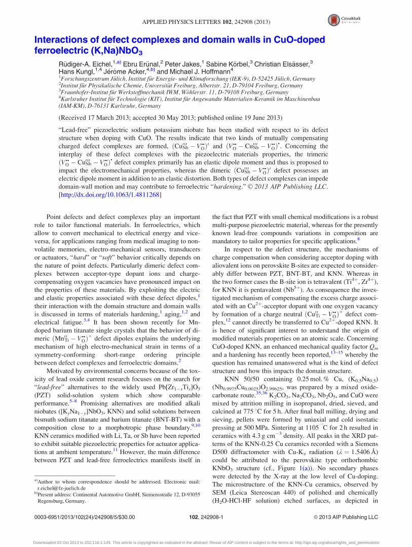
ceramics with 4.3 g cm�3 density. All peaks in the XRD pat-
terns of the KNN-0.25 Cu ceramics recorded with a Siemens
D500 diffractometer with Cu-Ka radiation (k ¼ 1:5406 A)
could be attributed to the perovskite type orthorhombic
KNbO3 structure (cf., Figure 1(a)). No secondary phases
were detected by the X-ray at the low level of Cu-doping.
The microstructure of the KNN-Cu ceramics, observed by
SEM (Leica Stereoscan 440) of polished and chemically
(H2O-HCl-HF solution) etched surfaces, as depicted in
a)Author to whom correspondence should be addressed. Electronic mail:
[email protected])Present address: Continental Automotive GmbH, Siemensstraße 12, D-93055
Regensburg, Germany.
0003-6951/2013/102(24)/242908/5/$30.00 VC 2013 AIP Publishing LLC102, 242908-1
APPLIED PHYSICS LETTERS 102, 242908 (2013)
Downloaded 03 Oct 2013 to 202.116.1.149. This article is copyrighted as indicated in the abstract. Reuse of AIP content is subject to the terms at: http://apl.aip.org/about/rights_and_permissions
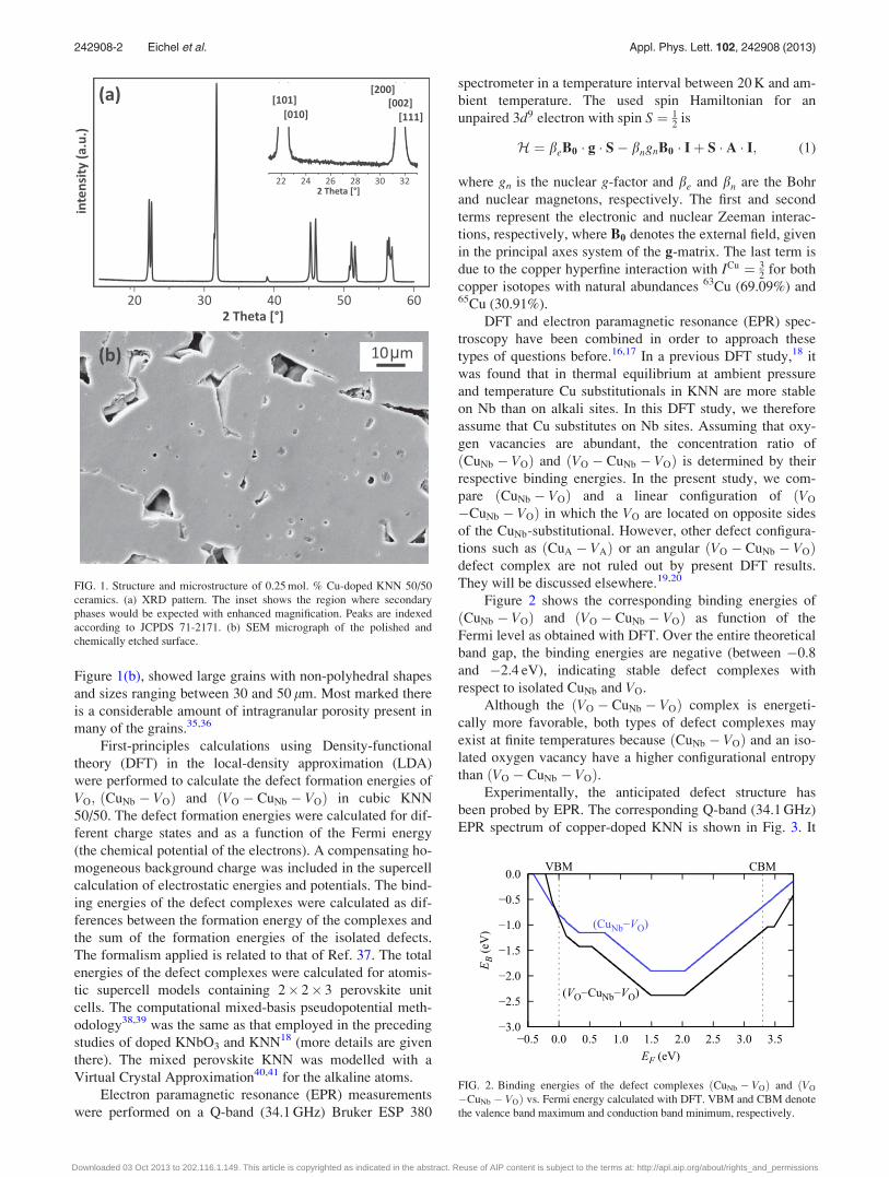
Figure 1(b), showed large grains with non-polyhedral shapes
and sizes ranging between 30 and 50 lm. Most marked there
is a considerable amount of intragranular porosity present in
many of the grains.35,36
First-principles calculations using Density-functional
theory (DFT) in the local-density approximation (LDA)
were performed to calculate the defect formation energies of
VO; ðCuNb � VOÞ and ðVO � CuNb � VOÞ in cubic KNN
50/50. The defect formation energies were calculated for dif-
ferent charge states and as a function of the Fermi energy
(the chemical potential of the electrons). A compensating ho-
mogeneous background charge was included in the supercell
calculation of electrostatic energies and potentials. The bind-
ing energies of the defect complexes were calculated as dif-
ferences between the formation energy of the complexes and
the sum of the formation energies of the isolated defects.
The formalism applied is related to that of Ref. 37. The total
energies of the defect complexes were calculated for atomis-
tic supercell models containing 2� 2� 3 perovskite unit
cells. The computational mixed-basis pseudopotential meth-
odology38,39 was the same as that employed in the preceding
studies of doped KNbO3 and KNN18 (more details are given
there). The mixed perovskite KNN was modelled with a
Virtual Crystal Approximation40,41 for the alkaline atoms.
Electron paramagnetic resonance (EPR) measurements
were performed on a Q-band (34.1 GHz) Bruker ESP 380
spectrometer in a temperature interval between 20 K and am-
bient temperature. The used spin Hamiltonian for an
unpaired 3d9 electron with spin S ¼ 12
is
H ¼ beB0 � g � S� bngnB0 � Iþ S � A � I; (1)
where gn is the nuclear g-factor and be and bn are the Bohr
and nuclear magnetons, respectively. The first and second
terms represent the electronic and nuclear Zeeman interac-
tions, respectively, where B0 denotes the external field, given
in the principal axes system of the g-matrix. The last term is
due to the copper hyperfine interaction with ICu ¼ 32
for both
copper isotopes with natural abundances 63Cu (69.09%) and65Cu (30.91%).
DFT and electron paramagnetic resonance (EPR) spec-
troscopy have been combined in order to approach these
types of questions before.16,17 In a previous DFT study,18 it
was found that in thermal equilibrium at ambient pressure
and temperature Cu substitutionals in KNN are more stable
on Nb than on alkali sites. In this DFT study, we therefore
assume that Cu substitutes on Nb sites. Assuming that oxy-
gen vacancies are abundant, the concentration ratio of
ðCuNb � VOÞ and ðVO � CuNb � VOÞ is determined by their
respective binding energies. In the present study, we com-
pare ðCuNb � VOÞ and a linear configuration of ðVO
�CuNb � VOÞ in which the VO are located on opposite sides
of the CuNb-substitutional. However, other defect configura-
tions such as ðCuA � VAÞ or an angular ðVO � CuNb � VOÞdefect complex are not ruled out by present DFT results.
They will be discussed elsewhere.19,20
Figure 2 shows the corresponding binding energies of
ðCuNb � VOÞ and ðVO � CuNb � VOÞ as function of the
Fermi level as obtained with DFT. Over the entire theoretical
band gap, the binding energies are negative (between �0.8
and �2.4 eV), indicating stable defect complexes with
respect to isolated CuNb and VO.
Although the ðVO � CuNb � VOÞ complex is energeti-
cally more favorable, both types of defect complexes may
exist at finite temperatures because ðCuNb � VOÞ and an iso-
lated oxygen vacancy have a higher configurational entropy
than ðVO � CuNb � VOÞ.Experimentally, the anticipated defect structure has
been probed by EPR. The corresponding Q-band (34.1 GHz)
EPR spectrum of copper-doped KNN is shown in Fig. 3. It
FIG. 1. Structure and microstructure of 0.25 mol. % Cu-doped KNN 50/50
ceramics. (a) XRD pattern. The inset shows the region where secondary
phases would be expected with enhanced magnification. Peaks are indexed
according to JCPDS 71-2171. (b) SEM micrograph of the polished and
chemically etched surface.
FIG. 2. Binding energies of the defect complexes ðCuNb � VOÞ and ðVO
�CuNb � VOÞ vs. Fermi energy calculated with DFT. VBM and CBM denote
the valence band maximum and conduction band minimum, respectively.
242908-2 Eichel et al. Appl. Phys. Lett. 102, 242908 (2013)
Downloaded 03 Oct 2013 to 202.116.1.149. This article is copyrighted as indicated in the abstract. Reuse of AIP content is subject to the terms at: http://apl.aip.org/about/rights_and_permissions
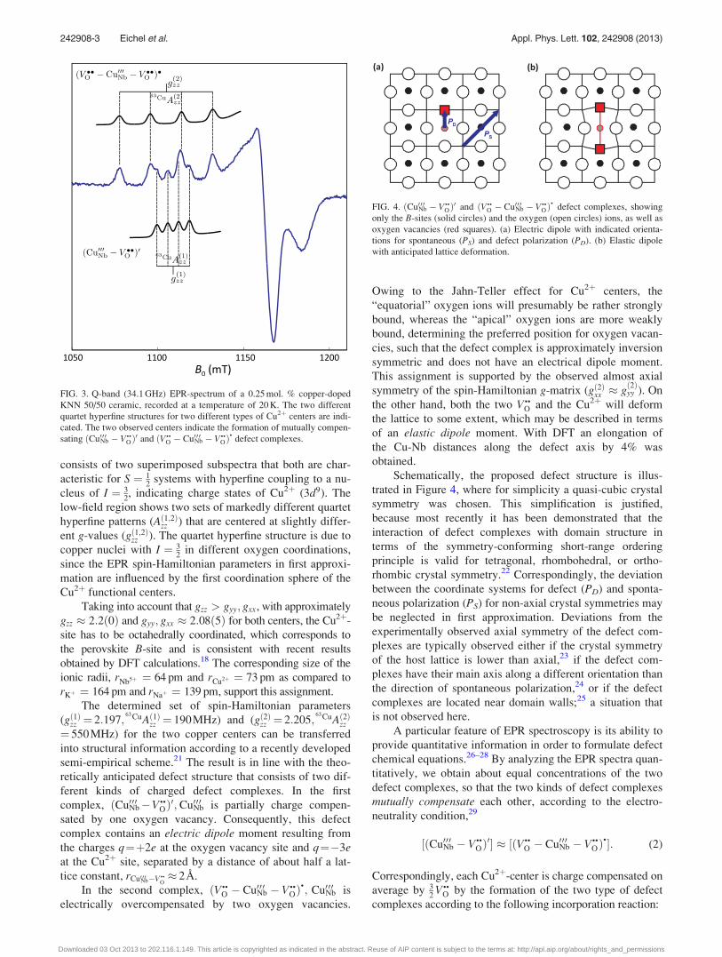
consists of two superimposed subspectra that both are char-
acteristic for S ¼ 12
systems with hyperfine coupling to a nu-
cleus of I ¼ 32, indicating charge states of Cu2þ (3d9). The
low-field region shows two sets of markedly different quartet
hyperfine patterns (Að1;2Þzz ) that are centered at slightly differ-
ent g-values (gð1;2Þzz ). The quartet hyperfine structure is due to
copper nuclei with I ¼ 32
in different oxygen coordinations,
since the EPR spin-Hamiltonian parameters in first approxi-
mation are influenced by the first coordination sphere of the
Cu2þ functional centers.
Taking into account that gzz > gyy; gxx, with approximately
gzz � 2:2ð0Þ and gyy; gxx � 2:08ð5Þ for both centers, the Cu2þ-
site has to be octahedrally coordinated, which corresponds to
the perovskite B-site and is consistent with recent results
obtained by DFT calculations.18 The corresponding size of the
ionic radii, rNb5þ ¼ 64 pm and rCu2þ ¼ 73 pm as compared to
rKþ ¼ 164 pm and rNaþ ¼ 139 pm, support this assignment.
The determined set of spin-Hamiltonian parameters
(gð1Þzz ¼ 2:197;63CuAð1Þzz ¼ 190MHz) and (gð2Þzz ¼ 2:205;
63CuAð2Þzz
¼ 550MHz) for the two copper centers can be transferred
into structural information according to a recently developed
semi-empirical scheme.21 The result is in line with the theo-
retically anticipated defect structure that consists of two dif-
ferent kinds of charged defect complexes. In the first
complex, ðCu000Nb�V••OÞ0; Cu000Nb is partially charge compen-
sated by one oxygen vacancy. Consequently, this defect
complex contains an electric dipole moment resulting from
the charges q¼þ2e at the oxygen vacancy site and q¼�3eat the Cu2þ site, separated by a distance of about half a lat-
tice constant, rCu0 0 0Nb�V••O� 2A.
In the second complex, ðV••O � Cu000Nb � V••
OÞ•; Cu000Nb is
electrically overcompensated by two oxygen vacancies.
Owing to the Jahn-Teller effect for Cu2þ centers, the
“equatorial” oxygen ions will presumably be rather strongly
bound, whereas the “apical” oxygen ions are more weakly
bound, determining the preferred position for oxygen vacan-
cies, such that the defect complex is approximately inversion
symmetric and does not have an electrical dipole moment.
This assignment is supported by the observed almost axial
symmetry of the spin-Hamiltonian g-matrix (gð2Þxx � gð2Þyy ). On
the other hand, both the two V••O and the Cu2þ will deform
the lattice to some extent, which may be described in terms
of an elastic dipole moment. With DFT an elongation of
the Cu-Nb distances along the defect axis by 4% was
obtained.
Schematically, the proposed defect structure is illus-
trated in Figure 4, where for simplicity a quasi-cubic crystal
symmetry was chosen. This simplification is justified,
because most recently it has been demonstrated that the
interaction of defect complexes with domain structure in
terms of the symmetry-conforming short-range ordering
principle is valid for tetragonal, rhombohedral, or ortho-
rhombic crystal symmetry.22 Correspondingly, the deviation
between the coordinate systems for defect (PD) and sponta-
neous polarization (PS) for non-axial crystal symmetries may
be neglected in first approximation. Deviations from the
experimentally observed axial symmetry of the defect com-
plexes are typically observed either if the crystal symmetry
of the host lattice is lower than axial,23 if the defect com-
plexes have their main axis along a different orientation than
the direction of spontaneous polarization,24 or if the defect
complexes are located near domain walls;25 a situation that
is not observed here.
A particular feature of EPR spectroscopy is its ability to
provide quantitative information in order to formulate defect
chemical equations.26–28 By analyzing the EPR spectra quan-
titatively, we obtain about equal concentrations of the two
defect complexes, so that the two kinds of defect complexes
mutually compensate each other, according to the electro-
neutrality condition,29
½ðCu000Nb � V••OÞ0� � ½ðV••
O � Cu000Nb � V••OÞ
•�: (2)
Correspondingly, each Cu2þ-center is charge compensated on
average by 32
V••O by the formation of the two type of defect
complexes according to the following incorporation reaction:
FIG. 3. Q-band (34.1 GHz) EPR-spectrum of a 0.25 mol. % copper-doped
KNN 50/50 ceramic, recorded at a temperature of 20 K. The two different
quartet hyperfine structures for two different types of Cu2þ centers are indi-
cated. The two observed centers indicate the formation of mutually compen-
sating ðCu0 0 0Nb � V••OÞ0 and ðV••
O � Cu0 0 0Nb � V••OÞ
•defect complexes.
FIG. 4. ðCu0 0 0Nb � V••OÞ0 and ðV••
O � Cu0 0 0Nb � V••OÞ
•defect complexes, showing
only the B-sites (solid circles) and the oxygen (open circles) ions, as well as
oxygen vacancies (red squares). (a) Electric dipole with indicated orienta-
tions for spontaneous (PS) and defect polarization (PD). (b) Elastic dipole
with anticipated lattice deformation.
242908-3 Eichel et al. Appl. Phys. Lett. 102, 242908 (2013)
Downloaded 03 Oct 2013 to 202.116.1.149. This article is copyrighted as indicated in the abstract. Reuse of AIP content is subject to the terms at: http://apl.aip.org/about/rights_and_permissions
K2CO3 þ Na2CO3 þ Nb2O5 þ 2CuO
�!KNN ðV••O � Cu000Nb � V••
OÞ•
þðCu000Nb � V••OÞ0 þ O2ðgÞ þ 2COðgÞ
þ 2K�K þ 2Na�Na þ 2Nb�Nb þ 9O�O : (3)
CuO-doped KNN compounds thus exhibit a pronoun-
cedly different defect structure as compared to doped PZT
or BaTiO3, for which it is well established that acceptor ions
in general form dimeric defect complexes with an electric
dipole moment;30–33 trimeric complexes such as the
ðV••O � Cu000Nb � V••
OÞ•
that presumably exhibit mainly elastic
distortions are absent in PZT and BaTiO3. Furthermore, local
differences in the nature of chemical bonding between the
Cu2þ-functional center and its coordinated ions were
recently reported.34
Because dimeric defect complexes were shown to reor-
ient under an applied external field,42 and assuming the tri-
meric might be reoriented under sufficiently strong field as
well, the piezoelectric properties of CuO-doped KNN com-
pounds can be interpreted on an atomic scale as follows:
recently it has been reported that CuO-doped KNN exhibits
markedly enhanced mechanical quality factors.13–15 The
interaction of the ðV••O � Cu000Nb � V••
OÞ•
defect complex with
two types of domain walls is schematically illustrated in
Figure 5. In Figure 5(a), the ferroelectric strain is perpendic-
ular to the defect-induced local strain on the right side of the
domain wall. A movement of the domain wall to the left
increases the elastic energy unless the defect complex rotates
as depicted in Figure 5(a). This effect does not occur for the
configuration depicted in Figure 5(b), where ferroelectric
and defect-induced local strains are parallel on both sides of
the domain wall. Owing to the reorientation of the
ðV••O � Cu000Nb � V••
OÞ•
defect complex, as described for the
mechanism in Figure 5(a), the oxygen vacancies have to
migrate around the Cu2þ functional center. Because this pro-
cess involves a hopping of two oxygen vacancies a consider-
ably high amount of energy is needed, such that an effective
pinning of domain walls may be provided.1
In summary, “lead-free” piezoelectric sodium potassium
niobate has been studied with respect to its defect structure
when doping with CuO. The results indicate that two kinds
of mutually compensating charged defect complexes are
formed, ðCu000Nb � V••OÞ0 and ðV••
O � Cu000Nb � V••OÞ
•, similar to
the situation for the pure members of the KNN solid solution
system.43,44 In particular, a trimeric defect complex has been
identified that defines a point of departure to explore electro-
mechanical properties in lead-free ferroelectrics. The tri-
meric ðV••O � Cu000Nb � V••
OÞ•
defect complex primarily has an
elastic dipole moment, whereas the dimeric ðCu000Nb � V••OÞ0
defect possesses an electric dipole moment in addition to an
elastic distortion. Both types of defect complexes can
impede domain-wall motion and may contribute to ferroelec-
tric “hardening.”
This research has been financially supported by the DFG
through the projects EI 498/1-2, EL 155/21-2, and HO 1165/
14-2.
1U. Robels and G. Arlt, J. Appl. Phys. 73, 3454–3460 (1993).2X. Ren, Nature Mater. 3, 91–94 (2004).3S. P€oykk€o and D. J. Chadi, Phys. Rev. Lett. 83, 1231–1234 (1999).4J. F. Scott and M. Dawber, Appl. Phys. Lett. 76, 3801–3803 (2000).5L. E. Cross, Nature 432, 24–25 (2004).6J. R€odel, W. Jo, K. T. P. Seifert, E. M. Anton, T. Granzow, and D.
Damjanovic, J. Am. Ceram. Soc. 92, 1153–1177 (2009).7R.-A. Eichel and H. Kungl, Funct. Mater. Lett. 3, 1–4 (2010).8D. Damjanovic, N. Klein, J. Li, and V. Porokhonskyy, Funct. Mater. Lett.
3, 5–13 (2010).9T. Takenaka and H. Nagata, J. Eur. Ceram. Soc. 25, 2693–2700 (2005).
10M. Kosec, B. Malic, A. Bencan, T. Rojac, and J. Tellier, Funct. Mater.
Lett. 3, 15–18 (2010).11Y. Saito, H. Takao, T. Tani, T. Nonoyama, K. Takatori, T. Homma, T.
Nagaya, and M. Nakamura, Nature 432, 84–87 (2004).12R.-A. Eichel, P. Erhart, P. Tr€askelin, K. Albe, H. Kungl, and M. J.
Hoffmann, Phys. Rev. Lett. 100, 095504 (2008).13M. Matsubara, T. Yamaguchi, K. Kikuta, and S. Hirano, Jpn. J. Appl.
Phys. Part 1 43, 7159–7163 (2004).14E. Li, H. Kakemoto, S. Wada, and T. Tsurumi, IEEE Trans. Ultrason.
Ferroelectr. Freq. Control 55, 980–987 (2008).15F. Azough, M. Wegrzyn, R. Freer, S. Sharma, and D. Hall, J. Eur. Ceram.
Soc. 31, 569–576 (2011).16R.-A. Eichel, J. Am. Ceram. Soc. 91, 691–701 (2008).17R.-A. Eichel, H. Kungl, and P. Jakes, Mater. Technol. (2013) doi:10.1179/
175355513X13715615193120.18S. K€orbel, P. Marton, and C. Els€asser, Phys. Rev. B 81, 174115 (2010).19S. K€orbel, “Atomistic modeling of Cu doping in the lead-free ferroelectric
potassium sodium niobate,” PhD dissertation, http://www.freidok.uni-frei-
burg.de/volltexte/8860.20S. K€orbel and C. Els€asser, “Alignment of ferroelectric polarization and
defect complexes in copper-doped potassium niobate,” Phys. Rev. B
(submitted).21R.-A. Eichel, M. D. Drahus, P. Jakes, E. Er€unal, E. Erdem, S. K. S.
Parashar, H. Kungl, and M. J. Hoffmann, Mol. Phys. 107, 1981–1986
(2009).22Z. Feng and X. Ren, Phys. Rev. B 77, 134115 (2008).23E. Aksel, E. Erdem, P. Jakes, J. L. Jones, and R.-A. Eichel, Appl. Phys.
Lett. 97, 012903 (2010).24E. Erdem, R.-A. Eichel, H. Kungl, M. J. Hoffmann, A. Ozarowski, J. van
Tol, and L. C. Brunel, Phys. Scr. T 129, 12–16 (2007).25P. Jakes, E. Erdem, R.-A. Eichel, L. Jin, and D. Damjanovic, Appl. Phys.
Lett. 98, 072907 (2011).26E. Erdem, P. Jakes, S. K. S. Parashar, K. Kiraz, M. Somer, A. R€udiger,
and R.-A. Eichel, J. Phys.: Condens. Matter 22, 345901 (2010) .27E. Aksel, P. Jakes, E. Erdem, D. M. Smyth, A. Ozarowski, J. van Tol, J. L.
Jones, and R.-A. Eichel, J. Am. Ceram. Soc. 94, 1363–1367 (2011).28M. D. Drahus, P. Jakes, E. Erdem, and R.-A. Eichel, Solid State Ionics
184, 47–51 (2011).
FIG. 5. Interaction between the ðV••O � Cu0 0 0Nb � V••
OÞ•
defect complex with two
types of domain walls. The orientation of spontaneous polarization is repre-
sented by a bold blue arrow. (a) Ferroelectric and defect-induced strain parallel
on one side of the domain wall and perpendicular on the other. (b) Ferroelectric
and defect-induced strain parallel on both sides of the domain wall.
242908-4 Eichel et al. Appl. Phys. Lett. 102, 242908 (2013)
Downloaded 03 Oct 2013 to 202.116.1.149. This article is copyrighted as indicated in the abstract. Reuse of AIP content is subject to the terms at: http://apl.aip.org/about/rights_and_permissions
29D. M. Smyth, The Defect Chemistry of Metal Oxides (Oxford University
Press, New York, 2000).30K. A. M€uller, W. Berlinger, and J. Albers, Phys. Rev. B 32, 5837
(1985).31W. L. Warren, G. E. Pike, K. Vanheusden, D. Dimos, B. A. Tuttle, and J.
Robertson, J. Appl. Phys. 79, 9250 (1996).32H. Me�stric, R.-A. Eichel, T. Kloss, K.-P. Dinse, So. Laubach, St. Laubach,
and P. C. Schmidt, Phys. Rev. B 71, 134109 (2005).33E. Erdem, P. Jakes, R.-A. Eichel, D. C. Sinclair, M. Pasha, and I. M.
Reaney, Funct. Mater. Lett. 3, 65–68 (2010).34R.-A. Eichel, E. Er€unal, M. D. Drahus, D. M. Smyth, J. van Tol, J. Acker,
H. Kungl, and M. J. Hoffmann, Phys. Chem. Chem. Phys. 11, 8698–8705
(2009).35J. Acker, H. Kungl, and M. J. Hoffmann, J. Am. Ceram. Soc. 93,
1270–1281 (2010).
36J. Acker, H. Kungl, and M. J. Hoffmann, J. Eur. Ceram. Soc. 33,
2127–2139 (2013).37P. Erhart and K. Albe, J. Appl. Phys. 102, 084111 (2007).38C. Els€asser, N. Takeuchi, K. M. Ho, C. T. Chan, P. Braun, and M. F€ahnle,
J. Phys. Condens. Matter 2, 4371 (1990).39F. Lechermann, F. Welsch, C. Els€asser, C. Ederer, M. F€ahnle, J. M.
Sanchez, and B. Meyer, Phys. Rev. B 65, 132104 (2002).40N. J. Ramer and A. M. Rappe, J. Phys. Chem. Sol. 61, 315 (2000).41L. Bellaiche and D. Vanderbilt, Phys. Rev. B 61, 7877 (2000).42L. X. Zhang, E. Erdem, X. Ren, and R.-A. Eichel, Appl. Phys. Lett. 93,
202901 (2008).43E. Er€unal, R.-A. Eichel, S. K€orbel, C. Els€asser, J. Acker, H. Kungl, and M.
J. Hoffmann, Funct. Mater. Lett. 3, 19–24 (2010).44E. Er€unal, P. Jakes, S. K€orbel, J. Acker, H. Kungl, C. Els€asser, M. J.
Hoffmann, and R.-A. Eichel, Phys. Rev. B 84, 184113 (2011).
242908-5 Eichel et al. Appl. Phys. Lett. 102, 242908 (2013)
Downloaded 03 Oct 2013 to 202.116.1.149. This article is copyrighted as indicated in the abstract. Reuse of AIP content is subject to the terms at: http://apl.aip.org/about/rights_and_permissions