Injection molded chips with integrated conducting polymer electrodes for electroporation of cells
10
Injection molded chips with integrated conducting polymer electrodes for electroporation of cells This article has been downloaded from IOPscience. Please scroll down to see the full text article. 2010 J. Micromech. Microeng. 20 055010 (http://iopscience.iop.org/0960-1317/20/5/055010) Download details: IP Address: 192.38.67.112 The article was downloaded on 12/06/2013 at 14:02 Please note that terms and conditions apply. View the table of contents for this issue, or go to the journal homepage for more Home Search Collections Journals About Contact us My IOPscience
Transcript of Injection molded chips with integrated conducting polymer electrodes for electroporation of cells

Injection molded chips with integrated conducting polymer electrodes for electroporation of
cells
This article has been downloaded from IOPscience. Please scroll down to see the full text article.
2010 J. Micromech. Microeng. 20 055010
(http://iopscience.iop.org/0960-1317/20/5/055010)
Download details:
IP Address: 192.38.67.112
The article was downloaded on 12/06/2013 at 14:02
Please note that terms and conditions apply.
View the table of contents for this issue, or go to the journal homepage for more
Home Search Collections Journals About Contact us My IOPscience

IOP PUBLISHING JOURNAL OF MICROMECHANICS AND MICROENGINEERING
J. Micromech. Microeng. 20 (2010) 055010 (9pp) doi:10.1088/0960-1317/20/5/055010
Injection molded chips with integratedconducting polymer electrodes forelectroporation of cellsKristian Ødegaard Andresen1, Morten Hansen1, Maria Matschuk1,Søren Terpager Jepsen2, Henrik Schiøtt Sørensen2, Pawel Utko1,David Selmeczi1, Thomas S Hansen1, Niels B Larsen1, Noemi Rozlosnik1
and Rafael Taboryski1,3
1 Department of Micro- and Nanotechnology, Technical University of Denmark, DTU Nanotech,Frederiksborgvej 399, DK-4000 Roskilde, Denmark2 Department of Photonics Engineering, Technical University of Denmark, DTU Fotonik,Frederiksborgvej 399, DK-4000 Roskilde, Denmark
E-mail: [email protected]
Received 9 December 2009, in final form 7 March 2010Published 7 April 2010Online at stacks.iop.org/JMM/20/055010
AbstractWe present the design-concept for an all polymer injection molded single use microfluidicdevice. The fabricated devices comprise integrated conducting polymer electrodes and Luerfitting ports to allow for liquid and electrical access. A case study of low voltageelectroporation of biological cells in suspension is presented. The working principle of theelectroporation device is based on a focusing of the electric field by means of a constriction inthe flow channel for the cells. We demonstrate the use of AC voltage for electroporation byapplying a 1 kHz, ±50 V square pulse train to the electrodes and show delivery ofpolynucleotide fluorescent dye in 46% of human acute monocytic leukemia cells passing theconstriction.
1. Introduction
When an electric field is applied to a cell, a nonuniformtransmembrane potential is induced on the exposed cell. If theinduced potential difference is large enough, the membranemay become permeabilized in a reversible process calledelectropermeabilization, allowing easier transport of ions andentrance of molecules that otherwise cannot easily cross thecell membrane. When focusing on approaches involving microdevices for electroporation, several methods of achievingtransient high electric fields have been reported. For a recentreview on microfluidic devices for electroporation, see e.g. Foxet al [1]. Electroporation is a mature and widely employedtool allowing for both the transfection of impermeantexogenous material through the cell membrane and for therelease of intracellular content. The areas of realized andpotential application include genetic manipulation, cloningcell fusion, antibody production, drug screening and cancer
3 Author to whom any correspondence should be addressed.
immunotherapy [2–5]. These applications often requiredisposal or cleaning of cuvettes and chips due to contaminationby gene modified biological material or toxic compounds, andthe need for cheap all polymer disposable chips is obvious forthese applications.
A case study is presented concerning the use of a newprototyping concept to produce injection molded microfluidicdevices for electroporation of biological cells (figure 1). Inthe presented all polymer device for electroporation, the cellmedium itself partly constitutes the electrodes. A channelwith a constriction serves to enhance the electrical field inthe narrow section such that the field here is high enoughfor electroporation, and the field in the rest of the channelis too weak to have an adverse effect on the viabilityof cells [6, 7]. This technique avoids the high voltagesassociated with pulse generators, and avoids the difficultiesassociated with microfabricated electrodes, namely highlyinhomogeneous field strengths at the electrode edges, as wellas electrode deterioration. In addition, the presented flow-through system allows for a fast transfer of heat away from
0960-1317/10/055010+09$30.00 1 © 2010 IOP Publishing Ltd Printed in the UK & the USA

J. Micromech. Microeng. 20 (2010) 055010 K Ø Andresen et al
Figure 1. Photograph of injection molded chip for electroporationof biological cells, comprising electrical and fluidic access ports.
the channel constriction. A microfluidic chip for flow-throughelectroporation of cells requires practical inlet/outlet ports inorder to allow for continuous operation not dependent on largecell reservoirs for electroporation of massive amounts of cells.Here, this has been achieved through integration of inlet/outletports designed according to the Luer fitting standard [8]. Inaddition to the novel features associated with the fabricationof the devices, we also demonstrate how an ac electric fieldis applied in order to avoid wearing of electrodes and bubbleformation caused by electrochemical reactions.
Ideally, microfluidic research prototypes targeting lifescience applications with industrial potential should possessthe following features; (1) low technology barrier roadmap tomass production, (2) low material costs, (3) high flexibilityand (4) practical liquid input/output ports. The microfluidicchip concept, presented here, addresses all of these challenges.In particular, the novel features of this work are integratedconducting polymer electrodes to make an all polymer chip, forease of fabrication and cost reduction; integrated inlet/outletports designed according to the Luer fitting standard forpractical fluidic interconnect and flexibility; and the use ofplasma assisted thermal bonding for improved assembly ofthe chips [9]. The low technology barrier to mass productionis ensured by injection molding of the parts.
2. Experimental details
2.1. Fabrication of devices
Microfluidic devices addressing various biologicalapplications presented in research papers are most oftenmanufactured by means of rapid prototyping methods suchas polydimethylsiloxane (PDMS) casting, laser milling ormicromachining of polymeric materials [10–12] or adoptionof clean room based micro-electro-mechanical-systems(MEMS) processes for microengineering of Si and glasswafers [13, 14]. Although these methods are quite mature,they suffer from serious drawbacks when it comes to industrialproduction feasibility and cost efficiency [15–18]. Hence,
for single use devices, the Si/glass materials platform onlyapplies to high value analysis, and is often combined withpolymeric packaging that enables fluidic access [19–21]. Theonly material platform that can compete on fabrication andmaterials costs with the very mature silicon technology is thepolymer injection molding platform [22–24]. However, poly-mer mass replication methods, such as injection molding andhot embossing, are poorly compatible with the requirementsfor flexibility and fast turn around times in modern research.Traditional injection molding tools are expensive to fabricateand lack flexibility. It often takes weeks of machining timeto make the tools, and traditional machining is indeed verychallenging for features below approximately 100 μm. TheMEMS fabrication methods allow the fabrication of evennanometer sized features, and provide a feasible platform forfabrication of masters for polymer replication technologiessuch as imprinting and injection molding [25–27].
Injection molded lab on chip devices produced with cleanroom microfabricated mold inserts have been reported byseveral groups, but far less frequently than devices producedby the aforementioned rapid prototyping methods. Theuse of highly collimated synchrotron x-ray radiation andUV lithography was initially demonstrated as a methodfor producing high aspect ratio structures in the so-calledLIGA4 process [28, 29]. Moreover, injection molding hasthe appealing property that even nanometer-sized featurescan be replicated [30, 31]. McCormick et al reported onelectrophoretic separation of DNA in the first injection moldedbiochip [32]. More recently Gadegaard et al reported onthe replication of biomimetic nanostructures by injectionmolding [33]. Mair et al [34] reported on the use ofTOPAS cyclic olefin copolymer for injection molding ofmicrofluidic chips with integrated interconnects. Chien [35]reported on microinjection molding and hot embossing ofa microfluidic platform used for DNA/RNA testing. Zouet al [36] reported on an injection molded polymer microfluidicchip with interdigitated Au electrode arrays for simultaneousdielectrophoretic manipulation and impedimetric detection ofmicroparticles.
In this work, fabrication of devices started by fabricationof a master wafer by photolithography in the clean room. Achrome mask was used to define the flow channel patternin SU-8 2075 photoresist, from MicroChem. Processingparameters provided by the supplier were used and resultedin 80 μm high channel structures protruding from the base ofthe substrate, a 100 mm diameter Si wafer. This Si masternegative is thus characterized by a ridge feature correspondingto the microfluidic channels. The Si master was electroplatedwith Ni at DVD Norden A/S (www.dvdnorden.dk), a companywhich uses nickel masters to injection-mold DVDs. In orderto comply with the DVD production process the Si masterwafer was glued to a ∅180 mm glass plate by Norland OpticalAdhesive 68 UV curing purchased from THORLABS. Forthe galvanization to proceed, the surface being depositedon must be electrically conductive. Therefore, a thin (theexact thickness is not a critical parameter) activation layeris sputtered onto the substrate. This layer consists of a
4 German acronym for Lithographie, Galvanoformung, Abformung.
2

J. Micromech. Microeng. 20 (2010) 055010 K Ø Andresen et al
nickel–vanadium composite (7% vanadium by weight). Thevanadium serves to inhibit oxidation of the nickel, whichwould otherwise interfere with the galvanic process. Finallythe masters were electroplated with 300 μm Ni, to produce aNi ‘father’. The Ni ‘father’ electroform had the wrong polarityfor injection molding and was subsequently converted by anadditional galvanization process to form a ‘mother’ shim. Inorder to be able to separate the ‘mother’ shim from the ‘father’after galvanization, the ‘father’ was immersed in an electro-chemical passivation bath to form a non-reactive film on thesurface of the shim. The advantage of using this doublegalvanization procedure is to exploit the flatness of the Siwafer to define the flatness of the resulting polymer parts. Thedouble galvanization procedure can be avoided by invertingthe polarity of the Si master; however, here one has to relyon the homogeneity of the SU-8 layer thickness, which isnot better than ±10%. The 300 μm thick Ni electroformswere punched into 85 mm diameter Ni shims by a customizedpunching tool. The shims had two flats, as found on Si wafers,to define the orientation of the pattern. The shims, producedthis way, can withstand several thousands of cycles, whichgiven the possibility to make several ‘mother’ shims from asingle ‘father’ provides a reasonable roadmap for industrialproduction.
Parts were injection molded from Cyclic OlefinCopolymer (COC) TOPAS grade 8007 from TOPAS AdvancedPolymers GmbH. An Engel Victory 80/45 Tech hydraulicinjection molding machine equipped with an Engel pick uprobot ERC 13/1-F was used for the injection molding. Themacro part of the mold tool was made of Ampco tool material.TOPAS 8007 has a glass transition temperature (Tg) of 78 ◦C.Injection molding was done with a mold temperature slightlybelow Tg at 75 ◦C. The quality of the parts had a strongdependence on mold temperature, which was optimized toachieve the best quality. The parts were produced using aclamp tonnage of 50 kN. The fully automated pulsed heatingcycle opened the water-cooled cavity at 40 ◦C to releasethe molded parts. Channel heights were defined by thethickness of the SU-8 layer on the master Si wafer, i.e.80 μm. The channel layout consisted of pairwise fluidicchannel connections between the Luer fluidic interconnectports with each connection comprising a constriction in thechannel width. The constrictions varied from 50 μm to200 μm. Only the 50 μm constrictions appeared suitable forelectroporation. Several hundred parts were injection moldedand about one-tenth of the parts were further processed tointegrate conducting polymer electrodes and assembled bythermal bonding5.
Electrodes were made from conducting polymer poly(3,4-ethylenedioxythiophene) (PEDOT). PEDOT was applied byspin coating and in situ polymerization as described by Hansenet al [37] giving excellent adhesion to the TOPAS substrates.Pattern definition was obtained by a photolithographic processby masking with positive Microposit S1813 photoresist on theflat part (see figure 2). After exposure and development ofthe photoresist, the samples were etched in a reactive ion etch
5 More parts could have been assembled, but one-tenth was enough for thepresent project.
(A)
(B)
(C )
Figure 2. Ray-traced 3D model of the injection molded chip. Thediameter of the chip is 50 mm. Two 2.1 mm location holes at theperiphery are used to align the parts before bonding. (A) The twoparts before bonding. The top part comprises the Luer fittinginterconnect ports and the microfluidic channels. The flat bottompart comprises the conducting polymer electrodes (blue). (B) Thebonded chip. (C) Details showing the microfluidic channel with theconstriction for ‘flow through electroporation’.
(RIE) system in an oxygen plasma for 2 min. The RIE etchingto some extent destroys the TOPAS polymer chains, and careshould be taken not to etch longer than necessary to remove thethin PEDOT layer. To remove the residual resist, the sampleswere flood exposed and rinsed in ethanol for 5 min followedby a wash in water. This procedure resulted in 100–200 nmPEDOT thin film electrodes with a sheet resistivity of order100–1000 �/square. The electrode layout consisted of fourfairly wide (5.3 mm) electrodes, such that each constrictionchannel was connected to a pair of electrodes. As shown infigure 2 the electrodes were deposited on the flat injection
3

J. Micromech. Microeng. 20 (2010) 055010 K Ø Andresen et al
molded part, while the microfluidic channels were definedin the part with Luer fitting inlet/outlet ports. The two partswere bonded together by plasma-assisted thermal bonding [38]in a home built press. The bonding process takes 20 minfor each device, the speed being limited by the heating andcooling cycles. However, the process is suitable for massiveparallelization. The timing and choice of pressure are fairlycritical as the polymer will begin to deform plastically as itapproaches the glass transition temperature. It proves usefulto place a piece of rubber in the press between the chip andthe piston (we have used a transparent silicone rubber) to helpdisperse the pressure across the device and to compensatefor tiny deviations from co-planarity of the two pistons. Aspecial piston with holes to accommodate the Luer fittings wasdesigned and used. Bonding conditions were the following:bonding force 50 kg distributed over the 16 cm2 interfacearea of the bonded parts, bonding temperature 72 ◦C for300 s, release temperature 40 ◦C. Prior to the bonding, theglass transition temperature of the surfaces of adjacent partswas lowered by plasma treatment [39]. The plasma treatmentwas done at 0.6 mbar of atmospheric air pressure for 15 s witha power of 50 W at 13.56 MHz. After bonding no furtherprocessing was done. A ray traced three-dimensional modelof the final device is shown in figure 2.
2.2. Cells
To demonstrate electroporation, we have chosen THP-1 cells,an immortalized human monocytic cell line which is easyto handle and resembles primary monocytes from peripheralblood. THP-1 cells are suspension cells and are thereforeless prone to cell adhesion on surfaces compared with othercell types including primary monocytes [40]. THP-1 cellswere purchased from the American Tissue Culture Collection(ATCC; Rockville, MD) and handled as recommended by themanufacturer. Prior to electroporation experiments, the cellswere starved in L-glutamine containing RPMI 1640 growthmedium added 1% penicillin streptomycin, in a 5% CO2
atmosphere at 37 ◦C and fresh medium was added so thatcell concentration was always 5 × 10⁴–8 × 10⁵ cells mL−1.Prior to electroporation, cells were centrifuged at 425 g andresuspended in diluted phosphate buffered saline (PBS) buffercontaining 5 μM SYTOX Green (Invitrogen) to a final cellconcentration equal to the one in the growth media. SYTOXGreen is a dye which is membrane impermeable for live cells,and becomes fluorescent upon binding with polynucleotides.This dye should be excited by a 450–490 nm source in orderto fluoresce. After electroporation and within maximally20 min after the cell medium exchange, cells were counted ina Zeiss Axiovert 100S fluorescence microscope. For a singlecaptured microscope image, up to 1000 cells were inspectedin order to achieve reasonable statistics. The total number ofcells was counted along with the number of cells which werefluorescent. Cells were counted by IQmaterials software fromMediaCybernetics. The software identifies particles basedon their color, using a threshold. For both phase contrast andfluorescence microscopy, the lighting from the lamp will not ingeneral be entirely uniform and variations in illumination may
cause a cell in one part of the image to be the same color as thebackground elsewhere. In order to avoid this, the backgroundwas equalized before cell counting. The captured imagescontain a certain amount of noise which may register as singlepixel particles during counting. These can be removed bysetting a minimum particle size, but due to the high resolutionof images, significant slow-down may still occur. This wasresolved simply by applying a slight blur at a 3 pixel width.
2.3. Experimental setup
For flow control we employed two single syringe pumps (NewEra Pump Systems Inc., model NE-1000) providing a constantflow of 0.2 mL h−1. Other flow speeds were investigated, but0.2 mL h−1 was chosen as the best compromise to allow enoughtime for the cells to be permeated, while ensuring that cells didnot sediment too much during operation. One of the pumpswas used for the control experiment, where cells were driventhrough an identical chip, but with no electrical field applied.The other syringe pump was used to drive cells through thedevice with applied square pulses at 1 kHz frequency. Thecircuit comprised a function generator (USB oscilloscope,TiePie Handyscope HS3), which featured a single outputchannel ranging up to 12 V, and two input channels capable ofmeasuring up to 80 V with 12 bit accuracy and 5 MHz samplingrate. The function generator was used to apply pulses andmonitor the potential over the channel. In order to increasethe applied voltage, a homebuilt power amplifier with voltageamplification by a factor of 6 was inserted between the functiongenerator and the device, enabling pulse levels up to ±72 V.The two input channels were used to record the voltage acrossa 100 k� resistor connected in series with the channel and overthe entire circuit (channel and resistor in series) respectively.This allowed extraction of the current through the device andthe voltage across the channel by simple arithmetic appliedto the recorded voltage data on the two input channels. Theentire circuit was implemented using co-axial cables to avoidpicking up noise. The PEDOT electrodes were connectedby leads comprising spring loaded test pins mounted in maleLuer connectors (Value Plastics Inc.) and inserted into Luerwells of the device. A Zeiss Axiovert 100 inverted microscopeequipped with a digital camera was used to monitor the flowof cells through the channel.
3. Results
The cross-membrane potential that is required for theelectrical breakdown of the lipid membrane can be measuredexperimentally using intracellular electrodes [41]. It varieswith temperature, from about 1000 mV at 4 ◦C, to about640 mV at 30 ◦C, relating to a factor of 2 decrease of theelastic modulus of the membrane as the temperature rises.The potential at different locations on phospholipid bilayerspheres during exposure in a homogeneous electric field ofduration t can be calculated from [42]
U = 1.5rE cos(θ)
(1 − exp
(t
τ
))(1)
4
J. Micromech. Microeng. 20 (2010) 055010 K Ø Andresen et al
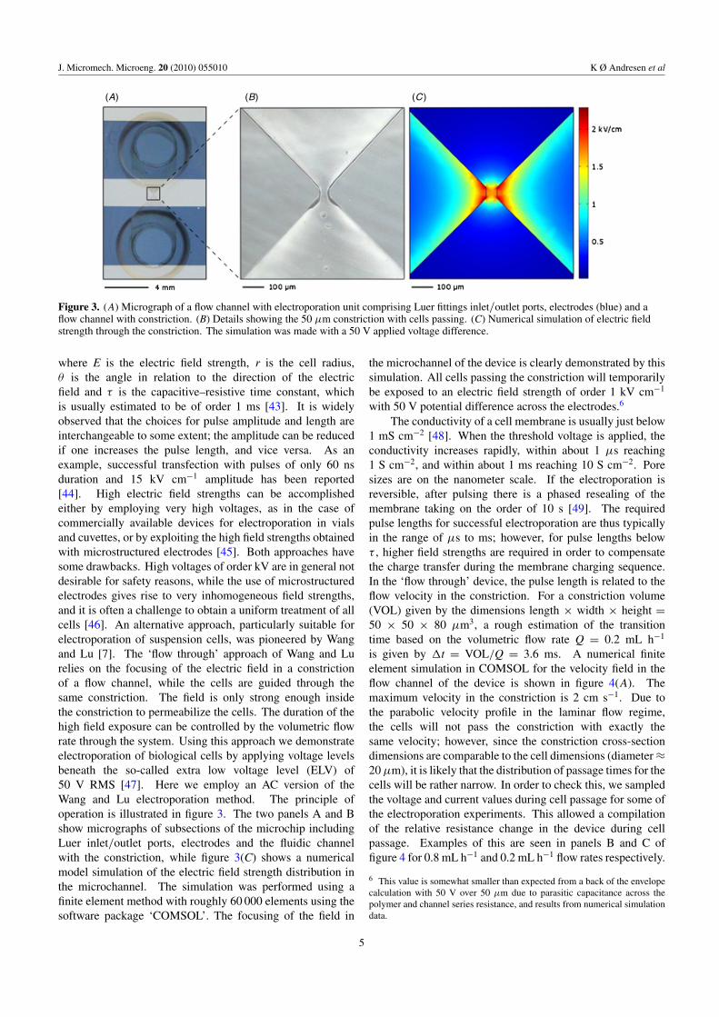
(A) (B) (C )
Figure 3. (A) Micrograph of a flow channel with electroporation unit comprising Luer fittings inlet/outlet ports, electrodes (blue) and aflow channel with constriction. (B) Details showing the 50 μm constriction with cells passing. (C) Numerical simulation of electric fieldstrength through the constriction. The simulation was made with a 50 V applied voltage difference.
where E is the electric field strength, r is the cell radius,θ is the angle in relation to the direction of the electricfield and τ is the capacitive–resistive time constant, whichis usually estimated to be of order 1 ms [43]. It is widelyobserved that the choices for pulse amplitude and length areinterchangeable to some extent; the amplitude can be reducedif one increases the pulse length, and vice versa. As anexample, successful transfection with pulses of only 60 nsduration and 15 kV cm−1 amplitude has been reported[44]. High electric field strengths can be accomplishedeither by employing very high voltages, as in the case ofcommercially available devices for electroporation in vialsand cuvettes, or by exploiting the high field strengths obtainedwith microstructured electrodes [45]. Both approaches havesome drawbacks. High voltages of order kV are in general notdesirable for safety reasons, while the use of microstructuredelectrodes gives rise to very inhomogeneous field strengths,and it is often a challenge to obtain a uniform treatment of allcells [46]. An alternative approach, particularly suitable forelectroporation of suspension cells, was pioneered by Wangand Lu [7]. The ‘flow through’ approach of Wang and Lurelies on the focusing of the electric field in a constrictionof a flow channel, while the cells are guided through thesame constriction. The field is only strong enough insidethe constriction to permeabilize the cells. The duration of thehigh field exposure can be controlled by the volumetric flowrate through the system. Using this approach we demonstrateelectroporation of biological cells by applying voltage levelsbeneath the so-called extra low voltage level (ELV) of50 V RMS [47]. Here we employ an AC version of theWang and Lu electroporation method. The principle ofoperation is illustrated in figure 3. The two panels A and Bshow micrographs of subsections of the microchip includingLuer inlet/outlet ports, electrodes and the fluidic channelwith the constriction, while figure 3(C) shows a numericalmodel simulation of the electric field strength distribution inthe microchannel. The simulation was performed using afinite element method with roughly 60 000 elements using thesoftware package ‘COMSOL’. The focusing of the field in
the microchannel of the device is clearly demonstrated by thissimulation. All cells passing the constriction will temporarilybe exposed to an electric field strength of order 1 kV cm−1
with 50 V potential difference across the electrodes.6
The conductivity of a cell membrane is usually just below1 mS cm−2 [48]. When the threshold voltage is applied, theconductivity increases rapidly, within about 1 μs reaching1 S cm−2, and within about 1 ms reaching 10 S cm−2. Poresizes are on the nanometer scale. If the electroporation isreversible, after pulsing there is a phased resealing of themembrane taking on the order of 10 s [49]. The requiredpulse lengths for successful electroporation are thus typicallyin the range of μs to ms; however, for pulse lengths belowτ , higher field strengths are required in order to compensatethe charge transfer during the membrane charging sequence.In the ‘flow through’ device, the pulse length is related to theflow velocity in the constriction. For a constriction volume(VOL) given by the dimensions length × width × height =50 × 50 × 80 μm3, a rough estimation of the transitiontime based on the volumetric flow rate Q = 0.2 mL h−1
is given by �t = VOL/Q = 3.6 ms. A numerical finiteelement simulation in COMSOL for the velocity field in theflow channel of the device is shown in figure 4(A). Themaximum velocity in the constriction is 2 cm s−1. Due tothe parabolic velocity profile in the laminar flow regime,the cells will not pass the constriction with exactly thesame velocity; however, since the constriction cross-sectiondimensions are comparable to the cell dimensions (diameter ≈20 μm), it is likely that the distribution of passage times for thecells will be rather narrow. In order to check this, we sampledthe voltage and current values during cell passage for some ofthe electroporation experiments. This allowed a compilationof the relative resistance change in the device during cellpassage. Examples of this are seen in panels B and C offigure 4 for 0.8 mL h−1 and 0.2 mL h−1 flow rates respectively.
6 This value is somewhat smaller than expected from a back of the envelopecalculation with 50 V over 50 μm due to parasitic capacitance across thepolymer and channel series resistance, and results from numerical simulationdata.
5

J. Micromech. Microeng. 20 (2010) 055010 K Ø Andresen et al
(A)
(B)
(C)
Figure 4. (A) Numerical simulation of the velocity field through theconstriction. (B) Relative resistance change of the microfluidicchannel as a function of time recorded as a cell passes theconstriction (black data points). The volumetric flow rate was0.8 mL h−1. The full red curve is a Gaussian function fitted to thedata with FWHM 1.2 ms. (C) Same as B but with 0.2 mL h−1 flowrate and Gaussian function with FWHM = 4.3 ms.
The data can be understood qualitatively by assuming that cellsdisplace conducting buffer from the constriction when theypass. Hence, a transient rise in the resistance will result when
a cell passes the constriction, in much the same way as in aCoulter particle counter [50]. The resistance of the constrictionis about 1/3 of the overall resistance of the device, and anestimate of the transient amplitude for passage of a cell is givenby the ratio of cell volume and constriction volume �R/R =(1/3) · Volcell/Volconstr., which for the signal amplitudes infigure 4 corresponds to realistic cell radii of approximately8 μm. In order to evaluate the transit times, we observedthat the measured resistance peaks empirically could be fittedto Gaussian functions, allowing an estimation of the transittimes from the resulting full width half maximum (FWHM)of the Gaussians. The data did not allow a determinationof the distribution of transit times, but gave a fairly goodestimate of typical transit times. The transit times scaledwell with the flow rate through the device. Hence, the transittime for cells passing with a flow rate of 0.8 mL h−1 wasroughly four times shorter than for 0.2 mL h−1 flow rateas expected. Considering these measurements the questionthat naturally arises is whether cells that were permeabilizedcould be distinguished from nonpermeabilized cells due tothe imposed difference in membrane conductance of the twospecies. This was, however, not possible with the present data,probably because the induced membrane conductance changewas too small.
The next consideration relates to the frequency ofoperation for application of the electric field. Clearly, even50 V is a very high voltage, and electrode reactions wouldreadily cause serious deterioration of the PEDOT electrodesif operated in DC mode. However, here one can rely onthe massive capacitances usually formed between electrodesand electrolytes due to the very thin Helmholtz double layers[51]. The large capacitances ensure a capacitive coupling tothe electrolyte at even moderate frequencies. To this end, wecharacterized the devices by impedance spectroscopy with astandard PBS buffer as the electrolyte and a solution dilutedwith sugar. This was done using a potentiostat (from PrincetonApplied Research, model: Versastat 3). The results for thePBS buffer are shown in figure 5(A), where the magnitude andphase of the impedance is plotted as a function of frequency.The layout of the device comprising electrodes and channelis shown in (B). A lumped element model, shown in (C),was constructed to fit the impedance spectroscopy data. Themodel comprised electrode resistors Re, interface resistorsRi , interface capacitors Ci , channel resistor Rc and channelcapacitor Cc. Re was obtained independently, simply bymeasuring the electrode resistance without PBS buffer with anohmmeter between the relevant ports for electrical connectionand fluid access (see figure 5). Re amounted to roughly 2 k�.Ri (3 k�) represents the undesirable connection betweenelectrode and buffer involving electrode redox reactions, whileCi represents the huge electrode capacitance of 20 μF. Rc isthe channel resistance fitted to 35 k�, while Cc is a small(10 pF) parasitic channel capacitance originating from electricfield lines spreading into the polymer wall material around theconstriction, as can be observed in the numerical simulationin the figure. Cc is responsible for the high frequency(>10 kHz) low pass filter behavior observed as a decay ofimpedance magnitude at high frequencies. The huge interface
6

J. Micromech. Microeng. 20 (2010) 055010 K Ø Andresen et al
(A)
(B) (C)
Figure 5. (A) Magnitude (•) and phase (�) of complex impedancerecorded as a function of frequency. Full red and blue curves are fitsto a lumped element model. (B) Layout of channel sectionconstituting the model. The light green feature is the channel layout,while the dark green feature is the electrode layout. (C) The lumpedelement model constructed to make the fit in (A). The modelcomprised electrode resistors Re (2 k�), interface resistors Ri
(3 k�), interface capacitors Ci (20 μF), channel resistor Rc (35 k�)and channel capacitor Cc (10 pF).
capacitance is caused by the very thin Helmholtz double layerof the order of the Debye length LD =
√εkBT /2e2c ≈
1 nm. Here ε is the dielectric constant of water, kB
is Boltzmann’s constant, T is the absolute temperature, eis the elementary charge, and c is the ion concentration.For fitting the impedance data, Ci was replaced by a so-called constant phase element (CPE) with complex admittanceYCPE = (iω/2π · Hz)α2π · Hz · Ci .7 In the fitting α = 0.9 wasused. The CPE concept is usually ascribed to the roughnessof electrodes [52]. For α = 1, CPE reduces to the normaladmittance for a capacitor. As can be seen in figure 5, thelumped element model breaks down at frequencies belowapproximately 7 Hz, where the electrode reactions dominate,and this phenomenon cannot simply be represented by aresistor model. Also it can easily be seen that Ri becomesentirely shunted approximately at 1 kHz by the current runningthrough Ci . For even higher frequencies, the parasitic channelcapacitor begins to play a role, and shunts the electric fieldin the constriction. The behavior was qualitatively similar forthe diluted buffer; only the fitted values for the channel and
7 The non-elegant inclusion of the Hz frequency unit in the CPE formula isrequired for using the formula with SI units.
interface resistances changed. Consequently it was chosen tooperate the devices at 1 kHz, square ±50 V pulses, althoughsome decrease in field strength across the cell membranes wasexpected at the cross-over from positive to negative potentialdue to the charging of cell membranes, which are expected tocharge with a capacitive–resistive time constant [43] of order1 ms.8
For the electroporation experiments, a diluted buffersolution was used. This was done to decrease the bufferconductivity to avoid formation of gas bubbles in theconstriction due to electrolysis of water molecules. The PBSbuffer solution is widely used in biological research, is isotonicand serves to help maintain a constant pH of about 7.4, buthas a rather high conductivity of 1.7 S m−1 at 300 K. Thecomposition is 138 mM NaCl, 10 mM phosphate and 2.7 mMKCl. For our purpose, the NaCl concentration was reducedto 20 mM by the following procedure: for 100 mL of finalsolution, 14.6 mL PBS buffer was mixed with 4.6 g of glucose(C6H6O6), and water was added until the solution reached100 mL. This reduced the conductivity of the buffer by roughlya factor of 6.5 while maintaining the osmolarity.
Successful electroporation experiments on THP-1 cellswere performed at 30 V and 50 V applied voltage, using aflow rate of 0.2 mL h−1 corresponding to an exposure time of3.6 ms. For a 50 V applied voltage, the numerical simulationspredict an electric field peak strength of order 1.7 kV cm−1 anda potential difference across the cell of order 2 V according toequation (1) and assuming cell radii of order 8 μm. The resultsof the electroporation experiments are seen in figure 6 for 30 Vand 50 V square pulses respectively. For 50 V pulses SYTOXGreen fluorescent dye was delivered to 46 ± 3% of the cells,while for 30 V pulses the dye was delivered to 14 ± 3% of thecells. The uncertainties for successful dye delivery fractionswere obtained by averaging over several microscope images.The control experiments, where the cells were subjected tothe same treatment except for application of the electric fields,showed delivery levels of order 8 ± 3% in both the 50 Vand the 30 V experiments. A higher delivery fraction couldlikely be obtained by slightly higher voltage levels. However,this caused runaway heating phenomena in the constrictioneven with the sugar substituted buffer solution and would notallow compliance with the ELV standard [47]. In order toincrease the delivery rate, the constriction could easily beredesigned to become shallower, less wide or comprisingparallel constrictions. The only negative effect of this designchange would be the requirement to decrease the flow rate inorder not to decrease the exposure time to the field. Such adesign change would cause more sedimentation of cells, but anatural counter measure would be to increase the length of thechannel accordingly.
In the present work, we focus on demonstratingpermeation of the cell membrane on real biological cells inour all-polymer device rather than assuring a high viability ofcells after electroporation. The SYTOX Green dye will staincells with a compromised cell membrane, hence, both dead andtransfected cells. For a study with focus on real applications
8 Assuming a membrane capacitance CM ≈ 1μFcm2 and a membrane resistance
RM ≈ 1 k� cm2.
7

J. Micromech. Microeng. 20 (2010) 055010 K Ø Andresen et al
Figure 6. Histogram showing fractions of fluorescent cells afterelectroporation with ±30 V and ±50 V square pulses at 1 kHz. Thecontrol fractions refer to the data taken with cells from the sameculture exposed to exactly the same treatment as the electroporatedones, except for the exposure to the electric field.
of the method, systematic experiments would be needed todocument cell viability after electroporation, by e.g. applyinga second vital stain such as Trypan blue. However, we didperform time-lapse microscopy for some of the electroporatedcells, and found a significant part of the transfected cells viable,but a systematic study providing statistics was consideredoutside the scope of this work and was not carried out.
4. Conclusion
An all polymer single use electroporation chip was fabricatedby means of a rapid prototyping method comprisingmicroinjection molding9. Several hundred parts werefabricated by lithographic definition of father electroforms andsubsequent replication by injection molding. Injection moldedparts were further processed to integrate conducting polymer(PEDOT) electrodes and assembled by thermal bonding. Thefeasibility of having a fixed macroscopic basic form withLuer fitting input/output ports for both fluidic and electricalaccess combined with a flexible rapid prototyping fluidicchannel layout system was demonstrated. The devices werecharacterized by numerical simulations and experiments toidentify the parameter space for successful operation, inparticular the parameters relating to voltage and frequencyranges of applied voltage pulses, and to the fluidic properties.In particular it was demonstrated that thin film PEDOTelectrodes could withstand application of high voltages ifoperated at frequencies where the electrode redox reactionsare shunted by capacitive coupling to the electrolyte. ‘Flowthrough’ electroporation with feasible exposure times wasdemonstrated in experiments carried out on human acute
9 Microinjection molding in this context refer to injection molding usingmicrostructured mold inserts, and not injection molding using a so-calledmicro injection molding machine.
monocytic leukemia THP-1 cells. Delivery fractions ofroughly half of the cell population were demonstrated bydelivering a polynucleotide dye into the cells.
Acknowledgments
We would like to thank Dr Gertrud M Hjortø, DTU-Nanotech,for assistance with the cell handling, and Dr Eugen Stamate,RISØ-DTU, for assistance with the amplifier set-up.
References
[1] Fox M B, Esveld D C, Valero A, Luttge R, Mastwijk H C,Bartels P V, Van Den Berg A and Boom R M 2006 Anal.Bioanal. Chem. 385 474–85
[2] Huang Y and Rubinsky B 2003 Sensors Actuators A104 205–12
[3] Tjelle T E, Corthay A, Lunde E, Sandlie I, Michaelsen T E,Mathiesen I and Bogen B 2004 Mol. Ther. 9 328–36
[4] Shizuya H, Birren B, Kim U-J, Mancino V, Slepak T,Tachiiri Y and Simon M 1992 Proc. Natl Acad. Sci. USA89 8794–7
[5] Tsong T Y 1991 Biophys. J. 60 297–306[6] Huang Y and Rubinsky B 2001 Sensors Actuators A 89 242–9[7] Wang H-Y and Lu C 2006 Anal. Chem. 78 5158–64
Wang H-Y and Lu C 2008 Biotech. Bioeng. 100 579[8] International Standard ISO 594-1 1st edn 1986[9] Wu Z, Xanthopoulos N, Reymond F, Rossier J S and
Girault H H 2002 Electrophoresis 23 782–90[10] Becker H and Locascio L E 2002 Talanta 56 267–87[11] Duffy D C, Cooper McDonald J, Schueller O J A
and Whitesides G M 1998 Anal. Chem. 70 4974–84[12] Klank H, Kutter J P and Geschke O 2002 Lab Chip 2 242–6[13] Harrison D J, Fluri K, Seiler K, Fan Z, Effenhauser C S
and Manz A 1993 Science 261 895–7[14] Andersson H and Van Den Berg A 2003 Sensors Actuators B
92 315–25[15] de Mello A 2002 Lab Chip 2 31N–6N[16] Figeys D and Pinto D 2000 Anal. Chem. 72 330A[17] Curtis A and Wilkinson C 2001 Trends Biotechnol. 19 97[18] Clayton J 2005 Nat. Methods 2 621[19] Spegel C, Heiskanen A, Pedersen S, Emneus J, Ruzgasd T
and Taboryski R 2008 Lab Chip 8 323–9[20] Asmild M et al 2003 Receptors Channels 9 49–58[21] Sigworth F J and Klemic K G 2005 IEEE Trans. Nanobiosci.
4 121[22] Heckele M and Schomburg W K 2004 J. Micromech.
Microeng. 14 R1–R14[23] Giboz J, Copponnex T and Mele P 2007 J. Micromech.
Microeng 17 R96–R109[24] Becker H and Gartner C 2008 Anal. Bioanal. Chem.
390 89–111[25] Ekstrand G, Holmquist C, Orlefors A E, Hellman B, Larson A
and Andersson P 2000 Micro Total Analysis Systems 2000ed A van den Berg, W Olthius and P Bergveld (Dordrecht:Kluwer) pp 249–52
[26] Dang F, Tabata O, Kurokawa M, Ewis A A, Zhang L,Yamaoka Y, Shinohara S, Shinohara Y, Ishikawa Mand Baba Y 2005 Anal. Chem. 77 2140–6
[27] Romankiv L T 1997 Electrochem. Acta 42 2985–3005[28] Becker E W, Ehrfeld W, Miinchmeyer D, Betz H,
Heuberger A, Pongratz S, Glashauser W, Michel H Jand Siemens R v 1982 Naturwissenschaften 69 520–3
[29] Piotter V, Hanemann T, Ruprecht R and Haußelt J 1997Microsyst. Technol. 3 129–33
8
J. Micromech. Microeng. 20 (2010) 055010 K Ø Andresen et al
[30] Monkkonen K, Hietala J, Paakonen P, Paakonen E J,Kaikuranta T, Pakkanen T T and Jaaskelainen T 2002Pol. Eng. Sci. 42 1600
[31] Pranov H, Koblitz Rasmussen H, Larsen N B andGadegaard N 2006 Pol. Eng. Sci. 46 160–71
[32] McCormick R M, Nelson R J, AlonsoAmigo M G, Benvegnu Jand Hooper H H 1997 Anal. Chem. 69 2626–30
[33] Gadegaard N, Mosler S and Larsen N B 2003 Macromol.Mater. Eng. 288 76–83
[34] Mair D A, Geiger E, Pisano A P, Frechet J M J and Svec F2006 Lab Chip 6 1346–54
[35] Chien R-D 2006 Sensors Actuators A 128 238–47[36] Zou Z, Lee S and Ahn C H 2008 IEEE Sens. J. 8 527[37] Hansen T S, West K, Hassager O and Larsen N B 2007
J. Micromech. Microeng. 17 860–6[38] Tsao C-W and DeVoe D L 2009 Microfluid Nanofluid
6 1–16[39] Hyun J, Aspnes D E and Cuomo J J 2001 Macromolecules
34 2395–7[40] Martinet W, Schrijvers D M and Kockx M M 2003 Biotech.
Lett. 25 1025–9
[41] Coster H G L and Zimmermann U 1975 J. Membr. Biol.22 73–90
[42] Lundqvist J A, Sahlin F, Aberg M A I, Stromberg A,Eriksson P S and Orwar O 1998 Proc. Natl Acad. Sci.95 10356–60
[43] Malmivuo J and Plonsey R 1995 Bioelectromagnetism (NewYork: Oxford University Press) chapter 3
[44] White J A, Blackmore P F, Schoenbach K H andBeebe Stephen J 2004 J. Biol. Chem. 279 22964–72
[45] Sedgwick H, Caron F, Monaghan P B, Kolch W andCooper J M 2008 J.R. Soc. Interface 5 123-S130
[46] MacQueen L A, Buschmann M D and Wertheimer M R 2008Bioelectrochemistry 72 141–8
[47] International Electrotechnical Commission standard: IEC60364-4-41 Ed. 5.0 b:2005
[48] Jeuken L J C 2008 Biophys. J. 94 4711–7[49] Pucihar G, Kotnik T, Miklavc D and Teissie J 2008 Biophys. J.
95 2837–48[50] Gawad S, Schild L and Renaud Ph 2001 Lab Chip 1 76–82[51] Kotz R and Carlen M 2000 Electrochim. Acta 45 2483–98[52] Pajkossy T 1994 J. Electroanal. Chem. 364 111–25
9