Hydromagnetic nonlinear thermally radiative nanoliquid flow ...

lable at ScienceDirect
Journal of Alloys and Compounds 648 (2015) 280e290
Contents lists avai
Journal of Alloys and Compounds
journal homepage: http: / /www.elsevier .com/locate/ ja lcom
Influence of composition on optical and dispersion parameters ofthermally evaporated non-crystalline Cd50S50�xSex thin films
A.S. Hassanien a, b, *, 1, Alaa A. Akl b
a Engineering Mathematics and Physics Dept., Faculty of Engineering (Shoubra), Benha University, Egyptb Physics Department, Faculty of Science and Humanities in Ad-Dawadmi, Shaqra University, 11911, Saudi Arabia
a r t i c l e i n f o
Article history:Received 26 February 2015Received in revised form13 June 2015Accepted 26 June 2015Available online 2 July 2015
Keywords:Amorphous materialsChalcogenidesThin filmsPhysical vapor deposition (PVD)Optical properties
* Corresponding author. Engineering MathematicsEngineering (Shoubra), Benha University, Egypt.
E-mail address: [email protected] (A.S. Ha1 On leave to: Physics Department, Faculty of Sci
Dawadmi, Shaqra University, 11911, Saudi Arabia.
http://dx.doi.org/10.1016/j.jallcom.2015.06.2310925-8388/© 2015 Elsevier B.V. All rights reserved.
a b s t r a c t
Non-crystalline thin films of chalcogenide Cd50S50�xSex system (30 � x � 50) were obtained by thermalevaporation technique onto a pre-cleaned glass substrate at a vacuum of 8.2 � 10�4 Pa. The depositionrate and film thickness were kept constant at about 8 nm/s and 200 nm, respectively. Amorphous/crystalline nature and chemical composition of films have been checked using X-ray diffraction andenergy dispersive X-ray spectroscopy (EDX). Optical properties of thin films were investigated andstudied using the corrected transmittance, T(l) and corrected reflectance, R(l) measurements. Obtaineddata reveal that, the indirect optical energy gap (Eg) was decreased from 2.21 to 1.57 eV. On the contrary,Urbach energy (band tail width), EU was found to be increased from 0.29 to 0.45 eV. This behavior isbelieved to be associated with the increase of Se-content instead of S-content in the thin films ofCd50S50�xSex system. Chemical bond approach model, CBA was used to analyze the obtained values of Egand EU. Optical density, skin depth, extinction coefficient, refractive index and optical conductivity ofchalcogenide CdSSe thin films were discussed as functions of Se-content. Using Wemple-DiDomenicosingle oscillator model, the refractive index dispersion and energy parameters and their dependenceon Se content were studied.
© 2015 Elsevier B.V. All rights reserved.
1. Introduction
Recently, IIeVI semiconducting materials including the chalco-genide compounds and alloys are extremely vibrant because oftheir interesting properties; e.g. wide band gap, high absorptioncoefficients, binding energy, high chemical stability, andenvironment-friendly applications [1,2]. Chalcogenide alloy is asolid solution composition containing one or more chalcogenideelement of the group 16 in the periodic table. They includeelemental chalcogens, pure or doped S, Se and Te, and their alloys[3]. Chalcogenide alloy also, forms a large group of non-crystallineamorphous compounds. Recently, these amorphous alloys havebeen given great attention due to the fact that: (i) they are relativelyeasy to prepare in large sizes (ii) their wide range of applications inseveral technological and scientific fields [4]. Ternary chalcogenide
and Physics Dept., Faculty of
ssanien).ence and Humanities in Ad-
CdSSe systems are considered to be promising compounds becauseof their several modern potential technological applications. So,they have received considerable attention of many researchers [5].CdSSe compositions are used widely in many applications likeoptical filters, holography, optical waveguides, temperature sensor[6e8], gas sensors, environmental sensors, piezoelectric devices,optical switching, light emitting diodes, infrared photo-detectors,electron-beam pumped lasers [9e13], spintronics, quantumcomputing, electro-photography, photo-electrochemical, photo-catalysis, opto-electronic devices and solar cells [13,14]. Chalco-genide CdSSe thin films are also characterized by their high sensi-tivity to light, therefore, they are used along wide ranges ofapplication, especially in transistors and electroluminescent de-vices [15,16]. As a result of the importance of ternary CdSSe com-pounds and their multiple uses, we find these compounds occupy alarge scientific research area [9e16]. CdSSe can be easily preparedeither in amorphous glassy or crystalline form. Getting samples ofamorphous or crystalline nature depends on the conditions ofpreparation and growing process. However, the difficult task is tosynthesis multi-component chalcogenide thin films with high ho-mogeneity from their ingredients and at the same time have

A.S. Hassanien, A.A. Akl / Journal of Alloys and Compounds 648 (2015) 280e290 281
homogenous thicknesses. Ternary thin films of CdSSe network havebeen prepared using various techniques, e.g. chemical bath depo-sition, CBD [17,18], spray pyrolysis technique, SPT [19], pulse platingtechnique, PPT [20], screen-printing followed by sintering [21] andlaser ablation technique [22]. In addition to all thesemethods, thereis the thermal evaporation technique, which is considered to be themost accurate one, where all preparative conditions (evaporationrate, film thickness, surface morphology and the structural state)can be controlled, therefore it produces high quality thin films[23e26]. This technique has been already used to synthesis theternary compounds of CdSSe thin films [24]. On the other hand, X-ray diffraction is considered a suitable method for checking thecrystalline/amorphous nature of thin films, especially if the scan-ning rate is a continuous and slow. Moreover X-ray diffractogramsgive good and sufficient information about the nature of formingthin films rather than it is a low cost, fast, easy method and a veryreliable technique [27e29]. This communication is a continuationof previous research works where authors studied nanostructure,optical and electrical properties of thermally evaporated CdS0.1Se0.9polycrystalline thin films with different thickness in one article [24]and in another work they studied the microstructure and crystal-line imperfections of the ternary chalcogenide systems ofCdSXSe1�X thin films with compositions where 0.0 � x � 0.4 [27].The motivation of our present work is to fabricate high homoge-neity non-crystalline thin films of Cd50S50�xSex using the thermalevaporation process and to investigate, study and connect the op-tical properties, optical parameters and the dispersion of therefractive index as well as studying the dispersion energy param-eters of these evaporated thin films with the Se content. Our aim isalso to determine the optical energy gap, Eg and the band tail width,EU and interpret their values in view of the chemical bond approachmodel, CBA. Another aim is also to correlate Eg and EU values to thevalues of both the cohesive energy and the average coordinationnumber of the amorphous Cd50S50�xSex system under investigation[30,31].
2. Experimental work
High purity Cd, S and Se powdered materials (Sigma-Aldrich)were weighted in appropriate proportions according to theiratomic mass ratios in stoichiometric quantities. An electronicbalance (5-digits) was used to get the desired amount of CdSSecompositions. The inputs starting materials were mixed very wellto synthesis the ternary chalcogenide thin films of Cd50S50�xSex(x ¼ 30, 35, 40, 45, and 50%). Cadmium sulphoselenide networkwere prepared by the solid-state method. The starting materialswere extremely grinded together using a tightly closed agatemortar. The grinded mixture was placed in a roll mill for 48 h toget a highly homogeneous mixture. The homogenous mixture ofCd, S and Se were pressed together using high pressurecompressor (6.5 MPa), to get highly compressed solid pellets.These pellets were used to get the thin films by the thermalevaporation process. These pellets were placed in the molybde-num boat source of the coating unit. Thus, fragmentation orscattering of the components of Cd50S50�xSex matrix can beavoided. Thin films were deposited on pre-cleaned glass sub-strates. The substrates were thoroughly cleaned several timesusing a detergent solution, a mixture of hydrochloric and nitricacids, ethanol and acetone, rinsed in distilled water and finallyultrasonically carefully cleaned. The evaporation process wascarried out by Edward's coating unit (E 306A) maintaining theresidual vacuum in the order of 8.2 � 10�4 Pa. The rate of depo-sition process was kept constant for all films at 8 nm/s approxi-mately. Film thickness and deposition rate were monitored duringthe deposition process by a quartz crystal oscillator (Edwards
model FTM3). The quartz oscillator is located very close to thesubstrate inside the chamber of the thermal evaporation. Filmthicknesses were checked by multiple-beam Fizeau fringes atreflection method. CdSSe thin films were controlled in to havethickness of 200 ± 3 nm. Thin films were kept inside the deposi-tion chamber for 24 h to achieve the meta stable equilibrium state.The obtained as-deposited thin films were uniform, smooth andtightly adherent to the glass substrates. The colors of the depos-ited thin films have changed gradually from yellow to yellowishorange and finally they became have dark orange red color byadding of more Se to the ternary system of Cd50S50�xSex(30 � x �50). The change in film colors by increasing of Se-contentindicates the substitution of S2� by Se2� ions in the preparedternary CdSSe thin films. The amorphous/Crystalline nature offilms was checked by JEOL X-ray diffractometer (Model JSDX-60PA) that was operated at 40 kV and 35 mA. The used sourcewas Cu-ka-radiation, which has the wavelength 0.154184 nm andenergy 8.042 keV. This powerful energy is sufficient to wellexamine the deposited thin films. Continuous scanning wasapplied with a slow scanning rate (1�/min) and a small timeconstant (1 s) to detect any probable diffraction line. X-raydiffraction traces of all samples were taken at room temperature.The diffraction angle (2q) of XRD patterns was ranged from 4� to100�. The elemental composition of our chalcogenideCd50S50�xSex thin films was investigated using energy dispersiveanalysis of X-rays (EDAX) interfaced with a scanning electronmicroscope operating with an accelerating voltage of 30 kV. Therelative error in determining the indicated elements does notexceed ±0.2%. Transmission, T(l) and reflection, R(l) spectra wereobtained using a Shimadzu UV310PC; UVevISeNIR double beamspectrophotometer with a reflection attachment of VeN type. R(l)measurements were carried out at the incident angle 5� from thenormal to the sample surface. Optical properties of CdSSe non-crystalline thin films of CdSSe matrix were studied from the cor-rected transmittance, T(l) and the corrected reflectance, R(l), inthe range 300e2500 nm. All optical investigations were achievedat room temperature (300 K) Some published and calculatedvalues which concern the starting materials (Cd, S and Se) andtheir binary compounds were reported in Tables 1 and 2 [32,33].
3. Results and discussion
3.1. X-ray diffraction characterization
Thin films of the chalcogenide Cd50S50�xSex systems(30 � x � 50) were characterized by X-ray diffraction. Fig. 1 revealsthat, for all thin films of Cd50S50�xSex network, no discrete or sharpdiffraction lines were observed. This confirms the amorphous na-ture of as deposited thin films regardless of selenium content. TheX-ray diffraction traces of all thin films were measured at roomtemperature and found to show almost similar trends. Thecompositional distribution of the constituent elements of theevaporated thin films of the amorphous ternary systems ofCd50S50�xSex (30 � x � 50) with thickness 200 nmwas reported inTable 3. It was found that the measured and the calculated values ofthe prepared thin films for all CdSSe compositions are very close toeach other, where the error does not exceed ±0.2%.
3.2. Optical properties studies
Optical properties study of the chalcogenide thin films ofCd50S50�xSex matrix plays an important role in understanding theoptoelectronic nature [13,14]. These properties can be interpretedin the view of the interaction between the incident photons and thesemiconducting films. Furthermore, optical properties of thin films
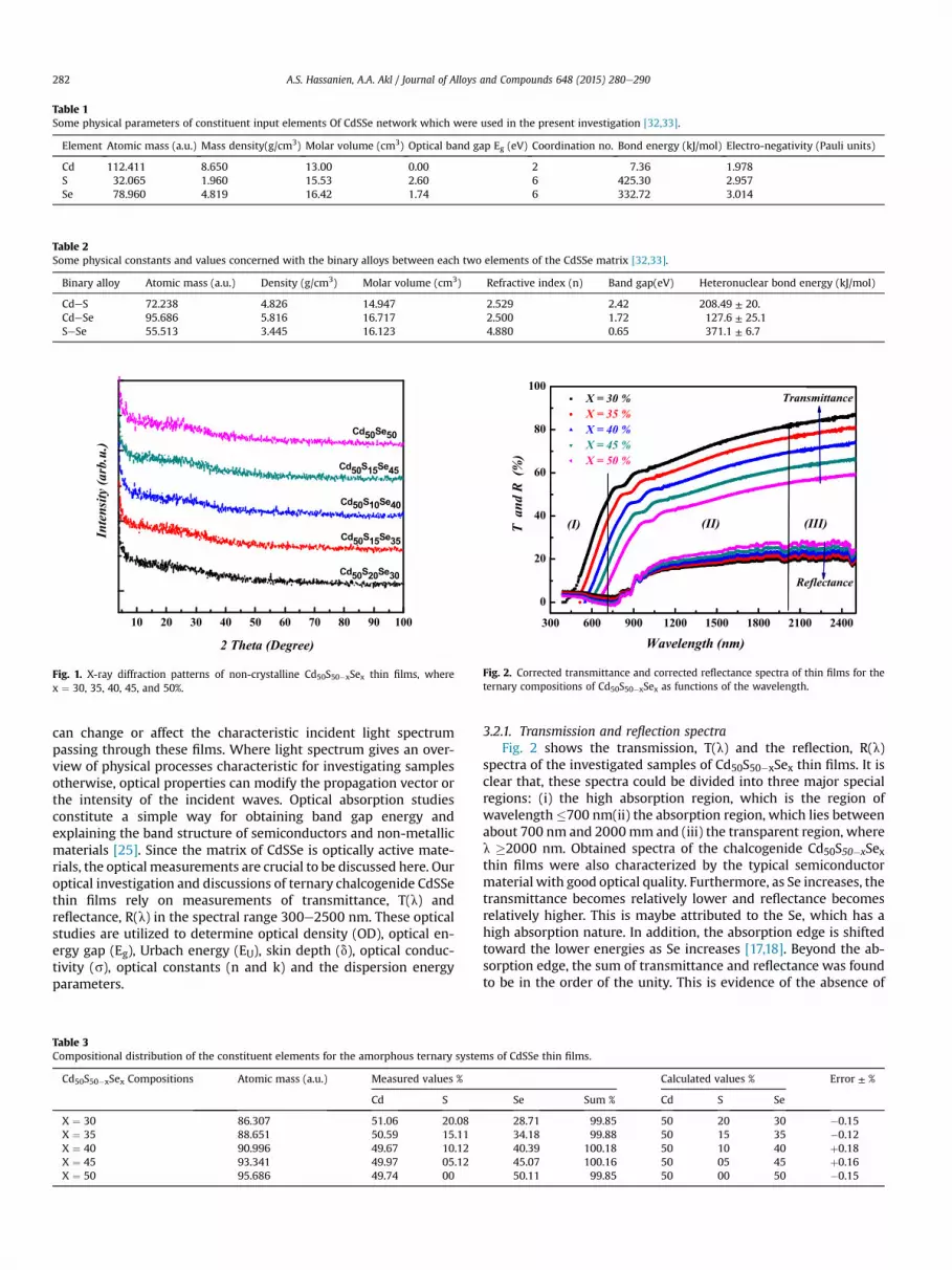
Table 1Some physical parameters of constituent input elements Of CdSSe network which were used in the present investigation [32,33].
Element Atomic mass (a.u.) Mass density(g/cm3) Molar volume (cm3) Optical band gap Eg (eV) Coordination no. Bond energy (kJ/mol) Electro-negativity (Pauli units)
Cd 112.411 8.650 13.00 0.00 2 7.36 1.978S 32.065 1.960 15.53 2.60 6 425.30 2.957Se 78.960 4.819 16.42 1.74 6 332.72 3.014
Table 2Some physical constants and values concerned with the binary alloys between each two elements of the CdSSe matrix [32,33].
Binary alloy Atomic mass (a.u.) Density (g/cm3) Molar volume (cm3) Refractive index (n) Band gap(eV) Heteronuclear bond energy (kJ/mol)
CdeS 72.238 4.826 14.947 2.529 2.42 208.49 ± 20.CdeSe 95.686 5.816 16.717 2.500 1.72 127.6 ± 25.1SeSe 55.513 3.445 16.123 4.880 0.65 371.1 ± 6.7
10 20 30 40 50 60 70 80 90 100
Cd50S20Se30
Cd50S15Se35
Cd50Se50
2 Theta (Degree)
Cd50S10Se40
Inte
nsity
(arb
.u.)
Cd50S15Se45
Fig. 1. X-ray diffraction patterns of non-crystalline Cd50S50�xSex thin films, wherex ¼ 30, 35, 40, 45, and 50%.
300 600 900 1200 1500 1800 2100 2400
0
20
40
60
80
100
T a
nd R
(%
)
Wavelength (nm)
Reflectance
Transmittance X = 30 % X = 35 %X = 40 %X = 45 %X = 50 %
(I) (II) (III)
Fig. 2. Corrected transmittance and corrected reflectance spectra of thin films for theternary compositions of Cd50S50�xSex as functions of the wavelength.
A.S. Hassanien, A.A. Akl / Journal of Alloys and Compounds 648 (2015) 280e290282
can change or affect the characteristic incident light spectrumpassing through these films. Where light spectrum gives an over-view of physical processes characteristic for investigating samplesotherwise, optical properties can modify the propagation vector orthe intensity of the incident waves. Optical absorption studiesconstitute a simple way for obtaining band gap energy andexplaining the band structure of semiconductors and non-metallicmaterials [25]. Since the matrix of CdSSe is optically active mate-rials, the optical measurements are crucial to be discussed here. Ouroptical investigation and discussions of ternary chalcogenide CdSSethin films rely on measurements of transmittance, T(l) andreflectance, R(l) in the spectral range 300e2500 nm. These opticalstudies are utilized to determine optical density (OD), optical en-ergy gap (Eg), Urbach energy (EU), skin depth (d), optical conduc-tivity (s), optical constants (n and k) and the dispersion energyparameters.
Table 3Compositional distribution of the constituent elements for the amorphous ternary syste
Cd50S50�xSex Compositions Atomic mass (a.u.) Measured values %
Cd S
X ¼ 30 86.307 51.06 20.08X ¼ 35 88.651 50.59 15.11X ¼ 40 90.996 49.67 10.12X ¼ 45 93.341 49.97 05.12X ¼ 50 95.686 49.74 00
3.2.1. Transmission and reflection spectraFig. 2 shows the transmission, T(l) and the reflection, R(l)
spectra of the investigated samples of Cd50S50�xSex thin films. It isclear that, these spectra could be divided into three major specialregions: (i) the high absorption region, which is the region ofwavelength�700 nm(ii) the absorption region, which lies betweenabout 700 nm and 2000mm and (iii) the transparent region, wherel �2000 nm. Obtained spectra of the chalcogenide Cd50S50�xSexthin films were also characterized by the typical semiconductormaterial with good optical quality. Furthermore, as Se increases, thetransmittance becomes relatively lower and reflectance becomesrelatively higher. This is maybe attributed to the Se, which has ahigh absorption nature. In addition, the absorption edge is shiftedtoward the lower energies as Se increases [17,18]. Beyond the ab-sorption edge, the sum of transmittance and reflectance was foundto be in the order of the unity. This is evidence of the absence of
ms of CdSSe thin films.
Calculated values % Error ± %
Se Sum % Cd S Se
28.71 99.85 50 20 30 �0.1534.18 99.88 50 15 35 �0.1240.39 100.18 50 10 40 þ0.1845.07 100.16 50 05 45 þ0.1650.11 99.85 50 00 50 �0.15
300 600 900 1200 1500 1800 2100 24000
400
800
1200
1600
2000
2400A
bsor
ptio
n co
effic
ient
a x
103
(cm
-1 )
Wavelength (nm)
Cd50S20Se30 Cd50S15Se35 Cd50S10Se40 Cd50S5Se45 Cd50Se50
(a)
400 500 600 700 800 9000
300
600
900
1200
Abs
orpt
ion
coef
ficie
nt, (α
X 1
03 (cm
)-1
Wavelenth (nm)
Cd50S20Se30 Cd50S15Se35 Cd50S10Se40 Cd50S5Se45 Cd50Se50
(b)
(
Fig. 3. (a) Optical absorption spectra (b) the shift of absorption edge with increasing ofSe percentage of amorphous Cd50S50�xSex thin films, where x ¼ 30, 35, 40, 45, and 50%.
0.5 1.0 1.5 2.0 2.5 3.00
100
200
300
400
500
Opt
ical
den
sity
, O
D
Photon energy (ev)
Cd50S20Se30 Cd50S15Se35 Cd50S10Se40 Cd50S5Se45 Cd50Se50
Fig. 4. Variation of the optical density, OD as a function of the photon energy for theternary thin films of CdSSe matrix.
0.5 1.0 1.5 2.0 2.5 3.0 3.5
0
500
1000
1500
2000
2500
3000
3500
4000
( αhν
)1/2
(eV/
cm)1/
2
Photon energy, hν (eV)
Cd50S20Se30 Cd50S15Se35 Cd50S10Se40 Cd50S5Se45 Cd50Se50
Fig. 5. Variation of (a hy)1/2 with the photon energy (hy) for the non-crystalline thinfilms of CdSSe matrix.
A.S. Hassanien, A.A. Akl / Journal of Alloys and Compounds 648 (2015) 280e290 283
scattering or absorption of the incident light, which confirms thatthe surfaces of the deposited thin films are of good quality and has asmooth nature [17e19].
3.2.2. Optical absorption studiesAt room temperature, optical absorption spectra of Cd50S50�xSex
thin films have been studied to determine the absorption coeffi-cient, optical energy gap, Eg, band tail width or Urbach energy, EUand the nature of the transitions involved. Knowing the filmthickness (t), the optical absorption coefficient (a) could be deter-mined from the measurements of T(l) and R(l) by using thefollowing equations [34,35]:
Ty�1� R2
�e�at (1)
lnðTÞyln�1� R2
�� at (2)
a ¼ 1tln
�1� R2
�T
(3)
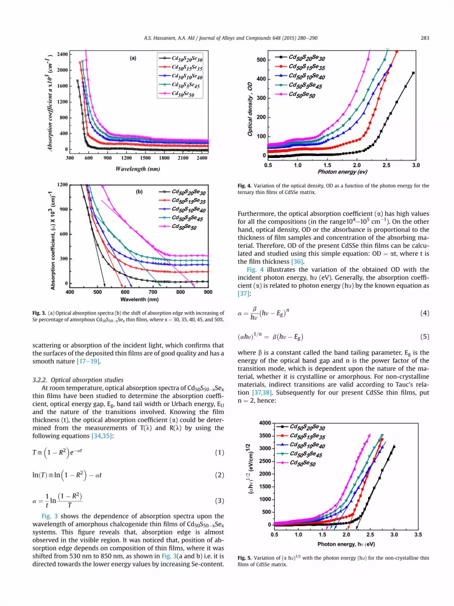
Fig. 3 shows the dependence of absorption spectra upon thewavelength of amorphous chalcogenide thin films of Cd50S50�xSexsystems. This figure reveals that, absorption edge is almostobserved in the visible region. It was noticed that, position of ab-sorption edge depends on composition of thin films, where it wasshifted from 530 nm to 850 nm, as shown in Fig. 3(a and b) i.e. it isdirected towards the lower energy values by increasing Se-content.
Furthermore, the optical absorption coefficient (a) has high valuesfor all the compositions (in the range104e105 cm�1). On the otherhand, optical density, OD or the absorbance is proportional to thethickness of film samples and concentration of the absorbing ma-terial. Therefore, OD of the present CdSSe thin films can be calcu-lated and studied using this simple equation: OD ¼ at, where t isthe film thickness [36].
Fig. 4 illustrates the variation of the obtained OD with theincident photon energy, hy (eV). Generally, the absorption coeffi-cient (a) is related to photon energy (hy) by the known equation as[37]:
a ¼ b
hy
�hy� Eg
�n (4)
ðahyÞ1=n ¼ b�hy� Eg
�(5)
where b is a constant called the band tailing parameter, Eg is theenergy of the optical band gap and n is the power factor of thetransition mode, which is dependent upon the nature of the ma-terial, whether it is crystalline or amorphous. For non-crystallinematerials, indirect transitions are valid according to Tauc's rela-tion [37,38]. Subsequently for our present CdSSe thin films, putn ¼ 2, hence:

A.S. Hassanien, A.A. Akl / Journal of Alloys and Compounds 648 (2015) 280e290284
ðahyÞ1=2 ¼ b�hy� Eg
�(6)
Therefore, plotting ðahyÞ1=2 versus the photon energy (hy), givesa straight line in a certain region. The extrapolation of this straightline will intercept the (hy)-axis to give the value of the indirectoptical energy gap (Eg) [39]. Fig. 5, shows the behavior of this in-direct optical energy gap, Eg for all thin films of the ternary CdSSesystems. From Fig. 3b of absorption edge values and Fig. 5 of theoptical energy gaps, one can deduce that, they are nearly matchingand have the same values of Eg. Furthermore, increasing the Secontent in the ternary chalcogenide CdSSe systems leads to theshifting of the absorption edge towards lower values of Eg till itreaches 1.57 eV for Cd50Se50 thin films. This result is due to that,selenium replaces sulfur atoms. This observed trend may alsobe correlated with the distribution defects of atoms due to averageatomization energy which is increased with the addition ofan excess of Se. Our obtained data of the absorption edge andoptical energy gap values are consistent with many authors[38e42].
To verify the optical band transitionmode, whether it is direct orindirect for our present CdSSe thin films, one can use Equation (4),which can be rearranged to become as follows [43]:
lnðahyÞ ¼ ln bþ n ln�hy� Eg
�(7)
Hence, plotting of ln (ahy) on y-axis against ln (hy-Eg) on x-axis,gives a straight line whose slope determines the power factor (n),which identify the type of the optical transition mode [39,43]. Fig. 6indicates the results of the above analysis for few typical samples ofx ¼ 30 and 35 for Cd50S50�xSex thin films. This figure shows that,the empirical equations of this linear relationship are given asfollows;
For x ¼ 30 LnðahvÞ ¼ 1:961 ln�hv� Eg
�þ 2:56 i:e: ny1:96
(8)
For x ¼ 35 lnðahvÞ ¼ 1:987 ln�hv� Eg
�þ 2:38 i:e: ny1:99
(9)
The calculated values of the transition power factor (n) of theamorphous thin films of CdSSe matrix are tabulated in Table 4, theyare approximately equal 2.
0.0 0.2 0.4 0.6 0.82.0
2.5
3.0
3.5
4.0
4.5
ln ( α
hν
) (eV
/cm
)
ln (hν − Eg ) (eV)
(a) Cd50S20Se30
ln (αhν) = 1.961 ln (hν - Eg) + 2.56 n = 1.967
2.0
2.5
3.0
3.5
4.0(b) Cd50S15Se35
ln (αhν) = 1.987 ln (hν - Eg) + 2.38 n = 1.969
Fig. 6. Representation of Ln (hy-Eg) against Ln (a hy) for (a) x ¼ 30% and (b) x ¼ 35% ofCd50S50�xSex compositions as typical samples.
3.2.3. Determination of Urbach energy or band tail widthIn most semiconducting non-crystalline materials, absorption
coefficient (a) depends on the photon energy. Near the optical bandedge, the relationship between (a) and (hn) is known as Urbachempirical rule, which is given by this exponential equation:
a ¼ ao exp�hyEU
�(10)
ln a ¼ ln ao þ�hyEU
�(11)
where ao is a constant, (hy) is the incident photon energy and EU isthe band tail width (Urbach energy) of the localized states in theoptical energy gap. For CdSSe amorphous thin films, the behavior ofLn(a) against (hn) near the absorption edge is shown in Fig. 7. Thereciprocal of the slope of the obtained straight lines leads todetermine the Urbach energy EU. The obtained values of the bandtail widthwere tabulated in Table 4. It is observed that, the values ofEU were increased from 0.29 to 0.45 eV with the addition of moreSe. The behavior of EU can be attributed to the increasing of Se-content in the thin films of CdSSe matrix, which leads to increasethe disordered atoms and defects in the structural bonding. Thedisorder and defects can introduce localized states at or near theconduction band level, which leads to increase the band tail widthEU [29,31,35].
On the other hand, it was found that, there is a linear relation-ship between the values of both the indirect optical energy gap andband tail width (Urbach energy) with the ratio of the presence ofSe-content as shown in Fig. 8. The obtained results were found to bein good agreement with those of literature [16,17,25,35].
3.3. The chemical bond approach interpretations
Since the optical energy gap is a bond-sensitive property, so itreflects the strength of formed bonds. Therefore the decreasing Egvalues may be due to changes in bond angles or bond lengths[30,31,44]. The dependence of optical energy gap Eg on Se contentin the ternary chalcogenide network of Cd50S50�xSex (30 � x � 50)may be explained on the view of the chemical bond approachmodel. This model assumes that [30,35]: (i) atom prefers tocombine with other atoms of different kinds than combining withitself, (ii) the strongest bond (of higher energies) is formed firstly,(iii) bonds are formed in the sequence of decreasing bond energyuntil the available balance of atoms is satisfied and (iv) the bondenergies are additive. Hence, on the bases of this chemical bondapproach model, CBA the variation of cohesive energy, CE (thestabilization energy of an infinitely large cluster of material peratom) and average coordination number should be studied as afunction Se content. CE can be determined by knowing the ex-pected formed bonds and their energies in the CdSSe systems;either they were heteronuclear bonds or homonuclear bonds.Heteronuclear bond energy D(XeY) could be calculated by knowinghomonuclear bond energies B(XeX) and B(YeY). For the presentsamples, the homonuclear bond energies are 425.30 kJ/mol,332.6 ± 0.4 kJ/mol and 7.36 kJ/mol for sulfur, selenium and cad-mium, respectively [45], (Table 1). Otherwise, heteronuclear bondenergies can be calculated using the following formula [46]:
BðX� YÞ ¼ ½BðX� XÞ:BðY� YÞ�1=2 þ 30ðcX � cYÞ2 (12)
where cX and cY are the electro-negativities of the involved Cd, Sand Se atoms (see Table 1) [32,33]. The calculated values of heter-onuclear bond energies were reported in Table 2. In ternary

Table 4The indirect optical energy gap, Urbach energy, power factor of the transition (n), cohesive energy, CE, static refractive index (no), dispersion energies and dispersion pa-rameters of non-crystalline thin films of the chalcogenide CdSSe systems.
Matrix ofCd50S50�xSex
OpticalenergyEg (eV)
UrbachenergyEU (eV)
Transitionpowerfactor (n)
Cohesiveenergy CE(kCal/mol)Error ± 4.3
Eo (eV)Error ±3.9 � 10�5
Ed (eV)Error ±4.7 � 10�4
M-1 Error±3.8 � 10�4
M-3 (eV�2)Error ±5.9 � 10�6
Ratio Eo/EgError ±6.2 � 10�5
Static refractiveindex(no) Error± 5.7 � 10�5
Oscillatorwavelength lo(nm) Error ±3.5 nm
So X 1013
(m�2) Error± 5.2 � 10�5
X ¼ 30 2.21 0.29 1.96 55.45 4.31 21.89 5.08 0.27 1.95 2.47 302 5.59X ¼ 35 2.03 0.33 1.99 51.28 3.95 19.71 4.99 0.32 1.95 2.45 313 5.07X ¼ 40 1.76 0.39 2.03 47.34 3.64 17.83 4.90 0.37 2.07 2.43 326 4.59X ¼ 45 1.71 0.42 1.94 43.32 3.58 16.99 4.75 0.37 2.09 2.40 342 3.99X ¼ 50 1.57 0.45 2.06 39.29 3.27 15.27 4.67 0.43 2.08 2.38 350 3.72
1.3 1.4 1.5 1.6 1.7 1.8 1.9 2.0
1.8
2.1
2.4
2.7
3.0
3.3
3.6
Ln α
(cm
-1)
Photon energy (eV)
X = 30 % X = 35 %X = 40 %X = 45 %X = 50 %
Fig. 7. Dependence of ln(a) upon the photon energy (hy) for the ternary Cd50S50�xSexthin films.
Table 5The number of expected chemical bonds of the amorphous ternary CdSSe thin films.
Bonds Cd50S20Se30 Cd50S15Se35 Cd50S10Se40 Cd50S05Se45 Cd50Se50
B(SeSe) 20 15 10 05 00B(CdeSe) 10 20 30 40 50B(CdeCd) 40 30 20 10 00
A.S. Hassanien, A.A. Akl / Journal of Alloys and Compounds 648 (2015) 280e290 285
Cd50S50�xSex thin films, the heteronuclear SeSe bonds have thestrongest energy (371.10 ± 0.7 kJ/mol), so it is expected to occurfirstly. These bonds are expected to saturate all available valence ofS and therefore all existing sulfur has coupled with Se. The rest of Sewill form CdeSe bonds (127.6 þ 25.1 kJ/mol). Finally, there is stillunsatisfied amount of Cd. This residual cadmium will form theCdeCd homopolar defect bonds. This trend is applied to all thinfilms of CdSSe matrix. Moreover, the addition of more Se causes (i)decreasing the number of the strongest SeSe heteronuclear bonds,(ii) increasing the number of CdeSe heteronuclear bonds and (iii)
25 30 35 40 45 50 55
1.6
2.0
2.4
Eg
(eV)
Se-content percent
(a)
0.2
0.3
0.4
0.5
0.6
Ee
(eV)
(b)
Fig. 8. The dependence of (a) optical energy gap Eg and (b) band tail width EU upon theSe content in the amorphous systems of CdSSe thin films.
decreasing the number of the CdeCd defect homopolar. Thus, thecohesive energies, CE can be estimated by summing the bond en-ergies (listed in Table 5) over all the bonds expected in the CdSSecompositions. Therefore, CE can be calculated from the followingequation [35,47]:
CE ¼Xi
NiEBi
100(13)
where Ni is the amount of the expected formed bonds (Table 5) andEB is the value of bond energy (Table 3). The calculated values of thecohesive energies for all compositions were tabulated in Table 4and represented as a function of the Se content in Fig. 9.
The obtained results indicate that, the cohesive energies CE ofthe present samples of Cd50S50�xSex network decreases linearlywith increasing Se content according to the following empiricalequation:
CE ¼ 79:56� 0:81 X (14)
where 50 � X � 30 and X represents Se-content percentage. In thepresent case, it is anticipated that the addition of more Se instead ofS in CdSSe matrix leads to the reduction in the number of SeSeheteronuclear chemical bonds, which have the largest energy,
25 30 35 40 45 50 5535
40
45
50
55
60
CE
(kC
al/m
ol)
Se concentration (X)
CE = 79.56 - 0.81 X
Fig. 9. The cohesive energy of the chalcogenide system of CdSSe as a function of thepercentage of Se content.

A.S. Hassanien, A.A. Akl / Journal of Alloys and Compounds 648 (2015) 280e290286
consequently it leads to decrease the cohesive energy. Hence, onecan conclude that the decrease of Eg with increasing of the Secontent is most probably due to the reduction of the CE (averagestabilization energy) [35,47].
On the other hand, as for band tail width values (EU), it is seenthat the increment of the Se content in the ternary CdSSe networkleads to increase EU (see Table 4). It should be mentioned here that,the chemical bond approach model, CBA neglects the effect of thedangling bond and the other valence defects. It neglects also Vander Walls interaction forces [31,48]. There is another parameterwhich is the average coordination number r that gives the numberof nearest neighbor atoms. This number is determined somewhatdifferently for amorphous molecules than for crystals. In the pre-sent case r can be calculated from the following equation[35,49,50]:
⟨r⟩ ¼�aNA þ bNB þ gNC
aþ bþ g
�(15)
where NA ¼ NB¼NC ¼ 2, they are the numbers of valence electronsof Cd, S and Se, respectively, and a, b and g are their respectiveconcentrations in the amorphous chalcogenide system CdSSe. Inthe present case, this parameter has a constant value r ¼ 2regardless the Se concentrations in the ternary matrix of CdSSe.This is due to that, Se replaces S and both of the two elements aredivalent, and Cd percentage does not change, so the value of < r >become unchanged. Thereby, this parameter does not play any rolewith respect to our present CdSSe samples [47,49,50].
3.4. The skin effect and the skin depth of CdSSe thin films
Since thin films of the ternary chalcogenide Cd50S50�xSex havehigh optical absorption coefficient, the variation of the optical ab-sorption inside the thin films should be discussed here. The energyabsorbed within films is dependent uponmany parameters, e.g. thematerial type, thickness, conductivity and extinction coefficient offilms. In the spectral regions of intense absorption, all the energythat enters the sample of any semiconductor is absorbed and theonly part of the incident energy that remains is that reflected at thesurface. So, there are some characteristic and important parameterswhich related to the absorption of photons within the texture ofthin films, e.g. skin effect or skin thickness and the optical con-ductivity. The photon current density decreases exponentially fromthe surface towards the midway of films due to many reasons, e.g.density of films, refractive index, surface morphology and
0.50 0.75 1.00 1.25 1.50 1.75 2.00 2.25 2.50 2.750.000
0.002
0.004
0.006
0.008
0.010
0.012
Skin
dep
th, δ
10- 8
cm
Photon energy (eV)
Cd50S20Se30 Cd50S15Se35 Cd50S10Se40 Cd50S5Se45 Cd50Se50
λcut-off
Fig. 10. The Dependence of the skin depth upon the photon energy of the ternarynetwork of Cd50S50�xSex thin films.
microstructure of samples. The thickness at which optical photondensity becomes 1/e of the value at the surface is called skin depth(d). Skin depth depends also on the conductivity of thin films andthe frequency of incident photons. Since conductivity in semi-conductors depends strongly on the optical band gap, one cancorrelate the optical properties and skin effect in any semi-conducting material [51,52]. The skin depth or penetration depth(d) is related to the absorption coefficient (a) by the followingsimple relation [51]:
d ¼ 1=a (16)
Thereby, d could be calculated and studied for the presentCdSSe thin films. Fig. 10 shows the dependent of skin depth, d onthe incident photon energy, (hy) for thin films of CdSSe network. Itis clear from this figure that, the skin depth (d) decreases as thephoton energy increased. This behavior could be seen in all sam-ples. For wavelengths greater than cuteoff wave length (l¼500 nmor hy ¼ 2:50 eV), the absorption effect vanishes and the reductionin amplitude occurs after passing a large distance. Thereby, the skindepth will increase in this case, which indicates that the skin depthis transmittance related, i.e. d depends on T(l) [52]. The skin depthwas found to be decreased as Se content is increased where anincrement of Se percentage in the Cd50S50�xSex compositions leadsto the darkness of thin films, consequently it leads to a shortage inthe value of transparency for thin films. Similar results were ob-tained in the literature [52e54].
3.5. Refractive index and extinction coefficient
The refractive index, n is a fundamental property for any opticalmaterial. It is closely related to the electronic polarization of ionsand the local field inside these optical materials. So, the determi-nation of refractive indices is considerably very important, espe-cially for the materials that can be used for the fabrication of anyoptical devices, e.g. switches, filters and modulation, etc. therefractive index can be calculated from the corrected transmittance(T) and the corrected reflectance (R) using a computational method[55]. This method involves bivariate search based on minimizingjDRj2 and jDTj2 simultaneously, where:
jDRj2 ¼ ��Rexp � Rcal��2 (17)
jDTj2 ¼ ��Texp � Tcal��2 (18)
where the Rexp, Texp and Rcal, Tcal are the experimental and thecalculated values of reflections and transmission, respectively. Boththe calculated transmittance (Tcal) and the calculated reflectance(Rcal) are given by Murmann's exact equations [56]. The opticalconstant of the prepared CdSSe thin films have been calculatedfrom the corrected T(l) and R(l) using a developed computationalprogram [55,57]:
TðlÞ ¼ 4n
ðnþ 1Þ2and RðlÞ ¼ ðn� 1Þ2
ðnþ 1Þ2(19)
where n is the refractive index of thin films. When the thin film hasa high absorption coefficient as in our present case, the reflectance(R) at the vacuum-film interface has to take into consideration thevalue of extinction coefficient (k) so that R(l) can be rewritten as(KramerseKronig relation) [56]:
RðlÞ ¼hðn� 1Þ2 þ k2
ihðnþ 1Þ2 þ k2
i (20)

400 600 800 1000 1200 1400 16002.4
2.5
2.6
2.7
2.8
2.9
3.0Re
fract
ive
Inde
x, n
Wavelength (nm)
Cd50Se50 Cd50S5Se45 Cd50S10Se40 Cd50S15Se35 Cd50S20Se30
Fig. 11. Spectral distribution of the refractive index of the amorphous CdSSe thin filmsas a function of the incident photon wavelength (nm).
A.S. Hassanien, A.A. Akl / Journal of Alloys and Compounds 648 (2015) 280e290 287
The refractive index (n) has a higher value at the lowerwavelengths (strong absorption regionð300 nm � l � 400 nmÞ.This is due that; the frequency of incident photons becomes equalto the plasma frequency (yp). Therefore, there is an anomalousdispersion of the refractive index in this region of yp. When thewavelength is decreased, one can see that, the value of therefractive index (n) becomes larger as well as the absorption ofincident electromagnetic radiation is increased. But when thewavelength of incident photons becomes larger than the plasmawavelength (lp) and the corresponding dielectric constant be-comes negative, the refractive index becomes largely imaginary.At these wavelengths, there is no propagation of electromagneticradiation through the films and it gets reflected. Fig. 11 shows thespectral dependence of the calculated refractive index for theternary CdSSe thin films upon the incident photon wavelength.This figure illustrates that, for all thin films and at the strong ab-sorption region of wavelengths less than 500 nm the refractiveindex has higher values. This is due to the resonance effect be-tween the incident electromagnetic radiation and the electronpolarization, which leads to the coupling of electrons in CdSSethin films in the oscillating electric field. Thereby, there is nopropagation of electromagnetic radiation through the films. Atlonger wavelengths, ð500 nm � l � 800 nmÞ, the refractive indexis sharply decreasing for all thin films irrespective of Se
400 800 1200 1600 2000 2400
0
2
4
6
8
10
12
14
Extin
ctio
n co
effic
ient
x10
-2
Wavelength (nm)
Cd50S20S30 Cd50S15S35 Cd50S10S40 Cd50S5S45 Cd50Se50
Fig. 12. Variation of the extinction coefficient with the wavelength for the chalco-genide non-crystalline thin films of CdSSe systems.
percentage in CdSSe compositions till it reaches to the lowestvalue of about 2.50 at l�800 nm, and then the values of n becomealmost constant and unchanged with the increase of the incidentwavelength. Furthermore, all thin films exhibit the same behaviorof refractive index versus wavelength as a normal dispersion. Inthe NIR region, l>1000 nm, the values of n become have constantvalues. On the other hand and as shown in Fig. 11, the refractiveindex of Cd50S50�xSex thin films (30 � x � 50) was calculated. Thevalue of the refractive index was found to be dependent upon thecomposition as well as on the stoichiometry of the CdSSecomposition [57]. It is observed that the increasing of Se contentleads to the decreasing of refractive index. Mott and Davis [54]have mentioned a similar trend in the thin films of various otheramorphous semiconductors. These obtained results are also ingood agreement and similar to other authors [3,25,55].
The extinction coefficient, k can be calculated from the ab-sorption coefficient, a by the following equation; k ¼ al/4p, wherel is the wavelength of the incident photons. Fig. 12, represents thevariation of k as a function of l for the incident electromagneticradiation. This figure reveals that, k is decreasing with increasingthewavelength of incident photons. Mott and Davis hadmentioneda similar trend for various other amorphous semiconductors[25,38,54,55].
3.6. Optical conductivity of CdSSe thin films
Optical conductivity (s) in semiconductors depends strongly onthe optical band gap, so s should be investigated here. For thinfilms, the optical conductivity is dependent uponmany parameters,among them the absorption coefficient, refractive index, the fre-quency of incident photons, and the extinction coefficient. Theoptical conductivity could be calculated using the following rela-tion [53,54]:
s ¼ anc=4pk (21)
where (c) is the speed of light in air or free space. Fig. 13 illustratesthe dependence of optical conductivity upon the incident photonwavelength for the present study thin films of CdSSe matrix. It canbe observed that, the optical conductivity increases with theaddition of more Se to the matrix of Cd50S50�xSex. The opticalconductivity is increased also at high photon energies. This is due tothe high absorbent nature of thin films in that region and alsomight be due to the excitation of electrons by the photon energy.
300 600 900 1200 1500 1800 2100 24000.0
0.5
1.0
1.5
2.0
2.5
3.0
3.5
Opt
ical
con
duct
ivity
, σX1
012(S
-1)
Photon wavelength (nm)
Cd50Se50 Cd50S5Se45 Cd50S10Se40 Cd50S15Se35 Cd50S20Se30
Fig. 13. Dependence of optical conductivity upon the wavelength of the incidentphoton for amorphous thin films of Cd50S50�xSex network.
A.S. Hassanien, A.A. Akl / Journal of Alloys and Compounds 648 (2015) 280e290288
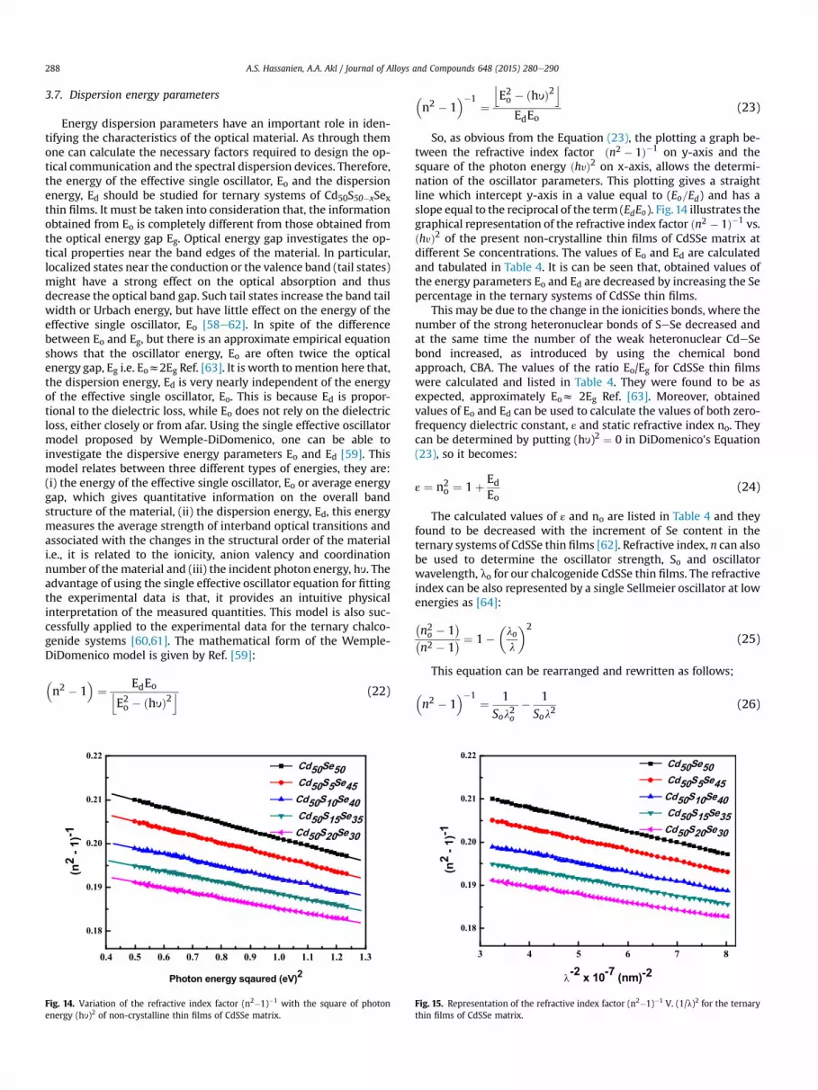
3.7. Dispersion energy parameters
Energy dispersion parameters have an important role in iden-tifying the characteristics of the optical material. As through themone can calculate the necessary factors required to design the op-tical communication and the spectral dispersion devices. Therefore,the energy of the effective single oscillator, Eo and the dispersionenergy, Ed should be studied for ternary systems of Cd50S50�xSexthin films. It must be taken into consideration that, the informationobtained from Eo is completely different from those obtained fromthe optical energy gap Eg. Optical energy gap investigates the op-tical properties near the band edges of the material. In particular,localized states near the conduction or the valence band (tail states)might have a strong effect on the optical absorption and thusdecrease the optical band gap. Such tail states increase the band tailwidth or Urbach energy, but have little effect on the energy of theeffective single oscillator, Eo [58e62]. In spite of the differencebetween Eo and Eg, but there is an approximate empirical equationshows that the oscillator energy, Eo are often twice the opticalenergy gap, Eg i.e. Eoz2Eg Ref. [63]. It is worth tomention here that,the dispersion energy, Ed is very nearly independent of the energyof the effective single oscillator, Eo. This is because Ed is propor-tional to the dielectric loss, while Eo does not rely on the dielectricloss, either closely or from afar. Using the single effective oscillatormodel proposed by Wemple-DiDomenico, one can be able toinvestigate the dispersive energy parameters Eo and Ed [59]. Thismodel relates between three different types of energies, they are:(i) the energy of the effective single oscillator, Eo or average energygap, which gives quantitative information on the overall bandstructure of the material, (ii) the dispersion energy, Ed, this energymeasures the average strength of interband optical transitions andassociated with the changes in the structural order of the materiali.e., it is related to the ionicity, anion valency and coordinationnumber of the material and (iii) the incident photon energy, hy. Theadvantage of using the single effective oscillator equation for fittingthe experimental data is that, it provides an intuitive physicalinterpretation of the measured quantities. This model is also suc-cessfully applied to the experimental data for the ternary chalco-genide systems [60,61]. The mathematical form of the Wemple-DiDomenico model is given by Ref. [59]:
�n2 � 1
�¼ EdEoj
E2o � ðhyÞ2k (22)
0.4 0.5 0.6 0.7 0.8 0.9 1.0 1.1 1.2 1.3
0.18
0.19
0.20
0.21
0.22
(n2 -
1)-1
Photon energy sqaured (eV)2
Cd50Se50 Cd50S5Se45Cd50S10Se40Cd50S15Se35Cd50S20Se30
Fig. 14. Variation of the refractive index factor (n2�1)�1 with the square of photonenergy (hy)2 of non-crystalline thin films of CdSSe matrix.
�n2 � 1
��1 ¼E2o � ðhyÞ2
(23)
j kEdEo
So, as obvious from the Equation (23), the plotting a graph be-tween the refractive index factor ðn2 � 1Þ�1 on y-axis and thesquare of the photon energy ðhyÞ2 on x-axis, allows the determi-nation of the oscillator parameters. This plotting gives a straightline which intercept y-axis in a value equal to (Eo=Ed) and has aslope equal to the reciprocal of the term (EdEo). Fig.14 illustrates thegraphical representation of the refractive index factor ðn2 � 1Þ�1 vs.ðhyÞ2 of the present non-crystalline thin films of CdSSe matrix atdifferent Se concentrations. The values of Eo and Ed are calculatedand tabulated in Table 4. It is can be seen that, obtained values ofthe energy parameters Eo and Ed are decreased by increasing the Sepercentage in the ternary systems of CdSSe thin films.
This may be due to the change in the ionicities bonds, where thenumber of the strong heteronuclear bonds of SeSe decreased andat the same time the number of the weak heteronuclear CdeSebond increased, as introduced by using the chemical bondapproach, CBA. The values of the ratio Eo/Eg for CdSSe thin filmswere calculated and listed in Table 4. They were found to be asexpected, approximately Eoz 2Eg Ref. [63]. Moreover, obtainedvalues of Eo and Ed can be used to calculate the values of both zero-frequency dielectric constant, ε and static refractive index no. Theycan be determined by putting (hy)2 ¼ 0 in DiDomenico's Equation(23), so it becomes:
ε ¼ n2o ¼ 1þ Ed
Eo(24)
The calculated values of ε and no are listed in Table 4 and theyfound to be decreased with the increment of Se content in theternary systems of CdSSe thin films [62]. Refractive index, n can alsobe used to determine the oscillator strength, So and oscillatorwavelength, lo for our chalcogenide CdSSe thin films. The refractiveindex can be also represented by a single Sellmeier oscillator at lowenergies as [64]:
�n2o � 1
��n2 � 1
� ¼ 1��lo
l
�2
(25)
This equation can be rearranged and rewritten as follows;
�n2 � 1
��1 ¼ 1Sol2o
� 1Sol2
(26)
3 4 5 6 7 8
0.18
0.19
0.20
0.21
0.22
(n2 -
1)-1
λ-2 x 10⁻⁷ (nm)-2
Cd50Se50 Cd50S5Se45Cd50S10Se40Cd50S15Se35Cd50S20Se30
Fig. 15. Representation of the refractive index factor (n2�1)�1 V. (1/l)2 for the ternarythin films of CdSSe matrix.

A.S. Hassanien, A.A. Akl / Journal of Alloys and Compounds 648 (2015) 280e290 289
From this equation, if someone plots a graph between therefractive index factor ðn2 � 1Þ�1 on y-axis and the square of thereciprocal of the incident photon wavelengthðlÞ�2 on x-axis, onecan get a straight line of slope equals (1/So) and intercepts y-axis onthe value (1/Solo), as shown in Fig. 15 for thin films of the ternarychalcogenide CdSSe network.
The calculated values of the oscillator strength So and thewavelength of the oscillator were listed in Table 4. From thistable, It can see that, So values are decreased, while values of loare increased by increasing Se percentage in the ternaryCd50S50�xSex matrix. On the other hand, from Wemple-Didome-nico single oscillator parameters (Ed and Eo), one can alsocalculate the moments M-1 and M-3 of the optical spectra for thepresent thin films. These moments were given by the followingequations:
E2o ¼ M�1
M�3and E2d ¼ M3
�1M�3
(27)
Rearrange these equations, one can get:
M�1 ¼ EdEo
and M�3 ¼ M�1
E2o(28)
The calculated values of the moments M�1 and M�3 are given inTable 4. M�1 values were found to be decreased while M�3 valueswere increased with the addition of more Se to thin films of theternary systems of CdSSe. Unfortunately the authors could not getany similar results for non-crystalline CdSSe thin films in theliterature concerned with the refractive index dispersion data aswell as the zero frequency dielectric constant to be compared withour obtained data. But the present data are consonant with the dataof other semiconducting materials [47,55,60e62].
4. Conclusion
� Non-crystalline thermally evaporated thin films of ternarychalcogenide Cd50S50�xSex network (30 � x � 50) have beensuccessfully prepared. The thin films are controlled in to have ahomogenous thickness (200 ± 3 nm).
� The compositional distribution of the constituent elements ofthe chalcogenide thin films of CdSSe matrix was investigatedusing the energy dispersive analysis of X-rays (EDAX), and theywere found much closed to the calculated values.
� Optical absorbance spectra are calculated from the correctedtransmittance and corrected reflectance spectra. The opticalproperties of Cd50S50�xSex thin films were investigated. It wasfound that, the optical band gap for all thin films arose fromindirect optical transitions. The indirect optical band gap, Eg wasfound to decrease while band tail width, EU was increased withthe increase of Se contents in CdSSe network. Obtained resultsare discussed in terms of the chemical bond approach modelCBA.
� The optical density, OD, skin depth, d; extinction coefficient, k,refractive index, n and optical conductivity, s were studied asfunctions of Se content in the thin films of chalcogenide CdSSesystem. These parameters were found to be strongly dependentupon the Se concentration.
� Using the Wemple-DiDomenico single effective oscillatormodel, the dispersion of the refractive index, n and somerelated parameters were calculated and investigated. As aresult, the oscillator energy, Eo dispersion energy, Ed oscillatorstrength, So, oscillator wavelength, lo and zero-frequencyrefractive index (static refractive index, no) were determinedand studied. All these parameters were found to be dependent
also upon the Se content in the ternary chalcogenideCd50S50�xSex thin films.
References
[1] T.D. Rani, K. Tamilarasan, E. Elangovan, S. Leela, K. Ramamurthi, K. Thangaraj,C. Himcinschi, I. Trenkmann, S. SchuIze, M. Hietschold, A. Liebig, G. Salvan,D.R.T. Zahn, Superlattices Microstruct. 77 (2015) 325.
[2] T.M. Razyakov, Thin Solid Films 164 (1998) 301.[3] E.R. Shaaban, Y.A.M. Ismail, H.S. Hassan, J. Non Cryst. Solids 376 (2013) 61.[4] M. Frumar, B. Frumarova, T. Wagner, Amorphous and Glassy Semiconduct.
Chalcogenides, Elsevier, 2011.[5] M. Ali, W.A.A. Syed, M. Zubair, N.A. Shah, A. Mehmood, Appl. Surf. Sci. 284
(2013) 482.[6] A.S. Khomane, Optik 124 (2013) 2432.[7] G.S. Shahane, L.P. Deshmukh, Mater. Chem. Phys. 70 (1) (2001) 112.[8] P.P. Hankare, V.M. Bhuse, K.M. Garadkar, S.D. Delekar, I.S. Mulla, Semicond. Sci.
Technol. 19 (1) (2004) 70.[9] D. Vipin Kumar, K. Dwivedi, Optik 124 (2013) 2345.
[10] K.R. Murali, V. Swaminathan, D.C. Trivedi, Sol. Energy Mater. Sol. Cells 81 (1)(2004) 113.
[11] J.Y. Choi, K.J. Kim, J.B. Yoo, D. Kim, Sol. Energy 64 (1e3) (1998) 41.[12] P. O'Brien, J. McAleese, J. Mater. Chem. 8 (1998) 2309.[13] M. Allias, M. Gardais, Mat. Sci. Eng. B 9 (1991) 429M.[14] R. Bhargava (Ed.), INSPEC Direct, 1997. London.[15] S. Gorer, G. Hodes, J. Phys. Chem. 98 (1994) 5338.[16] M.T.S. Nair, P.K. Nair, R.A. Zingaro, E.A. Meyers, J. Appl. Phys. 74 (1993) 1879.[17] J.B. Choudhari, N.G. Deshpande, Y.G. Gudage, A. Ghosh, V.B. Huse, R. Sharma,
Appl. Surf. Sci. 254 (2008) 6810.[18] R. Mariappan, V. Ponnuswamy, M. Ragavender, Optik 123 (2012) 1196.[19] A.A. Yadav, E.U. Masumdar, J. Alloys Compd. 505 (2010) 787.[20] K.R. Murali, K. Thilakavathy, S. Vasantha, R. Oomen, Chalcogenide Lett. 5
(2008) 165.[21] V. Kumar, T.P. Sharma, J. Phys. Chem. Solids 59 (1998) 1321.[22] S. Pagliara, L. Sangaletti, L.E. Depero, V. Capozzi, G. Perna, Appl. Surf. Sci. 186
(2002) 527.[23] P.K. Kalita, B.K. Sharma, H.L. Das, Ind. J. Phys. 77 (2003) 225.[24] Alaa A. Akl, Inter. J. Mat. Eng. Technol. 8 (2012) 105.[25] S.A. Khan, F.S. Al-Hazmi, S. Al-Heniti, A.S. Faidah, A.A. Al-Ghamdi, Curr. Appl.
Phys. 10 (2010) 145.[26] A. Solieman, M.M. Hafiz, A.A. Abu-Sehly, A.A. Alfaqeer, J. Taibah, Univ. Sci. 01
(2014) 002.[27] A.S. Hassanien, Alaa A. Akl, Physica B 473 (2015) 11.[28] Alaa A. Akl, A.S. Hassanien, Supperlattice Microstruct. 85 (2015) 67.[29] S.A. Fayek, M. El-Ocker, A.S. Hassanien, Mater. Chem. Phys. 70 (2001) 231.[30] B. Jozef, O. Stanford, S. Mahadevan, A. Gridhar, A.K. Singh, J. Non Cryst. Solids
74 (1985) 75.[31] C.M. Muiva, T.S. Sathiaraj, J.M. Mwabora, Eur. Phys. J. Appl. Phys. 59 (2012)
10301.[32] R.T. Sanderson, J. Am. Chem. Soc 105 (1983) 2259.[33] L. Pauling, J. Am. Chem. Soc. 54 (1932) 3570.[34] F. Demichelis, G. Kanidakis, A. Tagliferro, E. Tresso, Appl. Opt. 9 (26) (1987)
1737.[35] A. Sharma, N. Mehta, A. Kumar, J. Mater. Sci. 46 (2011) 4509.[36] S.I. Cordoba-Torresi, A. Hugot-Le Goff, S. Joiret, J. Electrochem. Soc. 138 (1991)
1554.[37] J. Tauc, in: J. Tauc (Ed.), Amorphous and Liquid Semiconductors, Plenum Press,
London and New York, 1974.[38] E.A. Davis, N.F. Mott, Philos. Mag. 22 (1970) 903.[39] G.S. Shahane, B.M. More, C.B. Rotti, L.P. Deshmukh, Mater. Chem. Phys. 47
(1997) 263.[40] R. Mariappan, V. Ponnuswamy, M. Ragavendar, Optic 123 (2012) 1196.[41] A.A. Yadav, E.U. Masumdar, Mat. Res. Bull. 45 (2010) 1455.[42] F.I. Ezema, R.U. Osuji, Chalcogenide Lett. 4 (2007) 69.[43] D. Bhattacharya, S. Chaudhuri, A.K. Pal, Vacuum 43 (1992) 313.[44] M.A. Majeed Khan, M.W. Khan, J. Alloys Compd. 486 (2009) 876.[45] L. Pauling, The Nature of the Chemical Bond, third ed., Cornell University
Press, Ithaca, NY, 1960.[46] J. Tauc, R. Grigorovici, A. Vancu, Phys. Stat. Sol. 15 (1966) 627.[47] A. Dahshan, K.A. Aly, J. Non Cryst. Solids 408 (2015) 62.[48] A.L. Allred, J. Inorg. Nucl. Chem. 1 (1961) 215.[49] S.A. Fayek, J. Phys. Chem. Solids 62 (2001) 653.[50] S.A. Fayek, S.M. El Sayed, J. Phys. Chem. Solids 63 (2002) 1.[51] J.F. Eloy, Power Lasers National Sch. Phys., John Wiley and Sons, Grenoble,
France, 1984.[52] S.S. Chiad, Inter.letter Chem. Phys. Astro 6 (2015) 50.[53] N.F. Habubi1, S.F. Oboudi, S.S. Chiad, J. Nano Electron. Phys. 4 (2012)
4008.[54] N.F. Mott, E.A. Davis, Electronic Processes in Non-Crystalline Materials, Clar-
endon, Oxford, 1979.[55] S.A. Mahmoud, A.A. Akl, S.M. Al-Shomar, Physica. B 404 (2009) 2151.[56] O.S. Heavens, Optical Properties of Thin Solid Films, Dover, New York,
1965.

A.S. Hassanien, A.A. Akl / Journal of Alloys and Compounds 648 (2015) 280e290290
[57] S.A. Mahmoud, Egypt J. Sol. 19 (1996) 221.[58] P. Sharma, A. Dahshan, K.A. Aly, J. Alloys Compd. 616 (2014) 323.[59] S.H. Wemple, M. Didomenico, Phys. Rev. B 3 (1971) 1338.[60] I. Solomen, M.P. Schmidt, C. Senemaud, M.D. Khodja, Phys. Rev. B38 (1988)
13263.
[61] H.S. Shaaker, W.A. Hussain, H.A. Badran, Adv. Appl. Sci. Res. 3 (5) (2012) 2940.[62] K. Goksen, N.M. Gasanly, H. Ozkan, Acta Phys. Pol. A 112 (2007) 93.[63] K. Tanaka, Thin Solid Films 66 (1980) 271.[64] A.K. Walton, T.S. Moss, Proc. Phys. Soc. 81 (1963) 509.
Copyright © 2022 FDOKUMEN