Biospecific fractionation matrices for sequence specific endonucleases
Upload
khangminh22Category
view
3download
0
Università degli Studi di Cagliari
PHD DEGREE
Physics
Cycle XXXII
Impregnation of porous silicon matrices for
technological applications
Scientific Disciplinary Sector(s)
FIS/01
PhD Student Elisa Pinna
Coordinator of the PhD Programme Prof. Paolo Ruggerone
Supervisor Dott. Guido Mula
Final exam. Academic Year 2018 – 2019
Thesis defence: January-February 2020 Session

i
To myself and who was, is and always will be by my side.

ii
Elisa Pinna gratefully acknowledges Sardinian Regional Government forthe financial support of her PhD scholarship (P.O.R. Sardegna F.S.E. -Operational Programme of the Autonomous Region of Sardinia, EuropeanSocial Fund 2014-2020 - Axis III Education and training, Thematic goal 10,Investment Priority 10ii), Specific goal 10.5.

Abstract
iii

iv
This PhD thesis presents a study of the filling of porous silicon matrices andhas been done prevalently in the laboratory PoroSiLab, of the Department ofPhysics of the University of Cagliari.
Porous silicon (PSi) is a very versatile material, whose main feature is thelarge developed surface. This inner surface, generated by the presence ofpores, makes PSi particularly suitable for applications needing pores impreg-nation. In this way, many new different systems can be formed, and theircharacteristics can be exploited for several technological applications. PSi,beneath its complex nature, is very attractive in many different technologicalfields, from energy storage and production, sensors and optoelectronic devicesand biomedical applications. Many research efforts have been done for theoptimization of these kind of devices, including the optimization of poresimpregnation mechanisms, aiming at the improvement of the performances ofthe final structures.In this PhD thesis I will report a study on the impregnation of PSi withdifferent materials for a variety of technological applications. In particular,the impregnation process has been studied for organic and inorganic materials,with the aim of optimizing the process and, as a consequence, the samplesproperties.In the first part of this study, the chemical impregnation of the PSi matrix withmelanin will be presented. After a brief introduction on the past discoverieson the hybrid junction, I will present the results in the understanding of themechanisms governing the penetration of melanin starting monomers andtheir polymerization into melanin, together with the improvement we achievedin increasing the lifetime of the hybrid structure in terms of production ofphotogenerated current. I will also present the results obtained using adifferent PSi matrix, that is a porous structure obtained by using metal-assisted chemical etching (MACE). The MACE approach has been usedto limit the high Si reflectivity by a suitable surface structurations. Theimpregnation of MACE-formed structures with melanin is then aimed atan increase of the photovoltaic properties lead by the increased light powerentering the MACE-based structures.

v
The second part of the project regards the PSi impregnation with inorganicmaterials using an electrochemical approach for the impregnation of theporous matrix with erbium and nickel. Erbium has been chosen because ofits demonstrated photoluminescence (PL) properties when hosted in a siliconmatrix; the interest on this topic has started to decrease when it has beenfound that erbium clustering limits the PL emission. In this thesis I will showby a wide multidisciplinar study that pores filling, instead of the standardpores doping approach, can be a promising route to overcome the erbiumclusters formation and to enhance the PL intensity. The impregnation of PSiwith nickel has a different goal and is aimed at the fabrication of a multiphasematerial that can be used to define a valid protocol for the analysis andaccurate reconstruction of nanoporous materials with atom probe tomography(APT), a technique lacking of a reliable approach for the definition of accuratereconstruction parameters. The main characteristic of this particular pair ofmaterials is that silicon and nickel have similar evaporation fields, which isessential to perform the analysis of porous composite materials with APT.Despite the different materials and the various technological applicationsof the analyzed samples, the common feature of the work is the study ofthe impregnation processes. A good understanding of the impregnationprocess is the base for the optimization of the final device. The understandingand control of the parameters governing the filling of meso- and nano-poresis in fact a very complex matter that is unavoidably influenced by manyenvironmental parameters (temperature, humidity...) that can be difficultto control properly. For these reasons, my PhD work has been aimed at theunderstanding of what parameters are fundamental for a successful poresimpregnation and why. Although part of the parameters involved necessarilydiffer for an impregnation with organic and inorganic materials, many arenonetheless related for both kinds materials to size, shape, regularity of thepores distribution, and their knowledgeable control is therefore essential for awide variety of application.This work has been done within a collaboration with many national andinternational research groups. As previously mentioned, most of my workwas done in the laboratory PoroSiLab. I was in charge of the fabrication

vi
and impregnation of the PSi samples, of their characterization by means ofreflectivity and absorbance analysis and of all the photocurrent measurements.The computational analysis presented in the text, aimed at understanding thepolymerization of melanin monomers and the adhesion on a silicon surface,have been carried out by the groups of L. Colombo and G. Cappellini of thesame university, while melanin monomers were synthesized at the UniversityFederico II of Napoli by the group of M. d’Ischia. I also fabricated the PSisamples with the MACE technique during a four months international stageat CNRS-ICMPE laboratories in Thiais (France), where I also performedtheir impregnation with the organic material and all the analysis on thosesamples. I participated to the PL analysis of the Er-filled porous Si samplesthat have been carried out by the group of M. Saba of the University ofCagliari. The scanning electron microscope (SEM) images, also using back-scattering electrons (SEM-BSE) and energy dispersive X-Ray spectroscopy(SEM-EDS), of these samples have been taken by the group of A. Falqui atKAUST (Saudi Arabia). Electron tomography (ET) and micro-PL analysison Er-doped samples and APT and ET on samples impregnated with nickelhave been performed in the laboratories of the Université Grenoble Alps andCEA, LETI, MINATEC Campus. Our collaborators from INRIM (Torino)performed SEM analysis of PSi and allowed us to develop the ElectrochemicalNanolithography (ENL) technique for samples fabrication, characterized bymore regular and larger pores.Most of the results of this thesis have been published in the following articlesin international journals:
• E. Pinna, M. Mehrabanian, E. Redolfi Riva, E. Cara, G. Aprile, L.Boarino, G. Mula, Electrochemical Nanolithography on silicon: aneasy and scalable method to control pores formation at the nanoscale,Materials 2019, 12, 18, 2891
• A. Antidormi, G. Aprile, G. Cappellini, E. Cara, R. Cardia, L. Colombo,R. Farris, M. d’Ischia, M. Mehrabanian, C. Melis, G. Mula, A. Pezzella,E. Pinna, E. Redolfi Riva, Physical and chemical control of interfacestability in porous silicon-eumelanin hybrids, J. Phys. Chem. C 2018,
vii
122, 49, 28405-28415
• E. Pinna, C. Melis, A. Antidormi, R. Cardia, E. Sechi, G. Cappellini,M. d’Ischia, L. Colombo, G. Mula, Deciphering molecular mechanismsof interface buildup and stability in porous Si/eumelanin hybrids, Int.J. Mol. Sci. 2017, 18(7), 1567
• G. Mula, T. Printemps, C. Licitra, E. Sogne, F. D’Acapito, N. Gam-bacorti, N. Sestu, M. Saba, E. Pinna, D. Chiriu, P. C. Ricci, A. Casu,F. Quochi, A. Mura, G. Bongiovanni, A. Falqui, Doping porous siliconwith erbium: pores filling as a method to limit the Er-clustering effectsand increasing its light emission, Scientific Reports 2017 7, 5957
• I. Mouton, T. Printemps, A. Grenier, N. Gambacorti, E. Pinna, M.Tiddia, A. Vacca, G. Mula, Toward an accurate quantification in atomprobe tomography reconstruction by correlative electron tomographyapproach on nanoporous materials, Ultramicroscopy 2017, 182, 112-117
The results obtained and discussed in this thesis have also been presented inthe following national and international conferences and events:
• European School on Nanosciences and Nanotechnologies - ESONN(2018):
– Poster: Nanostructured porous silicon for technological applica-tions.
• Porous Semiconductors Science and Technology - PSST (2018):
– Oral: A new paradigm for PSi:Er light-emitting structures
– Posters: Deciphering molecular mechanism of interface buildupand stability in porous Si/eumelanin hybrids
– Electrochemical nanolithography on highly-doped porous silicon
• XI International School On Hybrid and Organic Photovoltaics and IVSchool on Advanced Materials for Photonics, Electronics and Bioelec-tronics - ISOPHOS & MAPHEBIO (2019):

viii
– Poster: Organic-inorganic hybrids of eumelanin and porous Si:how to improve the junction stability
• 8th Young Researcher Meeting - YRM (2017):
– Oral: Organic-inorganic hybrids of eumelanin and porous silicon:how to improve the junction stability
– Poster: Porous silicon/polyaniline hybrid materials for photovoltaicapplications
• 79th IUVSTA workshop (2017):
– Poster: Accurate quantification in atom probe tomography recon-struction by correlative electron tomography approach on nanoporousmaterials
• E-MRS Spring Meeting (2016):
– Oral: Organic-inorganic hybrids of eumelanin and porous Si: to-ward stable photocurrents
• Porous Semiconductors Science and Technology - PSST (2016):
– Posters: Eumelanin-porous silicon hybrids: towards stable pho-tocurrent
– Atomistic characterization of the hybrid eumelanin-porous siliconinterface: a molecular dynamics study

Contents
I State of the art 1
1 Porous materials impregnation 2
1.1 Overview of porous materials impregnation . . . . . . . . . . . 21.2 A more specific case: porous silicon impregnation . . . . . . . 4
2 Porous silicon matrices 6
2.1 Porous silicon . . . . . . . . . . . . . . . . . . . . . . . . . . . 62.1.1 Anodic etching . . . . . . . . . . . . . . . . . . . . . . 82.1.2 Metal-assisted chemical etching . . . . . . . . . . . . . 11
3 Organic and inorganic materials to fill a porous matrix 13
3.1 Melanin: an organic material for hybrid photovoltaic hetero-junctions . . . . . . . . . . . . . . . . . . . . . . . . . . . . . . 13
3.2 Erbium: an inorganic material for silicon-based photolumines-cence devices . . . . . . . . . . . . . . . . . . . . . . . . . . . 16
3.3 Nickel: an inorganic material for a better understanding ofporous matrices impregnation . . . . . . . . . . . . . . . . . . 19
II Methods 20
4 Fabrication and measurement methods 21
4.1 Fabrication of the substrates . . . . . . . . . . . . . . . . . . . 214.1.1 Electrochemical etching . . . . . . . . . . . . . . . . . 214.1.2 Metal-assisted chemical etching . . . . . . . . . . . . . 23
4.2 Impregnation of the substrates . . . . . . . . . . . . . . . . . . 24
ix

CONTENTS x
4.2.1 Porous silicon filling with melanin . . . . . . . . . . . . 244.2.2 Porous silicon doping with erbium . . . . . . . . . . . . 254.2.3 Porous silicon filling with nickel . . . . . . . . . . . . . 25
4.3 Structural characterization . . . . . . . . . . . . . . . . . . . . 254.3.1 SEM . . . . . . . . . . . . . . . . . . . . . . . . . . . . 264.3.2 Electron tomography . . . . . . . . . . . . . . . . . . . 26
4.4 Samples measurements . . . . . . . . . . . . . . . . . . . . . . 274.4.1 Photocurrent measurements . . . . . . . . . . . . . . . 274.4.2 Photoluminescence measurements . . . . . . . . . . . . 28
III Results and discussion 30
5 Porous silicon impregnated with melanin 31
5.1 Thin-pores samples with eumelanin . . . . . . . . . . . . . . . 315.2 Electrochemical Nanolithography for larger pores fabrication . 505.3 Large-pores samples with eumelanin . . . . . . . . . . . . . . . 615.4 MACE nanostructured porous silicon with eumelanin . . . . . 64
6 Porous silicon impregnated with erbium 69
6.1 A little background on Er-doped PSi: photoluminescence in-tensity issue . . . . . . . . . . . . . . . . . . . . . . . . . . . . 69
6.2 A new approach: pores filling for photoluminescence improvement 726.3 Er-doping of large-pores samples . . . . . . . . . . . . . . . . . 82
7 Porous silicon impregnated with nickel 86
7.1 Nickel in porous silicon for a better atom probe tomographyreconstruction . . . . . . . . . . . . . . . . . . . . . . . . . . . 86
Conclusion 93
Bibliography 97
Acknowledgements 122

Part I
State of the art
1

Chapter 1
Porous materials impregnation
In this chapter, a general introduction to the main topic of this dissertation,that is the impregnation of a porous silicon (PSi) matrix, is presented. Section1.1 will give the reader an overview of porous materials impregnation and thephysical aspects related to that; then, in section 1.2, the impregnation issueis treated for the specific case of PSi.
1.1 Overview of porous materials impregnation
The impregnation of a porous matrix can be generally described by thephysical laws of capillarity [1, 2], which occurs when a liquid flows in narrowtubes without the assistance of external forces like gravity, and sometimes evenin opposition to that. Capillarity is the result of two forces, the adhesion of theliquid to solid surfaces and the cohesive surface tension of liquid molecules;these are in opposition one another since the former tends to spread theliquid and the latter tends to reduce the liquid-gas interfacial area. Thefinal liquid-gas interface configuration is found through a balance betweenthese forces. Capillarity is thus dependent on solid and liquid interfacialproperties such as surface tension, contact angle, and solid surface roughnessand geometry [3]. Surface tension derives from the fact that fluid molecules atthe air-fluid interface are subjected to a net attraction force from bulk liquidmolecules. Bulk molecules, in contrast, experience uniform cohesive forces
2
CHAPTER 1. POROUS MATERIALS IMPREGNATION 3
from whatever direction. As a result, a membrane-like fluid surface appears,and it tends to contract to reduce the amount of its excess surface energy.Surface tension depends on the liquid and can be modified by the additionof soluble substances. Temperature also affects surface tension, because thecohesive forces between molecules are reduced in case of thermal expansion:in general, therefore, the experimental conditions of impregnation are a verydelicate factor. The impregnation of a surface also depends on the wettabilityof that surface. From this point of view, a significative parameter is thecontact angle, that is the equilibrium angle formed between the solid-liquidinterface and the liquid-gas interface. According to this definition, a solidis called wettable by the liquid when the contact angle is small (figure 1.1(a)) and it happens when liquids molecules are attracted to solid surfacesmore strongly than to the other liquid molecules. Conversely, a solid is callednot-wettable by the liquid when the contact angle is large (figure 1.1 (b))because the cohesive force among the molecules within the liquid is largerthan the adhesive force of the solid. Another factor that affects impregnationis surface geometry. In fact, the final liquid-gas interface is the result of abalance between the forces that tend to spread the liquid and surface tension,which tends to minimize interfacial area within the pore. For these reasons,the final interface between the liquid and the gas phases is often curved.A hemispherical interface would be the ideal shape in case of regular solidmatrices, while a not-spherical shape is much more common when the liquidis confined by irregular solid surfaces.

CHAPTER 1. POROUS MATERIALS IMPREGNATION 4
!"#
!#$
!$"
!#$
!"#!$"%%
(a) (b)
Figure 1.1: Different solid-liquid-gas contact angles: (a) small contact angle(� < 90° defines a wettable solid); (b) large contact angle (� > 90° defines anot-wettable solid).
1.2 A more specific case: porous silicon impreg-
nation
PSi is at the base of this dissertation and the study of its impregnation isof particular interest since it permits to tune PSi properties or to developcomposite structures with new interesting characteristics. In the secondhalf of the 90s of the last century, for example, several groups tried toimpregnate PSi to improve or modify its luminescence properties [4–6], butmany other applications aimed at the investigations of PSi impregnation withdifferent materials. Some years later, the filling of PSi has been studied forelectronic devices, like the fabrication of an X-ray imaging pixel detector [7]or the realization of microchannels in heat sink technology [8]. Impregnationwith magnetic materials has been proposed by the group of P. Granitzerand a relation between the structure and magnetic characteristics has beendemonstrated [9–11]. New results on this topic have been found in the lastyears [12–14]. Impregnation of PSi with organic materials is another fieldof interest, both for exploiting the properties of the new composites [15–18]and to use the porous matrix as a template to prepare defined arrays of theorganic compound [19–21]. These are only some examples, but many othercases can be found in literature [22–26]. Among the various ways to achievePSi filling, chemical and electrochemical impregnation processes have beenused in this dissertation, and a brief description of these methods will begiven below.

CHAPTER 1. POROUS MATERIALS IMPREGNATION 5
Chemical pores impregnation consists in putting the PSi sample in directcontact with a solution of the material to be deposited inside the pores,and let the solvent to evaporate, without using any current. This techniqueis often used for the insertion of metals or polymers [27], but the successof the process depends on chemical and morphological properties of thesurface. In fact, a freshly etched SiHx -terminated PSi is hydrophobic and itshould be chemically modified to optimize the impregnation with hydrophilicsubstances [28]. Another procedure used for polymer impregnation is tospread the polymer solution over the porous surface by spin-coating; in thiscase, viscosity and rotation speed are important parameters for the success ofthe pores impregnation. This technique has been used also in this dissertationfor impregnation of PSi with melanin, and the results are presented in sections5.1 and 5.3. In case of the insertion of metals, the process is usually theresult of redox reactions where both the metal formation and the silicon atomoxidation occur. For this reason, the reaction is inhibited after the depositionof one or two monolayers, since the silicon atoms are all covered by the newmaterial.Electrochemical impregnation, instead, is a technique that involves electro-chemical reactions inside the pores between silicon and the material dissolvedin the solution. The impregnation results strongly depend on the morpho-logical structure of the porous matrix: if for macropores is easy to obtaina homogenous in-depth filling [29], gradients are often observed in case ofmesoporous and nanoporous materials [30]. This is probably due to poresshapes, especially when they are dendritic. In fact, an irregular pore shapemay lead to pore obstruction due to an irregular electrodeposition of materialslead by inhomogeneous flow of the electrolyte within the complex dendriticpore net. Other reasons for pore-blocking could be an insufficient exchangeof the electrolyte along the entire pore length or hydrogen bubbles formationduring the reaction. In any case, in the work presented in reference [31] ithas been shown that pores filling is also related on current density and onpulse duration, so that to obtain good results a careful optimization of theprocess is a mandatory preliminary step.
Chapter 2
Porous silicon matrices
In this chapter I will provide a general introduction on PSi and on the varioustechniques used for producing the porous matrices studied in this dissertation.In particular, after a brief introduction on PSi characteristics and properties insection 2.1, the theory of the anodic etching is presented in section 2.1.1, whilesection 2.1.2 is dedicated to the explanation of the so-called Metal-AssistedChemical Etching (MACE).
2.1 Porous silicon
PSi discovery dates back to the 1950s at Bell Laboratories, when the scientistsArthur Jr. and Ingeborg Uhlir were studying an electrochemical techniquefor polishing and shaping the surfaces of silicon and germanium in order touse them in microelectronic circuits. They noted that, under appropriateelectrochemical conditions, some black, brown or red films on the surface ofthe substrates were formed [32]. Since they were not interested in that effect,they adjusted the experimental conditions to prevent this effect and reportedthe unusual result in a Bell labs note.For several decades PSi discovery remained shelved, until the beginning ofthe 90s, when the interest in this material arose thanks to the independentdiscovery, by the scientists L. Canham and V. Lehmann, of its photolumines-cence (PL) in the visible band, that is at energies significantly higher than
6
CHAPTER 2. POROUS SILICON MATRICES 7
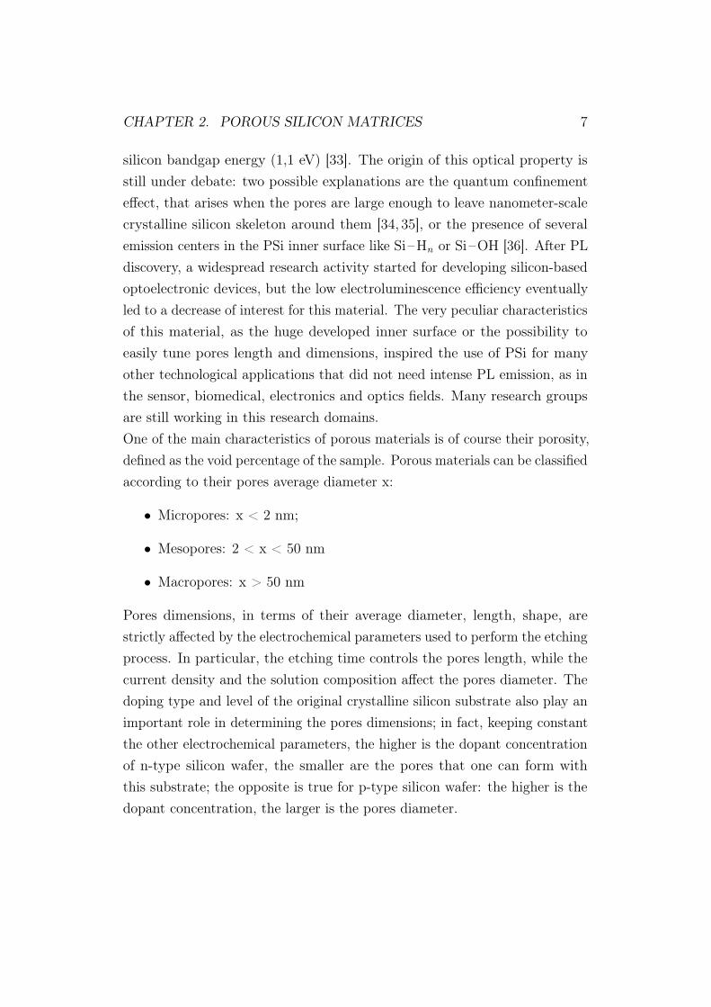
silicon bandgap energy (1,1 eV) [33]. The origin of this optical property isstill under debate: two possible explanations are the quantum confinementeffect, that arises when the pores are large enough to leave nanometer-scalecrystalline silicon skeleton around them [34, 35], or the presence of severalemission centers in the PSi inner surface like Si–Hn or Si–OH [36]. After PLdiscovery, a widespread research activity started for developing silicon-basedoptoelectronic devices, but the low electroluminescence efficiency eventuallyled to a decrease of interest for this material. The very peculiar characteristicsof this material, as the huge developed inner surface or the possibility toeasily tune pores length and dimensions, inspired the use of PSi for manyother technological applications that did not need intense PL emission, as inthe sensor, biomedical, electronics and optics fields. Many research groupsare still working in this research domains.One of the main characteristics of porous materials is of course their porosity,defined as the void percentage of the sample. Porous materials can be classifiedaccording to their pores average diameter x:
• Micropores: x < 2 nm;
• Mesopores: 2 < x < 50 nm
• Macropores: x > 50 nm
Pores dimensions, in terms of their average diameter, length, shape, arestrictly affected by the electrochemical parameters used to perform the etchingprocess. In particular, the etching time controls the pores length, while thecurrent density and the solution composition affect the pores diameter. Thedoping type and level of the original crystalline silicon substrate also play animportant role in determining the pores dimensions; in fact, keeping constantthe other electrochemical parameters, the higher is the dopant concentrationof n-type silicon wafer, the smaller are the pores that one can form withthis substrate; the opposite is true for p-type silicon wafer: the higher is thedopant concentration, the larger is the pores diameter.
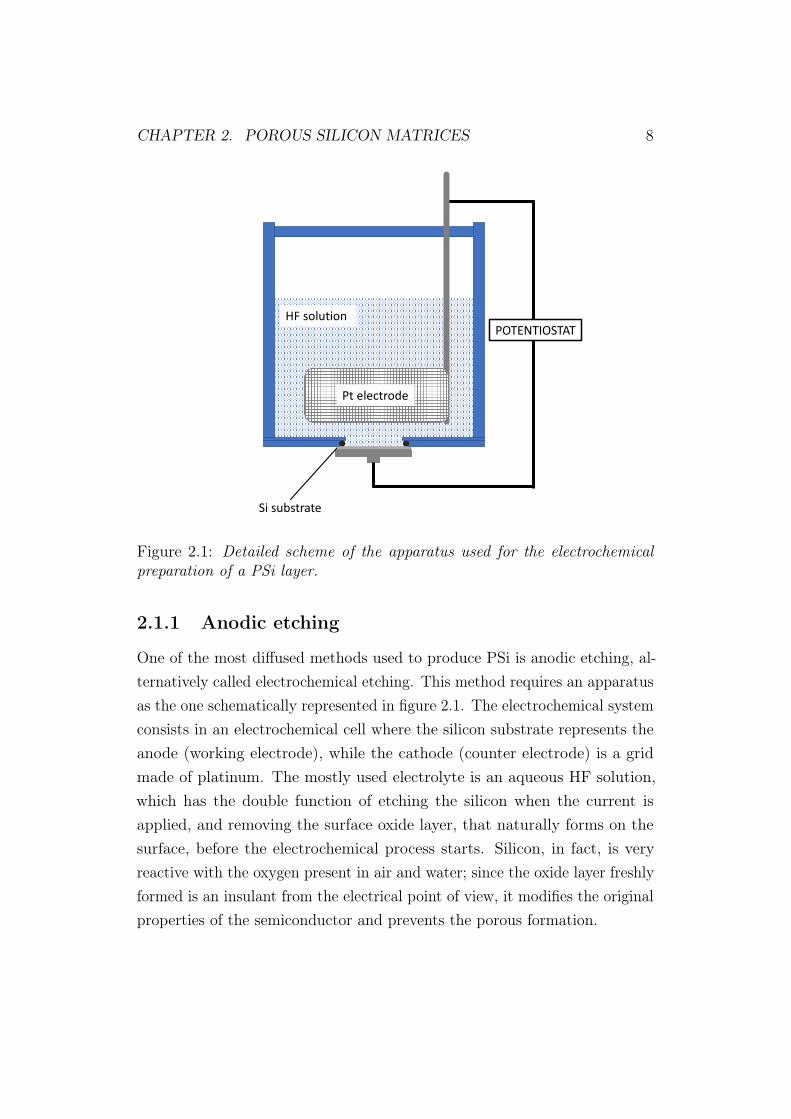
CHAPTER 2. POROUS SILICON MATRICES 8
POTENTIOSTATHF solution
Pt electrode
Si substrate
Figure 2.1: Detailed scheme of the apparatus used for the electrochemicalpreparation of a PSi layer.
2.1.1 Anodic etching
One of the most diffused methods used to produce PSi is anodic etching, al-ternatively called electrochemical etching. This method requires an apparatusas the one schematically represented in figure 2.1. The electrochemical systemconsists in an electrochemical cell where the silicon substrate represents theanode (working electrode), while the cathode (counter electrode) is a gridmade of platinum. The mostly used electrolyte is an aqueous HF solution,which has the double function of etching the silicon when the current isapplied, and removing the surface oxide layer, that naturally forms on thesurface, before the electrochemical process starts. Silicon, in fact, is veryreactive with the oxygen present in air and water; since the oxide layer freshlyformed is an insulant from the electrical point of view, it modifies the originalproperties of the semiconductor and prevents the porous formation.

CHAPTER 2. POROUS SILICON MATRICES 9
Figure 2.2: Reaction scheme for the divalent model of the porosificationprocess [37].
On the base of the electronegativity values of the elements, the enthalpy ofSi–F is higher than the enthalpy of Si –O, so the HF solution easily dissolvesthe oxide layer, according to the following reaction:
SiO2+ 6HF ! SiF2�
6+ 2H+ + 2H
2O
Once the oxide layer has been removed, superficial silicon is now passivatedby Si–H bonds and the porosification process can occur. The charge transferreaction that led to the removal of the surface silicon atoms is a divalentmechanism (figure 2.2). The dissolution process starts when a hole that travelsinside the crystal reaches the interface between silicon and the electrolyte. Thisfavors the nucleophilic attack of the silicon atom by bifluoride ions (HF2
– ),and the new Si–F bond is formed. At this point, another nucleophilic attackcan occur on the same Si atom, with the injection of an electron as a result:this leads to the formation of a second Si–F bond and to the emission of agaseous H2 molecule. Because of the polarity of the Si–F bonds, the electrondensity of the remaining two silicon backbonds is weakened, and facilitatesthe dissolution of the Si atom by HF. The overall reaction of the divalentporosification process is the following:
Si + 4HF�2+ h+ ! SiF2�
6+ 2HF + H
2+ e�
PSi formation can occur only for particular condition of the electrical param-eter, as it shows the graph in figure 2.3, that connects the current density

CHAPTER 2. POROUS SILICON MATRICES 10
Figure 2.3: Evolution of Si electrochemical etching depending on the currentdensity and the applied tension between the electrodes [38].
flowing in the cell with the potential applied between the electrodes.
Three different regions can be distinguished:
• the first region, corresponding to low values of the applied potential,is the effective region where the PSi formation occurs, with the onlyrestriction that the applied potential must be higher than the opencircuit potential (OCP), otherwise no current can circulate between theelectrodes;
• in the second region the silicon porosification continues and the porouslayer becomes very fragile;
• the third region is the so-called "electropolishing-region", where ithappens that the porous layer is no more there because the siliconatoms are uniformly removed from the layer.

CHAPTER 2. POROUS SILICON MATRICES 11
2.1.2 Metal-assisted chemical etching
Metal-assisted chemical etching is an alternative way to produce PSi withoutusing any external current or voltage. The first demonstration of this methodfor Si etching dates back to 1997, when PSi was fabricated starting froman Al-coated silicon substrate immersed in a solution of HF, HNO3 andH2O [39]. Reports on the use of metal-assisted chemical etching are alsopresent for GaAs, GaN and SiC [39]. This method uses the combined actionof noble metals like Al, Ag, Au, Pd, Pt, Fe or Au–Pd alloys, and a solution ofhydrofluoric acid and a mild oxidizing agent (such as H2O2, HNO3, KMnO4
or HClO4). The metals are deposited as films or nanoparticles in the siliconsurface and act as catalysts in the pores formation, accelerating the etchingeffect of the oxidizing agents. Depending on the conditions, the corrosion canoccur either immediately below the metal catalyst [40,41], giving a very goodspatial control, or also everywhere around it [42, 43]. Generally speaking, themechanism of the etching method can be described as follows [44]. Suppose tohave a MACE system where a silicon substrate is coated with a gold catalystfilm, and H2O2 has been used as the oxidizing agent. In this system, a hole isinjected from the metal into the silicon, oxidizing it according to the followingreaction:
H2O
2+ 2H+
Au���! 2H
2O+ 2h+
The oxidized material reacts with hydrofluoric acid to form soluble siliconhexafluoride and gaseous hydrogen. The etching reaction is reported hereafter,while figure 2.4 represents the graphic scheme of the process.
Si + 4HF�2+ 2h+ ! SiF2�
6+ 2HF + H
2

CHAPTER 2. POROUS SILICON MATRICES 12
Si
Au
H+
h+
H2SiF6HF H2H2O2 H2O
Figure 2.4: Graphic scheme of silicon etching according to metal-assistedchemical etching.
Chapter 3
Organic and inorganic materials
to fill a porous matrix
In this chapter an overview on the materials that have been used to impregnatethe PSi matrix is presented, with a focus on their characteristics and propertiesthat led to their choice for this research. In section 3.1 some information onthe origin and the main properties of melanin is given; section 3.2 reportsthe main characteristics of erbium, esccpecially when it is used to producea silicon-based photoluminescent structure; finally section 3.3 describes themain properties of Ni with respect to the application studied here.
3.1 Melanin: an organic material for hybrid
photovoltaic heterojunctions
Melanin is a light-absorbing polymer commonly known as the dark pigmentthat gives the colour to human skin, but it is also regarded by researchersas one of the most enigmatic biopolymers existing in nature [45]. Severalclassifications have been proposed for melanins; R. A. Nicolaus in 1964suggested a classification of melanins into three main groups [46]: eumelanins,pheomelanins and allomelanins. The first two groups include animal pigments,while the latter includes dark non-nitrogenous pigments found in plants, fungiand bacteria. A more recent definition has been proposed in 1995 by G.
13
CHAPTER 3. ORGANIC AND INORGANIC MATERIALS TO FILL A POROUS MATRIX14
NH
HO
HO
DHI
NH
HO
HO
COOH
DHICA
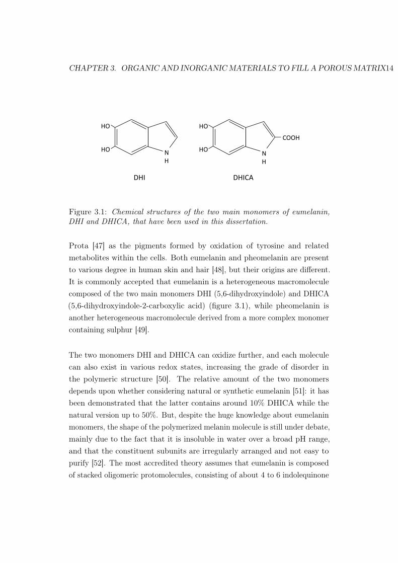
Figure 3.1: Chemical structures of the two main monomers of eumelanin,DHI and DHICA, that have been used in this dissertation.
Prota [47] as the pigments formed by oxidation of tyrosine and relatedmetabolites within the cells. Both eumelanin and pheomelanin are presentto various degree in human skin and hair [48], but their origins are different.It is commonly accepted that eumelanin is a heterogeneous macromoleculecomposed of the two main monomers DHI (5,6-dihydroxyindole) and DHICA(5,6-dihydroxyindole-2-carboxylic acid) (figure 3.1), while pheomelanin isanother heterogeneous macromolecule derived from a more complex monomercontaining sulphur [49].
The two monomers DHI and DHICA can oxidize further, and each moleculecan also exist in various redox states, increasing the grade of disorder inthe polymeric structure [50]. The relative amount of the two monomersdepends upon whether considering natural or synthetic eumelanin [51]: it hasbeen demonstrated that the latter contains around 10% DHICA while thenatural version up to 50%. But, despite the huge knowledge about eumelaninmonomers, the shape of the polymerized melanin molecule is still under debate,mainly due to the fact that it is insoluble in water over a broad pH range,and that the constituent subunits are irregularly arranged and not easy topurify [52]. The most accredited theory assumes that eumelanin is composedof stacked oligomeric protomolecules, consisting of about 4 to 6 indolequinone

CHAPTER 3. ORGANIC AND INORGANIC MATERIALS TO FILL A POROUS MATRIX15
units, as large as 15 to 20 Å and with an interplanar distance of 3.4Å;this theory has been demonstrated through scanning electron microscopymeasurements by the group of G. W. Zajac [53]. In this study, the focus ison eumelanin and on its optical and conductive properties, since this organicmaterial has been used as an absorbent material for photovoltaic applications.Particularly interesting is the absorption spectrum of a eumelanin film; asit is visible from figure 3.2, it is a broad-band, continuous and monotonicabsorption spectrum, more like an inorganic material than an organic one.In fact, the curve can be fitted with a single exponential (as in the insert)and the total absence of any peaks corresponding to transitions betweendistinct electronic states and/or satellite vibronic states is visible. For thischaracteristic, it has been proposed to describe melanin with a bandedsemiconductor model, according to which every monomer has discrete energylevels; as the monomers link together to form polymers, the energy levelsbecome denser and denser and close up to form continuous energy bands.There exist the HOMO (Highest Occupied Molecular Orbital) and LUMO(Lowest Unoccupied Molecular Orbital) orbitals, that correspond to the top ofvalence band and the bottom of conduction band in organic semiconductors,respectively.
The most diffused theory to explain eumelanin absorption spectrum is relatedto scattering; reference [55] reports that the natural pigment in particle formmust be characterized by Mie and Rayleigh scattering. The latter dependsfrom radiation wavelength as ��4 and occurs when particles dimensions aremuch lower than incident wavelength (e.g. tens of nanometers); accordingwith computational calculations [56] it should cause the stiff increase of thespectrum for � < 300 nm. The former, instead, happens when radiation inter-acts with particles in the micron-range; it has no dependence on wavelength,but can contribute to the melanin absorbance spectrum since it superimposesa broad background on any absorption spectrum. However, it is worth to saythat the broad spectrum evolves during the oxidative coupling of precursorssuch as DHICA or DHI [57], when the oxidative breakdown of the pigmentoccurs [58], or when low molecular fraction are isolated [59]. In this disser-

CHAPTER 3. ORGANIC AND INORGANIC MATERIALS TO FILL A POROUS MATRIX16
Figure 3.2: Monotonic, broad band UV-Visible absorption spectrum of asynthetic film of eumelanin. In the insert, the fit with a single exponentialand the absence of distinct chromophoric peaks are visible [54].
tation, a contribution in the understanding of the polymerization of thesemolecules and a study of a hybrid diffused heterojunction made of eumelaninand PSi are presented [60,61].
3.2 Erbium: an inorganic material for silicon-
based photoluminescence devices
Erbium is one of the 17 elements that constitute the class of rare earths,all of them characterized by three valence electrons. These elements comepredominantly from USA and China and, after their extraction, separationand purification, they are commercialized as oxides, carbonates, chlorides,fluorides, borides, hydroxides or as pure metals or alloys. The application fieldsspan from the production of computer and television screens, to optical fibers,transistors [62] and rods for nuclear reactors [63]. Erbium is an interestingmaterial for the optical luminescent properties of its ions Er3+ when hosted

CHAPTER 3. ORGANIC AND INORGANIC MATERIALS TO FILL A POROUS MATRIX17
in a non-centrosymmetric site, that are useful as active materials for laser.In fact, Erbium-doped crystals can be used as optical amplifiers [64], whereions are excited and then immediately decay from the excited state emittinglight at around � = 1.5 µm. For this reason, erbium could be used for theproduction of optical fibers, whose most effective transmission window is inthat wavelength range. Since optical fibers are prevalently made of silica(SiO2), it would be convenient to industrialize hybrid devices made of Er andsilica, in order to put together the luminescent emission of the former with thetransmission properties of the latter. Silicon structures like silicon-rich-oxide(SRO) are the most studied for these applications and are mainly fabricatedby chemical-vapor-deposition [65–67], where gaseous compounds like SiH4
and N2O are conveyed onto a hot silicon substrate, forming a silicon layer richin oxygen. These structures can be doped with rare earths (Er, Yb, Tb...)by various methods as for instance ion implantation [68]. The activation ofthe rare earth ions is obtained through a thermal treatment, which serves fordopants diffusion inside the silicon structure. Their light emission properties atroom temperature have been demonstrated in reference [69]. Other interestingstructures are Er-doped silica nanoparticles produced by co-sputtering [70]or ion implantation [71,72], that showed PL emission thanks to the strongcoupling between Si nanoparticles and ions Er3+ resulting from excitationtransfer from the broad-band absorbing silicon to the narrow-band rare-earthemission. Thanks to the interaction between silica nanoparticles and erbiumions, it is possible to excite these latter indirectly, which means that it is notmandatory to use a pump wavelength corresponding to any of the principalEr3+ absorption bands [73]. The excitation exchange mechanism betweensilicon nanocrystals and erbium ions has been theoretically studied [74,75]and can be generally schematized as in figure 3.3: an initial optical absorptionproduces an exciton within the silicon that is then exchanged and goesto excite and immediately deexcite the rare-earth ions. There is also anupconversion step in which a rare-earth ion already in the 4I13/2 metastablestate is promoted to higher states by further interaction with an excitedsilicon nanoparticle.

CHAPTER 3. ORGANIC AND INORGANIC MATERIALS TO FILL A POROUS MATRIX18
CB
VB
Si nc Er3+
4I13/2
4I15/2
1)
2)
3)
5)
4)
6)
Figure 3.3: Schematic mechanism for excitation exchange between siliconnanocrystals and erbium ions. The process is schematized with numberedarrows as follows: 1) an electron-hole pair is created by absorption of aphoton; 2) excitation exchange; 3) promotion of an electron from the groundstate of erbium to an unspecified excited state; 4) decay to the metastablestate; 5) upconversion; 6) emission of a photon with � = 1535 nm [76].
An alternative to silicon-rich-oxide for the developing of erbium-doped light-emitting devices is PSi. Several works can be found in literature on thistopic [77–81], but the interest decreased after the discovery of erbium clusteringeffect that limits the PL emission [82]. Previous studies on Er-doped PSisamples led us to the understanding of several aspects of the electrochemicaldoping process [30, 83–86]. In this dissertation the electrochemical dopingprocess has been more thoroughly analysed, and it brought about a newapproach on the PSi:Er structures fabrication [87]. The details and the resultswill be discussed in section 6.

CHAPTER 3. ORGANIC AND INORGANIC MATERIALS TO FILL A POROUS MATRIX19
3.3 Nickel: an inorganic material for a better
understanding of porous matrices impreg-
nation
Nickel is a transition metal, with atomic number 28 and it appears likea silvery-white metal with a slight golden tinge. Pure nickel can be veryreactive when in the form of powder, because the reactive exposed area ismaximized, or much less when in larger pieces, because the external surfaceis passivated by the formation of a stable oxide layer. Because of this inertbehaviour, nickel has been largely used for electroless plating [88], coatingof chemistry equipment [89], and manufacturing alloys that retain a highsilvery polish [90]. Another important application of this material is as acatalyst in many chemical reactions, which are of interest both preparativelyand industrially [91]. Nanoporous nickel has attracted great attention for itsapplications in photonic materials [92], electrochemical capacitors [92] andelectrocatalysts for hydrogen [93–96] and oxygen evolution reactions [97–100].Nanoporous nickel production requires electrochemical dealloying of Ni-Cusystems under specific experimental conditions. The reason why nickel hasbeen used in this dissertation has no root in any industrial or chemicalapplication, but is the attempt of improving a protocol for analysis andaccurate reconstruction of nanoporous materials by atom probe tomography(APT) [101] based on the expertise acquired studying the electrochemicalmechanisms of PSi pores filling with Er. In fact, nickel has been chosen to fillPSi samples because it has an evaporation field close to that of Si, so thismulti-phase material behaves sufficiently like a single-phase material duringthe evaporation process at the basis of APT measurement to allow a correctanalysis of the results.

Part II
Methods
20

Chapter 4
Fabrication and measurement
methods
This chapter describes the technical details about materials and methodsemployed during fabrication, characterisation and measurements describedthroughout the dissertation. The fabrication procedures of the PSi substratesare treated in section 4.1, and include both the electrochemical etching and themetal-assisted chemical etching. The methods adopted for the characterisationof the substrates from the structural and morphological point of views arereported in section 4.3. The measurements of photocurrent and PL of thevarious analyzed samples are finally described in section 4.4.
4.1 Fabrication of the substrates
4.1.1 Electrochemical etching
PSi samples were prepared at the PoroSiLab of the University of Cagliaristarting from monocrystalline n-type phosphorous doped (100)-oriented siliconwafers from Sil’tronix (Archamps Technopole, Archamps, France), cleaved in1.5 cm per side squares. Two kinds of samples can be distinguished dependingon the pores dimensions:
• samples with pores diameter from 10 to 20 nm
21

CHAPTER 4. FABRICATION AND MEASUREMENT METHODS 22
• samples with pores diameter from 40 to 60 nm
For the first type, Si wafers with a resistivity in the range from 3 to 7 mWcmwere used, and the electrochemical etching has been carried out in the darkusing a solution of HF/H2O/EtOH 15:15:70 in volume. A constant currentdensity of 200mAcm�2 was applied for 25 s. The thickness of the resultingporous layer was then around 1.3 µm.For the second type of samples, a slightly lower dopant concentration wasneeded (resistivity from 15 to 18 mWcm) in order to obtain larger pores. Theporous layers fabricated with these substrates were etched following a prelim-inary lithographic step that has been developed as a part of my thesis workand for which a patent application has been submitted [102]. The method,called Electrochemical Nanolithography (ENL), is a lithographic pro-cess aimed at the fabrication of controlled roughness on the Si surface usingonly standard electrochemical processes. Thanks to this controlled roughness,ENL allows the control of pores density, size homogeneity and distributionorder by simply adjusting the electrochemical parameters used during theENL step. ENL consists in the fabrication of a sacrificial double layer thatserves to leave indentations in the silicon surface after being dissolved withaqueous NaOH solution. Surface indentations act as seeds for the formationof a new porous layer, whose morphological characteristics depend on theparameters chosen for their fabrication, while the pore density, distributionorder and size homogeneity are controlled by ENL. A detailed explanationof the process will be reported in the results section, in paragraph 5.2. Theelectrochemical parameters used in this dissertation for the sacrificial doublelayer of the ENL samples were:
• HF/H2O/EtOH 25:25:50 solution, 600mAcm�2 for the first layer;
• HF/H2O/EtOH 22:22:56 solution, 800mAcm�2 for the second layer;
The third final layer has been produced using the same electrochemicalparameters of the second layer since this set of parameters was well adaptedto the fabrication of pores with characteristics suitable for this study. Theduration of the etching has been calibrated in order to produce the same
CHAPTER 4. FABRICATION AND MEASUREMENT METHODS 23
thickness as that of the samples fabricated with the standard electrochemicaletching, that is about 1.3 µm.For both the PSi layer types, the potential source was a PARSTAT 2273potentiostat from Princeton Applied Research (Oak Ridge, TN, USA). Toperform the electrochemical etching, a conventional home-made two-electrodecell was used: the Si substrate represented the working electrode and waslocated at the bottom of the cell, while a platinum cylindrical grid placed closeto the bottom of the cell constituted the counter electrode. The electricalcontact with the Si consisted in an inox disc, and the exposed geometrical areaof the electrode was about 0.6 cm2 (diameter 0.9 cm). The various componentsof the cell are schematically shown in figure 2.1 of section 2.1.1.
4.1.2 Metal-assisted chemical etching
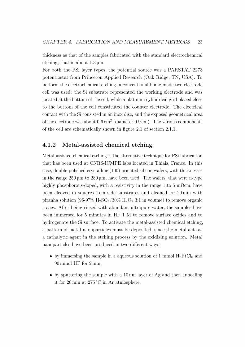
Metal-assisted chemical etching is the alternative technique for PSi fabricationthat has been used at CNRS-ICMPE labs located in Thiais, France. In thiscase, double-polished crystalline (100)-oriented silicon wafers, with thicknessesin the range 250 µm to 280 µm, have been used. The wafers, that were n-typehighly phosphorous-doped, with a resistivity in the range 1 to 5 mWcm, havebeen cleaved in squares 1 cm side substrates and cleaned for 20min withpiranha solution (96-97% H2SO4/30% H2O2 3:1 in volume) to remove organictraces. After being rinsed with abundant ultrapure water, the samples havebeen immersed for 5 minutes in HF 1 M to remove surface oxides and tohydrogenate the Si surface. To activate the metal-assisted chemical etching,a pattern of metal nanoparticles must be deposited, since the metal acts asa cathalytic agent in the etching process by the oxidizing solution. Metalnanoparticles have been produced in two different ways:
• by immersing the sample in a aqueous solution of 1 mmol H2PtCl6 and90mmol HF for 2min;
• by sputtering the sample with a 10 nm layer of Ag and then annealingit for 20min at 275 �C in Ar atmosphere.

CHAPTER 4. FABRICATION AND MEASUREMENT METHODS 24
The etching has been performed just after the metallization by immersingthe samples for 20min in an HF/H2O2 aqueous solution, where [HF]=1,21 Mand [H2O2]=0,21 M, so setting a ratio:
⇢ =[HF ]
[HF ] + [H2O2](4.1)
of 0,75 for all the etching procedures.
4.2 Impregnation of the substrates
All the impregnations of PSi matrices have been carried out at the PoroSiLab.Different materials have been used to impregnate the samples: the chemicalfilling of the pores with melanin is described in 4.2.1, while the electrochemicalimpregnation processes with erbium and nickel are treated in 4.2.2 and 4.2.3,respectively.
4.2.1 Porous silicon filling with melanin
Polymerization of melanin inside the samples pores was carried out usingAmmonia-Induced Solid State Polymerization (AISSP) procedure reportedin [103]. The impregnation starts by dissolving a given amount of DHImonomer in a given volume of EtOH. In this dissertation, the effect of severalconcentrations has been explored: 8, 16 and 24 mgmL�1. Then, a drop ofthe monomer solution is deposited on the sample and distributed uniformlyon the porous top surface by spin coating for 3 minutes. This has the doubleeffect of favoring the penetration of the DHI solution within the pores andof forming a homogenous thin organic layer on the top of the sample. Onceimpregnated, the samples were exposed to NH3 atmosphere for the AISSPoxidation of the molecules and therefore for the polymerization of DHI. Theduration of this process was 15 minutes.

CHAPTER 4. FABRICATION AND MEASUREMENT METHODS 25
4.2.2 Porous silicon doping with erbium
PSi samples were electrochemically doped with erbium using an ethanoic0.11M solution of Er(NO3)3 5 H2O salt. Before the beginning of the process,the samples were let in contact with the solution for one minute under slowstirring, in order to facilitate the solution exchange at the external surface ofthe PSi layer. The electrochemical doping was carried out in constant currentmode, applying 1mA for different times, depending on the amount of erbiumit was supposed to deposit in the PSi matrix. The chosen doping times were30, 100, 150, 200, 250 and 300 s, corresponding to Er amounts of 1.2, 4.0, 6.0,8.0, 10.0, 12.0 %, respectively. Since there is always a gradient in the erbiumcontent inside the porous matrixes, these values refer to the content towardsthe external surface. Once the electrochemical impregnation is finished, thecell must be immediately empty in order to prevent the Er-ions to go back tothe bulk solution; then, after removing the sample from the cell, it must becarefully and quickly rinsed with distilled water, again to avoid the removalof the erbium from the pores.
4.2.3 Porous silicon filling with nickel
The electrochemical filling of PSi with nickel has been performed using the so-called "Watts bath" containing NiCl2 45 g L�1, NiSO4 300 g L�1 and H3BO4
45 g L�1. To achieve an optimal filling of the pores, the electrochemical Nideposition process was performed by pulsed electrodeposition: current densitypulses at �1.6mAcm�2 were applied for 5 s separated by a 5 s delay at zerocurrent for 120 cycles.
4.3 Structural characterization
Structural and chemical characterization of the samples have been done inresearch centers other than University of Cagliari. In particular, SEM andSEM-EDS analysis on Er-doped PSi samples have been carried out at KAUSTthanks to the collaboration with the group of A. Falqui, while the same kind
CHAPTER 4. FABRICATION AND MEASUREMENT METHODS 26
of analysis on MACE nanostructured PSi filled with melanin has been doneat CNRS-ICMPE (Paris) by the group of S. Bastide; the structural analysisof ENL samples, both in plane view and in cross section, have been performedwith the SEM at INRIM by the group of L. Boarino. All the details aboutSEM analysis are reported in section 4.3.1. Both Er-doped and Ni-filledPSi samples have been analyzed by tomography at Minatec of Grenoble, asreported in 4.3.2.
4.3.1 SEM
Er-doped PSi samples were analyzed by using a Zeiss Merlin scanning electronmicroscope, equipped with a Schottky field emission gun, a Raith patterngenerator, an Oxford EDS X-Max SDD detector with an area of 80mm2 andthe AzTecEnergy EDS analysis software. To collect both the EDS elementalmaps and spectra, the microscope operated at an acceleration voltage of 15 kVand a beam current of 5.5 nA. EDS quantitative analysis was performed byusing a ZAF standardless method. The X-Ray peaks chosen for both theEDS mapping and quantitative analysis were the O K, Si K and the Er L,respectively. The same microscope has been used to collect SEM image ofthe samples surface and that of the PSi layers in cross sectional view, usingthe secondary electron (SE) signal. In this case, the microscope accelerationvoltage was 4 kV and the beam current 300 pA. SEM images and SEM-EDSanalysis of MACE samples filled with melanin were obtained with a MerlinFEG microscope from Zeiss, equipped with AZtec systems (EDS Advanced,HKL Advanced Nordlys Nano, Oxford Instruments). The morphologicalcharacterization of ENL samples was carried out using a Field Emission GunSEM (FEI Inspect F).
4.3.2 Electron tomography
ET analysis have been carried on PSi with erbium as a collection of a seriesof scanning transmission electron microscopy (STEM) images. In particular,needles with a diameter of few hundreds nanometers have been extractedby the samples using a focused ion beam (FIB) FEI Strata instrument.

CHAPTER 4. FABRICATION AND MEASUREMENT METHODS 27
The extraction from the sample has been performed after being protectedwith a layer of tetraethyl orthosilicate, glued at the top of a tip and finallyinserted in the transmission electron microscope (TEM). The acquisitionshave been performed either on a FEI Titan Ultimate TEM or on a FEI ThemisTEM, working in scanning mode (STEM) with a high angle annular darkfield (HAADF) detector, in order to both prevent from the diffraction thatcould limit the reliability of the sample volume reconstruction and enhancethe contrast due to the atomic number difference between Si and Er. Theacceleration voltage during the acquisition was 80 kV to limit the damageto the PSi structure. During the acquisition, the samples were tilted overa 180° tilt range, with a constant tilt step of 1°. The 181 acquired images(projections) have been analyzed with a dedicated algorithm to reconstructthe needle volume, after a fine alignment between the needle projectionsand the tilt axis, according to the procedure reported in [104]. Moreover, anon-rigid alignment has been used to correct the possible sample deformationthat may occur during the needle tomography series acquisition and maylead to deformation-related artifacts during the 3D-reconstruction [105]. AMatlab-based custom-made software has been used for projection denoising,alignment and reconstruction of the samples volume.
4.4 Samples measurements
4.4.1 Photocurrent measurements
Photocurrent measurements on PSi samples with melanin were carried out toevaluate the device properties. In order to perform these measurements, ametallic contact was prior deposited on the samples top surface: in particular,a semitransparent gold layer was sputtered with an Emitech K450 on a portionof the impregnated surface, concentrically; the back contact, was obtainedwith a little drop of silver paste directly on the bulk silicon, previouslyscratched in order to remove the native oxide layer. To illuminate the samples,a white light source (tungsten halogen lamp) was focused on the samplessurface by means of an optical fiber and of a microscope objective to a circular

CHAPTER 4. FABRICATION AND MEASUREMENT METHODS 28
area with a diameter of 0.4 cm. Both dark and white light photocurrentmeasurements have been done, and a series of long-pass filters was used toobserve the spectral response in the UV-Vis range (305 nm to 830 nm). Themeasurement of the produced photocurrent was done using either a Keithley(Keithley Instruments, Cleveland, OH, USA) 6487 or 2450 SMU multimeteraccording to the experimental needs.
4.4.2 Photoluminescence measurements
Continuous-wave photoluminescence
PL measurements on Er-doped PSi samples have been carried out at roomtemperature in continuous wave mode. A diode-pump solid-state laser, withan excitation wavelength of 532 nm, an excitation power of 770mW and aspot size of about 200 µm has been used. The optical emission from thesamples was dispersed by a 30 cm focal length Acton spectrometer, equippedwith a 75 groves/mm grating blazed at 1200 nm; the detector was an InGaAsAndor line CCD.
Time-resolved photoluminescence
Time-resolved PL measurements on the same kind of samples, instead,have been done employing a pulsed regenerative amplifier as light source(Quantronix Integra, 100 fs pulse duration, 1 kHz repetition rate, 1mJ ener-gy/pulse, 800 nm in wavelength). For the detection, the same spectrometerused for continuous wave measurements has been used, but the light wasdirected to a second output port equipped with a Hamamatsu InGaAs fastphotomultiplier, used in current mode and whose signal detected with aTektronix GHz oscilloscope.
Spatially-resolved photoluminescence
Micro-PL measurements and mappings were done at room temperature usinga Horiba LabRAM HR spectrometer. A laser of 2mW power and 633 nm
wavelength was focused with a 100x Leica objective (numerical aperture0.9). The spectrometer was equipped with a 150 grooves/mm grating andan InGaAs array. Due to long acquisition times, a background spectrum was

CHAPTER 4. FABRICATION AND MEASUREMENT METHODS 29
systematically subtracted.

Part III
Results and discussion
30

Chapter 5
Porous silicon impregnated with
melanin
In this chapter, the results obtained on a hybrid heterojunction between PSiand eumelanin are presented. In particular, we will describe in 5.1 the adoptedstrategies to improve the interface stability between eumelanin and PSi in10 nm-diameter PSi samples. Section 5.3 is dedicated to the enhancementof the junction stability that has been obtained thanks to the introductionof a new method of PSi fabrication, whose pores diameter is about 50 nm.Finally, in section 5.4 is reported the attempt to produce a similar hybridheterojunction using eumelanin to fill nanostructured porous silicon obtainedby MACE.
5.1 Thin-pores samples with eumelanin
This hybrid heterojunction with photovoltaic properties has been proposedin 2012 by Mula et al. [106] using n-type PSi and eumelanin. The latter isa natural pigment characterized by a relatively high proton-based electricalconductivity [54] and a dark colour, and it behaves like a p-type semiconductor;for those reasons, a p-n junction can be produced if eumelanin is insertedinto the n-type PSi. An increase of the optical absorption range with respectto Si and to the bare PSi has been found after the insertion of the organic
31
CHAPTER 5. POROUS SILICON IMPREGNATED WITH MELANIN32
1.0
0.8
0.6
0.4
0.2Nor
mal
ized
pho
tocu
rren
t
800700600500400Cutoff wavelength (nm)
Porous silicon with DHI
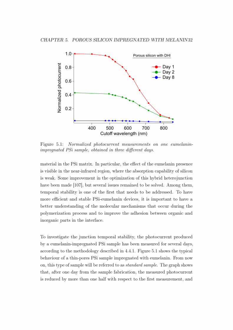
Day 1 Day 2 Day 8
Figure 5.1: Normalized photocurrent measurements on one eumelanin-impregnated PSi sample, obtained in three different days.
material in the PSi matrix. In particular, the effect of the eumelanin presenceis visible in the near-infrared region, where the absorption capability of siliconis weak. Some improvement in the optimization of this hybrid heterojunctionhave been made [107], but several issues remained to be solved. Among them,temporal stability is one of the first that needs to be addressed. To havemore efficient and stable PSi-eumelanin devices, it is important to have abetter understanding of the molecular mechanisms that occur during thepolymerization process and to improve the adhesion between organic andinorganic parts in the interface.
To investigate the junction temporal stability, the photocurrent producedby a eumelanin-impregnated PSi sample has been measured for several days,according to the methodology described in 4.4.1. Figure 5.1 shows the typicalbehaviour of a thin-pores PSi sample impregnated with eumelanin. From nowon, this type of sample will be referred to as standard sample. The graph showsthat, after one day from the sample fabrication, the measured photocurrentis reduced by more than one half with respect to the first measurement, and

CHAPTER 5. POROUS SILICON IMPREGNATED WITH MELANIN33
it is around zero after one week. The possible explanations for this behaviourcould be likely linked to phenomena taking place during the polymerization,the organic/inorganic interface formation and/or within the polymer itselfonce the polymerization process is finished. These can affect both the polymerconductivity and the Si/polymer interface resistance. In order to achievea better understanding of the mechanisms involved in the hybrid materialfabrication steps and to improve the junction durability, we investigated thePSi/eumelanin interface and the polymerization process. The insufficientformation of stable chemical bonds between PSi and eumelanin can lead tothe formation of an unstable interface; in fact, a typical phenomenon thathappens during polymerization is the volume contraction with respect to thevolume occupied by the initial monomers. This is a general problem that canhas relevant consequences for the applications involved, for example in case oforthodontic resin [108]. In this eventuality, a partial detachment between theorganic and inorganic parts of the junction could occur, leading to a reductionof photocurrent generation. To investigate what parameter was more relevantin the interface formation and lifetime, we modified several parameters,namely the amount of SiO2 at the interface, the monomer distribution inthe impregnation solution and finally the average pore diameter. This latteraspect required a dedicated study for an optimal fabrication process and willbe described in paragraph 5.2. The first step was a light electrochemicaloxidation of the porous inner surface, since the presence of SiO2 is expectedto favour the chemical bond of DHI to the surface thanks to a better affinityof the organic monomer with silica. It is reported in literature that a thinoxide layer can enhance the photovoltaic properties in hybrid silicon/organicdevices [109–113]. This oxidation has to be carefully calibrated since, if inexcess, it would block the charge transfer between the two materials, cancelingthe photovoltaic behaviour. Since the electrochemical oxidation process ismainly governed by the transferred charge, we chose a constant currentapproach using a �2mA current and a 0.1 M KNO3 ethanoic solution. Theoxidation grade was calculated as follows: an oxidation of 50 at% (measuredby SEM-EDS) is obtained in a constant current process for a process durationcorresponding to the time needed to reach the maximum applied voltage of

CHAPTER 5. POROUS SILICON IMPREGNATED WITH MELANIN34
1.0
0.8
0.6
0.4
0.2Nor
mal
ized
pho
tocu
rren
t
800700600500400Cutoff wavelength (nm)
Day 1 Day 2 Day 8
Slightly oxidized PSi with DHI
Figure 5.2: Normalized photocurrent measurements on one slightly oxidizedeumelanin-impregnated PSi sample, obtained in three different days. Theoxidation of the PSi matrix has been done electrochemically before the impreg-nation with eumelanin.
the available potentiostat (10V). Using this reference, the oxidation of theinner PSi samples in this case was about 3%; direct measurement of the oxidethickness on the pore walls has not been done because, given the complexstructure of the pores, it is a result hard to achieve even with state-of-the-arttechniques and beyond the scope of this research. In figure 5.2 we reportthe typical behaviour of a hybrid sample where a slight oxidation has beenperformed before the impregnation. A small improvement in the junctionstability is visible: in the first two days the photocurrent drops by 40%, whileit was 60% in the case of the standard samples. Moreover, one week after thesample fabrication, photocurrent was still 15% of the initial value, while inthe previous case the photocurrent values after one week were almost zero.This result implies that while the interface clearly plays a role and is affectedby the chemical details during the fabrication process, it does not seems tobe the key parameter in our methodology.
The second approach used to improve the temporal stability was based on

CHAPTER 5. POROUS SILICON IMPREGNATED WITH MELANIN35
1.0
0.8
0.6
0.4
0.2
0.0
Nor
mal
ized
pho
tocu
rrent
800700600500400Cutoff wavelength (nm)
(b)
Day 1 Day 2 Day 8
Non-oxidized PSi with DHI+DHICA
Figure 5.3: Normalized photocurrent measurements on one PSi sample filledwith a mixed solution of DHI and DHICA, obtained in three different days.
the modification of the organic part of the junction. In particular, a solutioncontaining DHI and DHICA in equal parts was used to impregnate the PSimatrices. The reason at the base of this choice was once again to improve thechemical bonds between the two parts of the hybrid junction. Since DHICAhas a molecule similar to DHI but with a carboxylic group –COOH, thisadditional part can act as an anchor with the porous walls through oxygenbridges, as it happens in other hybrid photovoltaic systems [114]. The typicalbehaviour of the samples impregnated with the DHI/DHICA mix is presentedin figure 5.3.
Despite the expectations, the addition of DHICA to the monomer solutionsdid not lead to a stabilization of the junction. The only difference with respectto the case of the standard sample was the slight improvement in long termphotocurrent values: after eight days from the sample realization, it waspossible to measure low but not zero photocurrent, as was the case of oxidizedsamples (figure 5.2). Once again, even if the parameter we modified shows

CHAPTER 5. POROUS SILICON IMPREGNATED WITH MELANIN36
4
3
2
1
0
Abso
rban
ce
800700600500400300Wavelength (nm)
0.5mg DHI in 1mL EtOH
Absorbance spectra recorded every 30' from 0 to 420'
Figure 5.4: Absorbance spectra evolution of a solution made with 0.5mg ofDHI dissolved in 1mL EtOH.
some positive effect on the improvement of the junction photovoltaic lifetime,it still does not give a strong indication of being a key parameter.
Since the two parameters we checked did not give satisfactory results interms of lifetime improvement, it was evident that we needed to resort toa wider strategy to solve the issue. We therefore decided to investigate thepolymerization process using a combined experimental and computationalapproach. This part has been done in collaboration with two computationalgroups of the Physics Department of the University of Cagliari: the team ofG. Cappellini contributed to the understanding of melanin optical properties,while L. Colombo’s group studied its electronic and structural characteristics.Polymerization of DHI is still a matter of debate and many research groupsare working on deciphering the chemical structure of the eumelanin moleculethat is formed during polymerization [115–120]. In the optic to shed lighton the DHI polymerization process, the evolution of the absorbance spectraof an air-equilibrated solution of DHI in EtOH was measured and comparedwith the absorbance simulated spectra of several tetramers that literaturereports as the most probable models for the polymerization of DHI.
In particular, the absorbance of three different concentrated solutions wasstudied:

CHAPTER 5. POROUS SILICON IMPREGNATED WITH MELANIN37
• 0.25mg DHI dissolved in 1mL of EtOH
• 0.50mg DHI dissolved in 1mL of EtOH
• 1.00mg DHI dissolved in 1mL of EtOH
and the spectra were recorded every 30min from the preparation of the solutionto 420min, except from the third one that was studied for 360min because theabsorption was very strong from the beginning and made impossible to recordabsorption spectra for delays longer than 360 min. Since the evolution of theabsorbance spectra was the same for all the different concentrations, it hasbeen decided to report here only the absorption spectra of the 0.5mgmL�1
concentrated solution, because it has the best signal-to-noise ratio (figure 5.4).In order to emphasize the absorbance evolution of the different peaks, theabsorbance variation at three different wavelengths was studied (figure 5.5):
• 330 nm, that is the position of a shoulder in the UV range;
• 460 nm, that is the position of the most visible peak;
• 780 nm, that is the position of the broad peak in the NIR range.
In particular, in figure 5.5 (a) the absorbance variation with respect to itsinitial value at the given wavelength and normalized with respect to themaximum increase for each curve is reported; in figure 5.5 (b) is shown theabsorbance increase in each step, normalized with respect to the maximumpositive value for each curve. From the analysis it is clear that the peaks atdifferent wavelengths have different behaviours: the band at 330 nm increasesfaster than the other two, and the peak at 780 nm reaches its maximum andstarts to decrease while other bands are still increasing. Moreover, if thepeaks at 330 nm and 780 nm reach their maximum approximately at the sametime, the peak at 460 nm reaches its maximum a little later. This evolutioncan be associated to the polymerization process of the DHI that is occurringin the ethanoic solution.To better understand these results, it is useful to make a comparison with whatis reported on reference [120] about DHI polymerization in aqueous buffer:

CHAPTER 5. POROUS SILICON IMPREGNATED WITH MELANIN38
1.0
0.8
0.6
0.4
0.2
0.0
Norm
aliz
ed a
bsor
banc
e
4003002001000Time (min)
λ = 330nm λ = 460nm λ = 780nm
DHI 0.5mg/mL
(a)
1.0
0.8
0.6
0.4
0.2
0.0
-0.2
Norm
aliz
ed a
bsor
ptio
n va
riatio
n
4003002001000Time (min)
λ = 330nm λ = 460nm λ = 780nm
DHI 0.5mg/mL
(b)
Figure 5.5: Analysis of the absorbance evolution for three different significantwavelengths. (a) Normalized absorbance evolution. (b) Absorbance increaseevery 30min, normalized to the maximum positive value for each curve.
under such condition, during the polymerization of DHI there is the formationof broadly visible chromophores at around 560 nm, that was attributed to amixture of dimers or higher level oligomers. In the same way, it is possible tosay that the three bands shown in the experiments reported herein correspondto the formation of dimers or oligomers from the DHI monomers. Then,we can conclude that DHI polymerizes also in an air-equilibrated organicmedium and that there is the formation of some more defined chromophoricspecies with respect to the same process in an aqueous medium. It could bepossible that the species that absorbs at 780 nm is an unstable precursor ofthe one that absorbs at 460 nm, but no further experiments have been doneto demonstrate this hypothesis. The fact that the main chromophore persistsmore in ethanol than in water could be related to the stronger solvation effectsin organic solvents, which limits the aggregation and precipitation of darkmaterial.
The experimental results have been compared with tetramer models that havebeen taken from literature as the possible molecules that form during thepolymerization of DHI. Actually, the possible variety of isomers that populateeach oligomer level is extremely wide [54,57,121,122], and they can also differ intheir redox state. This means that, for each DHI monomer unit, it can exist thecatechol form as well as the 2-electrons oxidation state (5,6– indolequinone, IQ)and its tautomers, the quinoneimine (QI) and the quinonemethide (QM) [123].The structural variety of the molecules contributes to the molecular disorder of

CHAPTER 5. POROUS SILICON IMPREGNATED WITH MELANIN39
NH
HO
HO5,6-dihydroxyindole(DHI)
[O]
NH
HO
HO
model tetramer
NH
OH
OH
dimerization(2,4'-coupling)
DHI
DHI
OHHO
HN
NH
HO
HO
OHHO
HN
NH
OH
OH
NH
HO
HO
OHHO
HN
OHHO
HN
2,4'-coupling
24'
2
4'24'
Figure 5.6: Polymerization scheme where the oxidative coupling of DHI leadsto isolated 2,4’ dimer and 2,4’:2’,4” trimer and model tetramer (Model 1) [60].
eumelanin, while the different oxidation levels of each molecule contribute toits electronic disorder. Since disorder from both molecular and electronic origincontribute to the overall properties of eumelanin, disorder control is a goodapproach to gain control over the eumelanin polymerization process [122].The model tetramer used for the computational part of this research is2,4’:2’,4":2",4’"-tetraindolyl (Model 1) and the polymerization path thatbrings to that model is reported in figure 5.6.
According to this scheme, the formation of the final tetramer is the result ofthe progressive coupling of a DHI monomer with the 2,4’-dimer, obtained by

CHAPTER 5. POROUS SILICON IMPREGNATED WITH MELANIN40
Figure 5.7: Different oxidation states of the model tetramer called Model 1.The characteristics are the following: Model 1-a (2-electron oxidation, 1 C=Ogroup); Model 1-b (2-electron oxidation, 2 C=O groups); Model 1-c (6-electronoxidation, 4 C=O groups); Model 1-d (8-electron oxidation, 6 C=O groups).
the oxidation of the monomer, and then with the 2,4’:2’,4"-terindolyl trimer.Among the possible tetramers proposed in literature for eumelanin buildingblock, it has been chosen Model 1 as the result of a compromise betweenthe need for a sufficient level of molecular complexity and the computationalcosts associated with higher oligomers. Moreover, the absence of specificsymmetry properties and its origin from major isolated DHI-based oligomershave been considered to make this choice. Density-Functional Theory, usingthe plane-wave Quantum Expresso package with the PBE (Perdew, Burkeand Ernzerhof, [124, 125]) exchange correlation function, has been used byL. Colombo’s group to investigate the formation and stacking energies ofModel 1 as a function of its oxidative states (figure 5.7). The four differentoxidation states correspond to two tautomers of the putative two-electronoxidation product, one tautomer for the six-electron oxidation product andone tautomer for the eight-electron oxidation product.
The formation energies and the stacking energies of all the four moleculeshave been calculated in vacuum and for two different solvents, where thechoice of methanol as a solvent was guided by the need to be closer to theexperimental condition of dissolving DHI in ethanol. The results are reportedin table 5.1.
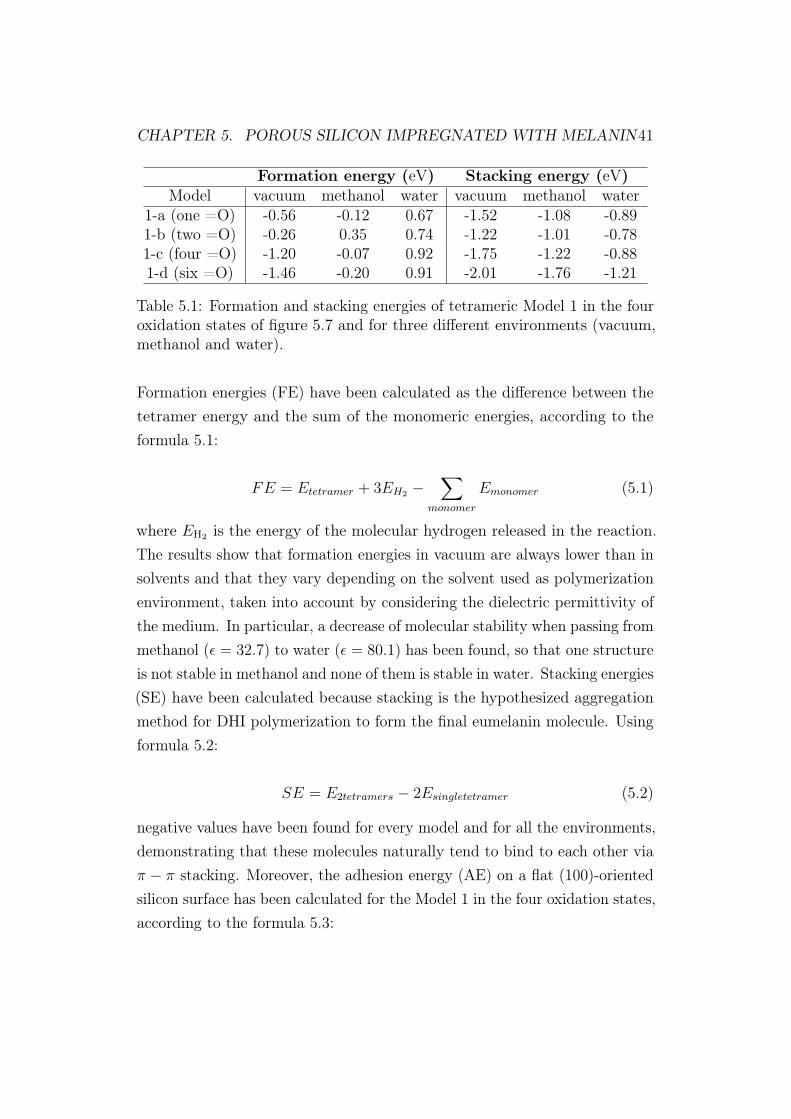
CHAPTER 5. POROUS SILICON IMPREGNATED WITH MELANIN41
Formation energy (eV) Stacking energy (eV)
Model vacuum methanol water vacuum methanol water1-a (one =O) -0.56 -0.12 0.67 -1.52 -1.08 -0.891-b (two =O) -0.26 0.35 0.74 -1.22 -1.01 -0.781-c (four =O) -1.20 -0.07 0.92 -1.75 -1.22 -0.881-d (six =O) -1.46 -0.20 0.91 -2.01 -1.76 -1.21
Table 5.1: Formation and stacking energies of tetrameric Model 1 in the fouroxidation states of figure 5.7 and for three different environments (vacuum,methanol and water).
Formation energies (FE) have been calculated as the difference between thetetramer energy and the sum of the monomeric energies, according to theformula 5.1:
FE = Etetramer + 3EH2 �X
monomer
Emonomer (5.1)
where EH2 is the energy of the molecular hydrogen released in the reaction.The results show that formation energies in vacuum are always lower than insolvents and that they vary depending on the solvent used as polymerizationenvironment, taken into account by considering the dielectric permittivity ofthe medium. In particular, a decrease of molecular stability when passing frommethanol (✏ = 32.7) to water (✏ = 80.1) has been found, so that one structureis not stable in methanol and none of them is stable in water. Stacking energies(SE) have been calculated because stacking is the hypothesized aggregationmethod for DHI polymerization to form the final eumelanin molecule. Usingformula 5.2:
SE = E2tetramers � 2Esingletetramer (5.2)
negative values have been found for every model and for all the environments,demonstrating that these molecules naturally tend to bind to each other via⇡ � ⇡ stacking. Moreover, the adhesion energy (AE) on a flat (100)-orientedsilicon surface has been calculated for the Model 1 in the four oxidation states,according to the formula 5.3:

CHAPTER 5. POROUS SILICON IMPREGNATED WITH MELANIN42
AE = Esystem �X
components
Ecomponents (5.3)
where Esystem and Ecomponents are the energy of the composite system andthe energy of the single components (non-interacting surface and molecule),respectively. The results are reported in table 5.2 and, once again, the higheris the number of C=O groups, the stronger is the adhesion between themolecule and the Si surface, probably because there are a more efficient⇡-electron overlap and a greater polarization by resonance effects.
Adhesion energy (eV)
Model 1-a (one C=O) -5.37Model 1-b (two C=O) -6.73Model 1-c (four C=O) -7.85Model 1-d (six C=O) -10.99
Table 5.2: Adhesion energies of tetrameric Model 1 in the four electronicconfigurations of figure 5.7.
Since for Model 1-d the lower stacking energy has been obtained, it means thatthe higher is the oxidation state of the molecule the higher is the probability ofstacking during the polymerization process, at least among the oligomers thathave been analyzed in this research. For this reason, Model 1-d has been alsoused to calculate the absorption spectra to be compared with the experimentalcurve and to understand if structures related to the model tetramer maybe responsible for the optical behaviour of DHI oxidation reported in figure5.4. The comparison between the experimental absorption data for DHIpolymerization in EtOH and the calculated one for Model 1-d is presented infigure 5.8.
Even if at first sight the appearance is strongly different, some commonfeatures must be evidenced. Unfortunately, the maximum peak found forModel 1-d does not correspond to a maximum in the experimental absorption,but the affinities are several. First of all, Model 1 exhibits three peaks atvery close wavelengths to the three peaks previously taken into account for
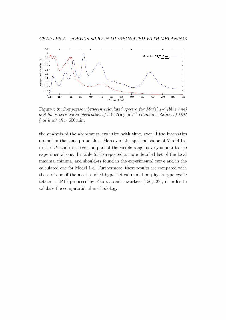
CHAPTER 5. POROUS SILICON IMPREGNATED WITH MELANIN43
Model 1-d
Figure 5.8: Comparison between calculated spectra for Model 1-d (blue line)and the experimental absorption of a 0.25mgmL�1 ethanoic solution of DHI(red line) after 600min.
the analysis of the absorbance evolution with time, even if the intensitiesare not in the same proportion. Moreover, the spectral shape of Model 1-din the UV and in the central part of the visible range is very similar to theexperimental one. In table 5.3 is reported a more detailed list of the localmaxima, minima, and shoulders found in the experimental curve and in thecalculated one for Model 1-d. Furthermore, these results are compared withthose of one of the most studied hypothetical model porphyrin-type cyclictetramer (PT) proposed by Kaxiras and coworkers [126, 127], in order tovalidate the computational methodology.
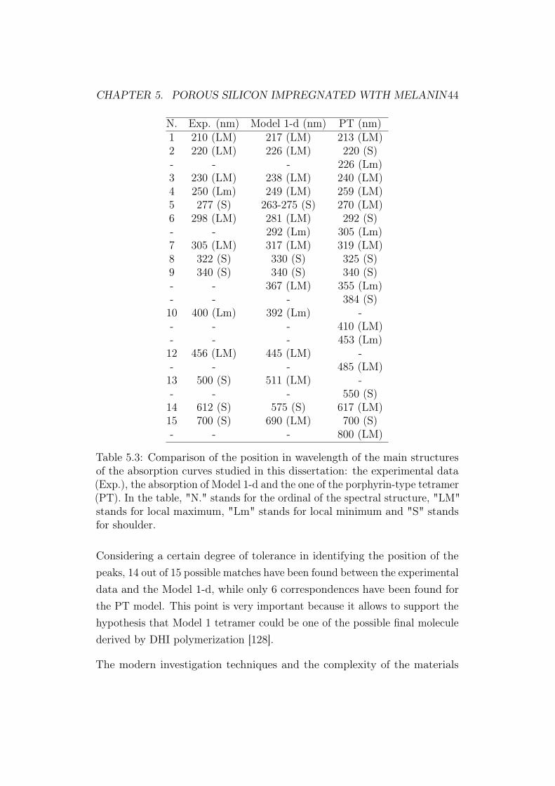
CHAPTER 5. POROUS SILICON IMPREGNATED WITH MELANIN44
N. Exp. (nm) Model 1-d (nm) PT (nm)1 210 (LM) 217 (LM) 213 (LM)2 220 (LM) 226 (LM) 220 (S)- - - 226 (Lm)3 230 (LM) 238 (LM) 240 (LM)4 250 (Lm) 249 (LM) 259 (LM)5 277 (S) 263-275 (S) 270 (LM)6 298 (LM) 281 (LM) 292 (S)- - 292 (Lm) 305 (Lm)7 305 (LM) 317 (LM) 319 (LM)8 322 (S) 330 (S) 325 (S)9 340 (S) 340 (S) 340 (S)- - 367 (LM) 355 (Lm)- - - 384 (S)
10 400 (Lm) 392 (Lm) -- - - 410 (LM)- - - 453 (Lm)
12 456 (LM) 445 (LM) -- - - 485 (LM)
13 500 (S) 511 (LM) -- - - 550 (S)
14 612 (S) 575 (S) 617 (LM)15 700 (S) 690 (LM) 700 (S)- - - 800 (LM)
Table 5.3: Comparison of the position in wavelength of the main structuresof the absorption curves studied in this dissertation: the experimental data(Exp.), the absorption of Model 1-d and the one of the porphyrin-type tetramer(PT). In the table, "N." stands for the ordinal of the spectral structure, "LM"stands for local maximum, "Lm" stands for local minimum and "S" standsfor shoulder.
Considering a certain degree of tolerance in identifying the position of thepeaks, 14 out of 15 possible matches have been found between the experimentaldata and the Model 1-d, while only 6 correspondences have been found forthe PT model. This point is very important because it allows to support thehypothesis that Model 1 tetramer could be one of the possible final moleculederived by DHI polymerization [128].
The modern investigation techniques and the complexity of the materials

CHAPTER 5. POROUS SILICON IMPREGNATED WITH MELANIN45
involved do not allow to look more deeply at the interface of the PSi-melaninheterojunction. To make up for the absence of experimental techniques, thepolymer behaviour at the interface with a Si surface has been studied witha computational approach by our collaborator of L. Colombo’s group of theUniversity of Cagliari. The aim of the computational study was to elucidatehow the interface affects polymer structural features, reaching an atomicresolution that is hardly obtainable in experiments. The computationaltechnique that has been adopted is the model potential molecular dynamics(MPDP), since it allows the analysis of the adhesion of eumelanin on silicon,building a realistic system of tens of nanometers. Starting from the resultsobtained in the analysis of the process of formation and adhesion of a singletetrameric molecule on silicon with different oxidation states reported above,the following study is focused on the two tetrameric protomolecules with thebest formation and adhesion energies. The two molecules, shown in figure5.9 and mentioned hereafter as model 1 (left side of Figure 5.9) and model 2(right side of Figure 5.9), are respectively the experimentally characterizedmolecule from Panzella et al. [128] and the structure from Kaxiras et al. [126].The model 2 has never been isolated experimentally, but it has been usedhere as a representative example of a possible flat oligomer in the eumelaninpolymer, as opposed to the linear and more flexible model 1.
The analyzed physical system was formed by a silicon (100) 25 × 25 substrateand a number of 5400 protomolecules of either model 1 or model 2. Theatoms were 311 600 in total for each sample. At first, the molecules wererandomly placed in a region above the substrate and then let them movetoward it with an initial velocity of 0.001Å fs�1. The system was then letto evolve for 106 time-steps until all the molecules were deposited. Finally,a further 106 time-steps constant-temperature run was performed in orderto estimate the system stability at finite temperature. During this last step,the density profile and root-mean-square displacement were sampled. Thismulti-step approach is intended to reproduce the experimental spin coatingprocedure used to generate uniform hybrid films [129], that we used also inthis dissertation (section 4.2.1). The substrate temperature was kept at room
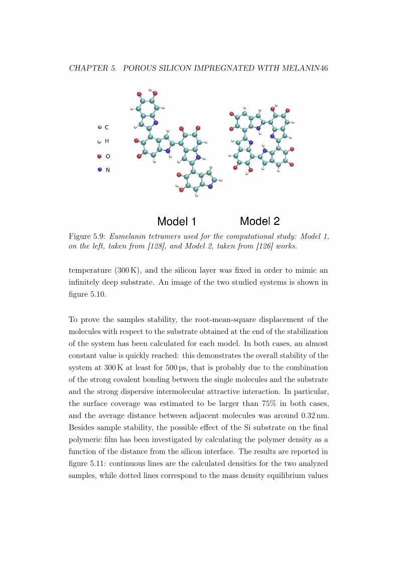
CHAPTER 5. POROUS SILICON IMPREGNATED WITH MELANIN46
Figure 5.9: Eumelanin tetramers used for the computational study: Model 1,on the left, taken from [128], and Model 2, taken from [126] works.
temperature (300K), and the silicon layer was fixed in order to mimic aninfinitely deep substrate. An image of the two studied systems is shown infigure 5.10.
To prove the samples stability, the root-mean-square displacement of themolecules with respect to the substrate obtained at the end of the stabilizationof the system has been calculated for each model. In both cases, an almostconstant value is quickly reached: this demonstrates the overall stability of thesystem at 300K at least for 500 ps, that is probably due to the combinationof the strong covalent bonding between the single molecules and the substrateand the strong dispersive intermolecular attractive interaction. In particular,the surface coverage was estimated to be larger than 75% in both cases,and the average distance between adjacent molecules was around 0.32 nm.Besides sample stability, the possible effect of the Si substrate on the finalpolymeric film has been investigated by calculating the polymer density as afunction of the distance from the silicon interface. The results are reported infigure 5.11: continuous lines are the calculated densities for the two analyzedsamples, while dotted lines correspond to the mass density equilibrium values

CHAPTER 5. POROUS SILICON IMPREGNATED WITH MELANIN47
Figure 5.10: Schematic representation of the eumelanin-silicon interfaceformed upon the deposition process described in the text.

CHAPTER 5. POROUS SILICON IMPREGNATED WITH MELANIN48
Figure 5.11: Time evolution of the root-mean-square displacements for thetwo models considered (left-side); polymer mass density profile as a functionof the distance perpendicular to the interface where z < 1.2nm correspondsto the silicon substrate (right-side).
without the substrate. From the graph it is visible that polymer densityincreases dramatically for z < 1.3 nm, which is close to the silicon substrate:it is probably due to the strong interaction between molecule and substrate.For 1.3 nm < z < 5 nm, the density is generally larger than bulk, and thismeans that the presence of the silicon substrate unavoidably affects the localproperties of the polymeric film in a non-negligible spatial region as large as4-5 nm beyond the interface.
The pores of the standard samples have an average diameter in the range10-15 nm; according to the computational results shown in figure 5.11, then,the majority of the polymer volume inside the pore is strongly affected bythe silicon interface. The comparison of the computational results with thecharacteristics of our samples is important to find a possible explanationfor the fast degradation that we showed above in terms of photocurrentproduction. This phenomenon could have origin in the polymerization ofDHI inside the pores. It is known that, during the polymerization process,there is the production of hydrogen peroxide [130, 131]; unfortunately, theH2O2 is a strong oxidant for the Si surface, so it gradually transforms thepores inner surface in an insulating layer, decreasing and eventually stoppingthe photocurrent generation. Differences in the polymer density may affect

CHAPTER 5. POROUS SILICON IMPREGNATED WITH MELANIN49
Thin pore Large pore40-60 nm10-15nm
Unmodified polymer(larger intermolecular distance)
Interface-affected polymer(reduced intermolecular distance)
Interface thickness: about 5nm
Easy H2O2 diffusion towards PSi interface
Difficult H2O2 diffusion towards PSi interface
Figure 5.12: Scheme of the different eumelanin structures within the siliconpores depending on the pores diameter.
the H2O2 diffusion inside the pores during the polymerization process. Ifconsidering our standard samples, whose pores are quite thin, it could be thatthe hydrogen peroxide molecules diffuse quickly toward the interface betweensilicon and eumelanin. As a consequence, the oxidation of the silicon walls isfast and we observe it as a rapid degradation of the photocurrent properties.On the contrary, we can hypothesize that a significative increase of the poresdiameter should modify the polymer behaviour. A schematic of the proposedinterpretation of the polymer behaviour is shown in figure 5.12. For sampleswith larger pores, in fact, the diffusion of the H2O2 molecules toward theorganic/inorganic interface may be slower, because they tend more to staywhere the polymer density is lower. As a consequence, the oxidation of thesilicon walls and the consequent degradation of the photovoltaic properties ofthe sample would be slower.

CHAPTER 5. POROUS SILICON IMPREGNATED WITH MELANIN50
5.2 Electrochemical Nanolithography for larger
pores fabrication
To verify the assumption that pores diameter would affect the polymerbehaviour, we fabricated PSi samples with larger pores, and repeated thestudy on the stability of the samples impregnated with melanin made withthin-pores samples. Moreover, a porous structure with larger pores shouldimprove the mobility of the solution and could help to improve the poresimpregnation with the organic material. However, obtaining porous siliconsamples with larger pores is not trivial, since pores diameter depends on theelectrochemical parameters, like anodic etching current and HF concentrationof the etching solution, but also to the Si doping level. Three parameters mustbe taken into account to fabricate larger pores. Besides pores dimensions, alsoa more regular porous structure would be important for our scope. For thisreason, we started to think of a process to produce larger and less dendriticpores with respect to the standard samples and also to control pores order andsize homogeneity. In reference [132] it has been demonstrated that increasingthe formation current density of a single porous layer it is possible to increasepores diameter and to improve the pores size distribution (figure 5.13 a-b). Atthe same time, as much as the pores diameter increases, a parallel decrease ofthe pore-distance is registered, and if the crystalline Si skeleton is too thin, theelectrical conductivity is too low to use this system for electrical applications.Moreover, the demonstrated improvement in pores size distribution is limitedto a specific pores dimension.
Then, the simplest way to control pores size distribution for pores of dif-ferent dimensions would be to fabricate a patterning of the top surface ina way similar to what lithography usually does. However, standard opticallithography has the physical diffraction limit of about 100 nm, that is abovethe mesopore range. Other techniques are usually used to obtain patternedsamples in the sub-100 nm limit (e.g. electron beam lithography or focusedion beam lithography), but they are highly sophisticated and very expensive,so not easily accessible. Several works can be found in literature about surface

CHAPTER 5. POROUS SILICON IMPREGNATED WITH MELANIN51
Data extracted from: P.Granitzer, K.RumpfMaterials 3, 943 (2010)
0 1000 2000 3000 4000 5000Pores size (nm2)
0
5
10
15
20
25
Cou
nts
a) b)
Figure 5.13: Plane-view SEM image (a) and pores size distribution (b) ofa PSi sample reported from reference [132]. The average pores diameter isaround 60 nm, with a well-peaked distribution, but the pore distance is strictlylinked to the formation electrochemical parameters.
patterning using easier strategies, but all of them have some problems inscalability to large scale processes or in achievable precision. The use ofpolymeric nanoparticles [39,133] or block-copolymers [39,134], often used incombination with metal deposition followed by MACE [135] or with ReactiveIon Etching (RIE) [136], for example, are affected by problems related tothe maximum achievable depth [137,138] or to the difficulties in controllingthe etching depth [139,140]. Some other alternative ways to achieve a nano-metric surface patterning can be an electrochemical process with the use ofnanoelectrodes to reach a highly precise pattern [141], or the deposition of analuminum layer for the formation of a lithographic patterning thanks to theporosification of the alumina layer on the surface [142]. The difficulties in thefirst case would be the need of a specific electrode for every different pattern,which makes it hardly scalable to large surfaces, while in the second case itis not obvious that the same method can be applied to pattern a surface ofwhatever material.The idea of ENL was born from the need to find an easy and accessibleway to pattern a Si surface, to control dimension homogeneity, order and

CHAPTER 5. POROUS SILICON IMPREGNATED WITH MELANIN52
Double layer etchingDouble layerformation
New porous layerwith controlled pores
NaOH dissolutionDensity control
Distribution control
Bulk Si
SDL-1SDL-2
SDL
L-3
Figure 5.14: Scheme of the ENL process.
density of a final porous layer. At the base of this electrochemical processthere is the evidence that Si etching starts from random surface irregularities,that are always present even if the surface is polished [38]. In fact, in thosepositions there is a local charge accumulation due to an enhancement of thelocal electric field, that permits the etching process to start. In analogy towhat happens for the fabrication of macropores [143], the realization of anindentation pattern forces the pores to form from those sites.
A scheme of the complete ENL process is reported in figure 5.14: it consistsin two electrochemical etchings that produce a sacrificial double layer (SDL)designed to control separately the pores density and size distribution in a thirdporous layer (L-3). The first layer (SDL-1) defines the pores density, since thenumber of pores of this layer depends on the random surface irregularities thatare present on the surface. The second layer (SDL-2) is fabricated immediatelyunder the first one. The number of the pores is the same as SDL-1, sincethey start from the bottom of the previous layer, but the electrochemicalparameters are chosen so that SDL-2 pores are larger than SLD-1 ones. Thereason of this choice is that the pores of the second layer are induced tore-arrange by the proper electrochemical parameters, and this influences theirorder and their size distribution. This double layer is then dissolved withaqueous NaOH solution, paying attention to not dissolve the bottom of thepores. In fact, we want to obtain a nanostructured surface whose microscopicdefects serve as seeds for the formation of the pores in L-3.

CHAPTER 5. POROUS SILICON IMPREGNATED WITH MELANIN53
500 nm 500 nm
2 µm 1 µm
(a)
(b)
(c)
(d)
Figure 5.15: Comparison between SEM images of a standard PSi sample (a-b)and the third layer of a sample obtained by applying the ENL process (c-d). Inparticular, top views are shown in (a) and (c) panels, while the cross sectionsare reported in (b) and (d).
Before to demonstrate the details of the process, it could be useful to showa comparison between SEM images of a standard PSi sample (a-b) and asample produced by using ENL (c-d) (figure 5.15). In particular, in top views(a) and (c) it is possible to observe the differences in pores order and in theirdimension homogeneity, while from cross sections (b) and (d) the differencein pores structure is visible in their length.
SEM images, both in cross section and in plane view, have been used to analyzethe ENL samples to demonstrate the power of the new fabrication techniqueas compared with the standard electrochemical etching. In particular, theplane views have been analyzed with the software ImageJ to demonstratethe ability of ENL to control pores order and their size distribution. Cross

CHAPTER 5. POROUS SILICON IMPREGNATED WITH MELANIN54
sections, instead, have been used to measure the pores density, by countingall the visible pores on several images taken in different regions and withdifferent magnifications. It was not possible to perform the same measurementon plane views because of the presence of several small openings that willnot become pores, especially in case of standard PSi samples. The ImageJanalysis is done by modifying the image on a black/white one by adjusting thethreshold image contrast so to separate one part of the image (the holes) fromthe other (the surface). Since the small openings and the pores have similaraspects on the images, different sets of parameters for the image analysis givedifferent results and there is no possibility to obtain a coherent measurement.We were interested in measuring the pores density to demonstrate that theelectrochemical parameters chosen to produce SDL-1 control the pores densityof L-3, independently from SDL-2 formation parameters. As previouslymentioned, the pore density of SDL-2 is tightly related to the pore density ofSDL-1 because the former starts from the bottom of this latter. Given thatL-3 formation starts from the surface indentations remaining from SDL-2pores, L-3 pore density depends directly on SDL-1 one.
To demonstrate this property, a set of three ENL samples has been prepared:the electrochemical parameters have been kept the same for the second andthe final third layers, changing only the formation conditions of SDL-1 in eachsample. Moreover, a set of three standard samples has been prepared withthree different current densities, so that a direct comparison with the ENLsamples could be shown. The results are shown in figure 5.16: the red curve,referred to the left and bottom axes, represents the behaviour of the L-3 poresdensity as a function of the SDL-1 formation current density, while the bluecurve (right and to axes) represents the behaviour of the standard samples.From this latter curve it is visible the well-known dependence of pores densityon the PSi formation current density [132]; despite the different axes, a similarbehaviour is shown also for the red curve. In both cases there is a decreaseof the pores density when the formation current density increases: in fact,the higher is the current density the larger are the pores, and the only wayto exist is to decrease their density since they occupy a larger volume. The

CHAPTER 5. POROUS SILICON IMPREGNATED WITH MELANIN55
130
125
120
115
110
105
100
Pore
s de
nsity
in L
-3 (
pore
s/µm
2 )
900850800750700650600
SDL-1 current density (mA/cm2)
240
220
200
180
160
140
Single-layer PSipores density (pores/µm
2)
300250200150100
Single-layer PSiformation current density (mA/cm2)
ENL sample Single-layer PSi
Pores density control instandard PSi and ENL samples
Figure 5.16: Pores density evolution in standard PSi samples (blue curveand axes) and in ENL samples (red curve and axes). A similar behaviour isvisible for both types of samples, with a clear dependence of pores density onthe formation current density. The main difference is that different currentdensities make variations in the single porous layer produced in case of standardPSi, while for ENL samples the variation of the formation parameters inSDL-1 produces different pores density in the L-3.

CHAPTER 5. POROUS SILICON IMPREGNATED WITH MELANIN56
Sample without ENL
0 500 1000 1500 2000Pores opening area (nm2)
0
10
20
30
40
50
60
70
80
90
100
Bin
coun
ts
Average pores diameterabout 35nm
Figure 5.17: Pores size distribution of a standard PSi sample.
main difference between the two behaviours is that, if for standard PSi thevariation of the formation parameters makes variations in the single porouslayer produced, for ENL samples we vary the formation parameters in SDL-1layer and we measure the different pores density in the L-3 layer. So wedemonstrated our initial assumption.
Another characteristic of ENL is the control over the size distribution andorder of the pores of L-3. In case of standard PSi samples, the averagedimension of the pores depends on the formation current density, but thedistribution is quite broad because there is unavoidably the formation ofpores with much smaller or larger diameters with respect to the average value.In figure 5.17 there is an example of pores size distribution for a standardsample, where the average diameter is 35 nm but a bimodal distributionis visible, with a high number of small pores represented with the intensepeak at around 100 nm2. We can demonstrate that ENL allows a bettercontrol of pore-size distribution in the final L-3 pores. In reference [132] theydemonstrated an improvement in size-distribution of the pores by increasingthe formation current density, but it was tightly dependent on a specific pores

CHAPTER 5. POROUS SILICON IMPREGNATED WITH MELANIN57
0 2000 4000 6000Pores opening area (nm2)
0
20
40
60
80
100
120
140
Bin
coun
ts
Average pores diameterabout 60nm
ENL Sample
0 500 1000 1500 2000 2500Pores opening area (nm2)
0
20
40
60
80
100
120
140
Bin
Coun
ts
ENL Sample
Average pores diameterabout 40 nm
a) b)
Figure 5.18: Distribution of the pores opening size for two samples producedusing ENL protocol. The samples have been fabricated with two differentaverage pores diameter, about 40 nm (left) and about 60 nm (right), andthey both show an improvement in size homogeneity with respect to standardsamples.
dimension (refer to figure 5.13). In this case we can demonstrate that ENLprotocol allows to obtain a good pores size-distribution independently frompores dimension, that is on the specific L-3 formation parameters [144]. Thehistogram in figure 5.18 shows the size-distribution of two ENL samples withdifferent pores average dimensions, obtained by changing the L-3 formationcurrent density. If we compare the histogram of figure 5.17 with those of figure5.18 we can notice that ENL allows to obtain a size distribution well centeredon the average pores diameter, independently from pores dimension. TheENL surface patterning, then, prevents also the appearance of small-openingspores.
The choice of electrochemical formation parameters for SDL-2 has an effecton the order of the L-3 pores. To demonstrate it, a new set of samples hasbeen prepared keeping constant the electrochemical formation parameters forSDL-1 and L-3 and changing the formation conditions for SDL-2 only.
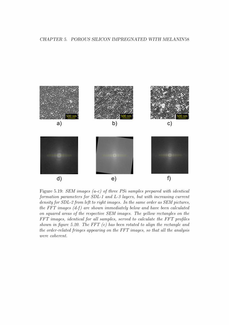
CHAPTER 5. POROUS SILICON IMPREGNATED WITH MELANIN58
500 nm 500 nm 500 nm
a) b)
d)
c)
e) f)
Figure 5.19: SEM images (a-c) of three PSi samples prepared with identicalformation parameters for SDL-1 and L-3 layers, but with increasing currentdensity for SDL-2 from left to right images. In the same order as SEM pictures,the FFT images (d-f) are shown immediately below and have been calculatedon squared areas of the respective SEM images. The yellow rectangles on theFFT images, identical for all samples, served to calculate the FFT profilesshown in figure 5.20. The FFT (e) has been rotated to align the rectangle andthe order-related fringes appearing on the FFT images, so that all the analysiswere coherent.
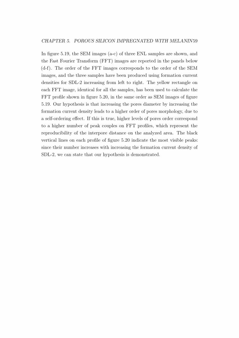
CHAPTER 5. POROUS SILICON IMPREGNATED WITH MELANIN59
In figure 5.19, the SEM images (a-c) of three ENL samples are shown, andthe Fast Fourier Transform (FFT) images are reported in the panels below(d-f). The order of the FFT images corresponds to the order of the SEMimages, and the three samples have been produced using formation currentdensities for SDL-2 increasing from left to right. The yellow rectangle oneach FFT image, identical for all the samples, has been used to calculate theFFT profile shown in figure 5.20, in the same order as SEM images of figure5.19. Our hypothesis is that increasing the pores diameter by increasing theformation current density leads to a higher order of pores morphology, due toa self-ordering effect. If this is true, higher levels of pores order correspondto a higher number of peak couples on FFT profiles, which represent thereproducibility of the interpore distance on the analyzed area. The blackvertical lines on each profile of figure 5.20 indicate the most visible peaks:since their number increases with increasing the formation current density ofSDL-2, we can state that our hypothesis is demonstrated.
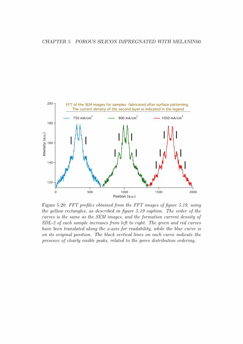
CHAPTER 5. POROUS SILICON IMPREGNATED WITH MELANIN60
200
180
160
140
120
Inte
nsity
(a.
u.)
2000150010005000Position (a.u.)
750 mA/cm2 900 mA/cm2
1050 mA/cm2
FFT of the SEM images for samples fabricated after surface patterning. The current density of the second layer is indicated in the legend
Figure 5.20: FFT profiles obtained from the FFT images of figure 5.19, usingthe yellow rectangles, as described in figure 5.19 caption. The order of thecurves is the same as the SEM images, and the formation current density ofSDL-2 of each sample increases from left to right. The green and red curveshave been translated along the x-axis for readability, while the blue curve ison its original position. The black vertical lines on each curve indicate thepresence of clearly visible peaks, related to the pores distribution ordering.

CHAPTER 5. POROUS SILICON IMPREGNATED WITH MELANIN61
5.3 Large-pores samples with eumelanin
The new porous matrices produced by using the ENL process described in5.2 have been used to be impregnated with melanin in order to investigatethe effect of the pores size on the polymer behvior. According to the hy-pothesis made at the end of section 5.1, the polymer inside the pores shouldbehave differently depending on pores dimension, and this could influence thetemporal stability of the samples in terms of photocurrent production. Thetechnical details of samples fabrication through ENL process are reported insection 4.1.1. The final step of samples fabrication has been a treatment witha diluted 0.1 M NaOH solution for 60 s in order to enlarge the pores diameterand reduce the surface asperities inside the pores: plane view SEM imagesreveal that there is an increase in the pores opening from about 34 nm to about60 nm while, from the cross-section analysis, a reduction of the dendriteslength is also visible after the NaOH treatment. The impregnation of thepores with the eumelanin solution has been done according to the proceduredescribed in 4.2.1, and the effect of three different monomer concentrationshas been investigated: 8mgml�1, 16mgml�1 and 24mgml�1. The lowerconcentration is the same that has been used in 5.1 for thin-pores samples,while the others have been chosen because the enlargement of the poresmay affect the solution mobility and a new optimization of the impregnationprocess could be necessary.
In figure 5.21 are shown the first results obtained with the new PSimatrix: white-light photocurrent has been measured for several days forthe ENL samples impregnated with three different DHI concentrations, andthey have been compared with the white-light photocurrent produced by anempty sample and with that of a 10 nm-diameter sample impregnated withan 8mgml�1 concentrated DHI solution. First of all, no significant differenceas a function of the DHI concentrations was noted, but an enhancementof the white-light photocurrent generation with respect to the empty andto the impregnated PSi with thinner pores is quite clear. Moreover, animprovement in the temporal stability of the samples is also evident, sincephotocurrent values after 10 days from the samples fabrication were more or

CHAPTER 5. POROUS SILICON IMPREGNATED WITH MELANIN62
Figure 5.21: Temporal evolution of white-light photocurrent of samples obtainedwith ENL procedure and impregnated using three different DHI concentrations:8mgml�1, 16mgml�1 and 24mgml�1. These curves are also compared withthe white light evolution of an empty PSi sample made with ENL procedure, andwith that of a standard PSi sample impregnated with an 8mgml�1 concentratedDHI solution.
less the same as the first day, differently from what happens in case of thinnerpores samples (section 5.1). After a slower decay with respect to the sampleswith thinner pores, still measurable photocurrent values were recorded after20 days, and they remain quite constant in the following weeks. Anothersignificant improvement compared to the past is the reproducibility of thephotocurrent intensity from sample to sample. As it is visible from figure 5.21,for large pores samples photocurrent values are independent of the detailsof the fabrication process and are very similar to one another, while for thinpores there were huge variations spanning over orders of magnitude (100 nAto 700 µA).
In figure 5.22 the spectral behaviour of the samples shown in figure 5.21 isreported, again measured for many days in order to observe the temporalevolution. The comparison with the spectral behaviour of an empty PSi

CHAPTER 5. POROUS SILICON IMPREGNATED WITH MELANIN63
Figure 5.22: Time evolution of the spectral behaviour of the samples im-pregnated with different DHI concentrations: 8mgml�1, 16mgml�1 and24mgml�1. The spectral behaviour of an empty PSi matrix is also shown forreference in bordeaux in each panel, and the green arrows roughly indicate theevolution of the photocurrent spectra with time.

CHAPTER 5. POROUS SILICON IMPREGNATED WITH MELANIN64
sample is reported in each panel. As it is visible from these graphs, anincrease of the eumelanin-induced spectral absorption is a common featurefor all the samples, due to the polymerization of DHI inside the pores. Theinteresting characteristic, that is common for all the samples and that was notvisible for samples with thinner pores, is that the effect of eumelanin seems toincrease over time, as the green arrow indicates; moreover, the photocurrentgeneration stops to decrease with time and tends to stabilize after about 20
days. In analogy to what happens to the absolute photocurrent, also thestabilization of the spectral response occurs after about 20 days, as evidencedin figure 5.21. This stabilization was not observed for samples with thinnerpores, so there is a clear dependence between sample characteristics andpores dimension. These results in terms of photocurrent stability demonstratethe accuracy of the hypothesis that we made thanks to the computationalstudy on polymer behaviour depending on pores dimension (section 5.1). Wecan eventually state that the introduction of larger pores does improve thestabilization of the hybrid junction, because the H2O2 produced during thepolymerization process diffuses slower toward the silicon walls with respectto thinner pores samples. This result is in agreement with other literatureworks that demonstrate the pore diameter dependence on the final propertiesof a porous device [145,146].
5.4 MACE nanostructured porous silicon with
eumelanin
One of the strategies for improving the efficiency of a photovoltaic device isthe optimization of light absorption. The addition of melanin itself is aimed atenhancing the photoconductivity of the final device: its absorption properties,in fact, allow to increase the absorption coefficient for thin layers and thisshould, in principle, permit to reduce the final thickness of the photovoltaicdevice. Moreover, part of the light that impinges on a photovoltaic deviceis reflected by the surface itself, so it cannot contribute to the productionof photovoltaic energy. Minimizing that loss, a larger part of the incident

CHAPTER 5. POROUS SILICON IMPREGNATED WITH MELANIN65
1 µm 1 µm
100 nm 100 nm
Figure 5.23: SEM images in cross-section and plane-view of samples obtainedby MACE using Pt (left-side) and Ag (right-side) metal nanoparticles.
photons can be used to produce electron-hole pairs, and then also the efficiencyof the device can be positively affected. Many research efforts are devotedto improve the anti-reflection properties of solar cells [147–152] and PSiitself has been studied also for that purpose [153–155]. Besides throughelectrochemical etching, PSi can be produced with an electroless techniquecalled metal-assisted chemical etching (MACE), as explained in section 2.1.2.
Thanks to the fact that the interface between porous and bulk silicon as-sumes a very typical pyramidal shape, the reflectivity of these samples isorders of magnitude lower than the one of standard PSi obtained with theelectrochemical etching. Combining together the antireflection propertiesof the MACE PSi samples with the absorption properties of eumelanin, itwould be possible, in principle, to optimize the photovoltaic properties of suchhybrid heterojunction and to produce thinner device. Present technology,in fact, is affected by the need of using thick layer of absorbing material tocompensate the problem of indirect bandgap of Si, that limits its photovoltaicefficiency. In this paragraph, a preliminary study on the realization of a hy-brid heterojunction made with MACE PSi filled with eumelanin is presented.This study has started in 2016 in collaboration with the group of S. Bastide

CHAPTER 5. POROUS SILICON IMPREGNATED WITH MELANIN66
Figure 5.24: Specular reflectivity of the different phases of the samples real-ization, both for Pt samples (left side) and Ag samples (right side).
of CNRS-ICMPE in Thiais (France) and has culminated with my stage inthose laboratories for four months in 2018; samples fabrication and theiranalysis with SEM has been done in France, while samples impregnation withmelanin and their optical analysis have been performed both in Thiais andin Cagliari. Two different metal nanoparticles have been used as catalyticagents for MACE: silver and platinum. In figure 5.23 SEM images of the twotypes of samples have been presented, both in-plane view and in cross-section:left-side images are of a sample prepared using Pt nanoparticles as metalcatalyst, while right-side images are of a sample prepared with Ag. Bothtypes of morphologies have been studied, since it was not possible to know inadvance which configuration would be better: Pt-samples have a flat uppersurface but the diffused porosity among the nanoparticles channels is verynarrow, so it could be a problem for the organic solution to penetrate; onthe other hand, Ag-samples have more diffused larger pores, but the uppersurface is very rough, and that could be a problem for the deposition of thegold contact on top.
All the samples have been impregnated according to the procedure describedin 4.2.1 and have been analyzed with a UV-Vis-NIR spectrophotometer tomonitor all the phases of the sample preparation: after the sample realization,after the impregnation with the monomer solution, after the polymerizationprocess and after the deposition of the gold surface contact (figure 5.24). As

CHAPTER 5. POROUS SILICON IMPREGNATED WITH MELANIN67
visible from these graphs, the polymerization process (dark brown curves)can have either the effect of decreasing (left case) or increasing (right case)the samples reflectivity with respect to the reflectivity of the sample freshlyimpregnated with the monomer solution (light brown curves). The decreasingof the reflectivity, reported in case of impregnated samples obtained withPt nanoparticles, is an expected behaviour when an absorbing materiallike eumelanin is inserted in the PSi matrix. On the contrary, a possibleexplanation of the behaviour reported for the Ag samples could be related tothe morphological aspect of the samples surface, that are more rough withrespect to the surfaces of the previous samples. In this case, the flatteningof the surface due to the deposition of the eumelanin solution could be theexplanation of the increase of the sample reflectivity. The decrease of thesample roughness could be more relevant than the insertion of an absorbingmaterial on the final optical properties. To verify the impregnation of thePSi matrix with the organic solution, the samples have been analyzed bySEM-EDS. The atomic percentage of carbon with respect to silicon has beenmeasured at the top and at the bottom of the porous layer for both thematrices. The results are reported in table 5.4 and they show a typicalgradient from the top to the bottom in the pores impregnation.SEM-EDSanalysis showed good results that confirm the impregnation of the poreswith melanin; however, it has not been possible to characterize the samplesfrom the photocurrent point of view. In fact, even if a weak photocurrentresponse was visible for some of the samples, their values were too low andtoo noisy to be measurable and analyzed. One of the problems to be solvedthat prevents photocurrent measurements is the surface roughness, especiallyfor samples made with Ag nanoparticles. This issue limited the possibility todeposit a thin and homogenous metallic layer as a top contact to collect theseparated charges at the interface of the junction. With such a roughness,the percolation threshold to have a uniform gold contact on the top surfaceby sputtering is reached for a longer deposition time with respect to a flatsurface.
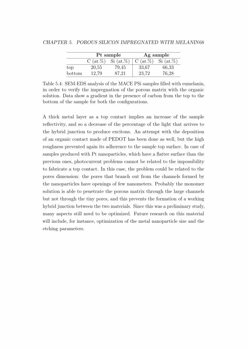
CHAPTER 5. POROUS SILICON IMPREGNATED WITH MELANIN68
Pt sample Ag sample
C (at.%) Si (at.%) C (at.%) Si (at.%)top 20,55 79,45 33,67 66,33bottom 12,79 87,21 23,72 76,28
Table 5.4: SEM-EDS analysis of the MACE PSi samples filled with eumelanin,in order to verify the impregnation of the porous matrix with the organicsolution. Data show a gradient in the presence of carbon from the top to thebottom of the sample for both the configurations.
A thick metal layer as a top contact implies an increase of the samplereflectivity, and so a decrease of the percentage of the light that arrives tothe hybrid junction to produce excitons. An attempt with the depositionof an organic contact made of PEDOT has been done as well, but the highroughness prevented again its adherence to the sample top surface. In case ofsamples produced with Pt nanoparticles, which have a flatter surface than theprevious ones, photocurrent problems cannot be related to the impossibilityto fabricate a top contact. In this case, the problem could be related to thepores dimension: the pores that branch out from the channels formed bythe nanoparticles have openings of few nanometers. Probably the monomersolution is able to penetrate the porous matrix through the large channelsbut not through the tiny pores, and this prevents the formation of a workinghybrid junction between the two materials. Since this was a preliminary study,many aspects still need to be optimized. Future research on this materialwill include, for instance, optimization of the metal nanoparticle size and theetching parameters.
Chapter 6
Porous silicon impregnated with
erbium
In this chapter, the results obtained on the study of PSi samples impregnatedwith erbium are presented. In particular, section 6.1 reports a little back-ground on the previous studies on Er-doped PSi samples, where the limit inPL emission due to erbium clustering is highlighted. In section 6.2, instead,an alternative idea to overcome the erbium clustering issue and to enhancethe Er-related PL emission is presented through a multidisciplinary studythat involves electrochemical, morphological and optical techniques.
6.1 A little background on Er-doped PSi: pho-
toluminescence intensity issue
PL production from pure silicon devices is prevented by the fact that siliconhas an indirect bandgap; radiative recombination between an electron-holepair in this type of semiconductor, in fact, can occur only in case of absorptionor emission of a phonon. To overcome this limitation, hybrid silicon-baseddevices have been proposed [156], but they are generally quite complex andexpensive solutions. Another possibility could be to exploit the PL emissionof PSi, discovered at the beginning of the 1990s, probably due to quantumconfinement effect on its crystalline structure [157, 158], or the doping of
69

CHAPTER 6. POROUS SILICON IMPREGNATED WITH ERBIUM 70
PSi itself with rare earths. In fact, it has been demonstrated that rare-earth doped PSi structures can emit light at � = 1.5 µm [159–165], thatfalls in the transparent transmission wavelengths window of silica opticalfibers [166]. The origin of the erbium PL comes from electron intra-4ftransitions of the incomplete shell; this transition switches from forbiddento partially allowed when the ion Er3+ passes from the free ion state tobeing hosted in a non-centrosymmetric site [167–169]. Many efforts havebeen done in rare-earth doping of silicon structures [170, 171], includingalso the co-doping with erbium and ytterbium [172,173], but unfortunatelynot enough high yield PL has been obtained so far [82, 174]. It has beendemonstrated that erbium clustering plays a major role in preventing theproduction of efficient Er-doped luminescent devices. The alternative pathsthat have been followed by researchers to overcome this limit were eitherthe use of erbium-doped Silicon Rich Oxide (SRO) structures [175–181] orthe lowering the erbium doping levels [82]. Several works have been madeon the study of the electrochemical doping of PSi samples [30, 83–86] inorder to understand the origin of the low PL intensity. In particular, inreference [85] it has been reported that the evolution of the applied voltage ofthe electrochemical doping shows different shapes depending on the currentintensity used to perform the process. More precisely, for low currents a singletransient is evident, and the voltage absolute value monotonically increases asthe process goes on; for higher currents, instead, a double transient appearsin the voltage evolution, meaning that two different Er deposition processesare involved. The study of the initial phases of the electrochemical dopingby means of GEIS (Galvanostatic Electrochemical Impedance Spectroscopy)permitted to propose a possible interpretation of this behaviour. Actually,two processes are induced by the applied electric field during Er deposition:one is the migration of the Er3+ ions present in the electrochemical solutiontowards the inner pores surface, the other is the transfer of the charge fromthe ions to the solid structure. When using high electric fields, which meanshigh current values, the flux of the Er3+ ions is more intense and leads to aconsistent ions accumulation near the PSi top surface up to the formationof a jelly-like layer. This does not happen in case of low doping current and

CHAPTER 6. POROUS SILICON IMPREGNATED WITH ERBIUM 71
this difference can explain the different behaviours of the voltage evolutionin the two regimes. Moreover, the applied current intensity also influencesthe final erbium content deposited on identical PSi samples, keeping constantthe transferred charge. In fact, structural characterization of the sampleswith SEM-EDS microscopy permitted to measure the Er percentage, atvarious depths, in nominally identical samples doped with high (0.5mA) andlow (0.05mA) current intensities. The measurements showed that the Erpercentage in the first case (high current intensity) is higher with respect towhat has been measured in the second case (low current intensity). Giventhe higher efficiency of the process in high current regime, this condition hasbeen used to perform the study reported in this dissertation.Starting from these discoveries, a more detailed study on the electrochemicaldoping process of PSi samples has been carried out and presented here. Thefirst step of the study was the electrochemical impregnation of a PSi samplewith an erbium quantity of around 1%. The sample has been fabricatedaccording to the procedures reported in 4.1.1, while the impregnation ofthe pores with erbium has been done through the electrochemical processdescribed in 4.2.2. The 1% doping level corresponds to the amount of erbiumthat is typically inserted in erbium-doped light-emitting PSi samples andfor which erbium clustering appears. On such a sample, ET analysis hasbeen carried out in Grenoble following the procedures described in 4.3.2. Theresults are shown in figure 6.1. Both in sagittal and in axial slices the erbiumclusters are visible as white spots randomly spread on the walls of the pores.In fact, since ET is very sensitive to the atomic number Z, erbium appearsmuch brighter than silicon because its Z is much higher than that of Si.

CHAPTER 6. POROUS SILICON IMPREGNATED WITH ERBIUM 72
(A)
(C) (F)
(B) (E)
(D)
(B)
100 nm
Figure 6.1: ET images, both in sagittal slices and in axial slices, of an Er-doped PSi sample with an erbium percentage of 1%, calculated by SEM-EDSmapping. Axial sections are extracted in correspondence of the white linesreported in panels (A), (B) and (C); at the same way, sagittal images aretaken in correspondence of the white lines of panels (D), (E) and (F).
6.2 A new approach: pores filling for photolu-
minescence improvement
The scope of the work proposed here is to have a deeper understanding of theelectrochemical doping process; in fact, the optimization of this crucial phaseof samples preparation would permit to better understand the PL origin andto enhance the final properties of this composite material. The strategy thathas been adopted here to overcome the erbium clusters issue goes in theopposite direction with respect to the idea proposed by Prtljaga et al. inreference [82]: instead of reducing the erbium amount to prevent the clustersformation, the strategy to greatly increase the doping quantity inside thepores has been explored. Several PSi samples have been prepared, followingthe electrochemical procedure described in 4.1.1, and then electrochemicallyfilled with erbium in galvanostatic regime, as explained in 4.2.2, with dopinglevels of 1.2, 4.0, 6.0, 8.0, 10.0, 12.0% (table 6.1).

CHAPTER 6. POROUS SILICON IMPREGNATED WITH ERBIUM 73
Er doping time (s) Er concentration (%)
25 130 1.2100 4150 6200 8250 10300 12
Table 6.1: Equivalence between duration of the Er doping and the Er concen-tration, measured through SEM-EDS for 1.3 µm thick samples doped using aconstant doping current of 1mA.
In figure 6.2, the voltage evolution for a 12% electrochemical doping processis presented. Three different transients in the voltage evolution are visibleand indicated with green references in the graph: as already mentionedin reference [85], to each transient corresponds a different phase in poresdoping process. To activate the Er-luminescence, in both crystalline [182,183]and PSi layers [184, 185], a thermal treatment must be mandatory; in thiscase, samples have been subjected to an annealing process at 700 �C in N2
inert atmosphere, with the scope to have an efficient Er activation withoutsignificantly changing the pores structure. In fact, if 700 �C is relatively lowcompared with the optimal temperature for PL performance of Er silicate andEr oxide [186,187], it is also good for preservation of the PSi matrix [188] andto avoid the induction of structures that would be similar to silicon-rich-oxide.Both structural and optical characterizations have been performed on thesamples as a function of the erbium doping level, from 1.2%, that is thestandard doping level also mentioned in the previous paragraph, up to 12%,that corresponds to a surface accumulation of Er ethanolate gel visible bynaked eye.
Er-doped PSi samples have been characterized from the structural point ofview in Grenoble by ET. In figure 6.3, ET images of two Er-doped PSi samplesare presented: panels (A) to (F) refer to a as-prepared 1.2% doped sample,while panels (G) to (L) refer to an annealed 8% doped sample. In these
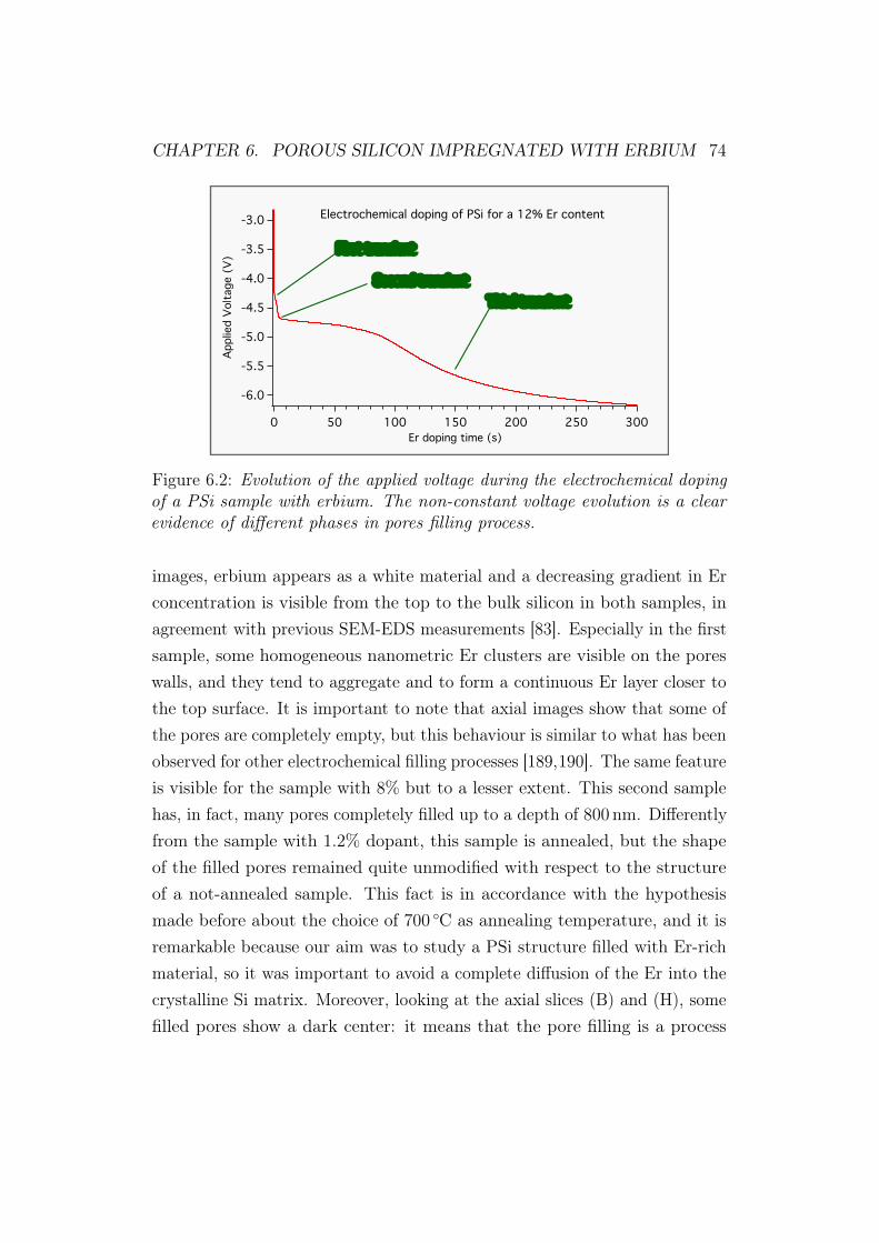
CHAPTER 6. POROUS SILICON IMPREGNATED WITH ERBIUM 74
-6.0
-5.5
-5.0
-4.5
-4.0
-3.5
-3.0Ap
plie
d Vo
ltage
(V)
300250200150100500Er doping time (s)
First transient
Second transientThird transient
Electrochemical doping of PSi for a 12% Er content
Figure 6.2: Evolution of the applied voltage during the electrochemical dopingof a PSi sample with erbium. The non-constant voltage evolution is a clearevidence of different phases in pores filling process.
images, erbium appears as a white material and a decreasing gradient in Erconcentration is visible from the top to the bulk silicon in both samples, inagreement with previous SEM-EDS measurements [83]. Especially in the firstsample, some homogeneous nanometric Er clusters are visible on the poreswalls, and they tend to aggregate and to form a continuous Er layer closer tothe top surface. It is important to note that axial images show that some ofthe pores are completely empty, but this behaviour is similar to what has beenobserved for other electrochemical filling processes [189,190]. The same featureis visible for the sample with 8% but to a lesser extent. This second samplehas, in fact, many pores completely filled up to a depth of 800 nm. Differentlyfrom the sample with 1.2% dopant, this sample is annealed, but the shapeof the filled pores remained quite unmodified with respect to the structureof a not-annealed sample. This fact is in accordance with the hypothesismade before about the choice of 700 �C as annealing temperature, and it isremarkable because our aim was to study a PSi structure filled with Er-richmaterial, so it was important to avoid a complete diffusion of the Er into thecrystalline Si matrix. Moreover, looking at the axial slices (B) and (H), somefilled pores show a dark center: it means that the pore filling is a process

CHAPTER 6. POROUS SILICON IMPREGNATED WITH ERBIUM 75
(A)
(C)
(E)(G)
(I)
(K)
(B)
(D)
(F)
(H)
(J)
(L)
Needle‑ET for a PSi_1.2%
sample
Needle‑ET for a PSi_8%
_A sample
Figure 6.3: ET of Er-doped PSi samples: panels (A) to (F) refer to a not-annealed 1.2% doped sample, while panels (G) to (L) refer to an annealed 8%doped sample. Panels on the left are different sagittal slices, while panels onthe right are different axial slices in the 3D reconstructed volume. Localizationof the sagittal slices is represented by a white line on the corresponding axialslices and vice versa. The top surfaces of PSi samples are on the left-handside of the figure. The filling of the pores by the Er deposition is evidenced bythe white signal from the PSi pores.

CHAPTER 6. POROUS SILICON IMPREGNATED WITH ERBIUM 76
Figure 6.4: SEM-BSE image of an annealed PSi sample with 8% Er.
that starts from the pores surface and proceeds towards the center. This isan important information that permits to understand how the impregnationworks and to give a better interpretation of the voltage evolution duringthe electrochemical doping. Another morphological characterization of thesesamples has been done by the group of A. Falqui at KAUST (Saudi Arabia)using SEM-BSE technique. In figure 6.4, a top view SEM-BSE image of anannealed PSi sample with 8% Er is reported and several things can be noted.Given the high sensitivity of SEM-BSE to the elements atomic number, theEr-filled pores appear like white spots, while dark spots are empty pores, inanalogy with ET observations. Moreover, some areas with diffused brightnesscan be noticed, and these indicate a surface coverage that appears when mostof the pores are completely filled.
The samples have also been analyzed in collaboration with the group of M.Saba of the University of Cagliari to explore their PL properties. In figure 6.5are shown the PL intensity results for samples with different doping levelsafter the annealing treatment. Each spectrum is normalized with respectto the maximum intensity of the silicon emission (� < 1200 nm) for easier

CHAPTER 6. POROUS SILICON IMPREGNATED WITH ERBIUM 77
(d)(c)
(b)(a)
Figure 6.5: Normalized PL results from annealed PSi samples with differentEr content.
comparison. Looking at the peak at � = 1540 nm, it seems that the higheris the Er content, the higher is the PL intensity. A maximum is reachedfor doping level of 8%, and then a slight reduction and saturation of themaximum PL value is observed for higher doping levels.
On the samples that showed a significant PL emission, time-resolved PLmeasurements have been also performed, again in collaboration with thegroup of M. Saba. These measurements have been performed on 6, 8, 10 and12% after the annealing treatment and were intended to reveal any differentoptical properties of the composite material. The results are presented infigure 6.6: the red curve, that is referred to the sample with 6% Er, ischaracterized by two decay times: a faster one (⌧1 = 3.6 µs) and a slowerone (⌧2 = 20 µs), and they have been obtained by fitting the experimentaldata with a biexponential curve. All the other samples have a single fastdecay time quite similar to ⌧1 and they are all characterized by an Er-richfilm on the top surface, as demonstrated in [83]. The magenta curve, instead,

CHAPTER 6. POROUS SILICON IMPREGNATED WITH ERBIUM 78
(d)(c)
(b)(a)
Figure 6.6: Time-resolved PL results from annealed samples with differentEr content and the relative decay times obtained by fitting the curves withexponential functions. The purple line with the shorter decay time is referredto a bulk Si wafer with a thick Er-rich layer deposited on top using the samesolution and doping current used for the doping of the porous samples.
represents the behaviour of a relatively thick Er layer deposited on a bulkSi sample using the same electrochemical deposition process but for a longerduration (2000 s). This different sample has a faster decay time of ⌧ = 2.5 µs,while the time resolution of the set-up, measured as the apparent duration ofa sub-picosecond laser pulse, was around 1 ns.
In order to understand if the emitted light came predominantly from fewhotspots or homogeneously from all the sample surface, micro-PL measure-ments have been evaluated. In figure 6.7 (a) micro-PL measurements of anannealed PSi sample with 8% Er is shown, while in (b) is reported the corre-sponding bidimensional mapping: the intensity of each point on the map hasbeen taken as the integrated intensity over the red area in the correspondingspectrum. Looking at the results, PL emission is quite homogenous in all the

CHAPTER 6. POROUS SILICON IMPREGNATED WITH ERBIUM 79
Figure 6.7: (a) Micro-PL measurements of an annealed PSi sample with8% Er; (b): bidimensional mapping of micro-PL results shown in (a): theintensity of each point on the map has been taken as the integrated intensityover the red area in the corresponding spectrum.
map, with small intensity fluctuations compatible with small local Er contentdifferences and little local surface asperities.
All the results of this work can be summarized in figure 6.8: the evolutionof the electrochemical doping process is represented with the red curve, thatis the voltage as a function of the Er content (using table 6.1 to convertdoping time in erbium percentage); PL data are taken from figure 6.5 andare indicated as coloured rectangular bars, one for each analyzed dopinglevel (vertical black lines). As already mentioned, the applied voltage is notconstant during the Er doping, and the various transients are an indicationof different doping regimes. The first double transient had been alreadystudied [30,83–85] and has been attributed to the formation of a surface layerof Er ethanolate gel, whose higher density facilitates the ions permanenceinside the pores.
After the first double transient, the voltage remains approximately constant:the ET result on the 1.2% doped sample suggests that this is the phase whereEr accumulates in the pores walls in form of small nanoclusters or thin filmnear the top surface. As the electrochemical doping process goes on, the Erfilling starts from the pores walls and continues to their center. This was

CHAPTER 6. POROUS SILICON IMPREGNATED WITH ERBIUM 80
PL in
tens
ity (a
.u.)
%121086420
Er amount
Figure 6.8: Synoptic representation of the results about the Si pores filling withEr. The red curve represents the evolution of the applied voltage during theelectrochemical doping in galvanostatic regime; the black lines across the curveindicate the Er doping levels that have been presented in the text. Immediatelyabove them, the colored rectangles represent the PL intensity corresponding tothe various doping levels. Finally, thanks to morphological characterization, ithas been possible di identify the different phases of the doping process, whoselabels are reported under the PL results.

CHAPTER 6. POROUS SILICON IMPREGNATED WITH ERBIUM 81
evident from ET (figure 6.3, panels (G) to (L)) of the 8% doped-sample,where the dark core of the filled pores was visible. In this phase, the increaseof the voltage absolute value is due to the reduction of the pores effectivediameter that progressively increases the voltage needed to move the Er ionsinside them. From SEM-BSE analysis (figure 6.4) of the same sample, instead,the Er surface accumulation emerged, coherently with the results reportedin reference [83], and it progressively continues as the doping level increases.Then, thee different regimes in the doping process can be identified: (A) Ergel formation, (B) pore filling and (C) a contemporaneous pore filling andsuperficial film accumulation. It is interesting to compare the three regimeswith the corresponding PL results: when the amount of erbium is very low(1.2%) a weak PL emission is measured; when the Er content increases, sohappens to PL emission. The maximum intensity is measured for the samplewith 8% Er-level, which corresponds to the beginning of the superficial filmdeposition. This could be explained by the fact that the Er-rich materialinside the pores is more efficient than the surface coverage in PL emission,which tends to decrease when the surface accumulation covers the entiresample. Another important information on these types of samples can beobtained by the measurements of the decay times of the PL emission (figure6.6). The sample with 6% Er-doping showed two different decay times, onefaster and one slower, and it had no surface Er layer since it is below thesurface accumulation threshold. All the samples with a higher Er level, whichalso have a surface accumulation on top, exhibited one only short decay time.These observations can help to attribute a double origin to the PL emission:the thermal annealing produces an erbium silicate inside the pores near thewalls, while erbium oxide is produced elsewhere. The first one is characterizedby a slower decay time, while the second exhibits a faster emission and thishypothesis is supported by the two literature works [186, 187]. From thisanalysis, it is possible to hypothesize that the light emission from sampleswith Er-rich film coverage is mainly due to Er oxide, while the emissionwithout the superficial layer mainly comes from Er silicate that is inside thePSi matrix.

CHAPTER 6. POROUS SILICON IMPREGNATED WITH ERBIUM 82
6.3 Er-doping of large-pores samples
Since a more regular structure and a larger diameter have a great influencein solution mobility inside the pores, the modification of the porous matrixcan bring a further improvement in the electrochemical impregnation witherbium. For this reason, we used the ENL protocol to fabricate PSi sampleswith larger pores, and we made some preliminary studies on the effect of thenew porous matrix on the impregnation process with the erbium solution.
The technical parameters for PSi samples preparation using the ENL protocolare reported in section 4.1.1, while the electrochemical doping with Er hasbeen performed in the same way as standard samples, according to theprocedure explained in 4.2.2. Figure 6.9 shows the comparison between theapplied voltage evolution measured during the electrochemical doping withEr of a PSi sample fabricated using ENL (a) with the analogous evolutionobtained in case of a standard PSi doping (b). The two graphs refer to thesame doping time, that is 300 s, and the evolution of the applied voltage issimilar in both cases. In particular, the transients that indicate the variousphases of the electrochemical doping are visible also for ENL samples. SEMcharacterizations using backscattered electrons (SEM-BSE) show that the Erpenetration within the pores is significantly improved in case of ENL samples,since the images show a full filling in the whole pores length. Since the newpores are larger and less dendritic as compared with standard samples, thisresult can be explained with the improved mobility of the solution withinthe larger pores. Of course, this difference also reflects onto the specifictransient shape. If, on one side, the presence of the different transient inboth thin- and large-pore samples demonstrates that the process is the samein both cases, on the other side the details of the transients depend on thespecific pores characteristics. For instance, larger pores do not imply higherporosity, that is larger volumes within the pores, but a better penetrationof the pores may compensate a lower porosity: the position of the thirdtransient, the one related to the pores filling process, will depend from thedetails of the fabricated pores. All these aspects require a detailed study
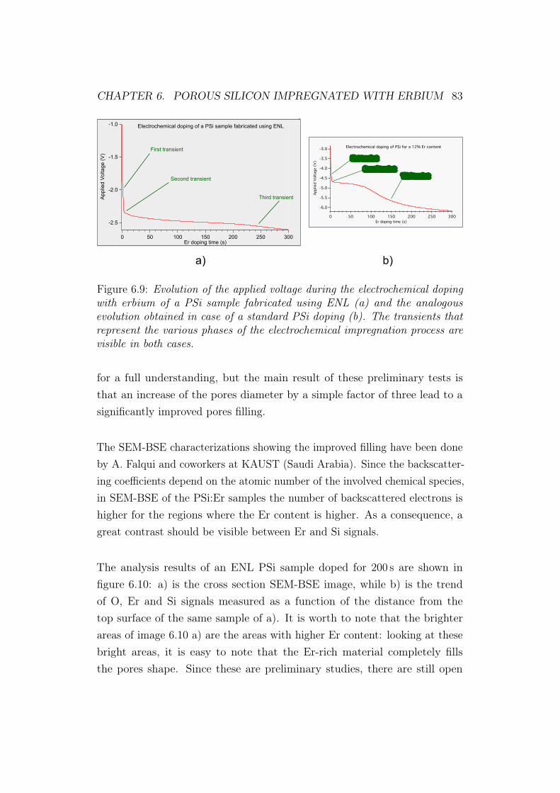
CHAPTER 6. POROUS SILICON IMPREGNATED WITH ERBIUM 83
-2.5
-2.0
-1.5
-1.0
App
lied
Volta
ge (V
)
300250200150100500Er doping time (s)
Electrochemical doping of a PSi sample fabricated using ENL
First transient
Second transient
Third transient
-6.0
-5.5
-5.0
-4.5
-4.0
-3.5
-3.0
Appl
ied
Volta
ge (
V)
300250200150100500Er doping time (s)
First transient
Second transientThird transient
Electrochemical doping of PSi for a 12% Er content
a) b)
Figure 6.9: Evolution of the applied voltage during the electrochemical dopingwith erbium of a PSi sample fabricated using ENL (a) and the analogousevolution obtained in case of a standard PSi doping (b). The transients thatrepresent the various phases of the electrochemical impregnation process arevisible in both cases.
for a full understanding, but the main result of these preliminary tests isthat an increase of the pores diameter by a simple factor of three lead to asignificantly improved pores filling.
The SEM-BSE characterizations showing the improved filling have been doneby A. Falqui and coworkers at KAUST (Saudi Arabia). Since the backscatter-ing coefficients depend on the atomic number of the involved chemical species,in SEM-BSE of the PSi:Er samples the number of backscattered electrons ishigher for the regions where the Er content is higher. As a consequence, agreat contrast should be visible between Er and Si signals.
The analysis results of an ENL PSi sample doped for 200 s are shown infigure 6.10: a) is the cross section SEM-BSE image, while b) is the trendof O, Er and Si signals measured as a function of the distance from thetop surface of the same sample of a). It is worth to note that the brighterareas of image 6.10 a) are the areas with higher Er content: looking at thesebright areas, it is easy to note that the Er-rich material completely fillsthe pores shape. Since these are preliminary studies, there are still open

CHAPTER 6. POROUS SILICON IMPREGNATED WITH ERBIUM 84
a) b)
Figure 6.10: a) SEM-BSE image of an Er-doped PSi sample. b) behaviour ofO, Er and Si signals as a function of the distance from the top surface of thesample.
questions on the apparent inhomogeneity of the filling that will require furtherinvestigations. These results indicate that filling of larger pores is, as expected,more effective for the homogeneous filling in the whole pore length, that is1.7 nm in this case. If we compare these results with ET images of Er-dopedstandard PSi samples reported in section 6.2, we notice that the thin poreswere filled up to a length of 800 nm, even if the thickness of the porous layerwas about 1.3 µm. For standard samples, therefore, the highly dendriticstructure and the small openings do not permit the solution to efficientlymove within the pores and therefore to have a sufficient exchange with theexternal solution to keep the Er concentration constant in the whole poreslength. Moreover, small Er accumulation within the thin pores will lead tosignificant reduction of the available pores diameter even with small deposits.Since the solution mobility depends on the square of the pores radius, theconsequence is that the filling of the pores can be significantly improvedby small increase in their diameter. In summary, the possibility to fill thepores depends strongly on the pore diameter and it appears that significantimprovements in the pores filling can be achieved even with relatively smallincreases in the pore diameter. Although this strategy still needs further

CHAPTER 6. POROUS SILICON IMPREGNATED WITH ERBIUM 85
studies, the full pores filling shown by the SEM-BSE images demonstratethat this approach is a very promising route towards high pores filling andtherefore highly photoluminescent materials.

Chapter 7
Porous silicon impregnated with
nickel
This last chapter is intended to present another application of the impregnationof PSi with a metallic material. This study has been possible thanks tothe competencies that we acquired on PSi impregnation, in this case withelectrochemical methods. In section 7.1, in fact, the results obtained onPSi samples electrochemically filled with nickel are proposed with the aimof obtaining a new protocol for analysis and accurate reconstruction ofnanoporous materials by APT.
7.1 Nickel in porous silicon for a better atom
probe tomography reconstruction
The aim of the work presented in reference [101] was to propose a new protocolfor analysis and accurate reconstruction of nanoporous materials by APT.A study on this topic was then possible thanks to the collaboration with I.Mouton and coworkers from CEA-LETI and Université Grenoble Alpes; infact, our expertise in pores filling, especially through electrochemical processes,has been put together with their expertise in reconstruction techniques tofind a way to perform reliable APT reconstruction on porous materials.APT is a material analysis technique that allows the 3D reconstruction of a
86

CHAPTER 7. POROUS SILICON IMPREGNATED WITH NICKEL 87
specimen at the atomic scale, with around 0.1-0.3 nm in depth and 0.3-0.5nm lateral resolutions. It is based on the field evaporation of atoms from thetip of a needle-shaped portion of a sample, and the current reconstructionalgorithm is based on a geometric model that works as a point projectionof ion position on a hemispherical surface [191]. What is critical in thisprocess is the accurate evaluation of the reconstruction parameters, in orderto obtain a reliable spatial reconstruction of the real specimen. This processis quite easy in case of metallic materials, since the calibration is basedon lattice planes or desorption patterns [192], while it is complicated forsemiconductors and multiphase materials, where the projection laws affectthe reconstruction parameters, and the evaporation fields could be differentfrom one phase to another [193,194]. As a matter of fact, APT analysis andreconstruction with porous materials is quite a challenge: until now, the onlyway to make APT analysis possible is the filling of pores with 50 nm diameterwith electron beam induced deposition [195, 196]. To solve these problems,several research groups have proposed to improve algorithm [197] or constrainreconstruction [198–200] using other characterization techniques to integratecomplementary information. The most used technique is ET [201–203] becauseit allows discerning 3D nanoscale structure from a series of 2D projectionimages acquired at different tilt angles with a transmission electron microscope(TEM) [204].In this study, ET has been used together with APT on the same needle,taken from a nickel-impregnated PSi sample, in order to implement a newmodel for APT reconstruction. The reason why the two analysis techniqueshave been used together is that they allow a direct comparison between thereconstructed volume of the same sample, so that one can immediately knowhow good the reconstruction is by checking the correspondence of the tworesults. The analysis criterion is based on the proportion of well-positionedatoms for one APT reconstruction when compared to the ET reference volume.This correlation algorithm has been applied to mesoporous Si samples fortheir singular form of dendritic pores.
The samples were 1 µm thick with pores of 10 nm diameter, and they have

CHAPTER 7. POROUS SILICON IMPREGNATED WITH NICKEL 88
Figure 7.1: (a) HAADF STEM image of the whole tip with corresponding ETand APT analyzed volume respectively in red and blue. Slices in XZ and XYdirection from (b) the ET reconstruction with segmented volume for (c) nickeland (d) silicon element.

CHAPTER 7. POROUS SILICON IMPREGNATED WITH NICKEL 89
been electrochemically filled with nickel since it has a similar evaporationfield than silicon. The fabrication and impregnation of the samples havebeen performed at PoroSiLab in Cagliari (the details are reported in 4.1.1and ??, respectively), while all the analysis and their interpretation havebeen carried out by our collaborators in Grenoble. First of all, a check ofthe electrochemical filling and an observation of the microstructural features(pores size, morphology) has been done by using a FIB/SEM [205]. Then, toreduce electron beam damage and to have a large field of view, the analysishas been done on a needle of 200 nm diameter extracted from the poroussample. ET has been carried out on a FEI Titan Themis at 200 kV in HighAnnular Dark Field (HAADF) scanning electron transmission microscopy(STEM) using a 2050 Fishione holder with a tilt acquisition from �90° to 90°with steps of 1°. All the images have been denoised, aligned and reconstructedaccording to the procedures described by Printemps et al. in [104]. In figure7.1 (a) a HAADF STEM image of the needle extracted from the sample isshown. Different layers are visible starting from the top: a platinum cappingdeposited for sample preparation, a nickel layer, nickel-filled silicon pores andempty silicon pores. Figure 7.1 (b), instead, shows a yz-slice and an xy-sliceof the ET reconstruction, and the reconstructed volume is then segmentedusing global thresholding of the whole volume: in (c) nickel is evidenced ingreen, while silicon (d) in evidence in yellow. From ET reconstruction itis clear that pores are not damaged and are completely filled on 80 to 230nm from the top surface, and this makes possible APT experiments. To dothe APT analysis, the same needle has been afterwards reduced to achieve asharp curvature (around 50 nm), using a Cameca-Flextap in UV-laser pulsingmode (� = 343 nm). During the sample evaporation for reducing the needledimensions it has emerged the good adhesion and quality of the pores fillingwith nickel, since no irregular variation of the detection flux (or appliedvoltage) has been observed. For APT data reconstruction, a cone anglereconstruction algorithm [206] has been used, while 3D visualization is carriedout with Avizo software.In figure 7.2 the APT reconstruction has been shown: the top nickel layer isrepresented in green and the filled silicon porous layer is represented both in

CHAPTER 7. POROUS SILICON IMPREGNATED WITH NICKEL 90
Figure 7.2: APT reconstruction (e) of the nickel-filled porous sample withdensity map (in number of atoms) for (f) nickel and (g) silicon.
orange (the Si part) and green (the Ni part). Since the sample broke, only a50 nm thick portion of the nickel-filled porous layer has been observed withAPT. In ET reconstruction, images were composed of intensity voxels, while3D scatter plot has been collected for APT reconstruction, where each dotrepresents one reconstructed atom with a coordinates triad (x, y, z) and adifferent colour that means a different chemical nature. In order to makepossible the comparison of the two datasets, APT reconstruction is convertedinto a density map for each element, using the same voxel size as the ETreconstruction.
The number of atoms of the different elements is counted in all voxels allowingto generate a 3D density map (in number of atoms per voxel) for each element:figure 7.2 (f) and (g) are the 3D maps for nickel and silicon, respectively.

CHAPTER 7. POROUS SILICON IMPREGNATED WITH NICKEL 91
Figure 7.3: Correlation procedure between ET and APT.
This work aimed to find the best APT reconstruction parameters to fit theET 3D information (interface position, object size and morphology), and ascheme of the correlation procedure between ET and APT is shown in figure7.3. ET has been used to obtain a reference volume to force APT reconstruc-tion parameters, indicated with R0,↵. For each reconstruction parameter, ageometric transformation (rigid-body translations and/or rotations) must beapplied to APT reconstruction in order to maximise the matching betweenAPT and ET reconstructions. The optimization of the geometric transforma-tion requires also a matching quantification between ET and APT volumes;for this reason, the criterion of the proportion of well positioned atoms inAPT reconstruction as compared to the ET segmented volume has beenadopted. If an atom is consistent with the corresponding segmented voxelof ET, then a reconstructed atom is considered well positioned. Extendingthis argumentation for each atom, it is possible to determine a fraction ofwell-positioned atoms for a set of reconstruction parameters R0,↵. All thedetails about the optimization of the reconstruction algorithm can be found

CHAPTER 7. POROUS SILICON IMPREGNATED WITH NICKEL 92
Figure 7.4: Dependence of the APT reconstruction parameters R0,↵ on thefraction of well positioned atoms.
in reference [101], but it is worthy to underline is that the use of a well-filledPSi sample with mesopores of around 10 nm turned out to be successful forthe aim of the research. In fact, the fraction of well positioned atoms hasbeen calculated for a range of APT reconstruction parameters (cone anglealgorithm); in figure 7.4 the results on fraction of well positioned atoms as afunction of initial radius (R0 from 100Å to 600Å) and cone angle (↵ from 1°to 20°) are presented.
To conclude, this correlation methods turned out to work well with porousand nanostructured materials because the 3D features of the sample have welldistinctive shapes and the two elements Si and Ni have a quite different atomicnumber so that they can be clearly observed with the electron microscopesthanks to their chemical contrast.
Conclusion
The aim of this thesis was to study the impregnation of PSi matrices withdifferent materials and different techniques so that a better understanding ofthe process could optimize the final properties of the composite systems.The first part of the work was devoted to the study of PSi samples chemicallyfilled with melanin. The interest on this junction was born for its photovoltaicproperties, but the complexity of the materials involved required a moreaccurate comprehension of the two building materials themselves. In thissense, the photocurrent produced by the samples has been used in this disser-tation more as a mean to investigate materials and junction’s properties andstability. In chapter 5 the optimization of the samples impregnation in orderto improve the organic-inorganic junction stability has been presented. Thefirst parameters that have been investigated were expected to favour strongerchemical bonds between eumelanin and silicon. They were the modificationof the composition of the monomer solution and the functionalization of theinner surface of the pores through a light electrochemical oxidation, but theresults reported in section 5.1 showed that these had not a key role in theoptimization of the samples properties. Enlarging the pores diameter of oursamples of more than 50% (from 10-15 nm to 50-60 nm), it led to an increaseof the junction lifetime from one to several weeks. To fabricate samples with40-60 nm diameter pores that were also homogeneous in the size distributionand pores repartition, we developed a new electrochemical method for thelithography of the Si surface. The introduction of the ENL as a novel methodto produce PSi matrices allowed us to understand that pores dimension turnedout to be a fundamental parameter that highly affects the impregnation of aporous matrix.
93

CHAPTER 7. POROUS SILICON IMPREGNATED WITH NICKEL 94
In parallel with the chemical impregnation of PSi with melanin, we studiedthe electrochemical impregnation of PSi with metals. In chapter 6, the objectof the study was the impregnation of PSi samples with erbium, whose maincharacteristic is light emission in the region of transparency for telecommu-nication transmission. The main issue of this composite system has alwaysbeen erbium clustering, which limits PL emission, and it usually appears inthe condition of "pore doping" with around 1-2% of Er. A careful study ofthe electrochemical impregnation process and a multidisciplinar analysis ofsamples filled with increasing amounts of Er led to propose a new strategy toovercome this problem. Different doping levels have been studied in order tocompare the "pore doping" regime with a progressive filling of the pores withEr-rich material, and the morphological analysis permitted to characterize thevarious steps of the doping process. Electron tomography images of the sam-ples showed a gradual evolution from erbium clusters, randomly distributedon pores walls, to a continuous erbium accumulation, as the doping levelincreased. Finally, a surface layer for high doping levels was also visible.Then, three important steps in the impregnation process have been identified:the Er gel formation, the pore filling and the surface accumulation of theEr-rich material. The understanding of the electrochemical filling permittedto understand which fabrication condition could optimize the PL emissionfrom this type of samples. Luminescence analysis revealed that the moreEr is put inside the pores, the higher is the light intensity; the maximumintensity has been measured in correspondence to the beginning of the surfaceaccumulation on top of the samples. We also demonstrated that, as in caseof chemical impregnation with melanin, also electrochemical impregnationwith erbium is strongly affected by the morphology of the porous matrix.Er-filled ENL PSi samples have been studied through SEM-BSE and theresults permitted to note that some of the pores are completely filled in alltheir length. This is a partial improvement in the pore filling process withrespect to the past, since the previous morphological analysis on standardsamples showed that the bottom of the pores remained always empty. Wesuppose that the more regular structure and the larger diameters of the poresmade using ENL protocol permit an easier penetration of the Er solution,

CHAPTER 7. POROUS SILICON IMPREGNATED WITH NICKEL 95
differently from what happens in case of thin standard pores.Chapter 7, instead, reports the results on the impregnation of PSi with nickel.The two elements Si and Ni have a similar evaporation field, and this wasmandatory because the samples have been used to develop a new protocol foranalysis and reconstruction of nanoporous material by atom probe tomography.The aim of this chapter was, in fact, to show another application of theimpregnation of PSi with a metallic material, and it has been possible thanksto our ability in electrochemical impregnation of PSi matrices. The choice ofthe right impregnation technique and the optimization of the electrochemicalparameters permitted to get the desired result: the use of electron tomographyand of atom probe tomography on the same needle allowed to put togetherinformation on the sample volume from both the techniques and to performan affordable 3D reconstruction of the analyzed sample. Thanks to thisimprovement in APT reconstruction it will be possible to gain reliable andaccurate information of both structural and chemical properties of complexsample as porous materials or other multiphase materials.In this dissertation we have demonstrated that the impregnation of a PSimatrix is affected by a huge number of parameters. Chemical and electro-chemical impregnations are quite different processes, but in both cases thefinal sample properties depend on the optimization of the same details. Manyvariables must be taken into account when performing impregnation of suchcomplex porous structures, since the possibility to control or not them canhave delicate consequences on the final samples properties. Among all, theshape and the dimension of the pores turned out to have a significant role inthe studies proposed in this dissertation. Changing the pores diameter from10-15 nm to 50-60 nm modifies the fluidity of the solution and its capabilityto penetrate inside the pores; as a result, both the samples chemically andelectrochemically filled showed an improvement in their properties and/or intheir structural characteristics. Moreover, the relevance of the polymerizationprocess itself and of the interface thickness has been put into evidence, un-derlying the unavoidable need of combined approaches for the understandingof complex nanostructured materials. Despite the great improvements thatwe obtain in controlling and understanding both the chemical and electro-

CHAPTER 7. POROUS SILICON IMPREGNATED WITH NICKEL 96
chemical impregnation methods, still more work has to be done in both caseswith the aim to enhance the samples properties. A deep understanding ofthe impregnation process permits to be conscious of the many parametersthat can affect the final results and their control is a compulsory aspect forthe optimization of the samples in order to exploit them for technologicalapplications.

Bibliography
[1] E. Washburn, “The dynamics of capillary flow,” Physical review, vol. 17,no. 3, p. 273, 1921.
[2] B. Zhmud, F. Tiberg, and K. Hallstensson, “Dynamics of capillary rise,”Journal of colloid and interface science, vol. 228, no. 2, pp. 263–269,2000.
[3] D. Hillel and J. Hatfield, Encyclopedia of soils in the environment, vol. 3.Elsevier Amsterdam, 2005.
[4] A. Bsiesy, Y. Nicolau, A. Ermolieff, F. Muller, and F. Gaspard, “Electro-luminescence from n+-type porous silicon contacted with layer-by-layerdeposited polyaniline,” Thin Solid Films, vol. 255, no. 1-2, pp. 43–48,1995.
[5] R. Herino, M. Gros-Jean, L. Montes, and D. Lincot, “Electrochemicaland chemical deposition of ii-vi semiconductors in porous silicon,” MRSOnline Proceedings Library Archive, vol. 452, 1996.
[6] H. Lopez, X. Chen, S. Jenekhe, and P. Fauchet, “Tunability of thephotoluminescence in porous silicon due to different polymer dielectricenvironments,” Journal of luminescence, vol. 80, no. 1-4, pp. 115–118,1998.
[7] P. Kleimann, J. Linnros, C. Fröjdh, and C. Petersson, “An x-ray imag-ing pixel detector based on scintillator filled pores in a silicon matrix,”
97

BIBLIOGRAPHY 98
Nuclear Instruments and Methods in Physics Research Section A: Accel-erators, Spectrometers, Detectors and Associated Equipment, vol. 460,no. 1, pp. 15–19, 2001.
[8] F. Zacharatos and A. Nassiopoulou, “Copper-filled macroporous si andcavity underneath for microchannel heat sink technology,” Physicastatus solid (a), vol. 205, no. 11, pp. 2513–2517, 2008.
[9] P. Granitzer, K. Rumpf, P. Pölt, S. Šimič, and H. Krenn, “Three-dimensional quasi-regular arrays of ni nanostructures grown within thepores of a porous silicon layer–magnetic characteristics,” Physica statussolid (c), vol. 5, no. 12, pp. 3580–3583, 2008.
[10] P. Granitzer, K. Rumpf, P. Pölt, A. Reichmann, and H. Krenn, “Self-assembled mesoporous silicon in the crossover between irregular and reg-ular arrangement applicable for ni filling,” Physica E: Low-dimensionalSystems and Nanostructures, vol. 38, no. 1-2, pp. 205–210, 2007.
[11] K. Rumpf, P. Granitzer, P. Pölt, A. Reichmann, and H. Krenn, “Struc-tural and magnetic characterization of ni-filled porous silicon,” ThinSolid Films, vol. 515, no. 2, pp. 716–720, 2006.
[12] S. Prischepa, A. Dolgiy, H. Bandarenka, V. Bondarenko, K. Yanushke-vich, V. Bayev, A. Maximenko, Y. A. Fedotova, A. Zarzycki, andY. Zabila, “Synthesis and properties of ni nanowires in porous sili-con templates,” Nanowires: Synthesis, Electrical Properties and Usesin Biological Systems (ed. Luke J. Wilson), Nova Science Publ. Inc,pp. 89–128, 2014.
[13] K. Rumpf, P. Granitzer, N. Koshida, P. Poelt, and H. Michor, “Mor-phology controlled magnetic interactions of porous silicon embeddednanostructures,” ECS Transactions, vol. 64, no. 47, pp. 9–14, 2015.
[14] P. Granitzer, K. Rumpf, P. Poelt, and M. Reissner, “Magnetic charac-teristics of ni-filled luminescent porous silicon,” Frontiers in chemistry,vol. 7, 2019.

BIBLIOGRAPHY 99
[15] N. Errien, P. Joubert, A. Chaillou, C. Mahric, C. Godon, G. Louarn,and G. Froyer, “Electrochemical growth of poly (3-dodecylthiophene)into porous silicon: a nanocomposite with tubes or wires?,” MaterialsScience and Engineering: B, vol. 100, no. 3, pp. 259–262, 2003.
[16] T. Nguyen, P. Le Rendu, M. Lakehal, M. De Kok, D. Vanderzande,A. Bulou, J. Bardeau, and P. Joubert, “Filling porous silicon pores withpoly (p phenylene vinylene),” Physica status solidi (a), vol. 197, no. 1,pp. 232–235, 2003.
[17] N. Tokranova, I. Levitsky, B. Xu, J. Castracane, and W. Euler, “Hybridsolar cells based on organic material embedded into porous silicon,” inOrganic Photonic Materials and Devices VII, vol. 5724, pp. 183–190,International Society for Optics and Photonics, 2005.
[18] Y. Piryatinski, L. Dolgov, O. Yaroshchuk, and S. Lazarouk, “Fluores-cence of porous silicon filled with liquid crystal 5cb,” Molecular Crystalsand Liquid Crystals, vol. 467, no. 1, pp. 195–202, 2007.
[19] L. Marsal, P. Formentín, R. Palacios, T. Trifonov, J. Ferré-Borrull,A. Rodriguez, J. Pallarés, and R. Alcubilla, “Polymer microfibers ob-tained using porous silicon templates,” Physica status solid (a), vol. 205,no. 10, pp. 2437–2440, 2008.
[20] F. Harraz, S. El-Sheikh, T. Sakka, and Y. Ogata, “Cylindrical porearrays in silicon with intermediate nano-sizes: a template for nanofabri-cation and multilayer applications,” Electrochimica Acta, vol. 53, no. 22,pp. 6444–6451, 2008.
[21] Y. Li, F. Cunin, M. Sailor, J. Link, and T. Gao, “Nanostructured castingof organic and bio-polymers in porous silicon templates,” May 11 2010.US Patent 7,713,778.
[22] M. Chourou, K. Fukami, T. Sakka, and Y. Ogata, “Gold electrodeposi-tion into porous silicon: Comparison between meso-and macroporoussilicon,” Physica status solid (c), vol. 8, no. 6, pp. 1783–1786, 2011.
BIBLIOGRAPHY 100
[23] L. Jin, E. Kondoh, T. Oya, and B. Gelloz, “Supercritical fluid depositionof copper into mesoporous silicon,” Thin Solid Films, vol. 545, pp. 357–360, 2013.
[24] A. Kashyout, H. Soliman, M. Nabil, and A. Bishara, “Impact of congored dye in nano-porous silicon as ph-sensor,” Sensors and Actuators B:Chemical, vol. 216, pp. 279–285, 2015.
[25] L. Montes, F. Muller, and R. Hérino, “Localized photo-assisted electro-deposition of zinc selenide into p-type porous silicon,” Journal of PorousMaterials, vol. 7, no. 1-3, pp. 77–80, 2000.
[26] H. Elhouichet, A. Moadhen, M. Oueslati, S. Romdhane, J. Roger, andH. Bouchriha, “Structural, optical and electrical properties of poroussilicon impregnated with SnO2: Sb,” Physica status solid (c), vol. 2,no. 9, pp. 3349–3353, 2005.
[27] R. Hérino, “Nanocomposite materials from porous silicon,” MaterialsScience and Engineering: B, vol. 69, pp. 70–76, 2000.
[28] L. Vellutini, N. Errien, G. Froyer, N. Lacoudre, S. Boileau, F. Tran-Van, and C. Chevrot, “Polymerization of supramolecular diacetylenicmonomer embedded in porous silicon matrix,” Chemistry of materials,vol. 19, no. 3, pp. 497–502, 2007.
[29] F. Ronkel, J. Schultze, and R. Arens-Fischer, “Electrical contact toporous silicon by electrodeposition of iron,” Thin Solid Films, vol. 276,no. 1-2, pp. 40–43, 1996.
[30] G. Mula, E. Pinna, A. Falqui, R. Ruffilli, S. Palmas, and M. Mascia,“Electrochemical doping of mesoporous silicon with er: the effect of thecurrent intensity,” Applied Surface Science, vol. 311, pp. 252–257, 2014.
[31] P. Granitzer, K. Rumpf, P. Pölt, S. Šimić, and H. Krenn, “Formationof self-assembled metal/silicon nanocomposites,” Physica status solid(a), vol. 205, no. 6, pp. 1443–1446, 2008.

BIBLIOGRAPHY 101
[32] A. Uhlir Jr, “Electrolytic shaping of germanium and silicon,” Bell SystemTechnical Journal, vol. 35, no. 2, pp. 333–347, 1956.
[33] A. Cullis, L. T. Canham, and P. Calcott, “The structural and lumines-cence properties of porous silicon,” Journal of applied physics, vol. 82,no. 3, pp. 909–965, 1997.
[34] A. Bsiesy, J. Vial, F. Gaspard, R. Herino, M. Ligeon, F. Muller,R. Romestain, A. Wasiela, A. Halimaoui, and G. Bomchil, “Photo-luminescence of high porosity and of electrochemically oxidized poroussilicon layers,” Surface Science, vol. 254, no. 1-3, pp. 195–200, 1991.
[35] A. Cullis and L. Canham, “Visible light emission due to quantum sizeeffects in highly porous crystalline silicon,” Nature, vol. 353, no. 6342,p. 335, 1991.
[36] E. Abramova, A. Khort, A. Yakovenko, M. Tsygankova, Y. V. Syrov,T. Sorokin, and V. Shvets, “Origin of porous silicon photoluminescencepeaks in the wavelength range 460-700 nm,” in Doklady Chemistry,vol. 481, pp. 166–169, Springer, 2018.
[37] F. Karbassian, “Porous silicon,” in Porosity-Process, Technologies andApplications, IntechOpen, 2018.
[38] M. Sailor, Porous silicon in practice: preparation, characterization andapplications. John Wiley & Sons, 2012.
[39] Z. Huang, N. Geyer, P. Werner, J. De Boor, and U. Gösele, “Metal-assisted chemical etching of silicon: a review: in memory of prof. ulrichgösele,” Advanced materials, vol. 23, no. 2, pp. 285–308, 2011.
[40] L. Li, X. Zhao, and C. Wong, “Charge transport in uniform metal-assisted chemical etching for 3d high-aspect-ratio micro-and nanofabri-cation on silicon,” ECS Journal of Solid State Science and Technology,vol. 4, no. 9, pp. P337–P346, 2015.
BIBLIOGRAPHY 102
[41] C. Lai, H. Cheng, W. Choi, and C. Thompson, “Mechanics of catalystmotion during metal assisted chemical etching of silicon,” The Journalof Physical Chemistry C, vol. 117, no. 40, pp. 20802–20809, 2013.
[42] N. Geyer, B. Fuhrmann, Z. Huang, J. de Boor, H. Leipner, andP. Werner, “Model for the mass transport during metal-assisted chemi-cal etching with contiguous metal films as catalysts,” The journal ofphysical chemistry C, vol. 116, no. 24, pp. 13446–13451, 2012.
[43] D. Wang, R. Ji, S. Du, A. Albrecht, and P. Schaaf, “Ordered arrays ofnanoporous silicon nanopillars and silicon nanopillars with nanoporousshells,” Nanoscale research letters, vol. 8, no. 1, p. 42, 2013.
[44] R. Lai, T. Hymel, V. Narasimhan, and Y. Cui, “Schottky barrier catalysismechanism in metal-assisted chemical etching of silicon,” ACS appliedmaterials & interfaces, vol. 8, no. 14, pp. 8875–8879, 2016.
[45] J. Borovansky and P. Riley, Melanins and melanosomes: biosynthesis,structure, physiological and pathological functions. John Wiley & Sons,2011.
[46] R. Nicolaus, M. Piattelli, and E. Fattorusso, “The structure of melaninsand melanogenesis—iv: on some natural melanins,” Tetrahedron, vol. 20,no. 5, pp. 1163–1172, 1964.
[47] G. Prota, “The chemistry of melanins and melanogenesis,” in Fortschritteder Chemie organischer Naturstoffe/Progress in the Chemistry of Or-ganic Natural Products, pp. 93–148, Springer, 1995.
[48] Y. Liu, L. Hong, K. Wakamatsu, S. Ito, B. Adhyaru, C. Cheng, C. Bow-ers, and J. Simon, “Comparison of structural and chemical propertiesof black and red human hair melanosomes,” Photochemistry and Photo-biology, vol. 81, no. 1, pp. 135–144, 2005.
[49] P. Meredith, B. J. Powell, J. Riesz, S. Nighswander-Rempel, M. Peder-son, and E. Moore, “Towards structure-property-function relationshipsfor eumelanin,” Soft Matter, vol. 2, no. 1, pp. 37–44, 2006.

BIBLIOGRAPHY 103
[50] E. Vahidzadeh, A. Kalra, and K. Shankar, “Melanin-based electronics:from proton conductors to photovoltaics and beyond,” Biosensors andBioelectronics, 2018.
[51] A. Pezzella, M. d’Ischia, A. Napolitano, A. Palumbo, and G. Prota, “Anintegrated approach to the structure of sepia melanin. evidence for ahigh proportion of degraded 5,6-dihydroxyindole-2-carboxylic acid unitsin the pigment backbone,” Tetrahedron, vol. 53, no. 24, pp. 8281–8286,1997.
[52] K. Wakamatsu and S. Ito, “Advanced chemical methods in melanindetermination,” Pigment Cell Research, vol. 15, no. 3, pp. 174–183,2002.
[53] G. Zajac, J. Gallas, J. Cheng, M. Eisner, S. Moss, and A. Alvarado-Swaisgood, “The fundamental unit of synthetic melanin: a verificationby tunneling microscopy of x-ray scattering results,” Biochimica etBiophysica Acta (BBA)-General Subjects, vol. 1199, no. 3, pp. 271–278,1994.
[54] P. Meredith and T. Sarna, “The physical and chemical properties ofeumelanin,” Pigment cell research, vol. 19, no. 6, pp. 572–594, 2006.
[55] M. Wolbarsht, A. Walsh, and G. George, “Melanin, a unique biologicalabsorber,” Applied Optics, vol. 20, no. 13, pp. 2184–2186, 1981.
[56] J. Riesz, J. Gilmore, and P. Meredith, “Quantitative scattering ofmelanin solutions,” Biophysical journal, vol. 90, no. 11, pp. 4137–4144,2006.
[57] M. Tran, B. Powell, and P. Meredith, “Chemical and structural disor-der in eumelanins: a possible explanation for broadband absorbance,”Biophysical journal, vol. 90, no. 3, pp. 743–752, 2006.
[58] J. Gallas, G. Zajac, T. Sarna, and P. Stotter, “Structural differencesin unbleached and mildly-bleached synthetic tyrosine-derived melanins

BIBLIOGRAPHY 104
identified by scanning probe microscopies,” Pigment cell research, vol. 13,no. 2, pp. 99–108, 2000.
[59] J. Nofsinger, S. Forest, and J. Simon, “Explanation for the disparityamong absorption and action spectra of eumelanin,” The Journal ofPhysical Chemistry B, vol. 103, no. 51, pp. 11428–11432, 1999.
[60] E. Pinna, C. Melis, A. Antidormi, R. Cardia, E. Sechi, G. Cappellini,M. d’Ischia, L. Colombo, and G. Mula, “Deciphering molecular mecha-nisms of interface buildup and stability in porous si/eumelanin hybrids,”International journal of molecular sciences, vol. 18, no. 7, p. 1567, 2017.
[61] A. Antidormi, G. Aprile, G. Cappellini, E. Cara, R. Cardia, L. Colombo,R. Farris, M. d’Ischia, M. Mehrabanian, C. Melis, et al., “Physical andchemical control of interface stability in porous si-eumelanin hybrids,”The Journal of Physical Chemistry C, vol. 122, no. 49, pp. 28405–28415,2018.
[62] C. Preinfalk and G. Morteani, “The industrial applications of rare earthelements,” in Lanthanides, tantalum and niobium, pp. 359–370, Springer,1989.
[63] S. Kapil, “Nuclear reactor core having nuclear fuel and composite burn-able absorber arranged for power peaking and moderator temperaturecoefficient control,” Sept. 15 1992. US Patent 5,147,598.
[64] S. Rodica, “Coherent radiation generation and amplification in erbiumdoped systems,” Advances in Optical Amplifiers, p. 255, 2011.
[65] C. Lin, W. Tseng, and M. Feng, “Formation and characteristics of siliconnanocrystals in plasma-enhanced chemical-vapor-deposited silicon-richoxide,” Journal of Applied Physics, vol. 87, no. 6, pp. 2808–2815, 2000.
[66] J. Tong, H. Hsiao, and H. Hwang, “Adjustable emissions from silicon-richoxide films prepared by plasma-enhanced chemical-vapor deposition,”Applied physics letters, vol. 74, no. 16, pp. 2316–2318, 1999.

BIBLIOGRAPHY 105
[67] A. Morales-Sánchez, J. Barreto, C. Domínguez-Horna, M. Aceves-Mijares, and J. Luna-López, “Optical characterization of silicon richoxide films,” Sensors and Actuators A: Physical, vol. 142, no. 1, pp. 12–18, 2008.
[68] M. E. Castagna, S. Coffa, M. Monaco, A. Muscara, L. Caristia,S. Lorenti, and A. Messina, “High efficiency light emitting devicesin silicon,” Materials Science and Engineering: B, vol. 105, no. 1-3,pp. 83–90, 2003.
[69] K. Kim, M. Suh, T. S. Kim, C. Youn, E. Suh, Y. Shin, K. Lee, H. Lee,M. An, H. Lee, et al., “Room-temperature visible photoluminescencefrom silicon-rich oxide layers deposited by an electron cyclotron reso-nance plasma source,” Applied physics letters, vol. 69, no. 25, pp. 3908–3910, 1996.
[70] M. Fujii, M. Yoshida, S. Hayashi, and K. Yamamoto, “Photolumi-nescence from SiO2 films containing si nanocrystals and er: effectsof nanocrystalline size on the photoluminescence efficiency of Er3+,”Journal of Applied Physics, vol. 84, no. 8, pp. 4525–4531, 1998.
[71] G. Franzò, D. Pacifici, V. Vinciguerra, F. Priolo, and F. Iacona, “Er3+
ions-si nanocrystals interactions and their effects on the luminescenceproperties,” Applied Physics Letters, vol. 76, no. 16, pp. 2167–2169,2000.
[72] P. Kik and A. Polman, “Exciton-erbium interactions in si nanocrystal-doped SiO2,” Journal of Applied Physics, vol. 88, no. 4, pp. 1992–1998,2000.
[73] A. Kenyon, C. Chryssou, and C. Pitt, “Indirect excitation of 1.5 µmemission from Er3+ in silicon-rich silica,” Applied Physics Letters, vol. 76,no. 6, pp. 688–690, 2000.
[74] G. Qin, G. Qin, and S. Wang, “Theory for photoluminescence from SiO2
films containing si nanocrystals and er ions,” Journal of applied physics,vol. 85, no. 9, pp. 6738–6745, 1999.
BIBLIOGRAPHY 106
[75] G. Franzo, V. Vinciguerra, and F. Priolo, “The excitation mechanismof rare-earth ions in silicon nanocrystals,” Applied Physics A, vol. 69,no. 1, pp. 3–12, 1999.
[76] A. Kenyon, C. Chryssou, C. Pitt, T. Shimizu-Iwayama, D. Hole,N. Sharma, and C. Humphreys, “Luminescence from erbium-dopedsilicon nanocrystals in silica: excitation mechanisms,” Journal of Ap-plied Physics, vol. 91, no. 1, pp. 367–374, 2002.
[77] T. Kimura, A. Yokoi, H. Horiguchi, R. Saito, T. Ikoma, and A. Sato,“Electrochemical er doping of porous silicon and its room-temperatureluminescence at 1.54 µm,” Applied physics letters, vol. 65, no. 8,pp. 983–985, 1994.
[78] A. Dorofeev, N. Gaponenko, V. Bondarenko, E. Bachilo, N. Kazu-chits, A. Leshok, G. Troyanova, N. Vorosov, V. Borisenko, H. Gnaser,et al., “Erbium luminescence in porous silicon doped from spin-on films,”Journal of applied physics, vol. 77, no. 6, pp. 2679–2683, 1995.
[79] H. Lopez and P. Fauchet, “Room-temperature electroluminescence fromerbium-doped porous silicon,” Applied Physics Letters, vol. 75, no. 25,pp. 3989–3991, 1999.
[80] W. Henley, Y. Koshka, J. Lagowski, and J. Siejka, “Infrared photolumi-nescence from er doped porous si,” Journal of Applied Physics, vol. 87,no. 11, pp. 7848–7852, 2000.
[81] A. Najar, H. Elhouichet, N. Lorrain, and M. Oueslati, “Excitation mech-anisms and localization sites of erbium-doped porous silicon,” Appliedsurface science, vol. 252, no. 16, pp. 5808–5813, 2006.
[82] N. Prtljaga, D. Navarro-Urrios, A. Tengattini, A. Anopchenko,J. Ramírez, J. Rebled, S. Estradé, J. Colonna, J. Fedeli, B. Garrido,et al., “Limit to the erbium ions emission in silicon-rich oxide filmsby erbium ion clustering,” Optical Materials Express, vol. 2, no. 9,pp. 1278–1285, 2012.
BIBLIOGRAPHY 107
[83] G. Mula, S. Setzu, G. Manunza, R. Ruffilli, and A. Falqui, “Optical,electrochemical, and structural properties of er-doped porous silicon,”The Journal of Physical Chemistry C, vol. 116, no. 20, pp. 11256–11260,2012.
[84] G. Mula, S. Setzu, G. Manunza, R. Ruffilli, and A. Falqui, “Charac-terization of er in porous si,” Nanoscale research letters, vol. 7, no. 1,p. 376, 2012.
[85] G. Mula, L. Loddo, E. Pinna, M. Tiddia, M. Mascia, S. Palmas, R. Ruf-filli, and A. Falqui, “Controlling the er content of porous silicon usingthe doping current intensity,” Nanoscale research letters, vol. 9, no. 1,p. 332, 2014.
[86] G. Mula, L. Loddo, E. Pinna, M. Tiddia, M. Mascia, S. Palmas, R. Ruf-filli, and A. Falqui, “Characterisation of the doping of porous si with erthrough electrochemical impedance spectroscopy,” CHEMICAL ENGI-NEERING, vol. 41, 2014.
[87] G. Mula, T. Printemps, C. Licitra, E. Sogne, F. D’Acapito, N. Gamba-corti, N. Sestu, M. Saba, E. Pinna, D. Chiriu, et al., “Doping poroussilicon with erbium: pores filling as a method to limit the er-clusteringeffects and increasing its light emission,” Scientific reports, vol. 7, no. 1,p. 5957, 2017.
[88] G. Mallory and J. Hajdu, Electroless plating: fundamentals and appli-cations. William Andrew, 1990.
[89] M. Gavrila, J. Millet, H. Mazille, D. Marchandise, and J. Cuntz, “Corro-sion behaviour of zinc-nickel coatings, electrodeposited on steel,” Surfaceand Coatings Technology, vol. 123, no. 2-3, pp. 164–172, 2000.
[90] C. Faust, “Electrolyte for the polishing of metal surfaces and method ofuse,” Nov. 23 1943. US Patent 2,334,699.

BIBLIOGRAPHY 108
[91] W. Keim, “Nickel: an element with wide application in industrialhomogeneous catalysis,” Angewandte Chemie International Edition inEnglish, vol. 29, no. 3, pp. 235–244, 1990.
[92] C. Tsang, Z. Xu, and Y. Li, “Metal-based photonic coatings fromelectrochemical deposition,” Journal of The Electrochemical Society,vol. 156, no. 11, pp. D508–D512, 2009.
[93] I. Herraiz-Cardona, E. Ortega, and V. Pérez-Herranz, “Impedancestudy of hydrogen evolution on ni/zn and ni-co/zn stainless steel basedelectrodeposits,” Electrochimica Acta, vol. 56, no. 3, pp. 1308–1315,2011.
[94] I. Herraiz-Cardona, E. Ortega, L. Vázquez-Gómez, and V. Pérez-Herranz, “Double-template fabrication of three-dimensional porousnickel electrodes for hydrogen evolution reaction,” international journalof hydrogen energy, vol. 37, no. 3, pp. 2147–2156, 2012.
[95] K. Koboski, E. Nelsen, and J. Hampton, “Hydrogen evolution reactionmeasurements of dealloyed porous nicu,” Nanoscale research letters,vol. 8, no. 1, p. 528, 2013.
[96] P. Los, A. Lasia, H. Ménard, and L. Brossard, “Impedance studies ofporous lanthanum-phosphate-bonded nickel electrodes in concentratedsodium hydroxide solution,” Journal of Electroanalytical Chemistry,vol. 360, no. 1-2, pp. 101–118, 1993.
[97] H. Ju, Z. Li, and Y. Xu, “Electro-catalytic activity of ni-co-basedcatalysts for oxygen evolution reaction,” Materials Research Bulletin,vol. 64, pp. 171–174, 2015.
[98] M. Lyons and M. Brandon, “The oxygen evolution reaction on passiveoxide covered transition metal electrodes in aqueous alkaline solution.part 1-nickel,” Int. J. Electrochem. Sci, vol. 3, no. 12, pp. 1386–1424,2008.

BIBLIOGRAPHY 109
[99] M. Kibria and M. Mridha, “Electrochemical studies of the nickel elec-trode for the oxygen evolution reaction,” International journal of hy-drogen energy, vol. 21, no. 3, pp. 179–182, 1996.
[100] D. Bediako, Y. Surendranath, and D. Nocera, “Mechanistic studies ofthe oxygen evolution reaction mediated by a nickel-borate thin filmelectrocatalyst,” Journal of the American Chemical Society, vol. 135,no. 9, pp. 3662–3674, 2013.
[101] I. Mouton, T. Printemps, A. Grenier, N. Gambacorti, E. Pinna, M. Tid-dia, A. Vacca, and G. Mula, “Toward an accurate quantification inatom probe tomography reconstruction by correlative electron tomog-raphy approach on nanoporous materials,” Ultramicroscopy, vol. 182,pp. 112–117, 2017.
[102] G. Mula, E. Pinna, M. Mehrabanian, E. Riva, and E. Cara,“Electrochemical nanolithography,” 2018. IT Patent application n.102,018,000,003,427.
[103] A. Pezzella, M. Barra, A. Musto, A. Navarra, M. Alfe, P. Manini,S. Parisi, A. Cassinese, V. Criscuolo, and M. d’Ischia, “Stem cell-compatible eumelanin biointerface fabricated by chemically controlledsolid state polymerization,” Materials Horizons, vol. 2, no. 2, pp. 212–220, 2015.
[104] T. Printemps, G. Mula, D. Sette, P. Bleuet, V. Delaye, N. Bernier,A. Grenier, G. Audoit, N. Gambacorti, and L. Hervé, “Self-adaptingdenoising, alignment and reconstruction in electron tomography inmaterials science,” Ultramicroscopy, vol. 160, pp. 23–34, 2016.
[105] T. Printemps, N. Bernier, P. Bleuet, G. Mula, and L. Herve, “Non-rigidalignment in electron tomography in materials science,” Journal ofmicroscopy, vol. 263, no. 3, pp. 312–319, 2016.
[106] G. Mula, L. Manca, S. Setzu, and A. Pezzella, “Photovoltaic propertiesof psi impregnated with eumelanin,” Nanoscale research letters, vol. 7,no. 1, p. 377, 2012.

BIBLIOGRAPHY 110
[107] A. Pinna, F. Simbula, D. Marongiu, A. Pezzella, M. d’Ischia, andG. Mula, “Boosting, probing and switching-off visible light-inducedphotocurrents in eumelanin-porous silicon hybrids,” Rsc Advances, vol. 5,no. 70, pp. 56704–56710, 2015.
[108] S. Schricker, “Composite resin polymerization and relevant parameters,”in Orthodontic Applications of Biomaterials, pp. 153–170, Elsevier,2017.
[109] S. Jo, J. Lee, M. Sim, M. Kim, J. Park, Y. Choi, Y. Kim, S. Ihn, andK. Cho, “High performance organic photovoltaic cells using polymer-hybridized ZnO nanocrystals as a cathode interlayer,” Advanced EnergyMaterials, vol. 1, no. 4, pp. 690–698, 2011.
[110] J. He, P. Gao, Z. Ling, L. Ding, Z. Yang, J. Ye, and Y. Cui, “High-efficiency silicon/organic heterojunction solar cells with improved junc-tion quality and interface passivation,” ACS nano, vol. 10, no. 12,pp. 11525–11531, 2016.
[111] J. Sheng, K. Fan, D. Wang, C. Han, J. Fang, P. Gao, and J. Ye,“Improvement of the SiOx passivation layer for high-efficiency si/pedot:Pss heterojunction solar cells,” ACS applied materials & interfaces,vol. 6, no. 18, pp. 16027–16034, 2014.
[112] Y. Jia, A. Cao, F. Kang, P. Li, X. Gui, L. Zhang, E. Shi, J. Wei,K. Wang, H. Zhu, et al., “Strong and reversible modulation of carbonnanotube-silicon heterojunction solar cells by an interfacial oxide layer,”Physical Chemistry Chemical Physics, vol. 14, no. 23, pp. 8391–8396,2012.
[113] F. Wang, D. Kozawa, Y. Miyauchi, K. Hiraoka, S. Mouri, Y. Ohno,and K. Matsuda, “Considerably improved photovoltaic performance ofcarbon nanotube-based solar cells using metal oxide layers,” Naturecommunications, vol. 6, p. 6305, 2015.
[114] S. Matta, K. Kakiage, S. Makuta, A. Veamatahau, Y. Aoyama, T. Yano,M. Hanaya, and Y. Tachibana, “Dye-anchoring functional groups on the

BIBLIOGRAPHY 111
performance of dye-sensitized solar cells: comparison between alkoxysilyland carboxyl groups,” The Journal of Physical Chemistry C, vol. 118,no. 49, pp. 28425–28434, 2014.
[115] S. Sharma, S. Wagh, and R. Govindarajan, “Melanosomal proteins-role in melanin polymerization,” Pigment cell research, vol. 15, no. 2,pp. 127–133, 2002.
[116] K. Ju, Y. Lee, S. Lee, S. Park, and J. Lee, “Bioinspired polymerizationof dopamine to generate melanin-like nanoparticles having an excellentfree-radical-scavenging property,” Biomacromolecules, vol. 12, no. 3,pp. 625–632, 2011.
[117] R. Sarangarajan and S. Apte, “The polymerization of melanin: apoorly understood phenomenon with egregious biological implications,”Melanoma research, vol. 16, no. 1, pp. 3–10, 2006.
[118] A. Chakraborty, J. Platt, K. Kim, B. Se Kwon, D. Bennett, andJ. Pawelek, “Polymerization of 5,6-dihydroxyindole-2-carboxylic acidto melanin by the pmel 17/silver locus protein,” European journal ofbiochemistry, vol. 236, no. 1, pp. 180–188, 1996.
[119] M. d’Ischia, A. Napolitano, and G. Prota, “Peroxidase as an alternativeto tyrosinase in the oxidative polymerization of 5,6-dihydroxyindoles tomelanin (s),” Biochimica et Biophysica Acta (BBA)-General Subjects,vol. 1073, no. 2, pp. 423–430, 1991.
[120] R. Micillo, L. Panzella, M. Iacomino, G. Prampolini, I. Cacelli, A. Fer-retti, O. Crescenzi, K. Koike, A. Napolitano, and M. d’Ischia, “Eu-melanin broadband absorption develops from aggregation-modulatedchromophore interactions under structural and redox control,” Scientificreports, vol. 7, p. 41532, 2017.
[121] M. d’Ischia, A. Napolitano, V. Ball, C. Chen, and M. Buehler, “Poly-dopamine and eumelanin: from structure-property relationships to aunified tailoring strategy,” Accounts of chemical research, vol. 47, no. 12,pp. 3541–3550, 2014.

BIBLIOGRAPHY 112
[122] M. d’Ischia, A. Napolitano, A. Pezzella, P. Meredith, and T. Sarna,“Chemical and structural diversity in eumelanins: unexplored bio-optoelectronic materials,” Angewandte Chemie International Edition,vol. 48, no. 22, pp. 3914–3921, 2009.
[123] G. Zonios, A. Dimou, I. Bassukas, D. Galaris, A. Tsolakidis, and E. Kaxi-ras, “Melanin absorption spectroscopy: new method for noninvasive skininvestigation and melanoma detection,” Journal of biomedical optics,vol. 13, no. 1, p. 014017, 2008.
[124] J. Perdew, K. Burke, and M. Ernzerhof, “Generalized gradient approxi-mation made simple,” Physical review letters, vol. 77, no. 18, p. 3865,1996.
[125] J. Perdew, K. Burke, and M. Ernzerhof, “Perdew, burke, and ernzerhofreply,” Physical Review Letters, vol. 80, no. 4, p. 891, 1998.
[126] E. Kaxiras, A. Tsolakidis, G. Zonios, and S. Meng, “Structural modelof eumelanin,” Physical review letters, vol. 97, no. 21, p. 218102, 2006.
[127] S. Meng and E. Kaxiras, “Theoretical models of eumelanin protomoleculeand its photoprotection mechanism,” Biophysical Journal, vol. 96, no. 3,p. 300a, 2009.
[128] L. Panzella, G. Gentile, G. D’Errico, N. Della Vecchia, M. Errico,A. Napolitano, C. Carfagna, and M. d’Ischia, “Atypical structuraland ⇡-electron features of a melanin polymer that lead to superiorfree-radical-scavenging properties,” Angewandte Chemie InternationalEdition, vol. 52, no. 48, pp. 12684–12687, 2013.
[129] C. Bettinger, J. Bruggeman, A. Misra, J. Borenstein, and R. Langer,“Biocompatibility of biodegradable semiconducting melanin films fornerve tissue engineering,” Biomaterials, vol. 30, no. 17, pp. 3050–3057,2009.
[130] J. Munoz-Munoz, F. García-Molina, R. Varón, J. Tudela, F. García-Cánovas, and J. Rodríguez-López, “Generation of hydrogen peroxide

BIBLIOGRAPHY 113
in the melanin biosynthesis pathway,” Biochimica et Biophysica Acta(BBA)-Proteins and Proteomics, vol. 1794, no. 7, pp. 1017–1029, 2009.
[131] W. Korytowski, B. Pilas, T. Sarna, and B. Kalyanaraman, “Pho-toinduced generation of hydrogen peroxide and hydroxyl radicals inmelanins,” Photochemistry and photobiology, vol. 45, no. 2, pp. 185–190,1987.
[132] P. Granitzer and K. Rumpf, “Porous silicon—a versatile host material,”Materials, vol. 3, no. 2, pp. 943–998, 2010.
[133] P. Tiberto, G. Barrera, L. Boarino, F. Celegato, M. Coïsson, N. De Leo,F. Albertini, F. Casoli, and P. Ranzieri, “Arrays of ordered nanostruc-tures in fe-pt thin films by self-assembling of polystyrene nanospheres,”Journal of Applied Physics, vol. 113, no. 17, p. 17B516, 2013.
[134] C. Bates, M. Maher, D. Janes, C. Ellison, and C. Willson, “Blockcopolymer lithography,” Macromolecules, vol. 47, no. 1, pp. 2–12, 2013.
[135] X. Li, “Metal assisted chemical etching for high aspect ratio nanostruc-tures: A review of characteristics and applications in photovoltaics,”Current Opinion in Solid State and Materials Science, vol. 16, no. 2,pp. 71–81, 2012.
[136] V. Gianneta, A. Olziersky, and A. Nassiopoulou, “Si nanopatterning byreactive ion etching through an on-chip self-assembled porous anodicalumina mask,” Nanoscale research letters, vol. 8, no. 1, p. 71, 2013.
[137] J. Yeom, Y. Wu, J. Selby, and M. Shannon, “Maximum achievableaspect ratio in deep reactive ion etching of silicon due to aspect ratiodependent transport and the microloading effect,” Journal of VacuumScience & Technology B: Microelectronics and Nanometer StructuresProcessing, Measurement, and Phenomena, vol. 23, no. 6, pp. 2319–2329,2005.
[138] Y. Tang, A. Sandoughsaz, K. Owen, and K. Najafi, “Ultra deep reac-tive ion etching of high aspect-ratio and thick silicon using a ramped-

BIBLIOGRAPHY 114
parameter process,” Journal of Microelectromechanical Systems, vol. 27,no. 4, pp. 686–697, 2018.
[139] B. Miao, J. Zhang, X. Ding, D. Wu, Y. Wu, W. Lu, and J. Li, “Improvedmetal assisted chemical etching method for uniform, vertical and deepsilicon structure,” Journal of Micromechanics and Microengineering,vol. 27, no. 5, p. 055019, 2017.
[140] C. Lévy-Clément, “Porous silicon formation by metal nanoparticle-assisted etching,” Handbook of Porous Silicon, pp. 49–66, 2014.
[141] H. Namatsu, M. Oda, A. Yokoo, M. Fukuda, K. Irisa, S. Tsurumi,and K. Komatsu, “Chemical nanoimprint lithography for step-and-repeat si patterning,” Journal of Vacuum Science & Technology B:Microelectronics and Nanometer Structures Processing, Measurement,and Phenomena, vol. 25, no. 6, pp. 2321–2324, 2007.
[142] S. Chu, S. Inoue, K. Wada, S. Hishita, and K. Kurashima, “A new electro-chemical lithography fabrication of self-organized titania nanostructureson glass by combined anodization,” Journal of The ElectrochemicalSociety, vol. 152, no. 3, pp. B116–B124, 2005.
[143] G. Barillaro and L. Strambini, “Controlling macropore formation inpatterned n-type silicon: existence of a pitch-dependent etching currentdensity lower bound,” Electrochemistry Communications, vol. 12, no. 10,pp. 1314–1317, 2010.
[144] E. Pinna, M. Mehrabanian, E. Redolfi Riva, E. Cara, G. Aprile,L. Boarino, and G. Mula, “Electrochemical nanolithography on sili-con: an easy and scalable method to control pore formation at thenanoscale,” Materials, vol. 12, no. 18, p. 2891, 2019.
[145] G. Macias, J. Ferré-Borrull, J. Pallarès, and L. Marsal, “Effect of porediameter in nanoporous anodic alumina optical biosensors,” Analyst,vol. 140, no. 14, pp. 4848–4854, 2015.

BIBLIOGRAPHY 115
[146] S. Gao, Y. Wang, X. Diao, G. Luo, and Y. Dai, “Effect of pore di-ameter and cross-linking method on the immobilization efficiency ofcandida rugosa lipase in sba-15,” Bioresource technology, vol. 101, no. 11,pp. 3830–3837, 2010.
[147] S. Srivastava, D. Kumar, P. Singh, M. Kar, V. Kumar, and M. Husain,“Excellent antireflection properties of vertical silicon nanowire arrays,”Solar Energy Materials and Solar Cells, vol. 94, no. 9, pp. 1506–1511,2010.
[148] T. Yang, T. Huang, H. Lee, T. Lin, and T. Yen, “Applying siliconnanoholes with excellent antireflection for enhancing photovoltaic per-formance,” Journal of The Electrochemical Society, vol. 159, no. 2,pp. B104–B108, 2011.
[149] X. Li, J. Li, T. Chen, B. Tay, J. Wang, and H. Yu, “Periodicallyaligned si nanopillar arrays as efficient antireflection layers for solar cellapplications,” Nanoscale research letters, vol. 5, no. 11, p. 1721, 2010.
[150] V. Iyengar, B. Nayak, and M. Gupta, “Optical properties of siliconlight trapping structures for photovoltaics,” Solar Energy Materials andSolar Cells, vol. 94, no. 12, pp. 2251–2257, 2010.
[151] C. Sun, P. Jiang, and B. Jiang, “Broadband moth-eye antireflectioncoatings on silicon,” Applied Physics Letters, vol. 92, no. 6, p. 061112,2008.
[152] M. Schubert, F. Mont, S. Chhajed, D. Poxson, J. Kim, and E. Schubert,“Design of multilayer antireflection coatings made from co-sputteredand low-refractive-index materials by genetic algorithm,” Optics express,vol. 16, no. 8, pp. 5290–5298, 2008.
[153] S. Strehlke, S. Bastide, J. Guillet, and C. Levy-Clement, “Design ofporous silicon antireflection coatings for silicon solar cells,” MaterialsScience and Engineering: B, vol. 69, pp. 81–86, 2000.

BIBLIOGRAPHY 116
[154] L. Remache, E. Fourmond, A. Mahdjoub, J. Dupuis, and M. Lemiti,“Design of porous silicon/pecvd SiOx antireflection coatings for siliconsolar cells,” Materials Science and Engineering: B, vol. 176, no. 1,pp. 45–48, 2011.
[155] J. Selj, A. Thøgersen, S. Foss, and E. Marstein, “Optimization ofmultilayer porous silicon antireflection coatings for silicon solar cells,”Journal of Applied Physics, vol. 107, no. 7, p. 074904, 2010.
[156] G. Masini, L. Colace, and G. Assanto, “Si based optoelectronics forcommunications,” Materials Science and Engineering: B, vol. 89, no. 1-3,pp. 2–9, 2002.
[157] L. Khriachtchev, Silicon nanophotonics: basic principles, current statusand perspectives. Jenny Stanford Publishing, 2016.
[158] D. Lockwood and L. Pavesi, “Silicon fundamentals for photonics appli-cations,” in Silicon Photonics, pp. 1–50, Springer, 2004.
[159] G. Reed and A. Kewell, “Erbium-doped silicon and porous silicon foroptoelectronics,” Materials Science and Engineering: B, vol. 40, no. 2-3,pp. 207–215, 1996.
[160] V. Bondarenko, N. Vorozov, L. Dolgii, A. Dorofeev, N. Kazyuchits,A. Leshok, and G. Troyanova, “Luminescence of erbium-doped poroussilicon,” Technical Physics Letters, vol. 23, no. 1, pp. 3–4, 1997.
[161] E. Marstein, J. Skjelnes, and T. Finstad, “Incorporation of erbium inporous silicon,” Physica Scripta, vol. 2002, no. T101, p. 103, 2002.
[162] A. Kenyon, “Quantum confinement in rare-earth doped semiconductorsystems,” Current Opinion in Solid State and Materials Science, vol. 7,no. 2, pp. 143–149, 2003.
[163] A. Kenyon, “Erbium in silicon,” Semiconductor Science and Technology,vol. 20, no. 12, p. R65, 2005.

BIBLIOGRAPHY 117
[164] A. Najar, N. Lorrain, H. Ajlani, J. Charrier, M. Oueslati, and L. Haji,“Er3+ doping conditions of planar porous silicon waveguides,” AppliedSurface Science, vol. 256, no. 3, pp. 581–586, 2009.
[165] S. Sokolov, R. Rösslhuber, D. Zhigunov, N. Latukhina, and V. Timo-shenko, “Photoluminescence of rare earth ions (Er3+, Yb3+) in a poroussilicon matrix,” Thin Solid Films, vol. 562, pp. 462–466, 2014.
[166] D. Goff, Fiber optic reference guide. Routledge, 2002.
[167] L. Fortes, M. Gonçalves, J. Pereira, and F. d’Acapito, “Exafs studyof Er, Yb doped hollow and dense SiO2 microspheres,” Journal ofNon-Crystalline Solids, vol. 402, pp. 244–251, 2014.
[168] P. Kik, M. De Dood, K. Kikoin, and A. Polman, “Excitation and deex-citation of Er3+ in crystalline silicon,” Applied physics letters, vol. 70,no. 13, pp. 1721–1723, 1997.
[169] D. Adler, D. Jacobson, D. Eaglesham, M. Marcus, J. Benton, J. Poate,and P. Citrin, “Local structure of 1.54-µm-luminescence Er3+ implantedin Si,” Applied physics letters, vol. 61, no. 18, pp. 2181–2183, 1992.
[170] L. Pavesi, L. Dal Negro, C. Mazzoleni, G. Franzo, and d. F. Priolo,“Optical gain in silicon nanocrystals,” Nature, vol. 408, no. 6811, p. 440,2000.
[171] S. Gaponenko, L. Pavesi, and L. Dal Negro, Towards the first siliconlaser. Kluwer Academic Publishers, 2003.
[172] L. Luo, X. Zhang, K. Li, K. Cheah, M. Gong, J. Shi, and W. Wong,“Strong near-infrared photoluminescence in erbium/ytterbium codopedporous silicon,” Applied Physics Letters, vol. 86, no. 21, p. 212505, 2005.
[173] A. Najar, J. Charrier, N. Lorrain, L. Haji, and M. Oueslati, “Opticalgain measurements in porous silicon planar waveguides codoped byerbium and ytterbium ions at 1.53 µm,” Applied Physics Letters, vol. 91,no. 12, p. 121120, 2007.

BIBLIOGRAPHY 118
[174] M. Miritello, R. Savio, M. Galli, A. Irrera, F. Iacona, G. Franzò,L. Andreani, L. O’Faolain, T. Krauss, and F. Priolo, “Er doped-sinanostructures coupled with photonic crystals for high enhancement oflight extraction,” ECS Transactions, vol. 53, no. 4, pp. 71–80, 2013.
[175] E. Talbot, R. Lardé, P. Pareige, L. Khomenkova, K. Hijazi, and F. Gour-billeau, “Nanoscale evidence of erbium clustering in er-doped silicon-richsilica,” Nanoscale research letters, vol. 8, no. 1, p. 39, 2013.
[176] J. Ramírez, F. Ferrarese Lupi, Y. Berencén, A. Anopchenko, J. Colonna,O. Jambois, J. Fedeli, L. Pavesi, N. Prtljaga, P. Rivallin, et al., “Er-doped light emitting slot waveguides monolithically integrated in asilicon photonic chip,” Nanotechnology, vol. 24, no. 11, p. 115202, 2013.
[177] F. Priolo, T. Gregorkiewicz, M. Galli, and T. Krauss, “Silicon nanostruc-tures for photonics and photovoltaics,” Nature nanotechnology, vol. 9,no. 1, p. 19, 2014.
[178] Y. Lu, C. Huang, J. Cheng, and A. Larsen, “High Er3+ luminescentefficiency in Er-doped SiOx films containing amorphous Si nanodots,”Journal of Alloys and Compounds, vol. 676, pp. 428–431, 2016.
[179] L. Jin, D. Li, L. Xiang, F. Wang, D. Yang, and D. Que, “Energy transferfrom luminescent centers to Er3+ in erbium-doped silicon-rich oxidefilms,” Nanoscale research letters, vol. 8, no. 1, p. 366, 2013.
[180] L. Rebohle, Y. Berencén, R. Wutzler, M. Braun, D. Hiller, J. Ramírez,B. Garrido, M. Helm, and W. Skorupa, “The electroluminescence mech-anism of Er3+ in different silicon oxide and silicon nitride environments,”Journal of Applied Physics, vol. 116, no. 12, p. 123104, 2014.
[181] L. Rebohle, Y. Berencén, M. Braun, B. Garrido, D. Hiller, B. Liu,J. Ramírez, J. Sun, R. Wutzler, M. Helm, et al., “Rare earth dopedmetal-oxide-semiconductor structures: a promising material system ora dead end of optoelectronic evolution?,” ECS Transactions, vol. 61,no. 5, pp. 175–185, 2014.

BIBLIOGRAPHY 119
[182] A. Polman, G. Van den Hoven, J. Custer, J. Shin, R. Serna, andP. Alkemade, “Erbium in crystal silicon: optical activation, excitation,and concentration limits,” Journal of applied physics, vol. 77, no. 3,pp. 1256–1262, 1995.
[183] A. Polman, “Erbium implanted thin film photonic materials,” Journalof applied physics, vol. 82, no. 1, pp. 1–39, 1997.
[184] A. Kenyon, “Recent developments in rare-earth doped materials foroptoelectronics,” Progress in Quantum Electronics, vol. 26, no. 4-5,pp. 225–284, 2002.
[185] Y. Zhou, P. Snow, and P. Russell, “Strong modification of photolumi-nescence in erbium-doped porous silicon microcavities,” Applied PhysicsLetters, vol. 77, no. 16, pp. 2440–2442, 2000.
[186] M. Miritello, R. Lo Savio, A. Piro, G. Franzò, F. Priolo, F. Iacona, andC. Bongiorno, “Optical and structural properties of Er2O3 films grownby magnetron sputtering,” Journal of applied physics, vol. 100, no. 1,p. 013502, 2006.
[187] M. Miritello, R. Lo Savio, F. Iacona, G. Franzò, A. Irrera, A. Piro,C. Bongiorno, and F. Priolo, “Efficient luminescence and energy transferin erbium silicate thin films,” Advanced Materials, vol. 19, no. 12,pp. 1582–1588, 2007.
[188] J. Salonen, E. Mäkilä, J. Riikonen, T. Heikkilä, and V.-P. Lehto, “Con-trolled enlargement of pores by annealing of porous silicon,” Physicastatus solid (a), vol. 206, no. 6, pp. 1313–1317, 2009.
[189] K. Rumpf, P. Granitzer, P. Pölt, and M. Reissner, “Specific loading ofporous silicon with iron oxide nanoparticles to achieve different blockingtemperatures,” Thin Solid Films, vol. 543, pp. 56–58, 2013.
[190] K. Rumpf, P. Granitzer, G. Hilscher, M. Albu, and P. Poelt, “Mag-netically interacting low dimensional ni-nanostructures within poroussilicon,” Microelectronic engineering, vol. 90, pp. 83–87, 2012.
BIBLIOGRAPHY 120
[191] P. Bas, A. Bostel, B. Deconihout, and D. Blavette, “A general protocolfor the reconstruction of 3d atom probe data,” Applied Surface Science,vol. 87, pp. 298–304, 1995.
[192] B. Gault, F. De Geuser, L. Stephenson, M. Moody, B. Muddle, andS. Ringer, “Estimation of the reconstruction parameters for atom probetomography,” Microscopy and Microanalysis, vol. 14, no. 4, pp. 296–305,2008.
[193] E. Marquis, B. Geiser, T. Prosa, and D. Larson, “Evolution of tip shapeduring field evaporation of complex multilayer structures,” Journal ofmicroscopy, vol. 241, no. 3, pp. 225–233, 2011.
[194] C. Oberdorfer, S. Eich, and G. Schmitz, “A full-scale simulation approachfor atom probe tomography,” Ultramicroscopy, vol. 128, pp. 55–67, 2013.
[195] B. Pfeiffer, T. Erichsen, E. Epler, C. Volkert, P. Trompenaars, andC. Nowak, “Characterization of nanoporous materials with atom probetomography,” Microscopy and Microanalysis, vol. 21, no. 3, pp. 557–563,2015.
[196] C. Barroo, N. Janvelyan, B. Zugic, J. Biener, A. Akey, C. Friend, andD. Bell, “The importance of nano-confinement in nanoporous catalysts:atom probe tomography and fib/sem study of surface segregation,” inEuropean Microscopy Congress 2016: Proceedings, pp. 906–907, WileyOnline Library, 2016.
[197] D. Haley, T. Petersen, S. Ringer, and G. Smith, “Atom probe trajec-tory mapping using experimental tip shape measurements,” Journal ofmicroscopy, vol. 244, no. 2, pp. 170–180, 2011.
[198] P. Felfer and J. Cairney, “A computational geometry framework for theoptimisation of atom probe reconstructions,” Ultramicroscopy, vol. 169,pp. 62–68, 2016.
[199] F. De Geuser, W. Lefebvre, F. Danoix, F. Vurpillot, B. Forbord, andD. Blavette, “An improved reconstruction procedure for the correction

BIBLIOGRAPHY 121
of local magnification effects in three-dimensional atom-probe,” Surfaceand Interface Analysis, vol. 39, no. 2-3, pp. 268–272, 2007.
[200] F. Vurpillot, M. Gruber, G. Da Costa, I. Martin, L. Renaud, andA. Bostel, “Pragmatic reconstruction methods in atom probe tomogra-phy,” Ultramicroscopy, vol. 111, no. 8, pp. 1286–1294, 2011.
[201] W. Lefebvre, D. Hernandez-Maldonado, F. Moyon, F. Cuvilly, C. Vau-dolon, D. Shinde, and F. Vurpillot, “Haadf-stem atom counting inatom probe tomography specimens: towards quantitative correlativemicroscopy,” Ultramicroscopy, vol. 159, pp. 403–412, 2015.
[202] M. Herbig, P. Choi, and D. Raabe, “Combining structural and chemicalinformation at the nanometer scale by correlative transmission electronmicroscopy and atom probe tomography,” Ultramicroscopy, vol. 153,pp. 32–39, 2015.
[203] I. Arslan, E. Marquis, M. Homer, M. Hekmaty, and N. Bartelt, “Towardsbetter 3-d reconstructions by combining electron tomography and atom-probe tomography,” Ultramicroscopy, vol. 108, no. 12, pp. 1579–1585,2008.
[204] P. Midgley and M. Weyland, “3d electron microscopy in the physi-cal sciences: the development of z-contrast and eftem tomography,”Ultramicroscopy, vol. 96, no. 3-4, pp. 413–431, 2003.
[205] K. Thompson, D. Lawrence, D. Larson, J. Olson, T. Kelly, and B. Gor-man, “In situ site-specific specimen preparation for atom probe tomog-raphy,” Ultramicroscopy, vol. 107, no. 2-3, pp. 131–139, 2007.
[206] W. Lefebvre, F. Vurpillot, and X. Sauvage, Atom probe tomography:put theory into practice. Academic Press, 2016.

Acknowledgements
This thesis has been carried out mostly at the Università degli Studi diCagliari, in the PoroSiLab of the Physics department, under the supervisionof Dr. Guido Mula. The research activity has been supported by RAS-RegioneAutonoma della Sardegna (P.O.R. F.S.E. 2014-2020). Any part of this workis original and it has not been previously used for a thesis or a degree at thisor any other university. I would like to acknowledge several people who were
part of my everyday life and enriched my activity in the past three years:
• my supervisor Guido Mula, for having guided my professional andscientific growth, helping me to overcome my limits and my insecurities(that are many, but were even more some years ago);
• my supervisors during my periods abroad: Stéphane Bastide at CNRSand Nichola Spencer and Antonella Rossi at ETH. They have beena guide in my process of learning, leaving me the right independenceto explore new aspects of my research. I cannot forget to thank alsoother people that have been fundamental in those periods: Encarni,Asma, Atim, Tohru, Jean Claude, Laura and Maria Giovanna for beingmy family during the beautiful period in Paris; all the LSST and ISAgroups, but especially Efisio and Dodo for all the help and the companythey offered me when in Zürich.
• my colleagues at PoroSiLab: Tiddy for the many years spent chattingand etching silicon always being careful to not find any drop of HF onour gloves; Eugenio and Mehran for the support, hints, advice during
122

BIBLIOGRAPHY 123
the hardest year of my PhD; least but not last, Elisa and Simona fromDIMCM.
• all the colleagues that I have met during the years spent studyingphysics: the "old ones" Stori, Ardu and Collu, who have been bearingmy crazyness for more than ten years, and all the "new ones" that havebeen a constant presence during everyday lunches and coffee (or betterice-cream) breaks;
• a special thanks to Ele Cara for the precious scientific (and not) dis-cussions especially through vocal messages, for being one of the bestdiscoveries of this PhD and for the very dense one-day LateX lessonthat allowed me to save months of hard work.
To be more professional I did not put them at the beginning of the page, butat the very top of my ancknowledgements list there should be Gabriele andmy family. They were by my side every single moment, they shared withme all the successes and failures, they gave me the force to continue when Iwas about to give up, they helped me to find solutions when I was in troubleor doubt and they are my strongest fans. Without them I could not be theperson I am, so I will not stop to say thank you to all of them.
Copyright © 2022 FDOKUMEN