Implementation of Process Scheduling Strategies of Operating Systems Using FPGA
6
Volume III, Issue XII, December 2014 IJLTEMAS ISSN 2278 - 2540 www.ijltemas.in Page 25 “Implementation of Process Scheduling Strategies of Operating Systems Using FPGA” Mr. Sagar.D.Bhopale, Prof. A.S.Mali Electronics Department, T.K.I.E.T Warananagar Abstract: FPGA-based hardware implementation of multitasking strategies provide high-performance computing that rival ASICs for performance yet provide programmability and ease of development closer to traditional software systems. Because of their usefulness, such systems are high in demand and have limited availability. Multitasking can be used to increase the utilization of reconfigurable FPGAs. In this proposed system a flexible and up-gradable architecture is provided for using the commercially available reconfigurable FPGA’S. In this system different Multi Tasking Strategies are implemented using VHDL on FPGA. Because it can take advantage of an application parallelism, by using methods to context switch reconfigurable computing resources, multitasking reconfigurable computing systems can be constructed that provide most of the features available in traditional reconfigurable computers. This report describes methods to context switch the resources of a reconfigurable computers, as well as a prototype multitasking reconfigurable FPGA that has been created. Keywords: VHDL, FPGA, MULTITASKING, ROUND ROBIN. I. INTRODUCTION hen they were first introduced, FPGAs served as “glue-logic”. However with their increasing density, they began to take other responsibilities. First they were used to implement larger logic functions and simple arithmetic. As their density grew, they started to be used for ALUs, DSP, and application-specific functions. Soon, the density of FPGA became larger enough that they were put to use in systems where the FPGAs themselves were the main components [1]. Although precursor devices were actively being studied in the research field, the first commercial FPGA emerged in 1986, developed by XILINX [2] .Today’s bleeding edge commercial FPGAs, such as SPARTAN-2, contain two hundred thousand of gates and run at 4MHZ. Future devices will have even greater capacity, with more specialized features, available at even higher clock rates [1]. Although per unit cost for FPGAs is much greater than for ASICs in mass-produced systems, FPGAs still have several advantages. In situations where a system will not be mass-produces, purchasing several FPGAs is less Expensive than producing a small number of ASICs. In addition, FPGAs are infinitely reconfigurable, meaning that they may be used to do several types of computation, whereas ASICs can implement only a single function. Finally, since FPGAs are easily reprogrammable, they can be developed and debugged faster than ASICs, and can have their configuration updated even after they are embedded in complete system [1]. II. IMPLEMENTATION OF FPGA BASED HARDWARE TASK MANAGEMENT STRATEGIES 2.1 Block Diagram of Proposed System Figure 2.1 Block diagram of proposed system Figure 2.2 Functional Diagram of Proposed System W
-
Upload
independent -
Category
Documents
-
view
1 -
download
0
Transcript of Implementation of Process Scheduling Strategies of Operating Systems Using FPGA
Volume III, Issue XII, December 2014 IJLTEMAS ISSN 2278 - 2540
www.ijltemas.in Page 25
“Implementation of Process Scheduling Strategies of
Operating Systems Using FPGA” Mr. Sagar.D.Bhopale, Prof. A.S.Mali
Electronics Department, T.K.I.E.T Warananagar
Abstract: FPGA-based hardware implementation of
multitasking strategies provide high-performance computing
that rival ASICs for performance yet provide programmability
and ease of development closer to traditional software systems.
Because of their usefulness, such systems are high in demand
and have limited availability. Multitasking can be used to
increase the utilization of reconfigurable FPGAs. In this
proposed system a flexible and up-gradable architecture is
provided for using the commercially available reconfigurable
FPGA’S. In this system different Multi Tasking Strategies are
implemented using VHDL on FPGA. Because it can take
advantage of an application parallelism, by using methods to
context switch reconfigurable computing resources,
multitasking reconfigurable computing systems can be
constructed that provide most of the features available in
traditional reconfigurable computers. This report describes
methods to context switch the resources of a reconfigurable
computers, as well as a prototype multitasking reconfigurable
FPGA that has been created.
Keywords: VHDL, FPGA, MULTITASKING, ROUND ROBIN.
I. INTRODUCTION
hen they were first introduced, FPGAs served as
“glue-logic”. However with their increasing
density, they began to take other responsibilities. First they
were used to implement larger logic functions and simple
arithmetic. As their density grew, they started to be
used for ALUs, DSP, and application-specific functions.
Soon, the density of FPGA became larger enough that they
were put to use in systems where the FPGAs themselves
were the main components [1]. Although precursor devices
were actively being studied in the research field, the first
commercial FPGA emerged in 1986, developed by XILINX
[2] .Today’s bleeding edge commercial FPGAs, such as
SPARTAN-2, contain two hundred thousand of gates and
run at 4MHZ. Future devices will have even greater
capacity, with more specialized features, available at even
higher clock rates [1].
Although per unit cost for FPGAs is much greater
than for ASICs in mass-produced systems, FPGAs still have
several advantages. In situations where a system will not be
mass-produces, purchasing several FPGAs is less Expensive
than producing a small number of ASICs. In addition,
FPGAs are infinitely reconfigurable, meaning that they may
be used to do several types of computation, whereas ASICs
can implement only a single function. Finally, since FPGAs
are easily reprogrammable, they can be developed and
debugged faster than ASICs, and can have their
configuration updated even after they are embedded in
complete system [1].
II. IMPLEMENTATION OF FPGA BASED HARDWARE
TASK MANAGEMENT STRATEGIES
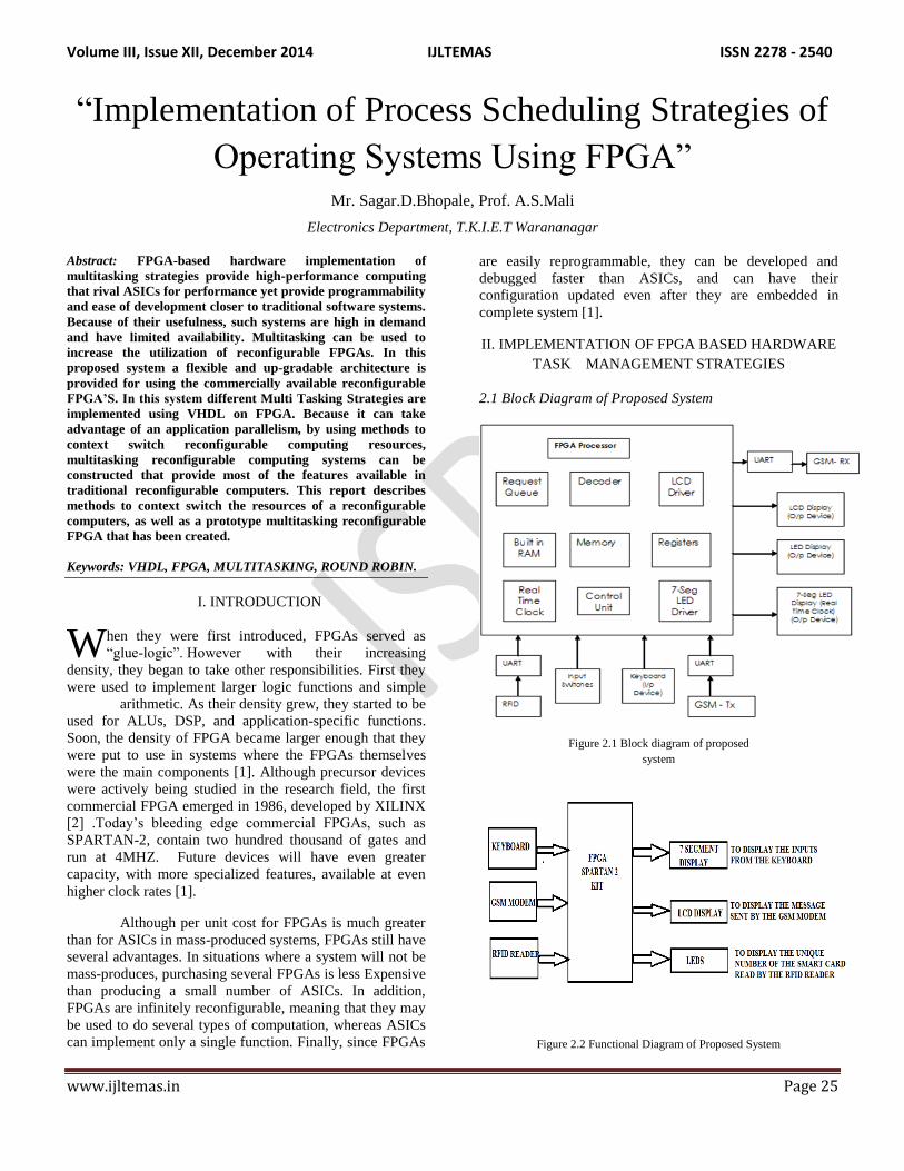
2.1 Block Diagram of Proposed System
Figure 2.1 Block diagram of proposed
system
Figure 2.2 Functional Diagram of Proposed System
W
Volume III, Issue XII, December 2014 IJLTEMAS ISSN 2278 - 2540
www.ijltemas.in Page 26
Working Principle
The hardware tasks (applications), in the functional
diagram run in different modes.
There are three modes namely multitasking,
Round-Robin & request/acknowledgement modes
implemented in this proposed system.
The inputs from the keyboard are displayed on 7-
Segment display interfaced.
The message received from the GSM MODEM is
displayed on LCD display.
The unique identification number of the smart card
is read by the RFID reader and is displayed on
LEDS on the FPGA board.
The different modes of operations are explained in
the section 2.3.
Figure 2.3 RTL Schematic of Hardware Task Management
2.2 Functionality of Modules
2.2.1 GSM Modem
The working of GSM MODEM contains two
sections, UART receiver and the UART transmitter section,
the UART receiver, receives the message from the user
mobile. UART transmitter sends an acknowledgement to the
user mobile.
UART Receiver
The UART Receiver receives the messages sent by
the mobile user. The GSM Modem to read that particular
message AT command is needed, that AT command is
AT+CMGR=loc
Figure 2.4 UART Receiver
The modem is interfaced to FGPA kit through
UART (RS232 cable), The UART receiver on FPGA
module receives the upcoming serial data and converts it
into parallel 8-bit data. In this proposed system the
upcoming data (message) is displayed on the LCD display.
This LCD display is having the capability of displaying 16
characters at a time; it means up to 128 bits (16*8) can be
displayed. For that 8-bit to 128 bit converter is required and
it is implemented in this proposed system.
Figure 2.5 RTL Schematic of the GSM Modem Receiver
This RTL Schematic shows the entire working of
GSM MODEM Receiver section. First baud generator is
taking the available 4 MHz clock of spartan2 FPGA kit and
converting it into 16 clock pulses and which is giving to
UART receiver as clock. Then UART receiver takes serial
data (message) from GSM MODEM through RS232 cable
and converts it into 8-bit parallel data and which is applied
to 8 to 128 converter. The 8 to 128 converter converts the
upcoming 8-bit parallel data into 128 bits and then it is
giving to LCD as input. Then LCD will display the result
(message).
UART Transmitter
The AT command given AT+CMGR=loc is of 11
characters (11*8= 88 bits), A enable generator is used to
convert 88 bits to 8-bit parallel data. UART transmitter
converts 8-bit parallel data to serial data, and then at the end
of this process the user gets the delivery report as
Volume III, Issue XII, December 2014 IJLTEMAS ISSN 2278 - 2540
www.ijltemas.in Page 27
acknowledgement
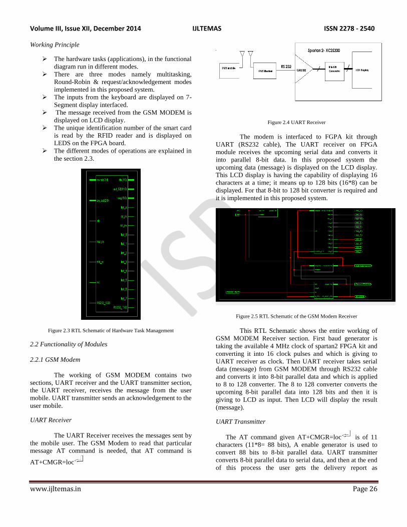
Figure 2.6 GSM MODEM Transmitter Section
Figure 2.7 RTL Schematic GSM Modem Trasmitter
This RTL Schematic shows the entire working of GSM
MODEM Transmitter section. First baud generator is taking
the available 4 MHz clock of spartan2 FPGA kit and
converting it into 16 clock pulses and which is giving to
UART transmitter as clock. Then the transmitter takes the 8
bit parallel data and converts it into serial data then through
this entire process mobile user will get acknowledgement.
2.2.2 RFID Reader
The RFID reader shown in the figure reads the
unique identification number (UIN) of the RFID (Smart
cards) tag, the RFID reader is interfaced to the FPGA
module through UART, the UART receiver on the FPGA
module converts the upcoming serial data into 8-bit parallel
data. The RFID tag is used in this system has the 8 character
UIN (8*8=64 bits), each character has a start bit and a stop
bit, totally 80 bits. Decoder converts the 8-bit data into 80
bits and is displayed on LEDs on the FPGA board.
Figure 2.8 RFID Receiver Section
Figure 2.9 RTL Schematic of the RFID Receive
This RTL Schematic shows the entire working of RFID
Receiver section .First baud generator taking the available 4
MHz clock of spartan2 FPGA kit and converting it into 16
clock pulses and which is giving to UART Receiver as
clock. Then the UART Receiver takes the unique
identification number (UIN) from the RFID Reader through
RS232 cable in a serial way then converts it into 8 bit
parallel data. Then the decoder converts the 8 bit data into
80 bit parallel data. Then the 64 bits data will be given to
LEDs. Then unique identification number of RFID tag will
be displayed on the LEDs on FPGA board.
2.2.3 Keyboard
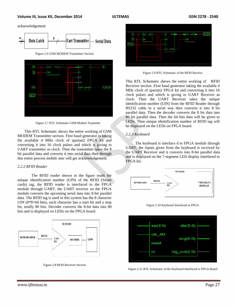
The keyboard is interface d to FPGA module through
UART, the inputs given from the keyboard is received by
the UART Receiver and it converts into 8-bit parallel data
and is displayed on the 7-segment LED display interfaced to
FPGA kit.
Figure 2.10 Keyboard Interfaced to FPGA
Figure 2.11 RTL Schematic of the Keyboard Interfaced to FPGA Board
Volume III, Issue XII, December 2014 IJLTEMAS ISSN 2278 - 2540
www.ijltemas.in Page 28
2.3 Mode Selection
Table 2.1 Mode Selection
MODE SELECTION BITS
MODE SELECTED
001
Multi tasking
010
010 & 001
010 & 010
010 &100
Request/acknowledgement
Keyboard
RFID Reader
GSM Modem
100
Round – Robin
2.3.1 Multitasking Mode
Multitasking is a method for sharing system
resources so that multiple processes can appear to run
simultaneously. Multitasking is a method where multiple
tasks, also known as processes, share common processing
resources such as a XC2SPQ208 processor.
When inputs from the dip switches of the FPGA
board are 001, multitasking mode is selected. In this mode
all the tasks (applications) run simultaneously i.e. the inputs
from the keyboard is displayed on the seven-segment
display, the UNI of the RFID tag which is read by the RFID
reader is displayed on the LEDs of the FPGA board and the
message received by the GSM modem is displayed on the
LCD display of the board.
2.3.2 Request / Acknowledgement Mode
In this mode application (transmitter) to be served
sends a request to the processor before transmitting the data.
And if the resources are free and ready to receive the data
then it sends an acknowledgement signal to the transmitter.
Then the connection between transmitter and receiver will
be established.
When the inputs from the Dip switches of the
FPGA board are 010, request/ acknowledgement mode is
selected.
When inputs are 010 & 001, the keyboard
application is served, the inputs from the keyboard are
displayed on the 7-Segment display, and all other
applications are ignored.
When inputs are 010 & 010, the RFID Reader is
requesting for the service, and it is served, the UNI of the
smart cards which is read by RFID reader is displayed on
the LEDS.
When inputs are 010 & 100, the GSM Modem is
requesting for the service, and it is served, the message
received by the modem is displayed on the LCD display.
2.3.3 Round-Robin Mode
In a round-robin system several processes are executed
sequentially to completion, often in conjunction with a
cyclic executive. In round-robin systems with time slicing,
each executable task is assigned a fixed-time quantum
called a time slice in which to execute. A fixed-rate clock is
used to initiate an interrupt at a rate corresponding to the
time slice. The task executes until it completes or its
execution time expires, as indicated by the clock interrupt.
If the task does not execute to completion, its context must
be saved. The task is the placed at the end of the executable
list. The context of the next executable task in the list is
restored, and it resumes execution. Round-robin systems
can be combined with pre-emptive priority systems,
yielding a kind of mixed system.
In this proposed system a time slice of sixty
seconds is implemented, each tasks run for sixty seconds
later they are preempted. Priority has to be assigned,
keyboard is assigned higher priority, RFID reader second
and GSM modem the lower priority.
When this mode is selected, all the tasks run
sequentially for the assigned time interval based on the
assigned priority.
III. SIMULATION RESULTS
3.1 List of Simulations:
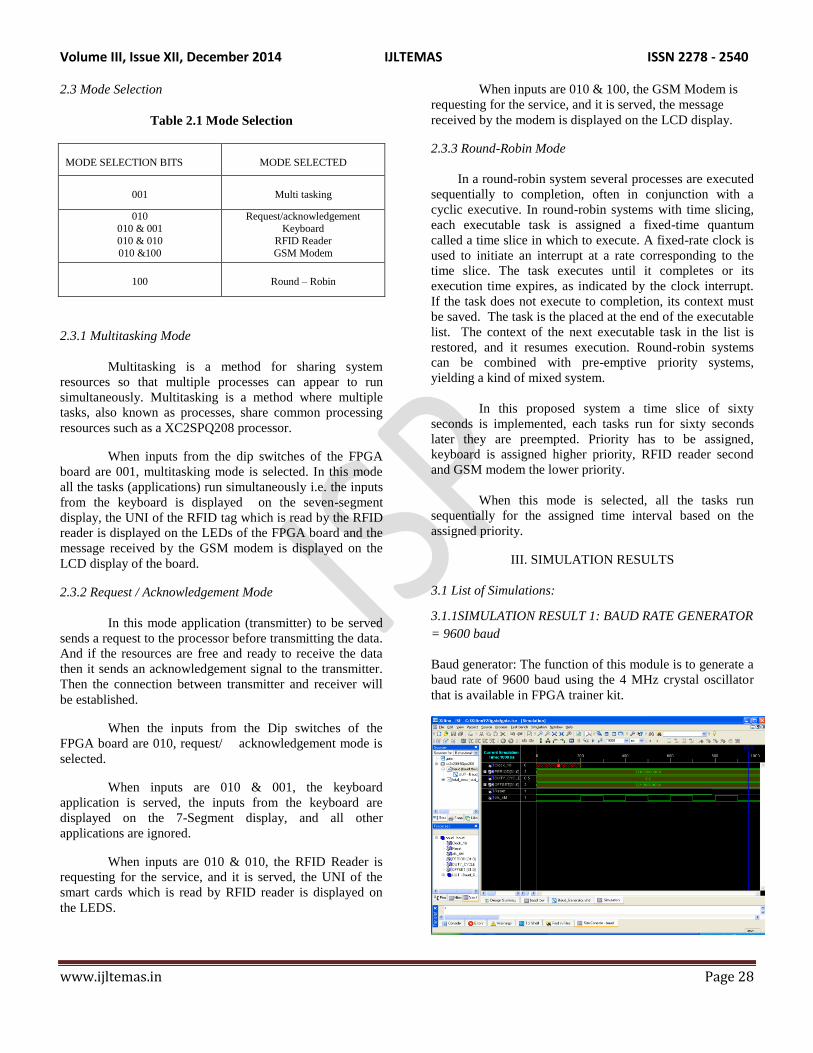
3.1.1SIMULATION RESULT 1: BAUD RATE GENERATOR
= 9600 baud
Baud generator: The function of this module is to generate a
baud rate of 9600 baud using the 4 MHz crystal oscillator
that is available in FPGA trainer kit.
Volume III, Issue XII, December 2014 IJLTEMAS ISSN 2278 - 2540
www.ijltemas.in Page 29
clk_4M: 4 MHz clock signal from FPGA
Reset: is used to reset the process
Clock_16: output clock signal which is 1/16 the
frequency of the inbuilt clock
3.1.2 SIMULATION RESULT 2: DATA LATCH: 88 bit to 8
bit conversion
The function of the Data Latch module is to
convert block of 88 bits and transmit them in blocks of 8
bits to the UART transmitter. This conversion should be
done in synchronisation with the generated baud rate.
Further the enable signal
The AT( attention) commands sent from the FPGA
to GSM modem is in blocks of 88bit. Hence this module
aids in serial transmission via RS232 standards
Data_in: 88 bit input
Dout: 8 bit output
Enable : functions as clock reference for this module
Load : indicates that a block of data is available for
conversion
3.1.3 SIMULATION RESULT 3: DECODER (hexadecimal
to decimal)
This module performs the simple decoding from
hexadecimal to decimal value.
Decoder in: 8 bit hexadecimal input
Decoder out: 8 bit decimal output
3.1.4 SIMULATION RESULT 4: Enable signal generation
This module is to generate an enable signal whenever FPGA
detects an incoming message on the GSM modem. Sms_in:
indication that an message has arrived and is stored in the
GSM modem memory.
Clk_4M: clock signal
3.1.5 SIMULATION RESULT 5: Latch 1 8bit to 128 bit
This module converts 8 bit blocks received from the UART
receiver into 128 bit blocks for compatibility with the 16
character LCD display
3.1.6 SIMULATION RESULT 6: UART RECEIVER
This block synchronizes with the baud rate generator to
generate tick signal once for every 26th
clock cycle of the 4
MHz clock input. This ensures the sampling of the serially
received bits from the receive line (rx) on the UART
receiver.
Volume III, Issue XII, December 2014 IJLTEMAS ISSN 2278 - 2540
www.ijltemas.in Page 30
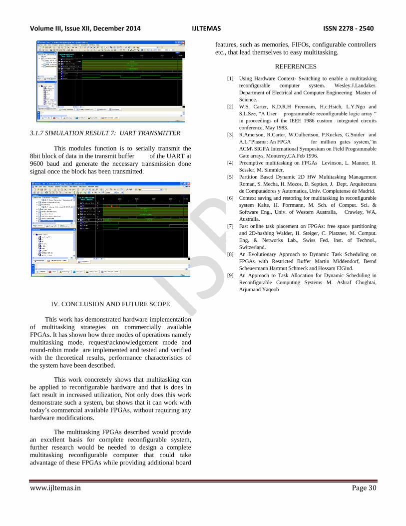
3.1.7 SIMULATION RESULT 7: UART TRANSMITTER
This modules function is to serially transmit the
8bit block of data in the transmit buffer of the UART at
9600 baud and generate the necessary transmission done
signal once the block has been transmitted.
IV. CONCLUSION AND FUTURE SCOPE
This work has demonstrated hardware implementation
of multitasking strategies on commercially available
FPGAs. It has shown how three modes of operations namely
multitasking mode, request\acknowledgement mode and
round-robin mode are implemented and tested and verified
with the theoretical results, performance characteristics of
the system have been described.
This work concretely shows that multitasking can
be applied to reconfigurable hardware and that is does in
fact result in increased utilization, Not only does this work
demonstrate such a system, but shows that it can work with
today’s commercial available FPGAs, without requiring any
hardware modifications.
The multitasking FPGAs described would provide
an excellent basis for complete reconfigurable system,
further research would be needed to design a complete
multitasking reconfigurable computer that could take
advantage of these FPGAs while providing additional board
features, such as memories, FIFOs, configurable controllers
etc., that lead themselves to easy multitasking.
REFERENCES
[1] Using Hardware Context- Switching to enable a multitasking
reconfigurable computer system. Wesley.J.Landaker.
Department of Electrical and Computer Engineering Master of
Science.
[2] W.S. Carter, K.D.R.H Freemam, H.c.Hsich, L.Y.Ngo and
S.L.Sze, “A User programmable reconfigurable logic array “
in proceedings of the IEEE 1986 custom integrated circuits
conference, May 1983.
[3] R.Amerson, R.Carter, W.Culbertson, P.Kuckes, G.Snider and
A.L.”Plasma: An FPGA for million gates system,”in
ACM\ SIGPA International Symposium on Field Programmable
Gate arrays, Monterey,CA.Feb 1996.
[4] Preemptive multitasking on FPGAs Levinson, L. Manner, R.
Sessler, M. Simmler,
[5] Partition Based Dynamic 2D HW Multitasking Management
Roman, S. Mecha, H. Mozos, D. Septien, J. Dept. Arquitectura
de Computadores y Automatica, Univ. Complutense de Madrid.
[6] Context saving and restoring for multitasking in reconfigurable
system Kalte, H. Porrmann, M. Sch. of Comput. Sci. &
Software Eng., Univ. of Western Australia, Crawley, WA,
Australia.
[7] Fast online task placement on FPGAs: free space partitioning
and 2D-hashing Walder, H. Steiger, C. Platzner, M. Comput.
Eng. & Networks Lab., Swiss Fed. Inst. of Technol.,
Switzerland.
[8] An Evolutionary Approach to Dynamic Task Scheduling on
FPGAs with Restricted Buffer Martin Middendorf, Bernd
Scheuermann Hartmut Schmeck and Hossam ElGind.
[9] An Approach to Task Allocation for Dynamic Scheduling in
Reconfigurable Computing Systems M. Ashraf Chughtai,
Arjumand Yaqoob