IIIIIIIIIIIhIl - DTIC
92
AD-A148 293 NONLINEAR REAL-TME OPTICAL SIGNAL PROCESSINO U) UNIVERSITY OF SOUTHERN CALIFORNIA LOS ANGEL ES MAGE PROCESSIN AA SAWCHUK ET AL, 01 OCT 84 USCIPI-1130 UNCLASSIFIED AFOSR- R-84-107 AFOSR-81-0182 F/G 20/6 NL IhIIIIIIIIl-E Elllllllll-E0 ElEEEMAlllI IIIIIIIIIIIhIl llE~llllEllE-
-
Upload
khangminh22 -
Category
Documents
-
view
1 -
download
0
Transcript of IIIIIIIIIIIhIl - DTIC

AD-A148 293 NONLINEAR REAL-TME OPTICAL SIGNAL PROCESSINO U)UNIVERSITY OF SOUTHERN CALIFORNIA LOS ANGEL ES MAGEPROCESSIN AA SAWCHUK ET AL, 01 OCT 84 USCIPI-1130
UNCLASSIFIED AFOSR- R-84-107 AFOSR-81-0182 F/G 20/6 NL
IhIIIIIIIIl-EElllllllll-E0
ElEEEMAlllIIIIIIIIIIIIhIlllE~llllEllE-

IIII1" III 1.0
I 1.8
IIII III1 1 /
U ,
0 7 USCIPI Report 1130
E ~C~,OUTfitA
N Ivj)
UNIVERSITY OF SOUTHERN CALIFORNIA- I FINAL TECHNICAL REPORT
April 15, 1981 - June 30, 1984
N NONLINEAR REAL-TIME OPTICAL SIGNAL PROCESSING
i E~ A.A. Sawchuk, Principal InvestigatorT.C. Strand and A.R. Tanguay. Jr.
October 1, 1984
RDepartment of Electrical Engineering
Image Processing instituteUniversity of Southern California
University Park-MC 0272Los Angeles, California 90089-0272
Research sponsored by theAir Force Office of Scientific Research
Electronics and Materials Science Divisionunder Grant No. AFOSR-81 -0182
DTICELECTE
I B
IIMAGE PROCESSING INSTITUTE
84 11 26 107

UNCLASSIFIED
SECURITY CLASSIFICATION OF THIS PAGE (When Dota Entered),
REPORT DOCUMENTATION PAGE READ INSTRUCTIONSBEFORE COMPLETING FORM
1. R~PRT NUMBER 2. GOVT ACCESSION NO. 3. RECIPIENT'S CATALOG NUMBER
4. TITLE (and Subtitle) 5. TYPE OF REPORT & PERIOD COVEREDFinal Technical Report
NONLINEAR REAL-TIME OPTICAL SIGNAL PROCESSING 4/15/81 to 6/30/846. PERFORMING O1G. REPORT NUMBER
USCIPI Report 11307. AUTHOR(s) 8. CONTRACT OR GRANT NUMBER(s)
A.A. Sawchuk, T.C. Strand, and A.R. Tanguay,Jr. AFOSR-81-0182
9. PERFORMING ORGANIZATION NAME ASID ADDRESS 10. PROGRAM ELEMENT. PROJECT. TASKDepartment of Electrical Enginering AREA & WORK UNIT NUMBERS
Image Processing Institute, MC 0272University of Southern California, LA, CA 90089
II. CONTROLLING OFFICE NAME AND ADDRESS 12. REPORT DATEAir Force Office of Scientific Research October 1, 1984Bldg. 410, Bolling AFB 3. NUMBER OF RAGESWashington, D.C. 20332 86
14. MONITORING AGENCY NAME & ADDRESS(if different from Controlfing Office) IS. SECURITY CLASS. (of this report)
As above Unclassified
15-. DECL ASSI FICATION/'DOWN GRADIN4GSCHEDULE
16. DISTRIBUTION STATEMENT (of this Report)
The t< Sta> o5vbnment orized roduce ja-dstributey rint sfo Glover nyral purp notwithst g any cop rg notatioh eon.
17. DISTRIBUTION STATEMENT (of fhe abstract entered in Block 20, if different from Report)
18. SUPPLEMENTARY NOTES
19. KEY WORDS (Continue on reverse side It necessary and identify by block number)
Optical information processingNonlinear optical processingOptical computingLight valves
20. %9STRACT (Cntinue on reverso side f neceseary and identify by block number)
This report summarizes the results of a research program in nonlinear real-timeoptical signal processing. The program began April 15, 1981 and ended June 30,1984. The research effort has centered on optical sequential logic systemsand their use in digital optical computers, and on variable grating mode (VGM)liquid crystal spatial light modulators. As part of this study, parallel andtwisted nematic liqu.,i, crystal light valve (LCLV) devices have been used as anonlinear element in . feedback arrangement to implement a binary sequential
DD R 1473 EDITION OF I NOV &5 IS OBSOLETE UNCLASSIFIED
SECURITY CLASSIFICATION OF THIS PAGE (When Date Entered)

UNCLASSIFIED
SECURITY CLASSIFICATION OF THIS PAGE(Wh. D&I& Erter.d)
logic system. A computer generated hologram fabricated on an e-beam systemserves as a beamsteering interconnection element. A completely opticaloscillator and frequency divider have been experimentally demonstrated, andvarious circuit interconnection techniques have been explored. Variable-gratingmode (VGM) liquid crystal devices that perform local spatial frequency modulatioras a function of the incident intensity have also been investigated. Thesedevices can be used for nonlinear processing by selection and recombination ofthese spatial frequency components. These devices have many interesting physicaleffects with useful applications in both analog and numerical optical signalprocessing. Results on the physical modeling of VGM devices are given, withparticular ephasis on experimental measurements of the Jones matrix describingpolarized light propagation through the VGM cell. The program was performed witfthe cooperation of the Hughes Research Laboratories of Malibu, Cali-fornia.
D t ltb t oo/
Av tlbl ity Codes
Av-11 nnaior-SI.". ! 'peci!al
U SS
L UNCLASSI FIED

FINAL TECHNICAL REPORT
April 15, 1981 - June 30, 1984
NONLINEAR REAL-TIME OPTICAL SIGNAL PROCESSING
A.A. Sawchuk, Principal Investigator
T.C. Strand and A.R. Tanguay, Jr.
October 1, 1984
Department of Electrical Engineering
Image Processing Institute
University of Southern CaliforniaUniversity Park-MC 0272
Los Angeles, California 90089-0272
Research sponsored by theAir Force Office of Scientific Research
Electronics and Materials Science Division
under Grant No. AFOSR-81-0182
USCIPI Report 1130
The United States Government is authorized to reproduce and distribute reprints for
Governmental purposes notwithstanding any copyright notation hereon.

TABLE OF CONTENTS
Page
ABSTRACT ii
1. RESEARCH OBJECTIVES AND PROGRESS 2
1.1 Introduction and Project Overview 2
1.2 Digital Optical Computing 5
1.3 Variable Grating Mode Liquid Crystal
Devices 59
1.4 References 78
2. PROFESSIONAL PERSONNEL 30
3. PUBLICATIONS 81
4. ORAL PRESENTATIONS AND INTERACTIONS 83
I!

ABSTRACT
This report summarizes the results of a research program in
nonlinear real-time optical signal processing. The program began
April 15, 1981 and ended June 30, 1984. The research effort has
centered on optical sequential logic systems and their use in
digital optical computers, and on variable grating mode (VGM)
liquid crystal spatial light modulators. As part of this study,
parallel and twisted nematic liquid crystal light valve (LCLV)
devices have been used as a nonlinear element in a'feedback
arrangement to implement a binary sequential logic system. A
computer generated hologram fabricated on an e-beam system serves
as a beamsteering interconnection element. A completely optical
oscillator and frequency divider have been experimentally
demonstrated, and various circuit interconnection techniques have
been explored. variable-grating mode (VGM) liquid crystal
devices that perform local spatial frequency modulation as a
function of the incident intensity have also been investigated.
These devices can be used for nonlinear processing by selection
and recombination of these spatial frequency components. These
devices have many interesting physical effects with useful
applications in both analog and numerical optical signal
processing. Results on the physical modeling of VGM devices are
given, with particular emphasis on experimental measurements of
the Jones matrix describing polarized light propagation through
the VGM cell. The program was performed with the cooperation of
the Hughes Research Laboratories of Malibu, California.

1. RESEARCH OBJECTIVES AND PROGRESS
1.1 Introduction and Project Overview
This report summarizes the final results of a research
effort in performing nonlinear operations in optical signal
processing and achieving operation in real time using various
input transducers. The project began April 15, 1981 and ended
June 30, 1984. This section contains an introduction, motivation
for the work and an overview of the research program.
The research described in this report addresses the need for
signal processing systems that can perform high throughput
parallel multi-dimensional operations on signals with large
time-bandwidth and space-bandwidth products. In many of these
applications, digital hardware is inadequate. As part of this
project, modifications have been made to existing liquid crystal
light valve (LCLV) real-time spatial light modulators and new
devices such as the variable grating mode (VGM) light valve have
been developed. Another goal of this research has been to
explore numerical optical computing using binary or residue
arithmetic. in these systems, signals exist as discrete levels
rather than as analog signals. This new approach holds much
promise for the future if real-time processing speed, accuracy,
and flexibility can be maintained.
A book chapter [1] written by research personnel supported
under this grant has been recently completed summarizing the

2
state-of-the-art of all techniques of nonlinear optical
processing. This chapter contains extensive references. Three
major techniques of optically implementing nonlinear point
functions have been developed. They are: halftoning; direct
nonlinear processing using the inherent characteristics of image
detectors and transducers; and intensity-to-spatial frequency
conversion. Application examples and real-time implementation of
these techniques are described in the review papers.
In the research phase summarized in this report we have
concentrated on: optical sequential logic systems that directly
rely on the input-output characteristics of LCLV devices; and on
variable grating mode (VGM) devices and their applications.
Nonlinear optical functions can be achieved directly using
the inherent transfer characteristics of an optical recording
medium or real-time image transducer. With this type of
nonlinear processing, there is no pulse-width modulation,
intensity-to-spatial frequency conversion or other type of
intermediate mechanism. Thus, these techniques offer the
potential of simple systems that avoid the noise problems
associated with many optical filtering techniques and have much
less stringent space-bandwidth product requirements than systems
which must modulate the input data. Such systems can implement
parallel combinatorial logic and, with the addition of feedback,
parallel sequential logic. Section 1.2 of this report describes
recent results on these subjects and work on the general area of

3
digital optical computing.
Another convenient method of obtaining point nonlinearities
is through intensity-to-spatial frequency conversion. The idea
is to encode each resolution element of an image with a grating
structure where the period and/or the orientation of the grating
is a function of the image intensity at the point in question.
Assuming certain sampling requirements are met, each intensity
level of interest is uniquely assigned to a different point :n
Fourier space and all points with a given intensity in the -image
are assigned tu the same point in Fourier space (assuming
space-invariant operation is desired). Then a pure amplitude
spatial filter can alter the relative intensity levels in an
arbitrary way, and combination of the filtered components
produces various nonlinear functions. Both continuous-level
(analog) nonlinear functions and various numerical logic
functions (binary or residue) are possible. This method relies
on the behavior of variable-grating mode (VGM) liquid crystal
real-time devizes which have been developed under this AFOSR
program. Section 1.3 of this report describes work on physical
modeling and measurements of VGM liquid crystal devices. The
goal of this work is to improve their temporal response,
uniformity, lifetime, etc. Several new types of electrically and
optically activated VGM devices have been constructed and
evaluated.
This program has been very productive; a number of oral

4
presentations have been made and many written papers have been
published describing research results. Some of the most
significant of these papers are reprinted as part of this report.
The overall program has been a joint cooperative effort
between the University of Southern California (USC) group and the
Hughes Research Laboratories (HRL) in Malibu, California. Each
group has participated in the project together and a separate
progress report is being submitted by HRL as a comparison to this
report. Both groups haye worked closely together in their
particular areas of expertise toward the project goals.

5
1.2 Digital Optical Computing
1.2.1 Introduction
There has been considerable work in recent years in
developing optical systems that perform essentially digital
processing functions. The reasons for this interest include
extending the flexibili-y of optical processing systems and the
possibility of using the parallel capabilities of optical systems
for digital signal processing. The first steps in this digi
optical computing research have included parallel A/D conversio
and optical combinatorial logic implementation. Both of these
have been demonstrated in real-time systems at USC [11-[3].
The next step in this progression of experiments is to
demonstrate the feasibility of optical sequential logic. Here
the basic logic gates are interconnected in a circuit which
generally includes some form of feedback. In this system the
temporal response characteristics of the system become very
important. We have developed an optical system which
demonstrates the feasibility of optical sequential logic. 1r.
particular we have implemented a totally optical system whicn
includes a clock driving a master-slave flip-flop. The basic
elements of a sequential logic system are a nonlinear element
that performs the desired logic function and an interconnection
system to route the outputs of the nonlinear device to the
appropriate inputs.

6
Four recent papers that contain the details of this work are
reprinted here. The first paper is "Sequential Optical Lgi:
implementation", by B.K. Jenkins, A.A. Sawchuk, T.C. Strand,
R. Forchheimer and B.H. Soffer. This paper recently appearec in
Applied Optics and concentrates on experimental results from -.e
sixteen gate clocked master-slave optical flip-flop.
A second paper "Architectural implications of Digital
Optical Processors" by P. Chavel, R. Forchheimer, B.K. Jenkins,
A.A. Sawchuk and T.C. Strand, has just been published in App!Le
:otics. it describes various interzonnection techniques :cr
optical sequential logic systems, including space-variant,
soace-invariant and hybrid computer-generated holograms.
A third paper, "Computer-Generated Holograms -or
Space-Variant Interconnections in Optical Logic Systems," by
B.K. Jenkins and T.C. Strand was published in SPIE Proceedings
vol. 437 for the international Conference on Computer-Generated
Holography held in August 1983 in San Diego. This paper
describes details of space-variant computer hologram
interconnection schemes for optical logic and computing systems.
Another paper, "Digital Optical Computing," by A.A. SawchuK
and T.C. Strand appeared in the July 1984 Proceedings IEEE
Special Issue on Optical Computing. This paper is a
comprehensive overview of binary combinatorial and sequential
logic with iindividual devices and arrays of devices. The paper
discusses communication, interconnection and input-output

7
problems of digital electronic computers at the gate, chip and
processor level. Some architectural techniques for avoiding some
of the interconnection problems of electronic VLSI are presented.
The possibi:ity of non Von Neumann parallel digital processors,
.mitatlons and future needs of optical logic devices and digital
-~7 :zmpu:_ng systems are discussed.

8
Sequential optical logic implementation
B. K. Jenkins, A. A. Sawchuk, T. C. Strand, R. Forchheimer, and B. H. Softer
An optical svstem that performs sequential binary logic operations is described. 1I'he .sstcm cvuss i aspatial light modulator iSNLM) used to provide a nonlinear thresh,,ld response and a coiiputer-.,ner;Itedhologram to pro ide interconnections between logic gates. A 2-D array of logic gates with binary mpuit. .doutputs is formed ,n the active surface of the SLM. 'These gates are intercoinected by a 2- D array, t"subho-
lugrams. one for each gate. Arbitrary logic circuits consisting ,f NOR gates and inverters can be imple:i.rnt-cd. and the system can Ive reconfigured by changing a single holographic elemenL The sytem .s demon-strated using a twited-nematic liquid crystal light valve as the SLM. A test circuit is implemented that n-
cludes a synchronous master-slave flip-tlop and an oscillator consisting of five inverters in a feeciback (!.op.Experimental results of this test circuit are presented.
I. Introduction dimensional arrays of some of these operations such as
The vast majority of optical processing systems to OR, NOR, AND, NAND, XOR, and XNOR have beindate have iperated with analog signal levels. While demonstrated using a variety of optically addressrd 2-Dmaiy of these .ystems can perform specific operations spatial light modulators kSLMs). These include !hewith extremely high throughput rates, at the same time Pockels readout optical modulator (PROM), ' .9 thethey suffer from two basic limitations: the variety of microchannel spatial light modulator (MSLM), ri-l : theoperations that can be performed and the accuracy of Hughes liquid crystal light valve (LCLV),12-14 and athe results. These limitations preclude the use of op- segmented liquid crystal light valve used as an optica:ticad processing systems in certain application areas that parallel logic (OPAL) device.' 5" 6 These operaTionscould otherwise benefit from some of the inherent ad- have also been demonstrated using light-emittingvantages of optics. These advantages include a high diodes with optical masks.' 7 Other schemes, too nu-degree of parallelism, both in processing and input/ merous to mention, have also been used to implementoutput, and a high density and number of intercon- logic gates optically. A review of optical computingnections. Two approaches have beentaken to eliminate systems, including these combinatorial operations, isor at least substantially reduce these limitations. Both given in Ref. 18. Recently, individual all-optical logicapproaches utilize discrete, instead of analog, signal gates have been demonstrated in InSb (Ref. 19) andlevels. One approach is based on residue arithmetic GaAs. 20
operations, and optical systems utilizing this principle Although these operations form the basic buildinghave been studied.1- 7 The other approach is based or blocks for combinatorial logic, to build a sequentiaibinary logic operations, such as used in conventional circuit or an optical computer, memory is also needed.electronic computers. This can be achieved using optical feedback. An array
The first step in the binary approach has been to of optical flip-flops has been demonstrated using andemonstrate Boolean operations optically. Two- LCLV in an optical system with feedback, 21.2 2 and an
array of optical latches has been demonstrated by usingan OPAL device with optical feedback. 23 Fast indi-vidual bistable elements have also been demonstratedin many materials using feedback by means of aFabry-Perot cavity. 24
B. H. Soffer is with Hughes Re.earch Laboratories. Malibu, Cali- These elements, however, have not been combinedfornia 90265. 'Nhen this work was done the other authors were with to form an all-optical logic circuit. Such a circuit mayUniversity of Southern California, Department of Electrical Engi- have the potential of combining the high degree ofneering. Los Ang'les, California 90089; T. C. Strand is now with IBMCorp., San Jose, California 95193 and R. Forchheimer is now with parallelism and interconnection density found in opticalLinkoping University, Linkoping, Sweden. processors with the flexibility and accuracy of digital
Received 6 January 1984. electronic computers. A method for combining these0003-6935/84/193455-10$02.00/0. binary elements using fiber optics has been described ,2
, 19F4 Optical Society of America. but a complete system has not been demonstrated ex-
1 October 1984 / Vol. 23. No. 19 / APPLIED OPTICS 3455

9perimentally. Other digital optical processing systems 0,OR2 - - B
have also been described. 6. 7 A system with an array --o. ,,)f optical gates and some optical memories, underelectronic control, has been demonstrated.28 Thissystem is particularly useful for operations requiring INPUT 2
only local communication, as is the case for many image Fig. 1. Implementation ofa logic gate.processing operations, e.g., cellular logic machines.
In this paper a system is presented which intercon- INPUT
nects optical logic elements to form a sequential logic INPUT 2circuit. Every signal in this system is represented op- 0,...,oR N B , INT.AR ,tically, and at the same time the system permits im- N
plementation of arbitrary connections between the in- INPUT Ndividual logic gates. Because this system is digital, the BINARYINPUT
accuracy limitation mentioned above can be overcome LINESby selecting the number of bits per data element to yield Fig. 2. Generalization of Fig. I to N-input gates.the desired accuracy. In addition, the arbitrary inter-connections of the system presented here permit im-plementation of a very large variety of processing op- OuTl
erations. Finally, the advantages of parallelism and Po0 T
interconnection density are retained to a large de- ogree. 29 101
In the system presented here, an SLM is used as a 2-D ouT OUTarray of independently acting logic gates. These gates NANO I.
are interconnected via an optical system that utilizes a o o 2 I ....computer-generated hologram. In this paper we dis- O 'cuss the SLM implementation of logic gates in Sec. II, OR h
the interconnection system in Sec. III, and some ex- o- ...perimental results of the implementation of a test cir- , 2 IN ,cuit to demonstrate the feasibility of the optical logic ousystem in Secs. IV and V. Finally, in Sec. VI we point ENOR ch Fout some of the fundamental limitations involved in , C)using optical devices as arrays of logic gates and discussthe relevance of these limitations to the system pre- Fig. 3. Nonlinearities for implementation of logic operations: (a)sented here. one-input gates; (b) two-input gates; (c) N-imput gates. (N is as-sumed to be even in the XNOR case.)II. Logic Gates
Binary logic gates may be implemented optically Possible choices of the nonlinear functions for somethrough the use of a point nonlinearity. The general of the common logic operations are shown in Fig. 3. Inscheme used for each gate in our system is depicted in the case of two-input gates, there are a total of sixteenFig. 1. First, the two binary input lines to the gate are possible operations. The operations AND, NAND, OR,added to yield a single three-level signal. The value of NOR, XOR, XNOR, TRUE, and FALSE may be im-this three-level signal [or (N + 1) - level signal for the plemented with this scheme directly [Table l(a)]. Thecase of N-input gates] is then equal to the number of remaining logic functions require the ability to distin-input lines that are true (i.e., that have a value of 1). guish between the two input lines A and B. These op-This signal is then operated on by a nonlinear function erations are A, B, A, B, A B, A. B, A + B, and .4 + B.with a binary-valued output. As will be shown below, These operations can be implemented with a single gateany logic operation can be performed in this manner by by doubling the signal level of one of the input lines, say,choosing the appropriate nonlinear function. Figure A [Table l(b)]; this is conceptually equivalent lo using2 shows the extension of this method to N-input gates. a three-input gate with A going into two of the inputTo implement this scheme optically, the binary values lir..s.are represented by intensity levels with a high intensity However, several subsets of the operations which arelevel representing a 1 and a low intensity level repre- realizable with a single gate form logically complete sets,senting a 0. The addition is done merely by optically obviating the need for these asymmetric functions. Forsuperimposing the input line signals. With a detector example, all logic operations can he built out of NORthat integrates the signal over the input spot, this has gates.the effect of adding the intensity levels regardless of the The nonlinearity required for optical logic may becoherence properties of the light (see Sec. II1). In this implemented with any of a variety of optical devices.paper, the term gate input will refer to this superim- Fast switching times (< l nsec) m:ty be obtained byposed signal (i.e., the input to the nonlinearity), and the using a bistable optical device.u . .2 I.3o This proJ.pectterm input lines will refer to the binary inputs before is discussed in Sec. VI. While in principle these devicessuperposition. can be built as 2-D spatial light modilators, at present
3456 APPLIED OPTICS / Vol. 23. No. 19 / 1 October 1984

1q
10Table I. Desired Vaiues of the Nonflniaity tog the 16 Possibt Logic Opevatlons oi Two Bimny Inputs
Input (atelines input Outputs
A B i.1 + B) AND NAND OR NOR XOR XNOR TRUE FALSE
0 1 1 1 1 0 1 0 1 01 0 1 i 1 1 0 1 0 1 01 1 2 I 0 1 0 0 1 I 0
(a)Input (atelines input OutputsA B (2.4 + B) A B A -l A1 - B A + '+ B00 0 0 0 1 0 0 1 10 1 1 0 1 1 0 0 1 0 11 0 2 1 0 0 1 1 0 1 01 1 3 1 1 0 0 0 0 1 1
(b)
Note: Also listed are the gate inputs. The inputs to the adder are A and B in (a) and are 2A andB in (b).
they are not available. Other optically addressed SLMs (OUTPUTare presently available. While their characteristicallyslow response times may appear to he a major drawback,they provide a practical means for demonstrating thesystem concept. The same sequential optical logicsystem described and demonstrated here may be usedwith other SLMs, including much faster ones, so longas they can provide a suitable nonlinearity, and satisfythe following requirements. First, the inputs andoutputs of the gates must be the same wavelength. Thiseliminates such devices as the PROM, 9 with which the INPUT, 0 0 I__1
write illumination must be a different wavelength than INPUT 2 0 1 0 1
the read illumination. Second, we assume the device Fig. 4. LCLV imput-output characteristic used to impement thehas no memory, although in some cases devices with NOR operation, expressed as a function of relative writing and reading
memory could also be used. Finally, we assume here intensities. (Physical units are omitted for clarity.) The 0 and Ithat the gate inputs and outputs appear on opposite labels denote signal levels corresponding to various binary logicthatthegat inpts nd utpus apea on ppoitelevels.sides of the SLM, although it is worth noting that witha slight rearrangement of the system components, SLMswith gate inputs and outputs on the same side can also The input/output characteristic of an SLM, whenbe accommodated, used in this system, essentially serves as an approxi-
Given these requirements, there are still a variety of mation to the corresponding ideal nonlinearity (e.g., Fig.SLMs that can be used. The microchannel spatial light 3). An important criterion in determining whether amodulator" could be used in this system, as could particular nonlinearity is a sufficiently accurate ap-various types of LCLV.12-14 For the demonstration of proximation is the regeneration or restandardizationthe system presented in this paper, a Hughes LCLV was of the signal level at each pass through a gate. Theused. An LCLV with liquid crystal molecules exhib- general requirement is that a signal should not degen-iting a uniform parallel alignment in the off state may erate in passing through a large number of gates in se-be used to implement nonmonotonic nonlinearities, ries. Assuming a transition time of zero, the signal levelwhich are needed for such operations as XOR.14 In this at each pass through a gate may be read off the SLMsystem, NOR gates were used, and LCLVs with liquid input/output curve. If f(x) represents this curve andcrystal molecules in a variety of configurations can x is the signal level at the gate input, for the case of aprovide the appropriate nonlinearity. For example, simple inverter, the following requirement ensures thatFig. 4 shows the steady-state response for an LCLV with the signal will not degenerate (Fig. 5):a twisted nematic liquid crystal layer biased to imple-ment the NOR operation. The horizontal and vertical at-, <kf(z) <b1 -, for all r(a,,b,), i =01,
axes in Fig. 4, respectively, represent relative writing where k is the gain from the output of one gate to theand reading inten, ities, and these quantities are non- input of the next, and a < x < bi defines the range ofnegative. For clarity, physical units are omitted in Fig. gate input signal levels interpreted as the discrete level4. The 0 and I labels on the axes of Fig. 4 denote writ- i. Thus a gate input xo0(a I,bl) will have an output Yoing and reading signal levels corresponding to various -(xo) in the shaded region, and the input to the nextbinary logic levels. gate will be x1 ,= ky on the x axis and in the shaded
I October 1984 / Vol. 23, No. 19 / APPLIED OPTICS 3457

INPUT
INA(.jr
1
ARRAY LE L'AIGATE OUTPUITS HOLOGRAM OUTF-JT
7 Fig. 6. System schematic for interconnecting gateb. Each pixel of0 i, 60 0O b, the input and output arrays corresponds to a gate. The input array*- 0- 1 is the SLM output (gate output array), and the output array is the
Fig. 5. Gate output y vs gate output x for an inverter that satisfies SLM input (gate input array). In general the hologram producesthe regeneration criterion. The shaded region shows the criterion multiple diffraction orders, only one of which is used. (The rays
for a I input and a 0 output. shown in this perspective sketch are a general indication of the pathof propagation and are distorted for clarity. They should not he n-
region. The above requirement states that, will be terpreted as an exact indication of ray paths.)interpreted as an input level of 0, i.e., that xle(ao,bo).This can be generalized to include the other Boolean the fiber optic assembly. The holographic elementoperations by defining output intervals as the (union consists of an array of subholograms in a one-to-oneof the) mapping through f of the corresponding gate correspondence with the gates or pixels of the inputinput intervals. One then requires appropriate corn- array. The interconnection system is shown sche-binations of output intervals (i.e., all possible sums of matically in Fig. 6. This is only one of several holo-the elements) to map into the corresponding gate input graphic systems that could be used to interconnect the
*intervals. The input/output curve of the LCLV used gates.29 In this system, the input array is imaged ontoin the axperiment does satisfy these criteria for the NOR the subhologram array. The hologram is encoded in theand NOT operations. Fourier domain. A Fourier transform is then taken
optically to obtain the output array. Each subhologramIll. Interconnections reconstructs a set of dots, one dot for each connection
The previous section dealt with optical implemen- to a pixel of the output array. Because of the Fouriertation of logic gates, and in this section we address the transform relationship, the coherence area of the illu-problem of interconnecting these gates optically. The mination at the hologram must be larger than or equalgeneral problem is to be able to implement an arbitrary to the subhologram size. If the coherence area is muchconnection pattern between gate outputs and gate in- larger, fringe patterns will appear in each pixel in theputs. Since gate outputs correspond to inputs of the reconstruction plane. This occurs when differentinterconnection system and outputs of the intercon- subholograms, whose separation is less than the co-nection system become gate inputs, for the remainder herence area, reconstruct dots at the same location inof this section the words input and output will refer to the output array. Spatial averaging over each elementthe interconnection system unless explicitly stated in the output array then results in an effective intensityotherwise. summation, as desired for gate inputs (Yis. I anl 2).
In direct analogy to the use of wires in an electrical Obviously, there must be at leact one complete fringecircuit, optical fibers could be used for the intercon- cycle within the reconstructed pixel area for spatialnections. Although the idea is simple when there is a average to be indicative of the sum of intensities. Thisone-to-one correspondence between inputs and outputs, will be the case so long as the subholograms do notthe method is less obvious when there is not. A possible overlap; defining the pixel area as the area of the mainscheme is described here. Assuming each input illu- lobe of the reconstructed dot, it will include at least twominates enough fibers, the fibers that are illuminated fringe cycles. (The number of fringes per reconstructedby an input j that addresses more than one output can pixel depends on the spacing of the contributing sub-be split so thai an equal number of fibers P, go to each holograms relative to the subhologram size but is in-output. Since all outputs may not have the same dependent of uniform scaling factors, lens focal lengths.,number of fibers, a mask is needed at the input plane and propagation distances.)with an intensity transmittance at each input that is This interconnection system is essentially a space-inversely proportional to Ps. Alternatively, the same variant filter providing a different point-spread function(albeit small, perhaps) number of fibers could be used for each input pixel. Because of the Fourier transformto address all outputs making P independent of j. The relationship, each subho!ogram stores the absoluteproblem of fabricating fiber optic bundles for large ar- position of the output pixels it addresses. This absolutebitrary interconnection patterns, however, is a serious addressing scheme implies that the system does notdrawback unless one has an automated system to do distinguish between global and local interconnectionsso. but discriminates only (n the basis of the position of the
The interconnections in the system presented here output array pixels relative toi the origin of the (utputare implemented with a holographic element instead of array.
3458 APPLIED OPTICS / Vol. 23, No. 19 / 1 October 1984
... .. . dJ

12
To avoid a manufacturing problem similar to that ofthe fiber optic system, the hologram can be recordedopltically using an automated system under computercont rol :" 2 or can be generated entirely by computer.In this experiment the hologram was generated bycomputer. Many types of computer-generated Fou-rier-transform hologram have been demonstrated, :'; andmany of them would suffice for this application. Todemonstrate the operation of the sequential logic sys-tem we used a binary version of the hologram proposedby Lee in 1971Y"- for reasons of simplicity, diffraction 0 lA
efficiency, and SNR in the reconstruction. ' Becauseof the coding process used in the hologram, the desired Fig. 7. Steady-state output 's input relationship frr LCLV used to
oututarry pparsinth (10)difratedodri h implement the NOR operation in the experimental systemn.output array appears in the (1,0) diffracted order in the imlenthNOoprininhexpienlsye.
reconstruction plane leaving the spatially inverted(-1,0) order available for probing the system.
The effect of the hologram on the input array may berepresented by the matrix equation
o=mI. (2) F...... ',I T
Here I is a vector representing the 2-D input array, T F.
lexicographically ordered. This input array is actuallythe gate output array augmented by the system inputs.Similarly, 0 is a vector representing the lexicographi- -- l- __
cally ordered output array (which is the gate input array d
augmented by the systein outputs). Each element of Fig.8. Resolution cell of the 1970 Lee cumputer-generated hlugranthe vector I is binary valued and represents the signal with binary-valued transmittance. Usually d = d'.of the corresponaing pixel in the input array. Eachelement of 0 is a non-negative integer representing thesignal leve4 of the corresponding output array pixel. valve is read out between crossed polarizers and is hi-This integer is between 0 and N if the output pixel ased to implement a NOR operation. Its steady-staterepresents a gate with N input lines and is binary if the input/output relationship is shown in Fig. 7. This re-output pixel represents a system output. M is a matrix sponse, together with the attenuation of the intercon-representation of the interconnect pattern-each ma- nection system, satisfies the regeneration criteria statedtrix element mi is nonzero if and only if there is a con- in Sec. II.nection between pixel j of the input array and pixel i of The gates are interconnected with a binary versionthe output array, mflj is an integer equal to the signal of the Lee (1970) computer-generated hologram.34 inlevel created at output pixel i due to a signal level of 1 a Lee hologram, each complex-valued sample is de-at input pixel j. scribed by a linear combination of four real non-nega-
Using this notation, the fan-in to gate i (or number tive numbers (x1,x2,x3,x4), i.e., is decomposed into itsof input lines to gate i) is equal to the sum of the ele- components along each of the four half-axes in thements in row i of M. The fan-out of gate j (or number complex plane. Each cell of the hologram is dividedof gate input lines, plus the number of system outputs, into four subceJls, one subcel] for each of these fourthat come from the output of gate j) is equal to the sum components. One complex-valued sample is taken atof the elements in column i of M. The fan-out is lim- the center of each subcell. Stored in each subcell is theited only by such parameters as the power of the illu- corresponding component xk of its complex-valuedmination source, hologram efficiency, and SLM input sample. Because of the locations of these subcells, uponsensitivity. The maximum fan-in is a function of the taking the optical Fourier transform, these four com-SLM intensity input/output characteristic. ponents are added with the correct phases to obtain the
With this interconnection technique, the hologram, reconstruction in the (1,0) diffracted order. If theor equivalently the elements of M, completely defines transmittance of the hologram is binary valued, eachthe circuit. Within the limit of the number of gates and subcell actually contains a rectangle whose width isthe maximum power available, any operation that can equal to the subcell width and whose height Fk is pro-be represented by a digital circuit can be implemented portional to the value of the corresponding sampleoptically with this system by encoding the appropriate component xk (Fig. 8).interconnection pattern into the hologram. For the hologram used in this experiment, the
transmittance is binary valued and these values areIV. Experimental Demonstration represented by different optical path lengths, i.e., a
For the experimental demonstration of this system, phase hologram. If the optical path lengths differ byan LCLV with liquid crystal molecules in a 458 twisted a phase of 7r, the theoretical efficiency of the hologramnematic configuration was used as the SLM. The light is four times that of the equivalent absorption holo-
1 October 1984 / Vol. 23, No. 19 / APPLIED OPTICS 3459

'.3
gram.3 3 A possible trade-off is that the (0,0)-order in- 1
tensity may increase by more than a factor of 4. , . "The hologram was written onto photoresist via elec-
tron-beam lithography. Surface relief of the photo-resist provides the optical path length difference in the ,hologram. The electron-beam machine used has a stepsize of 0.125 tAm and has written patterns with line-widths as small as 0.5 ,m. It writes 1.024- X 1.024-mmfields and can stitch them together to cover a maximum - -
area of 102 X 102 mm. The machine provides a far .. ,greater space-bandwidth product than was needed for . ,our test circuit.... . ."--
Our test circuit comprises 16 gates so the hologram 4X
comprises 16 subholograms, which are laid out in a 4×4 array. Each subhologram covers a circular area andhas a diameter of -1.04 mm. Each cell is a square 62.5 (a)gm on a side, and there are 17 cells (68 subcells) alongthe horizontal diameter of each subhologram. Eachsubcell has a width of -15.6 ;4m, or 125 steps of theelectron-beam system, and has a height of 500 steps; 7!. - I
both dimensions have more steps than were needed; 251 - '-z "quantization levels were used for each subcell sample, . 5..-..
keeping the apertures centered in each subcell. "' " "Figure 9 shows pictures of one subhologram taken
with a scanning electron microscope. Figure 9(a) shows 4- ', . "- -nearly the entire subhologram. The rectangles are pits,the exteriors of which are photoresist, and the interiorsof which are just glass substrate. Figure 9(b) shows aclose-up of the top edges of two rectangles. The rec- . ...
tangle interiors (no photoresist) are located below these . - . -edges. The thickness of the photoresist is 1.25 um, and -. - - ..the edges are inclined at -32O with respect to the sub-strate normal. The pictures reveal that the photoresistis slightly rough near the edges but otherwise quite 1)
smooth (except for an occasional defect). Defects are Fig. 9. Scanning electmn microcpe pictures of the interconnection
apparent on the glass but are too small to affect the hologram.
optical quality. Linewidths down to -1 gm were ob-tained.
Defining efficiency as the power in the desired re- erture appropriately and filtering out its diffractionconstruction pixels due to one subhologram divided by effects spatially. This leaves the encoding process asthe power incident on that subhologram, the maximum the major source of noise. The effect of the encodingefficiency over all subholograms was measured to be 5%. process on noise is discussed in Refs. 35 and 36. For theThe other subholograms were intentionally generated case of an interconnection hologram, we can define theto have lower efficiencies to normalize the intensities SNR in each reconstruction pixel as the ratio of thein the reconstruction plane. This measurement was power in the reconstruction pixel when it represents ataken using an illumination wavelength of 514.5 nm, the maximum signal level to the maximum power in thewavelength used in the sequential logic system. This same reconstruction pixel when it represent, a signalis close to the optimum wavelength for this hologram, level of 0. Measurements on our test hologram indicateAside from efficiency, we must consider the noise ap- a typical SNR of -60.pearing in the desired reconstruction order, of which A diagram of the main components of the sequentialthere are three sources: (1) the encoding process used logic system is shown in Fig. 10. An expanded Ar laserto represent the complex-valued function on the holo- beam is incident on the readout side of the LCLV (gategram; (2) scattering from the photoresist and glass output plane). It is reflected off the internal mirror ofsubstrate; and (3) the tail of the (0,0) order. The pic- the LCLV and is imaged from the liquid crystal (gatetures of Fig. 9 indicate that the contribution due to output) plane to the hologram via L 2 . The liquidscattering should be small, and this is verified by ex- crystal plane is situated between crossed polarizers.periment. The effect of the (0,0) order could be sub- The Fourier transform of the field transmit ted by thestantial with some phase computer-generated holo- hologram appears at the write side of the L('LV (gategrams. This effect can be prevented by an appropriate input plane) via LI. The phase of the illumination atchoice of the hologram encoding method or can be the gate input plane is not correct, hut only the intensityremedied by choosing the location of the limiting ap- is of interest. Note that the Fourier transfM rm rela-
3460 APPLIED OPTICS / Vol. 23. No. 19 /I Oclober 1984

14
I. . . .... i r
,ULOG A I 1 I I (2.0)(I,-1) ( , ) ,I
L, / 131416 15 (h-_2
G ATE Alt, 'NP T POLARIER 10 5
A AY ARRAY (0,-I) (,) < 0 .-,-
S1 2 6 +10,2) 01)
-1 CVLr E LASER12 90.) .) (3 *Di~rOAC1iON 1OR RS(0,2 (2,2 1
Fig. 10. Experimental system. Lens L-2 images from the LCLV gate (0) (2 0,) (0,) (-2,.1
output plane (liquid crystal plane) to the hologram plane. Lens L3 1 (10) (0,)
provides a Fourier transform from the hologram plane to the LC'.V - xgate input plane. The hologram comprises an array ofsubhologramo. Fig. 12. (a) Layout of test-circuit gates on the hologram. i b) In-
terconnection patterns stored in each subhohlogram. Each ordered
pair represents the relative r ond y ci)rdinates of a pixel, ,r gateinput, that is addressed.
without feedback. A test circuit was chosen that in-cludes both classes of circuit (Fig. 11), and a hologramwith the appropriate interconnection pattern was gen-erated (Fig. 12). The test circuit includes a synchro-nous master-slave flip-flop and a driving clock. The
c, I.c12 clock circuit is a ring oscillator consisting of an odd
10.., 2 number of inverters. Clock circuits with three gates-2 and with five gates have been implemented. The flip-
3 flop functions as a frequency divider and outputs asignal whose frequency is half of that of the clock and
0 3' whose duty cycle is close to 50%. The outputs of some
- _JUL of the gates in the test circuit are shown in Figs. 13 and14. A discussion of them follows.
Fig. 11. Test circuit consisting of a synchronous master-slave flip-flop with driving clock. V. Discussion of Results
The clock circuit, consisting of five gates in a feedbacktionship provides for complete regeneration of spot lo- loop, will be considered first. The phase delay of thecation during each pass through the feedback loop. In signal in passing through one gate is expected to be 180 °
addition, since the subholograms are not contiguous, a (for inverting gates) plus an additional 360 + 72°n, nmask is effectively incorporated into the hologram. - integer, to insure that the total delay through all fiveThis provides regeneration of the size and shape of each gates is a multiple of 3600. The phase delay in passingpixel and also facilitates alignment, through gate 12 is measured to be 216 ° (Fig. 13) within
A diffuser is placed just in front of the LCLV gate experimental error. An oscillator has also been con-input plane to average over the fringe patterns men- structed out of three gates, in which case the expectedtioned in Sec. IM. This is not necessary when the pixels phase delay through each is 2400 + 120*n, and wasare small enough for the fringe patterns to be beyond measured to be close to 2400. Although nonuniformi-the resolution limit of the device. Since a Lee phase ties across the spatial extent of the LCLV caused vari-hologram was used, and the effects of the (0,0) diffracted ations in characteristics from one gate to anotherorder were of concern, an aperture was used as a spatial yielding a slightly different phase delay through eachfilter at P, to filter out diffraction effects from the lim- gate, the sum of the three phase delays was 720' toiting aperture. This spatial filtering could be obviated within the accuracy of the measurement, as expected.by using a hologram encoding method that puts less The frequency of oscillation of the clock circuit canpower into the (0,0) order (e.g., Hseuh-Sawchuk holo- be changed by changing the number of gates in thegram3 7). The (-1,0) diffracted order in the hologram feedback loop. The five-gate clock circuit oscillated atreconstruction can be used to monitor the gate inputs a frequency of 2.64 ± 0.07 Hz (measurement error).during system operation. The gate outputs can also be (Speed is device-dependent and is discussed in Sees. IIprobed by using a reflection off of the analyzer or the and VI.) If we assume the temporal behavior of thehologram. LCLV can be modeled by a simple RC circuit (consist-
For purposes of demons' ation, a test circuit was se- ing of a series resistor followed by a shunt capacitor),lected. A gate may be used in a circuit with feedback, this measurement implies that the three-gate cl cke.g. to achieve oscillation or memory, or in a circuit should oscillate at a frequency of 6.32 Hz. We observed
I October 1984 / Vol. 23, No. 19 / APPLIED OPTICS 3461

15
INPUT were expected to be the same. This is a result of un-I\J.I,..kx Ix.. equal interconnection losses among different gates in
the clock circuit, due to an error in the hologram, whichcaused gate 11 to output larger pulse widths than gateOUTPUT 12.
OUTPUT VI. Device Limitations
- We have mentioned in Sec. II the possibility of using200 msec much faster devices in place of the LCLV, for example,
- b- 00an optical bistable device. We must consider the fun-Fig. 13. Input and output of one of the five gates in the clock circuit damental potentials and limitations involved in using(gate 12). Each trace represents intensity vs time. The period is b, such devices as optical logic gates, as wel as how they
and the phase delay is 360*. a/b. might comapre with their electrical counterparts. Anumber of people have studied this subject.39
A very important consideration is power dissipation12 of these devices. This takes the form of heat which
must be removed from the device to keep its tempera-ture within operating bounds. Earlier works have in-dicated that optical logic gates may suffer from a higher
! _ J . power dissipation than electronic gates and in particularnoted the unfavorable trend on fundamental limits inoptical logic of increasing power dissipation with de-creasing delay time vs a fundamental limit of power
3 1 _2 7 dissipation that is independent of delay time in the caseof semiconductor electronic devices.4 041 More recentlyit has become evident that most of the power dissipation
4 in a practical integrated circuit is due to the on-chipL.._4 I _+ Iinterconnections instead of the transistors themselves
and that the lower limit on this power dissipation alsoincreases with decreasing delay time. 44 This limit is
1 5 f essentially the same, when plotted on a power vs delaytime graph, as the lower limit on power of an opticalswitching device using an absorptive nonlinearity given200 Tlsec in Ref. 45. Furthermore, the limit on power in the case
Fig. 14. Test circuit outputs, of an optical switch using a reactive nonlinearity in-creases more slowly (than the optical absorptive andelectrical cases) with decreasing delay, although its
6.40 : 0.12 Hz. No attempt to measure the frequency power level is higher in the region of common delaystability was made. The system did, however, sustain times (>1 psec). While lowering the operating tem-oscillations for periods lasting 8 h. (The system was perature of semiconductor logic will lower its powerturned off after 8 h.) Given the number of gates in the dissipation limit to a point," use of an optical resonatorclock circuit, the frequency of oscillation is determined can, in some cases, reduce the limits on the power dis-solely by the temporal characteristics of the LCLV. For sipation of the optical switch.4'5 Finally, we point outsufficiently fast SLMs, the optical path length of the that in the optical case much of the power can poten-interconnection system will also hav an effect. tially be dissipated external to the device, permitting
Measurements we have taken indicate that the LCLV the operation of switches at significantly higher powerresponse time is limited by the photoconductor and that levels than would otherwise be possible.the response time of the liquid crystal is much faster.4 While these fundamental limits on optical switchesImprovements in LCLV photoconductor response can be approached with known materials, ,̂ significanttimes 'a8 should yield higher clock frequencies. Use of prngress, some of a relatively fundamental nature, willoptical bistable devices could improve clock frequencies have to be made for these switching devices to becomeby many orders of magnitude (see Sees. I1 and VI). competitive with electronics..5.46 Optical gates will
The test circuit (which has five gates in its clock cir. probably not replace electronic gates for use in gen-cuit) functions correctly. The output waveforms (Figs. eral-purpose computers in the near future, but their use13 and 14) are not expected to be square. The gates are in an optical special-purpose computer could permitoperating near their maximum speed, so their rise and realization of a number of architectural advantages overfall times are substantial in comparison with their pulse semiconductor electronics.29 These advantages includewidths. With one minor exception, all gates in the test parallel input/output, global as well as local intercon-circuit output the expected waveforms. The exception nections, and implementation of interconnection-in-is that the pulse widths of the outputs of gates 5 and 6 tensive circuits and processors without reducing theare less than those of the outputs of gates 1 and 2. They active device area available for gates.
3462 APPLIFD OPTICS / Vol. 23. No 19 / I October 1984
16
VII. Conclusions References\Ve have presented an all-optical sequential logic 1. A. Huang, "The Implementation if a Residue Arithmetic Iu'nt
:.stem. It is all optical in Ihat every si~il is repre- via Optical and Uther Phyvical Phenomena," in Prc,.,dings, 1975sented optically, alid it is sequefltiAl in that it can in- International Optical C,,mputing Conference (19751. p. 11.
clude memt)ry elements t'ti clocks. We detmonstrated 2. A. Huang, Y. T',,iodn, J. W. (,xman, and S. Ishilara. "Optcal
the operation of the system using a test circuit consist- Computation Using Residue Arithmetic,'" Appl. Opi. 1.5, 149
ing of a synchronous master-slave tlip-flop and its (1979)driving clock. The circuit unctioned properly, and the 3. D. Psaltis and D. Casasent, "Optical Residue Arithmetic: ACorrelation Approach," Appl. Opt. IS, 163 (1979).
output of each gate was as expected for the given in- 4. A. "rai, 1. Cindrich, .1. R. Fienup, and C. C. Aleksoff, ")ptu(alterconnection hologram. Residue Arithmetic Computer with Programmahle Computatmn
0n this system, any digital circuit can be imple- Molules," AppI. Opt. 1, 2812 (1979).mented up to limitations in the total number of gates. 5. S. A. Collins, Jr., J. Ambuel, and E. K. Damon, "Numerical Op-The circuit is encoded in the hologram. Since the ho- tical Data Processing," Proceedings 1978 Internatimnl ()ptua!logram represents a fixed interconnection pattern, the Computing Conference, IEEE cat. no. 79CH1305-2, 1974circuit or processor is not recunfigurable in real time. (1978).This does not eliminate the possibility of software 6. F. A. Horrigan and W. W. Stoner, "Residue-Based Optical Pro-
control, however, as can be seen by noting that the in- cessor," Proc. Soc. Photo-Opt. Instrum. Eng. 185, 19 (1979).
terconnections between gates in a general-purpose 7 C. C. Guert and T. K. Gaylord, "'rruth.,Tale L, k-up OpticalProcessing Utilizing Binary and Residue Arthimetic," Appl. Opt.
electronic computer are also fixed. As in an electronic 19, 1201 (1980).sequential circuit, software control is obtained by 8. B. Horwitz and F. Corbett, "The PROM-Theory and Applicationschanging the inputs to appropriate control lines, for the Pockels Readout Optical Modulator," Opt. Eng. 17, 353
The speed of operation of the processor depends on (1978).the device. While an LCLV was used to demonstrate 9. S. Iwasa and J. Feinleib,"The Prom Device in Optical Processingthe system concept, much faster SLMs in the same Systems," Opt. Eng. 13, 235 (1974).system will yield much faster processors. Recent 10. C. Warde, A. D. Fisher, J. 1. Thackara, and A. M. Wei 4,." Imagcprogress in optical bistability provides hope'for a fast Processing Operations Achievable with the Microchannel Spatialoptical logic system. Light Modulator," Proc. Soc. Photo-Opt. Instrum. Eng. 252, 25
The maximum number of gates that can be imple- ~ (1980).11. C. Warde, A. M. Weiss, A. D. Fisher, and J. 1. Thackara, "Optical
mented is limited by the space-bandwidth product of Information Processing Characteristics of the Microchiannelthe hologram. 29 However, this restriction can be alle- Spatial Light Modulator," Appl. Opt. 20, 2066 (1981).viated by using a different interconnection tech- 12. S. A. Collins, Jr., M. T. Fatehi, and K. C. Wasmundt, "Opticaloique32 Logic Gates Using a Hughes Liquid Crystal Light Valve," Proc.
Aide from the question of speed and number of Soc. Photo-Opt. Instrum. Eng. 232, 168 (1980).gates, this optical system has some architectural ad- 13. B. H. Soffer, D. Boawell, A.M. Lackner, P. Chavel, A. A. Sawchuk.vantages over conventional digital electronic systems. T. C. Strand, and A. R. Tanguay, Jr., "Optical Computing with
First, parallel inputs (and outputs) can easily be in- Variable Grating Mode Liquid Crystal Devices," Proc. Soc.corporated into the system. This permits large Photo-Opt. Instrum. Eng. 232, 128 (1980).amounts of parallel data to be input to and output from 14. A. A. Sawchuk, T. C. Strand, and A. R. Tanguay, Jr., "Nonlinearthe system, alleviating the pin-out constraints found in Real-Time Optical Signal Processing," USCIPI Report 1080,
Image Processing Institute, U. Southern California (1982).semiconductor electronics. Second, communication 15. R. A. Athale and S. H. Lee, "Development of an Optical Parallelintensive operations may be performed easily with the Logic Device and a Half-Adder Circuit for Digital Optical Pro-optical system. And finally, the optical system cannot ceasing," Opt. Eng. 18, 513 (1979).tell the difference between global and local intercon- 16. R. A. Athale, H. S. Barr, S. H. Lee, and B. J. Bartholomew,
nections. It is the lack of these features that is be- "Digital Optical Processing," Proc. Soc. Photo-Opt. Instrum. Eng.coming a substantial limiting factor in the design and 241,149 (1980).development of state-of-the-art semiconductor elec- 17. J. Tanida and Y. Ichioka, "Optical Logic Array Processor." intronic systems. These points are treated more fully in Proceedings, Tenth International Optical Computing Confer-
ence, IEEE cat. no. 83CH1880-4, 18 (1983).the subsequent paper.29 18. A. A. Sawchuk and T. C. Strand, "Digital Optical Computing,"
Proc. IEEE 72, 58 (1984).
19. C. T. Seaton, F. A. P. Tooley, N1. R. Taghizadeh, W. J. Firth, andS. D. Smith, "Optical Logic Operations in InSb Bistable Devices,"
The authors thank P. Chavel for many helpful tech- in Technical Digest, Conference on Lasers and Electroopticsnical discussions. The holograms used in this work (Optical SocietyofAmerica, Washington. D.C., 1983), paper WC5;were fabricated at the Microelectronics Research and D. A. B. Miller, S. D. Smith, and C. T. Seaton, IEEE J. QuantumDevelopment Center of Rockwell International by R. Electron. QE-17, 313 (1982).Imerson and A. B. Jones. The authors gratefully ac- 20. J. L. Jewell, M. C. Rushford, and H. M. Gibbs, "Use of A Single
knowledge their assistance. This work was supported Nonlinear Fabry-Perot Etalon as Optical Logic Gates." Appl.by the Air Force Office of Scientific Research under Phys. Lett. 44,172 (1984); J. L. Jewell, M. C. Rushford. H. M.
AFOSR-8-0182. Portions of this paper were Gibbs, and N. Peyghambarian, "Single-Etalon Optical Logicgrant OGates," in Technical Digest, Conference on Lasers and Elec.presented at the 1982 Annual Meeting of the Optical trooptics (Optical Society of America, Washington, D.C., 1984),Society of America, Tucson, Ariz., Oct. 1982.47 paper THg2.
1 October 1984 / Vol. 23, No. 19 / APPLIED OPTICS 3463

1721. U. K. Sengupta, U. H. Gerlach, and S. A. Collins,"Bistable Optical purer in Optical Research. Methods and Application., - R.
Spatial Device Using Direct Optical Feedback," Opt. Lett. 3, 199 Frieden, Ed. (Springer, New York, 1980), p. 291.(1978). 34. W. H. Lee, "Sampled Fourier Transform Hologram Generated
22. U. H. Gerlach, S. A. Collins, and U. K. Sengupta, "Single-Spatial by Computer," Appl. Opt. 9, 6:39 (1970).Light Modulator Bistable Optical Matrix Device Using Optical 35. J. Bucklew and N. C. Gallagher, Jr., "Comprehensive ErrorFeedback," Opt. Eng. 19, 152 (1980). Models and A Comparative Study of Some Detour-Phase Holo.
23. R. Athale and S. H. Lee, "Bistability and Thresholding by a New grams," Appl. Opt. 18, 2861 (1979).Photoconductor-Twisted Nematic Liquid Crystal Device with. 36. J. P. Allebach, "Representation-Related Errors in Binary DigitalOptical Feedback," Appl. Opt. 20, 1424 (1981). Holograms: A Unified Analysis," Appl. Opt. 20, 290 (1981 ).
24. H. M. Gibbs, S. L. McCall, and T. N. C. Venkatesan, "Optical 37. C. K. Hsueh and A. A. Sawchuk, "Computer-Generated Dou-Bistable Devices: The Basic Components of All-Optical Sys- ble-Phase Holograms," Appl. Opt. 17, 3874 (1178).tems?" Opt. Eng. 19,463 (1980). 38. U. Efron, P. O. Braatz, M. J. Little, R. N. Schwartz, and J.
25. D. H. Schaefer and J. P. Strong III, "Tse Computers," Proc. IEEE Grinberg, "Silicon Liquid Crystal Light Valves: Status and65, 129 (1977). Issues," Proc. Soc. Photo-Opt. Instrum. Eng. 188,75 (1983).
26. A. Huang, "Design for an Optical General Purpose Digital 39. R. W. Keyes, "Physical Problems and Limits in Computer Logic,"Computer," Proc. Soc. Photo-Opt. Instrum. Eng. Z32, 119 IEEE Spectrum 36 (May 1969).(1980). 40. R. W. Keyes and J. A. Armstrong, "Thermal Limitations in Op.
27. A. Huang, "Parallel Algorithms for Optical-Digital Computers," tical Logic," Appl. Opt. 8, 2549 (1969).in Proceedings, Tenth International Optical Computing Con- 41. R. W. Keyes, "Power Dissipation in Information Processing,"ference, IEEE cat. no. 83CH1880-4, 13 (1983). Science 168, 796 (1970).
23. H. Barr and S. H. Lee, "A Digital Optical Processing System," 42. R. Landauer, "Optical Logic and Optically Accessed Digitalin Proceedings, Tenth International Optical Computing Con- Storage," in Optical Information Processing, Y. E. Nesterikhin,ference, IEEE cat. no. 83CH1880-4, 171 (1983). G. Stroke, and W. Kock, Eds. (Plenum, New York, 1975), p.
29. B. K. Jenkins, P. Chavel, . Forchheimer, A. A. Sawhuk, and T. 219.C. Strand, "Architectural Implications of a Digital Optical Pro- 43. R. W. Keyes, "Physical Limits in Digital Electronics," Proc. IEEEcesaor," AppL Opt. 23, 3465 (1984). 63, 740 (1975).
30. P. W. Smith and W. J. Tomlinson, "Bistable Optical Devices 44. R. W. Keyes, "Fundamental Limits in Digital Information Pro-Promise Subpicosecond Switching," IEEE Spectrum 26 (June cessing," Proc. IEEE 69, 267 (1981).1981). 45. P. W. Smith, "On the Physical Limits of Digital Optical Switching
31. S. K. Case. P. R. Haugen, and 0. J. Lokberg, "Multifacet Holo- and Logic Elements," Bell Syst. Tech. J. 761, 1975 (19,2).graphic Optical Elements for Wave Front Transformations," 46. R. L. Fork, "Physics of Optical Switching," Phys. Rev.A 26, 2049AppL Opt. 20, 2670 (1981). (1982).
32. P. H. Haugen, H. Bartelt, and S. K. Case, "Image Formation by 47. B. K. Jenkins, A. A. Sawchuk, T. C. Strand, and B. H. Soffer,Multifacet Holograms," Appl. Opt. 22, 2822 (1983). "Sequential Optical Logic Implementation," J. Opt. Soc. Am. 72,
33. W. J. Dailas,"Computer-Generated Holograms," in The Corn- 1721A (1982).
Polar Duke Replaces Hero
The NSF has acquired the services of an ice-strengthenedresearch ship to support the U. S. Antarctic Program forthree years (with possible extension of an additional twoyearsl beginning in Dec. 1984. The ship will be used exclu-sively in Antarctica each austral summer (Nov. throughApr 1, but may be available for other programs during the
austral winters (May through Sept.). beginning in May1085
Polar Duke, whose 219-froot hull is classified as strongas that of an ice-breaker. will replai.e the 125-foot wooden-hulled Hero, the NSF ship which has supported antar.ticresearch since 10o6 Built in 1083 in Norway. Polar Dukehas a 43-foot beam. two main engines that give it a iiiaxi-mum speed of 15 knots, and a helitopter deck, it currentlyai.ommodates up to 27 scienke personnel It was de'ignedto support s.ientifii. and tran'.,,ort expeditions in arcticand antarctic waters
Like the Hero, the Polar L)uke will operate between thesouthern tip of South America and the AntarL tit Peninsulawhere NS. fund, research in biology, oceanography, andgeology The tie,t, will .ontinue work in southern ChileanLoastal water', until Sept 1084 when it will return to the
3464 APPLIED OPTICS / Vol 23. No. 12 / I Cctober 1984
I

Architectural implications of a digital optical processor
B. K. Jenkins, P. Chavel, R. Forchheimer, A. A. Sawchuk, and T. C. Strand
A general technique is described for implementing sequential lo,'ic circuits opt itally. In contrast wih semi-conductor integrated circuitry, optical logic systems allow very flexible intercomnek tions b'eteen gal.i .,ndbetween subsystems. Because of this, certain procesing algorithms which do nut map wril ,inti em:cio'-ductor architectures can be implemented on the optical structure. The algorithms and proce,r arcni-tectures which can be implemented on the optical system depend on the interconnection techniqtle. V.'edescribe three interconnection methods and analyze their advantages and limitations.
I. Introduction being optical. The main components of the sequertialThere has recently been considerable research in' logic system are a nonlinear spatial light modulator
optical systems for parallel computing with applications (SLM) (ideally having a threshold response function iin signal processing. The advantages of optical and and a computer generated hologram (CGH) used as ahybrid optical-electronic systems for high throughput beam-steering element for interconnections. The SL\Iparallel multidimensional processing on signals with functions as a 2-D array of independent !ogic g-:tes. andlarge time-bandwidth and space-bandwidth products the CGH (or set of them) generally consists of a 2-1)are well known. Nearly all these systems to date are array of subholograms that interconnect the Igates tobasically analog and have severe limitations in accuracy, form a circuit. In the current system the nonlinear el-programmability, and flexibility compared with elec- ement is a Hughes liquid crystal light valve I LCLV)tronic digital systems. with a 450 twisted orientation of the nematic liquid
Our recent research concentrated on optical combi- crystal molecules.' 5 Although a major limitation of thisnatorial and sequential logic systems for parallel digital current SLM is its slow response time (10-100 rnsec),processing. Some of this work included parallel ana- we feel that recent improvements in both LCLV tech-log-to-digital conversion' and two different imple- nology' 6 and the exploration of new technolo;ies suchmentations of optical combinatorial logic. 2 ,3 Other as all-optical bistability,7- 20 will significantly impro. eimplementations of parallel optical combinatorial logic response times. We will not directly consider thehave also been reported." In addition, a few systems question of device speed in this paper; it is discussed inof varying degrees of flexibility using optical logic op- Ref. 14.erations as the primary data processing element have The main emphasis in this paper is on processor ar-been reported -13 Recently, we implemented an op- chitectures for optical sequential logic. Section IItical sequential logic circuit including a clock and a briefly reviews the fundamentals of optical sequentialmaster-slave flip-flop used as a frequency divider.' 4 logic. Section III describes basic design considerations,This sequential logic system provides an advantageous which are considerably different from those used in verycombination of a very high degree of flexibility along large sale integration (VLSI) in digital electronics.with all signals (including data and control signals) Sections IV-VI describe details of CGHs used as in-
terconnection elements. Two basic interconnectionmethods, space-variant and space-invariant, are de-scribed. The main limitation on the number of gatesis due to space-bandwidth limitations of the CGH andSLM. A hybrid interconnection system having both
P. Chavel is with Institut d'Optique, Orsay, France; R. Forchheirner space-variant and space-invariant elements is describedis with Linkoping University, Linkoping, Sweden; when this work was in Sec. VI, and various processor architectures that makcdone B. K. Jenkins, A. A. Sawchuk, and T. C. Strand were with Uni- advantage of each interconnection method are de-versity of Southern Calirornia, Department of Electrical Engineering, scribed.Los Angeles, California 90089; T. C. Strand is now with IBM Corpo-ration, San Jose, California 95193. 11. Fundamentals of 2-0 Optical Sequential Logic
Received 6 ,January 1984.0003-6935/84/193465-10'02.00/0. To implement any logic system, we require two fun-0 1984 Optical Society of America. damental elements: a nonlinear device to provide tie
1 October 1984 / Vol. 23. No. 19 / APPLIED O P- S ,65
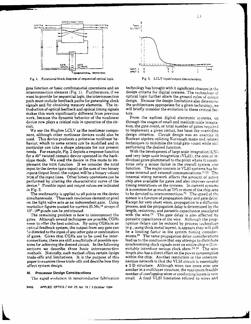
INTEICCNNEC 7 CNS
NP~Jrs outJTs NPUT 0 0 I r
Fig. 1. Functional block diagram of sequential optical logic. Fig 2. LCLV input/output characteristic_
gate function or basic combinatorial operations and an technology has brought with it significant changes in thtinterconnection element (Fig. 1). Furthermore, if we design criteria for digital systems. The technology ofwant to provide for sequential logic, the interconnection optical logic further alters the ground rules of circuitpath must include feedback paths for generating clock design. Because the design limitations also determinesignals and for obtaining memory elements. The in- the architectures appropriate for a given technology, wetroduction of optical feedback and optical timing signals will briefly consider the evolution in these critical fac-makes this work significantly different from previous tors.work, because the dynamic behavior of the nonlinear From the earliest digital electronic systems, updevice now plays a critical role in operation of the cir- through the stages of small and medium scale integra-cuit. tion, the gate count, or total number of gates required
We use the Hughes LCLV as the nonlinear compo- to implement a given circuit, has been the overridingnent, although other nonlinear devices could also be design criterion. Circuit design was an exercise inused. This device produces a pointwise nonlinear be- Boolean algebra utilizing Karnaugh maps and relatedhavior, which to some extent can be modified and in techniques to minimize the total gate count while stillparticular can take a shape adequate for our present performing the desired function.needs. For example, Fig. 2 depicts a response function With the development of large scale integration (LSI)for a 450 twisted nematic device operated in the back- and very large scale integration (VLSI), the cost of in-slope mode. We used the device in this mode to im- dividual gates plummeted to the point where it consti-plement the NOR function. If we consider the total tutes only a minor factor in the overall system costinput to the device (gate input) as the sum of two binary function. The major concern in VLSI systems has be-.nputs (input lines), the output will be a binary valued come internal and external communications. '21,: 2 TheNOR of the input lines. Other binary operations can be internal wiring network affects the amount of activeperformed by altering the characteristic curve of the chip area available for gates and also imposes severaldevice." Possible input and output values are indicated timing restrictions on the systems. In current systemsin Fig. 2. it is common for as much as 70% or more of the chip area
The nonlinearity is applied to all points on the device to be devoted to interconnections. 23 The speed of thesimultaneously. Thus each resolution element or pixel system is a function of propagation delay and gate delayon the light valve acts as an independent gate. Using Except for very short wires, propagation is a diffusionresolutio.n figures quoted for current SLN~s, 16 arrays of process, and the propagation delay is determined by theI0W-I06 pixels can be anticipated. length, resistivity, arid parasitic capacitance associated
The remaining problem is how to interconnect the with the wire.2'I The gate delay is also affected bygates. Although several techniques are possible, CGHs parasitic capacitance of the wire. Although the prop-seem to offer the best solution. By using CGHs in an agation delays can be reduced by process technologyoptical feedback system, the output from any gate can (e.g., using thick metal layers), it appears they will stillIedirectedtotheinputofanyothergateorcombination be a limiting factor in the system timing consider-of gates. Given that CGHs are to be used for inter- ations.25 The same propagation delay considerationsconnections, there are still a multitude of possible sys- lead us to the conclusion that any attempt to distributetems for achieving the desired circuit. In the following synchronizing clock signals over an entire chip will in-sections we describe three basic interconnection evitably introduce serious clock skew.24 .2 6 The wiremethods. Naturally, each method offers certain design length also has a direct effect on the power consumptiontrade-offs and limitations. It is the purpose of this within the chip. Another restriction in the intercon-paper to examine those trade-offs and describe how they nection network is that the VLSI circuit is essentiallyaffect system design. a 2-D structure. Although wires can cross over one
another in a multilayer structure, the maximumn feasibleIII. Processor Design Considerations number of overlapping wires or conducting layers is very
The rapid evolution in semiconductor fabrication small. A final VLSI limitation related to wires and
3466 APPLIED OPTICS / Vol. 23, No. 19 / 1 Oclober 1984

20
,,)imomcati'n is the problemn )l1'in-011tS. 'File num- conjunction with the reduction in device arta utiJJati,,n.hier of pins available for communicatitn hetween the This restriction makes many interesting ;rchitep t1;r(-
i ip and the rest of the system i :; -evorelv limited. In such as cellular 1pramids very difficult ' mopl,,VLS.I vstems there is a great deal ot interest in systolic in VIS[.0 The optical system, on the t iher hand. h!s
arrays and related architectures that achieve high no such restriction. Thus pyramid ..tructures and ,,i;crproce.-ing throughput rates for certain algorithms by architectures requiring complex interconinections w,, ldexploiting concurrency and pipelining. -i. However, merit consideration for an optical logic system.highly parallel systems usually require a large number Finally, the problem of pin-outs is also alleviated hVOf input or output data channels, and highly pipelined the optical logic system described here. The ,tsystems frequently require a large number of input system naturally can accept a large number of paralilcontrol lines. Thus the extent of concurrency and pi- inputs and at the same time generate a large number oA
pelining which can be achieved is directly limited by the parallel outputs. Thus the problem of communicationnumtber of pin connections to the ctIip.,7 Pin-out between separate devices is eliminated as is the limi-constraints will similarly limit the efficiency of other tation on concurrent/pipelined processing mentionedVLSI processors. above.
One effect of these communication limitations is the Having shown that the communication restrictionsemphasis on highly structured and regular intercon- which dictate design criteria for VLSI do not apply tonection patterns. Modular building blocks such as the optical logic system, what are the major limitin,,programmable logic arrays IPLAs), read-only memories factors for the optical system'? Given that we are tg-
1 ROMsl, and standard cells are heavily relied upon to noring the important question of gate switching timesproduce VLSI chips. Another effect is the close scru- at this point, with the expectation that future devel-tiny of data flow by VLSI designers to find ways in opments will improve this parameter, the most impor-which pipelining can be maximized and to find ways of tant factor seems to be the space-bandwidth producteliminating synchronization requirements) 5s All this (SBWP) of the holograms which form the intercon-has led to a concentration of interest in special purpose nections. This is, we should point out, loosely con-processors such as wave front array processors and nected to the question of wire lengths, although it issystolic arrays.' 6 ,28.29 more appropriately associated with a measure of the
For the optical logic system described here, the major interconnection complexity and regularity. In thedesign considerations are admittedly not so well defined following sections we describe three different inter-as for VLSI at this point. However, it is clear that the connection schemes which differ in their interconnec-cost function is much different than for the integrated tion complexity: a space-invariant system with a per-circuit systems. In particular, most of the communi- fectly regular structure with minimal space-bandwidthcation costs affecting VLSI design are not associated requirements; a space-variant structure with severewith the optical system. For the systems described space-bandwidth requirements; and a hybrid system.here, all interconnections have the same length to first The constraints associated with these systems will de-order due to their optical imaging or Fourier transform termine the architectures which are most appropriatenature. Thus synchronization problems due to clock for implementation with the optical logic system.skew should be eliminated, making large syncrhonized Since there are significant differences between thesystems more feasible. Being able to synchronize the factors which limit VLSI and our optical logic system,circuits eliminates the need for handshaking or other one might ask if there are application areas specificallyasynchronous techniques which introduce various well suited to one or the other. Due to the restrictionsamounts of waiting time for individual circuit elements. on communications, VLSI systems are being particu-Although an interconnection path length would still larly considered for applications which involve veryultimately affect the speed of the optical system, since regular structures and simple data flow that can bethe path length is constant, it is not a design variable handled with only local communications. This has ledthat affects architectural decisions. The other prob- to the development of systolic array architectures .2- . 9
lems associated with wire length, namely, power con- These structures are well suited to many vector-matrixsumption and device area utilization, are not relevant and matrix-matrix operations.to the optical logic system. With the optical systems, However, there are many common algorithms whichnone of the active device area is occupied by intercon- inherently require global communications. Thesenections. Also the power consumption of the system cannot be conveniently handled by VLSI but could, inis independent of the interconnection path length. principle, be implemented with the optical logic sys-
A striking feature of the optical system is the inter- tem.31 For example, although the discrete Fourierconnection flexibility. As we pointed out, wire length transform (DFT) can be expressed as a problem in-is not a problem for an optical system. Thus, for ex- volving only local communications, the fast Fourierample, a gate may be connected to the most distant transform (FFT) algorithms inherently require globalgates on the device as easily as it is connected to its communications due to their pyramidlike butterflynearest neighbors. With VLSI, even if such intercon- structure. Thus by going to an optical logic system, onenections were not impractical due to wire length re- might be able to take advantage of the FFT structurestrictions, they would be impractical due to the inevi- and speed at the hardware level. Other examples oftable problems of wires crossing over one another in communication-limited operations are value counting
I October 1964 / Vol. 23, No. 19 / APPLIED OPTICS 3467

21
,A-- .T.----- an N X N array of subholugrans on the CGH and :n.X . array ofgates on tie nonlinear device. Each .ub-hologram must be capal)le of addres.ing any of the N'2
gate inputs. The num)er of addressable points is equalto the number of complex-valued samnples in a subho-
4logram assuming a Fourier hologram. Thus the itualSBWP of each subhologram is
GATE lrS pTq
2N T (
ARRA MOLOC, AMGATEr where p 2 is the number of resolution elements in theAPRAY hologram used to represent one complex-valued sample,
and q2 is a factor representing the amount (if over-Fig. 3. Space-variant interconnection system. In general the ho- ad li i t o gr p nge mn t pi ove-logram produces multiple diffraction orders, only one of which is sampling in the hologram plane. Generally p-> I be-
used. cause the complex sample values must be encoded intothe hologram, e.g., as real values. Also we generallyhave q2 > 1 to avoid cross talk. These problems are
or histogramming and regional property computation, discussed below.both of which require global summing operations.3 ° The entire interconnection hologram consists of \'-Additional thoughts on parallel optical digital com- subholograms, one for each gate. Thus the total SBWPputers and applications to symbolic substitution are of the hologram is ST wheregiven in Ref. 11.IV. Space-variant Interconnection Method Sr N 2Ss =p
2q2 .V', (2)The most general interccnnection system is one in Because ST , N 4 , we expect that the hologram SBWP
which gate output be connected to the input of ST will quickly become the limiting factor as .\ in-any gcan creases. We will verify that below, but first we need to
any gate or combination of gates. If we think of the study the cross talk in the gate-input plane to get ainterconnection systein as imaging the gate output array feeling for the expected values of q 2
plane onto the gate input array plane, this approach The cross talk can he represented by a, the ratio be-represents a space-variant imaging system. The image tween gate inputs of the worst-case (largest) zero valueof a gate output consists of a collection of spots (the and the worst-case (smallest) one value / :
impulse response of the system for that particular point)
that illuminate the appropriate gate inputs and form a = to// (13)the circuit interconnections. Because each object point We require a < I to distinguish all possible zero and one(gate output) sees a different impulse response (inter- states. Assume that the intensity profile of a single gateconnection pattern) this represents a general space- input reconstructed from a subologran is F(x,)t
variant system. A space-variant system has been built [The reconstructo o a subologram a berereto demnon'strate the concept of sequential optical logic. [The reconstruction of a subhioiograrn can be repre-The demonstration circuit that was implemented sented by a set of Dirac delta functions (one for each
addressed gate input) convolved with the Fouriercomprises a ring oscillator which generates a clock signaland a master-slave flip-flop driven by the clock. This holoranm. Then F(x,y) VV aX 2unc Thus thesystem is operational arid described in another torm hnFxy [~~~''lTu h
worst-case one value is the integral of F over the definedpaper.1
A schematic diagram of the optical system used for area a of the gate input:the space-variant interconnections is shown in Fig. 3. t= (x)dxd'. k4)First, the gate outputs are imaged onto the intercon- "nection hologram. This CGH consists of an array of The worst-case zero level occurs when all gates havesubholograms, one subhologram for each gate. When their maximum input levels except for the gate inilluminated by its corresponding gate output, a subho- question which has a zero input level. If each gate haslogram will reconstruct an image on the write side, or m input lines (a fan-in of m) and gates are coal iguous,
gate input side, of the light valve. The reconstructed the worst-case zero can he shown to beimages are simp'.e dot patterns, each bright dot illumi-nating a gate input. Because the reconstructed images 10 = m F(xy- dxdy - )d'r' d -
can be designed to illuminate any combination of gate IJfA ffainputs, arbitrary interconnections are possible. As where A is the area of the entire gate array. This as-shown in Fig. 3, the desired interconnections are formed sumes that the spatially integrated sum of gate inputin one particular diffraction order. Typically, a con- lines from different subholograms is effectively an in-jugate image will also be produced, in which case it can coherent sum. Note that such inputs actually add co-be used to probe the system without affecting system herently but that they produce interference fringes.operation or to access the system outputs. Spatial integration over these fringes results in the ef-
While this interconnection scheme allows complete fective incoherent summation. Similarly, the abovegenerality, a price is paid in terms of the space-band- equation assumes that the gate inputs reconstructedwidth product requirements on the CGl. Let there be from a single subhologram also can be modeled as
3468 APPLIED OPTICS / Vol. 23, No. 19 / 1 October 1984

22
FT
INPUTARRAY
Fig.-I. pace-invariant interc,)nnectlun system. Fig. 5. Example of a pace-ilwarlant interconnecti n net.%ork.
Nodes represent gates, and arrows are the (opticalI
adding incoherently. This will be essentially true if a interconne( lions.
pseudorandom phase is applied to the n distinct gateinputs, where n is the fan-out. Combining the above The hologram coding parameter p, defined in Eq. (1),equations we get for the case of a Burckhardt hologram, :I2 has a minimum
value of 3 assuming square cells. Having found that qw rfe u- will typically be in the range of 2-3, we conclude that the
where E1 is the fraction of the single-gate input inten- maximum feasible number of gates corresponds to asity profile which falls within the defined area of that value of pq of the order of 10. From Eq. (2) and thegate: above SBWP, we find that the gate array dimension is
N X N whereE0 = Jf , -dxd JJ F(xv)dxdy. (7)
We define the minimum gate area as ao = 1/Ls2H, where for space-variant interconnections. Becaus2 this is lessLsq is the width of each (square) subhologram. Al- than the SBWP capabilities of some spatial light mod-lowing for N2 contiguous gates implies a Nyquist fre- ulators, the CGH is the limiting element.quency /-v, = NILsH. The actual gate area is Since the space-variant system allows arbitrary in-
terconnections, the only other possible limitation on theS= q( circuits that can be implemented is the requirement
where q is the oversampling factor defined by fsamp = that all gates must perform the same binary operation,qf[Nv and fmp is the ;ampling rate. Obviously, as q e.g., NOR in this case. However, since all the Booleanincreases E0 approaches unity and ci approaches operations may be constructed out of NOR gates, thiszero. does not limit the types of processing operations that
We now consider an example. If we use a triangle can be perfurmed. Another feature is that circuits wxithfunction in x and y for the aperture (window) function any degree of inherent pa illelism, or lack thereof, canof each subhologram, its Fourier transform is a 2-D sinc2 be implemented with approximately equal ease.function, V. Space-invariant Interconnection Method
F(x.y) = sinc 4(x/2) sinc 4Lv/2). (9) If one is willing to compromise on the arbitrariness
Choosing q = 2 yields a cross talk ax = (0.11)m, so that of the gate interconnections, a substantial increase in3-input gates cause a cross talk of 0.33. Thus for NOR the possible number of gates results. The extreme casegates the thresholding of the nonlinear device could be is a totally space-invariant interconnection. This is theperformed anywhere between relative gate input levels idea behind the interconnections of the processor sug-of 0.33 and 1.0. In this case the sampling rate is twice gested by Huang. 12 We implement this interconnectionthe Nyquist rate. Increasing q permits a larger fan-in, method optically via an imaging system with a space-e.g., q = 3 implies ct = (0.0082)m, and a cross talk of 0.33 invariant filter using one simple hologram for the entirepermits 40-input gates to be used. Also note that use circuit (Fig. 4). The filter has an impulse responseof a more appropriate aperture function could permit consisting of a series of spots which illuminate the ap-smaller values of q. propriate gate inputs as in the space-variant case.
To estimate the SBWP that can be written onto a However, in this case, the impulse response (intercon-CGH, we assume the CGH is written using electron- nection pattern) is the same for every gate output, andbeam lithography, as was the case for the experimental the gate inputs are addressed relative to the position ofdemonstration of the optical logic system. 14 This the gate output. The space-variant method worked onelectron-beam system has written linewidths down to the basis of absolute addressing.0.5 pm and has a maximum file size of 1.024 mm on a An example of a space-invariant interconnectionside. Files can be stitched together to yield a maximum pattern is shown in Fig. 5. Each dot in the figure rep-size of 10cm on a side. If we minimize the effect of the resents a (NOR) gate, and each arrow represents an in-stitch error by making the file boundaries coincident terconnection from the output of one gate (dot) to thewith subhologram boundaries, an effective SBWP of input of another. Each gate is considered to have one4 X 101" is attainable, additional unconnected input line for an enable/disable
1 October 1984 / Vol. 23, No. 19 / APPLIED OPTICS 3469

22
signal. A particular circuit is implemented by disablingthe appropriate gates. In the NOR case, a gate is dis- ...... .abled by projecting light onto it (i.e., putting a I onto thle. . .
unconnected input line). With the illustrated inter-connection pattern it is possible to transfer data in .. . .
various directions without getting unintended feedbackloops. The major limitation of this interconnectionmethod is that the implementation of many circuits willrequire a large number of gates to be disabled. Ob- .... ...viously, some circuits can utilize the gates more effi- -4... .ciently than others.
As an example, a good utilization of gates can be . .
achieved for some digital systems that perform parallelimage processing operations over an array of imagepoints. In this discussion, we define image point as a so,
resolution element of an image to be processed, whilewe use the term pixel to refer to a resolution element on ACTIVE DEVICE AREAthe nonlinear device that forms one gate. Parallel Fig. 6. Example of a system with space-invariant interconnectionsimage processing systems generally require several gates for parallel image processing operations. The system has three gatesper image point. We refer to the set of gates associated per image point: x,y, andz. These three gates are called a logic ele-with an image point as a logic element. Here we con- ment. The gates are represented by dots in the figure, and theirsider the important case of identical logic elements. Let physical layout on the active device area is shown. The x subarraythe number of gates per logic element be denoted by is composed of all the x gates in the processor with similar subarraysr. for the y and z gates. This configuration allows arbitrary intercon-When r is equal to three, each logic element has three nections within logic elements axd also achieves a high gate
gates, and we label these gates x, y, and z. A possible utilization.physical layout for all the individual gates in the pro-cessor is shown in Fig. 6, where each gate is denoted by must be an unused area, or buffer zone, separating thea black dot. The active device area contains three z, y, and z subarrays. This buffer zone is small whenidentical subarrays of gates. The x subarray is a col- connections between logic elements in certain directionslection of every gate in the processor labeled x, one from are limited in length (one gate distance for nearesteach logic element. Similarly, the y and z subarrays are neighbor connections) but can become quite large whencomposed of all they and z gates, respectively. Thus distant logic elements are connected in certain direc-the number of gates in each subarray is equal to the total tions. Distant logic elements can be connected in othernumber of logic elements (which is equal to the total directions, however, without requiring large buffernumber of image points to be processed in parallel). zones. With four or more gates per logic element (r >_The number of subarrays is equal to r. All gates are 4) some restrictions apply on the interconnections bothidentical and communicate with each other in a space- within and between logic elements. A set of intercon-invariant manner. With up to three gates per image nection rules can be enumerated for a given r >_ 4. Wepoint, interconnections within a logic element can be also note that the subarrays in Fig. 6 need not be squarechosen arbitrarily, and interconnections to and from a but can be other shapes to better fill the active devielogic element can be chosen almost arbitrarily. Once area.these interconnections are chosen, all logic elements are These ideas are further illustrated with a simple ex-connected identically. ample that uses three gates per image point as shown
Figure 6 shows a (space-invariant) point spread in Fig. 7. Each image point is labeled E, and each isfunction that connects the output of an x gate to the connected to its four nearest neighbors: A, B, C, andinput cif the corresponding z gate (within-logic element D. This circuit implements a binary version of a I.a-connection) and also to the input of the y gate of the placian edge detector-if the value of image point E islogic element located two positions down in the array 1, and at least one of its nearest neighbors is 0, 1 is out-(between-logic element connection). Ppcause of the put at image point E. Otherwise, zero is output. Thelocations of the gates on the device, this point spread point spread function (PSF) that implements this cir-function connects the outputs of the y and z gates to cuit is depicted in Fig. 8. As this PSF is convolved withpoints that are either off the device or in an unused area the gate array, all interconnections are accounted for.of the device; thus these connections have no effect. Since the holographic element used in this inter-
One restriction on the between-logic element inter- connection system is simple, a very large number ofconnections is that the output of one gate cannot be gates can be interconnected. Even allowing the PSFconnected to the same gate of a different logic element, to address simultaneously any set of gates in the array,e.g., x gate to x gate, without also connecting the y gate the space-bandwidth product required of the hologramtoy gateand z gatetoz gate. Theonlyotherrequire. isoftheorderofp2 q2 N2 [see Eq. (l). Thus ifthefullment is on the directions of long between-logic element SBWP availahle with the CG- could he exphoited ininterconnections. Because of boundary effects, there this system and if p~q2 - 100, _,I X l)" gates iould he
3470 APPLIED OPTICS / Vol. 23. No. 19 / 1 October 1984

24
INPUT a TO - r --E NEAREST F. T.-
-A '-- ,--J NEIGHBORS WAGING ---------- 4
Z OUTPUT
GATE F YIGST
OUT PUT hOLOGIRAMf
*A ARRAY SECONO GATE
.O.E .8 hOLOGRAM INUTARRAY
SC Fig. 9. Hybrid interconnection system. The first hologram is aspace-variant element as in Fig. 3. The second hologram is an array
UPLIAM 8"t KECIOR of space-invariant filters.
Fig. 7. Example of a circuit with three gates per image point whichcould be implemented with the space-invariant arrangement of Fig. gates, whereas in the space-variant case the number of6. This circuit implements a binary Laplacian edge detector on an distinct interconnection patterns is in general large andimage. All image points are processed in parallel. Each image point potentially equal to the number of gates. These twois denoted by E, and each is connected to its four nearest neighbors: approaches represent the extreme cases in terms of the
A, B, C, and D. space-bandwidth requirements they place on the CGH.The trade-offs between these two is increased flexibilityat the cost of increased hologram complexity. Since thespace-invariant case generally suffers from inefficientgate utilization and the space-variant system is limitedby the hologram to the number of gates it can address,
Ci it is worthwhile considering if there is a combination oftechniques which can achieve high gate utilization ef-ficiency and at the same time be limited in gate countonly by the space-bandwidth product limitations of the
. . . ... .spatial light modulator.Our approach to this has been to consider a hybrid
system which combines space-variant and space-in-variant interconnections. The idea is to define a finitenumber M of distinct interconnection patterns. Wethen assemble our circuit using only these M intercon-nection patterns. If the total number of gates is N 2, weassume
ACTIVE DEVICE AREAI << M << N2 (10)
Fig. 8. Space-invariant interconnection pattern required for the so that this system is truly intermediate between thebinary Laplacian edge detector of Fig. 7. space-variant and space-invariant cases. If M is large.
we anticipate that we have almost complete flexibilityinterconnected. The hologram for this system could in designing our circuit.also be recorded optically. In either case, the number The optical implementation of this system is sche-of gates with the space-invariant interconnection matically diagrammed in Fig. 9. Here the gate outputmethod is limited by the SBWP of the spatial light array is imaged onto a space-variant filter element asmodulator. in Fig. 3. The purpose of this element is to deflect the
As mentioned above, the method of disabling gates light from each gate output through one of M subholo-to implement circuits decreases the number of gates grams in the second CGH (Fig. 9). These subhologramsthat are actually used and, therefore, severely restricts act as space-invariant filter elements which produce thethe variety of operations that can be performed effi- M different interconnection patterns in the gate inputciently. It also adds a degree of complexity to the sys- plane.tern. However, this method of optically disabling gates Although the space-variant element would appear toalso provides a potential advantage-it provides a have the same space-bandwidth limitations as in themeans of easily rewiring the system in real time by simple space-variant case, we note that the SBWP ofchanging the disable signals. This could offer consid- each subhologram in this plane is now of the order of Merable flexibility in making an adaptive system. rather than of the order of N 2. Thus the total SBWP
requirement in this element is much less than in theVI. Hybrid Interconnection Method previous space-variant case. The subholograms in the
At this point we have seen two approaches to inter- space-invariant element generally have a relatively lowconnecting gates. In the space-invariant case there is SBWP.only one interconnection pattern which is applied to all The SBWP Ss, of a subhologram in the first holo-
1 October 1984 / Vol. 23, No. 19 / APPLIED OPTICS 3471

25
grain HI is hologram to the illuminated f, subhologram. AU kad-ditions here are incoherent because we are effectively
Ss, = P NiM. (01) averaging over fringe patterns again. The worst case
where Al is the number of subholograms in the second one-level gate input is simply the integral ofg(x,y overhologram H,-, and p2 and q1 represent coding and ov- the illuminated subhologram q, thus the intrahohgranersampling factors, respectively, as in the space-variant cross talk aH isinterconnection section. Similarly, the SBWP of asuhhologram of H2 is in the worst case J 'O M ffjgx,)dxdy
Ss, = piq2.N2, (12) an -y (16)
where N 2 = number of gates. This worst case allows the ff.R4Z.y)dxdy
H2 subhologram to address any n gates in the array. If The total cross talk a i. the sum of contributions to thethe gates it addresses are localized, i.e., are all contained worst-case zero-level gate input from both sources ofin the same portion of the array, its SBWP can be sig- cross talk divided by the worst-case one-level gate input.nificantly reduced by introduction of a carrier fre- To first order in ap and an it is given byquency.33 Since Ht consists of N2 subholograms andH2 consists of M subholograms, their total SBWPs are a a f, (17)given by where ap is the interpixel cross talk.
Now we look at an example. Again taking a 2-DSri = piqMN 2 Sr, = p2qjMN 2, (13) triangle function as the subhologram aperture function
and here again ST, is a worst-case estimate. If we as- in the HI plane, g(xy) in the H2 plane is given by F(x,y)
sume both holograms are written in the same manner, of Eq. (9). Now the intensity profile F(x,y) in the gate
STI = ST2 m Sr and P, P2 = p, from which it follows input plane is the squared modulus of the convolution
that q = q2= q; thus of this triangle aperture function with the sinc functionresulting from the rect aperture function in the H2
ST p2q2MN 2 .(14) plane. Taking, for example, q = 3 and calculating ap
As in the space-variant case, we need to analyze the from Eq. (6) and -tH from Eq. (16), Eq. (17) yields
cross talk to estimate q. a = m(O.0025) + nM(0.0018), (1b6
For the hybrid interconnection scheme, two sourcesof cross talk exist. Interpixel cross talk occurs between where m is the fan-in to each gate. For example, if
pixels in the gate-input plane and is analogous to the eight-input gates are used and we allow a = 0.50, we can
cross talk treated in the space-variant interconnections have fifty-three different interconnection patterns each
section. Intrahologram cross talk occurs between with a fan-out of five. These numbers are strongly
subholograms in the second hologram and also con- dependent on the aperture function. Since no attempt
tributes to noise in the gate-input plane. (We assume to optimize, or even improve on, the aperture function
negligible cross talk at the first hologram because it is was made, one can expect a significant improvement in
in the image plane of the gate-output array.) these numbers by using a more appropriate aperture
The interpixel cross talk is completely analogous to function.
the cross talk in the space-variant interconnection case Thus, as in the space-variant case, we conclude thatwhen applied to H 2 and the gate-input array, and the the maximum number of gates corresponds to a value
same equations apply. ofpq of the order of 10. Again using ST = 4 X 1Ot (see
To analyze the intrahologram cross talk, we have to Sec. IV), from Eq. (14) we get MN 2 - 4 X 10, and thus
find the effect of this cross talk in the gate-input plane. for M - 50 different interconnection patterns, we get
We assume that each HI subhologram addresses only of the order of 107 gates or an N x N array with N
one H2 subhologram and that all H 2 subholograms have 2000-3000, which is above the SBWP capabilities of
the same fan-out n. Through a given H 2 subhologram presently available spatial light modulators.
k. there are only n subholograms of HI that can address To implement an arbitrary circuit with the hybrid
a given gate input p. Any unintentional illumination interconnection method, the M interconnection pal-
of k from one of these HI subholograms will contribute terns may be considered a basis set from which one
cross talk to gate p. The worst-case (maximum) zero constructs the desired interconnections. With a largeinput to p then occurs when all n of these HI subholo- enough M, any circuit can be implemented. However,
grams illuminate the nearest-neighbor subholograms the potential of this architecture can be exploited more
of k. We then sum this result over all Ha subholograms fully by implementing circuits with a high degree of
h to obtain the worst-case zero-level input, regularity or symmetry. Examples include parallelarrays, such as systolic arrays and cellular automata.
ign = E n gx,)dxdy(15) As mentioned earlier, the principal motivation behindIt. ., x"dd'the systolic array concept is the adaption to the limi-
where g(xy) is the intensity profile divided by n in the tations of VLSI structures.H,2 plane due to the illumination (if one H2 subhologram A more appropriate application of our hybrid inter-
by one 11, subhologram and is analogous to F(xy) in our connection scheme is that of 2-1), or more generallyprevious derivation. aN.V is a nearest-neighbor sub- N-dimensional, processor arrays. A conceptual di-
3472 APPLIED OPTICS / Vol 23, No. 19 / 1 October 1984

26
p : late to the device used as a gate array. In particular, thespeed of current devices is a major bottleneck. Currentwork in optical bistability may alleviate that restriction,
S although significant progress will have to he made he-fore that technology develops into functional devices.
We thank B. H. Soffer and S.-Y. Kung for manyuseful discussions in connection With thit: research.This work was supported by the Air Force Office ofScientific Research under grant AFOSR-81-0182.
Portions of this paper were presented at the TenthInternational Optical Computing Conference. 34
Fig. 10. Two-dimensional processor array as an example of the useof the hybrid interconnection system of Fig. 9. Connections withineach block are space-variant, and connections between blocks are
space-invariant. References
1. A. Armand, A. A. Sawchuk, T. C. Strand. D. Boswell, and B. H.Soffer, 'Real-time Parah-Ir Analog-to-Ditital Conversion.' Opt.
agram of a 2-D array is shown in Fig. 10. Each block Lett. 5, 129 (1980).
represents a processing element made up of a number 2. P. Chavel, A. A. Sawchuk, T. C. Strand, A. R. 'anguay, Jr., andof gates connected in some arbitrary manner. Each B. H. Soffer, "Optical Logic with Variahle-Grating-Mode Liq-block may be identical to the others or different, al- uid-Crvstal Devices," Opt. Len. 5.398 (1980).though the more similarities there are between blocks 3. A. A. Sawchuk. T. C. Strand, and A. R. Tanguay, .Jr., "Nonlinear
the fewer interconnection patterns are needed. The Real-time Optical Signal Proces.ing," USCIPI Report 1080, USC
connections between blocks will typically be space- Image Processing Institute (1982).
invariant. Although the figure depicts only nearest- 4. S. H. Lee, Ed., Optical In/ormation Proces.ing iSpringer, New
neighbor connections between blocks, much more York. 1981), Chap. 7.complicated interconnection patterns, without regard 5. S. A. Collins, Jr- M. T. Fatehi, and K. C. Wasmundt. "Opticai
Logic Gates Using a Hughes Liquid Crystal Light Valve," Proc.to the physical distance between connected blocks, may Soc. Photo-Opt. Instruin. Eng. 232, 168 (1980).be made almost as easily, permitting implementation 6. B. Horwitz and F. Corbett, "The PROM-Theory and Applications
of N-dimensional arrays. Thus we have a processor for the Pockels Readout Optical Modulator." Opt. En6. 17, 353array with global as well as local interconnections. (1978).
This concept may also be applied to computational. 7. C. Warde, A. M. Weiss, A. D. Fisher. and J. 1. Thackara. "Optical
algorithms that require global interconnections, which Information Processing Characteristics of the Nlicrochannel
are often difficult or inefficient to implement using Spatial Light Modulator," Appl, Opt. 20, 2066 (1981,.
VLSI. In this case, the blocks in the figure are often 8. J. Tanida and Y. Ichioka. "Optical Logic Array Processing,"
identical, but the interconnections between the blocks Proceedings, Tenth lnterrnational Optical Computing Confer-
are space-variant. Frequently, however, as in the case ence, IEEE Catalog. 8.3CHISWo-4 (1983), p. 18.ofate FF T . entionedearlr, thoereril a highe dee 9. R. A. Athale, H. S. Barr, S. H. Lee, and B. J. Bartholomew.of the FFT mentioned earlier, there is still a high degree "Digital Optical Processing," Proc. Soc. Photo-Opt. Instrum. Eig.of symmetry among the connections between blocks. 241,149(1980).TIhus this class of algorithms is also particularly well tO. D. H. Schaefer and J. P. Strong Ill, "TSE Computers," Proc.
suited to the hybrid interconnection scheme. IEEE 65, 129 (1977).11. A. Huang, "Parallel Algorithms for Optical-Digital Computers,"
VI1. Conclusion in Proceedings, Tenth Internatiur.al Optical Computing Con-
We have described some of the architecture and de- ference, IEEE Catalog 83CH1880-4 (1983), p. 13.
sign considerations which affect the implementation of 12. A. Huang. "Design for an Optical Geneial Purpose Digil
sequential logic in an optical system. Computer," Proc. Soc. Photo-Opt. Instrum. Eng. 232. 119
Whereas in VLSI systems, communication costs are 1(1980).heajr liming LSd es acor n tican sst 13. H. Barr and S. H. Lee, "A Digital Optical Processing System,"the major limiting design factor, in the optical system, in Proceedings. Tenth International Optical Computing Con-
the communication costs are much less severe. Thus ferece, IEEE Catalog. 83CH1880-4 1198.3), p. 171.many architectures which may be impractical in VLSI 14. B. K. Jenkins, A. A. Sawchuk, T. C. Strand, and B. H. Soffer.due to communication problems may be implemented "Sequential Optical Logic Implementation." J. Opt. Soc. Am. 72,easily in an optical system. 1721A (1982); B. K. Jenkins, A. A. Sawchuk, T. C. Strand. R.
The interconnection network can be produced in Forchheimer, and B. H. Soffer, "Sequential Optical Logic Ir-
several different ways. We discussed three methods: plementation," Appl. Opt. 23. 3455 (1984).
a space-variant technique whicl, allows arbitrary in- 15. .J. Grinberg. A. Jacobson, W. Bleha. L Miller, L Fraas, D. Boswell.
terconnections but is limited by the SBWP of the CGH; and D. Myer, "A New Real-Time Non.Coherent to Coherent
which requires only simple Light Image Converter. The Hybrid Field Effect Liquid Crystalspace-invariant system wLight Valve," Opt. Eng. 14, 217 (1975).
CGHs but suffers from low gate-utilization rates; and 16. U. Efron. B. H. Soffer, M. J. Little, J. Grinberg, and M. A. Mo-
a hybrid of these two techniques which provides large nahan, "Applications of Silicon Liquid Cry-ital Light Modulatorsgate counts with high gate-utilization rates. for Optical Data Processing," Proc. Soc. Photo-Opt. Instrum. Fng.
The major limitations of the system at this point re- 388. 152 (1983).
1 October 1984 / Vol. 23. No. 19 / APPLIED OPTICS 3473

17. H. M. Gibbs, S. L. McCall, and T. N. C. Venkatesan, "Optical 27Bistable Devices: The Basic Components of All-Optical Sys-tems," Opt. Eng. 19, t63 (1980).
18. E. Abraham. (. T. Seaton, and S. D. Smith, "The Optical Com-puter," Sci. Am. 248, 35 (Feb. 1983).
19. P. W. Smith and W. J. Tumlinson, "Bistable Optical DevicesPromise Subpicoaecond Switching." IEEE Spectrum 18,26 (June
1981).20. C. R. Bowden, M. Ciftan, and H. R. Rohl, Eds., Optical Bistability
(Plenum, New York, 1981).21. C. A. Mead and L. A. Conway, Eds., Introduction to VLSI Sys-
ters (Addison-Wesley, Reading, Mass., 1980), Chap. 8.22. L. S. Haynes, R. L Lau, D. P. Siewiorek, and D. W. Mizell, "A
Survey of Highly Parallel Computing," Computer 15, 9 (Jan.1982).
23. J. W. Tompkins and S. Hollock, "The Impact of Multi-LevelMetalization on Semi-Custom LSI," in Proceedings, CustomIntegrated Circuits Conference (1982), p. 276.
24. Ref. 21, C. L Seitz, "System Timing," Chap. 7.
25. C. L. Seitz, "Ensemble Architectures for VLSI-A Survey andTaxonomy," in Proceedings, 1982 Conference on Advances inResearch in VLSI MIT, Cambridge, 1982, p. 130.
26. H_ T. Kung, "Why Systolic Architectures?" Computer 15,37 (Jan.1982).
27. D. M. DeRuyck, L Snyder, and J. D. Unruh, "Processor Dis-placement: An Area-Tree Tradeoff Method for VLSI Design,"in Proceedings, Conference on Advances in Research in VLSI,MIT, Cambridge, Mass. (1982), p. 182.
28. S.-Y. Kung, K. S. Arun, R. J. Gal.Ezer, and D. V. Bhaskar Rao,"Wavefront Array Processor. Language, Architecture, and Ap-plications," IEEE Trans. Comput C-31, 1054 (1982).
29. Ref. 21, H. T. Kung and C. E. Leiserson, "Algorithms for VLSIProcessor Arrays," pp. 271-292.
30. A. Rosenfeld, "Parallel Image Processing Using Cellular Arrays,"Computer 16, 14 (Jan. 1983).
31. S.-Y. Kung, Electrical Engineering Department, University ofSouthern California; private communication.
32. C. B. Burckhardt, "A Simplication of Lee's Method of GeneratingHolograms by Computer," Appl. Opt. 9, 1949 (1970).
33. S. Lowenthal and P. Chavel, "Reduction of the Number ofSamples in Computer Holograms for Image Processing," Appl.Opt. 13, 718 (1974).
34. P. Chavel et al., "Architectures for a Sequential Optical LogicProcessor," in Proceedings, Tenth International Optical Com-puting Conference, IEEE Catlog 83CH 1880-4 (1983), p. 6.
3474 APPLIED OPTICS / \ol 23, No. 19 / 1 October 1984

28
Cimputer-generated holograms ftr space-variant interconnections in optical Iogic soyotems
B.K. Jenkins and T.C. Strand*
Image Processing Institute, University of Southern California,Los Angeles, California 90089-0272
Abstract
Interest in optical logic systems has been revived recently for several reasons. Onemajor reason is that optics provides a means for overcoming the communication bottleneckswhich are beginning to limit the development of electronic systems both at the chip level
and at higher levels. This stems from the fact that an optical system in effect processes alarge number of independent parallel channels. However, in attempting to implement opticalinterconnection networks, one is quickli faced with the need to realize space-varlanl:nterconnections. In this paper we describe various means of achieving space-variantinterconnections for optical logic systems. All of the techniques use computer-generaLedholograms (CGH) as combination beam-splitting and beam directing elements. Thespace-variance can be obtained with either a direct approach where a separate CGI elementforms the interconnections for each logic element, or with a basis set approach whichprovides significant reductions in the CGH storage requirements. Examples of the differentapproaches are discussed.
Introduction
There is a recurring interest in the subject of space-variant optical processinq.There are two major questions to be asked on this subject: a) How can you implement aspace-variant system? and, b) What do you do with a space-variant system? In thils paper weaddress both questions- and indicate how computer-generated holograms play a role in thi3problem.
We will address the second question first by describing an example where space-variantimaging is required. An increasingly important problem today is making interconnections indigital logic systems. This is a particularly acute problem at the gate level of digit-.ilogic systems. Interconnection Costs comprise the major factor in the design ofvery-large-scale integrated (VLSI) circuits (1]. Interconnections between chips Pnd betweensubsystems are als. an increasing problem due to the need for large number s ofhigh-bandwidth lines. Optics offers some potential advantages for making suchinterconnections. Fiber optic systems are useful where relatively small numbers of veryhigh-bandwidth lines are required, such as between computers. When a large number ofinterconnections must be made, for example on a VLSI chip, other techniques must. be found.Since an optical imaging system can be thought of as consisting of a large number ofparallel communication channels, we might consider if it could be used for suchinterconnections. In fact if we want a fixed interconnection network connecting one arrayof nodes to another array in a one-to-one fashion, this can he accomplished by a simpleimaging system. Gate level interconnections on a chip are not one-to-one however sincetypically one gate output will feed many other gates (fan-out) and a gate will generallyhave several inputs (fan-inl. Furthermore, each gate will have a different intercnnectionpattern than its neighbors. If we consider the array of gate output nodes as object poi ntsand the gate input nodes as image points, then an optical interconnection system can heimplemented via a space-variant imaging system where the point spread-function (psfi)associated with a given object point is simply the desired interconnectlon pattern for thecorresponding gate (see Fig. 1). Thus, any techniques developed for space-variant imagin]are potentially applicable to the interconnection problem.
Before we discuss space-variant imaging techniqies, it is worth noting the speclalfeatures of the interconnection problem which may impact the ch-ice .,! implementation f-r
the space-variant system. The most striking feature of the intsrconnecti-n problem is that
the object and the image planes comprise discrete arrays of isolated pints, the gate inputand output nodes. Thus, we need only implement a discrete and finite set of psfs or
interconnection patterns. Obviously, each psf ilsn simply consists of A discrete set ofpoints. As we wili explain later, one implication of this restricti|n is the psfs can be
r-nveniently encoded in a multi-facet holngraphic elemoent (21, i.e., a discrete array of
small holograms. Another important fact is that each psf must be exctly reproluced. This
eliinates prom c'nsideration space-variant techniques whi:h, in orJer to minimlze Storage
requirements, anprnximite the psf.
70rFesent a-rs I'RM Colrp., V-45;/2R2, 5600 Coritle fl-'aAi, 1Sm J~so, CA, 95193,
110

29
x0 - SPACE- -I- -- --- VARIANT20 SYSTEM30
obiect imageOane PlOft
(a)
r- 4 I 4 t I I-t 0 t -101
(M) (c)
Fig. 1. (a) Cot;cal interconnecticns i'rciemented via a space-variant imaQinqsystem; ib) and (c) interccnnection patterns, or psfo h(uj-x;:) vs. u,(b) for x=0, and (c) for x=l.
The storage question is a major aspect if any space-variant system. In essence, oneneeds to store a separate psf for every point in the object. Thus for objects with areasonably large space-bandwidth product (SBwP), the filter st)rage problems are severe.Most of the work in space-variant imagi .g consists of exploring methods of reducing theinformation storage requirements. In general there are three different problems to sove.First and foremost, one must reduce the information storage requirements t, a minimun.Secondly, since there will still generally be a large number of filters to store, one needsan effective multiplexing scheme. Finally, a related problem is that )f demuitiolexing, raddressing of the stored information. Several different techniques have been developed toaddress these problems.
Past work in space-variant imaging has been described in two excellent reviews [3,4] t,which the reader is referred for full details and extensive bibliographies. In the c'ntextof digital image processing, space variant imaging has been treated by Sawchuk (5], who useda coordinate transformation technique to turn certain space-variant problems nt-,space-invariant problems, and by Robbins and Huang [6]. An early discussion of the problemin optical processing terms was given by Lohmann and Paris [7]. A considerable body of workhds evolved concerning the use of holographic techniques for filter storage (e.3.,references 931- NlO]) . More recently, some new approaches have been suggested f-cone-dimensional or separable space-variance [11] and for two-dimensional space-variantprocessing (12J.
In this paper we describe three different approaches to space-variant imaging for ouLspecial problem of digital logic interconnections. The first approach is a brute f r:technique, where a separate filter is stored for each point in the image. Thinsstraightforward approach is identical in concept to earlier work [e.g. [3]) although tih?implementation is different and the interconnection problem is a new context. Then weintroduce the concept of a basis function approach which allows us to considerably reducethe storage requirements for the system [13]. Two basis set approaches are discussed. Thefirst is very straightforward to implement but yields a suboptimal solution in terms ofreducing the information storage requirements. We finally discuss an approach that isoptimal in terms of storage requirements.
Space-variant imaging: direct implementation
As described above we will be discussing space-variant imaging in the context ofinterconnections in a digital logic systems. Although the logic system could be electronic,it could also be optical. Since we have been developing optical logic systems (14], we wiluse those systems as our basis for discussion.
Since again we are dealing with a discrete and finite number of object points, It Is asimple matter to determine the psf for each point and store a separate filter for eachpoint. This we refer to as che direct implementation.
In this paper, when used in the context of an interconnection network, the terms gateoutputs, object points, and (interconnection network) input nodes are synonymcus.Similarly, the terms gate inputs, image points, and output nodes are synonymous. The directimplementation of a space-variant interconnection network utilizes one multi-facetedhologram. Each facet, or subhologram, is used to store one psf. A schematic diagram of theoptical system used for the direct implementation is shown in Fig. 2. First, the gateoutputs are imaged onto the interconnection hologram. This hologram consists of an array ofsubholograms, one subhologram for each gate output. Since the hologram is encoded in th-
111

30
Fourier transform plane, a Fourier transform is taken optically to obtain the gate inpGts inthe image plane. When illuminated by its corresponding gate output, a subhologran wi'.reconstruct an image consisting of a simple dot pattern, each bright dot liluminating a qgteinput. Because the reconstructed images can be designed to illuminate any combination ofgate inputs, arbitrary Interconnections are possible. If these interconnection networks areto be used as part of an optical logic system, then the gate inputs can be used as inputs toa spatial light modulator, and the outputs of the spatial light moduiator become the gateoutputs. As shown in Fig. 2, the desired interconnections are formed in one particuiardiffraction order. Typically, a conjugate image will also be produced, in which case it canbe used to probe the system without affecting system operation or to access the systemoutputs. Note that because we have a discrete array of gates we were able to form theconnections with a discrete array of subholograms, or what is sometimes referred to as amulti-facet hologram t2].
0*-- IMAGING 9-io F.T.
GATE HLGAOUTPUTARRAY GATE
INPUTARRAY
Fig. 2. Optical system for the direct implementation of space-variant interconnect-ions. In general, the hologram produces multiple diffraction orders, onlyone of which is used.
As mentioned above, the storage requirements for the direct implementation are severe,as is revealed by the SBWP requirements on the hologram. Assuming an array of N gateoutputs and an array of N gate inputs, there are N subholograms, and the total SBWP of thehologram is (141
ST = p2 q 2 N2
where, in the case of a computer-generated hologram, p2 is the number of resolution elements
in the hologram used to represent one complex-valued sample and q 2 is a factor representingthe amount of oversampling in the hologram plane. Generally p2 >1 because the complex samplevalues must be encoded into the hologram, e.g., as real values. Also we generally have q >1to avoid crosstalk. It has also been shown (14] that the minimum feasible value of p
2q2 ison the order of 100. The severity of the storage requirements can be seen just by notingthat the SBWP is proportional to the square of the number of elements.
We will now illustrate the direct implementation of space-variant interconnectionsthrough the use of a simple example. A circuit consisting of NOR gates that for. amaster-slave flip-flop and a driving clock is shown in Fig. 3. A similar circuit has beenimplemented optically to demonstrate the operation of an optical sequential logic system(15]. Since this circuit has 16 gates, it can be laid out as a 4 x I array. A layout Ofthe psfs onto the hologram is shown in Fig. 4(a), with each number representing the gateoutput that is imaged onto that subhologram. The array of gate outputs (object points) Is
the spatial inversion of this, because of the imaging relationship. The psf stored in each
subhologram is shown in Fig. 4(h), with the ordered pairs representing the locations of the
image points that each subhologram addresses. In this example, we have a 16-gate circuit
and therefore must have 16 psfs and 16 subholograms.
We have generated a hologram, by computer, that implements the interconnection pattern
and layout of Figs. 3 and 4. Many types of computer-generated Fiurier transform holograms
have been demonstrated (16] and many of them would suffice for this application. Here we
used a hologram of the type proposed by Lee (171 for reasons of simplicity, diffraction
e~ficiency, and signal-to-noise ratio in the reconstruction.
The hilogram may be written onto film using a Dicomed film recorder or similar device,
or may he written onto photoresist using electron-beam lithography. The latter method can
write holograms with a much larger space-bandwidth product. An electron-beam system '0as
used to create the hologram for this demonstration circuit. The device used has 1 step size
112

31
4_ (2 0 1
fi l I'
c 7 - "1 (jo-I) (0.1) '0.) (02l)
Ii I I l 2 ~ ~(],l) (1.0)
c11 C12 13 14 16) 15'0-1) (0. 2)!0.210 1 '5, ) (1 .-0)
I- - <' TI T i' .- - (0 ,2 ) (. )
C _., 11 2 4 b (0(-2.2))(-.t4 J0L (21 f22 D
(a) (b)
Fig. 3. Master-slave flip-flop and driving Fig. 4. Direct implementation of the inter-clock as an example of space-variant connections of Fig. 3. (a; .ayout :finterconnections. tho psfs onto the hologram. ft)
stored in each subhologram. Theordered pairs represent the Iccaticnsof the image points addressed (rela-tive to the subhologram location .
of 0.125 um and has wrltten patterns with iinewidths as small as 0.5Am. t writes1.02,4xl.024mm fEeirds and can stitc them together to cover a maximum 3rea of 1. xla2mm. Thedevice provides a far greater space-bandwidth product than was needed for this demonstrari -ncircul i-.
One absorption and two phase holograms of our demonstration circult were made. Thisdiscussion will focus on the phase holograms, which use surface relief of the photoresist toobtain the optical path length difference. Figure 5 shows pictures n f one subhoi-gr3-,taken with a scanning electron microscope (SEM) . Figure 5(a) shows an entire subhoiD r.,whose diameter is 1.04mm, and Fig. 5(b) shows a close-up of a rectangle edge. The lower 3ndright portions of Fig. 5(b) are rectangle interiors, which are just giass substrate. TIerectangle exteriors consist of a layer of photoresist on too of the substrate. Thethickness if the photoresist is 1.2510m and the edges are inclines at apprximat iy "2degrees with respect to the substrate normal. The pictures reveal that the ph,'toresist isslijhtly rough near the edges but is otherwise quite smooth (except for an )ccasiina.defect). Defects are apparent on the glass but are too small to affect the optical qual-ity.Linewidths down t. approximately I micrnn sere obtained.
_''1
he. - .n-er.onet.o, f F
- - . .. ,3 - -
. ., ,-., . o.
* .. ...- .
(a) .(b)
Fig. 5. Scanning electron microscope pictures of a phase CGH that directly imnpler-entsthe interconnections of Figs. 3 and 4.
113

32
Ce-ininqg ef-:ciny -is the pwer in the desired reconstruction pixei s due t o'wsjIh -rI J I vIjed by the Dwer incident on that subhi..qram, the maximun efficiency ,vmrai,. suhho. r im s was measured t be 5%. The efficienci. s of the other subhoiograns i-reintentinaliy reduced In order to normalize the intensities in the reconstruction p, n,.This measurement was taken using an liuminati n waveiength of 514.5 nm wmch I. C.)se t)toe optimum waveiength for this hologram. Besides efficiency, we must consider the 'oiseappearing in the desired reconstruction order, of which there are three sources: (I) thencoding process used to represent the complex-vaiued function on thy hoLogram, (2)scattering from the photoresist and glass substrate, and (3) the tail of the (0,0) order .The pictures of Fig. 5 indicate that the contribution due to scattering should be smail, 3ndthis is verified by exneriment. The effect oF the (0,0) order could be substantiai with aphase hologram, but can be filtered out spatially i f the location of the imit i ng apertur!.s chosen appropriately. This leaves the encoding process as the major source of noIse.The effect of the encoding process on noise is d iscussed in Ref.[1]. 1 Measuremeot on ourtest hologram indicate a signal-to-noise ratio of approximateiy 60.
Basis set approach
The concept of basis functions for space-variant processing has been put CVrth by Marksand Krile (91 where a basis set decomposition was applied to the input signal. In a reiatedapproach, we chose to look at the space of point-spread functions which our system mustim piement, and then find a basis set for that space. We assume that the basis set wi L tefir:te, e.g., for systems with finite SBWP and limited variation such that a saM xo :nltheorem can be applied [191, or that all elements of interest can be adequately approximated
with a finite basis set. The impulse response at any point is a weighted sum of the ias:sfjnct ins. The entire imaging system output is effectively a sum of space-invarmontoutputs, one for each basis element. The space-variance comes in through the spat o .i.1varying basis function coefficients. Thus, a space-variant system can be implemented usicna limited number 'f filters without requiring any isopianaticiLty (13]. The probi-ms )t hanr:involve storing the hasis filters and encoding the basis function weighting cuItici't1 11an object plane mask such that each coefficient effectively sees only the appropriatefilter. These are essentially multiplexing/demultiplexing problems. Although there areseveral different multiplexing schemes available, we have chosen to use spatial muitipioxlngof the basis filters and spatial frequency encoding of the coefficients. These techn1o'!swill be described Later.
At this point the question arises of how to obtain the basis set. For the 1-,lccircuit interconnections there is a simple technique which consists of enumerating theunique psfs or interconnect ion patterns and taking this as the basis set. This qeneraii-yresults in a suhoptimal set. A minimum basis set can also he found. We discuss untotechniques in the foilowing subsections.
tl-- FT.--• F' --- F. T.. --- -w
1 1 IMAGING - >-4
GATE IS4OUTPUT HOLOGRAMARRAY HLGA ,
SECOND GATEHOLOGRAM INPUT
ARRAY
Fig. 6. Optical implementation of the basis set approach to space-variantinterconnections. The second hologram stores the basis filters andthe first hologram stores their coefficients for each qate output.
The optical implementation of each of these basis set techniques us-s two holograms.Both techniques are implemented via the same optica, system, which is diagra mmedschematically in Fig. 6. The basis functions are spatiaLiy muitipiexed ont) the socondhologram. Each facet, or sujbhi-oqram, of the second ho±i-gram stores .ne hasis elhment. andfunctions as a space-invariant filter. The first hologram is 3is. divided int.) an array ofsubh, log rins, one for each gate outpuit. Each of these suhh og rams stores the w01,ihtingc-.efficients f tho banis etemento for the crresp.nd inj qae outpit.
114

| --s 0 t
As Ited i ,Ve, I r. i rU,!)nr , , ; "- nei - '! V a..u11 1 ue' 3ito. int-rc n'* t p 1 [ i" . n:] . Tliu3, tt,! ol -~ -a : e -i" n i '_'i, - n .: i r - ": "pattern r the fir't it-. :f ino ,7 nd to ha s , t r nt I r " I!It n-at pattern b-?c :,,n2,3 ie ' 3 n, I k , oemeni i i ,! S n tnr .vl n i. t.e 3atPs
x 0 ex ept r ;e uefticienr, wh i h .i va i e n. Thus, *, 5 . .rf t h'I- gr n L1r ects 'n'e .Ight tr 70 a ato 't P;r.J" -nr ,u n ne L t J 3
tiLters.
En this nie, the nax imLUM tItal SBWP of each h7. 3r~r i n a iie " 14
S T = p 2 q2 MN
.here N 1 3 again the number )f gates that ire be'.ng :nt-r: nne qe1 7 : ; 1721 3 .roeriS ;1 e e' n t s. o an ,q are defined above. This, the !:-:',P i !iret y pr , ' n.;. - r-
number .f -ements in the basis set. In the "imiting case ,i the ntoner f 1:'iS -t1<'bevII equal to the number of gates, the SRWP ising 7he basis not ippr ,ch i u i "-nS3WP ising the direct implementation.
The ,is,? 'f the suhoptimal basis set approach can be iI Js'7r ci 1sIng the ajne exanciothat was use "n discussing the direct imp ienett'.n (sh , n inFi gs. 3 in 4. 3 h7wn )F,. 4 (t , there are >3 psfs using the direct impiementt .n. S me ,f tnese ! , teer, arr eunldant. The psf that addresses (3,-li. appears i n thr ee places, and the ps, thataddresese (I,0) appears in two places. (Ni1 other psts are inique.) In the 5Upt m S,-s5et *Inor ach we use a different subholgr.m f)r eCn JIfferent cs f, thus resu-iri isubho q r am5 (basis eiements) instead of 16. In this :ase, three :fferent -irbno.g r3m L nthe first hologram would address the same (-,01) eLement in the eecond hD , )'r-r :rexample. In lany Large circuits we expect this suhoptinmai basis set approach to pr,sijnificant reduction in the required SBW P of the h-g. igms when compared t ) t eimpi ementa t ion.
As an exampl e of the application of this approach t- the intercnnect ,ns1 3 3 rcircit , we consider the case of the fast F ourier Transform (FFT) a orIthm. As n nexpe:t, the butterfly structure seen in FFT si3nal fiow graphs imp!ies a hih jere,interconnectlon redundancy. 4ere, we consider impIementing the base 2 - 7ligorithm using the suboptimal basis set approach. We lay nut the circuit 3s the so: ..flow graph is rypicaliy drawn (e.g. Ref. (2011, nnly in place of each no de we have 3 -,of ates which perform a multiply on one of the inputs to the block and add the re-SJr.the other input. En this way, all the biocks can be identical. Let r he the numuerdifferent psfs inside one of these biocks. In the worst case, i.e., no red , nd anc -interconnectlins within each block, r will be equal to the number of gates per t.- -, 7Kone. Otherwise, r will be smaller. Thus, we need r psts to represent the interconne- rmiwithin ail blocks. En order to connect the blocks (nodes) to each other, we note that o:.stage of the FFT requires only two different psfs. Since an n-point base 2 FFT aigc.rit-.has log 2 nstages, we need 21og 2 npsfs to connect all the blocks to each other , and thus -hetotal number of psfs required is
B = r + 2 log 2 n
where [ is the number of elements in this basis set. In this example, the computatirn Zdifferent stages is pipel ined rather than done *in place." Thus, all nodes (bi cks) .nsignal flow graph are computed in parallel. For the purpose of comparison, we can calcui a,the number if psfs that would be required if we were to use the direct implementation.this case we need one psf for each gate output. Let s be the number of gates per bSince there are n log2 n blocks (nodes), ne number of psfs required for the di:ectimplementation is
B = s (n log 2n), Sr (4
In the case of the FFT algorithm, we thus see a major reduction in the number of psfs, 3n1therefore in the hologram SBWP required, by going to a basis set approach.
Optimal basis set
The dimension of a space spanned by a set nf vectors (in our case the vectors being th-desired psfs) , will he equal to, or less than the number of vect)rs in the original set. Absi s set must exist where the number of basis elements is equal tn the dimension .of Thespace. Such a basis set represents a minimum spanning set for the space and as such 15 in
115

34
nt a b,i,; I s et fr ri the stindpolq -t if ha' ng the fewes e Iemen s to store. Giv' nsp %ne d by a finite set of desired psts, it i! p ),;sib e to find a (-rthon rmaj ) h'I ' ,sinn iriug set by applying a Gran-S chmi .t -,rthonlrsa Ization procedure to the i nita211. If, however, one wishes to utlize an inceherent system, one ha2 to add a D- i 1 v
contraint when searching for the spanning set. A poSi1tIvIity constraint generaily p_one from obtaining the minimum dimension spanning set but It stlil should be , iredu:e the number of required basis elements fr,)m the original number of psf';. Th jJimensi.n of the interconnection space sh-uld always be determined to ascertain .reduction one might obtain by searching for a (constra.ned) optimal basis set.
The optical implementatior, of the ,ptimal basis set approach uses the same system as inthe suboptImal case (Fig. 6) , only the pns are, in general , different. 71,? SR;Prec jlrement; ire given by Eq. (2), and thus any reduction in the number of psfs usd ascempared t" the suboptimal case is accoompan ied by a corr,sponding reduction in the ,recuiremenrs on the holograms.
T.:ble 1. Elements a, of the optimal b~sts setfor the interconnections of Fiqs. 3 , I to2 tP,and 4. Notation for the ordered , ,,pairs is the same as in Fig. 4. I ,
(3] : ( 2 , 0 ) , ( l , - ) , ( 1 , - 2 ) 01 2 2 o 2
02: (0,)03: (1I, 1) 03 0 04
35 06C'3 (1,0) 0__ 0
0 5 : ( 0 -' 5 0 4 o
0 6 : ( 0 , -2 ) ) o1 a3
037: (0,2) j 04 I 04 1 108: (-1,-i)08: (2,1),(2,2)
Fig. 7. Optimal basis set hnldey.ent.the interconnections of ! 1 3.layout is given in Fig. 4 1 n!010: (0,3),(-1,2) desired psfs are ci','en in 4The basis el:.:-ents (enumerate_ 1:11_i"011: (0,3),(-1,0),(-2,1) 1) used for each sihologra"ar.
We can illustrate the application of the opt imal ba!is no:t a ,> ' 7 with, ao' :1, texample of the circuit of Fig. 3. Instead of merely el iminatn3 the red a n _.Fig. 4(b), w-- define -a new set of psfs that is the smallest set that can be uimplement ali the interconnections. The resultant set of psfs is enumerated i; .1 ,)and the combinitin ,f these basis set elements that is used t' impil.2ment each --! finterconnecti ,n patterns is shown in Fig. 7. We see that 11 psfs are required u n ioptimal approach. In this particular example, the number of elem<ents of the ni: Mspa,)nning set under the piSltlvlty constraint is the same as that )f the mini;n, spnii nwIth- ,]t any coun5;traists. (The set of psfs given satisfy the ploitivity consstraint, s.'the intercnnection patterns are formed by adding, but never subtractinq, osfs..
Discuss i on
We have discuss-l three methods of implementing space-variant inter :innectt ' :1c,,p,ter-generted h, igrams. As a means of compiring these techni suer', we S.*nsi ,examples. One example, that of the circuit of Fig. 3, ha been studie! abve. The c I r icnsi sts of 16 gates. We saw that a direct spr-ce-var lant imp ,tmnt it I n of theiriterznnecti 'ns requires 16 psfs, whereas the suboptimal basis set impti,1nntat ion requ i r13 psfs, and the optimal basis set impl-',,ntatoi firther redu', ; the numbr )f psin,reqiired te 11. As an example of a large cir: it, we dlscus'-;ed the ca - f the Co-1y-7.'JKtyFFT algorithm, and found a major reduction i. the number f psfo rqiired in g ,i;g r us th,direct implementation t. the subeptimail basis 3et approach. In the ept ial con), ni fui them'reduction in the number of psfs required for the internide connectin, wili b' achi,-'vo.iFor the interconnect ions within each node (block), the am-unt -of redacti n ihtained, I finy,will depend en the particular circuit and layout that Is used0, t- implement the mLuiti Iy .i1ad.- operatio)ns.
Since the gain obtained in each successively more complex Imples'1rt it in tech l I I. Ic,'mpletel y circuit (and layout) dependent, we coe pire the r-etnu s ti ' ) ne mere x'1nf,' . it I we us " I practical, medIuM- SIze circuit - that of 1 4-bit ar ithon,tI- I iq ic nIt (Pimeufactur ed in Inteqrated circuit form by T,,xas Innt run-nt';, tyn'' o.hei h1141 [1u-.
116

35
Thi_ example Ises ho :ircu t sc o iti c lv In . r h reference except f , rwo oln-r ha r,,.-
7. 13. The cIrc'ul 7-nSisr. .f 11 2 ae; !J ,Ut in 1 4 x28 .irr, a5 of t.eu t Ou th A t I r e rn,:nn t e C3 t ,ta ies a"as. Q the ther 7 Iot turnisn the 7 r: j.
urcuts, their in.:r _-nnection patterns ire unnwn and a re there f re , t t-d n tdIscu is ln. Thus, the irect IIp ementtit ,n w uid require rhe is - f 1 5 p fs. -_J Ing Isei the 1ntercnnet
1 n redr udannies . wers this rquirement t) 38 psts f r the jh,--,rttmj.
basi s set inplmeniti 1n. 3pt im zi' this hasis s;,t reduces the number -f cas:s e. ments u,ene, reqir inq 37 psfs. In this examp , this '"s the m-Imum basIs seot both with an:wl thout posi iv Ity constroints.
F)r 3 iven ciruit and a given ayout, the reduction in the SBWP obtained in going
f- m a direct impiement3tion to the suboptimal basis set appr ach can be ascertained fair.y
eosily by enumerltLnq the psfs and counting the redundancies. We expect that ftr argec:ircuits, the reduction in many cases Wli be si3nificant 'as in the ALU example) , and insome cases aiil be dramatic (as in the -FT example). Whether the optimai basis set approach
I pr vide a significant reduction 4ver the suhoptimai approach is n,'t so easily answered.-xamp~e_ _3n be c,nc.,cted in whtch the ptimai hasis set is c)nsiderabi/ smalier than esub pt inal basis set, but in the examples consdered in this paper )n~y minor reductionswere bt ined.
Conclusion
.n ,nc _si on, 4e have discussed three methods of impiementing space-varianti1terccnnpcti ls n )optIcal logic processors vla computer-generated holograms. The firotmethod is idrect impleentati'n that is conceptually simple but inefficient in terms ofS3WP tiilzation of the h-~lgram. The-second method is a suboptimal basis set approach thatutilizes redundancies in the interconnection patterns to reduce the SBWP requirements. Ttis re3tIveiy easy to Implement and, depending on the circuit and its layout, can make5tbnii:antiY hetter use of the hologram SB'MP. Finally, the suboptimal basis set can be
0 tim zod. This technique is significantly more difficu~t to implement at this p-oint b-tdoes iinimize the SBNP of the holograms given the basis set approach.
Acknowiedgments
The authors wish to thang G.L. Best for many useful discussions on the subject o)f
space-variant systems. The CGHs used in this work were fabricated at Rockweii Internatlonaiby R. Imerson and A.B. Jones. The authors gratefully acknowledge their assistance. Thiswork has been supported by the Air Force Office of Scientific Research under grantAFOSR-91-0182 and by the National Science Foundation under grant ECS-7919691.
References
1. C.A. Mead and L.A. Conway, ids., Introduction to VLSI Systems, Addison-Wes~ey, Readin3,Mass. (1980), Ch. 8.
2. S.K. Case, P.R. Haugen, and 0.1. Lokberg, "Multi-Facet Holographic Optical Elementsfor Wavefront Transformations," Appl. Opt.. vol. 20, pp. 2670-2675 (1981).
3. J.W. Goodman, "Linear Space-Variant Optical Data Processing," in Optical InformationProcessing, S.H. Lee, Springer-Verlag, Berlin, pp. 235-260 (1981).
4. W.T. Rhodes, "Space-Variant Optical Systems and Processing," in Applications of OpticalFourier Transforms, H. Stark, ed., Academic Press, 14.Y., pp. 333-370 (1982).
5. A.A. Sawchuk, "Space-Variant Image Motion Degradation and Restoration," Proc. IEFE,vol. 60, pp. 854-81 (1972).
6. G.M. Robbins and T.S. Huang, "Inverse Filtering for Linear Shift-variant ImagingSystems," Proc. IEEE, vol. 60, pp. 862-872 (1972).
7. A.W. Lohmann and D.P. Paris, "Space-Variant Image Formation", J. Opt- Soc. Am.,vol. 55, 1007 (1965).
8. L.M. Deen, J.F. Walkup, and M.O. Hagler, "Representations of Space-Variant OpticalSystems Using Volume Holograms," Apl. pt, vol. 14, pp. 2438-2446 (1975).
9. R.J. Marks It and T.F. Krile, "Holographic Representation of Space-variant Systems:System Theory," ARpi Opt., vol. 15, pp. 2241-2245 (1976).
10. R.J. Marks I, "Two-dimensional Coherent Space-variant Processing Using Temporal
Holography: Processor Theory," App. Opt, Vol. 18, p. 3670 (1979).
117

11. A.W. Lohmann and N. Streibl, "Map Transfornations by Optical Anamo;rph c Processing,A j Opt., voi. 22, pp. 780-783 (1983).
12. R. Bamler and J. Hofer-Alfels, "2D Linear Space-Variant Processing by Coherent Optics:
A Sequence Convolution Approach," Opt. Commun., vol. 43, pp. 97-102 (1982).
13. G.L. Rest and T.C. Strand, "Space-Varlant Image Processino," to be published.
14. P. Chavel, et al., "Architectures for Sequential Optical Logic," Proc. Tenth Inti.
Optical Computing Conf., IEEE Catalog No. 83CH1880-4, pp. 6-12 (1983).
15. B.K. Jenkins, A.A. Sawchuk, T.C. Strand and B.H. Soffer, *Sequential Optical Logic
Implementation," J 2pt Soc. Am., vol. 72, 1721A (1982); "Sequential Optical Log;:Implementation," to be submitted to Appl. Opt..
16. W.J. Dallas, "Computer-Generated Holograms," in The Computer in Optical Research:Methods and Applications, B.R. Frieden, ed., Springer-Veriag, New York, op. 291-363(1980).
17. W.H. Lee, "Sampled Fourier Transform Hologram Generated by Compuzer," nAl opt.vol. 9, p. 639 (1970).
18. J. Bucklew, N. Gallagher, Jr., "Comprehensive Error Models and a Comparative Study ofSome Detour-Phase Holograms," Appl. Opt., vol. 18, p. 2861 (1979).
19. R.J. Marks IT, J.F. Walkup, and M.O. Hagler, "A Sampling Theorem for Space-VariantSystems," J. Opt. Soc. Am., Vol. 66, pp. 918-921 (1976).
20. E.O. Brigham, The Fast Fourier Transform, Prentice-Hall, Inc., Englewood Cliffs, 1;e4
Jersey (1974), p. 175.
21. T.M. Apostol, Calculus, Vol. I, Second Edition, Xerox College Pubi1shing, W~iithar,Mass. (1969), pp. 22-26.
22. Texas Instruments, Inc., The TTL Data Book for Desicn Engineers, Second Edlti.'n, Texasinstruments, Inc., Dallas, Texas (1977), p. 7-485.
118

Digital Optical Computing
AL[ LXA\PER As S\\\% (A it, K, ,[,l(',R N\ttVRI H it."l TIM( )TI i'r C IAI .i-t I
h)ui to Paper
This ;),!i'r c oi. uN i, ! r i gta t,i dfI )utilg s -OITiS 1i kI Ii h paper. 1heso advaiitag'.s have wCr\ )riomtii t n
u.'i~uiariaiof< ,'r.. .ii~uii O'i'is 'ii'.or w~iimatdh (i for man. traditional signal procs- siirg priiclow.'ru;160itul' Me, ;cirJ.'r b - i ri i c % r o, it ia/iog, dc(oto, wid
viirxa icbrtliorrj ur ''or (,w oit iq i trtiiijtio inii i oirlputo'r, fol di grt a eect ronic hardware is ia 1deqoato SeminO *r i
'o,%ed bi j ,.r0 t .riv ,iquos ior mrplenienrrioq t;,1I, digital computing that ,urrentlv overburdien oxioinrir~irat~ii/~ni uuiru'r r~,j u1In, r niirrd,, dtd iiial nologies include image processing, radar ignal ;)toi.'
!eit , snd aaa, ut iit ,c "'V 't 1s J J1,'cuionr of (iiinit-iJ- Image analysis, machine vision, and artifin. al i nt'iii? Wrrhc0,rier,,ij d iC~DL~Urt~iJt po ijtisit if iiq~lA oicc- This [paper dibcusses these advantages in detI, jloog
'0, nd lo2t~ci 'I'O"ti it, 'O jr "Y ito thip, Ind iil 1ow-r ctoad iiatosofi)jri ( idr irc,tr, %;rt, or w,orr'iir, ig, gnrii oqnri ta/ u'l- uisauvaitages a dlmt io s t arious )pti(3
(-,/ .. g~c -tci n L tu,, nq, hti-ti iopiii io rii'stn , s ,(r,ti cj mthodts10
[hs itt ',recr u'o itso'cs cme~ )r rro frit-ontenc, ;uroi'tl~ of The e .ent ual goal of the s"ork de- crilted hf- .ieelcctriifrc intraot'c', rcuitt ,rro I.L51 . 'trm and otr' the perform binary digital computing with optucal s-,stemspotenialj -)I (ion cni Neumrann par,iilc! digital ptocLSsors FtialtvthO Ljrrow it,mltron wmj u re nweds ot optical logictlic4's .111d Iing photons as the primary i nformatron-carrsing me,--I
,tiri'fi caci ioi :onrn s j'irrtar ourt/icoe. avoiding electronic logic, and having as fm'sv photi,<tron and electron-photon conversions as pc- lb veA
I. INTRODUCT!CN to such systems as digital optical processors IDCP,.)
Overthelas wety ear thee hs ben onsderble though DOPs may never be as universal in their apLpI(iy:.. r
research effort in the general Qrea of information processing a lcrncdgtlcmues ewl ecictS i
bv nptial tchnques 'Ooe reenty, te trm oti- results and design concepts for DOPs that are prcgrammnlib'. ptial echiqus f J-]. Mre ecetly th tem oti- ble and reconfigurable to be usable .,- 3 large a'.
cal computing has been applied to parts of this wcrk. We opiacmutnaplains
perfionutical computatonse o oe-imeoal stmo This paper is intended as a review of the current ta-perfrm umeica coputtios o on-diensona or the art in digital optical computing, with the emnphur.
multidimensional data that are generally not images." In a rcn oka S.ScinI eiw ruu \i '
broad sense, optical computing could include systems that rcn oka S.Scin1 eiw r?,os ,
use optics to form images (the most common application of optical computing with analog and multilewol precct.'rso~tial ompoent andsysems or venthe se f a Some advantages and limitations of these systems ir,"'A'optial ompnens ad sstes) r een he se f a Section Ill discusses individual binary logic de'.i s igat
computer to design, simulate, or analyze optical systems. and arrays of devices needed for DOt's. We ma~e 2There are many potential advantages of optical comput- parison with electronic digitai devices and integrat-d Cfn
Ifig systems, and also many disadvantages. Optical systems W eciesvrltcnqe o civn pcan have high space-bandwidth and time-bandwidth combinatrib sral biarelgchfnciones. Sercivig cop:
products, hence, many independent channels (degrees of wicom muntoia inan ifnpt-outpu pobles of dige!-
freedom) that could be exploited for demanding computa- wt omnctosadiptotu rbeso i-
tions. Optical processors are inherently two-dimensional processors, both within the processor (on-chip) and an-,~~and aralel.Optcalsignls an popaatethrogh ach various processors (off-chip). Recent iesearch on a eqo: --iandparlle. Otial ignls an roagae trouh ech tial optical digital processor with a non von Neumarn,,
other in separate channels with essentially no interaction, free-interconnection architecture is described. S)ectionl 'and can propagate In parallel channels without interference describes new types of computing architectures and 31;o-and crosstalk. Optical signals can also interact on a subpico- rithms made possible with optical processors. Sectionsecond time scale via an intermediary medium, offering the describes physical and technological limitations ofpotential for high throughput. In addition, optical systems adotclcmues eto I rcl >c.7may be cheaper than equivalent digital systems for certain Ioi n pia optr.ScinVlbifyd~c
signal processing applications. As described later in this future needs of optical computers.
11. OPTICAL COMPUTING F -LOG AND NAJLTILLV[LManuscript received March 8. 1984. This work was supported by TliCHNiQUES
the Air Force Office of Scientific Research under Grants AFOSR-81-0182 and AFOSR-63-0185. In this section, we briefly review analog and multilre..l
A A S~iwchuk is with ihe Department of Electrical Engineering, optical computing. This short review is not intended toUnivuersity of Southern California, Los Angeles. CA 90089, USA an exhaustive account nf past rebearch and the reatJ-
T C. Strand was with the Department of Electrical Engineeiing, referred to the literature for more complete surve) sUniversity of Southern California, Los Angeles. CA. He is now withiBm Corporation, San los;e Research Laboratory, San lose, CA 95193, The paper by lahns [10] has particularly good exanipics: ,1USA. compare analog, multilevel, and binary 3rilthmetic and a.-
758 PROCIJUINCS Of THF it!. \,(I 7 i, -c ' i 11

38( i.- us, es tra d(I v Is in ( omlpul ahI ono I , , ura( v ",,r,u, parra I pirt ("'Ingt ( ap-lbilhlins
, %%tijjf rl l l 0 1 -". r .
ie:..nl and other tachors. flexibihlty of digilal ,,,tems i, .i mdjor 'i t(r t 'rinter"st in developin g diglial )ptii al (omloitilg 1,. ,
,A Opticil Analog Computing The second major Jra\-,ta( k ajcra ,tid ; fT ,l
log system s is tieii noise u+ i ,', l,i ,.itv Alth,)Ugh I. I ' ,.'e cant lhi~k of ai general tnmput 'on ,i i ,1 lrti)n. ilJ\,antages of a digital ,, ,en i),r dl) at -, -I . r
0, applied to a ,i't 01 i npUt iln(t1 , t,.t = 1, N 10 perhaps intuitivelv apparet l, the tollo %, ig (A(,( u.,)n ,produce a .et 01 output lunctionb, g = ... i. 1 111 h ides a more quantitative (onparison It dl(.i Do, ,i , t .i itform the importailt consideratin Is noise i) |)luit ulI iJog' I
V [ f (V) ' ( ) f.,.())] tas(.ade of operations rather than noise il . rio ,l).,.j
We wish to coimpare two equialent (ldniphid) .,, ,'1,Here x and y are the sets of indepennt ,ariables associ- one analog and oile digital. The basic unit otf the n ,rated with the input and output functions, respectively. system is shown in Fig. 1. It consists of an ampliticr ilf i-
We detine an analog system as one \&nere the dependent ti\e noise n, and a quantizer Q. The basic unit (an i,,variables f, and g, can assume any of a continuum of cascaded into a multistage unit as shown in fig 2 H,:n, !!wvalues. If the d:.:endent variables are restricted to a specificset of discrete values, the system will be called digital. The x _ , m'independent variables . and y can, -A course. also beanalog in that they may take on any one of a continuum ofvalues, in which case the system will be referred to as ncontinuous. If only discrete values ot the independentvariables are allowed, we say that the svtem is sampled. T
Historically, most of the work in optcal computing has YJ
been in the analog, continuous domain Typically, in optical Fig. 1. Basil unit of in atialog s ,tm G, is a gain arid Q ,ssvtems, the dependent variables are ei:ner complex ampli- a quantizer.
tudes or intensities. In order to utilize 'he parallel process-ing capabilities of optics, the independent variables are 2Gxixgenerally two orthogonal spatial coordinates. The simplestand most common example of this type of common opera-tion is optical imaging where a two-dimensional intensity n(or amplitude) pattern is in essence transmitted from onelocation in space to another. Operations of the analog, YNcontinuous variety have been widely developed over the cilast twenty years. There exists a fairly well-defined reper- Fig. 2. Cascade of basic analog ,vstem units .hewn in
oire of operations which can be performed, including such Fig. 1.important operations as addition, subtraction, and multipli- x,'s and y,'s represent signal amplitudes. The amphrficatr:..ication of images, two-dimensional Fourier transformation, operation was chosen because it is the simplest operatirircorrelation, convolution, and other operations derivable one might utilize In terms of optical systems, this cnuld h,,him these. For a further exposition of these operations the a model of an ideal imaging system. We want to ,,tudv theinterested reader is referred to the literature [il, 3]-[6, [9], effects of noise in this cascaded system. WAe assume that[101. the gain G, is unity for all amplifiers. All the noise contriu-
There are four major drawbacks to optical analog process- tions are assumed identically distributed Caussian randunming. These drawbacks are limited flexibilitv, noise accumula- variables which are mutually independent. Finally, the out-lion, deterministic noise, and input-output device lim- put of the quantizer y is defined asitations. The first three problems are peculiar to analogsystems and can be circumvented by going to a digital Y" X0, if x,-xol<8x,1," N.system. The problem of devices is shared with both analog We will not explicitly define Q outside the region definedand digital systems although the constraints are very differ- by the quantization step Sx, but merely state that 0 a. ",ent in the two cases. In the following, we will briefly like a quantizer function. Without loss of generality, !heexpand upon these problems of analog systems to em- initial input is assumed to be quantized to a positive valuephasize the interest in developing DOPs. The first difficulty xo which is > 8x. Note that in the system of Figs I and .is the limited flexibility provided by the available optical Q essentially acts as a measurement device which does -()tanalog computing software [61,[91, 11]. As mentioned above, affect the value transmitted fem one stage to 1he nf-,tthe available operations are primarily some simple arith- With this arrangementmetic operations and Fourier transformaton. These are cer-tainly powerful operations, and particularly in the case of x, x0 + nthe Fourier transformation, have much higher throughputs wherein optical implementations than is possible electronically.However, these operations are inadequate for many desir- n, - n - n i. (41able computations. Although considerale work is being k-ldone to extend the range of available operations (see for Since the n, are assumed mutudlly independent, the prolha-example (51) the extensions will not lead to the general bility density function (PDF) of n, denoted b,, p(n,). s the
SAWCMUK AND SIRANO DIGITAt niPlICA1 CoMpinf-ING

39
ith-order corwoiution of the PDF of n in the form Compdring (11) with (8) and noting 'hat
p(n)-o( n) p( 7)O ... (p) (5) 0 erf(z,) <erf(z,), 1,. . N (13)
we conclude that the probability )f making an error ismuch greater for the analog case t-,,n for th! digital cas,
'Sp(n) (6) The above result for digital sys:,ms can he easily ex-
tended to general computations .vhich might be har-l'%ert. denote, convolution Cs:." that p(n) is Gaus- acterized as having M pardllel chanri-Is, eich with N stages.
,tan ,s,th v.arilr' ( 7-' then p ," 1 is also Gaussian with Since errors do not accumulate in c(scaded digital systern. ,
%A , itI- the probability of no errors occurring depends only upon
-(7) the total number of stages involved, - the product N X ",not on the relative sizes of N and '\I (assuming the quan-
In this case, the pronability of one or more of the y, outputs tizer and noise properties are independent of the relativein the analog system being incorrect (, xc,) is given by sizes of N and M).
N For the sampled analog case, the tradeoff between theP, - H [2 erf (z,)] (8) number of channels and the number of stages per channel
is not so clear. However, the fact that errors accumulate in awhere cascaded analog system would seem to favor a system that
reduces the cascading.S-ax/a - ,(200) (9) The third problem with analog systems is one of de-
and terministic noise or approximation arror. In oider to per-form a given operation it is necessary to configure an
err (t) - (2r) '2e-r1/2 dr. (10) analog system with the appropriate -esponse function. Thisfo response function is invariably an appioximalion to the
The function err (t) varies from zero to 0.5 as t varies from desired function. For example, the simple process of ampli-zero to infinity, Thus as N increases, P approaches unity, fication is obtained by a device whose response can only beimplying that an error becomes a near certainty. (approximately) linear over a finite -ange. A digital system
For the digital case, the system is very similar-the only may also only approximate a desirec function, but in thisdifference being that the quantizer Q acts on the value case the accuracy and the valid range of the approximationbeing transmitted from one stage to the next. This is shown can be set at any desired level.in Figs. 3 and 4. Where the quantizer funtion output , i - The final problem with analog systems is the lack of1,- -, N both measured or observed and passed on to the adequate devices. The primary goals in developing analognext stage In order to calculate the probability of getting devices, either optical or electronic, are high speed, high
accuracy, and good repeatability. Fir optical systems onex0 rgenerally wants to exploit parallel processing. In this case,
additional important device parameters are space-band-width product (SBWP), which determines how many chan-
n nels can be processed in parallel, and uniformity. Single-g channel devices are generally difficult to develop with th'.
Fig 3 Basic unit of a digitat ytem. C isa gain and Q i'. a desired characteristics, especially accuracy and repeatability,quantizer and the difficulty in general increases rapidly with the
SBWP for multichannel devices.S......As mentioned at the beginning of :his section, the prob-
lems of flexibility, of stochastic noise, and of deterministicnoise can be circumvented by going to digital systems Alsoas will be discussed in Section III, the device requirements
Fig. 4. Cascade of basic digital system units shown in are easier to meet for binary digilal devices than for analogfig 3 devices. These are the basic reasons for the interesl in
one or more errors as above, we first find the complemen- optical digital computing.tar, probabihty of no errors. In computing this we note that One might include limited accuratv or dynami, rarig, in
when there are no errors the value x, at the input of the ith a list of problems associated with ana,og systems and point
cluantizer stage is xn, the correct value. Thus the ith stage out that digital systems are not limited in this rc.poct
looks just like the first stage and all stages individually have However, one should realize that th, uigh accuracy or largethie same error probability This is another way of saying dynamic range of a digital system is ichieed t-, eo)(odingprbblt aig the rbe nomlpecanlli ot.tcna {that errors do not accumulate In a cascaded digital system e problem onto multiple channels This concept can also
as the (i) in a cascaded analog system. From this it can be be applied to analog systems although the methodologY is
shown that the probability of making one or more error, in not as well developed as it is for ligital systems. One
the digitil system is simple example of an analog system which uses multipleN channels to increase the usable dynamic range is desc ibed- erf ( - I - [rf (z, I by Goodman arid Slrhbir [121 Anoth-ir example is an opli-I )] [2 cal Fourier transform sstem where s, ici,-bandfvidth prod-
\ Ihuct in one domain can he traded for lynamic range in tho
transform domainzI- x/of. (12) Before pro(eeding to a di.ussicn of digital olti l
I7(11 PI O( I[ii N(.,s ('iP TI I|II S P'l .' Nd. iI'¥t'll

40processing work, there is one area of optical analog com- 3-tuple (3, 1,5). The conversion of a set of modu back toputing which deser'es mention here. There has been con- decimal representation is somewhat involved and will notsiderable interest in the past decade in optical systems be treated in detail. There are two basic procedures. :he.,hiich incorporate feedback (see, for example, [13]). This Chinese Remainder Theorem and the Mixed Radix tech-work is of interest for two reasons. First of all, it is utilized nique (18]-[201to overcome some of the drawbacks of analog 5ystems, An important feature of residue arithmetic in omparisunparticularly dynamic range and accuracy limitations and also to binary or decimal arithmetic is that no Carries occursome of the flexibility limitations. Secondly, feedback has between computations in the various bases. Thus all modu-been applied to sampled analog systems to improve their tar computations can take place in parallel without waitirgaccuracy in vector-matrix computations (14]-[171. Finally, for previous computations and their inherent propagatonfeedback has been utilized to achieve binary optical switch- delay. The drawback of residue processing is that the inputing devices and bistable devic ?s. Some details of feedback data (analog or binary digital) must be converted to residuesystems for these applications are given in Section III. form, and that the output residue must also be decodi'd.
Division of two numbers is also a problem because theB. Optical Discrete Alultilevel Computing quotient may not be an integer and thus may not have a
residue representation. All input data and arithmetic resultsAnother approach to optical computing is to perform must be scaled to be in the dynamic range of the processor.
computations with data stored as a set of two or more Because the residue representation is cyclic, any numberdiscrete numerical values. The most significant example of that is generated which lies outside the dynamic range willthis technique is in optical residue arithmetic processors. "'wrap around" and produce errors. Other difficulties are
Residue optical processors rely on encoding the sampled that sign testing or relative magnitude comparisons cannotand quantized data and performing arithmetic operations in be easily accomplished without conversion to decimal ora residue number system. The residue number system is binary form. Thus conditional tests on intermediate resultsbased on a K-tuple of integers (n,- •., m4) each of which are difficult. Although these problems are not easy to solve.is called a modulus. The moduli are integers of any size and several theoretical and experimental residue-based proc-must have no common factors (i e., they must be relatively essors-have been described which we now review.prime). A number in a residue processor must be scaled to Several different types of pnysical phenomena have boenbe a nonnegative integer x satisfying proposed for the implementation of residue processors.
0 K M, 1(4 These phenomena must have a relatively small number )jk - (14) discrete repeatable levels equal to the maximum of lie
moduli chosen. Two major techniques are used: tableto be uniquely represented; thus (14) defines the effective lookup of results based on input operands; and the use ofdynamic range of the processor. The number x is actually, phase, polarization, and spatial position in cicumstancesstored as a set of residues (or remainders) (r, -- rK) de- where they provide an inherent cyclic response characteris-fined by tic. Particular hardware realizations include coherent opti-
r [x],, - x mod m , k-1 - -, K (15) cal, electrooptical, and integrated-optical methods.Huang [21] proposed several electrooptical techniques for
where r. denotes the least positive integer remainder of the residue encoding, processing, and decoding based on csc ticdivision of x bv m. Thus each of the r, also satisfies optical polarization and phase phenomena. Collins [221 de-
0 4 r m , - 1. (16) scribed a residue processor based on a liquid-crystal spatiallight modulator (SLM). In this system, arithmetic is per-
The basic integer arithmetic operations of addition, subtrac- formed by repeated accumulation of polarization rotlions,tion. and multiplication of two numbers x and y are per- (differential phase delays) in the birefringent SLM Addi-formed according to tional related work in this area was described by Collins el
[x yk., - [[x],. Y],,,, , (17) al. [23]. [24]. Psaltis and Casasent [25] described systems fordecimal-to-residue conversion, residue processing, and re-
for each of the K moduli, where , represents either , - sidue-to-decimal conversion in which numerical values areor X. Thus K parallel operators in modular arithmetic are represented by spatial position. The processors contain miil-performed over the K different moduli. tiple diffraction gratings and rely on the cyclic nature ofih,
lesidue arithmetic can be illustrated with the following coherent diffraction patterns of the gratings.example for the addition of 78 and 35. Choose three moduli Horrigan and Stoner [261 described a number of cy(ticas 5. 7, and 9. Their product is 315, thus the calculations are and lookup table residue processors based on Various MCc-unique only between 0 and 314. We arrange the residues as trooptical technologies. The comprehensive paper by Huangfollows et al (27] concentrates on table lookup techniques fi
5 7 9 residue processing anid describes details of an optical residue matrix-vector multiplier. In this paper, the prirna,
78 3 1 6 method of numerical encoding is spatial position Both+ 35 0 0 8 electrooptics and integrated-optics technologies are consid-
113 3 1 5 erect. The paper also contains estimates of pro(esing speedand hardware complexity Additional details of the lpo ess01
-iUre 78 is converted to the 3-tuple (. , 1, 6) in the residue and de"scriptions of a system for binary input and oulput are-"-tm, and 35 is converted to (0,0,8) Each column of contained in [28] Tai et al. [29] described a Ieidue l)ro ce s,(rmlwtuh are indepr.ndently added in modular fashion As a based on intigrated-opti(s direclional (oupler %vaveguiL1,check, the result of 113 can be exprsed t) the uniquo sih(-s The progianimable system rrlis on a palial |poi
7tJ T

41
tion representation of numerical values and table lookup A. Advantages and Needs of Binary Processors
m processing. Guest and Gaylord [30] have described a coher-ent optical lookup table numerical processor for binary or A nd uarieto p lmenoena haie meenre-idue computing that uses content addressable optical proposed and utilized to implement binary logic, memory,holographic memories. annd computational systems. At the fundamental device level,
It is interesting to note that residue computations have all these phenomena have similar characteristic curves ihat
been used in electronic digital systems for fast numerical describe the input-output relationships of the devce In
computtions. Hughes Research Laboratories has built a this subsection, we examine these fundamental properties
system called RADIUS (residue arithmetic digital image and describe important parameters to be considered in
understanding system) that performs a 5 x 5 pixel gener- binary computing technology.
alized convolution operation of the formr Binary digital combinatorial logic functions can be imple-
25 cmented optically using a point nonlinear function. The
x ( general techniques used for each logic gate are illustratedin Figs. 5 and 6. The two binary input lines to the gate are
on raster image data (31], (32]. Here y is an 8-bit output
pixel, x, represents 8-bit input pixels in the 5 x 5 kernel, INPUT 1 0, 1, OR
and f, represents a polynomial function of the correspond- +- NONLINEARITY
ing x,. Each , is arbitrary and independently programmable 0 OR I OUTPUT
to produce one- or two-dimensional convolution opera-
tions or transforms. The system operates at rates to 10 0 OR I
Mbits/s and interfaces to standard computer buses such as
UNIBUSTM. All numerical computations are performed by INPUT 2
residue arithmetic using the bases 31, 29, 23, and 19. which Fig. 5. Implementation of a two-input binary logic gate
are the four largest primes less than 25 - 32. This allows the
additions and multiplications to be done by table lookup of OUT NOT/NOR OU tND
residues for each base in random-access memories with 32 1 1
locations and 5"stored bits per location. Conversion from 0 0
binary-to-residue and from residue-to-binary (via the 1 2 IN 1 2 IN
mixed-radix method) is also accomplished using table
lookup. The high speed of the processor is possible because
of the table lookup arithmetic. OUT OUT XOR
Accuracy and noise immunity remain an important issue -, - t -I--- 1
in multilevel systems, since the signals must maintain an . 0 ,
adequate signal-to-noise ratio (SNR) to be able to unam- t 2 IN 2 IN
biguously distinguish the different allowable levels [10], Fig. 6. Nonlinearities for implementation of two-input
Thus the transducers in a multilevel system must have good binary logic operations.
SNR characteristics and perhaps more importantly, must be
immune to variation in the bias and gain parameters of the
input-output characteristics, summed to yield a single three-level signal whose value isequal to the number of input lines with binary value 1. This
Ill. BINARY DIGITAL LOGIC signal then goes to the nonlinear function which producesa binary output. In an optical implementation. the binary
Although the multilevel residue systems described in the value 0 is represented by a low intensity and the value 1 is
preceding sections offer several advantages over analog represented by a high intensity. 1he addition can be accom-
systems, they still suffer from some of the same shortcom- plished by optically superimposing the signals on the input
ings. In this section, we concentrate on various techniques lines With a detector that integrates the signal over the
for binary optical logic that have been proposed over the input spot, this can have the effect of adding the intensity
past few years and describe current work at USC and levels regardless of the coherence properties of the light.
elsewhere on developing and extending this technology to There are 16 different possible binary functions of two
arrays of devices and -tems, Section III-A begins with a binary inputs, 8 of these are commutative function, Pos i-
discussion of the advantages of binary optical logic and the ble choices of the nonlinear functions for some common
requirements necessary for any binary logic technology to commutative logic operations are shown in I ig 6. Note that
be effective in computing systems. We also refer to prob- the nonlinear functions consist ideally of thresholds located
lems in interconnection, communication, and architecture at various input values. The remaining 8 binary logic func-
as discussed later in this paper. Section III-B briefly de- tions that are not commutatLie require the abii!y to dis-
scribes current technology in integrated optics binary logic tinguish between the two binary inputs. Several methods of
and swtching Section III-C discusses binary optical combi- implementing these noncommulative functions are given in
natorial logic devices and arrays. Sections III-D and III-E [33].
summarize USC work on combinatorial logic 6,ith liquid- This basic principle ?or implementing logic functions can
crystal light valves (LCLVs) and variable grating mode (VGM) be extended to N-input gates as shown in figs. 7 and 8
liquid-crystal devices, respectively, as the nonlinear Here the signal on the input line to the nonlinearity can
thresholding element. Finally, Section Ill-f describes de- take on one of N + 1 possible values. Physical quantities
vices that combine a thresholding element with electronic other than light intensity have been exploited for oplical
or optical feedback to achieve bistability (memory). logic Optical logic systems based on compliex amplitude.
761 PRUCII)iNC, (i1 uE iff %, -' '2 . inO

42
iNP'JT i reasons, they are generally more suited to binary operation.
INPUT 2 Because the outputs in the subthreshold and saturation,2... OR N BNRIAY regions are insensitive to changes in the input, they are
OUTPUT generally also only slightly affected by variations in the
INPUT t4 device operating parameters. However, the analog opera-
BINARY tion region is often very sensitive to device parameters. ThisINPUTS is true for electronic devices as well as optical devices. Thus
fig. 7. implementation of an N-input binary logic gate. while the gain of an electronic amplifier tircuit may be verysensitive to temperature variations, the threshold and
OUT NAND saturation voltage levels will be relatively unaffected byOUT ANDtemperature variations. Furthermore, the inherent noise in a
transducer is generally signal dependent and will often bemost severe in the operating range. This is related to the
o 1 2 --- N-1 N 2---N-1 N IN fact that the subthreshold and the saturation levels arephysically well-defined states. For example, in photographicfilm, below threshold no grains are exposed so that the only
SOUT noise contribution comes from background fog. When theOUT,{ OR U NOR film is exposed into saturation essentially all grains are
-. developed and the only noise is the variation in the number
0 -0 of grains present in the field. In between these extremes
O 1 2 ... N-1 N 0 1 2 --- N-1 N IN one has the added noise contribution that the number of
Fig. 8. Nonlinearities for implementation of N-input binary grains exposed is a stochastic function.logic operations. In searching for better logic devices there are several
parameters to be optimized, including slope of the device
phase, and polarization have been suggested; some of these input-output curve, and shape of the device .subthresholdtechnques are reviewed here. and saturation regions. Current ,esearch is aimed at de-
Alteou h no physical mechanism will achieve the ideal termining necessary and sufficient conditions for oplical
threshold switching characteristics of Figs. 6 and 8, useful devices to serve as useful switching elements. Generally
optical logic can be implemented with a physical device the device input-output curve should have a large slope in
having an input-output characteristic of the type shown in the region of analog operation, and a threshold saturation
Fig. 9. This curve can be roughly divided into three regions characteristic. The threshold should be repeatable and
as indicated. In the subthreshold region (A) the device well-defined. As described later in Section Il-B, this is Ihe
produces little or no response to an input. In the analog fundamental characteristic necessary to construct gates and
operation region (B), the output is typically a linear func- various logic functions. We emphasize that devices with a
tion of the input. tn the saturation region (C) the device physical bistable characteristic having two memory states
output is only weakly dependent upon the input. For multi- are not needed. As discussed further in Section Itt-F, bista-
level systems, the inherent deterministic and stochastic bility results from feedback combined with a device having
noise properties of the device are such that the analog a general characteristic curve like that shown in rig. 9. At
operation region is divided up into N distinguishable levels, the end of this paper, we summarize additional desirable
Changes in the characteristic curves with environment and properties for digital optical logic systems.
errors due to noise produce an output uncertainty indicated Some of the most important device parameters aieerrors de od nises proe and oput unrthoiny inedrepte switching time, delay time, and power consumption. Ide-by the dotted lines above and below the solid line repre- ally, all of these parameters should be minimized. For manysenting the nominal characterisic curve in Fig. 9. families of logic devices, the product of the power
Although these devices may be utilized in both multi- faieAlthughthee dvics my beutiize inbot muti- consumption and the delay time is approximately constant
level and binary numerical processing systems, for stability within the family, i.e., increased speed can be obtained at
the expense of increased power consumption 1341, [35]A I B I C Thus this power-delay product is often used to characterize
I -logic devices. The power-delay product is equivalent to the
I ~' device switching energy.- /It is desirable to have input and output signals in binary
logic represented by the same information-carrying mediunA, so that signals may be propagated and cascaded without
. - too many changes of state Thus logic based on electronicsignals generally needs electronic output; logic based onoptical signals of a certain wavelength should have anoptical output at the same wavelength. Logic systems con-
Fig. 9. Tpical transduer input-output characteristic Re- taining a hybrid of media (i e., electronic, control of opticalrion A is the subthreshold region and region C is the signals or vice versa) are generally undesirable How'ever,.ituralion region In both these regions input variation% this hybrid of media is important for input or output lran-, .J, little or no output variation Region B is the operating ducers that must intnrface with external sensors and tradi-rt, for analog divices The dotted curves indicate th. tional el,'ctronic digital computing sstems \ithin a givenr .,, ,f %ariability in the curve due either to ,toch,itit ordfi't'rri,nistic variation- lhis v.iriation dlirrmines the nui. logic gate, it is also important to avoid internal change,, ofb,'r ot distingui5shahie levp in th, operating ,gion state, such a, photon-elctron -photon con ersion, prr'ivi
ANO 110kO , (,fDIITAt OPYICAt CLI)%%PUrlh;C, 7b3

43in many real-time electroopthial devi( s. It is the',e ton,.or- 3 Iitegrat,,d Optics,ions that generally reduce ,peed arid energy efficiency, Integrated optir lethiolovy is capable ofand also increase noise. g ated stcteh , ap, ble oui
A set of elementary logic tunctions is aid to be complete gude d-r ane Structures, ehl r t rtf r e , '0 Out,
if any combinatorial I ircuit can be constru( ted from lhmha\.e, nany of the Same hogic ind signadl pro( i'_,mg ,;
For the hinary number v'tem. ,ithor the omiti Of td llogical NOr (an imetter) with logical OR, or the combi na- tics as iir or doctor (hips Itigratid i s i
lion of logical NOT vith logical AND S a complete e dfe to its pitntial tor high svitP hirg speo t,
These operations can be (Onbitlned in one de,,ie ,hich (nipathilitv with ftier-optit ommunication link,
performs either the logi.al -.. or logical ,NAND. From these Taslr has proposed a s"stem for Implementing
combined functions the NOt is a hlieved by fixing one Input lfl lins with itegrated opti s [391 As he points ourlimiting elemn t~l in Suc.h systems I,, the photod(tI( '.:,,
i a 0 or 1 state. In fact, the high--pi-ed CRAY-1 processor is limt en t in i h syste r p o to s C 4!
constructed almost entirely of N-oR gates [3t(] Another im- tex(tled bet\,,t-Pn detection steps, the'.e systems (all.portant elenient of any computer systeni is a bi nary morn- ee tdbtendtcinses hs ytnscor element These can be constructed trom simple iog- ,erv fast, e g , a predicted 4 ns for a complete irs-bit a,,ory tion Goldberg and Lee hae deJrionstrated an rrtogr.
elements or bistable devices can be used to iroplement opical hall-adder [40]. Integiated Optical interorinecmemory lements directly. netvorks have lso been discussed [il, [42] Ve'ber [431
As we noted earlier, residue muitile.,l processors cannot desiribed many rate~rated ophcal for log(
do logical comparivons of numbers without coriersion to rtf0 ~arithmetic operations.binary, ile(imal, or some more traditional number system. itmight be possible to develop and implement a completeset of multfialued logic functions in order to make a C Optical Contbioatonral Logic Deviwce and Arraysgeneral-pui pose processor, however, this could requiremany different fundamental functions and would lead to Interest in developing optical binary logic and ,oripitii-,very complicated, clumsy design rules. systems goes back to at least the 1950s. A patent grariod io
Another important consideration is the fabrication of von Neumann in i957 proposed the use of ;gnals at ni(ro-parallel arrays of logic devices. Ideally, these devi(es should wave wavelengths. He described how switching, mplit,-be easily and cheaply fabricated in large arrays with a high og, and memory functions could be achieved \%hen the
packing density so that the overall physical dimensions of signals are combined using a nonlinear element. A .eslarthe system are small, technique was described by Goro [45]. In he late 'i5,0
A final goal is to choose devices that allow easy intercon- Diemer and Van Santen [46] described techniques :)fnections within the device array (on-chip) and easy com- tpgrated optical logic utilizing photoconductors c_3irh,, .munications from the device arrays to external systems with neon bulbs and electroluminescent de,,ices.(off-chip). These factors greatly influence system architec- Work on optical logic continued into the early 1%0s th-ture and software. Some of these considerations are dis- general approach was to use optical nonlinearities such ascussed in Sections IV and V of this paper. gain quenching in injection lasers and saturable absorption
Obviously, it is impossible to improve on all of these to obtain optical logic circuit elements such as gatk- r.nd
factors simultaneously. One typically finds that a device or flip-flops [47]-[51]. The goal was to obtain ultra fast sv.it h-technology which is particularly strong in one area will be ing by circumventing the RC time constants and ca,;icr
weak in other areas. delay times of semiconductor electronic logic. Several e-
The standards by which any new technology is judged view articles summarize the results of this work [51=]are set by current and projected electronic systems. Current This goal was attained in some cases (switching time; k.isystems have switching energies in the picojoule range [35]. the order of 0.1 ns) but at the expense of very low PenrgvMinimum feature sizes on current integrated circuitry is in efficiency [341, [35], [53], [56] The energy efficiency or the
the micrometer range with the average linear dimensions of techniques suffered due to photon-electron-photon cnlogic gates being a factor of ten larger. The gate density is versions, and it was difficult to envision such system Ath
limited by interconnection requirements as will be dis- a large (> 103) number of gates in a two-dimensional
cussed later. For memories, where the gate density is highest, array.gates occupy about half the chip area whereas for more Allhough interest in optical logic elements waned -n
general circuitry, gates may occupy one-tenth the chip area. the late 1%0s, interest in optical memory and storageProjected electronic systems may have femtojoule switch- techniques remained strong [52], .53], [55], [57], [5]!, thusing energies, minimum feature size of a few tenths of a maintaining the connection between optics and binarymicrometer, and clock periods of a few nanoseconds [37]. computing systems. Beginning in the mid-1970s interest in
Optics research has afforded several approaches to imple- developing arrays of high-speed optical logic gates was
9 menting binary logic elements and logic circuits. These revived as new materials and techniques provided moiw
range from integrated optics, which is a planar optical energy efficient solutions At the same time, the studs ot
analog of electronic integrated circuits, to three-dimen- optical logic expanded from the level of single gates to theg sional systems in which a two-dimensional array of logic level of circuits and systems These systems requiret larg,,
elements are interconnected using the third dimension parallel two-dimensional arrays of gate, (with rirm,eom
Section 1ll-B discusses current binary integrated optical size on the order of 102 101 gates) and several Pfforts we,
switching and logic technology. Section lll-C reviews other cont erned with increasing the size of gaitn array, from a fe-
approaches to optical logic technology, particularly those to several hundrpd (.9] [571 ISO] Also tner weie (intiui
producing arrays of gates. efforts to mprive the swit'( hog peevi
764 Pur t rrNi no 1 #is,

44
[lie tliOUghiput of J y . tm (all be IM adS'd efithcr by of electrooptical binar- logic arra s io .,bitird "oh hi,, rincreasing device -speed or by introducing parallelism. optic bundles and components for inleuoiric(Tlon, s'rlSeveral systems that we describe here have been proposed devices were considered to provide the logic gat,'s, amongwhich exploit parallelism to obtain a high performance them thin-film field-effect transi,,tor arra, s An array ofoptical logic system. ,Most of these systems would be clas- 128 x 128 devices for the optical Nor tunctuio wsas con-silied as oproelectronic in that they have electronic controls structed, and some of the fiber-optics (ompoiwnit, such asand they genorally require ,i photodetection to mediate the array combiners. interleavers, fan-in and fan-out devi(es
!ogic operation. Ihese systems differ significantly, each hav- were constructed. Two shortcomings of The TSE conputerIng Its owsn particular advantages. We summarize them in are the need for photon-electron conversion and re(oner-the' remainder of Section lll-C and describe our own work sion at each stage and the difficulty of fabriiatllg largoin this area iII Sections 1tI-D and III-E. parallel fiber-optics interconnections.
Seko and Nishikata (591 have described an optical parallel Lee [66] and Athale and Lee [67] described the t onstruc-threshold array. The system consists of an extremely thin tion of a planar electron-optical light modulation device(5-tim) GaAs crystal wafer that is pumped at 591.0 nm by a (OPAL-for Optical Parallel Logic) that can performde laser An image (consisting of many resolution cells or thresholding and logic on data arrays. The device has agates) is impressed on the wafer and a single-mode laser segmented structure consisting of opaque CdS photocon-oscillation at 834.0 nm is observed over the output array. ductor cells paired with transmissive cells containing aThe input-output curve of the system shows a threshold at twisted nematic LC material as the electrooptical medium.I IWt/cm'. One shortcoming of this system is the change The device is arranged so that input light striking theii vavelength from input to output. photoconductor alters the electric field across 'he LC
Seko and Sasamort [b0] and Seko [61] have reported an material, in turn altering the polarization and Iraiirn, o'onol)tical logic array that demonstrates thresholding, logical properties of each cell. The device can perform logical -. O,
ANI) and logical OR operations. rime system consists of a OR, and NOT, and an 8 X 8 array of devices has be-nFabry-Perot laser resonator plate with an Nd: glass core and constructed. They have described an interconnecton ofan input array of 2500 fibers. Pump images corresponding to two OPAL devices to produce logical sum and carry outputsan input logic array are superimposed on the fiber plate. in a binary half-adder. The switching time for one gte inThe input-output curve of the device exhibits a sharp the device is approximately 68 ms. More recently, Athalethreshold at the onset of lasing, thus producing various and Lee [68] have reported an improved version of thislogical operations by thresholding. Unfortunately, this sys- device with a sharper threshold and an improved ON CFFten also produces a change of wavelength from input to transmission ratio of 50:1. Placing an optical feedback loopoutput. around the device gives it bistable characteristics, as de-
Seko, Kobayashi, and Shimizu (621 have described the use scribed in Section III-F. Michaelson 169] described and ex-of a channel plate image intensifier as parallel logic device. perimentally verified the use of an external optical positiveBy sequentially applying two logical array inputs and con- feedback loop placed around a Hughes LC light valvetrolling the time sequence of the final acceleration voltage (LCLV) to increase the slope of the threshold for opticalto the phosphor screen, the two inputs can be made to sum logic and image processing applications. The LCLV device isor subtract. Multiplication can be achieved with a cascade described in detail in the next section.of two systems and binary logical operations can be derived Warde et al. [70] have described an optically addres~eofrom these algebraic functions. Processing times as low as microchannel spatial light modulator (MSLM) that can per-20 us were reported, but the technique has the drawbacks form contrast reversal, image addition and subuact:on,of requiring high voltage (10 kV), relatively low spatial thresholding, and the AND. OR, XOR, and NOR binary logicresolution (50 jm/gate), and temporal memory characteris- functions. The device uses a photocathode and microchan-tics. This technology also fundamentally relies on photon- nel plate to detect and amplify illuminating signals andelectron-photon conversions, impress them on a plate of electrooptic material such as
Watrasiewicz 163] described optical logic systems that LiTaO3 and LiNbO3 . The threshold characteristics of theencode binary data as spatial regions with orthogonal device are enhanced by coating the material to form anpolarizations. He showed that various binary logic opera- array of high finesse Fabry-Perot cavities.tions could be achieved with this type of encoding and Fatehi, Wasmundt, and Collins [71] have described svs-considered the application of various real-time spatial light tems that perform atl 16 binary functions of two binarymodulators for experimental implementation, input variables. Their system used Hughes LCLV devices
rsvetkov, Morozov, and Elinson 164] envisioned a logic combined with various orientations of polarizers to changescheme very similar to that of Watrasiewicz. They described the operating curves of the system. The system is com-several types of electronically and optically controlled plicated by the need to replicate some signals and the needliquid-crystal (LC) cells that contain arrays of binary ele- to make two passes through a light valve to achieve :ornements. They show that many different Boolean logic func- f'anctions. As discussed earlier, most binary processors aretions and pixel shifting can be implemented by cascading designed using no more than three or four basic logiccells and altering polarizers placed between them. A short- functions, so that in practical applications the system couldcoming of this system as with many other LC systems is the be simplified.slow response time. For twisted nematic LC systems the Recently, Bartelt and Lohmann [72] described a parallelturn-on time is estimated at 0.2-10 ms, with a turn-off time optical logic scheme involving spatial encoding and coher-of 15-200 ms. ent optical spatial filtering. The input data arrays are en-
Schaefer and Strong [651 have described a binary optical coded with a transmittance grating wnose angular orienta-
computer architecture called the TSE computer consisting lion varies with level. This encodir.g is known as theta

45Modulation [731. Several vsays to a(hs thle 01i(oding lie the voitagi. jiip aciii-s Ino iiiiti nd ,iiavailable, but this necessary prcpiocessing is generally slow elet troolptir 11 propertif The, aligrimetn or ilhe LC i
by current technologies. A systen3 or coherent spatial filter- cules wih The substrate (ani be arraiig J in) ,-,,ral %0.~ng \with two input arrays is shown to produce various logic Take advantage of po~larizatioin rotation otf. cts
functions, optical biiefringenceTanida and Ichioka (741-[-61 have constructed a parallel Yhe part iular 1(IlV used it our curnnatoriil toy,
optical combinatorial logic array processor that can also perimelfits is called a 45 degree tvwistedl ileinali dosicoperform all 10 binary functions of two-input binary varia- LEC molecules at the electrodes are aligned vAith thotf 2bles. The system uses a lenslebs shadow-casting systemn with axes parallel to the electrode surface ind orientid %i'ian incoherent LED light source. The various functions are tixed preferred direction The orientation i' accempk.selected by changing the illuminztoon through the LEDs. by mechanical rubbing or ion-bc-am (,t( lungrhey demonstrate various binary picture processing opera- The LCLV device is operated between crossed rlritions such as shifting, biiiary differentiation, etc., and de- as shown in Fig. 11. 9. aiid P in Fig. 11 are polarizcrscribe extensions to parallel gray-level picture processing analyzer, res;pectively, while 8S, is a beamsplter A t. p'
One limitation of the system is that it requires an encoding input-output characteristic curve is shovsn in Fig. 12)of input binary arrays before they can be processed. Arecent paper [761 describes an off-tine coding scheme usinga computer generated holographic filter. V
0. Combinaito-jal Logic with Liquid-Crystal tight Valves WRITE L - LIAO
As described earlier, an optical device or array of devices ILLUMINATION LILLUMINATION
with a nonlinear threshold characteristic is necessary to Esimplement logic functions. We have constructed a combi-Inatorial logic system that uses a Hughes LCLV as the nonlin- Pear element [331, [771, [78].
The Hughes LCLV is an optical image transducer thataccepts a low-intensity input spatial image and converts ito an output image with readout light from another source ii -e o e~urn h nu-wu(791-[811. The device operates at room temperature at ap- Fg. 11. dv,em for hc~g P.his npoi'iiu,, P'O s i
proximately television frame rates (30 ins), with resolution jiijk,:tr 311d 85, is d or'-lt'similar to that of photographic film (approxim~tely 40cycles/mrm). The device has aperture sizes up to 50 mmn by~50 mm, and requires only a single 5-10 V ins audiofrequency power supply.
The LCLV device (Fig. 10) consists of a sandwich of .~several thin-film layers on either side of a cell Tilled with LC
(IriICTRI AIRI .A5ILAi,"iftA~~pi~id NR~ LAYERS
iIUCIROCK iRMSiPAR1061
- *iMAiciouio0
iNPuT 1 0 0 -,
NPuT 2 0 i 0 1
GLASS - GLASS Fig. 12. LCL\ inout-output ihdautefiruc ,.~'ed to mp,5UBStRAII SUBSTRATE meni the NCR Operation
16MIT IROC~IIG iAYIN binary states 0 or 1 corresponding to logic gate outputs are,
M10rCOeMKTRo represented by the two intensity leveis marked on 1f-overtical (output) axis. The inputs to each logic gate are
Fig, 10. Cross section of a Hughes photoairtisated liquid- optically superimposed to yield 0, 1, or 2 in the ease of tv%,ocrystal tight valve (LCLV) input gates, and these inputs can produce various binar%
logic operations as shown in Fig b Fig. 6 shows idealmaterial. The device has a CdS phutocoonducting layer, a input-output characteristic curves needed to achieve.cCdTe fight blocking layer. a djielectric mirror, and a biphenyl N(DR, AND, oR, and 5,oR functions. By appropriate choese ofLC layer placed between midum-tin-oxido trans parent bias and sicaling, the curve of Fig. 12 can he utilized fur theconducting electrodes placed on optically flat glass sub- NOR and NANO operations, even though it does niot i~strates An ac bias voltagn is imnpressed across the electrodes sharp thresholdto activate the des icr An) input Imago- spatially modulates An LCLV with a nematic LC material and 2zero degreis ()Ithe input impedance of the, phloiorido(tor, thus alti-ring twist is (ailed a parallel -aligned LCLV These des ii. e-.lri.e a
7%PPIlriiDiNCSiOF THEl 'iff %('I I. IC - I

46c-ua*,-periodic oscillatory output as a function of the input conductor. Fig 14 shows the expected output patterns forintensity [331. [801. Tpical parallel aligned LCLVs can also be each logic operation The particular LCLV used in thisosf-d tor NOR and xOR functions as shown in Fig. 6 Note experiment had a poor response uniformity, thus each Iogic!hat an oscillatory LCLV characteristic is needed for the xow operation could be accurateJy performed only over a limited"peration and \N(-R operation (not shown in Fig, 6), while a spatial region. Some of the sample outputs of !,he svstr:rnmonotonic behavior over the selected dynamic range is are shown in Fig. 15. The grid size shown is approximatdly 2needed for the other operations. Either a twisted-nematic or lines/mm at the LCLV surface. Because this was a pre-parallel-aligned LCLV with an appropriate LC thickness may liminary experiment, no attempt to determine the I C!\'be used to obtain the monotonic characteristic. The accu- resolution limit was made. All the operations AND, N ,D,-acV necessary to approximate the ideal logic function curves OR, NOR, and XNOR were performed by adjustment of theis discussed in [331, dynamic effects that must be consid- LCLV operating parameters and searching for a region ofered are discussed in Section IV-B where the combinatorial uniform response on the LCLV.logic circuit is combined with feedback to form a sequen- As described earlier, only a few elementary logic func-,al processor. tions such as NOR are needed to form a logically complete
Several combinatorial logic operations have been demon- set. An important practical consideration is the uniformitystrated using a parallel-aligned LCLV device. in this test, and repeatability of this and any other parallel logic array. hiincoherent light sources were used for both input and Section IV-B we discuss the use of this combinatorial logicoutput beams. The test inputs are shown in Fig. 13. In this scheme as part of a sequential logic processor.
E. Combinatorial Logic with Variable Grating "ode (%,GN)LC Devices
A completely different LC image transducer called a vari-
able-grating mode (VCM) device has also been used forimplementing a parallel array of combinatorial logic gales[82], [831 Certain nematic LC mixtures are observed to form
INPUT BEcAM I INPUT BEAM 2 a laterally periodic optical phase grating when combined ina thin cell with transparent electrodes as shown in Fig 16.Fig. 17 shows the typical phase structure when obcrvd
INPUT I INPUT 2
00 10 00 to 00 10
00 10 00 1000 10
00 11 40X 11 0 1 1 ANO OR XOR
1001!!001! 0
Fig. 13. Combinatorial ogic inputs to generatP truth tables
case, one input was a vertical grating and the other ahonrizontal grating so that a replicated two-dimensional grid NANO NOR XNORof all four pessible input pairs is impressed on the photo- Fig. 14. Expected output patterns for each logic operation
. ..........
i.... ........ .... ............ ..
El K ORORO
Fig I. tU fhl -1 - O 5 ftputs tor (oirnihin alntial OiiR i,( .rimiit
L)I('T~l I) TI(At (,VP T, (,

47
APPLIED If
MAGING ~ VLIG M T L_.,., Cysi~ l
GLASSPLATES Fig. 1t, SL hle ath i r(JfarI'fr rftl 0I \ CM t ,,. 'J e %k
ro.i ( er's ing 'iidi( iig the in,illpinj ,g t n n I' , ' ICONDOUCTIVE trequeltry in tho rourier Ilter ;)jile
LIQUID CRYSTAL
iTO CO~eC~rP.OTOCONOUCTIVE COATINGL'~jmvOVER T4* CONDUCTIVEITO CCATING Fig. 18, drtferent spatial frequenc' component,, ot l ......-
Fig. 16. S.henatc diagram ot ihe .araL'1'- fatng mode coded image, corresponding to different input iitei,'.I CM) deujce tontrucoun ,\t present Je,.,, v ire read out appear in different locations in the Fourier plane Atein transmrissiot at a %.aelenglh ai .. h'PIi it' jrhtocnnduC. the dynamic range of the device, intensities can be mappitOe i' imnen'-:;s e.
monotonically into positions along a line in Fourier -p,( I, itthe VGM grating carrier frequency is much higher :hrn thospatial frequency of the input gray-le el distribute:, ithen it is pos.ible to obtain various nonlinear tratir., r,lions of the input intensity in the output plane b,, p[.rfilters in the Fourier filter plane of Fig. 18.
The VGM device can be used to Implement log, tunc-lions by inserting appropriate filters in the Fourier eljr' t,)achieve the nonlinear input-output curves or Fig , -ri,the nonfinearities associated with optical logic are briar'.the, can be implemented ,ith simple slit apertures haing0 or 1 transmittance values The Fourier plane fiiter ha- atransmittance variation in the axis perpendicular to hovariable grating which is essentiallv a p;ot of the desrednonlinearity. In additicn, the logic function can be altrejby changing the aperture in the spatial trequenco plane.
A series of experiments was conducted to demonstratethe fundamental logic functions. The experimenal -etup (,tFig. 19 was used. Two input fields were superimposed at
100 rn the \,GM plane along with a bias illumination The rotatillumination Intensity on the photoconductor of the .CtFig. 17. Phase structure o the OrGM device viewed through device was thus the sum of the two input intensite ar,a polaizLing mncroscope ypical spatial frequencies range the bias intensity. The input illuminaticn was afroom t00 to .00 cycles,'mm ,h is it niy T e ip til m ntci '.s a It ,,high-pressure mercury-arc lamp. The bias Iluminaie,- %asprovided by a tungsten-bulb source. The VOM dee\,_.' ,,._asthrough a polarizing microscope. The local spatial frequency read out in transmission, using a He-Ne laser. H-iet,' \er,of the grating is quite high (typically 100 to 500 cycles/mm) placed in the Fourier plane to select the diftraction ciners
and varies linearly with the magnitude of the local voltage required in each case. For these experiments, the inutsacross the LC layer. The grating period can be optically consisted of two rectangular apertures, one ve-rtical ana onecontrolled by placing a two-dimensional photoconductive horizontal When these were superimposed along vith thelayer in series with the layer of LC. In the particular device bias, a square image was formed with the four quadrantsused in our experiments, the photoconductor is sputter-de- having the intensity levels shown in Fig. 20. Th~s imageposited ZnS and the LC material is placed in a cell between corresponds to the logic truth table shown in the igurendium-tin-oxtde (ITO) transparent electrodes deposited Thus the output images have intensity levels determined L,on glass substrates. The device is biased with dc voltage the truth table associated with the desired logic functionimpressed across the electrodes. A 3patial illumination pat- The logic functions AND, OR, XOR, and their complementstern incident on the photoconductor locally modifies the were implemented sequentially, as shown in Fig 20, byvoltage on the LC material. Thus the device converts an altering only the Fourier plane filter. Imperfections visibleinput intensity distribution into a local variation of the in the output-plane data arise from defects in the c0iphase-grating spatial frequency. The high lateral impedance structure of the VGM device employed in these ,o×per'-of the thin photoconductive film prevents significant ments.spreading of the photoconductivity and LC VGM effect; The input light to the VGM logic array need not Lethus the device can retain high-resolution images. Fig. 18 coherent, and the spatial coherence on the output sde canschematically illustrates this mapping of intensity of spatial be relaxed to only distinguish a small number of distinctfrequency. Note that a spatial region of the input image spatial frequencies. Other particular characteristics of thewith a constant gray level is converted to a region with VGM device make it interesting for use in residue prot ,,,,constant spatial modulation. When illuminated coherently ing systems [77], [82] and for more complex binary combina-and placed in an optical Fourier transform system shown in torial logic circuits such as full adders. Its drawbark , are7768
PRo .CIrniNC$ or rkr liii. \O~t 72. NO 7Iir ",4

v QM Fle OrJ PUT 4 8De,"c F'Itr i&AAGC
prt~. CoherentRadout Blean
Fig. 1'9. 1,4rrr''i 0iitrnrrt , ir.'irinrr I i, p ( W -1i', -Ii \~~rri-
'r r iIJLItS Willh 1 1,%,l'\ ' ii A ) 'Y(A iii~ . ii'r fni. j o) l!",
Arlotooiriduc I"( the .jer ''i A -ne i-i ' Ii pi 11) t j-! ,f a~Ti~ n o 1,
''1 j1Liiw%0i fire deiret "g'" 'r *ii X, iid X 'Il the fla-ilr 11i)Ul t Ou ilit
,,aseltrngths.
0 1 0 1 0 1 dure, iS inherently linmited by the p,,.d of photrff- 1' !r,
INPUT A 0 0 0 0 ~ coi\er-on 3ndl is low n 1c. gy'ii(''5 Viirr'-0 1 1i1 0i1 1 ual ,lI,(tricil eodhaC, ion -a( h .'loemi-it ik.s
INPUT 0O 4j OR AND XOR ' e h ~rtvo ag a~Ilbsi~1 J 2 1 : A rtttht'r cl( ! rat hf istadblo ,!erni 3re calllcda- p' 1
INPUT LEVELS it i itable sv-toems [8.]-[q!] !,inrvr (I ih's -i
de'vice' are FaLry- Perot etalirns containinrgat m~torialv', '--
1 01 ic-rfractive odex changes vwth applied light ot ensity t '0 ~ F]11devices are called intrinsic dispe-rsive bistable de0 'es l
g 100 1 J 1 101 cay rtv and the optical path length (han-,fss'. ithrt:'t-NOR NAND XNOR rather than the absorption. For optical computiri,_ Jirsur-
Sirv h itability is Inherently more interesting cashigher energy efficiency. lntrirwic histable sv~te-m5 s
,V_20.', %I iQ (19,jllsAt ,,I :,t) nmbeen demonstrated with CaAs-GaAIAs at roomn ten r,,'4i', t )~ 0 iiijii 'ip ~ic' tS'I~.-' lf thtphto ('00 K) with Six itching poweor of 1.rCr
iira-ur how ',% u jr .sw In' e ititi elyswitching times of 10 s,WIMT) te -1 (Irlgi 1) 1 ie Jy jal ouilut is ho n hn'luw Several groups have conirfucted arrays of !ht'tablo 'io
- i; rt I:.'~s~i ht e~l -uttitsan In a'ti~jlments. These systems primarily Intvolve t-xternal op Itc.!11 );,r i r-jtionr O-R. %C R AND ,A D, f-edback a!round an [C spatial light moenii r iniil
Jevice. O'Brien [1,931 patented a system in w~hich two pati3light modulators (a Hughes LCLV or citner dex i, 2 re -
!1,turiett de'. i-es are iut spatallv uniform and are quite nected as bistable flip-ilop, 50 that The Outpujt e'is-,:()\% (lion w) tim~es 'in the order of 'CC-200 misY Research controls the input of the other anrd ioco tr ha
il) ittprroverrrnts ior dev~ce peed and pixel uniformity is in Cerlach, and Collons [941-[O&,] de-oi fed a Simila~r -r~
lirgrts ssstem with a Hughes LkCL\, using onlk one 171Mindividual logic elements are spatrailv separated ' nen
the light \,alve and one output convorts tseparate input region of the same 51-1 Se ngupta o i
F. Optical Bisrable Devices and Array-s have performed a stability analys;is of the System and de-A bisable device can be thought of as an optical nonlin- termined numerical criteria for equilibrium [94] [95]
-ity (to provide a gate or switching function) combined As described earlier in Section I1l-C, Atha'e and Leir 3tih Ieedback (to provide two stable ;tates) [841-(921 A [681 have constructed an 8 x 8 array of o0gic di(-3
bistable device mnay function as an electronic flip-flop be- segmented LC cell combined with a photcconJduc'or-cause it can act as ai logical memory unit. Bistable devices as CdS. By placing an optical feedback coop 3four'i !henhave also demonstrated switching, limiting, ac amplifica- device so that a portion of the output signal is ,ummi-edJ it
tion, and modulation [87], [88]. The strong recent Interest in the input side, the device shows a sharper ihieshoij andoptical bistability has been motivated by the possibility of bistable behavior.very fast switching times (as low as 10" s' ) [87], [8381combined with switching energies competitive with elec- I.CMUIAINtrnnic systems 1871. In this brief discussion of optical bista- IV CMuIAIS
billty wve consider singln, devices or small arrays of devices As is evident from work in very large scale integrationfirst; then we discuss work on larger arrays of bistable (VLSI) of electronic circuits, it is not sutficient to produy evlemernts, last, reliable pates and logic functions in order to prodoce
Many different types of materials and techniques have efficient computing hardware [371, t971 There arc marrbeen osed to demonstrate opticail bistability. The first bista- other aspects of the total systenm that are important i-ble devices were called "hybrid" because light interacting determining the overall system performance. One criticalwith a nonlinear optical material was detected by a photo- area is that of communication Communication problemsdjetector and electrically fed back to alter the transmission arise at three distinct levels: the chip level where gates mur'tof the material 1841-[86]. For optical computing, this proce' be connected to orne another, the subsystem level sxlr.'re
SAWCr-suR AND SRAND nIiFAt OCrPicAl ("rritNG ,

49' s .ino oiCret, i m Onr.nts must be nt-rconfntittd, the chip and subystem level ["13] IT.- tP hniqu -- Ji,(rif,,
.I'd the s,'.tern :-I\-l ,%here dift,"-rit functional units su(h include guided waves (thp use of ,ntegrated tptc r,,
a, processors, memory, and input-output devices must tiber optics) and free-space proi jgo,)ioi (using 'o us.-d 'a
* 1,IrmL.n)irCate ')'4 in a proqressin from the chip l el to imaged intrconnections and J at or unfor,.-J rl--'.,tern !et-I the number (It ,ntorconr ercWons generallv connections) One particular props,-ed inetnod 1 - n-r
w.reaies Thi is partiv due to the dcifficult, of etfectivelv hon hologram positioned above a VLSI chip crv, iig a,, rrontrollhng large networks of high-level s'vtems. imaging element connecting a large number of ritegrat.-J, -econd malor concern is system architecture. Histori- optoelectronic sources and detector- Idin and 1nsd-r [t11'.;
a''. most computer systems have been designed in the nave experimentally demonstrated the distribution (if [)i( )-classic .on Neumann architecture in which memory ele- second pulse optical clock and test ilgnals on C.,A's Fit-ents are accessed one at a time using a.-I address describ- :ogic chips as a method of avoiding differentia :jmr,; d,-Ijvng their location. This structure was well-suited to early oroblems in very high speed electronic processors
"ardware restrictions but is inappropricte given modern The optical flip-flops of O'Brien [93] and Sengupla.-ard,.are constraints. In the remainder of Section IV, we Certach, and Collins [94]-[%]make use i optcal otercon-
0..scribe some of these communication difficulties in more nections (of optical gates on an LCLV) although the numberaPtad and consider the rmpact of optics on certain aspects of gates is small and the interconnections are arrangementcot ,he problem. We describe in detail a digital optical of multiple mirrors. Some more complex -,Iensions of-equentiai logic processor with a very general interconnec- these ideas to the design of digital optical shift registers andton structure. In Section V. we describe new types of 3ccumulators have also been proposed by Fatehi et al [10a]computing architectures and algorithms which are made Ferrano and Htusler described an optical feedback ss-possible by optical :nterconnections. tem in which a TV camera views a monitor displaying ',he
output of the camera [105], [106] They describe severaltechniques of parallel analog and digital optical signai
A Care-to-Cae Communicatons processing that can be implemented. For digital processing.
cn electronic VLSI systems, communications from gate to the TV frame is divided in half and a ienslet array is used togate on a chip are a malor expense in terms of device area define an array of spatially separated pixels Using slmph.required and design time. The costs associated with inter- optics and modifications to the Tv scanning system, anconnection networks has led to an emphasis on highly arrav of independent binary flip-flops is constructed.'Igular structures where the number and lengths of inter- A digital sequential logic system consists of a coniin.iconnection lines is minimized. Systolic processors 991, [100] torial logic circuit combined with feedback Thus the o,,r-aod wavefront array processors [101] are examples of all system has memory capabilities and its oulput wilnumerical computing systems constructed under these con- generally depend on past and current inpuls Barr and ;,-straints. Although these systems are finding a wide range of [107] have described a sequential logic system with anapplicability, they sometimes impose a suboptimal structure optical array of gates and optical interconnections Thn-on the processor design. Thus, for example, although it is system consists of an optical logic unit, a set of opi(alpossible to express a discrete Fourier transform (DFT) as a memory units. electrooptic shutters, beam-steering mirro-matrix-vector multiplication which is easily mapped onto a ano a microprocessor controller The logic and memo,%systolic-array architecture, a fast Fourier transform (FFT) units are constructed as 8 x 8 segmented LC el'ctrorptualgorithm inherently requires global interconnections and is logic arrays, similar to those described in [67]. 16[) Tho~enot conveniently implemented in VLSI. Algorithms such as units used as memories have their own feedbacl, loops. Thesorting and routing are also inherently global, generally system functions as a cellular logic processor and pIrforrm ,
requiring connections to widely separated gates on a chip. parallel binary picture processing operationsThe problem of input-output is also significant at the In the next section, we describe an opticil seccitiential
chip level. This is a problem that has been exacerbated with logic system constructed at USC that allows arbitrary inter-
the development of VLSI where it is possible to put a large connections between gates.number of gates (- I0' -10") on a chip but the number ofpins to connect the chip to the outside world is severelylimited (- I0) Considerable overhead in time and hard- .Free-lnterconnecton Sequential Optcal Processor.vare is often spent incorporating multiplexers/demulti- We described in Section i-O how )atiallv paiallel opt,plt-xers in the system to reduce the number of input-out- cal threshold functions could be used to implement binar-.put lines With optical systems it is possible to have a large logical operations. In this section we descii, hovv such airnumbpr of parallel inputs and outputs array has been combined with a general optical intercon-
An example of a system developed for parallel input to a nection scheme to produce an optical binary sequentialdigital svstem is the parallel optical analog-to-digital con- logic system (33], [108], [10Q.,.erter [1021 This system was designed to take a gray-level A schematic diagram of the system is shown in I ig 21Image as an input an,' produce N binary Images as outputs, The two main components are a spatially piallel array ofeach image being one bit plane of the binary representation optically implemented independent binary gales, and anof the image. These bit planes can then go directly into an optical interconnection unit that directs some of the signa.-lsop;ti(,l logo, processor Although outputs can also be parat- on the output side of the gate array bac k Ito le input Sidi-thl w.ith optir it systems, the need for parallelism is not so of the gate array In the particular expeimental systemi lrttgreat at the output as at the input, because processing at USC, the gate array is the actie e area of a lughies -I-tends to reduc, information, degree twisted nematic ICLV The light ,alve i. biiased sto
Goodman has recently described a number of opti(al that each gate implement, a NOW, opirahon. s,0I0 I-, at'chni qo " for intr-rinnection (of ilLtronic .ompnnrits at complete logical set for the Lontru hon of an', combitia-
r"- i e t -I rN 0 .. i .i f I III II , ( I N 1 -i . 4

74i
parallel ~i'doulo or 3 ___ _ ___ parallel
program) r ~tugate array
(Iqud cry S10l lrrit aoie or threshold dev-ce)
tig 21. Funrii,)flW block dagrair of Pr-'ueiiiil riplt~aI big.. ,k tm
tork' t logic luflctiof The. operation of !'is de\ ico or c(ii- cniponei.. of ;I complex-valuedj sdrnplo Br (.iu~t, )t tho.binatoriaI logic is essentiall,, idt-ti. it !o the detc I- locations of these subeells, upon t~jiiig the? opli t Fr-
.c rihed in Section 111 -D. it is noteCo. ithv th.1t the samle tranbform, the,,, four componenits are acd ed with0wo(_)[ rr'"' fiuntindtionf I.- useit the0 inpuit and output .355phseWt obtain the rpn on..tion ri tho C'1 -t
(.t hirs LCLV ide%,e, in this Case' 51-4 5 r . frac ted order. If the transmnittance of :1- liilfi n 21 [0 i r.rho. optical intei connect ion unit in Fig. 21 is a computcr- vat ued, each subcelt actually conltainrs a ,,( ing!,
i'e-iorated hotoramn that ser',r'5 as a heam-steerin o lement wvio9h Is eqlUal to the .ubcelt \%i Ih a nd ' ', Iio irbi tiarilv interco nnect -ate outputs to gate, inputs The proportional to the Value of iftO or r-pi ii ., on- '
hologram is eitectively the wiring, pattern interconnecting omponent (Fig. 22).gates of) the optical chip (the LCLV gate array). Use of theholo- 'gram allow s both l ocal and global interconnoctions on__________ ____
the chip because tight beams corresponding to differentwit-s can propagate through each other without inter-ference and come to a focus on the input side of the LCLV. d'Thi 5 lac', of interference is a distinct advantage over inter- T 7 //j
connections vwh metallic wiring fur electronic chips and Fiop!tical -I ber "aig for Optical chips. Another avantage ot 2/./.
the system in Fig 21 is that parallel input-output to the F4pro(ess~ar is cossible by controlling inputs to the optical F .,
chip drnd intercepting outputs of the chip. In principle, avetry large array nf optical gates (more than 10') could beitipementecl on the chip, subject to s pace- bandwidt h Kd/4Hconstraints of the gate array arid interconnection hologram.dIt is interesting to note that the entire system can berr'v-,ired or reconfigured by ph~sically charging the hubo- fig. 22. Resn~utioni (o't ci the [n ieir- rr-tn AO
,graml or by wtriting the hologram in an optically or electron- ogiam 'Ambnar/-..alued transmnlt!2(c,' Iui U 1; a'
icallv alterable material that can be modified at higherspeeds As discussed in Section V of this paper, this free- For the hologram ub.-d in this eoerimerit The rn-tinterconnection flexibility leads to new types of computer tance is binary valued and these vales are rpeeic 'architectures that avoid some existing processing bot- different optical path lengths, i e., a phase hologram. It i00tlenecks. optical path lengths differ by a phase of i7, the thecno, ,, ai
Experimental SYstem:- An experimental sequential opti- eff~ciency of the hologram is four times that 1t :he equit.a-cal system like that in Fig. 21 was constructed to demon- lent absorption hologram A possible tradeoff is that thestrate the concept. The system has 16 -,ates arranged on a (0,0)-order intensity may Increase b%, more than a tact-i ofHughes 45 degree twisted nemnalic LCLV. The light valve is four.read out between crossed pnlariZers and has a steady-state The hologram was written onto photore-il i eetr"input-output relationship shown in fig. 12. This response beam lithography. Surface relief of ,he photuiesist pro~irir'-implements a parallel NOR ope-ration arid satisfies certain the optical path length difference in the hologram. T l:signal -regenerat ion criteria discussed in detail elsewhere electron-beam machine used has a step size of 0 125 Ion[33]. and has written patterns with line,&Iihs as srr'att as 0.5 All-
The gates are interconnected with a binary version of the It writes 1.024 X 1.024 mm fields and can stitch them to-tee comnputer-generated hologram [1101. In a Lee hologram, gether to cover a maximum area of 102 >< 102 mm 1 h,each~ complex-valued sample is described by a linear c ombi- machine provides a far greater space-bandwNidth piiduc:nation of four real nonnegative numnbers, i.e., is decom- than was needed for our test circuit, although its capanl.-po-,rrd into its components along each ot the four half-axes ties would eventually be required for a veiy large-tccin the complex plane. Each cell of thie hologram is divided system.into four suhcells, one subcell for each of these four com- Our test circuit comprises 16 gates so the hologiarn)ponents One complex-valued sample is taken at the center comprises 16 subholograms, which are laid] out in) a -4 bN 1of each subcell. Stored in each subcell is the corresponding drray. Each subhotogram covers a circular area d( lia-
SAwtr~i K AN0VRteNri oi(,itxl oJPtiAL (()',ifING

51diameter of 1 04 mm. Each cell is a squarp 62.5 1,nm on a
side. so there are a maximum of 17 cells (r,8 subcells) across 3 7 1 2
each subhologram in the horizontal direction Each subcell
has a width of approximately 156 I m. or 125 steps of theelectron-beam system, and has a height of 500 steps, both MMdimensions have more steps than were needed. 251 o nti-
zation levels were used for each subcell sample, keeping
the apertures centered in each subceil. References (33] and
[77] contain scanning-electron micrographs of the holo- cit c2
grams and details on their theoretical and experimental SNR
and efficiency. 1
A diagram of the main components of the sequential .. 2
logic system is shown in Fig. 23. An expanded Ar-ion laser 13
NLZER Fig. 24. Test circuit consisting of a synchronous
.A14.C'~ master-slave flip-flop with driving clock.
,.4LXOGRA /interconnection pattern was then generated. The test circuitincludes a synchronous master-slave flip-flop and a driving
L, clock. The clock circuit is a ring oscillator consisting of anGATE Godd number of inverters. Clock circuits with three gates and
AWAYwith five gates have been implemented. The flip-flop func-0 tions as a frequency divider and outputs a signal whose
,Lr AA_. frequency is half that of the clock and whose duty cycle is
D FILTER LASER close to 50 percent.ODE-R SCREN Fig. 25 shows the spatial arrangement of the 16 numbeied
Fig. 23. Experimental system. Lens L2 images from the LCLV gate outputs corresponding to the circuit diagram of Fig. 2..
gate output plane (LC plane) to the hologram plane. Lens L3 The circuit cycles among four distinct states which aie
provides a Fourier transform from the hologram plane to the shown in Fig. 25. This figure shows the optical binaryLCLV gate input plane. The hologram comprses an array of signals at the output side of the LCLV. In this system thesubholograms. frequency of oscillation of the clock circuit with five gates
was extremely slow-2.55 Hz. The speed is entirely limited
beam is incident on the readout side of the LCLV (gate by the temporal characteristics of the LCLV. The particulai
output plane). It is reflected from the internal mirror of the LCLV used here was extremely slow, having a characteristic
LCLV and is imaged from the LC (gate output) plane to the response time of more than 300 ms, thus accounting foi the
hologram via Lz. The LC plane is situated between crossed very slow oscillation. A similar 3-gate clock oscillated at 6.3
polarizers. The Fourier transform of the field transmitted by Hz. In principle, the circuit should perform the same logical
the hologram appears at the write side of the LCLV (gate operation at a much higher speed by replacing the LCLV
input plane) via L3. The phafe of the illumination at the with a faster device based on LC or other technology For
gate input plane is not correct, but only the intensity is of very fast SLMs, the optical path length of the interconnnc-
interest. Note that the Fourier transform relationship pro- tion system eventually must be considered. Details of out-
vides for complete regeneration of spot location during put waveforms and other experimental measurements are
each pass through the feedback loop. In addition, since the described in [33]. In the next few sections, we discuss
subholograms are not contiguous, a mask is effectively details of particular holographic interconnection methods
incorporated into the hologram. This provides regeneration that can be used in the free-interconnection sequential
of the size and shape of each pixel, and also facilitates processor.
alignment. Space-Variant Interconnection: The sequential optical
A diffuser is placed just in front of the LCLV gate input logic processor as described previously allows completely
plane in order to average over the fringe patterns that may arbitrary interconnections. Each gate has a scparate suhho-
result from coherent interference. This is not necessary logram associated with it, and each subhologram encodes a
when the pixels are small enough for the fringe patterns to different interconnection pattern If the interconnection
be beyond the resolution limit of the device. Since a phase pattern associated with a given point or gate is considered
hologram was used and the effects of the (0,0) diffracted to be an impulse response or point-spread function (PSI)
order were of concern, an aperture was used as a spatial then the system can be characterized as a geneial space-
filter at P to filter out diffraction effects from the limiting variant imaging system shown schematically in Fig 26 The
aperture. The (-1,0) diffracted order in the hologram re- reconstructed images are simple dot patterns, each il-
construction can be used to monitor the gate inputs during luminating a gate input. As shown in Fig. 26, the desired
system operation. The gate outputs can also be probed by interconnections are formed in one particular diffraction
using a reflection from the analyzer or the hologram, order. Typically, a conjugate image will also be produced.
For purposes of demonstration, a test circuit (shown in and this can be used to probe the systeii without affeciiig
Fig. 24) was chosen and a hologram with the appropriate its operation or to access the system outputs
772 PeO('L)INGS Of THI Itlf. \'~(Ji 7, N0 7 iLJU'i 1

Oscilator
Stave Mosier T. P. 2Flip-Flop Fho- Flo
fig. 25. Optical sequential logic output The spatial arrangement of the 16 numbered gateoutputs are shown on the left.
0.- IMAGING F. T.----- 4 .F T.
GArE HOLOGRAM -.GATE OUTPUT 'ouOPUT ARRAY A.ATE
ARRAY jURTY
INPUT
ARRAY Fig. 27. Space-invanant inter(onnection sysTem.
Fig. 26. Space-variant interconnection system. In generalthe hologram produces multiple diffraction orders, only oneof which is Used.
With the space-variant interconnection approach, the de-signer has essentially unlimited freedom in choosing anarchitecture to suit his needs. The limitation with this -
technique is in the space-variant element. The system de-scribed here uses a multi-element computer-generated hol-ogram. The number of subholograms is equal to N, Fig. 28. Example of a gate array with space-invariant inter-connections. The free inputs are enable inputs.the number of gates, and each subhologram must have
an SBWP of order N to allow arbitrary addressing. Thus theSBWP of the hologram is proportional to N2 . Since the pattern which is the same for every gate output. Thus thcSBWP of the hologram is restricted by available recording gate inputs are addressed relative to the position of the gatedevices, this limits the number of gates which can be output, as compared to the absolute addressing of space-implemented. Calculations indicate that with current plot- invariant interconnections.ting capabilities, the limit on N is on the order of 10 'gates Fig. 28 shows an example of a space-invariant array of[1081, [109]. Additional details on crosstalk and design con- NAND gates. Each gate is shown with an additional inputsiderations are described in [111]. :,at serves as an enable/disable signal, so that a particular
Space-Invariant Interconnections: A large increase in the circuit is implemented by disabling the appropriate gate7number of gates is possible at the expense of a fixed, highly For NANO gates, a gate is enabled by projecting an oplicalregular interconnection pattern. The extreme case is a to- signal onto the enable input. An obvious limitation is thattally space-invariant interconnection shown schematically circuits with irregular structure will require many gates toin Fig. 27. This interconnection is optically implemented be disabled. An advantage is that for interconnecting Nwith one simple Fourier plane hologram for the entire gates, only one interconnection pattern is needed, ,o that
circuit. The PSF of the system is a fixed interconnection SBWP of the hologram required is roughly N, or 10" gjt"
SACHIJK AND STRAND OIlrlAt OPTICAt COMPUTING "2
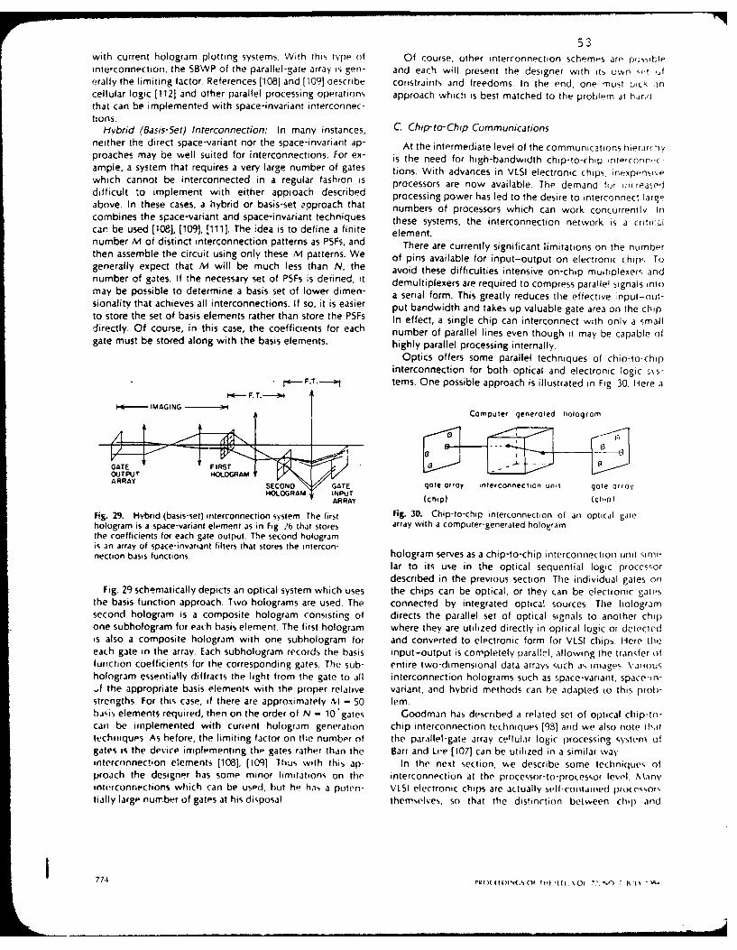
53with current hologram plotting systems, With this type of Of course, other interconnection schemes are posdiL e
interconnection, the SBWP of the parallel-gate array is gen- and each will present the designer with its own -t ,erally the limiting factor References [108] and [1091 describe constraints and freedoms. In the end, one must [,(' ,ncellular logic [112] and other parallel processing operations approach which is best matched to the problem at har~dthat can be implemented with space-invariant interconnec-tions.
Hybrid (Basis-Set) Interconnection: In many instances, C. Chip-to-Chip Communicationsneither the direct space-variant nor the space-invariant ap- At the intermediate level of the communications hierar iv
proachet may be well suited for interconnections. For ex- is the need for high-bandwidth chip-to-chip nterconn-,cample, a system that requires a very large number of gates tions. With advances in VLSI electronic chips, inexpensivp
which cannot be interconnected in a regular fashion is processors are now available. The demand for iwriadifficult to implement with either appioach described processing power has led to the desire to interconnect lafoeabove. In these cases, a hybrid or basis-set approach that numbers of processors which can work concurrently Incombines the space-variant and space-invariant techniques these systems, the interconnection network is a criti( lcan be used [108], [109], [111]. The idea is to define a finite element.number M of distinct interconnection patterns as PSFs, and There are currently significant limitations on the numberthen assemble the circuit using only these M patterns. We of pins available for input-output on electronic chips, Togenerally expect that M will be much less than N, the avoid these difficulties intensive on-chip multiplexer,, andnumber of gates. If the necessary set of PSFs is derined, it demultiplexers are required to compress parallel signals ntomay be possible to determine a basis set of lower dimen- a serial form. This greatly reduces the effective inpul-ouL-sionality that achieves all interconnections. If so, it is easier put bandwidth and takes up valuable gate area on the chipto store the set of basis elements rather than store the PSFs In effect, a single chip can interconnect with only a smalldirectly. Of course, in this case, the coefficients for each number of parallel lines even though it may be capable ofgate must be stored along with the basis elements, highly parallel processing internally.
Optics offers some parallel techniques of chip-lo-chipinterconnection for both optical and electronic logic sss-
-w. F.T.--, terns. One possible approach is illustrated in Fig 30. Here a
IMAGINGComuer generaed hologram
V G1
ARRAY GATE gate array interconnection unil gate ortoyHOLOGRAM INPUT
ARRAY (chip) (chip)
Fig. 29. Hybrid (basis-set) interconnection system. The first Fig. 30. Chip-to-chip interconnection of an optical gainhologram is a space-variant element as in Fig. 26 that stores array with a computer-generaled hologramthe coefficients for each gate output. The second hologramis an array of space-invariant filters that stores the intercon-nection basis functions. hologram serves as a chip-to-chip interconnection unit smi-
lar to its use in the optical sequential logic processordescribed in the previous section The individual gates on
Fig. 29 schematically depicts an optical system which uses the chips can be optical, or they can be electionic gatesthe basis function approach. Two holograms are used. The connected by integrated optical sources. The hologramsecond hologram is a composite hologram consisting of directs the parallel set of optical signals to another chipone subhologram for each basis element. The first hologram where they are utilized directly in optical logic or detectedIs also a composite hologram with one subhologram for and converted to electronic form for VLSI chips. Here theeach gate in the array. Each subhologram records the basis input-output is completely parallel, allowing the transfer offurnction coefficients for the corresponding gates. The sub- entire two-dimensional data arrays such as images Varioushologram essentially diffracts the light from the gate to all interconnection holograms such as space-variant, space-in-,f the appropriate basis elements with the proper relative variant, and hybrid methods can be adapted to this prob-strengths. For this case. if there are approximately AI - 50 lem.basis elements required, then on the order of N - 10'gates Goodman has described a related set of optical chip-lo-can be implemented with current hologram generation chip interconnection techniques [981 and we also note thattechniques As hefore, the limiting factor on the number of the parallel-gate array cellular logic processing system ofgates is the device implementing the gates rather than the Barr and Lee [107] can be utilized in a similar waymnterconnection elements [108], (109] Thus with this ap- In the next section, we describe some technique- ofproach the designer has some minor limitations on the interconnection at the processor-to-professor level. Nlan'interconnections which can be used, but he has a poten- VLSI electronic chips are actually self-contained processor"tially large number of gates at his disposal themselves, so that the distinction between chip and
77,1 PI (i(iXF NC, ',Oi o li Ii 1 .\01 1'.NO , IlO '

54
proce.or is no longer well detined. Many of tile pro.le,,,Ssor- owsbar swit( h contdins only binary entries, a Ir(prVi,,, .11-
to-processor interconnection chemes described-would also ing a conne(tion and a 0 implies no connection Thi- 'be valuable at the chip-to-chip level. inputs comprise the multiplying ve(tor and the N outputs
constitute the resultant vector. With a real-time de' jtoD. Processor-to-Processor Communications representing the matrix these systems become (dvnami(.
crossbar switches.At this highest level, a relatively smaller number of inter- Ao tia ite rk
connections are required, but they should have a very large ented by Taia et a. [124]. They use an optical ptem tO
bandwidth. Fiber-optics communication links are already connect a large number of processing units to a lrge
finding use in connecting computers with each other and number of memory unis They broadcast the sgnals o1 t-
with peripheral equipment. They provide high-bandwidth ally so that no wining s requiredt
links with good interference immunity, although they even-
tually suffer from the limitations of electronic buses in thatonly a small number of devices actively communicate at any V. ARCHITECTURES AND ALCORITHMStime and that processing overhead is required to implementprotocols. The use of optical systems, in particular highly parallel
In many instances where the processors perform a single systems, leads to certain implications in the design of com-function t-.. interconnection network itself defines the puting hardware. Some general comments about these ir.-operation. Thus a tree network (113] is used for sorting plications follow in this section. A similar hut some,,htprobiems and systolic networks (99], (100 are used for many different perspective is given by Huang [1251.matrix operations. The tree and systolic networks are gener- In the early days of computer development, the hardwareally fixed structures which perform a fixed operation. Ide- for both gates and for the gate interconnections was expen-ally, one would like to have a dynamic structure that could sive. Thus a computer design evolved which minimized thebe reconfigured to meet the users' needs. Such networks hardware requirements. These requirements have led to theare the subject of considerable research currently. classical von Neumann computing system architecture
A general-purpose dynamic network is the crossbar switch shown in Fig. 32. In a von Neumann machine, all of theshown in Fig. 31. This switch allows any of N inputs to be processing logic is contained in the 'central processing unit
(CPU) and the memory is located almost entirely in a
.. .. 1- -4MEMORY
N inputs
2N'swichesr/
N outputs Fig. 32. Von Neumann computer
Fig. 31. Crossbar interconnection network.
separate unit. Input-output is generally performed by theconnected to any of N outputs. Although this is the most CPU or by a system closely coupled to the CPU. The CPUgeneral switch one would normally need, it is seldom accesses the memory through a binary addressing unit andimplemented because of the large hardware requirements memory contents are returned to the CPU throu, gh a single(N switches). Instead, considerable research has been de- or small number of lines. This multiplexing scheme reducesvoted to devising simpler networks such as the Baseline the communications requirements snd minimizes the num-network (114], the Omega network [115], the binary n-Cube ber of lines. This serial addressing of memory results in anetwork (116], the Banyan network (1171, and the shuffle tradeoff of time for interconnection con-,plexit. The even-exchange network (118], [119]. These networks generally tual limitation on computing speed is known as the vonrequire less hardware than the crossbar network and also Neumann bottleneck. Current high-performance electronicprovide less performance. Since the crossbar and other computers operate with very short clock cycles, this meansnetworks are fixed for a given computation and are only that coaxial electronics with very short physical wire lengthschanged infrequently, the emphasis on implementing these are needed to avoid electromagnetic interference (EMI),systems is on parallelism or number of channels, rather than crosstalk, and dock skew problems. The coaxial electronicson speed. Optical approaches to implementing the crossbar for interconnections requires terminating resistors on thewould appear to be a viable solution to the interconnection ends of cables, further reducing system energy efficiencyproblem. In fact, optical systems which have been devel- With the development of integrated circuitry and iS1.oped for matrix-vector multiplication [1201-[123] are readily the situation has changed considerably. In VLSI, gates areadapted to function as crossbar switches. The "matrix" for a relatively cheap while communication lines are relatively
SAWCMUK AND STRAND DIGITAL OPTICAL COMPJriNG 775
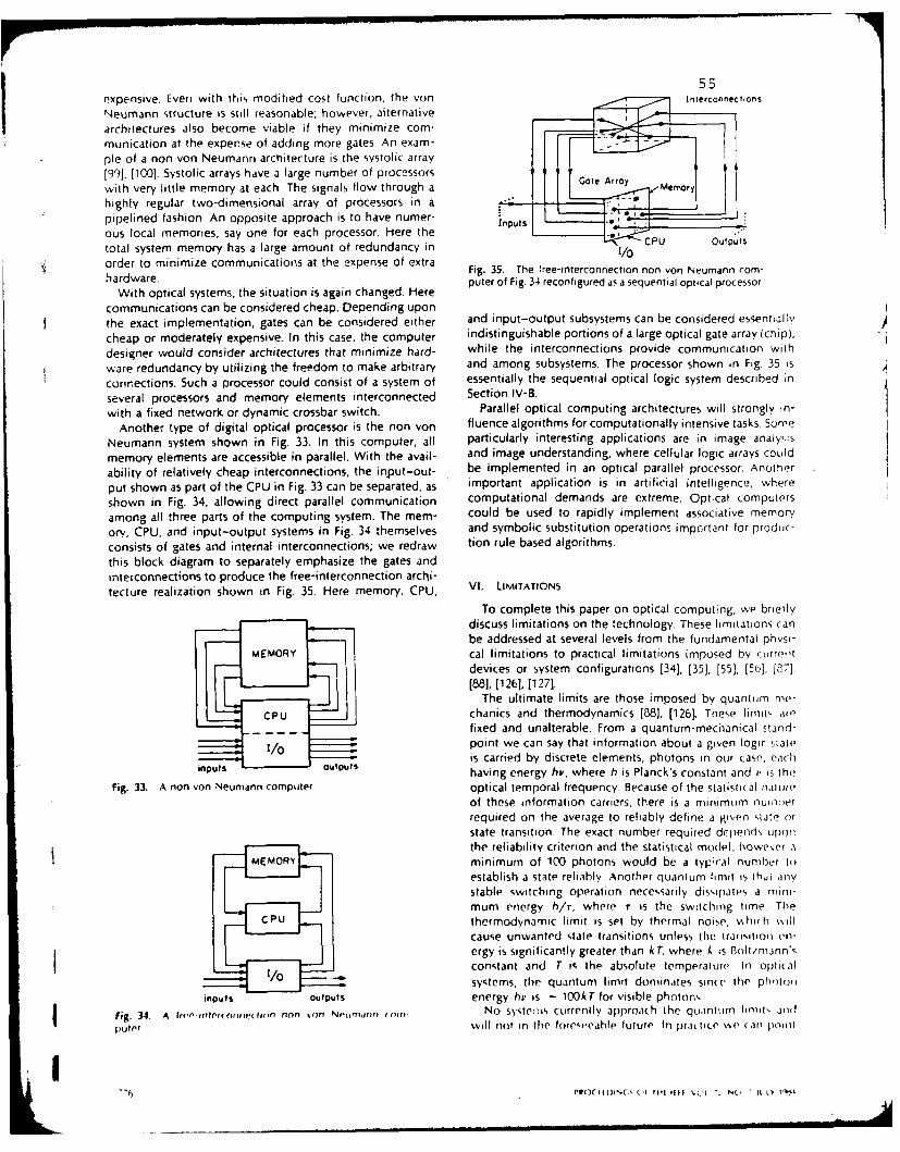
55
expensive. Even with this modified cost function, the von Interconnect-onsNeumann structure is still reasonable; however, alternativearchitectures also become viable if they minimize com-munication at the expense of adding more gates. An exam-ple of a non von Neumann architecture is the systolic array[991], [1001. Systolic arrays have a large number of processors ate Array
with very little memory at each. The signals flow through a Memor
highly regular two-dimensional array of processors in apipelined fashion An opposite approach is to have numer- ious local memories, say one for each processor. Here the Ouipuistotal system memory has a large amount of redundancy in 1/0
order to minimize communications at the expense of extra Fig. 35. The free-interconnection non von Neumann corm-hardware. puter of Fig. 34 reconfigured as a sequential optical processor.
With optical systems, the situation is again changed. Herecommunications can be considered cheap. Depending uponthe exact implementation, gates can be considered either and input-output subsystems can be considered essentalk,cheap or moderately expensive. In this case, the computer indistinguishable portions of a large optical gate array (chip),
designer would consider architectures that minimize hard- while the interconnections provide communication with
ware redundancy by utilizing the freedom to make arbitrary and among subsystems. The processor shown in Fig. 35 is
connections. Such a processor could consist of a system of essentially the sequential optical logic system described in
several processors and memory elements interconnected Section IV-B.
with a fixed network or dynamic crossbar switch. Parallel optical computing architectures will strongly n-
Another type of digital optical processor is the non von fluence algorithms for computationally intensive tasks. Some
Neumann system shown in Fig. 33. In this computer, all particularly interesting applications are in image analyo is
memory elements are accessible in parallel. With the avail- and image understanding, where cellular logic arrays could
ability of relatively cheap interconnections, the input-out- be implemented in an optical parallel processor. Another
put shown as part of the CPU in Fig. 33 can be separated, as important application is in artificial intelligence, where
shown in Fig. 34, allowing direct parallel communication computational demands are extreme. Optical computers
among all three parts of the computing system. The mem- could be used to rapidly implement associative memory
ory, CPU, and input-output systems in Fig. 34 themselves and symbolic substitution operations impcrta3nt for prodici-
consists of gates and internal interconnections; we redraw tion rule based algorithms.
this block diagram to separately emphasize the gates andinterconnections to produce the free-interconnection archi-
tecture realization shown in Fig. 35. Here memory, CPU, VI. LIMITATIONS
To complete this paper on optical computing, we brieflydiscuss limitations on the technology. These limitations canbe addressed at several levels from the fundamental phvsi-
MEMORY cal limitations to practical limitations imposed by currentdevices or system configurations [34], [35], [55], [Sb] i 7],
[881, [126], [1271.The ultimate limits are those imposed by quantum me-
CPU chanics and thermodynamics [83], [126. These limits are
fixed and unalterable. From a quantum-mechanical stand-
i/0 point we can say that information about a given logic slateis carried by discrete elements, photons in our case, eacth
iputl outputs having energy he, where h is Planck's constant and v, is thefig. 33. A non von Neumann computer optical temporal frequency. Because of the statistical nalie
of these information carriers, there is a minimum nurnerrequired on the average to reliably define a given stile orstate transition. The exact number required depends uponthe reliability criterion and the statistical model, howe.er a
MEMORY minimum of 100 photons would be a typical number toestablish a state reliably. Another quantum limit is thai dnystable switching operation necessarily dissipates a mini-mum energy h/r. where T is the switching time The
CPU thermodynamic limit is set by thermal noise, \,hiih vill
cause unwanted state transitions unless the tra ,iion en-ergy is significantly greater than kT, where k is Bolt.'mann*sconstant and T is the absolute temperature In optical
I/0 systems, the quantum limit dominates since the phuloii
inputs outputs energy hr is - lO0AT for visible photons
fig. 34. A fre"intr'rorire rin non von Neiriidtin rti No systei, s currently approach the quantum hm et', and
puter will not in the foreseeable future In pra(hce %(,e can poetl
neoc f il INC 1 i, il it[ \(it. -, N . It tR Vs

56
to other factors which currently set the limits on the perfor- Iportant prirnltiphe Iat O)ticdl co)rlpulers ioiul ,,ji
mance of optical logic systems. These limits are closely built by merely replacing electronic de,.ites wifi hi a
related to current device characteristics. A primary concern devices. Designing an optical logic 'ystem requires a H-\v
is heat dissipation, which is a severe problem because set of cost functions for trading off gale count and intir(n-energy consumption in practical systems far exceeds the nection complexity. These different design criteria ",ad to
quantum limits. Heat dissipation becomes a prublem when new architectures for logic systems and make optical implo-combined with the requirement of high gate packing densi- mentatloirs attractive "here cle( Ironic implenenldiOn'lies. In turn, the need for high gate densities is ultimately would be impractical. Designs which are interconnection
driven by time constraints on the communication intercon- intensive can often be easily mapped onto relatively simplenections. For optical logic systems based on absorption optical systems, whereas interconnection linutations arenonlinearities, heat dissipation is probably the limiting fac- already severely restricting VLSI design. Optical computingtor and optical systems compare unfavorably with elec- offers the possibility of non ,,on Neumann parallel architec-Ironic systems (34], (55], [56]. However, the situation may be tures with different mechanisms for interconnections anddifferent for systems based on reactive nonlinearities and communications; it remains a challenge to develop opticalresonant structures where absorption in the device is low devices, architectures, and algorithms that make use of thisand heat can be dissipated external to the logic elements potential. The next few years will be a critical and exciting[351, [881, [126!, (1271. It has been shown in the past few period for these technologies.years that liritations in this area are not fundamental, butrather are technology dependent, thus they can changedramatically with innovations in the field. ACKNOWLFDCNIENT
There are also practical limitations which are ied to theoverall system design. These are primarily communication The authors wish to thank B. K. Jenkins, P. Chavel, B. H.limits. the lengths of communication line, id the corre- Soffer, A. R. Tanguay, Jr., and R. Forchheimer fcr theirsponding signal transit times determine the r ,nimum cycle contributions to the research described in this paper.time. As discussed previously, communication limitationsfor optical systems differ significantly from electronic sys-tems. if one utilizes three-dimensional interconnection net- REFERENCESworks between planar gate arrays. However, the effectivedistance between planes still determines th- minimum cycle [1] 1. W. Goodman, Introduction To Fourier Optics. New York:time and should be kept as short as possible. For a given McGraw-Hill, 1%8.cmuiat shouldisektan, hoverthe ptsiclsstem s a e2] K. Preston, Jr., Coherent Optical Computers. New York:communication distance, however, the optical system has a McGraw-Hill, 1972, Ch. 8.faster minimum cycle time because communicating over [3] 0. Casasent, Ed., Optical Data Processmg-Apphcatron_electronic lines involves chargi.ng and discharging capaci- (Topics in Applied Physics, Vol. 23). Berlin: Springer-erlag,tances. 1978.
[4] S. H. Lee. Ed., Optical Information Processing-Fundamenrals(Topics in Applied Physics, Vol- 48). Berlin: Springer-Verlag
VII. FUTURE NEtDS AND CONCLUSIONS 1981.[5] H. Stark, Ed., Applications of Optical Founer Trafrsforn
In this paper we have reviewed optical logic elements New York: Academic Press, 1982.and digital optical computing systems. It is evident that [61 J. w. Goodman, "Operations achievable with coherent plti-cal information processing systems," Proc. YEEE, vol. ,5 p)iniuch more wor. is needed on basic research and develop- 29-38, 1977.rment efforts on both the devices and systems. [71 D. Casasent, "Coherent optical pattern recognition." Proc
We summarize here a few thoughts about desirable prop- IEEE. vol. 67, pp. 813-825, 1979.erties for optical logic elements. Devices with a fast switch- [8] E. A. Mnatsakanyan, V. N. Morozov, and Yu. M. Popov,
"Digital data processing in optoelectronic dvices (revrew),"ing time and low power consumption per bit are needed to Soy. I. Quantum Electron., vol. 9, pp. 65-677. 1979.be competitive with electronic devices. It is desirable to [9] G. HAusler, "Optical software survey," Opt. Acta., vol 24.
have input and output signals represented by the same pp. %5-977, 1977optical wavelengths to allow cascading of switching stages, [10] I. Jahns, "Concepts of optical digital computing-A ur'.eyi'
Opirk, vol. 57, pp. 429-449, 1980.and it is desirable to avoid photon-eIectron-photon con- [11] 1. W Goodman, "Architectural development of optical dataversions to improve switching speed and energy efficiency, processing systems," I Electrical Electron. Eng, Australa.A complete logical set can be achieved with NOR, NANO, vol. 2, pp. 139-149, 1982.and other types of logical elements (112b; all 16 two-variable [12] J. W. Goodman and H. B. Strrbin, "Increasing the d\namicbinary logic functions are probably not needed or wanted, range of coherent optical filters by means of modulatingEasy fabrication, high packing density, and room-tempera- gratings," ]. Opt. Soc. Amer., vol 63, pp. "0-58, 1973.
[13] R. P. Akins, R. A. Athale, and S. H. Lee, "Feedback in analcglure operation of arrays of devices is very desirable; these and digital optical image processing: A review." Opt Eng.
arrays must also allow easy nonplanar interconnections on- vol. 19, pp. 347-358, 190M.
chip and off-chip. A useful practical system that might be [14] D. Psaltis £t al., "Iterative color-multiplexed, electro-opticalconstructed as an optical computer is a parallel cellular processing," Opt. Left., vol. 4, pp. 348-350, 1979.
iprocessor for an image with 500 X 500 pixels (112]; [15] H. I. Caulfield et al., "Eigenvector determination by non-logic pcoherent optical methods," Appl. Opt., vol 20, pp 2263-such a processor might have 40 gates per pixel, or a total of 2265, 1981.107 gates. This number is not an unreasonable goal for a [16] 1. W. Goodman and M. Song, "Performance limitations of an
device array, analog method for solving simultaneous linear equatons."Appl. Opt., vol. 21, pp. 502-506, 1982At the systems level we have seen that optical computing [17W W. K. Cheng and H. I Caulfield, "Fully-parallel relaxation
srtems differ fundamentally from electronic systems. One algebraic operations for optical computers." Opt Conmmir.
C

Niol 43. pp. 251-254, 11982, 368-38, 1960. 5[161 11. L Garner. " Thp residue number s"Item', IRE Trans. Eleu (471 A B Fowler, "Quenching or gillurn drw'i'r- ,
Comp, vol EC-8. pp t40-147, 1959) lasers," Appi. Phys. Lett, soil 3 p 1, 063[in] A Pasaki, "Addition and subtraction in the residue number f481 , "Cooperative effect tn GaAs lasers, I Appi h~
ss'tem," IEEE rrans Elect Comp., sal tC-1b. pp. 137-1o4. vol. 35, pp. 2275-2276, 1%41967 [491 C I. Lasher and A B Fowler '\1utuaIy cluenc.h-i njIi;-fn
[201I N S Szabo and R I Tanaka. Residue Arithmnetic and Its lasers as bistable devices'" 18.5. / Res Oielu) )pApplications to Computer Technology New York: Mc- 471-475, 1%4Craw-Hill. lb7 (501 C I Lasher. "Analysis of a proposed bistable nir-i non lam-r.'
[-'I A. Huang. "The implementation of a residue arithmetic utlit Solid'Stite Electron. vol 7, pp 707-716, 1%4via optical and other physical phenomena," in Proc. 1975 Int [511 M. 1. Nathan et a/,, "GaAS injection laser with novel modeOpt Comp. Cornt (Washington. DC, Apr 1975), pp. 14-18. control and switching properties," I. AppI P/-ps , sol 11b, pp.
1221 S. A Collins, Jr., "Numerical optical data pros essor," Proc. 473-480, 1%5.Soc. Photo-Opt. inst Eng.. vol 128. pp. 313-1''), 1977. [521 0. A. Riemann and W F Kosonixky. "Progress tn iiptiai
231 S. A. Collins, Jr., 1. Ambuel. arid E. K. Damon. "Numerical computer research," IEEE Spectrum, \sol 2. pp 181-195, 'Ovioptical data processing," in Proc. 1978 Int Opt. Comp. Cant. 1%5(London, England, Sept. 1978), pp. 194-197. [531 W. V. Smith. "Computer applications of lasers," Proc. IEEE.
(241 - , "Optics for numerical calculation," in Proic. ICO-I I vol. 54, pp. 1295-1300. 1*6Conif. (Madrid, Spain, 1978), pp. 311-31-1. [541 N. C. BaSOV. W. H. Culver. and B. Shah, in Laser Handbook.
(251 0. Psaltis and 0. Casasent. "Optical residue arithmetic: A F. T_ Arecchi and E. 0. Schulz-DuBois, Eds Amnsterdlamcorrelation approach," Appif Opt., vol. 18, pp. 163-1 71, 1 q79. North-Holland. 1972.
1261 F A. Horrigan and W. W Stoner, "Reidcue-based optical [55] R. Landauer. "Optical logic and optically accessed digitalprocessor." Proc. Soc. Photo-Opt. Inst. Eng., vol. 185. pp. storage," in Optical Information Processing. Yu0. E. Nesterik'19-27, 1979. hin, et al., Eds. New York: Plenum, 1976, pp 219-253,
[271 A. Huang, Y. Tsunoda, ). W. Goodman, and S. Ishihara, (561 R. W. Keyes, "Power dissipation in information processing.""Optical computation using residue arithmetic." AppI. Opt., Science, vol. 168, pp. 7%--801, 1970.vol. 18, pp. 149-162, 1979. [57] N. G. Basov el a)., "Methods of realization of an optical
[281 A. Huang and 1. W. Goodman, "Number theoretic processors, processor with variable operators,' Sac /. Quantum rfec-optical and electronic," Proc. Soc. Photo-Opt. Inst. Eng., vol. tron., vol. 8, pp. 307-31 2, 1978185, pp. 28-35, 1979. (581 C. C. Guest and T. K. Gaylord, "Two proposed holographic
[291 A. Tai, 1. Cindrich, 1. R. Fienup. and C. C. Aleksoff, "Optical numerical optical processors," Proc. Soc. Photo-Opt Inst.residue arithmetic computer wo 'th programmable computa-. Eng., vol. 185, 1979.tion modules," AppI. Opt., vol. 18, pp. 281 2-2923, 1979. (591 A. Seko and M. Nishikata, "Image emission platelet laser for
[301 C. C. Guest and T. K. Gaylord, "Truth-table look-up optical optical information processing," AppI. Opt, vol. 16. ppprocessing utilizing binary and residue arithmetic," App. 1272-1 274, 1977.Opt., vol. 19, pp. 1201 -1 207.,1980. [601 A. Seko and A. Sasamori, "Fiber laser plate," AppI. Opt., vol.
(3 t] S. 0. Fouse et it., "A residue-based image processor for VLSI 18, pp 2052-2055, 1979.implementation," in Proc. Image Understanding Workrshtop, [611 A. Seko, "All-optical parallel logic operation using fiber laserL. Baumann, Ed., DARPA/Science Applications, Inc., Rep. plate for digital image processing," AppI. Phys Left , vol. 37,SAI'82-391-WA. pp. 188-198, Apr. 1981. .pp. 260-262, 1980.
[321 5. 0. Fouse, G. R. Nudd, and A. D. Cummings, "A VLSI (621 A. Seko, H. Koba'yashi, and K. Shimizu, "A high-speed imagt,architecture (or pattern recognition using residue arithmetic," information preprocessor using a channel plate imag.- in-in Proc. 6th tnt. Cant. on Pattern Recognition (Munich, tensifier," Opt. Eng., vol. 19, pp. 229-232, 1980.Germany, Oct. 19-22, 1982). IEEE 82CH1801-0, IEEE Comp. [631 B. M. Watrasiewicz. "Optical digital computers." Optir"Sec., pp. 262-269 Laser Technol., vol. 7, pp. 213-215, 1975.
[331 8 K. Jenkins et al., "Sequential optical logic implementa- (641 V. A. Tsvetkov. N. A. Morozov, and M 1. Elinson, "Picturetion," submitted to App. Opt. logic and liquid crystals," Soy /. Quint rI'ectron. of 6,. pp
[341 R. W. Keyes and I. A. Armstrong, "Thermal limitations in 9839-993, 1975.optical logic," Appi. Opt.. vol. 8, pp. 2549-2552.,1%9. (651 D. H. Schaefer and I P. Strong. III, "Tw. computer, ' ('mc
[351 - , "Fundamental limits in digital information process- IEEE, vol. 65, pp 129-138.,1977.ing," Proc. IEEE, vol. 69, pp. 267-278, 1981. [661 S. H. Lee, "Review of coherent optical processing," App/
(361 L. C. West, "Construction of a general purpose digital com' Phys., vol. 10, pp. 203-21 7, 1976.puter based on optical logic elements," in CLEO Tech. Dig., [671 R. A. Athale and S. H. Lee, "Development of an optialpaper TUGS, Opt. Soc. of America, p. 44, may 1983. parallel logic device and a half-adder circuit for digital opli-
[371 C Mead and L. Conway, introduction to VLSI Systems. cal processing." Opt Eng. vol 18, pp 513-517, 1479.Reading, MA: Addison-Wesley, 1980. [681 - , "Bistability and thresholding by a new photnwonduc'
[381 T. Tamir, Ed., Integrated Optics, 2nd Ed. (Topics in Applied tar-twisted nematic liquid crystal device with optical fee'd-Physics, Vol 7) Berlin. Spiringer-Verlag, 1981. back." AppI. Opt., vol. 20. pp. 1424-1432. 1981.
[391 H F Taylor. "Guided wave electra'aptic devices for logic [691 1. Michaelson, "Characterization of liquid Crystail lightlsearid (amputation." AppI Opt, vol 17, pp. 1493-1498, 1978. and their applications, to real-time nonlinear optical proc's'.
[4301 L Goldberg and S. H Lee, "Integrated optical half adder ing." Ph.D. dissertation. Dep. Elec. [rig, Univ of So Calit,circuit." AppI Opt.. vol 18, pp. 2045-2051. 1979. Las Angeles, Oct 1979; USCIPI Rep 930, USC Inmage Prot i's'.
[411 C. H Bulmer. W. K. Burns. and T. C. Giallorenzi, "Perfar' ing Inst.. Los Angeles. CA 90089. 1979mance, criteria and limitations of electrooptic waveguide [70] C. Warde, A M. Weiss. A 0. Fisher. ind I I Thackara.array def lectors." Appi Opt., vol 18, pp 3282-3295, 1979, 'Optical information processing charatr'itets nf ti', iii to
1421 R A Becker and W S C. Chang, "Electrooptical switching in channel spatial light modulator" Appi Opti, sol '0, 1Wlthin film waveguides for a computer communications bus." 2066-2074. 1981.Appi Opt. vol 18, pp 32%6-3300, 1979 [1[1 M. T. Fatehi, K C Wasmuirdt, and S A Collins. Ir."ift(t
[Jail C. Verber, "Integrated Optical Architectures and imple- logic gates using liquid crystal light %alve tmllrtmaii~nmentation," Proc. SPIE, vol 456. 1964 and application i'sanple," Appf Opt . vol 20. lPp 2250.-'251,
[441 1. von Neumann, "Non-linear capacitance or inductance 1981switchin~g, amplif~ing and memory organs," US Patent 2 815 [7211 H. Bartell and A. 5.V Lohmanno "Hybrid logu pr.o"""nK in488. 1954, parallel." AppI Opt , vol 22. pp. ?519-2520. 11183
(451 E Goto. "The parametron, a digital computing element [731 1 o Armitige and A VVI lnhrn,- Iheta miidulation inw~hich utilizes parametric otiollatinns," Proc IRE, vol .17, pp opti 5." Appi Opt. sol 4, p 399. '5513104-1316, 1959 1741 I Tanida aind V k hiok a, '01 i ii i logic(( pro.r'ai r inGt' Diemer andl G. Van Santen, "Power amplifiers based on Proc Ifft t'1f3 l0th tnt Opt Comup Coot, pp) 4k2.. ,)r
.'lectrn-npttral efi'ts." Philips Rt's Rep. %nI 15, pp 18
718P 0HI..0 11, M % k* o *lt ,A

587I7 Tanirda nd Y Ictuoka, Optical logic array piocesor using C-31, pp 1054- 1(-o. 1982
.tadowgiams. I. Opt o0c Amer, vol 73, pp ,0' X-809. 11021 A Armand e( ,. Realtrme paralleli ptiial an.io-ti-',iiJr-d 3. (onversi.on," Opt. Leftt, ,ol 5, pp. 129- 131, 1 QM
17r - ."Image entoding by a computer generated holo- [1031 R, K. f ai and D. E. Sivdr. pAddrps1, ind (.ontrol ,AI
graphc tillr.' Pro- PI'. kol 432. 1983. high-speed logic cir(uits with picosecond light piulses, ' ('7t17-1 A A Savichuk. T C. Strand. and A. R. Tanguas. Jr , "Nonlin- Lett., vol. 3. pp. 335-d7, 1983.
eai Teai-tiire otir al sgnal proces ,mg. ' USCIPI Rep 1080, [1041 M, T fatehi et al.. "Sequential logic element irrdvs tor uo n
USC Imag' Prnoe', ng Inst . Los Angele-. CA 4-.)89, 182. optical digital processor,. Applications and Ilmitations,' i'mi
17, "- Nnline.;r rwal-time opi(al signal processing," SPIE, vol. 241, pp. 139-148, 1980.
UjClPI Rep 1100. 1.S(- Image Processing lost , Los Angeles. [105] G. Ferrano and G. Hiusler, "A bistable TV-opti al fe"-ha( k
CA riqi . A r'!3 system," Opt. Commun. vol. 32, pp 375-379 in80[7c I I Grint.wrv, ,f itl. A r,,,. real-time nuncoherent to coherent [1061 G. Ferrano and G. Hausler, "TV/ optical fepedhack swm,,,
orptical ,rnte (onver'r. Opt Eng, vol 14, pp. 217-275, Opt. Eng., vol 19, pp. 442-451, 1980.10-5 [1071 11. Barr and S. H Lee, "A digital optial processing bhk'm.
ItIC) I Ginhg t it.. "Phlotoactiated birefringent liquid-crystal in Prec. 10th Int. Optical Computing Coi. pp. 71 -:-hIelt a~ve ilr color symbologv display," IEEE rrans. Electron IEEE Cat. 83CH1880-4, IEFE Computer Soc , Si'er Spriig, %.4),Do,.','s. vol ED-22, pp. 775-783, 1975. 1983.
ei) i,% j, Bleha et il, "Application of the liquid crystal light (108] P. Chavel et ai., "Architectures for a sequential optical liiSal'.' to real-time optical data processing," Opt. Eng., vol. 17, processor," in Proc. 10th Int. Optical Computing Cori. pppp 371-384, 1978. 6-12, IEEE Cat. 83CH-1880-4, IEEE Computer Soc. Silver Spring,
1921 a H. Selter et Al., "Variable grating mode liquid crystal MD, 1983.tievire tor optical processing and computing," viol, Cryst. [1091 B. K. Jenkins et al., "Architectural implcations of digital
Lip Crs-t, vol. 70. pp. 145-161, 1981. optical processors," submitted to Appl. Opt.[831 P Chavel, A. A. Sawchuk, T. C. Strand, A. R. Tanguay, Jr., and [110] W. H. Lee, "Sampled Fourier transform hologram generated
B. H Softer, "Optical logic with variable-grating-mode liquid by computer," Appl. Opt., vol. 9, p. 639. 1970crystal devices," Opt. Lett., vol. 5, pp. 398-400, 1980. [111] B. K. Jenkins and 1. C. Strand, "Computer generated holo-
(84[ P %V. Smith, E. H. Turner, and P. 1. Maloney, "Electrooptic grams for space-variant interconnections in optical logicnonlinear Fabry-Perot devices," IEEE]. Quant. Electron., vol. systems." in Proc. Int. Con,. on Computer Generated Holoq-QE-14, pp. 207-212. 1978. raphy, 5PIE Proc., vet. 437, pp. 110-118, 1083.
[,51 E. Garmire, S. 0. Allen, and J. Marburger, "Bistable optical (112] K. Preston et at., "Basis of cellular logic with some appica-devices for integrated optics and fiber optics applications," lions in medical image processing," Proc. IEEE, vol. 67. ;)pOpt. Eng., vol. 18, pp. 194-197, 1979. 826-856, 1979.
[&,] P W Smith, "Hybrid bstable optical devices," Opt. Eng., [1131 L. Snyder, "Introduction to the contigurable, highly parallelvol. 9, pp. 456-462, 1980. computer," IEEE Computer, vol. 15, no. 1, pp. 47-58, 1982
187] H M. Gibbs, S. L. McCall, and T. N. C. Venkatesan, "Optical [1141 C. Wu and T. Feng, "On a class of multi-slage interconnec-bistable devices: The basic components of all-optical sys- lion networks," IEEE Trans. Comput., vol. C-29, pp. 694-702.tems?" Opt. Eng.. vol. 19, pp. 463-468, 1980. 1980.
[881 P W Smith and W. I. Tomlinson, "Bistable optical devices [115] 0. H. Lawrie, "Access and alignment of data in an airaypromise subpicosecond switching," IEEE Spectrum, vol. 18, processor," IEEE Trans. Comput., vol C-21, pp. 1145-1155no. 6, pp. 26-33, June 1981. 1975.
fqj C. ,M1 Bowden, M. Ciltan, and H. R. Rob), Eds., Optiral [116) M. C. Pease, "The indirect binary n-cube microprosso(r6itablity. New York: Plenum, 1981. array," IEEE Trans. Comput., vol. C-26, pp. 458-473, 1977
1901 E. Abraham, C. T. Seaton, and S. 0. Smith. "The optical [1171 L. R. Goke and G. J. Lipovski, "Banyan networks for paoi-computer," Scienti. Amer., vol. 248, no. 2, pp. 85-93, Feb. tioning multiprocessor systems," in Proc. Ist Ai iu. 5yinp in1983 Computer Architecture, pp 21-28. Dec. 1973.
[911 I. L. lewell, M. C. Rushford, and H. M. Gibbs, "Use of a [1181 T. Lang and H. S. Stone, "A shuffle-exchange netwoik with,,ingle nonlinear Fabry-Perot etalon as optical logic gates," simplified control," IEEE Trans. Comput., vol C-25. pp. 55-t5Appi Phys. Let., vol. 44, pp. 172-174, 1984. 1975.
1921 Digest of Papers (Topical Meeting on Optical Bistability, (1191 H. S. Stone, "Parallel processing with the perfect shuffl.Rochester, NY, June 183), Opt. Soc. of America, Washing- IEEE Trans. Comput., vol. C-20, pp. 153-161, 1971.
Con. DC, 1963. [1201 R. A. Heinz et al., "Matrix multiplication by optical method<.,1931 I. A. O'Brien, "Bi-stable image storage apparatus," US Patent Appl. Opt., vol. 9, pp. 2161-2168, 1970.
3 941 455, Mar. 2, 1976. [1211 R. P. Bocker, "Matrix multiplication using incoherent optic(al[941 U. K Sengupta, U. H. Gerlach, and S. A. Collins, Jr., "Bistable techniques," Appl. Opt., vol. 13, pp. 1670-1676, 1974.
optical spatial device using direct optical feedback," Opt. [122] J. W. Goodman et al., "High-speed incoherent opticalLett., vol 3, pp. 199-201, 1978. method for performing discrete Fourier transforms," C:t
1951 U. H. Gerlach, U. K. Sengupta, and S. A. Collins, Jr., Lett., vol. 4, pp. 1-3, 1978.' Single-spatial light modulator bistable optical matrix device [123] R. A. Athale, "Optical matrix algebraic processors: A survi'viusing optical feedback," Opt. Eng., vol. 19, pp. 452-455, in Proc. 10th Int. Opt. Comput. Cnt, IEEE Computer Soc.1980. Press, pp. 24-31, 1963.
[96) S. A. Collins, Jr. et al., "Multi-stable optical system," US [124] H. Tajima, Y. Okada, and K. Tamura, "A high speed opticaiPatent 4 272 157, June 9, 1981. common bus for a multi-processor systems," Trans in',t
[97[ D. F. Barbe, Ed., VLSI: Fundamentals and Applications. Electron. and Commun. Eng. of Japan, vol. E66, pp a--3.Berlin: Springer-Verlag, 1982. 1963.
1981 I. W. Goodman, "Optical interconnections in microelectron- [125] A. Huang, "parallel algorithms for optical digital computer's,ics," Proc SPIE, vol. 456, Jan. 1984. in Proc. 10th Int. Opt. Comput. Con., IEEE Computer Sot.
[99] H. T Kung and C. E. Leiserson, "Syctolic arrays (for VLSI)," in , Press, pp. 13-17, 1983.Sparse Matrix Proc. 1978 (Soc. for Industrial and Applied [126] P. W. Smin, "On the physical limits of digital optical w,i h-Mathematics), pp 256-282, 1979. ing and logic elements," Bell Syst. Tech. I., vol 61, pp
1001 H. r Kung, "Why systolic architectures, IEEE Computer, vol. 1975-199., 1982.15, pp. 37-46, 1982. [127] R. L. Fork, "Physics of optical switching," Phys. Rev A .vol
11011 S Y Kung et al, "Wavefront array processor- Language, 26, pp. 2049-2064, 1982.architecture, and applications," IEEE Trans. Comput., vol.

1.3 Variable Grating Mode Liquid Crystal Devices
The variable grating mode (VGM) liquid crystal device has
been further studied experimentally [4-16]. This work has been
in conjunction with the device development work being done at
Hughes Research Laboratories.
An important area of research on the Variable Grating Mode
Liquid Crystal Light Valve is concerned with a fundamental
understanding of the origin of the "variable grating" effect. A
wide variety of studies have been performed on electrically
addressed VGM cells (no intervening photoconductive layer), in
which diffraction order polarization and intensity were measured
as a function of input polarization and applied cell voltage and
the results correlated with observations of the VGM structure
under polarized illumination in a polarizing microscope, as well
as the with various theoretical models of the VGM domain
structure.
Three recent papers summarizing these results are included
here. The first paper "Physical Characterization of the Var:able
Grating Mode Liquid Crystal Devi e" by A.R. Tangua,,, .,
C.S. Wu, P. Chavel, T.C. Strand, A.A. Sawthuk, anc B.H. Soffe: ,
has been published in Optical En( ineering, s5n9:a" ss- I
Spatial Light Modulators: Fundamental Chara"':-'t
November/December 1983. This paper summarizes the phys,
principles of operation of VGM devices and describes work in: ,i
experimental measurements of the Jones matrix des."rib~r.;
!
60
polarized light propagation through the VGM cell; b) tne
thickness dependence of the molecular orientation angles; :
understanding of the physical constraints on the VGM response
time; and d.) the possibility of a VGM device with ac bias.
A second paper "Polarization Properties of the Variable
Grating Mode Liquid Crystal Device" by A.R. Tanguay, Jr.,
P. Chavel, T.C. Strand, C.S. Wu, and B.H. Soffer, has been
published in Optics Letters and is also included here. Tnis
paper contains detailed results on the spatial distribution of
the orientation of liquid crystal molecules in a VGM device.
Experimental measurements of the polarization properties of light
diffracted by the liquid crystal birefringent phase grating have
been made as a function of the applied voltage across the cell.
A final paper, "Intensity-to-Spatial Frequency
Transformations in Optical Signal Processing," by A.A. Sawchur,
T.C. Strand and B.H. Soffer describes applications of VGM devices
to perform optical nonlinear transformations and logiz
operations.

I m.. .II
61
Physical characterization of the variable grating modeliquid crystal device
A. R. Tanguay. Jr. Abstract. The physical principles of operation of the variable grating mooeC. S. Wu (VGMI liquid crystal device are described The VGM device is capable of per-P. Chavel" forming a two-dimensional intensity-to-spatial frequency conversion, which inT. C. Strandt turn allows the implementation of a wide range of nonlinear optical processingA. A. Sawchuk and computing functions The device utilizes certain nematic liquid crystalUniversity of Southern California mixtures that are observed to form variable frequency diffraction gratings unaerImage Processing Institute, and Departments of the influence of an applied bias voltage. Both fundamental and technological
Electrical Engineering and Materials Science limitations to device performance characteristics are discussedLos Angeles, California 90089-0483
Keywords spatial light modulator, variable grating mode. liquid crystal device oprca/B. H. Softer Information processing, optical devices
Hughes Research Laboratories Optical Engineering 22(6), 687-694 (November December 1983)3011 Malibu Canyon RoadMalibu, California 90265
CONTENTS The sariable grating mode liquid crystal device (\GM I CD rtransforms input intensities to spatial positions w hen used in coniunc-I Introduction ton with a Fourier transform lens. The nature of this image trans-
2 Device description and operational mode formation can be realized in the lolloswing manner The 's (M .(1D3 Fundamental origins of the operational properties primaril. consistsof a photoconductive layer in series with a laxer oi4 Physical origin of the ,ariable grating mode effect nematic liquid crystal mixture. A dc bias % oltage is applied acros the5, Acknowledgments device to pro% ide a voltage di\ ision between the two la\ ers. 'ithina6 References given image pixel, the input intensitY decay s the \ oltage across the
!. INTRODU'CTION photoconductive layer and correspondingl, enhances the soitageacross the liquid crystal layer. The photoconductor thus implements
A side %ariety, of one-and two-dimensional operations are necessary an intensit.-to-,oltage conversion. The nematic liquid cr\ ta, mix-for full-scale implementation of parallel optical processing and ture employed in the device has the unusual propert\ that ,hecomputing systems. Incoherent-to-coherent conversions are often alignment of the liquid crsstal molecules. which is homogeneouN inrequired for algorithms involving spectrum analysis and modifi- the quiescent state, exhibits spatiall\ periodic modulation ,when acation, correlation. conolution, and holographic image formation, bias voltage is applied across the laver. This modulation results in aparticularly when the information to be processed is a.%ailable only in birefringent phase grating,' characterized by a spatial trequenc\ thattime-sequential or matrix-addressed raster format. A number of depends linearly on the applied voltage. The effect ot the liquidone- and two-dimensional spatial light modulators capable of this crystal laver is thus to implement a voltage-to-spatial trequenc\tspe of image transduction at. iescribed within this special issue of conversion, If both lasers are considered together, the entire de% ice isOptical Engineering.'-" as well as in several review articles.' I thus seen to perform an image-wise intensity-to-spatial frequent.
Other. equally important processing and computing functions, consersion. which can be modified to the more general intensits-to-such as logic operations. programmable matrix addressing, binary position transformation by placing a Fourier transform lens behindaddition, linearity compensation, and input-output nonlinearities the VGM LCD. Collimated readout illumination normally incident(e.g.. exponentials, logarithms, power laws. thresholds. level slices, on the device (at a wavelength of photoconductive insensitisit\ I isand level restoration), have proven particularly difficult to implement. angle encoded within each image pixel b\ diffraction from eachAll of these functions, on the other hand, can be implemented by induced phase grating and subsequently angle-to-position mappedmeans of some form of intensity-to-position encoding in conunction by the Fourier transform lens into its focal plane.w4ith either fixed (single function) or programmable (multifunction) This type of process is shown schematically in Fig. 1. in which themasks. This general statement follows from the realization that all of input image is assumed to consist of two separate regions of differingthe functions listed above are special cases of data-dependent multi- intensity The VG1M I CD encodes both regions with different spatialplications. in which the input value (e.g.. pixel intensity) selects the frequencies, resulting in separated diffraction orders in the filterappropriate multiplier (e.g.. mask location) to obtain the desired (Fourier) plane Insertion of an appropriate spatial filter or pro-product (e.g.. output ntensity). grammable mask (not show n in Fig. I) into the Fourier plane allows
the separated orders to be selectisely modified to implement anv
* Permanent address Institut dnOptique .Iniertie de Pari% skid. RP 41 41406 O r r.t desired data-dependent multiplication or point nonlhnearit\ In the(edet. France reconstructed output image. all regions of equal input intensit\ are
*Present address IBM (orporation. 560) Collie Rd . San Jtse. ('A 01 modified identically irrespectie of their location in the input imagefield. Ihus. all of the data-dependent multiplications are performed
nin parallel Functional programmabilit\ is achieved hv replacementIn~ited Paper l M-IO4 recei'.ed Jul%. 15, Iqfil. re,.iscd manus.cript recei' ed Jul\ 'K. 1I"
acceptedforpubhication aug -. 193. receised h% Managing Fditor Atug 29 1991 this or reprogramming of the Fourier plane mask. which need onls be apaper is a reviion oi Paper 198-12 .hich ,as presented at the SPIF c.onerence on los" resolution device sith a total nurber of resolution elementsAdances in Optica Information Processing. Jan 2021. 195I. 1 o% Angeles, (,A theaper presented there appear% iunrelereedi in pit Proceedings oi Ass equal to the number of gra, levels required to be processedS481 Societs. of Phoio-i)ptcal Instrumentation F ngineers the oserall Input-output characteristic of nonlinear function
OPTICAL ENGINEERING November December 1983 Vol 22 No 6 687
Lt

TANGUAY WU CHAVEL. STRAND SAWCHUK SOFFER 62
.- ".QA 2'Q." m 25
Fig 1. Experimental arrangement for demonstration of intensity-to-position encoding by means of an intensity-to-spatial frequency conver-sion in a VGM LCD.
,re, -. GM
: . .c
-'e' - onhner i
Outpui
intensity
Fig 2 VGM nonlinear proceshing The overall input-output characteris-tic can be found by stepping through the successive nonlinear transfor-mations, including Ill the intensity-to-spatial frequency conversion. (2)spatial filtering, and 13) intensity detection. (b)
.mplementation utili;ing the VGM LCD is shosn schematicaly in Fig. 3 Polarization photomicrographs of the liquid crystal domain pat-Fig 2 bs specil.ing sequentiallp the nature of the transformations tern in an electrically activated cell. In (a), the polarizer was oriented atfrom input intensitt to spatial trequency sithin the VGM LCD. from 90-. and the analyzer at 90 . with respect to the grating wave vector Inspatial trequenc to spatial tilter amplitude transmittance in the (b), the polarizer was oriented at 90'. and the analyzer at 10 withFourier transform plane. and from output amplitude to output respect to the grating wave vector. The unit vector A(IA denotes theintensits I usually b means of square lass detection). The oxerall direction of quiescent alignment, and kG indicates the direction of the
nonlineari. achiesed can be easily compensated for the functional grating wave vector.
dependence. ot the separate steps bN adjustment of the selectedspatial filter transmittance function
The %G(M I U'D has thus far been utilized to perform a sside of these concepts has appeared presiously.%an etp o parallel nonlinear point transformations, including lesel The critical element of the VGM 1.CD is a thin 14 to 12 im) la\erslicing 'hinarN logic functions (AND. OR. NOR~etc.I,11 '-andlull hin r .tddition tinput s I Aso addend bit planes and one carre bit of nematic liquid crstal mixture!- that exhibits a periodic modulation
of the liquid crstal director, and hence of the index ellipsoid, inderplane. outnuts sum bit plane and carr bit plane).'' The purpose of application of an electric field normal to the plane ol the la\er B\this paper is i describe the phsical principles of operation of the mans of suitable preferental algnment techniques: the quiescentariable grating mode liquid crstal des ice. identifs areas ol strength state of the liquid cr stal is homogeneous (parallel to the plane f the
and bkeakness. and differentiate limitations to current device per- laverl As \kill be discussed in Sec 4 this periodic aTlatlon ot thetormance thought to be fundamental in origin from those that are principal axes o the dielectric tensor gises rise toa biretringent phaseseeminglp technological Section 2consistsof a more detailed descrip- grating characteried bp striking and unique optical propertiestion of the de,ce. its operating mode. and its operational properties ihe grating can be isualied a polarizing microscope, as ho in
The fundamental origins of these operational properties are examined Fig 3. b, utilizing the birefringence properties of the periodic per-In Sec S . in, ihich the natural focus %ill be the ph~sical mechanismot turbation Distinct polarizer analofer combiatons gise rie ti
the ,ariale grating mode effect in nematic liquid crn.stal mixtures. remarkahlN different grating images, as can be seen bs comparison oiExperimental and theoretical efforts to elucidate the nature of this Figs 3(a) and 3(b) (see Sec. 4). Furthermore, the grating period i,mechanism are described in Sec 4, sshich concludes %kith seseral obsersed experimentalp to be related insersely to the applied olitageimportant but as set unanssered questions. across the laver Abos.e the threshold for domain formation. there
fore. the spatial frequenc% of the grating is a linear function ol the2. DEVICE DESCRIPTION AND OPERATIONAL MODE %oltage across the laser, as shobkn for a sariets of nematic liquid
A number of important aspects of de% ice construction and deu' ce crystal mixtures in Fig 4operation are re% tewed in this section A more complete description I his s oltage-lo-spat al requencs transformat In can he optil Is\
688 OPTICAL ENGINEERING November December 1983 Vol 22No 6

PHYSICAL CHARACTERIZATION OF THE VARIABLE GRATING MODE LIQUID CRYSTAL DEVICE
6o ~ 2N4,D 9T
a 2N40 E_L A
o 2N40 CE._ E2N42 C' 2%42 CE-
8 2NII CE-L
500- *2N25 CE_- I "
x 2N45 EN.2Nil + MERCK NPV -
MERCK NPv
40- '- iz 0- -N43
2N25_Fig. 5. Schematic diagram of the VGM liquid crystal device. Current
ul devices are read out ifl transmission at a wavelength of photoconductiveZ insensitivity.
3. FUNDAMENTAL ORIGINS OF THE OPERATIONALPROPERTIESAs was mentioned in Sec. 2. the operational properties of the \ GM
2- X/ LCD are primarils determined b , the sariable grating mode ettectexhibited by the nematic mixture liquid crystal laer. The current stateof knowledge concerning the physical origin of this unique effect ;s
X summarized in Sec. 4. In this section. we outline a number ot kes2N42 factors and considerations that affect seseral important deuice prop-
erties in order to provide both focus and a frame of reference for the10 _ ___ succeeding section. These des ice properties include the accessible range0 20 40 60 80 C30 12C of spatial frequencies, the number of accessible gray lesels. the tunc-
tional dependence of diffraction efficiency on applied ,oltage. maxi-APPLIED VOLTAGE, VOLTS .DC mum diffraction efficiencs. response time. desice uniformit. de,.ice
Fig 4 VGM spatial frequency as a function of applied voltage for various input sensitiiity. and des ice operational lifetime.nematic liquid crystal mixtures. The accessible range of spatial frequencies extends from the thresh-
old for grating formation at the low end to the onset of dynamcscattering induced by high electric fields at the high end. as shown inFig 4. For phensl benzoate mixtures with slightly negatise dielectric
addressed h% means of a photoconductor placed in series with the anisotropy ( <-0.30) such as HRL 2N40.5 this range extends tromliquid cr5,stai laser. as show n in Fig. 5 and described in the prexsou, approximately 200 line pairs mm to oser 600 line pairs mm. In ordersection The photoconductise laser emplosed in devices constructed to asoid o\erlap of higher diffracted orders from lower spatial fre-thus tar is comprised ot eaporated or ion-beam sputtered zinc sullide quencies with lower diffracted orders from higher spatial trequencies.(ZnS). chosen to optimize the impedance match with the liquid crystal the maximum range that can be processed (uniquely assigned to spe-laser (A. 10" 1cm) The layer thicknesses employed were of order cific gray levels) spans a factor oftwo in spatial frequenc\ For exam-I 5 to 5 m. As shown in Fig. 5. the photoconductise and liquid pie. a usable range in HRL 2N40 extends from 300 line pairs mm tocr\ stal lasers are sandwiched between indium tin oxide (I TO)-coated t4X) line pairs mm without order overlap. This accessible range can beI2 cm thick glass optical flats. The liquid crystal layer thickness is extended by an additional factor of two by utilizing the orthogonaldetermined b a perimeter M slar spacer. polarization behavior of alternating diffracted orders, as described in
In operation. a dc bias voltage is applied between the indium tin Sec 4. Hence. the accessible range of spatial frequencies obsersed in,,ide electrodes. ot order 40 to 15n V. The input image to be spatial seseral of the nematic liquid crystal mixtures tested so far is sutficientrrequencs encoded is focused on the ZnS photoconductor, produc- for optimized gray scale processing. It should be noted that althoughing image-wise modulation of the local voltage across the liquid the maximum number of resolution elements that can be processed iscr stal laser, thus effecting a parallel intensity-to-spatial frequency linearly proportional to the highest spatial frequencs utilized forconsersion The high lateral impedance of the thin film lasers allows desicesofagis'nsize(seediscussion below), use ofsignificantls largerhigh resolution images to be processed with low pixel-to-pixel cross- spatial frequencies begins to place stringent requirements on thetalk The device sensitiyits is optimized for exposure at blue and Fourier transform lens due to f-number reduction. For example. tonear-ultrasiolet %aselengths due to the peak photosensitiit of zinc utilize a spatial frequency range o 600 line pairs mm requires thesulfide in that spectral region. Quasi-nondestructie readout can be output optics to hase an f-number less than 1 2 (or less than 2.6 if theaccomplished at wavelengths beyond the photoconductisits edge. lens is displaced off-axis to accept only the positise diffracted orders)such as that of the He-Ne laser (6328 A). Image erasure occurs ith This is primarily a pragmatic limitation rather than a fundamental one.remosal of the input image, within the dielectric and liquid crystal as VGM effects have been obsered at spatiat frequencics exceedingrelaxation times of the desice (see Sec. 3). [o date. all VGM I.CDs 1000 line pairs mm.1
that we have constructed ;have been designed for transmissive read- The number of accessible gray les - that lead to well-separatedout, although reflective readout is possible with incorporation of an diffraction orders in the filter plane i , mred by the ratio of theappropriate dielectric mirror. Such a configuration would hase the frequencs range between VGM harmonics to the object spectrumadvantage of fully separating the reading and writing lunctions, bandwidth, as shown in Fig 6 i he oblect spectrum bandwidth is inallowing for increased effective optical gain turn limited primarill bs two effects spot size due to diffraction ioni
OPTICAL ENGINEERING November December 1983 Vol 22No 6 689

TANGUAY WU. CHAVEL STRAND SAWCHUK SOFFER 64
rV
_- A.>,F-SM - -
"YK_ llFig 6 Gray level resolution The number of accessible gray lovels islimited by the ratio of the separation between VGM harmonics to theobject spectrum bandwidth
Inite-sized pi el apertures, and grating imperfections that causelocal desiations trom uniform spatial frequenc. [he first efect is 25 umundamental .and has been treated presiousl.. The principal result Fig 7. Polarization photomicrograph ofa VGM liquid crystal layer exhib-
el this, anai\sis I,, the !nequait,,f titing a number of grating discontinuities (circled).
in which b is the pixel width, i' o is the lowest usable %GM spatial , "trequenc, and N is the desired number of distinguishable gray lesels.This inequait, requires that the pixel size contain at least 2N periods
el the lowest grating frequenc, itf N gray leels are to be processed.For example. a 256,1,256 pixel image could be processed with 32distinguishable graN leels on a 50mm square de% ice with vo = 300 - • -" -
line pairs mm. An additional restriction arises from scattering effects ii
due to grating imperfections. which tend to further increase the sizeot the diffracted orders. The most common t.,pe of imperfection "ohsered in these devices is the oining or splitting of grating lines. as A A
shown in the photomicrograph in Fig. 7, The origin ot these "Adisci- I - A
nations" is not at present understood, although the densit. of occur- A A
rence of such imperfections is direct, related to the quait\ ofsubstrate preparation. A
A tpical measurement of the functional dependence of diffrac- Ation efficienc, on the applied oltage across the VGM liquid cr. stal .2 .
laer is shown in Fig. S. Since the applied ,oltage is linearl% related to Athe induced grating spatial frequency, this relationship is illustratise 7ot the dependence of the diffraction efficienc on spatial trequenc, aswell To first order, the nature of this dependence is not important tothe implementation of optical processing fuiictions since an , %aria-tion in diffraction efficienc,, vith spatial trequenc., can be linearizedh insertion of an appropriate multiplicatIse filter in the local planeof the Fourier transform lens. In an\ case. the theoretical functional -dependence can be deried onl1 from knowledge of the relationshipbetween the induced orientational angles ot the liquid cry.stal direc- itor and the applied %oltage across the laser Ihis rclationship is Fig. 8. Diffraction efficiency as a func.ioo of applied voltage across adiscussed turther in the subsequient section nernatic liquid crystal mixture of phenyl benzoates (HRL 2N40) The layer
[he maximum diffraction ettcicn., that can be achiesed at a thickness was approximately 6 ,m, as defined by a perimeter Mylargisen spatial trequenc and applied ohiagc depends tundamentall\ spacer.on the magnitude of the anisotrop\ in the index i retraction I An -n. - no,. with ne the extraordinar% retracti.e iride for polarizationparallel to the molecular axis and n, the )r,' "iar, relractie index for order is larger than the first diffracted order due to the peculiarpolarization perpendicular to the milculat ai,)i. the magnitude of nature of the birefringent phase grating formed b the \GM distor-the periodic angular reorientat 'n it the hquid r .\tal director, and tion (details are gi\en for this phenomenon in Sec. 4)the thickness of the \G(I liquid :r%,.tal lacr -ull periodic reorien- The response time of the cell is a critical parameter that directl\tation of the index ellipsoid frhmi himogetnCous (parallel to the affects theachie.able oerall processing throughput rate. At presentsubstrate) alignment to honieotropic Iperpendicular) alignment for it is the major factor inhibiting widespread incorporation of VWIHRI. 2N401 -n = 0 15) in a 6 um cell read out at 632 , A gtes rise to devices in optical processing s\stems. [he rise time for grating for-an optical phase modulation of approximatel, 9 rad Hence. the mation from below to abo\e threshold %aries from mixture to mix-maximum diffraction efficient' is fundamentall, limited to that lure, but is typically of order one second The response time forexpected for a pure sinusoidal phase grating" In practice, full grating change in response to a step increase in applied %oltagereorientation is tpicallN not achieed before the onset of dynamic (corresponding to a step increase in grating spatial frequenco.1 isscattering. although reorientation angles of 45' are thought at pres- t.pically of order a fraction of a second. 1 The response time of theent to be commonls reached (see Sec. 4). As can be seen from Fig. 9. photoconductive voltage dis ision across the liquid crystal layer is nottypical second-order diffraction efficiencies are of order 20c-. This a significant factor b% orders of magnitude relatise to the reorien-
690 OPTICALENGINEERING , November December 1983 'Vol 22No 6

PHYSICAL CHARACTERIZATION OF THE VARIABLE GRATING MODE LIQUID CRYSTAL DEVICE 65
tation response time, so that eventual improvements in VGM LCDresponse time will accrue oni? by adv ances in the state o1 understand-ingol the phsical origin o0 the VGM effect and thedynamical natureol the grating reorientatton process, followed by appropriate modifi-cation of the de. ice operational mode to enhance the rate o molecu-lar reorientation and or a search for a nematic liquid crystal mixture.,ith ph.,.sical characteristics optimized for dynamic V(iM eltects.
The input sensitiity of the VGM LCD. defined as the input .iwriting) intensity per unit area per unit change in grating spatial /frequenc. is determined by a number of factors. These include the,lope of induced grating spatial frequency as a function ol appliedsoltage for the particular nematic liquid crystal mixture emplosed.the wavelength dependence of the photoconducti)e layer photosenst- .-. 'tisit\. and the cell switching ratio (fractional increase in ,oltageacross the liquid crystal layer from illumination at the threshold forgrating formation to saturation). The first factor Iliquid crystalresponse slope) \aries significantly from mixture to mixture i see Fig. A,41. Of the \GM nematic liquid crystal mixtures investigated to date.HIRI. 2N40 has proved to be nearly optimum in this regard. It is not -0 'PANSPARENT
%et clear what fundamentally influences and esentuallv limits this " U4TEPELECTQOEparameter. The photosensitivity of the photoconductive laver isdetermined primarily by the choice of photoconductise material Fig. 9. Variable grating mode liquid crystal test geometry showing the
Cartesian coordinate system referred to in the text as well as the molecu-limited to those that can be appropriately impedance-matched to lar orientation angles a and "7. This configuration was utilized in thethe liquid crystal layer), method and quality of thin film deposition. polarized light diffraction efficiency and photomicroscopy experiments.laver thickness, spectral width and central wavelength of the expo-sure Iw riting) illuminati.)n, and the operational bias voltage em-ploed. The cell switching ratio is a function of the series impedance Pot the liquid crystal layer. the impedance of the unilluminated photo- .IN OIFFRACTEDconductive layer, and the impedance of the photoconductive layerunder saturation illumination. In addition, the cell switching ratio 4 Awill be altered by incorporation of surfactant layers to improve liquid - i Tcr),stal quiescent alignment, and ofa dielectric mirror in the reflective 2 3 4readout device structure. At this stage of the device development, theinput sensiti Ity of the VGM LCD has not been optimized. A typicalvalue of 15 (A, cm- ) -(m line pair) was obtained with a VGMLCD consisting of a 6 Am layer of H RL 2N40 in series with a 5 ,rn 1 2 3 4thick esaporated ZnS layer that had been polished and rubbed with,urtiactant poly.inyl alcohol, operated at 160 V de. and illuminated VGM DOMAIN 46in the passband 410 to 550 nm ORIENTATION I I
[he unitormt of VG M LCD response depends inherently on 1 2 3 4technological issues, including uniformity of layer thicknesses, homo-geneous mixing of the liquid cr%stal material employed, and theas-deposited spatial dependence of photoconductive sensitist.kk hereas it is relativel.% straightforward to construct electrically acti- 1 2 3 4s.ated %s;M cells (see Sec. 4) that exhibit a high degree of spatial Iuniformity, deposition of a photoconductise layer with equisalent Fig. 10. The polarization behavior of VGM diffracted orders. with illum-spatial homogeneit has prov.en more difficult. Nonumformity of the nation normal to the plane of the liquid crystal layer. Theleft-hand columndes ice response characteristic can be a contributing factor in the indicatesthe input polarization associatedwith each rowof output polari.establishment of the maximum number of accessible grav levels zations. The inset shows the corresponding orientation of the VGM
discussed pres iously. In experimental des ices constructed thus tar, grating.
desice unilormitv has not proven to be the limiting factor. In anycase. it is expected that response nonuniformities can he minimizedsignificantly b\ improvements in the photoconductise laver deposi- reorientation process. [he elucdation of the fundamental nature 01
tion process. the grating (molecular orientation angles as a function ol applied
The lifetimes of experimentallv constructed V(iM lCDs have voltage across the liquid crystal layer) and ofthe physical mechanismthat gives rise to the observed periodic instability and its reorienta-ranged from less than a week to over a tear The causes (if VGM
de ice failure have not yet been extensis e, studied, although several tion dynamics has been a subject of considerable experimental andsontributing factors can be identified. These lactors include the theoretical interest.'' 1 6 10 In this section. the present state ol
punt? and composition of the liquid crystal mixture emploved. the understanding of the \'GM efect is described, and a number ofnature o~f the liquid crystal photoconductise la~er interface, the important unresolved questions are presented.
natue o th liuidcrytalphooconuctve a~e inerfcethe The grating produced by the periodic spatial reorientation iol theintegrity of the device sealing process, and the device operational ne ati d ca mee isrqit unual girng e tohistory. Since the VGM effect requires a dc applied s oltage, unidirec- neratic liquid crystal molecules s qute unusual gir g rise to
tional'ion poisoning may contribute to gradual device degradation striking polarization-dependent properties. n These diffraction effectscan be investigated in an electrically activated VGM cell with nointervening photoconductive laver, as shown in Fig. 9 The orienta-
PHYSICAL ORIGIN OF THE VARIABLE lion of the grating is such that the grating wave sector is perpendicu-GRATING MODE EFFECT lar to the direction of unperturbed alignment. which is homogeneous
As can be clearly understood from the discussion presented in Sec 3. a and induced by unidirectional rubbing or ion-beam milling That is.,ast malonty o) the important deuice operational properties depend the periodic modulation direction is perpendicular to the initial (zero
critically on the detailed nature of the grating lormation and dsnamic applied bias) liquid crystal director (long molecular axis). as showkn
OPTICAL ENGINEERING November December 1983 Vol 22No 6 691

66TANGUAY, WU. CHAVEL. STRAND. SAWCHUK, SOFFER
in the polarization micrographs (Fig. 3). 2 i-xFor all linear input polarization angles, the even and odd diffrac- a = 00 cos -
lion orders are found to be essentially linearly polarized. In addition, 1 (4)the even diffraction orders are nearly linearly polarized parallel tothe "domains"comprising the VGM grating, asshown in Fig. 10. For 2 irxinput polarization perpendicular to the domains, the even orders are 77 = ± 77o sin
found to be almost fully extinguished. On the other hand. the odddiffraction orders are nearly linearly polarized with a major axis that This procedure allows the extraction of the maximum orientationalrotates counterclockwise at the same rateas the input polarization is excursion angles ao(V) and 770(V) as functions ot the applied biasrotated clockwise. This effect is the same as that produced by a voltage above the threshold for grating formation, as show n in Fighalf-wave plate oriented at 450 with respect to the grating wave 12(ao)and Fig. 13(Y7.). ln each case, subject totheassumed lormsofvector. For input polarization at 450 to the wave vector, all orders are a and 77 implicit in Eq. (4). it is observed that the maximum excursionobserved in the far-field diffraction pattern. An analyzer placed on angles both in and out of the plane of the grating seem to increase asthe output side of the VG M device can be rotated to extinguish the the logarithm of the applied voltage.even orders (when oriented parallel to the grating wave vector) or the The spatial distribution of the ends of the liquid crv stal moleculesodd orders (when oriented at -45o to the grating wave vector., described by Eq. (4) is approximately cycloidal. Such a dependence of
These unusual polarization properties have recently been utilized the angles a and i] on the spatial coordinate x has been predicted bto determine the spatial distribution of the molecular orientation direct minimization ofthe freeenergy in a similar nematic liquid crystalwithin the VG M liquid crystal layer. The polarization dependence sisemenof the diffraction phenomena is directly related to the formation ofa This particular solution is obtained by incorporation of theconverse flexoelectnc effect in the expression for the free energy. "
birefringent phase grating,' 3 in which the principal axis of the index The flexoelectric effect describes a strain-induced polarization thatellipsoid varies periodically both in the plane of the grating (charac- arises due to molecular shape effects in conjunction with a nonzeroterized by an orientation angle a) and normal to the plane of the dipole moment, as shown schematically in Fig. 14. The conversegrating (characterized by an orientation angle r7). The angular coor- dieole effet ts petn taplmati n-induce srnveihidinates are as shown in Fig. 9. flexoelectnc effect thus penais toa polarization-induced strain withi
the liquid crystal laver, which can result in a periodic molecular re-Tepolarization properties of light diffracted by the liquid crystal telqi rsa aewihcnrsl naproi oeua eThe orientation characterized bv a linear dispersion relation betw4een the
birefringent phase grating can be summarized by means ofa transfer grating wave vector and the applied field, as is obsered expermen-matrix that connects the output polarization at each point (x.y) on tally. Including the dielectric, distorion, and flexoelectnrc conrimb-
the rear surface of the liquid crystal layer with the input polarization tions to the free energy, yields an expression of the format the front surface of the liquid crystal layer. On the basis of theexperimental observations, this matrix must be of the form
A + A(x:p) B(x;2p) (2)
(x;2p) Do + D(x= F0 - I (E • n)2dV
in which the notation A(x;p) indicates that the complex amplitude Avaries in the x direction with periodic repetition distance p. For + [KL 7. n)2 + K.( • 7 X 7 -)2uniaxial liquid crystal molecules at an arbitrary orientation (a.77), 2assumed uniform throughout the layer thickness at a given coordi-nate in the x direction, the Jones matrix can be determined by 21
appropriate rotations of the index ellipsoid, which yields + K3(n X 17 × d V
El-sin2 a( I - ej0) sinacosa( 1I - 00~) 1 -I [e(17tn)(6i E)
sinacosa( I -e)l ) I - cos 2a( I- eJ ) +e3 [(VX)X J.E dV . (5)
where 1 in which K K. and K, are the elastic constants for spla%. twist, and
27rt sin 7 cos2 _n bend deformations, respectively: n is the liquid crystal director. E Isthe applied electric field: ee and to are principal components of thedielectric tensor of the liquid crystal: and e and e3 are flexoelectriccoefficients.' Minimization of F,(M with respect to the orientation
in which t is the liquid crystal layer thickness, no is the ordinary index angles a and r7 of the director, subject to fulls pinned houndar,of refraction, ne is the extraordinary index of refraction, and Ais the conditions at both substrate surfaces, and with the sirnphl.ingwavelength of readout illumination employed. The angles a and 77 assumption that K, K, K. ields2
are assumed to be periodic functions of x and independent of y and z.Measurement of the intensities in each diffraction order for a min- a = aoCOs(kx)cos( irz t)imum set of polarizer, analyzer orientations uniquely determines themagnitudes of the Fourier components of the polarization transfer 17 = rtosin(kx)cos( irz t)
matrix. These experimentally derived values can then be comparedwith the theoretically calculated coefficients of Eq. (3) (by harmonic in which k is the grating gave vector and t is the rlquid crbetal laer
expansion) for different possible assumptions concerning the spatial thic kos. This solution generates a dispersion relarmn beeen F
distribution of the orientation angles a and 7. An example of such a and I of the form
comparison between theory and experiment is shown in Fig. 11, 1K [k2 t) ']under the assumption that the spatial dependences of a and t7 are E2 K Ck -- (r1
given by e k2 + k., t!: i)
692 / OPTICAL ENGINEERING / November, December 1983 / Vol 22 No 6
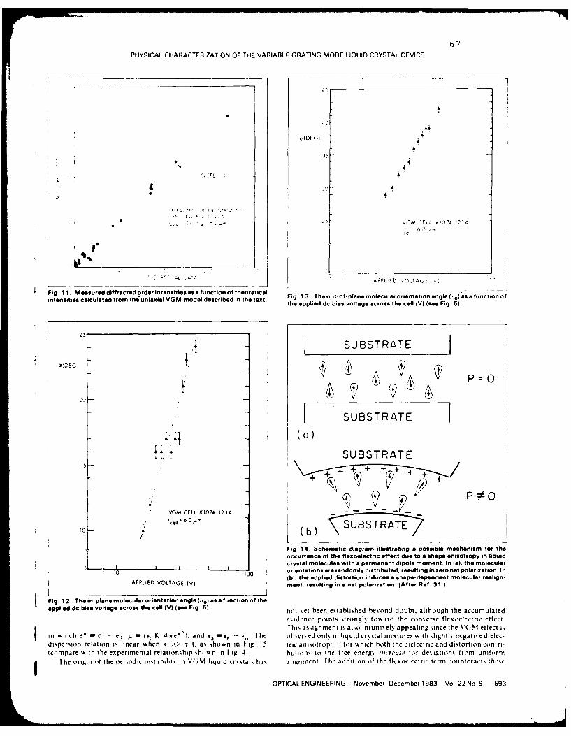
67PHYSICAL CHARACTERIZATION OF THE VARIABLE GRATING MODE LIQUID CRYSTAL DEVICE
ilPE: 1
* ~ -P e - ~GM e K r'4 1,34
e6 0
a
APPI ED VOLTAyE
I Fig. 11. Measured diffracted order intensities as a function of theoretical - ____________________
intensities calculated from the uniaxial VGM model described in the text. Fig. 13. The out-of-plane molecular orientation angle In0)l as a function ofthe applied dc bis voltage across the cell (VI lace Fig. 5).
25
SUBSTRATE
20 Po
SUBSTRATE
SUBSTRATE15
I . "'
GMCELL X1074 -)2,)AP
10 () SUBSTRATE
1, Fig. 1 4 Schematic diagram illustrating a possible mechanism for theoccurrence of the flexoeilectric effect due to a shape anisotropy in liquid
I II crystal molecules with a permanent dipole moment. In (a). the molecular10! orientations are randomly distributed, resulting in zero net polarization. In
lb), the applied distortion induces a shape-dependent molecular realign-APPLIED VOLTAGE IV) ment. resulting in a net polarization. lAtter Ref. 31.)
Fig 12 The in- plane molecular orientation angle(.,) sa function of theappled c bas oltae aros th cel (V Isse ig,5),not sect been established beyond douht. although the accumulated
esidence points strongls toward the conserse flexoelectric effect
in whch e - e e*2rhis assignment is also i ntuitisely appealing since the 'SGM effect isin hih - e , AA ~ - led K 4 1e I. andt.-t -#, The oIbsersed onl% in liquid crystal mixtures wrlih slightk ncgatixe dielec-
dispersion relation is linear when k >>' r t, as shown in Hig 15 Inc arisotrop' for wshich both the dielectric and distortion Contri-(compare with the experimental relationship show~n in Fig 41 hutiiins to the free energx irnreasi' for desialions from uniformg The origin o! the periodic instahilits in VGM liquid crystals has alignment The addition of the flexoelectric term counteracts these
OPTICAL ENGINEERING November December 1983 Vol 22 No 6 693

68TANGUAY. WU., CHAVEL. STRAND, SAWCHUK. SOFFER
onlyi one possible means of achieving parallel intensits -tl-pilt ion- .- -encoding. The processing potential of the intensit%-to-position aigs)-
%4 .. r - rtthm should pros ide more than adequate inducement to intensit'the search for alternative implementations
5. ACKNOWLEDGMENTSThe authors gratelulhN acknowledge the contributions of 1) BoswsellA. M. Lickner. and J. 1). Margerumi Hughes Research L-ihoratorics).and K. Sherman and G. Edwards (Unis ersit% of Southern Cafiloy nia)
% This research w.as supported b , the U.S Air Force Ofltice of S cicntit ic____________________________Research, Electronics and Solid State Sciences Div.ision. under grant
AFOSR-8I14)82 at the Universit% of Southern California and contractF4962(" I -C4X)l6 at Hughes Research Laboratories.
-, N'~ e~'56. REFERENCES
Fig. 16. Resultant theoretical dispersion relation for liquid crystal param-. R %i Johnson. 1) 1. Hecht, R A. Sprague. L. N Flores. I) 1.Meneters corresponding to HRL 2N40Ophentyl benzoate mixture [see Eq. 171]. meti, and 'A D) Turner. Opt. Eng. 22(f)., 665 (19831subject to the assumption that K, = K2 = K. 2. D L.. Pape and L. J Hornbeck, Opt Eng. 226b. 675 (191l
3 U. Efron. P.O. Braact, M J. Little. R. N. Schiartz. and J1 (rinheriz.Opt. Eng. 22)6). 682 1993).
4 C. Warde and J. Thackara. Opt. Eng. 22t6). 695 1903,effects, producing a free-energy minimum at nonzero distortion 5. D. Casasent. Proc. IEEE 65. 143)1977).angles. Furthermore, this model predicts a static periodic perturba- 6. S. [ipson. *Recyiciable Incoherent-to-Coherent Image Cons riers" in
tion. no h'.drodvnamic or elect roh d rodvnamic effects are observed Adane in9 Holograpsht. \ Farhat. Ed.. Marcel Dekk~er. N"s i orb.in our test cells,.' G. Knight.1 ntertact: LDeices and Memor% Materials.- in OptiaiIl)ata
The dyna mics of grating formation. reorientation, and relaxation Prcessing, S. H. Lee. Ed. Springer- Verlag. Heidelberg i)9'6are subjects of ongoing experimental and theoretical investigation. 8, A. R. Tangua\. Jr.. Proc. ARO Workshop on Future Directions sir
Understanding of the basic physical principles underlying these Optical Information Processing. Texas Tech LnisersiiN. I ubhsck.Texas. 52(19810).effects is %sital to the success of efforts to improve the VGNI LCD 9) B. H. Softer. D. Bos%4ell..M. Lackner, A R. Tangua . Jr . I I
response time. Strand. and A A. Sawchuk. in Devices and Si %items (sir ()po, a/ Siena,;A number of spatial discontinuities which are similar in appear- Processing, T C. Strand and A. R. Tangua%. Jr . Eds .Proc SP1t 2 1
ance to crystallographic dislocations can be observed within the K H H SiOr . oiel-i ake.PCae. S S )uirmliquid cr~stal layer (see Fig. 7). The "dislocation" densit'. increases C Strand. and A R. Tangua%. Jr.. in 1980 lniernaiisra/'i piaiwith time as each VGM device deteriorates. and strongly depends on puting Conterente (Boiok //. Proc Sf'IE 232. 12h) 900)the manner in which the applied bias is brought from below to above I I P Chasel. A A. Sassehuk. T C Strand. A R ITangua.. Ii . anti B3 1
the threshold ofgrating formation. In some casesas theapplied 2ia Botr Op Lo n 5. .19x 9agrmXO S.lcnr.I osel..iacross an electrically activated cell is increased or decreased, the 12BI ngua , JT C. Strd.A. % MasIch acnr P) iihjsel , A k~r
dislocations propagate past each other while the grating period tjq Cr~st '13. 145(1981)decreases or increases. respectively. Dislocations with opposite orien- 13 -i R3 Jangua . Jr . submitted for publication in iOpt f etttations propagate in opposite directions until a new stable equilib- 14 A R Tanguas. Jr.. P (bhase). T C Strand. C S %k~ u. aind H i1 'soitr.,
submitted lot publication in Opt. Letirium situation is achieved. It is not yet clear whether these disloca- 15 J B Margerum. J F Jensenand A. \1 Lackner, Mo) Urssi I Qo ( rsslions represent true disclinations. for which the liquid cry,.slt director 68. Il1_(98 1is discontinuous near the defect, or whether they are in fact alterna- 16~ (Aireubel and I Wolf). App). Phss Lett 19C). 2 131 1,-tise local continuous solutions to the free-energy minimization, per- 17 .1 % oodman. lniruiduction to Fourier Opus-i. \lctojsit)iii. V"
hapsindcedby n asvetundscoeredperurbtio. Nork ( 196))hap inuce byan s yt udisoveed ertrbaion1t B H Softer. "Real- l ime lrmplemnentatir)n of Nonlinear Optical f'toccs-
A large number of research directions base been described in the ing Functiiins.Annual Technical Rcport un .AIOSR 1.49s2U- I -(foregoing paragraphs. In addition, several others are worthy of note. 006. j(19)12).First, numerous experimental measurements of the off-diagonal 19 R B Meser. Ph~s Res leit. 221).918(19691
2)) .A I Derihanski. A. G Petro\. Chr. P Khinos. and H I Ma~rkotsK,elements in the Jones matrix describing polarized light propagation Bulg. J PhN s 2. 165 t9'4).through the VGM cell have revealed a significant asv.mmetr. not 21 NIa P Bohsles and S .A Pikin. Sos Ph\,.f IP 145ili. 14501)--,predicted by the uniaxial model. The origin of this -B C 11asvmmetrN 22 Yii P. Bob~le%. V Gi Chigriniis. and S Ai Pikin. I1 de Phis 40 'iifps,
4. ('1-331 ) 1911o,effect has not yet been elucidated. Second, the thickness dependenceol 23S A Pikin. %tl). Cryst. Liq Cr~st 63, 1 Kli 14X Ithe molecular orientation angles aand 71has not been fully established. 243MPlacndJB -nnr.SitsonomtinIsiuThe solution proposedi" in Eq. (61 assumes full surface pinning at the Intern S% mrp Digest. 143)119'6)substrate boundaries, and represents the lowest order i-dependent 25. J MI Pollack and. B H Fla nner\. in Liqiuid (r i %iaii anti r,si/ Vu.,
mode. The polarization-dependent diffracted order measurements J F .iihnsiinand R E Porter. Eds . Sol 2. pp 5'~ .fluin 'Neus Yiirk i1974)
described herein do not provide clear differentiation between a uni- 26 J M Piack and .f B Ilanner\ . in I iqiiid( ri sials andti (ir,iec, I ,.iwi
form i-dependence and the lowest order mode. Third. the nature of 3 U~ Johnson and R I~ Porter. I ds .1 Si , pp 421 442, lenum Pii- '
the transient solutions to the free-energy minimization incor porating Neui York j 197)1molecular dynamic and viscositv effects has not been treated. Solu- 2' " I K N is sun'. So\ Ph\ s -Disk)II 1 1. 90)5i 19')1
of hisprolemis ey o rspose imeoptmiztio oftheVGM 28 I K % isn', Sii\ PhNs -( r~stalliigr 151. 514) IQ-0ifinoti rbe sky orsos ieotmzation2te 9. .A IDerihanski. A 6, Petros*and MA I) Mitos J3 de t'h\s 11) 2'1 1,jsi'liquid crystal device. Fourth. it is not yet clear whether a nemnatic 10) M I Barnik. 1 M Bliniis. A \ Ifrutanis. and R A, ( iniiisk.iIlliquid crystal mixture can be found that exhibits a useful VGM effect Ph~s 39. 41'199)under ac bias. Such a mixture may provide significant immunity 3) P (i de (iennes. [he Phim siv o Liquid (Ci uta/i. pp i4- lillI(s' 5
from long-term ion-poisoning effects. Finally, it should be empha- 32 nirst ad- Pres Iacru i Jdi dePI 8 31(Iizied that the variable grating mode liquid crystal effect prov ides 33 1 Prosi and P1 S f'ershan. J App). Phss 4., 29k1) l46
694 / OPTICAL ENGINEERING INovember. December 1983 , Vol 22 No 6

174 OPTICS 11'-II'ERS / Vol 9 No 5 / May 1184 69
Polarization properties of the variable-grating-modeliquid-crystal device
A. R. Tanguay, Jr., P. Chavel,* T. C. Strand, and C. S. Wu
I iage Processing Institute und DepartmenIs of Electricul Engineering and Materiuls Science. \IC-0483. tniversfy of Southern CoI;hfrnu.Los Angeles. California 90089
B. H. Soffer
Hughes Research Laborutaries. :3011 Mulibu Canyon Road. Malibu, California 90265
Received January 4. 1984: accepted February 17. 1984
The principal features of the liquid-crystal molecular orientation within the variable-grating- mode liquid-crystaldevice have been determined as a function of the applied voltage across the cell by measurement of the polarizationproperties of light diffracted by the liquid-crystal birefringent phase grating.
The variable-grating-mode (VGM) liquid-crystal de- polarized. In addition, the even diffraction orders arevice is a two-dimensional spatial light modulator that linearly polarized parallel to the domains comprisingis capable of implementing an intensity-to-spatial- the VGM grating, as shown in Fig. 2. The even-orderfrequency conversion over an input image field.' In this intensities vary continuously with the component ofprocess, the intensity variations in an input image dis- incident polarization parallel to the domains. For inputtribution are converted to local spatial-frequency polarization perpendicular to the domains, the evenvariations in a phase-grating structure within the liq- orders are found to be almost fully extinguished. Onuid-crystal layer. As a direct result of this intensity- the other hand, the odd diffraction orders are linearlyto-spatial-frequency transduction, programmable polarized with a major axis that rotates counterclock-spatial filtering of the converted image results in se- wise with essentially constant intensity at the same ratelected modifications of the input intensities. By uti- as the input polarization is rotated clockwise. Thislizing this device concept, a wide variety of optical effect is the same as that produced by a half-wave plateprocessing and computing functions have been dem- oriented at 450 to the grating wave vector, For inputonstrated, including linearity compensation and non- polarization at 450 to the wave vector, all orders arelinear function implementation, thresholding, level observed in the far-field diffraction pattern. For thisslicing, binary logic (AND, OR, NOR. etc.), full binary situation, an analyzer placed on the output side of theaddition, and matrix addressing operations.' - :' The VGM device can be rotated to extinguish the even or-operation of this photoactivated device was described ders (when oriented parallel to the grating wave vector)in detail previously.'
An important area of research on the VGNM liquid-crvstal device is concerned with a fundamental under- OPTICAL FLATS --
standing of the origin of the variable-grating effect, if <A -
which a thin laver of certain netnatic liquid-crystal -C- .-mixtures | sandwiched between transparent conduictivecoatings (Fig. 1) is observed to exhibit a periodic re- VGM LIOU, "
fractive-index anisotropy when a dc bias voltage above CT .. i /
a threshold value is applied between the electrodes.This index modulation results in the formation of a bi-refringent phase grating characterized by a fundamentalspat ial frequency that depends on the magnitude of thevoltage across the liquid-crystal layer. The orientation ,of the grating is such that the grating wave vector is
perpendicular to the direction ofi unperturbed align TO R,
nmeri. which is homogeneous and induced by nii idirec- COUNTI Tf L -T :,V. -
tionlal rubbing or ion-beam milling. Fig'. I. GV(M liquid cr\st;tl te.t "e inetry .hw nl' the 'air
The polarization behavio r of light diffracted from tis tes .Iii o,)ur(hlimIte. . ti- reterred i) in the text a, wella' l- hehirefringent phase grating is quitt strikin . For all ili-euler 'r i t:'i inllt" cid eL Ilhi iill itri
linear input piclrization angles. the even aid odd dil kinl/ed in ihe' pLiied I1ht t dif'raciion efficienc\ uId ih,-firaction orders arc tuund to lie essetiillY linearlv h ii 'i norop -xperiebit.
111 ,6 9 -0 2 .I'" I).; pi.,il s-, o %l ,m .A l,t-r ,.i

Nla\ 1984 \i)l .N, 5 1P''l( "; I.,I7ERS 175
P,, o,-,FAcTED where A = 2p is the tundamental l)west-order) gratingwavelength.
The polarization transfer matrix can be calculated bv2 3 4 considering the uniaxial liquid-crystaL molecules at a
given spatial coordinate x to be Characterized hy a twist1 2 3 4 angle (r in the plane of the grating, followed by a tilt
VOM DOMAIN * angle q out of the plane of the grating. The Jones ma-ORIENTATION t-1
I 2 3 4 trix-1 for this case can he determined by appropriaterotations of the index ellipsoid, which Yield
1 23 [i-sin- o( I sin oo I o
Fig. 2. The polarization behavior of VIGM diffracted orders. [sin o cos o ( I - (,J,:) I - cos 2 oi - : 'The left-hand column indicates the input polarization asso-ciated with each row of output polarizations. The inset shows wherethe direction of VGM-domain orientation. t [(sin il + COS i' -1
or the odd orders (when oriented at -45' to the grating in which t is the liquid-crystal layer thickness. t,, is thewave vector). Above the voltage threshold for grating ordinary refractive index. n,. is the extraordinary re-formation, the intensities of the diffracted orders in- fractive index, and X is the wavelength of the readoutcrease dramatically as a function of increasing applied illumination employed. A uniform phase factor in ex-voltage (increasing spatial frequency) and asymptoti- pression 130 has been suppressed. The anvle.- (, and I?callv saturate. are assumed to he periodic functions of x and inde-
Observations of the VGM structure in the polarizing pendent of % and z: since the index ellipsoid will inmicroscope provide correlating evidence for the dif- general have its principal axes skewed relative to thefraction phenomena described above. For input po- original coordinate system, the polarization transferlarization perpendicular to the grating wave vector, the matrix is not diagonal.periodic modulation is observed through a parallel an- Measurement of the intensities in each diffractionalyzer to have a principal grating period p. which cor- order for a minimum set of' polarizer-analyzer orien-responds to the measured diffraction angles of the even tations uniquely determine the values of 1.4' I -. Iorders. For input polarization parallel to the grating I(',, 12, and ID, J. 'These experimentally derived value.-wave vector, the periodic modulation is observed can then be compared with the theoretically calculatedthrough a perpendicular analyzer to have a period 2p, coefficients of expression (:) lutilizing the harmonicwhich corresponds to the measured diffraction angles expansion of Eq. 12)1 for different possible assumptionsof all orders. Other input polarization orientations concerning the spatial distribution of the orientatio)nproduce apparent superposition of the p and 2p grat- angles o and qj. Simple harmonic variation ofthe out -ings, in agreement with the diffraction experiment re- of-plane angle q produces a simple phase grating thtsuits. These experiments are performed with the focus yields the polarization behavior (f t he even dilfractedset at the upper surface of the liquid-crystal layer. The orders, while similar variation of t he in-plane anhe. ,,grating contrast can be altered, and in some cases re- produces a birefringent phase grating that yields theversed, by adjusting the focal plane to lie within or below polarization behavior of the odd diffracted orders. 'liiithe liquid-crystal layer.
In the thin-grating approximation, the polarizationproperties of light diffracted by the liquid-crystal hi-refringent phase grating can be summarized by meansof a transfer matrix that connects the output polariza-tion at the rear surface of the liquid-crystal layer withthe input polarization at the front surface of the liq-uid-crystal layer. On the basis of the experimentalobservations, this matrix must be of the form
[Ao +A Ix; p) B(x; 2p) ] :[C(x;2p) Do+ID(x p)] (1) •
in which the notation A(x: p) indicates that the complex,.amplitude A varies in the x direction with periodic •repetition distance p. Fourier expansion of the transfermatrix yields the complex amplitudes A., B,, (', andD.. which completely specify the contributions of eachcomponent of the input polarization to the observedpolarization of the nth diffracted order: Fig, 1. Measured diffracted-()rder int(.nsiitt- t,,r i m-. ,,I
[A B)i A- , [ J ]p(larizer analyzer orientati)n., ;is a tunctn ,f h,rt I
Cn expnj2 rx fl c.1 (2) intensities calculated rm the uniaxial (;% n hd l (hr ,jin he text.

iT
176 )PTI(S LE'1IERS Vol. 9. No. 5 M,v 1984
dependence of the angles o and r ,m the spatial coor-dinate x has been predicted by direct minimization Ithe free energy in a similar nematic liquid-crv' lsystem."
+ The fitting procedure described above permit. theextraction of the maximum orientational excursionangles Itxtl, ' and q,,xi ,1i as functions of the appliedbias voltage above the threshold for grating formation.as shown in Fig. 4 V )] and in Fig. 5 o, ... XVf. Ineach case, it is observed that the maximum excursionangles both in and out of the plane of the grating seemto increase as the logarithm of the applied voltage. Itshould be noted that the assumption of pinned
boundary conditions with a resultant sinusoidal : de-pendence' results in an equivalently good fit. with al-
Fig. 4. The out-of-plane molecular orientation angle. tered values oft he peak orientational angles in the layeras a function of the applied dc bias voltage across the cell. center. Within experimental error, the fitting tech-V. nique described above cannot he used to discriminate
among possible z-axis variations.2, Careful experimental measurements of the off-di-
agonal elements in the -Jones matrix describing polar-ized light propagation through the VGM cell have re-vealed a statistically significant asymmetry not pre-dicted by the uniaxial model. The origin of this "asymmetry effect is under continuing investigation.
In conclusion, we have utilized the polarizationproperties of the diffracted orders from a liquid-crystalbirefringent phase grating to describe the principalfeatures of the spatial distribution of the molecularorientation within the liquid-crystal layer.
The authors gratefully acknowledge the contributionsof D. Boswell. A. M. Lackner. and J. D. Margerum
1 E K -' 'A" A dHughes Research Laboratories) and of A. A. Sawchuk(I .University of Southern California). This research wa.,supported by the U.S. Air Force Office of ScientificResearch. Electronics and Solid State Sciences Division.
_under grants AFOSR-81-0082 and AFOSR-83-01",5 atf,, the University of Southern California and contract
F49620-81-C-0086 at Hughes Research Laboratories.Fig. 5. The in-plane molecular orientation angle. o,, as * Permanent address. Institut d'Optique. 1 niversitIa function of the applied dc bias voltage across the cell, V. de Paris-Sud. BP 43. 91406 Orsav Cedex. France.
s Present address, IBM Corporation, 5600 Cottlespatial dependence can he represented by Road, San Jose, California 95193.
'= (m, co \ q= :m, sin 2 (.rV- • (4) References
The spatial distribution in the x direction of the ends 1. 13. H. Softer. J. I). Margerum. A. M. Lackner. I). lo'heil.ot the liquid-crystal molecules kat a given z coordinate A. R. Tanguav, -Jr.. T. '. Strand. A. A. Sawchuk. and '.as described by Eqs. (4) is cvcloidal in nature. Chavel. Mol. Cryst. Liq. Cryst. 70, 145- 161 (19S1 1.
An example of such a comparison between theory and 2. P. Chavel. A. A. sawchuk, T. C. Strand. A. H. Tan,ia\. -Jr.experiment for all five measurable diffracted orders is and B. H. Softer. Opt. Let 5,98 -l4o 00 19.0.
I shown in Fig. 3. In this experiment, the V;GM liquid :2. 1. H. Sfffer. I). Boswell. A. M. Lackner. '. ('havel..A. A.crystal utilized was a phenvl benzoate mixture (Hughes Sawchuk. T. C. St rand. and A. H. Tangutay..Ir.. Pr,,,., ,2N401 J, the cell thickness was 6.0 mm, ant the applied Photo-Opt. Instrum. Eng. 232, 12S 1 9, HS.voltagew,3the c t o wai the dm, sn n tis 4. B. H. Softer. 1). Boswell, A. M. lackner. A. H. Tangua,-. Jr..
was :2 V d. To obtain the data shown in this T. C. ,Strand. and A. A. Sa%chuk. Pr,,. Soc. ,, to ()t[I.figure. oma and 17.M, have been utilized as the only Instrum. Eng. 21-, 81 7 9adjustable parameters. The assumed simple harmonic 5. H. C. Jones. .J. Opt. Soc. .An. 31, . 1,1,0 9.1 ).
spatial dependence of the angles o and r is justified by 6. Yu. 1). B bylev and S. A, 'ikin. ,v. l'h\- .1.l"' 15.the quality of fit evident in Fig. :1. In addition, such a 195 -19S 19 77.
I

72
Intensity-to-spatial frequency transformations in opticalsignal processing
A. A. Sawchuk Abstract. Intensity-to-spatial frequency transformations can be ex-T. C. Strand ploited for a variety of useful optical information processing operations.University of Southern California Resolution elements of an image are encoded with a grating structureImage Processing Institute whose spatial frequency and/or orientation is a function of the localDepartment of Electrical Engineering image intensity. Assuming that certain sampling requirements are met.Los Angeles. California 90089 each intensity level is assigned to a different point in Fourier space.
Various schemes of spatial filtering can then be used to alter the relativeB. H. Soffer intensity levels. The procedure can be used for nonlinear analog pointHughes Research Laboratories transformations and for numerical processing using binary or residue3011 Malibu Canyon Road arithmetic. Theta modulation and frequency modulation are specialMalibu, California 90265 cases of the technique. Off-line methods for implementing intensity-to-
spatial frequency transformations include halftoning and grating tech.niques; real-time methods include new electro-optical systems such asthe variable-grating-mode (VGM) liquid crystal devices. Details of thesedevices and experimental results are presented.
1. INTRODUCTION certain sampling requirements are met, each intensity leel in the in
In recent years, there has been great interest in expanding the range put is assigned to different points in the Fourier domain: all point,
of operations that can be performed by optical information pro- with the same intensity in the image are assigned to the sarne point
cesing systems. Linear operations such as correlation, convolu- in Fourier space (assuming space-imariant operation is desiredi. -\
tion, and Fourier spatial filtering can be performed easily because purely absorbing spatial filter placed in the Fourier plane can then
ot the inherent linear nature of the system. 1 Three major classes of alter the relative intensity levels in an arbitrary way.
techniques for nonlinear processing involving both analog and Figure 1 illustrates the basic principle by an optical lesel-,slice c\-
discrete-level signals have been studied, and various electro-optical ample. The quantity S in Fig. I is used as a generalied patial ire-
input devices have been developed that allow real-time quency coordinate. A device is used to convert the local input in
operation. -' . The first class of techniques utilizes special halftone tensity 1uN to spatial frequency S in Fig. I(a). Figure Il(b sho,\. a
screens and an optical threshold device to convert continuous op- Fourier plane filter that selectively alters different componCnt, a- a
tical signals into sampled pulse-width modulated signals. Selective ttiictioin of S. Figure I(c) shos the ocrall 1I1 ,.rstl, _ 1 Ispatial filtering of the pulse-width modulated signal produces a characteristic found by graphically tracing through the tvko
variety of point nonlinear mappings. The second class of tech- characteristics of Fig. Il(a) and l(b).
niques uses real-time input devices having an inherent nonlinear Figure 2 sho%,s several examples of inlensit\ -to-patial irckpini \
input-output characteristic function. The choice of operating point iappings. In the most general case of tntcn'ic-.i--,pqiitlI lrtqtic\
on the device may provide the desired nonlinearity, or the device cotiersion, 1,, is mapped to an arbitrary cur\c S ill I li trCqiclt-c
may be combined in a system %%filh threshold devices, plane, as sho\\n in Fig. 2(a). locations along till, cur call can e
In this paper, we concentrate on the third class of nonlinear pro- specified in polar coordinates as ((.to). A special ca,. ho.%ii in I iu0
cessing techniques. These techniques use intensity-to-spatial fre- 2(b), is called theta WII modulation. In 0 modulation s, \arlcs alone
quency transformations in a general sense to achieve both analog all arc of constant radius L). Figure 2(c) sho\%s th- special ca,c of
and numerical processing. Devices for real-time implementation frequenc. modulation, corresponding to paths alon a line at ()Ii
such as the variable-grating mode (VGM) liquid crystal light valve lal angle 0.
are described. Intensity-to-spatial frequency conersion systems maT, he caslkprogrammed to change the functional nonlinearity by placing diV.
2. PROCESSING TECHNIQUES ferent spatial frequency filters in the Fourier plane. This program-inability i nipratahatg fsc ~tns
The basic idea of intensity-to-spatial frequency conversion is to en-code resolution elements (,- regions of an image with a gratingmodulation in which the spatial frequency and/or orientation of 3. SAMPiING CONSIDERATIONSthe grating is a function of the local image intensity. Assuming that In all the intensity-to-spatial frequency transfornations Iio\kl in
l'h, manu,,rpe i- ,uihrtitlied %iih 'hc underratiiw ihav he S (,-crm nt is Fig. 2, there is a fundamental relationship bet\een t tit i nu iber il
auihori/cd it repr,,tic m ud di'urhll reprint, hir gocronicntal purpur-C intensity level to be dislinguihed, the spatial-freqetc\ hand% Idli
SPIE Vol 373 Transformations in OprtcalSignal Processing 79871 69

73
SA IOUT AV 8e
-' -B
(a) IN(b)
(a) (b)
IOUIN V
B \\1
-S (c)U
Fig. 1. Intensity-to-spatial frequency conversion for nonlinear pro- U
cessing. (a) A device is used to convert input intensity into a varyingspatial frequency S. (b) A Fourier plane filter selectively attenuates ( Cthe spatial frequency component S. (c) The IOUT vs. INcharacteristic of the overall filtering system can be foundgraphically by tracing through the two characteristics of (a) and (b). Fig. 2. Intensity-to-spatial frequency modulation: (a) general case.
(b) theta modulation, (c) frequency modulation.
of the input function 11N, and the spatial frequency required for themodulated grating. A grating with a given fundamental frequency and we have
(L,O) in polar coordinates, corresponding to a specific input inten-sity, produces a diffraction order at ( ,) surrounded by a spectral -' = QO • (6)
island whose dimension is roughly equal to the bandwidth B of theinput. If N distinct intensity levels are to be uniquely processed by The input spectrum has width B; to place N of them in the Fourierthe system, the curve S must be chosen so that N object spectra can domain without overlap we must havebe placed along it without overlap, as shown in Fig. 2. With 0modulation and the modulated input assumed a real function, Q is NB !5 AQ = Q0 C)a constant (l), and the curve S is restricted to an arc of 7r radiansbecause of conjugate symmetry of the transform. If the number ofintensity levels N is large, we can assume that the angular width ,0 orof the object spectrum is Q) z NB. )60 = B l e . ( ) Because the band, idth B is equal to twice the highest spatial fre-If N distinct levels are needed, then we must satisfy the condition quency in the input, Eqs. (3) and (8) provide the relationship be-
twAeen the required sampling frequency Q, and the highest inputNB spatial frequency. If N is large, the %ery high spatial frequency
N60 = NB 7rx (2)
o - gratings r,-quired may be the limiting factor. Fortunately, the op-tical system does not need to image these gratings because onl, the
or modulation of the grating is important. The second part of thesystem is a spatial filtering of the spectrum in the neighborhood of
N0 = NB (3) a'single fundamental diffraction order. It is this limited spectrumi " that determines the required band idth, or resolution, of the op-
tical systemFor frequency modulation, the useful modulation range is
limited because the grating generally produces multiple diffraction 4. IMPLEMENTATIONorders. If the lowest fundamental grating frequency is Q0 and itsfirst significant harmonic is Q, the usable frequency modulation Of the intensity-to-spatial frequenc conersion techniques de-
range AQ is scribed, 0 modulation %as the first to be discussed anddemonstrated. 4 The actual implementation of the spatial frequen
AQ = Q - O" (4) cy encoding in both 0 modulation and frequency modulation stillmust be considered. One solution to the t) modulation problem is touse special halftone screens.' The screen profile combined Aith a
If we assume there are no missing orders in the grating spectrum, thresholding copy step produces halftone dots shose edges areIhen oriented as a function of the original input intensity.
le Hi nodulation inelhod i, parliiilarls vcll sited to pro e-1.lC
Q i 2 0) 2 Ql l ,t h lft i e l i g h t b e c a u s e I i " n -c c i a a t s a n i i i i o e lit t i o t i s , l it c
70 / SPIE Vol 373 rensformations in Optical Signal Processing t1981)

74
.cpataleId 11tati IhOse III a pure lrequenes titidultial~ schIente.I!dILbiia I LI% sed lialtiotic 'I modulation lechiqu-Iles tO aChiese APPLIED -d
rs~i.I~Ii~itU t a mtonochromnatic mnatte. A Ronchi rulinv (onre- VOLTAGE .
Jilicinlial constant period _,ratini) of Io%% contrast is used illn-"Il i 'l 0111t111,i01iN t0iile Input t0 scqtientiall% xp s a highil
toiai li. For eachi e\posure there is, a different aniular orien-atin I !he Ronciti ruling and a different exposure tite Assume 'AIG
i he tiotneni in iiitertmediate expotsure ltle. For loss transinit ________- LOT
1'altec area, o tlie Input, the light passing through tile sand\%ish ot LIG.T
IIputI lraitsparcilc and Ronchi ruling %illI be too %%eak to expose GLASS
lie 'tl: conras tilni. F or ighI tratimtance areas of' tile input, PLATES-
ic titert hand. light passing through tile ,andich %kill Comn-ODCTVc..c\pose thle filmn. [or a certain narros range ot' input ITO COATII"OT'
ratoli lace'detrmiedb\ thle Ronciti ruling contrast, the livhipa-~ing I hrOU'U'l Tile lad~ li ilipresses a local nmdulated arating LOQUID CRYSTAL _7PHOTOCONDUCTIVE COATING;riittire kitt tile hihL cOtitrast film. B\ changing thle e~xposure lime *-~~OVER THE CONDUCTIVE
a.Is otal tig t he screen betis ecu exposures, different ltoel-slicedITCOINCrolits It (Ilie Inputit are encoded as directional information on theii :onirai tilit. The resultant transparency is then~ placed in a Fig. 3. Schematic diagram of the VGM device construction. Cur-
,paitiall\ :olherent optical spatial filtering systemn and illuminated rent devices are read out in transmission at a wavelength at whichtilt collitmated lwigh frotm a \%[lute light point source. In the spatial the photocondluctor is insensitive. ITO (indium tin oxide) is a
treqticlic\ plane. lesel dlice information recorded for different transparent conducting electrode material.
ratnge, ot Iiput img nest ausappears as lines of diffrac-11o1l IpOrS orienited at different angles. This pattern of' spots canl beItioili ted h\ an aingular arras o0' color filters. After inverseranitorittlug. the desamnpled coittittuouN-space image has s arious 600 1 1 1
c:olor, assoctated %iill different bands of' gray levels. The 21A £ 2N40 CELL A;sseiidlcuulored iniage resultitiL from this method can be formed. 0 2N40 CELL B,it icr itl parallel as described, or as a sequeWnce ot' reconstruct ions 0 2N42 CELL CSrliti a set It spectrall\ narross band light sources. 211,42 8*2N I CELL E
Lee has recently described a system that can achiese the general * 2N25 CELL Fmodulation of' Fig. 2(a) or the special cases of 0 or frequency 50 -X 2N43 CELL Gmodulation 'A scanning interferometric systemn is used to encode 21 EC ~each spatial resolution element of an image as a small grating seg-ment whose frequency and orientation can be changed with input ( IIIEC
intensity lesels. The system does not currently operate at television 4rates (30 frames per second or faster) but can utilize the two- C
dimensional nature 0of the Fourier plane better than either the 0 or Wi 400- 2 N 43frequency modulation techniques. Zj
2N255. VARIABLE-GRATING MODE (VGM) DEVICES wFast implementation of intensity-to-spatial frequency transforma- W
tions by frequency modulation has recently become possible with 0 300-the deselopment of sariable-grating mode ( VGM%) liquid crystal c(LUC) electro-optical desices."iII The VGWeiei hw
scheaticllyin Fig. 3. It consists of a thin (thickness < 12 ;Am)
nemnatic LC layer sandwiched with a photoconductor between twotransparent ITO (indium tin oxide) electrodes. If a dc voltage is ap- >20plied across ihe liquid crystal cell, a periodic phase grating structureis produced in the LC material. As the voltage is varied, the periodof the grating changtes as shown in Fig. 4. The fundamental VGM 244spatial frequency is a roughly linear function of applied v oltage forN4seseral different LC mixtures. Typically the spatial frequency%aries from 200 to 600 line pairs mm. Figure 5 shows the LUmaterial in a cell as viewsed through a polarizing microscope. 0 20 40 60 80 (00 120
The %oltave across the I U cell canl be localllk controlled by pro- APPLIED VOLTAGE, VOLTS DCct ITIQ art Input IntaCe tt (Ilie VGNI des ice at a ss as letugtlt at ss hicliI
the pliotoconductor is crisitise. [Hills file V(\1 des ice series as an Fig. 4. VOM spatial frequency as a function of applied voltageInitensits -toispat tal trequencN cons crier. The photoconductinglaser of the cell is designed to actepi n1it t lie Htas '.oltage withtio illuminnation; tha: portion of the % ltlave falling2 across thie [C isbelos the actisation threshold oh tie %\IM effect \\ lien light falls tate been tabricated b\, Hlughes Researchl I aboraiiirtes. old ecxcioin the photoconductoir, its Inipedanice drops. I hereb% sitnching the sit C Miodelinig anid cx pertmntnal v. or k is untderts a\ I ITIh~ isiihtave from the photocotiduclor onto the [U mtaterial a nd ac- cliaractertie the \(M~ nmechianisnm. I pical des Ices liii a /t
ntitig the %U\1I effect. The high lateral Imipedatice of tie thin phiotliconductor. .( onistriictntiI det~ails of the (,Ni &\es Icl.td~ .1
film lasers allo%%s 5 er% little spreading of the plhtoio0induiCed con1- ulsusofl I ( rlil sics are git Ci ii set erai relereticesducts nt% pattern or of the associated I.U electro-optnc effect. As aresult, the light actuation has inherent]\ hi ' h resolution, arid the 6. V(,M IMPLEMEKNTATION OF A LEVFI.-SLIILdeuice accepts photographic qualit% imiages. Seseral 's(A k\ldsices \tt C1pertiCIental t11iCipeiitttattiin Il A lesC LI11,iC Itilic11TuIt ilEll J
SPIE Vol 373 Transformations in OptIcal SIgnal Processin t981i 71

757
CM7
_0 -0 0 0 0 0 0 0 0
Fig =.VMvee hog oaiigmcocp safnto fapidvlae
Ait*sno e lsrt leseo ddfrcin )d i - :
W ~ ~ A 7i 5G% VGM vAewed inhroughnc polarizin microscop as a fucto ofaplidvotae
iL. T -- I are due to reflections tin the external apparatus.
7. J(A IPIINII-N'IAJIN M011 (il~~ I ((,I(- 5A'. It I, is Isblc To use lie NN (ANIc 'e
The. kesii sILI ~ ilser~iilot lies! notm
A . rpresenItid ats i sittiple hiiiai\ niinea I \
characteristics ii tOUT halil,: c tiicu I'cll],:
Fig. 6. Experimental setup used to perform the level slice ex- input InI these tficures is A.isIuIIIcd TI he '11Cliplperiments. The spatial filter is a variable annular aperture. The [\o iniput lo'ic ci i' I i' \M ), I isla:p!
seiier ..- \I) ,uI)Iu ()R mit ii'uliiie.ii I'ITCs,i i'do1
isk lC\el slice tW11,1ii011, I hiese tuuriii j: 5
i
\(A Li es ice lias been perfornmed. Tite csperinietitl arrancpenientis iii mdtlator or h\ opiicil prisesir stin,Tm 'i-if,
.hiNn iiIt I-ic. 6. A\ contittuous toile input picture is Illiutminatedl h\ niitiieanities, 11id CMI he Hiuse t iplie'lii 1 r,III ire latitp source atnd iniauaed onto the photoeonductor surface of I. Fiirtieritiore. it lhe ilksteNt i tisleeh.tk b ee
I (Gl de% ice tht initiall% eshibit, a Uniform phtase g'rating sirec- floduced. sequientii or L1ichiutic -oi cnilo 11 ! pltic'
,ture due to a dc bias soltage. The itratinge period is locall\ [ lie \rCjNI deiceIC 11 \ell siedIC 11) i-iipleri1iiiiti heseI 1iiiiodiilaicd h% the input Picture intensits, and this tnodnilaiion is lirtearies. \\,I', lie \ ("1 arippo-u: tiit is c h
ttapped into a positon along at line in the spatial filter platne. A red nI I0 lOut IC plirie I liter %k hose ! rXIIsIII:iie 11,C ITitiP
tiller ensures that ortlv the readout laser beam) enters lie cohiereti diiieiisioii esseitialls 'I Plo1 ot he desitedlrrei 111 i1s,11 I u'1topiical processor. Sectors of small circular annult of sar~ itg radii biirair itotiuttarities ire eaiil I-Julcd 1iiid chiMIieed I 'T1 'are used to pass certain spatial frequencv banids. Thlis, allosis onIN opertionts lie situaiwo is quite staciinsi.xii~c t heprescribed input intetnsity ranges to appear tit tile output. Circular 1itottlitic: Tire' 111iXsCI~ie IN Iii hoerI11ena , Iioire iittiti.
rather thain traight slits are used to capture the k~eal, light shiich 1ic\ cani he Ittplemiinted ss I simple '1 li petures. ic. 0i OTI
in small part is diffracted into circular arcs because of the grating Iatti iii1111 n: it % 31C. i \ IC0 I C~ Of Ti e \i ie ( 1\1 I ecl:i1ii c 111, I I k Hi
Imperfections (see Fig. 4). Figure 7 sltosss both (fie input anid les el- it espC il l elii ted I or locl. pi Cess tc 1, t11 iei hc;p i ipit
sliced output pictures. Figure 7(a) shos a positise print of the Output titc pis uc~lls\ set"iiaie betitu I lie Itpui be"oii riodtiikitcs
orga img hog .hes~e si appears on the imaging phtoimducior, octtiticniks lie ititc is reaid oi ut it a weoiid
sreen. A negatise of he original was used in the experimntt. beatti I its1 sepaiiiioii 0t itipir itid oiiip-iii pios ides " tiehFigure 70b) shows l o\& intensiv. lesel slice correspondittg to at possibilis of tesiotirie ouitut lesC1 10s t1oXeII ii I s .iliiesCI cici i
VGNI spatial frequecncs of' IMX line pairs. mm sw.ith approximiatels i'lie Input letCI Ils ii1,io eic I ot tcci. IhisI I ealt ie is cs'cri.1 iiljS iro fractional bandwidth. H-ere fractional bandwsidth is defined as i'lie pr *h ci iouti ,I reliable b i \sIcnii i(tat is iiiiiic !0 ise"
shelit w idth in the Fourier plane dii ided b,, distance betwseen first mid~ s\sicrii, cetiot s iiiti) lirs lcb I len routuc loct clenwIcIit
and second diffraction orders. Figures, 7(c) through 7(t) are a Ne- such lesecl testorutic c-ipaihI\, but oilici ciiriirs 1 tpic
quence of let el slice outputs at successively higher input intettsitN\ h0 11 scltnC1 lu1cf i11 17"is 13 essiti iMilch t a te
lel.The Fourier plane slit hating the same 1 517, fractional band- I iso tuliC a "ec I locte opcriiuiuts tuakc tluciti 1JIIWi )1
72 1 SPIE Vol 373 Transformations in OpricalSignal Processing (1981u

(c76
Fig. 7. VGM level slice results.
vGM F;.'eOUT NOT OUT AND _"s'e,,ce
0 A
1 2 IN 1 2 IN -3, -
(a) (b)Rec do u2
I BSearn
OTOR OT6 XOR q g9. Experimental arrangement for performing logical opera1 - I- -1 ions n two-dimensional binary inputs with a VGM device. Input
image arrays A and B are superimposed on the photoconductorThe device is read out in transmission at a wavelength ditterent
0 o- from teinput. Simple slit apertures are used to achieve the desiredf 2 IN 1 2 IN logic functions.
(C)~~ (d 'eries Ot espreri nients as condct,:ed to dernonit': !hi iFig 8. Logic functions as simple nonlinearities. Given an input daHCrtrrnrllot tiletiort'. Thle experinierial cliri ot 1 ig.1consisting of the sum of two binary inputs, different logical opera. used Thle toial ilitlialurrOn llttrrit\I on the phlotocoridu' !Ictof0tions can be effacted on those inputs by means of the depicted %0(\11 Je ice ssas tire sutm of the isso input intentiesic aind Ia- :i'nonlinear characteristics: (a) NOT. Mb AND. (c) OR. and (d) XOR. reisu% Thie inti illumninatton %% as pros ided h,\ .1 t lirred hi cli-
pressure Itlrrr arc lamp, thle bras illumntiton h\s ai olilltj'pi ml tpicttieittalro ptrrpiise: (,l lout,. operartion itiprii rungstert bilh sourc. rire \GMN de\ ice \Nsa' read out ini'.itrt~
ire di,,.rcte. Ad ill 01hI orI nr iall nuitiher (2 -1) of sion ursitng a HeNe laser. A filter ssaN placed tit the Ilourte: planejo 't~iisial leels arre requtired. The esistetree ii discrete itrpit select the desired difiractiont orders tor eacht loo.vi tiirtintcc'itrlies that rlite rriirrrtte treed not Irase tite esact torirts For these esperimerirs, tire inputs consisted 1rt oneC serti~ii rec:oos itl I i, I<. itt particular rlite transitionl regtotrs treed rfihe nangular aperture arid one horriontal aperture. Wi en ilrese sNcre
jl,,Ik liirrp irresiilds. since rthe inpurt salues are presumlled riot superimiposed along ss ilt tie bias. a square nrave \kas torried us ilt,,I _ir fsiitlie rrarrsrion reL'torrs fit amt esett Tile fact liar tle forir quadrants hllt t(lhe linrensits lesels sltossru III I I. Ltl. 1111,
al I ess, les els tneed be diirrilidiplies rthat thle in-lsl itLe corresponds to (fie loick truth table shosn it hllc olieOtpiutc':,ltti'tt requiiremntt for tile ,sierrre rtrtttrtrtal. tni1ages hase irtensit lesels deteriirred b\ tlietruth tallrscae,
Tile Operations discussed abos e arc the basic combinatorial logtic ss it tile desired logic furrettiorn, Ile logic tunrcitis AM ), OR,trirretons. Hosses er. sequential logic may also be implenrented \kith XOR, and their conlpletncetfi s"sere timplernted .eqrrerrtials isappropriate feedback, i.e., imiagiing the Output plane onto the input 1it0"ll itt Fig. lit by altering orll\ tre Fourrer platte htner. lrttpertec:plane tsdtlieh can be accomplished w~ith incoherent illurminatron)t. tions sisible In tile ourIpWr plane darta arrse tront detects Intt ite cell1Ho%%eCser. skith the present WGiM trarnsmnission des tees thmere is a st rructure of rte \(MN des tee etrtplo\ ed Itt thiese e\perttrrertt. lInproblem of separating thre read and %s rte fuinctionts in a feedbacek s est gatltOrs Ol %(M NCIeste impros e~ltmirr . lititit oll Iu t t o 11't ire
sssem ine tei s~aslergts mstbe identrealarid current des ices speed, and pisel iitflortitt are in progress.stork inl tranisntission . Its adliitev teedhlack, io isplial coiitttitiral loct.. tttetitr
SPIE Vol 373 Trans formations in Optical Slional Prncpsstnq ut981 73

~~tI l C' 1iI il ne ileie A i ;! IC II W1,1 3 Ve ' IIti r lk '
comI crsii ajnd %(,',I Jc% I c'L.
8. OTH ER .APP1,1(A I 10 NS 01f- (0* 1) V I (IVSt V~al able gratino :clIl Ilak A a n ntiet If e i ItC '
Wn bnih ejeetricailk ja,! i\Ad m~d tl''.J-Iltenn'. I-lecti clkIt kil Iolale % .rati'le LCIal'T
lt~r moidiilaiiik i ranic!r Tll, nt'rl cIT :i I-;heani dceetor'. oir Ip~olal icilloiI: ' -
nialkl Inr ctrreclatot,. B\ in!rdiu:nej Aow~lra patialk %art I aMCC CL:ec:,Ia' , A! 1 ALt Cd Lr! !,1!
I Inc I I()l couIIJ he : l! id ),J l'~ iid u ,) I ,could ako crkc a prtlrarnnlahjc raiialit\A
g rat ln L!.
- - - -9. CONC1L SIONS
e haLIe delcrihed eCral Lelieral lechiqUe, oIflatlal trequenc\ tratti I o irk1 and anl elec r-r Il _ ri1
eraurv-rnnd (\I transdllcer capalei ol rval-l ntlm'vn on. \% e ha% e ho%%ifI rheorentca I k ld \eN ITlrneTm\ ha! heJet ice can he Lbe~d for implemnent , arhhrrar%\ nointer:nu ii;-cOIItn0IIO'Orte lfnateC afld call he kijed lor oniFra
n peCat on )in linart da ta arra\. An aidt % ae 't, hl \ (IIproach ip t hat ii tna\ cal il\ be pro-ramtneO bx '"tj.aI 'patial t~c-n.Oher arrpicallton, tor ;llteloh
q c o!1erion hate hibeen Jlecribed.
ACK NO~ 0 1IX DM L\ I S\\I tti'hi acknItle6d,_t !he ippol "I he No1 I 7 --
Selt Rc'earch. I-Letionic, and ma terial, pr 1):,wider Grant, \H-)SR----12 and \I GNR Sl ')12 a 1 1(1"
( 1c -~~n -(08 IT) J an 149t(l" 1 .Xt.
Rc'earch [ ahoraiorwe. \\ C alo aeknott 'ippor' ! Tllp101lSc::rCIe I Ls ndalln.11 unIder (,raott I \ I '
Ipmt Ner\ i~c F 1et:roniuc lrrn I a t '0I he ainiltor' Are eratetiji :ko N. -rtn d, 11 Ie\1 !! N K
Ia::wtla\ . I' r t , or eIr :011tr bI'11101) o '1!he te i
R 41 REN CLS
jI \\ ij~i wd I l I 'I N
I, J \IIl 1" PN p
I '11 1 tl All I
)j, 'ii I' ''< ' A P N
levlsfo a iag cnsstig f ou qadans lifl~ . ) \L. I ''i I N, k I
NOR. AND NAO XOM.ll and N\R repciey I' c.. 11j, I-ti
'4 ~ ~ ~ ~ ~ ~ ~ ~ ~ ~ ~ ~ md S1Wit V',l 07, ;rrira~n nOtiC/lOlPnPsn(9
78
'.5 References
A.A. Sawchuk and T.C. Strand, "Fourier O t cs in NonlnearS>gnal Processing," Ch 9 of An pliations of Oo, 4a Forier.-.ansform, H. Stark, ed., Academic, New York, 19 1.
A. Armand, A.A. Sawchuk, T.C. Strand, B.H. Sofer adD. Boswell, "Real-time Parallel Opt cal Analog-to-DicitalL,3nversion," Ootics Letters, vol. 5, pp. 129-131, 1980.
. P. Chavel, A.A. Sawchuk, T.C. Strand, A.R. Tanguay, Jr., andB.H. Soffer, "Optical Logic with Variable-Grating-ModeLiquid-Crystal Devices," Cotics Letters, vol. 5, pp. 398-400,1980.
4. B.H. Soffer, j.D. Margerum, A.M. Lackner, D. Boswell,A.A. Sawchuk, T.C. Strand, A.R. Tanguav, Jr., and P. C(have-,"Variable Grating Mode Liquid Cry'stal Device or Ootica:Processing and ComoutinC," Molecular Crvstals and CIauidCrystals, vol. -9, pp. 145-161, 1981.
5. A.A. SawcnuK, "Intensity-to-spatial FrequencyTransformations," Proceedinas Socoety. _°f Photo-Opt ca..nstrumentation Engineers Advanced Institute of Transformations-n Ootical Siqnal Processing, Seattle, February 1981).
6. A.A. Sawcnuk, "Recent Developments in Optical and DigitalProcessing," Proceedings Workshoo on Optical InformationP-ocessing, Centro de investigaciones en Optica, Cuernavaca,Mexico, (January 1982.
A.R. Tanguay, Jr., P. Chavel, T.C. Strand, J. Wu, andB.H. Soffer, "Physical Characterization of the Variable GratingModel Liquid Crystal Devices," SPIE Proc. Advances in Ootical.nformation Processing, vol. 388, January 1983 .
3. A.R. Tanguay, Jr., P. Chavel, T.C. Strand, C.S. Wu, andB.H. Soffer, "Polarization Properties of The Variable GratinQMod cs___ °et rs vol. 9, op. ! 4Mode Liquid Crystal Device," tcs Leers o.9..1934.
9. A.R. Tanguay, Jr., T.C. Strand, P. Chavel, A.A. SawchuK, andB.H. Soffer, "Theoretical and Experimental PoarizationProperties of the Variable Grating Mode Liq1Uid Cr-yst aStructure," presented at 1981 Annual Meeting, Optica3 Society ofAmerica, Orlando, Florida, October 1981, Journal of the Oot calSociety of America, vol. 71, p. 1630, (December 1981).
10. A.R. Tanguay, Jr., "Recent Progress in Spatial LightModulators for Coherent Optical Processing Applications," 1982Gordon Conference on Holography and Optical informationProcessing, Plymouth, New Hampshire, 1982.

79
11. A.R. Tanguay, Jr., "Polarization Properties of BirefringentPhase Gratings," presented at 1982 AnnuaL Meeting, oticalSociety of America, Tucson, Arizona, October 1982: Journal of theOotical Society of America, vol. 72, (1982).
12. A.R. Tanguay, Jr., "Spatial Light Modular-rs for Real TimeOptical Processing," Proc. ARO Workshop or Future Directions forOptical Information Processing, pp. 52-76, Lubbock, Texas, May,1980.
13. P.G. de Gennes, The Physics of Liquid Crystals ClaredonPress, Oxford, (1975).
14. Yu P. Bobylev and S.A. Pikin, "Threshold PiezoelectricInstability in a Liquid Crystal," Soy. Phys. JETP, vol. 45,pp. 195-198, (1977).
15. R.B. Meyer, Phys. Rev. Lett., vol. 22, 918, (1969).
16. P. Auborg, J.P. Huignard, N. Hareng, and R.A. Mullen, "LiquidCrystal Light Valve Using Bulk Monocrystalline Bi SiO as "hePhotoconductive Material," Appl. Opt., vol. 21, 3706-3711,(1982).
i

80
2. PROFESSIONAL PERSONNEL
The following individuals contributed to the research effort
supported by this grant during the period April 15, 1981 to June
30, 1984.
I. Alexander A. Sawchuk, Professor, Deoartment of E.ectricalEngineering, Director - Image Processing Institute, PrincipalInvestigator.
2. Timothy C. Strand, Research Assistant Professor, ImageProcessing institute, Senior Investigator.
3. Armand R. Tanguay, Jr., Associate Professor, Departments ofElectrical Engineering and Materials Science, and ImageProcessing Institute, Senior Investicator.
4. Pierre H. Chavel, Visiting Research Scientlst, ImageProcessing Institute (on leave from Institut d'Optique, Orsav,France).
5. Robert Forchheimer, Visiting Research Scientist, imageProcessing Institute (on leave from Linkoping University,Linkoping, Sweden).
6. B. Keith Jenkins, Research Assistant Professor, Department Electrical Engineering.
John Wu, Research Assistant, Ph.D. Candidate, Departmen ,.'-
Electrical Engineering.
The following individuals have received degrees from tne
University of Southern California while participating in tre
research effort:
1. B. Keith Jenkins, Ph.D., Electrical Engineer ng, Mav 952thesis title: "Optical Logic Systems: mpleoentaronw>:Architectural impi icat ions," published as SCP1110).

81
3. PUBLICATIONS
This section lists written publications resulting from AFOSR
support of this project during the period April 15, 1981 to June
30, 1984.
1. A.A. Sawchuk and T.C. Strand, "Fourier Optics in NonlinearSignal Processing," Ch. 9 of ADolications of Optical FourierTransforms, H. Stark, ed., Academic, New York, (1981T.
2. A. Armand, A.A. Sawchuk and T.C. Strand, "Nonlinear OpticalProcessing with Halftones: Accurate Predictions for Decradarionand Compensation," in preparation for Applied Optics.
3. A. Armand, A.A. Sawchuk, T.C. Strand, and B... Soffer,"Real-Time Parallel Logarithmic Filtering," Ctics Letters,vol. 7, pp. 451-453, (September 1982).
4. B.H. Sotfer, J.D. Margerum, A.M. Lackner, D. Boswell,A.A. Sawchuk, A.R. Tanguay, Jr., T.C. Strand, and P. Chavel,"Variable Grating Mode Liqui - Crystal Device for OpticalProcessing and Computing," Molecular Crvstals and LicuidCrystals, vol. 70, pp. 145-161, (1981
5. A.A. Sawchuk, "Intensity-to-Spatial FrequencyTransformations," Proceedings Society of Photo-OpticalInstrumentation Engineers Advanced Institute on Transformationsin 0 tical Signal Processing, vol. 373, pp. 69-75, (February1981
6. A.A. Sawchuk, "Recent Developments in Optical and DigitaProcessing," Kinam, vol. 5, Serie C, pp. 109-112, (1983).
7. A.R. Tanguay, Jr., C.S. Wu, P. Chavel, T.C. Strand,A.A. Sawchuk, and B.H. Soffer, "Physical Characterization of theVariable Grating Mode Liquid Crystal Device," SP1E Proc. Advanc.esin 0ptical Information Processing, vol. 388, pp. 35-95, January1983).
8. A.R. Tanguay, Jr., P. Chavel, T.C. Strand, C.S. Wu, andB.H. Soffer, "Polarization Properties ot the Variable GratiniModel Liquid Crystal Device," Optics Letters, V,)1.pp. 174-176, (May 1984).
9. P. Chavel, R. Forchheimer, B.K. Jenkins, A.A. SawcliuK, aridT.C. Strand, "Architectures for a Sequential Optical Loai,Processor," Proceedings 10th International Optical Con[utxn:jConference, IEEE Cat. No. 83CH1880-4, pp. 6-12, (April 183).

82
10. A.R.Tanguay, Jr., C.S. Wu, P. Chavel, T.C. Strand, andA.A. Sawchuk, "Physical Characterization of the Variable GratingMode Liquid Crystal Device", Optical Engineerina, Vol. 22,pp. 687-694 (November/December 1933.
11. B.K. Jenkins, A.A. Sawchuk, T.C. Strand, R. Forchheimer,andB.H. Soffer, "Sequential Optical Logic Implementation," AppliedOptics, vol. 23, pp. 3455-3464, '1 October 1984).
12. B.K. Jenkins and T.C. Strand, "Computer-Generated Hologramsfor Space-Variant interconnections in Optical Logic Systems,"SPIE Proc., vol. 437, pp. 110-113, (1983).
13. B.K. Jenkins, P. Chavel, R. Forchheimer, A.A. Sawchuk andT.C. Strand," Architectural :mplications of Digital OpticalProcessors", Applied Optics, vol. 23, pp. 3465-3474, (1 October1984).
14. A.A. Sawchuk, "Digital Logic and Comouting with Cotics," SP13
Proc., vol. 456 (1984).
15. A.A. Sawchuk and T.C. Strand, "Digital Optical Computing,"Proc. IEEE, vol. 72, pp. 758-770 (1984).
16. B.K. Jenkins and A.A. Sawchuk, "Characteristics of DigitalOptical Processors," Proceedings of the IEEE GlobalTelecommunications Conference, Atlanta, Georgia (November 19841.
17. B.K. Jenkins, A.A. Sawchuk, and T.C. Strand, "Spatial LightModulator Requirements for Sequential Optical Logic," inpreparation for Applied Optics.
18. A.A. Sawchuk, "Numerical Optical Computing Techniques,"Proc. 13th Congress of the International Commission for Optics,ICO-13, pp. 6-9, (August 1984).

3 74. ORAL PRESENTATIONS
This section lists oral presentations at meetings and
conferences describing research supported by this grant durin
the period April 15, 1981 to June 30, 1984.
1. A.R. Tanguay, Jr., T.C. Strand, P. Chavel, A.A. Sawcnuk andB.H. Soffer, "Theoretical and Experimental PolarizaticonProperties of the Variable Grating Mode Liquid CrystalStructure," presented at 1981 Annual Meeting, Optical Society ofAmerica, Orlando, Florida, October 1981, Journal of the OpticalSociety of America, vol. 71, p. 1630, (December 1981).
2. A.R. Tanguay, Jr., "Recent Progress in Spatial Lign-Modulators for Coherent Optical Processing Applications," 1982Gordon Research Conference on Holography and Optical :nformation.Processing, Plymouth, New Hampshire, (1982), (Invited Paper).
3. A.R. Tanguay, Jr., "Polarization Properties of BirefringentPhase Gratings," 1982 Gordon Research Conference on Holograpnyand Optical Information Processing, Plymouth, New Hampshire,(1982), (Invited Paper).
4. B.K. Jenkins, A.A. Sawchuk, T.C. Strand, and B.H. Soffer,"Sequential Optical Logic Implementation," presented at 1982Annual Meeting, Optical Society of America, Tucson, Arizona,October 1982; Journal of the Optical Society of America, vol. 72,p. 1721, (1982-.
5. A.R. Tanguay, Jr., "Polarization Properties of BirefringentPhase Gratings," presented at 1982 Annual Meeting, OpticalSociety of America, Tucson, Arizona, October 1982; Journal of theOptical Society of America, Vol. 72, p. 1832, (19827.
6. B.K. Jenkins and T.C. Strand, "Computer- lenerated Hologramsfor Space-Variant Interconnections in Opt_:-al Logic Systems,"Annual Meeting of. the SPIE, San Diego, Califo:zna (August 1983).
7. B.K. Jenkins, A.A. Sawchuk, T.C. Strand, "Spatial Lign*Modulator Requirements for Sequential Optics. Log.c," presente,at 1983 Annual Meeting, Optical Society of America, New Orleans,October 1983; Journal of the Optical Society )f America, Vol. 73,(1983).
8. A.A. Sawchuk and T.C. Strand, "Digital Optical ComputingTechniques", presented at 1983 Annual Meeting, Optical Society -fAmerica, New Orleans, October 1983; Journal of the OpticalSociety of America, Vol. 73, (1983).

84
9. A.A. Sawchuk, "Digital Logic and Computing with Optics,"presented at SP[E Technical Symposium, Los Angeles (January1984).
10. A.A. Sawchuk, "Numerical Optical Computing Techniques,"presented at 13th Congress of the international Ccmmission forOptics, !CO-l3, Sapporo, Japan, (August 1984).