
Holographic Optical Manipulation of Trapped Ions ... - UWSpace
70
Holographic Optical Manipulation of Trapped Ions for Quantum Simulation by Chung-You Shih A thesis presented to the University of Waterloo in fulfillment of the thesis requirement for the degree of Master of Science in Physics (Quantum Information) Waterloo, Ontario, Canada, 2019 Chung-You Shih 2019
-
Upload
khangminh22 -
Category
Documents
-
view
10 -
download
0
Transcript of Holographic Optical Manipulation of Trapped Ions ... - UWSpace

Holographic Optical Manipulation ofTrapped Ions for Quantum
Simulation
by
Chung-You Shih
A thesispresented to the University of Waterloo
in fulfillment of thethesis requirement for the degree of
Master of Sciencein
Physics (Quantum Information)
Waterloo, Ontario, Canada, 2019
© Chung-You Shih 2019

Author’s Declaration
I hereby declare that I am the sole author of this thesis. This is a true copy of the thesis,including any required final revisions, as accepted by my examiners.
I understand that my thesis may be made electronically available to the public.
ii
Abstract
Trapped ion is one of the leading platforms for quantum simulation experiment due to itslong coherence time and high fidelity state initialization, detection, and manipulation. Toindividually address ions at a single-ion level, it requires sophisticated optical engineering.In the thesis, we present a novel single qubit addressing system that is immune to imper-fections of optical imaging and can scale to different size of the system. The technique isbased on digital light processing with a commercially available digital micro-mirror device(DMD).
A DMD is a 2D array that consists of tiny micro-mirrors that can be individually ma-nipulated. It is commonly used in movie projectors to modulate the intensity of the lightto create the desired image. However, using this technology to ions will require more so-phisticated controls over optical wavefronts of the laser beams, for example, the necessityto manipulate the optical phase. It can be achieved by using the DMD as a programmablehologram, which can then be used to characterize and compensate for any imaging im-perfections as well. We developed a new iterative Fourier transform algorithm (IFTA) forcalculating the holograms. In the simulation, our algorithm shows more than one orderof magnitude improvement in accuracy comparing to previously proposed algorithms. Weexperimentally demonstrated this holographic beam shaping technique with the opticalaberration being compensated. The laser we used in the experiment is in the ultraviolet(UV) regime that is close to the optical transition used for manipulating 171Yb+ qubits.The short wavelength makes it more susceptible to environmental disturbance.
Also, we proposed and experimentally demonstrated a new scheme that enables holo-graphic controls over lights with multiple laser frequencies simultaneously by combing theDMD with an acousto-optical modulator (AOM). The AOM splits the light and illuminatesdifferent zones of the DMD. Each zone has its own hologram forming one frequency chan-nel for addressing. This opens the possibility to engineer more complex Hamiltonian forquantum simulation. For example, we can engineer arbitrary spin-spin interaction graphsby applying the Mølmer-Sørensen scheme on this new setup.
iii
Acknowledgements
First I want to thank my advisor, Dr. Kazi Rajibul Islam, for offering this wonderful andunique opportunity to be one of his first graduate students participating in the research inthe Quantum Information with Trapped Ions group (QITI Lab). He is an amazing advisor.It is lucky for me to have his support, and I always enjoy the time of discussing physicswith him.
I want to thank my advisory committee and thesis commitee, Dr. Thomas Jennewein,Dr. Michal Bajcsy, and Dr. Kevin Resch, for their valuable advice on my research. Itis their valuable suggestions make this works better. I also want to thank Professor Dr.Crystal Senko for her amazing lectures on trapped ions. This course is a great aid inhelping me get into this field.
I want to thank my wonderful colleagues, Nikhil, Sainath, Nikolay, Kaleb, Fereshteh,Roland in QITI Lab and Rich, Brendan, Pei Jiang, Noah, Matt from Dr. Senko’s group.group.It is an amazing experience to build the lab from scratch with them, and I always learneda lot from all our energetic discussions. I would like to thank all my friends here or inTaiwan My life as a master student will not be as happy as it is without them.
Last but not least, I would like to express my gratitude to my families, especially myparents. It is their support that makes me able to be here and pursue my dream.
iv

Dedication
This is dedicated to those I love.
v

Table of Contents
1 Introduction to trapped ion quantum simulation 1
1.1 Trapped ion qubit preparation . . . . . . . . . . . . . . . . . . . . . . . . . 2
1.2 Interaction in trapped ions system . . . . . . . . . . . . . . . . . . . . . . . 5
1.3 Thesis Outline . . . . . . . . . . . . . . . . . . . . . . . . . . . . . . . . . . 7
2 Holographic Beam Shaping for Quantum Simulation 8
2.1 Individual Addressing . . . . . . . . . . . . . . . . . . . . . . . . . . . . . . 8
2.2 Fourier Holography . . . . . . . . . . . . . . . . . . . . . . . . . . . . . . . 11
2.3 Digital Micro-Mirror Device . . . . . . . . . . . . . . . . . . . . . . . . . . 13
2.4 Off-Axis Amplitude Hologram . . . . . . . . . . . . . . . . . . . . . . . . . 16
2.5 Binarization . . . . . . . . . . . . . . . . . . . . . . . . . . . . . . . . . . . 18
2.6 Iterative Fourier Transform Algorithm . . . . . . . . . . . . . . . . . . . . 25
2.7 Chapter Summary . . . . . . . . . . . . . . . . . . . . . . . . . . . . . . . 29
3 Calibration and Use Cases 30
3.1 Aberration Phase Profile Measurement . . . . . . . . . . . . . . . . . . . . 30
3.2 Aberration Calibration with An Ion . . . . . . . . . . . . . . . . . . . . . . 34
3.3 Maximizing Diffraction Efficiency . . . . . . . . . . . . . . . . . . . . . . . 35
3.4 Use case: Linear Gradient Intensity . . . . . . . . . . . . . . . . . . . . . . 37
3.5 Chapter Summary . . . . . . . . . . . . . . . . . . . . . . . . . . . . . . . 41
vi

4 Holographic Addressing with Multiple Frequency Channels 43
4.1 Frequency Channels Preparation . . . . . . . . . . . . . . . . . . . . . . . . 45
4.2 Experiment Results . . . . . . . . . . . . . . . . . . . . . . . . . . . . . . . 48
4.3 Chapter Summary . . . . . . . . . . . . . . . . . . . . . . . . . . . . . . . 51
5 Summary and Outlook 53
References 55
APPENDICES 58
A Branching Ration of D1 and D2 Line in 171Yb+ 59
B Holographic Beam Shaping with Pulsed Laser 62
vii

Chapter 1
Introduction to trapped ion quantumsimulation
Quantum computation has the potential to fundamentally change our society, from break-ing standard encryption algorithms [18] to accelerating machine learning techniques [1].While a large-scale quantum computer is perhaps years away, moderately sized special-purpose computing machines, called quantum simulators are already useful in solvingproblems in quantum many-particle physics and quantum chemistry. Quantum simula-tors have the potential to shed light on the origin of high-temperature superconductivity,to discover new phases of matter, and to find new drug molecules.
Long coherence times[22], high fidelity qubit state initialization and detection, andprogrammable long-range interactions make trapped ions a leading platform for quantumsimulation. The trapped ions that are commonly used in quantum simulation or com-putation experiment are usually from alkali earth metal elements or other elements alsohaving two valence electrons. After ionization, an ion will have only one valence electronproviding a relatively simple hydrogen-like electronic state structure. To use a trapped ionas a quantum bit (qubit), we usually pick two electronic states as |0〉 and |1〉. Dependingon the states and the ions one picked, there are currently two schemes of storing quan-tum information in an ion. As shown in figure 1.1, the ion qubit is manipulated through anarrow-linewidth optical transition. We called this type of qubit “optical qubit”, for exam-ple, 40Ca+[16]. For 40Ca+, the S1/2 and D5/2 states are usually used for encoding quantuminformation. The two states are coupled with a dipole-forbidden quadruple transition at729 nm.
1

Figure 1.1: Energy diagram of the optical qubits and the hyperfine qubits. (1) Opticalqubits (2) Hyperfine qubits
As for the other scheme, it uses two hyperfine ground states as its qubit states. Thequbit can be manipulated with microwave or a two-photon Raman transition. This kindof qubit is referred to as “microwave qubit” or “hyperfine qubit”. In our laboratory, weare building a trapped ion quantum simulator using 171Y b+ which belongs to this type.The two hyperfine ground states |F = 0,mF = 0〉, |F = 1,mF = 0〉 are used as the qubitstates. This species of ions has been demonstrated to have more than 10 minutes single-ioncoherence time [25] and accessible energy states with commercial lasers, making it an idealchoice for quantum simulation experiment.
A typical quantum simulation experiment consists of several stages, including the qubitpreparation, the Hamiltonian simulation, and the state detection. In this chapter, we willhave brief introductions of each step.
1.1 Trapped ion qubit preparation
The very first step of preparing trapped Ytterbium ion qubits for quantum simulation orcomputation experiment is to ionize neutral Ytterbium atoms and trap them with electricfields.
2

The source of neutral Ytterbium atoms is typically from an atomic oven. By heating theYtterbium sample in the atomic oven, the collimated vaporized Ytterbium beam emittedfrom the oven will pass through the center of the trap. The atomic beam will subsequentlybe photo-ionized in the trap.
To photoionize the neutral Ytterbium atoms, we use a two-photon process. Thereare two beams involved. The first one is a frequency-locked laser beam at 399 nm (firstionization beam) which drives a 1S0 →1 P1 transition of the neutral Ytterbium atom. Thesecond beam does not have to be a coherent light source. As long as the wavelength ofthe photon is less than 394 nm[2], the photon will have enough energy to bring the valenceelectron from 1P1 excited state to the continuum. In practice, we use the existing beamsat 369 nm used for laser cooling which we will describe later. We usually choose the beamdirection of the first ionization beam to be perpendicular to the direction of the atomicbeam. This setup minimizes the effect of Doppler broadening and enables isotope-selectiveionization.
Once the Ytterbium atoms have been ionized, they see the trapping potential createdby the static and time-averaged RF electric fields in our Paul trap[14]. A laser beam at369.5 nm provides Doppler cooling to ions[5]. The ions lose kinetic energy and are trapped.Earnshaw’s theorem states that there are no local maximum or minimum points of electricpotential in free space. As a result, we combine the static electric field with a fast varyingRF electric field to form an equivalent trapping potential in radio-frequency or Paul trap.
When the temperature is low enough, the ions will be crystallized into a 1D chainconfiguration as figure 1.2 shows. The transition we used for laser cooling is 2S1/2 →2P 1/2 transition which corresponds to 369 nm wavelength. The laser frequency of thecooling beam is red-detuned from the transition frequency so that the kinetic energy canbe removed from the system through spontaneous emission. This transition is also usedfor qubit state detection and initialization.
3

Figure 1.2: A chain of eight 174Yb+. The separation between two ions are around 8 µm.
During the laser cooling process, there is a probability that the ion will fall into the2D3/2 dark state. Therefore, a repumping beam is required to bring the ions back to theground state. For Ytterbium ion, the wavelength of the repumping beam is 935 nm whichexcite the ion to 3D[3/2]1/2 state and decay back to 2S1/2. Also, another laser beam at 760nm is required for a similar purpose. It will pump the ions out from the 2F7/2 state whichresults from the collision between the ions and the residual particles in the chamber. Theprecise wavelengths of 369 nm, 399 nm, 760 nm, and 935 nm beams differ among differentYtterbium isotopes.
The schematic of the optics in our system is shown in figure 1.3. The electric-opticalmodulators (EOM) are used to generate sidebands for covering the hyperfine splittings. Theacousto-optic modulators (AOM) are used as optical switches. After all the modulation, allthe beams will be combined into a polarization-maintaining single photonic crystal fiber(PCF) and be delivered to the ion chain. The PCF has a similar mode field diameters(MFD) from ultraviolet (UV) to near-infrared (NIR) wavelengths. In combination withreflective optics such as off-axis parabolic reflectors, we can have similar beam sizes of allwavelengths at the ion position. The setup greatly simplified the optical alignment nearthe Vacuum chamber.
4

Optical Component Diagram: Cooling + Pumping + Detection
EOM>14.7 GHz> Qubig> EO-WG14.7M2-VIS
From 369 nm laserH
WP
PBS
AOM> 200MHz> Intraaction> ASM-2002B8
EOM> 2.105GHz> Qubig> EO-T2100M3-VIS
AOM> 200MHz> Intraaction> ASM-2002B8
PBS
HW
P
HWP
HWP
HWP
Collimator> f=6mm> Sukhamburg> 60FC-4-A6.2S-01
Lens
dich
roic
dich
roic
Lens
Lens
To cavity, wavemeter, and injection laser
EOM> 3.1GHz> iXblue> NIR-MPX950-LN-05-P-P-FA-FA
From 935nm laser
From 760nm laser
To chamber
369 nm 760 nm
935 nm
SM fiber
PM fiber
Figure 1.3: The schematic of the optics for trapped ion laser cooling, pumping, and detec-tion beam preparation.
1.2 Interaction in trapped ions system
The nature of being charged particles gives ions long-range interactions through Coulombinteractions. In a crystallized ion chain configuration, the Coulomb interactions act as“springs” connecting ions and permit phonons of different collaborative vibrational modes.By introducing spin-dependent forces to the system, we can have phonon mediated spin-spin interactions. The spin-dependent force for 171Yb+ hyperfine qubits is usually imple-mented with a Raman transition that couples the internal spin states and vibrational states.As figure 1.4 (a) shows, there are two off-resonance beams involved in the Raman transi-tion. The beat-node frequency matches the energy separation between two spin-vibrationstates, and the two Raman beams coherently coupled two states. We usually refer to the
5

transition that couples to a higher phonon number state as blue sideband transition andthe transition coupling to a lower phonon number state as red sideband transition.
To engineer a tunable spin-spin coupling or entanglement through optical spin-dependentforces, people have proposed several schemes [3, 19], and the Mølmer-Sørensen scheme isone of the most widely used schemes. The Mølmer-Sørensen scheme consists of two off-resonance Raman transitions. As figure 1.4 (b) shows, an off-resonance red sideband tran-sition and an off-resonance blue sideband transition with beat-node frequency νqubit − µand νqubit + µ are used. Both of the transitions are detuned from the vibrational state sothat they will not excite the phonon states directly. Instead, the two transitions coher-ently couples the spin states (|00〉 with |11〉, and |10〉 with |01〉). The Mølmer-Sørensenscheme induces effective Ising spin-spin interactions between every pair of ions which hasthe following form.
Heff = HXX =∑i>j
Ji,jSxi S
xj (1.1)
Ji,j = ΩiΩj
(~∆k2
2m
)∑k
bki bkj
µ2 − ω2k
(1.2)
Ωi is the Rabi frequency of the laser addressed on the ith ion, and bk is the eigen vector ofa normal mode with frequency ωk. The Rabi frequency is basically proportional to to theamplitude of the laser which is square root of the intensity.
Figure 1.4: (a) Raman transitions of red-sideband and blue-sideband transitions. (b) TheMølmer-Sørensen scheme consists of two off-resonance Raman transitions (red and bluearrows).
The interaction Hamiltonian can be described as a graph. A node in the graph repre-sents an ion qubit, and an edge represents Ji,j which is the interaction strength between the
6

ith and the jth ions. In the equation 1.2, it shows if we have full control on the intensity ofthe light addressed on each ion, we can have the degrees of freedom of equal to the numberof ions N . To have full control of the spin-spin interaction graph which requires N(N−1)
2
degrees of freedom (number of Ji,j), we need at least⌈N−1
2
⌉pairs of Raman beams (red
sideband and blue sideband) with different detunings.
An analog way to engineer an arbitrary Ji,j matrix is provided in Korenblit et al(2012)[10]. Ji,j can also be controlled without requiring full local optical control of ions in ahybrid analog-digital quantum simulation scheme [15]. However, both of the two methodsrequire precise optical control of ions at the level of individual ions.
1.3 Thesis Outline
As we have shown in the previous section, individual addressing is a pivotal technique forengineering a more sophisticated spin-spin interaction graph. However, optical engineeringto achieve individual addressing can be very challenging because the separation betweenions in a trapped quantum simulator is only a few micrometres. Any imperfections in theaddressing system will directly contribute to the error in the interaction Hamiltonian. Inthe thesis, we will introduce our novel solution, using holographic beam shaping, a tech-nique that uses a re-programmable hologram to engineer the beam profile addressed on theion chain. Holographic optical manipulation has previously been employed in experimentswith neutral atoms[26]. However, ion experiments require working with ultra-violet (UV)wavelength, where aberrations and power efficiency play important roles.
1. Chapter 2: We will introduce our newly developed technique for individual address-ing. The new technique harnesses the power of re-programmable holograms, makingit immune to optical perfection and can be adapted to different system size.
2. Chapter 3: The experimental considerations, including power efficiency and aberra-tion compensation, will be introduced in this chapter. Along with that, we will alsointroduce a use case that can be useful in simulating 2D lattice.
3. Chapter 4: As for the frequency control for exciting different modes in the Mølmer-Sørensen scheme, we will introduce a novel protocol that incorporates the frequencycontrol into the holographic beam shaping system in this chapter.
4. Chapter 5: Last, we will discuss our plans in the outlook for integrating the holo-graphic addressing system to our ion trap.
7

Chapter 2
Holographic Beam Shaping forQuantum Simulation
2.1 Individual Addressing
The ability to individually addressed trapped-ion qubits gives us more tuning knobs forengineering the spin-spin interaction Hamiltonian. There are several existing methods, suchas using an acoustic-optical deflector (AOD) or multi-channel acoustic-optical modulator(AOM). However, they all have challenges to overcome. For an AOD, the frequency of eachaddressing beam is all different. It depends on the deflection angle of the beam, whichcorresponds to the position of the ion. It limits the usage of using AOD for addressingsince frequency control is required for Mølmer-Sørensen scheme.
In contrast, multi-channel AOM[4] does not have this issue. Each channel on themulti-channel AOM maps to different ion qubits. Feeding corresponding RF can controlthe amplitude, the phase and the frequency of each addressing beam to the channels.Nevertheless, the main challenge of using multi-channel AOM is the scalability. In atypical harmonic trapping potential, the longer the ion chain is, the more non-uniform thespacing between ions becomes. However, the spacing between channels is fixed while beingmanufactured, making the multi-channel AOM optimized for one system size. Also, themulti-channel AOM is a product that is still in development, and it can be prohibitivelyexpensive for most research groups.
To overcome the issues we mentioned, we propose using a holographic beam shapingscheme[26] for ion addressing. In this method, the beam passes through a re-programmable
8

hologram. The hologram modulates the beam so the beam profile at the ion positions wouldchange accordingly. By generating the right beam profile, the amplitude and phase of thelight on each ion can be engineered. The holographic beam shaping method proposed inthe thesis allows spatial control independent of frequency.
In figure 2.1, we make a cartoon schematic comparing three different individual address-ing schemes. Because the hologram is re-programmable, we can engineer unequal spacingaddressing patterns that can adapt to different size of the ion chain. In combination withan AOM for frequency modulation, we will have controls over the frequencies, amplitudeand phase of the addressing beams simultaneously. We will discuss it in section 4. Anotheradvantage of holographic beam shaping is that it is immune to static optical imperfections.By adding a phase profile which is opposite to the aberration phase profile of the opticalsystem, we can compensate the aberration.
9

AOD
multi-channel AOM
reprogramable hologram
(a)
(b)
(c)
imaging telescope
multi-tone RF
Fourier lens
intensity profile
wavefront engineered wavefront
Figure 2.1: Cartoon schematic of comparing three different individual addressing schemes.(a) Use an acoustic-optical deflector (AOD). The deflection angle after the AOD dependson the input RF frequency. (b) Use multi-channel acoustic-optical modulator. The imagingsetup maps light coming from each channel to different ions. (c) Holographic beam shaping.(our method) A re-programmable hologram is used to engineer the wavefront of the lightmaking the beam have desired beam profile at the ion position.
10

2.2 Fourier Holography
There are a few different types of holography, such as Fresnel holography, Fourier hologra-phy. We use Fourier holography because it works well for creating tiny beam profiles. Thebasic idea of Fourier holography is that lens performs an optical Fourier transformationon the beams from one of its focal planes to another. To have a better understanding ofhow the transformation works, we first start with a plane wave. We can write down itstime-independent part in the following form.
E(x, y, z) = Aei(kx0x+ky0y+kz0z) (2.1)
At the incoming focal plane of the lens where z = −f , the electric field profile of thebeam becomes:
E(x, y) = Aei(kx0x+ky0y)e−ikz0f (2.2)
= Aei(kx0x+ky0y) (2.3)
where we absorb the constant phase term e−ikz0f into the complex amplitude A and haveit become A. When a plane wave passes through a thin lens (paraxial lens), it will fallonto one diffraction limited spot. If the aperture is infinity large, the diffraction-limitedspot essentially becomes a delta function:
E ′(x, y) = Beikz0fδ2(x− x0, y − y0) (2.4)
= Bδ2(x− x0, y − y0) (2.5)
where B is the amplitude of the delta function that making it energy conserved. We denotethe position of the delta function to be (x0, y0). Shown in figure 2.2, for a thin lens, wecan find the following geometric relationship.
kx0
kz0=x0
f(2.6)
ky0
kz0=y0
f(2.7)
11

Figure 2.2: Ray tracing of focusing a collimated beam with a thin lens. The lens convertsa plane wave on one focal plane to a point (delta function) on the other focal plane. Thisshows the beam profiles at two focal planes are Fourier conjugate pairs with proper scaling.
To further simplify the expression, here, we make another approximation by assumingthe beam is mostly propagating along the z direction. With the small angle approximationk0 ≈ kz0, we have:
x0 =kx0
k0
f =λ
2πfkx0 (2.8)
y0 =ky0
k0
f =λ
2πfky0 (2.9)
, and thus
E ′(x, y) = Bδ2(x− λ
2πfkx0, y −
λ
2πfky0) (2.10)
We can notice that the electric field profiles at the two focal plane, E(x, y) and E ′(x, y),are Fourier conjugate pairs with proper scaling (We will show it can be generalized toarbitrary profiles later.).
12

E ′(x, y) =B
AF [E(x, y)](kx =
2π
λfx, ky =
2π
λfy) (2.11)
= Cei2k0fF [E(x, y)](kx =2π
λfx, ky =
2π
λfy) (2.12)
. In the equation, C will be a real normalization constant which make sure the transfor-mation is energy conserved. With Parseval’s theorem, we can derive the normalizationconstant.
C =2π
λf(2.13)
If we ignore the constant phase, we will get the following relation.
E ′(x, y) =2π
λfF [E(x, y)](kx =
2π
λfx, ky =
2π
λfy) (2.14)
This result can be generalized to arbitrary profiles without any modification. That isdue to the fact that any electric field profiles can be decomposed into a sum over a seriesof plane waves, and Fourier transformation is a linear transformation. For convenience, wewill refer the incoming, outgoing focal plane as Fourier plane and image plane respectivelythroughout the paper. If we deploy a hologram at the Fourier plane and use it to modulatethe amplitude and the phase of the electric field at the Fourier plane, we will be able toengineer any desired electric field profile at the image plane.
2.3 Digital Micro-Mirror Device
The re-programmable hologram can be implemented with adaptive optics. There are var-ious types of commercially available adaptive optical devices, including liquid-crystal spa-tial light modulators (LC-SLM)[6], deformable mirrors, and digital micro-mirror devices(DMD)[26]. A significant advantage of using adaptive optics is that they are reconfigurable.We can reprogram the adaptive optics to switch between different holograms to generatevarious beam profiles.
The adaptive optics we chose is a digital micro-mirror device, DLP9500UV[21] fromTexas Instrument. It is controlled by an FPGA-based controller from Visitech. The DMDis a 2D array of micro-mirrors lying on top of a CMOS chip. Each micro-mirror can beindividually programmed and tilted to plus and minus twelve degrees along the diagonal
13
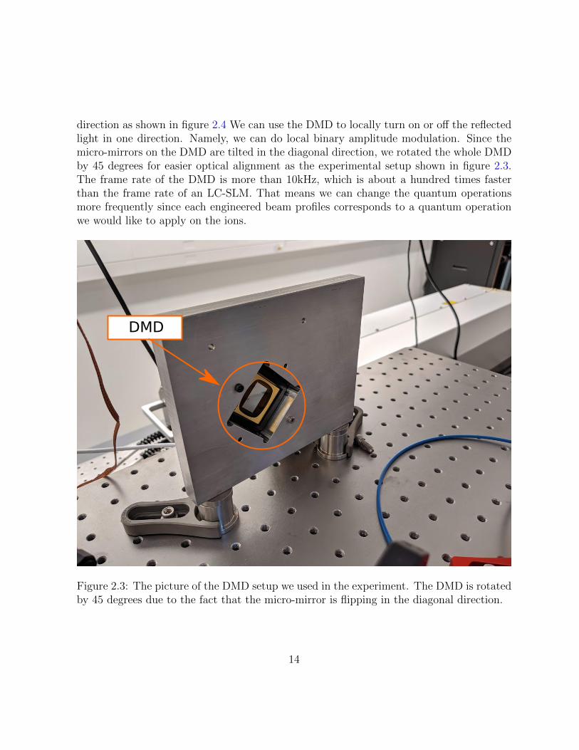
direction as shown in figure 2.4 We can use the DMD to locally turn on or off the reflectedlight in one direction. Namely, we can do local binary amplitude modulation. Since themicro-mirrors on the DMD are tilted in the diagonal direction, we rotated the whole DMDby 45 degrees for easier optical alignment as the experimental setup shown in figure 2.3.The frame rate of the DMD is more than 10kHz, which is about a hundred times fasterthan the frame rate of an LC-SLM. That means we can change the quantum operationsmore frequently since each engineered beam profiles corresponds to a quantum operationwe would like to apply on the ions.
DMD
Figure 2.3: The picture of the DMD setup we used in the experiment. The DMD is rotatedby 45 degrees due to the fact that the micro-mirror is flipping in the diagonal direction.
14

Figure 2.4: Micro-mirror landed positions and light paths. The figure is taken and editedfrom the DLP9500UV datasheet[21].
15

2.4 Off-Axis Amplitude Hologram
With a DMD, we can have binary local amplitude controls by flipping the micro-mirrors.However, to engineer an arbitrary beam profile at the image plane, we will need somecontrols on not only the amplitude of the beam profile but also its optical phase.
To understand how we engineer the beam profile with a device that can only do am-plitude modulation, let’s first relieve the constraint that the amplitude control from theDMD is binary and assume that the device has a continuous (grey scale) amplitude control.Consider we want to engineer a target beam profile f(x) which has a Fourier conjugateF (k).
F (k) = F [f(x)] (2.15)
For simplicity, we use the vector notation, x = (x, y) and k = (kx, ky).
The idea of using just the amplitude modulation to achieve both amplitude and phasecontrol is through engineering a carrier grating. If we use the diffracted beam from thegrating, we will be able to modify the phase of the light by changing the spatial phaseof the grating profiles. With this idea in mind, we can implement the amplitude gratingfunction G(k) with the following form.
G(k) =|F (k)|
2(cos(x0 · k + Φ(k)) + 1) (2.16)
whereΦ(k) = Arg(F (k)))
, and x0 defines the periodicity of the grating. Note that we add a one to the cos functionas the bias to ensure the grating function G(k) is always positive because the DMD doesn’thave the ability to invert the sign of the field (negative value of the grating in equation2.16). To verify the grating function we just constructed, we can simply apply the inverseFourier transform.
g(x) = F−1[G(k)] (2.17)
=1
4f(x− x0) +
1
4f ∗(−x + x0) +
1
2F−1[|F (k)|] (2.18)
The transformation of the function is consist of three terms, and we refer to the three termsas first, negative first, and zeroth grating order of the beam respectively. We can noticethat the first order diffraction beam has the desired beam profile yet with a shifted originat x0. Because of the shifted-origin nature of the grating-based holograms, holograms of
16

this type are usually referred to as off-axis holograms. It is worth mentioning that thenegative first order is the complex conjugate of the target beam profile. By flipping thesign of Φ(k), we can use the negative first order rather than the first order diffractionbeam. Substitute the relation between k and x (equation 2.8 and 2.9), and we will have:
G(x) =|F (x)|
2(cos(2π
x0 · xλf
+ Φ(x)) + 1)
Here we addˆon top of the function to indicate the substitution.
The grating function we’ve derived so far requires uniform illumination on the hologram,and the optical aberrations are not taken into account. However, in most of the situation,the light doesn’t illuminate the hologram uniformly and suffers from the imperfection ofthe optics. To address this problem, first, let’s denote the beam profile illuminatedshinnheDMD at the Fourier plane to be Ein(x) with aberration phase profile Φin = Arg(Ein).Although the aberrations from DMD itself and the focusing lens are not part of the Φin,we can combine all these aberrations into Φin and thus assume the DMD and the focusinglens will not introduce any optical aberrations. In the later section, we will show how tomeasure the combined aberrations phase profile for aberration compensation. With somemodification, we will able to get the grating function that can adapt to Ein.
G(x) = η
∣∣∣∣∣ F (x)
Ein(x)
∣∣∣∣∣ 1
2(cos(2π
x0 · xλf
+ Φ(x)− Φin(x)) + 1) (2.19)
with normalization constant
η = max(
∣∣∣∣∣Ein(x)
F (x)
∣∣∣∣∣) (2.20)
to make the value of G between 0 to 1. The beam profile at image plane now becomes:
Eimg(x) =2π
λfF−1[(Ein(x)G(x))|x=λf
2πk]
=2π
λfη
(1
4f(x− x0) +
1
4F−1[|F (k)|ei(−Φ(k)+2Φin(x=λf
2πk))](−x + x0)
+1
2F−1[|F (k)|eiΦin(x=λf
2πk)]
) (2.21)
As we can see in the equation, the first order beam is the aberration-free target beamprofile, but the negative first order diffraction suffers two times more aberration.
17

2.5 Binarization
Now we have the method to generate greyscale amplitude holograms that can produce thedesired beam profiles. The next step is to binarize the greyscale holograms so that theycan be displayed on the DMD. Unfortunately, binarization is a highly nonlinear process,and there is no way to do so without introducing additional error. What we can do is tryto find a binary grating function Gb(x) to approximate the grey scale grating G(x). Asan example, we show the binarized gratings with different phases and amplitudes in figure2.5.
The most trivial method to do so is to simply set up a threshold, for example, 0.5,and the value of the binarized hologram is determined by comparing the value of theunbinarized hologram with the threshold. If G(x) is greater than the threshold, Gb(x) willbe set to 1 which means the micro-mirror flips to the “on” position that will reflect thebeam to the lens.
Gb(x) =
1 if G(x) ≥ 0.5
0 if G(x) < 0.5(2.22)
However, this method gives out a significant amount of localized artifacts. Shown in figure2.6 is one of the simulation examples we made with this simple threshold method. We canobserve artifacts are lying around the target beam profile.
Increase Amplitude
Change Phase
Phase and Amplitude Control
Yellow: ONPurple: OFF
Figure 2.5: Binarized gratings with different phases and amplitudes.
18

(a)
(c)
(b)
(d)
simulated beam profile(image plane)
gratting profile(Fourier plane)
ideal gra
ting
sim
ple
thre
shold
ON
OFF artifacts
Figure 2.6: Simulation of creating TEM11 Gaussian beam profile from a fundamentalmode Gaussian beam. (a) The ideal grating profile (continuous amplitude modulation).(b) The beam profile at the image plane created with ideal grating hologram. The profileis an ideal TEM11 Gaussian beam profile. (c) The binarized amplitude grating profile.The binarization is performed with the formula in equation 2.22. (d) The beam profile atthe image plane created with the simple threshold method (equation 2.22). One can seeartifacts caused the binarization process appear in the image. Simulation condition: λ =369 nm, f = 30mm, grating periodicity = 2 pixel
To mitigate the influence of binarization errors, people have proposed several methods[12,7, 9, 26]. Shown in figure 2.7 are the simulation results with a hologram calculated with theprobabilistic algorithm from [26] and the hologram from 2.19 binarized by an error diffusion
19

algorithm [8]. We can clearly observe that the artifacts are significantly suppressed.
(a) (b)
simulated beam profile(image plane)
gratting profile(Fourier plane)
err
or
diff
usi
on m
eth
od
ON
OFF
(c) (d)
pro
babili
stic
meth
od
OFF
ON
Figure 2.7: Simulation of creating TEM11 Gaussian beam profile from a fundamentalmode Gaussian beam with improved binarization methods. (a) The binarized amplitudegrating profile created by applying the error diffusion method[8] on the ideal grating. (b)The beam profile at the image plane created with the error diffusion algorithm. (c) Thebinarized amplitude grating profile created with the probabilistic algorithm from [26] (d)The beam profile at the image plane created with the probabilistic algorithm. Simulationcondition: λ = 369 nm, f = 30mm, error diffusion algorithm: Jarvis [8], grating periodicity= 2 pixel
Before going into the details about the binarization and benchmarking the algorithms,we will first discuss what kind of profiles we are interested in. There are multiple ways of
20

engineering a target beam profile that produces the same quantum gate operation. Thebeam profile can be arbitrary as long as it has the desired values at the positions ionslocate. In other words, we only care about the beam profile close to the region that ionslocate. However, in general, we want its optical Fourier transformed profile to have a goodoverlapping with the input beam profile on the DMD, so more power of the beam can beused in addressing. More specifically, we want to maximize the normalization constant η.Since our input beam profile on the DMD is close to the fundamental Gaussian mode, wemade our addressing beam profile a series of Gaussian beams addressed on each ion.
Etarget(x) = Σiaie|x−xi|2/w2
(2.23)
Each addressing Gaussian beam satisfies the mode matching condition.
w ≈ fλ
πw0
(2.24)
where w0 is the radius of the incoming beam at which the field amplitudes fall to 1/e oftheir axial values.
To benchmark the performance of the system, we create a beam profile that has equalstrength of the light on all ions except one ion in the system. In the small figure at thebottom left of figure 2.8 shows the benchmark pattern we used. As an example, we discussthe accuracy of a six ions system. Hence, we intend to show light with equal intensities ation i = 1, 2, 3, 4, 6, while keep ion i = 5 in dark. Therefore, we can define a benchmarkmetric for the system as:
Ebenchmark(x) = Σi=1,2,3,4,6ae|x−xi|2/w2
(2.25)
We can benchmark the accuracy from the mismatch between peaks. Also, the light leakingto the position of the fifth ion indicates the crosstalk of the system. In figure 2.8, weshowed the simulation results with the two algorithms, the probabilistic algorithm and theerror-diffusion-based algorithm, along with the unbinarized (ideal) version for comparison.
21

Figure 2.8: Binarization algorithm comparison: The first row shows the grating profile atthe Fourier plane, and the second row shows the simulated normalized field amplitude atthe image plane. Simulation condition:λ = 399nm, f = 728 mm, grating periodicity = 2pixel
To examine the peak mismatch and the crosstalk, we plot the simulation results of thetwo algorithms in both linear scale and logarithmic scale in figure 2.9 and figure 2.10. Themaximum peak mismatch of both of the algorithms is around 5%. As for the crosstalk,the error diffusion method has less crosstalk. It has two to three times less cross talkthan that of the probabilistic algorithm. Both of the algorithms may be good enough forcreating arbitrary potential in some many-body quantum simulation experiment. However,comparing to the current state-of-the-art experiment [4] which has about 1% (-20dBc)crosstalk in the amplitude, we would like to find a better algorithm.
22

Figure 2.9: Simulation results of beam profile at the image plane with a hologram generatedby the probabilistic algorithm[27] (a) Normalized field amplitude. (b) Normalized fieldAmplitude in the logarithmic scale. (c) Normalized field amplitude of the cross-sectionalong the ion chain direction. (d) Normalized field amplitude of the cross-section alongthe ion chain direction in the logarithmic scale. (Simulation condition: λ = 399nm, f =728 mm, grating periodicity = 2 pixel) There is a maximum 5% peak mismatch shown infigure c and approximately -10 dBc cross-talk in figure d.
23

Figure 2.10: Simulation results of beam profile at the image plane with a hologram gener-ated by the error diffusion algorithm (a) Normalized field amplitude. (b) Normalized fieldAmplitude in the logarithmic scale. (c) Normalized field amplitude of the cross-sectionalong the ion chain direction. (d) Normalized field amplitude of the cross-section alongthe ion chain direction in the logarithmic scale. (Simulation condition: λ = 399nm, f =728 mm, grating periodicity = 2 pixel) There is a maximum 5% peak mismatch shown infigure c and approximately -15 dBc cross-talk in figure d. The cross-talk reduces by about5 dB comparing to the results in figure 2.9
24

2.6 Iterative Fourier Transform Algorithm
While looking for a better binarization algorithm, one thing we have to keep in mind isthe binarization error results from the limited degrees of freedom. Unlike the greyscalehologram which has continuous amplitude control, the DMD has only two states, on andoff. Although this means we are not able to get rid of the binarization error completely,we can try to minimize its influence by optimizing the hologram such that within a signalwindow containing the target beam profile (where the ions locate) the error is minimized.The algorithm we designed to optimize the hologram is an iterative Fourier transformalgorithm (IFTA). It is a modification of the binarization algorithm from [24].
Start: unbinarized hologram
Binarization: Project the hologram to real space and perform binarization.
Correction: Correct the beam profile within the signal window.
Fouri
er
pla
ne im
age p
lane
i = N?
Yes
No
Figure 2.11: The flowchart of our iterative Fourier transform algorithm.
25

The flow chart of our IFTA is shown in figure 2.11. In the beginning, we start with agreyscale hologram G(k) and binarized it with a binarization operator U .
G(1)b = U [G(k)] (2.26)
Since we just applied the binarization to the hologram, we will encounter the binarizationerror when we go from the Fourier plane to the image plane. The next step is to applya correction operator X which corrects the beam profile within a signal window D. Thesignal window contains the region we are interested in, for example, the ions.
g(i)c (x) = X[g(i)(x)] =
g(x) if x ∈ Dg(i)(x) otherwise
(2.27)
where g(x) is the inverse Fourier transformation of the ideal grating profile. (The targetbeam profile.)
g(x) = F−1[G(k)] (2.28)
Now the hologram at the Fourier plane is no longer binarized because we just modifiedthe profile at the image plane. Therefore, we will need to apply binarization again. Byrepeating this cycle, we will be able to reduce the error within the signal window. Thebinarization error will be “repelled” to the outside of the signal window. One may want tocorrect the first-order beam only if the edge of the signal window is near or cropping theprofile. It is because the negative first-order scattering beam suffer from optical aberrations,and the aberrations can cause the light to “leak” to the outside of the window. Correctfirst-order beam only may lead to a slower convergence speed but with lower error for thefinal result.
Note that g(i)(x) isn’t not always a real function. Therefore, we will need to project itinto real space first while performing binarization. We have tried both taking the absolutevalue and the real part of g(i)(x), and we did not find any significant difference in theconvergence speed. As a result, we use the method of taking the real part because it is lesscomputationally expensive.
To avoid stagnation and lead to a faster convergence, Wyrowski (1989) [24] suggestedusing an adaptive binarization threshold. At first, we only binarize the value close to 0and 1, and we change the binarization threshold throughout the iteration.
G(i)b = Ut[G
(i)(x)] =
0 if Re[G(i)(x)] < t
1 if Re[G(i)(x)] > t
Re[G(i)(x)] otherwise
(2.29)
26

where t is the threshold. In our algorithm, we sweep the threshold linearly through outthe iterations.
t =i
2N(2.30)
Shown in figure 2.12 is the simulation result using the IFTA with the same targetprofile used in figure 2.9 and 2.10. We can see that the peak mismatch and crosstalk aresignificantly reduced. Both of them are less than 1% now. Also, we can see in figure 2.12(b) the background error becomes less, and we have more artifacts in the area away fromthe ion positions.
27

signal window
Figure 2.12: Simulation results of beam profile at the image plane with a hologram gener-ated by the iterative Fourier transform algorithm (IFTA) (a) Normalized field amplitude.(b) Normalized field Amplitude in the logarithmic scale. (c) Normalized field amplitudeof the cross-section along the ion chain direction. (d) Normalized field amplitude of thecross-section along the ion chain direction in the logarithmic scale.(Simulation condition: λ= 399nm, f = 728 mm, N = 1500) There is a less than 1% peak mismatch shown in figurec and approximately -25 dBc cross-talk in figure d. The cross-talk reduces by about 10dB comparing to the results in figure 2.10 It also outperforms the current state-of-the-arttrapped ion quantum computer experiment[4].
28

2.7 Chapter Summary
In this chapter, we have introduced a novel algorithm to improve on holographic beamshaping. The holographic neam shaping uses a re-programmable hologram to engineerthe beam profile addressed on the ion chain. This method, compared with the existingmethods, has the following advantages.
1. With the holographic beam shaping scheme, we have control over not only the ampli-tude but also the phase of the beam. It is particularly useful if we want to engineeroptical-phase-dependent gates.
2. The holographic beam shaping scheme is immune to the imperfection of the optics.The optical aberration inside the system can be compensated by applying a correctionphase profile on the hologram.
3. Our setup is a re-programmable setup making it be able to adapt to the unequalspacing between ions in a long-chain configuration.
The device we used as the re-programmable hologram is a digital micro-mirror de-vice (DMD), a device consists of micro-mirrors that can be used as optical switches togive binarized amplitude control (on/off) on the beam profile. To use the DMD as there-programmable hologram, we need to add the binarization process to the hologram cal-culation. However, the binarization process makes unwanted artifacts occur at the imageplane. We developed a new algorithm that uses iterative Fourier transformation to opti-mize the beam profile within a region of interest in the image plane. Also, the simulationresults show less 1% inaccuracy in amplitude. The simulation shows that our algorithmhas about an order of magnitude improvement on accuracy. It also outperforms the currentstate-of-the-art trapped ion quantum computer experiment[4].
29

Chapter 3
Calibration and Use Cases
3.1 Aberration Phase Profile Measurement
One advantage of using holographic beam shaping is the ability to compensate the aber-ration, making the addressing system immune to optical imperfection. As we have shownin the 2.19, the aberration of the first-order diffraction beam can be cancelled by apply-ing a compensating phase mask while calculating the grating function. To measure theaberration phase profile, one may think of using a Shack-Hartmann wavefront sensor[13].Although it offers a straightforward method, there are some difficulties we need to dealwith. First, the size of micro-lens from a commercially available wavefront sensor is typi-cally larger than 150µm.
In contrast, the micro-mirror on the DMD is only 10.8 µm. It limits the resolution ofthe measurement. Second, there are more beams with diffraction orders, and they maynot spatially be separated until it reaches the image plane. Nevertheless, the beam profileat the image plane is small, making it not ideal for a Shack-Hartmann wavefront sensor.Also, ions are inside a vacuum chamber, making it hard to place an external sensor.
In [27], it has been demonstrated that the aberration phase profile can be measured byopening two small patches of gratings on the DMD and measuring the interference patternof the beams reflecting from the two patches. The setup is illustrated in figure 3.1. Thetwo patches are separated by a distance d. Since the patches we opened are small, thebeam profile at image plane after the optical Fourier transformation can be approximatedas a plane wave. We denoted them as E1(x) and E2(x) with optical phases φ1 and φ2
30
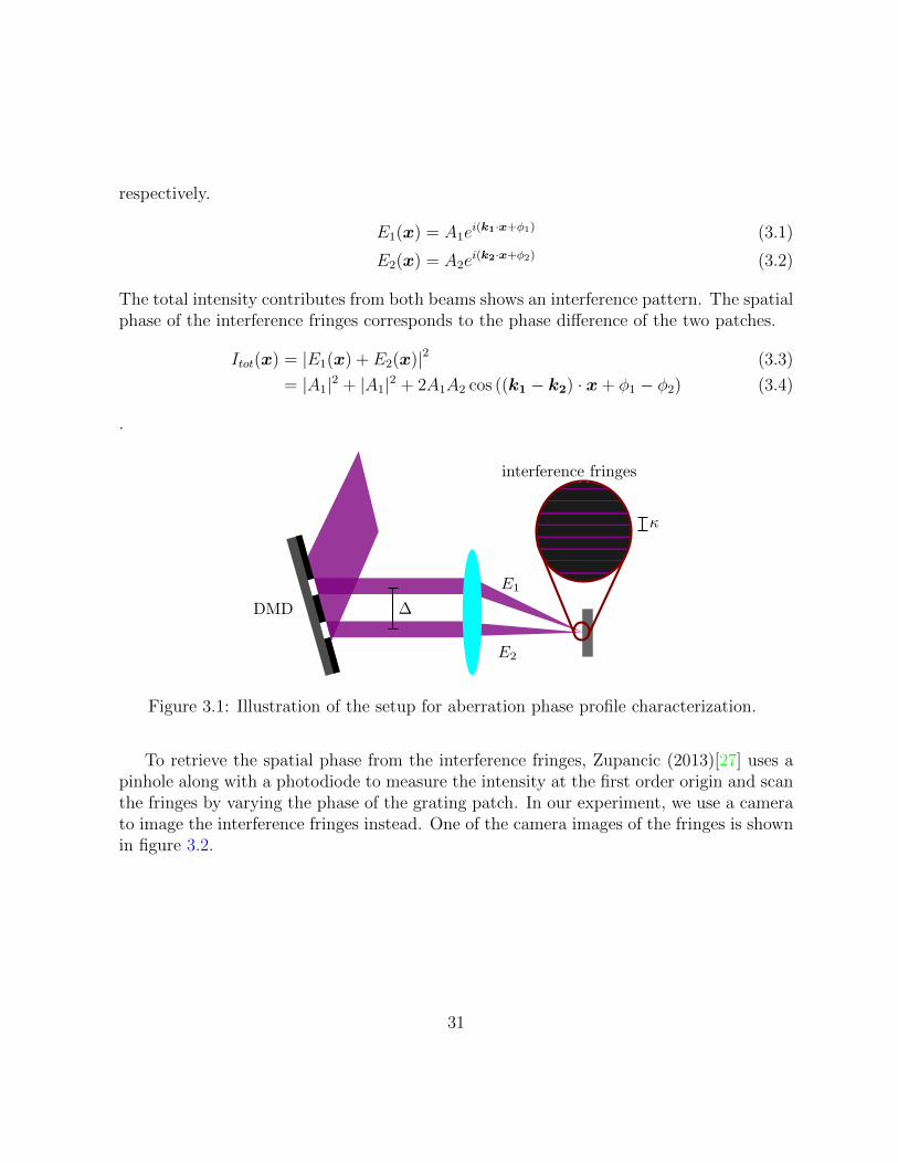
respectively.
E1(x) = A1ei(k1·x+φ1) (3.1)
E2(x) = A2ei(k2·x+φ2) (3.2)
The total intensity contributes from both beams shows an interference pattern. The spatialphase of the interference fringes corresponds to the phase difference of the two patches.
Itot(x) = |E1(x) + E2(x)|2 (3.3)
= |A1|2 + |A1|2 + 2A1A2 cos ((k1 − k2) · x + φ1 − φ2) (3.4)
.
Figure 3.1: Illustration of the setup for aberration phase profile characterization.
To retrieve the spatial phase from the interference fringes, Zupancic (2013)[27] uses apinhole along with a photodiode to measure the intensity at the first order origin and scanthe fringes by varying the phase of the grating patch. In our experiment, we use a camerato image the interference fringes instead. One of the camera images of the fringes is shownin figure 3.2.
31

Figure 3.2: A camera image of the interference pattern. camera model: BFLY-PGE-05S2M-CS, Fourier lens focal length = 500 mm
To retrieve the spatial phase of the fringe, we first sum the image over the axis whichis perpendicular to the separation direction of two patches(perpendicular to k1 − k2) andget the 1D profile f(x) after summation. The spatial phase of the interference fringesψ = φ1− φ2 can be extracted by taking the correlation1 of f(x) and a test signal eiκ(x−x0).
C = corr(eiκ(x−x0), f(x)) (3.5)
in which κ is the spatial frequency of the interference fringe. The spatial frequency dependson the separation of the two patches. Similar to the equation 2.8 and 2.9, we have:
κ = |k1 − k2| =2π
λf∆ (3.6)
where ∆ is the separation of two patches. To reconstruct the 2D phase profile, we needthe phase difference profile in two directions. By making the two patches separated alongx and y axis, we have the phase difference profile Ψx(x, y) and Ψy(x, y).
Ψx(x, y) = Φ(x+ ∆, y)− Φ(x, y) (3.7)
Ψy(x, y) = Φ(x, y + ∆)− Φ(x, y) (3.8)
1https://docs.scipy.org/doc/numpy/reference/generated/numpy.correlate.html
32

We then fit the phase profile Φ(x, y) with a series of Zernike polynomials. The result isshown in figure 3.3. We can see before aberration compensation the aberration is aboutacross the aperture is five waves. To examine the aberration compensation, we perform theexperiment again. However, we subtract the aberration phase while making the gratingpatch this time. As we can see in figure 3.4, the wavefront uniformity has been greatlyimproved. The aberration across the aperture is less than 0.1 waves, which is a 50 timesimprovement.
Aberration Phase(Fourier Plane)
Camera Image(Image Plane)
(b) (a)
Figure 3.3: Phase map of the aberration phase before aberration compensation. (a) Theaberration phase profile at the Fourier image. The aberration is about five waves across theaperture. The profile is obtained by fitting a series of Zernike polynomials up to fourth-order (The constant phase term is excluded.). (b) Camera image of Gaussian TEM11
mode created with holograph beam shaping without aberration compensation. The non-uninformed illumination results from incomplete power calibration. The wavelength weused in the experiment is 399 nm, and the radius of the aperture is 6 mm.
33

Aberration Phase(Fourier Plane)
(a)
Camera Image(Image Plane)
(b)
Figure 3.4: Phase map of the aberration phase after aberration compensation. (a) Theaberration phase profile at the Fourier image. The aberration is less than 0.1 waves acrossthe aperture. It is a 50 times improvement than the aberration before aberration com-pensation shown in figure 3.3. (b) Camera image of Gaussian TEM11 mode created withholograph beam shaping with aberration compensation. The non-uninformed illumina-tion results from incomplete power calibration. The profile is obtained by fitting a seriesof Zernike polynomials up to fourth-order (The constant phase term is excluded.). Thewavelength we used in the experiment is 399 nm, and the aperture radius is 6 mm.
3.2 Aberration Calibration with An Ion
In section 3.1, we have discussed how to measure the aberration phase profile with a cameraplaced in the image plane and demonstrated that it could be compensated. However,when we use it as an addressing apparatus for ions, the final image plan is inside thevacuum chamber, which may make it unreachable with conventional sensors. Hence, weproposed the idea of using a trapped ion as the sensor. To do so, we need the ability tomeasure the intensity of the light at the ion position and a way to scan the interferencefringes. For an off-resonance beam, the power measurement can be done by measuringthe differential AC Stark shift between two-qubit states with standard techniques such as
34

Ramsey spectroscopy. As for the resonance beam, we can measure the power from thefluorescence of the ion. To scan the interference fringes, we can use either of the twomethods:
1. Changing the DC voltages on the electrodes to move the ion across the trap.
2. Deploy a piezo-controlled mirror on the Fourier plane. The tilt of the mirror corre-sponds to the transnational displacement on the image plane.
3.3 Maximizing Diffraction Efficiency
The mirror array on the DMD itself forms a grating that that can diffract the light intonot just one of the two directions. The interference pattern from the micro-mirror arraygrating comes with an envelope which is defined by the diffraction pattern from a singlemicro-mirror. Note that the grating we are talking here is not the grating profile wehave discussed in the equation 2.19, the grating here comes from the periodic structure ofthe micro-mirror array. As figure 3.5 shows, each diffracted beam from the micro-mirrorgrating contains beams of the three diffraction orders from the hologram grating.
35

Figure 3.5: Illustration of multiple diffraction beams from the micro-mirror array grating.(a) Each diffraction beam from the micro-mirror array grating has three diffraction orderbeams from the hologram grating. (b) The law of reflection of micro-mirrors.
To maximize the diffraction efficiency of the DMD, we want the envelope to overlapwith the diffraction beam we are interested in, so we can channel more power to the targetbeam profile. The center of the diffraction envelope satisfies the law of reflection of a singlemirror.
β = −α− 2θ (3.9)
where α and β are the incident angle respectively, and θ is the tilt angle of the micro-mirrorwhich is 12 degrees in our DMD. As for the micro-mirror grating, it follows the gratingequation.
sinα + sin β =
√2nλ
d(3.10)
Here, n states the diffraction order of the mirror-mirror grating, and d is the edge length ofa micro-mirror. The
√2 factor comes from the fact that the micro-mirror is flipped along
36

the diagonal axis. (Figure 2.4). Combine equation 3.9 and equation 3.10, we get:
sinα + sin (−α− 2θ) =
√2nλ
d(3.11)
We solve the equation numerically, and the results are shown in figure 3.6 where thezero-crossing points are. There are multiple solutions depends on the diffraction order wechoose. In our experiment, we use the -8th diffraction order because the reflection angle βis close to 0 degree and it has less distortion from tilt.
Figure 3.6: Solutions for equation 3.11 with different diffraction order. The solutionsindicates the condition of maximized diffraction efficiency. The solutions are at the zerocrossing points. The solutions exist between zeroth order to negative eighth order. Foreach order, there will be two solutions. Condition: d = 10.8 um, λ = 369nm
3.4 Use case: Linear Gradient Intensity
An application of individual addressing is arbitrary single-qubit phase gates. We can useoff-resonance beams to induce different amounts of phase shift to different qubits with theAC Stark shift effect.
37

To understand the AC Stark shift, first, we consider a two-level system as figure 3.7shows. The energy separation between ground state |g〉 and excited state |e〉 is ωe. (letting~ = 1) The two states are off-resonantly coupled with a laser with frequency ω and Rabifrequency Ω. The laser is detuned ∆ from the transition. We can write the Hamiltonianof the system as the following equation.
H =ωe2|e〉 〈e| − ωg
2|g〉 〈g|+ Ω
2(|e〉 〈g|)(eiωt + e−iωt) + h.c. (3.12)
We can bring the Hamiltonian to the laser rotating frame.
Hrot = eiH0t(H −H0)e−iH0t (3.13)
= −∆
2|e〉 〈e|+ ∆
2|g〉 〈g|+ Ω
2(|e〉 〈g|)(ei2ωt + 1) + h.c. (3.14)
whereH0 =
ω
2|e〉 〈e| − ω
2|g〉 〈g| (3.15)
. We can ignore the fast rotating term ei2ωt in equation 3.14 with the rotating waveapproximation (RWA).
Hrot ≈ −∆
2|e〉 〈e|+ ∆
2|g〉 〈g|+ Ω
2(|e〉 〈g|) + h.c. (3.16)
As we can see now, the Hamiltonian is time independent. By diagonalizing the Hamilto-nian, we can obtain the eigen states and their energy. With the assumption that ∆ Ω,we have the new eigen energies become:
Erot = ±√
∆2
4+
Ω2
4(3.17)
≈ ±(
1
2∆ +
Ω2
4∆
)(3.18)
Comparing with equation 3.16, we can find that 12∆ + Ω2
4∆corresponds to the energy of the
shifted ground state, and the other one corresponds to the energy of the shifted excitedstate. We can find the energy shift is proportional to the square of Ω.
δEg = +Ω2
4∆(3.19)
δEe = −Ω2
4∆(3.20)
38

For a multi-level system, the total AC Stark shift are the sum over the contributions fromall the excited states.
δEg =∑i
Ω2i
4∆i
=g2
0
4
∑i
B2i
∆i
(3.21)
where B is the branching ration and g20 = Γ2 Ilaser
2Isat. Γ is the nature linewidth of the
transition. Ilaser is the intensity of the laser, and Isat is the saturation intensity.
Figure 3.7: AC Stark shift in a two-level system.
As figure 3.8 shows, for 171Yb+, most of the contributions are from 2P1/2 and 2P3/2
excited states. We can calculate the AC Stark Shift of the two-qubit states. (The branchingratio calculations are in appendix A.) For the beam with arbitrary polarization, the energy
39

shifts of the two-qubit states are:
δE0 =g2
0
12
(1
∆− 2
ωF −∆
)(3.22)
δE1 =g2
0
12
(1
∆ + ωHF− 2
ωF −∆− ωHF
)(3.23)
Figure 3.8: AC Stark shift of 171Yb+.
We can find difference energy shifts from the two-qubit states contributes to a non-zerodifferential AC Stark shift.
δωqubit = δE0 − δE1 (3.24)
which is proportional to the intensity of the laser.
ωqubit ∝ g20 ∝ Ilaser (3.25)
40

Therefore, we can have addressing patterns that have different intensity on different ions.With the same amount of the operation time, the phase shift is proportional the localintensities.
As an example, figure 3.9 shows a linear intensity gradient intensity profile we createdwith the holographic beam shaping. This particular example can be used in our theoryproposal[15] in which global Mølmer-Sørensen gates and arbitrary single-qubit phase gatesare used to simulate 2D lattices in a hybrid digital-analog way.
~5 Airy disc radius
inte
nsi
ty (
arb
. unit
s)
Camera Image
Figure 3.9: A linear gradient intensity pattern created by holographic beam shaping. λ= 399 nm. It can be used to create site-dependent phase shifts that can be used in thequantum simulation experiment from Rajabi et al. (2019)[15]
3.5 Chapter Summary
In this chapter, we discussed some important considerations for implementing the holo-graphic beam shaping scheme that has been proposed in chapter 2.
41

1. Maximizing Efficiency: The micro-mirror array itself acts as a grating that createsmultiple diffracted beams. Each diffraction order contains the negative first, zeroth,and first diffraction order from the hologram grating. The diffracted angles of thebeams follow the grating equation. On top of the diffraction patterns from thegrating, there is an envelope which corresponds to the diffraction pattern of a singlemicro-mirror. The center of the envelope where it also has the maximum value followsthe law of reflection. To channel as much as energy possible to the beam with thedesired diffraction order, one needs to find a proper input angle such that the centerof the envelope aligns with the beam. The angle can be found by solving the gratingequation and the law of reflection at the same time.
2. Aberration Compensation: In the previous chapter, we have shown the optical aber-ration can be compensated by applying a correction phase profile while calculatingholograms. To find the correction phase profile, we need to characterize the opticalaberration in the system. We showed that the aberration phase could be measuredby opening two patches on the DMD. The beams from the two patches overlap atthe image forming interference fringes. The spatial phase of the interference fringescorresponds to the phase difference between the two patches. By shifting the patchesacross the DMD, we can reconstruct the aberration phase profile. We also discussedthe plan to use a single ion as a detector to measure the interference fringes at thefinal image plane when we integrate the system to an ion trap in the future.
Along with the experimental considerations, we also show a use case of holographic beamshaping. In this use case, we engineer a linear gradient intensity profile that can beconverted to phase shifts on the ions through the AC Stark shift. It can be used inour recent theoretical proposal[15] which simulates the dynamics of 2D lattices in a linearchain of ions.
42

Chapter 4
Holographic Addressing withMultiple Frequency Channels
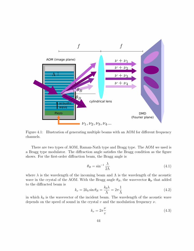
As we discussed in section 1.2, it is required to have the individual addressing ability ofbeams with different frequencies to have full control over the spin-spin interaction graph.As the schematic in figure 4.1 show, an AOM combining with a cylindrical convex lens isused to split the light onto different zones of the DMD. These zones correspond to differentRF input frequencies. They act as different frequency channels. Each channel has itshologram for controlling the amplitudes and phases of the beams addressed on individualions.
43
Piezo
acousticwave
AOM (image plane)
DMD(Fourier plane)
cylindrical lens
Figure 4.1: Illustration of generating multiple beams with an AOM for different frequencychannels.
There are two types of AOM, Raman-Nath type and Bragg type. The AOM we used isa Bragg type modulator. The diffraction angle satisfies the Bragg condition as the figureshows. For the first-order diffraction beam, the Bragg angle is
θB = sin−1 λ
2Λ(4.1)
where λ is the wavelength of the incoming beam and Λ is the wavelength of the acousticwave in the crystal of the AOM. With the Bragg angle θB, the wavevector kν that addedto the diffracted beam is
kν = 2k0 sin θB =k0λ
Λ= 2π
1
Λ(4.2)
in which k0 is the wavevector of the incident beam. The wavelength of the acoustic wavedepends on the speed of sound in the crystal v and the modulation frequency ν.
kν = 2πν
v(4.3)
44

The wavevector kν is along the propagation direction of the acoustic wave which is almostperpendicular to the propagation direction of the beam. The frequency of the diffractedbeam also depends on the modulation RF frequency. For the first-order diffraction beam,the modulation frequency is added to the frequency of the beam. As a result, by applyingmultiple-tone RF to the AOM, we can split a beam into several beams, and each of themhas a different frequency detuning.
∆kν = 2π∆ν
v(4.4)
To determine what the minimum frequency splitting is required for avoiding the crosstalkbetween the adjacent frequency channels, we will need to know the beam waist of thediffracted beam. Consider an incident Gaussian beam with wait radius w0, its Fouriertransform shows.
F [e− x2
w20 ] ∝ e
− k2
(2/w0)2 = e
− k2
k2w (4.5)
It reveals that the waist radius of the Gaussian beam in Fourier space kw is inverse pro-portional to the beam waist.
kw =2
w0
(4.6)
Assume the minimum separation to be γ times of the waist radius.
∆kν = γkw (4.7)
We can find the required frequency difference.
∆ν = γv
πw0
(4.8)
For a given γ, it only depends on the dimension of the incident beam and the materialproperty of the crystal. The materials commonly used as the crystal in the AOM aretellurium dioxide, fused silica, germanium, and quartz. However, not all of them have goodtransmission efficiency in the UV spectrum. As a result, we use an AOM from IntraactionInc. which use fused silica. The speed of sound in fused silica is about 5968 m/s [23]. Inour experiment, we choose to have at least a 2MHz separation between frequency channels.
4.1 Frequency Channels Preparation
In the previous section, we described the method of generating multiple beams with dif-ferent frequencies illuminating different zones of the DMD. One thing we have to be aware
45

of is that it implies the Fourier plane is divided, and each beam only takes a part of theFourier plane in order not to overlap with other beams. As a consequence, this limits theability to generate diffraction-limited profiles at the image plane. The size of the profileeach beam can generate is roughly inverse proportionally to the size of the occupied areain the Fourier plane. To get around with this problem, we introduce cylindrical lenses intothe system. We shape the beams to make them have elliptical shapes on the DMD. Thebeams are separated along the short axis and expand across the Fourier plane along thelong axis. The long axis of the beam on the DMD corresponds to the axial direction ofthe ion chain, and the shot axis corresponds to the radial direction. Although generatingdiffraction-limited spots with multiple frequencies is still unavailable with this setup dueto the fundamental limitation of the segmented Fourier plane, we can achieve diffraction-limited addressing along the axial direction by increasing the beam waist at the Fourierplane along this direction.
Figure 4.2 is the schematic of the optics we built to prepare these elliptical beams. (Thepicture of the setup is shown in figure 4.2) We first expand the beam in the horizontaldirection before the AOM with a telescope which is made of cylindrical lenses. The AOMsplits the light into multiple beams. The neighbouring beams have a 2 MHz difference infrequency.
After the AOM, the beam will pass through a cylindrical lens which serves the samepurpose as the lens in figure 4.1. The center of the AOM is placed at the focal plane of thecylindrical lens, making the angular separation of beams converted to the transnationalseparation. The only difference is we have a cylindrical telescope and a telescope to shapethe beams to the proper size before them land the DMD. As figure 4.2 (a) shows, thebeams are elliptical on the DMD. The long axis is along the vertical direction. It is alsonoteworthy that we put the AOM at another image plane relative to the DMD, so the beamof different frequencies will be combined at the camera position (image plane) without theneed to add extra phase gradient on the hologram.
In summary, we segmented the Fourier plane into several areas and illuminated eacharea with a beam with different frequency. They are acting as different frequency chan-nels. Each of the channels has its hologram for amplitude modulation and phase control.Although the Fourier plane is segmented, we still have the beam to span across the Fourierplane along the ion chain direction. It enables us to have diffraction-limited addressing inthis direction.
46

7x telescope
• Edmund Optics
• #35-109
DMD
(Fourier Plane)
AOM
• Intraaction
• ASM-2002B8
Camera
(Image Plane)
• FLIR
• BFS-PGE-120S4M
f = -30• Thorlabs• LK1982L1-A
f=200
• Thorlabs
• LA4984-UV
f = 200• Thorlabs• LJ1653L1-A
f = -30• Thorlabs• LK1982L1-A
f = 200• Thorlabs• LJ1653L1-A
f = 100• Thorlabs• LJ1567L1-A
initial beam diameter = 1.2
unit: mm
Figure 4.2: Schematic of the optical setup for the multi-frequency addressing scheme. Thecylindrical optics which shapes the beams in horizontal directions uses the red colour inthe schematic.
47

DMD(Fourier Plane)
AOM
Camera (intermediate image plane)
Fourier lens
cylindrical lens
cylindrical lens
7x telescope
Figure 4.3: Picture of the optical setup for the multi-frequency addressing scheme. Thepurple arrows indicates the beam path. The schematic of the setup is shown in figure 4.2
4.2 Experiment Results
Shown in figure 4.4 is the intensity profile of a frequency channel on the DMD. Notethat the DMD is rotated at 45 degrees, so the long axis of the beam is along the verticaldirection. The 1/e2 width of the beam in the horizontal direction (short axis) is around100 µm to 200 µm. The intensity profile is by turning on patches of mirrors and measurethe intensity of the light from the reflection.
48

ion chain direction
mircro-m
irror pixel
mirc
ro-m
irror
pixel
Normalized Intensity
frequency control
Figure 4.4: Intensity profile of the beam of a frequency channel on the DMD. The size ofa micro-mirror pixel is 10.8 µm x 10.8 µm.
To measure the aberration phase, we use the techniques described in section 3.1. Thedifference is that we fixed one of the patches at the center of the aperture, and scan
49

the other patch along the long axis direction. The results are fitted with a third-orderpolynomial and are shown in figure 4.5.
Figure 4.5: Aberration phase profile of the beam along the long axis of a frequency channelon the DMD. The profile is fitted to a third-order polynomial.
To demonstrate we can use the scheme for ion addressing, we create a profile that canbe used to address all ions except the third one for a four-ion system. Figure 4.6 shows theintensity profile at the image plan taken by a camera. The binarization method we use isIFTA with the signal window spanning from about 350 to 700 camera pixel in the verticaldirection and 450 to 550 camera pixel in the horizontal direction. Note that the ion chaindirection corresponds to the vertical direction. Note that the long axis of a cylindricalbeam at the Fourier plane will become short axis in the image plane.
The crosstalk is around -30 dB in intensity which corresponds to about -15 dB in fieldamplitude. Comparing to our simulation results which show having crosstalk around -20dB, we think the experiment can be improved by further optimizing the aberration phaseprofile measurements with a full 2D scan.
50

signal window
Figure 4.6: The camera image of an addressing profile shaped from one frequency channel.The green box shows the boundary of the signal window, and the blue dots indicate theposition of addressing targets. The experimental result shows it has less than -30db dBccrosstalk in intensity of light. Binarization method: IFTA, camera pixel size: 1.85 µm x1.85 µm
4.3 Chapter Summary
To have full control over spin-spin interaction between ions, we need to have frequencycontrol over the laser beams. We proposed and demonstrated a scheme that adding fre-
51

quency control to the holographic beam shaping scheme. The frequency is implementedwith an AOM. The AOM splits the light onto multiple zones on the DMD, and the light oneach zone has a different frequency which depends on the RF frequency fed to the AOM.Each zone acts as a frequency channel, and a hologram is displayed on it for modulatingthe beam of the frequency channel.
In this chapter, we discussed the criteria to separate the beams between adjacent chan-nels for illuminating different zones of the DMD. We found it depends on the size of theinput beam for the AOM and the material used as the crystal in the AOM. We builtan optics setup for preparing frequency channels. Several pieces of cylindrical optics areused in setup, making the beams illuminated on the DMD has an elliptical shape. Itmakes the beams still span across the Fourier plane to achieve diffraction-limited address-ing while segmenting the Fourier plane for frequency control. Finally, we demonstratedmaking aberration-corrected addressing beams created from a single frequency channel.The experimental results show a -30dB crosstalk in intensity.
52

Chapter 5
Summary and Outlook
In summary, we have developed a binarization algorithm that is optimized for creatingaddressing profiles in the trapped ion system. The algorithm shows an order of magnitudeimprovement in increasing the accuracy. We also experimentally demonstrated aberrationcompensation and holographic beam shaping experimentally in the ultra-violet wavelengthsuitable for 171Yb+. The UV wavelength is more sensitive to the environment perturbationthan the visible or IR due to its short wavelength. We experimentally demonstrate thatthe wavefront flatness could be corrected to less than 0.15 waves across a Fourier planeaperture of 6mm diameter.
Also, we developed a scheme for adding frequency control to the holographic beamshaping addressing system. By using an AOM to separate the light and illuminating dif-ferent zones on the DMD, we can simultaneously address ions with beams having differentfrequencies. It can be handy for engineering Ising spin-spin interaction with the Mølmer-Sørensen scheme[10].
For future integrating the holographic beam shaping techniques to the ion trap wehave, we plan to use a single ion as a sensor for calibrating the aberration from opticsincluding the microscope objective since the final image plane locates insides the Vacuumchamber that is not reachable with a conventional device. More discussions on the planare in section 3.2.
Another challenge for integrating the holographic beam shaping system to an ion trapis the use of picosecond pulsed laser. It is commonly to pulsed laser for the operation oftwo-photon Raman transition in order to cover the hyperfine splitting in electronic statesof nonzero nuclear spin ions [4]. The use of picosecond pulsed laser simplifies the need forpreparing another mode-locked laser. However, the broadened frequency due to the finite
53

pulse width can cause the broadening of the beam profile at the image plane. It is becausethe scaling between wavevectors at the Fourier plane and distances at the image plane iswavelength-dependent. The problem can be mitigated by reducing the micro-mirror arraydiffraction order of the beam shown in figure 3.5. The detailed analysis can be found inappendix B.
In the future, we plan to install the setup on our ion trap apparatus, and use it to en-gineer various types of spin-spin interactions between qubit spin states for future quantumsimulation experiments, for example, simulating different types of 2D lattices[15].
54

References
[1] Jacob Biamonte, Peter Wittek, Nicola Pancotti, Patrick Rebentrost, Nathan Wiebe,and Seth Lloyd. Quantum machine learning. Nature, 549(7671):195, 2017.
[2] Alexander Braun. Addressing Single Yb 1hn+ Ions: A New Scheme for QuantumComputing in Linear Ion Traps;[Experimente Durchgefuhrt Am Institut Fur Laser-Physik Der Universitat Hamburg]. Cuvillier Verlag, 2007.
[3] Juan I Cirac and Peter Zoller. Quantum computations with cold trapped ions. Physicalreview letters, 74(20):4091, 1995.
[4] Shantanu Debnath, Norbert M Linke, Caroline Figgatt, Kevin A Landsman, KevinWright, and Christopher Monroe. Demonstration of a small programmable quantumcomputer with atomic qubits. Nature, 536(7614):63, 2016.
[5] Jurgen Eschner, Giovanna Morigi, Ferdinand Schmidt-Kaler, and Rainer Blatt. Lasercooling of trapped ions. JOSA B, 20(5):1003–1015, 2003.
[6] Alexander L Gaunt and Zoran Hadzibabic. Robust digital holography for ultracoldatom trapping. Scientific reports, 2:721, 2012.
[7] Richard Hauck and Olof Bryngdahl. Computer-generated holograms with pulse-density modulation. JOSA A, 1(1):5–10, 1984.
[8] John F Jarvis, C Ni Judice, and WH Ninke. A survey of techniques for the display ofcontinuous tone pictures on bilevel displays. Computer graphics and image processing,5(1):13–40, 1976.
[9] Dieter Just, Richard Hauck, and Olof Bryngdahl. Rational carrier-period for bina-rization of sampled images and holograms. Optics communications, 60(6):359–363,1986.
55
[10] Simcha Korenblit, Dvir Kafri, Wess C Campbell, Rajibul Islam, Emily E Edwards,Zhe-Xuan Gong, Guin-Dar Lin, Lu-Ming Duan, Jungsang Kim, Kihwan Kim, et al.Quantum simulation of spin models on an arbitrary lattice with trapped ions. NewJournal of Physics, 14(9):095024, 2012.
[11] Aaron C Lee, Jacob Smith, Philip Richerme, Brian Neyenhuis, Paul W Hess, JiehangZhang, and Christopher Monroe. Engineering large stark shifts for control of individualclock state qubits. Physical Review A, 94(4):042308, 2016.
[12] Wai-Hon Lee. Binary computer-generated holograms. Applied Optics, 18(21):3661–3669, 1979.
[13] Ben C Platt and Roland Shack. History and principles of shack-hartmann wavefrontsensing. Journal of refractive surgery, 17(5):S573–S577, 2001.
[14] MG Raizen, JM Gilligan, James C Bergquist, Wayne M Itano, and David J Wineland.Ionic crystals in a linear paul trap. Physical Review A, 45(9):6493, 1992.
[15] Fereshteh Rajabi, Sainath Motlakunta, Chung-You Shih, Nikhil Kotibhaskar, QudsiaQuraishi, Ashok Ajoy, and Rajibul Islam. Dynamical hamiltonian engineering of 2drectangular lattices in a one-dimensional ion chain. npj Quantum Information, 5(1):32,2019.
[16] Philipp Schindler, Daniel Nigg, Thomas Monz, Julio T Barreiro, Esteban Martinez,Shannon X Wang, Stephan Quint, Matthias F Brandl, Volckmar Nebendahl, Chris-tian F Roos, et al. A quantum information processor with trapped ions. New Journalof Physics, 15(12):123012, 2013.
[17] Marlan O Scully and M Suhail Zubairy. Quantum optics, 1999.
[18] Peter W Shor. Algorithms for quantum computation: Discrete logarithms and factor-ing. In Proceedings 35th annual symposium on foundations of computer science, pages124–134. Ieee, 1994.
[19] Anders Sørensen and Klaus Mølmer. Quantum computation with ions in thermalmotion. Physical review letters, 82(9):1971, 1999.
[20] Daniel A Steck. Quantum and atom optics, volume 47. 2007.
[21] Texas Instrument. DLP9500UV DLP® 0.95 UV 1080p 2x LVDS Type A DMD, 112014. REVISED MARCH 2017.
56

[22] Ye Wang, Mark Um, Junhua Zhang, Shuoming An, Ming Lyu, Jing-Ning Zhang, L-M Duan, Dahyun Yum, and Kihwan Kim. Single-qubit quantum memory exceedingten-minute coherence time. Nature Photonics, 11(10):646, 2017.
[23] Robert C Weast, Melvin J Astle, William H Beyer, et al. CRC handbook of chemistryand physics, volume 69. CRC press Boca Raton, FL, 1988.
[24] Frank Wyrowski. Iterative quantization of digital amplitude holograms. Applied op-tics, 28(18):3864–3870, 1989.
[25] Wang Ye, Zhang Jing-Ning, and Kim Kihwan. Single-ion qubit with coherence timeexceeding 10 minutes. ACTA PHYSICA SINICA, 68(3), 2019.
[26] Philip Zupancic, Philipp M Preiss, Ruichao Ma, Alexander Lukin, M Eric Tai,Matthew Rispoli, Rajibul Islam, and Markus Greiner. Ultra-precise holographic beamshaping for microscopic quantum control. Optics express, 24(13):13881–13893, 2016.
[27] Philip PJ Zupancic. Dynamic holography and beamshaping using digital micromirrordevices. LMU Munich, Grainer Lab Harvard, 242, 2013.
57

APPENDICES
58
Appendix A
Branching Ration of D1 and D2 Linein 171Yb+
To calculate AC Stark shift (section 3.4), we need to incorporate branching of D1 and D2Line in 171Yb+. To calculate the branching ratios for the sub-level Rabi frequencies Ω, wewill need to calculate all the components of dipole matrix elements. With Wigner-Eckarttheorem, we can separate the angular dependiencies of the dipole matrix element. The
first term⟨F∣∣∣∣∣∣~d∣∣∣∣∣∣F⟩ is reduced dipole matrix element, and the second term CGFe,me
Fg ,mg ;1,q is
the Clebsch-Gordan coefficant.
〈Fe|dq|Fg〉 =⟨Fe
∣∣∣∣∣∣~d∣∣∣∣∣∣Fg⟩ 〈Fe,me〉Fg,mg; 1, q =⟨Fe
∣∣∣∣∣∣~d∣∣∣∣∣∣Fg⟩CGFe,meFg ,mg ,1,q
(A.1)
However, the quantum number F raises from the coupling of the net orbital angularmomentum J and the nuclear spin I. The dipole operator ~d refers to the position of theelectron which couples to J only. As a result, we need to futher processed the reduceddipole matrix element.⟨
Fe
∣∣∣∣∣∣~d∣∣∣∣∣∣Fg⟩ = (−1)Fe+I+Jg+1√
(2Fg + 1) (2Je + 1)
Jg Je 1Fe Fg I
⟨Je
∣∣∣∣∣∣~d∣∣∣∣∣∣Jg⟩ (A.2)
where the curly bracket ... is the Wigner 6-j symbol.[20] For Ytterbium 171, thenuclear spin quantum number is 1
2. With the definition of the Rabi frequency, we know the
59

Rabi frequency (proportional to the dipole matrix element) with polarization q will be:
Ω(q) = (−1)Fe+12
+Jg+1√
(2Fg + 1) (2Je + 1)CGFe,meFg ,mg ,1,q
Jg Je 1Fe Fg
12
g0 (A.3)
= BJe,Fe,meFg ,mg ;1,qg0 (A.4)
where g0 = Γ2 Ilaser2Isat
and BJe,Fe,meFg ,mg”;1,q is the branching ratio. Γ is the nature linewidth. Ilaser
is the intensity of the laser, and Isat is the saturation intensity.
For D1 line transitions (2P1/2 excited states), the non-zero branching ratios are:
B1/2,1,−10,0;1,−1 = −
√3
3(A.5)
B1/2,1,−11,0;1,−1 =
√3
3(A.6)
B1/2,1,01,1;1,−1 =
√3
3(A.7)
B1/2,0,01,1;1,−1 =
√3
3(A.8)
B1/2,1,00,0;1,0 = −
√3
3(A.9)
B1/2,1,−11,−1;1,0 = −
√3
3(A.10)
B1/2,0,01,0;1,0 = −
√3
3(A.11)
B1/2,1,11,1;1,0 =
√3
3(A.12)
B1/2,1,10,0;1,1 = −
√3
3(A.13)
B1/2,1,01,−1;1,1 = −
√3
3(A.14)
B1/2,0,01,−1;1,1 =
√3
3(A.15)
B1/2,1,11,0;1,1 = −
√3
3(A.16)
60

For D2 line transitions (2P3/2 excited states), the non-zero branching ratios are:
B3/2,1,−10,0;1,−1 =
√6
3(A.17)
B3/2,2,−21,−1;1,−1 = 1 (A.18)
B3/2,2,−11,0;1,−1 =
√2
2(A.19)
B3/2,1,−11,0;1,−1 =
√6
6(A.20)
B3/2,2,01,1;1,−1 =
√6
6(A.21)
B3/2,1,01,1;1,−1 =
√6
6(A.22)
B3/2,1,00,0;1,0 =
√6
3(A.23)
B3/2,2,−11,−1;1,0 =
√2
2(A.24)
B3/2,1,−11,−1;1,0 = −
√6
6(A.25)
B3/2,2,01,0;1,0 =
√6
3(A.26)
B3/2,2,11,1;1,0 =
√2
2(A.27)
B3/2,1,11,1;1,0 =
√6
6(A.28)
B3/2,1,10,0;1,1 =
√6
3(A.29)
B3/2,2,01,−1;1,1 =
√6
6(A.30)
B3/2,1,01,−1;1,1 = −
√6
6(A.31)
B3/2,2,11,0;1,1 =
√2
2(A.32)
B3/2,1,11,0;1,1 = −
√6
6(A.33)
B3/2,2,21,1;1,1 = 1 (A.34)
61

Appendix B
Holographic Beam Shaping withPulsed Laser
In a trapped-ion quantum simulator, it is common to do individual addressing with pulsedlasers. The main reason to use a pulsed laser is that we can use two comb teeth in thefrequency domain to couple the two-qubit states. It saves the requirement of having twomode-lock lasers while performing Raman transition. Also, the pulsed laser can be usedto generate differential fourth-order AC Stark shift.[11] Unlike the second-order AC Starkshifts shown in equation 3.22 and 3.23 that shift in the same direction, the fourth-orderAC Stark shifts of the two-qubit states are shifted in the opposite direction. It may giveus a larger phase shift with a sufficient amount of power.
However, there are extra things to consider while using holographic beam shaping onthe pulsed laser. We know the position of the beam is wavelength dependent, and theshort pulse width makes the frequency comb tooth spans over the frequency domain. Toestimate the broadening of the beam profile from the effect, we first consider the separationbetween zeroth and n-th micro-mirror grating order is:
|x(n)0 | = n
√2λf
D(B.1)
where d is the edge length of the micro-mirror. The√
2 term comes from the fact that themirror is flipping along the diagonal direction. The details of diffraction from micro-mirrorgrating is in section 3.3. The broadening results from the short pulse width gives us:
δx = n√
2f
dδλ (B.2)
62

On the other hand, the diameter of the profile at the image plane Di is roughly inverseproportional to the diameter at the Fourier plane Df .
Di =λf
Df
(B.3)
The relation between wavelength λ and laser frequency ν is:
δλ =λ
νδν (B.4)
The frequency span δν is basically one over the pulsed width. With equation B.2, B.3,and B, we can get the ratio between δx and Di.
r =δx
Di
= n√
2Df
d
δν
ν(B.5)
This ratio indicates the broadening relative to the size of the profile at the image plane.Below is the parameter of the laser used in our lab. Ideally we want to make it smallerthan one. (The smaller the better) With n = 8 and the parameter of the pulsed laser inour lab,
ν = 844THz (B.6)
δν = 1/(15ps) = 67GHz (B.7)
Df = 500d (B.8)
, we have r ≈ 0.4. The number isn’t much less than one. We might want to use a smallern if we want to use the pulsed laser.
63