Helium-Ion-Induced Radiation Damage in LiNbO_3 Thin Film Electro-Optic Modulators
9
Helium-ion-induced radiation damage in LiNbO 3 thin-film electro-optic modulators Hsu-Cheng Huang, 1,* Jerry I. Dadap, 2 Girish Malladi, 3 Ioannis Kymissis, 1 Hassaram Bakhru, 3 and Richard M. Osgood, Jr. 1,2 1 Department of Electrical Engineering, Columbia University, New York, New York, 10027, USA 2 Department of Applied Physics and Applied Mathematics, Columbia University, New York, New York, 10027, USA 3 College of Nanoscale Science and Engineering, SUNY at Albany, Albany, New York 12203, USA * [email protected] Abstract: Helium-ion-induced radiation damage in a LiNbO 3 -thin-film (10 ȝm-thick) modulator is experimentally investigated. The results demonstrate a degradation of the device performance in the presence of He + irradiation at doses of 10 16 cm 2 . The experiments also show that the presence of the He + stopping region, which determines the degree of overlap between the ion-damaged region and the guided optical mode, plays a major role in determining the degree of degradation in modulation performance. Our measurements showed that the higher overlap can lead to an additional ~5.5 dB propagation loss. The irradiation-induced change of crystal-film anisotropy ( ) o e n n of ~36% was observed for the highest dose used in the experiments. The relevant device extinction ratio, V π L, and device insertion loss, as well the damage mechanisms of each of these parameters are also reported and discussed. ©2014 Optical Society of America OCIS codes: (130.3730) Lithium niobate; (160.2100) Electro-optical materials; (230.2090) Electro-optical devices; (230.4110) Modulators. References and links 1. L. Arizmendi, “Photonic applications of lithium niobate crystals,” Phys. Status Solidi A 201(2), 253–283 (2004). 2. M. Levy, R. M. Osgood, R. Liu, L. E. Cross, G. S. Cargill, A. Kumar, and H. Bakhru, “Fabrication of single- crystal lithium niobate films by crystal ion slicing,” Appl. Phys. Lett. 73(16), 2293 (1998). 3. P. Rabiei and P. Gunter, “Optical and electro-optical properties of submicrometer lithium niobate slab waveguides prepared by crystal ion slicing and wafer bonding,” Appl. Phys. Lett. 85(20), 4603–4605 (2004). 4. P. Rabiei, J. Ma, S. Khan, J. Chiles, and S. Fathpour, “Heterogeneous lithium niobate photonics on silicon substrates,” Opt. Express 21(21), 25573–25581 (2013). 5. L. Chen, M. G. Wood, and R. M. Reano, “12.5 pm/V hybrid silicon and lithium niobate optical microring resonator with integrated electrodes,” Opt. Express 21(22), 27003–27010 (2013). 6. J. Capmany and D. Novak, “Microwave photonics combines two worlds,” Nat. Photonics 1(6), 319–330 (2007). 7. R. C. Williamson and R. D. Esman, “RF Photonics,” J. Lightwave Technol. 26(9), 1145–1153 (2008). 8. W. J. Bock, I. Gannot, and S. Tanev, eds., Optical Waveguide Sensing and Imaging (Springer, 2008). 9. K. K. Wong, ed., Properties of Lithium Niobate (INSPEC, The Institution of Electrical Engineers, 2002). 10. H.-C. Huang, J. I. Dadap, O. Gaathon, I. P. Herman, R. M. Osgood, Jr., S. Bakhru, and H. Bakhru, “A micro- Raman spectroscopic investigation of He + -irradiation damage in LiNbO 3 ,” Opt. Mater. Express 3(2), 126–142 (2013). 11. H.-C. Huang, J. I. Dadap, I. P. Herman, H. Bakhru, and R. M. Osgood, Jr., “Micro-Raman spectroscopic visualization of lattice vibrations and strain in He + - implanted single-crystal LiNbO 3 ,” Opt. Mater. Express 4(2), 338–345 (2014). 12. E. I. Drummond, “Resistance of Ti:LiNbO3 devices to ionising radiation,” Electron. Lett. 23(23), 1214–1215 (1987). 13. C. D’Hose, E. Cassan, J. Baggio, O. Musseau, and J. L. Leray, “Electrical and optical response of a Mach- Zehnder electrooptical modulator to pulsed irradiation,” IEEE Trans. Nucl. Sci. 45(3), 1524–1530 (1998). 14. E. W. Taylor, “Ionization-induced refractive index and polarization effects in LiNbO 3 :Ti directional coupler waveguides,” J. Lightwave Technol. 9(3), 335–340 (1991). 15. R. T. Schermer, F. Bucholtz, C. A. Villarruel, J. Gil Gil, T. D. Andreadis, and K. J. Williams, “Investigation of electrooptic modulator disruption by microwave-induced transients,” Opt. Express 17(25), 22586–22602 (2009). #212737 - $15.00 USD Received 23 May 2014; revised 22 Jul 2014; accepted 22 Jul 2014; published 7 Aug 2014 (C) 2014 OSA 11 August 2014 | Vol. 22, No. 16 | DOI:10.1364/OE.22.019653 | OPTICS EXPRESS 19653
-
Upload
independent -
Category
Documents
-
view
0 -
download
0
Transcript of Helium-Ion-Induced Radiation Damage in LiNbO_3 Thin Film Electro-Optic Modulators

Helium-ion-induced radiation damage in
LiNbO3 thin-film electro-optic modulators
Hsu-Cheng Huang,1,*
Jerry I. Dadap,2 Girish Malladi,
3 Ioannis Kymissis,
1 Hassaram
Bakhru,3 and Richard M. Osgood, Jr.
1,2
1Department of Electrical Engineering, Columbia University, New York, New York, 10027, USA 2Department of Applied Physics and Applied Mathematics, Columbia University, New York, New York, 10027, USA
3College of Nanoscale Science and Engineering, SUNY at Albany, Albany, New York 12203, USA *[email protected]
Abstract: Helium-ion-induced radiation damage in a LiNbO3-thin-film (10
m-thick) modulator is experimentally investigated. The results
demonstrate a degradation of the device performance in the presence of He+
irradiation at doses of 1016 cm2. The experiments also show that the
presence of the He+ stopping region, which determines the degree of
overlap between the ion-damaged region and the guided optical mode, plays
a major role in determining the degree of degradation in modulation
performance. Our measurements showed that the higher overlap can lead to
an additional ~5.5 dB propagation loss. The irradiation-induced change of
crystal-film anisotropy ( )o en n of ~36% was observed for the highest dose
used in the experiments. The relevant device extinction ratio, VπL, and
device insertion loss, as well the damage mechanisms of each of these
parameters are also reported and discussed.
©2014 Optical Society of America
OCIS codes: (130.3730) Lithium niobate; (160.2100) Electro-optical materials; (230.2090)
Electro-optical devices; (230.4110) Modulators.
References and links
1. L. Arizmendi, “Photonic applications of lithium niobate crystals,” Phys. Status Solidi A 201(2), 253–283 (2004).
2. M. Levy, R. M. Osgood, R. Liu, L. E. Cross, G. S. Cargill, A. Kumar, and H. Bakhru, “Fabrication of single-
crystal lithium niobate films by crystal ion slicing,” Appl. Phys. Lett. 73(16), 2293 (1998).
3. P. Rabiei and P. Gunter, “Optical and electro-optical properties of submicrometer lithium niobate slab
waveguides prepared by crystal ion slicing and wafer bonding,” Appl. Phys. Lett. 85(20), 4603–4605 (2004).
4. P. Rabiei, J. Ma, S. Khan, J. Chiles, and S. Fathpour, “Heterogeneous lithium niobate photonics on silicon
substrates,” Opt. Express 21(21), 25573–25581 (2013).
5. L. Chen, M. G. Wood, and R. M. Reano, “12.5 pm/V hybrid silicon and lithium niobate optical microring
resonator with integrated electrodes,” Opt. Express 21(22), 27003–27010 (2013).
6. J. Capmany and D. Novak, “Microwave photonics combines two worlds,” Nat. Photonics 1(6), 319–330 (2007).
7. R. C. Williamson and R. D. Esman, “RF Photonics,” J. Lightwave Technol. 26(9), 1145–1153 (2008).
8. W. J. Bock, I. Gannot, and S. Tanev, eds., Optical Waveguide Sensing and Imaging (Springer, 2008).
9. K. K. Wong, ed., Properties of Lithium Niobate (INSPEC, The Institution of Electrical Engineers, 2002).
10. H.-C. Huang, J. I. Dadap, O. Gaathon, I. P. Herman, R. M. Osgood, Jr., S. Bakhru, and H. Bakhru, “A micro-
Raman spectroscopic investigation of He+-irradiation damage in LiNbO3,” Opt. Mater. Express 3(2), 126–142
(2013).
11. H.-C. Huang, J. I. Dadap, I. P. Herman, H. Bakhru, and R. M. Osgood, Jr., “Micro-Raman spectroscopic
visualization of lattice vibrations and strain in He+- implanted single-crystal LiNbO3,” Opt. Mater. Express 4(2),
338–345 (2014).
12. E. I. Drummond, “Resistance of Ti:LiNbO3 devices to ionising radiation,” Electron. Lett. 23(23), 1214–1215
(1987).
13. C. D’Hose, E. Cassan, J. Baggio, O. Musseau, and J. L. Leray, “Electrical and optical response of a Mach-
Zehnder electrooptical modulator to pulsed irradiation,” IEEE Trans. Nucl. Sci. 45(3), 1524–1530 (1998).
14. E. W. Taylor, “Ionization-induced refractive index and polarization effects in LiNbO3:Ti directional coupler
waveguides,” J. Lightwave Technol. 9(3), 335–340 (1991).
15. R. T. Schermer, F. Bucholtz, C. A. Villarruel, J. Gil Gil, T. D. Andreadis, and K. J. Williams, “Investigation of
electrooptic modulator disruption by microwave-induced transients,” Opt. Express 17(25), 22586–22602 (2009).
#212737 - $15.00 USD Received 23 May 2014; revised 22 Jul 2014; accepted 22 Jul 2014; published 7 Aug 2014
(C) 2014 OSA 11 August 2014 | Vol. 22, No. 16 | DOI:10.1364/OE.22.019653 | OPTICS EXPRESS 19653

16. A. Ofan, O. Gaathon, L. Vanamurthy, S. Bakhru, H. Bakhru, K. Evans-Lutterodt, and R. M. Osgood, “Origin of
highly spatially selective etching in deeply implanted complex oxides,” Appl. Phys. Lett. 93(18), 181906 (2008).
17. T. A. Ramadan, M. Levy, and R. M. Osgood, Jr., “Electro-optic modulation in crystal-ion-sliced z-cut LiNbO3
thin films,” Appl. Phys. Lett. 76(11), 1407 (2000).
18. J. Ziegler, 2008, http://www.srim.org.
19. R. M. Roth, D. Djukic, Y. S. Lee, R. M. Osgood, S. Bakhru, B. Laulicht, K. Dunn, H. Bakhru, L. Wu, and M.
Huang, “Compositional and structural changes in LiNbO3 following deep He+ ion implantation for film
exfoliation,” Appl. Phys. Lett. 89(11), 112906 (2006).
20. A. Ofan, O. Gaathon, L. Zhang, K. Evans-Lutterodt, S. Bakhru, H. Bakhru, Y. Zhu, D. Welch, and R. M.
Osgood, “Twinning and dislocation pileups in heavily implanted LiNbO3,” Phys. Rev. B 83(6), 064104 (2011).
21. A. Ofan, L. Zhang, O. Gaathon, S. Bakhru, H. Bakhru, Y. Zhu, D. Welch, and R. M. Osgood, “Spherical solid
He nanometer bubbles in an anisotropic complex oxide,” Phys. Rev. B 82(10), 104113 (2010).
22. G. L. Destefanis, J. P. Gailliard, E. L. Ligeon, S. Valette, B. W. Farmery, P. D. Townsend, and A. Perez, “The
formation of waveguides and modulators in LiNbO3 by ion implantation,” J. Appl. Phys. 50(12), 7898 (1979).
23. W. D. Johnston, Jr., “Optical Index Damage in LiNbO3 and Other Pyroelectric Insulators,” J. Appl. Phys. 41(8),
3279 (1970).
24. S. M. Kostritskii and P. Moretti, “Micro-Raman study of defect structure and phonon spectrum of He-implanted
LiNbO3 waveguides,” Phys. Status Solidi C 1(11), 3126–3129 (2004).
25. M. C. Teich and B. E. A. Saleh, Fundamentals of Photonics 2nd Ed. (John Wiley & Sons, Inc, 2007).
26. P. Bindner, A. Boudrioua, P. Moretti, and J. C. Loulergue, “Refractive index behaviors of helium implanted
optical planar waveguides in LiNbO3, KTiOPO4 and Li2B4O7,” Nucl. Instrum. Meth. B 142(3), 329–337 (1998).
27. J. Rams, J. Olivares, P. J. Chandler, and P. D. Townsend, “Mode gaps in the refractive index properties of low-
dose ion-implanted LiNbO3 waveguides,” J. Appl. Phys. 87(7), 3199–3202 (2000).
28. A. Boudrioua, J. C. Loulergue, F. Laurell, and P. Moretti, “Nonlinear optical properties of (H+, He+)- implanted
planar waveguides in z-cut lithium niobate: annealing effect,” J. Opt. Soc. Am. B 18(12), 1832–1840 (2001).
29. F. Chen, X.-L. Wang, and K.-M. Wang, “Development of ion-implanted optical waveguides in optical materials:
A review,” Opt. Mater. 29(11), 1523–1542 (2007).
30. L. C. Feldman and J. W. Mayer, Fundamentals of Surface and Thin Film Analysis (North-Holland, 1986).
1. Introduction
Because of its remarkable linear and nonlinear optical properties, lithium niobate (LiNbO3)
remains a key material for many types of photonic devices, which are widely used for
applications in microwave telecommunications and data transmission [1]. Its large electro-
optic (EO) coefficients (r33 ~31 pm/V), excellent optical transparency in the telecom bands
(~1.30 m – 1.65 m), and its electrically insulating properties make this crystal extensively
employed in guided-wave optoelectronics. Films can be fabricated by etching and lift off
(generally ~5 – 10 m in thickness) using crystal ion slicing (CIS) [2] or they can be
fabricated using wafer bonding with “smart cut” methods (generally for films with thickness
<1 m) [3]. These thinned materials make it possible to realize compact optical modulators
with reduced size, weight, and power (SWaP) [4, 5].
Despite its outstanding properties for EO devices, less is known about the robustness of
LiNbO3 and its relevant EO device parameters in the presence of radiation bombardment or
under extreme environment. Clearly this is an important issue since surface irradiation is
integral to several approaches to LiNbO3 material and device fabrication, including ion
etching, implanted waveguides, and ion slicing, and an understanding of the resulting damage
is essential to analyzing the performance of these materials. In addition, radiation hardness is
important for many applications employing LiNbO3 devices such as EO modulators or
converters used in optical communications and networking technologies for radar-system
antenna-remoting or in wireless and satellite applications [6, 7]. In particular, these
applications are currently being considered for use in environments, which expose systems to
high-energy ionizing radiation (e.g. in space or nuclear-power generation), or in the presence
of an intense EMP (electromagnetic pulse) exposure [8]. In short, research on light-ion
irradiation effects provides insight into the robustness of devices, such as modulators (studied
here) and the corresponding damage mechanisms for degradation in device performance.
Prior studies have shown that the material properties of both doped and undoped bulk
LiNbO3 can be affected by bombardment with neutrons, electrons, X- and γ-rays [9]. In fact,
light-ion bombardment using a clear well-understood model system such as LiNbO3 and a
#212737 - $15.00 USD Received 23 May 2014; revised 22 Jul 2014; accepted 22 Jul 2014; published 7 Aug 2014
(C) 2014 OSA 11 August 2014 | Vol. 22, No. 16 | DOI:10.1364/OE.22.019653 | OPTICS EXPRESS 19654
chemically inert bombardment species (He) provides an ideal approach to study radiation
effects in complex-oxide EO devices. The damage from such bombardment includes the
formation of point defects, lattice disorder, surface blistering, and irradiation-induced strain
[10, 11]. In addition, there have been limited reports of the radiation hardness of some
Ti:LiNbO3 devices, such as Mach-Zehnder optomodulators and directional couplers. These
studies have shown that the devices are radiation-resistant to X-rays up to a dose of ~105 rad
[12], while damage due to high-energy electrons (~16 – 17 MeV) is dependent on the electron
irradiation rate [13, 14]. Schermer et al. also reported dielectric breakdown and thermo-optic
damage from high-power microwave (HPM) pulses, showing that prolonged resistive heating
will result in both transient and possibly permanent damage of an electro-optic modulator
[15]. The above pioneering research provides useful information and insight into the
robustness of bulk materials; nevertheless, a comprehensive study of radiation damage on
thinned, sliced devices and their corresponding EO responses has not yet been reported.
In this paper, we study helium-ion-induced radiation damage to a 10- m-thick LiNbO3
thin-film modulator. The device characteristics for electro-optic modulation, including
extinction ratio and insertion loss, are compared for virgin and irradiated films. It is found
that ion-bombardment-induced strain and scattering from interstitials and crystal defects give
rise to the degradation of device modulation. In addition, we find that the degree of overlap
between guided modes and the damaged regions plays an important role in the degradation of
device performance.
2. Experimental and results
LiNbO3 thin films (LNTF) were fabricated by using crystal ion slicing [2]. The congruent
500- m-thick Z-cut samples (Crystal Technology) were first implanted by He+ at 3.8 MeV
with a dose of 5 × 1016 cm2. The implantation process was carried out in the presence of
water cooling and with a 7-degree tilt of the sample face to the beam axis to prevent ion
channeling. After implantation, the samples were diced to the desired size (several mm2) and
the facets for optical-in and -out coupling were polished to a flatness of ~ /10. Subsequently
the samples were annealed at 250°C for 30 minutes for thermal activation and then placed in a
~5% hydrofluoric (HF) acid etching bath for several hours. Because of the high etch
selectivity in the buried sacrificial layer [16], the etching results in exfoliation of a ~10 m-
thick single-crystal-LN film. Post lift-off annealing (PLA) was then carried out in a furnace at
600°C for 10 hours in a laboratory-atmosphere ambient to remove any residual stress [17].
After PLA, the freestanding CIS film was bonded to an oxidized Si wafer by silver paint,
which also acted as a ground electrode. Subsequently, ~10 nm-thick chromium and ~40 nm-
thick gold electrodes were thermally deposited on top of the film to form the top electrode.
Shadow masking was used for this patterning step to prevent electrical shorting by undesired
metallization on the facets. Note that the facets for light coupling were “suspended” over the
edge of the substrate so as to present a short cantilevered section of crystal on either side of
the substrate. With this geometry, coupling loss to the facet was significantly reduced. Figure
1(a) shows an example of the CIS film (LNTF) and its parent crystal. Figures 1(b) and 1(c)
are the optical images of the side view of the film before and after PLA; it is clear from the
figure that before annealing, the residual stress results in bending of the film since reflected
light on the substrate can be seen clearly under the film [Fig. 1(b)]. During PLA, the stress is
released and the film becomes planar [Fig. 1(c)]. Figure 1(d) is a SEM picture of the device.
The upper inset is the corresponding optical image showing the effective length of the
modulator to be ~2.1 mm. The lower inset shows the cross section at the light-coupling facet.
#212737 - $15.00 USD Received 23 May 2014; revised 22 Jul 2014; accepted 22 Jul 2014; published 7 Aug 2014
(C) 2014 OSA 11 August 2014 | Vol. 22, No. 16 | DOI:10.1364/OE.22.019653 | OPTICS EXPRESS 19655
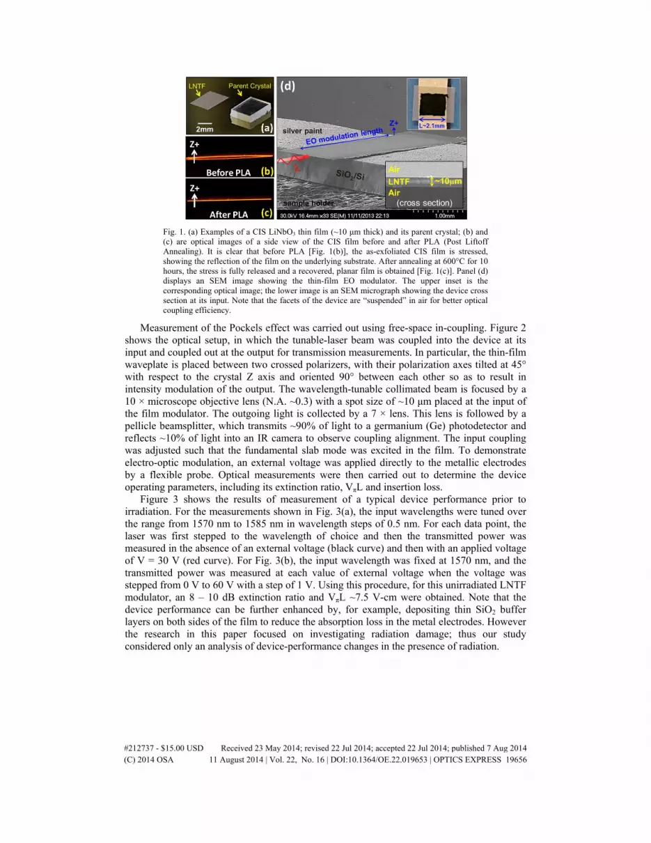
Fig. 1. (a) Examples of a CIS LiNbO3 thin film (~10 m thick) and its parent crystal; (b) and
(c) are optical images of a side view of the CIS film before and after PLA (Post Liftoff
Annealing). It is clear that before PLA [Fig. 1(b)], the as-exfoliated CIS film is stressed,
showing the reflection of the film on the underlying substrate. After annealing at 600°C for 10
hours, the stress is fully released and a recovered, planar film is obtained [Fig. 1(c)]. Panel (d)
displays an SEM image showing the thin-film EO modulator. The upper inset is the
corresponding optical image; the lower image is an SEM micrograph showing the device cross
section at its input. Note that the facets of the device are “suspended” in air for better optical
coupling efficiency.
Measurement of the Pockels effect was carried out using free-space in-coupling. Figure 2
shows the optical setup, in which the tunable-laser beam was coupled into the device at its
input and coupled out at the output for transmission measurements. In particular, the thin-film
waveplate is placed between two crossed polarizers, with their polarization axes tilted at 45°
with respect to the crystal Z axis and oriented 90° between each other so as to result in
intensity modulation of the output. The wavelength-tunable collimated beam is focused by a
10 × microscope objective lens (N.A. ~0.3) with a spot size of ~10 m placed at the input of
the film modulator. The outgoing light is collected by a 7 × lens. This lens is followed by a
pellicle beamsplitter, which transmits ~90% of light to a germanium (Ge) photodetector and
reflects ~10% of light into an IR camera to observe coupling alignment. The input coupling
was adjusted such that the fundamental slab mode was excited in the film. To demonstrate
electro-optic modulation, an external voltage was applied directly to the metallic electrodes
by a flexible probe. Optical measurements were then carried out to determine the device
operating parameters, including its extinction ratio, VπL and insertion loss.
Figure 3 shows the results of measurement of a typical device performance prior to
irradiation. For the measurements shown in Fig. 3(a), the input wavelengths were tuned over
the range from 1570 nm to 1585 nm in wavelength steps of 0.5 nm. For each data point, the
laser was first stepped to the wavelength of choice and then the transmitted power was
measured in the absence of an external voltage (black curve) and then with an applied voltage
of V = 30 V (red curve). For Fig. 3(b), the input wavelength was fixed at 1570 nm, and the
transmitted power was measured at each value of external voltage when the voltage was
stepped from 0 V to 60 V with a step of 1 V. Using this procedure, for this unirradiated LNTF
modulator, an 8 – 10 dB extinction ratio and VπL ~7.5 V-cm were obtained. Note that the
device performance can be further enhanced by, for example, depositing thin SiO2 buffer
layers on both sides of the film to reduce the absorption loss in the metal electrodes. However
the research in this paper focused on investigating radiation damage; thus our study
considered only an analysis of device-performance changes in the presence of radiation.
#212737 - $15.00 USD Received 23 May 2014; revised 22 Jul 2014; accepted 22 Jul 2014; published 7 Aug 2014
(C) 2014 OSA 11 August 2014 | Vol. 22, No. 16 | DOI:10.1364/OE.22.019653 | OPTICS EXPRESS 19656
Fig. 2. Schematic of the experimental setup for free-space coupling. The collimated beam is
focused by a 10 × objective lens to achieve a spot size of ~10 m at the device input. The
outgoing light is then collected by another 7 × lens. A pellicle beamsplitter was used so that
~10% of light is reflected to an IR camera for the observation of coupling while ~90% of light
is transmitted to the photodetector. The electro-optic measurement is performed by applying an
external voltage directly to the top electrode of the film. P: polarizer; f: lens; PD:
photodetector.
Fig. 3. (a) and (b) display examples of the electro-optic modulation using virgin LNTF: a ~10
dB extinction ratio (modulation depth of ~90%) with ~7.5 V-cm VπL parameters were
measured (see text for a description of the measurement protocol). A sine-squared function
was used for the data fitting (solid lines). The device overall length is ~3.5 mm, with an
effective electrode length of ~2.1 mm.
The CIS-film (~10 m) modulators were subsequently irradiated by He+ at different
energies and doses to study the effect of radiation on modulator performance. For
convenience, irradiation was performed under the same conditions as for implantation of bulk
materials for slicing. Note that to ensure homogeneous irradiation, the beam current during
the implant was maintained at ~280 ± 10 nA/cm2. Two energies were chosen: 2.3 MeV and
3.6 MeV. From SRIM (Stopping and Range of Ions in Matter) [18] calculations, the stopping
ranges of 2.3 and 3.6 MeV He+ are ~5 m (in the middle of the film) and ~9 m below the top
surface, with straggle distances of ~300 nm and ~400 nm, respectively. After irradiation, the
device performance was then tested again and compared that of the unirradiated modulator.
Also note that to alleviate any possibility of heating during irradiation, thus giving rise to
electrode damage, the irradiation performed in our experiments was raster-scanned under
water-cooled environment.
Figure 4 show the modulator appearance and performance after irradiation. Figures 4(a)
and 4(b) are optical images of the thin-film modulators after 3.6 MeV He+ irradiation at doses
of 1 × 1016 cm2 and 5 × 1016 cm2, respectively. Earlier work [17] had shown that this form
of He+ irradiation gives rise to a strained thin film. In addition, in our experiments, after a
bombardment dose of 5 × 1016 cm2 He+, this built-in stress is sufficiently high, in some cases,
that the film partially cracks. Figures 4(c) and 4(d) display the modulator output signal for
three values of irradiation when different input wavelengths [Fig. 4(c)] and voltages [Fig.
4(d)] are used. The inset in Fig. 4(c) shows the normalized transmitted power for each
irradiation case. The performance degrades as the dose is increased. For example, our initial
#212737 - $15.00 USD Received 23 May 2014; revised 22 Jul 2014; accepted 22 Jul 2014; published 7 Aug 2014
(C) 2014 OSA 11 August 2014 | Vol. 22, No. 16 | DOI:10.1364/OE.22.019653 | OPTICS EXPRESS 19657

experiments showed that a He+-2 × 1016 cm1-dose irradiation led to an additional waveguide
loss of ~9 dB, a ~5 dB lower extinction ratio, and a ~73% degraded VπL value for the
modulator.
A careful consideration of results, such as in Figs. 4, 5, and Table 1 described below,
shows that in our study, there are two sources of modulator damage. The first is crystal
(lattice) damage from the He ion-beam interactions. This damage leads to the formation of
point defects, dislocations, and related extended defects, all of which increase optical
scattering [19]. In addition, during implantation at doses of > 0.5 × 1016 cm2, ~5 nm He
bubbles self-assemble in the solid lattice within the stopping region [20]. In the presence of
higher-temperature annealing, such as the T = 600°C annealing process used here, larger-
scale ~100 nm He bubbles are formed from the coalescence of the nascent 5 nm bubbles,
which have a significant Rayleigh optical scattering cross section [21]. Note that without
proper post-irradiation annealing, the presence of these defects and the associated lattice
disorder can shift the refractive index profile of the guide and hence induce changes in the
modal profiles, resulting in leaky modes [22]. Such altered modal structures manifest
themselves in part as light scattered away from the guiding region.
To illustrate the role of this scattering, a 633-nm-wavelength probe was used for the
observation of visible scattered light in the waveguide and observed through the top surface
of the film. In the presence of 3.6 MeV He+ irradiation to a dose of 2 × 1016 cm2, strong light
scattering through the top surface of the thin-film modulator is seen; see Figs. 5(a) and 5(b).
Fig. 4. Panels (a) and (b) are optical images of the modulators after 3.6 MeV He+ irradiation at
a dose of 1016 cm2. It is clear that the film is strained and, when the dose is 5 × 1016 cm2,
the stress is large enough to result in film fracture. Panels (c) and (d) are measured data
showing that as the dose is increased, device performance degrades, viz a ~9 dB additional
waveguide loss, ~5 dB lower extinction ratio and a ~73% increased VπL value indicating
degradation for a dose of 2 × 1016 cm2. The inset in Fig. 4(c) shows the degradation of the
extinction ratio using the normalized transmitted power for each irradiated condition, where
Pnorm is the normalized transmitted power. Figure 4(e) and the inset show a 2.3 MeV He+
irradiated case at a dose of 1 × 1016 cm2. Compared with 3.6 MeV He+ with the same
irradiation dose [i.e. 1 × 1016 cm2, blue curve in panel (c)], additional ~5.5 dB propagation
loss is observed for 2.3 MeV He+ irradiation, due to higher overlap of the damaged region (in
the center) and the optical guided mode.
In addition, this scattering also increases the device propagation loss over that of the
unirradiated device. For example, measurements of the loss in transmission show that it
increases from ~2 dB in the implanted device to ~7.5 dB for a dose of 1 × 1016 cm2, to ~11.3
dB for a dose of 2 × 1016 cm2, and to ~16 dB for a dose of 5 × 1016 cm2 at a beam energy of
#212737 - $15.00 USD Received 23 May 2014; revised 22 Jul 2014; accepted 22 Jul 2014; published 7 Aug 2014
(C) 2014 OSA 11 August 2014 | Vol. 22, No. 16 | DOI:10.1364/OE.22.019653 | OPTICS EXPRESS 19658
3.6 MeV. In addition, our experiments showed that, in comparison with 3.6 MeV He+
irradiation, 2.3 MeV irradiation for the same dose yields higher propagation loss (see Fig.
4(e) where an additional propagation loss of ~5.5 dB was observed). This result is attributed
to the energy-dependent depth of damage, which results in the spatial overlap between the
optical guided mode and the He+-damaged region, since the 2.3 MeV He+ ions stop in the
center of the film, while 3.6 MeV He+ ions stop at the bottom. Thus when a Gaussian beam is
coupled into the center of the film, the higher overlap leads to stronger light scattering from
the damaged region for the 2.3 MeV case, therefore resulting in greater loss in the guided
mode.
The second source of modulator degradation is the material birefringence change caused
by irradiation. This change can be attributed to both an increase in strain within the crystal
and a partial loss of crystallinity in the stopping region. Strain is induced in the crystal during
He+ irradiation, due to the presence of interstitial He, nm-scale nascent clusters of He, or
through the formation of larger bubbles [21]. This strain can lead to a significant change in
the crystal birefringence following ion irradiation. In addition, He+ irradiation is also known
via optical and electrical microscopy [20] to generate a thin region with partially degraded
crystallinity. Such a region will also have a different (lower) birefringence than the
unirradiated crystal.
In order to examine the effects of this birefringence, measurements were made of the
polarization response as a function of the input wavelength for unirradiated and irradiated
films. Again, two ion energies were used. The results of this measurement are illustrated
using the data in Fig. 4(c), where it is seen that after irradiation, a change occurs in the phase
of the modulation envelope and a decrease in the dependence of the output power on
wavelength. In addition, the depth of modulation (or extinction ratio) is substantially reduced
and that higher dose increases the reduction in modulation depth; see the inset in Fig. 4(c).
Figure 4(d) shows voltage-dependent modulation measurements at a wavelength of = 1570
nm; again notice that higher dose degrades the modulation depth. This degradation in the
modulation is consistent with an irradiation-induced decrease in the intrinsic birefringence.
Note that although the use of 2.3 MeV He+ results in higher overlap with the optical mode,
the measured VπL (~9.5 V-cm) is still comparable in magnitude to the value after 3.6 MeV
He+ irradiation (~10 V-cm) for the same dose (1 × 1016 cm2). Considering that electro-optic
polarization is directly related to Raman susceptibility [23, 24], a micro-Raman edge scan at
different depths was performed to resolve any irradiation-induced change in the active
phonon modes [11]. The results (not presented here) show that these two energies, both
having comparable straggle length with the thickness of the film, give rise to similar
distributions of the built-in strain field (obtained from spectral shift) and crystalline damage
(from linewidth broadening). Such comparable damage profiles indicate the two cases having
similar overall changes of birefringence (discussed below) and EO coefficients (r33 and r31).
Thus, for these two cases, the voltage-dependent retardation would result in similar values of
VπL.
The irradiation-induced change in the intrinsic film birefringence can be further
characterized using a quantity based on a measurement of the normalized birefringence of the
LNTF modulator. In particular, it is known [25] that the phase retardation of polarized light
propagating through a waveplate (birefringent material) is proportional to its index anisotropy
or birefringence; this basic phenomenon allows us to measure this same quantity in our LNTF
modulator using a measurement of the extinction ratio. Thus a sine-squared
function 2 ( )sin [ ]o e
o
L n n
, corresponding to the power transmittance of the system, was used
to fit the measured normalized wavelength-dependent modulation and, hence, the change of
the index anisotropy for the two indices ( )o en n induced by irradiation. Note that prior to
irradiation, the LNTF sample had ( )o en n equal to ~ 0.078, which agrees well with the
#212737 - $15.00 USD Received 23 May 2014; revised 22 Jul 2014; accepted 22 Jul 2014; published 7 Aug 2014
(C) 2014 OSA 11 August 2014 | Vol. 22, No. 16 | DOI:10.1364/OE.22.019653 | OPTICS EXPRESS 19659

theoretical value (~ 0.074) using the Sellmeier equation for = 1570 nm [9]. After He+
irradiation with a dose of 2 × 1016 cm2, the difference ' '( )o en n decreased to ~ 0.053. As the
irradiation dose is increased, greater lattice distortion occurs due to an increase in the induced
stress and defect clusters [10] such that the birefringence or anisotropy is decreased. Defining
an isotropy factor (C), ' '( ) ( )'
( )
o e o e
o e
n n n nn nC
n n n
, we can find the degree of change of
the anisotropy/birefringence. For example, C ~ 0.32 for our 2 × 1016 cm2 He+ fluence. This
result indicates that, in the range of the wavelengths used in the experiments (telecom
windows), ~ 68% of the material birefringence is preserved. Note that an optically isotropic
material ( ' 'e on n ) will have a 1C , and for our unirradiated LNTF, 0 ( ' ).C n n Also
before post-liftoff annealing, e.g. as shown in Fig. 1(b), high residual stress and radiation
defects from 5 × 1016 cm2 He+ irradiation and the exfoliation process leads to a change in
birefringence yielding a ~ 0.5C [17]. The estimated error of ~ 2% originates from
uncertainty in measurement of the propagation length ΔL. In general, higher-dose irradiation
results in greater change of anisotropy/birefringence, and the calculated C factor. The analysis
is summarized in Fig. 5(c).
Fig. 5. (a) and (b): optical top-surface images of end-facet-coupled light using a visible (red)
light source to directly observe scattering. (a): light coupled into an unirradiated LNTF sample;
(b) light coupled into an irradiated thin film (2.3 MeV He+ to a dose of 2 × 1016 cm2). In (b),
the scattered light through the top surface of a thin-film modulator is readily seen (designated
by a yellow arrow. See text for a discussion of the origin of the scattering. (c): The change of
LNTF index anisotropy/birefringence under different conditions (wavelength ~1570 nm).
PLA stands for Post Liftoff Annealing; see Figs. 1(b) and 1(c) for the corresponding optical
images. After PLA, the thin-film modulator is irradiated with 3.6 MeV He+ with different
doses. It is clear that as the irradiation dose is increased, the damage of lattice structure is
enhanced such that the change of anisotropy (C factor) is greater. Note that if the material is
optically-isotropic, C = 1.
Several groups [26–28] have reported measurements of the index profile from He+
implantation in bulk LiNbO3 waveguides. These measurements show that for high-dose He+
irradiation (>1016 cm2), irradiation-induced lattice damage and strain give rise to a percent-
level decrease in both no and ne in the nuclear damage region. This phenomenon is
sufficiently reproducible that it has been used to form an optical barrier for the confinement
of guided light in high-quality optical waveguides [29]. Our measurements using thin films (C
~0.32 with = 1570 nm) show that under the similar implantation parameters, the preserved
birefringence agrees well with literature values [26–28], if the appropriate wavelength
dispersion is taken account (for example, in [28], C ~ 0.45 using second harmonic signals of
= 1060 nm). The near coincidence of the change of birefringence in the ~10 m-thick thin
film and ~ 500 m-thick bulk LiNbO3 crystal is attributed to the fact that such index effects
result from local structural changes and the induced stress fields, both of which are of
#212737 - $15.00 USD Received 23 May 2014; revised 22 Jul 2014; accepted 22 Jul 2014; published 7 Aug 2014
(C) 2014 OSA 11 August 2014 | Vol. 22, No. 16 | DOI:10.1364/OE.22.019653 | OPTICS EXPRESS 19660

comparable magnitude in thicker samples. Note that since the stopping cross section scales
with the projectile atomic number (Z) [30], radiation damage is expected to be greater if
heavy-ion irradiation is used.
Finally, Table 1 summarizes the results of our measurements of He+-irradiation damage in
our LiNbO3 thin-film EO modulators and the corresponding damage mechanisms to the
device operating parameters. The reduced extinction ratio and the increased VπL are also
compared in the table to the values measured in the unirradiated case. It is clear from this
table that both the total dose and the distribution of that dose with respect to the waveguide
optical mode determine the degradation in extinction ratio, VπL, and insertion loss in the
presence of ionizing radiation, viz He+.
Table 1. Summary of Device Parameters in the Absence and Presence of Different
Irradiation Conditions and Examples of the Corresponding Damage Mechanisms
Thin Film (~10 µm thick)
Prototype 2.3 MeV 3.6 MeV He
+ dose (cm
-2)
Damage Mechanism 1 × 10
16 1 × 10
16 2 × 10
16 5 × 10
16
Extinction Ratio (dB)
~8 – 10 ~6.5 dB lowered
~4 dB lowered
~5 dB lowered
~6.2 dB lowered
1. Lattice disorder (strain) 2. Light scattering from interstitials
VπL (V-cm) ~7.5 ~9.5
(~27%) ~10
(~33%) ~13
(~73%) N.A.*
1. Lattice disorder 2. Electrodes damage
Insertion Loss (dB)
~2 ~13 ~7.5 ~11.3 ~16 1. Absorption 2. Damage at interface 3. Light scattering
*films are partially cracked
3. Conclusions
In conclusion, He+-induced radiation damage in 10- m-thick LNTF modulators is
investigated. Our results show that lattice disorder and stress give rise to the degradation of
device performance for a dose 1016 cm2. The device performance, determined primarily by
operating parameters, including extinction ratio, VπL, and insertion loss, has a complex
dependence on the energy and dose of the He+ radiation. Two He+ energies, corresponding to
different stopping ranges, were used and measurements of films irradiated using these
energies demonstrate that the degree of overlap between guided modes with damaged regions
has a significant effect on the degree of achievable modulation. In particular, the less
energetic He+ ions at 2.3 MeV yielded significant insertion loss degradation than that from the
more energetic 3.8 MeV He+ ions due to the overlap of the stopping range with the waveguide
mode. For a given or fixed ion energy, the degradation in operating parameters increased as
the ion dose was increased. In addition, the device performance is influenced by scattering
from interstitial damage states and irradiation-induced strain, further altering the optical
anisotropy and the EO coefficients. Finally, note that, given the results of our research, it may
be possible to redesign an electro-optical structure so as to make it sensitive to radiation
damage. For example, the device modal structure could be reworked so as to make radiation
alteration of the mode by ion bombardment a sensitive optical-detection scheme. The
fundamental knowledge measured here can provide the information needed to design such a
new instrument.
Acknowledgments
This work was supported by the Department of the Defense, Defense Threat Reduction
Agency (DTRA) under HDTRA1-11-1-0022, and the National Science Foundation (NSF)
under Award Number ECCS-1302488.
#212737 - $15.00 USD Received 23 May 2014; revised 22 Jul 2014; accepted 22 Jul 2014; published 7 Aug 2014
(C) 2014 OSA 11 August 2014 | Vol. 22, No. 16 | DOI:10.1364/OE.22.019653 | OPTICS EXPRESS 19661