Electro-Optical Na0.5K0.5NbO3 Films - DiVA-Portal
119
Electro-Optical Na 0.5 K 0.5 NbO 3 Films MATS BLOMQVIST Doctoral Thesis Stockholm, Sweden 2005
-
Upload
khangminh22 -
Category
Documents
-
view
2 -
download
0
Transcript of Electro-Optical Na0.5K0.5NbO3 Films - DiVA-Portal
Electro-Optical Na0.5K0.5NbO3 Films
MATS BLOMQVIST
Doctoral Thesis
Stockholm, Sweden 2005

Typeset in LATEX.
Cover picture: Dark line spectra in TE and TM polarized light showing waveguidepropagation modes for a 0.9 µm Na0.5K0.5NbO3 film waveguide on sapphire (Al2O3)substrate at three wavelengths.
TRITA FYS 5299ISSN 0280-316XISRN KTH/FYS/FTS/R--05/5299--SEISBN 91-7178-007-6
KTH FysikSE-100 44 Stockholm
SWEDEN
Akademisk avhandling som med tillstånd av Kungl Tekniska högskolan framläggestill offentlig granskning för avläggande av Teknologie doktorsexamen fredagen den20 maj 2005 i D1, Kungl Tekniska högskolan, Lindstedtsvägen 17, 2tr, Stockholm.
c© Mats Blomqvist, maj 2005
Tryck: Universitetsservice US AB

iii
Abstract
Ferroelectric oxides are a group of advanced electronic materials witha wide variety of properties useful in applications such as memory devices,resonators and filters, infrared sensors, microelectromechanical systems, andoptical waveguides and modulators.
Among the oxide perovskite-structured ferroelectric thin film materials,sodium potassium niobate or Na0.5K0.5NbO3 (NKN) has recently emerged asone of the most promising materials in radio frequency (rf) and microwaveapplications due to high dielectric tunability and low dielectric loss.
This thesis presents results on growth and structural, optical, and electri-cal characterization of NKN thin films. The films were deposited by rf-mag-netron sputtering of a stoichiometric, high density, ceramic Na0.5K0.5NbO3
target onto single crystal LaAlO3 (LAO), Al2O3 (sapphire), SrTiO3, andNd:YAlO3, and polycrystalline Pt80Ir20 substrates. By x-ray diffractometry,NKN films on c-axis oriented LaAlO3, SrTiO3 and Nd:YAlO3 substrates werefound to grow epitaxially, whereas films on r-cut sapphire and polycrystallinePt80Ir20 substrates were found to be preferentially (00l) oriented. The surfacemorphology was explored using atomic force microscopy.
Optical and waveguiding properties of the Na0.5K0.5NbO3/substrate het-erostructures were characterized using prism-coupling technique. Sharp anddistinguishable transverse magnetic and electric propagation modes were ob-served for NKN thicknesses up to 2.0 µm. The extraordinary and ordinaryrefractive indices were calculated together with the birefringence of the NKNmaterial. The electro-optic effect in transverse geometry was measured intransmission, where the effective linear electro-optic response was determinedto reff = 28 pm/V for NKN/Al2O3 with an applied dc field up to 18 kV/cm.
The ferroelectric state in NKN films on Pt80Ir20 at room temperaturewas indicated by a polarization loop with saturated polarization as high as33.4 µC/cm2 at 700 kV/cm, remnant polarization of 10 µC/cm2, and coercivefield of 90 kV/cm. Current-voltage characteristics of vertical Au/NKN/PtIrcapacitive cells and planar Au/NKN/LAO interdigital capacitors (IDCs) show-ed very good insulating properties, with the leakage current density for anNKN IDC on the order of 30 nA/cm2 at 400 kV/cm. Rf dielectric spec-troscopy demonstrated low loss, low frequency dispersion, and high voltagetunability. At 1 MHz, NKN/LAO showed a dissipation factor tan δ = 0.010
and a tunability of 16.5% at 200 kV/cm. For the same structure the frequencydispersion was ∆εr = 8.5% between 1 kHz and 1 MHz.
Key words: ferroelectrics, sodium potassium niobates, thin films, rf-magne-tron sputtering, waveguiding, refractive index, prism-coupling, electro-opticeffects, dielectric tunability

iv
Sammanfattning
Ferroelektriska oxider tillhör en grupp avancerade elektroniska materialmed en stor blandning av egenskaper som gör dem attraktiva i tillämpningar,såsom datorminnen, resonatorer och filter, infraröda sensorer, mikroelektro-mekaniska system, samt optiska vågledare och modulatorer.
Bland ferroelektriska tunnfilmsmaterial med perovskitstruktur har nat-rium-kalium-niobat eller Na0.5K0.5NbO3 (NKN) nyligen trätt fram som ettav de mest lovande materialen för radiofrekvens- och mikrovågstillämpningartack vare hög dielektrisk avstämbarhet och låga dielektriska förluster.
Den här avhandlingen presenterar resultat runt framställning och struktu-rell, optisk och elektrisk karakterisering NKN-tunnfilmer. Tunnfilmerna till-verkades med rf-magnetronsputtring av en stökiometrisk Na0.5K0.5NbO3 ke-ram av hög densitet på olika enkristallina (LaAlO3 (LAO), Al2O3, SrTiO3
och Nd:YAlO3) och polykristallina (Pt80Ir20) substrat. Röntgendiffraktion an-vändes för att bestämma filmernas kristallstruktur och ordning. Filmytornasjämnhet mättes med hjälp av atomkraftsmikroskopi.
Optiska och vågledande egenskaper hos Na0.5K0.5NbO3/substrat-hetero-strukturerna undersöktes med en prism-kopplingsteknik. Skarpa, urskiljbaratransversella magnetiska och elektriska moder observerades. Det ordinära ochextraordinära brytningsindexen beräknades, så även materialets dubbelbryt-ning. Den elektrooptiska effekten i en transversell geometri mättes i trans-mission, där den effektiva linjära elektrooptiska koefficienten bestämdes tillreff = 28 pm/V för NKN på Al2O3 med elektriskt dc fält upp till 18 kV/cm.
Att NKN är i ett ferroelektriskt tillstånd vid rumstemperatur visades meden polarisationkurva. Ström-spänningskarakteristik av en NKN kondensator-struktur indikerade mycket god isolerande förmåga. Rf-spektroskopi demon-strerade låga förluster, låg frekvensdispersion och hög avstämbarhet.
Nyckelord: ferroelektrika, natrium-kalium-niobater, tunnfilmer, rf-magne-tronsputtring, vågledning, brytningsidex, prism-kopplingsteknik, elektroop-tisk effekt, dielektrisk avstämbarhet
v
Preface
This thesis is based on my work carried out as a Ph.D. student between September2000 and May 2005 at the Department of Condensed Matter Physics, Laboratory ofSolid State Devices, IMIT, Royal Institute of Technology, Stockholm-Kista, Sweden.The research has all through been supported by an Agilent Technologies Ph.D.Fellowship award.
List of publications
The following publications and manuscripts are included in the thesis:
I. High-performance epitaxial Na0.5K0.5NbO3 thin films by magnetron sputteringM. Blomqvist, J.-H. Koh, S. Khartsev, A. Grishin, and J. Andréasson,Appl. Phys. Lett., 81, 337 (2002).
II. Rf-magnetron sputtered ferroelectric (Na,K)NbO3
M. Blomqvist, J.-H. Koh, S. Khartsev, and A. Grishin,Proceedings of the 13th IEEE International Symposium on Applications ofFerroelectrics, 195 (2002).
III. Optical waveguiding in magnetron-sputtered Na0.5K0.5NbO3 thin films on sap-phire substratesM. Blomqvist, S. Khartsev, A. Grishin, A. Petraru, and Ch. Buchal,Appl. Phys. Lett., 82, 439 (2003).
IV. Rf sputtered Na0.5K0.5NbO3 films on oxide substrates as optical waveguidingmaterialM. Blomqvist, S. Khartsev, A. Grishin, and A. Petraru,Integr. Ferroelectr., 54, 631 (2003).
V. Visible and IR light waveguiding in ferroelectric Na0.5K0.5NbO3 thin filmsM. Blomqvist, S. Khartsev, and A. Grishin,Integr. Ferroelectr., 69, 277 (2005).
VI. Electro-optic ferroelectric Na0.5K0.5NbO3 filmsM. Blomqvist, S. Khartsev, and A. Grishin,To appear in IEEE Photon. Technol. Lett. (2005).
VII. Electro-optic effect in ferroelectric Na0.5K0.5NbO3 thin films on oxide sub-stratesM. Blomqvist, S. Khartsev, and A. Grishin,Submitted to Integr. Ferroelectr. (2005).
The following publications were not included in the thesis since they are on othersubjects.

vi
VIII. On-wafer continuous-wave operation of InGaN/GaN violet laser diodesG. Hasnain, T. Takeuchi, R. Schneider, S. Song, R. Twist, M. Blomqvist,C. Kocot, and C. Flory,Electronics Letters, 36, 1779 (2000).
IX. GaN-based light emitting diodes with tunnel junctionsT. Takeuchi, G. Hasnain, S. Corzine, M. Hueschen, R. Schneider, C. Kocot,M. Blomqvist, Y.-L. Chang, D. Lefforge, M. Krames, L. Cook, and S. Stock-man,Jpn. J. Appl. Phys., 40, L861 (2001).
X. The effect of carbon and germanium on phase transformation of nickel onSi1−x−yGexCy epitaxial layersJ. Hållstedt, M. Blomqvist, P. O. Å. Persson, L. Hultman, and H. H.Radamson,J. Appl. Phys., 95, 2397 (2004).
Comments on my participation
Throughout the publications the thin films were prepared by S. Khartsev. In pa-per I, the Na0.5K0.5NbO3 target was prepared in cooperation with Luleå University.J.-H. Koh helped with thin film processing and the electrical characterization in pa-pers I and II. The results in publication II were presented orally at the InternationalJoint Conference on the Applications of Ferroelectrics 2002 (IFFF 2002) in Nara,Japan, May 2002. Papers III and IV are the result of collaboration with Prof. Ch.Buchal’s group at the research center in Jülich, Germany, where I performed theprism-coupling measurements together with A. Petraru and S. Kahl. The resultsin paper IV were presented orally at the 15th International Symposium on Inte-grated Ferroelectrics (ISIF 2003) in Colorado Springs, CO, USA, March 2003. Thewaveguiding properties in publication V and manuscript VI were studied at Agi-lent Laboratories, Palo Alto, CA, USA. J.-H. Kim assisted with AFM imaging inpaper V. Paper V was presented as a poster at the 16th International Symposiumon Integrated Ferroelectrics (ISIF 2004) in Gyeongju, South Korea, April 2004, andmanuscript VII was presented with a poster at the 17th International Symposiumon Integrated Ferroelectrics (ISIF 2005) in Shanghai, China, April 2005.
Except for the contributions mentioned above, I made all the measurementsand calculations, and I wrote all the manuscripts. My supervisor, Prof. A. Grishin,and our senior scientist S. Khartsev, have both throughout this thesis work beeninvolved in experimental and theoretical discussions.
During my research I have been supported by an Agilent Technologies Ph.D.Fellowship award through their University Relations Ph.D. Fellowship program andmy mentor at Agilent has been Dr. W. Ishak.
vii
Acknowledgements
Many persons have in different ways been helping and supporting me throughoutthis work.
First, I would like to thank my supervisor, Prof. Alex Grishin, for giving mesupport, and being an inspiring and encouraging academic advisor.
I would like to acknowledge all former and present the people in our depart-ment of Condensed Matter Physics; Dr. Sergey Khartsev for his tremendous workin helping me with the experiments and for his critical comments, Dr. Sören Kahl,my room mate this final year, for our collaboration on optical measurements, in-teresting and fruitful discussions, and friendship, Dr. Jung-Hyuk Koh for sharingoffice space and introducing me to electrical characterization and lithography, Dr.Peter Johnsson for all discussion on material science, as well as sports and politics,Rickard Fors for all vivid discussion on everything from Fermi surfaces to soccer,Beatriz Espinoza Arronte and Dr. Magnus Andersson for being lunch and coffee-break partners, Jang-Yong Kim for assistance in the clean room, Joo-Hyung Kimfor help with AFM measurements, and Jürgen, Vasyl, and Akira for help in variousways.
I would like to thank Dr. Henry Radamson and Julius Hållstedt for help anddiscussion on x-ray characterization. Also, thanks to Kestius Maknys and Dr.Srinivasan Anand for help with AFM imaging.
I wish to acknowledge Prof. Ch. Buchal and Dr. Adrian Petraru for friendlyhosting me and Sören during our stay in Jülich, and for introducing me to theprism-coupling technique.
I sincerely would like to express my gratitude to Dr. Waguih Ishak, Dr. KayGilles and Agilent Technologies for practically and financially supporting my re-search. Waguih, I am honored that you are attending my defense! I am also veryhappy that I came to meet all the people at Agilent Labs during my internship inthe fall of 2003, especially my supervisors Dr. Gerry Owen and Dr. Rick Trutna.Gerry, it was really a lot of fun working with you in the lab!
Also, I wish to thank all my friends outside my research environment for theirgood and developing company during my free time, whether it is on the golf course,on a steep slope in the Swedish mountains, or around a camp fire in the deep forrest.Especially, I am very happy for the support and friendship with you, Charlotte!
Finally, I wish to thank my caring family for their continuous support: Jan andElsa, Anders, Ingmar, Malin and Carl. It is great to know that at the end of theday you are always there for me.

viii
Symbols
c speed of lightc0 speed of light in vacuum (2.9979 · 108 m/s)C Curie-Weiss constantD electric displacementd piezoelectric coefficient tensorE electric fieldEc coercive electric fieldH magnetic fieldh film thicknessI light intensityk wave vectorM Jones matrixm mode numbern refractive indexne extraordinary refractive indexno ordinary refractive index∆n birefringence (ne − no)N effective refractive index of modesP electric polarizationPr remnant electric polarizationPs spontaneous electric polarizationQ dissipation factor, 1/tan δr electro-optic tensorrij electro-optic coefficientrc common linear electro-optic coefficientreff effective linear electro-optic coefficientR quadratic electro-optic coefficientS strainT mechanical stressT temperatureT0 Curie-Weiss temperatureTc Curie pointβ propagation constantΓ phase shiftε permittivity tensorεr relative permittivityε0 vacuum permittivity (8.8542 · 10−12 As/Vm)λ wavelengthµ0 vacuum permeability (4π · 10−7 Vs/Am)χ susceptibilityω angular frequency

ix
Abbreviations
AFM atomic force microscopyBTO barium titanate, BaTiO3
CCD charge-coupled deviceCVD chemical vapor depositionDRAM dynamic random access memoryEA electro-absorptionEO electro-opticFeFET ferroelectric field-effect transistorFeRAM ferroelectric random access memoryFWHM full width at half maximumHMDS hexamethyldisilazaneIDC interdigital capacitorKTN potassium tantalum niobate, KTaxNb1−xO3
LAO lanthanum aluminate, LaAlO3
LPE liquid-phase epitaxyMBE molecular-beam epitaxyMPB morphotropic phase boundaryMEMS microelectromechanical systemsNKN sodium potassium niobate, Na0.5K0.5NbO3
NLO nonlinear opticsOEIC optoelectronic integrated circuitPLD pulsed laser depositionPLZT lanthanum-modified lead zirconate titanate,
Pb1−xLax(Zry,Ti1−y)1−0.25xO3
PVD physical vapor depositionPZT lead zirconate titanate, Pb(Zrx,Ti1−x)O3
QWP quarter-wave platerms root mean squarerpm rotations per minuteSAW surface acoustic waveSBN strontium barium niobate, SrxBa1−xNb2O6
SHG second harmonic generationSPM scanning probe microscopySTO strontium titanate, SrTiO3
TE transverse electricTHG third harmonic generationTM transverse magneticVPE vapor-phase epitaxyXRD x-ray diffraction
Contents
Abstract . . . . . . . . . . . . . . . . . . . . . . . . . . . . . . . . . . . . . iii
Preface . . . . . . . . . . . . . . . . . . . . . . . . . . . . . . . . . . . . . v
List of publications . . . . . . . . . . . . . . . . . . . . . . . . . . . . . . . v
Comments on my participation . . . . . . . . . . . . . . . . . . . . . . . . vi
Acknowledgements . . . . . . . . . . . . . . . . . . . . . . . . . . . . . . . vii
Symbols . . . . . . . . . . . . . . . . . . . . . . . . . . . . . . . . . . . . . viii
Abbreviations . . . . . . . . . . . . . . . . . . . . . . . . . . . . . . . . . . ix
Contents x
1 Introduction 11.1 Thin Films in Optoelectronics . . . . . . . . . . . . . . . . . . . . . . 2
1.1.1 Optical modulators . . . . . . . . . . . . . . . . . . . . . . . . 21.1.2 Other waveguide applications . . . . . . . . . . . . . . . . . . 6
1.2 Outline . . . . . . . . . . . . . . . . . . . . . . . . . . . . . . . . . . 6
2 Ferroelectric Materials 72.1 Basic Physics . . . . . . . . . . . . . . . . . . . . . . . . . . . . . . . 7
2.1.1 History . . . . . . . . . . . . . . . . . . . . . . . . . . . . . . 82.1.2 Symmetry, piezo-, pyro-, and ferroelectricity . . . . . . . . . . 92.1.3 Ferroelectric domains and the hysteresis loop . . . . . . . . . 102.1.4 Ferroelectric Curie point and phase transitions . . . . . . . . 122.1.5 Antiferroelectricity . . . . . . . . . . . . . . . . . . . . . . . . 13
2.2 Optical and EO Properties of Ferroelectrics . . . . . . . . . . . . . . 132.2.1 Refractive index in ferroelectrics . . . . . . . . . . . . . . . . 142.2.2 Optical birefringence . . . . . . . . . . . . . . . . . . . . . . . 152.2.3 Electro-optic effect . . . . . . . . . . . . . . . . . . . . . . . . 172.2.4 Second harmonic generation . . . . . . . . . . . . . . . . . . . 192.2.5 Photo-elastic effect . . . . . . . . . . . . . . . . . . . . . . . . 202.2.6 Optical absorption . . . . . . . . . . . . . . . . . . . . . . . . 212.2.7 Optical scattering . . . . . . . . . . . . . . . . . . . . . . . . 21
x

xi
2.3 Materials . . . . . . . . . . . . . . . . . . . . . . . . . . . . . . . . . 222.3.1 Single crystals . . . . . . . . . . . . . . . . . . . . . . . . . . 222.3.2 Ceramics . . . . . . . . . . . . . . . . . . . . . . . . . . . . . 242.3.3 Thin films . . . . . . . . . . . . . . . . . . . . . . . . . . . . . 252.3.4 Perovskite-based materials . . . . . . . . . . . . . . . . . . . . 262.3.5 Na0.5K0.5NbO3 (NKN) . . . . . . . . . . . . . . . . . . . . . 302.3.6 Other corner sharing octahedra . . . . . . . . . . . . . . . . . 332.3.7 Organic polymers . . . . . . . . . . . . . . . . . . . . . . . . . 34
3 Growth Techniques and Processing 353.1 Rf-magnetron Sputtering . . . . . . . . . . . . . . . . . . . . . . . . 35
3.1.1 Sputtering process . . . . . . . . . . . . . . . . . . . . . . . . 363.1.2 Rf-sputtering . . . . . . . . . . . . . . . . . . . . . . . . . . . 363.1.3 Magnetron sputtering . . . . . . . . . . . . . . . . . . . . . . 37
3.2 Pulsed Laser Deposition, PLD . . . . . . . . . . . . . . . . . . . . . . 383.2.1 Description of the PLD system . . . . . . . . . . . . . . . . . 38
3.3 Na0.5K0.5NbO3 Target Preparation . . . . . . . . . . . . . . . . . . . 403.4 Processing of Na0.5K0.5NbO3 Films . . . . . . . . . . . . . . . . . . . 41
3.4.1 Lithography . . . . . . . . . . . . . . . . . . . . . . . . . . . . 413.4.2 Metallization . . . . . . . . . . . . . . . . . . . . . . . . . . . 433.4.3 Lift-off . . . . . . . . . . . . . . . . . . . . . . . . . . . . . . . 43
4 Characterization Techniques 454.1 Structural Characterization . . . . . . . . . . . . . . . . . . . . . . . 45
4.1.1 X-ray diffraction . . . . . . . . . . . . . . . . . . . . . . . . . 454.1.2 Atomic force microscopy . . . . . . . . . . . . . . . . . . . . . 524.1.3 Optical microscopy . . . . . . . . . . . . . . . . . . . . . . . . 534.1.4 Profilometry . . . . . . . . . . . . . . . . . . . . . . . . . . . 54
4.2 Electrical Characterization . . . . . . . . . . . . . . . . . . . . . . . . 554.2.1 P -E loop . . . . . . . . . . . . . . . . . . . . . . . . . . . . . 554.2.2 Dielectric spectroscopy . . . . . . . . . . . . . . . . . . . . . . 554.2.3 C-V characteristics . . . . . . . . . . . . . . . . . . . . . . . . 564.2.4 I-V characteristics . . . . . . . . . . . . . . . . . . . . . . . . 57
4.3 Optical Characterization . . . . . . . . . . . . . . . . . . . . . . . . . 574.3.1 Dielectric waveguides . . . . . . . . . . . . . . . . . . . . . . . 574.3.2 Prism-coupling . . . . . . . . . . . . . . . . . . . . . . . . . . 614.3.3 Electro-optical coefficients in transmission . . . . . . . . . . . 66
5 Summary of Results and Outlook 735.1 Structural and Electrical Properties of Na0.5K0.5NbO3 . . . . . . . . 73
5.1.1 Growth and crystallographic characteristics Na0.5K0.5NbO3
films . . . . . . . . . . . . . . . . . . . . . . . . . . . . . . . . 735.1.2 AFM characterization . . . . . . . . . . . . . . . . . . . . . . 745.1.3 Electrical characterization . . . . . . . . . . . . . . . . . . . . 74

xii CONTENTS
5.2 Optical and Waveguiding Properties of Na0.5K0.5NbO3 . . . . . . . . 755.3 Electro-optic Effect in Na0.5K0.5NbO3 . . . . . . . . . . . . . . . . . 755.4 Outlook . . . . . . . . . . . . . . . . . . . . . . . . . . . . . . . . . . 75
Bibliography 77
Papers 93

Chapter 1
Introduction
The development in microelectronics and optoelectronics over the past decades hasbeen remarkable, if not to say astonishing. The density of transistors in computerprocessors is still increasing according to Moore’s law1 and the speed of transmis-sion over optical fibers is growing rapidly. For this development to continue, newapproaches and new materials are needed.
Ferroelectric oxide materials possess several unique properties and are expectedto be of use in many fields:
• Ferroelectric thin films as high dielectric permittivity dielectrics in dynamicrandom access memories (DRAMs).
• Thin films in non-volatile ferroelectric random access memories (FeRAMs)and ferroelectric field-effect transistors (FeFETs), which make use of the non-linear hysteresis response of ferroelectrics.
• Ferroelectrics in integrated optical thin film modulators that explore theelectro-optic properties and high optical transparency of ferroelectric films.
• Ferroelectric films in transducers for converting electrical signals to mechani-cal responses and vice versa by using their piezoelectric properties.
• Thin films that make use of the pyroelectric effect for infrared (IR) detection.
• Ferroelectric thin films as high dielectric tunability and low dielectric lossmaterials at room temperature for microwave phase shifters, tunable filters,and varactors.
My main interests are the optical and electro-optical properties of a fairly newlydeveloped class of ferroelectric niobate thin films with potential applications inoptical communication.
1Moore’s law can be expressed for several different quantities and describes an exponentialgrowth over time of, for example, the number of memory cells per chip. Gordon Moore, one ofthe founders of Intel Corporation, formulated the law already in the 60s.
1

2 CHAPTER 1. INTRODUCTION
1.1 Thin Films in Optoelectronics
We encounter many optoelectronic devices in our daily life, for example self-lumi-nous displays, CD players, and various types of optical communication links. Withinthe area of fiber-optic communication, the focus is on photonic devices, which aremuch faster than their electronic counterparts. Very simplified, a fiber-optical linkconsists of a transmitter that generates light pulses through a semiconductor laserdiode, an optical fiber where the signal is propagating and amplified (e.g. throughan erbium-doped fiber amplifier), and finally an optical receiver that detects thelight pulses and converts them to electrical signals.
Thin films play a decisive role in optoelectronic integration, which is the combi-nation of electronic and optoelectronic devices into compact optoelectronic circuits.The integration can either be monolithic or hybrid. Monolithic integrated circuitswith electronic and optoelectronic devices are commonly referred to as optoelec-tronic integrated circuits or OEICs. A typical example of an OEIC is an optoelec-tronic transmitter and receiver consisting of a diode laser source, a light intensitymodulator, a light intensity detector, a multiplexer, a demultiplexer, and intercon-nection waveguides, on a single substrate. This OEIC has optical input/outputat one end and electrical input/output at the other end. Advantages with OEICsinclude a more compact, stable system working at high speeds, low power con-sumption, and potential cost reduction. Complications lie in the integration andmanufacturing, as will be discussed below.
In hybrid integration, different components are made using different substratesand then mounted together on a carrier. Generally, hybrid integration implies lowerchip manufacturing costs, but high chip mounting costs and problems with electricparasitics on the chip interconnects.
Thin films are used for most of the components in OEICs. In particular, ferro-electric films are of interest for optical modulator applications.
1.1.1 Optical modulators
The optical modulator is an important component of a fiber-optical system. An op-tical modulator can modulate the laser output light (intensity, frequency, phase orpolarization) at high speeds. Light modulation, which is the process of convertingdata (analog or digital) in electronic form to an optical signal, can be performed ei-ther by direct modulation of the laser or by external modulation through a modula-tor. Generally, external modulation is advantageous compared to direct modulationdue to low chirp and high speed. Also, intensity modulation is the most popularchoice for fiber-optic communication systems, primarily due to the simplicity ofenvelope photodetection [1]. Most of the modern wide-bandwidth modulators arebased on either of two types of physical effects; one is the linear electro-optic (EO)effect and the other is the electro-absorption (EA) effect. Both effects depend onthe applied electric field, which makes the modulators voltage-controlled devices.

1.1. THIN FILMS IN OPTOELECTRONICS 3
Figure 1.1 Conceptual drawing of a Mach-Zehnder waveguide modulator, fab-ricated with thin film technology on Si, here using BaTiO3 as the electro-opticmaterial. Until now, no such device has been completed [2].
Electro-optic modulation
Electro-optic modulation utilizes the electro-optic effect, which for an anisotropicelectro-optic material implies changes in the refractive indices with applied electricfield. The index change leads to a change in phase, which can be converted intointensity modulation in, e.g., a Mach-Zehnder interferometer.
Buchal et al. have described the physics of optical modulators and give exam-ples of different modulator concepts [2]. Commonly used today are transparent,bulk electro-optic crystals, such as LiNbO3 [3, 4]. These are obviously not suitedfor highly integrated OEICs, where the electro-optic material should be in thinfilm form on a common substrate. One of the most promising ideas is the use ofa ferroelectric thin film heterostructure in the form of an interferometric Mach-Zehnder waveguide modulator, as shown in Fig. 1.1. The ferroelectric material iselectro-optically active. If an electric field is applied across one of the arms in aMach-Zehnder modulator, a phase difference is introduced, and constructive or de-structive interference can be created on the output channel, as seen in Fig. 1.2. Twowaveguide modes with a phase difference of π rad/s couple into an antisymmetrichigher mode, which will not be sustained by a single-mode waveguide, but insteadwill be radiated to the substrate. Thus it is possible to modulate the light betweenon and off states by applying or not applying an electric field.

4 CHAPTER 1. INTRODUCTION
Figure 1.2 Illustration of constructive and destructive interference patterns in aMach-Zehnder waveguide modulator. Only if the outgoing waveguide is single mode,the resulting antisymmetric mode will be totally radiated into the substrate [2].
Developing a thin film heterostructure on semiconductor substrates, as the onein Fig. 1.1, is quite complicated. Due to the high indices of refraction for Si andGaAs, an oxide buffer layer of lower index is needed. This buffer layer shouldhave lower refractive index than the ferroelectric thin film, so that waveguiding willbe supported. In addition, this buffer layer must permit epitaxy,2 because deviceapplications of ferroelectric films require that properties similar to those found inbulk material will be maintained in deposited films. Promising results in recentpublications include SrTiO3 and MgO buffers on GaAs [5–7] and SrTiO3 bufferson Si [8].
Advantages with bulk EO modulators include very low optical losses, high powerhandling capability, broad bandwidth, and temperature insensitivity. Disadvan-tages are the large size, bias drifting, high driving voltages, polarization sensitivity,and complications in integration with other components. For thin films, the drivingvoltages would be lower and the size much reduced.
The main objective of my research is to synthesize and characterize ferroelectricsodium potassium niobate (Na0.5K0.5NbO3) thin films as an electro-optic waveguid-ing material in optical communication applications.
2Epitaxy implies growth of a single-phase film oriented according to the crystallographic struc-ture of the substrate, see Sect. 2.3.3.
1.1. THIN FILMS IN OPTOELECTRONICS 5
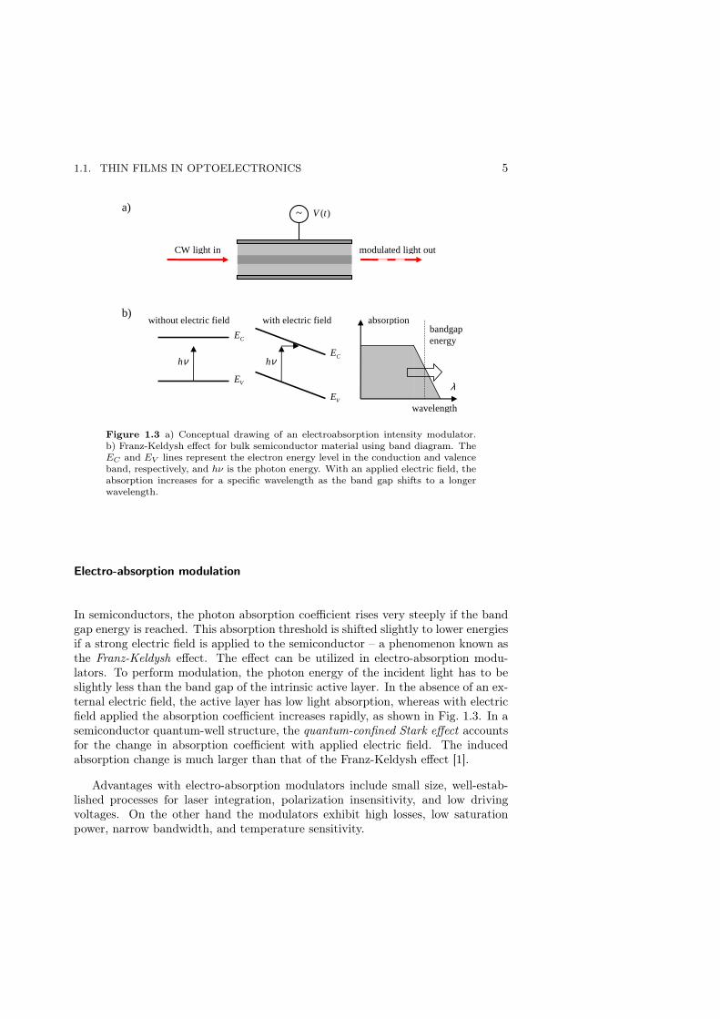
a)
b)
~ )(tV
CW light in modulated light out
νh
CE
VE
without electric field
νhCE
VE
with electric field absorption
λ
wavelength
bandgap energy
Figure 1.3 a) Conceptual drawing of an electroabsorption intensity modulator.b) Franz-Keldysh effect for bulk semiconductor material using band diagram. TheEC and EV lines represent the electron energy level in the conduction and valenceband, respectively, and hν is the photon energy. With an applied electric field, theabsorption increases for a specific wavelength as the band gap shifts to a longerwavelength.
Electro-absorption modulation
In semiconductors, the photon absorption coefficient rises very steeply if the bandgap energy is reached. This absorption threshold is shifted slightly to lower energiesif a strong electric field is applied to the semiconductor – a phenomenon known asthe Franz-Keldysh effect. The effect can be utilized in electro-absorption modu-lators. To perform modulation, the photon energy of the incident light has to beslightly less than the band gap of the intrinsic active layer. In the absence of an ex-ternal electric field, the active layer has low light absorption, whereas with electricfield applied the absorption coefficient increases rapidly, as shown in Fig. 1.3. In asemiconductor quantum-well structure, the quantum-confined Stark effect accountsfor the change in absorption coefficient with applied electric field. The inducedabsorption change is much larger than that of the Franz-Keldysh effect [1].
Advantages with electro-absorption modulators include small size, well-estab-lished processes for laser integration, polarization insensitivity, and low drivingvoltages. On the other hand the modulators exhibit high losses, low saturationpower, narrow bandwidth, and temperature sensitivity.

6 CHAPTER 1. INTRODUCTION
1.1.2 Other waveguide applications
Except for electro-optic modulators there are many other functional waveguide de-vices using ferroelectric thin films, such as directional couplers, optical wavelengthfilters, Bragg deflectors, and mode converters [9]. A specific branch of applica-tions utilize the acousto-optic effect in ferroelectrics. Surface acoustic wave (SAW)devices include mode converters, tunable wavelength filters, modulators and deflec-tors. Ferroelectrics often show strong second harmonic generation, see Sect. 2.2.4,which could be useful in wavelength converters for generation of shorter wavelengthlaser light [10,11].
1.2 Outline
This thesis contains five chapters, including this introduction. Chapt. 2 introducesthe ferroelectric materials. First basic physical properties are described, focusingon the optical and electro-optical effects. Then ferroelectric materials, interestingfor optical applications, are presented, paying special attention to the material,Na0.5K0.5NbO3, which has been the subject of my research. Chapt. 3 presents thetwo growth techniques that have been used to make our thin films, as well as a shortdescription of some processing techniques including lithography. Chapt. 4 describesthe structural, electrical, and optical characterization techniques that were used inthis work. Finally, the publications and manuscripts appended to this thesis aresummarized in Chapt. 5. This chapter also includes a short outlook for the future.

Chapter 2
Ferroelectric Materials
Ferroelectrics are a group of advanced electronic materials that possess a uniquemixture of dielectric, piezoelectric, pyroelectric, and electro-optic properties. Ferro-electric materials are often called functional or "intelligent" materials in the sensethat they can generate useful output to a simple input signal. For example, apiezoelectric material will generate an electric field with the input of stress, or viceversa.
In the future, smart ferroelectric materials in thin film form are expected tohave a considerable impact in a variety of areas such as memory devices (DRAMsand non-volatile FeRAMs) [12, 13], infrared (IR) sensors, optical waveguides andmodulators, resonators and filters, actuators and microelectromechanical systems(MEMS) [14]. This chapter will introduce the basic physics behind ferroelectricity,with main focus on optical properties. Furthermore, the most common ferroelectricmaterials will be introduced, addressing Na0.5K0.5NbO3 in more detail.
2.1 Basic Physics
Ferroelectric materials belong to the group of dielectric materials. If an electri-cal field is applied to a dielectric material, it will be electrically polarized. Thispolarization can be generated by one or more polarization mechanisms:
1. Electronic polarization which occurs due to distortion of the electron density.
2. Ionic polarization due to elastic deformation of ionic bond lengths or angles.
3. Orientational polarization due to changes in orientation of permanent dipolemoments.
4. Space charge polarization due to spatial separation of charges within thematerial.
The first three mechanisms are shown in Fig. 2.1. A sub-group of the dielectricmaterials show the property of spontaneous polarization. For these materials the
7

8 CHAPTER 2. FERROELECTRIC MATERIALS
Figure 2.1 Schematic description of electronic (A), ionic (B), and orientation (C)polarization [15].
centers of positive and negative charges do not coincide even without an appliedelectrical field. When the spontaneous polarization of a dielectric can be reversed byan electrical field of magnitude less than the dielectric breakdown of the material,it is called a ferroelectric material.
2.1.1 History
Ferroelectric crystals have been known for almost a century. The discovery waspreceded by the discovery of two related phenomena: piezoelectricity and pyroelec-tricity. Pyroelectricity was known since ancient times because of the ability of suchmaterials to attract objects when they are heated, and in 1880, Jacques and PierreCurie discovered the piezoelectric effect. In 1894, Pockels reported the anomalouslylarge piezoelectric constants of Rochelle salt (NaKC4H4O6·4H2O) [16]. The ferro-electricity of this salt was discovered in 1917 by A. M. Nicolson, J. A. Andersen,and W. G. Cady [17]. In 1920, Valasek observed the ferroelectric hysteresis loop ofthe crystal [18,19]. 15 years later, Busch and Scherrer discovered ferroelectricity inKH2PO4 and its sister crystals [20]. Now it was realized that ferroelectricity wasnot a property of some isolated materials, but rather a more common phenomenon.With the discovery of ferroelectricity in BaTiO3 (Wul and Goldman 1945, 1946) [21]a number of "firsts" were established: first ferroelectric without hydrogen bonds,

2.1. BASIC PHYSICS 9
first ferroelectric with more than one ferroelectric phase, and first ferroelectric witha paraelectric phase. In addition, the material was very stable and had a simple per-ovskite crystal structure, which facilitated the theoretical progress at microscopiclevel. In the 40s, 50s and 60s, many new ferroelectric materials were discovered,and the research focused on the most promising materials, such as the perovskiteand Tungsten Bronze structure oxides and ferroelectric polymers. With the im-proved thin film deposition techniques, attention has partly moved from ceramicsand single crystals to ferroelectric thin films.
The name ferroelectricity originates from the similarity of the fundamental con-cepts to those in ferromagnetic materials, such as magnetization, magnetic domains,and magnetic hysteresis loop. However, the physics behind these phenomena arecompletely different from those in ferroelectric materials. While magnetism can beunderstood as an intrinsically quantum mechanical phenomenon, ferroelectricity ingeneral may be described by means of classical physics.
2.1.2 Symmetry, piezo-, pyro-, and ferroelectricity
Structural symmetry affects physical properties of crystals, such as dielectric, elas-tic, piezoelectric, pyroelectric, ferroelectric, and nonlinear optical properties. De-pending on their geometry, crystals are commonly classified into seven systems.These systems can further be divided into point groups, so that the lattice struc-ture of all existing crystals can be described by 32 point groups. 21 of these groupsdo not possess any center of symmetry. All noncentrosymmetric point groups,except for the (432) point group, show piezoelectric effect along a unique axis di-rection [21–23].
Piezoelectricity is a phenomenon where positive and negative charges are gen-erated on the crystal surface when appropriate stresses are applied. The effect islinear, with reversal of the stimulus resulting in a reversal of the response. Theterm piezoelectricity (pressure electricity) was first suggested by W. Hankel in 1881and the effect is extensively used in applications [24,25].
Ten of the noncentrosymmetric groups have a unique polar axis. This impliesone unique rotation axis, and along this axis the atomic arrangement at one endis different from that at the other end. The crystals belonging to these groups arecalled polar crystals since they exhibit spontaneous polarization or, equivalently ex-pressed, electric moment per unit volume. Polar crystals exhibit the phenomenon ofpyroelectricity, which is a temperature dependence of the spontaneous polarization.As the temperature is changed, electric charges corresponding to the change of thespontaneous polarization appear on the surface of the crystal.
If the spontaneous polarization of a pyroelectric crystal can be reversed by anelectric field, it is called ferroelectric. Considering ferroelectrics as a subgroup ofthe pyroelectric class it follows that ferroelectric character cannot be determinedsolely from crystallographic characterization.

10 CHAPTER 2. FERROELECTRIC MATERIALS
2.1.3 Ferroelectric domains and the hysteresis loop
The physical quantity that describes the stored electric charge per unit area is calledthe electric displacement vector D and it is expressed as
D = Ps + εE + dT , (2.1)
where Ps is the spontaneous polarization, ε the dielectric tensor, E the electricfield, d the piezoelectric coefficient tensor and T the stress.
Most pyroelectric crystals exhibit spontaneous polarization in a certain tem-perature range and the direction of Ps can be reversed under the influence of anexternal electrical field, that is they are also ferroelectric crystals. From anotherstandpoint one can say that ferroelectric crystals are those crystals that have one ormore ferroelectric phases. The origin of spontaneous polarization is most easily un-derstood using an energy explanation. The total energy is a combination of dipoleinteraction energy, elastic energy, and entropy. It turns out that for ferroelectriccrystals, in specific temperature ranges, the energy minimum occurs for a polarizedcrystal (positive and negative ions are displaced).
Ferroelectric domains
In general, uniform alignment of electric dipoles only occurs in certain regions of acrystal. These regions are called ferroelectric domains and the boundary betweentwo domains is called the domain wall. The domain walls are typically thin (1-10lattice parameters across) and can be regarded as abrupt changes in the polariza-tion direction. Domain walls are characterized by the angle between the directionsof polarization on either side of the wall. Generally, domains are formed to reducethe energy of the system. The size and structure of the domains depend on manyfactors including the crystal symmetry, the electrical conductivity, the defect struc-ture, the magnitude of the spontaneous polarization, the grain size, as well as thesample geometry and the history of sample preparation. In strained epitaxial thinfilms, stable domain structures depend on substrate and film lattice parameters,differential thermal expansion coefficient between the film and substrate, coolingrate, and depolarizing fields and electrode geometry. Considering these dependen-cies, stable domain structures can be expressed in temperature-dependent stabilitymaps [26,27].
Ferroelectric domain structures can be revealed by various methods:
• Optical birefringence. Using a polarizing microscope to observe birefringenceinduced by mechanical stress or by an applied electric field [28,29].
• Second-harmonic generation. The intensity of the second-harmonic light de-pends on the optical interaction length within a single domain. Crossing adomain wall, the second-order non-linear coefficient changes sign and phasecancelation of the second harmonic occurs [30].

2.1. BASIC PHYSICS 11
Figure 2.2 A typical P -E hysteresis loop for a ferroelectric material [15].
• Electron microscopy. Using a scanning electron microscopy to observe thesurface of chemically etched samples [31,32].
• X-ray topography. Using x-rays to get a map of the crystal texture [33].
• Powder techniques. Applying the powder pattern method, where differentlycolored powders are carrying positive or negative charges. A mixture puton the ferroelectric will show a pattern depending on orientations of the do-mains [34,35].
• Liquid crystal method. Using liquid crystal displays, where the liquid-crystalmolecules align relative to the ferroelectric domains [36].
A just grown ferroelectric crystal always has a polydomain structure. This structurecan be transformed to a single domain structure by applying an external electricfield of high strength – a dynamic process called domain switching.
Ferroelectric hysteresis loop
A very important characteristic of ferroelectrics is the ferroelectric hysteresis loop,which means that for low field strengths, the polarization P is a double-valuedfunction of the applied electric field. A typical P -E hysteresis loop is given inFig. 2.2.

12 CHAPTER 2. FERROELECTRIC MATERIALS
-750 -500 -250 0 250 500 750-40
-30
-20
-10
0
10
20
30
40
Au/NKN/Pt80
Ir20
Pol
ariz
atio
n P
[µC
/cm
2 ]
Electric field E [kV/cm]
Figure 2.3 P -E hysteresis loop for a ferroelectric Au/NKN/PtIr vertical structure.
As the field strength increases from zero, the polarization increases until all thedomains are aligned in one direction (1 to 3). In this state of saturation the crystalis composed of single-oriented domains, and it has spontaneous polarization, whichwill be denoted by Ps. When the field strength then is reduced, the polarizationwill generally decrease, but it does not return to zero. At zero field (4) a netpolarization will remain and the crystal exhibit remnant polarization Pr.
The remnant polarization in the crystal will not be removed until the electricfield in the opposite direction reaches a certain value (5). This electric field requiredto reduce the polarization to zero is called the coercive field, Ec. The cycle iscompleted by increasing the negative field to saturation (6) and then reversing thefield direction once again. As shown in the figure, the polarization will not returnto its virgin state (1) of randomly oriented domains.
Often the polarization will not saturate when increasing the electric field, butrather increase monotonically due to small additions of electronic and ionic po-larizations, see Fig. 2.3. The spontaneous polarization will then be estimated byextrapolation of the saturated polarization back to zero field.
The area that is enclosed within the ferroelectric hysteresis loop is a measure ofthe energy required to reverse the polarization twice. Thus for low-loss applicationswith fixed Pr, a small value of the coercive field is desirable.
2.1.4 Ferroelectric Curie point and phase transitions
A ferroelectric crystal is normally ferroelectric only in a specific temperature range.At high temperatures the crystal is in a paraelectric phase. When the temperature

2.2. OPTICAL AND EO PROPERTIES OF FERROELECTRICS 13
decreases through the Curie point Tc, the crystal undergoes a structural phasetransition to a ferroelectric phase. If there are two or more ferroelectric phases theCurie point only specifies the temperature at which the transition from para- toferroelectric phases occurs.
At temperatures in the vicinity of the Curie point, thermodynamic properties(such as dielectric, elastic, optical, and thermal properties) of ferroelectric crystalsshow large anomalies. Some of these anomalies can be used in applications, as willbe explained later in this chapter.
In most ferroelectrics, the temperature dependence of the dielectric constantabove the Curie temperature can be described reasonably accurately by the Curie-Weiss law :
ε = ε0
(
1 +C
T − T0
)
, T > T0 (2.2)
where C is the Curie-Weiss constant, T the temperature, and T0 the Curie-Weisstemperature. T0 can actually be different from the Curie point, Tc. In the case of afirst-order phase transition,1 T0 < Tc, whereas for a second-order phase transition2
T0 = Tc. When T is close to T0, the temperature-independent first term inside theparenthesis can be neglected, since it is much smaller than the C
T−T0term.
2.1.5 Antiferroelectricity
As in the case of magnetism, the neighboring electric moments in a polarizedmedium may orient themselves in a parallel or antiparallel fashion. The materials,in which antiparallel orientation of the spontaneous dipoles lowers the dipole-dipoleinteraction energy, are called anti-polar crystals. If the dipoles can be aligned inparallel by applying an external electric field or mechanical stress, the material iscalled antiferroelectric.
An antiferroelectric material exhibits a double hysteresis curve. For a low electricfield the induced polarization is proportional to E, and when E exceeds a certainthreshold value Ec, the crystal becomes ferroelectric, and the polarization showshysteresis with respect to E. After removal of the electric field, the crystal returnsto its anti-polar state, and hence, no spontaneous polarization can be observedas a whole. Thus an applied electric field can induce a ferroelectric phase in anantiferroelectric material.
2.2 Optical and Electro-optical Properties of Ferroelectrics
Ferroelectric materials are interesting from many points of view in the field ofoptics. This interest is based on the multitude of phenomena that ferroelectric
1In a first-order phase transition, a discrete jump in Ps appears at Tc and ε exhibits a finitemaximum.
2In a second-order phase transition, the polarization goes continuously to zero at Tc and ε
becomes infinite.
14 CHAPTER 2. FERROELECTRIC MATERIALS
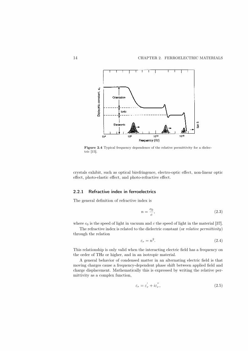
Figure 2.4 Typical frequency dependence of the relative permittivity for a dielec-tric [15].
crystals exhibit, such as optical birefringence, electro-optic effect, non-linear opticeffect, photo-elastic effect, and photo-refractive effect.
2.2.1 Refractive index in ferroelectrics
The general definition of refractive index is
n =c0
c, (2.3)
where c0 is the speed of light in vacuum and c the speed of light in the material [37].The refractive index is related to the dielectric constant (or relative permittivity)
through the relation
εr = n2. (2.4)
This relationship is only valid when the interacting electric field has a frequency onthe order of THz or higher, and in an isotropic material.
A general behavior of condensed matter in an alternating electric field is thatmoving charges cause a frequency-dependent phase shift between applied field andcharge displacement. Mathematically this is expressed by writing the relative per-mittivity as a complex function,
εr = ε′
r + iε′′
r , (2.5)

2.2. OPTICAL AND EO PROPERTIES OF FERROELECTRICS 15
where the real part (ε′
r) characterizes the displacement of the charges and theimaginary part (ε
′′
r ) the dielectric losses. The loss tangent is defined as
tan δ ,ε′′
r
ε′
r
. (2.6)
The relative permittivity is dependent on frequency, as shown in Fig. 2.4.Since light is an alternating electromagnetic wave with the electric and magnetic
field vibration directions mutually perpendicular to one another, the electric fieldinduces an electric polarization in a dielectric crystal and the light itself is influencedby the crystal. The alternating frequency of light is so high (λ = 500 nm correspondsto a frequency of approximately 600 THz) that only the electronic polarizationcan follow the electric field change. Thus the relative permittivity of an opticallytransparent crystal is small, typically smaller than 10.
At lower frequencies many ferroelectric materials can exhibit dielectric constantsin the order of 5 000 or more. From this we understand that all the mechanisms(except electronic polarization) leading to high polarizability and high dielectricconstant, that is ionic, dipolar, and space charge, are effectively clamped at opticalfrequencies.
That the refractive index is a function of wavelength is known as material dis-persion at optical frequencies. For consistency the wavelength has to specified whenstating the refractive index.
2.2.2 Optical birefringence
In a microscopically anisotropic medium, the refractive index is different in differ-ent crystal directions. Ferroelectric materials can be both optically isotropic andoptically anisotropic. Ferroelectric ceramics are an example of the former type;their isotropic behavior is due to the random orientation of the grains they possess.The latter type can be divided into optically uniaxial and optically biaxial crystals.Let a coordinate system be chosen to coincide with the three principal axes of acrystal. Then we have the following relations
εx = n2x, εy = n2
y, εz = n2z. (2.7)
The optical anisotropy of a crystal is characterized by an index ellipsoid (oroptical indicatrix ) defined as
x2
n2x
+y2
n2y
+z2
n2z
= 1, (2.8)
where nx, ny, and nz are the principal refractive indices, as shown in Fig. 2.5. Theindex ellipsoid is mainly used to find the two indices of refraction associated withthe two independent plane waves that can propagate along an arbitrary directionk in a crystal. The idea is as follows: Find the intersection ellipse between a plane

16 CHAPTER 2. FERROELECTRIC MATERIALS
k
z
y
x
θ
ne(θ) no
ny
nx
nz
Figure 2.5 Optical indicatrix or index ellipsoid for a uniaxial crystal, nx = ny 6=
nz . The optic axis is parallel to the z-axis.
through the origin that is normal to the direction of propagation k and the indexellipsoid. The two axes of the intersection ellipse are equal in length to 2n1 and2n2, where n1 and n2 are the two indices of refraction [38].
In the case of a biaxial system the refractive indices are different in all threeprincipal directions, nx 6= ny 6= nz, and there are two optical axes.3
For the common situation of a uniaxial crystal, we have nx = ny = no andnz = ne, where no and ne are the ordinary and extraordinary refractive indices,respectively. The refractive index along the optic axis corresponds to the extraordi-nary index, ne, and the refractive index perpendicular to the optic axis correspondsto the ordinary index, no.
The existence of two rays with different indices of refraction is called opticalbirefringence. The birefringence is usually defined as
∆n = ne − no. (2.9)
Since the value of ne may be either higher or lower than no, birefringence may takeon positive or negative values. If ∆n > 0, the crystal is said to be positive, whereasif ∆n < 0, it is said to be negative.
3The optic axis is the line in a birefringent crystal, in the direction of which no double refractionoccurs. A uniaxial crystal has one such line, a biaxial crystal has two.
2.2. OPTICAL AND EO PROPERTIES OF FERROELECTRICS 17
For light that is propagating in a direction different from the principal axes in auniaxial crystal, the situation becomes a somewhat more complicated. A light wavewith the wave vector k, as shown in figure 2.5, will have an the ordinary index thatis constant, whereas the extraordinary refractive index is dependent on the angle θas
1
n2e(θ)
=cos2 θ
n2o
+sin2 θ
n2e
. (2.10)
2.2.3 Electro-optic effect
When an external electric field is applied to a ferroelectric crystal, ion displacementis induced and the refractive index is changed (birefringence is induced). This is theelectro-optic effect, which is one of the nonlinear optic (NLO) effects ferroelectricmaterials may exhibit.
Generally, an applied optical or static electric field E will rearrange the chargedistribution in the crystal. In an macroscopic context the electro-optic effect canbe described starting from a power series expansion of the polarization P [39]
Pi = P 0i + ε0(χ
(1)ij + χ
(2)ijkEk + χ
(3)ijklEkEl + · · · )Ej , (2.11)
where χ(1) is the linear susceptibility and χ(2) and χ(3) are the second- and third-order nonlinear susceptibilities of the material.
In the limit of low electric field, Eq. (2.11) can be truncated linearly as
Pi = P 0i + ε0χ
(1)ij Ej , (2.12)
which for an isotropic material gives
n2 = ε = ε0
(
1 + χ(1))
. (2.13)
This describes the linear optical properties of a medium, as stated earlier.When a static field is applied to a second-order NLO material, the term in χ(2)
in Eq. (2.11) will result in a change in the complex refractive index, proportional tothe field – the linear electro-optic effect. This effect is also called the Pockels effectand describes a linear relationship between the induced change in birefringence(∆n) and the electric field (E).
In the same way the term χ(3) leads to a change in refractive index which isquadratic in the applied field – the quadratic electro-optic effect or the DC Kerreffect.
Returning to the linear electro-optic effect, this effect can be described by rota-tion and deformation of the index ellipsoid. Since the propagation characteristics incrystals are fully described by means of the index ellipsoid, the effect of an appliedelectric field is most conveniently described by changes in the constants 1/n2
x, 1/n2y,

18 CHAPTER 2. FERROELECTRIC MATERIALS
and 1/n2z. Due to the rotation of the ellipsoid, cross-terms have to be included. Fol-
lowing the notation in [9], the equation for the index ellipsoid in the presence of anelectric field is
B11x2 + B22y
2 + B33z2 + 2B23yz + 2B31zx + 2B12xy = 1, (2.14)
where the parameters Bij are functions of the electric field E. In order to couplethe six constants Bij to three components of E, 18 coefficients in the form of a6 × 3 matrix are needed
B11 − 1n2
x
B22 − 1n2
y
B33 − 1n2
z
B23
B31
B12
=
r11 r12 r13
r21 r22 r23
r31 r32 r33
r41 r42 r43
r51 r52 r53
r61 r62 r63
Ex
Ey
Ez
. (2.15)
The 6 × 3 matrix is called the electro-optic tensor r, with the elements rij calledthe electro-optic coefficients. The symmetry and physics of the crystal frequentlyreduce the complexity of Eq. (2.15).
The electro-optic coefficients for a materials is usually determined experimen-tally, but very recently Veithen et al. have presented a method to predict the linearEO coefficients of periodic solids using first principle calculations, explicitly takinginto account the electronic, ionic and piezoelectric contributions [40].
An example – LiNbO3
On of the most common electro-optic materials, LiNbO3, belonging to the trigonal3m point group, has electro-optic tensor in the form
r =
0 −r22 r13
0 r22 r13
0 0 r33
0 r51 0r51 0 0−r22 0 0
. (2.16)
It is often possible to avoid the complications of the cross-terms by applying theexternal field parallel to one of the main orientations of the crystal and by choosingthe corresponding polarization of the light. Applying the electric field along thec-axis of the LiNbO3 crystal (E = (0, 0, E)), nx and ny are identical to no, whilenz = ne propagates the extraordinary beam. Eqs. (2.14) and (2.15) reduce to
(
1
n2o
+ r13E
)
(x2 + y2) +
(
1
n2e
+ r33E
)
z2 = 1. (2.17)

2.2. OPTICAL AND EO PROPERTIES OF FERROELECTRICS 19
In this case the principal axes of the indicatrix only change their lengths, but theindicatrix is not rotated (no cross terms are included). This new index ellipsoidgives for no(E) and ne(E)
1
n2o(E)
=1
n2o
+ r13E, (2.18)
1
n2e(E)
=1
n2e
+ r33E, (2.19)
which, using the approximation 1√1+a
≃ 1 − a2 , gives
no(E) = no −1
2n3
or13E, (2.20)
ne(E) = ne −1
2n3
er33E. (2.21)
The observed index changes are generally very small. As the electrical breakdownof LiNbO3 limits the usable fields to approximately 10 V/µm, a maximum indexchange of around 1.65 × 10⁻³ is possible [41].
Sometimes the linear electro-optic effect of a material is characterized by acommon linear electro-optic coefficient rc stated as
rc = −2∆n
n3E. (2.22)
The quadratic relationship between ∆n and E is similarly characterized by thequadratic electro-optic coefficient R given as
R = − 2∆n
n3E2. (2.23)
More importantly, the quadratic dependence of E implies that also an oscillating(optical) field induces changes in refractive index with a constant component. Withthird-order NLO materials, it is therefore possible to build all-optical or opto-opticalapplications [39].
2.2.4 Second harmonic generation
Substitution of a strong, sinusoidal electric field, E = E0 cos ωt, along the z-axisinto the second order term of Eq. (2.11) reveals a contribution to the inducedpolarization
P(2)i = ε0χ
(2)izzE
20(cos ωt)2 =
1
2ε0χ
(2)izzE
20(1 + cos 2ωt), (2.24)
which contains a dc component and a component twice the applied frequency.The second term shows that the induced dipole will also have a 2ω component.
This oscillating macroscopic polarization acts as a source of radiation at 2ω. In a

20 CHAPTER 2. FERROELECTRIC MATERIALS
macroscopic noncentrosymmetric medium, this leads to the generation of a coherentbeam at 2ω. This is the frequency doubling or second-order harmonic generation(SHG), which is employed in wavelength converters for generation of shorter wave-length laser light [10, 11, 42–44]. Analogously, the third-order term will lead tocontributions at 3ω, leading to third-order harmonic generation (THG) [45].
2.2.5 Photo-elastic effect
The photo-elastic effect (also called elasto-optic or piezo-optic effect) in a materialcouples mechanical strain to the optical index of refraction. The effect is char-acterized by a strain-optic tensor and may occur in all crystals, including non-ferroelectrics and ferroelectrics. The effect has significant practical importance,since it allows for the interaction of acoustic and optic waves and makes possiblethe acousto-optic modulation of light. Particularly, the effect is important for mate-rials with a morphotropic phase boundary (MPB),4 around which the piezoelectriccoefficients and the electromechanical coupling factors are anomalously large. Thisis because the polar vector of domains changes orientation spontaneously whenthe ferroelectric phase boundary is crossed, and thus for compositions close to theboundary it is quite easy for an electric field to tilt the polar vector [46]. Around theMPB, field-induced strain enhances the refractive index change via the photo-elasticeffect.
Photo-refractive effect
The photo-refractive effect refers to optically induced changes of refractive indexwhich occur in many spontaneously polarized materials [21]. The effect was firstreported in LiNbO3 and LiTaO3 using focused laser beams in the blue and greenregions of the spectrum [47]. Chen proposed that free carriers excited in the il-luminated regions of a crystal were displaced along the polar axis of the crystalto trapping cites, where the resulting space-charge fields are giving rise to an in-dex change via the electro-optic effect [48]. Thus the necessary conditions for thephoto-refractive effect in an electro-optic host are:
• A suitable combination of incident wavelength and absorbing centers whichare photoionized by the radiation. This requirement is fulfilled either byextrinsic impurities or defects, e.g., doping, or by intrinsic absorption acrossthe band gap.
• Suitable trapping cites. This is satisfied by multivalent impurities.
• Free carrier transport to generate the internal fields. This implies that thefree carriers are sufficiently mobile to reach the trapping cites before recom-bination.
4A morphotropic phase boundary is in general considered as a special transitional regionbetween the tetragonal and rhombohedral phases, where both the phases are observed.

2.2. OPTICAL AND EO PROPERTIES OF FERROELECTRICS 21
Figure 2.6 Schematic description of different types of defects in deposited oxidethin films [15].
The photo-refractive effect has also been observed in, e.g., BaTiO3, K(Ta,Nb)O3,Pb1−xLax(Zry,Ti1−y)1−0.25xO3 and SrxBa1−xNb2O6 [21].
2.2.6 Optical absorption
In fact, there is no medium which is totally transparent in the entire range ofthe electromagnetic spectrum. Among the ionic crystals which are transparent inthe visible range, some may be transparent in the infrared region but opaque inthe ultraviolet region. Crystals composed of oxygen octahedra (e.g. titanates andniobates) are good examples of this case [22]. Some ionic crystals, especially thedoped ones, exhibit a few narrow absorption peaks in an otherwise transparentregion (the frequencies of the absorption peaks in the infrared region correspond tothe lattice vibration frequencies). Absorption in films may also result from oxygendeficiency, leading to mixed valencies and charge-transfer electronic transitions,and other stoichiometric defects [49]. The optical absorption is naturally of highimportance for optical applications.
2.2.7 Optical scattering
Optical scattering is a serious problem in the integration of dielectric oxide materialsin applications, as it is the predominant loss mechanism. Scattering can be subdi-vided into volume and surface scattering. Surface scattering losses are attributedto both light scattered from the film surface and the film/substrate interface, wherethe main contribution comes from the film surface. For waveguide applications ithas been estimated that the surface rms roughness needs to be of the order of 1 nmor below to achieve low (below 1 dB/cm) surface scattering losses [50,51].
Volume losses originate from scattering due to imperfections such as point de-fects, dislocations, vacancies, and grain boundaries, found in the bulk of the wave-
22 CHAPTER 2. FERROELECTRIC MATERIALS
guide [50]. Fig. 2.6 depicts different defects that can occur in deposited films. Thereis a demand for high crystalline quality, since polycrystalline materials frequentlyshow strong scattering due to grain boundaries.
2.3 Materials
Several hundred ferroelectric and antiferroelectric materials have been reported [52,53]. By varying the compositions of these materials virtually thousands of materialshave been investigated. These materials can be divided into three main types:
• Compounds with corner sharing oxygen octahedrons, which are ionic crystals.
• Compounds containing hydrogen bonded radicals, where ferroelectricity iscreated by a preferential occupation of the hydrogen sites within the hydrogenbonds.
• Organic polymers.
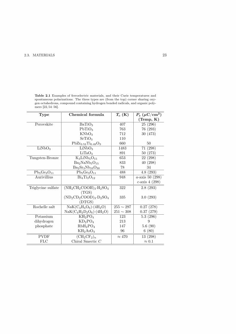
These main types can then be divided into several subgroups, see Tab. 2.1 [22,54–56].
Ferroelectric materials may exist as single crystals, in ceramic form, or as poly-crystalline or epitaxially grown thin films. The material properties depend on theform of the material. The rest of this chapter will focus on thin films for opti-cal applications, but it will include some notes about single crystals and ceramicmaterials as well.
2.3.1 Single crystals
Single crystalline is the purest form in which a material can exists. The micro-and macroscopic ordering is perfect in all three dimensions, except for impurities,vacancies, interstitials, and different forms of dislocations. The production of mostsingle crystals is a difficult process requiring significant technical skill.
The crystal growth process can be summarized by the following basic steps [39]:
• Transport of growth units in the growth medium.
• Diffusion and incorporation of growth units on the interface.
• Advancement of the interface leading to crystal growth.
The growth methods can be divided into two groups: heat transfer methods andmass transfer methods.
The heat transfer method uses temperature gradients to control the growth.This can be performed either by moving the crucible (Bridgeman-Stockberger Tech-nique) or by moving the crystal (Czochralski Crystal Pulling Technique).
The mass transfer method is using a concentration gradient to control thegrowth. This is performed by for example physical and chemical vapor transport,and solution growth.
2.3. MATERIALS 23
Table 2.1 Examples of ferroelectric materials, and their Curie temperatures andspontaneous polarizations. The three types are (from the top) corner sharing oxy-gen octahedrons, compound containing hydrogen bonded radicals, and organic poly-mers [22,54–56].
Type Chemical formula Tc (K) Ps (µC/cm2)(Temp, K)
Perovskite BaTiO3 407 25 (296)PbTiO3 763 76 (293)KNbO3 712 30 (473)SrTiO3 110
PbZr0.52Ti0.48O3 660 50LiNbO3 LiNbO3 1483 71 (298)
LiTaO3 891 50 (273)Tungsten-Bronze K3LiNb5O15 653 22 (298)
Ba2NaNb5O15 833 40 (298)Ba2Sr3Nb10O30 78 34
Pb5Ge3O11 Pb5Ge3O11 488 4.8 (293)Aurivillius Bi4Ti3O12 948 a-axis 50 (298)
c-axis 4 (298)
Triglycine sulfate (NH2CH2COOH)3·H2SO4 322 2.8 (293)(TGS)
(ND2CD2COOD)3·D2SO4 335 3.0 (293)(DTGS)
Rochelle salt NaK(C4H4O6)·(4H2O) 255 ∼ 297 0.27 (278)NaK(C4H2D2O6)·(4H2O) 251 ∼ 308 0.37 (279)
Potassium KH2PO4 123 5.3 (296)dihydrogen KD2PO4 213 9phosphate RbH2PO4 147 5.6 (90)
KH2AsO4 96 6 (80)
PVDF (CH2CF2)n ≈ 470 13 (298)FLC Chiral Smectic C ≈ 0.1
24 CHAPTER 2. FERROELECTRIC MATERIALS
2.3.2 Ceramics
A ceramic consists of randomly oriented crystallites. The properties of ceramicmaterials are strongly influenced by the manufacturing process.
In general fabrication of ferroelectric oxide ceramics includes the following steps:
• removal of crystal water
• weighing of raw materials
• ball milling
• calcining
• secondary grinding
• shaping by mould-pressing or roll-pressing
• sintering
• poling
The first step of the process is to weigh the raw powders in stoichiometric propor-tions. The raw materials are often highly purified oxides. The purer the powder,the easier to control the quality of the resulting ceramic.
The powders are then mixed and ball-milled to form an intimate mixture atvery fine particle size. The drawbacks here are that the milling process does noteffectively give particles of size less than approximately 1 µm and that there willbe some contamination from the milling media.
After mixing and grinding, the mixture is usually pressed into lumps and cal-cined at elevated temperatures (in the range of 1000 C) to produce the desiredcompound by combination reaction. The compound so obtained must be ground asecond time in order to be homogenized before shaping and sintering.
Various methods, such as mould-pressing, roll pressing, or hydrostatic pressing,may be employed to create the desired shapes. Usually an organic binder is addedto simplify shaping. The binding agent is then removed by slowly heating thesample. Finally, the material is sintered at elevated temperature (higher than thecalcining temperature) to form the final ceramic. For oxides it is necessary to havean oxidizing atmosphere or air during the sintering process.
A measure of the quality of the ceramic sample is given by a comparison tothe theoretical density. The density of the sample is measured and compared withthe value for the corresponding single crystal. Generally, the closer to theoreticaldensity, the better prepared ceramic sample.
Coprecipitation is an alternative method to form ceramics. The method includesadding a precipitate into a liquid solution of mixed metal salts, which produces ahomogeneous precipitate. Then thermal dissolution forms homogeneous powdersfrom the precipitate.
2.3. MATERIALS 25
Yet another method is the alkoxide hydrolysis, or sol-gel method. Metal alkoxidesare mixed in alcohol in appropriate proportions. When water is added, a hydrolyticreaction produces alcohol and metal hydroxide. The metal hydroxide is filtered,dried and heated to produce the ceramic oxides. The method can produce very finepowder of high purity and thus high-performing ceramics, and it is even used tomake thin films.
2.3.3 Thin films
Thin film technology is the backbone of modern electronic material manufacturing.As the name suggests, very thin layers of material are deposited on or prepared ontoa thicker, stabilizing substrate, which often is a single crystal of some other material.The thickness of the thin films is on a scale of micrometers or less. In order to makehigh-performance materials, it is often crucial to grow epitaxial films, where bulk-like properties can be achieved. Epitaxy is a process where a single crystal layeris deposited on a single crystal substrate. The word epitaxy is derived from twoGreek words: epi, which means "upon", and taxis, which means "arranged". Thus,epitaxy is the arrangement of atoms on an ordered substrate, which act as the seedcrystal. It is not necessary for the film and substrate to be of the same material.When the layer and the substrate are not of the same composition, the depositionis called heteroepitaxy.
Several ferroelectric thin films have been investigated for a wide variety of elec-trical and optical applications in the past three decades. Some of the reasons forthe increasing importance of ferroelectric thin films are:
• The trend toward miniaturization of electronic components. This also effectsferroelectric devices, where a thin film device has just a fraction of the vol-ume compared to bulk ceramics or single crystals. Thin film materials offerthe potential for increased speeds, reduced driving voltages, and enhancedefficiencies.
• Thin films have design advantages, such as large geometrical flexibility, com-pared to single crystals. They also offer the potential for monolithic integra-tion with electronic and optoelectronic devices and systems.
• Thin films are generally not as expensive as single crystals.
• New areas of application are being identified that utilize new device concepts,exploiting properties that are unique to both thin films and ferroelectric ma-terials.
There are a wide variety of techniques to grow thin films on single crystal sub-strates. A few of these techniques are reviewed in Chapt. 3.
26 CHAPTER 2. FERROELECTRIC MATERIALS
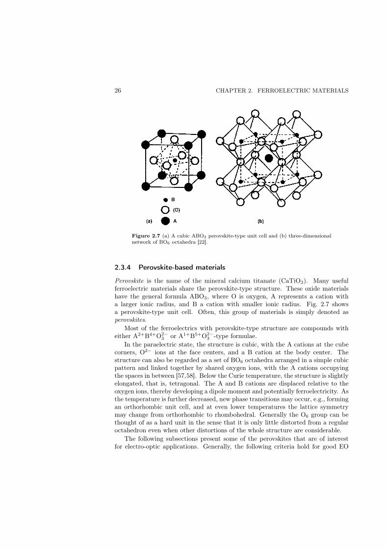
Figure 2.7 (a) A cubic ABO3 perovskite-type unit cell and (b) three-dimensionalnetwork of BO6 octahedra [22].
2.3.4 Perovskite-based materials
Perovskite is the name of the mineral calcium titanate (CaTiO3). Many usefulferroelectric materials share the perovskite-type structure. These oxide materialshave the general formula ABO3, where O is oxygen, A represents a cation witha larger ionic radius, and B a cation with smaller ionic radius. Fig. 2.7 showsa perovskite-type unit cell. Often, this group of materials is simply denoted asperovskites.
Most of the ferroelectrics with perovskite-type structure are compounds witheither A2+B4+O2−
3 or A1+B5+O2−3 -type formulae.
In the paraelectric state, the structure is cubic, with the A cations at the cubecorners, O2− ions at the face centers, and a B cation at the body center. Thestructure can also be regarded as a set of BO6 octahedra arranged in a simple cubicpattern and linked together by shared oxygen ions, with the A cations occupyingthe spaces in between [57,58]. Below the Curie temperature, the structure is slightlyelongated, that is, tetragonal. The A and B cations are displaced relative to theoxygen ions, thereby developing a dipole moment and potentially ferroelectricity. Asthe temperature is further decreased, new phase transitions may occur, e.g., formingan orthorhombic unit cell, and at even lower temperatures the lattice symmetrymay change from orthorhombic to rhombohedral. Generally the O6 group can bethought of as a hard unit in the sense that it is only little distorted from a regularoctahedron even when other distortions of the whole structure are considerable.
The following subsections present some of the perovskites that are of interestfor electro-optic applications. Generally, the following criteria hold for good EO
2.3. MATERIALS 27
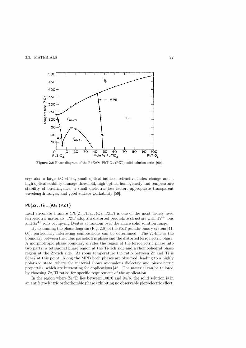
Figure 2.8 Phase diagram of the PbZrO3-PbTiO3 (PZT) solid-solution series [60].
crystals: a large EO effect, small optical-induced refractive index change and ahigh optical stability damage threshold, high optical homogeneity and temperaturestability of birefringence, a small dielectric loss factor, appropriate transparentwavelength ranges, and good surface workability [59].
Pb(Zrx,Ti1−x)O3 (PZT)
Lead zirconate titanate (Pb(Zrx,Ti1−x)O3, PZT) is one of the most widely usedferroelectric materials. PZT adopts a distorted perovskite structure with Ti4+ ionsand Zr4+ ions occupying B-sites at random over the entire solid solution range.
By examining the phase diagram (Fig. 2.8) of the PZT pseudo-binary system [41,60], particularly interesting compositions can be determined. The Tc-line is theboundary between the cubic paraelectric phase and the distorted ferroelectric phase.A morphotropic phase boundary divides the region of the ferroelectric phase intotwo parts: a tetragonal phase region at the Ti-rich side and a rhombohedral phaseregion at the Zr-rich side. At room temperature the ratio between Zr and Ti is53/47 at this point. Along the MPB both phases are observed, leading to a highlypolarized state, where the material shows anomalous dielectric and piezoelectricproperties, which are interesting for applications [46]. The material can be tailoredby choosing Zr/Ti ratios for specific requirement of the application.
In the region where Zr/Ti lies between 100/0 and 94/6, the solid solution is inan antiferroelectric orthorhombic phase exhibiting no observable piezoelectric effect.

28 CHAPTER 2. FERROELECTRIC MATERIALS
Around both Zr/Ti 94/6 and 53/47, PZT shows high pyroelectric coefficients.Doping PZT material with donor or acceptor ions changes its properties dra-
matically, see for example the PLZT materials below.Synthesis of PZT thin films has been performed using a variety of techniques
such as sputtering, metalorganic chemical vapor deposition, pulsed laser deposi-tion, sol-gel deposition, and liquid phase epitaxy. The resulting properties havebeen studied extensively, see for example [61–63]. In particular the electro-opticalproperties have been reported by Land [64] and Potter et al. [65]. PZT films havealso been deposited on Si using a SrTiO3 template layer [8].
There are many potential applications for thin film PZT materials including non-volatile memory elements, electro-optic waveguide modulators, and pyroelectric IRdetectors. As ceramic, the material is widely used in piezoelectric sensors andactuators.
Pb1−xLax(Zry,Ti1−y)1−0.25xO3 (PLZT)
Lanthanum-modified lead zirconate-titanate, Pb1−xLax(Zry,Ti1−y)1−0.25xO3 or PL-ZT, is an interesting class of materials because of its pronounced electro-optic char-acteristics and high optical transparency [37,66,67]. For simplicity the compositionsare designated by the proportional parts x/y/z of the constituent La/Zr/Ti ions.The material has been investigated both in bulk and thin film form. Thin filmshave been deposited on various oxide and semiconductor substrates using differ-ent deposition techniques such as magnetron sputtering, ion beam sputtering, andpulsed lased deposition. Strong second-harmonic generation has been reported at1.06 µm incident wavelength [43].
Many groups have investigated the electro-optic properties of PLZT thin filmsgrown on sapphire [68,69], fused silica [70], glass [71,72], and silicon substrates [73,74]. Field-induced birefringence shifts as large as ∆n = 1.8 × 10⁻² have beenreported. Nashimoto has reported on very low propagation loss (<0.1 dB/cm)bilayer optical waveguide with an effective electro-optic coefficient of 45 pm/V atλ = 1.55 µm [75].
PLZT has also been suggested in a thin ferroelectric interferometer for spatiallight modulators [76].5
BaTiO3 (BTO)
Barium titanate (BaTiO3, BTO) was the first ferroelectric perovskite to be dis-covered (in 1945), and it is up to present the most investigated ferroelectric mate-rial [77]. Bulk photo-refractive barium titanate single crystals are currently usedin a wide range of non-linear optical applications. The interest in this material is
5The spatial light modulator (SLM) is an electro-optical device that can convert an incoherentimage to a coherent image. The SLM is used for object recognition such as finger print matching,optical computing, optical communications, and adaptive optics.

2.3. MATERIALS 29
due to its very large electro-optic coefficient r51 = 1640 pm/V, which is one of thelargest values known for any material [78].
BTO thin films have been grown on MgO using metalorganic chemical vapordeposition [79] and pulsed laser deposition [80]. The choice of MgO as substrateis due to its lower refractive index and its optical transparency. For PLD-madefilms the optical birefringence has been estimated to ∆n = 0.014, which is lowerthan the bulk value of approximately ∆n = 0.05. The losses in a 600 nm thickfilm has been evaluated to 2.9 dB/cm. BTO has been deposited directly on Si [81]by molecular-beam epitaxy and recently also by pulsed laser deposition on GaAssubstrates using a MgO buffer layer [7, 82,83].
Choi et al. have shown that biaxial strain in BTO films deposited on closelylattice-matched substrates can significantly enhance the ferroelectric properties ofthe material [84]. This strain engineering can be used to tailor the ferroelectricphase transition temperature and improve the EO coefficients.
Closer to applications, Gill et al. have made a channel waveguide modulator onMgO with reff ≈ 50 pm/V at dc fields and reff ≈ 18 pm/V at 5 MHz for λ around1.55 µm [85]. More recently, a Mach-Zehnder optical waveguide modulator has beenfabricated by ion-beam etching of BaTiO3 thin films on MgO substrates [86, 87].The optical waveguide propagation losses were 2-3 dB/cm and the field-inducedelectro-optic Pockels coefficient r51 = 86 pm/V was extracted by modeling at λ =633 nm. Similarly, a single mode strip-loaded waveguide design with low losses(≈1 dB/cm) has been fabricated by Tang et al., showing an effective electro-opticcoefficient up to 162 pm/V at λ = 1.55 µm [88]. The waveguide structure consistedof an epitaxial BTO film on MgO, with a 4 µm wide and 125 nm thick Si3N4 strip ontop to confine the light, and a pair of coplanar electrodes (8 µm apart) [89,90]. Withthis structure broadband modulation out to 40 GHz has been observed togetherwith a low effective dielectric constant of εeff = 20.8 [91].
KNbO3
Perovskite structure niobates form one of the promising groups of ferroelectric mate-rials showing versatile dielectric, piezoelectric, pyroelectric, and electro-optic prop-erties.
Among the ferroelectric oxides, potassium niobate (KNbO3) has been shown tohave excellent electro-optic, nonlinear optic, and photo-refractive properties [78].High quality single crystals have been grown by various methods, such as the topseed solution growth technique [22].
Several techniques have been used to deposit KNbO3 on oxide substrates, suchas ion-beam sputtering [92,93], rf-diode sputtering [94], pulsed laser deposition [95],and metalorganic chemical vapor deposition [96,97]. A problem with sputtering ofa pure KNbO3 target is a severe deficiency of potassium in the resulting films. Thisdeficiency is due to the high volatility of potassium ions at elevated temperatures,and can be reduced by using potassium-enriched targets.

30 CHAPTER 2. FERROELECTRIC MATERIALS
The linear electro-optic coefficient of epitaxial KNbO3 on LaAlO3 substrates hasbeen determined to 12 pm/V at λ = 632 nm and 100 kHz by Hoerman et al. [97],whereas Graettinger et al. measured a quadratic-like dependence of birefringenceshift on applied electric field [92]. The dynamic response of the EO effect hasalso been analyzed [98]. Combining the low dielectric constants of KNbO3 withthe electro-optic coefficients which are comparable to PLZT, makes KNbO3 filmsbetter suited for high-speed switching applications.
KTaxNb1−xO3 (KTN)
The system of solid solutions KTaxNb1−xO3 (KTN) is ferroelectric for x . 0.95and exhibits several ferroelectric phases. By choosing the composition carefully, itis possible to make films close to the ferroelectric phase boundary.
Hoerman et al. have investigated KTN thin films on spinel (MgAl2O4) substratesby varying the tantalum concentration [99]. The effective electro-optic coefficientwas measured to as high as 40 pm/V (λ = 632 nm and 100 kHz) at concentrationscorresponding to room temperature phase boundaries of the KTN thin film system.KTN has also been successfully deposited on GaAs using buffer layers [6].
Recently, NTT Advanced Technology Corporation in Japan have developed agrowth technique to produce high-quality KTN single crystals. The crystals exhibitvery large quadratic electro-optic effect with reasonable bias voltage [100]. Thecrystal has been used to form a buried waveguide phase modulator [101,102].
NaNbO3
Sodium niobate (NaNbO3) is probably the most complex perovskite ferroelectricknown [21]. The high-temperature phase above 640 C is a simple cubic perovskiteas in the other perovskites in this section. Below 640 C, a whole series of struc-tural transitions ensues as the temperature is lowered, finally reaching a monoclinicferroelectric phase below about -100 C. At room temperature NaNbO3 is in anorthorhombic antiferroelectric phase, but a ferroelectric state can be induced bythe application of a strong electric field.
2.3.5 Na0.5K0.5NbO3 (NKN)
Ferroelectric sodium potassium niobate, NaxK1−xNbO3, is the continuous solid so-lution of KNbO3 and NaNbO3, and is perovskite structured for x < 0.97. Bulkceramic NaxK1−xNbO3 exhibits a complicated phase diagram with several struc-tural phase transition as shown in Fig. 2.9 [52, 103, 104]. In the vicinity of one ofits morphotropic phase boundaries, when x = 0.50, Na0.5K0.5NbO3 (NKN) showsthe highest electromechanical coupling coefficient and moderate dielectric suscep-tibility [105,106].
The ceramic properties have been studied in detail [105,107–109]. Tab. 2.2 showsa summary of the physical properties of air fired and hot pressed NKN ceramic
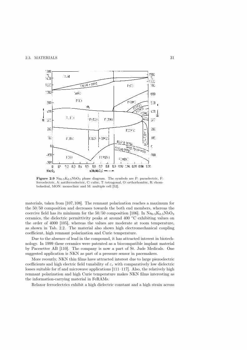
2.3. MATERIALS 31
Figure 2.9 Na0.5K0.5NbO3 phase diagram. The symbols are P: paraelectric, F:ferroelectric, A: antiferroelectric, C: cubic, T: tetragonal, O: orthorhombic, R: rhom-bohedral, MON: monoclinic and M: multiple cell [52].
materials, taken from [107,108]. The remnant polarization reaches a maximum forthe 50/50 composition and decreases towards the both end members, whereas thecoercive field has its minimum for the 50/50 composition [106]. In Na0.5K0.5NbO3
ceramics, the dielectric permittivity peaks at around 400 C exhibiting values onthe order of 4000 [105], whereas the values are moderate at room temperature,as shown in Tab. 2.2. The material also shows high electromechanical couplingcoefficient, high remnant polarization and Curie temperature.
Due to the absence of lead in the compound, it has attracted interest in biotech-nology. In 1999 these ceramics were patented as a biocompatible implant materialby Pacesetter AB [110]. The company is now a part of St. Jude Medicals. Onesuggested application is NKN as part of a pressure sensor in pacemakers.
More recently, NKN thin films have attracted interest due to large piezoelectriccoefficients and high electric field tunability of εr with comparatively low dielectriclosses suitable for rf and microwave applications [111–117]. Also, the relatively highremnant polarization and high Curie temperature makes NKN films interesting asthe information-carrying material in FeRAMs.
Relaxor ferroelectrics exhibit a high dielectric constant and a high strain across
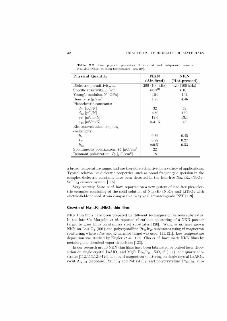
32 CHAPTER 2. FERROELECTRIC MATERIALS
Table 2.2 Some physical properties of air-fired and hot-pressed ceramicNa0.5K0.5NbO3 at room temperature [107,108].
Physical Quantity NKN NKN(Air-fired) (Hot-pressed)
Dielectric permittivity, εr 290 (100 kHz) 420 (100 kHz)Specific resistivity, ρ [Ωm] ≈1010 ≈1010
Young’s modulus, Y [GPa] 104 104Density, ρ [g/cm3] 4.25 4.46Piezoelectric constants:
d31 [pC/N] 32 49d33 [pC/N] ≈80 160g31 [mVm/N] 12.6 13.1g33 [mVm/N] ≈31.5 43
Electromechanical couplingcoefficients:
kp 0.36 0.45k31 0.22 0.27k33 ≈0.51 0.53
Spontaneous polarization, Ps [µC/cm2] 22Remnant polarization, Pr [µC/cm2] 18
a broad temperature range, and are therefore attractive for a variety of applications.Typical relaxor-like dielectric properties, such as broad frequency dispersion in thecomplex dielectric constant, have been detected in the lead-free Na0.5K0.5NbO3–SrTiO3 ceramic system [118].
Very recently, Saito et al. have reported on a new system of lead-free piezoelec-tric ceramics consisting of the solid solution of Na0.5K0.5NbO3 and LiTaO3 withelectric-field-induced strain comparable to typical actuator-grade PZT [119].
Growth of Na0.5K0.5NbO3 thin films
NKN thin films have been prepared by different techniques on various substrates.In the late 80s Margolin et al. reported rf cathode sputtering of a NKN powdertarget to grow films on stainless steel substrates [120]. Wang et al. have grownNKN on LaAlO3 (001) and polycrystalline Pt80Ir20 substrates using rf magnetronsputtering, where a Na- and K-enriched target was used [111,121]. Low temperaturedeposition was studied by Kugler et al. [122]. Cho et al. have made NKN films bymetalorganic chemical vapor deposition [123].
In our research group NKN thin films have been fabricated by pulsed laser depo-sition on single crystal LaAlO3 and MgO, Pt80Ir20, SiO2/Si(111), and quartz sub-strates [112,113,124–126], and by rf magnetron sputtering on single crystal LaAlO3,r-cut Al2O3 (sapphire), SrTiO3 and Nd:YAlO3, and polycrystalline Pt80Ir20 sub-
2.3. MATERIALS 33
strates [116,127–130].
2.3.6 Other corner sharing octahedra
There are a few ferroelectric oxide materials that have other corner sharing octa-hedrons than in the perovskite structure. The most prominent are lithium niobateand lithium tantalate [21, 22], where the crystal can be described by a hexagonalcell structure belonging to the 3m point group. In practice, the orientation of thecrystal samples are referred to a Cartesian coordinate system x, y, z as follows: thex-axis is along the a-axis of the hexagonal crystal cell, the z-axis is along the c-axis of the cell, and the y-axis is perpendicular to both the x- and z-axes. Forelectro-optic application tetragonal Tungsten Bronze-type SrxBa1−xNb2O6 is alsoof great interest. The Tungsten Bronze-type structure is more complicated thanthe perovskite structure, as described in [21].
LiNbO3
Among all the ferroelectric materials, linear and non-linear electro-optic effects,and photo-refractive effects have been studied most extensively in lithium niobate(LiNbO3). The single crystal is uniaxial with no = 2.286, ne = 2.200 at λ =632.8 nm, and has high optical transparency in a wide frequency range. Comparedto for example BaTiO3, LiNbO3 has a relatively small electro-optic coefficients(r33 = 30.9 pm/V, r51 = 32.6 pm/V).
High quality LiNbO3 single crystals are grown from a melt by the Czochralski’stechnique. The diameter of the pulled crystal can be larger than 60 mm. Thepulled crystal usually has a polydomain structure, which is made single-domain bya poling process.6
LiNbO3 thin films have been successfully grown on sapphire substrates by sev-eral different deposition techniques, such as molecular beam epitaxy, liquid phaseepitaxy, rf- and magnetron sputtering, metalorganic chemical vapor deposition, sol-gel deposition, and pulsed laser deposition, see e.g. [131–133]. The main obstacle ingrowing LiNbO3 is keeping high crystal (and thus optical) quality when the thick-ness exceeds 250 nm, mostly because of the large vapor pressure gradient between Liand Nb. To get around this a multi-step process has recently been proposed [133],where waveguide losses for a 630 nm thick film were calculated to 1.2 dB/cm atλ = 632.8 nm. LiNbO3 has also been deposited on Si [134] and GaAs [135] withand without a MgO buffer layer.
A quadratic electro-optic behavior has been measured in pulsed laser depositedLiNbO3 films on sapphire substrates [136].
6In a poling process the domains are aligned using an applied electric field.
34 CHAPTER 2. FERROELECTRIC MATERIALS
SrxBa1−xNb2O6 (SBN)
Strontium-barium niobate (SrxBa1−xNb2O6, 0.25 ≤ x ≤ 0.75, SBN) crystals canbe grown in excellent optical quality [78]. The crystals exhibit very large EO coef-ficients; in fact they are about ten time larger than those for LiNbO3. Thin films,preferably on MgO substrates for epitaxial growth, have been prepared with vari-ous techniques, such as liquid phase epitaxy, rf sputtering, metalorganic chemicalvapor deposition, sol-gel deposition, and pulsed laser deposition [78]. SBN75 onMgO has shown very high diagonal Pockel’s coefficient, r33 = 844 pm/V [137],and pronounced SHG [138]. SBN has been deposited by pulsed laser deposition onSiO2-coated Si [139].
2.3.7 Organic polymers
In a quite different approach, electro-optic organic polymers have been suggestedas a modulator material. They have advantages such as low dispersion in theindex of refraction between infrared and millimeter-wave frequencies. They canbe deposited and will adhere to many substrates including semiconductors, andthey can be integrated into an optical circuit which includes other optical materi-als [140]. Among the disadvantages are the difficulties in the chemical synthesis.Electro-optic polymers require highly optically nonlinear chromophores which canbe incorporated into a polymer host, aligned by a poling electric field, and finallyhardened to maintain the alignment.
Among the studied polymer materials, copolymers of vinylidene fluoride andtrifluorethylene, P(VDF-TrFE) have been commercialized [141] and many ideashow to develop a Mach-Zehnder modulator have been published, see for exam-ple [142–146]. Strong linear electro-optic effect has been reported in single-crystalN-(4-nitrophenyl)-(L)-prolinol (NPP) grown by a modified Bridgeman method [147]and in single crystal 4-dimethylamino-N-methyl-4-stilbazolium (DAST) [148, 149].Recently, physical vapor deposition of new heteroaromatic-based chromophore as-semblies showing very large optical nonlinearities was reported [150].
Another group of materials with pronounced electro-optic effects are the ferro-electric liquid crystals. In a chiral smectic7 C-phase liquid crystal, rod-like mole-cules are arranged in layers with the long molecular axes (director n) parallel to oneand another but tilted by an angle θ0 from the normal to the layer. The directorn can be switched by applying an external electric field along the smectic layers.This will change the optical properties as discussed in [22].
7Chiral implies that no mirror symmetry exists in the molecules that forms the liquid crystal.Smectic is a phase of a liquid crystal, where the molecules are piled in two-dimensional layers.

Chapter 3
Growth Techniques and Processing
The controlled deposition of functional thin-film layers on different substrates isa very important step in manufacturing integrated circuits in the semiconductorindustry as well as in developing new oxide materials for potential integration withexisting semiconductors. There are a wide variety of techniques to grow thin filmson single crystal substrates. The methods for deposition are dominated by thedeposition from the vapor phase and they fall into three broad categories, namelychemical vapor deposition (CVD), physical vapor deposition (PVD), and overlap-ping techniques that combine both physical and chemical processes. In the physicalapproach, material is deposited from a vapor or liquid containing atoms or ions ofthe material. In the chemical process, there is a chemical reaction at or very nearthe substrate or film surface, in which the deposited species are produced.
In semiconductor processing, the major deposition techniques for epitaxial filmsare liquid-phase epitaxy (LPE), vapor-phase epitaxy (VPE), and molecular-beamepitaxy (MBE). For oxide materials, the most common methods are physical vapordeposition methods such as vacuum evaporation and sputtering. In this chapter, rf-magnetron sputtering and pulsed laser deposition (PLD), the two techniques usedto deposit our Na0.5K0.5NbO3 films, will be described in some detail. The chapteralso includes a short section on target preparation.
After depositing a thin film, various processing steps have to be made before,e.g., electrical characterization can be performed. In this chapter, a lithography liftoff process and a metallization process for electrical contacts will be reviewed.
3.1 Rf-magnetron Sputtering
Sputtering in general, and radio frequency (rf) magnetron sputtering in particular,is considered as one of the physical deposition methods that can be used in industrialmass production. The basic principle in a sputtering process is acceleration of ionsin an electric field toward a target of material to be deposited, where the ionssputter target atoms. The sputtered species then deposit onto a heated wafer
35

36 CHAPTER 3. GROWTH TECHNIQUES AND PROCESSING
(substrate), which is placed facing the target. In some situations, the substratemay also be positioned off axis, as discussed later in this chapter. The summary ofthe techniques given below is partly based on [41,151].
3.1.1 Sputtering process
The simplest sputtering system is called dc-sputtering. The target and substrateare put in a vacuum chamber. The system is pumped to high vacuum and an inertprocess gas, such as argon, is introduced into the chamber. A potential of severalhundred volts, generated from an external power source, is applied between thetarget and substrate. The target will be on the cathode side (negative potential)and the substrate on the anode side. In some configurations, the substrate is keptneutral, whereas the walls of the vacuum chamber will have the positive potential.The high potential between the anode and cathode will cause an ignition of a plasmadischarge through collision with high energy electrons. The positively chargedions will be accelerated by the electric field towards the target. These acceleratedparticles will collide with the target and because of their high energy they willsputter target material, mainly as neutral atoms. These atoms will arrive on theoften heated substrate surface and, due to their high energy, they will be ableto migrate along the surface to form a dense and smooth film. The discharge ismaintained as accelerated electrons continuously ionize new ions by collision withthe process gas.
As the plasma is well-conducting, there is no major potential drop in the plasmaregion and, due to different mobilities of electrons and ions, the main voltage dropis observed at the cathode. One drawback with the method is the uncontrolledresputtering of the deposited film by negative ions.
A general advantage with sputtering is that it allows the deposition of filmswith the same composition as the target. The sputtering yields are different fordifferent target atoms, but this difference is compensated by a good self-regulatingmechanism; the sputtering process has a very low penetration depth and thus atomsthat are eroding faster will, after a short initial time, reach lower concentration inthe sputtering region of the target. Therefore, a quasi-equilibrium state is arisen,where the difference in yield is compensated by enrichment.
3.1.2 Rf-sputtering
Dc-sputtering is working nicely as long as the target has at least a minimum elec-trical conductivity. For an insulating target this is a problem, since the surfacerapidly will build up a positive charge repelling incoming positive ions. A widelyused technique for oxide thin film fabrication is so called reactive sputtering, wherea metal target is sputtered in presence of oxygen diluted in argon. But if the metaloxide to be deposited is non-conductive, the target soon will become insulating, thusdc-sputtering does not work. The remedy to this issue is to use a high-frequencyplasma discharge. A typical radio frequency of 13.56 MHz is capacitively coupled

3.1. RF-MAGNETRON SPUTTERING 37
Plasma
13.56 MHz
Anode Cathode
Figure 3.1 Rf plasma sputtering system with rf matching network [152].
to the target causing only a small voltage drop across the electrode, as shown inFig. 3.1. The target is alternatively bombarded by positive ions and then by neg-ative electrons which neutralize the charge. Non-symmetries introduced by thecapacitive coupling of the rf generator and fast electrons will build up a negativepotential at the cathode as compared to the plasma potential during each cycle.Nevertheless, deposition rates are much lower than for dc-sputtering.
3.1.3 Magnetron sputtering
The degree of ionization of the atoms in the plasma is often below 1 %, hence causinga rather low sputter-deposition rate. One method to improve the ionization rateis to use magnetic fields, which will capture the electrons in helical paths closeto the target, yielding a much higher ionization probability. This also reduces theprobability of electron-ion recombination at the walls of the chamber. The relativelylarge mass of the ions will essentially prevent their trapping in the magnetic field.
A typical arrangement using permanent magnets with corresponding fields isshown in Fig. 3.2. The magnetron arrangement allows lower gas pressure anddeposition occurs at lower voltages; however one disadvantage with magnetronsputtering is the inhomogeneous erosion of the target, which is also shown in thefigure.
In our experiments, we have used a combination of rf- and magnetron sputtering(rf-magnetron sputtering), which makes use of the advantages of each method. Wehave a Leybold-Heraeus system with a 1 inch magnetron, and a 2 inches substrate

38 CHAPTER 3. GROWTH TECHNIQUES AND PROCESSING
Figure 3.2 A typical magnetron sputtering arrangement using permanent magnets.The corresponding magnetic fields and partial erosion are also depicted.
holder that can be position in both on- and off-axis symmetry. The maximumrf power is 150 W. A standard operating condition is described as follows: Thebackground pressure in the vacuum chamber was lower than 10−6 Torr. An oxygen-argon (1:3) – (1:5) gas mixture was introduced after pumping to build up a totalpressure of 60 mTorr. The rf power was 60 W and the substrate was heated to650 C during growth. The deposition rate was estimated to 6-7 Å/s. The filmswere in situ post-annealed at 540 C in a 700 Torr oxygen atmosphere for 10 minutesand slowly cooled to room temperature.
3.2 Pulsed Laser Deposition, PLD
Pulsed laser deposition (PLD) is a well developed method for thin film preparation,and since its success in growing high temperature superconductors, the method hasshown to be especially suited for deposition of oxides and multi-component materi-als. Conceptually and experimentally, PLD is a simple technique, but the ablationprocess is complicated. The setup consists of a target holder and a substrate holder(heater) inside a vacuum chamber. An external high-power pulsed laser vaporizesthe target materials, creating a plasma plume and a thin film deposits on the heatedsubstrate. The summary that follows here is mainly based on [41,153].
3.2.1 Description of the PLD system
A schematic picture of our PLD system is given in Fig. 3.3.

3.2. PULSED LASER DEPOSITION, PLD 39
Figure 3.3 Schematic view of a pulsed laser deposition system [15].
Short and energetic laser pulses are focused through an optical system onto thetarget. To get high photon absorption with the oxide target, UV wavelengths arepreferred. The most common laser type for PLD is the excimer laser, where thelasing comes from the transition of excited molecules to the ground state. Thesemolecules consists of a noble gas atom (e.g. Ar, Kr or Xe) and a halogen atom (e.g.Cl or F), and can only exist in an excited state. As soon as the molecules returnto the ground state they dissociate. A population inversion is thus easily createdthrough a high-voltage avalanche electric discharge, and consequently excimer laserswork in a pulsed mode, where they can achieve high energy transfer to the target.Our laser is a KrF* excimer laser with wavelength 248 nm and pulse duration 25 ns(Lambda Physik LPX 305iCC ). The laser pulse repetition rate is usually between10 Hz and 50 Hz for our depositions. Energy densities on the surface of the targetwere between 2 and 5 J/cm2 per pulse. During deposition the target is rotated, sothat successive pulses do not hit the same area.
The laser beam enters the vacuum chamber through a quartz window. Beforedeposition the system is pumped down to a pressure of 10−6 mbar and oxygen(processing gas) is let in to build up a background pressure of approximately 0.4mbar. As the laser hits the ceramic target, a plasma plume containing energeticneutral atoms, ions and molecules is created perpendicular to the target surface.This plasma reaches the substrate, and the thin film is formed. For growth ofepitaxial oxide thin films sufficient ion mobility is needed. This is provided by
40 CHAPTER 3. GROWTH TECHNIQUES AND PROCESSING
heating the substrate, in our case typically to 650 C.
Merits of PLD
The PLD method offers several advantages in the formation of multi-componentthin films. The most important advantage is the stoichiometric material transferfrom a complex multi-elemental ceramic target to the substrate. This feature allowspreparation of films with complex stoichiometries. With appropriate laser energyand wavelength almost all materials can be ablated and thin films formed. Alsorather high deposition rates can be achieved and in situ oxygen post-anneal is easilyperformed.
Demerits of PLD
Disadvantages with the PLD method includes the formation of droplets and thelack of uniformity over large areas due to narrow angular distribution of the plume.Homogeneous laser output is required to deposit high-quality films. Still splashing,or droplet formation, is present. The plume will not just contain atoms, ions andmolecules, but also small droplets, which will cause rough films and thus problems ofscattering and absorption in optical applications of the thin films. Several methodshave been developed to reduce this effect. Rotation of the target and scanningthe laser beam may reduce the droplet formation. A mechanical velocity filter canreduce the amount of heavier particles, since they travel at lower speed comparedto light atoms and ions. In off-axis PLD geometry the surface of the substrate isplaced parallel or even 180 away from the direction of the plume. The films willbe much smoother but the deposition rate is reduced.
3.3 Na0.5K0.5NbO3 Target Preparation
A high-quality target is essential for achieving single-phase films of correct struc-ture. The target should have the correct stoichiometry and have density as closeas possible to the theoretical density for a single crystal of the material. The mainsteps in the production are milling, calcination, pressing and sintering, see thesection on ceramics (2.3.2).
For our film deposition a 25 mm diameter high-density, single-phase ceramicNa0.5K0.5NbO3 target was used. It was made of stoichiometric amounts of Na2CO3,K2CO3 and Nb2O5 that were mixed and calcinated at 940 C to form Na0.5K0.5NbO3
following the reaction
Na2CO3 + K2CO3 + 2Nb2O5 =⇒ 4Na0.5K0.5NbO3 + 2CO2(g). (3.1)
The coarse-grained calcinated powder was ball milled for 24 h, dried, sieved andpressed with uniaxial and isostatic pressing. The target was sintered with pressure-less sintering for 4 h at 1125 C, resulting in a final density of 4.3 g/cm3, which isabout 95 % of the theoretical density.

3.4. PROCESSING OF NA0.5K0.5NBO3 FILMS 41
substrate thin film
1 mm
10 µm 4 µm
Au/Cr electrode
Figure 3.4 Schematic view of the IDC electrodes used for dielectric characteriza-tion.
3.4 Processing of Na0.5K0.5NbO3 Films
After deposition, including any post-annealing processes, various characterizationtechniques will be applied to the thin film. Some of the characterization, such as x-ray diffraction, atomic force microscopy, and prism-coupling (see Chapt. 4), can beperformed without further processing, whereas for example electrical characteriza-tion requires processing of metallic contacts. This section describes the fabricationof test structures for electrical and electro-optic characterization of Na0.5K0.5NbO3
films.
3.4.1 Lithography
Lithography describes a method where a pattern is defined on a sample. A litho-graphic system consists of a radiation source, a resist-coated sample and an image-control system, which regulates what part of the sample that will be illuminated.The resist is changed by the illumination. Depending on the type of resist, exposedor non-exposed areas can be removed by selective etching. The pattern in the resistcan now be transferred to the sample, either by a metallization step or by anotheretching step.
Optical lithography, with light as radiation source, is the most common type oflithography. As image control system a mask is usually utilized. Depending on howthe mask is used, one yields contact, proximity or projection lithography. Here anoptical contact mask process will be described, where the mask has a transparentcarrier layer and an opaque absorber layer.

42 CHAPTER 3. GROWTH TECHNIQUES AND PROCESSING
substrate thin film
4 mm
10 µm
2 mm
Au/Cr electrode
Figure 3.5 Schematic view of the coplanar electrodes used for electro-optic char-acterization in transmission.
Since we want to deposit a metal pattern directly onto the film surface, we usethe standard lithography technique of lift-off. The pattern for electrical character-ization consists of an interdigital capacitor (IDC) structure shown schematicallyin Fig. 3.4, and the pattern for electro-optic characterization consists of coplanarsurface electrodes shown in Fig. 3.5.
Process flow
The list below describes the flow for an image reversal lithography process. All thesteps were performed in a clean room environment.
1. Cleaning. The film was cleaned for 5 minutes in an ultrasonic bath of acetone,then rinsed in iso-propanol and de-ionized (DI) water, and finally dried withnitrogen.
2. Preparation before resist spinning. To further dry the thin film sample aftercleaning it was pre-baked at 110 C for 2 minutes. Thereafter the samplewas placed in an HMDS (Hexamethyldisilazane) environment for 2 minutesto create a good adhesion layer for the photoresist.
3. Resist spinning and baking. The film was spin-coated with a image rever-sal photoresist (AZ 5214E) at 4000 rpm for 30 seconds, resulting in an ap-proximately 1.4 µm thick uniform layer. The resist-coated sample was thensoft-baked on a hot-plate at 100 C for 1 minute.
3.4. PROCESSING OF NA0.5K0.5NBO3 FILMS 43
4. Exposure 1. The pattern was defined using a mask inserted into a KarlSüss MA6/BA6 mask aligner with UV-light exposure for 2 seconds (35-45 mJ/cm2).
5. Post-exposure baking. The film was baked for 1 minute on a hot-plate at120 C.
6. Exposure 2. The sample was flooded with UV-light for 20 seconds (150-500 mJ/cm2).
7. Developing. The exposed resist was developed in a solution containing 1 partdeveloper (Microposit 351) and 5 parts DI water for 40 seconds and thenrinsed in DI water and dried with nitrogen. The pattern was checked in anoptical microscope.
3.4.2 Metallization
The electrodes consisted of a thin layer of Cr (10 nm) covered by a thicker layerof Au (500 nm). The chrome layer is acting as an adhesive layer between theferroelectric thin film and the gold contact. Gold is chosen because of its highconductivity and oxidation resistance.
The metal deposition was performed by electron-beam evaporation.
3.4.3 Lift-off
In the lift-off process the remaining photoresist is resolved, thus removing the ex-cess metal, only leaving the electrodes on the surface of the thin film. To removethe resist, the film was put in an ultrasonic acetone bath for about 10 minutes,thereafter rinsed in iso-propanol (about 2 minutes) and DI water, and finally driedwith nitrogen. The result was inspected using an optical microscope. If all theresist had been removed and the contacts were good, the samples were ready fortesting.

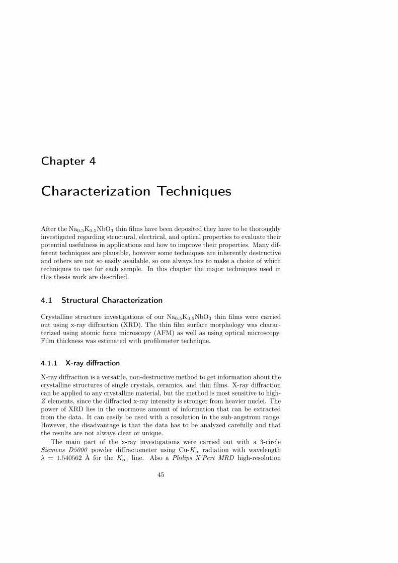
Chapter 4
Characterization Techniques
After the Na0.5K0.5NbO3 thin films have been deposited they have to be thoroughlyinvestigated regarding structural, electrical, and optical properties to evaluate theirpotential usefulness in applications and how to improve their properties. Many dif-ferent techniques are plausible, however some techniques are inherently destructiveand others are not so easily available, so one always has to make a choice of whichtechniques to use for each sample. In this chapter the major techniques used inthis thesis work are described.
4.1 Structural Characterization
Crystalline structure investigations of our Na0.5K0.5NbO3 thin films were carriedout using x-ray diffraction (XRD). The thin film surface morphology was charac-terized using atomic force microscopy (AFM) as well as using optical microscopy.Film thickness was estimated with profilometer technique.
4.1.1 X-ray diffraction
X-ray diffraction is a versatile, non-destructive method to get information about thecrystalline structures of single crystals, ceramics, and thin films. X-ray diffractioncan be applied to any crystalline material, but the method is most sensitive to high-Z elements, since the diffracted x-ray intensity is stronger from heavier nuclei. Thepower of XRD lies in the enormous amount of information that can be extractedfrom the data. It can easily be used with a resolution in the sub-angstrom range.However, the disadvantage is that the data has to be analyzed carefully and thatthe results are not always clear or unique.
The main part of the x-ray investigations were carried out with a 3-circleSiemens D5000 powder diffractometer using Cu-Kα radiation with wavelengthλ = 1.540562 Å for the Kα1 line. Also a Philips X’Pert MRD high-resolution
45
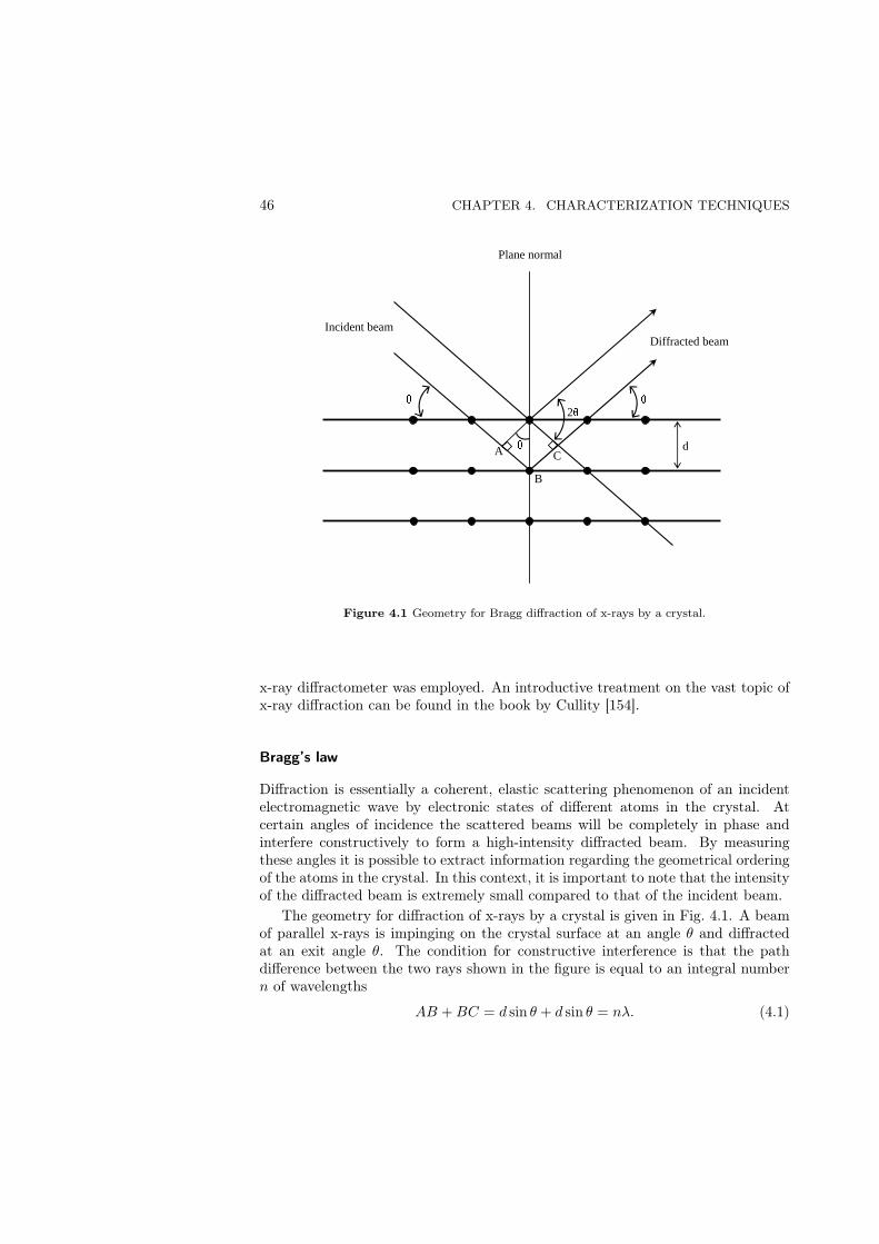
46 CHAPTER 4. CHARACTERIZATION TECHNIQUES
Plane normal
Incident beam Diffracted beam
2
C
B
A d
Figure 4.1 Geometry for Bragg diffraction of x-rays by a crystal.
x-ray diffractometer was employed. An introductive treatment on the vast topic ofx-ray diffraction can be found in the book by Cullity [154].
Bragg’s law
Diffraction is essentially a coherent, elastic scattering phenomenon of an incidentelectromagnetic wave by electronic states of different atoms in the crystal. Atcertain angles of incidence the scattered beams will be completely in phase andinterfere constructively to form a high-intensity diffracted beam. By measuringthese angles it is possible to extract information regarding the geometrical orderingof the atoms in the crystal. In this context, it is important to note that the intensityof the diffracted beam is extremely small compared to that of the incident beam.
The geometry for diffraction of x-rays by a crystal is given in Fig. 4.1. A beamof parallel x-rays is impinging on the crystal surface at an angle θ and diffractedat an exit angle θ. The condition for constructive interference is that the pathdifference between the two rays shown in the figure is equal to an integral numbern of wavelengths
AB + BC = d sin θ + d sin θ = nλ. (4.1)

4.1. STRUCTURAL CHARACTERIZATION 47
20 40 60 80 100 120
100
101
102
103
104
105
LAO
-004
004
LAO
-003
003
LAO
-002
002
LAO
-001
001
Rf-magnetron sputtered Na
0.5K
0.5NbO
3 on LaAlO
3
Inte
nsity
[cps
]
2θ [deg]
Figure 4.2 X-ray diffraction θ − 2θ pattern of a rf-magnetron sputteredNa0.5K0.5NbO3 thin film on a single crystal LaAlO3 (001) substrate. Note thelogarithmic scale in counts per second (cps).
Rewriting this formulates the famous Bragg’s law
nλ = 2d sin θ, (4.2)
where d is the distance between lattice planes and λ is the wavelength of the x-raybeam. The number n is called the order of diffraction and is conventionally includedin d.
Indexing lattice planes
A workable symbolism for the description of a plane in a lattice is the Miller indiceswhich are defined as
Miller indices. The reciprocals of the fractional intercepts which the plane makeswith the crystallographic axes.
For example, if the Miller indices of a plane are (hkl), then the plane makesfractional intercepts of 1/h, 1/k, and 1/l with the axes, and if the axial lengthsare a, b, c, the plane makes actual intercepts at a/h, b/k, and c/l. Parallel to anyplane in any lattice, there is a whole set of parallel equidistant planes, one of whichpasses through the origin. The Miller indices (hkl) usually refer to that plane inthe set which is nearest the origin. A negative Miller index is usually denoted by abar, e.g. a plane with h = 1, k = −2, and l = 2 has the Miller indices (122).
48 CHAPTER 4. CHARACTERIZATION TECHNIQUES
Plane normal
Diffracted beam +
Incident beam
2
Figure 4.3 Definition of angles in the 3-circle diffractometer: Here ω is the tiltingangle of the sample, 2θ the angle of the detector position, and ϕ the rotation of thesample perpendicular to its surface.
Epitaxial films
In our group, we have adapted a standard set of XRD measurements for a "fullcharacterization" of epitaxial thin films, as will be explained below.
As discussed in Sect. 2.3.3, a film is called epitaxial if the crystalline axes ofthe film coincide in orientation with the crystalline axes of the substrate at everyposition in the thin film. A thin film can be epitaxial but not single crystal inthe sense that grain boundaries are compatible with the notation of epitaxy. Eventhough neighboring grains often will include a small angle of misorientation, thefilm will still be called epitaxial.
θ − 2θ scan
The most common mode of operation in XRD characterization is the θ − 2θ scan,which can give information about crystalline orientation of the material in thegrowth direction (also called "out-of-plane" direction) and distances between latticeplanes parallel to the film surface. In this mode the incident angel θ is varied andthe detector angle for the diffracted beam is simultaneously moved uniformly at2θ. To collect maximal information, a θ− 2θ scan is usually performed over a wideangular range, say at least 20< 2θ < 100.

4.1. STRUCTURAL CHARACTERIZATION 49
Figure 4.4 Schematic description of the origin of broadening of XRD rocking curvedue to grain structure [15].
Fig. 4.2 displays a typical θ − 2θ diffraction pattern of an rf-magnetron sput-tered Na0.5K0.5NbO3 thin film on a single crystal LaAlO3 (001) substrate in therange 10< 2θ < 120. Only integer multiples of (001) reflections for the film andsubstrate can be observed, which implies that the film is exclusively (001) orientedin the growth direction, and that we observe no other phases. Thus the film isc-axis oriented. If the θ− 2θ scan is used to demonstrate the orientation and phaseof the film, it is preferable to show the data in logarithmic scale, as in Fig. 4.2.
Nelson-Riley extrapolation
In Fig. 4.2, four multiples of the (001) reflection are observed. Using the Nelson-Riley extrapolation function [154], the out-of-plane lattice parameter c can be de-termined with high accuracy. The procedure is as follows. First the thin film isadjusted so that the surface normal coincide as closely as possible with the diffrac-tometer axis. After that, an accurate θ− 2θ scan is performed and the c parameteris calculated for each reflection. Finally, the c parameters are plotted versus theNelson-Riley function and linearly extrapolated to a value at θ = 90. The Nelson-

50 CHAPTER 4. CHARACTERIZATION TECHNIQUES
10.0 10.5 11.0 11.5 12.0 12.5 13.00
25000
50000
75000
100000
125000
150000
175000
Rf-magnetron sputtered Na
0.5K
0.5NbO
3 on LaAlO
3
FWHM0.17°
FWHM0.60°
NKN-001
LAO-001
Inte
nsity
[cps
]
θ [deg]
Figure 4.5 XRD rocking curve (ω scan) and FWHM of the (001) Na0.5K0.5NbO3
film and LaAlO3 substrate reflections.
Riley function is given by
c = c0 − c0k
(
cos2 θ
sin θ+
cos2 θ
θ
)
, (4.3)
where c is the calculated lattice parameter from the measured Bragg peak, c0 the"true" fitted lattice parameter and k a fitting parameter. Note that Eq. (4.3) yields
c = c0 at θ = 90, thus in practice c is plotted versus(
cos2 θsin θ + cos2 θ
θ
)
and linearlyextrapolated to θ = 90 to determine c0. The origin of the Nelson-Riley function aresystematic errors in the lattice parameter due to misalignment of the instrument,surface shape of the sample, absorption in the sample, displacement of the samplefrom the diffractometer axis (usually the largest single source of error), and verticaldivergence of the incident beam.
Rocking curve – ω scan
An ω scan, or rocking curve, is performed to obtain information about the texturingor grain structure of the thin film layer. The 2θ angle is fixed corresponding to themaximum of a Bragg peak and the incident angle is varied ω around the θ angle,as shown in Fig. 4.3.
Even though a thin film may be single phase with almost perfect orientationin the growth direction, there can still be small deviations in the orientation ofthe different grains that the film consists of. This deviation is measured as a

4.1. STRUCTURAL CHARACTERIZATION 51
0 40 80 120 160 200 240 280 320 36010-1
100
101
102
103
104Rf-magnetron sputtered Na
0.5K
0.5NbO
3 on LaAlO
3
NK
N-1
03
LAO
-103
Inte
nsity
[cps
]
ϕ [deg]
Figure 4.6 XRD ϕ scan of the oblique (103) planes of the Na0.5K0.5NbO3 filmand LaAlO3 substrate, with detector positions 2θdet = 74.33, 79.97 and samplepositions θsam = 56.08, 58.73, respectively.
broadening of the rocking curve, as given theoretically in Fig. 4.4. The standardway of comparing rocking curves is to measure the full width at half maximum(FWHM). The narrower FWHM, the smaller deviation of the grain orientations.
Fig. 4.5 shows the rocking curve for the (001) Bragg reflections of film andsubstrate measured in Fig. 4.2, where θ + ω is designated just by θ as often isdone. For a more complete picture, it is always interesting to compare film andsubstrate FWHM of rocking curves, since instrumental broadening can affect themeasurements.
(θ + ω) − 2θ scan
The previous methods are only useful for investigating planes parallel to the filmsurface. For particular values of (θ +ω)− 2θ reflections from lattice planes inclinedan angle ω can be observed. The diffraction pattern looks similar to a standardθ−2θ scan, but can only be observed for special angles ϕ, see Fig. 4.3. These planesare often called oblique planes, and we have to estimate their positions and thenadjust the diffractometer accordingly. By investigating different oblique planes thein-plane lattice parameters can be estimated.

52 CHAPTER 4. CHARACTERIZATION TECHNIQUES
ϕ scan
In a ϕ scan, the sample is rotated around its surface normal, having the incidentbeam and detector positions fixed. From the scan, information of in-plane orienta-tion of grains, and relative in-plane orientation of grains compared to the substrates,can be collected. Fig. 4.6 shows a full 360 ϕ scan of the oblique (103) planes ofthe NKN film and LAO substrate measured in Fig. 4.2. A fourfold symmetry is ob-served, where the film and substrate peaks overlap to a high degree. This indicatesthat rf-magnetron sputtered Na0.5K0.5NbO3 films grow epitaxially cube-on-cubeonto the LaAlO3 substrate.
4.1.2 Atomic force microscopy
Scanning probe microscopy (SPM) refers to all techniques using a mechanism toscan a sharp tip across a sample surface at a very short distance to obtain 2-or 3-dimensional images of the surface at nanometer (or better) resolution bothlaterally and vertically. Atomic force microscopy (AFM) is one of these techniquesand operates by probing the force between a tip mounted on a special spring and thesurface. It is very sensitive in the vertical dimension and somewhat less sensitive inthe lateral dimension. This section includes a short introduction to the technique.Part of the information is taken from [41,155].
Theoretical principles
AFM operates by measuring the atomic forces between a probe and the sample.These forces depend on the type of sample and probe, distance between probe andsample, and sample surface contamination. In contrast to another common tech-nique, scanning tunneling microscopy, AFM does not require conducting samples,and is thus suitable for insulators, such as ferroelectric oxide thin films, as well asfor conductors.
The AFM instrument consists of a cantilever, usually formed from silicon, sili-con oxide, or silicon nitride, with a sharp tip mounted on its end. The tip is mostcommonly made from silicon nitride. Laser light is incident on the cantilever topand reflected to a segmented, position sensitive photodetector. The cantilever isbrought close to the sample surface and rastered in x−y direction using piezoelectricscanners. Holding the photodetector signal constant, equivalent to constant can-tilever deflection, by varying the sample height through a feedback arrangement,gives the vertical sample height variation compared to a base line.
An AFM can operate in several different modes. In contact mode the tip isbrought in contact with the sample surface. More commonly one uses tapping mode,where the tip is excited to vertical oscillations close to its resonance frequency. Asthe tip approaches the sample surface, the attractive forces increases causing aresonance frequency decrease. By keeping the amplitude constant, one also keepsthe tip-sample distance constant. The probe exerts negligible frictional force on thesample and the surface damage is minimal.
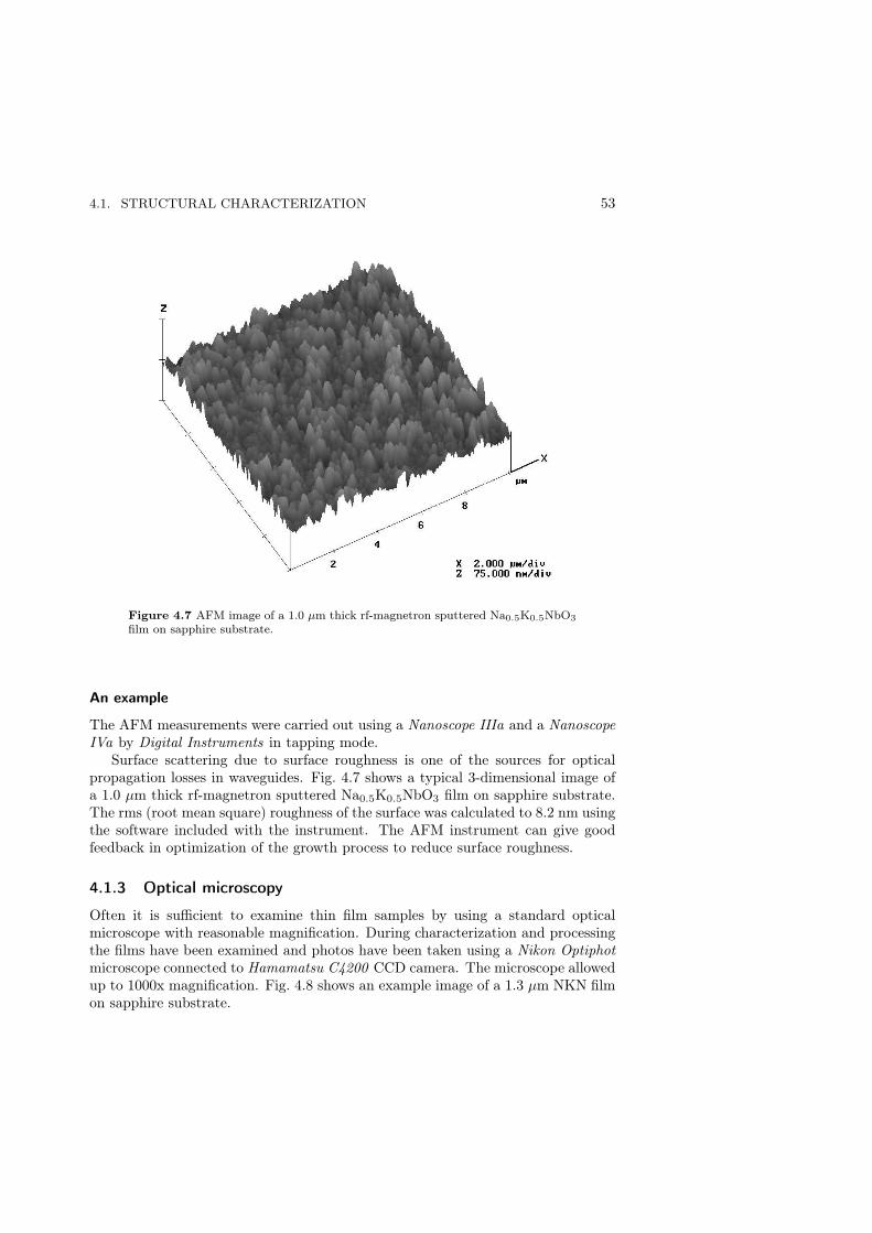
4.1. STRUCTURAL CHARACTERIZATION 53
Figure 4.7 AFM image of a 1.0 µm thick rf-magnetron sputtered Na0.5K0.5NbO3
film on sapphire substrate.
An example
The AFM measurements were carried out using a Nanoscope IIIa and a NanoscopeIVa by Digital Instruments in tapping mode.
Surface scattering due to surface roughness is one of the sources for opticalpropagation losses in waveguides. Fig. 4.7 shows a typical 3-dimensional image ofa 1.0 µm thick rf-magnetron sputtered Na0.5K0.5NbO3 film on sapphire substrate.The rms (root mean square) roughness of the surface was calculated to 8.2 nm usingthe software included with the instrument. The AFM instrument can give goodfeedback in optimization of the growth process to reduce surface roughness.
4.1.3 Optical microscopy
Often it is sufficient to examine thin film samples by using a standard opticalmicroscope with reasonable magnification. During characterization and processingthe films have been examined and photos have been taken using a Nikon Optiphotmicroscope connected to Hamamatsu C4200 CCD camera. The microscope allowedup to 1000x magnification. Fig. 4.8 shows an example image of a 1.3 µm NKN filmon sapphire substrate.

54 CHAPTER 4. CHARACTERIZATION TECHNIQUES
Figure 4.8 Image of a 1.3 µm NKN film on sapphire substrate using optical mi-croscope with 200x magnification. The image area is approximately 450 × 340µm2.
4.1.4 Profilometry
To measure film thickness, profilometry is a fast and simple method. A fine needleis in contact with the sample and it is moved along a straight line. The verticalmovement of the needle is measured by reflected laser light and the trace is recordedwith high accuracy. To measure the thickness of a thin film, part of the substratehas to be protected during growth. This is most easily arranged by covering acorner of the substrate with a metal oxide powder (e.g., an Al2O3 suspension).After thin film deposition, the powder can be easily removed. Film thickness isthen measured over the step.
Generally, ferroelectric oxide films are fairly hard, so the danger of scratchingthe films with the needle is low, especially when using a weak contact force. Onedisadvantages with this method of measuring film thickness is the fact that thethickness is measured in a corner of the sample, and not in the center.
For the experiments a Tencor P-10 surface profiler was used. The instrumentis calibrated regularly and the measurement accuracy is about 5%. The setup canalso be used to estimate surface roughness, and by using a series of traces, a 3-Dtopographic picture can be achieved.

4.2. ELECTRICAL CHARACTERIZATION 55
4.2 Electrical Characterization
Ferroelectrics are promising for low-loss tunable microwave devices [156, 157]. Ti-tanate films, such as BaxSr1−xTiO3 [158–160] and SrTiO3 [161, 162], have beenconsidered the best candidates, but we also believe niobates to be of great interest.To characterize electrical properties of Na0.5K0.5NbO3 films, the techniques belowwere applied.
For NKN films on non-conducting substrates, the measurements were performedusing micrometer size interdigital capacitor (IDC) structures. These IDC struc-tures were defined photolithographically by a standard lift-off process with a image-reversal photoresist, as discussed in Sect. 3.4. The IDCs consist of five finger pairsthat are 1 mm long and 10 µm wide, with spacing between the fingers of 2 or 4 µm,see Fig. 3.4. Details on the theory of interdigital capacitors can be found in thePh.D. thesis by J.-H. Koh [15].
With films deposited on conducting substrates, such as PtIr, vertical structuresconsisting of circular Au top electrodes (∅ ≈ 0.5 mm) were employed. For a verticalstructure the capacitance is generally described as a parallel plate capacitor
C =ε0εrA
d, (4.4)
where d is the thickness of the dielectric layer. Dealing with IDCs the geome-try becomes much more complicated, but using conformal mapping an analyticaldescription of the capacitance can be determined [15,163].
This section gives a very brief introduction to each technique. Measurementresults are presented in publications I and II.
4.2.1 P -E loop
The P -E hysteresis loop describes the ferroelectric hysteresis, as is discussed inSect. 2.1.3. In non-volatile ferroelectric memory applications, so called FeRAM(ferroelectric random access memory), it is important to have a large value ofremnant polarization (for reduced memory cell size with same stored charge) andfairly low coercive fields (for low switching voltages). In microwave applications,on the other hand, it is better to have a negligible hysteresis, since it reduces thelosses.
The ferroelectric hysteresis loops were traced by applying a continuous tri-angular-shape voltage at 300 Hz to the IDC fingers or to the electrodes of thevertical cell, and measuring the charge by a 1 pC resolution electrometer calibratedwith a Radiant Technology RT66A pulse tester.
4.2.2 Dielectric spectroscopy
In dielectric spectroscopy, the capacitance is measured as a function of ac frequencyand from this the relative permittivity εr can be calculated. Also, the frequency

56 CHAPTER 4. CHARACTERIZATION TECHNIQUES
-40 -30 -20 -10 0 10 20 30 40
9.0
9.5
10.0
10.5
11.0
Qua
lity
Fac
tor
Q=
1/ta
nδ
Cap
acita
nce
[pF
]
Bias Voltage [V]
60
63
66
69
72
75
78
81
84IDC with 2µm gapTunability = 16.5 %K-factor = 11.3@ f = 1MHz
Figure 4.9 C-V and Q-V characteristics of a Na0.5K0.5NbO3 (1.0 µm)/LaAlO3
IDC measured at 1 MHz.
dispersion of the relative permittivity ∆εr
εr
can be determined in a specific frequencyrange.
Dielectric loss is an undesirable characteristic to which all dielectric materialsare susceptible. In a real capacitor, there is a capacitive component describing thedisplacement of the charges and a conductive component describing the dielectriclosses. In ideal capacitors, the ac current leads the voltage with 90, but in real ca-pacitor the conductive component slightly reduces this angle. This angle is denotedδ and in a phasor description tan δ corresponds to the fraction of energy loss per cy-cle in the medium, as shown in Eq. (2.6). Since this energy loss is dissipated as heatthe factor is also called dissipation factor. Obviously low loss tan δ is sought-afterproperty, and thus often used as a figure-of-merit describing capacitors. Sometimesit is more convenient to use the inverse of the dissipation factor, Q = 1
tan δ , as a socalled quality factor.
The dielectric relative permittivity and loss tan δ of the Na0.5K0.5NbO3 thinfilms were measured in the frequency range 1 kHz to 1 MHz using an HP4284ALCR-meter and a Cascade Microtech 1100/MicroChamber probe station.
4.2.3 C-V characteristics
For electrically tunable applications of Na0.5K0.5NbO3 thin film capacitors, it isdesirable to have a large capacitance change as the applied voltage is changed.Using the same equipment as for the dielectric spectroscopy, the capacitance C andquality factor Q can be plotted versus applied bias voltage at a specified frequency,
4.3. OPTICAL CHARACTERIZATION 57
as shown in Fig. 4.9. The tunability is defined as
tunability , 1 − CV
C0, (4.5)
where C0 is the capacitance without applied bias and CV is the capacitance withapplied bias V . Another useful figure-of-merit, the K-factor, for highly tunable lowloss materials can be defined as
K ,tunability
tan δ0, (4.6)
where tan δ0 is the dissipation factor at zero bias. The K-factor can be used tocompare different dielectrically tunable thin film materials – the higher K, themore promising is the material as a low loss tunable dielectric.
4.2.4 I-V characteristics
Current-voltage behavior of ferroelectric thin films is important both from funda-mental and application point of view. The different conduction mechanisms arequite complex; a brief summary is given in [15].
The current-voltage characteristics of the IDCs were measured using a Keithley6517A electrometer. The measurements were carried out using a step voltage ramp,where the current was measured at the end of each voltage step. To eliminate tran-sient processes, a delay time was employed before the current values were collected.If the plot shows a linear region, an estimate of the resistivity can be obtained.
The transient currents, corresponding to leakage currents, can be measured inthe time domain by applying a voltage V at t = 0 and measuring the current versustime.
4.3 Optical Characterization
To characterize important Na0.5K0.5NbO3 thin film waveguiding properties suchas refractive index, optical birefringence, absorption, and scattering, the prism-coupling technique described in this section is very versatile. The method is straightforward in the sense that the thin film is acting as a planar waveguide, so that nofurther processing of the film is needed.
The field-induced electro-optic effect was characterized in transmission using atransverse geometry as will be described below.
4.3.1 Dielectric waveguides
A waveguide is a structure where electromagnetic waves can propagate. The guidingof light is relying on the total reflection that can occur when light in an opticallydenser medium hits an optically thinner medium. In principle, thin transparent

58 CHAPTER 4. CHARACTERIZATION TECHNIQUES
β=zk
fnk0xk
θ
θ fn
cn
sn
a)
b)
x
z
h
Figure 4.10 a) A planar step-index waveguide of thickness h with a guided mode.b) Wave-vector diagram.
films deposited on a transparent dielectric substrate can be considered as opticalwaveguides if the refractive index of the film is higher than the index of the sub-strate. The general propagation of light in dielectric waveguides is treated in textbooks, see for example [9, 38,164]. This section will treat a 2-D optical waveguide,or planar waveguide, with only one finite space direction (the thickness) and theother two considered infinite. The treatment will also be restricted to a step-indexwaveguide, in which the index changes abruptly along the depth [9].
Planar waveguides
Consider an incident coherent light beam at an angle θ between the wave normaland the normal to the interface in a step-index planar waveguide, as shown inFig. 4.10. From Snell’s law the critical angles of total reflection for the upper andlower interfaces are given as
θc = arcsinnc
nf, (4.7)
θs = arcsinns
nf, (4.8)
where complex-valued nc, nf , and ns are the refractive index of the cladding layer,guiding layer, and substrate, respectively. Most commonly the cladding layer is air,thus ns > nc and θs > θc. When θs < θ < 90, the light is confined in the guidinglayer by total internal reflection at both interfaces, and it propagates along a zig-zagpath. This is called a guided mode. The larger the difference in refractive index,the smaller θs and thus the waveguide supports waves that are less parallel withthe waveguide. In wave optics, modes are usually characterized by propagation

4.3. OPTICAL CHARACTERIZATION 59
constants. The plane wave propagation constant in the wave-normal direction isdefined as k0nf (Fig. 4.10), where k0 = 2π
λ and λ is the wavelength of light in freespace. For a planar waveguide, the propagation constant β along the z-directionbecomes
β = kz = k0nf sin θ, (4.9)
where the x-direction is the finite space direction. Particularly, for a losslesswaveguide (real nf ) β is equivalent to the plane wave propagation constant inan infinite medium with an index of nf sin θ. Therefore, the effective index N ofmodes can be defined as
β = k0N, or N = nf sin θ. (4.10)
Thus one can say that a guided mode propagating in the z-direction sees the indexN .
Maxwell’s equations for plane waves in an isotropic, lossless dielectric mediumcan be written in the form
∇× H = iωε0n2E, (4.11)
∇× E = −iωµ0H, (4.12)
where ε0 and µ0 are the dielectric permittivity and magnetic permeability of freespace, respectively, and ω = 2πc0
λ the angular frequency with the light velocity infree space c0 = 1√
ε0µ0. In the orthogonal coordinate system (x, y, z), assume that
the plane wave propagates along the z-direction with propagation constant β. Thenthe electromagnetic fields vary as
E = E(x, y)ei(ωt−βz), (4.13)
H = H(x, y)ei(ωt−βz), (4.14)
where E and H are the electric and magnetic fields in the plane perpendicular tothe propagation direction.
In the step-index 2-D waveguide, the electromagnetic fields are independent ofy. Accordingly, since ∂/∂t = iω, ∂/∂z = iβ, and ∂/∂y = 0, Eqs. (4.11) and (4.12)yield two different modes with mutually orthogonal polarization states. One stateconsists of field components Ey, Hx, and Hz and is called TE mode (transverse-electric). The other is the TM mode (transverse-magnetic), which has componentsHy, Ex, and Ez. The resulting wave equation from combining Eqs. (4.11) and(4.12) for TE modes then simplifies to
∂2Ey
∂x2+ (k2
0n2 − β2)Ey = 0, (4.15)
Hx = − β
ωµ0Ey,
Hz = − 1
iωµ0
∂Ey
∂x,
(4.16)

60 CHAPTER 4. CHARACTERIZATION TECHNIQUES
and for TM modes∂2Hy
∂x2+ (k2
0n2 − β2)Hy = 0, (4.17)
Ex =β
ωε0n2Hy,
Ez =1
iωε0n2
∂Hy
∂x,
(4.18)
Let us assume a waveguiding layer of thickness h and a coordinate system as inFig. 4.10. Then the field solutions and the boundary conditions at the interfacesx = −h and x = 0 lead to eigenvalue equations that determine the propagationcharacteristics of the TE and TM modes.
The two orthogonal TE and TM modes must be distinguished to discuss dis-persion characteristics of the guided modes. Here the TE mode will be treated,but the same analysis can be made for the TM mode. From Eq. (4.15), the fieldsolutions can be written in the form
Ey = Ece−γcx, x ≥ 0
Ey = Ef cos(kxx + φc), −h ≤ x ≤ 0Ey = Ese
−γs(x+h), x ≤ −h,(4.19)
where φc is a phase constant and the propagation constants in the x-direction areexpressed in terms of the effective index, N , as
γc = k0
√
N2 − n2c , (4.20)
kx = k0
√
n2f − N2, (4.21)
γs = k0
√
N2 − n2s. (4.22)
The boundary condition that the tangential field components Ey and Hz are con-tinuous at the interface x = 0 yields
Ec = Ef cos φc,
tan φc =γc
kx. (4.23)
Similarly at x = −h
Es = Ef cos(kxh − φc),
tan(kxh − φc) =γs
kx. (4.24)
By eliminating coefficients in the preceding equations one ends up with an eigen-value equation
kxh = (m + 1)π − arctan
[
kx
γs
]
− arctan
[
kx
γc
]
, (4.25)
4.3. OPTICAL CHARACTERIZATION 61
where m = 0, 1, 2, . . . denotes the mode number. When the refractive indices ofthe waveguide material and the guide thickness are given, kx can be obtained fromEq. (4.25). Substitution of kx into Eq. (4.21) gives the effective index of the guidedmode. Since the mode number is a positive integer, N must have discrete valuesin the range ns < N < nf . In other words, only zig-zag rays with certain inci-dent angle can propagate as guided modes along the guiding layer. Among guidedmodes, the fundamental mode with m = 0 (TE0) has the largest effective indexcorresponding to the ray with the angle closest to 90.
The waveguide parameters are usually determined on the basis of cutoff of theguided modes. When the incident angle θ becomes the critical angle θs, the lightis no longer confined in the guiding layer, and instead it begins to leak into thesubstrate at the interface x = h. The total number of modes that can be supportedby a waveguide depends on the thickness h, the indices of refraction (ns, nf , andnc), and wavelength λ of the propagating light. At a given wavelength, the numberof confined modes increases from 0 with increasing h. At some h, the mode TE0
becomes confined. Further increase in h will allow TE1 to exist as well, and so on.For TM modes, the analysis is similar. Since Hy and Ez are continuous at
the interfaces, however, a square of the index ratio is included in the eigenvalueequation
kxh = (m + 1)π − arctan
[
(
ns
nf
)2kx
γs
]
− arctan
[
(
nc
nf
)2kx
γc
]
. (4.26)
Note that the cutoff thickness of the TMm mode is always larger than that of theTEm mode, because nc < nf . In a symmetric waveguide (nc = ns) the lowestorder modes TE0 and TM0 have no cutoff and are confined for all thicknesses andwavelengths.
4.3.2 Prism-coupling
In order to evaluate waveguiding properties of thin films (thickness up to a fewmicrometers, but often less than one micrometer), light has to be coupled into thefilm. This could be performed from the end face of the film, but more easily from thetop surface using a prism. In the end-coupling (end-fire) method, light is focusedon a high-quality, defect-free end face of the waveguide, prepared by polishing orcleaving. For waveguide thickness on the order of 1 µm, end-face flatness andalignment accuracy create practical problems and instead prism-coupling can beapplied.
The prism-coupling method utilizes a high-index prism to excite a guided wavethrough phase matching between the incident beam and a guided mode. Thewaveguide to be measured is brought in close proximity with the base of a prismwith refractive index np by means of a coupling head, leaving a small air gap ofindex nc between the film and the prism, see Fig. 4.11. The propagation constantβ along the waveguide plane of a laser beam incident on the bottom of the prism

62 CHAPTER 4. CHARACTERIZATION TECHNIQUES
Substrate, ns
Waveguide, nf
Prism, np
a) b)
Light beam
Air gap, nc
x
z
fnk0
εγ β
α
Figure 4.11 a) Schematic arrangement of a prism coupler. b) Vector diagram ofthe propagation constant, β.
at an angle γ is given byβ = npk0 sin γ. (4.27)
This expression can through Snell’s law be correlated to the external angle α as
β = npk0 sin
[
ε − arcsin
(
nc sin α
np
)]
, (4.28)
where ε denotes the toe angle of the prism. If there is no waveguide under the prism,the beam is totally reflected at the prism base, and penetrates as an evanescentwave into the medium of index nc. In the structures such as in Fig. 4.11, at certaindiscrete values of the angle of incidence α, mode angles, β given by Eq. (4.28) equalsthe propagation constant of a guided mode, and photons can tunnel across the airgap into the film and enter into a guided optical propagation mode. Accordingly,the reflection at the bottom is no longer a total reflection. Measuring the reflectedlight as a function of incident angle yields a spectrum with sharp drops in theintensity of light at mode angles, a so called dark-line detection.
Knowing the refractive index of the substrate and prism as well as the wave-length of the laser, refractive index and thickness of the waveguiding film can becalculated from a minimum of two mode angles using Eqs. (4.25), (4.26) and (4.28).A modified theory also works for waveguiding modes of anisotropic films [165].
m-lines technique
An alternative name for prism-coupling is the m-lines technique [166, 167]. For afixed incident angle, where a waveguide mode exists, the reflected light is observed

4.3. OPTICAL CHARACTERIZATION 63
POLARIZER
LASER, = 632.8 nm
MIRRORS
LENS
BEAM SPLITTER
LENS DARK-LINE DETECTOR
BRIGHT-LINE DETECTOR
CCD CAMERA
PRISM TOWER
Sample
Prism
LASER, = 1550 nm
Figure 4.12 Schematic description of a prism-coupling setup for optical thin filmcharacterization.
on a screen. Depending on thickness one or more bright lines will be seen on thescreen. These lines are called m-lines because they display the modes of differentorders m. When the incident angle is changed from a mode angle, the m-lines willdisappear and only the reflected center spot, now with increased intensity, will beseen.
64 CHAPTER 4. CHARACTERIZATION TECHNIQUES
Experimental setup – Jülich
Fig. 4.12 schematically describes one experimental implementation of a prism-coupling setup. It is based on the original work of Tien [42], Ulrich and Torge [168],and has been developed by Professor Buchal’s group at the Institute of Thin Filmsand Interfaces, Research Center Jülich, Germany. The setup is preferably built onan optical breadboard and mounted on a damped optical table.
Two lasers are used, a red He-Ne laser at λ = 632.8 nm and an infrared laser atλ = 1550 nm. For obvious reasons the red laser is much easier to align, whereas theinfrared laser is working in one of the important wavelength windows for opticalcommunication and measurement with that laser is thus of interest for applications.Having the plane of polarization tilted at 45, a polarizer can be used to choosethe horizontal or vertical component of the light, so that TE or TM modes of thewaveguide can be excited. The light also passes a lens and a beam splitter beforeit enters the prism.
The most complicated part of the setup is the prism tower. The sample ismounted vertically and pressed against a rutile (TiO2) prism (30-60-90) of highrefractive index (no = 2.584, ne = 2.865 at λ = 632.8 nm). The prism and film arealigned using two sets of X-Y-Z micro-screws. The whole tower is constructed on aturntable, which is rotated using a high-resolution step-motor. Another step-motorwill allow real time corrections of the alignment. A bright-line detector, which ismeasuring the intensity of the waveguided light, is also mounted on the tower.The dark-line detector, which is measuring reflected light, is mounted separately asshown in the figure.
In order to measure absorption and scattering of the guided light for a specificexcited mode, an infrared CCD camera is used. By recording the light intensityas a function of distance in the waveguide, the loss of the mode can be calculatedassuming an exponential decay. This principle only works when we have scatter-ing losses transmitted through the film surface. The CCD camera also allows forcharacterization of mode profiles at the film edge where the light leaves the film.
A triple-port step-motor controller and a dual-port optometer are connectedthrough IEEE cables and controlled using a PC with an IEEE card (not shown).
Experimental setup – Metricon
Metricon corporation (www.metricon.com) provides a commercial prism couplersetup, the Metricon Model 2010. The setup uses a 45-45-90 TiO2 prism anddark-line detection, as shown schematically in Fig. 4.13. The system has an incor-porated evaluation software providing dark-line spectra of both internal angle (γ)and external angle (α), and calculated thickness and refractive indices.
Our measurements
Fig. 4.14 shows two typical bright-line spectra (intensity as a function of externalangle α) for a 2.0 µm thick NKN film on sapphire substrate at λ = 632.8 nm.

4.3. OPTICAL CHARACTERIZATION 65
Substrate, ns
Waveguide, nf
Prism, np Light beam
Air gap, nc
Coupling head
Photo detector
γ
α
°45
Figure 4.13 Schematic arrangement of the 45-45-90 prism coupler in the Met-ricon setup.
The guided TE and TM modes are clearly observed and, knowing the index ofrefraction for substrate and prism, a least mean square fit can be used to estimatethe refractive index and film thickness.
As shown in the figure, the film is birefringent since the refractive indices forthe two orthogonal polarizations are different. Arguing that nTM corresponds tothe extraordinary refractive index ne, the birefringence was determined to ∆n =ne − no = −0.031 ± 0.003 [128].
Comparison with ellipsometry
Ellipsometry is a true contactless technique measuring changes in the polarizationstate of monochromatic light reflected from a surface. It is predominantly used todetermine thickness of thin dielectric films on highly absorbing substrates, but canalso be used to determine the optical constants of films or substrates [155].
Generally, ellipsometry cannot measure thickness directly. If total film thick-ness is desired, film thickness must be known a priori or pre-measured using someother technique to an accuracy of approximately 100 nm. This is not the case forprism-coupling. Ellipsometry is the technique of choice when measuring really thinfilms (below about 500 nm), whereas prism-coupling is advantageous for measuringmoderate to thick films. Refractive index resolution of prism-coupling is a factor of

66 CHAPTER 4. CHARACTERIZATION TECHNIQUES
0 5 10 15 20 25 30 35 40 450
1
2
3
2,854,5
7,3511,39
16,56
22,7730,26
39,21
25,28
26,78
29,44
33,15 38,13
44,6
NKN / Al2O
3
nTE
= 2.247d = 1.969 µm
Inte
nsity
[a.u
.]
Rotation angle [deg]
0
1
2
3
NKN / Al2O
3
nTM
= 2.216d = 1.987 µm
Figure 4.14 Bright-line spectra of the TE0-TE5 modes (upper plot, starting fromthe leftmost peak) and TM0-TM7 modes (lower plot, starting from the leftmostpeak) for a 2.0 µm thick NKN film on sapphire substrate at λ = 632.8 nm.
five or more better than obtainable with ellipsometry. Prism-coupling is also betterin handling fairly absorbing films without appreciable loss of accuracy.
4.3.3 Electro-optical coefficients in transmission
There are various experimental techniques to characterize electro-optic materialsregarding the induced birefringence, the electro-optic coefficients, and the half-wavevoltage. Aillerie et al. have reviewed the experimental methods used to determinethe electro-optic coefficient in bulk materials [169]. For thin films, the techniqueshave to be modified, even though the general evaluation is similar. In this section,a relatively simple ellipsometric (one-beam) transmission setup will be described.The apparatus has the well-known Sénarmont geometry, and is a modification ofthe setup described by Hoerman et al. [97].
Experimental setup
The experimental setup is shown schematically in Fig. 4.15. The NKN sample tobe measured (patterned with parallel electrodes according to Fig. 3.5) is mountedon a holder so that the gap between the electrodes is vertically oriented. Lightfrom a 5 mW Premium Laser Module 1294-13 diode laser (λ = 650 nm) is focusedat a point on the gap between the electrodes, so that the light passes through the

4.3. OPTICAL CHARACTERIZATION 67
LASER
= 650 nm
POLARIZER
at 45˚
SUBSTRATE,
FILM WITH
ELECTRODES
/4 PLATE
POLARIZER
at +45˚
PHOTO-
DETECTOR
LASER
CONTROLLER
LOCK-IN
AMPLIFIER
AMP
SOURCE
METER
Figure 4.15 Schematic representation of the electro-optic transmission measure-ment setup.
film, normal to the surface. For the laser module we built a controller so that itcould run in continuous internal mode or be modulated up to 300 kHz in externalmode. Two polarizers, oriented at -45 and +45 with respect to the orientationof the sample electrodes, are mounted before and after the sample, respectively.Furthermore, as an optical bias, a Thorlabs WPQ05M-633 zero order quarter-waveretardation plate (QWP), set with its axes at approximately ±45 to the verticalelectrodes, is inserted between the sample and the second polarizer. The QWP canbe manually rotated with an accuracy of approximately 0.02. The transmittedlight beam is detected by a broad-area photodetector.
The EO coefficients were measured at dc bias, applied with a Keithley 2410source meter. To measure the small changes in light intensity accurately a SRSSR850 DSP lock-in amplifier was used. The diode laser was modulated at ap-proximately 180 Hz, and a reference signal together with the pre-amplified signalfrom the photodetector was sent to the lock-in amplifier. The advantage of using alock-in amplifier is its high sensitivity combined with the ability to filter out inputsignal noise with a band-pass filter.
Measurement procedure
By applying an electric field to an electro-optically active material, a phase changeof the transmitted laser beam is induced. This phase change is converted to anintensity change by the QWP and the exit polarizer. The changes in polarization

68 CHAPTER 4. CHARACTERIZATION TECHNIQUES
of each of the optical elements can be modeled, and thus it is possible to convert themeasured intensity into a calculated change in birefringence of the film producedby the EO effect. The change in induced birefringence will finally give the electro-optic coefficients. The measurement procedure is divided into two steps. First, thesystem is calibrated by measuring the thin film without an applied electric field.Second, a series of measurements with applied electric field of various strength isperformed.
After alignment of the sample and the laser beam, a measurement of the outputsignal of the lock-in amplifier Vdet as a function of the angle of the QWP α forsmall angles around the minimum intensity without an applied field to the sampleis performed. This calibration run provides a measure of the detection circuitsensitivity and incident intensity of the laser source. After the calibration run, theEO measurement was performed. A dc bias ranging from 3 to 25 V, correspondingto electric fields from 3 to 25 kV/cm, was applied to the sample, and the outputsignal of the lock-in amplifier was repeatedly measured as a function of the angleof the QWP.
Electro-optic coefficient analysis
The Jones calculus, introduced by R. C. Jones in 1941 [170], is a very powerful2 × 2-matrix method for treating polarization states of plane waves. The state ofpolarization is represented by a two-component complex vector while each opticalelement is represented by a 2× 2 matrix. The overall matrix of the whole system isobtained simply by multiplying all the matrices for the included optical elements,and the polarization state of the transmitted beam is computed by multiplying thevector representing the incoming light with the overall matrix.
The optical elements in the setup (Fig. 4.15) will be modeled as follows. Assum-ing the incident light to be horizontally polarized, it is represented by the vector
Ein = E0
(
10
)
, (4.29)
where E0 is the electric field strength of the optical wave. The field strength isrelated to the initial intensity as I0 ∝ E2
0 . The homogeneous linear polarizers aregenerally described as
Mp =
(
cos2 θ cos θ sin θcos θ sin θ sin2 θ
)
, (4.30)
where θ is the azimuth angle. The homogeneous linear QWP at azimuth angle αof the fast angle is modeled as
Mq =
(
(1−i)√
2(cos2 α + i sin2 α) −i
√2 sin α cos α
−i√
2 sinα cos α (1−i)√
2(sin2 α + i cos2 α)
)
, (4.31)

4.3. OPTICAL CHARACTERIZATION 69
where i =√−1. The thin film sample is modeled as a thin slab of a single crystal
acting as a retardation plate with phase shift Γ, and azimuth angle ρ of the fastaxis
Ms =
(
e−i Γ
2 cos2 ρ + ei Γ
2 sin2 ρ) (e−i Γ
2 − ei Γ
2 )(sin ρ cos ρ)
(e−i Γ
2 − ei Γ
2 )(sin ρ cos ρ) e−i Γ
2 sin2 ρ + ei Γ
2 cos2 ρ)
)
. (4.32)
In an electro-optical material the phase shift Γ will be a function of the appliedfield E
Γ = Γ0 + Γ(E), (4.33)
where Γ0 is the phase shift due to natural (spontaneous) birefringence ∆n0 of thefilm and substrate, and Γ(E) is the field-induced phase shift due to the EO effect.In the same way, the azimuth angle ρ of the fast axis will be a function of theapplied field implying a rotation of the principal optical axes due to the electro-optic effect. However, in this treatment ρ is set to be constant. In doing this,we assume that the change in refractive index of the film is caused entirely by achange in birefringence, and not a rotation of the optical axes. The analysis couldalso be performed with Γ(E) = 0 and using ρ(E) instead. In practice, the electro-optic effect is a combination of the two effects, but this model cannot discriminatebetween them.
The overall vector of the light passing through the system will be given bymatrix multiplication
Eout = Mp2 · Mq · Ms · Mp1 · Ein. (4.34)
Eout represents the optic wave that enters the photodetector and corresponds toan output intensity Iout given as
Iout ∝ ETout · E∗
out, (4.35)
where ETout is the transpose and E
∗out is the complex conjugate. The measured
voltage at the photodetector Vdet will be the product of the output intensity andthe sensitivity Sdet of the detector and lock-in amplifier.
Having the first and second polarizer at -45 and +45 with respect to theorientation of the electrodes on the sample, respectively, and assuming the sampleto have the angle of the fast axis ρ = 0 [38], the expression for Vdet simplifies to
Vdet = SdetIout =
SdetI0
[
1
16
(
cos(4α + Γ) + cos(4α − Γ) + 2 sin(2α + Γ)
− 2 sin(2α − Γ) − 2 cos(Γ) + 4)
]
. (4.36)
The phase shift of the sample is generally given as
Γ =2πh∆n
λ, (4.37)

70 CHAPTER 4. CHARACTERIZATION TECHNIQUES
where h is the thickness of the film and ∆n is its birefringence, assuming thesubstrate has no birefringence. ∆n consists of two components
∆n = ∆n0 + δ(∆n)E , (4.38)
where the birefringence change induced by the EO effect is a function of the appliedfield E and thus Γ0 and ΓE are given as
Γ0 =2πh∆n0
λ, (4.39)
ΓE =2πh
λδ(∆n)E . (4.40)
For linear electro-optic effect, the field-induced change in birefringence is related tothe effective linear electro-optic coefficient reff , as discussed in Sect. 2.2.3, as
δ(∆n)E =n3reffE
2, (4.41)
where n is the average index of refraction of the film, which is valid as long asreffE ≪ 1. The actual measurement is divided into two parts; firstly a calibrationrun, without any applied electric field, and secondly a series of measurements withdifferent applied dc bias to the film.
During the calibration run, measurement of Vdet as a function of α for smallangles around the minimum intensity allowed calculation of the product SdetI0 andthe natural phase shift Γ0 of the sample by fitting the data to Eq. (4.36). In themeasurements two error sources have to be accounted for. Firstly, Vdet is not equalto 0 for α = ±π/4, ±3π/4. This could be due to imperfections in the sample, in thepolarizers and in the QWP, as well as stray-light into the detector and noise in thelock-in amplifier. The error is accounted for by adding a term Voffset in Eq. (4.36).Secondly, there might be some systematic offset in the reading of the QWP rotationangle which will be accounted for by introducing a small offset.
To measure the change in birefringence with applied field, a dc bias was ap-plied to the electrodes and once again Vdet was measured as a function of α nearthe minimum of the detected signal. The phase shift due to the EO effect, ΓE ,is obtained by fitting the data to Eq. (4.36) with Γ following the expression inEq. (4.33). SdetI0 and Γ0 are given from the calibration run, and subsequently thechange in birefringence is calculated from Eq. (4.40). By performing measurementsand subsequent fitting for several values of applied electric field and plotting δ(∆n)as a function of applied field Eapp, the linear EO coefficient can be determined fromEq. (4.41).
Our measurements
Fig. 4.16 shows the change in birefringence as a function of applied field for NKNfilms on sapphire and STO substrates. A linear dependence is observed for the NKN
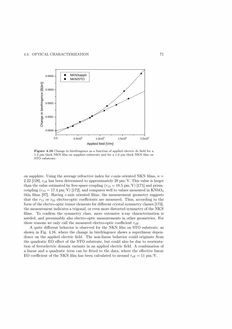
4.3. OPTICAL CHARACTERIZATION 71
0.0 5.0x10⁵ 1.0x10⁶ 1.5x10⁶ 2.0x10⁶
0.0000
0.0001
0.0002
0.0003
0.0004
Cha
nge
in b
irefr
inge
nce
[δ(∆
n)]
Applied field [V/m]
NKN/sapph NKN/STO
Figure 4.16 Change in birefringence as a function of applied electric dc field for a1.3 µm thick NKN film on sapphire substrate and for a 1.0 µm thick NKN film onSTO substrate.
on sapphire. Using the average refractive index for c-axis oriented NKN films, n =2.22 [128], reff has been determined to approximately 28 pm/V. This value is largerthan the value estimated by free-space coupling (r13 = 18.5 pm/V) [171] and prism-coupling (r13 = 17.4 pm/V) [172], and compares well to values measured in KNbO3
thin films [97]. Having c-axis oriented films, the measurement geometry suggeststhat the r11 or r22 electro-optic coefficients are measured. Thus, according to theform of the electro-optic tensor elements for different crystal symmetry classes [173],the measurement indicates a trigonal, or even more distorted symmetry of the NKNfilms. To confirm the symmetry class, more extensive x-ray characterization isneeded, and presumably also electro-optic measurements in other geometries. Forthese reasons we only call the measured electro-optic coefficient reff .
A quite different behavior is observed for the NKN film on STO substrate, asshown in Fig. 4.16, where the change in birefringence shows a superlinear depen-dence on the applied electric field. The non-linear behavior could originate fromthe quadratic EO effect of the STO substrate, but could also be due to reorienta-tion of ferroelectric domain variants in an applied electric field. A combination ofa linear and a quadratic term can be fitted to the data, where the effective linearEO coefficient of the NKN film has been calculated to around reff = 11 pm/V.

Chapter 5
Summary of Results and Outlook
In this chapter, I will summarize the results in the included publications and man-uscripts, as well as discussing ideas for future research.
5.1 Structural and Electrical Properties of Na0.5K0.5NbO3
A major part of this thesis work has been devoted to characterization of structuraland electrical properties of the Na0.5K0.5NbO3 (NKN) films.
5.1.1 Growth and crystallographic characteristics Na0.5K0.5NbO3 films
In this thesis, Na0.5K0.5NbO3 films have mainly been grown by rf magnetron sput-tering with thicknesses ranging from some hundred nanometers to around 2.0 µmusing single-phase, high-density ceramic targets. Several single-crystal oxide sub-strates have been explored, including LaAlO3 (Papers I, II, and IV), r-cut sapphire(Papers III–VII), Nd:YAlO3 (Paper V), and SrTiO3 (Paper VII). On perovskiteLaAlO3 (001) and SrTiO3 (001) epitaxial cube-on-cube growth of NKN films withnarrow full width at half maximum (FWHM) in rocking curve of NKN(001) (downto 0.60) has been confirmed by x-ray diffraction (XRD). NKN films with thicknessup to 2.0 µm have been deposited without cracking. NKN films on Nd:YAlO3(001)exhibit strongly polar axis orientation, with FWHM of rocking curve around 1.8.However, for this substrate growth parameters were not optimized in detail, so bet-ter performance could be expected. A great deal of attention has been addressedto NKN films on Al2O3 substrates. Sapphire was chosen as substrate due to itsextended use in microelectronics in general and optoelectronics in particular. Sap-phire has a pseudo-hexagonal structure, where an r-cut substrate has a reasonablelattice match with perovskite NKN. Pure perovskite phase films with thicknessesup to 2.0 µm have been grown, showing preferentially polar axis orientation. Therelative intensity between NKN(001) and NKN(110) diffraction peaks has been cal-culated to I001/I110 > 260, compared to 0.67 for the NKN ceramic target. FWHM
73

74 CHAPTER 5. SUMMARY OF RESULTS AND OUTLOOK
of the NKN(001) peak has been measured to as low as 1.6. NKN films havealso been deposited on conductive polycrystalline Pt80Ir20 substrates (Paper II),showing pure perovskite phase.
5.1.2 AFM characterization
The surface morphology of NKN films has been characterized for various substratesand thicknesses (Papers III–V,VII). Films on LaAlO3 and SrTiO3 substrates werevery smooth, with rms roughness between 1 and 2 nm for thicknesses up to 1.5 µm,which is on the order of what is needed for waveguide applications [50]. Films onsapphire show a more complicated behavior. Generally, the rms roughness increaseswith thickness (Paper IV), but there is also a tendency that films grown at condi-tions optimized for large I001/I110 ratio show larger rms roughness. Thus there is atrade-off in growing smooth films for waveguiding applications and growing highlypreferentially oriented films for electro-optic applications.
5.1.3 Electrical characterization
Most of the electrical characterization is presented in Papers I and II. The ferro-electric state in NKN/PtIr films at room temperature has been confirmed by po-larization loops with saturated polarization as high as 33.4 µC/cm2 at 700 kV/cm,remnant polarization of approximately 10 µC/cm2 and coercive field 90 kV/cm. Incomparison, the NKN/LAO planar structure, where the ferroelectric hysteresis ismeasured in the hard (in-plane) direction, has shown lower saturated polarization23.6 µC/cm2, lower remnant polarization around 2 µC/cm2 and lower coercive field36 kV/cm. The two different structures showed similar properties regarding low fre-quency dispersion (∆εr/εr = 9.8 % for NKN on PtIr and ∆εr/εr = 9.0 % for NKNon LAO between 1 kHz and 1 MHz), relatively low dissipation factor (tan δ ≃ 0.010)and dielectric permittivity up to εr = 500 at 1 MHz. The tunability of capacitancebetween zero field and 200 kV/cm has been calculated to 42.2 % and 17.5 % forthe vertical capacitor and the interdigital capacitor (IDC), respectively. The highervalue for the vertical structure was expected because of difference in film thicknessand capacitor geometry. The IDCs showed very good insulating properties withleakage current density on the order of 30 nA/cm2 at 400 kV/cm and dc resistivityρ = 2.1 × 10¹³ Ωcm. The resistivity was two orders of magnitude higher for theIDC structure. This difference can be explained by the defects within the film. Inthe vertical structure the electric field is applied in the direction of film growth,whereas the IDC has the field applied perpendicular to the growth direction. Webelieve that the main transport of leakage current occurs along the intergranulargrain boundaries, and thus is more pronounced in the vertical configuration.

5.2. OPTICAL AND WAVEGUIDING PROPERTIES OF NA0.5K0.5NBO3 75
5.2 Optical and Waveguiding Properties of Na0.5K0.5NbO3
Optical and waveguiding properties using the prism-coupling technique were ex-plored in Papers III–VI. In Paper III, bright-line spectra of up to 2.0 µm thickNKN waveguides on sapphire substrate exhibited sharp and distinguishable trans-verse magnetic and electric propagation modes, from which refractive index and filmthickness were calculated using a least mean square fit. The ordinary and extraordi-nary refractive indices were calculated to no = 2.247±0.002 and ne = 2.216±0.002for a 2.0 µm thick NKN film at λ = 632.8 nm. This implies a birefringence∆n = ne−no = −0.031±0.003 in the film. In Paper IV, waveguiding was reported inNKN/LAO structures. The birefringence was determined to ∆n = −0.054± 0.002,which is larger than the birefringence for NKN/sapphire. This can be attributedto the epitaxial quality observed by XRD for NKN/LAO. Other crystallite ori-entations will reduce the value of ∆n. In Paper V, dark-line spectra in trans-verse magnetic (TM) and transverse electric (TE) polarized light were reported atthree different wavelengths, including infrared optical communication wavelengths,λ = 1319 nm and λ = 1549 nm, for both NKN/Al2O3 and NKN on Nd:YAlO3
waveguides. Sharp dips corresponding to waveguide propagation modes in the thinfilm layers where observed for both substrates, implying Na0.5K0.5NbO3 as a fea-sible waveguiding material for integrated optical applications. The dispersion ofthe ordinary refractive index in Na0.5K0.5NbO3 is plotted in Paper VI, where it isshown to approximately follow the one-term Sellmeier expression.
5.3 Electro-optic Effect in Na0.5K0.5NbO3
In Papers VI and VII, investigation of the electro-optic (EO) effect measured intransmission of NKN films was reported. The thin films were coated with coplanarsurface electrodes, with dimensions 2.0 × 2.0 mm2 separated by a 10 µm widespacing, aligned parallel to the [112] axis of the r-cut sapphire and aligned parallelto the cubic axis of the STO substrate. The effective linear EO response wasdetermined to reff = 28 pm/V for NKN/Al2O3 with an applied dc field up to18 kV/cm (Paper VI). A quite different behavior was observed for NKN films onSTO substrate, where the change in birefringence showed a superlinear dependenceon the applied electric field. The non-linear behavior could originate from thequadratic EO effect of the STO substrate, but could also be due to reorientationof ferroelectric domain variants in an applied electric field. A combination of alinear and a quadratic term was fitted to the data, where the effective linear EOcoefficient of the NKN film was calculated to around reff = 11 pm/V.
5.4 Outlook
Ferroelectric thin films are of great interest as a waveguiding electro-optic materialin integrated applications for optical communication, but so far no working inte-
76 CHAPTER 5. SUMMARY OF RESULTS AND OUTLOOK
grated EO modulator prototype on semiconductor substrates has been reported.The demand for high speed transfer of huge data volumes is increasing rapidly. Inparallel the requirement of lowering the production costs is becoming more andmore important, so the optoelectronics community is longing for a break-throughwhere the high-speed, low-loss integrated EO modulator is a key component.
This research has focused on evaluating the optical and electro-optical proper-ties of Na0.5K0.5NbO3 thin films. The choice of material was based on the attrac-tive functional properties of NKN ceramics (relatively low dielectric permittivity,high electromechanical coupling coefficient, high remnant polarization and Curietemperature), in combination with our group’s knowledge of depositing NKN thinfilms with high quality. As has been presented in this thesis, we have confirmedwaveguiding in visible light and in the infrared band around the optical communi-cation wavelengths, as well as measured the effective EO coefficient.
The electro-optic measurements in transverse geometry implies r11 and/or r22components in the electro-optic tensor. As a next step, it would be elucidating todetermine the actual crystal symmetry of NKN films in detail, e.g., using high reso-lution XRD in combination with EO measurements. A natural continuation of thiswork is to improve the NKN films regarding epitaxial quality and surface roughness,and in that way reduce the losses and at the same time have a large electro-opticcoefficient. A useful figure-of-merit would be the effective EO coefficient divided bythe optical absorption coefficient of the material ( reff
α ).Having produced good, low loss waveguiding films, the next step is fabrication of
rib waveguide structures for modulator applications on oxide substrates. The sim-plest approach would be a phase modulator, but more attractive a Mach-Zehndermodulator. This modulator should be parameterized regarding half-wave voltage(Vπ) and extinction ratio. Finally, the whole concept is to be realized on semicon-ductor substrates (Si, GaAs), which would involve oxide buffer layers to preventleakage of the optical wave into the substrate [5, 83,139].
We have also been thinking of combining electro-optic ferroelectric niobate filmswith magneto-optic iron garnet thin films. In our group, Dr. S. Kahl defended hisdissertation on magneto-optic photonic crystals [174], so it would be natural tofabricate a combination of these materials. Such composite waveguides will combinetwo effects which do not coexist naturally in a material. The magneto-optical effectthat occurs when the magnetization of the garnet film and the propagation of lightare parallel is called the Faraday effect : The magnetization introduces a circularoptical anisotropy in the garnet material. This leads to a rotation of the polarizationof linear polarized light by the angle of Faraday rotation [175], which in thin filmwaveguides corresponds to TE to TM mode conversion.
Also, NKN is promising as a lead-free biocompatible material, where severalinteresting medical applications might emerge in the future, including piezoelectricsensing and actuation.
In conclusion, we have explored ferroelectric Na0.5K0.5NbO3 films in the electri-cal and optical domain, and demonstrated it as an attractive material for integratedoptics applications.

Bibliography
[1] G. L. Li and P. K. L. Yu, Optical intensity modulators for digital andanalog applications, J. Lightwave Technol., 21(9), 2010–2030 (2003).
[2] C. Buchal and M. Siegert, The physics of modulators, Proc. Int. SchoolPhys., 369–396 (1999).
[3] L. Thylén, Integrated optics in LiNbO3: Recent developments in devices fortelecommunications, J. Lightwave Technol., 6(6), 847–861 (1988).
[4] A. Donaldson, Candidate materials and technologies for integrated optics:fast and efficient electro-optic modulation, J. Phys. D: Appl. Phys., 24, 785–802 (1991).
[5] Y. Liang, J. Kulik, T. C. Eschrich, R. Droopad, Z. Yu, and P. Ma-
niar, Hetero-epitaxy of perovskite oxides on GaAs(001) by molecular beamepitaxy, Appl. Phys. Lett., 85(7), 1217–1219 (2004).
[6] L. A. Knauss, K. S. Harshavardhan, H.-M. Christen, H. Y. Zhang,
X. H. He, Y. H. Shih, K. S. Grabowski, and D. L. Knies, Growthof nonlinear optical thin films of KTa1−xNbxO3 on GaAs by pulsed laserdeposition for integrated optics, Appl. Phys. Lett., 73(26), 3806–3808 (1998).
[7] T. E. Murphy, D. Chen, and J. D. Phillips, Electronic properties offerroelectric BaTiO3/MgO capacitors on GaAs, Appl. Phys. Lett., 85(15),3208–3210 (2004).
[8] Y. Wang, C. Ganpule, B. T. Liu, H. Li, K. Mori, B. Hill, M. Wut-
tig, R. Ramesh, J. Finder, Z. Yu, R. Droopad, and K. Eisenbeiser,Epitaxial ferroelectric Pb(Zr,Ti)O3 thin films on Si using SrTiO3 templatelayers, Appl. Phys. Lett., 80(1), 97–99 (2002).
[9] H. Nishihara, M. Haruna, and T. Suhara, Optical Integrated Circuits,Optical and Electro-optical Engineering Series (McGraw-Hill book company,1985), ISBN 0-07-046092-2.
77

78 BIBLIOGRAPHY
[10] H. A. Lu, L. A. Wills, B. W. Wessels, W. P. Lin, T. G. Zhang, G. K.
Wong, D. A. Neumayer, and T. J. Marks, Second-harmonic generationof poled BaTiO3 thin films, Appl. Phys. Lett., 62(12), 1314–1316 (1993).
[11] C.-A. Tsai, A. Y. Wu, W.-R. Liou, P.-Y. Tung, and M.-L. Yeh,The study of temperature dependence of second harmonic generation in leadlanthanum titanate thin film by corona poling, Jpn. J. Appl. Phys., 42(9A),5581–5589 (2003).
[12] D. E. Kotecki, J. D. Baniecki, H. Shen, R. B. Laibowitz, K. L.
Saenger, J. J. Lian, T. M. Shaw, S. D. Athavale, C. Cabral, Jr.,
P. R. Duncombe, M. Gutsche, G. Kunkel, Y.-J. Par, Y.-Y. Wang,
and R. Wise, (Ba,Sr)TiO3 dielectrics for future stacked-capacitor DRAM,IBM J. Res. Develop., 43(3), 367–382 (1999).
[13] R. Waser and A. Rüdiger, Ferroelectrics: Pushing towards the digitalstorage limit, Nature Materials, 3, 81–82 (2004).
[14] P. Muralt, Ferroelectric thin films for micro-sensors and actuators: a re-view, J. Micromech. Microeng., 10, 136–146 (2000).
[15] J.-H. Koh, Processing and Properties of Ferroelectric Ag(Ta,Nb)O3 ThinFilms, Ph.D. thesis, Kungl. Tekniska Högskolan, KTH (2002).
[16] T. Mitsui, I. Tatsuzaki, and E. Nakamura, An Introduction to thePhysics of Ferroelectrics, Ferroelectricity and related phenomena, vol. 1 (Gor-don and Breach Science Publishers, 1976), ISBN 0-677-30600-8.
[17] E. T. Jaynes, Ferroelectricity, Investigation in Physics (Princeton UniversityPress, 1953), ISBN 99-0991628-2.
[18] J. Valasek, Piezoelectric and allied phenomena in Rochelle salt, Phys. Rev.,15(6), 537–538 (1920).
[19] J. Valasek, Piezo-electric and allied phenomena in Rochelle salt, Phys. Rev.,17(4), 475–481 (1921).
[20] G. Busch and P. Scherrer, A new seignettoelectric substance, Naturwiss.,23, 737 (1935).
[21] M. E. Lines and A. M. Glass, Principles and Applications of Ferroelectricsand Related Materials (Clarendon Press, 1977), ISBN 0-19-851286-4.
[22] Y. Xu, Ferroelectric Materials and Their Applications (Elsevier Science Pub-lisher B.V., 1991), ISBN 0-444-88354-1.
[23] K. Uchino, Ferroelectric Devices, Materials Engineering, vol. 16 (MarcelDekker, 2000), ISBN 0-8247-8133-3.

79
[24] A. Ballato, Piezoelectricity: Old effect, new thrusts, IEEE T. Ultrason.Ferr., 42(5), 916–926 (1995).
[25] J. F. Tressler, S. Alkoy, and R. E. Newnham, Piezoelectric sensorsand sensor materials, J. Electroceram., 2(4), 257–272 (1998).
[26] J. S. Speck and W. Pompe, Domain configuration due to multiple misfitrelaxation mechanisms in epitaxial ferroelectric thin films. I. Theory, J. Appl.Phys., 76(1), 468–476 (1994).
[27] J. S. Speck, A. Seifert, W. Pompe, and R. Ramesh, Domain configura-tion due to multiple misfit relaxation mechanisms in epitaxial ferroelectric thinfilms. II. Experimental verification and implications, J. Appl. Phys., 76(1),477–483 (1994).
[28] W. J. Merz, Domain formation and domain wall motions in ferroelectricBaTiO3 single crystals, Phys. Rev., 95(3), 690–698 (1954).
[29] E. A. Little, Dynamic behavior of domain walls in barium titanate, Phys.Rev., 98(4), 978–984 (1955).
[30] G. Dolino, Direct observation of ferroelectric domains in TGS with second-harmonic light, Appl. Phys. Lett., 22(4), 123–124 (1973).
[31] J. H. Hooton and W. J. Merz, Etch patterns and ferroelectric domainsin BaTiO3 single crystals, Phys. Rev., 98(2), 409–413 (1955).
[32] R. C. Bradt and G. S. Ansell, Aging in tetragonal ferroelectric bariumtitanate, J. Am. Ceram. Soc., 52(4), 192–198 (1969).
[33] C. Bousquet, M. Lambert, A. M. Quittet, and A. Guinier, Étudepoint par point de la surface d’un cristal par des méthodes du type Berg-Barrett, Acta Cryst., 16, 989–993 (1963).
[34] G. L. Pearson and W. L. Feldman, Powder-pattern techniques for de-lineating ferroelectric domain structures, J. Phys. Chem. Solids, 9(1), 28–30(1959).
[35] J. Hatano, F. Suda, and H. Futama, Improved powder-pattern techniquefor delineating ferroelectric domains, Jpn. J. Appl. Phys., 12(10), 1644–1645(1973).
[36] Y. Furuhata and K. Toriyama, New liquid-crystal method for revealingferroelectric domains, Appl. Phys. Lett., 23(7), 361–362 (1973).
[37] L. M. Levinson, Electronic Ceramics: Properties, Configuration, and Appli-cations, Electrical Engineering and Electronics, vol. 44 (Marcel Dekker, 1988),ISBN 0-8247-7761-1.
80 BIBLIOGRAPHY
[38] A. Yariv and P. Yeh, Optical Waves in Crystals (John Wiley & Sons,1984), ISBN 0-471-09142-1.
[39] H. S. Nalwa, Nonlinear Optical Materials, Handbook of Advanced Electronicand Photonic Materials and Devices, vol. 9 (Academic Press, 2001), ISBN0-12-513759-1.
[40] M. Veithen, X. Gonze, and P. Ghosez, First-principles study of theelectro-optic effect in ferroelectric oxides, Phys. Rev. Lett., 93(18), 187401(2004).
[41] R. Waser, Nanoelectronics and Information Technology (Wiley-VCH Verlag,2003), ISBN 3-527-40363-9.
[42] P. K. Tien, Light waves in thin films and integrated optics, Appl. Optics,10(11), 2395–2413 (1971).
[43] L. L. Boyer, A. Y. Wu, G. W. Metzger, and J. R. McNeil, Propertiesof ion beam deposited Pb1−xLax(ZryTiz)1−x/4O3, J. Vac. Sci. Technol. A,7(3), 1199–1201 (1989).
[44] L. Xuan, S. Pan, Z. Chen, R. Wang, W. Shi, and C. Li, Second har-monic generation in BaTiO3 films doped with cerium, Appl. Phys. Lett.,73(20), 2896–2898 (1998).
[45] W. F. Zhang, M. S. Zhang, Z. Yin, Y. Z. Gu, Z. L. Du, and B. L.
Yu, Large third-order optical nonlinearity in SrBi2Ta2O9 thin films by pulsedlaser deposition, Appl. Phys. Lett., 75(7), 902–904 (1999).
[46] E. Cross, Lead-free at last, Nature, 432, 24–25 (2004).
[47] A. Ashkin, G. D. Boyd, J. M. Dziedzic, R. G. Smith, A. A. Ballman,
J. J. Levinstein, and K. Nassau, Optically-induced refractive index inho-mogeneities in LiNbO3 and LiTaO3, Appl. Phys. Lett., 9(1), 72–74 (1966).
[48] F. S. Chen, Optically induced change of refractive indices in LiNbO3 andLiTaO3, J. Appl. Phys., 40(8), 3389–3396 (1969).
[49] J. M. Mir and J. A. Agostinelli, Optical thin films for waveguide appli-cations, J. Vac. Sci. Technol. A, 12(4), 1439–1445 (1994).
[50] D. K. Fork, F. Armani-Leplingard, and J. J. Kingston, Optical lossesin ferroelectric oxide thin films: Is there light at the end of the tunnel?, MRSSymp. Proc., 361, 155–166 (1995).
[51] F. J. Walker, R. A. McKee, H.-W. Yen, and D. E. Zelmon, Opticalclarity and waveguide performance of thin film perovskites on MgO, Appl.Phys. Lett., 65(12), 1495–1497 (1994).

81
[52] H. H. Landolt and R. Börnstein, Numerical data and functional re-lationships in science and technology, Crystals and Solid State Physics, vol.III/16a: Ferroelectrics and Related Substances (Springer-Verlag, 1981), ISBN3-540-09880-1.
[53] H. H. Landolt and R. Börnstein, Numerical data and functional re-lationships in science and technology, Crystals and Solid State Physics, vol.III/28a: Ferroelectrics and Related Substances (Springer-Verlag, 1990), ISBN3-540-51127-X.
[54] C.-R. Cho, Ferroelectric Na0.5K0.5NbO3 Thin Films: Processing, PhysicalProperties and Applications, Ph.D. thesis, Kungl. Tekniska Högskolan, KTH(2001).
[55] H. S. Nalwa, Ferroelectric Polymers, Plastic Engineering, vol. 28 (MarcelDekker, 1995), ISBN 0-8247-9468-0.
[56] D. K. Das-Gupta, Ferroelectric Polymers and Ceramic-Polymer Compos-ites, Key Engineering Materials, vol. 92-93 (Trans Tech Publications Ltd,1994), ISBN 0-87849-674-2.
[57] M. DiDomenico, Jr. and S. H. Wemple, Oxygen-octahedra ferroelectrics.I. Theory of electro-optic and nonlinear optical effects, J. Appl. Phys., 40(2),720–734 (1969).
[58] S. H. Wemple and M. DiDomenico, Jr., Oxygen-octahedra ferroelectrics.II. Electro-optical and nonlinear-optical device applications, J. Appl. Phys.,40(2), 735–752 (1969).
[59] C. Chen and G. Liu, Recent advances in nonlinear optical and electro-optical materials, Ann. Rev. Mater. Sci., 16, 203–243 (1986).
[60] B. Jaffe, W. R. Cook, and H. Jaffe, Piezoelectric Ceramics (AcademicPress, 1990), ISBN 1878907107.
[61] E. R. Myers, B. A. Tuttle, S. B. Desu, and P. K. Larsen, FerroelectricThin Films III, MRS Symposium Proceedings, vol. 310 (Materials ResearchSociety, 1993), ISBN 1-55899-206-5.
[62] R. M. W. J. S. Speck, D. K. Fork and T. Shiosaki, Epitaxial OxideThin Films II, MRS Symposium Proceedings, vol. 401 (Materials ResearchSociety, 1996), ISBN 1-55899-304-5.
[63] M. P. Moret, M. A. C. Devillers, K. Wörhoff, and P. K. Larsen,Optical properties of PbTiO3, BaZrxTi1−xO3, and PbZrO3 films depositedby metalorganic chemical vapor on SrTiO3, J. Appl. Phys., 92(1), 468–474(2002).
82 BIBLIOGRAPHY
[64] C. E. Land, Longitudinal electrooptic effects and photosensitivities of leadzirconate titanate thin films, J. Am. Ceram. Soc., 72(11), 2059–2064 (1989).
[65] B. G. Potter, M. B. Sinclair, and D. Dimos, Electro-optical charac-terization of Pb(Zr,Ti)O3 thin films by waveguide refractometry, Appl. Phys.Lett., 63(16), 2180–2182 (1993).
[66] G. H. Haertling and C. E. Land, Hot-pressed (Pb,La)(Zr,Ti)O3 ferroelec-tric ceramics for electrooptic applications, J. Am. Ceram. Soc., 54(1), 1–11(1971).
[67] G. Haertling, PLZT electrooptic materials and applications – A review,Ferroelectrics, 75(1-2), 25–55 (1987).
[68] H. Adachi, T. Kawaguchi, K. Setsune, K. Ohji, and K. Wasa, Electro-optic effects of (Pb,La)(Zr,Ti)O3 thin films prepared by rf planar magnetronsputtering, Appl. Phys. Lett., 42(10), 867–868 (1983).
[69] H. Adachi, T. Mitsuyu, O. Yamazaki, and K. Wasa, Ferroelectric(Pb,La)(Zr,Ti)O3 epitaxial thin films on sapphire grown by rf-planar mag-netron sputtering, J. Appl. Phys., 86(2), 736–741 (1986).
[70] A. Mukherjee, S. R. J. Brueck, and A. Y. Wu, Electro-optic effects inthin-film lanthanum-doped lead zirconate titanate, Opt. Lett., 15(3), 151–153(1990).
[71] K. D. Preston and G. H. Haertling, Comparison of electro-optic lead-lanthanum zirconate titanate films on crystalline and glass substrates, Appl.Phys. Lett., 60(23), 2831–2833 (1992).
[72] G. Teowee, J. M. Boulton, and D. R. Uhlmann, Optical and electro-optical properties of sol-gel derived ferroelectric thin films, Integr. Ferroelectr.,20, 39–54 (1998).
[73] D. H. Reitze, E. Haton, R. Ramesh, S. Etemad, D. E. Leaird,
T. Sands, Z. Karim, and A. R. Tanguay, Electro-optic properties ofsingle crystalline ferroelectric thin films, Appl. Phys. Lett., 63(5), 596–598(1993).
[74] F. Wang, E. Furman, and G. H. Haertling, Electro-optic measurementsof thin-film materials by means of reflection differential ellipsometry, J. Appl.Phys., 78(1), 9–15 (1995).
[75] K. Nashimoto, PLZT thin film optical waveguide devices, Proc. 13th IEEEInt. Symp. on Applications of Ferroelectrics, 123–128 (2002).
[76] F. Wang, K. K. Li, V. Fuflyigin, H. Jiang, J. Zhao, P. Norris, and
D. Goldstein, Thin ferroelectric interferometer for spatial light modulations,Appl. Opt., 37(32), 7490–7495 (1998).

83
[77] M. Zgonik, P. Bernasconi, M. Duelli, R. Schlesser, P. Günter,
M. H. Garrett, D. Rytz, Y. Zhu, and X. Wu, Dielectric, elastic, piezo-electric, electro-optic, and elasto-optic tensors of BaTiO3 crystals, Phys. Rev.B, 50(9), 5941–5949 (1994).
[78] D. Kip, Photorefractive waveguides in oxide crystals: fabrication, propertiesand applications, Appl. Phys. B, 67(2), 131–150 (1998).
[79] D. M. Gill, B. A. Block, C. W. Conrad, B. W. Wessels, and S. T.
Ho, Thin film channel waveguides fabricated in metalorganic chemical va-por deposition grown BaTiO3 on MgO, Appl. Phys. Lett., 69(20), 2968–2970(1996).
[80] L. Beckers, J. Schubert, W. Zander, J. Ziesmann, A. Eckau,
P. Leinenbach, and C. Buchal, Structural and optical characterizationof epitaxial waveguiding BaTiO3 thin films on MgO, J. Appl. Phys., 83(6),3305–3310 (1998).
[81] R. A. McKee, F. J. Walker, J. R. Conner, E. D. Specht, and D. E.
Zelmon, Molecular beam epitaxy growth of epitaxial barium silicide, bar-ium oxide, and barium titanate on silicon, Appl. Phys. Lett., 59(7), 782–784(1991).
[82] T. E. Murphy, D. Chen, and J. D. Phillips, Integration of BaTiO3
ferroelectric thin films with GaAs for functional devices, Proc. 15th IEEEBien. U/G/I Microelect. Symp., 267–270 (2003).
[83] D. Chen, T. E. Murphy, S. Chakrabarti, and J. D. Phillips, Opti-cal waveguiding in BaTiO3/MgO/AlxOy/GaAs heterostructures, Appl. Phys.Lett., 85(22), 5206–5208 (2004).
[84] K. J. Choi, M. Biegalski, Y. L. Li, A. Sharan, J. Schubert,
R. Uecker, P. Reiche, Y. B. Chen, X. Q. Pan, V. Gopalan, L.-Q.
Chen, D. G. Schlom, and C. B. Eom, Enhancement of ferroelectricity instrained BaTiO3 thin films, Science, 306, 1005–1009 (2004).
[85] D. M. Gill, C. W. Conrad, G. Ford, B. W. Wessels, and S. T. Ho,Thin-film channel waveguide electro-optical modulator in epitaxial BaTiO3,Appl. Phys. Lett., 71(13), 1783–1785 (1997).
[86] A. Petraru, M. Siegert, M. Schmid, J. Schubert, and C. Buchal,Ferroelectric BaTiO3 thin film optical waveguide modulators, Mat. Res. Soc.Symp. Proc., 688, C8.1.1–C8.1.6 (2002).
[87] A. Petraru, J. Schubert, M. Schmid, and C. Buchal, FerroelectricBaTiO3 thin-film optical waveguide modulators, Appl. Phys. Lett., 81(8),1375–1377 (2002).

84 BIBLIOGRAPHY
[88] P. Tang, D. J. Towner, A. L. Meier, and B. W. Wessels, Low-voltage,polarization-insensitive, electro-optic modulator based on a polydomain bar-ium titanate thin film, Appl. Phys. Lett., 85(20), 4615–4617 (2004).
[89] P. Tang, D. J. Towner, A. L. Meier, and B. W. Wessels, Low-loss electrooptic BaTiO3 thin film waveguide modulator, IEEE Photonic Tech.Lett., 16(8), 1837–1839 (2004).
[90] P. Tang, D. J. Towner, A. L. Meier, and B. W. Wessels, Polarisation-insensitive Si3N4 strip-loaded BaTiO3 thin-film waveguide with low propaga-tion losses, Electron. Lett., 39(23), 1651–1652 (2003).
[91] P. Tang, D. J. Towner, T. Hamano, A. L. Meier, and B. W. Wes-
sels, Electrooptic modulation up to 40 GHz in a barium titanate thin filmwaveguide modulator, Opt. Express, 12(24), 5962–5967 (2004).
[92] T. M. Graettinger, S. H. Rou, M. S. Ameen, O. Auciello, and A. I.
Kingon, Electro-optic characterization of ion beam sputter-deposited KNbO3
thin films, Appl. Phys. Lett., 58(18), 1964–1966 (1991).
[93] A. F. Chow, D. J. Lichtenwalner, T. M. Graettinger, J. R. Busch,
O. Auciello, and A. I. Kingon, Microstructural and optical properties ofpotassium niobate thin films, Proc. 9th IEEE Symp. on Ferroelec., 794–796(1995).
[94] S. Schwyn Thöny, H. W. Lehmann, and P. Günter, Sputter depositionof epitaxial waveguiding KNbO3 thin films, Appl. Phys. Lett., 61(4), 373–375(1992).
[95] C. Zaldo, D. S. Gill, R. W. Eason, J. Mendiola, and P. J. Chan-
dler, Growth of KNbO3 thin films on MgO by pulsed laser deposition, Appl.Phys. Lett., 65(4), 502–504 (1994).
[96] M. J. Nystrom, B. W. Wessels, D. B. Studebaker, T. J. Marks,
W. P. Lin, and G. K. Wong, Epitaxial potassium niobate thin films pre-pared by metalorganic chemical vapor deposition, Appl. Phys. Lett., 67(3),365–367 (1995).
[97] B. H. Hoerman, B. M. Nichols, M. J. Nystrom, and B. W. Wessels,Dynamic response of the electro-optic effect in epitaxial KNbO3, Appl. Phys.Lett., 75(18), 2707–2709 (1999).
[98] B. H. Hoerman, B. M. Nichols, and B. W. Wessels, Dynamic responseof the dielectric and electro-optic properties of epitaxial ferroelectric thin films,Phys. Rev. B, 65, 224110 (2002).

85
[99] B. H. Hoerman, B. M. Nichols, and B. W. Wessels, The electro-opticproperties of epitaxial KTaxNb1−xO3 thin films, Opt. Commun., 219, 377–382(2003).
[100] K. Fujiura and K. Nakamura, KTN crystal with a large electro-opticeffect and the potential for improving optical device performance, Proc. 2004IEEE Int. Top. Meet. Microw. Phot. (2004).
[101] S. Toyoda, K. Fujiura, M. Sasaura, K. Enbutsu, A. Tate,
M. Shimokozono, H. Fushimi, T. Imai, K. Manabe, T. Matsuura,
T. Kurihara, S. C. J. Lee, and H. de Waardt, KTN-crystal-waveguide-based electro-optic phase modulator with high performance index, Electron.Lett., 40(13) (2004), doi:10.1049/el:20040518.
[102] S. Toyoda, K. Fujiura, M. Sasaura, K. Enbutsu, A. Tate,
M. Shimokozono, H. Fushimi, T. Imai, K. Manabe, T. Matsuura,
and T. Kurihara, Low-driving-voltage electro-optic modulator with novelKTa1−xNbxO3 crystal waveguides, Jpn. J. Appl. Phys., 43(8B), 5862–5866(2004).
[103] M. Ahtee and A. M. Glaser, Phase transitions in sodium niobate-potassium niobate solid solutions, Ferroelectrics, 7(1-4), 93–95 (1974).
[104] M. Ahtee and A. W. Hewat, Structural phase-transitions in sodium-potassium niobate solid-solutions by neutron powder diffraction, Acta Cryst.,A34, 309–317 (1978).
[105] G. Shirane, R. Newnham, and R. Pepinsky, Dielectric properties andphase transitions of NaNbO3 and (Na,K)NbO3, Phys. Rev., 96(3), 581–588(1954).
[106] G. H. Haertling, Properties of hot-pressed ferroelectric alkali niobate ce-ramics, J. Am. Ceram. Soc., 50(6), 329–330 (1967).
[107] L. Egerton and D. M. Dillon, Piezoelectric and dielectric properties ofceramics in the system potassium-sodium niobate, J. Am. Ceram. Soc., 42(9),438–442 (1959).
[108] R. E. Jaeger and L. Egerton, Hot pressing of potassium-sodium niobates,J. Am. Ceram. Soc., 45(5), 209–213 (1962).
[109] V. J. Tennery and K. W. Hang, Thermal and x-ray diffraction studies ofthe NaNbO3-KNbO3 system, J. Appl. Phys., 39(10), 4749–4753 (1968).
[110] K. Nilsson, J. Lidman, K. Ljungström, and C. Kjellman, Biocompat-ible material for implants (1999), WO Patent 99/54266.

86 BIBLIOGRAPHY
[111] X. Wang, U. Helmersson, S. Olafsson, S. Rudner, L.-D. Wernlund,
and S. Gevorgian, Growth and field dependent dielectric properties of epi-taxial Na0.5K0.5NbO3 thin films, Appl. Phys. Lett., 73(7), 927–929 (1998).
[112] C.-R. Cho, J.-H. Koh, A. Grishin, S. Abadei, and S. Gevorgian,Na0.5K0.5NbO3/SiO2/Si thin films varactor, Appl. Phys. Lett., 76(13), 1761–1763 (2000).
[113] C.-R. Cho and A. Grishin, Background oxygen effects on pulsed laser de-posited Na0.5K0.5NbO3 films: From superparaelectric state to ferroelectricity,J. Appl. Phys., 87(9), 4439–4448 (2000).
[114] S. Abadei, S. Gevorgian, C.-R. Cho, A. Grishin, J. Andreasson,
and T. Lindbäck, DC field dependent properties of Na0.5K0.5NbO3/SiO2/Sistructures at millimeter-wave frequencies, Appl. Phys. Lett., 78(13), 1900–1902 (2001).
[115] S. Abadei, S. Gevorgian, C.-R. Cho, and A. Grishin, Low frequencyand microwave performances of laser-ablated epitaxial Na0.5K0.5NbO3 filmson high-resistivity SiO2/Si substrates, J. Appl. Phys., 91(4), 2267–2276(2002).
[116] M. Blomqvist, J.-H. Koh, S. Khartsev, A. Grishin, and J. Andréas-
son, High-performance epitaxial Na0.5K0.5NbO3 thin films by magnetron sput-tering, Appl. Phys. Lett., 81(2), 337–339 (2002).
[117] Z. G. Zhang, S. I. Khartsev, and A. M. Grishin, Ferroelectric propertiesof Na0.5K0.5NbO3 films at low temperatures, Integr. Ferroelectr., 67, 59–68(2004).
[118] V. Bobnar, J. Bernard, and M. Kosec, Relaxorlike dielectric propertiesand history-dependent effects in the lead-free K0.5Na0.5NbO3–SrTiO3 ceramicsystem, Appl. Phys. Lett., 85(6), 994–996 (2004).
[119] Y. Saito, H. Takao, T. Tani, T. Nonoyama, K. Takatori, T. Homma,
T. Nagaya, and M. Nakamura, Lead-free piezoelectrics, Nature, 432, 84–87 (2004).
[120] A. M. Margolin, Z. S. Surovyak, I. N. Zakharchenko, V. A.
Aleshin, L. K. Chernysheva, M. G. Radchenko, and V. P. Dudke-
vich, (K,Na)NbO3 ferroelectric films synthesized by cathode sputtering, Sov.Phys. Tech. Phys., 33(12), 1435–1438 (1989).
[121] X. Wang, S. Olafsson, L. D. Madsen, S. Rudner, I. P. Ivanov,
A. Grishin, and U. Helmersson, Growth and characterization ofNa0.5K0.5NbO3 thin films on polycrystalline Pt80Ir20 substrates, J. Mater.Res., 17(5), 1183–1191 (2002).

87
[122] V. M. Kugler, F. Söderlind, D. Music, U. Helmersson, J. Andreas-
son, and T. Lindbäck, Microstructure/dielectric property relationship oflow temperature synthesised (Na,K)NbOx thin films, J. Cryst. Growth, 262,322–326 (2004).
[123] C.-R. Cho and B.-M. Moon, (Na,K)NbO3 thin films using metal-organicchemical vapor deposition, Integr. Ferroelectr., 45, 39–48 (2002).
[124] C.-R. Cho and A. Grishin, Self-assembling ferroelectric Na0.5K0.5NbO3
thin films by pulsed-laser deposition, Appl. Phys. Lett., 75(2), 268–270 (1999).
[125] C.-R. Cho, J.-H. Koh, A. Grishin, S. Abadei, P. Petrov, and
S. Gevorgian, Thin Na0.5K0.5NbO3 films for varactor applications, Mat.Res. Soc. Proc., 623, 109–118 (2000).
[126] C.-R. Cho, I. Katardijev, M. Grishin, and A. Grishin, Na0.5K0.5NbO3
thin films for voltage controlled acoustoelectric device applications, Appl.Phys. Lett., 80(17), 3171–3173 (2002).
[127] M. Blomqvist, J.-H. Koh, S. I. Khartsev, and A. M. Grishin, Rf-magnetron sputtered ferroelectric (Na,K)NbO3 films, Proc. 13th IEEE Int.Symp. on Applications of Ferroelectrics, 195–198 (2002).
[128] M. Blomqvist, S. Khartsev, A. Grishin, A. Petraru, and
C. Buchal, Optical waveguiding in magnetron-sputtered Na0.5K0.5NbO3 thinfilms on sapphire substrates, Appl. Phys. Lett., 82(3), 439–441 (2003).
[129] M. Blomqvist, S. Khartsev, A. Grishin, and A. Petraru, Rf sputteredNa0.5K0.5NbO3 films on oxide substrates as optical waveguiding material, In-tegr. Ferroelectr., 54, 631–640 (2003).
[130] M. Blomqvist, S. Khartsev, and A. Grishin, Visible and IR lightwaveguiding in ferroelectric Na0.5K0.5NbO3 thin films, Integr. Ferroelectr.,69, 277–286 (2005).
[131] D.-W. Kim, S.-H. Lee, and T. W. Noh, Structural and nonlinear opticalproperties of epitaxial LiNbO3 films grown by pulsed laser deposition, Mater.Sci. Eng. B, 56, 251–255 (1998).
[132] G. Balestrino, S. Martellucci, P. G. Medaglia, G. Petrocelli,
A. Tebano, A. Tucciarone, F. Gelli, E. Giorgetti, S. Sottini, and
L. Tapfer, Epitaxial LiNbO3 thin films grown by pulsed laser deposition foroptical waveguides, Appl. Phys. Lett., 78(9), 1204–1206 (2001).
[133] X. Lansiaux, E. Dogheche, D. Rèmiens, M. Guilloux-viry, A. Per-
rin, and P. Ruterana, LiNbO3 thick films grown on sapphire by using amultistep sputtering process, J. Appl. Phys., 90(10), 5274–5277 (2001).

88 BIBLIOGRAPHY
[134] S. D. Cheng, X. Q. Han, C. H. Kam, Y. Zhou, Y. L. Lam, J. T. Oh,
X. W. Xu, and T. C. Chong, c-axis-textured LiNbO3 thin films on Si(111)substrates, Appl. Phys. A, 73(4), 511–514 (2001), doi:10.1007/s003390100802.
[135] D. K. Fork and G. B. Anderson, Epitaxial MgO on GaAs(111) as a bufferlayer for z-cut epitaxial lithium niobate, Appl. Phys. Lett., 63(8), 1029–1031(1993).
[136] S.-H. Lee, T. W. Noh, and J.-H. Lee, Control of epitaxial growth of pulsedlaser deposited LiNbO3 films and their electro-optic effects, Appl. Phys. Lett.,68(4), 472–474 (1996).
[137] P. Tayebati, D. Trivedi, and M. Tabat, Pulsed laser deposition ofSBN:75 thin films with electro-optic coefficient of 844 pm/V, Appl. Phys.Lett., 69(8), 1023–1025 (1996).
[138] M. J. Nystrom, B. W. Wessels, W. P. Lin, G. K. Wong, D. A. Neu-
mayer, and T. J. Marks, Nonlinear optical properties of textured strontiumbarium niobate thin films prepared by metalorganic chemical vapor deposition,Appl. Phys. Lett., 66(14), 1726–1728 (1995).
[139] S. B. Xiong, Z. M. Ye, X. Y. Chen, X. L. Guo, S. N. Zhu, Z. G. Liu,
C. Y. Lin, and Y. S. Jin, Ferroelectric SrxBa1−xNb2O6 optical waveguidingthin films on SiO2-coated Si(100) substrates, Appl. Phys. A, 67, 313–316(1998).
[140] W. H. Steier, A. Chen, S.-S. Lee, S. Garner, H. Zhang,
V. Chuyanov, L. R. Dalton, F. Wang, A. S. Ren, C. Zhang,
G. Todorova, A. Harper, H. R. Fetterman, D. Chen, A. Udupa,
D. Bhattacharya, and B. Tsap, Polymer electro-optic devices for inte-grated optics, Chem. Phys., 245, 487–506 (1999).
[141] V. Detan, Y. Lévy, M. Dumont, P. Robin, and E. Chastaing, Electro-optic properties of a ferroelectric polymer studied by attenuated total reflec-tion, Opt. Commun., 69, 379–383 (1989).
[142] W. Wang, D. Chen, H. R. Fetterman, Y. Shi, W. H. Steier, and
L. R. Dalton, Traveling wave electro-optic phase modulator using cross-linked nonlinear optical polymer, Appl. Phys. Lett., 65(8), 929–931 (1994).
[143] L. Zhang, F. Zhang, K. Cooper, Y. Wang, Y. Liu, and R. Claus,Electro-optic property measurement of electrostatically self-assembled ultra-thin films, Opt. Commun., 186, 135–141 (2000).
[144] D. S. Hermann, G. Scalia, C. Pitois, F. D. Marco, K. D’havé, G. Ab-
bate, M. Lindgren, and A. Hult, Novel passive polymer waveguides in-tegrated with electro-optically active ferroelectric liquid crystals, Opt. Eng.,40(10), 2188–2198 (2001).

89
[145] W. Shi, Y. J. Ding, X. Mu, X. Yin, and C. Fang, Electro-optic andelectromechanical properties of poled polymer thin films, Appl. Phys. Lett.,79(23), 3496–3751 (2001).
[146] J.-W. Kang, J.-J. Kim, and E. Kim, All-optical Mach-Zehnder modulatorusing a photochromic dye-doped polymer, Appl. Phys. Lett., 80(10), 1710–1712 (2002).
[147] Z. Liu, S. S. Sarkisov, M. J. Curley, A. Leyderman, and C. Lee,Thin film electro-optic modulator based on single crystal of N-(4-nitrophenyl)-(L)-prolinol (NPP) grown from melt by the modified Bridgeman method, Opt.Eng., 42(3), 803–812 (2003).
[148] W. Geis, R. Sinta, W. Mowers, S. J. Deneault, M. F. Marchant,
K. E. Krohn, S. J. Spector, D. R. Calawa, and T. M. Lyszczarz, Fab-rication of crystalline organic waveguides with an exceptionally large electro-optic coefficient, Appl. Phys. Lett., 84(19), 3729–3731 (2004).
[149] R. K. Swamy, S. P. Kutty, J. Titus, S. Khatavkar, and M. Thakur,Electroabsorption in single-crystal film of a second-order optical material,Appl. Phys. Lett., 85(18), 4025–4027 (2004).
[150] A. Facchetti, E. Annoni, L. Beverina, M. Morone, P. Zhu, T. J.
Marks, and G. A. Pagani, Very large electro-optic responses in H-bondedheteroaromatic films grown by physical vapour deposition, Nature Materials,3, 910–917 (2004).
[151] B. El-Kareh, Fundamentals of Semiconductor Processing Technologies(Kluwer Academic Publishers, 1995), ISBN 0-7923-9534-4.
[152] O. Auciello and J. Engemann, Multicomponent and Multilayered ThinFilms for Advanced Microtechnologies: Techniques, Fundamentals and De-vices (Kluwer Academic Publishers, 1993), ISBN 0-7923-2265-7.
[153] D. B. Chrisey and G. K. Hubler, Pulsed Laser Deposition of Thin Films(John Wiley & Sons, Inc., 1994), ISBN 0-471-59218-8.
[154] B. D. Cullity and S. R. Stock, Elements of X-Ray Diffraction (PrenticeHall, 2001), ISBN 0-201-61091-4.
[155] D. K. Schroder, Semiconductor Material and Device Characterization(John Wiley & Sons, Inc., 1998), ISBN 0-471-24139-3.
[156] K. Fenske and D. Misra, Dielectric materials at microwave frequencies,Appl. Microwave and Wireless, 12(10), 92–100 (2000).
[157] C. H. Mueller, R. R. Romanofsky, and F. A. Miranda, Ferroelectricthin film & broadband satellite systems, IEEE Potentials, 20(2), 36–39 (2001).

90 BIBLIOGRAPHY
[158] C. L. Chen, H. H. Feng, Z. Zhang, A. Brazdeikis, Z. J. Huang,
W. K. Chu, C. W. Chu, F. A. Mirandra, F. W. V. Keuls, R. R. Ro-
manofsky, and Y. Liou, Epitaxial ferroelectric Ba0.5Sr0.5TiO3 thin filmsfor room-temperature tunable element applications, Appl. Phys. Lett., 75(3),412–414 (1999).
[159] J. Im, O. Auciello, P. K. Baumann, S. K. Streiffer, D. Y. Kaufman,
and A. R. Krauss, Composition-control of magnetron-sputter-deposited(BaxSr1−x)Ti1+yO3+z thin films for voltage tunable devices, Appl. Phys.Lett., 76(5), 625–627 (2000).
[160] B. H. Park, Y. Gim, Y. Fan, Q. X. Jia, and P. Lu, High nonlinearity ofBa0.6Sr0.4TiO3 films heteroepitaxially grown on MgO substrates, Appl. Phys.Lett., 77(16), 2587–2589 (2000).
[161] X. Wang, U. Helmersson, L. D. Madsen, I. P. Ivanov, P. Münger,
S. Rudner, B. Hjörvarsson, and J.-E. Sundgren, Composition, struc-ture, and dielectric tunability of epitaxial SrTiO3 thin films grown by ra-dio frequency magnetron sputtering, J. Vac. Sci. Technol. A, 17(2), 564–570(1999).
[162] M. J. Lancaster, J. Powell, and A. Porch, Thin-film ferroelectricmicrowave devices, Supercond. Sci. Tech., 11, 1323–1334 (1998).
[163] S. S. Gevorgian, T. Martinsson, P. L. J. Linnér, and E. L. Koll-
berg, CAD models for multilayered substrate interdigital capacitors, IEEE T.Microw. Theory, 44(6), 896–904 (1996).
[164] T. Tamir, Guided-Wave Optoelectronics (Springer-Verlag, 1988), ISBN 0-387-18795-2.
[165] C. M. Foster, S.-K. Chan, H. L. M. Chang, R. P. Chiarello, T. J.
Zhang, J. Guo, and D. J. Lam, Electromagnetic modes and prism-filmcoupling in anisotropic planar waveguides of epitaxial (101) rutile thin films,J. Appl. Phys., 73(11), 7823–7830 (1993).
[166] P. K. Tien, R. Ulrich, and R. J. Martin, Modes of propagating lightwaves in thin deposited semiconductor films, Appl. Phys. Lett., 14(9), 291–294 (1969).
[167] S. Monneret, P. Huguet-Chantôme, and F. Flory, m-lines technique:prism coupling measurement and discussion of accuracy for homogeneouswaveguides, J. Opt. A, 2, 188–195 (2000).
[168] R. Ulrich and R. Torge, Measurement of thin film parameters with aprism coupler, Appl. Opt., 12(12), 2901–2908 (1973).

91
[169] M. Aillerie, N. Théofanous, and M. D. Fontana, Measurement ofthe electro-optic coefficients: description and comparison of the experimentaltechniques, Appl. Phys. B, 70(3), 317–334 (2000).
[170] R. C. Jones, A new calculus for the treatment of optical systems: I De-scription and discussion of the calculus, J. Opt. Soc. Am., 31(7), 488–493(1941).
[171] A. M. Grishin and S. I. Khartsev, Electro-optical properties ofNa0.5K0.5NbO3 film on Si by free-space coupling technique, Mat. Res. Soc.Symp. Proc., 817, L6.17.1–L6.17.5 (2004).
[172] S. I. Khartsev, M. A. Grishin, and A. M. Grishin, Characterizationof heteroepitaxial Na0.5K0.5NbO3/ La0.5Sr0.5CoO3 electro-optical cell, Appl.Phys. Lett., 86(6), 062901 (2005).
[173] A. Yariv, Optical Electronics / Optical Electronics in Modern Communica-tions (Saunders Collage Publishing / Oxford University Press, 1991 / 1997),ISBN 0-03-047444-2 / 0-19-510626-1.
[174] S. Kahl, Bismuth Iron Garnet Films for Magneto-optical Photonic Crystals,Ph.D. thesis, Kungl. Tekniska Högskolan, KTH (2004).
[175] S. Huard, Polarisation of Light (John Wiley & Sons, Inc., 1997), ISBN0-471-96536-7.


Papers

Paper I.
High-performance epitaxial Na0.5K0.5NbO3 thin films by magnetron sputtering
M. Blomqvist, J.-H. Koh, S. Khartsev, A. Grishin, and J. Andréasson,Appl. Phys. Lett., 81, 337 (2002).


Paper II.
Rf-magnetron sputtered ferroelectric (Na,K)NbO3
M. Blomqvist, J.-H. Koh, S. Khartsev, and A. Grishin,Proceedings of the 13th IEEE International Symposium on Applications of
Ferroelectrics, 195 (2002).


Paper III.
Optical waveguiding in magnetron-sputtered Na0.5K0.5NbO3 thin films on sapphiresubstrates
M. Blomqvist, S. Khartsev, A. Grishin, A. Petraru, and Ch. Buchal,Appl. Phys. Lett., 82, 439 (2003).


Paper IV.
Rf sputtered Na0.5K0.5NbO3 films on oxide substrates as optical waveguidingmaterial
M. Blomqvist, S. Khartsev, A. Grishin, and A. Petraru,Integr. Ferroelectr., 54, 631 (2003).


Paper V.
Visible and IR light waveguiding in ferroelectric Na0.5K0.5NbO3 thin films
M. Blomqvist, S. Khartsev, and A. Grishin,Integr. Ferroelectr., 69, 277 (2005).


Paper VI.
Electro-optic ferroelectric Na0.5K0.5NbO3 films
M. Blomqvist, S. Khartsev, and A. Grishin,To appear in IEEE Photon. Technol. Lett. (2005).

Paper VII.
Electro-optic effect in ferroelectric Na0.5K0.5NbO3 thin films on oxide substrates
M. Blomqvist, S. Khartsev, and A. Grishin,Submitted to Integr. Ferroelectr. (2005).