Polarity sensitive electro-optical response in liquid crystal devices due to ionic diffusion in WO 3...
11
Ionics 5 (1999) 275 Polarity Sensitive Electro-Optical Response in Liquid Crystal Devices Due to Ionic Diffusion in WO3 Thin Films G. Strangi a),*, N. Scaramuzza a), C. Versace a), E. Cazzanelli a), F. Simone b), A. Pennisi c) and R. Bartolino a) a)Dipartimento di Fisica, Universit~ della Calabria and Istituto Nazionale per la Fisica della Materia (INFM), Unit~ di Cosenza; 1-87036 Rende (Cosenza), Italy. b)Dipartimento di Fisica, Universith di Catania and INFM, Unith di Catania 1-95129 Catania, Italy. c)CNR and INFM, Unit?a di Catania, Corso Italia 57,I-95129 Catania, Italy. Abstract. The present work is aimed to a deeper understanding of the polarity sensitive electro- optical response observed in a liquid crystal cell with asymmetric insertion of a thin film of tungsten trioxide, deposited by r.f. sputtering on a transparent ITO substrate. After preliminary structural characterization of the films, the electro-optical response of the liquid crystal cells con- taining a WO 3 layer has been analyzed. The voltage thresholds of the Fr6dericksz transition are increased or decreased for the anodic or the cathodic charge of the tungsten trioxide film, respectively. In such a way a polarity-sensitive electro-optical response is generated, with the same frequency of the applied field. Impedance and cyclic voltammetry measurements have been performed on liquid crystal cells having WO3 films inserted as electrode, for as-deposited films as well as for annealed films at increasing temperatures. A strong decrease of the ionic current is ob- served in the cell where the film underwent the highest temperature treatment, above 300 ~ All the measurements suggest that a charge redistribution occurs for the hydrogen ions, always present in the films, during the intercalation-deintercalation processes induced by the applied voltage, and it is responsible for the changes of the effective electric field acting on the liquid crystal layer. 1. Introduction Tungsten trioxide (WO3) is among the most studied materials for active electrochromic electrodes, because of its properties of good ionic conductivity for small cations (H +, Li § Na +) coupled with a reasonable electronic con- ductivity [1-7] and a remarkable change in the electronic band structure and consequently in the optical trans- mission spectrum, when cations are intercalated. Many applications have been studied, like hydrogen sensors [8], energy and light control system in buildings and vehicles, information display panels and others [7, 9]. In principle, the reversible intercalation-deintercalation processes of small ions occur in WO3 bulk crystals. It shows a very complex polymorphism [ 10-14], strongly dependent also *) Author for correspondence: E-mail: [email protected] on electronic impurities, grain size distribution, thermal and mechanical history [15], but all the various phases can be considered as successive deformations, associated to phonon condensation [16], of a simple cubic structure of ReO 3 type, based on corner-sharing octahedral units WO6; the guest cations can enter in available interstitial sites between such octahedra. On the other hand, the high efficiency of intercalation for small ions, needed for practical applications, has been achieved in thin films [17, 18] deposited by using several different techniques [19-23] like r.f. magnetron sputtering, evaporation, sol-gel synthesis. In these films the basic units are still the WO6 octahedra, but they can be arranged in disordered configurations of three-, four- and six-mem- bered rings, leaving many empty spaces [24, 25], appre-
-
Upload
independent -
Category
Documents
-
view
0 -
download
0
Transcript of Polarity sensitive electro-optical response in liquid crystal devices due to ionic diffusion in WO 3...

Ionics 5 (1999) 275
Polarity Sensitive Electro-Optical Response in Liquid Crystal Devices Due to Ionic Diffusion in WO3 Thin Films
G. Strangi a),*, N. Scaramuzza a), C. Versace a), E. Cazzanelli a), F. Simone b), A. Pennisi c) and R. Bartolino a)
a)Dipartimento di Fisica, Universit~ della Calabria and Istituto Nazionale per la Fisica della Materia (INFM),
Unit~ di Cosenza; 1-87036 Rende (Cosenza), Italy.
b)Dipartimento di Fisica, Universith di Catania and INFM, Unith di Catania 1-95129 Catania, Italy.
c)CNR and INFM, Unit?a di Catania, Corso Italia 57,I-95129 Catania, Italy.
Abstract. The present work is aimed to a deeper understanding of the polarity sensitive electro-
optical response observed in a liquid crystal cell with asymmetric insertion of a thin film of
tungsten trioxide, deposited by r.f. sputtering on a transparent ITO substrate. After preliminary
structural characterization of the films, the electro-optical response of the liquid crystal cells con-
taining a WO 3 layer has been analyzed. The voltage thresholds of the Fr6dericksz transition are
increased or decreased for the anodic or the cathodic charge of the tungsten trioxide film,
respectively. In such a way a polarity-sensitive electro-optical response is generated, with the same
frequency of the applied field. Impedance and cyclic voltammetry measurements have been
performed on liquid crystal cells having WO3 films inserted as electrode, for as-deposited films as
well as for annealed films at increasing temperatures. A strong decrease of the ionic current is ob-
served in the cell where the film underwent the highest temperature treatment, above 300 ~ All
the measurements suggest that a charge redistribution occurs for the hydrogen ions, always present
in the films, during the intercalation-deintercalation processes induced by the applied voltage, and it
is responsible for the changes of the effective electric field acting on the liquid crystal layer.
1. In troduc t ion Tungsten trioxide (WO3) is among the most studied
materials for active electrochromic electrodes, because of
its properties of good ionic conductivity for small cations
(H +, Li § Na +) coupled with a reasonable electronic con-
ductivity [1-7] and a remarkable change in the electronic
band structure and consequently in the optical trans-
mission spectrum, when cations are intercalated. Many
applications have been studied, like hydrogen sensors [8],
energy and light control system in buildings and vehicles,
information display panels and others [7, 9]. In principle,
the reversible intercalation-deintercalation processes of
small ions occur in WO3 bulk crystals. It shows a very
complex polymorphism [ 10-14], strongly dependent also
*) Author for correspondence: E-mail: [email protected]
on electronic impurities, grain size distribution, thermal
and mechanical history [15], but all the various phases
can be considered as successive deformations, associated to
phonon condensation [16], of a simple cubic structure of
ReO 3 type, based on corner-sharing octahedral units WO6;
the guest cations can enter in available interstitial sites
between such octahedra.
On the other hand, the high efficiency of intercalation
for small ions, needed for practical applications, has been
achieved in thin films [17, 18] deposited by using several
different techniques [19-23] like r.f. magnetron sputtering,
evaporation, sol-gel synthesis. In these films the basic
units are still the WO6 octahedra, but they can be arranged
in disordered configurations of three-, four- and six-mem-
bered rings, leaving many empty spaces [24, 25], appre-
276 Ionics 5 (1999)
ciably larger than the interstitial sites in the bulk crystal.
A refined study [26], aimed to model the radial distri-
bution function (RDF) given by X-ray measurements,
suggests a dominant six-membered rings configuration,
making these "amorphous" films quite similar to the
crystals with hexagonal symmetry. Obviously the real
symmetry is expected to depend on the deposition tech-
nique and on the specific parameters used during the film
preparation, but a preferred hexagonal distribution seems
to be frequent in the tungsten trioxide films. Another
ubiquitous character of these films is the presence of water
in remarkable amount. In fact, the open disordered struc-
ture allows for the intercalation of water molecules during
the process of film deposition, and this fact seems to be
correlated to the high values of proton conductivity [25,
27-29] and even'to Li + ion conductivity [30].
Moreover, the study of the stoichiometry of the de-
posited tungsten trioxide films reveals an uptake of the
water molecules during storage after film production
[31]:
WO3.0H0.3 + aH20 (1)
Ion beam analysis was used to investigate the presence of
hydrogen contained in the tungsten oxide films at different
times after production, obtaining significantly different
profiles [31 ]. This increase indicates that the film takes up
hydrogen-containing species during storage with a ratio
H/W = 0.3 three hours after production.
Dehydration reactions and structural transformations of
the films, strongly affecting the ionic conductivity, can be
obtained by thermal annealing [32, 33]. In general, high
temperature annealing of the WO 3 samples lead to a cry-
stalline structure belonging to the standard sequence [16]
derived from cubic ReO3 structure. The temperature value
necessary to this transition depends in some amount on
the bulk or thin film character of the sample and on the
deposition technique; its variations are reported between
300 ~ for evaporated films [32] and 500 ~ for films
prepared by the sol-gel process [22]. For lower tempe-
ratures intermediate steps are observed on the way toward
crystallization and structural collapse, in particular the
elimination of water molecules trapped in the film struc-
ture [32] . This process occurs over a wide range of
temperature, reflecting the different trapping potential for
such molecutes; in principle, the deposition methods and
the thermal history are relevant. For this reason, specific
structural, spectroscopic (IR and Raman) and electro-
chemical measurements are quite useful for any set of film
samples.
Beside the amorphous or crystalline structure, the sur-
face characters on a larger scale are very important to
determine the interactions of WO 3 thin films with mole-
cular compounds outside. The micromorphologic study of
the tungsten trioxide films shows the presence of a
columnar structure in which the inclination of the co-
lumns strongly depends on the deposition geometry [34].
This fact suggests that interesting effects would derive
from the combination of such kinds of oxide film surfaces
with a liquid crystal (LC) layer, following the specu-
lations proposed in previous works dealing with similar
oxides having columnar surface topography [34,35].
However, to our knowledge, no study has been made on
the static anchoring of LC molecules on tungsten oxide
films, and no device has been made to explore the
correlation between the properties of mixed ionic-
electronic conduction of the WO3 and the electro-optic
response with LC, before the experiments described in our
previous works [36, 37].
The aim of the present work is to explore the static
anchoring interaction of the nematic liquid crystal on the
sputtered thin film of WO3, as well as the interplay
between the electrochemistry of the ionic-electronic solid
conductor and the reorientational dynamics of the LC
layer. Therefore, the electrooptical response of several
cells has been studied in different ways. Beside the
standard measurements of the white light transmission
between crossed polarizers under the action of a square
wave applied voltage, more detailed investigations have
been made by using a specific experimental set-up for the
study of the Frtdericksz transition [38].
In addition, the impedances and the currents of the LC
cells containing WO3 have been investigated (complex
impedance plots and cyclic voltammetry). To highlight
the role of the WO3 film structure and the water content
on the electrochemical properties of the entire cell, a com-
parative investigation was carried out, including also cells
in which the WO3-coated electrodes were purposedly
annealed via heat-treatments at different temperatures.
2. Experimental Description 2.1. Sample Preparation. Thin WO 3 films were deposited
by r.f. sputtering in a reactive atmosphere of Ar and
02 gas. The flow rates were 1.2 scem for oxygen and 12
Ionics 5 (1999) 277
sccm for argon; the ratio oxygen/argon was maintained at
a value of 10% during deposition. Sputtering parameters
varied for the r.f. power between 100 and 250 W and for
the deposition times between 10 and 30 minutes, in order
to obtain a film thickness of some hundred nm. A cathode
target of 100 mm diameter was used; a distance of 80 mm
separates the target and the substrate, which consisted of
glass covered by an ITO (In203:Sn) conducting layer
(provided by Donnelly Corp.). The sheet resistance of ITO
layer was 20 D)Q. The samples were made using different
deposition times for tungsten trioxide to investigate the
influence of the film thickness on the electro-optical res-
ponse of the liquid crystal.
The heating treatment on the film used for LC cells
has been carried out in air, by using a standard laboratory
oven (Carbolite' Furnaces, Mod. RMF14/3). The sample
labeled A has been heated up to 260 ~ starting from
room temperature (RT), with a rate of 10 ~ up to
180 ~ and a slower rate, 5 ~ between 180 and 260
~ After 10 minutes at the maximum temperature, the
sample was cooled down with a rate of about 10 ~
to RT. The sample B was heated with a rate of 6-7
~ up to 250 ~ remained at such temperature for 15
minutes and underwent a further heating step up to 303 ~
with a rate of about 3 ~ After staying for 5 minutes
at the maximum temperature, the sample was cooled
down with the same rate of the former sample, 10
~
Both the electric and electro-optical characterizations of
the purposedly heat-treated glass plates coated by WO 3
have been carried out some days after the thermal anneal-
ing. In any case, they were kept in a sealed envelope
within a container filled with desiccant silica gel to avoid
water absorption.
The ITO transparent electrodes, without any surface
treatment to induce preliminary alignment of the liquid
crystal, were enclosed in the standard sandwich con-
figuration (see Fig. 1). The thickness of the cells was
ensured by stripes of Mylar (8-36 lxm). The introduction
of the liquid crystal in the space enclosed between the
asymmetric glass plates was made slowly to prevent any
orientational alignment induced by the flow. The nematic
liquid crystal inserted in the cell is known commercially
as BL001 by Merck (former E7); it is an eutectic mixture
of four different cyanobiphenyls compounds. The tem-
perature range of existence for the nematic mesophase is
extendeds from 20 ~ up to 61 ~ and the dielectric
anisotropy Ae = eli - e.L = + 13.8 (at 20 ~ being ell
and E.L the dielectric permittivities parallel and perpen-
dicular to the molecular director, respectively.
2.2. Experimental Measurements. The XRD characte-
rization of the sputtered film has been made by an x-ray
diffractometer Siemens D5000, using the Cu K-ct line,
and the electron diffraction pattern has been obtained by a
JEOL microscope. The Raman spectra have been collected"
by a Lab-Ram spectrometer with a confocal microscope
and a CCD detector. The exciting light was the 633 nm
line of a He-Ne laser, kept at low power (15 mW).
Observations of the electro-optical response of the
cells, between crossed polarizers, were made by a pola-
rizing microscope Axioskop Pol (Zeiss). Videomicro-
scopy was performed by a 3CCD color camera TCM 112
(GDS Elettronica) connected to a PC equipped to visualize
and to store the images of the samples.
The investigation of the transmitted light intensities
was carried out by a large area silicon photodiode (Hama-
matsu) mounted on the polarizing microscope. The photo-
current was collected by a digital oscilloscope (Tektronics,
Mod. TDS 784).
Moreover, to better characterize the polarity sensitive
effect, investigations were performed to examine the vol-
tage thresholds of the Frtdericksz transition. A special
equipment was arranged for this purpose (see Fig. 2), a
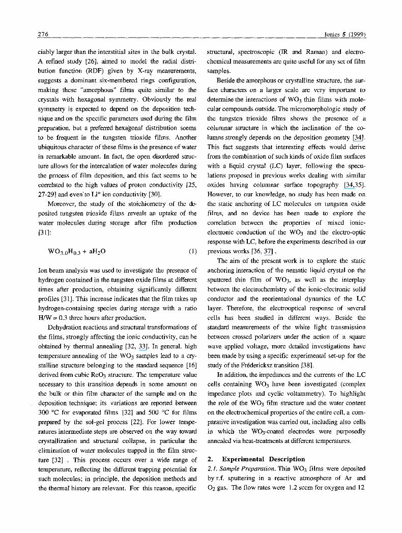
Fig. 1. Schematic drawing of the liquid crystal cell.
Fig. 2. Experimental set-up to study the Frtdericksz transition. L: He-Ne laser, P: polarizer, M: Mirror, O: Oven, S: Sample, A: Analyzer, PD: Photodiode, OA: Amplifier, WG: Waveform generator, DM: Digital multimeter, PC: computer.
278 Ionics 5 (1999)
polarized He-Ne laser beam was directed normal to the
boundary surfaces of the sample. The light transmitted
between crossed polarizers was detected by a silicon
photodiode and the signal was sent to a digital 3478A
multimeter (Hewlett Packard). An electric field, coming
from a waveform generator 8904A (Hewlett Packard) was
applied to the cell, perpendicular to the boundary glass
plates. Both waveform generator and digital multimeter
were connected to a PC.
For the comparative electrical measurements on liquid
crystal cells containing as-deposited and annealed elec-
trodes, glass plates coated by WO3 were chosen in such a
way to have sputtering parameters quite similar to each
other, so that chemical and structural characters are quite
comparable.
A preliminary electrochemical characterization of both
the as-deposited and the annealed samples was carried out
by a Potentiostat/Galvanostat/Impedance-meter EG&G
Mod. 273A.
The impedance of the samples was investigated in the
frequency range 1 mHz to 100 kHz. The amplitude of
the applied voltage was chosen to be 100 mV so to
avoid undesired electrically induced reorientation of the
liquid crystal.
Cyclic voltammetry measurements were also carried
out to complete the comparative analysis of the electro-
chemical behavior. The interval of the applied voltage was
-2 to 2 V and the scan rate was set to 50 mV/sec.
3. Resul ts and Discuss ion
3.1. WO 3 Films Characterization. The tungsten trioxide
films used in this work inside a LC cell have been
characterized with the usual techniques for structural de.
termination. Standard X-ray diffraction does not reveal any
crystalline symmetry in the as-deposited films, while
typical crystal patterns appear in XRD control measure-
ments made on the same films after high temperature
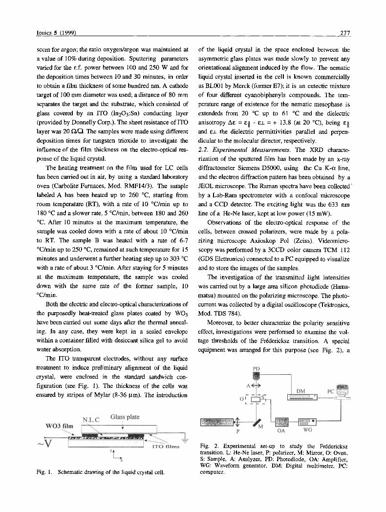
treatments (2 h at 400 ~ A different picture is given by
electron diffraction on the as-deposited films; as it can be
seen in Fig. 3, different regions of the same sample
generate hexagonal crystal-like diffraction patterns (Fig.
3a) or typical halos of amorphous structures (Fig. 3c). In
some region a coexistence of the two patterns is observed
(Fig. 3b). To get an additional information on the struc-
tural order in the films, some Raman measurements have
been carried out by using a confocal microscope. A com-
parison is possible between the as-deposited sample
Fig. 3. Electron diffraction patterns in different regions of a WO 3 film, as deposited, a) hexagonal pattern, b) mixed amorphous halos and cristalline diffraction spot, c) amor- phous halos
Ionics 5 (1999) 279
,=
_ . s ( a )
200 u I I I I I i j
400 600 800 1 00
Raman shift (cm -1)
(b) WO 3 annealed film
I I i I , i I
201 400 600 800 1000
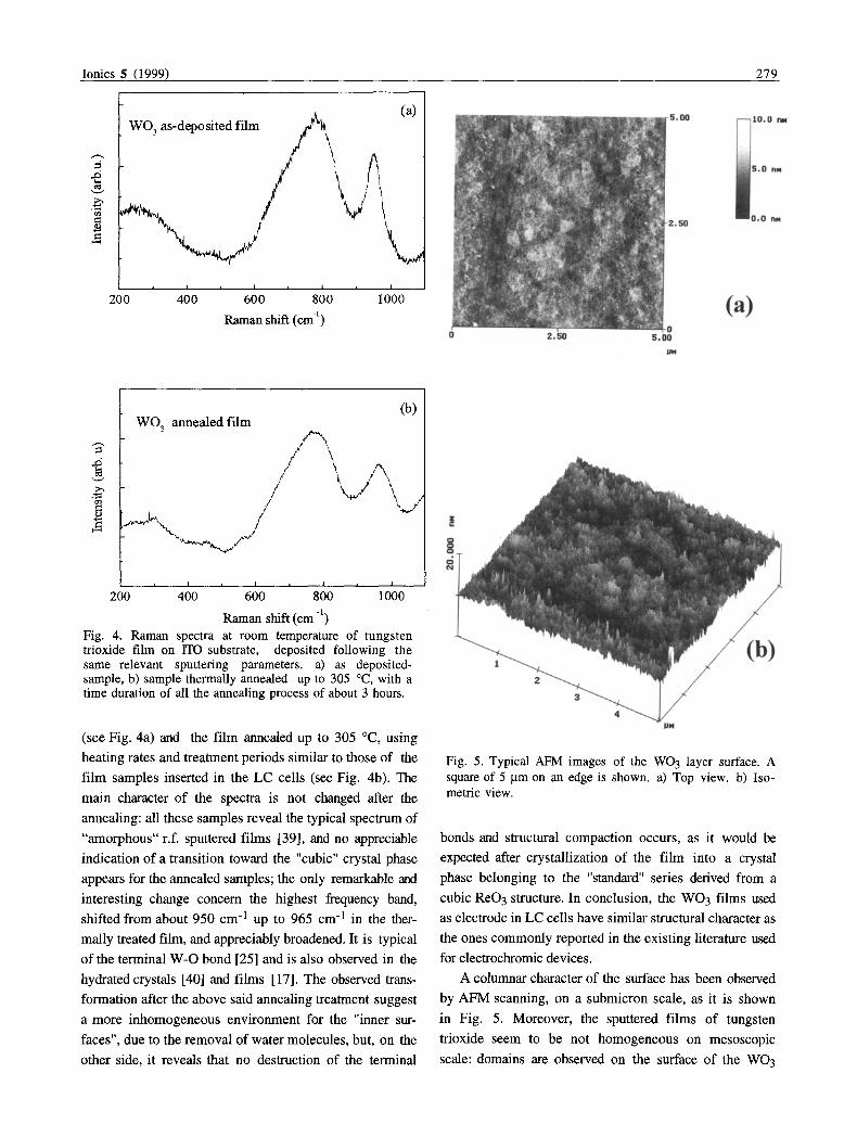
Raman shift (era -1) Fig. 4. Raman spectra at room temperature of tungsten trioxide film on ITO substrate, deposited following the same relevant sputtering parameters, a) as deposited- sample, b) sample thermally annealed up to 305 ~ with a time duration of all the annealing process of about 3 hours.
(see Fig. 4a) and the film annealed up to 305 ~ using
heating rates and treatment periods similar to those of the
film samples inserted in the LC cells (see Fig. 4b). The
main character of the spectra is not changed after the
annealing: all these samples reveal the typical spectrum of
"amorphous" r.f. sputtered films [39], and no appreciable
indication of a transition toward the "cubic" crystal phase
appears for the annealed samples; the only remarkable and
interesting change concern the highest frequency band,
shifted from about 950 cm -1 up to 965 cm -1 in the ther-
mally treated film, and appreciably broadened. It is typical
of the terminal W-O bond [25] and is also observed in the
hydrated crystals [40] and films [17]. The observed trans-
formation after the above said annealing treatment suggest
a more inhomogeneous environment for the "inner sur-
faces", due to the removal of water molecules, but, on the
other side, it reveals that no destruction of the terminal
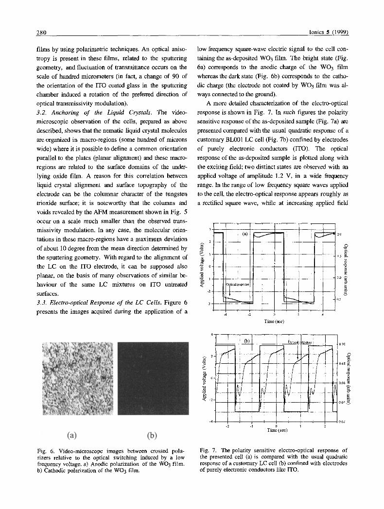
Fig. 5. Typical AFM images of the WO 3 layer surface. A square of 5 p.m on an edge is shown, a) Top view. b) Iso- metric view.
bonds and structural compaction occurs, as it would be
expected after crystallization of the film into a crystal
phase belonging to the "standard" series derived from a
cubic ReO3 structure. In conclusion, the WO3 films used
as electrode in LC cells have similar structural character as
the ones commonly reported in the existing literature used
for electrochromic devices.
A columnar character of the surface has been observed
by AFM scanning, on a submicron scale, as it is shown
in Fig. 5. Moreover, the sputtered films of tungsten
trioxide seem to be not homogeneous on mesoscopic
scale: domains are observed on the surface of the WO3
280 Ionics 5 (1999)
films by using polarimetric techniques. An optical aniso-
tropy is present in these films, related to the sputtering
geometry, and fluctuation of transmittance occurs on the
scale of hundred micrometers (in fact, a change of 90 of
the orientation of the ITO coated glass in the sputtering
chamber induced a rotation of the preferred direction of
optical transmissivity modulation).
3.2. Anchoring of the Liquid Crystals. The video-
microscopic observation of the cells, prepared as above
described, shows that the nematic liquid crystal molecules
are organized in macro-regions (some hundred of microns
wide) where it is possible to define a common orientation
parallel to the plates (planar alignment) and these macro-
regions are related to the surface domains of the under-
lying oxide film. A reason for this correlation between
liquid crystal alignment and surface topography of the
electrode can be the columnar character of the tungsten
trioxide surface; it is noteworthy that the columns and
voids revealed by the AFM measurement shown in Fig. 5
occur on a scale much smaller than the observed trans-
missivity modulation. In any case, the molecular orien-
tations in these macro-regions have a maximum deviation
of about 10 degree from the mean direction determined by
the sputtering geometry. With regard to the alignment of
the LC on the ITO electrode, it can be supposed also
planar, on the basis of many observations of similar be-
haviour of the same LC mixtures on ITO untreated
surfaces.
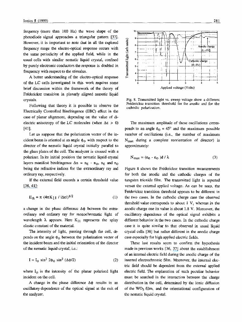
3.3. Electro-optical Response of the LC Cells. Figure 6
presents the images acquired during the application of a
low frequency square-wave electric signal to the cell con-
taining the as-deposited WO3 film. The bright state (Fig.
6a) corresponds to the anodic charge of the WO3 film
whereas the dark state (Fig. 6b) corresponds to the catho-
dic charge (the electrode not coated by WO 3 film was al-
ways connected to the ground).
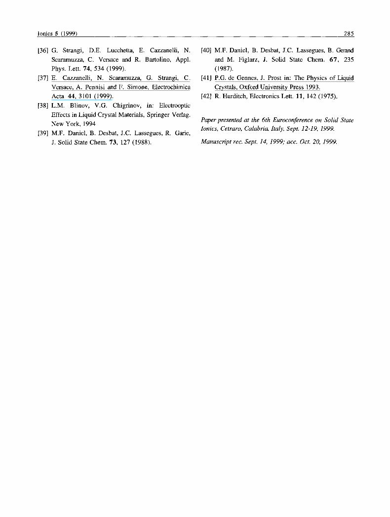
A more detailed characterization of the electro-optical
response is shown in Fig. 7. In such figures the polarity
sensitive response of the as-deposited sample (Fig. 7a) are
presented compared with the usual quadratic response of a
customary BL001 LC cell (Fig. 7b) confined by electrodes
of purely electronic conductors (ITO). The optical
response of the as-deposited sample is plotted along with
the exciting field; two distinct states are observed with an
applied voltage of amplitude 1.2 V, in a wide frequency
range. In the range of low frequency square waves applied
to the cell, the electro-optical response appears roughly as
a rectified square wave, while at increasing applied field
3 - m ( a )
2
| _ w
!i
.~ ]fical response
-2.
-3 �9 ~
-4 -2
E : I
0 2
Time (sec)
4 , ,
2--~"f : f ; ~ . . . . " 7 7 " ~ i r ' ,
l : ! j :t L,'~j,' t d . . . . . . . . . . . . . . . . . . . . t_. ...........
- 2 - i '
I
-4 t ; -2 -1 0 I
T i m e ( sec )
. . ~ 20
1.5
1.0
0.5
070 / "
068
0.66 ~
064
062
Fig. 6. Video-microscope images between crossed pola- rizers relative to the optical switching induced by a low frequency voltage, a) Anodic polarization of the WO 3 film. b) Cathodic polarization of the WO 3 film.
Fig. 7. The polarity sensitive electro-optical response of the presented cell (a) is compared with the usual quadratic response of a customary LC cell (b) confined with electrodes of purely electronic conductors like ITO.
Ionics 5 (1999) 281
frequency (more than 100 Hz) the wave shape of the
photodiode signal approaches a triangular pattern [37].
However, it is important to note that in all the explored
frequency range the electro-optical response occurs with
the same periodicity of the applied field, while in the
usual cells with similar nematic liquid crystal, confined
by purely electronic conductors the response is doubled in
frequency with respect to the stimulus.
A better understanding of the electro-optical response
of the LC cells investigated in this work requires some
brief discussion within the framework of the theory of
Fr&lericksz transition in planarly aligned nematic liquid
crystals.
Following that theory it is possible to observe the
Electrically Controlled Birefringence (EBC) effect in the
case of planar alignment, depending on the value of di-
electric anisotropy of the LC molecules (when Ae > 0)
[411.
Let us suppose that the polarization vector of the in-
cident beam is oriented at an angle (~o with respect to the
director of the nematic liquid crystal initially parallel to
the glass plates of the cell. The analyzer is crossed with a
polarizer. In its initial position the nematic liquid crystal
layers manifest birefringence An = n E - no, ne and no
being the refractive indices for the extraordinary ray and
ordinary ray, respectively.
If the external field exceeds a certain threshold value
[38, 41]:
Eth = rc (4~Kl l / IAEI) 1/2 (1)
a change in the phase difference A~) between the extra-
ordinary and ordinary ray for monochromatic light of
wavelength ~, appears. Here Kll represents the splay
elastic constant of the material.
The intensity of light, passing through the cell, de-
pends on the angle ~o between the polarization vector of
the incident beam and the initial orientation of the director
of the nematic liquid crystal, i.e.:
I = I o sin 2 2r sin 2 (AO/2) (2)
where I o is the intensity of the planar polarized light
incident on the cell.
A change in the phase difference A~ results in an
oscillatory dependence of the optical signal at the exit of
the analyzer.
1 0 - I
~ 7 -
6. "0
v :~ 5.
0 1
r "-x -I "--- 2SY ) ~,\il
f b ) S ,~ a~c charge
l ii �9 1
; I
2 3 4
Applied voltage (Volts)
Fig. 8. Transmitted light vs. sweep voltage show a different Frrdericksz transition threshold for the anodic and for the cathodic polarization.
The maximum amplitude of these oscillations corres-
ponds to an angle ~o = 45~ and the maximum possible
number of oscillations (i.e., the number of maximum
Nmax during a complete reorientation of director) is
approximately:
Nmax = (ne - no )d / ~ (3)
Figure 8 shows the Frrdericksz transition measurements
for both the anodic and the cathodic charges of the
tungsten trioxide film. The transmitted light is reported
versus the external applied voltage. As can be seen, the
Fredericksz transition threshold appears to be different in
the two cases. In the cathodic charge case the observed
threshold value corresponds to about 1 V, whereas in the
anodic charge one its value is about 1.8 V. Moreover, the
oscillatory dependence of the optical signal exhibits a
different behavior in the two cases. In the cathodic charge
case it is quite similar to that observed in usual liquid
crystal cells [38] but rather different in the anodic charge
case especially for high applied electric fields.
These last results seem to confirm the hypothesis
made in previous works [36, 37] about the establishment
of an internal electric field during the anodic charge of the
inserted electrochromic film. Moreover, the internal elec-
tric field should be dependent from the external applied
electric field. The explanation of such peculiar behavior
must be searched in the interaction between the charge
distribution in the cell, determined by the ionic diffusion
of the WO3 film, and the orientational configuration of
the nematic liquid crystal.

282 Ionics 5 (1999)
3.4. Electrical Measurements on the LC Cells. The 20M
established internal electric field can be associated to a
diffusion process of protons, coming from the amorphous
film and migrating toward the ITO electrode during the 1 ~M
anodic phase. To gain a deeper comprehension of the role
played by the adsorbed water molecules in the ionic ~ ~OM
conductivity of the protons, which are responsible of the •
polarity sensitive optical response, a comparative investi- 5O 0 Ok - - - -
gation has been carried out on several cells, in which one
of the glass plates was coated by a sputtered WO 3 thin
film having different structures or water content, as a con-
sequence of different heat treatments. Different experi-
mental techniques (complex impedance measurements and
cyclic voltammetry) have been used for such LC cells.
The thermal annealing of the arbitrarily chosen glasses
was carded out'to expel the adsorbed water molecules and
to study the electrochemical process at the boundary
surface of the LC cells, related to the established internal
electric field, depend on the hydrogen content of the films.
The analysis of the Nyquist diagrams (see Fig. 9) has
been performed both on the cells containing as-deposited
WO3 films (Fig. 9a) and in those with thermally annealed
tungsten oxide films (Figs. 9b and 9c); as it is pointed
out in the figures, the ionic diffusion process becomes
dominant in the plot for frequencies becoming more and
more lower, when passing from the cell with as-deposited 1400M-
film to the one containing annealed films. 120.OM . . . . .
The almost linear dependence between X = Im(Z) and
R = Re(Z) (Z being the impedance of the cell) indicates lOOOM-
that a diffusion process appears well defined in the former ~" 8OOM-
case (starting frequency is approximately 0.5 Hz), while ;K
in the latter cases, a more complex relationship between
X and R can be approximated to a straight line for a
lower frequency value, i.e. about 20 mHz. It is also
important to note that the diameters of the semicircle in
the Nyquist plots are quite different. In fact, the diameter
of the semicircle is related to the resistance of the cell and
it is remarkably increased in the cell labeled B (Fig. 9c).
The water molecules, desorbed after the heating of the
surface, do not contribute anymore to the diffusion
process of protons toward the liquid crystal layer; therefore
the observed behavior is quite reasonable.
But the picture becomes clearest analyzing the cyclic
voltammetry measurements performed on the same sam-
pies. Taking into account that the sweeping rate is main-
tained constant during all the measurements, the total
O0 O0
J iiiiii _i I
i I (a)
freq.= 0.5 H z "
500 Ok 10M
R(f2) 1 5M
IO.OM �9 - - - - - - ~ - -
0.0
0 .0 5 0 M IO.OM 15.0M 2 0 . 0 ~
RCf2)
60.OM -
40.OM -
20.OM -
O 0 A
0 .0
1
(c)
I
l r
F•e-l= 6 m H z
1. w v
; I i 20.OM ,40.OM 60.OM
T
W
I ,
80.0M 100.OM 120.OM
R(~)
2 0 M
25 .0M
140.0M
Fig. 9. Nyquist diagrams relative to the impedance mea- surement of the as deposited sample (a); sample A : maxi- mum annealing temperature T = 260 ~ (b); sample B: max. annealing temperature T = 305 ~ (c).
transferred charge is represented by the area enclosed in the
cycle.

Ionics 5 (1999) 283
150.0n
100 0
5O 0
r j -50.On
-100 On i
-150.0n
-2
(a)
J / /
Applied voltage(Volts)
transferred charge is considerably reduced. Therefore it is
evident that more relevant structural and chemical trans-
formations for the protonic conductivity occur between
260 ~ and 300 ~
This current analysis on the cells containing WO3
films undergoing different treatments support the hypo-
thesis that an important diffusive process in the as-
deposited film plays a specific role for the creation of an
interfacial double layer by charge separation. This charge
separation is responsible for the internal electric field
establishment which modifies unipolarly the effective
electric field acting on the LC layer.
150 On
100 On
50 On
o.o
-50 On
-100.On
-150.0n
-2 -1
/ Applied voltage (Volts)
lO0.On
50 On
0o
-50 On
(c)
f
-100 On -2 -1
Z
I
I
II Applied voltage (Volts)
Fig. 10. Cyclic voltammetry of the as-deposited sample (a); 260 ~ annealed sample A (b); 305 ~ annealed sample B (c).
By comparing the plot of the measurement relative to the
sample without heat-treatment (Fig. 10a) with that rela-
tive to the annealed sample (Fig. 10c), it appears well
evident that in the case of annealed film above 300 ~ the
4. Conclusions
The main result of the present work is the unusual po-
larity sensitive electro-optical response for a nematic
liquid crystal device. The innovation consists in the
asymmetric confinement of the liquid-crystalline material
by insertion of an amorphous tungsten trioxide film that
is covering one of the boundary surfaces. The inserted
film is a material with mixed conduction properties
(electronic and ionic). In fact a large series of studies
conducted on these materials reveals that some amount of
hydrogen-containing species enters these films during the
sputtering deposition or after deposition, because of the
exposition to wet air.
The analysis of the measurements reveals an important
electrochemical process associated to the presence of OH
and O1-/2 groups in WO 3 films exposed to wet air. More
precisely, during the anodic charge of the WO3 thin film a
H § diffusion process occurs [42]. The consequence of this
displacement of charge is a reverse internal electric field
which counteracts unipolarly the external perturbation; in
such a way a greater modulus of the external applied field
is needed to reach the Fredericksz transition threshold. On
the contrary for the cathodic charge the same applied
voltage is sufficient to trigger the optical switching.
The ionic conductivity properties of the inserted films
play an important role in the rectifying behavior of the
optical response of the LC cells, because of a diffusion-
controlled charge redistributionprocess, which is mainly
responsible of the asymmetric effective electric field.
Experiments on asymmetric cells containing thermally
annealed WO 3 films demonstrate that the important
process involved in the considered device is due to the
protons, whose conductivity is strongly enhanced by the
water content of the films.

284 Ionics 5 (1999)
Further studies are planned with regard to different
cationic species, having also different initial concentra-
tions with the aim to develop an original electrooptical
device.
5. Acknowledgements The authors would like to thank the firm ISA Italia for
kindly providing the LABRam spectrometer used for the
Raman measurements. Another special acknowledgement
is reserved to Cristina Armellini, of CEFSA-CNR at
Trento, for her assistance in the thermal treatment of the
films.
Finally, the authors are indebted to Prof. L. M. Blinov
for the fruitful discussion and the helpful suggestions.
The work has been carried out in the framework of the
ORCHIS TMR RESEARCH NETWORK (Contract
Number: ERBFMRXCT97-0119).
6. References [I] S.K. Deb, Appl. Optics Suppl. 3, 192 (1969); S.K.
Deb, Philos. Mag. 27, 801 (1973).
[2] M.J. Sienko and J.M. Berak, in: The Chemistry of
Extended Defects in Non-Metallic Solids, (L. Eyring
and M. O'Keeffe, eds.) North Holland, 1970.
[3] B.W. Faughnan, R.S. Crandal and P.M. Heyman,
RCA Rev. 36, 177 (1975).
[4] T. Hirose, J. Phys. Soc. Jpn. 49, 562 (1980). [5] J. Nagai, Solid State Ionics 40/41, 383 (1990).
[6] C.G. Granqvist, Solid State Ionics 53&56, 479
(1992).
C.G. Granqvist, Appl. Phys. A 57, 3 (1993).
D.J. Smith, J.F. Vetelino and R.S. Falconer, Sen-
sors and Actuators B 13, 264 (1993).
[9] Proc. III Symposium on "Electrochromic Materials",
(K.C. Ho, C.B. Greenberg and D.M. Mac Arthur,
eds.) proc. Vol. 96-24, The Electrochemical Society
(Pennington, NY, 1997).
[10] S. Tanisaki, J. Phys. Soc. Japan. 15, 566 (1960).
[11] B.O. Loopstra and P. Boldrini, Acta Crystallogr. B
21, 158 (1966); B.O. Loopstra and H.M. Rietveld,
Acta Crystallogr. B 25, 1420 (1969).
[12] E. Salje and K. Viswanathan, Acta Crystallogr. A
31, 356 (1975); E. Salje, Acta Crystallogr. B 33,
574 (1975).
[13] P.W. Woodward, A.W. Sleight and T. Vogt, J.
Phys. Chem. Solids 56, 1305 (1995).
[14] K.L. Kehl, R.G. Hay and D.J. Wahl, J. Appl. Phys.
23, 212 (1952).
.[7] [8]
[15] E. Cazzanelli, G. Mariotto, C. Vinegoni, A.
Kuzmin and J. Purans, J. Solid State Chemistry
143, 24 (1999).
[16] M. Kawaminami, and T. Hirose, J. Phys. Soc.
Japan. 46, 864 (1979).
[17] J.V. Gabrusenoks, P.D. Cikmach, A.R. Lusis, J.J.
Kleperis and G.M. Ramans, Solid State Ionics 14,
25 (1984).
[18] D. Dini, F. Decker, E. Masetti, J. Appl. Electro-
chemistry 26, 647 (1996).
[19] H. Demiryont, K.E. Nietering, Appl. Optics 28,
1494 (1989).
[20] O. Lev, Z. Wu, S. Bharathi, V. Glezer, A.
Modestov, J. Gun, L. Rahinovitch, S. Samphath,
Chem. Mater. 9, 2354 (1997).
[21] K. Marszalek, Thin Solid Films 175, 227 (1989).
[22] T. Nanba, T. Takahashi, T. Kudo, J. Non-Cryst.
Solids 178, 233 (1994).
[23] T. Nishide, F. Mizukami, Thin Solid Films 259,
212 (1995).
[24] P. Delichere, P. Falaras, M. Froment and A. Hugot
le Goff, Thin Solid Films 161, 35 (1988).
[25] T. Nanba, Y. Nishiyama and I. Yasui, J. Mater.
Res. 6, 1324 (1991).
[26] T. Nanba and I. Yasui, J. Solid State Chem. 83,
304 (1989).
[27] H.R. Zeller and H.U. Beyeler, Appl. Phys. 13, 231
(1977).
[28] J.A. Duffy, M.D. Ingram and P.M.S. Monk, Solid
State Ionics 58, 109 (1992).
[29] J. Vondr~k, J. Bludsk~t, Solid State Ionics 68, 317
(1994).
[30] C1. Bohnke, O. Bohnke, B. Carquille and G. Robert,
Solid State Ionics 6, 121 (1982).
[31] W Wagner, F. Rauch, C. Otterman and K. Bange,
Nuclear Instruments and Methods in Physics Re-
search B 68, 262 (1992).
[32] A. Agrawal, H. Habjbi, Thin solid Films 169, 257
(1989).
[33] M.D. Antonik, J.E. Schneider, E.L. Wittman, K.
Snow, J.F. Vetelino and R.J. Lad, Thin Solid Films
256, 247 (1995).
[34] T. Motohiro, Y. Taga, Thin Solid Films 185, 137
(1990).
[35] G.W. Mbise, D. Le Bellac, G.A. Niklasson, C.G.
Granqvist, J. Phys. D: Appl. Phys. 30, 2103
(1997).
Ionics 5 (1999) 285
[36] G. Strangi, D.E. Lucchetta, E. Cazzanelli, N.
Scaramuzza, C. Versace and R. Bartolino, Appl. Phys. Lett. 74, 534 (1999).
[37] E. Cazzanelli, N. Scaramuzza, G. Strangi, C. Versace, A. Pennisi and F. Simone, Electrochimica
Acta 44, 3101 (1999). [38] L.M. Blinov, V.G. Chigrinov, in: Electrooptic
Effects in Liquid Crystal Materials, Springer Verlag. New York, 1994
[39] M.F. Daniel, B. Desbat, J.C. Lassegues, R. Garie,
J. Solid State Chem. 73, 127 (1988).
[40] M.F. Daniel, B. Desbat, J.C. Lassegues, B. Gerand
and M. Figlarz, J. Solid State Chem. 67, 235 (1987).
[41] P.G. de Gennes, J. Prost in: The Physics of Liquid
Crystals, Oxford University Press 1993. [42] R. Hurditch, Electronics Lett. 11, 142 (1975).
Paper presented at the 6th Euroconference on Solid State Ionics, Cetraro, Calabria, Italy, Sept. 12-19, 1999.
Manuscript rec. Sept. 14, 1999; acc. Oct. 20, 1999.