Heavy-Metal-Free Solution-Processed Nanoparticle-Based Photodetectors: Doping of Intrinsic Vacancies...
9
Subscriber access provided by UNIV TORONTO ACS Nano is published by the American Chemical Society. 1155 Sixteenth Street N.W., Washington, DC 20036 Article Heavy-Metal-Free Solution-Processed Nanoparticle-Based Photodetectors: Doping of Intrinsic Vacancies Enables Engineering of Sensitivity and Speed Jiang Tang, Gerasimos Konstantatos, Sean Hinds, Stefan Myrskog, Andras G. Pattantyus-Abraham, Jason Clifford, and Edward H. Sargent ACS Nano, 2009, 3 (2), 331-338• DOI: 10.1021/nn800718u • Publication Date (Web): 31 December 2008 Downloaded from http://pubs.acs.org on March 25, 2009 More About This Article Additional resources and features associated with this article are available within the HTML version: • Supporting Information • Links to the 1 articles that cite this article, as of the time of this article download • Access to high resolution figures • Links to articles and content related to this article • Copyright permission to reproduce figures and/or text from this article
-
Upload
independent -
Category
Documents
-
view
3 -
download
0
Transcript of Heavy-Metal-Free Solution-Processed Nanoparticle-Based Photodetectors: Doping of Intrinsic Vacancies...

Subscriber access provided by UNIV TORONTO
ACS Nano is published by the American Chemical Society. 1155 Sixteenth StreetN.W., Washington, DC 20036
Article
Heavy-Metal-Free Solution-Processed Nanoparticle-BasedPhotodetectors: Doping of Intrinsic VacanciesEnables Engineering of Sensitivity and Speed
Jiang Tang, Gerasimos Konstantatos, Sean Hinds, Stefan Myrskog,Andras G. Pattantyus-Abraham, Jason Clifford, and Edward H. Sargent
ACS Nano, 2009, 3 (2), 331-338• DOI: 10.1021/nn800718u • Publication Date (Web): 31 December 2008
Downloaded from http://pubs.acs.org on March 25, 2009
More About This Article
Additional resources and features associated with this article are available within the HTML version:
• Supporting Information• Links to the 1 articles that cite this article, as of the time of this article download• Access to high resolution figures• Links to articles and content related to this article• Copyright permission to reproduce figures and/or text from this article

Heavy-Metal-Free Solution-ProcessedNanoparticle-Based Photodetectors:Doping of Intrinsic Vacancies EnablesEngineering of Sensitivity and SpeedJiang Tang,† Gerasimos Konstantatos,‡ Sean Hinds,‡ Stefan Myrskog,‡ Andras G. Pattantyus-Abraham,‡
Jason Clifford,‡ and Edward H. Sargent‡,*†Department of Materials Science and Engineering, 184 College Street, Toronto, Ontario M5S 3E4, and ‡Department of Electrical and Computer Engineering, University ofToronto, 10 King‘s College Road, Toronto, Ontario M5S 3G4, Canada
Digital imaging relies on arrays of in-dividually read photodetectors.High signal-to-noise imaging at
low light, combined with operation at video
frame rates, requires sensitivity and speed
simultaneously. In conventional photo-
diodes, in which the current collected is lim-
ited to one electron per photon incident,
external quantum efficiency (EQE) is used
as a proxy for sensitivity. Temporal response
may be quantified through the longest
time constant in a device’s rise or fall in re-
sponse to changes in illumination. EQEs ap-
proaching 100% (unity gain) are desired;
while temporal responses faster than 100
ms are desired for video frame-rate lag-free
imaging.
There is a growing interest1�6 in inte-
grating photosensitive layers on top of an
electronic read-out circuit instead of relying
on silicon’s own sensitivity.7 Whereas pho-
todiodes are restricted to unity EQE, photo-
conductive photodetectors provide gains of
10-fold and above, thus providing many
electrons for each photon incident. In con-
ventional silicon CMOS imaging, photo-
diodes are buried beneath multiple mi-
crometers of dielectric and metal
interconnect, and they typically occupy
less than half of the pixel area owing to
sharing of silicon area with read-out cir-
cuitry. In contrast, top-surface photodetec-
tors offer 100% fill factor.8 Silicon’s bandgap
limits its applications to the visible and
near-infrared, whereas the use of alterna-
tive top-surface photodetector materials
makes possible imaging from the UV9
through to the short-wavelength infrared.1
Promising recent reports of low-lag top-surface photoconductive photodetectorshaving the combination of good gain (�3)and acceptable temporal response (�100ms)10 have employed PbS colloidal quan-tum dots. More broadly, many recent ad-vances in colloidal quantum dotelectronics11,12 and optoelectronics13�15
have relied on the use of heavy-metal cat-ions such as Cd and Pb that raise concernsregarding toxicity and regulatoryacceptance.
Here we report Pb- and Cd-free photo-conductive photodetectors. Our materialsare based instead on indium sulfide (In2S3),a III2�VI3 semiconductor having a band gapof 2.03 eV.
As we report in detail below, employingthis much less familiar colloidal nanoparti-cle materials system raised significant
See the accompanying Perspective byNoone and Ginger on p 261.
*Address correspondence [email protected].
Received for review October 28, 2008and accepted December 15, 2008.
Published online December 31, 2008.10.1021/nn800718u CCC: $40.75
© 2009 American Chemical Society
ABSTRACT Photodetection in semiconductors enables digital imaging, spectroscopy, and optical
communications. Integration of solution-processed light-sensing materials with a range of substrates offers
access to new spectral regimes, the prospect of enhanced sensitivity, and compatibility with flexible electronics.
Photoconductive photodetectors based on solution-cast nanocrystals have shown tremendous progress in recent
years; however, high-performance reports to date have employed Pb- and Cd-containing materials. Here we report
a high-sensitivity (photon-to-electron gain >40), high-speed (video-frame-rate-compatible) photoconductive
photodetector based on In2S3. Only by decreasing the energetic depth of hole traps associated with intrinsic
vacancies in beta-phase In2S3 were we able to achieve this needed combination of sensitivity and speed. Our
incorporation of Cu� cations into beta-In2S3’s spinel vacancies that led to acceptable temporal response in the
devices showcases the practicality of incorporating dopants into nanoparticles. The devices are stable in air and
under heating to 215 °C, advantages rooted in the reliance on the stable inclusion of dopants into available sites
instead of surface oxide species.
KEYWORDS: indium sulfide · doping · intrinsic vacancy ·solution-processed · photoconductive · photodetector
ARTIC
LE
www.acsnano.org VOL. 3 ▪ NO. 2 ▪ 331–338 ▪ 2009 331

challenges in making a photoconductive photodetec-
tor having attractive performance. Specifically, long-
lived trap states, traceable to cationic vacancies associ-
ated with unoccupied indium tetrahedral positions in
In2S3’s defect spinel structure (beta phase),16 produced
unacceptably long temporal responses in our first gen-
eration of devices.
In response we searched for a means of filling these
vacant sites using metal ions. We found that the use of
Cu cations allowed us to engineer the trap state lifetime
to enable a desirable gain without the deleterious ef-
fects of excess lag. We note that these findings on dop-
ing overcome a longstanding problem in the colloidal
nanocrystal field: self-purification, a consequence of the
fact that the impurity solubility in small nanocrystals is
much lower than in bulk materials.17,18 We hypothesized
that we could overcome such difficulties in achieving
stable net doping by working with a material having in-
trinsic vacancies that would readily incorporate impuri-
ties if the size of impurity ion was compatible with the
volume of vacancy; and if the affinity of the impurity
ion was properly chosen.
As a consequence, we report herein a sensitive (R
� 10 A/W) and fast (� � 0.1 s) solution-processed vis-
ible photodetector based on Cu�-doped In2S3 nano-
plates. We initially produced visible photodetectors,
based on In2S3 nanoplates, having high responsivity
but slow temporal re-sponse. Then we devel-oped a one-pot postdop-ing strategy to introduceCu� into In2S3 nanoplatesin solution. Careful charac-terization of these materialsconfirmed the success ofCu� doping. An optimallevel of Cu� doping greatlyimproved photodetectorspeed with little sacrifice ofresponsivity. These deviceshold promise for high-sensitivity, video-frame-rate visible photodetectorapplications.
RESULTSWe first synthesized un-
doped In2S3 nanoplatesand characterized the per-formance of devices madefrom such materials. In2S3
nanoplates were synthe-sized by heating InCl3 andsulfur powder in oley-lamine at 215 °C using apreviously reported proto-col.19 As shown in Figure
1A, monodisperse In2S3 nanoplates were produced.The crystalline plates exhibit 6-fold symmetry with di-mensions in the plane on the order of 30 nm. After syn-thesis and isolation, solution ligand exchange was em-ployed to replace long oleylamine (�2.4 nm) with shortbutylamine (�0.6 nm) with the goal of increasingcharge carrier mobility by reducing interparticle spac-ing. We used Fourier transform infrared spectroscopy(FTIR) to evaluate the effectiveness of this ligand ex-change strategy. FTIR peaks (Figure 1b) of particular in-terest are the asymmetric and symmetric C�H stretch-ing vibration of a CH2 group at 2930 and 2857 cm�1.Complete replacement of oleylamine by butylaminewould produce a �4.5-fold decrease in the absorbanceof these peaks. The observed 30% drop indicates par-tial replacement.
The ligand exchange procedure resulted in denserfilm (Figure S1) and improved carrier transport as evi-denced by a 5 orders-of-magnitude increase in darkconductivity. Photoresponse was observed from the ex-changed film, and thermal annealing significantly fur-ther increased photoresponse. Figure 1 panels C and Dshow device response following 10 min annealing in avacuum oven. The device showed responsivity of 200A/W, corresponding to a gain of greater than 500 elec-trons per incident photon. However, the temporal re-sponse of the device, seen in Figure 1D, exhibited time
Figure 1. Materials and optoelectronic characteristics of In2S3 nanoplate photoconductive photodetec-tors: (A) scanning transmission electron microscopy (STEM) images of In2S3 nanoplates; (B) FTIR spectraof In2S3 nanoplates before and after 3-day butylamine ligand exchange; (C) current�voltage character-istics of In2S3 photodetector in the dark and under 470 nm light illumination at intensity of 7.4 �W/cm2;(D) time-resolved photoresponse at optical intensity of 0.8 �W/cm2.
ART
ICLE
VOL. 3 ▪ NO. 2 ▪ TANG ET AL. www.acsnano.org332
constants in the order of sec-onds.9 Such speed is unac-ceptable for conventionalimaging application becauselag, or ghosting, will be per-ceptible in the image.
Motivated by previous re-ports of surface modifica-tion of nanoparticle-basedfilms improving temporal re-sponse through the passiva-tion of deep traps,10 we in-vestigated a variety ofsurface modifications. We at-tempted treatment withethanethiol, ethanedithiol,formic acid, and methanol,and we also explored theuse of annealing in differentatmospheres (N2, air, andvacuum) and at a numberof temperatures (100�300°C) (Figure S2). We addition-ally explored a variety of syn-thetic procedures such asthe introduction of oleic acid
(Figure S3) or TOP during
the synthesis, use of different sulfur and indium sources,
variations in In to S precursor ratios (Figure S4), and
changes to growth temperature. Finally, we also ex-
plored a variety of handling procedures including isola-
tion in ambient and different durations for the buty-
lamine ligand exchange (Figure S5). Notably, all of these
variants to the process failed to improve the temporal
response of the photoconductive photodetectors while
maintaining high responsivity (�1 A/W).
We tentatively concluded that manipulations to
nanoparticle surfaces were not effective in improving
temporal response. Physically, this could be explained
if the deep trap states in these materials found their ori-
gins in the bulk, rather than the surface, properties of
the crystals. In2S3 is a body-centered tetragonal com-
pound with ordered vacancies. Indium atoms occupied
all 24 octahedral sites and 8 tetrahedral sites in the
unit cell, leaving 4 tetrahedral sites empty.20 We pos-
ited that these vacancies insideOrather than on the
surface ofOthe particle could be responsible for long-
lived trapping, and would be unmodified by surface
treatments alone.
In an effort to fill vacancies with metal ligands that
would remove, or, more desirably, render more shal-
low the trap state energy, we investigated the incorpo-
ration of CuCl2, Cu(CH3COO), CdCl2, SnCl2, GaCl3, FeCl3,
or Se into synthesis (Figure S6). Only the introduction of
CuCl2 and Cu(CH3COO) improved temporal response
(Figure S7). CuCl2 is stable in air and produces better
performance with high reproducibility, therefore we fo-
cus our investigation on the CuCl2 doping results.
The most effective experimental protocol was one-
pot postdoping which we now summarize. First, In2S3
is synthesized before doping and no isolation or purifi-
cation is carried out. The resultant In2S3 nanoplates are
doped by introducing CuCl2 dissolved in oleylamine
into the In2S3 solution vessel. The solution color
changes from bright yellow to pink to red to dark red
as more CuCl2 is introduced. Drop-by-drop addition of
CuCl2 solution was found to produce the best results;21
we propose that maintaining a low copper concentra-
tion in the solution facilitates the gradual incorporation
of copper ions into In2S3 nanoplates and avoids nucle-
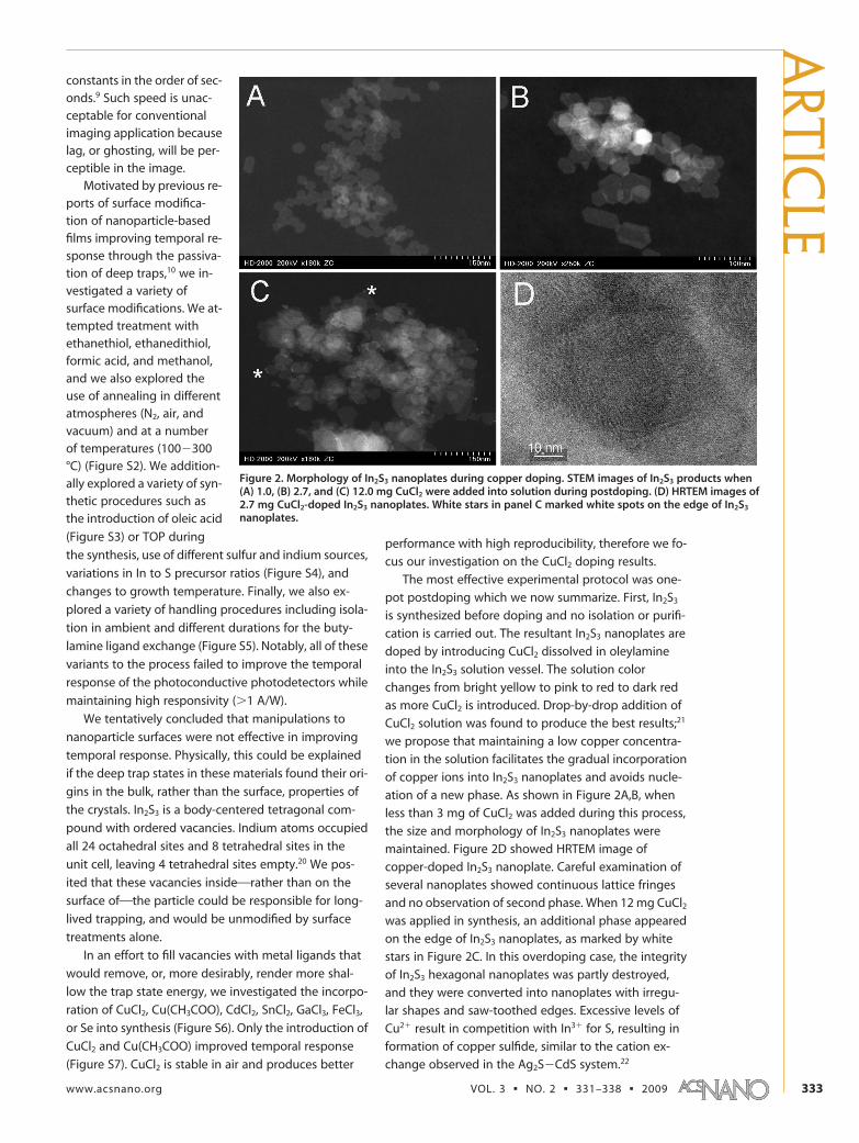
ation of a new phase. As shown in Figure 2A,B, when
less than 3 mg of CuCl2 was added during this process,
the size and morphology of In2S3 nanoplates were
maintained. Figure 2D showed HRTEM image of
copper-doped In2S3 nanoplate. Careful examination of
several nanoplates showed continuous lattice fringes
and no observation of second phase. When 12 mg CuCl2
was applied in synthesis, an additional phase appeared
on the edge of In2S3 nanoplates, as marked by white
stars in Figure 2C. In this overdoping case, the integrity
of In2S3 hexagonal nanoplates was partly destroyed,
and they were converted into nanoplates with irregu-
lar shapes and saw-toothed edges. Excessive levels of
Cu2� result in competition with In3� for S, resulting in
formation of copper sulfide, similar to the cation ex-
change observed in the Ag2S�CdS system.22
Figure 2. Morphology of In2S3 nanoplates during copper doping. STEM images of In2S3 products when(A) 1.0, (B) 2.7, and (C) 12.0 mg CuCl2 were added into solution during postdoping. (D) HRTEM images of2.7 mg CuCl2-doped In2S3 nanoplates. White stars in panel C marked white spots on the edge of In2S3
nanoplates.
ARTIC
LE
www.acsnano.org VOL. 3 ▪ NO. 2 ▪ 331–338 ▪ 2009 333

We carried out several experiments to ascertainwhether copper was truly being incorporated into In2S3.We sought first to confirm the presence of copper inour sample: after 3 days of butylamine ligand exchange,a process that should remove dopant not incorporatedinto the bulk but instead loosely bound to thesurface,23,24 we carried out ICP-AES measurements. Assummarized in Table 1, copper was detected in allsamples, including ligand-exchanged materials, intowhich CuCl2 had been added postsynthesis. In addi-tion, the composition calculated from ICP results agreedvery well with the value expected from added precur-sors, indicating nearly complete incorporation of cop-per into final products. We note sulfur content lies be-low its stoichiometric value in all samples, consistentwith the n-type nature of our materials further dis-cussed below.20,25
We then carried out powder XRD to investigatewhich crystalline phases were present in our syntheticproducts. As shown in Figure 3A, the XRD pattern ofcopper-doped sample showed characteristic peaks oftetragonal In2S3 (JCPDS 25-0390). We found evidence ofno phase other than �-In2S3. The strong broad peak at20° was also observed in InCl3 and oleylamine mixturewithout any treatment: we associate this peak with theIn3�-olelamine complex. Careful examination of theXRD patterns revealed no additional peaks associatedwith copper compounds such as CuO or Cu2S. This find-ing, that a single phase was present, agreed with STEMobservations discussed above that all nanoplates hadthe same contrast, as shown in Figure 2A and Figure 2B.
Taken together, these findingsOthat Cu is presentin the samples (ICP-AES), but does not form a secondphase (XRD and STEM)Osuggest that the Cu is indeedincorporated into the In2S3 lattice.
We sought to investigate the state in which Cudopants are in the lattice using electron paramagneticresonance (EPR) investigation. EPR characterization ofall our samples with 35 GHz Q-band at 77 K revealed nosignal, indicating that Cu2� is not present in oursamples.26 We conclude that copper exists as Cu� inour samples, a finding that is supported by XPS datashown in Figure 3B. The binding energy of Cu 2p3/2 is932.7 eV in our sample, characteristic of monovalentcopper.27 We believe Cu2� is reduced by oleylamine toCu� during the doping process. Oleyamine is widelyused to reduce sulfur or selenium in sulfide28 and se-lenide29 Cu2� to Cu� in chalcopyrite nanocrystal30 syn-
thesis, and Reihaneh Malakooti et al. proposed the
amine group could be oxidized into a nitroso group.31
However, the detailed reaction pathway is not clear yet.
TABLE 1. Composition of Copper-Doped In2S3 Expected from Added Precursor and Calculated from ICP Results
atomic percentage calculated from precursor atomic percentage determined from ICP
CuCl2 added in synthesis Cu In S Cu In S
0 mg 40.0 60.0 42.3 57.71.1 mg 0.4 39.9 59.8 0.4 41.8 57.82.7 mg 0.9 39.7 59.5 0.9 41.9 57.2
12.0 mg 3.5 38.6 57.9 3.8 39.2 57.0
Figure 3. (A) XRD patterns of undoped In2S3 nanoplates (red),copper-doped In2S3 nanoplates (black), and InCl3 and oley-lamine mixture (yellow); (B) XPS spectrum of copper incopper-doped In2S3; (C) absorption spectra of undoped anddoped In2S3 nanoplates in toluene solution.
ART
ICLE
VOL. 3 ▪ NO. 2 ▪ TANG ET AL. www.acsnano.org334
As further evidence of Cu� incorporation, we notethat the absorption spectrum of these materials showsa 50 nm shift in its onset following doping. Since quan-tum confinement is not at play in this material, this redshift is most likely a consequence of a bulk bandgapchange instead of a surface effect. Co2� doping in In2S3
has previously been reported to reduce the band gapof bulk In2S3 thin film from 1.98 to approximately 1.86eV.32 A similar shift appears to be at work in our Cu�-doped In2S3 nanoparticles.
In summary, these data indicate that our In2S3 nano-plates are doped with Cu� at concentrations rangingfrom 0.4% to 0.9% (for 1.1 mg and 2.7 mg CuCl2 in syn-thesis, respectively). Previous studies showed that for�2% Co2�- and �4% Cu�-doped In2S3 thin film,33,34 thedopants located in the Td symmetry site of the In2S3
host lattice, therefore we believe Cu� ions also fill intothe intrinsic tetragonal vacancies in our In2S3 nano-plates. Diffuse reflectance measurements of Cu��In2S3
materials could further clarify the details of Cu� incor-poration.34
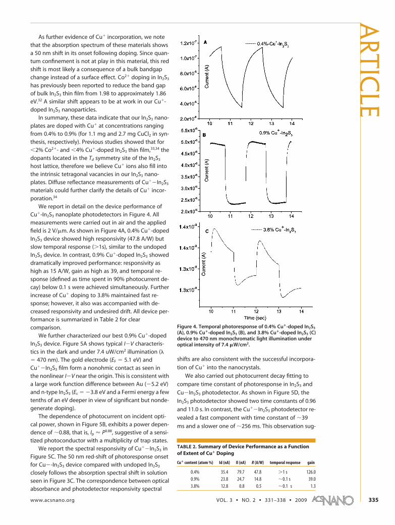
We report in detail on the device performance ofCu�-In2S3 nanoplate photodetectors in Figure 4. Allmeasurements were carried out in air and the appliedfield is 2 V/�m. As shown in Figure 4A, 0.4% Cu�-dopedIn2S3 device showed high responsivity (47.8 A/W) butslow temporal response (�1s), similar to the undopedIn2S3 device. In contrast, 0.9% Cu�-doped In2S3 showeddramatically improved performance: responsivity ashigh as 15 A/W, gain as high as 39, and temporal re-sponse (defined as time spent in 90% photocurrent de-cay) below 0.1 s were achieved simultaneously. Furtherincrease of Cu� doping to 3.8% maintained fast re-sponse; however, it also was accompanied with de-creased responsivity and undesired drift. All device per-formance is summarized in Table 2 for clearcomparison.
We further characterized our best 0.9% Cu�-dopedIn2S3 device. Figure 5A shows typical I�V characteris-tics in the dark and under 7.4 uW/cm2 illumination ( 470 nm). The gold electrode (EF 5.1 eV) andCu��In2S3 film form a nonohmic contact as seen inthe nonlinear I�V near the origin. This is consistent witha large work function difference between Au (�5.2 eV)and n-type In2S3 (Ec �3.8 eV and a Fermi energy a fewtenths of an eV deeper in view of significant but nonde-generate doping).
The dependence of photocurrent on incident opti-cal power, shown in Figure 5B, exhibits a power depen-dence of �0.88, that is, Ip � P0.88, suggestive of a sensi-tized photoconductor with a multiplicity of trap states.
We report the spectral responsivity of Cu��In2S3 inFigure 5C. The 50 nm red-shift of photoresponse onsetfor Cu�-In2S3 device compared with undoped In2S3
closely follows the absorption spectral shift in solutionseen in Figure 3C. The correspondence between opticalabsorbance and photodetector responsivity spectral
shifts are also consistent with the successful incorpora-
tion of Cu� into the nanocrystals.
We also carried out photocurrent decay fitting to
compare time constant of photoresponse in In2S3 and
Cu�In2S3 photodetector. As shown in Figure 5D, the
In2S3 photodetector showed two time constants of 0.96
and 11.0 s. In contrast, the Cu��In2S3 photodetector re-
vealed a fast component with time constant of �39
ms and a slower one of �256 ms. This observation sug-
Figure 4. Temporal photoresponse of 0.4% Cu�-doped In2S3
(A), 0.9% Cu�-doped In2S3 (B), and 3.8% Cu�-doped In2S3 (C)device to 470 nm monochromatic light illumination underoptical intensity of 7.4 �W/cm2.
TABLE 2. Summary of Device Performance as a Functionof Extent of Cu� Doping
Cu� content (atom %) Id (nA) Il (nA) R (A/W) temporal response gain
0.4% 35.4 79.7 47.8 �1 s 126.00.9% 23.8 24.7 14.8 �0.1 s 39.03.8% 12.8 0.8 0.5 �0.1 s 1.3
ARTIC
LE
www.acsnano.org VOL. 3 ▪ NO. 2 ▪ 331–338 ▪ 2009 335
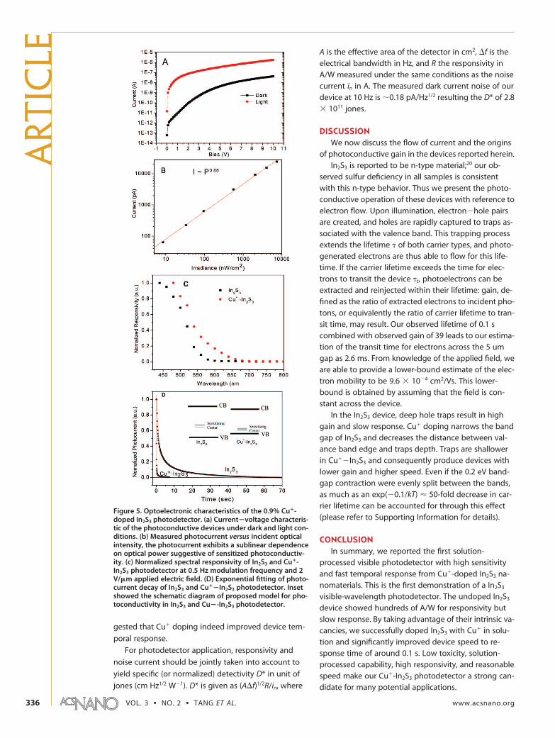
gested that Cu� doping indeed improved device tem-
poral response.
For photodetector application, responsivity and
noise current should be jointly taken into account to
yield specific (or normalized) detectivity D* in unit of
jones (cm Hz1/2 W�1). D* is given as (A�f)1/2R/in, where
A is the effective area of the detector in cm2, �f is theelectrical bandwidth in Hz, and R the responsivity inA/W measured under the same conditions as the noisecurrent in in A. The measured dark current noise of ourdevice at 10 Hz is �0.18 pA/Hz1/2 resulting the D* of 2.8 1011 jones.
DISCUSSIONWe now discuss the flow of current and the origins
of photoconductive gain in the devices reported herein.In2S3 is reported to be n-type material;20 our ob-
served sulfur deficiency in all samples is consistentwith this n-type behavior. Thus we present the photo-conductive operation of these devices with reference toelectron flow. Upon illumination, electron�hole pairsare created, and holes are rapidly captured to traps as-sociated with the valence band. This trapping processextends the lifetime � of both carrier types, and photo-generated electrons are thus able to flow for this life-time. If the carrier lifetime exceeds the time for elec-trons to transit the device �t, photoelectrons can beextracted and reinjected within their lifetime: gain, de-fined as the ratio of extracted electrons to incident pho-tons, or equivalently the ratio of carrier lifetime to tran-sit time, may result. Our observed lifetime of 0.1 scombined with observed gain of 39 leads to our estima-tion of the transit time for electrons across the 5 umgap as 2.6 ms. From knowledge of the applied field, weare able to provide a lower-bound estimate of the elec-tron mobility to be 9.6 10�4 cm2/Vs. This lower-bound is obtained by assuming that the field is con-stant across the device.
In the In2S3 device, deep hole traps result in highgain and slow response. Cu� doping narrows the bandgap of In2S3 and decreases the distance between val-ance band edge and traps depth. Traps are shallowerin Cu��In2S3 and consequently produce devices withlower gain and higher speed. Even if the 0.2 eV band-gap contraction were evenly split between the bands,as much as an exp(�0.1/kT) � 50-fold decrease in car-rier lifetime can be accounted for through this effect(please refer to Supporting Information for details).
CONCLUSIONIn summary, we reported the first solution-
processed visible photodetector with high sensitivityand fast temporal response from Cu�-doped In2S3 na-nomaterials. This is the first demonstration of a In2S3
visible-wavelength photodetector. The undoped In2S3
device showed hundreds of A/W for responsivity butslow response. By taking advantage of their intrinsic va-cancies, we successfully doped In2S3 with Cu� in solu-tion and significantly improved device speed to re-sponse time of around 0.1 s. Low toxicity, solution-processed capability, high responsivity, and reasonablespeed make our Cu�-In2S3 photodetector a strong can-didate for many potential applications.
Figure 5. Optoelectronic characteristics of the 0.9% Cu�-doped In2S3 photodetector. (a) Current�voltage characteris-tic of the photoconductive devices under dark and light con-ditions. (b) Measured photocurrent versus incident opticalintensity, the photocurrent exhibits a sublinear dependenceon optical power suggestive of sensitized photoconductiv-ity. (c) Normalized spectral responsivity of In2S3 and Cu�-In2S3 photodetector at 0.5 Hz modulation frequency and 2V/�m applied electric field. (D) Exponential fitting of photo-current decay of In2S3 and Cu��In2S3 photodetector. Insetshowed the schematic diagram of proposed model for pho-toconductivity in In2S3 and Cu�-In2S3 photodetector.
ART
ICLE
VOL. 3 ▪ NO. 2 ▪ TANG ET AL. www.acsnano.org336

METHODSIn2S3 and Cu��In2S3 Nanoplates Synthesis. All chemicals used were
purchased from Sigma-Aldrich. Oleylamine was pumped with aSchlenk line at 80 °C for 1 day, butylamine was distilled beforeuse. All other materials were used without further purification.Synthesis was conducted under inert atmosphere using aSchlenk line and isolated in a glovebox. Synthesis of In2S3 nano-plates is described elsewhere.19 For Cu��In2S3 nanoplates, wefirst mixed 1 mmol InCl3, 1.5 mmol sulfur powder, and 10 mL ofoleyalmine and pumped at 120 °C for 1 h to produce a clearbrown solution. Afterward N2 was introduced into the reactingvessel and heated the solution to 215 °C and incubated for 1 hto produce In2S3 nanoplates. Then a given amount of CuCl2 dis-solved in 5 mL oleylamine was injected into the flask drop bydrop with syringe. This injection process lasted for 40 min andthe solution color changed from yellow to red. After injection,the solution was maintained at 215 °C for another 40 min. Aftercooling naturally to room temperature, the flask was sealed andtransferred into glovebox for isolation. The raw solution waswashed first by toluene and precipitated by methanol, and re-peated this process twice. Finally the precipitates were collectedand dried for ligand exchange.
Ligand Exchange, Device Fabrication, and Treatment. Butyamineligand exchange and device produce were done at inert atmo-sphere in a glovebox. Typically we dispersed all sediments col-lected during isolation into 10 mL of distilled butylamine andstored them undisturbed for 2 days. Afterward In2S3 nanomate-rials were precipitated by methanol and redispersed in 5 mL oftoluene to produce concentrated solution. Photodetector wasfabricated by dropping 10 �L of such solution onto precleanedinterdigitated gold electrodes and dried naturally. When the de-vice was ready, we transferred it into vacuum oven (preheatedto 200 °C) and annealed under vacuum for 10 min. Device wasmeasured in air.
Characterization. Visible�near-NIR absorption spectra of thenanomaterials in toluene were recorded at room temperatureusing a Cary 500 UV�vis�near-IR spectrophotometer. FTIR spec-tra were obtained using a Bruker Tensor 27 infrared spectrom-eter. Samples were prepared by drop-casting the same volumeof In2S3 toluene solution before and after butyalmine ligand ex-change onto KBr substrates, after which the samples were driedin air and produced films with approximately identical thickness.XRD was recorded with a Siemens diffractemeter with Cu K� ra-diation ( 1.54178 Å). ICP measurements were performed us-ing a Perkin-Elmer model Optima 3000DV ICP AEOS. XPS was re-corded at a PHI 5500 (XPS) spectrometer. Samples were preparedby drop-casting nanoparticle from toluene onto gold film sput-tered on top of undoped silicon wafer. EPR was done on VarianE-9 EPR multifrequency spectrometer using 35 GHz Q-band at 77K.The size and morphology of as-synthesized samples were char-acterized on Hitachi HD-2000 scanning transmission electron mi-croscopy. We prepared the sample by putting one drop of In2S3
or Cu�-In2S3 toluene solution onto 300 mesh carbon/Formvarcopper grid. HRTEM images were taken on Titan TM 80-300 us-ing holey carbon film on Ni grid as substrate. SEM characteriza-tion was done on Hitachi S-5200 scanning electron microscopy.SEM sample was prepared by drop-casting In2S3 solution ontoclean ITO substrate. Film thickness was measured with a VeecoDektak3 surface profiler.
All current�voltage measurements were taken with an Agi-lent 4155C semiconductor parameter analyzer. The device wastop-illuminated using an overhead blue LED operating at 470nm. Optical intensity was measured with a Melles-Griot broad-band power meter. The active device area was fixed as 0.015mm2 throughout the whole experiments. Dark current noise inthe photodetectors was measured using a Stanford ResearchSR830 lock-in amplifier. The devices were biased using alkalinebatteries at 10 V and testing was carried out in an electricallyshielded and optically sealed probe station on a floating tableto minimize vibrational noise. Knowing device area, responsiv-ity, and the noise current normalized to the measurement band-width, we were able to obtain the D* normalized detectivityvalue of our device as reported in the text.
Acknowledgment. We acknowledge Dr. Christopher C. Felixand Dr. William Antholine at the National Biomedical EPR Cen-ter and Medical College of Wisconsin for their help with EPR mea-surements. We thank Dr. L. Levina, G. Koleilat, E. Klem, V. Sukho-vatkin, M. Yang, and A. Barkhouse for their help during thecourse of this study. J. Tang would like to thank Dr. Dan Mathers,Dr. Neil Coombs, Dr. S. Petrov, Dr. D. Grozea, Dr. G. de Silveira,Dr. C. Andrei, and L. Gunawan for their kind help in measure-ments and Dr. H. Z. Zhong and K. Tsai for productive discussion.
Supporting Information Available: SEM characterization ofIn2S3 film, details of many “failed” examples of trap manipula-tion as well as theoretical calculation of change of trap activa-tion energy after Cu�-doping. This material is available free ofcharge via the Internet at http://pubs.acs.org.
REFERENCES AND NOTES1. Konstantatos, G.; Howard, I.; Fischer, A.; Hoogland, S.;
Clifford, J.; Klem, E.; Levina, L.; Sargent, E. H. UltrasensitiveSolution-Cast Quantum Dot Photodetectors. Nature 2006,442, 180–183.
2. Konstantatos, G.; Clifford, J.; Levina, L.; Sargent, E. H.Sensitive Solution-Processed Visble WavelengthPhotodetectors. Nat. Photon. 2007, 1, 531–534.
3. Qi, D. F.; Fischbein, M.; Drndic, M.; Selmic, S. EfficientPolymer-Nanocrystal Quantum-Dot Photodetectors. Appl.Phys. Lett. 2005, 86, 093103-1–093103-3.
4. Oertel, D. C.; Bawendi, M. G.; Arango, A. C.; Bulovic, V.Photodetectors Based on Treated CdSe Quantum-DotFilms. Appl. Phys. Lett. 2005, 87, 213505-1–213505-3.
5. Dindar, A.; Therrien, J. A Resonant Tunneling CdSeQuantum Dot Photodetector for Spectral Resolution in theVisible Region. Proc. SPIE 2007, 6479, 64790U1–64790U8.
6. Amos, F. F.; Morin, S. A.; Streifer, J. A.; Hamers, R. J.; Jin, S.Photodetector Arrays Directly Assembled onto PolymerSubstrates from Aqueous Solution. J. Am. Chem. Soc. 2007,129, 14296–14302.
7. Yotter, R. A.; Wilson, D. M. A Review of Photodetectors forSensing Light-Emitting Reporters in Biological Systems.IEEE Sens. J. 2003, 3, 288–303.
8. Fossum, E. R. Digital Camera System on a Chip. IEEE Micro1998, 18, 8–15.
9. Jin, Y.; Wang, J.; Sun, B.; Blakesley, J. C.; Greenham, N. C.Solution-Processed Ultraviolet Photodetectors Based onColloidal ZnO Nanoparticles. Nano. Lett. 2008, 8,1649–1653.
10. Konstantatos, G.; Levina, L.; Fischer, A.; Sargent, E. H.Engineering the Temporal Response of PhotoconductivePhotodetectors via Selective Introduction of Surface TrapStates. Nano Lett. 2008, 8, 1446–1450.
11. Urban, J. J.; Talapin, D. V.; Shevchenko, E. V.; Kagan, C. R.;Murray, C. B. Synergism in Binary Nanocrystal SuperlatticesLeads to Enhanced p-type Conductivity in Self-Assembled PbTe/Ag2Te Thin Films. Nat. Mater. 2007, 6,115–121.
12. Talapin, D. V.; Murray, C. B. PbSe Nanocrystal Solids for n-and p-Channel Thin Film Field-Effect Transistors. Science2005, 310, 86–89.
13. Coe, S.; Woo, W. K.; Bawendi, M.; Bulovic, V.Electroluminescence from Single Monolayers ofNanocrystals in Molecular Organic Devices. Nature 2002,420, 800–803.
14. Gur, I.; Fromer, N. A.; Geier, M. L.; Alivisatos, A. P. Air-StableAll-Inorganic Nanocrystal Solar Cells Precessed fromSolution. Science 2005, 21, 462–465.
15. Luther, J. M.; Law, M.; Beard, M. C.; Song, Q.; Reese, M. O.;Ellingson, R. J.; Nozik, A. J. Schottky Solar Cells Based onColloidal Nanocrystal Films. Nano Lett. 2008, 8, 3488–3492.
16. Jayakrishnan, R.; John, T. T.; Kartha, C. S.; Vijayakumar, K. P.;Jain, D.; Chandra, L. S. S.; Ganesan, V. Do the GrainBoundaries of �-In2S3 Thin Films Have a Role in Sub-
ARTIC
LE
www.acsnano.org VOL. 3 ▪ NO. 2 ▪ 331–338 ▪ 2009 337

Band-Gap Photosensitivity to 632.8 nm. J. Appl. Phys. 2008,103, 053106-1–053106-6.
17. Norris, D. J.; Efros, A. L.; Erwin, S. C. Doped Nanocrystals.Science 2008, 319, 1776–1779.
18. Dalpian, G. M.; Chelikowsky, J. R. Self-Purification inSemiconductor Nanocrystals. Phys. Rev. Lett. 2006, 96,226802-1–226802-4.
19. Park, K. H.; Jang, K.; Son, S. U. Synthesis, Optical Properties,and Self-Assembly of Ultrathin Hexagonal In2S3
Nanoplates. Angew. Chem., Int. Ed. 2006, 45, 4608–4612.20. Rehwald, W.; Harbeke, G. On the Conduction Mechanism
in Single Crystal �-Indium Sulfide In2S3. J. Phys. Chem. Solid1965, 26, 1309–1318.
21. Mixed InCl3, CuCl2, and sulfur powder at the beginningand then cooked also produced copper-doped In2S3 butwith large size and morphology distribution. Directinjection of CuCl2 solution into the reaction vesselrendered a sudden burst of copper concentration insolution, leading to porous copper-doped In2S3
nanoplates.22. Son, D. H.; Hughes, S. M.; Yin, Y. D.; Alivisatos, A. P. Cation
Exchange Reactions in Ionic Nanocrystals. Science 2004,306, 1009–1012.
23. Mikulec, F. W.; Kuno, M.; Bennati, M.; Hall, D. A.; Griffin,R. G.; Bawendi, M. G. Organometallic Synthesis andSpectroscopic Characterization of Manganese-DopedCdSe Nanocrystals. J. Am. Chem. Soc. 2000, 122,2532–2540.
24. Nag, A.; Chakraborty, S.; Sarma, D. D. To Dope Mn2� in aSemiconducting Nanocrystal. J. Am. Chem. Soc. 2008, 130,10605–10611.
25. John, T. T.; Bini, S.; Kashiwaba, Y.; Abe, T.; Yasuhiro, Y.;Kartha, C. S.; Vijayakumar, K. P. Characterization of SprayPyrolysed Indium Sulfide Thin Films. Semicond. Sci.Technol. 2003, 18, 491–500.
26. Massa, M. B.; Dalosto, S. D.; Ferreyra, M. G.; Labadie, G.;Calvo, R. Vibronic Behavior and Single-Crystal EPR Spectraof Cu(II) in Copper-Doped Diaqua(L-aspartato)zinc(II)Hydrate. J. Phys. Chem. A 1999, 103, 2606–2617.
27. NIST X-ray Photoelectron Spectroscopy Database, http://srdata.nist.gov/xps/ (accessed October, 2008).
28. Joo, J.; Na, H. B.; Yu, T.; Yu, J. H.; Kim, Y. W.; Wu, F. X.;Zhang, J. Z.; Hyeon, T. Generalized and Facile Synthesis ofSemiconducting Metal Sulfide Nanocrystals. J. Am. Chem.Soc. 2003, 125, 11100–11105.
29. Park, K. H.; Jang, K. J.; Kim, S. Y.; Kim, H. J.; Son, S. K. Phase-Controlled One-Dimensional Shape Evolution of InSeNanocrystals. J. Am. Chem. Soc. 2006, 128, 14780–14781.
30. Tang, J.; Hinds, S.; Kelley, S. O.; Sargent, E. H. Synthesis ofColloidal CuGaSe2, CuInSe2, and Cu(InGa)Se2
Nanoparticles. Chem. Mater. 2008, 20, 6906–6910.31. Malakooti, R.; Cademartiri, L.; Akcakir, Y.; Petrov, S.;
Migliori, A.; Ozin, G. A. Shape-Controlled Bi2S3 Nanocrystalsand Their Plasma Polymerization into Flexible Films. Adv.Mater. 2006, 18, 2189–2194.
32. Kim, C. D.; Lim, H.; Park, H. L.; Park, H. Y.; Kim, J. E.; Kim,H. G.; Kim, Y. G.; Kim, W. T. Optical Absorption of Co2� ionsin In2S3 Thin Films. Thin Solid Films 1993, 224, 69–73.
33. Kim, W. T.; Lee, W. S.; Chung, C. S.; Kim, C. D. OpticalProperties of In2S3:Co2� Single Crystals. J. Appl. Phys. 1988,63, 5472–5475.
34. Py, F.; Womes, M.; Durand, J. M.; Olivier-Fourcade, J.;Jumas, J. C. Copper in In2S3: A Study by X-ray Diffraction,Diffuse Reflectance and X-ray Absorption. J. Alloys Compd.1992, 178, 297–304.
ART
ICLE
VOL. 3 ▪ NO. 2 ▪ TANG ET AL. www.acsnano.org338