Halogenated Graphenes: Rapidly Growing Family of Graphene Derivatives
31
KARLICKÝ ET AL . VOL. 7 ’ NO. 8 ’ 6434–6464 ’ 2013 www.acsnano.org 6434 June 28, 2013 C 2013 American Chemical Society Halogenated Graphenes: Rapidly Growing Family of Graphene Derivatives Franti sek Karlick y, Kasibhatta Kumara Ramanatha Datta, Michal Otyepka, * and Radek Zbo ril * Regional Centre of Advanced Technologies and Materials, Department of Physical Chemistry, Faculty of Science, Palack y University, 17. listopadu 1192/12, 771 46 Olomouc, Czech Republic G raphene, comprising a single layer of sp 2 -bonded carbon atoms ar- ranged in a honeycomb lattice, was the first two-dimensional atomic crys- tal to be identified. Since its initial isola- tion in 2004, many studies have shown that this one-atom-thick material of carbon uniquely combines superior mechanical strength, remarkably high electronic and thermal conductivities, high surface area, and impermeability to gases, in addition to many other desirable properties, all of which make it highly attractive for numerous applications. 1 Many of the unique physical properties of graphene stem from its unusual electronic structure near the Fermi level. 2 The ability to tailor its properties, especially the opening of a band gap, is critical for its potential use in several (opto)electronic applications. 3 In the past few years, covalently modi- fied graphene derivatives prepared by at- tachment of hydrogen, halogens, or other atoms have attracted considerable interest for their potential applications (e.g., in elec- tronic devices). 46 The relative simplicity of atomic adsorbates allows them to be also well described by theoretical calculations. 7 The idea to fully hydrogenate graphene was put forward in 2003 ahead of graphene's isolation, and several possible geometrical structures were considered, 8 even though at that stage it was clearly a hypothetic material. In 2007, fully hydrogenated gra- phene was named graphane by Sofo et al., 9 who also discussed its electronic properties and its fluorinated counterpart. Two years later, graphane was synthesized as a stable material under ambient conditions by expo- sure of graphene to cold hydrogen plasma. 10,11 The fully fluorinated graphene counterpart, fluorographene (graphene fluoride, C 1 F 1 ), was prepared experimentally in 2010 (refs 1214) by chemical and mechanical exfoliation of graphite fluoride, that is, by approaches that had been successfully ap- plied to prepare graphene from graphite. Graphite fluoride is a well-known graphite derivative (fluorine-intercalated compound) 15 with covalent CF bonds. Although bulk graphite fluoride has been used as a lubricant * Adress correspondence to [email protected], [email protected]. Received for review May 13, 2013 and accepted June 28, 2013. Published online 10.1021/nn4024027 ABSTRACT Graphene derivatives containing covalently bound halogens (graphene halides) represent promising two-dimensional systems having inter- esting physical and chemical properties. The attachment of halogen atoms to sp 2 carbons changes the hybridization state to sp 3 , which has a principal impact on electronic properties and local structure of the material. The fully fluorinated graphene derivative, fluorographene (graphene fluoride, C 1 F 1 ), is the thinnest insulator and the only stable stoichiometric graphene halide (C 1 X 1 ). In this review, we discuss structural properties, syntheses, chemistry, stabilities, and electronic properties of fluorographene and other partially fluorinated, chlorinated, and brominated graphenes. Remarkable optical, mechanical, vibrational, thermodynamic, and conductivity properties of graphene halides are also explored as well as the properties of rare structures including multilayered fluorinated graphenes, iodine-doped graphene, and mixed graphene halides. Finally, patterned halogenation is presented as an interesting approach for generating materials with applications in the field of graphene-based electronic devices. KEYWORDS: graphane . graphene semiconductor . fluorination . doping . magnetic graphene . band gap opening . chlorographene . chlorination . graphene oxide . graphene dot REVIEW
Transcript of Halogenated Graphenes: Rapidly Growing Family of Graphene Derivatives

KARLICKÝ ET AL . VOL. 7 ’ NO. 8 ’ 6434–6464 ’ 2013
www.acsnano.org
6434
June 28, 2013
C 2013 American Chemical Society
Halogenated Graphenes: RapidlyGrowing Family of GrapheneDerivativesFranti�sek Karlick�y, Kasibhatta Kumara Ramanatha Datta, Michal Otyepka,* and Radek Zbo�ril*
Regional Centre of Advanced Technologies and Materials, Department of Physical Chemistry, Faculty of Science, Palack�y University, 17. listopadu 1192/12,771 46 Olomouc, Czech Republic
Graphene, comprising a single layerof sp2-bonded carbon atoms ar-ranged in a honeycomb lattice,
was the first two-dimensional atomic crys-tal to be identified. Since its initial isola-tion in 2004, many studies have shownthat this one-atom-thickmaterial of carbonuniquely combines superior mechanicalstrength, remarkably high electronic andthermal conductivities, high surface area, andimpermeability to gases, in addition to manyother desirableproperties, all ofwhichmake ithighly attractive for numerous applications.1
Many of the unique physical properties ofgraphene stem from its unusual electronicstructure near the Fermi level.2 The abilityto tailor its properties, especially the openingof a band gap, is critical for its potential use inseveral (opto)electronic applications.3
In the past few years, covalently modi-fied graphene derivatives prepared by at-tachment of hydrogen, halogens, or otheratoms have attracted considerable interestfor their potential applications (e.g., in elec-tronic devices).4�6 The relative simplicity of
atomic adsorbates allows them to be alsowell described by theoretical calculations.7
The idea to fully hydrogenate graphenewasput forward in 2003 ahead of graphene'sisolation, and several possible geometricalstructures were considered,8 even thoughat that stage it was clearly a hypotheticmaterial. In 2007, fully hydrogenated gra-phene was named graphane by Sofo et al.,9
who also discussed its electronic propertiesand its fluorinated counterpart. Two yearslater, graphane was synthesized as a stablematerial under ambient conditions by expo-sureofgraphene tocoldhydrogenplasma.10,11
The fullyfluorinatedgraphene counterpart,fluorographene (graphene fluoride, C1F1),was prepared experimentally in 2010(refs 12�14) by chemical and mechanicalexfoliation of graphite fluoride, that is, byapproaches that had been successfully ap-plied to prepare graphene from graphite.Graphite fluoride is a well-known graphitederivative (fluorine-intercalatedcompound)15
with covalent C�F bonds. Although bulkgraphite fluoride has been used as a lubricant
* Adress correspondence [email protected],[email protected].
Received for review May 13, 2013and accepted June 28, 2013.
Published online10.1021/nn4024027
ABSTRACT Graphene derivatives containing covalently bound halogens
(graphene halides) represent promising two-dimensional systems having inter-
esting physical and chemical properties. The attachment of halogen atoms to sp2
carbons changes the hybridization state to sp3, which has a principal impact on
electronic properties and local structure of the material. The fully fluorinated
graphene derivative, fluorographene (graphene fluoride, C1F1), is the thinnest
insulator and the only stable stoichiometric graphene halide (C1X1). In this
review, we discuss structural properties, syntheses, chemistry, stabilities, and
electronic properties of fluorographene and other partially fluorinated, chlorinated, and brominated graphenes. Remarkable optical, mechanical,
vibrational, thermodynamic, and conductivity properties of graphene halides are also explored as well as the properties of rare structures including
multilayered fluorinated graphenes, iodine-doped graphene, and mixed graphene halides. Finally, patterned halogenation is presented as an interesting
approach for generating materials with applications in the field of graphene-based electronic devices.
KEYWORDS: graphane . graphene semiconductor . fluorination . doping .magnetic graphene . band gap opening . chlorographene .chlorination . graphene oxide . graphene dot
REVIEW
KARLICKÝ ET AL . VOL. 7 ’ NO. 8 ’ 6434–6464 ’ 2013
www.acsnano.org
6435
for nearly 100 years and has also been exploited as anexcellent electrode material in primary lithium batteries,graphene fluoride was not experimentally realizeduntil 2010. Alternative ways of preparing fluorinatedgraphene12,16 or graphite17,18 by cold plasma weredeveloped simultaneously. However, this approachoften generates nonstoichiometricfluorinatedgraphenes(C1Fa, a < 1). The attachment of fluorine atoms to sp2
carbons changes the hybridization state to sp3 (Figure 1aand Figure 1b), which significantly affects the electronicproperties and local structure of thematerial but preservesthe 2D hexagonal symmetry. Such structural changesinduce opening of the zero band gap of graphene atthe K point and lead to loss of the π-conjugated electroncloud above and below the graphene plane. The chargecarrier mobility has been shown to be 3 orders of magni-tude smaller for fluorographene in comparison to gra-phene, and fluorographene behaves like an insulator witha minimal direct band gap at the Γ point (Figure 1c,d).To date, dozens of experimental and theoretical
papers on halogenated graphenes have been pub-lished. Besides the stoichiometric fluorographene, nu-merous partially fluorinated graphenes have also beensynthesized,19�24 where the degree of fluorinationenables control over the electronic properties, whichmight be utilized in band gap engineering of 2Dcarbon-based materials. Contrary to fluorographene,the fully chlorinated counterpart has not been yet pre-pared, while partially chlorinated25�28 or brominated27,28
graphene derivatives have been reported very recently.Halogenated graphenes exhibit a plethora of remarkableand interesting electronic, optical, thermal, electrocataly-tic, magnetic, mechanical, biological, and chemical prop-erties in comparison with their graphene counterparts.Here, we classify the graphene halides and review
preparation approaches, properties, and applications ofhalogenated graphenes. The review provides a complexoverview as it considers both experimental and theore-tical aspects of graphene halogenation. First, the synthe-sis of graphene halides is discussed. Next, properties offluorographene and partially fluorinated graphenes aresummarized including insightful theoretical studies.These sections focus on structural and vibrational proper-ties, which can be used as fingerprints of the consideredmaterials, as well as electronic, optical, and mechanicalproperties of graphenehalides,whichare important froman application perspective. Next, we summarize recentprogressonchlorinatedandbrominatedgraphenes fromboth theoretical and experimental standpoints. Finally,we discuss patterned structures on graphene.
Synthesis of Graphene Halides. Synthesis of Fluorogra-phene and Fluorinated Graphenes. There are twomain methods to prepare fluorographenes.12,13,16
One approach involves transformation of graphenesto fluorographenes by fluorination using an appro-priate fluorinating agent (see below).12,16 The otherprocedure utilizes chemical or mechanical exfoliation
of pristine graphite fluoride, i.e., the same techniquesthat have been successfully applied for the preparationof graphene from graphite.29,30
Fluorographene can be prepared by fluorinatinggraphene using XeF2 at various temperatures under aninert atmosphere (Figure 2a)12,31 or at room temperature(30 �C).16 The room temperature preparation of fluoro-graphene involves fluorinating graphene supported ona silicon-on-insulator substrate using XeF2 gas, whichselectively etches the Si underlayer and fluorinates bothsides of the graphene to form fully fluorinated graphenewith a dominant stoichiometry of C1.0F1.0.
16 In addition,fluorination of highly oriented pyrolitic graphite (HOPG)by fluorine gas under high temperature (600 �C) andsubsequent chemical exfoliationhasbeen shown to yielda nonstoichiometric fluorographene (C1F0.7) of low qual-ity owing to numerous structural defects caused bythe harsh preparation conditions.17 It should be noted,that fluorination of graphene grown by chemical vapordeposition (CVD) on copper has been reported to yield asingle side partially fluorinated graphene with dominantstoichiometry of CF0.25.
16
VOCABULARY:: graphene derivatives � a class of
materials having two-dimensional scaffold, which are de-
rived from graphene by covalent attachment of atoms,
functional groups or molecular moieties. Graphane, gra-
phene oxide, and fluorographene represent the typical
examples of graphene derivatives;fluorographene �stoichiometric C1F1 derivative of graphene with the fluor-
ine atom attached to each carbon atom thus having sp3
hybridization. Fluorographene can be prepared by gra-
phene fluorination or exfoliation of graphite fluoride.
Fluorographene represents still the only stoichiometric
graphene halide stable at ambient conditions;haloge-
nated graphenes � graphene derivatives, in which some
carbon atoms are covalently linked with halogen atoms.
The carbon atoms linked with halogens have sp3 hybridi-
zation and others have sp2 hybridization. The physico-
chemical properties of graphene halides are strongly
dependent on a degree of halogenation;patterned halo-
genation � the outcome of placing masks or metal grids
over graphene during halogenation process is known as
patterned halogenation. Uncovered regions of the gra-
phene become halogenated and the masked regions
remain intact and can be used as conductive pathways
for device fabrication or construction of graphene super-
structures;bandgapengineering�graphene lacks aband
gap because its valence and conduction bands touch each
other, and it is labeled as a semimetal. The lackingbandgap
limits usage of graphene in contemporary electronic de-
vices. The band structure of graphene can be modified to
open the band gap by many strategies, e.g., halogenation,
oxidation, hydrogenation or noncovalent attachment of
variousmolecules and species. A complexwayhow to open
and tune the band gap in graphene and its derivatives is
termed as band gap engineering;
REVIEW

KARLICKÝ ET AL . VOL. 7 ’ NO. 8 ’ 6434–6464 ’ 2013
www.acsnano.org
6436
Stoichiometric fluorographene can also be preparedby a top-down approach employing mechanical12,14 orchemical13,23,32 exfoliation of graphite fluoride. Gra-phene fluoride in the form of colloidal suspensionscan be obtained by chemically etching bulk graphitefluoride via sonication in the presence of sulfolane,13
dimethylformamide (DMF),32 orN-methyl-2-pyrrolidone(NMP)23 (Figure 2b). In this process, the solvent mol-ecules intercalate within the interlayers, weakening thevan der Waal's interactions between neighboring layersand facilitating the exfoliation of graphite fluoride intocolloidal fluorographenes. In the case of mechanicalexfoliation, the as prepared fluorographene mono-layers are of high quality and are suitable for physicalexperiments. However, such an approach is difficultto scale-up for potential applications. On the otherhand, chemical exfoliation enables preparation of largeamounts of graphene fluoride. However, polydispersivesystems are formed containing one- and few-layerfluorographenes. Nonetheless, the solution processabil-ity of fluorographene colloids could be advantageous inthe field of coatings, polymer nanocomposites, etc.
Fluorinated graphene with different fluorineloadings can be achieved by fluorinating grapheneor chemically etching nonstoichiometric graphene fluo-ride. Briefly, fluorination of graphene or reduced gra-phene oxide sheets (mono- and multilayered) is usuallycarried out in plasmas containing CF4 (refs 33, 34) andSF6,
35 XeF2,36,37
fluoropolymers20 or Ar/F2 (ref 38) asfluorinating agents. The fluorine content of the result-ing fluorinated graphenes can be varied by changingthe plasma treatment time as well as the fluorinatingagent.33,36,39
Recently, Ruoff and co-workers20 have developeda versatile and environmentally friendly approach forselective or patterned fluorination of graphene (on aSiO2/Si substrate) using the fluoropolymer CYTOPcombined with laser irradiation. In this method, directcontact between CYTOP and the graphene surface isachieved by transferring graphene films on Cu foilonto a SiO2/Si substrate coated with CYTOP. After laserirradiation, photon-induced decomposition of CYTOPgeneratesmany active intermediates, such as CFx and Fradicals, which react with sp2 hybridized grapheneforming C�F sp3 bonds (Figure 2c). This process yieldssingle side fluorination (25% coverage) as the activefluorine species cannot penetrate through the SiO2/Sisubstrate.
Similar to the isolation of fluorographenes frombulk graphite fluoride via chemical etching, fluorinatedgraphenes can be exfoliated fromgraphite fluoridewithdifferent fluorine contents in various solvents with/without surfactants via sonication19,24,40 or mechanicalexfoliation.41 Fluorinated graphenes with compositionsCF0.25 and CF0.5 have been obtained by exfoliatinggraphite fluoride with fluorinated ionic liquids, asdescribed by Zheng et al.19 Very recently, multilayersemi-ionically fluorinated graphene was prepared usinga one-pot synthesis employing liquid ClF3 and graphite(5 h). The obtained sample was subsequently mechani-cally exfoliated to single and bilayer films.42,43
Fluorine-doped multilayered graphene (10 wt %,i.e., 6.6 atom %) has been synthesized using an arcdischarge process in which a hollow graphite rod isfilled with powdery graphite fluoride.22 The fluorinecontent of the graphene matrix can also be tuned
Figure 1. (a) Hexagonal structure of sp2 carbons in graphene. (b) Transformation to sp3 carbons by fluorination in the chairconformation of fluorographene. Electronic band structures of (c) graphene and (d) fluorographene. The original graphenezero band gap at the K point is opened to a band gap with minimal value of several eV at the Γ point (red circles).
REVIEW

KARLICKÝ ET AL . VOL. 7 ’ NO. 8 ’ 6434–6464 ’ 2013
www.acsnano.org
6437
by the chemical reaction of graphene oxide withhydrofluoric acid.21 Fluorination of graphene oxidecan be done by exposing graphene oxide to anhydrousHF vapors at various temperatures44 or photochemi-cally at room temperature using HF solution.45
Synthesis of Other Halogenated Graphenes. Re-cently, a nondestructive and patternable photochemi-cal chlorination treatment of single- and few-layergraphene has been used to produce a material withstoichiometry CCl0.08.
25 The chemical patterning wasachieved using a chlorine-resistant Al/Ti mask to pro-tect selected regions of graphene from photochlorina-tion. In this approach, chlorine radicals covalentlyattach to the basal carbon atoms of the graphene(C�Cl), transforming from a sp2 to sp3 configurationand creating high structural disorder. The chlorineplasma technique allows controlled p-type doping
of graphene sheets and graphene nanoribbons.26
The chlorination of graphene occurs in two stages: inthe first stage, chlorination occurs rather nondestruc-tively and reversibly, whereas in the second stageat longer exposure times (>2 min), larger-area defectsbegin to form irreversibly. Graphene nanoribbons(GNR) supported on SiO2/Si and exposed to Cl plasma(1 min) showed a 1.3�2.2 fold increase in conductance(in ambient air). Similarly, after Cl plasma treatment for10 s, graphene sheets showed a slight increase (withrespect to GNR) in conductance, whereas longer exposureresulted in reduced conductivity. Compared to fluorina-tion andhydrogenation, the chlorineplasma reactionwithgraphene exhibits the slowest kinetics, showing only aslow increase in disorder with reaction time.
Recently, Rao and co-workers28 prepared few-layerchlorinated andbrominated graphenes up to 30 atom%
Figure 2. (a) Various steps involved in the fluorination of graphene (PMMA � poly(methyl methacrylate)). Reprinted withpermission from ref 12. Copyright 2010Wiley. (b) Schematic of the NMP intercalation and exfoliation fabrication processes used toprepare CF dispersions. Reprintedwith permission from ref 23. Copyright 2012 Royal Society of Chemistry. (c) Scheme showing themechanism of fluorination using CYTOP and laser irradiation. Reprinted from ref 20. Copyright 2012 American Chemical Society.
REVIEW

KARLICKÝ ET AL . VOL. 7 ’ NO. 8 ’ 6434–6464 ’ 2013
www.acsnano.org
6438
(CCl0.43) and 5 atom % (CBr0.05), respectively, usingultraviolet (UV) irradiation in liquid chlorine or liquidbromine media. A microwave-spark (MiW-S) assistedreaction has also been developed that allows thedirect production of Cl and Br-functionalizedmonolayergraphene sheets from graphite.27 During microwaveirradiation, graphite was shown to expand to 200 timesits original volume accompanied by luminous sparksand moderate ionization of the halogens (Xþ). Theionized halogen atoms readily attacked the π-ring ofgraphene, resulting in halogenation, probably via anelectrophilic substitution mechanism. The amount of Clatoms on the graphene sheets was up to 21 atom %(CCl0.27), whereas Brwas 4 atom% (CBr0.04), asmeasuredby XPS analysis.27 Chlorination was shown to be moreeffective than bromination as liquid Cl2 is more reactivethan Br2.
27,28 Thermal annealing or laser irradiation ofthe prepared chlorinated graphene samples completelyremoved the chlorine to obtain pristine graphene.27,28
Interestingly, the halogen atoms in the resulting CXcould be substituted/modified by other organic func-tional groups under conventional organic reaction con-ditions, which opens up other possibilities for preparinggraphene derivatives.27
Iodine-doped graphenes with an iodine loadingof 3 atom % have been prepared by direct heating ofcamphor and I2.
46 In addition, exfoliation of grapheneoxide and I2 under ultrasonic treatment followedby thermal annealing at various temperatures (500�1100 �C) has been shown to generate iodine-dopedgraphenes (1.2�0.8 wt %, i.e., ∼0.1 atom %).47 Veryrecently, halogenated graphenes have been preparedby the thermal exfoliation of graphite oxide underdifferent gaseous halogen atmospheres (chlorine, bro-mine, or iodine),48 generating halogenated grapheneswith doping levels of 5.9, 9.93, and 2.3 wt % (2.1, 1.6,and 0.2 atom %) for Cl, Br, and I, respectively.
Fluorographene (Graphene Fluoride, C1.0F1.0). StructuralProperties of CF. The structure of graphene can bederived from the structure of the 3D pristine materialbulk graphite, which comprises stacks of graphenelayers that are weakly coupled by van der Waals forces.Similarly, the geometrical structure of fully fluorinatedgraphene (fluorographene, graphene fluoride, CF) canbe deduced from the structure of bulk graphite mono-fluoride (CF)n. Graphite fluoride has been shown toconsist of weakly bound stacked fluorographene layers,and its most stable conformation (predicted for themonocrystal) contains an infinite array of trans-linkedcyclohexane chairs with covalent C�F bonds in an ABstacking sequence49,50 (Figure 3a), in agreement withthe model proposed from X-ray powder diffraction ex-periments by Touhara et al. (Figure 3b, AA0 stacking).51
However, for many years, it was also believed to containstacked structures with cis�trans-linked cyclohexaneboats, as predicted fromNMR secondmomentmeasure-ments (Figure 3c,d).52 Various stacking sequences of (CF)n
are very close on the energy scale, suggesting that in thestructure of (CF)n prepared, for example, by fluorination,a statistical distribution of various sequences can occur.
To gain a better understanding of the struc-tural properties of fluorographene, prototype stoichio-metric configurations for fluorographene, for example,chair, boat, zigzag (stirrup), and armchair (Figure 4),have been studied theoretically. On the basis of first-principles density functional theory (DFT) calculations,the chair conformation was predicted to be moststable,53,54 analogous to fully hydrogenated graphene(graphane). The zigzag (stirrup) configuration wasfound to be more stable than the boat and armchairconfigurations, and its formation energy was predictedto be only slightly higher than that of the chair config-uration. The energy differences between the variousconfigurations were more pronounced for fluoro-graphene than for fully hydrogenated graphene, butthey were of the same order of magnitude. The resultssuggested that the experimentally observed fluorogra-phene is unlikely to be in a single crystal form of chair,boat, or stirrup because each of those structures hasonly one or two distinctive in-plane lattice spacings,in contrast to the wide range of distributions observedexperimentally. Wide distributions of lattice parametersfor both fluorographene54 and graphane55 have beenpredicted by simulations with large supercells contain-ing randomly distributed adsorbates, suggesting otherlocally stable configurations (e.g., twist-boat-chair orepoxy-pair conformations) are possible.
Nonetheless, in calculations of electronic, optical,and other properties of fluorographene (see below),the chair conformation is usually considered themost stable (Figure 4), taking advantage of the highsymmetry. It corresponds to a unit cell of two fluorineand two carbon atoms (P-3M1 (164) space group orD3d
point group)with translation vectors a1 = d(√3/2,1/2, 0),
and a2 = d(√3/2,�1/2, 0), and lattice parameter pre-
dicted from standard generalized gradient approxi-mation (GGA) DFT calculations of d = 2.61 Å; thecorresponding C�C and C�F bond lengths are 1.58 Åand 1.38 Å, respectively.53,56�59 The fluorographene lat-tice structure and the real and reciprocal space elements
Figure 3. Structural models of graphite fluoride optimizedby GGA DFT calculations (gray and cyan colors indicatecarbon and fluorine atoms, respectively). The numbersunderneath each structure show the calculated heats offormation (in kcal/mol). Reprinted from ref 49. Copyright2010 American Chemical Society.
REVIEW

KARLICKÝ ET AL . VOL. 7 ’ NO. 8 ’ 6434–6464 ’ 2013
www.acsnano.org
6439
are shown Figure 5. The calculated structural parametersare not very sensitive to density functional choice (e.g.,the C�C and C�F bond lengths are predicted to be1.57 Å and 1.36 Å, respectively, using the hybridHSE06 functional).58 However, DFT calculations aregenerally sensitive to the choice of exchange-correla-tion functional, and therefore it is highly desirable tocross-check the calculated data.
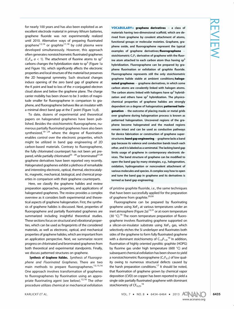
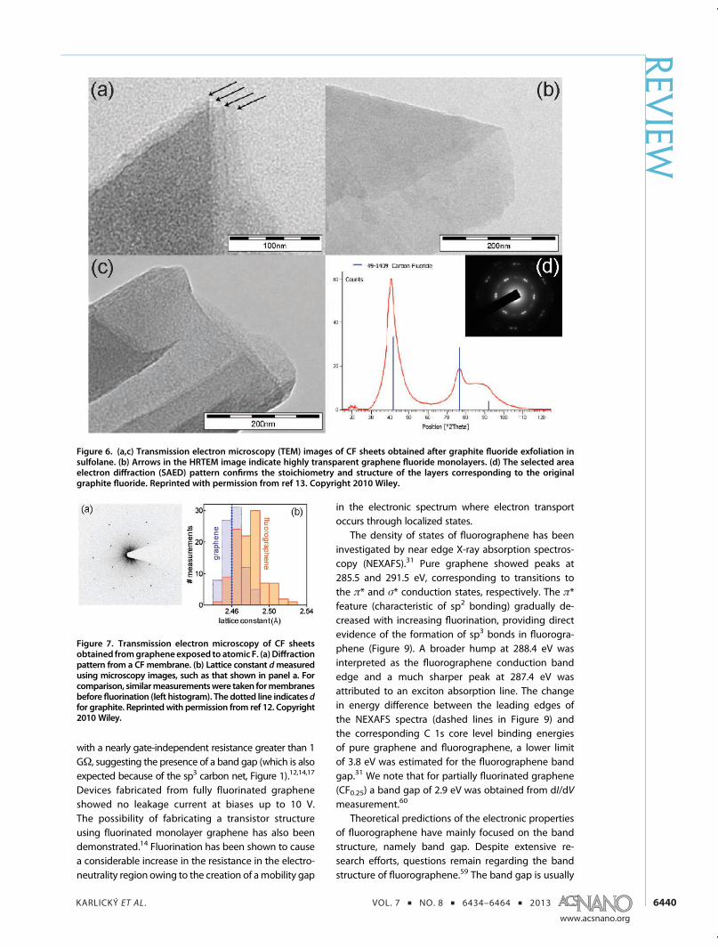
Electron diffraction analysis of fluorographene hasconfirmed the existence of a hexagonal crystallinestructure12,13,17 and stoichiometry13 equivalent tothat of graphite fluoride (Figure 6). It has been shownthat the retention of hexagonal crystalline order forfluorographene is similar to that of graphene with 1%expansion of the unit cell (Figure 7):12,17 compare theC1F1 experimental lattice constant of 2.48 Å versus 2.46Å for graphene. The increased unit cell and in-planelattice constant of CF is expected as the carbon atomsmaking C�C bonds are converted from a sp2 to sp3
configuration during the fluorination process accom-panied by an increase in the C�C bond length.The bonding and composition of fluorographenes hasalso been characterized by X-ray photoelectron spec-troscopy (XPS) and Raman spectroscopy. XPS analysisshowed the majority of bonding in this material is C�F(86%), with smaller fractions of C�F2 and C�F3 species(owing to defects at the free edges).16 These defectsare believed to originate during the graphene transferprocess and vary from one support to another; forexample, larger quantities of C�Fn (n > 1) specieswere observed for fluorinated graphene samples ona silicon-on-insulator substrate compared to those on
copper.16 Notably, the support also seems to affect thefluorine content. Early experiments suggested that thelateral dimensions of fluorographene sheets typicallyrange from 200 nm to 2 μm (see Figure 6).12,13
Definitive proof of the presence of fluorographenemonolayers has been obtained by atomic force micro-scopy (AFM) experiment (Figure 8), which revealed thatthe monolayer is 0.67�0.87 nm thick, although multi-layered sheets ca. 2�4 nm thick were also detected.13,17
Theexperimental values (allowing for theeffects of signalnoise and the presence of solvent impurities on thesurface or support), were in agreement with theoreticalestimates of the thickness of a single CF layer of 0.62 nmand were certainly less than the predicted thickness ofa two-layer graphene fluoride system of 1.24 nm.13
Electronic Properties of CF. The I�V characteristicsof fully fluorinated graphene are strongly nonlinear
Figure 5. (a) Honeycomb lattice structure of fluorogra-phene, made out of two interpenetrating triangular lattices(a1 and a2 are the lattice unit vectors, and δi, i= 1, 2, 3 are thenearest-neighbor vectors) (b) corresponding to the Brillouinzone, the reciprocal basis vectors and high-symmetrypoints Γ, M, and K. Reprinted with permission from ref 2.Copyright 2009 American Physical Society.
Figure 4. Four different configurations of fluorographene: (a) chair, (b) boat, (c) zigzag (stirrup), and (d) armchairconfigurations. The different colors (shades) represent fluorine atoms above and below the graphene plane. The supercellused to calculate the elastic constants is indicated by the dashedbox (see sections below). Reprintedwith permission from ref53. Copyright 2010 American Physical Society.
REVIEW
KARLICKÝ ET AL . VOL. 7 ’ NO. 8 ’ 6434–6464 ’ 2013
www.acsnano.org
6440
with a nearly gate-independent resistance greater than 1GΩ, suggesting the presence of a band gap (which is alsoexpected because of the sp3 carbon net, Figure 1).12,14,17
Devices fabricated from fully fluorinated grapheneshowed no leakage current at biases up to 10 V.The possibility of fabricating a transistor structureusing fluorinated monolayer graphene has also beendemonstrated.14 Fluorination has been shown to causea considerable increase in the resistance in the electro-neutrality region owing to the creation of amobility gap
in the electronic spectrum where electron transportoccurs through localized states.
The density of states of fluorographene has beeninvestigated by near edge X-ray absorption spectros-copy (NEXAFS).31 Pure graphene showed peaks at285.5 and 291.5 eV, corresponding to transitions tothe π* and σ* conduction states, respectively. The π*feature (characteristic of sp2 bonding) gradually de-creased with increasing fluorination, providing directevidence of the formation of sp3 bonds in fluorogra-phene (Figure 9). A broader hump at 288.4 eV wasinterpreted as the fluorographene conduction bandedge and a much sharper peak at 287.4 eV wasattributed to an exciton absorption line. The changein energy difference between the leading edges ofthe NEXAFS spectra (dashed lines in Figure 9) andthe corresponding C 1s core level binding energiesof pure graphene and fluorographene, a lower limitof 3.8 eV was estimated for the fluorographene bandgap.31 We note that for partially fluorinated graphene(CF0.25) a band gap of 2.9 eV was obtained from dI/dVmeasurement.60
Theoretical predictions of the electronic propertiesof fluorographene have mainly focused on the bandstructure, namely band gap. Despite extensive re-search efforts, questions remain regarding the bandstructure of fluorographene.59 The band gap is usually
Figure 6. (a,c) Transmission electron microscopy (TEM) images of CF sheets obtained after graphite fluoride exfoliation insulfolane. (b) Arrows in the HRTEM image indicate highly transparent graphene fluoride monolayers. (d) The selected areaelectron diffraction (SAED) pattern confirms the stoichiometry and structure of the layers corresponding to the originalgraphite fluoride. Reprinted with permission from ref 13. Copyright 2010 Wiley.
Figure 7. Transmission electron microscopy of CF sheetsobtained fromgraphene exposed to atomic F. (a) Diffractionpattern from a CFmembrane. (b) Lattice constant dmeasuredusing microscopy images, such as that shown in panel a. Forcomparison, similarmeasurementswere taken formembranesbefore fluorination (left histogram). The dotted line indicates dfor graphite. Reprinted with permission from ref 12. Copyright2010 Wiley.
REVIEW

KARLICKÝ ET AL . VOL. 7 ’ NO. 8 ’ 6434–6464 ’ 2013
www.acsnano.org
6441
considered for the chair conformation of fluorogra-phene with a unit cell containing four atoms (seeFigure 5 showing the unit cell and Brillouin zone).Traditional local density approximation (LDA) or gen-eralized gradient approximation (GGA) to DFT predictsthat fluorographene is a direct band gap material: thebottom of the conduction band and top of the valenceband are located at theΓpoint in the first Brillouin zone
(Figure 10). The top of the valence band is doublydegenerate and the maximum band gap is located atthe K points. The minimal direct band gap of fluoro-graphene of about 3.1 eV53,56�59,61�63 predicted fromGGA DFT indicates that fluorographene possessesinsulating properties, in agreement with early cal-culations on graphite fluoride.50,64 Band gap valuesof other fluorographene conformations (Figure 4) arerather similar or slightly higher up to 4.2 eV for thearmchair configuration.53,54 However, one main limita-tion of the DFT approach is it is an inherently ground-state theory. LDA and GGA functionals systematicallyunderestimate Kohn�Sham band gaps (comparedto experimentally determined values), whereas theHartree�Fock method systematically overestimatesthem. Hybrid functionals contain a fraction of Hartree�Fock exchange, and their computationally accessibleshort-range variants (as byHeyd, Scuseria, and Ernzerhof(HSE)65) are often effective for predicting band gapsof solids and low-dimensional carbon materials:66
the HSE06 functional67 predicts a band gap of about5 eV for fluorographene.58 The high-level many-bodyGW approximation (GWA), which includes electron�electron interactions beyond DFT, predicts a band gapof 7.0�8.3 eV53,54,56,59,68�70 (depending on GW leveland orbitals used),59 that is, around two times largerthan the value obtained with GGA DFT (Figure 10).Any agreement between GGA DFT and experimental“optical band gap” values (>3.0 or >3.8 eV, see below)is coincidental. On the other hand, accurate GWelectronic band gaps and the energies of electron
Figure 8. (a,b) Two independent AFM images of graphene fluoride monolayers and (c,d) their height profiles, providingevidence that the layers are <0.9 nm thick. Reprinted with permission from ref 13. Copyright 2010 Wiley.
Figure 9. NEXAFS spectra of pristine graphene and fluoro-graphene with two different fluorine contents. The dashedlines at 284.1 and 287.9 eVmark the leading edges of the π*resonance for the pristine and fluorinated sample, respec-tively. Reprinted from ref 31. Copyright 2011 AmericanChemical Society.
REVIEW

KARLICKÝ ET AL . VOL. 7 ’ NO. 8 ’ 6434–6464 ’ 2013
www.acsnano.org
6442
transitions derived from optical spectra do not exactlymatch each other, because the electron transitionsobserved in optical spectra involve formation of anexciton. Therefore DFT and GW band gaps shouldnot be directly compared with absorption peaks inoptical spectra and reasonable agreement with opticalmeasurement can be achieved only after inclusionof electron�hole correlations into calculations (seebelow for BSE�GWA spectra).59,70 Effect of variousdefects on discussed electronic properties is probablyrather small.59 GWApredicts that the band gapof fluoro-graphene is greater than that of graphane, whereasGGAfunctionals suggest the opposite trend. Recent calcula-tions have shown that it is possible to obtain the sameorder of band gaps with DFT as fromGW if the screenedhybrid functional HSE06 is used.58,59
Recently, spin�orbit couplings (SOCs) of fluorogra-phene have been calculated by DFT.61 The resultssuggested that SOC-induced band splittings near theirFermi energies in fluorographene are significantlyhigher (of the order of 10�2 eV) than for pure graphene(of the order of 10�6 eV) and are comparable to valuesfor diamond and archetypal semiconductors.61
Optical Properties of CF. Studies of the absorptionspectra of pristine, partially fluorinated or fully fluori-nated graphene have revealed that they exhibitdramatically different optical properties (Figure 11).Graphene shows an absorption spectrum that is rela-tively flat for light energies <2.5 eV but which stronglyincreases in the blue light region and has an absorptionpeak in the ultraviolet range (4.6 eV). In comparison,partially fluorinated graphene shows higher transpar-ency, whereas fluorographene appears to be transpar-ent at visible frequencies and only starts absorbinglight in the blue region (Figure 11).12 This provesthat fluorographene is a wide-gap semiconductor orinsulator with band gap g3.0 eV. Further, the absenceof Raman signatures confirms (virtually no sp2 coordi-nated carbon remains; see section 3.4. below) the
complete optical transparency of fully fluorinatedgraphene.12 Nair et al.12 have also studied fluorinatedgraphene laminates ofmacroscopic size (Figure 11). Thismaterial was found to be optically transparent with ayellowish color that corresponds to absorption in theviolet region. This provides direct visual evidence thatfluorographene is a wide-gap material. The light trans-mission spectra exhibited an onset at∼3.1 eV, in agree-ment with the gap value obtained from the absorptionspectra of individual fluorographene crystals.12
Photoluminescence measurements of fluorogra-phene dispersion in acetone have shown emissionpeaks at 3.8 and 3.65 eV (Figure 12).31 The former peakhas been assigned to band-to-band recombination offree electrons and holes because the same energy wasmeasured for the band gap of fluorographene by NEX-AFS. The 3.645 eV peak was 156meV (1260 cm�1) belowthe band gap emission, corresponding to the C�Fvibration mode. This feature was attributed to phonon-assisted radiative recombination across the band gap, forwhich the C�F vibration mode is excited when theelectron�hole pair recombines. With a lower degree of
Figure 10. Band structure of CF, togetherwith the orbital PDOSand total DOS. The LDAbandgap is shaded and zero energy isset to the Fermi level, EF. Valence and conduction band edges after GW0 correction are indicated by filled (red) circles.Reprinted with permission from ref 69. Copyright 2011 American Physical Society.
Figure 11. (a) Changes in optical transparency of graphenedue to fluorination. The solid curve is the absorptionbehavior expected for a 2D semiconductor with band gapof 3 eV. (b) Graphene paper before and after fluorination(left and right insets, respectively). The plot shows theoptical transparency of fluorographene paper as a functionof energy for a sample of 1 cm size and 5 μm thick in thephotograph. Reprinted with permission from ref 12. Copy-right 2010 Wiley.
REVIEW

KARLICKÝ ET AL . VOL. 7 ’ NO. 8 ’ 6434–6464 ’ 2013
www.acsnano.org
6443
fluorination (1dayoffluorination), an additional emissionpeak at 2.88 eV was observed, which was also accom-panied by a second peak located 157 meV (Figure 12).The optical band gap of fluorographene is nearly 3.8 eV,wide enough for optoelectronic applications in the blue/UV region.31
The first exciton peaks in the fluorographene ab-sorption spectrum have been predicted theoreticallyusing Bethe-Salpeter equation (BSE) on top of GWA,whichaccounts forelectron�electron (e�e)andelectron�hole (e�h) correlations, and compared with spectrafrom the random-phase approximation (RPA) on top ofGWA (without e�h).54,59,68,70 For the single-particleresult (Figure 13a, the blue curve, without e�h) theonset of the spectrum was located at the GWA bandgap and the absorption profile increased very slowlyuntil near 10 eV. This was interpreted as small spatialoverlapping of the wave functions of the valence bandmaximum (VBM) and the conduction band minimum(CBM), implying that the lowest optical transition fromVBM to the CBM (Figure 13b, transition v1�c1) is weak.The notable optical absorption starting from 10 eV wasmainly attributed to transitions from high energyvalence bands to the second conduction bands withenergies varying from 8 to 11 eV (Figure 13b, transi-tion v1�c2). When e�h interactions were taken intoaccount, a prominent peak was observed, which origi-nated from a few strong resonant excitonic states thatappeared at 9�10 eV54,59,68,70 (Figure 13a). The majorcontribution to this feature was related to transitionsfrom the top two valence bands and the lowest fourconduction bands (Figure 13b, two dominant transi-tions v1�c2 and v2�c1). In the low-frequency opticalabsorption spectrum, a bound exciton at 3.8 eV
(or alternatively 5.4 eV54 and 5.1 eV59,70) was identifiedwith a huge binding energy of 3.5 eV (or alternatively2 eV) and comparatively weak optical activity (inset ofFigure 13a). The large occupation probability associatedwith the low energy of this excitonic state suggests itmight play a vital role in the photoluminescence of thismaterial and explains the prominent ultraviolet lumi-nescence peak reported experimentally by Jeon et al.31
Vibrational Properties of CF. Theoretical analysisof vibrational modes can provide valuable insightsinto the experimental Raman and infrared spectra offluorographene CF. In particular, since Raman spectraconvey information on a particular structure, andhence can be viewed as its signature, observed peaksare compared to the calculated Raman-active modes.Theoretical analysis has revealed that the phononspectra and density of states (DOS) of the most stablechair conformation do not show clearly separatedgroups of phonons (Figure 14). The dominant contri-bution to the acoustic modes has been attributed tothe fluorine atoms, whereas the high-frequencymodesaround 1200 cm�1 have a clear carbon character.71
Twelve phonon modes of the chair conformation offluorographene, which has P3m1 symmetry (D3d pointgroup), have been shown to belong to four irreduciblerepresentations: Eg and A1g are Raman active modes,
Figure 12. Photoluminescence emission spectra recordedat room temperature (excitation at 290 nm, 4.275 eV) ofgraphene (blue) and fluorographene (green, 1 day fluorina-tion; red, 5 days). Reprinted from ref 31. Copyright 2011American Chemical Society.
Figure 13. (a) Optical absorption spectra of fluorographenewith (red line, BSE-GWA) or without e�h interactions (blueline, RPA-GWA). (b) GW band structure of fluorographene.Reprinted with permission from ref 68. Copyright 2011 TheMaterials Research Society.
REVIEW

KARLICKÝ ET AL . VOL. 7 ’ NO. 8 ’ 6434–6464 ’ 2013
www.acsnano.org
6444
while Eu and A2u are infrared active modes (Table 1).Some of the phonon branches of the CF boat con-formation have imaginary frequencies, and hence it ispredicted to be unstable in spite of the fact that such astructure can be optimized.69 However, the possibilitythat this unstable structure can occur at finite and smallsizes cannot be excluded.
Because Raman spectroscopy provides a wealth ofuseful information, it has been actively used during thefluorination process of graphene (Figure 15).12,14,16,17
However, because the energies of the lasers usedwere lower than the band gap (fluorographene iswide band gap material), no signature Raman activityfrom fully fluorinated regions was observed in thoseexperiments12,14,16 and the only Raman peaks wereassociated with graphene. The main features in theRaman spectra of pristine graphene are the G- and 2D-bands, which occur around 1580 and 2680 cm�1,respectively (Figure 15). The G-band is associated withthe doubly degenerate E2g phononmode of graphene,whereas the 2D mode (also called G0) originates froma second-order process, involving two phonons nearthe K point without the presence of any kind ofdisorders or defects. Conversely, the presence of de-fects in the sample activates additional peaks in theRaman spectra of graphene. The D, D0, and DþD0 peaksinvolve phonon modes from graphene, and henceoccur at the same frequencies in partially fluorinatedsamples (at 1350, 1620, and 2950 cm�1, respectively;Figure 15a).12,14,16 These Raman peaks originate fromdouble resonance processes at the K point in thepresence of defects. The D and G peaks of grapheneprovide valuable information on the density of defects.These peaks disappear for almost fully covered sam-ples, which has been found for fluorographene12,14,16
but not in previous experiments on graphane orgraphite fluorides.
The first report on Raman signatures of CF in thelow-frequency region by using a UV laser (with energyof 5.08 eV) was by Wang et al.18 Two Raman activemodes were detected at 1270 and 1345 cm�1, whichare absent under lower laser energies. Even thoughthe CF samples also contained multilayer regions, theexperimental values correlated with the aforemen-tionedDFT phonon frequencies (Figure 14): the higher-frequency mode as A1g mode with out-of-planemotions of F against C (at 1312 or 1305 cm�1)69,71
and the lower-frequency mode as a 2-fold degeneratein-plane Eg vibration (at 1244 or 1264 cm�1).69,71
FTIR spectra obtained in transmission mode(Figure 16a) have shown that fluorographene exhibitsmuch stronger IR bands than graphene due to thegreater transparency of the former.31 Furthermore, aprominent feature at 1260 cm�1 characteristic of cova-lent C�F bond stretching72 has been observed. Forfluorographene exfoliated by N-methyl-2-pyrrolidone(NMP), peaks at 1212 and 1084 cm�1 were observed
Figure 14. (a) Phonon dispersion of CF in the chair conformation and the corresponding phonon DOS. Reprinted withpermission from ref 71. Copyright 2011 American Institute of Physics. (b) Symmetries, frequencies, and descriptions ofRaman-active modes of CF. Reprinted with permission from ref 69. Copyright 2011 American Physical Society.
TABLE 1. List of Symmetries and Phonon Frequencies at
Different k-points for Fluorographene. R and I Indicate
Raman and Infrared Active Modes, Respectively71
symmetry (activity) Γ M K
A2u (R) 0 211 260Eu (I) 0 260 260Eu (I) 0 291 298Eg (R) 250 318 356Eg (R) 250 459 510Eu (I) 294 580 510Eu (I) 294 633 961A1g (R) 686 1039 962Eg (R) 1244 1106 962Eg (R) 1244 1116 1114A2u (I) 1219 1117 1114A1g (R) 1312 1188 1150
REVIEW

KARLICKÝ ET AL . VOL. 7 ’ NO. 8 ’ 6434–6464 ’ 2013
www.acsnano.org
6445
corresponding to the stretching vibration of the C�Fcovalent bonds and the semi-ionic stretching vibrationof C�F bonds, respectively (Figure 16b).23 Studies of FTIRspectra with increasing fluorination time (Figure 16c)have revealed an absorption band at 1112 cm�1 relatedto the 'semi-ionic' C�F, which gradually changes intoa strong band at 1211 cm�1 attributable to covalentC�F bonding.73 An experimental infrared active modeat 1204 cm�1 has also been reported.18 The aforemen-tioned frequencies of the experimental infrared activemode corresponding to C�F stretching agree with the
calculated infrared active mode A2u at the Γ point(at 1219 cm�1, Table 1).71
The experimental determination of the phonondispersion relations of fluorographene can be veryuseful in the characterization of thismaterial. As fluoro-graphene is a wide band gap material, this allowsdiscrimination of the Raman activity originating fromthe fully fluorinated regions during synthesis by using alaser with appropriate energies.71
Mechanical, Thermodynamical Properties and Stabi-
lity of CF. Graphene and its derivatives graphane and
Figure 15. Raman signatures of CF. (a) Evolution of the spectra for a graphenemembrane exposed to atomic F andmeasuredas a function of time under the same Raman conditions. The curves are shifted for clarity. (b) Intensities of the D and 2D peaks(normalized with respect to the G peak intensity) as a function of fluorination time. The solid curves are for guidance only.(c) Comparison of CFmembranes with graphite fluoride and its monolayer. Reprinted with permission from ref 12. Copyright2010 Wiley.
Figure 16. (a) FTIR spectra of CF prepared by fluorinating graphene, pristine graphene, and graphite fluoride. Reprinted fromref 31. Copyright 2011 American Chemical Society. (b) FTIR spectra of CF obtained at different sonication times for graphitefluoride exfoliatedbyNMP. Reprintedwith permission from ref 23. Copyright 2012Royal Society of Chemistry. (c) EvolutionofCF phases on graphenewith increasing exposure time to XeF2 characterized by FTIR spectra. Reprintedwith permission fromref 31. Copyright 2012 Wiley.
REVIEW

KARLICKÝ ET AL . VOL. 7 ’ NO. 8 ’ 6434–6464 ’ 2013
www.acsnano.org
6446
fluorographene can be isolated and made into free-hanging membranes. This makes it possible to mea-sure the elastic constants of these materials fromnanoindentation experiments by an atomic force mi-croscope. The experimental elastic constants can becompared to first-principles calculations, giving infor-mation about the purity and structural crystallinityof the experimental samples. Nair et al.12 have con-ducted a nanoindentation experiment on fluorogra-phene by recording the bending of an AFM cantileveras a function of its displacement, and hence calculatedthe force acting on the membrane (typical loadingcurves and breaking forces are shown in Figure 17),giving a value of 100( 30 N m1� or 0.3 TPa for the 2DYoung's modulus, (three times less stiff than graphenedue to the longer sp3 type bonds in CF). However, theexperimental Young'smodulus was approximately halfthe theoretical value (226 Nm�1).53 This was attributedto an appreciable number of defects in the experi-mental samples. Large scale atomistic simulationsusing the reactive force field approach have shown74
that fluorographene remains a flat sheet (unrippled)similar to graphane even at high temperature, that is,up to 900 K, in contrast to the thermal rippling behaviorof graphene.
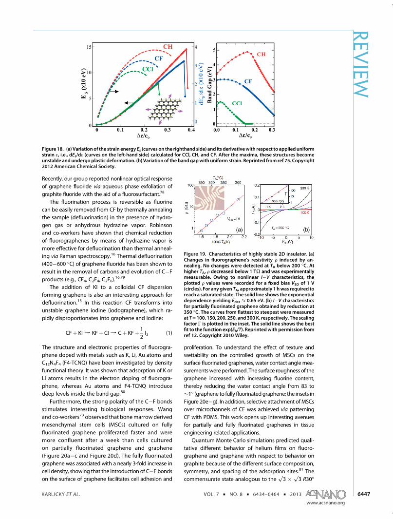
The variation of the strain energy, Es, and itsderivative with respect to the applied uniform strain,dEs/dε, have been predicted theoretically (Figure 18a;comparison with CH and CCl).75 The results showedthat the derivative was linear for small ε in the harmo-nic range. Elastic deformation continued until themaximum of dEs/dε, whereupon the structure revertedto its initial state when the applied strain was lifted.Beyond the maximum the structural instability sets inwith irreversible deformations. The region beyondthe maximum is called the plastic region. The effectof elastic strain on the band gap of CCl, CF, and CHwas also calculated, and the results are presented inFigure 18b. CH and CCl were predicted to have similar
response to elastic strain: their band gaps increasedfor small strain followed by a rapid decrease for largestrain. In contrast, the band gap of CF did not initiallyshow any significant increase with increasing strain: forsmall strain it was almost unaltered, but decreasedrapidly for large strain.
Superior nanoscale friction on fluorinated graphenehas been reported by Park et al.60,76 using ultrahighvacuum friction force microscopy. The measured fric-tion on fluorinated graphene with C4F compositionwas∼6 times larger than on pure graphene for appliednormal forces up to 150 nN, whereas fluorinationslightly reduced (by about 25%) the adhesion forcebetween the AFM tip and graphene.60 DFT calculationsconfirmed reduction of the adhesive properties andshowed friction force on graphene mainly governedby out-of-plane bending.76 In contrast, low interlayerfriction was reported for multilayer CF from dispersioncorrected DFT calculations.77
Electrical measurements (Figure 19) have beenutilized to study the thermal stability of CF in moredetail than possible with Raman spectroscopy.12 Thethermal stability of CF was observed to be higher thanthat of graphene, graphene oxide, and even graphitefluoride. Under similar conditions, graphite fluoridebegan decomposing at 300 �C. The higher stabilityof CF can be due to the absence of structural defectsand strain. The thermal stability and chemical inertnessof CFwas comparable to that of the fully fluorinated 1Dcarbon chain of Teflon.12,23 CF underwent slow decom-position at T > 260 �C and rapidly decomposed onlyabove 400 �C. These properties in principle makecolloidal CF derived from graphite fluoride a favorablecandidate to replace Teflon in various protective coat-ings. CF has also been shown to be resistant to varioussolvents under ambient conditions.
Chemistry of CF and Applications. Hydrophobic gra-phene fluoride (CF0.5) nanosheets can be made waterdispersible by stabilizing them with fluoro-surfactants.
Figure 17. Mechanical properties of CF. (a) Examples of the loading curves for graphene (blue) and CF (red) membranes.Fracture loads are marked by the circled crosses. Up until these breaking points, the curves were nonhysteretic. Top andbottom insets: AFM images of a CF membrane before and after its fracture, respectively. (b) Histogram of the breaking forcefor graphene (hashed) and CF (solid color). All the membranes (15 of each type) were mounted on identical Quantifoils andcontacted with the same AFM tip. Reprinted with permission from ref 12. Copyright 2010 Wiley.
REVIEW
KARLICKÝ ET AL . VOL. 7 ’ NO. 8 ’ 6434–6464 ’ 2013
www.acsnano.org
6447
Recently, our group reported nonlinear optical responseof graphene fluoride via aqueous phase exfoliation ofgraphite fluoride with the aid of a fluorosurfactant.78
The fluorination process is reversible as fluorinecan be easily removed from CF by thermally annealingthe sample (defluorination) in the presence of hydro-gen gas or anhydrous hydrazine vapor. Robinsonand co-workers have shown that chemical reductionof fluorographenes by means of hydrazine vapor ismore effective for defluorination than thermal anneal-ing via Raman spectroscopy.16 Thermal defluorination(400�600 �C) of graphene fluoride has been shown toresult in the removal of carbons and evolution of C�Fproducts (e.g., CF4, C2F4, C2F6).
16,79
The addition of KI to a colloidal CF dispersionforming graphene is also an interesting approach fordefluorination.13 In this reaction CF transforms intounstable graphene iodine (iodographene), which ra-pidly disproportionates into graphene and iodine:
CFþ KI f KFþ CI f Cþ KFþ 12I2 (1)
The structure and electronic properties of fluorogra-phene doped with metals such as K, Li, Au atoms andC12N4F4 (F4-TCNQ) have been investigated by densityfunctional theory. It was shown that adsorption of K orLi atoms results in the electron doping of fluorogra-phene, whereas Au atoms and F4-TCNQ introducedeep levels inside the band gap.80
Furthermore, the strong polarity of the C�F bondsstimulates interesting biological responses. Wangand co-workers73 observed that bonemarrow derivedmesenchymal stem cells (MSCs) cultured on fullyfluorinated graphene proliferated faster and weremore confluent after a week than cells culturedon partially fluorinated graphene and graphene(Figure 20a�c and Figure 20d). The fully fluorinatedgraphene was associated with a nearly 3-fold increase incell density, showing that the introduction of C�F bondson the surface of graphene facilitates cell adhesion and
proliferation. To understand the effect of texture andwettability on the controlled growth of MSCs on thesurface fluorinated graphenes, water contact anglemea-surementswereperformed. The surface roughnessof thegraphene increased with increasing fluorine content,thereby reducing the water contact angle from 83 to∼1� (graphene to fullyfluorinatedgraphene; the insets inFigure 20e�g). In addition, selective attachment ofMSCsover microchannels of CF was achieved via patterningCF with PDMS. This work opens up interesting avenuesfor partially and fully fluorinated graphenes in tissueengineering related applications.
Quantum Monte Carlo simulations predicted quali-tative different behavior of helium films on fluoro-graphene and graphane with respect to behavior ongraphite because of the different surface composition,symmetry, and spacing of the adsorption sites.81 Thecommensurate state analogous to the
√3 � √
3 R30�
Figure 18. (a) Variationof the strain energy Es (curves on the righthand side) and its derivativewith respect to applied uniformstrain ε, i.e., dEs/dε (curves on the left-hand side) calculated for CCl, CH, and CF. After the maxima, these structures becomeunstable andundergo plastic deformation. (b) Variation of the bandgapwith uniform strain. Reprinted from ref 75. Copyright2012 American Chemical Society.
Figure 19. Characteristics of highly stable 2D insulator. (a)Changes in fluorographene's resistivity F induced by an-nealing. No changes were detected at TA below 200 �C. Athigher TA, F decreased below 1 TΩ and was experimentallymeasurable. Owing to nonlinear I�V characteristics, theplotted F values were recorded for a fixed bias VSD of 1 V(circles). For anygiven TA, approximately 1 hwas required toreach a saturated state. The solid line shows the exponentialdependence yielding Edes ≈ 0.65 eV. (b) I�V characteristicsfor partially fluorinated graphene obtained by reduction at350 �C. The curves from flattest to steepest were measuredat T=100, 150, 200, 250, and 300K, respectively. The scalingfactor Γ is plotted in the inset. The solid line shows the bestfit to the function exp(Eh/T). Reprintedwith permission fromref 12. Copyright 2010 Wiley.
REVIEW

KARLICKÝ ET AL . VOL. 7 ’ NO. 8 ’ 6434–6464 ’ 2013
www.acsnano.org
6448
on graphite was unstable, while a superfluid groundstate for 4He and a fluid ground state for 3He werefound on fluorographene and graphane.
Fluorinated Graphenes. Basic Properties of Partially
Fluorinated Graphenes (C1Fn, n < 1). The introductionof fluorine modifies the electronic properties of gra-phene by reducing the charge in the conducting πorbitals.16,17 The resistance of the fluorinated gra-phenes can be tuned by the extent of fluorine content.For example, fluorinated graphene with a compositionof CF0.25 has been shown to have a 6-fold higherresistance than pristine graphene; in addition, CF0.25has been shown to be a wide band gap material thatexhibits optical transparency.16 Furthermore, defluor-ination of these samples either by heating or exposingto hydrazine vapors restored the conductivity andthe ambipolar nature similar to that of graphenes.For various applications related to the fabrication ofdevices, single-side fluorination of graphene would besufficient as it opens a significant band gap.20 Single-side fluorination can easily lead to a random surfacecoverage of up to CF0.5.
82 Band gaps of fluorinatedgraphenes (obtained by exfoliating graphite fluoridevia fluorinated ionic liquids) with compositions CF0.25and CF0.5 have been measured by diffuse reflectancespectroscopy as nearly 1.8 and 2.2 eV, respectively;19
however, a band gap of 2.9 eVwas obtained fromdI/dVmeasurement on CF0.25 (XeF2 fluorination of CVDgraphene as grown on a copper foil).60
From the theory, themost stable single-side confor-mation of C1Fa, where a < 1, is predicted to be CF0.25.
16
Density of states calculations for graphene with in-creasing F coverage showedwidening of the band gapand lowering of the Fermi level in the valence band.16
Tuning the band gap (ca. 0�3 eV at DFT level) canbe achieved by precise adsorption of fluorine as wellas a transformation from nonmagnetic semimetal(graphene) to either a nonmagnetic/magnetic metalor a magnetic/nonmagnetic semiconductor/insulatorwith a direct band gap.83 Band gaps of 2.93 eV(LDA) or 5.99 eV (GW0) for CF0.25 and 1.57 eV (LDA) or5.68 eV (GW0) for boat CF0.5 have been predicted(Figure 21a�c).69 In theoretical studies, the total en-ergies and/or binding energies have often been usedas criteria for whether a given CFn structure exists. Evenif a CFn structure seems to be in a minimum on thepotential energy surface, its stability should be meti-culously examined by calculating frequencies of allphonon modes in the Brillouin zone (BZ). Sahin et al.69
found that the CF0.25, the CF0.5 boat, and the CF0.5 chairstructures have positive frequencies throughout theBZ, indicating their stability. Optical absorption spectraof CF0.25 calculated from Bethe-Salpeter equation (BSE)have shown strong excitonic effects (analogically withCF, see subsection “Optical properties of CF” above).70
The first exciton peak locates at 4.21 eV (Figure 21d,black line); that is, the onset of absorption spectra issignificantly shifted to lower energies with respect to
Figure 20. (a�c) Fluorescent images of the actin cytoskeleton ofMSCs cultured on graphene, partially fluorinated graphene orfluorographene stained with rhodamine�phalloidin on day 7 (scale bar = 100 μm). (d) Proliferation of MSCs cultured on thegraphene films, showing the controlled growthofMSCs on fluorinated graphenewith different coverage offluorine. (e�g) AFMimages of graphene, partially fluorinated graphene, and fluorographene, respectively, showing the surface of fluorinatedgraphene (scale bar = 5 μm). The insets showdata for thewater contact angle. Reprintedwith permission from ref 73. Copyright2012 Wiley.
REVIEW

KARLICKÝ ET AL . VOL. 7 ’ NO. 8 ’ 6434–6464 ’ 2013
www.acsnano.org
6449
electronic GW band gap (6 eV69 from GW0, 5.5 eV70
fromG0W0). It is worth noting that large scale moleculardynamics simulations have shown a rolling of grapheneas a consequence of strain when graphene is fluori-nated/hydrogenated from a single side.84 Therefore, inthe absence of a substrate, free-standing single-sidedhalogenated graphene will not be a flat atomic layer.
Recently, fluorinated graphene obtained by coop-erative exfoliation of graphite fluoride using cetyl-trimethyl-ammonium bromide (CTAB) and dopaminehave been shown to exhibit a full-color emission fromviolet to red light (3.10�1.65 eV) when excited at365 nm.24 Band gap energies of fluorinated graphene(however, containing also oxygen) for several fluorinecoverages have beenmeasured (Figure 22).21 There is ablue shift observed for the fluorinated graphene sheetsas compared to that of graphene sheets (i.e., from269 nm of graphene to 251 and 247 nm in Figure 22a)indicating the opening of the band gap. Moreover, thehigher coverage of fluorine in graphene sheets de-creases the electrical conductivity (Figure 22b) andband gap widening (from 1.8 to 2.9 eV for CF0.10 andCF0.48, respectively) was observed (Figure 22c,d).
Fluorine-doped reduced graphene oxide (RGO)is reportedly a better substrate for surface enhancedRaman spectroscopy of molecules than unmodifiedRGO.33 In addition, it has been shown that the chemicalenhancement factor can be tuned by changing thefluorine/carbon ratio (17�27 atom %) due to the pre-sence of a strong local electric field induced by the localdipoles of F-containing groups on the RGO surface.33
Thomas et al.85 have reported that fluorinated grapheneoxide has high nonlinear absorption and nonlinear scat-tering, and its optical limiting threshold is about an orderof magnitude better than that of graphene oxide (GO).
Raman spectroscopy of fluorinated graphenes hasbeen mainly discussed in the fluorographene sec-tion. Single side fluorination leads to the appearanceof a D peak at 1350 cm�1 and broadening of theG (1580 cm�1) and D0 peaks (1620 cm�1), as well as adecrease in the 2D Raman peaks which is similarto that of graphene oxide.16 Sun and co-workers35
have studied layer-dependent fluorination of n-layergraphenes by SF6 plasma treatment. They observedthat fluorination of monolayer graphenes is easier andfaster than multilayer graphenes because of the form-er's high surface reactivity due to corrugations whichbecome notably smaller for bilayers and disappearfor thicker graphenes. During fluorination of mono-layer graphene, three new peaks at 1350, 1620, and2920 cm�1 were observed in the Raman spectra, whichwere ascribed to D, D0, and DþG bands, respectively.The presence of D, D0, and DþG bands indicates thatdefects were introduced into the graphene latticeduring the plasma treatment, which occurs more easilyfor single-layer graphene than thicker graphenes.The same group also observed that fluorination by
CF4 plasma treatment induces a lower number of latticedefects and higher magnitude of p-doping to graphenethan CHF3 plasma treatment.34
Other Unusual Properties of Fluorinated Graphenes
and Applications. Dilute fluorinated graphene sheets(F/C ratio of 1 to 2000or 0.05%) produced byCF4 plasmain a reactive ion etching system have been shown toexhibit anisotropic, colossal negative magnetoresis-tance and unusual “staircase” behavior at low tempera-tures (<5 K).86 The concentration and distribution ofF-adatoms on graphene was measured by Raman
Figure 21. Energy band structures of various stable CFnstructures, together with the orbital partial densities ofstates (DOS) and total DOS. The LDA band gaps are shadedand zero energy is set to the Fermi level, EF. The total DOS isscaled to 45%. Valence and conduction-band edges afterGW0 correction are indicated by filled (red) circles. (a) CF0.5chair structure. (b) CF0.5 boat structure. (c) CF0.25 structure.Reprinted with permission from ref 69. Copyright 2011American Physical Society. (d) Absorption spectra of C4Ffor light parallel to the surface plane (along x direction,see panel e) calculated with and without the considerationof electron�hole Coulomb interaction, that is, GWþBSEand GWþRPA, respectively. The inset is the absorptionspectrum of C4F for light polarization perpendicular tothe surface plane. Reprinted with permission from ref 70.Copyright 2013 American Physical Society.
REVIEW

KARLICKÝ ET AL . VOL. 7 ’ NO. 8 ’ 6434–6464 ’ 2013
www.acsnano.org
6450
spectroscopy and scanning tunneling microscopy (STM).The resistance at the charge neutrality point increased by3 orders of magnitude from 25 kΩ at 200 K to 2.5 MΩat 5 K, displaying a strong insulating behavior at dilute Fconcentration.86 Moreover, the presence of adatom-induced local magnetic moments has been reported indilute fluorinated graphene due to observed spin-flipscattering.87 The spin-flip rate was tunable via fluorinecoverage and carrier density. Modification of graphenewith fluorine may offer a platform for studying magnet-ism in this unusual two-dimensional electron gas anda gate-controllable, lithography-compatible, approachto control spins in graphene spintronics devices.
Diluted F atoms chemisorbed on graphene havealso been investigated theoretically.88 It was shownthat the nature of the chemical bonding of an F atomadsorbed on top of a C atom in graphene stronglydepends on carrier doping. In neutral samples, the Fimpurities make a sp3-like bonding of the C atombelow, generating a local deformation of the hexago-nal lattice. As the graphene is electron-doped, the Catom withdraws back to the graphene plane and forhigh doping its electronic structure corresponds to anearly pure sp2 configuration. This sp3�sp2 doping-induced crossover provides a new facility for control-ling graphene's electronic properties.
Fluorination of graphene has been shown to resultin the development of strong paramagnetism withincreasing fluorine coverages, that is, in CFx sampleswith x increasing from0.1 to 1 (fluorographene), as wellas more than an order of magnitude increase in low-Tsaturation magnetization (Figure 23a).89 For the stoi-chiometric fluorographene C1F1, a significant decreasein themagnetization was observed compared to CF0.75or CF0.9, even though the material showed strongparamagnetism. The number of spins N increasedmonotonically with x up to x ≈ 0.9, then decreasedslightly for the fully fluorinated samples (Figure 23b).A plot of the number of Bohr magnetons, μB, perattached F atom (inset in Figure 23b) clearly showedthat the initial increase (up to x ≈ 0.5) in the numberof paramagnetic centers was proportional to x, buta more complicated relation between the number ofatoms and N applied at higher x.
Recently, a method to obtain ultrathin, uniform,high-κ, and top-gate dielectrics required to realizethe full potential of graphene-based device technolo-gies was developed.37 A 15 nm atomic layer deposi-tion (ALS) Al2O3 was uniformly deposited on epitaxialgraphene functionalized by fluorine atoms. The under-lying graphene properties were not degraded, and 6.7%of the surface of epitaxial graphene was converted to
Figure 22. (a) UV�Visible absorption spectra of graphene oxide (GO), hydrothermally reduced graphene sheets (HGS), andtwo typical fluorinated graphene sheets (FGS) samples (FGS-150 and FGS-180). (b) Electrical conductivities of FGS samplesaccompanying the variation in C/F ratio. The inset shows a schematic model of the four-probe instrument used. (c) Arrheniusplot for the logarithm of conductivities of fluorinated graphenes series versus the inverse of temperature. (d) Experimentalband gap energies of fluorinated graphene (obtained from slopes of lines in panel c subplot) for several F coverages.Reprinted with permission from ref 21. Copyright 2012 Elsevier.
REVIEW

KARLICKÝ ET AL . VOL. 7 ’ NO. 8 ’ 6434–6464 ’ 2013
www.acsnano.org
6451
C�F bonds which provided enough ALD nucleationsites to obtain conformal films without pinholes.
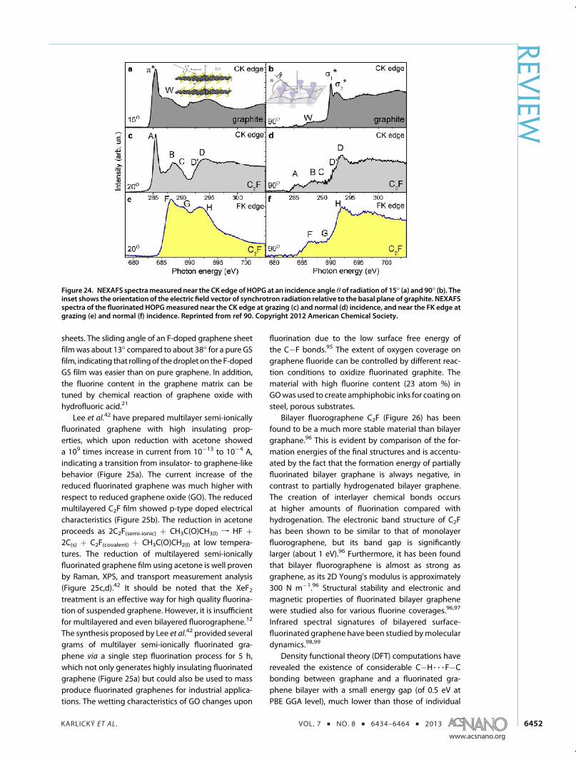
NEXAFS spectroscopy has been demonstrated tobe a powerful technique for evaluating the anisotropyin the chemical bonding of semifluorinated graphite(using a gaseous mixture of BrF3 and Br2).
90 The CKedge NEXAFS spectra of fluorinated HOPG measuredat incidence angles of 20� and 90� are compared inFigure 24. This figure shows that the π-system of C2Fis retained after fluorination, as seen from the intensepeak near 285 eV. The peak B at 288.5 eV with ashoulder C around 290 eV is related to 1s f σ* transi-tions within carbon atoms bonded with fluorine.All three peaks are significantly reduced in intensitywhen the spectra are recorded at normal incidence(Figure 24d), implying that these peaks (A, B, and C) are
largely due to carbon electrons from orbitals perpen-dicular to the basal plane. The intensity of D0 and Dare independent of the beam direction and are asso-ciatedwith transitions involving states of carbon atoms(σ* states) that are nonbonded or bondedwith fluorineatoms. The strong dependence of the intensity ofpeaks F and G (measured by FK edge spectra) on theincidence of X-ray radiation (Figure 24e and Figure 24f)shows that the C�F bonds have a predominantly per-pendicular orientation to the basal plane. This spectro-scopic technique helps to shed light on the anisotropicstructure of semifluorinated graphite, in which half thecarbon atoms are covalently bonded with fluorine, whilethe rest of the carbon atoms preserve π electrons.
The thermal conductivity of fluorinated graphenehas also been studied theoretically by classical none-quilibrium molecular dynamics.91 The thermal conduc-tivity was found to depend strongly on the coverageand distribution of fluorine atoms. For random fluorina-tion, the thermal conductivity decreased rapidly withincreasing fluorine coverage from 0 to 20%, stabilizedbetween 20 and 70%, and then increased rapidly as thecoverage approached 100%. The thermal conductivityof graphene fluoride was much less sensitive to tensilestrain than that of pristine graphene.
Monte Carlo calculations have suggested thatfluoro-graphenes reduce the binding energies of adsorbates(such as CH4,CO2, N2, O2, H2S, SO2) with respect to puregraphene.92 In most cases, the adsorption selectivitywas greatest for unmodified graphene surfaces andwasreduced by fluorination.92
The surface chemistry associated with CF4- andCl2-based inductively coupled plasma�reactive ionetching (ICP�RIE) of the 6H-SiC (0001) surface followedby thermal annealing at 970 �C has the potential toyield large area graphene-on-insulator films.93
On the basis of the partially fluorinated graphenewith composition CF0.25, a novel class of “acceptortype” fluoride intercalated graphite compounds hasbeen proposed.94 According to theoretical predictionsand experimental evidence, these types of compoundsexhibit significantly higher isosteric heats of adsorptionfor H2 than previously demonstrated for commonlyavailable, porous carbon-basedmaterials. The unusuallystrong interaction with H2 arises from the semi-ionicnature of the C�F bonds. Although high H2 storagecapacity (>4 wt %) at near-ambient temperatures maynot be feasible due to diminished heats of adsorption atvery high H2 densities, enhanced storage properties canbe envisaged by doping the graphitic host with appro-priate species (e.g., nitrogen) to promotemoreextensivecharge transfer from graphene to F� anions.
Multilayered FluorinatedGraphenes (CaFb, a < b). Yanet al.22 have shown that fluorine-doped multilayeredgraphene (10 wt %, ∼6.6 atom %, synthesized by arcdischarge process) sheets exhibit superhydrophobicproperties (CAg 150�) comparable to that of graphene
Figure 23. (a) Magnetic moment ΔM (after subtractinglinear diamagnetic background) as a function of the parallelfield strength H for different F/C ratios. (b) Main panel:number of spins N extracted from the fits in panel a as afunctionof the F/C ratio. The solid curve is for guidanceonly.Inset: the same N normalized to the concentration ofadatoms in each sample (μB/F atom is obtained by dividingthe number of moments N, assuming that each carries 1 μB,by the number of F atoms per g of fluorinated graphene).Error bars indicate the accuracy of determination of thefluorine concentrations. Reprintedwith permission from ref89. Copyright 2012 Nature Publishing Group.
REVIEW
KARLICKÝ ET AL . VOL. 7 ’ NO. 8 ’ 6434–6464 ’ 2013
www.acsnano.org
6452
sheets. The sliding angle of an F-doped graphene sheetfilmwas about 13� compared to about 38� for a pure GSfilm, indicating that rollingof thedroplet on theF-dopedGS film was easier than on pure graphene. In addition,the fluorine content in the graphene matrix can betuned by chemical reaction of graphene oxide withhydrofluoric acid.21
Lee et al.42 have prepared multilayer semi-ionicallyfluorinated graphene with high insulating prop-erties, which upon reduction with acetone showeda 109 times increase in current from 10�13 to 10�4 A,indicating a transition from insulator- to graphene-likebehavior (Figure 25a). The current increase of thereduced fluorinated graphene was much higher withrespect to reduced graphene oxide (GO). The reducedmultilayered C2F film showed p-type doped electricalcharacteristics (Figure 25b). The reduction in acetoneproceeds as 2C2F(semi‑ionic) þ CH3C(O)CH3(l) f HF þ2C(s) þ C2F(covalent) þ CH3C(O)CH2(l) at low tempera-tures. The reduction of multilayered semi-ionicallyfluorinated graphene film using acetone is well provenby Raman, XPS, and transport measurement analysis(Figure 25c,d).42 It should be noted that the XeF2treatment is an effective way for high quality fluorina-tion of suspended graphene. However, it is insufficientfor multilayered and even bilayered fluorographene.12
The synthesis proposed by Lee et al.42 provided severalgrams of multilayer semi-ionically fluorinated gra-phene via a single step fluorination process for 5 h,which not only generates highly insulating fluorinatedgraphene (Figure 25a) but could also be used to massproduce fluorinated graphenes for industrial applica-tions. The wetting characteristics of GO changes upon
fluorination due to the low surface free energy ofthe C�F bonds.95 The extent of oxygen coverage ongraphene fluoride can be controlled by different reac-tion conditions to oxidize fluorinated graphite. Thematerial with high fluorine content (23 atom %) inGOwas used to create amphiphobic inks for coating onsteel, porous substrates.
Bilayer fluorographene C2F (Figure 26) has beenfound to be a much more stable material than bilayergraphane.96 This is evident by comparison of the for-mation energies of the final structures and is accentu-ated by the fact that the formation energy of partiallyfluorinated bilayer graphane is always negative, incontrast to partially hydrogenated bilayer graphene.The creation of interlayer chemical bonds occursat higher amounts of fluorination compared withhydrogenation. The electronic band structure of C2Fhas been shown to be similar to that of monolayerfluorographene, but its band gap is significantlylarger (about 1 eV).96 Furthermore, it has been foundthat bilayer fluorographene is almost as strong asgraphene, as its 2D Young's modulus is approximately300 N m�1.96 Structural stability and electronic andmagnetic properties of fluorinated bilayer graphenewere studied also for various fluorine coverages.96,97
Infrared spectral signatures of bilayered surface-fluorinated graphene have been studied bymoleculardynamics.98,99
Density functional theory (DFT) computations haverevealed the existence of considerable C�H 3 3 3 F�Cbonding between graphane and a fluorinated gra-phene bilayer with a small energy gap (of 0.5 eV atPBE GGA level), much lower than those of individual
Figure 24. NEXAFS spectrameasured near the CK edge of HOPG at an incidence angle θ of radiation of 15� (a) and 90� (b). Theinset shows the orientation of the electric field vector of synchrotron radiation relative to the basal plane of graphite. NEXAFSspectra of the fluorinated HOPGmeasured near the CK edge at grazing (c) and normal (d) incidence, and near the FK edge atgrazing (e) and normal (f) incidence. Reprinted from ref 90. Copyright 2012 American Chemical Society.
REVIEW

KARLICKÝ ET AL . VOL. 7 ’ NO. 8 ’ 6434–6464 ’ 2013
www.acsnano.org
6453
graphane and fluorographene. The binding strengthof this bilayer can be significantly enhanced by anappropriate external electrical field. Changing the di-rection and strength of the electric field can effectivelymodulate the energy gap of the G/CF bilayer (0�3.0 eV)and correspondingly causes a semiconductor�metaltransition.100 In sharp contrast, the electronic propertiesof separated graphane or fluorographene monolayerare rather robust in response to an electric field withcorresponding negligible modulation of the bandstructures.
Halogenated Graphenes (CaXb, X = Cl, Br, I; a e b).Chlorographene. The fully chlorinated graphene(chlorographene, graphene chloride, or CCl) has beenbroadly theoretically discussed,13,56�59,75 but not yet
prepared. Thepristine parentmaterial, graphite chloride,is unstable at temperatures >0 �C, but stable at lowertemperatures;15 therefore it is reasonable to assume thatCCl is unstable under ambient conditions. On the otherhand, its instability has not yet been proven experimen-tally. Moreover, partially chlorinated graphene deriva-tives have been reported recently.25�28 However, thecoverageof chlorine atomswasmaximally up to30 atom% (CCl0.43). The stability of such compounds has beenconfirmed from room temperatures to 500 �C.28 There-fore, the existence of chlorographene is still uncertainand further experiments are needed to verify whetherCCl is stable at room temperature.
The lattice constant and C�C distance in the chairconformation of chlorographene (2.91 Å and 1.76 Å)
Figure 25. (a) I�V characteristics of multilayered semi-ionically fluorinated graphene films before and after reduction.(b) I�Vg characteristics of a corresponding FETdevice before (inset) and after the reductionprocess. (c) Plot showing variationof current on the reduction time. (d) Raman spectroscopy results according to the reduction time. Reprinted with permissionfrom ref 42. Copyright 2013 Wiley.
Figure 26. (a) Top and (b) side views of bilayer fluorographene. The carbon atoms in the two layers are shown in differentcolors for clarity, and the fluorine atoms are indicated by light green (open circleswith the smallest diameter). Reprinted fromref 96. Copyright 2012 American Chemical Society.
REVIEW
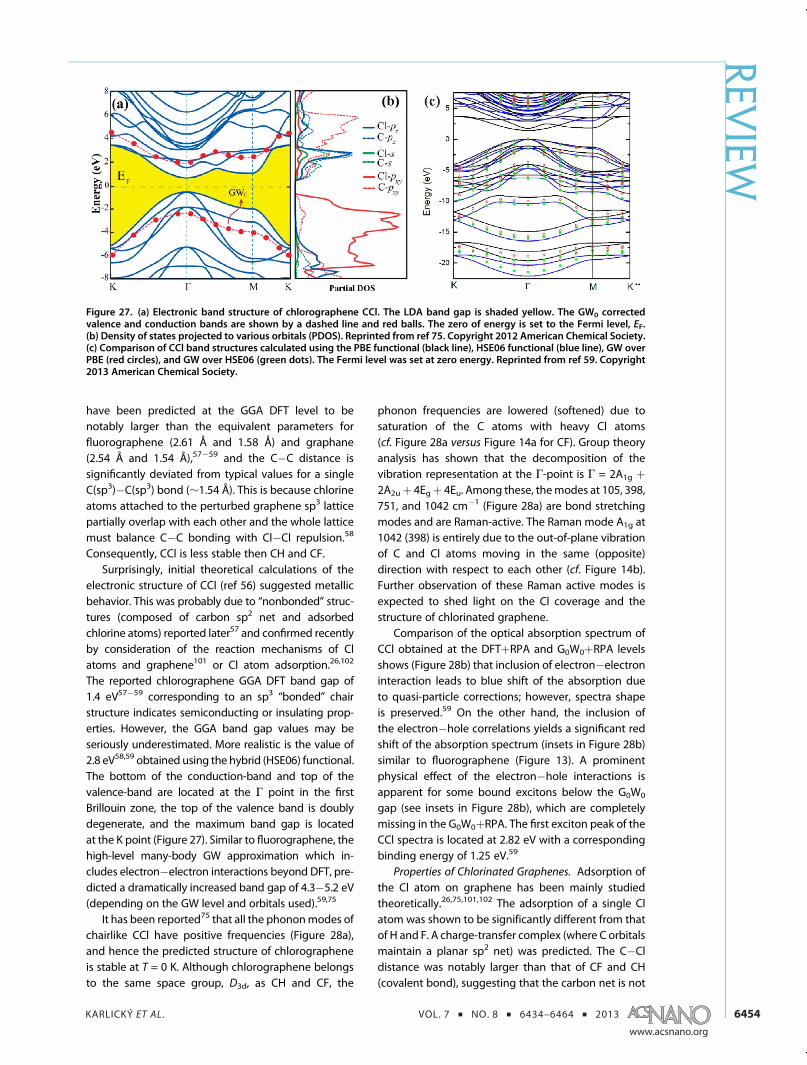
KARLICKÝ ET AL . VOL. 7 ’ NO. 8 ’ 6434–6464 ’ 2013
www.acsnano.org
6454
have been predicted at the GGA DFT level to benotably larger than the equivalent parameters forfluorographene (2.61 Å and 1.58 Å) and graphane(2.54 Å and 1.54 Å),57�59 and the C�C distance issignificantly deviated from typical values for a singleC(sp3)�C(sp3) bond (∼1.54 Å). This is because chlorineatoms attached to the perturbed graphene sp3 latticepartially overlap with each other and the whole latticemust balance C�C bonding with Cl�Cl repulsion.58
Consequently, CCl is less stable then CH and CF.Surprisingly, initial theoretical calculations of the
electronic structure of CCl (ref 56) suggested metallicbehavior. This was probably due to “nonbonded” struc-tures (composed of carbon sp2 net and adsorbedchlorine atoms) reported later57 and confirmed recentlyby consideration of the reaction mechanisms of Clatoms and graphene101 or Cl atom adsorption.26,102
The reported chlorographene GGA DFT band gap of1.4 eV57�59 corresponding to an sp3 “bonded” chairstructure indicates semiconducting or insulating prop-erties. However, the GGA band gap values may beseriously underestimated. More realistic is the value of2.8 eV58,59 obtained using the hybrid (HSE06) functional.The bottom of the conduction-band and top of thevalence-band are located at the Γ point in the firstBrillouin zone, the top of the valence band is doublydegenerate, and the maximum band gap is locatedat the K point (Figure 27). Similar to fluorographene, thehigh-level many-body GW approximation which in-cludes electron�electron interactions beyond DFT, pre-dicted a dramatically increased band gap of 4.3�5.2 eV(depending on the GW level and orbitals used).59,75
It has been reported75 that all the phononmodes ofchairlike CCl have positive frequencies (Figure 28a),and hence the predicted structure of chlorographeneis stable at T = 0 K. Although chlorographene belongsto the same space group, D3d, as CH and CF, the
phonon frequencies are lowered (softened) due tosaturation of the C atoms with heavy Cl atoms(cf. Figure 28a versus Figure 14a for CF). Group theoryanalysis has shown that the decomposition of thevibration representation at the Γ-point is Γ = 2A1g þ2A2uþ 4Egþ 4Eu. Among these, themodes at 105, 398,751, and 1042 cm�1 (Figure 28a) are bond stretchingmodes and are Raman-active. The Raman mode A1g at1042 (398) is entirely due to the out-of-plane vibrationof C and Cl atoms moving in the same (opposite)direction with respect to each other (cf. Figure 14b).Further observation of these Raman active modes isexpected to shed light on the Cl coverage and thestructure of chlorinated graphene.
Comparison of the optical absorption spectrum ofCCl obtained at the DFTþRPA and G0W0þRPA levelsshows (Figure 28b) that inclusion of electron�electroninteraction leads to blue shift of the absorption dueto quasi-particle corrections; however, spectra shapeis preserved.59 On the other hand, the inclusion ofthe electron�hole correlations yields a significant redshift of the absorption spectrum (insets in Figure 28b)similar to fluorographene (Figure 13). A prominentphysical effect of the electron�hole interactions isapparent for some bound excitons below the G0W0
gap (see insets in Figure 28b), which are completelymissing in the G0W0þRPA. The first exciton peak of theCCl spectra is located at 2.82 eV with a correspondingbinding energy of 1.25 eV.59
Properties of Chlorinated Graphenes. Adsorption ofthe Cl atom on graphene has been mainly studiedtheoretically.26,75,101,102 The adsorption of a single Clatom was shown to be significantly different from thatof H and F. A charge-transfer complex (where C orbitalsmaintain a planar sp2 net) was predicted. The C�Cldistance was notably larger than that of CF and CH(covalent bond), suggesting that the carbon net is not
Figure 27. (a) Electronic band structure of chlorographene CCl. The LDA band gap is shaded yellow. The GW0 correctedvalence and conduction bands are shown by a dashed line and red balls. The zero of energy is set to the Fermi level, EF.(b) Density of states projected to various orbitals (PDOS). Reprinted from ref 75. Copyright 2012 American Chemical Society.(c) Comparison of CCl band structures calculated using the PBE functional (black line), HSE06 functional (blue line), GW overPBE (red circles), and GW over HSE06 (green dots). The Fermi level was set at zero energy. Reprinted from ref 59. Copyright2013 American Chemical Society.
REVIEW
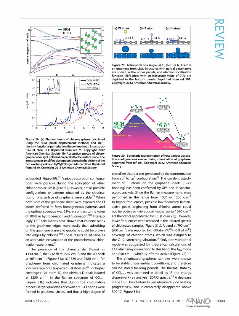
KARLICKÝ ET AL . VOL. 7 ’ NO. 8 ’ 6434–6464 ’ 2013
www.acsnano.org
6455
as buckled (Figure 29).101 Various adsorption configura-tions were possible during the adsorption of otherchlorinemolecules (Figure 30), However, not all possibleconfigurations or patterns obtained by the chlorina-tion of one surface of graphene were stable.75 Whenboth sides of the graphene sheet were exposed, the Clatoms preferred to form homogeneous patterns, andthe optimal coverage was 25%, in contrast to the valueof 100% in hydrogenation and fluorination.101 Interest-ingly, DFT calculations have shown that chlorine bindsto the graphene edges more easily than adsorbingon the graphene plane and graphene could be brokeninto edges by chlorine.102 Those results could serve asan alternative explanation of the photochemical chlor-ination experiment.25
The presence of the characteristic D-peak at1330 cm�1, the G-peak at 1587 cm�1, and the 2D-peakat 2654 cm�1 (Figure 31a; cf. 1580 and 2680 cm�1 forgraphene) from chlorinated graphene indicates alow coverage of Cl (expected∼8 atom%).25 For highercoverage (∼21 atom %), the obvious D peak locatedat 1359 cm�1 in the Raman spectrum of CCl0.21(Figure 31b) indicates that during the chlorinationprocess, larger quantities of covalent C�Cl bonds wereformed in graphene sheets, and thus a high degree of
crystalline disorder was generated by the transformationfrom sp2 to sp3 configuration.27 The covalent attach-ment of Cl atoms on the graphene sheets (C�Clbonding) has been confirmed by XPS and IR spectro-scopic analysis. Since the Raman measurements wereperformed in the range from 1000 or 1250 cm�1
to higher frequencies, possible low-frequency Raman-active peaks originating from chlorine atoms couldnot be observed (vibrational modes up to 1050 cm�1
are theoretically predicted for CCl (Figure 28)). However,lower frequencies were recorded in the infrared spectraof chlorinated samples (Figure 31c). A band at 790 cm�1
(930 cm�1) was reported for∼30 atom%28 (∼5.9 wt%48)coverage of chlorine atoms, which was assigned tothe C�Cl stretching vibration.28 Only one vibrationalmode was suggested by theoretical calculations ofCCl which may correspond to this band: the A2u modeat ∼850 cm�1, which is infrared active (Figure 28).75
The chlorinated graphene samples were shownto be stable under ambient conditions, and thereforecan be stored for long periods. The thermal stabilityof CCl0.43 was examined in detail by IR and energydispersive X-ray analysis (EDAX) spectra.28 A decreasein the C�Cl band intensity was observed upon heatingprogressively, and it completely disappeared above500 �C (Figure 31c).
Figure 28. (a) Phonon bands of chlorographene calculatedusing the SDM (small displacement method) and DFPT(density functional perturbation theory) methods. Inset: struc-ture of chair CCl. Reprinted from ref 75. Copyright 2012American Chemical Society. (b) Absorption spectra of chloro-graphene for lightpolarizationparallel to the surfaceplane. Theinsets containamplifiedabsorption spectra in the vicinityof thefirst exciton peak and G0W0(PBE) gap (dashed line). Reprintedfrom ref 59. Copyright 2013 American Chemical Society.
Figure 29. Adsorption of a single (a) Cl, (b) F, or (c) H atomon graphene from LDA. Structures with partial parametersare shown in the upper panels, and electron localizationfunction (ELF) plots with an isosurface value of 0.70 aredepicted in the bottom panels. Reprinted from ref 101.Copyright 2012 American Chemical Society.
Figure 30. Schematic representation of how various adsorp-tion configurations evolve during chlorination of graphene.Reprinted from ref 101. Copyright 2012 American ChemicalSociety.
REVIEW

KARLICKÝ ET AL . VOL. 7 ’ NO. 8 ’ 6434–6464 ’ 2013
www.acsnano.org
6456
The Cl coverage can be used to tune the grapheneband gap. Typically, the partially chlorinated grapheneexhibited a nonzero band gap and displayed a 4 ordersof magnitude higher sheet resistance than graphene(8% coverage of chlorine atoms).25 The higher resis-tance can be explained by perturbation of the gra-phene π-conjugated systems upon the chlorinationprocess. Furthermore, the dielectric constant (ε) of thechlorinated reduced graphene oxide composite film(ε = 169) was found to be much higher than untreatedreduced graphene oxide composite film (ε = 24).103
The large enrichment in the dielectric constant isattributed to the interfacial polarization between thechlorinated reduced graphene oxide platelets and thepolymer, along with the polar and polarizable C�Clbonds. These chlorinated reduced graphene oxideplatelets also displayed a 93% increase in conductivity,due to p-type doping effect created by Cl atoms.
Properties of Brominated Graphenes. Fully bromi-nated graphene (graphene bromide) is unstable, andmetallic behavior is predicted from calculations(Figure 32).56�58 The predicted lattice constant, C�C,and C�Br distances are 3.11, 1.86, and 1.92 Å, respec-tively, at the GGA DFT level.57 However, preparationsof a few-layer graphene brominated up to 4.8 atom %by UV irradiation in liquid-bromine medium28 andgraphene brominated up to 4 atom% usingmicrowave-spark assisted reaction27 have been reported. TheD peak (∼1350 cm�1) of brominated graphene(Figure 33a) has been shown to be weaker than thatof chlorinated graphene, possibly due to the lowerdegree of modification. Compared with the bandfor pristine graphene, the strong and symmetric 2Dpeak of CBr0.04 was blue-shifted (8 cm�1) and becamebroader, consistent with the small extent of modi-fication by Br27 The infrared spectrum of the bromi-nated graphene (9.9 wt %, 1.6 atom %) obtained fromthermally reduced graphene oxide (TRGO) showed avibration at 600 cm�1 (Figure 33b), which is indicativeof a C�Br bond in TRGO-Br.48
Changes in the electronic properties of few-layergraphenes doped by adsorption and intercalation of Br2vapors have been studied by Raman spectroscopy.104
The π conjugation network of graphene remainedunaffected after halogen doping. Adsorption of bro-mine on single-layer graphene created a high dopedhole density, well beyond that achieved by electricalgatingwith an ionic polymer electrolyte. In addition, the2D Raman band was completely quenched. The bilayerspectra indicated that doping by adsorbed Br2 wassymmetrical on the top and bottom layers. Br2 inter-calated into 3-layer and 4-layer graphenes. The combi-nation of both surface and interior doping with Br2 inthree and four layers created a relatively constantdoping level per layer. For graphene with three or morelayers, a resonant Raman signal was observed for Br2 ataround 238 cm�1; for monolayer and bilayer graphene,no bromine signal was observed (Figure 33c).104 Thiscould be an orientation effect, since, if the Br2 sitsperpendicular to the surface as LDA DFT calcula-tions suggest105 and orthogonal Raman is used, themolecules would be aligned with the beam and therewould be no interaction, and hence no signal. It hasbeen shown that the halogen molecule forms a Brþ þBr� pair, rendering it infrared active, and has an emptypz orbital located in the graphene electronic π cloud.105
Figure 31. (a) Raman spectra (wavelength λex = 632.8 nm) evolutionwith time for single-layer graphene reactedwith chlorineunder xenon lamp irradiation. Reprinted from ref 25. Copyright 2011 American Chemical Society. (b) Raman spectra ofchlorinated graphene prepared by microwave-spark (MiW-S) assisted reaction. Reprinted with permission from ref 27.Copyright 2012 Nature Publishing Group. (c) IR spectra of CClx heated for 4 h at various temperatures. Reprinted withpermission from ref 28. Copyright 2012 Royal Society of Chemistry.
Figure 32. Graphene bromide: band structure along thedirections joining somehigh symmetrypoints of theBrillouinzone and density of states. Reprinted with permission fromref 57. Copyright 2010 Institute of Physics.
REVIEW

KARLICKÝ ET AL . VOL. 7 ’ NO. 8 ’ 6434–6464 ’ 2013
www.acsnano.org
6457
Bromination opens a small band gap (∼86 meV at LDAlevel) and strongly dopes the graphene. The describedmolecule was identified as a new form of Br2 previouslyonly considered as an unstable intermediate of bro-mine-induced carbon-bond saturation.105
Iodine-Doped Graphene. Iodine-doped graphenescan be prepared by direct heating of camphor andI2 with an iodine loading of 3 atom %.46 In addition,exfoliation of graphene oxide and I2 under ultrasonictreatment followed by thermal annealing at varioustemperatures (500�1100 �C) generates iodine-dopedgraphenes (1.2�0.8 wt %; ∼0.1 atom %).47 Thesesamples showed good electrocatalytic activity andmethanol tolerance for the oxygen reduction reac-tion.47 X-ray photoelectron and Raman spectroscopicanalyses have confirmed the presence of elementaliodine in the form of triiodide (I3
�, peak at 117 cm�1)and pentaiodide (I5
�, peak at 154 cm�1) in these dopedsamples (Figure 34a),46,47 which is not surprisingas iodographene (fully iodinated graphene, grapheneiodide, CI) has been identified as an unstable andspontaneously decomposing compound.13 It is worthnoting that iodographene was identified as a meta-stable intermediate in the exchange reaction of eq 1in DMF as the solvent (in sulfolane, the considerablyfaster kinetics pass). The reaction occurs at just 150 �Cand the IR peak corresponding to the C�I unit(745 cm�1) was observed.13
Iodine doped graphene obtained from TRGO hasbeen shown to exhibit two additional peaks at approxi-mately 90 and 167 cm�1 that are absent in theRaman spectra of TRGO-Cl and TRGO-Br.48 The peakat 90 cm�1 was attributed to the presence of I3
� in thematerial, whereas the presence of I5
� gave rise to thepeak at 167 cm�1. The emergence of these peaksindicates the successful incorporation of iodine atomsinto the TRGO during the exfoliation procedure.
Jung and co-workers104 have studied changes in theelectronic properties of few-layer graphenes doped byadsorption and intercalation of I2 vapors by Ramanspectroscopy. The π conjugation network of graphene
remained unaffected after the halogen doping. In con-trast to Br2 (see above), the Raman G peak of three orfour layers with surface adsorbed I2 indicated that thehole doping density was larger on the surface layersthan on the interior layers and that I2 does not inter-calate into three or four layers. This adsorption-induceddifference between surface and interior layers impliedthat a bandgap opens in the bilayer-type bands of threeor four layers (Figure 34b). A comparison of possiblegraphene doping by adsorption and intercalation ofI2 with respect to Br2 is shown in the schematic diagramof Figure 34c.104
The interaction of various halogen molecules,such as ICl, Br2, IBr, and I2, with few-layer graphenehas been studied byGhosh et al.106 Halogenmolecules,being electron withdrawing in nature, induce dis-tinct changes in the electronic states of graphene,as evident by changes in the Raman and electronicabsorption spectroscopy. The magnitude of the mo-lecular charge-transfer between the halogens and thegraphenes varied in the order ICl > Br2 > IBr > I2.
Mixed Graphene Halides and Hybrids. In early calcu-lations on hydrogenated and halogenated graphenes,hypotheticalmixed structures C2HX (X= F, Cl, Br, I) werealso tested.56,57,107 Structures with H and X on differentsides of graphene were predicted to have a nonzeroband gap in the case of X = F, Cl (3.1 eV for C2HF and0.8 eV for C2HCl at GGA DFT level or 6.4 and 2.9 eV atG0W0 level, respectively),
56 whereas metallic behaviorwas predicted for heavier halogens (C2HBr and C2HI).Hybrid compounds C2LiF and C2LiH were reported asweak metal and semimetal, respectively. Very recently,a piezoelectric effect was predicted for six conforma-tions of different-side C2HF and C4HF compounds.108
Recently, hypothetic homogeneous-side mixed ha-lides have been suggested.58 All of the optimizedCaXbYc (X = H, F; Y = F, Cl, Br, I for Y 6¼ X) compoundswere considered and shown to be direct band gapmaterials. The results showed that the bottom ofthe conduction band and top of the valence bandare located at the Γ point in the first Brillouin zone for
Figure 33. (a) Raman spectra of brominated graphene prepared by microwave-spark (MiW-S)-assisted reaction. Reprintedwith permission from ref 27. Copyright 2012 Nature Publishing Group. (b) FTIR spectra of brominated graphene showingC�Br peak at 600 cm�1. Reprinted with permission from ref 48. Copyright 2013 Wiley. (c) Br2 stretching region of Ramanspectra for few-layer (L) graphenes exposed to bromine. The weak 303 cm�1 peak labeled Si is due to the underlyingcrystalline silicon substrate. The Br�Br peak near 240 cm�1 is due to intercalated bromine (see also scheme of Figure 34c).Reprinted from ref 104. Copyright 2009 American Chemical Society.
REVIEW

KARLICKÝ ET AL . VOL. 7 ’ NO. 8 ’ 6434–6464 ’ 2013
www.acsnano.org
6458
all CaXbYc species. The top of the valence band isdoubly degenerate and the maximum band gapsare located at the K points in CH, CF, CCl, and CBr.The band gap depends on the stoichiometry (chemicalcomposition) and can be relatively smoothly tunedfrom the maximal value in graphane to almost zero ingraphene bromide (Figure 35a). Even finer tuningcould in principle be achieved by adjusting the ratioof more than two substituents. Most of the consideredspecies appeared to have band gaps typical of in-sulators. Two species had band gaps comparable tothose of conventional semiconductors. Specifically, theband gaps of C2FBr and C2HBr were 1.32 and 1.55 eV(at HSE06 level), respectively. However, the latter isprobably unstable.
Stability of Halogenated Graphenes. The stability ofgraphene derivatives is usually assessed by consider-ing quantities such as the binding energy, energy offormation, or vibrational modes. All of the consideredmaterials are of similar type and stoichiometry, andtherefore it is possible to evaluate their stabilitythrough the following exchange reaction (for singlesupercells):13,58
aC2H2 þ bX2 þ cY2 þΔE0 T 2CaXbYc þ aH2 (2)
Here, the product CaXbYc (a = b þ c; X = H, F; Y = F, Cl,Br, I for Y 6¼ X) is the target material and ΔE0 is thedifference between the sums of the total energies ofthe products and the reactants. To compare the stabi-lity of different materials, it is better to consider thenormalized energy differenceΔE =ΔE0/(2a), where a isthe number of C atoms in a computational supercell.The choice of a reference material assigned with zeroΔE (and reactant in eq 2) is rather arbitrary, but a stableand experimentally prepared material is preferred. Ofthe two such available 2D graphene-based materials,graphane (CH) and fluorographene (CF), the formerwith lower stability is the better choice since it ispossible to obtain a simple indication of the stabilityfrom the ΔE value. If a CaXa‑cYc compound is more
stable than CH,ΔEwould be negative. A positive valueof ΔE indicates that the species is less stable than CHbut not necessarily thermodynamically unstable. Com-parison of ΔE values (Figure 35b) shows that the moststable of the graphene halide derivatives is fluorogra-phene. The decrease in stability on going from CF toCCl to CBr and finally to CI (which spontaneouslydecomposes to iodine and graphene13) is a conse-quence of the halogen atoms being forced into exces-sively close proximity by the graphene halide scaffold(Figure 36). The lower bound of stability is considered
Figure 35. Electronic band gaps (a) and stabilities (b) ofgraphene derivates CaXbYc, (a = b þ c) as a function of thestoichiometric ratiob:c for selected substituents X =H, F andY = F, Cl, Br, I calculated using the HSE06 functional. Thelimits of b:cf 0 [¥] correspond to CF, CCl, and CBr [CH andCF]. Reprinted with permission from ref 58. Copyright 2012American Institute of Physics.
Figure 34. (a) Raman spectra at lowwavenumbers showing formationof triiodide andpentaiodide in the graphene structure.Reprinted with permission from ref 46. Copyright 2011 Royal Society of Chemistry. (b) G peak Raman spectra of few-layergraphenes and graphite exposed to iodine vapor. The curves are vertically displaced. The relative intensity change from1 layer to graphite is shown. The G-peak of doped few-layer graphene samples is smaller than that of the 1580 cm�1 undopedgraphite G peak, as expected for doped samples. In graphite, a small peak at 1601 cm�1 may correspond to surface graphenelayers with adsorbed I2. (c) Schematic diagram of few-layer graphenes exposed to Br2 (left) and I2 (right). On the left side,the 3-layer and 4-layer structures have both intercalated (dark pink) and adsorbed (light pink) Br2 layers. On the right side, thethree-layer and four-layer structures have surface adsorbed (light blue) iodine anion layers without intercalation. Reprintedfrom ref 104. Copyright 2009 American Chemical Society.
REVIEW
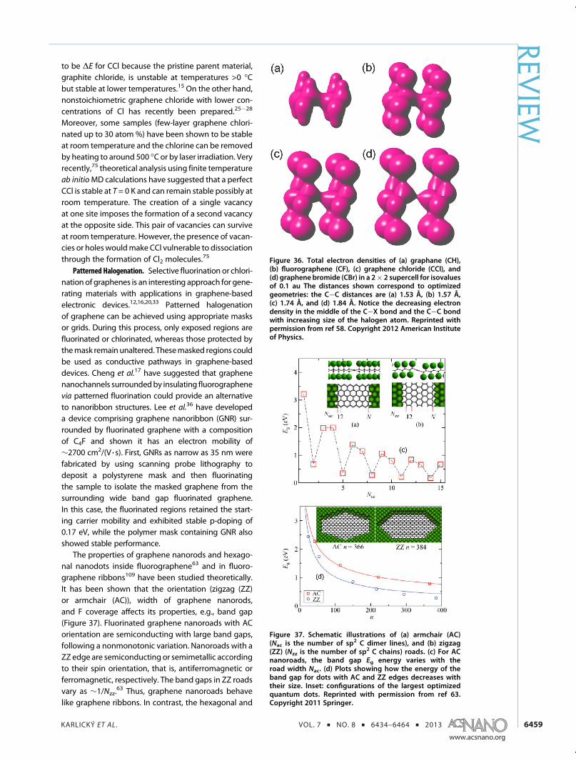
KARLICKÝ ET AL . VOL. 7 ’ NO. 8 ’ 6434–6464 ’ 2013
www.acsnano.org
6459
to be ΔE for CCl because the pristine parent material,graphite chloride, is unstable at temperatures >0 �Cbut stable at lower temperatures.15 On the other hand,nonstoichiometric graphene chloride with lower con-centrations of Cl has recently been prepared.25�28
Moreover, some samples (few-layer graphene chlori-nated up to 30 atom %) have been shown to be stableat room temperature and the chlorine can be removedby heating to around 500 �C or by laser irradiation. Veryrecently,75 theoretical analysis using finite temperatureab initioMD calculations have suggested that a perfectCCl is stable at T = 0 K and can remain stable possibly atroom temperature. The creation of a single vacancyat one site imposes the formation of a second vacancyat the opposite side. This pair of vacancies can surviveat room temperature. However, the presence of vacan-cies or holeswouldmake CCl vulnerable to dissociationthrough the formation of Cl2 molecules.75
Patterned Halogenation. Selective fluorination or chlori-nation of graphenes is an interesting approach for gene-rating materials with applications in graphene-basedelectronic devices.12,16,20,33 Patterned halogenationof graphene can be achieved using appropriate masksor grids. During this process, only exposed regions arefluorinated or chlorinated, whereas those protected bythemask remainunaltered. Thesemasked regions couldbe used as conductive pathways in graphene-baseddevices. Cheng et al.17 have suggested that graphenenanochannels surroundedby insulating fluorographenevia patterned fluorination could provide an alternativeto nanoribbon structures. Lee et al.36 have developeda device comprising graphene nanoribbon (GNR) sur-rounded by fluorinated graphene with a compositionof C4F and shown it has an electron mobility of∼2700 cm2/(V 3 s). First, GNRs as narrow as 35 nm werefabricated by using scanning probe lithography todeposit a polystyrene mask and then fluorinatingthe sample to isolate the masked graphene from thesurrounding wide band gap fluorinated graphene.In this case, the fluorinated regions retained the start-ing carrier mobility and exhibited stable p-doping of0.17 eV, while the polymer mask containing GNR alsoshowed stable performance.
The properties of graphene nanorods and hexago-nal nanodots inside fluorographene63 and in fluoro-graphene ribbons109 have been studied theoretically.It has been shown that the orientation (zigzag (ZZ)or armchair (AC)), width of graphene nanorods,and F coverage affects its properties, e.g., band gap(Figure 37). Fluorinated graphene nanoroads with ACorientation are semiconducting with large band gaps,following a nonmonotonic variation. Nanoroads with aZZ edge are semiconducting or semimetallic accordingto their spin orientation, that is, antiferromagnetic orferromagnetic, respectively. The band gaps in ZZ roadsvary as ∼1/Nzz.
63 Thus, graphene nanoroads behavelike graphene ribbons. In contrast, the hexagonal and
Figure 36. Total electron densities of (a) graphane (CH),(b) fluorographene (CF), (c) graphene chloride (CCl), and(d) graphene bromide (CBr) in a 2� 2 supercell for isovaluesof 0.1 au The distances shown correspond to optimizedgeometries: the C�C distances are (a) 1.53 Å, (b) 1.57 Å,(c) 1.74 Å, and (d) 1.84 Å. Notice the decreasing electrondensity in the middle of the C�X bond and the C�C bondwith increasing size of the halogen atom. Reprinted withpermission from ref 58. Copyright 2012 American Instituteof Physics.
Figure 37. Schematic illustrations of (a) armchair (AC)(Nac is the number of sp2 C dimer lines), and (b) zigzag(ZZ) (Nzz is the number of sp2 C chains) roads. (c) For ACnanoroads, the band gap Eg energy varies with theroad width Nac. (d) Plots showing how the energy of theband gap for dots with AC and ZZ edges decreases withtheir size. Inset: configurations of the largest optimizedquantum dots. Reprinted with permission from ref 63.Copyright 2011 Springer.
REVIEW

KARLICKÝ ET AL . VOL. 7 ’ NO. 8 ’ 6434–6464 ’ 2013
www.acsnano.org
6460
triangular patterned vacancies in the fluorographenestructure have been shown to behave like quantumdots.63,110 Nonetheless, the presented properties arenot an unique feature for halogenated graphenestructures because similar behavior was reportedfor graphene nanorods111 or nanoribbons112,113 andhexagonal nanodots inside graphane.114 Graphenenanoribbons with various degree of fluorination upto full fluorination (i.e., rather an inverse system tothe previously mentioned graphene nanoroads insidefluorographene, however, with the same interfacesgraphene/fluorographene) were also studied. Bothfully fluorinated ZZ and AC graphene nanoribbonswere predicted to be semiconductors with width-dependent energy gaps.115 ZZ hybrid nanoribbonswith an F-terminated edge in the antiferromagneticstate were shown to be half-semiconductors, in whichthe spin degeneracy near the Fermi level was comple-tely broken. In contrast, hybrid armchair nanoribbonswere suggested to be nonmagnetic semiconductors.Interestingly, the results suggested that the electronicproperties of partially fluorinated ZZ graphene nano-ribbons could be finely tuned by edge chemical
modification and control of the width of fluorinatedgraphene.115
Later, it was shown that the resistivity of insulatingfluorinated graphenes can be progressively decreasedby several orders of magnitude simply by elec-tron beam irradiation.116 The electron-irradiated fluori-nated graphene ultimately exhibited a similar resis-tance per square to that of pristine graphene. Thedecrease in resistivity was attributed to fragmentationof C�F bonds induced by electron irradiation. Resultsshowed that standard electron beam patterningprocesses can be used to engineer conductive andsemiconductive structures with sizes ranging from afew micrometers down to a few tens of nanometers.This opens up new avenues for the fabrication ofgraphene-based transparent and flexible electronicdevices, with defluorinated graphene channels thatcan be used as metallic interconnects or elements ofdevice structures. Furthermore, patterning channelswith different conductivities may lead to the devel-opment of novel resistive memory and data storagedevices, with multiple byte levels associated withdifferent resistivities.
Figure 38. (a) Partially covered graphene derivative C(CN)0.25. (b) Fully covered graphene derivative COCN.
REVIEW

KARLICKÝ ET AL . VOL. 7 ’ NO. 8 ’ 6434–6464 ’ 2013
www.acsnano.org
6461
Conclusion and Future Challenges. This review showsthat stoichiometric fluorographene is already, togetherwith graphane and graphene oxide, a well-establishedmember of the family of graphene derivatives with broadapplication potential. Nevertheless, there are still somediscrepancies related to hydrophobicity/hydrophilicity offluorographene or to its exact band gap value. Despite ofa hugeprogress in researchof other partially halogenatedand mixed graphene halides, there are many challengesrelated to the controlled synthesis, properties, and bandgap engineering of these structures. No doubt, newstraightforward methods for the preparation of varioushalogenatedandmixedhalogenatedgraphenes are likelyto be developed in the near future.
One of important challenges include the synthesisand complex analysis of “pseudohalides”, at leastC�CN (Figure 38a) and C�OCN (Figure 38b). Similarly,substitution of halogen atoms by suitable functionalgroups would bring a high additional value for chemi-cal and sensing application; the same situation isexpected in the case of functionalization throughorganometallics, R�Mg�X. Concerning challenges inthe field of applications of graphene halides, colloidalfluorographenes are promising materials for the de-sign of novel polymer nanocomposites and protectivecoatings. Moreover, interesting electronic and trans-port properties may arise due to stacking of fluoro-graphenes/graphene or graphene/fluorographene/graphene (G/CF/G), which would act as nanocapacita-tors analogous to G/BN/G. Halogenated and stackedgraphenes can also be utilized for storing/adsorptionof important gases, for example, hydrogen storage.We envisage a great potential for the halogenatedgraphenes also in the fields of optics, biology, orelectrochemistry. This large scale of applications wouldbe even enlarged in the future also with respect to theexpected new kinds of graphene halides. This is, forexample, the case of recently developed fluorinatedgraphene quantum dots (F-GQDs) exhibiting brightblue photoluminescence and a clear upconversionphotoluminescence.117 Similarly, Janus-like asym-metric graphenes produced by cografting of halo-gens would find applications as novel sensors,actuators, and surfactants because of their interest-ing surface properties.118
Conflict of Interest: The authors declare no competingfinancial interest.
Acknowledgment. The authors acknowledge support bythe Operational Program Research and Development forInnovations;European Regional Development Fund (CZ.1.05/2.1.00/03.0058 of the Ministry of Education, Youth and Sportsof the Czech Republic), the Operational Program Educationfor Competitiveness;European Social Fund (CZ.1.07/2.3.00/20.0017 of the Ministry of Education, Youth and Sports ofthe Czech Republic), and the Czech Science Foundation(P208/12/G016). K.K.R. Datta acknowledges financial supportby the Operational Program Education for Competitiveness;European Social Fund (project CZ.1.07/2.3.00/30.0041 ofthe Ministry of Education, Youth and Sports of the CzechRepublic).
REFERENCES AND NOTES1. Novoselov, K. S.; Fal'ko, V. I.; Colombo, L.; Gellert, P. R.;
Schwab, M. G.; Kim, K. A Roadmap for Graphene. Nature2012, 490, 192–200.
2. Castro Neto, A. H.; Guinea, F.; Peres, N. M. R.; Novoselov,K. S.; Geim, A. K. The Electronic Properties of Graphene.Rev. Mod. Phys. 2009, 81, 109–162.
3. Schwierz, F. Graphene Transistors. Nat. Nanotechnol.2010, 5, 487–496.
4. Georgakilas, V.; Otyepka, M.; Bourlinos, A. B.; Chandra, V.;Kim, N.; Kemp, K. C.; Hobza, P.; Zboril, R.; Kim, K. S.Functionalization of Graphene: Covalent and Noncova-lent Approaches, Derivatives and Applications. Chem.Rev. 2012, 112, 6156–6214.
5. Ivanovskii, A. L. Graphene-Based and Graphene-likeMaterials. Russ. Chem. Rev. 2012, 81, 571–605.
6. Johns, J. E.; Hersam, M. C. Atomic Covalent Functionali-zation of Graphene. Acc. Chem. Res. 2013, 46, 77–86.
7. Zhang, T.; Xue, Q. Z.; Zhang, S.; Dong, M. D. TheoreticalApproaches to Graphene and Graphene-Based Materi-als. Nano Today 2012, 7, 180–200.
8. Sluiter, M. H. F.; Kawazoe, Y. Cluster Expansion Methodfor Adsorption: Application to Hydrogen Chemisorptionon Graphene. Phys. Rev. B 2003, 68, 085410.
9. Sofo, J. O.; Chaudhari, A. S.; Barber, G. D. Graphane:A Two-Dimensional Hydrocarbon. Phys. Rev. B 2007,75, 153401.
10. Ryu, S.; Han, M. Y.; Maultzsch, J.; Heinz, T. F.; Kim, P.;Steigerwald, M. L.; Brus, L. E. Reversible Basal PlaneHydrogenation of Graphene. Nano Lett. 2008, 8, 4597–4602.
11. Elias, D. C.; Nair, R. R.; Mohiuddin, T. M. G.; Morozov, S. V.;Blake, P.; Halsall, M. P.; Ferrari, A. C.; Boukhvalov, D. W.;Katsnelson, M. I.; Geim, A. K.; et al. Control of Graphene'sProperties by Reversible Hydrogenation: Evidence forGraphane. Science 2009, 323, 610–613.
12. Nair, R. R.; Ren, W. C.; Jalil, R.; Riaz, I.; Kravets, V. G.; Britnell,L.; Blake, P.; Schedin, F.; Mayorov, A. S.; Yuan, S. J.; et al.Fluorographene: A Two-Dimensional Counterpart ofTeflon. Small 2010, 6, 2877–2884.
13. Zboril, R.; Karlicky, F.; Bourlinos, A. B.; Steriotis, T. A.;Stubos, A. K.; Georgakilas, V.; Safarova, K.; Jancik, D.;Trapalis, C.; Otyepka, M. Graphene Fluoride: A StableStoichiometric Graphene Derivative and Its ChemicalConversion to Graphene. Small 2010, 6, 2885–2891.
14. Withers, F.; Dubois, M.; Savchenko, A. K. Electron Proper-ties of Fluorinated Single-Layer Graphene Transistors.Phys. Rev. B 2010, 82, 073403.
15. Rüdorff, W. Graphite Intercalation Compounds. In Adv.Inorg. Chem. Radiochem; Emcleus, J., Sharpe, A. G., Eds.;Academic Press: New York, 1959; Vol. 1, pp 223�266.
16. Robinson, J. T.; Burgess, J. S.; Junkermeier, C. E.; Badescu,S. C.; Reinecke, T. L.; Perkins, F. K.; Zalalutdniov, M. K.;Baldwin, J. W.; Culbertson, J. C.; Sheehan, P. E.; et al.Properties of Fluorinated Graphene Films. Nano Lett.2010, 10, 3001–3005.
17. Cheng, S.-H.; Zou, K.; Okino, F.; Gutierrez, H. R.; Gupta, A.;Shen, N.; Eklund, P. C.; Sofo, J. O.; Zhu, J. Reversible Fluori-nation of Graphene: Evidence of a Two-DimensionalWideBandgap Semiconductor. Phys. Rev. B 2010, 81, 205435.
18. Wang, B.; Sparks, J. R.; Gutierrez, H. R.; Okino, F.; Hao, Q. Z.;Tang, Y. J.; Crespi, V. H.; Sofo, J. O.; Zhu, J. Photolumines-cence From Nanocrystalline Graphite Monofluoride.Appl. Phys. Lett. 2010, 97, 141915.
19. Chang, H. X.; Cheng, J. S.; Liu, X. Q.; Gao, J. F.; Li, M. J.; Li,J. H.; Tao, X. M.; Ding, F.; Zheng, Z. J. Facile Synthesis ofWide-Bandgap Fluorinated Graphene Semiconductors.Chem.;Eur. J. 2011, 17, 8896–8903.
20. Lee, W. H.; Suk, J. W.; Chou, H.; Lee, J. H.; Hao, Y. F.; Wu,Y. P.; Piner, R.; Aldnwande, D.; Kim, K. S.; Ruoff, R. S.Selective-Area Fluorination of Graphene with Fluoro-polymer and Laser Irradiation. Nano Lett. 2012, 12, 2374–2378.
21. Wang, Z.; Wang, J.; Li, Z.; Gong, P.; Liu, X.; Zhang, L.; Ren, J.;Wang, H.; Yang, S. Synthesis of Fluorinated Graphene
REVIEW

KARLICKÝ ET AL . VOL. 7 ’ NO. 8 ’ 6434–6464 ’ 2013
www.acsnano.org
6462
with Tunable Degree of Fluorination. Carbon 2012, 50,5403–5410.
22. Shen, B. S.; Chen, J. T.; Yan, X. B.; Xue, Q. J. Synthesis ofFluorine-Doped Multi-layered Graphene Sheets by Arc-Discharge. RSC Adv. 2012, 2, 6761–6764.
23. Gong, P. W.; Wang, Z. F.; Wang, J. Q.; Wang, H. G.; Li, Z. P.;Fan, Z. J.; Xu, Y.; Han, X. X.; Yang, S. R. One-Pot Sono-chemical Preparation of Fluorographene and SelectiveTuning of Its Fluorine Coverage. J. Mater. Chem. 2012, 22,16950–16956.
24. Wang, Z.; Wang, J.; Li, Z.; Gong, P.; Ren, J.; Wang, H.;Han, X.; Yang, S. Cooperatively Exfoliated FluorinatedGraphene with Full-Color Emission. RSC Adv. 2012, 2,11681–11686.
25. Li, B.; Zhou, L.; Wu, D.; Peng, H. L.; Yan, K.; Zhou, Y.; Liu, Z. F.Photochemical Chlorination of Graphene. ACS Nano2011, 5, 5957–5961.
26. Wu, J.; Xie, L. M.; Li, Y. G.; Wang, H. L.; Ouyang, Y. J.; Guo, J.;Dai, H. J. Controlled Chlorine Plasma Reaction for Non-invasive Graphene Doping. J. Am. Chem. Soc. 2011, 133,19668–19671.
27. Zheng, J.; Hong-Tao, Liu; Bin, Wu; Chong-An, Di;Yun-Long, Guo; Ti, Wu; Gui, Yu; Liu, Y.-Q.; Zhu, D.-B.Production of Graphite Chloride and Bromide UsingMicrowave Sparks. Sci. Rep. 2012, 2, 662.
28. Gopalakrishnan, K.; Subrahmanyam, K. S.; Kumar, P.;Govindaraj, A.; Rao, C. N. R. Reversible Chemical Storageof Halogens in Few-Layer Graphene. RSC Adv. 2012, 2,1605–1608.
29. Novoselov, K. S.; Geim, A. K.; Morozov, S. V.; Jiang, D.;Zhang, Y.; Dubonos, S. V.; Grigorieva, I. V.; Firsov, A. A.Electric Field Effect in Atomically Thin Carbon Films.Science 2004, 306, 666–669.
30. Novoselov, K. S.; Jiang, D.; Schedin, F.; Booth, T. J.;Khotkevich, V. V.; Morozov, S. V.; Geim, A. K. Two-Dimensional Atomic Crystals. Proc. Natl. Acad. Sci. U.S.A. 2005, 102, 10451–10453.
31. Jeon, K. J.; Lee, Z.; Pollak, E.; Moreschini, L.; Bostwick, A.;Park, C. M.; Mendelsberg, R.; Radmilovic, V.; Kostecki, R.;Richardson, T. J.; et al. Fluorographene: A Wide BandgapSemiconductor with Ultraviolet Luminescence. ACSNano 2011, 5, 1042–1046.
32. Bourlinos, A. B.; Safarova, K.; Siskova, K.; Zboril, R. TheProduction of Chemically Converted Graphenes fromGraphite Fluoride. Carbon 2012, 50, 1425–1428.
33. Yu, X. X.; Lin, K.; Qiu, K. Q.; Cai, H. B.; Li, X. J.; Liu, J. Y.; Pan,N.; Fu, S. J.; Luo, Y.; Wang, X. P. Increased ChemicalEnhancement of Raman Spectra for Molecules Adsorbedon Fluorinated Reduced Graphene Oxide. Carbon 2012,50, 4512–4517.
34. Chen, M. J.; Zhou, H. Q.; Qiu, C. Y.; Yang, H. C.; Yu, F.; Sun,L. F. Layer-Dependent Fluorination and Doping of Gra-phene via Plasma Treatment. Nanotechnology 2012, 23,115706.
35. Yang, H. C.; Chen, M. J.; Zhou, H. Q.; Qiu, C. Y.; Hu, L. J.; Yu,F.; Chu, W. G.; Sun, S. Q.; Sun, L. F. Preferential andReversible Fluorination of Monolayer Graphene. J. Phys.Chem. C 2011, 115, 16844–16848.
36. Lee, W. K.; Robinson, J. T.; Gunlycke, D.; Stine, R. R.;Tamanaha, C. R.; King, W. P.; Sheehan, P. E. ChemicallyIsolated Graphene Nanoribbons Reversibly Formed inFluorographene Using Polymer Nanowire Masks. NanoLett. 2011, 11, 5461–5464.
37. Wheeler, V.; Garces, N.; Nyakiti, L.; Myers-Ward, R.;Jernigan, G.; Culbertson, J.; Eddy, C.; Gaskill, D. K. FluorineFunctionalization of Epitaxial Graphene for UniformDeposition of Thin High-Kappa Dielectrics. Carbon2012, 50, 2307–2314.
38. Tahara, K.; Iwasaki, T.; Matsutani, A.; Hatano, M. Effect ofRadical Fluorination on Mono- and Bi-layer Graphene inAr/F-2 Plasma. Appl. Phys. Lett. 2012, 101, 163105.
39. Sherpa, S. D.; Paniagua, S. A.; Levitin, G.; Marder, S. R.;Williams, M. D.; Hess, D. W. Photoelectron SpectroscopyStudies of Plasma-Fluorinated Epitaxial Graphene. J. Vac.Sci. Technol. B 2012, 30, 03D102.
40. Fedorov, V. E.; Grayfer, E. D.; Makotchenko, V. G.;Nazarov, A. S.; Shin, H. J.; Choi, J. Y. Highly ExfoliatedGraphite Fluoride as a Precursor for Graphene FluorideDispersions and Films. Croat. Chem. Acta 2012, 85,107–112.
41. Withers, F.; Russo, S.; Dubois, M.; Craciun, M. F. Tuning theElectronic Transport Properties of Graphene ThroughFunctionalisation with Fluorine. Nanoscale Res. Lett.2011, 6, 526.
42. Lee, J. H.; Koon, G. K. W.; Shin, D. W.; Fedorov,V. E.; Jae-Young Choi ; Yoo, J.-B.; €Ozyilmaz, B. PropertyControl of Graphene by Employing “Semi-Ionic” LiquidFluorination. Adv. Funct. Mater. 2013, doi: 10.1002/adfm.201202822.
43. Grayfer, E. D.; Makotchenko, V. G.; Kibis, L. S.; Boronin, A. I.;Pazhetnov, E. M.; Zaikovskii, V. I.; Fedorov, V. E. Synthesis,Properties, and Dispersion of Few-Layer Graphene Fluo-ride. Chem. Asian J. 2013, doi: 10.1002/asia.201300401.
44. Pu, L. Y.; Ma, Y. J.; Zhang, W.; Hu, H. L.; Zhou, Y.; Wang,Q. L.; Pei, C. H. Simple Method for the FluorinatedFunctionalization of Graphene Oxide. RSC Adv. 2013, 3,3881–3884.
45. Gong, P. W.; Wang, Z. F.; Li, Z. P.; Mi, Y. J.; Sun, J. F.; Niu,L. Y.; Wang, H. G.; Wang, J. Q.; Yang, S. R. PhotochemicalSynthesis of Fluorinated Graphene via a SimultaneousFluorination and Reduction Route. RSC Adv. 2013, 3,6327–6330.
46. Kalita, G.; Wakita, K.; Takahashi, M.; Umeno, M. IodineDoping in Solid Precursor-Based CVD Growth GrapheneFilm. J. Mater. Chem. 2011, 21, 15209–15213.
47. Yao, Z.; Nie, H. G.; Yang, Z.; Zhou, X.M.; Liu, Z.; Huang, S.M.Catalyst-Free Synthesis of Iodine-Doped Graphene via aFacile Thermal Annealing Process and Its Use for Electro-catalytic Oxygen Reduction in an Alkaline Medium.Chem. Commun. 2012, 48, 1027–1029.
48. Poh, H. L.; �Simek, P.; Sofer, Z.; Pumera, M. Halogenation ofGraphene with Chlorine, Bromine, or Iodine by Exfolia-tion in a Halogen Atmosphere. Chem.;Eur. J. 2013, 19,2655–2662.
49. Han, S. S.; Yu, T. H.; Merinov, B. V.; van Duin, A. C. T.;Yazami, R.; Goddard, W. A. Unraveling Structural Modelsof Graphite Fluorides by Density Functional TheoryCalculations. Chem. Mater. 2010, 22, 2142–2154.
50. Charlier, J. C.; Gonze, X.; Michenaud, J. P. 1st-PrinciplesStudy of Graphite Monofluoride (Cf)N. Phys. Rev. B 1993,47, 16162–16168.
51. Touhara, H.; Kadono, K.; Fujii, Y.; Watanabe, N. On theStructure of Graphite Fluoride. Z. Anorg. Allg. Chem.1987, 544, 7–20.
52. Ebert, L. B.; Brauman, J. I.; Huggins, R. A. Carbon Mono-fluoride;Evidence for a Structure Containing an InfiniteArray of Cyclohexane Boats. J. Am. Chem. Soc. 1974, 96,7841–7842.
53. Leenaerts, O.; Peelaers, H.; Hernandez-Nieves, A. D.;Partoens, B.; Peeters, F. M. First-Principles Investigationof Graphene Fluoride and Graphane. Phys. Rev. B 2010,82, 195436.
54. Samarakoon, D. K.; Chen, Z. F.; Nicolas, C.; Wang, X. Q.Structural and Electronic Properties of Fluorographene.Small 2011, 7, 965–969.
55. Samarakoon, D. K.; Wang, X. Q. Chair and Twist-BoatMembranes in Hydrogenated Graphene. ACS Nano2009, 3, 4017–4022.
56. Klintenberg,M.; Lebegue, S.; Katsnelson,M. I.; Eriksson, O.Theoretical Analysis of the Chemical Bonding and Elec-tronic Structure of Graphene Interacting with Group IAand Group VIIA Elements. Phys. Rev. B 2010, 81, 085433.
57. Medeiros, P. V. C.; Mascarenhas, A. J. S.; Mota, F. D.; deCastilho, C. M. C. A DFT Study of Halogen Atoms Ad-sorbed on Graphene Layers. Nanotechnology 2010, 21,485701.
58. Karlicky, F.; Zboril, R.; Otyepka, M. Band Gaps and Struc-tural Properties of Graphene Halides and Their Derivates:A Hybrid Functional Study with Localized Orbital BasisSets. J. Chem. Phys. 2012, 137, 034709.
REVIEW

KARLICKÝ ET AL . VOL. 7 ’ NO. 8 ’ 6434–6464 ’ 2013
www.acsnano.org
6463
59. Karlicky, F.; Otyepka, M. Band Gap and Optical Spectraof Chlorographene, Fluorographene and Graphanefrom G0W0, GW0 and GW Calculations on Top of PBEand HSE06 Orbitals. J. Chem. Theory Comput. 2013, DOI:10.1021/ct400476r.
60. Kwon, S.; Ko, J. H.; Jeon, K. J.; Kim, Y. H.; Park, J. Y.Enhanced Nanoscale Friction on Fluorinated Graphene.Nano Lett. 2012, 12, 6043–6048.
61. Zhou, J.; Liang, Q. F.; Dong, J. M. Enhanced Spin-OrbitCoupling in Hydrogenated and Fluorinated Graphene.Carbon 2010, 48, 1405–1409.
62. Munoz, E.; Singh, A. K.; Ribas, M. A.; Penev, E. S.; Yakobson,B. I. The Ultimate Diamond Slab: Graphane versus Gra-phene. Diam. Relat. Mater. 2010, 19, 368–373.
63. Ribas, M. A.; Singh, A. K.; Sorokin, P. B.; Yakobson,B. I. Patterning Nanoroads and Quantum Dots on Fluori-nated Graphene. Nano Res. 2011, 4, 143–152.
64. Takagi, Y.; Kusakabe, K. Transition from Direct Band Gapto Indirect Band Gap in Fluorinated Carbon. Phys. Rev. B2002, 65, 121103(R).
65. Heyd, J.; Scuseria, G. E.; Ernzerhof, M. Hybrid FunctionalsBased on a Screened Coulomb Potential. J. Chem. Phys.2003, 118, 8207–8215.
66. Barone, V.; Hod, O.; Peralta, J. E.; Scuseria, G. E. AccuratePrediction of the Electronic Properties of Low-Dimensional Graphene Derivatives Using a ScreenedHybrid Density Functional. Acc. Chem. Res. 2011, 44,269–279.
67. Krukau, A. V.; Vydrov, O. A.; Izmaylov, A. F.; Scuseria, G. E.Influence of the Exchange Screening Parameter on thePerformance of Screened Hybrid Functionals. J. Chem.Phys. 2006, 125, 224106.
68. Liang, Y.; Yang, L. Electronic Structure and OpticalAbsorption of Fluorographene.MRSProc.2011, 1370, 137.
69. Sahin, H.; Topsakal, M.; Ciraci, S. Structures of FluorinatedGraphene and Their Signatures. Phys. Rev. B 2011, 83,115432.
70. Wei, W.; Jacob, T. Electronic and Optical Propertiesof Fluorinated Graphene: A Many-Body PerturbationTheory Study. Phys. Rev. B 2013, 87, 115431.
71. Peelaers, H.; Hernandez-Nieves, A. D.; Leenaerts, O.;Partoens, B.; Peeters, F. M. Vibrational Properties of Gra-phene Fluoride and Graphane. Appl. Phys. Lett. 2011, 98,051914.
72. Bon, S. B.; Valentini, L.; Verdejo, R.; Fierro, J. L. G.; Peponi,L.; Lopez-Manchado, M. A.; Kenny, J. M. Plasma Fluorina-tion of Chemically Derived Graphene Sheets and Sub-sequent Modification with Butylamine. Chem. Mater.2009, 21, 3433–3438.
73. Wang, Y.; Lee,W. C.; Manga, K. K.; Ang, P. K.; Lu, J.; Liu, Y. P.;Lim, C. T.; Loh, K. P. Fluorinated Graphene for PromotingNeuro-induction of Stem Cells. Adv. Mater. 2012, 24,4285–4290.
74. Singh, S. K.; Srinivasan, S. G.; Neek-Amal, M.; Costamagna,S.; van Duin, A. C. T.; Peeters, F. M. Thermal Properties ofFluorinated Graphene. Phys. Rev. B 2013, 87, 104114.
75. Sahin, H.; Ciraci, S. Chlorine Adsorption on Graphene:Chlorographene. J. Phys. Chem. C 2012, 116, 24075–24083.
76. Ko, J. H.; Kwon, S.; Byun, I. S.; Choi, J. S.; Park, B. H.; Kim,Y. H.; Park, J. Y. Nanotribological Properties of Fluori-nated, Hydrogenated, and Oxidized Graphenes. Tribol.Lett. 2013, 50, 137–144.
77. Wang, L.-F.; Ma, T.-B.; Hu, Y.-Z.; Wang, H.; Shao, T.-M.Ab-Initio Study on the Friction Mechanism of Fluorogra-phene and Graphane. J. Phys. Chem. C 2013, 117, 12520–12525.
78. Bourlinos, A. B.; Bakandritsos, A.; Liaros, N.; Couris, S.;Safarova, K.; Otyepka, M.; Zboril, R. Water DispersibleFunctionalized Graphene Fluoride with Significant Non-linear Optical Response. Chem. Phys. Lett. 2012, 543,101–105.
79. Kita, Y.; Watanabe, N.; Fujii, Y. Chemical Composition andCrystal-Structure of Graphite Fluoride. J. Am. Chem. Soc.1979, 101, 3832–3841.
80. Markevich, A.; Jones, R.; Briddon, P. R. Doping of Fluo-rographene by Surface Adsorbates. Phys. Rev. B 2011, 84,115439.
81. Nava, M.; Galli, D. E.; Cole, M. W.; Reatto, L. Adsorption ofHe Isotopes on Fluorographene andGraphane: Fluid andSuperfluid Phases from Quantum Monte Carlo Calcula-tions. Phys. Rev. B 2012, 86, 174509.
82. Osuna, S.; Torrent-Sucarrat, M.; Sola, M.; Geerlings, P.;Ewels, C. P.; Van Lier, G. Reaction Mechanisms forGraphene and Carbon Nanotube Fluorination. J. Phys.Chem. C 2010, 114, 3340–3345.
83. Liu, H. Y.; Hou, Z. F.; Hu, C. H.; Yang, Y.; Zhu, Z. Z. Electronicand Magnetic Properties of Fluorinated Graphene withDifferent Coverage of Fluorine. J. Phys. Chem. C 2012,116, 18193–18201.
84. Neek-Amal, M.; Beheshtian, J.; Shayeganfar, F.; Singh,S. K.; Los, J. H.; Peeters, F. M. Spiral Graphone and One-Sided Fluorographene Nanoribbons. Phys. Rev. B 2013,87, 075448.
85. Chantharasupawong, P.; Philip, R.; Narayanan, N. T.; Su-deep, P. M.; Mathkar, A.; Ajayan, P. M.; Thomas, J. OpticalPower Limiting in Fluorinated Graphene Oxide: AnInsight into the Nonlinear Optical Properties. J. Phys.Chem. C 2012, 116, 25955–25961.
86. Hong, X.; Cheng, S. H.; Herding, C.; Zhu, J. ColossalNegative Magnetoresistance in Dilute Fluorinated Gra-phene. Phys. Rev. B 2011, 83, 085410.
87. Hong, X.; Zou, K.; Wang, B.; Cheng, S. H.; Zhu, J. Evidencefor Spin-Flip Scattering and Local Moments in DiluteFluorinated Graphene. Phys. Rev. Lett. 2012, 108, 226602.
88. Sofo, J. O.; Suarez, A. M.; Usaj, G.; Cornaglia, P. S.;Hernandez-Nieves, A. D.; Balseiro, C. A. Electrical Controlof the Chemical Bonding of Fluorine on Graphene. Phys.Rev. B 2011, 83, 081411.
89. Nair, R. R.; Sepioni, M.; Tsai, I. L.; Lehtinen, O.; Keinonen, J.;Krasheninnikov, A. V.; Thomson, T.; Geim, A. K.; Grigorieva,I. V. Spin-Half Paramagnetism in Graphene Induced byPoint Defects. Nat. Phys. 2012, 8, 199–202.
90. Okotrub, A. V.; Yudanov, N. F.; Asanov, I. P.; Vyalikh,D. V.; Bulusheva, L. G. Anisotropy of Chemical Bondingin Semifluorinated Graphite C2F Revealed with Angle-Resolved X-ray Absorption Spectroscopy. ACS Nano2012, 7, 65–74.
91. Huang, W. X.; Pei, Q. X.; Liu, Z. S.; Zhang, Y. W. ThermalConductivity of FluorinatedGraphene: A Non-equilibriumMolecular Dynamics Study. Chem. Phys. Lett. 2012, 552,97–101.
92. Schrier, J. Fluorinated and Nanoporous Graphene Mate-rials as Sorbents for Gas Separations. ACS Appl. Mater.Interfaces 2011, 3, 4451–4458.
93. Raghavan, S.; Denig, T. J.; Nelson, T. C.; Stinespring, C. D.Novel Surface Chemical Synthesis Route for Large AreaGraphene-on-Insulator Films. J. Vac. Sci. Technol. B 2012,30, 030605.
94. Cheng, H. S.; Sha, X. W.; Chen, L.; Cooper, A. C.; Foo, M. L.;Lau, G. C.; Bailey, W. H.; Pez, G. P. An Enhanced HydrogenAdsorption Enthalpy for Fluoride Intercalated Gra-phite Compounds. J. Am. Chem. Soc. 2009, 131, 17732–17733.
95. Mathkar, A.; Narayanan, T. N.; Alemany, L. B.; Cox, P.;Nguyen, P.; Gao, G. H.; Chang, P.; Romero-Aburto, R.;Mani, S. A.; Ajayan, P. M. Synthesis of Fluorinated Gra-phene Oxide and its Amphiphobic Properties. Part. Part.Syst. Char. 2013, 30, 266–272.
96. Sivek, J.; Leenaerts, O.; Partoens, B.; Peeters, F. M.First-Principles Investigation of Bilayer Fluorographene.J. Phys. Chem. C 2012, 116, 19240–19245.
97. Hu, C. H.; Zhang, P.; Liu, H. Y.; Wu, S. Q.; Yang, Y.; Zhu, Z. Z.Structural Stability and Electronic and Magnetic Proper-ties of Fluorinated Bilayer Graphene. J. Phys. Chem. C2013, 117, 3572–3579.
98. Ueta, A.; Tanimura, Y.; Prezhdo, O. V. Infrared SpectralSignatures ofMultilayered Surface-Fluorinated Graphene:A Molecular Dynamics Study. J. Phys. Chem. C 2012, 116,8343–8347.
REVIEW
KARLICKÝ ET AL . VOL. 7 ’ NO. 8 ’ 6434–6464 ’ 2013
www.acsnano.org
6464
99. Ueta, A.; Tanimura, Y.; Prezhdo, O. V. Infrared Spec-tral Signatures of Surface-Fluorinated Graphene: AMolecular Dynamics Study. J. Phys. Chem. Lett. 2012,3, 246–250.
100. Li, Y. F.; Li, F. Y.; Chen, Z. F. Graphane/FluorographeneBilayer: Considerable C-H...F-C Hydrogen Bonding andEffective Band Structure Engineering. J. Am. Chem. Soc.2012, 134, 11269–11275.
101. Yang, M. M.; Zhou, L.; Wang, J. Y.; Liu, Z. F.; Liu, Z. R.Evolutionary Chlorination of Graphene: From Charge-Transfer Complex to Covalent Bonding andNonbonding.J. Phys. Chem. C 2012, 116, 844–850.
102. Ijas, M.; Havu, P.; Harju, A. Fracturing Graphene by Chlori-nation: A Theoretical Viewpoint. Phys. Rev. B 2012, 85,035440.
103. Kim, J. Y.; Lee, W. H.; Suk, J. W.; Potts, J. R.; Chou, H.;Kholmanov, I. N.; Piner, R. D.; Lee, J.; Akinwande, D.; Ruoff,R. S. Chlorination of Reduced Graphene Oxide Enhancesthe Dielectric Constant of Reduced Graphene Oxide/Polymer Composites. Adv. Mater. 2013, 25, 2308–2313.
104. Jung, N.; Kim, N.; Jockusch, S.; Turro, N. J.; Kim, P.; Brus, L.Charge Transfer Chemical Doping of Few Layer Gra-phenes: Charge Distribution and Band Gap Formation.Nano Lett. 2009, 9, 4133–4137.
105. Yaya, A.; Ewels, C. P.; Suarez-Martinez, I.; Wagner, P.;Lefrant, S.; Okotrub, A.; Bulusheva, L.; Briddon, P. R.Bromination of Graphene and Graphite. Phys. Rev. B2011, 83, 045411.
106. Ghosh, S.; Yamijala, S. R. K. C. S.; Pati, S. K.; Rao, C. N. R.The Interaction of Halogen Molecules with SWNTs andGraphene. RSC Adv. 2012, 2, 1181–1188.
107. Boukhvalov, D. W.; Katsnelson, M. I. Chemical Functiona-lization of Graphene. J. Phys. Condens. Mater. 2009, 21,344205.
108. Ong, M. T.; Duerloo, K.-A. N.; Reed, E. J. The Effect ofHydrogen and Fluorine Coadsorption on the Piezoelec-tric Properties of Graphene. J. Phys. Chem. C 2013, 117,3615–3620.
109. Shi, H. L.; Pan, H.; Zhang, Y. W.; Yakobson, B. I. Electronicand Magnetic Properties of Graphene/FluorographeneSuperlattices. J. Phys. Chem. C 2012, 116, 18278–18283.
110. Xie, H.; Lu, W.-C.; Zhang, W.; Qin, P.-H.; Wang, C. Z.; Ho,K. M. Electronic and Magnetic Properties of TriangularGraphene Nanoflakes Embedded in Fluorographene.Chem. Phys. Lett. 2013, 572, 48–52.
111. Singh, A. K.; Yakobson, B. I. Electronics and Magnetism ofPatterned Graphene Nanoroads. Nano Lett. 2009, 9,1540–1543.
112. Hernandez-Nieves, A. D.; Partoens, B.; Peeters, F. M.Electronic and Magnetic Properties of Superlattices ofGraphene/Graphane Nanoribbons with Different EdgeHydrogenation. Phys. Rev. B 2010, 82, 165412.
113. Ao, Z. M.; Hernandez-Nieves, A. D.; Peeters, F. M.; Li, S.Enhanced Stability of Hydrogen Atoms at the Graphene/Graphane Interface of Nanoribbons. Appl. Phys. Lett.2010, 97, 233109.
114. Singh, A. K.; Penev, E. S.; Yakobson, B. I. Vacancy Clustersin Graphane as Quantum Dots. ACS Nano 2010, 4, 3510–3514.
115. Tang, S. B.; Zhang, S. Y. Structural and Electronic Proper-ties of Hybrid Fluorographene�Graphene Nanoribbons:Insight from First-Principles Calculations. J. Phys. Chem. C2011, 115, 16644–16651.
116. Withers, F.; Bointon, T. H.; Dubois, M.; Russo, S.; Craciun,M. F. Nanopatterning of Fluorinated Graphene by Elec-tron Beam Irradiation. Nano Lett. 2011, 11, 3912–3916.
117. Feng, Q.; Cao, Q.; Li, M.; Liu, F.; Tang, N.; Du, Y. Synthesisand Photoluminescence of Fluorinated Graphene Quan-tum Dots. Appl. Phys. Lett. 2013, 102, 013111.
118. Zhang, L. M.; Yu, J. W.; Yang, M. M.; Xie, Q.; Peng, H. L.; Liu,Z. F. Janus Graphene from Asymmetric Two-DimensionalChemistry. Nat. Commun. 2013, 4, 1443.
REVIEW