Gravure plasma de copolymères à blocs dits « high-χ
231
THÈSE Pour obtenir le grade de DOCTEUR DE L’UNIVERSITÉ GRENOBLE ALPES Spécialité : NANO ELECTRONIQUE ET NANO TECHNOLOGIES Arrêté ministériel : 25 mai 2016 Présentée par Maria Gabriela GUSMAO CACHO Thèse dirigée par Nicolas POSSEME, Ingénieur de recherche, CEA-Leti, et encadrée par Patricia PIMENTA-BARROS et Khatia BENOTMANE, Ingénieures de recherche, CEA-Leti préparée au sein du Laboratoire CEA-Leti dans l'École Doctorale Electronique, Electrotechnique, Automatique et Traitement du Signal (EEATS) Gravure plasma de copolymères à blocs dits « high-χ » Plasma etching of « high-χ » block copolymers Thèse soutenue publiquement le 24 septembre 2021, devant le jury composé de : Monsieur Christophe CARDINAUD Directeur de recherche, CNRS-IMN, Nantes, Rapporteur (Président de jury) Monsieur Laurent LE BRIZOUAL Professeur des Universités, Université de Rennes 1, Rapporteur Monsieur Christophe VALLEE Professeur des Universités, SUNY Poly, New York, Examinateur Monsieur Pascal GOURAUD Ingénieur de recherche, ST Microelectronics, Examinateur Monsieur Nicolas POSSEME Ingénieur de recherche HDR, CEA-Leti, Directeur de thèse Madame Patricia PIMENTA-BARROS Ingénieure de recherche, CEA-Leti, Invitée, Co-encadrante de thèse Madame Khatia BENOTMANE Ingénieure de recherche, CEA-Leti, Invitée, Co-encadrante de thèse
-
Upload
khangminh22 -
Category
Documents
-
view
2 -
download
0
Transcript of Gravure plasma de copolymères à blocs dits « high-χ

THÈSE
Pour obtenir le grade de
DOCTEUR DE L’UNIVERSITÉ GRENOBLE ALPES
Spécialité : NANO ELECTRONIQUE ET NANO TECHNOLOGIES
Arrêté ministériel : 25 mai 2016
Présentée par
Maria Gabriela GUSMAO CACHO
Thèse dirigée par Nicolas POSSEME, Ingénieur de recherche, CEA-Leti, et encadrée par Patricia PIMENTA-BARROS et Khatia BENOTMANE, Ingénieures de recherche, CEA-Leti préparée au sein du Laboratoire CEA-Leti dans l'École Doctorale Electronique, Electrotechnique, Automatique et Traitement du Signal (EEATS)
Gravure plasma de copolymères à blocs dits « high-χ »
Plasma etching of « high-χ » block copolymers
Thèse soutenue publiquement le 24 septembre 2021, devant le jury composé de :
Monsieur Christophe CARDINAUD Directeur de recherche, CNRS-IMN, Nantes, Rapporteur (Président de jury)
Monsieur Laurent LE BRIZOUAL Professeur des Universités, Université de Rennes 1, Rapporteur
Monsieur Christophe VALLEE Professeur des Universités, SUNY Poly, New York, Examinateur
Monsieur Pascal GOURAUD Ingénieur de recherche, ST Microelectronics, Examinateur
Monsieur Nicolas POSSEME Ingénieur de recherche HDR, CEA-Leti, Directeur de thèse
Madame Patricia PIMENTA-BARROS Ingénieure de recherche, CEA-Leti, Invitée, Co-encadrante de thèse
Madame Khatia BENOTMANE Ingénieure de recherche, CEA-Leti, Invitée, Co-encadrante de thèse

2

3
À mes bassoures

4

Remerciements
5
Difficile de résumer en quelques mots ma reconnaissance à toutes les personnes qui ont
contribué à l’accomplissement de cette thèse, que ça soit directement ou indirectement.
Tout d’abord, je remercie les membres du jury pour avoir accepté d’évaluer mes travaux de
thèse. M. Christophe Cardinaud, M. Laurent Le Brizoual, M. Christophe Vallée et M. Pascal
Gouraud, merci pour votre bienveillance et pour nos échanges très intéressants lors de la
soutenance.
Je tiens à exprimer ma profonde gratitude et reconnaissance à mon équipe encadrante. Je
remercie mon directeur de thèse, Nicolas Possémé, pour son encadrement et ses conseils. J’ai
beaucoup apprécié nos discussions scientifiques et la confiance que tu m’as accordée. Patricia,
je savais que cette thèse serait une super expérience dès le début grâce à toi. Merci de m’avoir
(re)confié le sujet de la gravure DSA et pour le temps que tu as pris pour m’expliquer la gravure,
les équipements, les copolymères à blocs, et tout ce qui va avec. Khatia, merci d'avoir accepté
le défi d'attraper le train en mouvement ! J’ai beaucoup apprécié nos discussions allant des
copolymères à blocs aux voyages en Italie, en passant par nos plaintes à propos du froid alors
que presque tout le monde semblait trop heureux de voir de la neige (et geler). A tous, je ne
vous remercierai jamais assez pour votre écoute, votre encouragement, votre bienveillance,
votre réactivité et vos conseils au long de ces 3 années de thèse au CEA.
Je souhaite aussi remercier mes co-bureaux, anciens et nouveaux, pour la bonne ambiance
dans le bureau et pour nos discussions (pas toujours très sérieuses…). Fred et Vincent, merci
pour votre super accueil et pour avoir répondu toutes les (nombreuses) questions que j’avais au
début. Val, mon co-bureau devenu pseudo-coloc, merci pour nos discussions sur tout et
n’importe quoi (d’expressions françaises à astrophysique, passant par les nourritures
brésiliennes, les araignées géantes, l’origami et le street art, pour en citer une très petite partie).
Courage pour la fin, ne changes jamais et prends bien soin de No-Speak ! Max, les nombreuses
cuillères de confiture de lait entre deux chapitres ont rendu la rédaction de ce manuscrit
beaucoup plus facile. Profite bien de la vue des montagnes depuis mon bureau !
Un merci tout particulier pour mes autres « bassoures », qui n’étaient pas officiellement des
co-bureaux mais qui passaient presque autant de temps que moi dans la pièce 306 : Saïmone
l’anémone, le roi des astuces Excel, clivage et MEB, entre autres ; Mathieu, qui a certainement
oublié encore quelque chose chez nous ; Antoine, mon digne successeur malgré ses 15 ans
seulement ; et Benjamin, le maître des incertitudes et des bonnes idées. Merci également aux «
bassourettes » qui n’étaient pas au CEA, mais qu’ont rendu nos soirées et weekends encore plus
funs : Emilie Scoundrel-Plague-Ours Marotte et Lila(s) Kada(s). Vous me manquez tous !
Vivement la prochaine après-midi jeux.
Je remercie également tous les collègues du Leti qui ont contribué à la réussite de cette thèse.
L’équipe de gravure pour nos interactions quotidiennes, vos conseils et pour les bons moments
partagés au H3 (et le bar à vin… et le Carré…) : Christelle B., Ludivine, Aurélien T., Aurélien
S., Sana, Yann, Hanh, Pauline, François, Romain, Yohan, Carole, Latifa, Christian, Christelle
A., Sébastien, Alain, Coline et Baptiste. Le groupe DSA pour tout votre support et votre aide
dans la compréhension de la litho des copolymères à blocs : Aurélie, Max, Guido, Charlotte,
Marie-Line, Anne et Raluca. Les personnes de caractérisation de la PFNC et en salle pour votre
expertise : Dédé, Névine, Bernard, Nicolas, Christophe, Denis. Et finalement les personnes en

Remerciements
6
salle qui m’ont aidé quand j’en avais besoin pour les campagnes HF, les plaques ou la
maintenance : Raphy, Zouhir, Jean-Marc, Karine, Corinne, Maxime, Michael.
Petit mot également pour mes nouveaux collègues de l’atelier gravure R&D de ST : merci
pour votre accueil, vos conseils et votre encouragement lors de la préparation de la soutenance.
Malgré les 8000 km qui me séparent de l’océan à 28 degrés, mon accueil en France a été très
chaleureux (pour compenser l’hiver et la pluie). C’est en partie grâce à ma belle-famille : merci
à Cécile, Pascal, Jérôme, Nico, Juju et Elisa. Vous n’imaginez pas à quel point j’apprécie d'avoir
une deuxième famille en France !
A mes parents et ma petite sœur (et Dobby, l’amour de ma vie sous forme canine) au Brésil,
je ne serais pas ici sans vous. Ma liste de remerciements est infinie et ne rentrerait jamais dans
ce manuscrit (même avec ces 230 pages). Surtout, je vous remercie pour votre amour, votre
soutien inconditionnel et pour m'avoir encouragé à poursuivre mes rêves, peu importe à quelle
distance ils m'emmènent. Je compte les jours jusqu'à ce que je puisse vous serrer fort dans mes
bras et fêter ce diplôme avec vous. Amo muito vocês.
Je finis mes remerciements par la personne qui m’a permis d’arriver jusqu’au bout de cette
aventure tout en gardant le sourire. Guigui, le roi des « barroures », heureusement que tu as le
don pour inventer des mots qui veulent tout dire et ne rien dire en même temps, car aucune
langue ne pourra vraiment traduire ma gratitude pour ton soutien au quotidien. Tu as su me
motiver quand j’avais des doutes, m’encourager quand j’avais des idées et célébrer avec moi
quand ça marchait. Si notre vie était un jeu, ça serait une campagne deck-building coopérative
avec plein de scénarios qu’on vient à peine de commencer.

Table of contents
7
TABLE OF CONTENTS TABLE OF CONTENTS ......................................................................................................... 7
LIST OF ABBREVIATIONS ................................................................................................ 11
I. INTRODUCTION AND GENERAL CONTEXT OF THE STUDY ............................. 15
I.1 Microelectronics: origins and evolution .......................................................................... 16
I.1.1 History of microelectronics ...................................................................................... 16
I.1.2 Evolution of microelectronics .................................................................................. 16
I.2 Lithography ..................................................................................................................... 19
I.2.1 Optical lithography ................................................................................................... 19
I.2.2 New lithography techniques to continue pattern scaling .......................................... 23
I.3 Directed Self-Assembly of Block Copolymers ............................................................... 27
I.3.1 Block copolymers definition .................................................................................... 27
I.3.2 Obtaining a block copolymer thin film ..................................................................... 31
I.3.3 Obtaining patterns by directed self-assembly (DSA) ............................................... 32
I.4 Etching ............................................................................................................................ 40
I.4.1 Principles of plasma etching ..................................................................................... 41
I.4.2 Etching characteristics and criteria ........................................................................... 43
I.5 Etching for the DSA: state of the art ............................................................................... 45
I.5.1 State of the art of PS-b-PMMA etching ................................................................... 45
I.5.2 State of the art of silicon-containing high-χ BCP etching ........................................ 46
I.6 Thesis objectives ............................................................................................................. 47
II. EXPERIMENTAL SETUP .............................................................................................. 52
II.1 Materials ........................................................................................................................ 52
II.1.1 Polymer and copolymer materials ........................................................................... 52
II.1.2 Obtaining thin films of block copolymers ............................................................... 56
II.2 Etching tools .................................................................................................................. 59
II.2.1 Dry etching .............................................................................................................. 59
II.2.2 Wet etching ............................................................................................................. 66
II.3 Characterization methods ............................................................................................... 67
II.3.1 Physicochemical characterization ........................................................................... 67
II.3.2 Morphological characterization ............................................................................... 81
III. ETCHING IMPACT ON THE ACE CHEMO-EPITAXY FLOW FOR DIRECTED
SELF-ASSEMBLY ................................................................................................................. 86
III.1 ACE chemo-epitaxy flow ............................................................................................. 86
III.2 Understanding the effect of etching on the block copolymer’s alignment ................... 92

Table of contents
8
III.2.1 Effect of the sequence of etching and deposition steps on the TiN surface .......... 92
III.2.2 Effect of each etching step on the TiN surface ...................................................... 97
III.2.3 Understanding the effect of the SO2/O2/He plasma on the TiN surface and neutral
layer deposition ............................................................................................................... 100
III.2.4 Understanding the interaction mechanism between SO2/TiN/xNL/HF that leads to
the neutral layer lift-off ................................................................................................... 104
III.3 Alternatives for the SOC removal step ....................................................................... 114
III.3.1 First approach: replace the SOC removal step ..................................................... 114
III.3.2 Second approach: two-step SOC removal ........................................................... 120
III.4 Conclusions ................................................................................................................ 124
IV. ETCHING AND PATTERN TRANSFER OF PURELY ORGANIC HIGH-χ
BLOCK COPOLYMER ...................................................................................................... 128
IV.1 Modified Polystyrene (PS) and Polymethyl methacrylate (PMMA) homopolymer
results .................................................................................................................................. 129
IV.1.1 Characterization of modified PS and PMMA homopolymers ............................. 129
IV.1.2 Evaluation of different plasma chemistries for PMMA removal selectively to the
PS .................................................................................................................................... 130
IV.2 Application to high-χ PS-b-PMMA films with lamellar morphology ....................... 133
IV.2.1 Impact of high-χ modified PS-b-PMMA chemistry for same pitch and plasma
chemistry ......................................................................................................................... 133
IV.2.2 Impact of pitch and film thickness on the etching of high-χ modified PS-b-PMMA
......................................................................................................................................... 135
IV.3 Alternatives for the etching of high-χ PS-b-PMMA films with 18-nm pitch ............ 138
IV.3.1 First approach: argon-based PMMA removal ..................................................... 138
IV.3.2 Second approach: UV exposure followed by plasma etching ............................. 145
IV.3.3 Third approach: oxygen-free PMMA removal .................................................... 149
IV.3.4 Fourth approach: mixed wet and dry etching ...................................................... 159
IV.4 Conclusions ................................................................................................................ 164
V. ETCHING AND PATTERN TRANSFER OF SILICON-BASED HIGH-χ BLOCK
COPOLYMER ..................................................................................................................... 168
V.1 Characterization of pristine top coat and PS-b-PDMSB ............................................. 169
V.2 Top coat removal selectively to PS-b-PDMSB ........................................................... 171
V.2.1 Development of a top coat removal plasma etching process ................................ 172
V.2.2 Development of PS removal step selectively to PDMSB ..................................... 175
V.3 One step top coat and PS removal selectively to PDMSB .......................................... 182
V.3.1 Comparison between oxidizing and reducing plasma chemistries for top coat and
PS removal ...................................................................................................................... 182

Table of contents
9
V.3.2 Understanding the etching and passivation mechanisms ...................................... 188
V.3.3 Pattern transfer of the 18-nm pitch high-χ PS-b-PDMSB ..................................... 193
V.4 Conclusions .................................................................................................................. 197
VI. CONCLUSION AND PERSPECTIVES ..................................................................... 202
BIBLIOGRAPHY ................................................................................................................ 212
RÉSUMÉ EN FRANÇAIS ................................................................................................... 225

10

List of abbreviations
11
LIST OF ABBREVIATIONS
AFM – Atomic Force Microscopy
ALE – Atomic Layer Etching
ArF – Argon Fluoride
BCP – Block copolymer
BEOL – Back-End of Line
BKM – Best-Known Method
BSE – Backscattered Electrons
CA – Contact Angle
CARs – Chemically Amplified Resists
CCD – Charge-Coupled Device
CCP – Capacitively Coupled Plasma
CD – Critical Dimension
CD-SEM – Critical Dimension Scanning Electron Microscopy
CDU – Critical Dimension Uniformity
DIBL - Drain-Induced Barrier Lowering
DSA – Directed Self-Assembly
EBL – Electron-beam Lithography
EDP – End Point
EPE – Edge Placement Error
ER – Etch Rate
EUV – Extreme Ultraviolet
FEOL – Front-End of Line
FinFET – Fin Field-Effect Transistor
FTIR – Fourier-Transform Infrared
GAAFET – Gate-All-Around Field-Effect Transistor
H2SO4 – Sulfuric Acid
HF – Hydrofluoric Acid
hPMMA – Poly(methyl methacrylate) homopolymer
hPS – Polystyrene homopolymer
HSQ – Hydrogen Silsesquioxane
IC – Integrated Circuit
ICP – Inductively Coupled Plasma
IPA – Isopropyl Alcohol
IRDS – International Roadmap for Devices and Systems
ISR – Intermediate Segregation Regime

List of abbreviations
12
ITRS – International Technology Roadmap of Semiconductors
LELE – Litho-Etch-Litho-Etch
LER – Line-Edge Roughness
LWR – Line-Width Roughness
ME – Main Etch
MEOL – Middle-End of Line
MF – Multiplication Factor
MIBK – Methyl Isobutyl Ketone
MOSFET – Metal–Oxide–Semiconductor Field-Effect Transistor
MPL – Multiple Patterning Lithography
NBA – N-Butyl Acetate
NIL – Nanoimprint Lithography
NL – Neutral Layer
NTD – Negative Development Resist
ODT – Order-Disorder Transition
OE – Overetch
OES – Optical Emission Spectroscopy
OPL – Organic Planarizing Layer
PDMSB - Polydimethylsilacyclobutane
PECVD – Plasma-Enhanced Chemical Vapor Deposition
PEHMA – Poly(2-ethylhexyl methacrylate)
PGMEA – Propylene glycol methyl ether acetate
PMMA – Polymethyl methacrylate
PS – Polystyrene
PVD – Physical Vapor Deposition
PW – Process Window
RF – Radio-frequency
RIE – Reactive Ion Etching
rpm – Revolutions per Minute
SADP – Self-Aligned Double Patterning
SAOP – Self-Aligned Octuplet Patterning
SAQP – Self-Aligned Quadruple Patterning
sccm - Standard Cubic Centimeters per Minute
SCE – Short Channel Effect
SE – Secondary Electrons
SEM – Scanning Electron Microscopy

List of abbreviations
13
SiN or Si3N4 – Silicon Nitride
SiARC – Silicon-containing Anti-Reflective Coating
SiO2 – Silicon Oxide
SMART – Surface Modification for Advanced Resolution Technology
SOC – Spin-On Carbon
SOI – Silicon on Insulator
SSL – Strong Segregation Limit
TC – Top coat
TEM – Transmission Electron Microscopy
TiGeR – Tone-inverted Grapho-epitaxy Resolution Enhancement
TiN – Titanium Nitride
Tg – Glass Transition Temperature
TODT – Order-Disorder Temperature
ToF-SIMS – Time-of-Flight Secondary Ion Mass Spectrometry
UV – Ultraviolet
WCA – Water Contact Angle
WSL – Weak Segregation Limit
xNL – Cross-linkable Neutral Layer
XPS – X-ray Photoelectron Spectroscopy

14

15
CHAPTER I: INTRODUCTION AND GENERAL
CONTEXT OF THE STUDY

Chapter I: Introduction and general context of the study
16
I. INTRODUCTION AND GENERAL CONTEXT OF THE
STUDY
I.1 Microelectronics: origins and evolution
Microelectronics corresponds to the field that studies and manufactures small electronic
devices and components. This industry is ever growing and, nowadays, it has been integrated
into nearly every aspect of our daily lives. Some fields of activity that heavily depend on the
microelectronics industry include transports, communication, aerospatial, medical, and others.
The transistor is the basic component of microelectronics. In 2014, it was estimated that 2.9
sextillion transistors had been manufactured since the first one was created in 1947 [Handy
2014]. This number has only grown ever since and shows the ubiquity of microelectronics in
our daily lives.
I.1.1 History of microelectronics
The first major event in microelectronics history dates back to 1948, when physicists John
Bardeen, Walter Brattain and William Shockley of Bell Telephone Laboratories built the first
working transistor on a germanium substrate [Bardeen 1948]. These three scientists were
awarded the Nobel Prize in Physics in 1956 “for their researches on semiconductors and their
discovery of the transistor effect” [Nobel Prize 1956].
The second turning point for the industry took place in 1954, when scientists at Texas
Instruments demonstrated the first transistor on a silicon substrate [Adcock 1954]. In 1958,
Jack Kilby from Texas Instruments successfully demonstrated the first hybrid integrated circuit
(IC) based on germanium [Kilby 1964], which earned him the Nobel Prize in Physics in 2000
[Nobel Prize 2000]. Half a year later, Robert Noyce from Fairchild Semiconductor
demonstrated the first monolithic integrated circuit, which was based on silicon [Noyce 1961].
Finally, the MOSFET (metal–oxide–semiconductor field-effect transistor), which has been
the most commonly used type of transistor ever since, was invented by Mohamed Atalla and
Dawon Kahng at Bell Telephone Laboratories in 1959 [Kahng 1963].
I.1.2 Evolution of microelectronics
I.1.2.1 Moore’s Law
Since the introduction of integrated circuits, there has always been a great interest, driven by
both economic and performance aspects, to increase the number of transistors on the surface of
a wafer. Indeed, in 1965, Gordon E. Moore – then director of research and development (R&D)
at Fairchild Semiconductor – observed the importance of increasing the integration density to
reduce the production cost, since it allows manufacturing more chips on a single wafer. He also
observed that the number of components in a dense integrated circuit had doubled
approximately every year, and speculated that this trend would continue for the next ten years
[Moore 1965]. Then, in 1975, already as co-founder of Intel Corporation, Moore revised his
forecast rate to doubling every two years [Moore 1975], therefore creating what would be
known as “Moore’s Law”.

Chapter I: Introduction and general context of the study
17
Over the next decades, as we can see in Figure I-1, Moore’s Law became not only a
prediction, but rather a target for miniaturization in the semiconductor industry, leading to many
developments and to the creation of the ITRS (International Technology Roadmap of
Semiconductors) in 1998, which provided a reference document of technology requirements,
potential solutions, and their timing [Schaller 2004]. Until around 2015, these targets were
achieved by constantly reducing the size of the transistors through optical lithography
improvements.
Figure I-1: Number of transistors in integrated circuit chips over the years, showing that it
doubles approximately every two years [Roser 2020].
I.1.2.2 MOSFET transistor
The basic electronic component used for amplifying or switching electronic signals is the
transistor, more specifically the planar MOSFET. Figure I-2 represents a classic planar
MOSFET structure, which is composed of three electrodes: the gate, the source and the drain.
The gate is isolated from the substrate by an insulating layer, generally an oxide. The
semiconductor substrate (silicon, in general) does not contain free positive or negative charges
in its natural state. Therefore, impurities are purposefully implanted into the substrate in order
to add a positive or negative charge to it: the term p or n doping is used.
In the case of the n-MOS transistor, the substrate is doped p, which represents an overall
lack of electrons. A region heavily doped n, where many electrons are available, serves as a
source of charges and is called “source”. Another region separated from the source and doped
n more weakly is called “drain”. No current can be established between the source and the drain
due to the absence of free electrons in the p-doped substrate and to the distance too great to
travel for a single electron. Therefore, in order for a current to be established, it is necessary to
bring electrons between the source and the drain. For this, an electrode called the “gate” is

Chapter I: Introduction and general context of the study
18
placed between the source and the drain and isolated from the substrate by an insulator called a
gate oxide. When a certain voltage is applied to the gate, the potential difference between the
substrate and the gate attracts the few electrons present in the substrate to the positively
polarized gate. Due to the insulating layer between the gate and the substrate, these electrons
are blocked just below the gate oxide. These electrons thus brought to the surface of the
substrate allow the electrons from the source to flow towards the drain, forming a conduction
channel.
Ideally, this means that the voltage applied to the gate will only have an electric field effect
on the channel, thus enabling a control over the current: when the voltage applied to the gate is
superior to the threshold voltage, the current is on; otherwise, the current is off. This gives the
MOSFET transistor the ability to produce the electrical signals necessary for the operation of
digital electronic devices.
Figure I-2: Simplified MOSFET structure representing the gate, the source, the drain and the
gate oxide.
As the transistor scaling continued, however, the reduction of the gate length lead to
limitations on the operation of the transistors. For the more recent nodes, difficulties arise due
to the MOSFET size reduction, like current leakage and subthreshold conduction, Short
Channel Effects (SCEs), Drain-Induced Barrier Lowering (DIBL) and others.
I.1.2.3 Evolution of transistor architecture
In order to overcome these problems for the current nodes, new architectures have been
investigated to replace the common MOSFET planar structure. Planar devices are limited in
terms of scaling, performance and power consumption to reach the 10 nm node, so technologies
exploiting novel degrees of freedom at physical and architectural level are the most promising
candidates to continue pattern scaling according to Moore’s Law. This has led to the
introduction of three dimensional (3D) multigate structures, such as the Fin-FET, two-gate, Ω-
gate, and Gate-All-Around (GAAFET) transistors. These increasingly sophisticated
architectures enhance the electrostatic control of the gate over the device channel, reducing
short channel effects (SCEs), and allowing more aggressive scaling of the device dimensions
[De Marchi 2014].
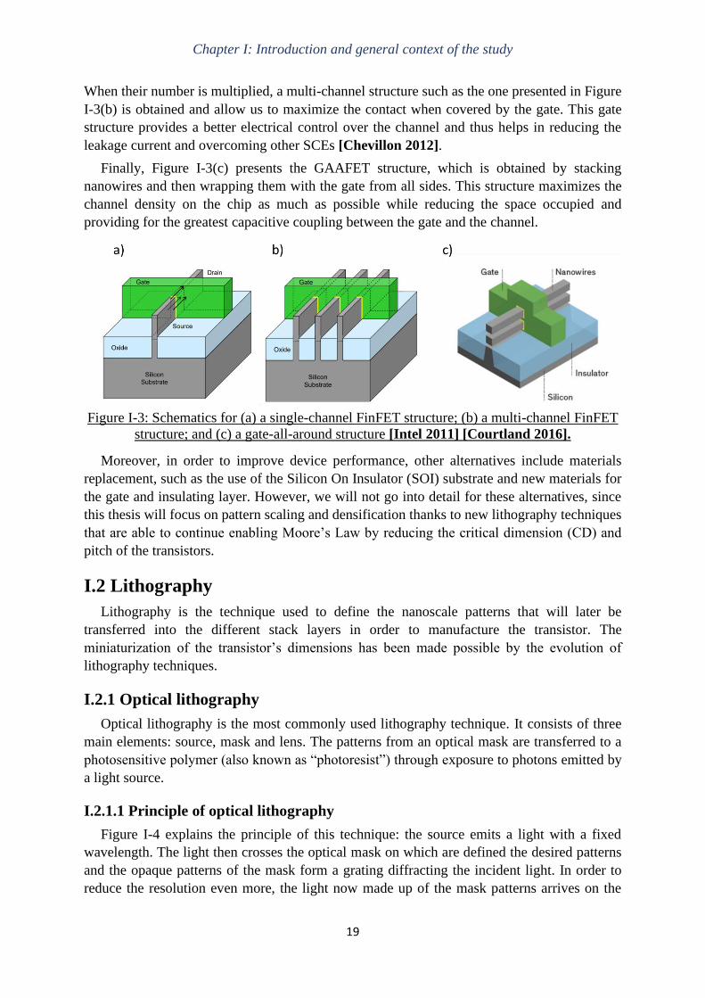
The FinFET (Fin Field-Effect Transistor) basic structure is presented in Figure I-3(a). The
main difference between the FinFET and the common MOSFET structure presented in Figure
I-2 is that the body of the FinFET device is formed by 3D conducting channels with a fin-like
structure. They are covered by the gate in order to increase their contact surface by 3D effect.
Chapter I: Introduction and general context of the study
19
When their number is multiplied, a multi-channel structure such as the one presented in Figure
I-3(b) is obtained and allow us to maximize the contact when covered by the gate. This gate
structure provides a better electrical control over the channel and thus helps in reducing the
leakage current and overcoming other SCEs [Chevillon 2012].
Finally, Figure I-3(c) presents the GAAFET structure, which is obtained by stacking
nanowires and then wrapping them with the gate from all sides. This structure maximizes the
channel density on the chip as much as possible while reducing the space occupied and
providing for the greatest capacitive coupling between the gate and the channel.
Figure I-3: Schematics for (a) a single-channel FinFET structure; (b) a multi-channel FinFET
structure; and (c) a gate-all-around structure [Intel 2011] [Courtland 2016].
Moreover, in order to improve device performance, other alternatives include materials
replacement, such as the use of the Silicon On Insulator (SOI) substrate and new materials for
the gate and insulating layer. However, we will not go into detail for these alternatives, since
this thesis will focus on pattern scaling and densification thanks to new lithography techniques
that are able to continue enabling Moore’s Law by reducing the critical dimension (CD) and
pitch of the transistors.
I.2 Lithography
Lithography is the technique used to define the nanoscale patterns that will later be
transferred into the different stack layers in order to manufacture the transistor. The
miniaturization of the transistor’s dimensions has been made possible by the evolution of
lithography techniques.
I.2.1 Optical lithography
Optical lithography is the most commonly used lithography technique. It consists of three
main elements: source, mask and lens. The patterns from an optical mask are transferred to a
photosensitive polymer (also known as “photoresist”) through exposure to photons emitted by
a light source.
I.2.1.1 Principle of optical lithography
Figure I-4 explains the principle of this technique: the source emits a light with a fixed
wavelength. The light then crosses the optical mask on which are defined the desired patterns
and the opaque patterns of the mask form a grating diffracting the incident light. In order to
reduce the resolution even more, the light now made up of the mask patterns arrives on the

Chapter I: Introduction and general context of the study
20
converging lens, which reduces the size of the patterns. Finally, the photoresist is exposed to
light in certain zones corresponding to the patterns of the mask with reduced sizes thanks to the
passage through the lens. Due to the light radiation received, a chemical reaction takes place
within the photoresist, inducing a difference in solubility between the exposed and unexposed
areas.
Two types of photoresists are used in microelectronics: positive and negative. If they are
exposed under the same conditions through the same mask, in the case of a positive photoresist,
the exposed part becomes soluble in the developer solution, while the non-exposed part remains
insoluble. In the case of a negative photoresist, it is the unexposed area which is soluble in the
developer. The patterns formed correspond to the non-soluble part. Both cases are represented
in the bottom of Figure I-4. Finally, the resultant photoresist pattern is used as an etch mask
during the pattern transfer steps in order to define small features on the wafer.
Figure I-4: Principle of optical lithography for positive and negative photoresists.
I.2.1.2 Evolution of optical lithography
As we have seen, optical lithography is a technique based on light diffraction, for which the
achievable resolution is determined by Rayleigh's law:
𝑅 = 𝑘 × 𝜆0𝑁𝐴
Equation I-1: Rayleigh’s law.
In which:
- 𝑅 is the resolution, which corresponds to the minimum achievable dimension or CD;
- 𝑘 is the Rayleigh coefficient of resolution, an empirical factor smaller than 1, which
depends on the optical devices, the photoresist and the type of mask used;
- 𝜆0 corresponds to the vacuum wavelength of the light source.

Chapter I: Introduction and general context of the study
21
- NA is the numerical aperture of the imaging system, with NA = n.sinɵ; where n is the
refractive index of the incident medium and ɵ is the angular aperture of the lens.
In order to increase the resolution and, consequently, decrease the size of the obtained
patterns, the different parameters present in Rayleigh’s law have been modified over the years.
The first parameter to be explored was the vacuum wavelength 𝜆0 of the light source, which
has been gradually decreased over the last 30 years, from 436 nm in the 1980s using a mercury
source to 193 nm since the 2000s using an argon fluoride (ArF) laser. The 193 nm ArF
lithography is currently used in manufacturing and is capable of obtaining patterns whose pitch
reaches minimum values of 160-180 nm, with CDs of 80-90 nm. Reducing the wavelength from
193 nm to 157 nm was abandoned, due to the rapid increase of technological challenges and
costs associated with developing new exposure tools and imaging materials [Sanders 2010].
Another parameter to be explored was the photoresist’s sensitivity to the light exposure.
Increasing this sensitivity made it possible to decrease the k parameter, thus maximizing the
resolution and the definition of the patterns. Chemically Amplified Resists (CARs) are an
example of innovation linked to this parameter.
Finally, the third parameter to be optimized was the numerical aperture (NA) of the imaging
system, which has been increased over the years in order to increase the resolution. Its angular
opening ɵ cannot be infinitely increased. Due to the geometry of the lens and the fact that light
travels in a straight line through homogeneous media, ɵ is limited to 90° and therefore sinɵ is
limited to 1.0. This leaves the refractive index n of the medium in which the lithography takes
place to be optimized. Traditionally, optical lithography is performed in air, which has a
refractive index of nair = 1.00. However, by changing to a medium with a higher refractive
index, such as water (nwater = 1.44), it is possible to further increase the resolution by reducing
the effective wavelength 𝜆𝑒𝑓𝑓:
𝜆𝑒𝑓𝑓 = 𝜆0
𝑛𝑚𝑒𝑑𝑖𝑢𝑚
Equation I-2: Effective wavelength.
From this equation, we can see that using water as an immersion fluid leads to a reduction
of around 30% in the effective wavelength of 193 nm lithography, which is more than would
be obtained by changing to 157 nm wavelength. This led to the creation of 193 nm immersion
lithography, which is capable of attaining CDs of around 40 nm and was introduced to industrial
manufacturing in 2005.
Another important advantage of 193 nm immersion lithography is that, since reducing 𝜆𝑒𝑓𝑓
does not change the frequency of the incident radiation, this technique is able to use much of
the already existing technology used in 193 nm dry lithography in terms of materials (mask,
lens, photoresist, and antireflective coating, for example) [Sanders 2010].
However, nowadays this method has reached its limits in terms of pattern scaling. With its
minimum CD of 30-40 nm for line/space applications, optical immersion lithography no longer
meets the expectations of manufacturers for technological nodes of 10 nm and beyond.
I.2.1.3 Multiple patterning: extending optical lithography limits
Among the techniques investigated to continue extending the optical lithography limits while
also retaining its equipment and methods for as long as possible, there is one known as Multiple

Chapter I: Introduction and general context of the study
22
Patterning Lithography (MPL), which consists of obtaining patterns through several steps. MPL
has been gradually developed over the last few years, until finally being used in production to
complement traditional optical immersion lithography.
The first example of a multiple patterning technique is the double patterning process, also
known as LELE (Litho-Etch-Litho-Etch), which is represented by the schematics in Figure I-
5(a). This technique consists of carrying out a first lithography, transferring the patterns into a
hardmask through etching, then carrying out a second lithography over the first one by shifting
the patterns by half a step in order to expose the new patterns in the middle of the previous ones,
and finally etching the hardmask using the newly-shifted patterns. For example, if we consider
that lines with 40 nm CD and 160 nm pitch are exposed and etched, each line is then 120 nm
apart. The second lithography is shifted by half a step compared to the previous one, i.e. 80 nm:
the new printed lines are located between the previous ones at a distance of 40 nm. A network
of lines of 40-nm CD which are 40 nm apart – obtaining a period of 80 nm – is then obtained,
making it possible to halve the lithography pitch. This means that, by shifting the second
exposure compared to the first, we are able to double the pattern density on our wafer. The
major advantage of this technique lies in the use of optical lithography and, therefore, it does
not require the development of new tools and materials.
However, when approaching the smaller nodes, even more Litho-Etch steps are necessary,
which not only significantly increases the cost but also highlights the main challenge of this
technique: the mask overlay problem, which is represented in Figure I-5(b). Indeed, the second
mask must be perfectly aligned with respect to the first level in order to avoid any overlapping
of patterns with respect to each other. The smaller the target dimensions, the more precise this
alignment must be [Levinson 2010]. For critical dimensions smaller than 20 nm, the cost and
overlay limitations are considered too critical for integration to be possible and, therefore, other
MPL approaches become more attractive.
Figure I-5: Schematic representation of the (a) LELE process and (b) the overlay problem.

Chapter I: Introduction and general context of the study
23
The most used MPL approach is the Self-Aligned Double Patterning (SADP), represented
in Figure I-6. In this approach, the first step consists of a standard 193 nm optical lithography
process to form patterns with a loose pitch. These patterns form the core material, known as
“mandrel”. The mandrel is then coated with a conformal thin film, known as “spacer”, which
is usually composed of silicon oxide (SiO2) or silicon nitride (SiN). Next, the spacer material
is anisotropically plasma etched in order to remove the thin film on the substrate and on the top
of the mandrel patterns, while leaving it intact on the sides. Afterwards, the mandrel is removed
by either plasma or wet etching, which must be very selective to both the spacer and the
substrate materials. At this stage, only the spacers remain and form a network of lines whose
pitch is equal to half the initial pitch and whose width is defined by the thickness of the spacer
deposited on the sides. Finally, we use the spacers created as a mask to transfer the patterns into
the subjacent layer.
With this technique, very uniform and resolved structures are thus obtained without the need
for multiple Litho-Etch type steps and, more importantly, by eliminating the need for alignment
methodology [Levinson 2010]. By repeating these steps, it is therefore possible to double,
quadruple (known as SAQP, for Self-Aligned Quadruple Patterning) and even octuplet (SAOP,
for Self-Aligned Octuplet Patterning) the density of 193 nm immersion lithography. Nowadays,
spacers offering guide widths up to 7 nm and obtaining dense line and space patterns with 5-
nm CDs have been demonstrated [Oyama 2014].
Figure I-6: Schematic representation of the SADP process using spacer patterning.
I.2.2 New lithography techniques to continue pattern scaling
As we have seen before, until around 2015 the ITRS determined which techniques had a
better chance of attaining the necessary pattern dimensions for the next technological nodes. In
2016, the ITRS was replaced by the IRDS (International Roadmap for Devices and Systems) in
order to address “a much broader approach to system integration, including, for example,
topics of communications spanning from conductors to wireless to fiber optics and exploring
non-electron-based technologies” [IRDS 2016]. Defined by the leading experts in
microelectronics, the IRDS is a roadmap to follow in order to allow the microelectronics
industry to evolve and meet economic criteria, becoming ever more competitive. It is updated
regularly and defines the next technological nodes, when they should be reached and also
through which means it should be made possible. The IRDS includes several different reports,
each one presenting a roadmap in terms of lithography techniques, transistor architecture,
number of metal levels, evolution of materials, and so on. Within the framework of this thesis,
we will focus on the IRDS recommendations for the evolution of the lithography techniques.
In this case, the IRDS proposes in particular to favor certain lithography techniques for the
various technological nodes according to their maturity.
Figure I-7 presents the lithography roadmap taken from the 2020 IRDS Lithography Report
[IRDS 2020]. It shows that optical immersion lithography no longer meets the demands of

Chapter I: Introduction and general context of the study
24
industry for the next technological nodes. Even though SAQP and SAOP using 193 nm
immersion lithography might be able to produce very small features, the complexity and the
rising costs of the associated processes make these techniques a short-term alternative while a
new, more resolving lithography technique makes the transition from lab to fab. This means
that, in order to continue pattern scaling, it is necessary to develop new lithography methods,
some of which are presented in Figure 1-7 either by themselves or associated with multiple
patterning techniques. The next sections will present some of these new techniques.
Figure I-7: The 2020 IRDS Lithography Report presented this roadmap for the line/space
potential solutions in lithography for the next 10 years. Adapted from [IRDS 2020].
I.2.2.1 Extreme Ultraviolet (EUV) lithography
Today the most developed and best placed solution to continue pattern scaling is the Extreme
Ultraviolet (EUV) lithography, as we can see in Figure I-7. This technology uses significantly
shorter wavelengths when compared to immersion lithography, which leads to better resolution.
The source used is a high-power laser striking a tin (Sn) droplet, forming a plasma emitting
radiation at a wavelength of 13.5 nm. In this range of extreme UV rays, also called soft X-rays,
the material strongly absorbs radiation. All the optical projection system based on focal lens
used by the 193 nm immersion lithography becomes therefore unusable for EUV. They are
replaced by a Molybdenum-Silicon (Mo-Si) multi-layer sheet mirror system which allows, by
multiple reflections, to conserve approximately 70% of the original signal. However, mirrors
present a low numerical aperture, introducing the need to use several of them in order to achieve
the desired resolution according to the Rayleigh criteria (equation I-1). There are four mirrors
used for the illuminator optics and six mirrors for the projection optics. Since the EUV mask in
itself counts as an additional mirror, there are at least eleven reflections, which means that only
around 2% of the EUV source light actually reaches the wafer [Mizoguchi 2017]. The
development of EUV sources powerful enough to compensate for these losses (and therefore
allow sufficient exposure doses) concentrates a large part of the development efforts for this
technology.
Chapter I: Introduction and general context of the study
25
Nowadays, Samsung and TSMC are the only companies that use EUV in production, mainly
targeting the 5 nm node [Samsung 2019] [Yeap 2019]. According to the IRDS 2020
Lithography roadmap, the implementation of EUV means that pattern scaling major challenges
for this technique are no longer resolution, but are instead related to Edge Placement Error
(EPE) effects, namely overlay, critical dimension uniformity (CDU) and line-edge roughness
(LER) [IRDS 2020]. IRDS also announces that some of the defects in EUV lithography are due
to random variations in light exposure and in resist chemistry, which are called stochastics.
Some examples of stochastics are bridging between lines, line breaks, missing contact holes or
merged contact holes. These stochastics defects only become more important as we reduce the
pitch of the desired features. Another challenge related to EUV lithography is the tool cost,
which can reach more than 100 million dollars per scanner [Shilov 2020]. Not all companies
can withstand its extremely high cost, hence the pursuit of research and development on other
techniques.
I.2.2.2 Nanoimprint lithography (NIL)
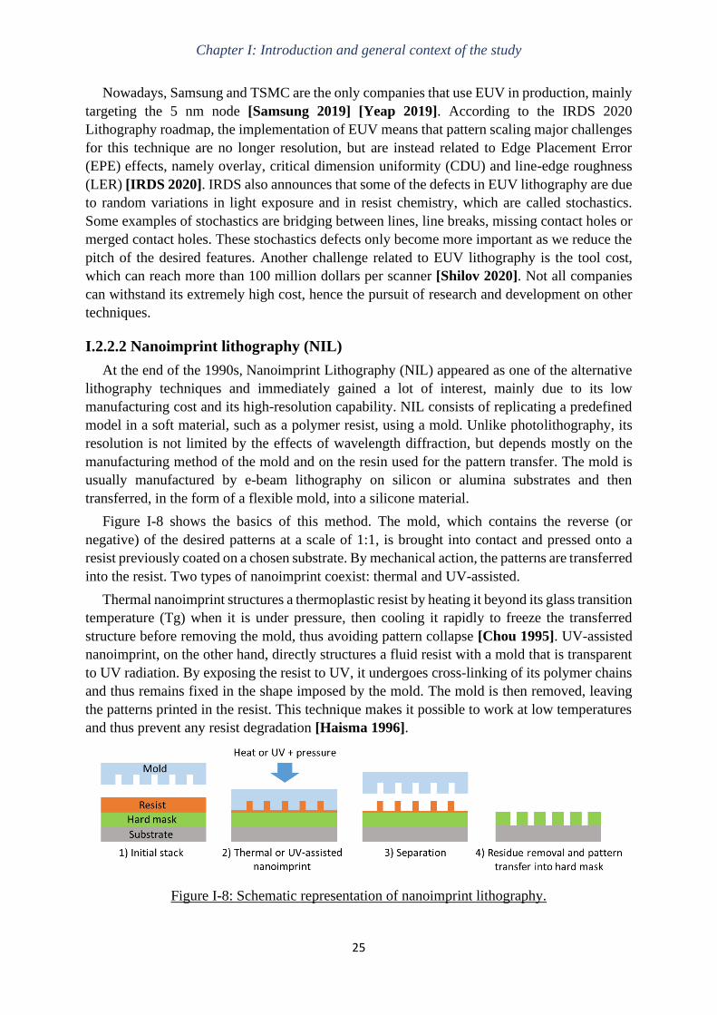
At the end of the 1990s, Nanoimprint Lithography (NIL) appeared as one of the alternative
lithography techniques and immediately gained a lot of interest, mainly due to its low
manufacturing cost and its high-resolution capability. NIL consists of replicating a predefined
model in a soft material, such as a polymer resist, using a mold. Unlike photolithography, its
resolution is not limited by the effects of wavelength diffraction, but depends mostly on the
manufacturing method of the mold and on the resin used for the pattern transfer. The mold is
usually manufactured by e-beam lithography on silicon or alumina substrates and then
transferred, in the form of a flexible mold, into a silicone material.
Figure I-8 shows the basics of this method. The mold, which contains the reverse (or
negative) of the desired patterns at a scale of 1:1, is brought into contact and pressed onto a
resist previously coated on a chosen substrate. By mechanical action, the patterns are transferred
into the resist. Two types of nanoimprint coexist: thermal and UV-assisted.
Thermal nanoimprint structures a thermoplastic resist by heating it beyond its glass transition
temperature (Tg) when it is under pressure, then cooling it rapidly to freeze the transferred
structure before removing the mold, thus avoiding pattern collapse [Chou 1995]. UV-assisted
nanoimprint, on the other hand, directly structures a fluid resist with a mold that is transparent
to UV radiation. By exposing the resist to UV, it undergoes cross-linking of its polymer chains
and thus remains fixed in the shape imposed by the mold. The mold is then removed, leaving
the patterns printed in the resist. This technique makes it possible to work at low temperatures
and thus prevent any resist degradation [Haisma 1996].
Figure I-8: Schematic representation of nanoimprint lithography.
Chapter I: Introduction and general context of the study
26
The production of lines with 5-nm width and 14-nm pitch has been demonstrated using UV-
assisted NIL [Austin 2004]. Nanoimprint patterning tools are considerably cheaper than high-
performance optical lithography exposure tools because there is no high-resolution lens
required. However, due to the mechanical nature of NIL, its tools present significantly less
throughput than typical of optical lithography systems. Another advantage of this method is
that the challenge of obtaining high resolution critical dimensions is carried over to the initial
production of the mold alone. Even if the mold is complex and long to create, each
nanoimpression made from it is then no more than a simple faithful reproduction.
However, for the future technological nodes with sub-20nm resolutions, since the mold
presents a scale of 1:1, they become difficult to make for logic and DRAM leading edge feature
sizes. The fabrication cost of the initial mold becomes not negligible, and the resist indentation
mechanics become more complex at this nanometric scale, in particular because of the greater
mold adhesion phenomena. Finally, the levels of defectivity achieved by this technique are still
below the expectations of the logic industry. NIL is, therefore, used in applications which are
defect tolerant [Takeishi 2015].
The IRDS Lithography report for 2020 announces that, since 3D flash memory has much
larger feature sizes than 2D flash, manufacturing grade tools are in use for pilot production for
this application, with high-volume manufacturing being possible in 2021 [IRDS 2020].
I.2.2.3 Electron-beam lithography
Electron-beam (or “e-beam”) lithography (EBL) is able to create patterns on wafers directly,
without the use of a mask. Electrons have noticeably short wavelengths at the energies typically
used for EBL (5–100 keV). Therefore, this technique has potential for extremely high
resolution, producing features 10 nm and smaller [Craighead 1984].
In the same way as photolithography, the e-beam irradiates a resist sensitive to this energy
range, which will modify its solubility in the development solvent used: either by becoming
more soluble (positive EBL) or by cross-linking, rendering it less soluble (negative EBL). The
application of its solvent will then selectively remove (for positive EBL) or leave (for negative
EBL) the exposed areas on the surface. The limit of resolution is therefore more dependent on
the chemical sensitivity of the resist to the electron than on the size of the beam itself.
Nevertheless, it has drawbacks, such as the emission of backscattered electrons at a short
distance by the very energetic beams, which are capable in turn of modifying the resist and
therefore enlarging the printed pattern.
Unlike photolithography, which simultaneously insolates the entire surface of wafer, EBL
produces continuous writing, pattern by pattern. Therefore, it has great flexibility in its drawing
rules, but on the other hand, its yield is extremely low and incompatible with high-volume
manufacturing. This is why its use is currently limited to mask manufacturing, low volume
production and R&D.
In order to achieve throughputs superior to 10 wafers per hour, an alternative method known
as Massively Parallel-Electron Beam Direct Write (or “multi-beam”) has been proposed by
some companies. Based on the same principle as the e-beam, it combines several electron beams
in parallel, each working on nearby areas to decrease writing time [Pourteau 2016]. For
example, MAPPER systems with tens of thousands of beams have been proposed. However,
increased number of beans means increased currents, which will then heat the wafers, and the

Chapter I: Introduction and general context of the study
27
resulting thermal expansion will cause overlay errors. Even with beam energies as low as 5
keV, such as proposed by MAPPER, overlay errors greater than 2 nm can result from EBL–
induced heating. These overlay errors become too important for sub-20 nm nodes and, along
with low throughput, have removed EBL from the list of possible lithography approaches to
continue pattern scaling in high-volume manufacturing [Levinson 2010].
I.2.2.4 Directed Self-Assembly (DSA) of block copolymers
The previous methods presented follow the "top-down" principle, in which the
morphological and dimensional information of nanoscale patterns are created by larger,
externally controlled sources such as photons or electrons. The technique that has been studied
in the framework of this thesis, however, follows a "bottom-up" strategy, which assembles
atoms and molecules in structures of shape and dimensions determined by the physical-
chemical nature of the material used: the Directed Self-assembly (DSA) of block copolymers
(BCPs). The next section will go into detail of this technique, showing its potential to
complement and improve the performance of already existing lithography methods, such as
immersion photolithography, multiple patterning and EUV lithography.
I.3 Directed Self-Assembly of Block Copolymers
DSA is one of the low-cost solutions proposed by the IRDS to obtain small and dense
patterns for the sub-10 nm nodes. This technique is based on the self-assembling property of
block copolymers, which are able to microphase separate, spontaneously forming a dense array
of different ordered nanostructures, like cylinders or lamellae, with domain dimensions of
around 5 to 50 nm [Lane 2017] [Isono 2018].
The idea of using these structures in microelectronics was first introduced in 1996 by P.
Mansky et al. [Mansky 1996]. Since then, research activity on block copolymers made a real
leap forward. This approach has many promising points: the cost of polymer materials is low
compared to lithography industry standards; the process is relatively simple and fast since it
consists of coating and annealing polymeric materials; and the resolution and density achieved
are equal to or greater than that of the other alternatives presented so far.
I.3.1 Block copolymers definition
A copolymer is a polymer derived from more than one species of monomer. There are
different types of linear copolymers, depending on the way that the monomers polymerize:
- Alternating copolymers: the monomers are regularly alternating, like A-B-A-B-A-B-A-B
- Random copolymers: the monomers are arranged in any order, like A-A-B-A-B-B-A-B
- Block copolymers: composed of two or more homopolymers linked by covalent bonds, like
A-A-A-A-B-B-B-B.
In this thesis, we will focus on diblock copolymers since they are the ones that present an
interest for the microelectronics industry due to their ability to self-assemble at the nanoscale.
Moreover, the structures formed are inherently periodic, uniform and reproducible.
If the two blocks have different solubility parameters, they tend to minimize their free energy
(and therefore their contact surface) by repelling each other, which induces a separation
between them. The advantage of using block copolymers, instead of a mixture of two

Chapter I: Introduction and general context of the study
28
homopolymers, lies in the covalent bond which binds them to each other. Because of this bond,
the phase separation takes place only on a scale similar in size to that of the copolymer, meaning
the nanoscale [Morris 2015]. The micro domains obtained have a size which can range from 5
to 100 nm depending on the properties of the polymers constituting it [Stoykovich 2006].
The Flory-Huggins interaction parameter, also known as “chi” or χ, represents the strength
of repulsive interaction between two blocks. This parameter is defined by Equation I-3 for the
copolymer blocks A and B. εXY represents the interaction energy per monomer between X and
Y monomers, kB represents the Boltzmann constant, T represents the temperature and Z
represents the coordination number, that is, the number of nearest neighbor monomers for a
lattice site:
𝜒𝐴𝐵 =𝑍
𝑘𝐵𝑇 [𝜀𝐴𝐵 −
1
2(𝜀𝐴𝐴 + 𝜀𝐵𝐵)]
Equation I-3: Flory-Huggins interaction parameter χ for two copolymer blocks A and B
[Bates 1999].
A positive value of the Flory-Huggins parameter χ corresponds to a net repulsion between
the two blocks present, generally causing phase separation, while a negative value indicates a
free-energy drive towards mixing. As we can see from Equation I-3, the Flory-Huggins
interaction parameter is inversely proportional to the temperature, which means that the more
the temperature increases, the lower χ will be, favoring mixing.
When the χ between the two blocks is positive, obtaining microphase structures with a block
copolymer is possible depending on the degree of polymerization (N) of the block copolymer
and on process temperature. The strength of the repulsive interaction is characterized by the
product χN. A product χN = 10.5 has been calculated as the location of the order-disorder
transition (ODT). Thus, diblock copolymers of high molecular weight or with strongly
incompatible blocks (χN > 10.5) are predicted to be microphase separated, whereas smaller
copolymers with more compatible blocks (χN < 10.5) are predicted to show no microphase
separation [Bates 1999].
The morphology of the structures formed after microphase separation depend on the volume
fraction (f) of each phase and on the product χN. Figure I-9 shows the typical phase diagram
for a diblock copolymer as well as the different morphologies that might be obtained depending
on the volume fraction of each phase. We note that the parameter χN has little influence on the
morphology except when χN < 10.5 (represented as DIS in the phase diagram), because in this
case the phases do not segregate and therefore no pattern is formed. For χN > 10.5, the volume
fraction of each phase determines the corresponding structure: lamellar (LAM) when fA = fB =
0.5, followed by gyroidal (GYR), cylindrical in hexagonal (HEX) structure and spherical in
body-centered cubic (BCC) structure, respectively, as the volume fraction of one of the blocks
increases. A rarer cubic close-packed structure (CPS) is also possible [Cochran 2006] [Kim
2010].
Amongst these structures, two have been investigated the most for microelectronic
applications: cylinders and lamellae structures. Once one phase has been selectively removed
from the other in order to obtain an etch mask, cylinders allow for contact hole patterning while
lamellae are used for line/space patterning [Kim 2010].

Chapter I: Introduction and general context of the study
29
Figure I-9: On the left, a typical phase diagram for a diblock copolymer adapted from
[Cochran 2006]. On the right, the possible morphologies for the diblock copolymer
depending on the volume fraction (f) of the red phase [Koo 2013].
The Flory Huggins interaction parameter χ also has a very important role in the definition of
the block copolymer’s intrinsic period (L0), which corresponds to a repeating unit of the block
copolymer (one A block and one B block) and is equivalent to the pitch of the nanostructures
obtained. The period of the block copolymer is a key parameter for the semiconductor industry,
since it determines the size of the patterns obtained.
In order to determine L0, different proportionality laws have been established over the years
by research groups [Sivaniah 2008] [Matsushita 1990]. All of them agree on the
proportionality between the period and the degree of polymerization of the polymer:
𝐿0 ∝ 𝑁𝛼
Equation I-4: Proportionality law for determining the intrinsic period L0 of the block
copolymer.
The exponent α varies depending on the degree of phase separation. The phase diagram
presented in Figure I-9 can be divided into three horizontal segments defining segregation zones
characteristic of three different values of the product χN:
- Strong Segregation Limit (SSL): this segment is not represented on the phase diagram, but
corresponds to the product χN >> 100. In this zone, the coefficient α has been demonstrated to
be 2/3 [Hashimoto 1980]. For the SSL, a more precise law of proportionality also involves the
Flory-Huggins parameter χ, with a representing the statistical length of the monomer:
𝐿0~ 𝑎𝜒16𝑁
23
Equation I-5: Proportionality law for the intrinsic period L0 of the block copolymer in the
strong segregation limit.
- Weak Segregation Limit (WSL): this segment is located in the lower part of the phase
diagram, where the product χN < 40. In this segment, the coefficient α is close to 1/2.
- Intermediate Segregation Regime (ISR): this segment constitutes the heart of the diagram,
where 40 < χN <100. In this zone, the value of α varies between 0.72 and 1.017 (theoretical) or
0.80 and 0.83 (experimental) [Sivaniah 2008].

Chapter I: Introduction and general context of the study
30
In order to have stable structures which are better suited to the lithography requirements, it
is preferable to be in the regime of strong segregation (SSL). In the SSL, the well-defined
interface width leads to lower pattern roughness. Moreover, the fact that the transitions between
morphologies are independent of χ and of N ensures better reproducibility of the results. Finally,
since Equation I-5 establishes that the period L0 is defined by intrinsic parameters of the
material, full control over all dimensions of the nanostructures is possible.
The most commonly studied block copolymer for the DSA application is the polystyrene-b-
poly(methyl methacrylate), also known as PS-b-PMMA, due to its easy synthesis and well-
known properties [Argoud 2014]. However, PS-b-PMMA presents a relatively low Flory-
Huggins parameter (χ ≈ 0.06 at 298K [Girardot 2014]). In order to satisfy the condition for the
order-disorder transition (χN > 10.5), the minimum pitch for the PS-b-PMMA system is limited
to around 24 nm for minimum degrees of polymerization N ≈ 500.
Therefore, in order to obtain resolutions lower than that of PS-b-PMMA and remain
attractive for the smaller technological nodes, the most common strategy consists in increasing
the value of χ. Doing so allows us to reduce the value of N – and thus also reduce the BCP’s
period – without violating the condition of the order-disorder transition. This “strong χ / weak
N” approach has given rise to the development of so-called “high-χ” block copolymer systems
over the past years [Feng 2017]. Moreover, the increase in χ leads to an increase in repulsion
between the blocks: the domains are thus better defined and present better Line-Edge
Roughness (LER) and Line-Width Roughness (LWR) compared to PS-b-PMMA [Tsai 2016].
The high-χ BCP systems currently under investigation can be divided into two main groups:
organic and inorganic high-χ block copolymers.
Purely organic high-χ block copolymers are developed based on monomers of very different
polarity (such as PS-b-P2VP with χ ≈ 0.18 [Gu 2012]) or hydrophobicity (PCHE-b-PMMA
[Kennemur 2014] with χ ≈ 0.32 and capable of producing sub-8 nm lamellae). Using highly
hydrophobic blocks like polylactic acid in a PS-b-PLA also increases incompatibility and
results in χ ≈ 0.23 [Zalusky 2002]. Another example of purely organic high-χ BCPs includes
the “HC series” developed by EMD Performance Materials with pitch of 17 to 26 nm
[Hirahara 2016]. Other authors have started from the structure of PS-b-PMMA by adding a
third monomer. This is the case, for example, of Zhou et al. who introduce vinylnaphthalene
into the chain of the PS block to form a poly((styrene-random-vinylnaphthalene)-block-methyl
methacrylate) (PSVN-b-PMMA) BCP and double the χ parameter of PS-b-PMMA [Zhou
2016].
Inorganic high-χ block copolymers usually consists of one organic phase (for example, PS
or PMMA) covalently bound to one phase containing an inorganic element, such as silicon or
iron. The use of inorganic blocks makes it possible to increase the χ parameter while also
significantly increasing the etching contrast. Most of the inorganic high-χ BCPs present a
silicon-containing phase such as polydimethylsiloxane (PDMS) as one of the blocks.
Poly(styrene-block-dimethylsiloxane) (PS-b-PDMS) (χ = 0.26 at 300K and pitch of 14 nm)
[Girardot 2014] and poly(lactic acid-block-dimethylsiloxane (PLA-b-PDMS) (χ = 1.41 at
300K) are some of the examples found in the literature. K. Aissou et al. demonstrated a
templated semicrystalline poly(1,1-dimethylsilacyclobutane-block-methyl methacrylate)
(PDMSB-b-PMMA) thin film enabling the production of highly ordered cylinders of 9-nm
diameter [Aissou 2015]. Luo et al. studied a PDMS-b-PMMA with χ = 0.24 at 300K,
demonstrating well-ordered sub-10 nm line and sphere features under either thermal or solvent

Chapter I: Introduction and general context of the study
31
annealing conditions [Luo 2015]. Durand et al. demonstrated a poly(4-methoxystyrene-block-
4-trimethylsilylstyrene) (PMOST-b-PTMSS) with 20-nm and 14-nm pitch [Durand 2015].
Finally, Rodwogin et al. reported on the assembly of a PLA-b-PDMS-b-PLA triblock
copolymer which presents a χ = 1.4 at 298K and is able to form lamellar, cylindrical and
spherical morphologies with sub-20 nm pitch [Rodwogin 2010]. Iron-based block copolymers
such as poly(nonafluorohexyl methacrylate-block-ferrocenylmethyl methacrylate) (PF9MA-b-
PFMMA) have also been demonstrated [Chernyy 2017].
Organic and inorganic high-χ block copolymers present both advantages and limitations
when it comes to their application in lithography. Organic block copolymers usually present an
easier synthesis, while inorganic BCPs most of the times demand additional processing, such
as solvent annealing, addition of a top coat, and others. Inorganic BCPs are considered better
options for etching, since it is easier to obtain a good etching selectivity between inorganic and
organic phases. However, a higher incompatibility between the two blocks also presents some
drawbacks: these BCPs usually have a high diffusive energy barrier and slow kinetics as well
as a preferential wetting of one of the blocks to the air interface [Mokarian-Tabari 2014].
Organic BCPs, on the other hand, are known for having lower etching selectivity between the
two organic phases which, combined with the smaller dimensions (thickness and pitch), renders
the pattern transfer into the subjacent layers more challenging. Furthermore, other advantages
and challenges related to each type of high-χ BCP will be presented in the next section, when
we explain the procedure for obtaining a BCP film.
I.3.2 Obtaining a block copolymer thin film
The block copolymers are often supplied in solution, which is then deposited by spin-coating
on the wafers. The speed of rotation of the spinner as well as the viscosity and concentration of
the solution determine the thickness of the copolymer film obtained.
As deposited in a thin film on a wafer, block copolymers are in a disordered state, where the
domains between each block are not defined. The different film deposition parameters (speed
of rotation, evaporation of the solvent, etc.) can slightly influence the shape of the polymer
chains on the wafer. However, the domains are not defined at this stage due to the low self-
assembly kinetics of the chains. Micro-phase separation is above all a thermodynamic
phenomenon, requiring an input of energy into the system to separate the different phases. The
most widely used method is thermal annealing. The wafer is placed in an oven heated to a
temperature above both the glass transition temperature (Tg) and the order-disorder temperature
(TODT) of the two blocks and below their degradation temperature. The kinetics of the micro-
phase separation are increased due to the increased mobility of the chains and, therefore, the
domains between the blocks are formed. The ideal annealing time and temperature are different
depending on the thickness and the morphology of the film, but also the length of the copolymer
chains [Choi 2010] [Tseng 2010].
Obtaining microphase separation and forming the desired nanostructure (lamellae or
cylinders, for example), however, is often not enough to use these block copolymers in
lithography. The two blocks should be oriented on the substrate in such a way that the patterns
defined by it can be transferred through etching to the substrate or to the underlying materials.
Therefore, they must have a perpendicular orientation, meaning that the two blocks of the
copolymer must be in contact with the surface of the substrate. Indeed, in order to incorporate
the DSA into the microelectronics industry, one of the most important aspects is controlling the
Chapter I: Introduction and general context of the study
32
block copolymer’s orientation. Such orientation is defined by surface properties, particularly
the affinity between the two blocks and the surfaces they are in contact with, like the substrate
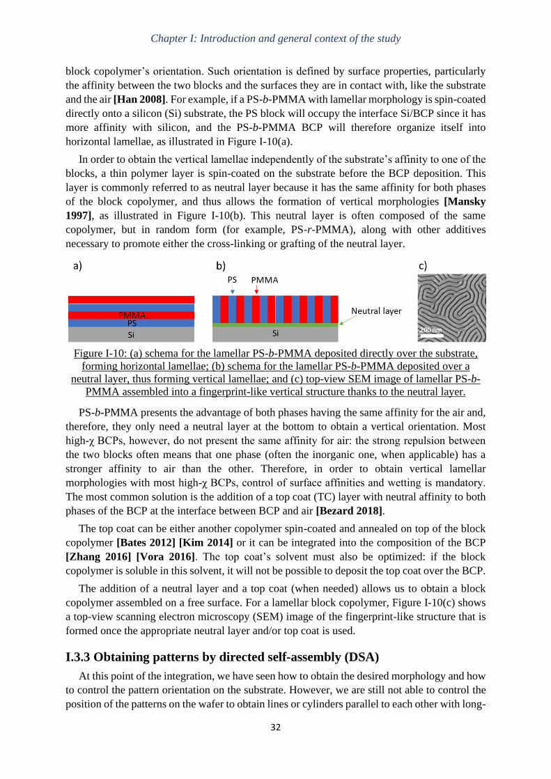
and the air [Han 2008]. For example, if a PS-b-PMMA with lamellar morphology is spin-coated
directly onto a silicon (Si) substrate, the PS block will occupy the interface Si/BCP since it has
more affinity with silicon, and the PS-b-PMMA BCP will therefore organize itself into
horizontal lamellae, as illustrated in Figure I-10(a).
In order to obtain the vertical lamellae independently of the substrate’s affinity to one of the
blocks, a thin polymer layer is spin-coated on the substrate before the BCP deposition. This
layer is commonly referred to as neutral layer because it has the same affinity for both phases
of the block copolymer, and thus allows the formation of vertical morphologies [Mansky
1997], as illustrated in Figure I-10(b). This neutral layer is often composed of the same
copolymer, but in random form (for example, PS-r-PMMA), along with other additives
necessary to promote either the cross-linking or grafting of the neutral layer.
Figure I-10: (a) schema for the lamellar PS-b-PMMA deposited directly over the substrate,
forming horizontal lamellae; (b) schema for the lamellar PS-b-PMMA deposited over a
neutral layer, thus forming vertical lamellae; and (c) top-view SEM image of lamellar PS-b-
PMMA assembled into a fingerprint-like vertical structure thanks to the neutral layer.
PS-b-PMMA presents the advantage of both phases having the same affinity for the air and,
therefore, they only need a neutral layer at the bottom to obtain a vertical orientation. Most
high-χ BCPs, however, do not present the same affinity for air: the strong repulsion between
the two blocks often means that one phase (often the inorganic one, when applicable) has a
stronger affinity to air than the other. Therefore, in order to obtain vertical lamellar
morphologies with most high-χ BCPs, control of surface affinities and wetting is mandatory.
The most common solution is the addition of a top coat (TC) layer with neutral affinity to both
phases of the BCP at the interface between BCP and air [Bezard 2018].
The top coat can be either another copolymer spin-coated and annealed on top of the block
copolymer [Bates 2012] [Kim 2014] or it can be integrated into the composition of the BCP
[Zhang 2016] [Vora 2016]. The top coat’s solvent must also be optimized: if the block
copolymer is soluble in this solvent, it will not be possible to deposit the top coat over the BCP.
The addition of a neutral layer and a top coat (when needed) allows us to obtain a block
copolymer assembled on a free surface. For a lamellar block copolymer, Figure I-10(c) shows
a top-view scanning electron microscopy (SEM) image of the fingerprint-like structure that is
formed once the appropriate neutral layer and/or top coat is used.
I.3.3 Obtaining patterns by directed self-assembly (DSA)
At this point of the integration, we have seen how to obtain the desired morphology and how
to control the pattern orientation on the substrate. However, we are still not able to control the
position of the patterns on the wafer to obtain lines or cylinders parallel to each other with long-

Chapter I: Introduction and general context of the study
33
range order. Obtaining a three-dimensional control of the two phases requires a new constraint
to be imposed on the block copolymer. The ensemble of guiding methods is referred to as
Directed Self-Assembly, or DSA, and differ in the way they enforce the orientation control.
Their common philosophy is to use the perfect alignment of well-established conventional
lithography (top-down approach) so that the phase microseparation of the block copolymer
(bottom-up approach) reproduces it at smaller resolution and higher density.
Two main approaches have been developed over the years: chemo-epitaxy and grapho-
epitaxy. In both cases, the block copolymer is constrained in order to organize itself and form
the desired line/space or contact holes pattern. The grapho-epitaxy is mainly based on
mechanical constraints while the chemo-epitaxy is mainly based on chemical affinity
constraints [Ji 2016].
I.3.3.1 Grapho-epitaxy
Segalman et al. first demonstrated the grapho-epitaxy technique back in 2001, using sphere-
forming PS-b-P2VP block copolymers [Segalman 2001]. This guiding method uses mechanical
constraints, such as topographical features obtained by conventional lithography, to act as
guide-patterns for the block copolymer’s self-assembly. The BCP is coated and annealed in the
space between the guides. For lamellar BCPs, the sidewalls of the guide-patterns preferentially
attract one domain of the BCP, allowing lamellar line/space patterns to form parallel to the
sidewalls of the guide, as we can see in Figure I-11.
Figure I-11: Principle of grapho-epitaxy guiding method: (a) topographical features obtained
by conventional lithography, which act as guide-patterns for the block copolymer’s self-
assembly (b) without or (c) with neutral layer, leading to the results observed in (d) the top-
view SEM image of a lamellar PS-b-PMMA aligned using grapho-epitaxy [Claveau 2016].
The commensurability between the width of the trench guide structure (W) and the period
L0 of the block copolymer used must be respected for the good organization of the BCP within
the guide. Different studies have shown that good organization is obtained when this width is
proportional to the period of the block copolymer (W = n * L0), which favors the formation of
an exact number of n domains. Conversely, approaching W = (n + 0.5) * L0, a coexistence
between two favorable states (n and n + 1) is preferred [Claveau 2016] [Cheng 2004].

Chapter I: Introduction and general context of the study
34
Therefore, the trench guide width is equally chosen according to the multiplication factor (n)
that we want to achieve. For a lamellar BCP, this factor qualifies the number of lamellae
obtained (by one of the two polymers) within a guide.
The height of the trench guide structure (h) is also a parameter to be taken into account
during grapho-epitaxy. For the topography confinement effect to prevail over the other
interfaces, h must be at least equal to the intrinsic period L0 of the BCP used. Several works
have shown that the ratio between the thickness of the deposited copolymer (t) and the trench
height (h) plays a determining role in the orientation and the level of defects of the final
assembly [Yang 2009]. The results of Park et al. show that for a lamellar PS-b-PMMA, when
the t/h ratio > 1, the material present above the trenches is no longer confined and adopts a
fingerprint structure [Park 2009].
Despite the stress applied to the block copolymer by the topological guide, it is also
necessary to control the affinity of the copolymer with the walls and the bottom of the trenches
[Koo 2013]. Indeed, Figure I-11(b) shows that, for line/space applications using a PS-b-PMMA
lamellar block copolymer aligned by grapho-epitaxy, a wetting layer composed of the block
that has the most affinity for the substrate is formed on the interface between the BCP film and
the substrate, which renders pattern transfer more difficult [Claveau 2017]. Therefore, a neutral
layer may be deposited only at the bottom of the trenches to eliminate the wetting layer, as
shown in Figure I-11(c). Several solutions to obtain different affinities at the walls and the
bottom of the trenches have been developed by CEA Leti through the use of a sacrificial layer
[Delachat 2018] or UV exposition [Pimenta-Barros 2018], and also by Imec through
preferential grafting of two different polymeric layers [Doise 2017].
IBM, CEA-Leti and others have demonstrated different grapho-epitaxy approaches applied
to an integration. There are two main types of applications for which grapho-epitaxy has been
demonstrated: contact hole shrink for vertical connections and line multiplication for
interconnections, gates and active areas of transistors [Cheng 2010] [Black 2005].
For line/space applications, IBM reported on the first DSA-patterned FinFET fabricated
using the tone-inverted grapho-epitaxy resolution enhancement (TIGeR) technique with a 29-
nm pitch PS-b-PMMA. A schematic representation of the TiGeR process can be found in Figure
I-12. The BCP is oriented by SiOx guiding patterns formed by e-beam lithography of hydrogen
silsesquioxane (HSQ) resist, which converts the HSQ into a low quality SiOx. After forming
the DSA patterns, the PMMA domains are selectively removed from the BCP, except for the
PMMA half-domains formed between the PS and the SiOx guide. The lines pattern is then
transferred into the silicon nitride (SiN) hard mask and the organic planarizing layer (OPL). A
tone-inversion process is then applied in the OPL layer by spin-coating a spin-on dielectric
material, etching back to reveal the OPL, followed by removal of the OPL. Finally, the tone
inverted image is transferred into a thin SiN hard mask layer and into the silicon on insulator
(SOI) underneath [Tsai 2014].

Chapter I: Introduction and general context of the study
35
Figure I-12: Schematics for the tone-inverted grapho-epitaxy resolution enhancement
(TIGeR) technique used by IBM to obtain 29-nm pitch DSA-patterned FinFETs [Tsai 2014].
Grapho-epitaxy has also been used in contact shrink applications, making it possible to
obtain contacts with dimensions not attainable by conventional lithography (around 20 nm) and
with very good alignment. Chang et al. have shown that the use of block copolymers organized
by grapho-epitaxy can meet the requirements in terms of electrical results for obtaining devices
for sub-20 nm technological nodes. They have demonstrated top gated FETs and CMOS
inverters featuring 20-nm contact holes defined by PS-b-PMMA using guide trenches with a
width of 60 nm obtained by optical lithography in order to obtain a row of contacts of 20 nm
with the BCP [Chang 2009] [Wong 2012].
Through these examples, we can see the different possibilities available for microelectronics
thanks to the organization of block copolymers by grapho-epitaxy. Nevertheless, this technique
presents some limitations. Since the topographical features occupy some space on the wafer
surface, grapho-epitaxy presents a lower pattern density when compared to the other DSA
approach (chemo-epitaxy). In addition, all defects of the guiding topographical prepattern (for
example, the line-edge roughness of its sidewalls) may propagate into the adjacent self-
assembled domains and cause additional CD variation and placement error [Cheng 2010].
While the use of grapho-epitaxy for contact hole shrink is validated, when it comes to
obtaining line/space patterns, chemo-epitaxy is often preferred.
I.3.3.2 Chemo-epitaxy
Chemo-epitaxy consists of a guiding method by surface property change of the substrate that
is to receive the block copolymer. Overall, the principle of chemo-epitaxy is based on the long-
range alignment of a block copolymer thanks to the presence of narrow guiding stripes that
present a chemical affinity to one of the blocks. These guiding stripes present a CD
corresponding to half the period of the block copolymer (L0) and are interlaced with wide
neutral layer stripes on the substrate surface. If the distance between each guide follows the
commensurability rules, when the BCP is coated and annealed over the surface, the guiding
stripes will attract one of the blocks and induce the BCP to organize itself in the desired patterns
(usually line/space) over long distances. For this, the distance between each guide (W) must be
proportional to the BCP’s period: W = n * L0, where n is once again the multiplication factor
(MF) [Hu 2014].

Chapter I: Introduction and general context of the study
36
Different chemo-epitaxy processes have been developed over the last few years, like LiNe
[Liu 2011], Lift-off [Cheng 2010], and SMART [Kim 2013], amongst others. With the current
chemo-epitaxy methods, it is possible to achieve multiplication factors of two or three, and
sometimes even four. Beyond this, the higher multiplication factors generate high defectivity,
which no longer allows the block copolymer to be integrated in a manufacturing process.
The LiNe integration, named after the two inventors Liu and Nealey, is the most popular
one. Figure I-13 presents the principles of this technique. To direct the self-assembly of PS-b-
PMMA, for example, a cross-linkable polystyrene (X-PS) layer is deposited over silicon. This
layer is identified as “mat” in Figure I-13. Then 193nm immersion lithography, consisting of
deposition of the photoresist and definition of the patterns, is carried out so that the pitch of the
patterns created is an integer number of times greater than the period of the copolymer (L0).
The resulting structures are treated with an oxygen-based plasma trim etch that laterally shrinks
the photoresist lines and removes X-PS in the spaces between them. When the line/space
patterns transferred to the X-PS have been reduced to a CDguide of approximately 0.5 * L0, the
remaining photoresist is stripped. Next, a PS-r-PMMA designed to be non-preferential to the
two blocks, identified as “brush” in Figure I-13, is grafted between the remaining XPS
structures. This results in a two-tone pattern of sparse X-PS guide stripes and background brush
regions. Finally, the block copolymer is deposited and, because of the chemical affinity, the X-
PS structures attract the PS block. Annealing then allows the block copolymer to organize itself
[Liu 2013]. This flow has been generalized for use with many different BCP systems by
changing the guiding mat and background materials [Bates 2014] [Khaira 2014].
Figure I-13: Schematics for the LiNe chemo-epitaxy integration. Adapted from [Liu 2013].
A few years later, studies by Williamson et al. demonstrated the critical importance of
oxidized X-PS sidewalls during oxygen plasma breakthrough and trimming for the success of
the LiNe integration. These highly hydrophilic areas, which are PMMA-attractive, create
additional chemical contrast and contribute just as much for self-assembly guiding as intact X-
PS. Unlike the IBM or AZ methods, LiNe chemo-epitaxy is therefore generated by a constraint
of not only two but rather three tone zones (PS-attractive, PMMA-attractive and neutral)
[Williamson 2016]. This three-tone chemical contrast could explain why the defectivity of
LiNe is much better than that of the other two processes [Somervell 2012].
IBM developed an integration called “Lift-off”, shown in Figure I-14, which consists of a
pattern-first, neutralize-last process to fabricate chemical prepatterns. First, polarity-switched
Chapter I: Introduction and general context of the study
37
photoresist prepatterns consisting of around 30-nm lines and 100-nm pitch are formed using
193 nm immersion lithography. These prepatterns mask some areas of the substrate while a
neutral layer is grafted over the whole surface. Subsequent selective lift-off of the photoresist
using standard TMAH developer generates sparse chemical patterns suitable for DSA. Finally,
the block copolymer is spin-coated and annealed in order to obtain straight lines. This
integration allows for a more relaxed resist lithography at CDguide = 2 * L0 or 3 * L0. Also, since
the neutral layer is applied last in this process, the photoresist pattern can be trimmed to
overcome the restrictions of the optical lithography tool without any damage to the surface
properties of the underlayers [Cheng 2010]. This process has been shown to be fully compatible
with industry 300 mm tools on the Imec pilot line [Somervell 2012].
Figure I-14: Schematics for the Lift-off chemo-epitaxy integration developed by IBM
[Somervell 2012].
AZ's SMART™ (Surface Modification for Advanced Resolution Technology) integration is
presented in Figure I-15. It follows the same relaxed lithography principle as IBM except that
it starts with a cross-linkable PS-r-PMMA neutral layer, identified as NLD-175, deposited over
the substrate. Then the photoresist is spin-coated on top of the neutral layer and 193 nm
immersion lithography is carried out to obtain the resist prepatterns. An oxygen-based Reactive
Ion Etching (RIE) is performed to remove the neutral layer at the bottom of the resist trenches.
The remaining resist is then stripped and a substrate alternating PS-r-PMMA neutral layer and
vacant areas is obtained. In some cases, this chemical contrast is enough to align the BCP.
However, for a more stable performance, a thin layer with affinity to one of the blocks
(identified as NLD-226) is spin-coated and grafted. This layer presents high reactivity to the
substrate (SiARC in this case) and low reactivity to the neutral layer (NLD-175), ensuring that
the NLD-226 that is deposited over the NLD-175 does not graft to it and is therefore removed
during rinse. This way, only a monolayer of NLD-226 is left in the trenches, increasing the
chemical contrast and leading to the alignment of the block copolymer [Kim 2013]. A step of
a few nanometers is present at the interface between NLD-175 and NLD-226: due to the
introduction of topography, the stresses brought to the copolymer are greater and thus offer
better alignment of the BCP [Kim 2015].
Chapter I: Introduction and general context of the study
38
Figure I-15: Schematics for the SMART™ chemo-epitaxy integration developed by AZ [Kim
2015].
As we have seen, one of the advantages of chemo-epitaxy is its long-range order compared
to grapho-epitaxy, meaning it is possible to obtain lines of the same dimensions on a larger
scale since there are no half-lamellae or guide hindering this organization. However, the
absence of lateral mechanical stress means that, theoretically, the attainable multiplication
factor is less important than for grapho-epitaxy.
Several studies applied to the LiNe, Lift-off and SMART™ integrations have highlighted
the importance of introducing a physical stress on the substrate by having a difference between
the thickness of the guide and neutral layers. This has been shown to promote a better alignment
of the block copolymer and reduce defectivity by increasing the guiding strength of the
prepattern. Blachut et al. studied the impact of the guide thickness on the alignment of the block
copolymer through the development of a hybrid chemo/grapho-epitaxy process. Two different
guide step thicknesses were evaluated: 0 nm (in the case where guide and neutral layers present
the same thickness, meaning a purely chemo-epitaxy integration) and 11 nm. The results attest
to better alignment if a step of noticeable thickness is present, leading to the development of
so-called “hybrid” chemo/grapho-epitaxy approaches [Blachut 2016].
I.3.3.3 ACE chemo-epitaxy process
As part of this thesis, we have focused on the chemo-epitaxy process developed by the CEA-
Leti and Arkema, which is known as “ACE” for Arkema-CEA [Paquet 2019].
Figure I-16 presents the schematics for the ACE flow. The first part of the process is
equivalent to a Self-Aligned Double Patterning (SADP) process. 193 nm immersion
lithography is performed on a standard trilayer stack which consists of, from bottom to top:
Spin-On Carbon (SOC), Silicon-containing Anti-Reflective Coating (SiARC) and photoresist.
The trilayer stack is plasma etched in order to transfer the lithography patterns into the SiARC
and SOC layers and then the SiARC is wet removed to conserve only the SOC mandrel.
Afterwards, a thin silicon nitride (SiN) layer is deposited over the SOC mandrel and
anisotropically etched in order to form the spacers. The SOC mandrel is removed through
plasma etching, forming spacers with a CD corresponding to half the pitch of the BCP, which
will later be replaced by the guide patterns for the BCP’s self-assembly.
The directed self-assembly part of the ACE flow begins by spin-coating and annealing the
neutral layer, thus filling the area between the spacers to create a neutral surface. Next, the SiN

Chapter I: Introduction and general context of the study
39
spacers are removed. In the space left by the spacers that were removed, a guiding layer is then
selectively grafted, therefore obtaining the guiding template for the BCP alignment. Finally, the
block copolymer is spin-coated and annealed to obtain guided line/space patterns.
Figure I-16: ACE process flow schematics, consisting of a conventional Self-Aligned Double
Patterning (SADP) process (steps 1 to 6), followed by the DSA process (steps 7 to 10).
In order to integrate the high-χ block copolymers in chemo-epitaxy, the main difficulty
comes from the first lithography step. Two key parameters are limiting, namely the minimum
pitch and the guide CDs accessible by the lithography technique used, in particular 193 nm
immersion lithography. Although the LiNe process trims the resist guides to reduce their CD,
this etching step adds new constraints: the chemical modification of the lithography resist used,
which might make its stripping difficult; the affinity modification of the underlying surface;
and an increased roughness (LER/LWR) of the guides.
Figure I-17 presents the guide period necessary for directed self-assembly of block
copolymers with different multiplication factors (MF) according to their intrinsic period (L0).
The need for 193 nm immersion (in blue) or EUV lithography (in violet) is indicated for the
LiNe, SMART™ and ACE integrations. For the LiNe flow, beyond a BCP period of 28 nm, the
definition of the guides by 193 nm immersion lithography and the trimming of the photoresist
brings too much defectivity and roughness to the process. Therefore, the LiNe process using a
guide with CD = 0.5 L0 can no longer respond to the periods defined by the high-χ block
copolymers with L0 < 20 nm without the use of EUV.
In the ACE flow, however, the spacers form a network of lines whose pitch is equal to half
the initial pitch of the lithography patterns and whose width is defined by the thickness of the
spacer deposited on the sides. Therefore, we can see in Figure I-17 that ACE is able to relax the
lithography constraints and obtain a MF of three or four for high-χ block copolymers without
the need for EUV patterning.

Chapter I: Introduction and general context of the study
40
Figure I-17: The lithography pitch necessary for directed self-assembly of block copolymers
with different multiplication factors (MF) according to their intrinsic period (L0). The need for
193 nm immersion (in blue) or EUV lithography (in violet) is indicated for the LiNe,
SMART™ and ACE integrations [Rademaker 2020].
We have seen how to direct the self-assembly of block copolymers in order to obtain long-
range order and dense patterns. Another critical step for the integration of DSA in the
microelectronics industry is to selectively remove one block while conserving enough of the
other block to transfer the line or hole pattern into the underlayers (usually a hard mask). This
is achieved through etching. Furthermore, other important steps present in the chemo-epitaxy
integrations that we have presented also consist of etching steps: trimming and stripping of the
resist, spacer formation, amongst others.
The next section will present the principles of wet and dry etching and their role in
microelectronics.
I.4 Etching
Etching, in microelectronics, is the act of removing material from a wafer’s surface in order
to transfer patterns from one layer to another, and therefore create the desired microelectronic
components. As we have seen before, it usually follows a lithography step that creates the
patterns on a photoresist. Etching is then responsible for transferring said patterns into a hard
mask or the desired subjacent layer, therefore helping define the different parts of the integrated
circuits (ICs).
In the early days of microelectronics, the first etching processes consisted of chemically
attacking the wafer with either acid or basic solutions. This type of etching is called “wet
etching” and it can be very selective, fast and relatively simple. However, it presents one
important disadvantage for the smaller nodes: it is isotropic, that is, the etching rate of the
material is the same in all directions, as we can see in Figure I-18(a). This means there is usually
an undercutting phenomenon under the mask that alters the desired CD of the patterns since it
does not allow the conservation of their dimensions during their transfer.
That is why, from the late 1970s, another type of etching was introduced into semiconductor
manufacturing: the plasma etching, also known as dry etching. It was first introduced in a
Capacitively Coupled Plasma (CCP) plasma reactor with mainly Oxygen and Fluor-based
chemistries [Coburn 2002]. As we can see in Figure I-18(b), plasma etching usually presents
an anisotropic aspect, meaning the etching rates vary for each direction through directional
acceleration of the ions. Over the years, plasma etching has replaced most selective wet etching

Chapter I: Introduction and general context of the study
41
processes in IC manufacturing because of its cleanliness, uniformity, ease of automation and
ability to allow faithful transfer of submicron circuit patterns [Hoffman 1998].
Figure I-18: Example of (a) wet etching with isotropic aspect and (b) plasma etching with
anisotropic aspect.
Since then, plasma etching has been changing and improving in order to meet manufacturing
demands. This includes the introduction of other types of reactors, such as the Inductively
Coupled Plasma (ICP) reactor, which allows to separate the plasma generation from the wafer
bias; and different approaches, such as Atomic Layer Etching (ALE), which allows for plasma
etching with atomic-scale precision [Kanarik 2015]. Each wafer is exposed to a plasma etching
environment between 10 and 20 times during its manufacture and without the highly anisotropic
etching provided by this critical process, high density IC manufacturing would not be possible
[Coburn 2002].
It should be noticed that anisotropic wet etching exists due to some wet etchants being
capable of etching crystalline materials at different etch rates depending on the crystal plane
[Kelly 2005]. Plasma etching can also be isotropic depending on the material being etched and
on the plasma parameters, as is the case for photoresist stripping under oxygen-based plasma.
In this PhD thesis, we have focused on plasma etching due to its ability to conserve pattern
dimension, which is necessary for the etching of high-χ block copolymers. In order to
understand the challenges related to the etching of block copolymers encountered during this
PhD, as well as the results obtained, we shall briefly present what is a plasma and the important
parameters related to plasma etching in microelectronics.
I.4.1 Principles of plasma etching
In physics, plasma is considered as the fourth state of the matter. Phase transformations of
different materials usually occur through heating because the thermal agitation (that is, the
kinetic energy) of the particles increases with temperature. Therefore, by increasing even more
the temperature of a gas, the thermal agitation becomes so energetic that when the particles
collide, they ionize. That is the plasma state, which may be defined as a partially ionized gas
composed of positive (and sometimes negative) ions, electrons, and neutral species in molecular
or atomic form. The proportion of these elements is such that the medium is globally neutral,
meaning the density of electrons (ne) is equal to the density of ions (ni).

Chapter I: Introduction and general context of the study
42
In the hot plasmas – the natural plasmas that form the stars, for example, and those obtained
by nuclear fusion – all the species present in the plasma are in thermodynamic equilibrium, in
very high temperatures (normally higher than 106 K). That means the hot plasma cannot be used
in microelectronics.
For that reason, another type of plasma was developed, known as the “cold” plasma. In this
case, the ionization of the gas is not caused by heating, but through electrical excitement by
applying an electric field, generated by a radiofrequency (RF) power, on a low pressure gas
(between 1 mTorr and 1 Torr) confined in a reactor chamber. Free electrons will then be
accelerated and will ionize the other species when they collide. This plasma is not in
thermodynamic equilibrium and is said to be “cold” because of the low electronic temperature
(Te ~ 2-3 eV). Therefore, it can be used in microelectronics, especially for the etching step
[Hoffman 1998].
In the plasma phase, the only interaction between atoms and molecules are the collisions,
namely the inelastic collisions involving the electrons. From these collisions, several different
mechanisms can occur [Nojiri 2015]. The main mechanisms are:
- Ionization: A + e- → A+ + 2e- , in which an electron can ionize an atom or a molecule when
it has an energy superior to the species ionization potential. This reaction represents the physical
aspect of the etching and maintains the plasma.
- Dissociation: AB + e- → A+ B + e- , in which an electron can dissociate a molecule if its
energy is larger than the binding energy of the molecule. This reaction creates the free radicals,
which are the reactive agents in the plasma, responsible for its chemical aspect.
- Electronic excitation and relaxation: e- + A → A* + e- → A + e- + hʋ , in which an atom or
a molecule at rest may be excited by absorbing energy, that is, an electron goes from an energy
level to another. This excitation is always followed by the inverse phenomenon, the relaxation,
in which the molecule or atom returns to its energy level at rest with the emission of a photon.
h represents Planck’s constant while ʋ is the frequency of the emitted light.
- Electron attachment: A + e- → A- , in which the colliding electron attaches to the atom and
turns it into a negative ion. This reaction occurs more rarely than the others.
The plasma etching normally used in microelectronics is actually a synergetic mixture of
two different types of etching: the chemical etching, responsible for the selective etching; and
the physical etching, responsible for the anisotropy.
The chemical etching, also known as spontaneous etching, comes from the interaction
between the thin film exposed to the plasma and the reactive species generated in the plasma
by dissociation, such as the free radicals. These reactive species react with the target film and
form volatile products, which are then desorbed and pumped out of the reactor. The chemical
etching is isotropic and selective. The choice of the gases used is defined by the reaction
products, which must usually be volatile and stable.
The physical etching, also known as sputtering, consists on the pulverization of the thin film
when it is bombarded by highly energetic ions. The ion flux is created by the electric field
present near the surface of the wafer, which vertically accelerates the ions, making them collide
with the target film. Due to that vertical acceleration, the physical etching has a strong
anisotropic aspect.

Chapter I: Introduction and general context of the study
43
When we combine these two types of etching, we have a chemical etching assisted by ion
bombardment, also known as Reactive Ion Etching (RIE) [Karouta 2014]. This mixture allows
the combination, and even improvement, of the better aspects of each type of etching. For
example, the ion bombardment improves the absorption of the reactive species in the material’s
surface by creating defects and breaking bonds. Also, the high energy from the ions accelerates
the chemical reactions, by raising the temperature locally and improving the migration of the
reactive species. Finally, the ion bombardment also stimulates the desorption of the reaction
products.
The chemical etching assisted by ion bombardment is mainly anisotropic, thanks to the
physical aspect. However, the chemical etching of the sidewalls is still present, as well as the
loss of selectivity due to the ion bombardment. For the smaller patterns, in order to ensure that
pattern transfer is perfectly anisotropic and selective, another mechanism has been introduced
to plasma etching, known as passivation. Passivation is the phenomenon through which species
resistant to etching, called passivating species, are deposited on the sidewalls of the thin film in
order to inhibit the lateral component of the chemical etching. These passivating species come
mainly from two different sources:
- From the gas phase: the passivating species is one of the gases injected in the chamber;
- From the pulverization of the mask: the passivating species can be generated by the ion
bombardment of the material that forms the mask, which reacts with one of the gases in the
plasma to form a passivation layer on the sidewalls of the subjacent layer.
I.4.2 Etching characteristics and criteria
In order to characterize the pattern transfer into the subjacent layers, some etching criteria
must be taken into consideration and optimized. Some of the criteria that are considered
important for the understanding of the results obtained in the framework of this PhD are
presented below.
1) Etching rate (ER):
𝐸𝑅𝐴 = 𝑡ℎ𝑖𝑐𝑘𝑛𝑒𝑠𝑠 𝑜𝑓 𝑒𝑡𝑐ℎ𝑒𝑑 𝑚𝑎𝑡𝑒𝑟𝑖𝑎𝑙 𝐴
𝑑𝑢𝑟𝑎𝑡𝑖𝑜𝑛 𝑜𝑓 𝑡ℎ𝑒 𝑒𝑡𝑐ℎ𝑖𝑛𝑔 𝑝𝑟𝑜𝑐𝑒𝑠𝑠
Equation I-6: Etching rate (ER) equation, defined by the thickness of etched material divided
by the etching time.
The etching rate, defined in Equation I-6, is one of the most important parameters, since it
defines the duration of the plasma etching process. An optimized etching rate usually means
the equilibrium between high etching rate, which improves the productivity by allowing the
processing of a higher number of wafers per hour, and an etching rate low enough so that the
etching is still reproducible, since etching processes of only a few seconds tend to be more
instable.
The etching rate is usually higher on the top of the patterns in comparison to the bottom. It
can be influenced by several parameters, such as the geometry of the stack (for example, holes
or lines), and the mask opening rate and material. The etching rate is usually estimated with the
help of blanket wafers, which are silicon wafers with a homogeneous layer of a specific material
on top, and ellipsometry measurements. However, the etching rate on blanket wafers is usually
different from that on the patterned wafer, serving only as an estimate value for the later.

Chapter I: Introduction and general context of the study
44
2) Selectivity:
In order to transfer the patterns into the subjacent layers, it is necessary to etch this layer
without completely consuming the mask that determines the patterns. That means the etching
step has to eliminate one material selectively to the other. The selectivity is described as the
ratio between the etch rates of the two different materials, that is:
𝑆𝑒𝑙𝑒𝑐𝑡𝑖𝑣𝑖𝑡𝑦 𝐴: 𝐵 = 𝑡ℎ𝑖𝑐𝑘𝑛𝑒𝑠𝑠 𝑜𝑓 𝑒𝑡𝑐ℎ𝑒𝑑 𝑚𝑎𝑡𝑒𝑟𝑖𝑎𝑙 𝐴
𝑡ℎ𝑖𝑐𝑘𝑛𝑒𝑠𝑠 𝑜𝑓 𝑒𝑡𝑐ℎ𝑒𝑑 𝑚𝑎𝑠𝑘 𝐵=𝐸𝑅𝐴𝐸𝑅𝐵
Equation I-7: Selectivity between materials A (subjacent layer) and B (mask), defined by the
thickness of etched material A divided by the thickness of etched mask B, for the same
etching time.
Therefore, the maximum thickness that can be etched from the material A corresponds to the
product between the selectivity A:B and the initial thickness of the mask B. The selectivity
between two materials is mainly determined by the choice of the etching gases, which define
the reactive species present in the plasma.
3) CD/CD Bias:
The Critical Dimension (CD) refers to the minimal feature size on a transistor. It is a measure
of the resolution of a lithography process. The CD Bias is the difference between the CD post-
etch and the CD pre-etch. For block copolymers, the CD represents the width of the lines created
by one of the blocks and corresponds to half the intrinsic period (L0) of the BCP.
Finally, CD control refers to the set of methods and requirements to be respected in order to
correctly transfer the CD of a mask (such as the remaining block from the block copolymer)
into the subjacent layers on the stack. The thickness of the passivation layer formed on the
sidewalls, for example, is a deviation of the desired CD size. By finding an equilibrium between
etch and deposition rates within each step of the etching process, the passivation layer thickness
can be controlled in order not to surpass the desired CD size.
4) LWR/LER:
With lamellar block copolymers, the main goal is to achieve straight lines by transferring the
remaining block’s lines into the desired stack. However, in reality, a perfectly straight line is
hardly achievable, because there is always a variation on the profile of the line, defined by the
Line-Edge Roughness (LER) and the Line-Width Roughness (LWR).
The Line-Edge Roughness refers to the fluctuation of edges along patterned lines while the
Line-Width Roughness (LWR) represents the fluctuation in both edges, which induces a
variation in the width of these narrow lines. The LER/LWR mainly originates from the
fabrication process, such as lithography and etching [Jiang 2013].
For the DSA of block copolymers, LER/LWR normally comes from the guides used for
grapho or chemo-epitaxy, as well as the dry etching removal of one of the blocks, which
degrades the lines sides. For very small features, such as those obtained through high-χ block
copolymers, the amplitude of LER/LWR is becoming comparable with the dimension of
devices. Furthermore, LER/LWR has a more important impact in 3D multigate devices, such
as stacked nanowires, where both gate and channel roughness exist. LER-induced variation is
largely responsible for overall static variation, which cannot be neglected for multigate devices
[Wang 2011]. Thus, minimizing LER/LWR is one of the priorities for the smaller technological
nodes.

Chapter I: Introduction and general context of the study
45
The LWR can be mathematically defined using the standard deviation 3 for the pattern CD,
as seen in Equation I-8, where wi is the line width (CD) measured at the point i:
𝐿𝑊𝑅 = 3𝜎 = 3√1
𝑁 − 1∑(𝑤𝑖 − ⟨𝑤⟩𝑁)2𝑁
𝑖=0
Equation I-8: Definition of LWR, based on the standard deviation 3 for the pattern CD,
where wi is the line width (CD) measured at the point i.
The LER is the equivalent of the LWR for only one edge. Thus, we can define two different
LER for a single line: the LER of the right edge and the LER of the left one. It can be
mathematically defined by the same equation than the LWR one but using the line-edge position
(xi) instead of the width (wi). Figure I-19 presents a top-view SEM image of a polysilicon line
showing both the LWR and the LER, as well as a schema illustrating the difference between
LER and LWR.
Figure I-19: (a) top-view SEM image of a polysilicon line showing both the LWR and the
LER and (b) a schema illustrating the difference between LER and LWR. Adapted from
[Azarnouche 2012].
I.5 Etching for the DSA: state of the art
As we have mentioned before, the main etching step for the DSA integration is the
selective removal of one block, while conserving enough of the other block to be able to obtain
and correctly transfer the line/space patterns into the subjacent layers. Over the last few years,
several approaches for selectively removing one block have been developed for different block
copolymers. This next section will focus on the state of the art for PS-b-PMMA and silicon-
containing high-χ block copolymers etching, since these are the types of BCPs studied during
this PhD.
I.5.1 State of the art of PS-b-PMMA etching
As the block copolymer that has been most widely studied for the DSA application, a major
etching challenge for DSA integration into the microelectronics industry has always concerned
the PMMA removal selectively to PS. To transfer the line/space pattern into the subjacent

Chapter I: Introduction and general context of the study
46
layers, we must completely remove the PMMA and conserve enough PS budget. This can be
achieved by either wet or dry etching. Wet etching allows for quasi-infinite selectivity between
both blocks, but presents a pattern collapse risk due to capillary forces [Gharbi 2015]. Plasma
etching is more compatible with narrow lines, thus limiting the risk of pattern collapse.
However, the main difficulty with this approach is to obtain high selectivity between PMMA
and PS films, since both are organic blocks.
For the traditional PS-b-PMMA system, PS has an aromatic backbone, whereas the PMMA
structure is linear and oxygen-containing. Since it presents a higher oxygen content when
compared to PS, which is oxygen-free, PMMA presents a higher plasma etching rate according
to the Ohnishi parameter, which is based on the observation that materials containing a high
concentration of C–O and C=O groups exhibit much higher sputter yields than pure carbon
materials [Ohnishi 1983]. This difference in molecular structures can be expected to achieve a
certain degree of etch selectivity.
The most common plasma etching used for the selective PMMA removal are based on O2
[Tsai 2014] [Tsai 2016], Ar/O2 [Ting 2008] [Yamashita 2012] and CO/H2 [Sarrazin 2016]
plasmas. Cyclic approaches based on CO + CO/H2 [Miyazoe 2017] [Sarrazin 2018] or Ar/O2
+ Ar [Chan 2014] have also been studied. The O2-based chemistries are very reactive and
present low PMMA:PS selectivity (around 2.0). The CO + CO/H2 plasma cycles were shown
to be suitable for the cylindrical application, but present limitations for lamellar application:
higher PS consumption due to a higher amount of oxygen (coming from PMMA) released
during etching leads to lower selectivity (around 6.0) [Sarrazin 2017]. Therefore, an oxygen-
free chemistry based on CH4/N2 was developed by Sarrazin et al. to obtain high selectivity with
line/space patterns for standard PS-b-PMMA with a 38-nm pitch [Sarrazin 2019]. However,
as the size of the features decrease, the thickness of the BCP film also decreases and any steps
that can be taken to enhance the etching selectivity will soon be a necessity to achieve pattern
transfer with high fidelity.
I.5.2 State of the art of silicon-containing high-χ BCP etching
As stated before, silicon-containing block copolymers reportedly present a better selectivity
between the two phases, since one of them is purely organic while the other contains silicon in
its composition. One of the most studied silicon-containing high-χ BCPs is the PS-b-PDMS.
For the PS removal selectively to a silicon-containing phase such as PDMS, the most commonly
used approaches are oxygen-based plasmas. Oxygen is known to etch the organic block by
forming a volatile COx product, while oxidizing the silicon-containing block, replacing Si-CH3
bonds by Si-Ox bonds, with good selectivity. SiOx being resistant to oxygen-based etching, the
fidelity of the original pattern is thus well-preserved during the transfer [Zhang 2014]
[Girardot 2014] [Aissou 2015].
Furthermore, the top coat material necessary for vertical assembly of the block copolymers
is usually composed of purely organic monomers, and therefore it should present etching
mechanisms and selectivity similar to the PS-b-PMMA with oxygen-based chemistries.
Bezard et al. demonstrated a grapho-epitaxy approach for directing a PS-b-PDMSB BCP
without top coat. Because of PDMSB’s higher affinity to the air than PS, a wetting layer of
horizontal PDMSB and PS lamellae is formed on top of the thin film, while the bottom of the
film aligns into vertical lamellae due to the influence of the topographical guides. To improve

Chapter I: Introduction and general context of the study
47
the mechanical stability of the lamellae, a VUV exposure through the entire film is performed
before etching. Then, a planarization process based on CF4/O2 is applied in order to non-
selectively remove the horizontal lamellae formed on top of the film. This planarization process
is also important to adjust the thickness of the perpendicular lamellas in the trenches, since too
high PDMSB lamellae would be mechanically unstable once the PS block is removed.
According to Bezard et al., the best results in terms of LER and mechanical stability are
achieved for a 25 nm-thick planarized film while remaining sufficiently robust to withstand a
transfer etching of the patterns into silicon [Bezard 2018].
I.6 Thesis objectives Throughout this chapter, we have seen how the transistors have evolved to continue
improving their performance through constant miniaturization and new three-dimensional
architectures. This evolution has been mainly supported by the development of new generation
lithography. We have presented some of these new approaches, highlighting the Directed Self-
Assembly of block copolymers as a low-cost alternative investigated to obtain small and dense
patterns for the sub-10 nm nodes.
We then presented the block copolymers and their significant self-assembly property, which
allows them to be considered as an alternative technique for obtaining patterns. In particular,
they can form lamellar and cylindrical morphologies for line/space and contact hole shrink
applications in microelectronics, respectively. Next, we saw the influence of surface affinity on
the orientation of the block copolymers. This usually leads to the addition of a layer with no
affinity to either of the blocks on the bottom and/or top of the thin film in order to obtain a
neutral surface and thus guarantee the orientation of the patterns. However, the block
copolymers also have to be laterally guided to finally obtain the line/space or localized contacts
patterns. For this, two main approaches have been developed over the years: the grapho-epitaxy,
based on mechanical constraints, and the chemo-epitaxy, based on chemical affinity constraints.
The ensemble of guiding techniques is known as Directed Self-Assembly or DSA.
Finally, we have presented the importance of etching for the microelectronics industry. We
then focused on another important step in the integration of block copolymers, which consists
on removing one phase of the block copolymer selectively to the other, while conserving
enough of the remaining block to correctly transfer the patterns into the subjacent layers.
This PhD focused on the etching of both purely organic and silicon-containing high-χ
lamellar block copolymers, having as goal to successfully remove one block and transfer the
line/space patterns into the desired subjacent layers. It also investigated the impact of plasma
etching on the ACE process in order to optimize the flow for a PS-b-PMMA BCP and a future
application with high-χ block copolymers.
This thesis objectives can be separated into three main parts:
1) First part: etching impact on the ACE flow.
Figure I-20 presents the top-view SEM image obtained after the non-optimized ACE flow
has been applied to a PS-b-PMMA block copolymer with 32-nm pitch. The PMMA phase is
removed through dry etching to enhance the contrast and facilitate the image capture. Different
types of defects can be seen in this image, like dark spots and BCP alignment defects. These
results indicate that the surface properties of the titanium nitride (TiN) hard mask are modified

Chapter I: Introduction and general context of the study
48
during the different etching steps and, therefore, become less favorable to the alignment of the
block copolymer.
Figure I-20: Top-view SEM image of the PS-b-PMMA block copolymer with 32 nm pitch
partially aligned by the ACE flow, highlighting the alignment defects and dark spots.
Therefore, the main objective for the first part of this PhD is to investigate and understand
the origin of these defects and the impact that the different etching steps of the ACE flow have
on the surface properties of the TiN hard mask, and thus on the final self-assembly of the BCP
over it. Their effect on the neutral layer adherence and therefore its resistance to the
hydrofluoric acid (HF) wet etching step is also evaluated.
The results obtained shall be used to optimize the different etching steps, thus validating the
chemo-epitaxy ACE flow for a PS-b-PMMA BCP without defects.
2) Second part: etching of a purely organic high-χ block copolymer.
During this PhD thesis, the organic high-χ block copolymer system studied is a modified
PS-b-PMMA with a pitch of 18 nm and lamellar morphology. It was developed by Brewer
Science Inc. and Arkema. The modifications done to the standard PS-b-PMMA in order to
obtain this modified version with smaller pitch are confidential.
The main goal of this study is to develop a PMMA removal process selective to the PS and
adapted to the 18-nm pitch on 300 mm wafers by exploring different chemistries and
approaches, such as cyclic etching and UV exposure.
We estimate that there should be at least 15 nm of PS plus neutral layer left after PMMA
removal to ensure the correct pattern transfer into the subjacent silicon oxide (SiO2) layer,
which means that the high-χ BCP requires a PMMA:PS selectivity > 3.5 due to its reduced
initial thickness (around 16 nm). Once the PMMA has been completely removed, the pattern
transfer into the SiO2 subjacent layer is used to validate the etching approach developed. Figure
I-21 shows the etching flow for this high-χ PS-b-PMMA.

Chapter I: Introduction and general context of the study
49
Figure I-21: Schematics for the flow used in the study of high-χ PS-b-PMMA etching.
Other objectives include:
- Good dimensional control during removal, that is, limiting the variation in CD of the lines
(CD Bias < 2 nm);
- Comparing the high-χ modified PS-b-PMMA with 18 nm pitch and the standard PS-b-
PMMA with 32 nm pitch regarding the impact of the chemistry change (modified vs standard
PS-b-PMMA), of pitch and of film thickness on the etching;
- Establishing a methodology for chemical and morphological characterization of the high-
χ BCP, since one of the main difficulties come from the characterization of complete PMMA
removal due to charging effects on cross-section SEM.
3) Third part: etching of a silicon-containing high-χ block copolymer.
During this PhD thesis, the silicon-containing high-χ system investigated is a poly(styrene-
b-1,1-dimethylsilacyclobutane) (PS-b-PDMSB) developed by Arkema. It presents a pitch of
18 nm, lamellar morphology and a Flory-Huggins parameter χ in the range 0.08-0.1 at room
temperature. The PDMSB block presents a low glass transition temperature (Tg) in order to
improve the self-assembly kinetics.
Our goal is to remove the top coat and PS selectively to the PDMSB, conserving enough
PDMSB budget to then transfer the line/space pattern into the 18-nm hard mask (15 nm of TiN
and around 3 nm of native titanium oxide, TiOx). In order to do so, different chemistries are
evaluated to obtain high selectivity and good dimension control (CD Bias < 2 nm). Figure I-22
shows the etching flow for the PS-b-PDMSB block copolymer.
Figure I-22: Schematics for the flow used in the study of high-χ PS-b-PDMSB etching.
Chapter I: Introduction and general context of the study
50
Now that we have established the main objectives of this PhD thesis, Chapter 2 will be
devoted to the experimental setup used during the thesis. Next, Chapter 3 will present the
results relating to the ACE flow, highlighting the effect of the etching steps on the TiN surface
and on the adherence of the neutral layer. Then, Chapter 4 will focus on the results for the
etching of the high-χ modified PS-b-PMMA and its pattern transfer into the subjacent layers,
presenting the challenges related to the etching of very small and dense patterns. Likewise,
Chapter 5 will present the etching of high-χ PS-b-PDMSB, focusing on the trade-off between
obtaining high selectivity and avoiding bridge formation and pattern collapse. Finally, Chapter
6 shall present the conclusions and perspectives to this work.

51
CHAPTER II: EXPERIMENTAL SETUP

Chapter II: Experimental setup
52
II. EXPERIMENTAL SETUP
In the experimental setup chapter, we shall start by presenting the different polymeric
materials used throughout this PhD thesis as well as the procedure to obtain thin films of block
copolymers. Next, we shall detail the different tools used for both plasma and wet etching.
Finally, we shall present the different characterization methods used to determine the
physicochemical and morphological properties of the materials studied before and after etching.
II.1 Materials
In Chapter I, we have presented the definition of block copolymers and the reasons that make
them an interesting choice to continue pattern scaling. We have also presented some of the
different block copolymer systems studied over the years, namely PS-b-PMMA as well as
purely organic or silicon-containing high-χ block copolymers. Thus, in this first part of the
chapter, we shall start by detailing the composition and other characteristics of the different
types of polymers used within the framework of this thesis (homopolymers, statistical and block
copolymers) as well as their interest for our studies. Then, we will explain the general procedure
for obtaining thin films of block copolymers.
II.1.1 Polymer and copolymer materials
II.1.1.1 PS-b-PMMA block copolymer
One of the block copolymers investigated during this thesis was the polystyrene-b-
poly(methyl methacrylate) diblock copolymer, also known as PS-b-PMMA, which is
composed of repeating units of PMMA and PS linked by a covalent bond. The PS-b-PMMA
block copolymer general structure is presented in Figure II-1. We observe that PS has an
aromatic backbone, whereas the PMMA structure is linear and oxygen-containing.
Figure II-1: PS-b-PMMA formula.
We have studied two types of PS-b-PMMA block copolymers throughout this PhD: a
standard PS-b-PMMA, whose minimum pitch is limited to 32 nm in our case, and a modified
high-χ PS-b-PMMA, which is able to reach a pitch of 18 nm.
The standard PS-b-PMMA is used to validate the ACE chemoepitaxy process in Chapter III,
due to its well-known properties. It was provided by Arkema under the trade name
Nanostrength® EO with an intrinsic period L0 = 32 nm and a lamellar morphology. Due to its
32-nm pitch, it shall be represented hereafter as L32. The block copolymer is received at CEA
Leti’s clean room already decontaminated and in solution in propylene glycol methyl ether
acetate (PGMEA). In addition to good solubility of the two blocks (PS and PMMA), this solvent
is also commonly used in lithography for many photoresists. Thus, the use of these products on
300-mm lithography tools does not involve modifying the deposition, rinsing or cleaning

Chapter II: Experimental setup
53
parameters. The block copolymer is received at a mass concentration between 0.75 and 1.5%,
making it possible to obtain films ranging from a thickness of 22 to 43 nm depending on the
rotational speed of the spin coating plate during deposition. The composition of the L32 block
copolymer used in this thesis is presented in Table II-1.
Table II-1. Properties of the L32 standard PS-b-PMMA block copolymer.
PMMA PS L32 BCP
Molecular weight (kg/mol) 35 35 70
Composition (%weight) 50 50 /
Homopolymer composition (%weight) <1 <1 /
Polydispersity index (PDI) / / <1.08
The standard PS-b-PMMA block copolymer was also supplied by Arkema with a pitch of
38 nm, which was used in Chapter IV.3.3.2 for comparison purposes with the high-χ L18
modified PS-b-PMMA. It presents similar properties to the ones presented in Table II-1, except
for the molecular weight, which is respectively 39.5 kg/mol for the PS and 39.7 kg/mol for the
PMMA, leading to a total molecular weight of 79.2 kg/mol.
The high-χ block copolymer composed of modified PS and PMMA blocks with a period of
18 nm shall be referred to as high-χ L18 hereafter. It was developed by Brewer Science Inc.
and Arkema and presents a lamellar morphology [Guerrero 2017]. The modifications done to
the standard PS-b-PMMA in order to obtain this modified version with smaller pitch are
confidential. A modified PS-b-PMMA with pitch 32 nm and the same composition as the high-
χ L18 was also supplied by Brewer Science Inc. for comparison studies with the standard PS-
b-PMMA L32 in Chapter IV.
II.1.1.2 PS-b-PDMSB block copolymer
During this PhD thesis, the silicon-containing high-χ system investigated was a poly(styrene-
b-1,1-dimethylsilacyclobutane) (PS-b-PDMSB) developed by Arkema under the trade name
Nanostrength® EO Xn with an intrinsic period L0 = 18 nm. Its Flory-Huggins parameter χ is
0.13 ± 0.06 at room temperature. The PS-b-PDMSB block copolymer general structure is
presented in Figure II-2. We observe that PS is purely organic while PDMSB contains silicon
atoms bound to carbon.
Figure II-2: PS-b-PDMSB formula.

Chapter II: Experimental setup
54
The block copolymer is received at CEA Leti’s clean room already decontaminated and in
solution in methyl isobutyl ketone (MIBK) at a mass concentration of approximately 0.75%.
The PDMSB block presents a low glass transition temperature (Tg ~ -62°C) in order to improve
the self-assembly kinetics. The composition of the PS-b-PDMSB block copolymer used in this
thesis is presented in Table II-2. Since it is composed of approximately 49% PDMSB and 51%
PS, it presents a lamellar morphology [Correia 2019].
Table II-2. Properties of the high-χ L18 PS-b-PDMSB block copolymer.
PDMSB PS PS-b-PDMSB
Molecular weight (kg/mol) 8.40 8.74 17.14
Composition (%weight) 49 51 /
Polydispersity index (PDI) / / ~1.09
II.1.1.3 Neutral layers
In Chapter I, we have seen that the organization of the lamellar block copolymers into
vertical lamellae was possible thanks to the addition of a neutral layer, which presents the same
(or no) affinity with respect to both phases of the block copolymer. Different statistical
copolymers are used as neutral layers for the different block copolymers studied during this
PhD thesis. The neutral layers can be divided into two main types: graftable and crosslinkable.
The graftable layers are deposited in excess thickness, which may correspond to 2 to 10
times thicker than their intended final thickness. A grafting annealing takes place to graft the
chains to the substrate. The grafting process is shown in Figure II-3 and works as follows:
during annealing, the hydroxyl (-OH) endings of the graftable neutral layer allow the creation
– which is thermally activated – of covalent bonds with the reactive silanol (Si-OH) sites on the
oxidized surface of the silicon substrate. Then, the ungrafted chains are removed by rinsing
with PGMEA, thus leaving a neutral layer thickness on the substrate which is a function of the
molar mass of the chains.
Figure II-3: Schematics for the grafting process of a neutral layer [Claveau 2017].
The crosslinkable neutral layers, on the other hand, are deposited at their final thickness. The
crosslinking annealing binds the polymer chains together, making the structure insoluble in
solvents. Subsequent rinsing with PGMEA is conducted to remove unreacted crosslinking
agents and polymer chains.

Chapter II: Experimental setup
55
Different neutral layers are used for the different block copolymers and stacks studied during
this PhD. A list of the neutral layers, as well as their type and composition, used for the standard
PS-b-PMMA block copolymer is presented in Table II-3. The neutral layers are random
copolymers composed of PS and PMMA chains (PS-r-PMMA). For the standard PS-b-PMMA
with pitch 32 nm, the crosslinkable neutral layer identified as “xNL” was used, while for the
PS-b-PMMA with pitch 38 nm a graftable neutral layer identified as “NL2” was used. The
composition of the graftable neutral layer used for the modified PS-b-PMMA with pitch 18 nm
is confidential, but it has been adapted to remain neutral to the modified PS and PMMA
structures.
Table II-3. Different neutral layers used throughout this PhD thesis for the standard PS-b-
PMMA block copolymer with pitch 32 nm and 38 nm.
Block copolymer’s L0 NL’s name Type %w PS %w PMMA
32 nm xNL Crosslinkable 50 50
38 nm NL2 Graftable 60 40
As for the PS-b-PDMSB block copolymer, the neutral layer deposited between the block
copolymer and the substrate consists of a poly(2-ethylhexyl methacrylate) (PEHMA) graftable
homopolymer. It is provided by Arkema already dissolved in PGMEA with a mass
concentration of 2%. The general structure of the neutral layer is presented in Figure II-4.
Figure II-4: Formula for the neutral layer used for the PS-b-PDMSB block copolymer, which
consists of poly(2-ethylhexyl methacrylate) (PEHMA).
Furthermore, we have seen in Chapter I.3.2 that, in order to obtain a vertical orientation for
the lamellae with silicon-containing block copolymer’s, it is necessary to create a neutral
surface regarding the air interface. For that, a neutral layer denoted as “top coat” is added on
top of the block copolymer. For the PS-b-PDMSB BCP studied in Chapter V, the top coat is a
crosslinkable polymer obtained by adding 0.2%w of ammonium triflate to the solution of
poly(2,2,2-trifluoroethylmethacrylate-r-glycidylmethacrylate-r-2-hydroxyethylmethacrylate)
statistical terpolymer (with 37%, 26% and 37%w, respectively) [Chevalier 2021]. It is provided
by Arkema under the trade name Nanostrength® EO TC4. The general structure of the top coat
is presented in Figure II-5.
For the top coat, the solvent must be different from the solvent used for the block copolymer
to avoid the dissolution of the BCP during top coat deposition. It is preferably alcohol-based,
for example ethanol.

Chapter II: Experimental setup
56
Figure II-5: Formula for the top coat layer deposited on top of the PS-b-PDMSB block
copolymer. It consists of poly(2,2,2-trifluoroethylmethacrylate-r-glycidylmethacrylate-r-2-
hydroxyethylmethacrylate) statistical terpolymer. Adapted from [Chevalier 2021].
II.1.1.4 PS and PMMA homopolymers
PS and PMMA homopolymers which present the same structure of the modified PS-b-
PMMA block copolymer were also used during this thesis. The homopolymer films were used
to study PS and PMMA polymers separately, thus making it possible to estimate each phase’s
etch rates and the selectivity between the two materials, thanks to ellipsometry measurements
before and after etching. The homopolymers were also used to understand the etching
mechanisms taking place for each of the two polymers through different characterization
methods such as X-ray Photoelectron Spectroscopy (XPS) and Fourier-Transform Infrared
Spectroscopy (FTIR), which shall be presented in further detail in sections II.3.1.2 and II.3.1.4,
respectively. Both homopolymers were provided by Brewer Science Inc. already dissolved in
PGMEA with a mass concentration of 2%.
II.1.2 Obtaining thin films of block copolymers
The different steps necessary to obtain a block copolymer film oriented perpendicularly to
the substrate are shown in Figures II-6(a) and (b) for the high-χ PS-b-PMMA and PS-b-
PDMSB, respectively.
For the high-χ PS-b-PMMA with pitch 18 nm, the process is as follows: (1) the graftable
neutral layer is spin-coated with excess thickness and annealed in order to graft the polymer
chains to the substrate. Then, (2) the non-grafted chains are removed through a PGMEA rinsing,
leaving a neutral layer with the desired final thickness. Finally, the block copolymer solution is
(3) spin-coated and (4) annealed to obtain the self-assembled vertical lamellae structure. For
the high-χ PS-b-PDMSB with pitch 18 nm, the first steps (1-2) of the process are similar to the
PS-b-PMMA. However, once the block copolymer is spin-coated (3), only a very short
annealing step is conducted in order to evaporate the solvent. Then, (4) the top coat is spin-
coated and annealed in order to crosslink its chains. Finally, (5) a final longer annealing step is
conducted in order to self-assemble the block copolymer into vertical lamellae.
The different BCP processes presented in this thesis – both aligned by chemo-epitaxy and
self-assembled in fingerprint-like free surface – are implemented on automated machines
similar to those used in industry, thus all the samples are prepared on 300 mm silicon wafers.
The main tool used for the BCP deposition steps presented in Figure II-6 is a DSA-dedicated
300 mm SOKUDO DUO track from SCREEN. Thanks to dedicated modules, this track is able
to carry out the spin-coating, annealing and rinsing steps for the different neutral layer, block
copolymer and top coat solutions.

Chapter II: Experimental setup
57
Figure II-6: Process for obtaining a block copolymer film perpendicular to the substrate with
(a) modified high-χ PS-b-PMMA with pitch of 18 nm. For this BCP, no top coat is necessary;
and (b) high-χ PS-b-PDMSB with pitch of 18 nm. For this BCP, a top coat is necessary in
order to obtain vertical lamellae.
We shall now detail the different deposition steps for the polymeric materials.
Spin-coating
The different polymeric materials presented so far are deposited in the form of thin films on
the substrate by centrifugal coating, better known as “spin-coating”. This technique is the most
widely used in lithography to deposit thin polymer films, which range from a few nanometers
to a few micrometers thick, on different substrates. Its main advantages are its speed and
reproducibility.
As we have seen in the previous sections, the polymeric materials are provided by Arkema
or Brewer Science Inc. already dissolved in their respective solvents (PGMEA, MIBK or
ethanol) at low mass concentrations ranging from 0.75 to 2%. The schematics in Figure II-7
describe this technique. A few milliliters of the solution containing the polymer to be spread in
a thin film are deposited on the substrate (1). The substrate then rotates at high speed (from 700
to 2500 rpm), thus allowing the polymeric solution to be spread (2). During this step, much of
the solution is ejected out of the substrate. At the end of the spin-coating step, only a few
%weight of residual solvent is present in the film (3) [Zhang 2010]. Finally, an extraction
system placed above the plate removes the solvent by suction to avoid obtaining a saturated
atmosphere (4).
Figure II-7: Schematics for the spin-coating process.
Film thickness is mostly a function of the polymer concentration in the solution and of the
rotational speed of the plate. The viscosity of the solution, the temperature and the vapor
pressure are also parameters that can influence the thickness of the film [Danglad-Flores 2018].
Chapter II: Experimental setup
58
Besides the solution concentration, which can be changed by dilutions, the speed can also be
changed to achieve the desired thickness. The speed range used in this thesis varies from 700
to 2000 revolutions per minute (rpm). To know the spin-coating rotational speed necessary to
achieve the target thickness, different equations have been formulated over the years [Emslie
1958] [Danglad-Flores 2018]. A simplified version of these equations is presented in Equation
II-1, in which the film thickness (e) is directly proportional to the polymer concentration in the
solution (c) and inversely proportional to the square root of the spin-coating rotational speed
(w).
𝑒 ∝ 𝑐
√𝑤
Equation II-1: Thickness (e) of the film deposited by spin-coating as a function of the polymer
concentration in the solution (c) and of the rotational speed (w).
Equation II-1 indicates that, at the same rotational speed (w), the higher the polymer
concentration in the solution (c) and the higher the film thickness (e) due to the higher solution
viscosity. Likewise, the higher the rotational speed of the plate and the thinner the film, due to
the increase in centrifugal force. Furthermore, under identical spin-coating conditions, a
modification of the solvent used changes the film thickness due to the difference in the
evaporation rate and viscosity of the solvent [Wadley 2012].
Annealing
After spin-coating to obtain thin films, the polymeric materials are thermal-annealed in order
to provide sufficient energy for their self-assembly (for the block copolymers), crosslinking or
grafting (for the neutral layers). The annealing is carried out on the SOKUDO DUO track in a
dedicated oven under a flow of nitrogen. The oven is configured in such a way that the
temperature received by each zone of the wafer (edge, center, etc.) is identical. As soon as the
annealing time is over, the wafer is automatically removed from the oven to be placed in a
cooling module at approximately 23 °C, thus “fixing” the self-assembled structure.
Rinsing
The rinsing step is included for the graftable neutral layers after spin-coating and grafting
annealing. Its goal is to remove the non-grafted polymeric chains, thus obtaining a thin neutral
layer film with the desired final thickness. For all the neutral layers used during this PhD, the
rinsing step was conducted using PGMEA.
For the crosslinkable neutral layers, the PGMEA rinsing is optional after crosslinking
annealing. In the case of the xNL, which is the neutral layer used for the standard PS-b-PMMA
with 32 nm pitch, the PGMEA rinsing is conducted to possibly remove any excess crosslinking
agents or non-crosslinked polymer chains.
The spin-coating, annealing and rinsing conditions for the different polymers used
throughout this PhD are presented in Tables II-4 and II-5 for the PS-b-PMMA and PS-b-
PDMSB block copolymers, respectively.

Chapter II: Experimental setup
59
Table II-4. Spin-coating, annealing and rinsing conditions for the different polymers used
during the study of both the standard and modified PS-b-PMMA block copolymers.
Spin-coating Annealing Rinsing Thickness
Standard PS-b-PMMA
L0 = 32 nm 1500 rpm 15 minutes @ 240°C / 33 nm
xNL (crosslinkable) 1500 rpm 5 minutes @ 250°C PGMEA 7 nm
Standard PS-b-PMMA
L0 = 38 nm 1500 rpm 5 minutes @ 250°C / 52 nm
NL2 (graftable) 1500 rpm 75 seconds @ 250°C PGMEA 8 nm
Modified PS-b-PMMA
L0 = 18 nm 1500 rpm 5 minutes @ 180°C / 16 nm
NL for high-χ L18
(graftable) 1500 rpm 10 minutes @ 250°C PGMEA 5 nm
PS homopolymer 1500 rpm 5 minutes @ 180°C / 50 nm
PMMA homopolymer 1500 rpm 5 minutes @ 180°C / 50 nm
Table II-5. Spin-coating, annealing and rinsing conditions for the different polymers used
during the study of the high-χ PS-b-PDMSB block copolymer.
Spin-coating Annealing Rinsing Thickness
Neutral layer 700 rpm 75 seconds @ 200°C PGMEA 6 nm
PS-b-PDMSB 2000 rpm 60 seconds @ 60°C / 30 nm
Top coat 2000 rpm 3 minutes @ 90°C / 55 nm
Final annealing / 5 minutes @ 200°C / /
II.2 Etching tools
II.2.1 Dry etching
In Chapter I, we saw that the evolution of etching in order to continue pattern scaling led to
the use of plasma etching instead of wet etching. Indeed, one of the main advantages of plasma
etching is its capability to privilege the etching in one direction (namely, vertical) while
conserving the pattern in the other direction (lateral), also known as anisotropic etching. This
characteristic makes it possible to pursue pattern scaling for features with critical dimensions
of less than 20 nm.
Within plasma etching tools, different types of plasma reactors exist. They are classified
according to the coupling mode of the RF (radio-frequency) power, and are divided in two main
types: the Capacitively Coupled Plasma (CCP) and the Inductively Coupled Plasma (ICP).
These two types of reactors have different applications. Capacitively coupled plasmas are

Chapter II: Experimental setup
60
considered “Low Density Plasma”, since they generally deal with an ion bombardment of high
energy and low density (109-1010 cm-3). Inductively coupled plasmas, on the other hand, are
considered “High Density Plasma”, since they normally present an ion bombardment of low
energy and high density (1010-1012 cm-3).
During this thesis, three different plasma etching reactors were used. All of them were
integrated into a 300 mm LAM Versys™ platform from LamResearch, which is one of the
main providers of plasma etching tools in the microelectronics industry.
As illustrated in Figure II-8, the LAM Versys™ platform consists of:
• Three loading ports that can each load and unload up to 25 silicon wafers with 300-mm
diameter.
• An atmospheric transfer module, comprising a robotic arm and a wafer orientation system.
The robotic arm retrieves the wafer from the loading port and brings it to the orientation system,
which locates the wafer’s notch using a laser. The objective is to orient the wafer so that it is
always introduced in the chamber with the same orientation.
• Two loading docks allow the wafer to pass from atmospheric pressure to a primary vacuum
pressure (around 50 mTorr) before being introduced into the transfer chamber.
• A vacuum transfer chamber, comprising a robot consisting of two arms, which allows the
introduction of the wafer into the appropriate etching chamber.
• Three etching chambers: an ICP Kiyo FX™, a CCP Flex CFE™ and an ICP Kiyo CX™,
which are identified as PM4, PM3 and PM2, respectively. They shall be detailed in the next
sections.
• One vacuum loading port connected to the transfer chamber, which can receive a wafer
from one of the etching reactors. This port, identified as PM1, is connected to a platform made
up of an Adixen™ transfer case, which allows for the etched wafer to be transferred under
vacuum (~ 30 mTorr) to other characterization tools equipped with the same Adixen™
platform, such as the X-ray Photoelectron Spectroscopy (XPS) tool used throughout this PhD
thesis.
Figure II-8: Schematics for the LAM Versys™ etching platform.

Chapter II: Experimental setup
61
Several parameters may influence the plasma inside the reactor, which will present different
etching properties depending on these parameters. Therefore, the importance of the plasma
chamber is the ability to control them. Six main parameters define the plasma inside the reactors
and all of them can be directly modified when creating a plasma etching recipe:
• The choice of the gases used makes it possible to manage the nature of the plasma (mostly
chemical or physical) and to adapt it to the different types of materials to be etched.
• Source power, also known as RF power, is the power injected by the RF power source.
Thus, it corresponds to the energy applied to ionize the gas and to initiate the plasma. The larger
it is, the denser the plasma and the more electrons, ions and radicals it contains.
• The pressure inside the reactor will influence the number of molecules present in the
chamber. Low pressure increases the mean free path of electrons, giving them time to acquire
more energy before colliding with another species in the plasma. The collisions are thus more
energetic, promoting ionization and dissociation reactions.
• The flux is the quantity of each gas introduced into the chamber, influencing the density of
the plasma. It is measured in standard cubic centimeters per minute (sccm).
• Bias, also known as bias voltage or RF bias, is the voltage applied to the substrate during
etching. Indeed, by polarizing the surface to be etched, we can control the acceleration of
positive ions towards that surface, and thus control the physical aspect of the etching. This
mechanism is very important in the anisotropic plasma etching processes.
• The temperature of the substrate makes it possible to influence the kinetics of the etching
reaction, the selectivity between materials and the anisotropy of the etching.
The next two sections shall detail the two types of plasma etching reactors used throughout
this PhD: Capacitively Coupled Plasma (CCP) and Inductively Coupled Plasma (ICP) reactors.
II.2.1.1 Capacitively coupled plasma (CCP) reactor
Capacitively coupled reactors were the first type of reactors to be used in the
microelectronics field. They consist of one or several RF power sources coupled to two
electrodes inside a vacuum chamber. The capacitive current created between the top electrode
(anode) and bottom electrode (cathode) – over which the substrate holder is positioned –
generates an electromagnetic field that allows the plasma to be initiated and then maintained.
The various gases used are injected through the upper electrode of the reactor.
The CCP reactor used during this PhD was the Flex CFE™ reactor from Lam Research®,
identified as “PM3” in Figure II-8. This reactor has two RF generators with different
frequencies connected to the bottom electrode: one of 2 MHz and another of 27 MHz, as shown
in Figure II-9. The wafer is placed on the electrostatic substrate holder positioned on the bottom
electrode of the chamber. A temperature control system allows the wafer to have a controlled
temperature between 20 and 80°C while a flow of helium gas promotes thermal contact between
the bottom electrode and the substrate. The top electrode is at 120 °C while the chamber walls
are at room temperature. Containment rings are placed between the two electrodes in order to
confine the plasma. The gases available on this reactor are Ar, CF4, CH3F, CH2F2, C4F8, C4F6,
O2, CO, N2, Xe, He, H2 and CHF3. The pressure inside the reactor chamber can be regulated up
to 1000 mTorr. The RF generator of 2 MHz can deliver power from zero to 4500W, while the
27 MHz generator varies between zero and 2800W.

Chapter II: Experimental setup
62
In order to guarantee that all the wafers are etched under the same conditions, cleaning using
an oxygen plasma is carried out between the passage of two wafers in the etching chamber.
This equipment was developed for Middle-End of Line (MEOL) applications, which
comprises the different steps between the fabrication of the first transistors (Front-End of Line,
or FEOL) and the fabrication of the first metallic levels of interconnects (Back-End of Line, or
BEOL). This chamber is used in particular for the contact manufacture.
Figure II-9: Schematics for the CCP reactor Flex CFE™ used during this PhD thesis.
The use of generators of different RF frequencies makes it possible to partially dissociate
the ion energy from the plasma density. LamResearch® evaluated the impact of the generator’s
RF frequencies used alone or at the same time on the ion energy, the plasma density as well as
the degree of plasma fragmentation (that is, the degree of molecule dissociation inside the
plasma). The results are shown in Table II-6 for two RF frequencies: 2 MHz and 27 MHz
[Dhindsa 2008]. Based on these results, we observe that the ion energy is mainly determined
by the low frequency (2 MHz) while the plasma density and the molecule dissociation are
favored by the higher frequency (27 MHz).
Table II-6. Influence of RF source frequency on plasma parameters. Adapted from [Dhindsa
2008].
2MHz 27MHz Ion Energy Plasma Density Degree of Plasma Fragmentation
X X High Medium Medium
X High Low Low
X Medium Medium Medium
These results can be explained by the Langmuir frequency – also known as plasma frequency
– for a species (electron or ion) in the plasma, which corresponds to the maximum frequency
that this species can follow. It is given by the following equation:
𝑣 = 1
2𝜋√𝑞²𝑛
𝜀0𝑚
Equation II-2: Definition of the Langmuir frequency of a species in the plasma.

Chapter II: Experimental setup
63
Where q, n and m are the charge, density and mass of the considered species, respectively,
and ε0 is the dielectric permittivity of vacuum. Since the mass of the ionic species in the plasma
is much greater than that of the electrons, the ions cannot follow high frequencies (typically >
3 MHz) while the electrons can. By introducing into the plasma a high frequency (27 MHz) that
only electrons can follow and a lower frequency (2 MHz) whose energy can be transmitted to
both electrons and ions in the plasma, it becomes theoretically possible to separately control the
plasma density and the ion energy which, in general, is impossible in a capacitive plasma.
Therefore, by combining the two frequencies, we have better control of the various plasma
parameters, even though the complete dissociation of the two effects is not possible.
II.2.1.2 Inductively coupled plasma (ICP) reactors
The Inductively Coupled Plasma (ICP) reactor consists of a 13.56 MHz RF power source
coupled to a coil or antenna placed in the exterior of the chamber, as seen in the schematic
representation of the Kiyo™ series ICP reactor from LamResearch presented in Figure II-10.
An alternating current flows through the coil, which induces a magnetic field inside the chamber
where the gas mixture is injected. The variations in this magnetic flux inductively generate an
RF electric field, thus creating the electromagnetic field responsible for the initiation and
maintenance of the plasma in the chamber. The plasma density and the dissociation coefficient
are controlled by the RF power injected in the coil.
Figure II-10: Schematics for the Kiyo™ ICP reactor.
In the ICP reactor, the electromagnetic field is generated close to the coil and sufficiently far
from the bottom electrode, where the substrate is located. That means the plasma source does
not interact with the different potentials at the wafer surface, and thus there is no current to
induce the self-polarization of the electrodes. Therefore, to create the bias voltage, another
13.56 MHz generator is placed on the lower electrode, which controls the ion energy and

Chapter II: Experimental setup
64
directionality. That means that, for ICP reactors, the ion bombardment energy and the plasma
density can be independently controlled, which represents an advantage for more complex
etching processes, in comparison with the CCP chamber.
As is the case with CCP reactors, the temperature of the wafer, deposited on the bottom
electrode, is controlled by the electrostatic substrate holder and a helium injection system on
the backside of the wafer ensures good heat transfer between the substrate holder and the wafer.
ICP reactors are generally used for the etching of trenches, gate-electrodes and high-k
dielectrics, as well as aluminum and its alloys. Two ICP reactors were used during this thesis,
both from the Kiyo™ series by LamResearch®: a Kiyo FX™ and a Kiyo CX™, identified as
“PM4” and “PM2”, respectively, in Figure II-8. Most of the experiences were carried out on
the Kiyo FX™ reactor, since it is the latest generation reactor from this series. It was developed
to meet the ITRS requirements for the next technological nodes and thus make it possible to
obtain sub-10 nm patterns by offering good control of the polymerization and etching steps. In
order to achieve that, a “Mixed Mode Pulsing” option is available, which makes it possible to
pulse (turn either on or off with high frequency) the gas injection or the bias voltage. Thanks to
this option, the chemisorption step and the etching step can be decorrelated and atomic precision
can be achieved.
The available gases in the Kiyo FX™ chamber are Cl2, HBr, CH4, O2, CF4, CHF3, CH3F,
CH2F2, SF6, N2, He, Ar, BCl3, SO2, SiCl4 and NF3. The 13.56 MHz RF power source coupled
to the coil can deliver power from zero to 2000W. Furthermore, the RF bias voltage applied to
the wafer can be varied from zero to 1000 V, while the pressure can be regulated up to 100
mTorr. This chamber also presents the option of a RF bias pulsing mode. It consists of
alternating two cycles during a single step, according to the specified pulsing frequency: one
cycle of RF Bias ON and one cycle of RF Bias OFF. As we have seen in section II.2.1, the RF
Bias in an ICP reactor is the parameter that allows us to have a strong ion bombardment and
thus increase the anisotropic aspect of the etching. The pulsing mode usually allows for better
profile and selectivity, since it increases the uniformity of the passivation layer [Agarwal
2009]. Indeed, during RF bias OFF, the passivation layer is deposited on the sidewalls without
the effect of ion bombardment, which may consume the mask through sputtering and lead to a
faceted profile. The parameters that define the RF bias pulsing mode are duty cycle, which
corresponds to the percentage of ON time during one pulse and can be set between 3 to 90%;
and pulse frequency, which corresponds to the duration of one pulse (ON + OFF time) and can
be set between 100 and 1000 Hz. These two parameters must be set in order to respect a
minimum pulse ON time of 300 µs (e.g. 3% duty cycle at 100 Hz).
The Kiyo CX™ chamber was designed for etching isolation trenches, transistor gates and
other components integrated into 65-nm technologies. During this PhD, it shall be used as an
alternative for the Kiyo FX™ chamber when the wafer has already seen other etching steps in
the CCP Flex CFE™ chamber. Indeed, due to the different applications of each etching reactor
and the different materials that are etched within them, it is not recommended to process a wafer
in the Kiyo FX™ chamber after it has been through one of the other two chambers. The gases
available in this chamber are Cl2, HBr, O2, CF4, CH2F2, CH3F, CH4, H2, NF3, N2, Ar, He, BCl3
and SiCl4. The pressure can be regulated up to 400 mTorr. The bias voltage may be varied
between zero and 1500V, while the RF source power varies from zero to 2000W.
Chapter II: Experimental setup
65
Finally, both ICP etching chambers, in the absence of a wafer, are subjected to three cleaning
steps and a pre-coating step between each wafer. The latter allows the deposition of a SiOCl-
type film on the chamber walls before each etching to ensure good wafer-to-wafer
reproducibility for the different processes.
II.2.1.3 Optical emission spectroscopy (OES)
In Chapter I.4.1, we have seen that one of the phenomena that takes place in the plasma is
the electronic excitation and relaxation. During excitation, an atom or a molecule at rest (A) is
brought to an excited state (A*) by absorbing energy, that is, an electron goes from an energy
level to another. This excitation is always followed by the inverse phenomenon, the relaxation,
in which the molecule or atom returns to its energy level at rest with the emission of light in the
form of a photon of energy hʋ. Both phenomena are represented below, in which h represents
Planck’s constant while ʋ is the frequency of the emitted light:
e- + A → A* + e- → A + e- + hʋ
Each excited state emits light at a specific wavelength (λ). Therefore, Optical Emission
Spectroscopy (OES) can be used to identify the molecules present in the gas phase. Indeed,
OES is a real-time plasma diagnosis that does not disturb the environment in which the
measurement is made. This technique is based on the spectral analysis of the light emitted by
the species present in the plasma.
The previously presented plasma etching chambers all offered this optical emission
characterization technique. During this PhD, this technique was used to assess the etching
progress. Indeed, by analyzing the plasma composition, it is possible to determine the end of
the etching of a specific layer, also known as “end point (EDP) detection”. The strategy consists
in detecting the wavelength of the emission line of one of the constituents of the material to be
etched. By following the change in intensity of this line during etching, we indirectly measure
the amount of volatile etch products from the material that are excited in the plasma. Therefore,
a drop in the emission line’s intensity coincides with a net decrease in the amount of etching
products, and is thus representative of the end of the etching of the material. By creating an
algorithm based on the detection, evolution or disappearance of a characteristic emission line
of the material that we want to detect or etch, we are able to determine the end of the etching
of a material.
Connected directly to the interior of the etching chamber, the OES device consists of an
optical fiber to collect the light emitted by the plasma. Through an array of mirrors internal to
the spectrometer, the collected light is diffracted and then detected by a charge-coupled device
(CCD) sensor. By exploiting the 2048 pixels of the sensor, the optical processing makes it
possible to cover the entire spectral range from 200 to 850 nm with a dispersion of 0.3 nm per
pixel and a resolution of 2 nm.
Figure II-11 shows an example of end point detection during trilayer etching, more precisely
the SOC etching step, in which the patterns are transferred to the SOC layer using a HBr/O2
plasma. For this plasma, the end point detection is based on the 520 nm emission line, shown
in pink in Figure II-11, which is characteristic of CO species. By following the intensity of the
CO emission line, we are able to determine the moment when these species will no longer be
formed. Since CO species are the product formed by the etching of the SOC, once it is no longer
detected, it means the patterns have been completely transferred into the SOC layer.

Chapter II: Experimental setup
66
Figure II-11: Example of end point (EDP) detection obtained by OES during trilayer etching.
II.2.2 Wet etching
In Chapter I, we saw that the first etching processes consisted of chemically attacking the
wafer with either acid or basic solutions, also known as wet etching. This type of etching is
very selective, fast and relatively simple. However, it is isotropic, that is, the etching rate of the
material is the same in all directions. This means that, for pattern transfer, there is usually an
undercutting phenomenon under the mask that alters the desired CD of the patterns due to the
isotropic aspect.
The wet etching, therefore, is ideal for stripping applications, in which high selectivity is
necessary and there is no pattern transfer. For the ACE process, wet etching by hydrofluoric
(HF) acid diluted at 1% is used for both the SiARC removal after trilayer etching and for the
spacers removal once the neutral layer has been deposited, which corresponds to steps 3 and 8,
respectively, of the ACE schematics presented in Chapter I.3.3.3.
Knotter and Denteneer have studied the silicon nitride etching mechanism by HF. Silicon
nitride films or spacers are not completely pure, and have, on the surface, SiNH2 groups, which
are more numerous when the deposition temperature is low. Depending on the pH of the HF
solution, these groups protonate to form SiNH3+ groups. They have shown that the silicon atom
at the Si-N bond is strongly electrophilic, and thus a nucleophilic substitution takes place when
reacting with F- ions in the HF solution, allowing the formation of a Si-F bond. The Si-N bonds
are then gradually replaced by the Si-F bonds until a water-soluble SiF4 compound is formed.
The silicon nitride is thus etched layer by layer by the HF [Knotter 2001].
As for the SiARC removal, without a previous plasma treatment, it has been shown that the
HF wet etching does not consume the SiARC [Sarrazin 2017]. However, after a plasma
treatment containing oxygen, the SiARC is modified and becomes more SiO2-like, that is, it
presents a similar composition to SiO2 [Fitrianto 2011]. Such is the case for the ACE flow, in
which the SiARC wet removal step takes place after the trilayer plasma etching, which contains
O2. Once modified, the SiARC can be removed through HF following the same principle as the
SiO2 wet etching: to participate in the hydroxyl group (-OH) removal, a proton is added by
reaction with H+ ions to form the protonated SiOH2+ group. The second step is the nucleophilic
Chapter II: Experimental setup
67
attack of HF2- or H2F2 on the electrophilic silicon atom, thus forming a Si-F bond. Once the SiF
unit is formed, the reaction can proceed very quickly. Three subsequent nucleophilic
substitution reactions will form a water-soluble SiF4 compound and will bring the surface back
into its initial form, where a SiOH unit has to be replaced by a SiF unit to continue the etching
process [Knotter 2000].
During this PhD, the HF wet etching was conducted on a Raider tool from Semitool®. Inside
this tool, the wafer is turned over and the etching is done by spraying the wafer with HF droplets
diluted in water to obtain the desired concentration of 1%. Once the defined etching time ends,
the wafer is again turned over, then dried by isopropanol (IPA) and N2 vapor. The respective
times used for SiARC stripping and spacer removal are 15 and 60 seconds.
II.3 Characterization methods
During this thesis, in order to understand the impact of etching on the different materials
studied, several characterization techniques were used. This section shall present the
techniques, tools and methods used to carry out these characterizations. It will be divided into
two main classes: physicochemical and morphological characterization.
II.3.1 Physicochemical characterization
This section shall focus on physicochemical characterization techniques. These
characterization methods make it possible to define the properties of a thin film, such as its
thickness, which is determined by spectroscopic ellipsometry, and its composition, which may
be determined by X-ray Photoelectron Spectroscopy (XPS), Fourier-Transform Infrared
Spectroscopy (FTIR) or Time-of-Flight Secondary Ion Mass Spectrometry (ToF-SIMS). In
Chapter 3, we are also interested in the surface energy of certain materials, which is determined
by contact angle measurements.
II.3.1.1 Spectroscopic ellipsometry
The thickness of deposited films is measured by spectroscopic ellipsometry. This non-
destructive, noncontact measurement technique uses a model-based approach to obtain
information on the material’s thickness and/or optical constants. It could also be used to
characterize the composition, crystallinity, roughness, or any other phenomenon associated
with a change in the material’s optical constants.
Principle
A material’s optical properties are comprised of two components: the refractive index (n),
and the extinction coefficient (k). The refractive index is the ratio of the speed of light in a
vacuum (c) to the speed of light in the material (v), so that:
𝑛 = 𝑐
𝑣
Equation II-3: Definition of refractive index (n).
The extinction coefficient is related to the absorption loss in the material. Indeed, light slows
as it enters a material with higher index. Because the frequency of light waves remains constant,
the wavelength (λ) will shorten. Thus, the extinction coefficient describes the loss of wave

Chapter II: Experimental setup
68
energy to the material and can be related to the absorption coefficient (α) according to the
Equation II-4:
𝑘 = 𝛼𝜆
4𝜋
Equation II-4: Definition of extinction coefficient (k).
Together, these two components make up the complex refractive index (N), which describes
electromagnetic radiation’s interaction with materials (speed change and absorption loss),
according to the Equation II-5:
𝑁 = 𝑛 − 𝑖𝑘
Equation II-5: Definition of complex refractive index (N).
When light interacts with a material, incident light will reflect and refract at the interface, as
shown in Figure II-12. The angle between the incident ray and sample normal (θi) will be equal
to the reflected angle (θr). Thus, according to Snell’s law, represented in Equation II-6, the light
entering the material is refracted at an angle θt given by:
𝑛𝑖 sin 𝜃𝑖 = 𝑛𝑡 sin 𝜃𝑡
Equation II-6: Snell’s law.
Figure II-12: Reflection and refraction of light according to Snell’s law.
The same occurs at each interface where a portion of light reflects and the remainder
transmits at the refracted angle. If we consider Ei the incident magnetic field, it can be separated
into two components: a field parallel (p) to the surface (Ep,i) and a field perpendicular (s) to
the surface (Es,i). After reflection on the analyzed sample, these two components are modified.
The boundary conditions determined by Snell’s law provide different solutions for the electric
fields parallel (Ep,r) and perpendicular (Es,r) to the sample surface after reflection. It is possible
to describe these modifications by the following reflection coefficients, determined by Fresnel
equations:
𝑟𝑝 ≡ 𝐸𝑝,𝑟
𝐸𝑝,𝑖= 𝑛𝑡 cos 𝜃𝑖 − 𝑛𝑖 cos 𝜃𝑡𝑛𝑡 cos 𝜃𝑖 + 𝑛𝑖 cos 𝜃𝑡
Equation II-7: Definition of the reflection coefficient of the sample for a polarization parallel
to the plane of incidence (rp).

Chapter II: Experimental setup
69
𝑟𝑠 ≡ 𝐸𝑠,𝑟𝐸𝑠,𝑖
= 𝑛𝑖 cos 𝜃𝑖 − 𝑛𝑡 cos 𝜃𝑡𝑛𝑖 cos 𝜃𝑖 + 𝑛𝑡 cos 𝜃𝑡
Equation II-8: Definition of the reflection coefficient of the sample for a polarization
perpendicular to the plane of incidence (rs).
In practice, the change in polarization is characterized by the complex reflectance (ρ), which
is a function of the amplitude ratio (ψ) and of the phase difference introduced by the reflection
(Δ), according to Equation II-9:
𝜌 = 𝑟𝑝
𝑟𝑠= tan(𝜓)𝑒𝑖∆
Equation II-9: Definition of the change in polarization.
The state of polarization after reflection is therefore reflected by these two quantities Delta
(Δ) and Psi (ψ), also called ellipsometric angles, which are accessible by the measurement.
Data analysis
As we have seen, the principle of this technique is based on measuring the change in the
polarization state of light as it is reflected or transmitted from a thin film sample. The schematics
for the tool setup are presented in Figure II-13. A light source produces unpolarized light which
is then sent through a polarizer in order to determine the incident beam, whose polarization
values are known and defined by parallel (p) and perpendicular (s) components. The incident
beam interacts with the sample, becomes elliptically polarized, and goes through the analyzer.
Finally, the detector converts light to electronic signal to determine the reflected polarization.
This information is compared to the known input polarization to determine the change of the
polarization ellipse’s p- and s- components, depending on the transmission or reflection of light
from the sample. The polarization change is represented as an amplitude ratio, Psi (ψ), and the
phase difference, Delta (Δ).
It is thus possible to determine both the thickness of the thin film layer and the optical index
of this material. For this to be possible, the material must be transparent at certain wavelengths
so that incident light rays can pass through the material.
Figure I-13: Simplified schematics for the setup of an ellipsometry tool.
Application
Spectroscopic ellipsometry is used to determine the etch rate of the chemistries developed
on our materials. For this, the material is measured before etching and then after etching. By
subtracting the value obtained after etching by the value obtained before, we obtain the
consumed or deposited thickness of the material. Moreover, by dividing the consumed thickness

Chapter II: Experimental setup
70
by the etching time, we determine the etch rate, which is most often expressed in nanometers
per second (nm/s).
Within the framework of this PhD, two ellipsometers were used. The first one, used for the
300 mm wafers, is the Atlas® XP+ from Nanometrics. This ellipsometer can emit a light
spectrum between 300 nm and 1000 nm with an incident angle of 65°.
The second ellipsometer is the M-2000 model from J. A. Woollam®. It allows the analysis
of both 300 mm wafers and smaller samples with spectra with wavelengths between 190 nm
and 1800 nm, that is, a spectrum covering the infrared, visible and ultraviolet ranges. The results
are obtained for incident angles of 55°, 65° and 75°.
In both cases, a spectrum corresponding to the material’s response to the incident beams is
obtained. To determine the thickness or refractive index of the materials, a model is compared
to the experimental spectrum regarding the values of Psi (ψ) and Delta (Δ). For polymeric
materials, the Cauchy model is the most used for measurements from wavelengths (λ) between
500 and 1000 nm, since these materials exhibit no absorption (k = 0) in this wavelength range.
The Cauchy transparent model is presented in Equation II-10, where A, B and C are coefficients
that can be determined for a material by fitting the equation to measured refractive indices at
known wavelengths:
𝑛(𝜆) = 𝐴 + 𝐵
𝜆2+ 𝐶
𝜆4
Equation II-10: Definition of the Cauchy transparent model for polymeric materials.
Ellipsometric porosimetry
Ellipsometric porosimetry measures the change of the optical properties and thickness of the
materials during adsorption of a defined volatile solvent either under vacuum or at atmospheric
pressure. This technique is used to measure porosity of very thin films, such as low-k materials
and encapsulated organic light-emitting diodes (OLEDs).
In Chapter III, ellipsometric porosimetry is conducted to verify the presence of pores in the
neutral layer. This experiment was conducted in a RC2 tool from J. A. Woollam®. The samples
were placed under 90% humidity and then the neutral layer’s thickness and refractive index
were measured as a function of time (between zero and 60 minutes).
II.3.1.2 X-ray Photoelectron Spectroscopy (XPS)
X-ray Photoelectron Spectroscopy (XPS) is a surface analysis method developed in the
1960s by Kai Siegbahn, which earned him the Nobel Prize in Physics in 1981 [Nobel Prize
1981]. XPS is a non-destructive characterization technique that investigates the surface layers
of all solid materials, thus characterizing the chemical state and composition of said material.
Its ability to discriminate between the different chemical environments of an element makes it
particularly well suited to the study of plasma-material interactions. The analysis depth of XPS
is in the range of 5-10 nm and can detect all elements, except hydrogen and helium since they
only have one energy level (1s).
Principle
The principle of XPS is based on the photoelectric effect, which was discovered by Heinrich
Rudolf Hertz in 1887 and then explained by Albert Einstein in 1905 (which earned him the
Nobel Prize in Physics in 1921). As shown in Figure II-14, when the surface of the sample is

Chapter II: Experimental setup
71
bombarded with an X-ray photon with a known energy hν, all the energy of the photon is
transferred to an electron from the core level of the atom. This electron is then ejected from its
orbital with a given kinetic energy (EK).
Figure II-14: Principle of the photoelectric effect.
Thus, during the analysis, the electrons emitted by the sample reach the detector and are
separated based on their kinetic energy. This kinetic energy is representative of the binding
energy (EB) of the electron at the atom’s core, which is the energy required to remove the
electron from its orbital, thus also known as ionization energy. Therefore, the measured kinetic
energy can be used to calculate the binding energy, according to the following energy
conservation equation:
𝐸𝐵 = ℎ𝑣 − 𝐸𝐾 − 𝜙
Equation II-11: Definition of the electron’s binding energy (EB).
Where ℎ𝑣 is the energy of the X-ray photons being used and ϕ is the work function for the
specific surface of the material, which in real measurements includes a small instrumental
correction factor that accounts for the few eV of kinetic energy given up by the photoelectron
as it gets emitted from the bulk and absorbed by the detector.
Therefore, XPS analysis allows us to identify the energy levels for all surface elements.
Indeed, binding energies are specific to each chemical element and are sensitive to the chemical
environment, that is, to the bonds that the element makes with its neighbors. As each chemical
species has different binding energies with its core atoms, these species are easily identified on
an XPS spectrum by well-known peaks, as shown in Figure II-15. Indeed, when the chemical
species are detected with high resolution (0.1 eV), these main peaks can be decomposed into
multiple peaks. This separation into several components may have two origins:
- Spin-orbit interaction: an orbital is defined by the principal quantum number n, which
corresponds to the shells K, L, M, etc.; the secondary quantum number l, also known as orbital
angular momentum, corresponding to the subshells s, p, d, etc.; and also the electron spin
quantum number ms = ± ½, which corresponds to the two spins that can be obtained for each
electron. Finally, the total angular momentum of the electron is given by 𝐽 = �⃗⃗� + 𝑆. Depending
on the electron spin, the angular momentum norm can take the two values J = l + ½ or J = l −
½. Therefore, apart from subshell s (for which l = 0), all orbitals have two possible states with
two different binding energies, resulting in what is known as a doublet peak. An example of
doublet peak is shown in Figure II-15 for the silicon 2p spectrum. For this spectrum, the angular
momentum can have either of the two values (J = 1/2 or 3/2), thus leading to the doublet Si2p3/2
and Si2p1/2 peaks separated by 0.6 eV. It should be noticed that, for the same electronic level of
an element, the energy shift between the two components of the doublet peaks is constant and
characteristic of the emitting atom. The ratio of their areas under the curve is also fixed.

Chapter II: Experimental setup
72
- Chemical bonds: the other phenomenon behind the multitude of peaks measured for a
species at a given orbital is the change in binding energy due to the chemical environment of
that species. Indeed, depending on the bonds that the atom makes with its close neighbors, a
shift of several eV can be observed, which is known as chemical shift. This energy shift depends
on the electronegativity of the two species present. For example, if we take two elements A and
B with the element B being more electronegative than the element A, the A-B bond will have
a higher binding energy than the A-A bond. In the case where element A is linked with several
elements B, the binding energy is even higher. A representative example of this effect is shown
in Figure II-15, in which silicon is element A and oxygen is element B. Indeed, we observe that
the Si-Si doublet peak is around 99.4 eV while the Si-O peak is around 103.6 eV.
Figure II-15: Example of XPS spectra for the silicon 2p orbital, highlighting the effect of both
spin-orbit interaction (with the presence of doublet peaks) and of the chemical shift due to the
presence of electronegative species. Adapted from [Thermo 2021].
Data analysis
After subtraction of the continuous background by the semi-empirical method of Shirley,
each XPS peak is deconvolved into different components (corresponding to the different
chemical environments). The profile of each component is established using the Voigt function,
which combines the Gaussian and Lorentzian form functions. The area under the deconvolved
peak is then proportional to the intensity of the photoelectrons collected, which is directly
representative of the quantity of elements detected in the volume analyzed. Thus, it is possible
to quantify the concentration of each element because the intensity of a photoelectric peak for
an element A (IA) is proportional to its concentration (nA), according to the following equation:
𝐼𝐴 = 𝑛𝐴 × 𝑆𝐴
Equation II-12: Relation between the peak intensity for an element A (IA) and the element’s
concentration (nA) and Scofield factor (SA).

Chapter II: Experimental setup
73
Where SA is the Scofield factor for element A. This parameter was evaluated by Scofield in
1976. It is based on the photoemission yields obtained for various elements when they are
excited by the Kα line of aluminum [Scofield 1976]. Thus, based on the intensity and Scofield
factor of each peak, we can determine the concentration of an element or a bond in the layer of
material analyzed. However, the absolute concentrations of the species present at the analyzed
surface are difficult to determine. Indeed, parameters such as the mean free path of an electron
in a material or the photon flow are not known. It is nevertheless possible to determine the
composition in terms of relative concentration of all the elements by atomic percentages PA:
𝑃𝐴 = (𝐼𝐴/𝑆𝐴)
∑ (𝐼𝑖/𝑆𝑖)𝑖
Equation II-13: Definition of the relative atomic percentage of each element.
The sum of the relative concentrations of the species detected must be equal to 100%. The
accuracy of XPS measurements is of the order of ± 5%.
Tool setup
X-ray photoelectron spectroscopy analysis are conducted using a Thermo Fisher Scientific®
Theta300™ spectrometer. The analysis chamber is composed of an X-ray source, a
monochromator, and an analyzer. The tool also includes a microscope and a camera to help
identify the sample’s position; an ion gun which allows the abrasion of the upper layers and
was not used during our studies; and an electron gun (also known as flood gun) to prevent
electron charging on the surface of insulating materials. A pressure inferior to 2.10-8 Torr must
be attained before starting the x-ray gun in order not to damage it.
Furthermore, this XPS tool presents an angular-resolved mode, also known as AR-XPS,
which consists of an angular analysis of the sample in order to have a more precise
characterization in case of non-homogeneous surface layers. Throughout this PhD, all the
analyzes were carried out using 8 take-off angles between 23.75° and 76.25° to the normal. The
76.25° angle corresponds to the most grazing incidence, which will analyze approximately the
upper 3 nm of the material surface, while the 23.75° corresponds to the most in-depth analysis,
which analysis around 10 nm of the surface.
The XPS Theta300™ uses a monochromatic Al Kα X-ray source with an energy hʋ = 1486.6
eV. This line is produced by X-ray bombardment on an aluminum anode, which removes core
electrons from Al atoms. By filling in the gaps thus created, electrons from the outer layers are
de-excited by emitting photons. The X-ray beam is then filtered in the monochromator, thus
obtaining a single emission line. During an analysis, the size of the X-ray beam determines the
area and therefore the volume probed by XPS. In our study, the size of the X-ray beam, also
known as spot size, is 400 μm in diameter.
Finally, the analyzer selects the energy of the emitted photoelectrons. It consists of two
hemispherical electrodes of 150 mm of average radius. The potential difference between these
two electrodes defines the pass energy of the electrons. Only the electrons having a kinetic
energy included in an energy interval centered on this pass energy will arrive at the detector.
As part of this thesis, two types of spectra are obtained during a XPS analysis. First, an
integral spectrum for binding energies between 0 and 1000 eV is carried out in order to
determine the elements present in the material. This survey is conducted in a single scan, with
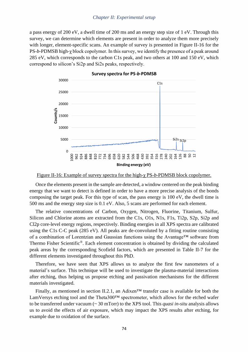
Chapter II: Experimental setup
74
a pass energy of 200 eV, a dwell time of 200 ms and an energy step size of 1 eV. Through this
survey, we can determine which elements are present in order to analyze them more precisely
with longer, element-specific scans. An example of survey is presented in Figure II-16 for the
PS-b-PDMSB high-χ block copolymer. In this survey, we identify the presence of a peak around
285 eV, which corresponds to the carbon C1s peak, and two others at 100 and 150 eV, which
correspond to silicon’s Si2p and Si2s peaks, respectively.
Figure II-16: Example of survey spectra for the high-χ PS-b-PDMSB block copolymer.
Once the elements present in the sample are detected, a window centered on the peak binding
energy that we want to detect is defined in order to have a more precise analysis of the bonds
composing the target peak. For this type of scan, the pass energy is 100 eV, the dwell time is
500 ms and the energy step size is 0.1 eV. Also, 5 scans are performed for each element.
The relative concentrations of Carbon, Oxygen, Nitrogen, Fluorine, Titanium, Sulfur,
Silicon and Chlorine atoms are extracted from the C1s, O1s, N1s, F1s, Ti2p, S2p, Si2p and
Cl2p core-level energy regions, respectively. Binding energies in all XPS spectra are calibrated
using the C1s C-C peak (285 eV). All peaks are de-convoluted by a fitting routine consisting
of a combination of Lorentzian and Gaussian functions using the Avantage™ software from
Thermo Fisher Scientific®. Each element concentration is obtained by dividing the calculated
peak areas by the corresponding Scofield factors, which are presented in Table II-7 for the
different elements investigated throughout this PhD.
Therefore, we have seen that XPS allows us to analyze the first few nanometers of a
material’s surface. This technique will be used to investigate the plasma-material interactions
after etching, thus helping us propose etching and passivation mechanisms for the different
materials investigated.
Finally, as mentioned in section II.2.1, an Adixen™ transfer case is available for both the
LamVersys etching tool and the Theta300™ spectrometer, which allows for the etched wafer
to be transferred under vacuum (~ 30 mTorr) to the XPS tool. This quasi in-situ analysis allows
us to avoid the effects of air exposure, which may impact the XPS results after etching, for
example due to oxidation of the surface.
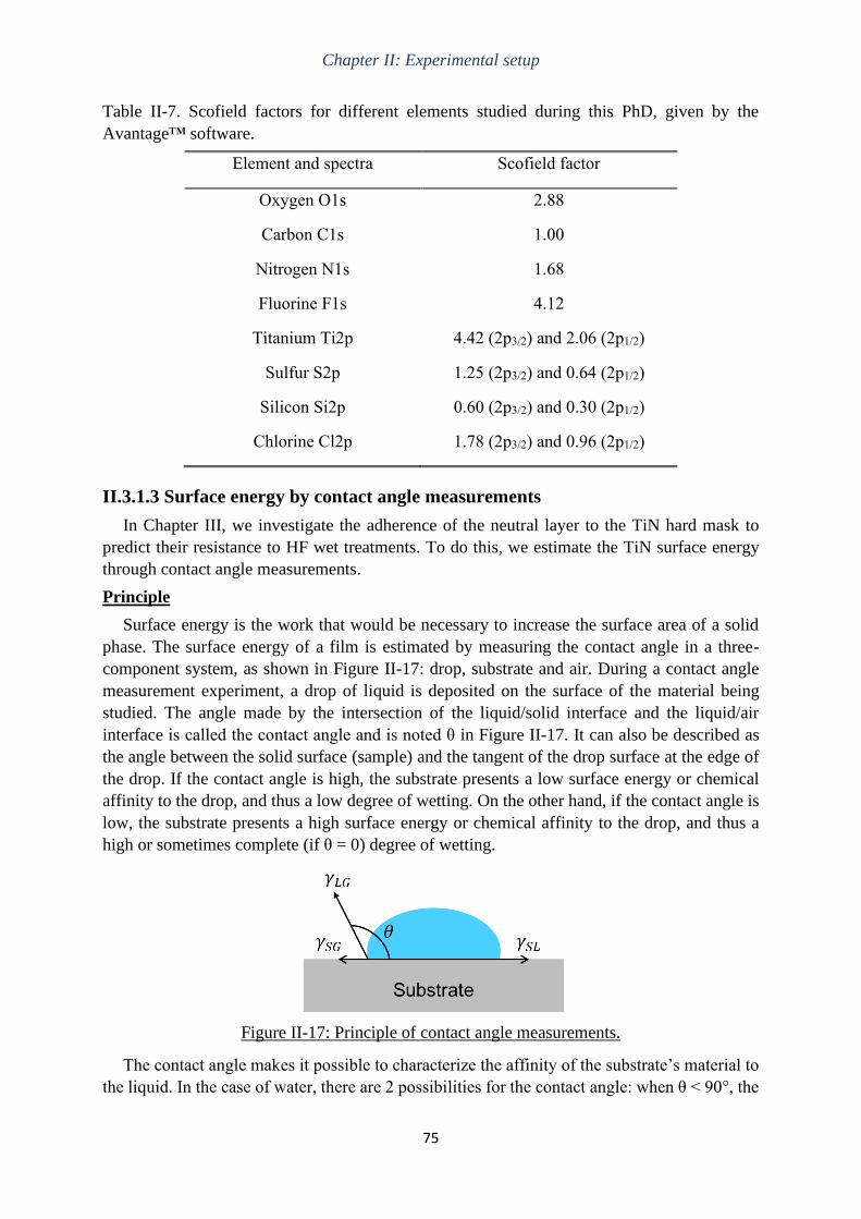
Chapter II: Experimental setup
75
Table II-7. Scofield factors for different elements studied during this PhD, given by the
Avantage™ software.
Element and spectra Scofield factor
Oxygen O1s 2.88
Carbon C1s 1.00
Nitrogen N1s 1.68
Fluorine F1s 4.12
Titanium Ti2p 4.42 (2p3/2) and 2.06 (2p1/2)
Sulfur S2p 1.25 (2p3/2) and 0.64 (2p1/2)
Silicon Si2p 0.60 (2p3/2) and 0.30 (2p1/2)
Chlorine Cl2p 1.78 (2p3/2) and 0.96 (2p1/2)
II.3.1.3 Surface energy by contact angle measurements
In Chapter III, we investigate the adherence of the neutral layer to the TiN hard mask to
predict their resistance to HF wet treatments. To do this, we estimate the TiN surface energy
through contact angle measurements.
Principle
Surface energy is the work that would be necessary to increase the surface area of a solid
phase. The surface energy of a film is estimated by measuring the contact angle in a three-
component system, as shown in Figure II-17: drop, substrate and air. During a contact angle
measurement experiment, a drop of liquid is deposited on the surface of the material being
studied. The angle made by the intersection of the liquid/solid interface and the liquid/air
interface is called the contact angle and is noted θ in Figure II-17. It can also be described as
the angle between the solid surface (sample) and the tangent of the drop surface at the edge of
the drop. If the contact angle is high, the substrate presents a low surface energy or chemical
affinity to the drop, and thus a low degree of wetting. On the other hand, if the contact angle is
low, the substrate presents a high surface energy or chemical affinity to the drop, and thus a
high or sometimes complete (if θ = 0) degree of wetting.
Figure II-17: Principle of contact angle measurements.
The contact angle makes it possible to characterize the affinity of the substrate’s material to
the liquid. In the case of water, there are 2 possibilities for the contact angle: when θ < 90°, the

Chapter II: Experimental setup
76
material is hydrophilic, and when θ > 90°, the substrate is hydrophobic. In order to estimate the
surface energy of the substrate, however, it is necessary to evaluate the contact angle for liquids
with different densities and viscosities.
To determine the surface energy, we use Young's equation, which relates the interfacial
tensions to each other and to the contact angle θ, according to the following equation:
γ𝑆𝐺 = γ𝑆𝐿 + γ𝐿𝐺 × cos(𝜃)
Equation II-14: Young’s equation to obtain the surface energy of a solid.
Where γSG is the solid-air interfacial tension; γSL is the solid-liquid interfacial tension and
γLG is the liquid-air interfacial tension, as shown in Figure II-17. Only γLG is known and θ is
measurable, and thus can be determined during the contact angle measurements. Therefore, in
order to estimate the two unknowns, which are the interfacial tension γSL and the surface tension
of the material γSG, many models have been proposed throughout the years. Some examples of
well-known models are the OWRK (Owens, Wendt, Rabel and Kaelble), Fowkes and Zisman
[OWRK 1969] [Fowkes 1964] [Zisman 1964].
Tool setup
The experimental setup for measuring the contact angles consists of a light source, a camera
(connected to a computer) and a syringe to dispense the drops, as shown in Figure II-18. The
tool used is the drop shape analyzer DSA100 from Krüss. The contact angle measurements
were carried out on small samples of 5 cm x 7 cm.
Figure II-18: Tool setup for contact angle measurements.
Three liquids were used to determine the surface energy of the substrate: water (d = 1 g/cm3);
ethylene glycol (d = 1.1 g/cm3); and diiodomethane (d = 3.3 g/cm3). The use of these three
liquids makes it possible to estimate the surface energy (γ) of the substrate, as well as its
dispersive (γd) and polar (γp) components. For each liquid, 10 drops are deposited and measured
to ensure the reproducibility of the measurement. The drop deposition conditions for each
solvent are presented in Table II-8.
Table II-8. Deposition parameters of the liquids used for the contact angle measurements.
Solvent Flow (µL/s) Volume (µL)
Water 3 2
Ethylene glycol 4 3
Diiodomethane 2 1.5

Chapter II: Experimental setup
77
Data analysis
Based on the measured contact angles obtained for each liquid, it is possible to determine
the surface energy of the substrate. For this, the OWRK method is retained, since it allows
obtaining a total surface energy value, as a function of polar and dispersive components, via a
linear regression on the polar and dispersive energy values obtained for the three liquids. The
OWRK method is represented by Equation II-15:
(1 + cos 𝜃) × γ𝐿𝐺 = 2 × (√γ𝑆𝐺𝑑 γ𝐿𝐺
𝑑 +√γ𝑆𝐺𝑝 γ𝐿𝐺
𝑝 )
Equation II-15: Owens, Wendt, Rabel and Kaelble (OWRK) equation for the surface energy.
Where γd and γp, respectively, represent the dispersive component and the polar component
of the material or liquid. These values are given by the literature for the three liquids (Table II-
9) and can be determined for the solid thanks to a linear regression, which represents the OWRK
function in the form 𝑦 = 𝑎𝑥 + 𝑏:
𝛾𝐿𝐺 × (1 + 𝑐𝑜𝑠𝜃)
2 × √𝛾𝐿𝐺𝑑
⏟ 𝑦
= √𝛾𝑆𝐺𝑝
⏟ 𝑎
×√𝛾𝐿𝐺𝑝
𝛾𝐿𝐺𝑑
⏟𝑥
+√𝛾𝑆𝐺𝑑
⏟𝑏
Equation II-16: Owens, Wendt, Rabel and Kaelble (OWRK) equation in the linear form.
Since γLG, γdLG and γp
LG are known for each liquid and θ is the measured contact angle, the
polar and dispersive components of the substrate’s surface energy are determined by 𝑎2 = 𝛾𝑆𝐺𝑝
and 𝑏2 = 𝛾𝑆𝐺𝑑 . Finally, the surface energy of the material is given by the sum of both
components, so that 𝛾𝑆𝐺𝑝 + 𝛾𝑆𝐺
𝑑 = 𝛾𝑆𝐺 .
The surface energy measurement is commonly used in the microelectronics field, although
it may be considered less reliable than other characterization techniques due to the many
uncertainties that can accompany the result, such as a change in manipulator, device, or surface
preparation. The tool used during this PhD gives a measurement uncertainty of the surface
energy varying, depending on the materials, from 1 to more than 10 mN/m.
Table II-9. Surface energy, as well as its dispersive and polar components, of different liquids.
Solvent Surface energy γ
(mN/m)
Polar component γp
(mN/m)
Dispersive component γd
(mN/m)
Water 72.8 46.4 26.4
Ethylene glycol 47.7 21.3 26.4
Diiodomethane 50.8 2.3 48.5
II.3.1.4 Fourier-Transform Infrared (FTIR) Spectroscopy
Fourier-transform infrared (FTIR) spectroscopy is a chemical characterization technique for
both organic and inorganic materials. It is based on measuring the absorption of infrared
radiation by the sample. Once the raw data is obtained, a Fourier transform is necessary to
convert them into spectral results [Griffiths 2007].

Chapter II: Experimental setup
78
All molecules are made up of atoms linked by chemical bonds. The movement of these atoms
can be regarded as being composed of two components: the stretching and bending vibrations.
Similarly to what we have seen for XPS, the frequencies of these atomic vibrations depend on
the nature of the bonds and also on their chemical environment (interaction with neighboring
atoms). If an electromagnetic wave (infrared beam) strikes the bonds, their vibrations will
increase in amplitude. During FTIR analysis, the sample is illuminated by an infrared beam
with wavenumbers between 400 and 5000 cm-1 and the detector measures how much of that
beam is absorbed by the sample. Since the vibrational energy levels of a molecule are quantized,
only the infrared beam with a frequency exactly corresponding to that required to raise the
energy level of a bond will be absorbed, so the amplitude of that particular vibration is increased
by a certain amount and not gradually. Next, the infrared beam is modified to contain a different
combination of frequencies. This process is rapidly repeated many times over a short time span.
When the sample is irradiated by an infrared beam whose frequency is changed continuously,
the molecule will absorb certain frequencies as the energy is consumed in stretching or bending
different bonds. Then, a computer takes all this data and uses Fourier transforms to determine
the absorption at each wavelength. The transmitted beam corresponding to the region of
absorption will be weakened, and thus a recording of the intensity of the transmitted infrared
beam versus wavenumbers will give a curve showing absorption bands. This is the infrared
spectrum [Nakanishi 1977].
Therefore, by analyzing the beam transmitted through the sample with a spectrometer, the
nature of the chemical bonds can be determined. The recorded signal is the transmittance (T),
that is, the intensity of the transmitted beam (I) divided by the intensity of the incident beam
(I0) as a function of the wavenumber (λ). The absorbance spectrum (A) is then calculated by the
formula 𝐴 = −𝑙𝑜𝑔𝑇. According to the Beer-Lambert law, the areas of the absorbance peaks
are proportional to the concentration of the corresponding bonds. Figure II-19 shows an
example of absorbance spectrum obtained through FTIR for a PS homopolymer, as well as a
table detailing the corresponding bonds for each peak observed.
Figure II-19: Example of FTIR spectrum for a PS homopolymer and table with the
corresponding bonds for each peak observed.

Chapter II: Experimental setup
79
For the PS homopolymer, the absorption bands from 700 to 827 cm-1 correspond to out-of-
plane bending vibrations of the hydrogen atoms bound to the aromatic ring. The band at 1109
cm-1 corresponds to the stretching vibrations of the oxygen in the interstices of Si (Si–O bonds),
which is characteristic of the silicon substrate and unrelated to the PS. The band at 1245 cm-1
might correspond to the stretching vibrations of oxygen bound to carbon (C–O), which probably
comes from air exposure. Next, the absorption band from 1450 to 1606 cm-1 corresponds to the
phenyl ring stretching vibrations. The band at 2339 cm-1 is characteristic of the CO2 from air
exposure. The bands at 2854 and 2923 cm-1 characterize the C–H bond stretching vibrations of
the –CH2– groups. Finally, the band at 3028 cm-1 represents the C–H aromatic stretching
vibration (HC=CH) [Nakanishi 1977].
In Chapter IV, FTIR analysis are carried out on PS and PMMA homopolymers to determine
the influence of UV exposure on their chemical structure. The FTIR measurements were
conducted on a Vertex 70v spectrometer from Bruker. A reference silicon sample is used to
create the background spectra. Finally, all spectra are normalized based on the thickness of the
samples.
II.3.1.5 Time-of-Flight Secondary Ion Mass Spectrometry (ToF-SIMS)
Time-of-Flight Secondary Ion Mass Spectroscopy (SIMS) is a surface analytical technique
which allows us to trace the concentration profile of different species in thin films with
thickness ranging from 0.5 nm to around 100 nm. This technique combines the analytical
technique SIMS (Secondary Ion Mass Spectrometry) with Time-of-Flight mass analysis (TOF).
It provides detailed elemental and molecular information about the sample’s surface, thin layers
and interfaces. It is a very sensitive technique, for which lateral resolution can reach 50 nm,
depth resolution is around 1 nm and mass detection limit is of the order of 1 ppm/μm3
[Vickerman 2001].
During analysis, primary ions are produced by an ion source before being accelerated
towards the sample with a known energy (in keV). Thus, the sample is bombarded by these
primary ions, which then transfer their energy to the sample’s atoms via atomic collisions,
generating a collision cascade, as shown in Figure II-20(a). This energy allows surface atoms
and molecular compounds to overcome the surface binding energy. It should be noticed that the
ion dose is kept low to minimize chemical damage to the sample. Thus, the interaction of the
collision cascade with the surface molecules is soft enough to allow even large and non-volatile
molecules to escape without or with little fragmentation.
Figure II-20: (a) Schematic of the collision cascade, showing the desorption of atoms and
molecules due to primary ion bombardment; and (b) schematic of the time-of-flight mass
analyzer, which separates the secondary ions based on their mass determined by their time-of-
flight. Adapted from [NIST 2021].

Chapter II: Experimental setup
80
Due to the collision cascade, the ejected matter is composed of atoms, emitted ions, and
neutral and ionic clusters. However, only the emitted ions – also known as secondary ions – are
analyzed in this technique. A time-of-flight analyzer is then used. ToF mass spectrometry is
based on the fact that ions with the same energy but different masses travel with different speed.
An electrostatic field accelerates the generated ions to a common energy. Thus, the secondary
ions are extracted from the surface of the sample with a known extraction potential, represented
as Vext in Figure II-20(b). The secondary ions are therefore accelerated towards a mass analyzer,
traveling over a drift path with a speed (v) obtained according to the following equation, where
q is the ion charge and m is the ion mass:
𝑞 × 𝑉𝑒𝑥𝑡 = 𝑚 × 𝑣2
2
Equation II-17: Conservation of energy of the secondary ions.
By replacing the ion speed (v) by the ratio between the distance traveled by the ions (d) and
the time-of-flight (t), so that 𝑣 = 𝑑
𝑡, we obtain the following equation for the time-of-flight as
a function of the ion’s mass:
𝑡 = 𝑑 × √𝑚
2𝑞𝑉𝑒𝑥𝑡=> 𝑡 ∝ √𝑚
Equation II-18: Time-of-flight (t) as a function of the secondary ion’s mass (m).
From Equations II-17 and II-18, we observe that lighter ions fly with a higher speed and
arrive at the detector before the heavier ions. Measuring the time-of-flight for each ion allows
the determination of its mass, thus making it possible to distinguish the different ions according
to their masses in order to then obtain the mass spectrum. This cycle is repeated with a repetition
rate of up to 50 kHz.
Furthermore, the time during which the extraction field is switched off can be used to apply
a low energy secondary ion beam for sample erosion. This analysis mode is known as “dual
beam depth profiling”, since the low energy secondary beam forms a sputter crater, and the
center of this crater is analyzed by the pulsed primary ion beam. During the analysis, the
evolution of the signal is followed according to the penetration depth into the substrate by
alternating erosion and analysis phases. It is therefore possible to obtain several types of
information:
- A mass spectrum, presenting the different chemical elements contained in the layer.
- A depth profile, which gives an evolution of the species according to the depth (the mass
of the species is fixed in this case).
- A 2D map, which shows the mass distribution by rastering a fine-focused ion beam over
the surface of the sample (the mass and the depth are fixed in this case).
In Chapter III, ToF-SIMS analysis are used to complement the results obtained through XPS
and to identify light ions (hydrogen and helium). They were carried out on a ToF-SIMS5 tool
from the company Ion-TOF. The dual beam depth profiling mode was used. Sample erosion
was carried out by a low energy (500 eV) Cs+ ion beam with a raster size of 300 μm. The
analysis beam used is made up of Bi+ ions with an energy of 25 keV, a frame size of 90 x 90
μm2 and an ion dose of 3.87 x 10¹³ ions/cm².

Chapter II: Experimental setup
81
II.3.2 Morphological characterization
This section shall focus on morphological characterization techniques. These
characterization methods, namely the Scanning Electron Microscopy (SEM) and the
Transmission Electron Microscopy (TEM), were used to observe the profile of different
materials after etching. They allow us to measure the thickness and critical dimension (CD) of
the patterns, as well as evaluate the quality of the slope, the roughness, and the presence of
defects.
II.3.2.1 Scanning electron microscopy (SEM)
Throughout this thesis, two types of Scanning Electron Microscopes were used: a SEM
allowing top-view imaging, also known as CD-SEM for Critical Dimension-SEM, and another
allowing cross-sectional imaging. Scanning Electron Microscopy provides information on the
dimensions of the structures observed and, in the case of cross-section images, on the
thicknesses of the different layers of a sample.
Principle
The scanning electron microscopy is based on the following principle: an electronic probe
emits an electron beam, which is strongly accelerated with an energy between 0.1 and 30 kV.
Thanks to an array of electromagnetic lenses, this beam is focused on the sample, and scans the
surface to be observed. During the interaction between the incident electrons and the sample,
elastic and inelastic collisions take place. These interactions lead to different types of emission,
namely the emission of secondary and backscattered electrons, which can give a certain amount
of information on the sample, in the form of images.
- The emission of secondary electrons (SE) comes from the inelastic collisions between the
primary electron (from the incident beam) and the electrons of the valence shells of the atoms
present in the sample, as shown in Figure II-21(a). During the collision, the primary electron
loses energy and its trajectory can be modified. Moreover, this inelastic collision gives little
energy (between 0 and 50 eV) to the secondary electrons to extract themselves from the surface.
Thus, only the secondary electrons emitted by atoms present in the superficial layers close to
the surface can be collected by the detector. This means SE imaging is very sensitive to
variations in the surface morphology and topography of the sample, and the slightest surface
defect will have an impact on the quantity of electrons collected. By scanning the surface, an
electron detector transcribes the electron flux into luminosity and the signal is collected and
synchronized to reconstruct an image faithful to the surface with a topographical effect.
- The emission of backscattered electrons (BSE) is based on the elastic interaction of the
primary electrons of the incident beam with the nuclei of atoms in the sample, as shown in
Figure II-21(b). This results in a random deviation from its initial path, without loss of energy,
also known as elastic diffusion. Since there is no energy loss, the backscattered electrons have
a high energy and can be detected at a much greater depth in the sample, compared to secondary
electrons. Therefore, backscattered electrons are very sensitive to the atomic number (Z) of the
atoms they pass through, which gives an image of the observed surface based on chemical
contrast instead of topography. The higher the atomic number of the atom observed, the more
its number of protons gives it the ability to re-emit electrons in large quantities. Thus, regions
composed of atoms with a high atomic number will appear brighter than others with lower
atomic numbers.

Chapter II: Experimental setup
82
Figure II-21: Schematic representation of the interaction between the primary electron (PE)
and the sample, leading to (a) inelastic collisions that generate the secondary electrons (SE)
and (b) elastic collisions that generate the backscattered electrons (BSE).
Tool setup
Two different SEM tools were used for morphological observations during this PhD. The
critical dimension SEM (CD-SEM) used for top-view observation is the VeritySEM 6i™ tool
from Applied Materials®. SEM images are acquired with an accelerating voltage of 800V and
a probe current of 10 pA. The CD-SEM observation is non-destructive, and no sample
preparation is required. An example of top-view SEM image of a block copolymer assembled
on free surface is shown in Figure II-22(a).
After top-view observations, the cross-section SEM tool used is a Hitachi® S5500™
microscope. It complements the information provided by the top-view observation, since it
consists of obtaining cross-sectional images of the sample, allowing us to measure the CD, the
slope of the sidewalls, the thickness of the stack after etching and the remaining materials at the
bottom of the wafer (if they exist), for example. However, this technique is destructive, since
the wafer must be cleaved to prepare the samples.
Furthermore, cross-sectional samples of polymeric materials are precoated with a platinum
metallization for 30 seconds to reduce charging effects characteristic of the polymer reaction to
the electron beam. All cross-section images are acquired with an accelerating voltage of 5.0 kV,
a probe current of 15 μA and using a tilt of -20°. An example of cross-section SEM image after
removal of one of the blocks of the PS-b-PMMA block copolymer is shown in Figure II-22(b).
Figure II-22: Examples of (a) top-view and (b) cross-section SEM images of a PS-b-PMMA
block copolymer after PMMA removal.

Chapter II: Experimental setup
83
II.3.2.2 Transmission electron microscopy (TEM)
Transmission Electron Microscopy (TEM) is a morphological characterization technique
that gives better resolution than SEM. In fact, the latest generation tools can achieve resolutions
of the order of 90 to 200 pm.
Prior to imaging, samples are prepared using a Focused Ion Beam (FIB). This
micromachining technique etches the material due to high energy ion bombardment (usually
Gallium, Ga+), thus creating cross-sections of approximately 1µm in a specific area of a pattern.
In addition, the sample is thinned to less than 100 nm and a gas, such as tungsten hexacarbonyl
[W(CO)6], is introduced to the vacuum chamber and allowed to chemisorb onto the sample.
Next, the thinned sample is scanned by an electron beam. When scanning the sample with the
beam, the precursor gas is decomposed into volatile and non-volatile components. Since it is a
non-volatile component, the tungsten remains on the surface, thus forming a protection layer to
reduce the impact of the imaging beam on the sample.
The electrons transmitted through the sample are analyzed by various detectors, allowing the
formation of an image. The sample image is projected onto a fluorescent screen that transforms
the electronic image, sensitive to transmission contrast, into an optical image. The contrast
obtained gives information on both the atoms of the sample and the structural defects in the
lattice:
- When the transmitted electrons are collected without diffraction, there is a bright field.
Indeed, electrons that undergo elastic collisions when passing through the sample are deflected
at large angles and are therefore not detected. As the probability of undergoing an elastic
collision increases with the atomic number (Z) of the atoms analyzed, heavier elements appear
darker.
- When the transmitted electrons are collected with diffraction, there is a dark field. This
happens because, when structural defects are present in the lattice, they modify the diffraction
angle.
FIB sample preparation was conducted on a FIB Helios 3 tool from FEI, while TEM analyzes
were performed on a Tecnai Osiris tool, also from FEI, with an electron acceleration voltage of
200 kV. It should be noticed, however, that sample preparation and TEM analysis heavily
impact polymeric materials, such as the block copolymers, leading to shrinkage. Furthermore,
it is also long. Therefore, this technique shall be used sparingly during this PhD, namely to
characterize the pattern profile after spacer etching and SOC removal for the ACE chemo-
epitaxy flow.
Figure II-23: Example of TEM image of a patterned wafer after spacer etching and SOC
removal for the ACE chemo-epitaxy flow.

Chapter II: Experimental setup
84
In this chapter, we have detailed the characteristics of the different polymeric materials
studied throughout this PhD, namely their composition and deposition parameters. We have
also presented the properties of the different etching reactors, both ICP and CCP, used to
study the plasma etching of the high-χ block copolymers; as well as the wet etching tool
used for understanding the interaction between plasma etching, the hard mask and the
neutral layer during the ACE chemo-epitaxy process. Finally, we have explained the
principle of several characterization tools used during this thesis to evaluate and understand
the results obtained in the next three chapters, detailing the experimental setup and data
analysis when applicable.

85
CHAPTER III: ETCHING IMPACT ON THE ACE
CHEMO-EPITAXY FLOW FOR DIRECTED
SELF-ASSEMBLY

Chapter III: Etching impact on the ACE chemo-epitaxy flow for Directed Self-Assembly
86
III. ETCHING IMPACT ON THE ACE CHEMO-EPITAXY
FLOW FOR DIRECTED SELF-ASSEMBLY
We have seen in the introduction chapter that the Directed Self-Assembly of block
copolymers is one of the advanced patterning techniques being considered for obtaining small
and dense patterns with dimensions inferior to 20 nm. This choice is particularly motivated by
the use of well-known lithography steps and by its low cost compared to other solutions.
Different integrations have been proposed to obtain patterns by guiding the self-assembly of
the block copolymers, as shown in Chapter I.3.3. The main difference between them was the
use of either topographical (grapho-epitaxy) or chemical affinity (chemo-epitaxy) constraints,
as well as the commensurability rules for each integration flow presented. In the introduction,
we also outlined the chemo-epitaxy integration developed at CEA Leti, known as “ACE” for
Arkema-CEA, which shall serve as the basis for this chapter.
The ACE flow includes several wet and plasma etching steps. The purpose of this chapter is
therefore to investigate and understand the impact that the different etching steps of the ACE
flow have on the assembly of the block copolymer. Indeed, through its chemistry or other
parameters, the etching steps may modify the surface properties of the hard mask or the neutral
layer, therefore having an effect on the block copolymer’s alignment, notably in terms of
defectivity.
Part of the work presented in this Chapter has been published in the Journal of Vacuum
Science & Technology A [Gusmão 2021].
III.1 ACE chemo-epitaxy flow
In this part, we will present in more detail the ACE integration flow, which was discussed
in the introduction and used as the process of reference at the beginning of this PhD. As we can
see in Figure III-1, this integration starts with an immersion lithography on a trilayer composed
of a photoresist, an anti-reflective layer and a spin-on carbon layer (1-2). The spin-on carbon
serves as a mandrel (3), over which a silicon nitride film is deposited (4) in a conformal manner
and then etched to define the spacers (5-6). The neutral layer is deposited between the spacers
(7) before they are removed to form the narrow guiding stripes (8). Finally, the guiding layer is
grafted to the TiN surface where the spacers are no longer present (9) and the block copolymer
is self-assembled and directed by one of the block’s affinity to the guiding layer (10).
Table III-1 shows the plasma parameters for the different dry etching steps of the flow. All
plasma etching steps correspond to the best chemistries developed at CEA Leti and have been
carried out on a 300 mm Kiyo FX® inductively coupled plasma (ICP) reactor from
LamResearch®, which has been presented in Chapter II.2.1.2.

Chapter III: Etching impact on the ACE chemo-epitaxy flow for Directed Self-Assembly
87
Figure III-1: ACE process flow schematics, consisting of a conventional Self-Aligned Double
Patterning (SADP) process (steps 1 to 6), followed by the DSA process (steps 7 to 10). The
different etching steps have been highlighted by red squares.
Table III-1: Plasma parameters for the different plasma etching steps of the ACE flow. The
etching times correspond to approximately 50% overetch.
Step Chemistry Pressure
(mTorr)
Power
(W)
Bias
(V)
Flow
(ratio)
Time
(s)
2a: SiARC opening CH2F2/SF6/N2/He 5 450 -70 1.5:1:1.5:3 40
2b: SOC opening ME: SO2/O2/He 10 950 -250 3:0.6:1 8
OE: SO2/He 10 950 -250 3:1 17
5: SiN etching CH2F2/CF4/O2 15 500 -400 3:1.5:1 25
6: SOC removal SO2/O2/He 10 950 -250 3:0.6:1 25
The ACE flow consists of the following steps:
(1) Stack preparation
A 100-nm layer of silicon oxide (SiO2) is obtained by thermal oxidation, carried out at
950°C. A 15-nm layer of titanium nitride (TiN) is then deposited over the SiO2 by Physical
Vapor Deposition (PVD) at room temperature under a pressure of 25 mTorr in an ENDURA
300A tool from Applied Materials.
Then, 193 nm immersion lithography is performed on a standard trilayer stack which
consists of, from bottom to top: 73 nm of Spin-On Carbon (SOC), 35 nm of Silicon-containing
Anti-Reflective Coating (SiARC) and 100 nm of lithography photoresist. The SOC and SiARC
are provided by JSR under the trade names HM-8102-9 and ISX534, respectively. The
lithography photoresist used is a negative development resist (NTD) provided by JSR under the
trade name AEX2039, which is annealed at 120°C for 60 seconds before exposure.
Within the framework of the ACE process, the multiplication factor (MF) will be determined
by the lithography pitch (represented only by “Pitch” hereafter) and the intrinsic period of the
BCP (L0). Thus, the notation MFn will be used in the remainder of this manuscript, with 𝑛 =
𝑃𝑖𝑡𝑐ℎ
𝐿0. Figure III-2 shows an example of MF with n = 4 and n = 6.

Chapter III: Etching impact on the ACE chemo-epitaxy flow for Directed Self-Assembly
88
Figure III-2: Schematics for the block copolymer alignment with MF with n = 4 and n = 6.
The table indicates the lithography pitch corresponding to each MF for a block copolymer
with L0 = 32nm.
The 193 nm immersion exposure is carried out on a Twinscan NXT:1970Ci tool from
ASML. The lithography exposure dose is varied for each column. Since the critical dimension
(CD) resolved in the lithography step depends on the dose received by the resist during
exposure, with the dose variation applied to ACE, it is possible to obtain up to 88 different CDs
for a given pitch on the same wafer. After exposure, the substrate is annealed at 90°C for 60
seconds. Finally, the photoresist is developed with n-butyl acetate (NBA) to remove the parts
that were not exposed. The CD of the line patterns obtained in the lithography step are measured
using a CD-SEM before moving to the next step. All the chips in the same column are identical
in terms of CD after lithography as they have been exposed with the same dose.
(2) Trilayer etching: pattern transfer into the SOC layer
The line/space patterns obtained in the previous step are transferred by plasma etching into
the SiARC and SOC layers. As we can see in Table III-1, the SiARC opening step (2a) consists
on a fluorocarbon-based plasma while the SOC opening step (2b) presents a short main etch
(ME) consisting of SO2/O2/He followed by a SO2/He overetch (OE).
Figure III-3: (a) Top-view and (b) cross-section SEM images of the patterns corresponding to
a lithography pitch of 190 nm in the central chip of the wafer (X = 0, Y = 0) after trilayer
etching.
During trilayer etching, a lateral reduction of the lithography CD is observed. For the ACE
flow, this lateral consumption has been measured at approximately 10 nm. Figure III-3 shows
both top-view (a) and cross-section (b) SEM images of the patterns for the central chip on the

Chapter III: Etching impact on the ACE chemo-epitaxy flow for Directed Self-Assembly
89
wafer, with a lithography pitch of 190 nm and a CD of around 73 nm after trilayer etching. The
thickness of the patterns (around 107 nm) corresponds to the SOC + SiARC total thickness.
The profile of the lines is straight except for the SiARC on top of the patterns, which presents
a larger CD (around 78 nm) than the SOC (around 73 nm). As the SiARC will be removed on
the next step, the final CD to be taken into account will be the CD of the SOC mandrel.
(3) SiARC wet etching removal to obtain the SOC mandrel
After pattern transfer into the SOC layer, the SiARC is wet removed with hydrofluoric acid
(HF) diluted to 1% during 15 seconds. The SiARC removal leads to the formation of the SOC
mandrels. The wet removal is conducted on a Raider tool from Semitool®, which has also been
presented in Chapter II.2.2.
(4) SiN spacer deposition
Once the mandrel is formed, a conformal 26-nm layer of silicon nitride (Si3N4, referred to
as SiN for the remainder of this manuscript) is deposited by Plasma-Enhanced Chemical Vapor
Deposition (PECVD) at a temperature of 320°C on a Producer tool from Applied Materials.
Since the SOC degradation temperature is approximately 350°C, the SiN deposition
temperature has been selected in order to avoid the mandrel degradation.
(5) Anisotropic plasma etching of SiN spacer
The SiN layer is anisotropically dry etched in order to form the spacers on the sidewalls of
the mandrel. The parameters for the SiN etching using a CH2F2/CF4/O2 plasma chemistry can
be found in Table III-1 (5). Previous studies have shown that the fluorine-based SiN etching
forms TiF3 particles when left in contact with the TiN hard mask [Posseme 2010], which can
be seen in Figure III-4. Therefore a very short queue time was established between the SiN
etching (step 5) and the SOC removal (step 6), meaning both steps are performed in the same
reactor without air exposure to limit the formation of TiF3 particles.
Figure III-4: Cross-section SEM image of the SOC mandrel and SiN spacers corresponding to
a pitch of 190 nm in the central chip of the wafer (X = 0, Y = 0) after anisotropic SiN etching.
The formation of TiF3 particles on the TiN surface is highlighted.
(6) SOC mandrel removal
The SOC mandrel is removed by SO2/O2/He plasma etching selectively to the SiN, forming
spacers that will later be replaced by the guide patterns for the block copolymer’s self-assembly.
The parameters for the SOC removal can be found in Table III-1 (6).

Chapter III: Etching impact on the ACE chemo-epitaxy flow for Directed Self-Assembly
90
Transmission electron microscopy (TEM) images of the SiN spacers after SOC removal are
presented in Figure III-5. These images confirm the complete removal of the SOC mandrel and
the formation of SiN spacers with CD around 14.5 nm. It should be noticed that the spacer CD
at the interface with the substrate is around 6 nm larger than the top CD. This difference between
top and bottom CD is known as spacer foot. Several solutions to reduce the spacer foot have
been proposed, such as the implantation of light ions (for example, hydrogen or helium) to
modify the SiN bottom layer and facilitate the foot removal [Posseme 2014]. However, they
shall not be addressed during this PhD thesis.
Another important thing to notice is the difference in thickness between the TiN that has
seen all the steps of the ACE flow until now (identified as “TiN A” in Figure III-4) and the TiN
that has been protected by the SOC layer (identified as “TiN B”). This difference can be
explained by the consumption of the TiO2 layer on the “A” zone during steps 1 to 5, namely
due to the ion bombardment of the plasma etching steps (2 and 5) and to the HF wet etching for
SiARC removal (step 3).
Figure III-5: TEM images of the SiN spacers corresponding to a lithography pitch of 190 nm
in the central chip of the wafer (X = 0, Y = 0) after SOC mandrel removal.
(7) Deposition and cross-linking of the neutral layer
The directed self-assembly part of the ACE flow begins by depositing a cross-linkable
neutral layer which will be referred to as “xNL”. This neutral layer is provided by Brewer
Science Inc. and is composed of PS and PMMA. It is deposited by spin-coating in a 300 mm
SCREEN SOKUDO Duo™ coat/develop track to obtain a thickness of around 7.5 nm. It is then
annealed at 250°C for 5 minutes and rinsed using Propylene glycol methyl ether acetate
(PGMEA) in the same track, thus filling the area between the spacers to create a neutral surface.
(8) SiN spacer wet removal
The SiN spacers are then removed by HF diluted to 1% for 60 seconds, creating a vacant
space with a CD equal to half the pitch of the block copolymer, without modifying the physical-

Chapter III: Etching impact on the ACE chemo-epitaxy flow for Directed Self-Assembly
91
chemical properties of the xNL. Once again, the wet removal is conducted on a Raider tool
from Semitool®.
(9) Guide layer grafting
In the space left by the spacers that were removed, a guiding layer provided by Arkema® is
then selectively grafted at 200°C for 75 seconds. A PGMEA rinse allows the removal of
ungrafted polymer chains, thus obtaining the guiding template for the BCP alignment with a
guide layer final thickness of around 7 nm. This grafting is selective, meaning the guide layer
can be grafted onto the TiN hard mask, without grafting onto the xNL.
(10) DSA: block copolymer self-assembly
Finally, the block copolymer is spin-coated and annealed to obtain guided line/space
patterns. The block copolymer used is a PS-b-PMMA provided by Arkema® under the trade
name Nanostrength® EO with an intrinsic period L0 = 32 nm and a lamellar morphology. The
BCP solution is annealed at 240°C for 15 minutes to obtain a film with 33-nm thickness.
Figure III-6 represents the top-view SEM image obtained after the BCP self-assembly step
for the PS-b-PMMA block copolymer with L0 = 32 nm. The PMMA phase is removed through
dry etching to enhance the contrast and facilitate the image capture. Different types of defects
can be seen in this image, like dark spots and BCP alignment defects. These defects are probably
caused by a change in surface properties of the TiN substrate, which is covered by either the
neutral or guide layers. Therefore, the goal of our study shall be to identify the origin of these
defects.
Figure III-6: Top-view SEM image of the PS-b-PMMA block copolymer with L0 = 32 nm
partially aligned by the ACE flow, highlighting the alignment defects and dark spots.

Chapter III: Etching impact on the ACE chemo-epitaxy flow for Directed Self-Assembly
92
III.2 Understanding the effect of etching on the block copolymer’s
alignment
The results presented in Figure III-6 indicate that the surface properties of the TiN hard mask
are not favorable to a perfect alignment of the block copolymer. The goal of this section is to
understand the impact of the etching steps on the TiN surface and identify the ones that mostly
affect its properties, especially regarding its composition and surface energy. We shall also
evaluate the neutral layer’s adherence to the TiN hard mask during HF wet etching as a function
of the etching steps in order to pinpoint the source of the defects.
III.2.1 Effect of the sequence of etching and deposition steps on the TiN
surface
In order to understand the origin of the different defects presented in Figure III-6, the effect
of the sequence of etching and deposition steps on the TiN surface is investigated using TiN
blanket wafers with a 73 nm SOC layer deposited on top, as seen in Figure III-7 (1). For the
trilayer etching, only the last step, corresponding to the SOC opening, is investigated, since it
is the only one that affects the TiN surface. The trilayer etching is conducted using the
parameters presented in Table III-1 (2b). Once the complete removal of the SOC layer is
confirmed by ellipsometry, an HF dip of 15 seconds is also conducted to represent the SiARC
removal. Then, a 26 nm SiN layer is deposited through PECVD as described in the previous
section. Next, the SiN etching and SOC removal are performed using the parameters from Table
III-1 (5, 6). Once again, ellipsometry is used to confirm the complete removal of the SiN layer.
Finally, the TiN surface composition and energy are determined by ex-situ XPS and contact
angle measurements, respectively.
Figure III-7: Sequence of etching and deposition steps applied to TiN blanket wafers.
III.2.1.1 Study of etching steps impact on TiN surface composition
Figure III-8 presents the evolution of O1s (a), N1s (b) and Ti2p (c) ex-situ XPS spectra for
the TiN surface before and after steps 1 to 6. Figure III-8 shows that the TiN surface after steps
1 to 6 presents a strong oxidation when compared to the as deposited TiN surface, with the
increase of TiO2 (Ti2p3/2 peak at around 458.7 eV and O1s peak at 531.6 eV) and decrease of
TiN (Ti2p3/2 peak at around 454.7 eV and N1s peak at 396.9 eV) and Ti-O-N (Ti2p3/2 peak at
around 456.3 eV, N1s peak at 399.6 eV and O1s peak at 530 eV) peaks [Oktay 2015] [Gonbeau
1991]. Figure III-9 summarizes the TiN surface composition determined by XPS before and
after steps 1 to 6. Figure III-9(b) indicates that the TiN surface also presents around 13% of
sulfur after steps 1 to 6, represented by TiOxSy and SO42- with S2p3/2 peaks at 163.4 eV and
169.2 eV, respectively [Gonbeau 1991] [Wagner 1982]. Furthermore, the corresponding O1s
peak at 532.4 eV in Figure III-8(a) also confirmed the presence of SO42- [Salim 2011]. The
presence of fluorine is due to the SiN etching and the presence of carbon is due to contamination
from the reactor walls and to the air exposure between the etching and XPS analysis.

Chapter III: Etching impact on the ACE chemo-epitaxy flow for Directed Self-Assembly
93
Figure III-8: (a) O1s, (b) N1s and (c) Ti2p ex-situ XPS spectra for the TiN surface before and
after the sequence of etching and deposition steps 1 to 6 present on the ACE flow. The results
correspond to an incident angle of 23.75°.

Chapter III: Etching impact on the ACE chemo-epitaxy flow for Directed Self-Assembly
94
Figure III-9: TiN surface composition determined by ex-situ XPS (a) before and (b) after the
sequence of etching and deposition steps 1 to 6 present on the ACE flow. The results
correspond to an incident angle of 23.75°.
III.2.1.2 Contact angle and surface energy measurements
Contact angle measurements are performed on the TiN surface before and after the sequence
of etching and deposition steps. The OWRK method described in Chapter II.3.1.3 is applied to
calculate the surface energy of the TiN surface. The results for the surface energy γ and its
dispersive (γd) and polar (γp) components are summarized in Table III-2, so that:
γ = γ𝑑 + γ𝑝
Equation III-1: The surface energy (γ) corresponds to the sum of its dispersive (γd) and polar
(γp) components.
Previous studies have shown that the surface energy’s polar component is the one that best
indicates the surface affinity between the neutral layer and the substrate [Claveau 2017]. These
studies show that a substrate with a polar component close to 5 mN/m is attractive to the PS-r-
PMMA, which composes the neutral layer used for the ACE process and presents a similar
polar component.
Therefore, it is important to observe that the sequence of etching and deposition steps
presented in Table III-2 induces a significant increase of the surface energy’s polar component,
which goes from 6.5 mN/m for the pristine TiN to approximately 33.5 mN/m for the TiN after
steps 1 to 6. At first glance, this means that the TiN surface is probably not favorable to the
adherence of the neutral layer after the sequence of etching and deposition steps.

Chapter III: Etching impact on the ACE chemo-epitaxy flow for Directed Self-Assembly
95
Table III-2: TiN surface energy before and after the sequence of etching and deposition steps 1
to 6, calculated by contact angle measurements, as well as its dispersive and polar components.
Step Surface energy γ
(mN/m)
Dispersive component
γd (mN/m)
Polar component γp
(mN/m)
As deposited TiN 43.8 37.3 6.5
After steps 1 to 6 78.3 44.8 33.5
III.2.1.3 Effect of the wet spacer removal step on the neutral layer adherence
Following the ACE process flow, the next two steps after SOC removal are the neutral layer
deposition (step 7) and spacer removal through HF wet etching (step 8). The neutral layer
resistance to the HF wet etching is one of the most important parameters that must be verified
in order for the ACE process to work. Failure to conserve the neutral layer after wet etching
might induce various types of self-assembly defects of the block copolymer, such as the ones
presented in Figure III-6.
Therefore, the goal is to verify the adherence of the neutral layer over the TiN surface
modified by the sequence of etching and deposition steps. When the substrate presents the
adequate surface conditions, the neutral layer adheres to the substrate and cannot be removed
through HF dip. For this study, the xNL neutral layer is deposited over the TiN hard mask after
steps 1 to 6, using the conditions described in section III.1(7). The neutral layer thickness after
deposition is measured by ellipsometry. Finally, the 300 mm wafers are submitted to the HF
dip with a 1% dilution using two different times in order to evaluate their impact: 15 and 60
seconds. The neutral layer thickness after HF dip is once again measured by ellipsometry.
Table III-3 presents the results obtained for the neutral layer thickness before and after HF
wet etching for both the pristine TiN surface and the surface after steps 1 to 6 in order to be
able to compare. For the pristine TiN surface, identified as “as deposited”, Table III-3 shows
that the neutral layer thickness is the same before and after HF dip, regardless of its duration,
which means that the surface state of the pristine TiN is favorable to the adherence of the neutral
layer and allows the vertical alignment of the block copolymer during step 10. As shown in
Table III-2, the pristine TiN surface presents a polar component of 6.5 mN/m. Therefore, this
confirms what has been observed in previous studies and was presented in the previous section:
a substrate with a polar component close to 5 mN/m is attractive to the PS-r-PMMA which
composes the neutral layer [Claveau 2017].
Regarding the TiN surface after the sequence of etching and deposition steps 1 to 6, Table
III-3 shows that the neutral layer thickness is reduced from 8.9 to 6.5 nm after HF dip for 15
seconds, meaning the xNL was partially removed during the wet etching. It also shows that
after the longer HF dip of 60 seconds the xNL was completely removed, with its thickness
reduced to zero. Figure III-10 presents cross-section SEM images of the surface after HF dip
for 15 and 60 seconds. After 15 seconds, neutral layer lift-off spots are visible, while after 60
seconds these spots are no longer visible due to the xNL being completely removed. These
results indicate that the TiN surface after the sequence of etching and deposition steps present
in the ACE process is not favorable to the neutral layer’s adherence and, as a result, the neutral
layer is removed through a lift-off process when exposed to a HF dip. Therefore, we can
conclude that the defects observed in Figure III-6 are probably a consequence of the lift-off of

Chapter III: Etching impact on the ACE chemo-epitaxy flow for Directed Self-Assembly
96
the neutral layer during HF dip (step 8). This means the actual sequence of etching steps is not
adapted for the ACE integration flow.
Table III-3. Neutral layer thickness measured by ellipsometry before and after 15 and 60
seconds of HF dip when deposited over the TiN before and after steps 1 to 6.
Neutral layer thickness
(nm)
Before HF
(nm)
After HF for 15s
(nm)
After HF for 60s
(nm)
As deposited TiN 7.0 ± 0.3 7.0 ± 0.3 7.0 ± 0.3
TiN after steps 1 to 6 8.9 ± 1.0 6.5 ± 1.2 0.0 ± 0.0
Figure III-10: Cross-section SEM image of the TiN + xNL surface after steps 1 to 6, neutral
layer deposition and HF wet etching, indicating (a) the neutral layer lift-off spots after HF for
15 seconds and (b) the TiN surface after complete xNL removal using 60 seconds of HF.
In this section, we investigated the impact of the sequence of etching and deposition steps
1 to 6 of the ACE flow on the TiN surface using blanket wafers. XPS analysis showed that,
after the sequence of etching and deposition steps, the TiN surface was highly oxidized and
also presented around 13% of sulfur, represented by TiOxSy and SO42- peaks. Contact angle
measurements were performed to determine the surface energy of TiN. After steps 1 to 6,
we observed that the polar component of the TiN surface energy is five times higher than
the one for the as deposited TiN, which indicated that the TiN surface after the sequence of
etching and deposition steps was probably not favorable to the adherence of the neutral layer.
The next experiment consisted in measuring the neutral layer thickness before and after
HF wet etching. For the neutral layer deposited over non-modified TiN, there was no
difference in thickness before and after HF. However, for the neutral layer deposited over
the TiN after steps 1 to 6, depending on the duration of the HF dip, the neutral layer was
either partially or completely removed. For the partially removed neutral layer, lift-off spots
were observed on the TiN surface. Therefore, we concluded that the defects observed in the
patterned wafer after ACE flow are probably a consequence of the lift-off of the neutral
layer during HF dip. This means the actual sequence of etching steps is not adapted for the
ACE integration flow.

Chapter III: Etching impact on the ACE chemo-epitaxy flow for Directed Self-Assembly
97
III.2.2 Effect of each etching step on the TiN surface
In order to identify which etching step is not adequate for the ACE flow integration, the TiN
blanket wafers have been exposed to each etching step, taken separately: trilayer plasma etching
(step 2b), SiARC removal by HF wet etching (step 3), SiN spacer plasma etching (step 5) and
SOC removal (step 6). Section III.1 already presented the chemistries and parameters used for
each etching step. Figure III-11 presents the initial stack used for each of these studies,
depending on the etching step that is being investigated. The complete removal of the SOC and
SiN layers, when possible, is verified through ellipsometry measurements after etching.
Figure III-11: TiN blanket wafers initial stack used to study each etching step, taken
separately: (a) trilayer or SOC etching; (b) SiARC wet removal; and (c) SiN dry etching.
III.2.2.1 Effect of each etching step on the TiN surface composition
Figure III-12 presents the ex-situ XPS results obtained for the TiN surface before and after
each etching step. Figures III-12(b) and III-12(e) show that the trilayer etching and the SOC
removal present a similar result to the one presented in Figures III-8 and III-9 after the sequence
of steps 1 to 6: strong increase in the oxygen percentage and decrease of the nitrogen percentage
when compared to the pristine TiN surface in Figure III-12(a). This is characterized by the
increase of TiO2 and decrease of TiN and Ti-O-N bonds. They also present a considerable
amount of sulfur, represented by TiOxSy, SO42- and a new S2p3/2 peak at 167.2 eV, which might
correspond to SO2 [Salim 2011]. Together they represent around 12 to 15% of the TiN surface.
As shown before, the presence of carbon and fluorine is due to contamination from the reactor
walls and to the air exposure between the etching and XPS analysis.
Figure III-12 also shows the XPS results after wet etching with HF dip and after SiN spacer
etching with CH2F2/CF4/O2. The surface composition after HF presented in Figure III-12(c) is
quite similar to that of the pristine TiN, with only a very small amount of fluorine present,
represented by a F1s peak at around 684.8 eV, characteristic of metal fluorides, such as TiF3.
Finally, after SiN spacer etching, even though it contains oxygen, the TiN surface was less
oxidized. Indeed, Figure III-12(d) shows that TiN presented a small decrease of around 3 to 7%
each for Ti, N and O percentages. This probably happens because the addition of oxygen to the
fluorocarbon plasma makes it more energetically favorable to form volatile compounds, such
as CO and CO2, rather than a CxFy passivation layer [Mele 1984]. The addition of O2 therefore
increases the concentration of reactive fluorine on the surface of SiN, and thus the formation of
volatile SiF4 can continue without inhibition. The decrease in Ti, N and O percentages is also
proportional to the considerable amount of fluorine (13.5%) present in this sample and
consisting of TiF3.
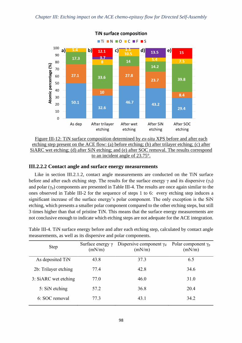
Chapter III: Etching impact on the ACE chemo-epitaxy flow for Directed Self-Assembly
98
Figure III-12: TiN surface composition determined by ex-situ XPS before and after each
etching step present on the ACE flow: (a) before etching; (b) after trilayer etching; (c) after
SiARC wet etching; (d) after SiN etching; and (e) after SOC removal. The results correspond
to an incident angle of 23.75°.
III.2.2.2 Contact angle and surface energy measurements
Like in section III.2.1.2, contact angle measurements are conducted on the TiN surface
before and after each etching step. The results for the surface energy γ and its dispersive (γd)
and polar (γp) components are presented in Table III-4. The results are once again similar to the
ones observed in Table III-2 for the sequence of steps 1 to 6: every etching step induces a
significant increase of the surface energy’s polar component. The only exception is the SiN
etching, which presents a smaller polar component compared to the other etching steps, but still
3 times higher than that of pristine TiN. This means that the surface energy measurements are
not conclusive enough to indicate which etching steps are not adequate for the ACE integration.
Table III-4. TiN surface energy before and after each etching step, calculated by contact angle
measurements, as well as its dispersive and polar components.
Step Surface energy γ
(mN/m)
Dispersive component γd
(mN/m)
Polar component γp
(mN/m)
As deposited TiN 43.8 37.3 6.5
2b: Trilayer etching 77.4 42.8 34.6
3: SiARC wet etching 77.0 46.0 31.0
5: SiN etching 57.2 36.8 20.4
6: SOC removal 77.3 43.1 34.2

Chapter III: Etching impact on the ACE chemo-epitaxy flow for Directed Self-Assembly
99
III.2.2.3 Effect of the wet spacer removal step on the neutral layer adherence
As described in section III.2.1.3, the neutral layer is deposited over the TiN surface after
each etching step and then submitted to a HF wet etching during 60 seconds in order to evaluate
the TiN surface’s compatibility to it. The neutral layer thickness is measured before and after
HF for each case. The results are presented in Table III-5.
First, it is important to notice that the trilayer etching and the SOC removal, which are both
based on SO2/O2/He plasma, are the only steps that present a complete removal of the neutral
layer after HF wet etching. While for the SiARC wet removal by HF and the SiN etching using
a fluorocarbon-based recipe, Table III-5 shows that these steps present the same neutral layer
thickness before and after HF etching.
Table III-5. Neutral layer thickness measured by ellipsometry before and after HF wet etching
for 60 seconds when deposited over the TiN surface after each etching step.
Neutral layer thickness (nm) Before HF (nm) After HF (nm)
TiN after trilayer etching 6.8 ± 0.4 0.0 ± 0.0
TiN after SiARC wet etching 5.8 ± 0.2 5.8 ± 0.2
TiN after SiN etching 5.9 ± 0.3 5.9 ± 0.3
TiN after SOC removal 7.1 ± 0.4 0.0 ± 0.0
The goal of this section was to identify which etching step was not adequate for the ACE
flow integration. Thus, the TiN blanket wafers were exposed to each etching step, taken
separately. The characterization procedure was similar to the one employed in section
III.2.1.
The trilayer etching and the SOC removal, both based on a SO2/O2/He plasma, present
similar results to the sequence of steps 1 to 6: the TiN surface was highly oxidized and
around 14% of sulfur was observed. Moreover, the polar component of the surface energy
was five times higher than the one for the as deposited TiN. Finally, the trilayer etching and
the SOC removal were the only steps that led to a lift-off of the neutral layer during HF wet
etching.
For the SiARC wet etching and the SiN etching, no difference was observed for the
neutral layer thickness before and after HF.
Therefore, based on the different results obtained, we concluded that the neutral layer
lift-off defects observed after the sequence of etching and deposition steps on both patterned
and blanket wafers were most probably caused by the interaction of the SO2/O2/He plasma
with the TiN surface.

Chapter III: Etching impact on the ACE chemo-epitaxy flow for Directed Self-Assembly
100
III.2.3 Understanding the effect of the SO2/O2/He plasma on the TiN surface
and neutral layer deposition
In order to understand the effect of the SO2/O2/He plasma on the TiN surface, each gas is
applied separately to the TiN blanket wafers, using the same plasma parameters presented in
Table III-1(6). Furthermore, the effect of ion bombardment has also been investigated by
applying the SO2/O2/He plasma with zero RF Bias power and keeping the other parameters
constant.
III.2.3.1 Effect of each gas on the TiN surface composition
The ex-situ XPS results for the TiN surface are presented in Figure III-13. First, when
comparing the SO2/O2/He results with the results for each gas, the following is observed: for
the SO2 only presented in Figure III-13(b), the Ti and N percentages are similar to the reference
in Figure III-13(a), while the oxygen content sees a decrease of about 4%, which is
characterized by a slight reduction of the TiO2 peak. The sulfur percentage is also slightly lower
and the SO2 peak at 167.2 eV is no longer present. As for the O2 only, Figure III-13(c) shows a
significant increase of the titanium percentage due to the increase of the TiO2 peak intensity.
There is also an important reduction of the nitrogen percentage, which is represented by the
decrease of the TiN peak intensity. Finally, for the He only in Figure III-13(d), there is an
increase of both Ti and N percentages, characterized by an augmentation of the TiN and Ti-O-
N peaks intensity. It is also possible to observe a decrease of the oxygen percentage,
consequence of the decrease of the TiO2 peak intensity. As expected, sulfur is no longer present
on the TiN surface after O2 only and He only. For all conditions, the carbon, fluorine and
chlorine contamination comes from the etching reactor walls.
Figure III-13: TiN surface composition determined by ex-situ XPS: (a) after SO2/O2/He
(reference); (b) after SO2 only; (c) after O2 only; (d) after He only; and (e) after SO2/O2/He
without RF bias power. The results correspond to an incident angle of 23.75°.
Figure III-13(e) presents the results after etching using SO2/O2/He without RF bias power.
When compared to the results with RF Bias in Figure III-13(a), several changes can be noticed:
the nitrogen content is increased by about 11.6% compared to the same chemistry with bias,

Chapter III: Etching impact on the ACE chemo-epitaxy flow for Directed Self-Assembly
101
which is characterized by an increase of the TiN peak. A significant decrease of the oxygen
percentage of at least 12% is also observed, consequence of the decrease of the TiO2 peak
intensity. Moreover, it shows a slight increase of the Ti percentage, which is a combination of
the TiN peak intensity augmentation and the TiO2 peak intensity reduction. Finally, a sulfur
percentage decrease of 7.2% is observed and the TiOxSy and SO2 peaks are no longer present.
This means that, for the zero bias etching, the thickness of the TiN layer modified by the plasma
is smaller compared to that of the reference SO2/O2/He SOC removal process.
Ion implantation simulations using the software SRIM confirm this observation. For these
simulations, the stack was defined as 150 Å of TiN with 30 Å of TiO2 over it. The ion energy
was varied between 10 and 500 eV, where 10 eV is an approximation for the zero RF bias
condition and 250 eV is an approximation for the SO2/O2/He reference (RF bias = -250 V). For
each condition, 100000 ions have been implanted. The graphs in Figure III-14 represent the
number of sulfur (a) and helium (b) ions implanted for the different energies investigated as a
function of the TiO2 and TiN thickness. For the “zero bias” condition, both sulfur and helium
ions are restrained to the first 10 to 20 Å of the TiO2 layer. However, for the 250 eV condition,
some sulfur ions reach the TiN layer and the total modified thickness is around 40 Å while most
of the helium ions are present in the TiN layer and the total modified thickness corresponds to
approximately 83 Å.
Figure III-14: Simulation showing the effect of different ion energies on the implanted
thickness for (a) sulfur and (b) helium ions on a TiO2 + TiN stack.
Furthermore, Time-of-Flight Secondary Ion Mass Spectrometry (ToF-SIMS) analysis have
also been conducted on these samples to determine the concentration of sulfur, oxygen, fluorine
and chlorine as a function of the sample thickness and compare the results to those obtained
using XPS. Indeed, XPS analysis quantify an element on a larger volume (approximately 10
nm x π x 200 µm x 200 µm) than ToF-SIMS (1 nm x 90 µm x 90 µm). Therefore, XPS analysis
average the signal over 10 nm while ToF-SIMS gives a value within 1-2nm. Moreover, ToF-
SIMS is able to detect light elements, such as helium. However, during our analysis, no helium
was detected, meaning it presented low ionization yield and probably little implantation into
the TiN surface.
The ToF-SIMS results are presented in Figure III-15. The sulfur profile in Figure III-15(a)
confirms what has been indicated by both the ex-situ XPS analysis and the ion implantation
simulation: for the SO2/O2/He with zero bias, the thickness of the modified layer is thinner than
for the same chemistry with -250 V bias.

Chapter III: Etching impact on the ACE chemo-epitaxy flow for Directed Self-Assembly
102
For the oxygen profile presented in Figure III-15(b), due to the O- saturation on the TiN
extreme surface for every sample, we have chosen to use the molecular fragment OH- instead,
whose attribution is the most reliable and whose ionization yields are considered good. The
results are as expected: the O2 only sample presents a thicker TiO2 layer (around 4 nm)
compared to the other samples, followed by SO2/O2/He and SO2 only (around 2 nm). As has
been shown before, the SO2/O2/He without bias presents a thinner modified layer (around 1
nm). The He only sample, however, presents a higher oxygen content than expected based on
the XPS results. One possible explanation for this difference between the two results is the air
exposure duration. While XPS analysis were conducted at the most 5 hours after sample
etching, ToF-SIMS samples waited 24 hours between etching and analysis, meaning they had
more time to oxidize.
Finally, for the fluorine (c) and chlorine (d) profiles, it should be noticed that excess oxygen
increases the ionization yield of Cl- and F- ions, which explains their significant presence in the
O2 only and He only samples. Fluorine and chlorine contamination is also more visible for these
two samples due to the lower total flow when O2 and He are taken separately (maximum 50
sccm). Therefore, the ToF-SIMS results confirm the observations made with XPS.
Figure III-15: ToF-SIMS analysis for (a) sulfur (S-), (b) oxygen (OH-), (c) fluorine (F-) and
(d) chlorine (Cl-) concentration as a function of the sample thickness (depth).
III.2.3.2 Contact angle and surface energy measurements
Contact angle measurements have also been conducted for these samples. Table III-6
presents the surface energy results for the different gases applied individually and for the zero
bias etching. All results are similar to the SO2/O2/He SOC removal, with the surface energy

Chapter III: Etching impact on the ACE chemo-epitaxy flow for Directed Self-Assembly
103
varying between 1 and 3% regarding the reference value (77.3 mN/m). Moreover, the polar
component varies between 1.5 and 14% compared to the SO2/O2/He reference (34.2 mN/m)
and is at least 4 times higher than the pristine TiN polar component (6.5 mN/m). Therefore,
these measures are not conclusive enough for understanding the effect of each gas on the TiN
surface and neutral layer adherence.
Table III-6. TiN surface energy as well as its dispersive and polar components calculated by
contact angle measurement before and after SO2/O2/He, SO2 only, O2 only, He only and
SO2/O2/He without RF bias power.
Etching Surface energy γ
(mN/m)
Dispersive component γd
(mN/m)
Polar component γp
(mN/m)
As deposited TiN 43.8 37.3 6.5
SO2/O2/He 77.3 43.1 34.2
SO2 only 78.4 44.7 33.7
O2 only 74.9 45.6 29.3
He only 79.0 47.2 31.8
SO2/O2/He zero bias 78.3 45.0 33.3
III.2.3.3 Effect of the wet spacer removal step on the neutral layer adherence.
Finally, in order to verify the adherence of the neutral layer over the TiN surface for the
different conditions investigated, the neutral layer deposition and HF wet etching have been
conducted following the same procedure described in the previous sections. The thickness
measurement results are presented in Table III-7. After SO2 only and SO2/O2/He with zero bias,
the neutral layer is almost completely removed after wet etching. As for the O2 only and He
only samples, no significant thickness variation is observed after HF.
Table III-7. Neutral layer thickness measured by ellipsometry before and after 60 seconds of
HF wet etching when deposited over the TiN surface etched using SO2/O2/He, SO2 only, O2
only, He only, and SO2/O2/He without RF bias power.
Neutral layer thickness (nm) Before HF (nm) After HF (nm)
SO2/O2/He 7.1 ± 0.4 0.0 ± 0.0
SO2 only 8.2 ± 0.5 0.5 ± 0.2
O2 only 9.2 ± 0.4 9.3 ± 0.5
He only 6.3 ± 0.6 6.5 ± 1.1
SO2/O2/He zero bias 7.0 ± 0.5 0.9 ± 0.2

Chapter III: Etching impact on the ACE chemo-epitaxy flow for Directed Self-Assembly
104
III.2.4 Understanding the interaction mechanism between SO2/TiN/xNL/HF
that leads to the neutral layer lift-off
Now that we have determined the SO2 to be the main responsible for the xNL lift-off during
HF wet etching, this section shall focus on understanding the interaction mechanisms between
the SO2 plasma, the TiN surface, the xNL deposition and the HF wet etching that ultimately
leads to the lift-off of said neutral layer.
III.2.4.1 Impact of TiN modified layer
We first decided to verify the role of the modified layer that is formed on the TiN surface
after SO2/O2/He SOC removal, which consists of TiO2/TiOxSy/SO42- according to XPS results
previously shown. Our goal is to remove the modified layer before depositing the xNL and then
evaluate the neutral layer adherence. Thus, before xNL deposition, we chose to perform an HF
wet etching, which is known to remove the TiO2 native oxide without removing the TiN,
following the reaction [Lee 2017]:
TiO2 + 4HF → TiF4 + 2H2O (ΔG° = −6.1 kcal/mol at 298 K)
The schematics for this experience can be found in Figure III-16. We used a TiN blanket
wafer on which a 73-nm SOC layer was deposited. The SOC layer was then removed using the
SO2/O2/He plasma. However, before depositing the neutral layer, an HF wet etching was
conducted during 60 seconds to remove the modified TiO2/TiOxSy/SO42- layer on the TiN
surface. The native TiO2 layer was reformed on the TiN surface right after HF etching due to
the air exposure. Then, the xNL was spin-coated and annealed over the TiN surface and another
HF dip was conducted for 60 seconds after xNL deposition.
In order to understand the effect of the SO2/O2/He plasma on the TiN surface, each gas
was applied separately to the TiN blanket wafers, while keeping the other plasma parameters
constant.
The results led us to conclude that, while the oxygen alone highly oxidizes the TiN
surface and increases its surface energy, it did not have a significant negative effect on the
neutral layer adherence, thus allowing this layer to resist the HF wet etching step. The same
was observed for the helium: based on the ellipsometry measurements, it did not seem to
prevent the adherence of the neutral layer.
The effect of ion bombardment was also investigated by applying the SO2/O2/He plasma
with zero RF Bias power and keeping the other parameters constant. However, this
parameter did not seem to be the most significant either. Without RF Bias, even though the
TiN modified layer was thinner when compared to the same process with Bias, the neutral
layer was still almost completely removed, which means the SO2/O2/He SOC removal
chemistry is not adapted to the chemo-epitaxy application.
Finally, it was the SO2 alone that presented the TiN surface composition the most similar
to the TiN after SO2/O2/He. It also failed to conserve the neutral layer during HF wet etching,
leading to its lift-off. Therefore, we concluded that the SO2 molecule was the main
responsible for this recipe’s inadequacy to the ACE flow.

Chapter III: Etching impact on the ACE chemo-epitaxy flow for Directed Self-Assembly
105
Figure III-16: Schematics for the experience conducted in order to verify the impact of the
modified layer formed on the TiN surface after SOC etching.
Thickness measurements for the TiN, SOC and neutral layer after each step can be found in
Table III-8. The SOC thickness measurement is used to confirm the complete SOC removal
using the SO2/O2/He plasma (step 2) before moving on to the first HF wet etching (step 3). The
TiN ellipsometry measurements also include the native oxide layer on the TiN surface, as well
as the modified layer after etching. This should explain the larger incertitude in the
measurements observed for TiN (between 1.0 and 1.2 nm) when compared to the SOC and xNL
(around 0.2 nm). Considering the difficulty of fitting for metallic materials such as TiN, along
with the probable change in refractive index of the surface layer before and after etching and
the reduced thickness of the modified TiO2/TiOxSy/SO42- layer estimated to be around 2 or 3
nm, the TiN thickness measurements shall only be used comparatively and cannot be considered
quantitatively accurate.
Nevertheless, after step 3, we observe a decrease on TiN thickness of about 2.1 nm, which
indicates that the TiO2/TiOxSy/SO42- layer has been removed through HF wet etching. Ex-situ
XPS analysis were conducted immediately after the first HF wet etching (step 3) to confirm this
and the results are presented in Figure III-17. When comparing the XPS results after SO2/O2/He
plasma shown in Figure III-17(b) and the ones after the first HF treatment shown in Figure III-
17(c), we are able to confirm the consumption of the modified TiO2/TiOxSy/SO42- layer, since
sulfur is no longer present and the oxygen percentage is decreased by around 30%.
Table III-8. TiN, SOC and neutral layer thicknesses measured by ellipsometry after each step
presented in Figure III-16.
Step TiN thickness (nm) SOC thickness (nm) xNL thickness (nm)
1: Initial stack 18.1 ± 1.0 72.4 ± 0.2 -
2: SO2/O2/He etching 18.2 ± 1.2 0.0 ± 0.0 -
3: HF wet etching 16.1 ± 1.0 - -
4: xNL deposition 17.1 ± 1.0 - 9.6 ± 0.2
5: HF wet etching 17.1 ± 1.0 - 9.7 ± 0.3
Finally, Table III-8 shows that, by introducing an HF wet etching step between the SOC
removal and the xNL deposition, the xNL is not removed by the second HF treatment, which
confirms the negative effect of the TiO2/TiOxSy/SO42- layer on the adhesion of the neutral layer.

Chapter III: Etching impact on the ACE chemo-epitaxy flow for Directed Self-Assembly
106
However, while the addition of an HF wet etching step is one solution to avoid the neutral
layer lift-off issue, it cannot be applied to the ACE chemo-epitaxy flow. Indeed, along with the
TiO2/TiOxSy/SO42- layer, the HF would also remove the SiN spacers before the xNL could be
deposited, thus going against the principles of the ACE integration. Other solutions to avoid
lift-off which are compatible with the ACE flow shall be presented in section III.3.
Figure III-17: TiN surface composition determined by ex-situ XPS: (a) before etching; (b)
after SO2/O2/He plasma; and (c) after SO2/O2/He plasma and HF wet etching. The results
correspond to an incident angle of 23.75°.
III.2.4.2 First hypothesis: H2SO4 formation on the TiN surface
Based on the results obtained until now, we have proposed some mechanism hypothesis for
the neutral layer lift-off and we will verify then over the next three sections.
The schematics for the first hypothesis are presented in Figure III-18. It is based on the
recombination of the H+ ions of the HF with the SO42- ions observed on the surface of the TiN
after any plasma etching based on SO2, therefore forming H2SO4, which could then remove the
neutral layer. The reaction for H2SO4 formation is:
2H+ + SO42- → H2SO4 (ΔG° = −164.1 kcal/mol at 298 K)
Hypothesis #1: SO42− ions on the TiN surface recombine with the H+ ions of the HF wet
etching to form sulfuric acid (H2SO4), which removes the neutral layer.
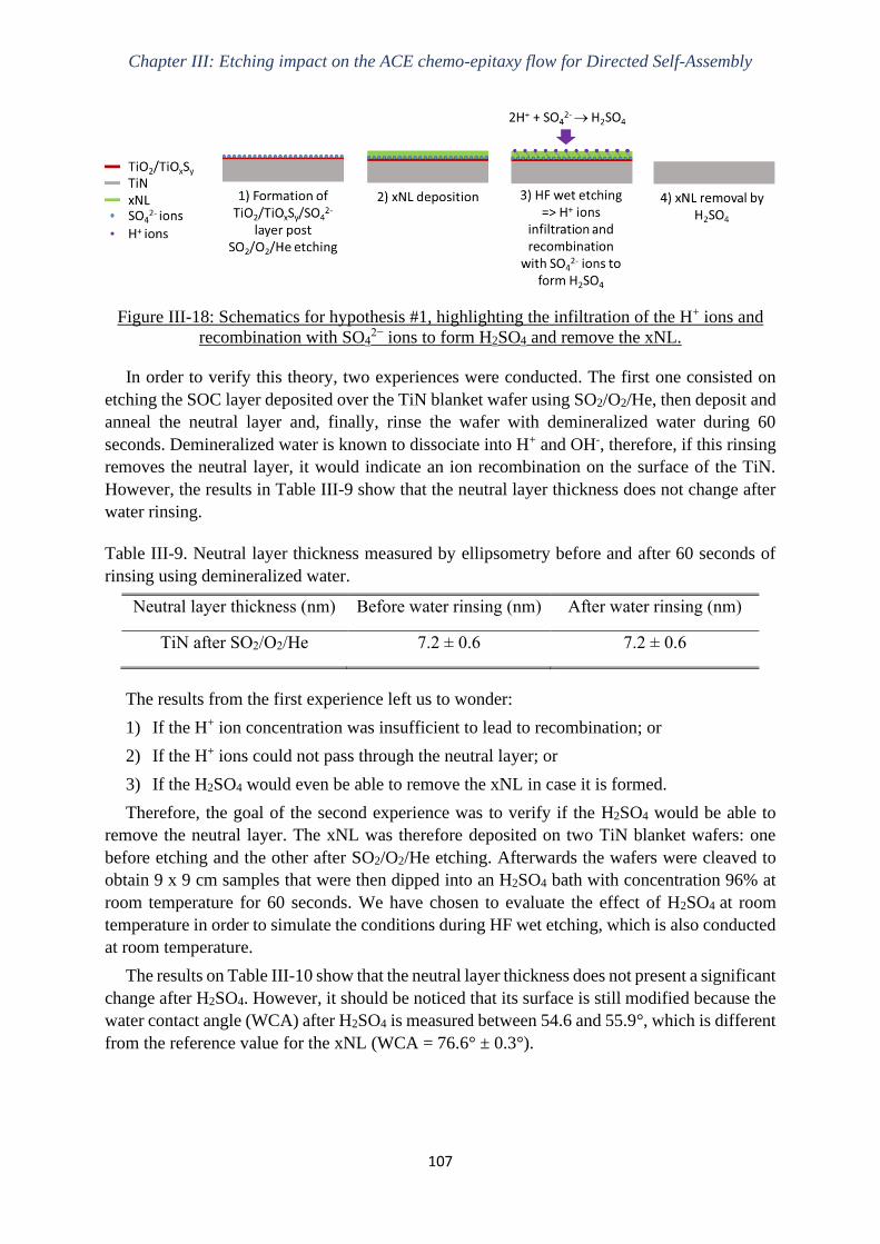
Chapter III: Etching impact on the ACE chemo-epitaxy flow for Directed Self-Assembly
107
Figure III-18: Schematics for hypothesis #1, highlighting the infiltration of the H+ ions and
recombination with SO42− ions to form H2SO4 and remove the xNL.
In order to verify this theory, two experiences were conducted. The first one consisted on
etching the SOC layer deposited over the TiN blanket wafer using SO2/O2/He, then deposit and
anneal the neutral layer and, finally, rinse the wafer with demineralized water during 60
seconds. Demineralized water is known to dissociate into H+ and OH-, therefore, if this rinsing
removes the neutral layer, it would indicate an ion recombination on the surface of the TiN.
However, the results in Table III-9 show that the neutral layer thickness does not change after
water rinsing.
Table III-9. Neutral layer thickness measured by ellipsometry before and after 60 seconds of
rinsing using demineralized water.
Neutral layer thickness (nm) Before water rinsing (nm) After water rinsing (nm)
TiN after SO2/O2/He 7.2 ± 0.6 7.2 ± 0.6
The results from the first experience left us to wonder:
1) If the H+ ion concentration was insufficient to lead to recombination; or
2) If the H+ ions could not pass through the neutral layer; or
3) If the H2SO4 would even be able to remove the xNL in case it is formed.
Therefore, the goal of the second experience was to verify if the H2SO4 would be able to
remove the neutral layer. The xNL was therefore deposited on two TiN blanket wafers: one
before etching and the other after SO2/O2/He etching. Afterwards the wafers were cleaved to
obtain 9 x 9 cm samples that were then dipped into an H2SO4 bath with concentration 96% at
room temperature for 60 seconds. We have chosen to evaluate the effect of H2SO4 at room
temperature in order to simulate the conditions during HF wet etching, which is also conducted
at room temperature.
The results on Table III-10 show that the neutral layer thickness does not present a significant
change after H2SO4. However, it should be noticed that its surface is still modified because the
water contact angle (WCA) after H2SO4 is measured between 54.6 and 55.9°, which is different
from the reference value for the xNL (WCA = 76.6° ± 0.3°).

Chapter III: Etching impact on the ACE chemo-epitaxy flow for Directed Self-Assembly
108
Table III-10. Neutral layer thickness measured by ellipsometry before and after 60 seconds
inside an H2SO4 bath at room temperature, as well as the water contact angle measured after
H2SO4.
Neutral layer thickness (nm) Before H2SO4 (nm) After H2SO4 (nm) WCA after H2SO4
TiN as dep 7.1 ± 0.2 7.5 ± 0.4 55.9° ± 0.4°
TiN after SO2/O2/He 7.3 ± 0.5 7.7 ± 0.6 54.6° ± 0.2°
Figure III-19 shows the cross-section SEM images after H2SO4 during 60 seconds for both
wafers. Due to the neutral layer’s very small thickness and to its sensitivity to the electron beam
from the SEM, it is not possible to measure its real thickness using these SEM images.
Nevertheless, the cross-section images indicate that the xNL surface after H2SO4 is slightly
rough, which may explain the slight increase in thickness (around 0.4 nm) measured by
ellipsometry after H2SO4.
Figure III-19: Cross-section SEM images of the xNL surface after H2SO4 during 60 seconds
for the xNL deposited over TiN (a) before etching; and (b) after SO2/O2/He plasma.
Moreover, we have also evaluated a longer H2SO4 exposure, leaving the wafer inside the
bath for 5 minutes instead of 60 seconds, but the results were similar. These results allow us to
conclude that the H2SO4 does not spontaneously remove the neutral layer at room temperature.
Finally, concerning observation 2 – “can the H+ ions pass through the neutral layer?” –, it
should be noticed that if HF were capable of passing through the cross-linked neutral layer to
interact with the TiN surface, it should remove the TiO2 layer even for other plasma chemistries
and for the pristine TiN. And if it did remove the TiO2, then the xNL should also be removed
through lift-off. However, we have seen in sections III.2.1.3 and III.2.2.3 that in most cases the
xNL resists the HF wet etching, which indicates that the HF does not pass through the neutral
layer in normal conditions. Therefore, based on all the results and observations presented,
hypothesis #1 has been eliminated.
III.2.4.3 Second hypothesis: pore formation on the neutral layer
When Salim et al. studied the preparation of TiO2 nanoparticles from hydrolysis reaction of
TiOSO4, they observed the adsorption of SO42− ions on the surface of TiO2 through XPS

Chapter III: Etching impact on the ACE chemo-epitaxy flow for Directed Self-Assembly
109
analysis. They also observed that the intensity of the XPS peak corresponding to the SO42− ions
decreases with a post-treatment consisting of annealing during 1 hour at 600°C, indicating that
the annealing provides the energy necessary not only for the growth of the grains but also for
the desorption of the residual ions on the surface of the TiO2. Finally, due to this ionic
desorption, internal pores are formed inside the TiO2 nanoparticles [Salim 2011].
Therefore, our second hypothesis is based on the desorption of the SO42- ions – which are
observed on the surface of the TiN after SO2-based etching – during the annealing of the neutral
layer at 250°C. This would form internal pores inside the xNL, thus allowing the HF to pass
through and remove the modified TiO2/TiOxSy layer on the TiN surface. By removing this
modified layer, the neutral layer adherence to the TiN hard mask is reduced, allowing its
consequent lift-off. The schematics for this hypothesis can be found in Figure III-23.
Figure III-20: Schematics for hypothesis #2, highlighting the desorption of SO42− ions during
annealing of the neutral layer and the consequent formation of internal pores inside the xNL.
These pores facilitate the infiltration of the H+ and OH- ions and the removal of the modified
TiO2/TiOxSy layer formed on the TiN surface, thus reducing the neutral layer adherence to the
TiN hard mask and allowing its consequent lift-off.
In order to verify this hypothesis, TiN blanket wafers after SOC removal using SO2/O2/He
are introduced in the Sokudo DUO 300 mm track dedicated to xNL deposition. However,
instead of depositing the neutral layer, one of the wafers goes through the annealing at 250°C
for 5 minutes and is then removed from the track while the other wafer goes through the same
annealing and also the PGMEA rinsing. The surface composition of these wafers is analyzed
Hypothesis #2: desorption of SO42− ions during annealing of the neutral layer could form
pores inside the xNL, which would facilitate the infiltration of the HF. The HF would then
remove the modified TiO2/TiOxSy layer formed on the TiN surface, thus reducing the neutral
layer adherence to the TiN hard mask and allowing its consequent lift-off.

Chapter III: Etching impact on the ACE chemo-epitaxy flow for Directed Self-Assembly
110
through XPS to verify the presence of the SO42- ions after annealing and annealing + rinsing.
The distribution of sulfur S2p peaks on the TiN surface for each sample is shown in Figure III-
21. By comparing the results after etching (a), after annealing (b) and after rinsing (c), there is
no significant variation of the SO42- and TiOxSy percentages while the SO2 is slightly reduced
after annealing and rinsing.
However, when the effect of each gas individually and of the RF bias was evaluated in
section III.2.3, it was observed that for SO2/O2/He without RF bias, the only peak present on
the S2p XPS spectra is the SO42- and still the xNL is partially removed after HF wet etching.
Therefore, the SO2 peak does not seem to be the main responsible for the lift-off of the neutral
layer and its slight reduction in percentage after annealing and rinsing is probably not significant
regarding the neutral layer lift-off.
Figure III-21: Distribution of sulfur S2p peaks on the TiN surface determined by ex-situ XPS
for each sample: (a) after SO2/O2/He etching; (b) after SO2/O2/He etching + annealing at
250°C for 5 minutes; and (c) after SO2/O2/He etching + annealing at 250°C for 5 minutes +
PGMEA rinsing. The results correspond to an incident angle of 23.75°.
Nevertheless, we decided to verify if pores are formed on the surface of the neutral layer by
conducting ellipsometric porosimetry measurements on the xNL deposited over pristine TiN
(identified as “as dep”) and over TiN after SO2/O2/He SOC removal. The samples were placed
under 90% humidity and then the xNL thickness and refractive index were measured as a
function of time (between zero and 60 minutes). For the xNL thickness results presented in
Figure III-22(a), a variation of about 0.15 nm for TiN as dep and 0.6 nm for TiN post SO2/O2/He
plasma is observed. However, measurement fitting turned out to be very complicated because
the xNL and TiN layers are significantly thin and do not necessarily present the same refractive
indices for both samples due to the impact of etching. Therefore, several “solutions”
(thickness/refractive index pairs) were possible each time. Considering the difficulty of fit, it is
hard to determine if the 0.6 nm thickness variation is significant.

Chapter III: Etching impact on the ACE chemo-epitaxy flow for Directed Self-Assembly
111
As for the refractive index (n) measurements, usually if the material is porous, the average
refractive index increases with the water infiltration because it presents a higher refractive index
(nwater = 1.3) when compared to the air (nair = 1.0). The refractive index results at a wavelength
of 632.8 nm are presented in Figure III-22(b) for both samples. For the xNL deposited over
pristine TiN, the refractive index does not vary significantly and the average index is around
1.51. As for the xNL over TiN after SO2/O2/He plasma, the measurements are very noisy and
the refractive index varies between 1.58 and 1.61, but this variation is not constant over time.
Moreover, the average refractive index is at 1.59, which is higher compared to the xNL
deposited over pristine TiN. This could indicate a difference in composition for the xNL
deposited over the etched surface, but once again it is hard to determine if this difference is
significant with the difficulty of fit and the many {thickness/refractive index} pairs possible.
Therefore, while the ellipsometric porosimetry measurements are not entirely conclusive, a
priori they do not indicate the presence of pores on the surface of the xNL. Along with the XPS
results in Figure III-21 that show no desorption of SO42- ions after annealing and rinsing,
hypothesis #2 does not seem to be the most likely explanation for the neutral layer lift-off.
Figure III-22: (a) xNL thickness and (b) refractive index as a function of exposure time
obtained through ellipsometric porosimetry for the xNL deposited over non-etched TiN (“as
dep”) and TiN after SO2/O2/He SOC removal.

Chapter III: Etching impact on the ACE chemo-epitaxy flow for Directed Self-Assembly
112
III.2.4.4 Third hypothesis: disruption of the neutral layer’s cross-linking
Our third hypothesis is based on an interaction between the SO42- ions and the cross-linking
agent of the neutral layer. The SO42- ions would disrupt the complete cross-linking of the xNL,
allowing for a path to form, through which the HF would be able to cross and react with the
modified TiO2/TiOxSy layer on the TiN surface. The HF would then remove the modified
TiO2/TiOxSy layer, which would reduce the neutral layer adherence to the TiN hard mask and
allow its consequent lift-off.
Since the cross-linking agent’s composition and its cross-liking kinetics are not known due
to confidentiality reasons, this hypothesis is harder to verify than the previous ones.
Nevertheless, we have investigated the impact of the xNL deposition parameters, namely
thickness and annealing time, on its adherence to the TiN surface after SO2/O2/He SOC
removal.
First, we decided to evaluate the influence of the TiN/xNL interface on the lift-off
phenomenon. By increasing the xNL thickness, we are able to reduce the influence of the
TiN/xNL interface on the bulk material and, therefore, possibly avoid the lift-off. To obtain a
thicker xNL, we have to decrease the spin-coating speed. The reference spin-coating speed for
the xNL is 1500 rpm (revolutions per minute), which leads to a thickness of around 7.5 nm. In
order to increase the xNL thickness, the spin-coating speed was reduced to 700 rpm and the
results can be found in Table III-11 for the xNL deposited over TiN after SO2/O2/He plasma.
The xNL thickness with lower spin-coating speed is around 13.4 nm, which represents an
increase of approximately 6 nm compared to the reference speed. However, even though the
xNL thickness was increased, Table III-11 shows that after HF wet etching the xNL is still
completely removed.
This could either mean that the SO42- ions are rapidly incorporated into the xNL no matter
the thickness or that the 6-nm increase in thickness is simply not enough to evaluate the
influence of the TiN/xNL interface. However, it is not possible to further increase the xNL
thickness because of the solution concentration available and because spin-coating speeds
below 700 rpm are not recommended. Therefore, we cannot draw definitive conclusions on the
impact of the TiN/xNL interface on the lift-off of the neutral layer during HF wet etching.
The second parameter evaluated was the annealing time. Although the cross-linking agent
kinetics is not known, it is safe to assume that the cross-linking is thermally activated during
annealing. Assuming the SO42- ions are able to disrupt or delay the cross-linking process, we
have decided to evaluate the effect of a longer annealing time on the adherence of the neutral
layer during HF wet etching. The results in Table III-11 show that, even for longer annealing
time, the neutral layer is still completely removed during HF wet etching.
Hypothesis #3: SO42− ions interact with the neutral layer’s cross-linking agent, disrupting its
complete cross-linking and allowing the HF to pass through. The HF then removes the
modified TiO2/TiOxSy layer formed on the TiN surface, which reduces the neutral layer
adherence to the TiN hard mask and allows its consequent lift-off.

Chapter III: Etching impact on the ACE chemo-epitaxy flow for Directed Self-Assembly
113
Table III-11. Neutral layer thickness deposited over the TiN surface after SO2/O2/He etching
and measured by ellipsometry before and after 60 seconds of HF wet etching for two different
deposition conditions: lower spin-coating speed and longer annealing time.
Neutral layer thickness (nm) Before HF (nm) After HF (nm)
@700 rpm, annealing 5 min 13.4 ± 0.5 0.0 ± 0.0
@1500 rpm, annealing 15 min 7.3 ± 0.5 0.0 ± 0.0
Therefore, even though the results are not entirely conclusive, hypothesis #3 remains the
most probable. Knowledge of the cross-linking agent composition and kinetics would help on
any further investigation of the neutral layer lift-off mechanism. The next sections shall focus
on replacing the SOC etching chemistry in order to avoid the neutral layer lift-off.
Since the SO2 was determined to be the main responsible for the xNL lift-off during HF
wet etching, section III.2.4 focused on understanding the interaction mechanisms between
the SO2 plasma, the TiN surface, the xNL deposition and the HF wet etching that ultimately
led to the lift-off of the neutral layer.
We first investigated the role of the TiO2/TiOxSy/SO42- modified layer that is formed on
the TiN surface after SO2/O2/He SOC removal. By introducing an HF wet etching step
between the SOC removal and the xNL deposition, we showed that the xNL is not removed
by the second HF treatment, therefore confirming the negative effect of the
TiO2/TiOxSy/SO42- layer on the adhesion of the neutral layer.
We then proposed different mechanism hypothesis for the neutral layer lift-off:
1) Hypothesis #1: SO42− ions on the TiN surface recombine with the H+ ions of the HF
wet etching to form sulfuric acid (H2SO4), which removes the neutral layer → The
neutral layer thickness results before and after an H2SO4 bath allowed us to conclude
that the H2SO4 does not spontaneously remove the neutral layer at room temperature,
while the xNL thickness results before and after demineralized water did not indicate
a recombination of H+ and SO42− ions. Therefore, hypothesis #1 was eliminated.
2) Hypothesis #2: desorption of SO42− ions during annealing of the neutral layer could
form pores inside the xNL, which would facilitate the infiltration of the HF. The HF
would then remove the modified TiO2/TiOxSy layer formed on the TiN surface, thus
reducing the neutral layer adherence to the TiN hard mask and allowing its
consequent lift-off → The XPS results did not indicate a desorption of SO42− ions,
since there was no significant variation of the SO42− percentage before and after
annealing. Moreover, ellipsometric porosimetry measurements conducted on the xNL
deposited over TiN after SO2/O2/He SOC removal did not indicate the presence of
pores on the surface of the xNL. Therefore, hypothesis #2 was also eliminated.
3) Hypothesis #3: SO42− ions interact with the neutral layer’s cross-linking agent,
disrupting its complete cross-linking and allowing the HF to pass through. The HF
then removes the modified TiO2/TiOxSy layer formed on the TiN surface, which
reduces the neutral layer adherence to the TiN hard mask and allows its consequent
lift-off → We investigated the impact of the xNL deposition parameters, namely

Chapter III: Etching impact on the ACE chemo-epitaxy flow for Directed Self-Assembly
114
III.3 Alternatives for the SOC removal step
In this third part of the chapter, we propose different approaches to optimize the SOC
removal step based on SO2/O2/He plasma, which is not favorable to the neutral layer adherence.
We have chosen to optimize the SOC removal step instead of the trilayer etching, which are
both based on SO2/O2/He, for a couple of reasons. The first one is related to a higher freedom
of choice, because while the trilayer etching must be anisotropic in order to correctly transfer
the lithography patterns into the SOC layer, the SOC mandrel removal step has no constraint
tied to the anisotropy, only to the selectivity regarding the SiN spacers. The second reason is
that the SOC mandrel removal is the last step before the neutral layer deposition and, therefore,
probably the one whose impact on the TiN surface is the most important.
III.3.1 First approach: replace the SOC removal step
The first solution consists in replacing the SOC removal chemistry. Two different
approaches have been explored: the first one is an oxygen only SOC removal, since it has been
shown in section III.2.3.3 that the oxygen does not have a negative effect on the neutral layer
adherence. The second approach is a reductive SOC removal based on H2/N2. Both approaches
are well-known SOC and resist stripping chemistries and their plasma parameters were taken
from already existing recipes used in other applications within CEA Leti. The oxygen only
plasma is conducted on the Kiyo FX™ ICP reactor with 200 sccm of O2 during 30 seconds,
with a RF power of 1320 W, pressure of 10 mTorr and zero RF Bias. The H2/N2 reductive SOC
removal, on the other hand, is conducted in a capacitively coupled plasma (CCP) reactor, known
as Flex CFE™ from LamResearch®, due to the H2 not being available in the ICP reactor. The
details of the CCP reactor have been presented in Chapter II.2.1.1. The plasma parameters are
H2/N2 150/500 sccm, during 60 seconds with a pressure of 160 mTorr, RF 2 MHz power at zero
and RF 27 MHz power at 1000 W.
III.3.1.1 Effect of the SOC removal alternatives on the TiN surface composition
The XPS results for both approaches are presented in Figure III-23, along with the results
before etching for comparison purposes. For the oxygen only SOC removal presented in Figure
III-23(b), as expected, it is possible to observe a significant increase of about 17.3% for the
oxygen percentage, characterized by an intensity increase of the TiO2 peak. Consequently, an
equivalent decrease of around 17.8% is observed for the nitrogen content, indicating a reduction
of the TiN peak intensity. As for the titanium percentage, a decrease of 6% is observed, which
is a combination of both TiO2 peak intensity augmentation and TiN peak intensity reduction.
thickness and annealing time, on its adherence to the TiN surface after SO2/O2/He SOC
removal. By increasing the xNL thickness, we hoped to reduce the influence of the TiN/xNL
interface. However, we were limited to a 6-nm thickness increase, which was not significant
enough to avoid the neutral layer lift-off during HF dip. By increasing the annealing time,
we hoped to increase the cross-linking percentage because cross-linking is usually thermally
activated during annealing. However, the results showed that xNL was still completely
removed during HF dip even with longer annealing time. Since the cross-linking agent’s
composition and its cross-liking kinetics are not known, the results obtained were not
entirely conclusive. Despite that, hypothesis #3 remains the most probable.

Chapter III: Etching impact on the ACE chemo-epitaxy flow for Directed Self-Assembly
115
As for the H2/N2 SOC removal presented in Figure III-23(c), the slight decrease of Ti and O
percentages is explained by the increase of the carbon contamination, which comes from the
reactor’s chamber walls and the air exposure between etching and XPS analysis. Therefore, no
significant changes are observed for the TiN surface composition after etching using H2/N2.
Figure III-23: TiN surface composition determined by ex-situ XPS: (a) before etching; (b)
after O2 only SOC removal; and (c) after H2/N2 SOC removal. The results correspond to an
incident angle of 23.75°.
III.3.1.2 Contact angle and surface energy measurements
Contact angle measurements have also been conducted to obtain the surface energy of these
samples after SOC removal and the results are presented in Table III-12. For the oxygen only
plasma, the results obtained were similar to those seen in the previous sections for other
oxidative chemistries: a significant increase of the surface energy and polar component after
etching. As for the H2/N2 plasma, it is important to notice that the polar component is similar
to that of the as deposited TiN, which indicates a natural compatibility with the neutral layer.
Table III-12. TiN surface energy before and after the alternative SOC removal approaches,
calculated by contact angle measurements, as well as its dispersive and polar components.
Surface energy γ
(mN/m)
Dispersive component γd
(mN/m)
Polar component γp
(mN/m)
As deposited TiN 43.8 37.3 6.5
After O2 etching 76.1 42.9 33.2
After H2/N2 etching 54.2 47.3 6.9
III.3.1.3 Effect of the wet spacer removal step on the neutral layer adherence
Like in the previous sections, the neutral layer deposition and HF wet etching have been
conducted in order to verify the correct adherence of the neutral layer over the modified TiN
surface after SOC removal. Table III-13 presents the thickness measurement results: for both
SOC removal approaches, the neutral layer presents the same thickness before and after HF wet

Chapter III: Etching impact on the ACE chemo-epitaxy flow for Directed Self-Assembly
116
etching. The TiN + xNL surface for both approaches has also been verified by cross-section
SEM and, as expected based on the results from Table III-13, both surfaces are smooth and do
not present lift-off spots. Therefore, both approaches present a favorable surface for the neutral
layer adherence.
Table III-13. Neutral layer thickness measured by ellipsometry before and after 60 seconds of
HF wet etching when deposited over the TiN surface after SOC removal using O2 and H2/N2.
Neutral layer thickness (nm) Before HF (nm) After HF (nm)
O2 only etching 6.7 ± 0.3 6.8 ± 0.3
H2/N2 etching 6.9 ± 0.1 7.0 ± 0.1
III.3.1.4 Application to patterned wafers using the ACE chemo-epitaxy flow
Finally, these alternative SOC removal steps have been applied to pattern wafers following
the complete ACE flow presented in Section III.1. The work presented in this section was
carried out in collaboration with a PhD student specializing in DSA lithography.
Figure III-24 represents the results obtained after the BCP self-assembly step for the PS-b-
PMMA block copolymer with 32 nm pitch. The PMMA phase has been removed through dry
etching to enhance the contrast and facilitate the image capture. For both processes, we observe
a great improvement compared to the first result presented in Figure III-6 for the SO2/O2/He
SOC removal. The top-view SEM image after oxygen only SOC etching in Figure III-24(a)
corresponds to a measurement field of 4 x 4 µm and does not present lift-off spots, but it still
presents very few BCP self-assembly defects, such as small dark spots and alignment defects.
As for the H2/N2 SOC etching, Figure III-24(b) represents a 10 µm x 10 µm (the largest
measurement field the CD-SEM tool used can obtain) top-view SEM image without any type
of alignment or lift-off defects, which translates to 0 def/100 µm².
Figure III-24: Top-view SEM images of the PS-b-PMMA block copolymer with pitch 32 nm
aligned by the ACE flow using: (a) O2 SOC removal with a measurement field of 4 x 4 µm;
(b) H2/N2 SOC removal with a measurement field of 10 x 10 µm. Both images correspond to a
multiplication factor of 4 (lithography pitch = 128 nm) and present a zoomed view to
highlight the good alignment obtained.

Chapter III: Etching impact on the ACE chemo-epitaxy flow for Directed Self-Assembly
117
For further evaluation of the DSA alignment results as a function of the SOC removal etching
chemistry, defectivity maps were obtained at the DSA step. To obtain these maps, an expo-dose
per column was conducted on these wafers, which consists of varying the UV exposure dose
per column during the immersion lithography step. The mask used and the expo-dose allow us
to obtain up to 88 different CDSOC for a given pitch, as well as lithography pitches varying
from 68 to 263 nanometers. These pitch and CDSOC variations allow us to determine the
process window, that is, the ideal CDSOC and lithography pitch values that lead to the defect-
free alignment of the block copolymer. Indeed, for the grapho-epitaxy or chemo-epitaxy
approaches, there are commensurability rules which predict the values of the guide CD which
will more likely induce the alignment of the copolymer. For grapho-epitaxy, the CDSOC is
proportional to n times the period L0 of the copolymer, n being an integer, while for chemo-
epitaxy, the CDSOC is proportional to n - 0.5 times the period L0 of the copolymer. These
values will be represented by the red circle and orange cross symbols, respectively, in the
defectivity maps.
Figure III-25 presents the results for the three SOC etching chemistries presented so far:
SO2/O2/He, O2 only and H2/N2. To obtain these defectivity maps, several 1 x 1 µm CD-SEM
images were taken all over the wafer to cover most of the {CDSOC/pitch} pairs available,
which are represented in the maps as a function of the block copolymer’s intrinsic period L0.
For each image, the number of defects on a 1-µm² surface was counted using the Deboara
software. The color scale in the map represents the ratio between the number of defects for each
{CDSOC/pitch} pair of the patterned wafer and the number of defects on a free surface wafer
with a fingerprint-like morphology. Therefore, the lower the defectivity ratio, the better the
alignment of the block copolymer. The {CDSOC/pitch} pairs that present a fingerprint
alignment are not represented. Thus, this color scale allows us to define the different process
windows (PW) for the ACE chemo-epitaxy process as a function of each SOC etching
chemistry. The experimental details for the image capture and defectivity analysis can be found
in [Le Pennec 2021].The defectivity results for the SO2/O2/He SOC removal presented in Figure
III-25(a) are as expected based on the results we have shown throughout this chapter: there is
not a single 1-µm² zone that presents a block copolymer alignment without defects, due to the
neutral layer lift-off.
For the O2 only SOC removal presented in Figure III-25(b), at least 11 process windows can
be discerned, some better defined than others. It is important to notice that the PWs for
multiplication factors (MF = Pitch/L0) ≤ 6 are mainly located on red circles, which are
characteristic of an alignment defined by grapho-epitaxy, while PWs for MF ≥ 7 are mainly
located between the red circles and orange crosses characteristic of a hybrid alignment.
Therefore, the O2 SOC removal leads to a hybrid chemo/grapho-epitaxy alignment depending
on the ratio between the pitch and the block copolymer’s intrinsic period L0.
Finally, the defectivity map obtained for the H2/N2 SOC removal chemistry presented in
Figure III-25(c) shows the start of alignment for the patterns with MF ≤ 6. At least 4 PWs can
be discerned and most of them are located on the area between the orange crosses and red
circles, characteristic of an hybrid chemo/grapho-epitaxy alignment.
These results allow us to confirm that the DSA alignment obtained for the ACE integration
depends on the SOC removal chemistry used. While the H2/N2 SOC removal presents the best
defectivity result for a single {CDSOC/pitch} pair, as shown in Figure III-24(b) with 0
def/100µm², the O2 SOC removal presents the best process window results, with 11 PWs

Chapter III: Etching impact on the ACE chemo-epitaxy flow for Directed Self-Assembly
118
discerned instead of 4 for the H2/N2. However, most of the process windows for the O2 plasma
are centered on grapho-epitaxy commensurability values instead of the chemo-epitaxy values
expected for the ACE flow.
Figure III-25: Defectivity maps obtained for the ACE flow using different SOC removal
chemistries: (a) SO2/O2/He; (b) O2 only; and (c) H2/N2. The orange cross and red circle
symbols represent the theoretical commensurability values for chemo-epitaxy and grapho-
epitaxy, respectively. Adapted from [Le Pennec 2021].
In order to understand the origin of this hybrid alignment, the complete SOC removal during
step 6 was investigated on patterned wafers for the three different SOC removal chemistries
using backscattered electrons (BSE) imaging and atomic force microscopy (AFM). The detailed
experience can be found in [Le Pennec 2021]. Indeed, SOC residues were observed at the
bottom of the patterns depending on the etching conditions, which can lead to defects or a shift
in the process window. The different tables in Figure III-26 synthesize the results obtained. The
symbol represents the presence of SOC residues after etching and the symbol represents
the absence of SOC residues after etching.
From Figures III-26(a) and (b), we observed that after SOC removal carried out by either O2
or H2/N2 plasma, the {Pitch/L0, CDSOC/L0} pairs that exhibit SOC residues are identical. The
SO2/O2/He SOC removal, on the other hand, allows for a complete removal of the SOC for all
the patterns studied, as shown in Figure III-26(c). When increasing the etching time for O2 or
H2/N2 plasma to 60s and 120s, respectively, the same trend is still observed for smaller pitch
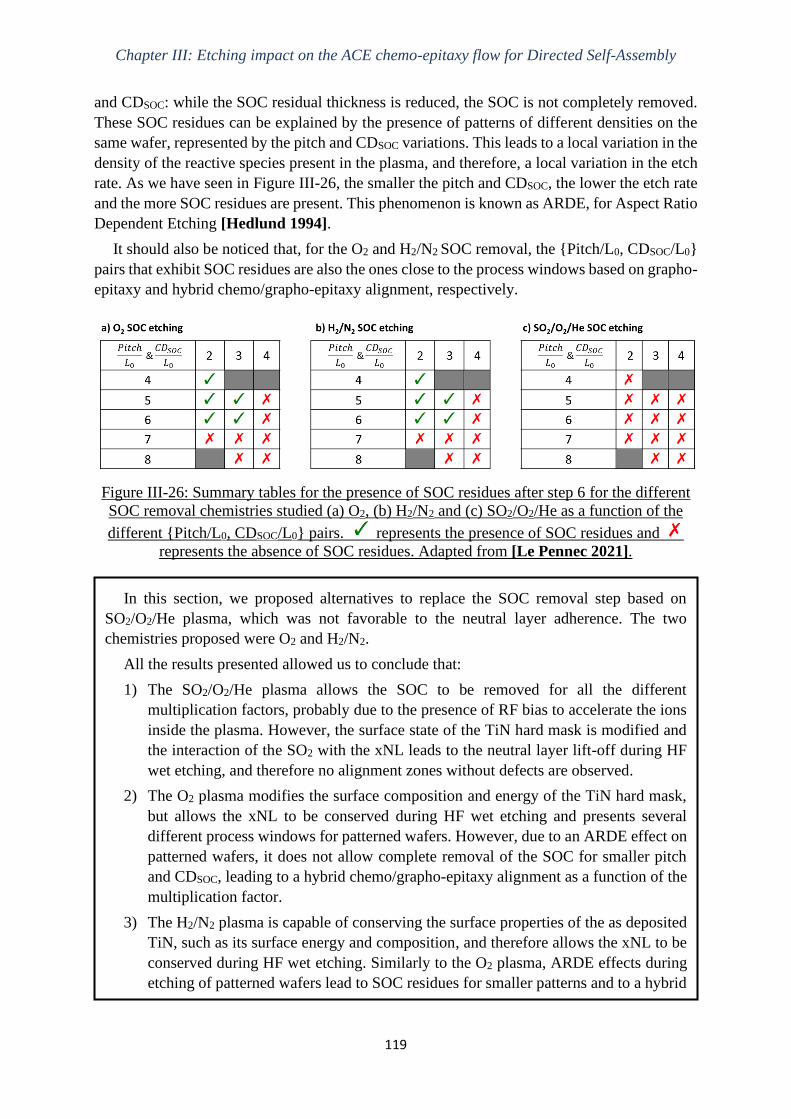
Chapter III: Etching impact on the ACE chemo-epitaxy flow for Directed Self-Assembly
119
and CDSOC: while the SOC residual thickness is reduced, the SOC is not completely removed.
These SOC residues can be explained by the presence of patterns of different densities on the
same wafer, represented by the pitch and CDSOC variations. This leads to a local variation in the
density of the reactive species present in the plasma, and therefore, a local variation in the etch
rate. As we have seen in Figure III-26, the smaller the pitch and CDSOC, the lower the etch rate
and the more SOC residues are present. This phenomenon is known as ARDE, for Aspect Ratio
Dependent Etching [Hedlund 1994].
It should also be noticed that, for the O2 and H2/N2 SOC removal, the {Pitch/L0, CDSOC/L0}
pairs that exhibit SOC residues are also the ones close to the process windows based on grapho-
epitaxy and hybrid chemo/grapho-epitaxy alignment, respectively.
Figure III-26: Summary tables for the presence of SOC residues after step 6 for the different
SOC removal chemistries studied (a) O2, (b) H2/N2 and (c) SO2/O2/He as a function of the
different {Pitch/L0, CDSOC/L0} pairs. represents the presence of SOC residues and
represents the absence of SOC residues. Adapted from [Le Pennec 2021].
In this section, we proposed alternatives to replace the SOC removal step based on
SO2/O2/He plasma, which was not favorable to the neutral layer adherence. The two
chemistries proposed were O2 and H2/N2.
All the results presented allowed us to conclude that:
1) The SO2/O2/He plasma allows the SOC to be removed for all the different
multiplication factors, probably due to the presence of RF bias to accelerate the ions
inside the plasma. However, the surface state of the TiN hard mask is modified and
the interaction of the SO2 with the xNL leads to the neutral layer lift-off during HF
wet etching, and therefore no alignment zones without defects are observed.
2) The O2 plasma modifies the surface composition and energy of the TiN hard mask,
but allows the xNL to be conserved during HF wet etching and presents several
different process windows for patterned wafers. However, due to an ARDE effect on
patterned wafers, it does not allow complete removal of the SOC for smaller pitch
and CDSOC, leading to a hybrid chemo/grapho-epitaxy alignment as a function of the
multiplication factor.
3) The H2/N2 plasma is capable of conserving the surface properties of the as deposited
TiN, such as its surface energy and composition, and therefore allows the xNL to be
conserved during HF wet etching. Similarly to the O2 plasma, ARDE effects during
etching of patterned wafers lead to SOC residues for smaller patterns and to a hybrid

Chapter III: Etching impact on the ACE chemo-epitaxy flow for Directed Self-Assembly
120
III.3.2 Second approach: two-step SOC removal
In order to further optimize the block copolymer’s alignment with the ACE flow, our second
approach consists in a two-step SOC removal. It starts with the SO2/O2/He plasma to completely
remove the SOC layer followed by the O2 or H2/N2 plasma to recover a TiN surface state
compatible with the xNL.
We have followed the same procedure as the previous studies: TiN blanket wafers with a
73-nm SOC layer were etched using the SO2/O2/He plasma, followed by either the O2 plasma
in the same ICP reactor or the H2/N2 in the CCP reactor of the same etching tool. Therefore, in
both cases, no air exposure took place between the first and second steps. Ex-situ XPS analysis
and contact angle measurements were conducted to evaluate the TiN surface properties after
the two-step approach. Furthermore, the xNL was deposited and its thickness was measured
before and after HF wet etching to evaluate its adherence to the TiN surface. And finally the
results when applying the two-step approach to patterned wafers are also evaluated.
III.3.2.1 Effect of the SOC removal two-step approach on the TiN surface
composition
The XPS results for both two-step approaches are presented in Figures III-27(e) and (f). The
results before etching and after etching with each step separately are also included in Figures
III-27(a) to (d) for comparison purposes. For the SO2/O2/He + O2 SOC removal presented in
Figure III-30(f), it should be noticed that about 5% of sulfur is still present after the O2 post-
treatment, corresponding to the SO42- S2p peak at 169.2 eV. Therefore, this two-step approach
with the oxidizing post-treatment has not been able to completely remove the sulfur from the
TiN surface and, from the results presented throughout this chapter, should not be expected to
preserve the neutral layer adherence during HF wet etching. As for the SO2/O2/He + H2/N2 SOC
removal presented in Figure III-27(e), the TiN surface composition after the two-step approach
is quite similar to the one after H2/N2 only, albeit a 4% decrease in the nitrogen percentage,
characteristic of a decrease of the TiN peak, and 4% increase of the oxygen content, due to an
increase of the TiO2 peak. Most importantly, no sulfur is presented in Figure III-27(e).
Therefore, this two-step approach with the reducing post-treatment is capable of completely
removing the sulfur from the TiN surface and should be expected to preserve the neutral layer
adherence during HF wet etching.
chemo/grapho-epitaxy alignment. While this approach presents the best defectivity result
for a single {CDSOC/pitch} pair, with 0 def/100µm² for a lithography pitch of 128 nm, it
presents fewer process windows compared to O2 plasma.

Chapter III: Etching impact on the ACE chemo-epitaxy flow for Directed Self-Assembly
121
Figure III-27: TiN surface composition determined by ex-situ XPS: (a) before etching; (b)
after SO2/O2/He SOC removal; (c) after H2/N2 SOC removal; (d) after O2 SOC removal; (e)
after SO2/O2/He + H2/N2 SOC removal; and (f) after SO2/O2/He + O2 SOC removal. The
results correspond to an incident angle of 23.75°.
III.3.2.2 Contact angle and surface energy measurements
Similarly to the previous sections, the contact angle measurements have also been conducted
to obtain the surface energy of these samples after the two-step SOC removal and the results
are presented in Table III-14. For the SO2/O2/He + O2 SOC removal, the results obtained were
similar to those seen in the previous sections for other oxidative chemistries: a significant
increase of the surface energy and polar component after etching. As for the SO2/O2/He + H2/N2
removal, it is important to notice that the polar component is similar to that of the as deposited
TiN and of the TiN after H2/N2 only, therefore confirming the results obtained from XPS: the
reductive post-treatment is capable of recovering the TiN surface properties even after SO2-
based modification.
Table III-14. TiN surface energy before and after the alternative two-step SOC removal
approaches, calculated by contact angle measurements, as well as its dispersive and polar
components.
Surface energy
γ (mN/m)
Dispersive component
γd (mN/m)
Polar component
γp (mN/m)
As deposited TiN 43.8 37.3 6.5
After SO2/O2/He + H2/N2 53.1 45.2 7.9
After SO2/O2/He + O2 76.9 41.3 35.6

Chapter III: Etching impact on the ACE chemo-epitaxy flow for Directed Self-Assembly
122
III.3.2.3 Effect of the wet spacer removal step on the neutral layer adherence
The neutral layer deposition and HF wet etching have been conducted in order to verify the
correct adherence of the neutral layer over the modified TiN surface after two-step SOC
removal. Table III-15 presents the thickness measurement results for both two-step SOC
removal approaches. As expected based on the XPS results for the SO2/O2/He + O2 SOC
removal, the neutral layer is removed after 60 seconds of HF wet etching. Thus, this approach
is not adequate for the neutral layer adherence. The SO2/O2/He + H2/N2 SOC removal, on the
other hand, presents the same xNL thickness before and after HF wet etching. Therefore, the
reducing post-treatment presents a favorable surface for the neutral layer adherence.
Table III-15. Neutral layer thickness measured by ellipsometry before and after 60 seconds of
HF wet etching when deposited over the TiN surface after the two-step SOC removal using
SO2/O2/He + H2/N2 and SO2/O2/He + O2.
Neutral layer thickness (nm) Before HF (nm) After HF (nm)
After SO2/O2/He + H2/N2 8.0 ± 0.3 8.1 ± 0.3
After SO2/O2/He + O2 8.2 ± 0.3 0.0 ± 0.0
III.3.2.4 Application to patterned wafers using the ACE chemo-epitaxy flow
Finally, the SO2/O2/He + H2/N2 two-step SOC removal has been applied to patterned wafers
following the complete ACE flow presented in Section III.1. Figure III-28 represents the results
obtained for two different multiplication factors after the BCP self-assembly step for the PS-b-
PMMA block copolymer with 32 nm pitch. The PMMA phase has been removed through dry
etching to enhance the contrast and facilitate the image capture. For both MFs, the 1 x 1 µm
top-view SEM images do not present any type of alignment or lift-off defects, which translates
to 0 def/µm².
Figure III-28: 1 x 1 µm top-view SEM images of the PS-b-PMMA block copolymer with
pitch 32 nm aligned by the ACE flow using the SO2/O2/He + H2/N2 two-step SOC removal
approach. (a) corresponds to a multiplication factor of 4 and a lithography pitch of 128 nm,
while (b) corresponds to a multiplication factor of 6 and a lithography pitch of 190 nm.

Chapter III: Etching impact on the ACE chemo-epitaxy flow for Directed Self-Assembly
123
For further evaluation of the DSA alignment results as a function of the SO2/O2/He + H2/N2
two-step SOC removal, a defectivity map was obtained at the DSA step following the same
procedure presented in section III.3.1.4. Figure III-29 presents the defectivity map obtained by
compiling the defectivity results of several 1 x 1 µm CD-SEM images, such as the ones
presented in Figure III-28, taken all over the wafer to cover most of the {CDSOC/pitch} pairs
available, which are represented in the map as a function of the block copolymer’s intrinsic
period L0.
For the defectivity map presented in Figure III-29, we can observe a large number of patterns
presenting an alignment with 0 def/µm² (purple pixels) and at least 14 process windows can be
discerned, which is greater than all the other processes presented previously. It is important to
notice that the PWs are mainly centered around the orange crosses, significant of a
commensurability for which CDSOC = (n - 0.5) L0. Therefore, the ACE integration with a
SO2/O2/He + H2/N2 two-step SOC removal is determined mainly by chemo-epitaxy.
However, for the process windows with (MF = Pitch/L0) ≥ 7, at least 4 of them are located
on the area between the orange crosses and red circles, characteristic of an hybrid
chemo/grapho-epitaxy alignment. A. Le Pennec has proposed a mechanism to explain this
hybrid alignment on higher MF, based on the difference in xNL thickness as a function of the
lithography pitch. According to her observations, the xNL is thinner for larger lithography pitch,
leading to a difference in height between the neutral layer and the guide layer and, therefore, a
hybrid chemo/grapho-epitaxy process determined by both the difference in height and the
difference in chemical affinity of the neutral layer and guiding layer [Le Pennec 2021].
These results allow us to conclude that the various etching steps preceding the deposition of
the neutral layer have a significant impact on the block copolymer’s alignment, as well as the
type of alignment observed (chemo or grapho-epitaxy). Most importantly, the adherence of
xNL is highly influenced by the surface properties of the TiN hard mask.
Figure III-29: Defectivity map obtained for the ACE flow using the SO2/O2/He + H2/N2 two-
step SOC removal approach. The orange cross and red circle symbols represent the theoretical
commensurability values for chemo-epitaxy and grapho-epitaxy, respectively. Adapted from
[Le Pennec 2021].

Chapter III: Etching impact on the ACE chemo-epitaxy flow for Directed Self-Assembly
124
III.4 Conclusions
In this chapter, we began by detailing and characterizing the Arkema-CEA (ACE) chemo-
epitaxy process flow. However, when applying the non-optimized process of reference to
patterned wafers, we realized that different types of defects could be seen in the CD-SEM image
of the block copolymer’s alignment after the DSA step, such as dark spots and BCP alignment
defects.
This led us to study the impact of the different etching steps present on the ACE flow on the
surface properties (composition and surface energy) of the TiN hard mask. The goal was to
understand the origin of the defects and evaluate the hard mask’s capability to align the block
copolymer after the different etching and deposition steps. By studying the effect of the
sequence of etching and deposition steps on the TiN surface and neutral layer adherence using
blanket wafers, we concluded that the dark spots and BCP alignment defects were caused by a
lift-off phenomenon, confirming the inadequacy of the non-optimized flow to align the block
copolymer.
We then investigated the effect of each etching step on the TiN surface. We observed that
all of them induced significant surface energy and composition modifications when compared
to the pristine TiN hard mask. Next, to verify the adherence of the neutral layer to the TiN
surface modified by the different etching steps, the neutral layer thickness was measured before
and after HF wet etching. Ellipsometry measurements showed that the neutral layer is
completely removed for the samples after trilayer etching and SOC removal, which were both
based on SO2/O2/He. This led to the conclusion that the TiN surface after SO2/O2/He plasma
was not favorable to the neutral layer adherence and, as a result, this layer could not resist the
HF wet etching.
Further investigation on the effect of the RF bias and each gas (SO2, O2 and He) separately
showed that, while O2 highly oxidizes the TiN surface and increases its surface energy, it does
not have a negative effect on the neutral layer adherence, thus allowing this layer to resist the
HF wet etching step. The same was concluded for the helium, which does not prevent the
adherence of the neutral layer. The RF Bias power also does not seem to be the most significant
parameter. Indeed, without RF Bias, even though the TiN modified layer is thinner when
In order to further optimize the block copolymer’s alignment with the ACE flow, the
second approach consisted in a two-step SOC removal. It starts with the SO2/O2/He plasma
to completely remove the SOC layer followed by the O2 or H2/N2 plasma to recover a TiN
surface state compatible with the xNL.
The O2 post-treatment after the SO2/O2/He plasma was not able to completely remove
the modified TiO2/TiOxSy/SO42- layer from the TiN surface and, therefore, the neutral layer
was removed during the HF dip.
Therefore, based on the work presented throughout this chapter, the SOC removal
process that exhibited the best alignment was obtained using a SO2/O2/He plasma followed
by a H2/N2 plasma. The combination of both plasmas allows for all of the prerequisites to
be met: the SOC layer is completely removed, the TiN surface properties are conserved, the
xNL adheres to the TiN surface throughout the HF wet etching step, and the ACE process
is determined mainly by chemo-epitaxy.
Chapter III: Etching impact on the ACE chemo-epitaxy flow for Directed Self-Assembly
125
compared to the same process with Bias, the neutral layer is still almost completely removed,
which means the SO2/O2/He plasma etching chemistry was not adapted to the chemo-epitaxy
application. Finally, this led to the conclusion that the SO2 molecule was the main responsible
for this recipe’s inadequacy to the ACE flow.
Once the SO2 was determined to be responsible for the lift-off, our goal was to understand
the interaction mechanisms between the SO2 plasma, the TiN surface, the xNL deposition and
the HF wet etching that led to the lift-off of the neutral layer. Several hypotheses were proposed.
Ultimately, hypothesis #3 was retained as the most probable: SO42− ions interact with the neutral
layer’s cross-linking agent, disrupting its complete cross-linking and allowing the HF to pass
through. The HF then removes the modified TiO2/TiOxSy layer formed on the TiN surface,
which reduces the neutral layer adherence to the TiN hard mask and allows its consequent lift-
off.
The third part of this chapter consisted in proposing two different alternatives for the SOC
removal: replacing the SO2/O2/He plasma or adding a post-treatment step. To replace the
SO2/O2/He, two plasma chemistries were explored: O2 and H2/N2. The results showed that the
O2 etching modifies the surface composition and energy of the TiN hard mask, but allows the
xNL to be conserved during HF wet etching and presents several different process windows for
patterned wafers. However, due to a microloading effect on patterned wafers, it does not allow
complete removal of the SOC for smaller pitch and CDSOC, leading to a hybrid chemo/grapho-
epitaxy alignment as a function of the multiplication factor. The H2/N2 etching, on the other
hand, is capable of conserving the surface properties of the as deposited TiN, such as its surface
energy and composition, and therefore allows the xNL to be conserved during HF wet etching.
Similarly to the O2 etching, microloading effects during etching of patterned wafers lead to
SOC residues for smaller patterns and to a hybrid chemo/grapho-epitaxy alignment. While this
approach presents the best defectivity result for a single {CDSOC/pitch} pair, with 0 def/100µm²
for a lithography pitch of 128 nm, it presents fewer process windows compared to O2 etching.
In order to further optimize the block copolymer’s alignment with the ACE flow, the second
approach consisted in a two-step SOC removal: SO2/O2/He plasma followed by the H2/N2
plasma. The different results led to the conclusion that this approach exhibits the best alignment
results when compared to the other approaches investigated. Indeed, the combination of both
plasmas allows for all of the prerequisites to be met: the SOC layer is completely removed, the
TiN surface properties are conserved, the xNL adheres to the TiN surface throughout the HF
wet etching step, and the ACE process is determined mainly by chemo-epitaxy.

126

127
CHAPTER IV: ETCHING AND PATTERN TRANSFER OF
PURELY ORGANIC HIGH-χ BLOCK
COPOLYMER

Chapter IV: Etching and pattern transfer of purely organic high-χ block copolymer
128
IV. ETCHING AND PATTERN TRANSFER OF PURELY
ORGANIC HIGH-χ BLOCK COPOLYMER
In Chapter I, we have described the different properties of the block copolymers that allow
them to self-assemble into nanostructures with dimensions inferior to 20 nm. We have also seen
that, once the domains have been aligned into long-range order nanostructures, the next
challenge is to obtain a mask from the patterns formed. In order to do so, we must remove one
of the blocks selectively to the other, as represented in Figure IV-1.
During this chapter, the organic high-χ block copolymer system studied is a modified PS-b-
PMMA with a pitch of 18 nm and lamellar morphology, which was developed by Brewer
Science Inc. and Arkema and shall be identified as “high-χ L18” throughout this chapter. The
main goal of this study is to develop a PMMA removal process selective to the PS and adapted
to the 18-nm pitch on 300 mm wafers.
Figure IV-1: Schematics for the flow used in the etching study of the 18-nm pitch high-χ PS-
b-PMMA block copolymer.
Figure IV-1 shows the etching flow for this high-χ PS-b-PMMA. The initial stack consists
of a 10-nm silicon oxide (SiO2) hard mask layer deposited over the silicon substrate. The neutral
layer composed of PS-r-PMMA with a thickness of around 5 nm was deposited over the SiO2
layer in order to self-assemble the modified PS-b-PMMA block copolymer into vertical
lamellae with a thickness of around 16 nm. At this point of the thesis, the ACE chemo-epitaxy
flow was not yet adapted to the 18-nm pitch and, therefore, all studies have been conducted on
free surface wafers with the fingerprint-like morphology.
We estimate that there should be at least 15 nm of PS plus neutral layer left after PMMA
removal to ensure the correct pattern transfer into the SiO2 hard mask, which means that the
high-χ BCP requires a PMMA:PS selectivity of at least 3.5 due to its reduced initial thickness
(around 16 nm). Once a PMMA removal process that fits the desired selectivity criteria has
been identified, the pattern transfer into the SiO2 hard mask shall be used to validate the etching
approach developed.
We have started by studying PS and PMMA homopolymers to characterize the modified
high-χ PS-b-PMMA, as well as the PMMA:PS selectivity for different plasma etching
chemistries. Once the plasma chemistries that achieve good selectivity between PS and PMMA
have been identified, they shall be evaluated on high-χ PS-b-PMMA patterned wafers with
fingerprint-like morphology.
Part of the work presented in this Chapter has been published in the journal Microelectronic
Engineering [Gusmão 2020].

Chapter IV: Etching and pattern transfer of purely organic high-χ block copolymer
129
IV.1 Modified Polystyrene (PS) and Polymethyl methacrylate
(PMMA) homopolymer results
The modifications done to the standard PS-b-PMMA in order to obtain the modified version
with higher χ and smaller pitch were not detailed by Brewer Science Inc. and Arkema for
confidentiality reasons. Therefore, it is important to characterize both materials and compare
them to the standard PS and PMMA. This information should help us understand the etching
mechanisms involved in order to obtain a good PMMA:PS selectivity for this BCP.
For the X-ray photoelectron spectroscopy (XPS) and etch rate results presented throughout
this section, PS and PMMA homopolymer solutions with the modified high-χ chemistry were
spin-coated on 300 mm silicon blanket wafers and then annealed to obtain 50-nm films. The
procedure for obtaining polymer films has been detailed in Chapter II.1.2.
IV.1.1 Characterization of modified PS and PMMA homopolymers
The surface composition of modified PS and PMMA homopolymers, identified as “hPS”
and “hPMMA” respectively, was characterized by XPS. Even though XPS only allows the
analysis of the first 10 nm of the surface of these materials, we can consider that the results
presented in Figure IV-2 represent the bulk of both the PS and PMMA films because they are
homogeneous before etching.
Figure IV-2(a) shows a comparison of the full survey spectra (binding energies between 0
and 750 eV) for the two homopolymers. The first peak detected around 285 eV corresponds to
the carbon C1s peak and is observed for both PMMA and PS. The second peak detected around
533 eV corresponds to the oxygen O1s peak and is only observed for PMMA [Beamson 1992].
It is important to notice that hydrogen cannot be detected by XPS. Therefore, we can conclude
that PS consists only of carbon and hydrogen, while PMMA consists of carbon, oxygen and
hydrogen. These observations correspond to the standard PS and PMMA structures presented
in Figure II-1 of Chapter II.1.1.1.
From Figure IV-2(b), which represents the C1s spectra for both modified PS and PMMA,
we notice that the XPS analysis for the PS presents two peaks: one around 284.8 eV and another
around 291.5 eV. The peak at 284.8 eV is the sum of two contributions: the first at 284.7 eV,
which corresponds to the aliphatic carbon (carbon bonds without an aromatic ring), and the
second at 285 eV, which corresponds to the phenyl compound (C6H5-R). Due to the small
difference in binding energy between both bonds, they cannot be dissociated with the spectral
resolution used. Therefore, these peaks will be represented together as C-C/C=C. The other
peak is observed at 291.5 eV and represents a shake-up peak characteristic of the aromatic
cycle, represented as pi→pi* [Beamson 1992].
As for PMMA, the C1s peaks are as follows: a peak at 285.0 eV represents both the carbon
resulting from the methylene (-CH2) and methyl (-CH3) groups at 284.7 eV and the carbon from
the acrylate compounds (CHCOOH) at 285.5 eV. The sum of both contributions will be
represented as C-C/C=C in Figure IV-2(d), even though the PMMA does not present C=C
double bonds, because it corresponds to the same binding energy value of the C-C/C=C PS
peak. The second peak appears at 286.5 eV and represents the carbon in the methyl ester (C-O)
bonds. The last one, located at 288.8 eV, corresponds to the carbon in the carboxyl group (C=O)
[Beamson 1992].

Chapter IV: Etching and pattern transfer of purely organic high-χ block copolymer
130
The O1s peaks observed in Figure IV-2(c) confirm the observations already made. PS does
not present any O1s peaks, while PMMA presents a first peak at 532.0 eV and the other one at
533.7 eV corresponding to O=C and O-C bonds, respectively [Beamson 1992].
Finally, following the analysis of the various contributions present in PS and PMMA, we
can quantify each of them and thus define the composition of these two polymers. Figure IV-
2(d) shows that the PS is only composed of carbon-carbon and carbon-hydrogen bonds, as
expected by the known formula of the material presented in Figure II-1 of Chapter II.1.1.1.
Regarding the PMMA, we observe a composition of 72.7% carbon and 27.3% oxygen since
hydrogen cannot be detected by XPS. This result is consistent with the values that can be
calculated from the mass of each element and the abbreviated formula of PMMA (C6H5O2)
[Beamson 1992].
Therefore, we can conclude that the modified high-χ PS and PMMA present a composition
similar to that of the standard PS and PMMA.
Figure IV-2: Surface composition of modified PS and PMMA homopolymers obtained by ex-
situ XPS: (a) survey spectra; (b) C1s spectra; (c) O1s spectra; and (d) atomic percentage of
each peak identified on the C1s and O1s spectra. The results correspond to an incident angle
of 23.75°.
IV.1.2 Evaluation of different plasma chemistries for PMMA removal
selectively to the PS
As we have seen in Chapter I.5.1, the main difficulty in the PS-b-PMMA etching is to obtain
high selectivity between PMMA and PS films, since both are organic blocks. The PMMA
removal selectively to PS is usually preferred, since PMMA presents a higher plasma etching

Chapter IV: Etching and pattern transfer of purely organic high-χ block copolymer
131
rate according to the Ohnishi parameter, which is based on the observation that materials
containing a high concentration of C–O and C=O groups exhibit much higher sputter yields
than pure carbon materials [Ohnishi 1983].
The first chemistries developed for the selective PMMA removal regarding the PS were
based on O2. However, this chemistry only achieves a selectivity of around 2.0 on homopolymer
wafers [Liu 2007]. The other disadvantage of the O2 only approach is the lack of dimensional
control, since oxygen leads mainly to an isotropic etching, thus inducing a lateral consumption
of the patterns. In order to increase the PMMA:PS selectivity and improve dimensional control,
O2 was then combined with a chemically inert gas, such as argon (Ar), which does not induce
lateral etching. Ting et al. showed that adding argon to the O2 plasma does not improve
selectivity, which is still around 2.0, but it improves pattern roughness. They also showed that
a PMMA:PS selectivity of around 3.6 can be achieved when argon is used on its own, because
only the bonds resistance to ion bombardment determines the selectivity between the two
materials, thus the PS is consumed very little by this plasma. However, the results obtained on
lamellar patterns show that with a pure Ar plasma, the resulting PS domains have a rough
surface and wider CD than expected. Indeed, the PS seems to deform and occupy the space left
by the PMMA. Therefore, pure Ar does not allow the conservation of the patterns [Ting 2008].
Finally, based on these results, Chan et al. developed a cyclic Ar + Ar/O2 approach, leading to
a selectivity of around 3.0 [Chan 2014]. Despite these improvements, O2-based chemistries are
limited in terms of PMMA:PS selectivity and dimensional control.
One of the alternatives to O2 is the use of carbon monoxide (CO), in which oxygen is
responsible for etching while carbon allows for better selectivity between both blocks. Sarrazin
et al. evaluated the behavior of CO etching on PS and PMMA homopolymers. They observed
that while PMMA is etched, a deposit is created on the PS. However, after 10 seconds of CO
plasma, an etch saturation is verified for the PMMA. In order to avoid an etch stop and
completely remove the PMMA, a small amount of hydrogen (H2) is added to control the
polymerization, thus allowing a 50-nm PMMA film to be fully etched with a selectivity around
12.0. However, when applying this chemistry to PMMA cylinders, this selectivity decreases to
around 3.5 [Sarrazin 2016]. To improve the selectivity, Sarrazin et al. developed a cyclic
approach based on CO + CO/H2 combining the higher selectivity of CO with the polymerization
control of CO/H2 [Sarrazin 2018]. The CO + CO/H2 plasma cycles were shown to be suitable
for the cylindrical application, with infinite PMMA:PS selectivity, but present limitations for
lamellar application: higher PS consumption due to a higher amount of oxygen (coming from
PMMA) released during etching leads to lower selectivity (around 6.0) [Sarrazin 2017].
Therefore, an oxygen-free chemistry based on CH4/N2 was developed by Sarrazin et al. to
obtain infinite selectivity with lamellar PS-b-PMMA with a 38-nm pitch [Sarrazin 2019].
This section shall present an evaluation of the etch rate of different plasma etching
chemistries applied to modified PS and PMMA homopolymers. The goal is to identify the
chemistries that might be interesting for the 18-nm pitch high-χ PS-b-PMMA, namely regarding
the PMMA:PS selectivity. The plasma parameters for the different chemistries tested are
presented in Table IV-1. All of the experiments for this section were performed in the 300 mm
Kiyo FX® ICP reactor from LamResearch®, which was already presented in Chapter II.2.1.2.
Table IV-2 presents the PS and PMMA homopolymer etch rates, as well as the
corresponding PMMA:PS selectivity, calculated by applying the different etching chemistries
presented in Table IV-1 for 10 seconds.

Chapter IV: Etching and pattern transfer of purely organic high-χ block copolymer
132
The first chemistry evaluated was a CH3F/Ar/SO2 plasma proposed as a Best-Known Method
(BKM) by LamResearch®. This recipe presents a RF bias pulsing mode, which consists of
alternating two cycles during a single step, according to the specified pulsing frequency: one
cycle of RF Bias ON and one cycle of RF Bias OFF. As we have seen in Chapter II.2.1.2, the
RF Bias in an ICP reactor is the parameter that allows us to have a strong ion bombardment and
thus increase the anisotropic aspect of the etching. The pulsing mode usually allows for better
profile and selectivity, since it increases the uniformity of the passivation layer [Agarwal
2009]. Indeed, during RF bias OFF, the passivation layer is deposited on the sidewalls without
the effect of ion bombardment, which may consume the mask through sputtering and also lead
to a faceted profile. For this recipe, the RF bias pulsing conditions were: duty cycle, which
corresponds to the percentage of ON time, at 31% and pulsing frequency at 300 Hz. These
parameters shall not be varied during our studies. The CH3F/Ar/SO2 plasma presented a
PMMA:PS selectivity of 3.5 on blanket homopolymers.
The second plasma evaluated was an Ar/O2 plasma, which has been vastly studied in the
literature and, for the parameters chosen, presented a selectivity of 3.4, superior to the results
shown in the literature, but still inferior to the other plasma etching chemistries presented in
Table IV-2. And the third one was the oxygen-free etching based on CH4/N2, which presents
infinite PMMA:PS selectivity since no PS was consumed.
Table IV-1: Plasma parameters for the different chemistries tested on modified PS and PMMA
homopolymers.
Chemistry Pressure (mTorr) Power (W) Bias (V) Flow (sccm)
CH3F/Ar/SO2 10 250 -650
(pulsed) 30/200/150
Ar/O2 10 220 -100
(continuous) 50/5
CH4/N2 10 500 -200
(continuous) 50/50
Table IV-2: Modified PS and PMMA homopolymer etch rates, as well as the corresponding
PMMA:PS selectivity, calculated for the different etching chemistries. Etching duration was 10
seconds.
Chemistry Etch rate modified
hPS (nm/s)
Etch rate modified
hPMMA (nm/s)
hPMMA:hPS
selectivity
CH3F/Ar/SO2 1.3 4.6 3.5
Ar/O2 0.8 2.7 3.4
CH4/N2 0.0 1.1 ∞

Chapter IV: Etching and pattern transfer of purely organic high-χ block copolymer
133
Based on these preliminary results, the CH3F/Ar/SO2 and CH4/N2 plasma chemistries, which
fulfill our requirement by presenting a PMMA:PS selectivity ≥ 3.5, have been selected for
testing on the modified high-χ PS-b-PMMA and the results shall be presented throughout the
next section.
IV.2 Application to high-χ PS-b-PMMA films with lamellar
morphology
In this section, we shall apply the selected plasma chemistries from the previous section to
the high-χ modified PS-b-PMMA with two different pitch: the 18-nm pitch, also known as
“high-χ L18”, and a 32-nm pitch modified PS-b-PMMA, which shall be referred to as “high-χ
L32”. The high-χ L32 presents the same modified chemistry of the high-χ L18, but with a larger
pitch (32 nm) and initial thickness (36 nm).
All high-χ PS-b-PMMA experiments were conducted on 300 mm silicon wafers with a 10-
nm SiO2 layer. A thin neutral layer composed of PS-r-PMMA random copolymer is spin-coated
on the substrate before the BCP deposition in order to neutralize the surface. Then, the BCP
solution is spin-coated and annealed to form the vertical lamellae morphology. The L18 BCP
presents the dimensions shown in Figure IV-1(1). For the high-χ L32, the neutral and BCP layer
thicknesses are around 8 and 36 nm, respectively.
IV.2.1 Impact of high-χ modified PS-b-PMMA chemistry for same pitch and
plasma chemistry
In section IV.1.1, the XPS analysis of the modified PS and PMMA have shown no significant
difference in composition between standard and modified PS-b-PMMA. In this section, our
goal is to verify if the high-χ modified PS-b-PMMA chemistry has no impact on the etching of
this BCP when applied to patterned wafers. In order to do so, the same PMMA removal process
shall be applied to two block copolymers with same pitch and initial thickness: the high-χ L32
BCP and a standard PS-b-PMMA, also with 32-nm pitch, which we have already used
throughout chapter III. The same neutral layer (NL) is used for both copolymers and the BCP’s
initial thickness is also the same (36 nm), leading to a BCP + NL initial thickness of 44 nm.
The top-view and cross-section SEM images of the high-χ L32 and standard L32 PS-b-PMMA
In this section, we have characterized the composition of the modified PS and PMMA
homopolymers that compose the high-χ modified PS-b-PMMA block copolymer. We have
concluded that the modified PS-b-PMMA presents a composition similar to that of standard
PS-b-PMMA: indeed, modified PS is composed of carbon and hydrogen with an aromatic
ring, while modified PMMA is an aliphatic compound composed of carbon, hydrogen and
oxygen.
We have also seen the evolution of the PMMA removal through plasma etching, which
has seen an improvement on PMMA:PS selectivity throughout the years thanks to different
gases used. Then, we selected some of these well-known plasma chemistries and we
evaluated their etch rate, and consequent selectivity, on modified PS and PMMA
homopolymers, therefore selecting two different chemistries that fulfill our selectivity
requirement: CH3F/Ar/SO2 and CH4/N2.

Chapter IV: Etching and pattern transfer of purely organic high-χ block copolymer
134
block copolymer after PMMA removal using the CH3F/Ar/SO2 plasma for 12 seconds are
presented in Figure IV-3.
From Figure IV-3(a), we observe that after PMMA removal during 12 seconds, the PMMA
has been completely removed and around 3.4 nm of neutral layer remain, which translates to a
total PMMA + NL consumed thickness of 40.6 nm. Moreover, the PS + NL remaining thickness
is around 18.8 nm, meaning 25.2 nm of PS have been consumed. Therefore, the PMMA:PS
selectivity for the high-χ L32, determined by the ratio between consumed PMMA+NL (40.6
nm) and consumed PS (25.2 nm) is approximately 1.6.
The same calculation can be done for the standard L32, based on the results of Figure IV-
3(b): after PMMA removal for the same duration, the PMMA has also been completely
removed and around 2.7 nm of neutral layer remain, which translates to a PMMA + NL
consumed thickness of 41.3 nm. Moreover, the PS + NL remaining thickness is around 18.5
nm, meaning 25.5 nm of PS have been consumed. Therefore, the PMMA:PS selectivity for the
standard L32 is approximately 1.6, similar to the high-χ L32.
Furthermore, the CD measurements in Figures IV-3(a) and (b) are quite similar for both
block copolymers and the line patterns present the same profile, with a difference of
approximately 5.5 nm between the top CD (~ 9 nm) and the bottom CD (~14.5 nm).
Figure IV-3: Top-view and cross-section SEM images of the (a) high-χ L32 and (b) standard
L32 PS-b-PMMA block copolymer after PMMA removal using the CH3F/Ar/SO2 plasma for
12 seconds.

Chapter IV: Etching and pattern transfer of purely organic high-χ block copolymer
135
Therefore, we can conclude that, for the same pitch and initial thickness, the high-χ modified
PS-b-PMMA chemistry does not present a significant impact on the PMMA plasma etching
when compared to the standard PS-b-PMMA block copolymer.
It should also be noticed that the selectivity on free surface pattern wafers is lower compared
to that of the homopolymer wafers presented in Table IV-2, which has already been observed
in the literature and indicates that new etching mechanisms come into place when the two block
copolymer’s phases interact.
IV.2.2 Impact of pitch and film thickness on the etching of high-χ modified
PS-b-PMMA
Now that we have shown that the high-χ modified PS-b-PMMA chemistry does not present
a significant impact on the PMMA etching, our goal is to verify the impact of the reduced pitch
and film thickness of the high-χ PS-b-PMMA on the PMMA removal. In order to do so, we
shall apply the CH3F/Ar/SO2 and CH4/N2 plasma chemistries, selected in section IV.1.2 for
their good PMMA:PS selectivity, on the high-χ PS-b-PMMA with two different pitch and initial
thickness: L18 and L32. As we have seen before, the high-χ L18 presents a pitch of 18 nm and
initial thickness of 16 nm, leading to a total BCP+NL initial thickness of 21 nm. As for the
high-χ L32, it presents a pitch of 32 nm and a total BCP+NL initial thickness of 44 nm.
For the etching of the high-χ PS-b-PMMA, we have estimated that there should remain at
least 15 nm of PS plus neutral layer after PMMA removal to ensure the correct pattern transfer
into the SiO2 hard mask. For the high-χ L32, this means a selectivity superior to 1.5. However,
for the high-χ L18, due to its reduced initial thickness of 21 nm, the desired selectivity is around
3.5. Therefore, the BCP with smaller pitch requires higher selectivity when compared to the
same BCP with larger pitch. This increases the importance of developing a plasma etching
process that allows for high selectivity between both phases of the high-χ BCP.
Figure IV-3(a) already presented the results for high-χ L32 after CH3F/Ar/SO2, which leads
to a PMMA:PS selectivity of 1.6 and a PS+NL remaining thickness of 18.8 nm after 12 seconds
of etching. Figure IV-4(a) presents the SEM images for the high-χ L18 after CH3F/Ar/SO2 for
6 seconds. In this case, the PMMA has almost been completely removed and around 5.4 nm of
PMMA + neutral layer remain, which translates to a total PMMA + NL consumed thickness of
15.6 nm. Moreover, the PS + NL remaining thickness is around 11 nm, meaning 10 nm of PS
have been consumed. Therefore, the PMMA:PS selectivity for the high-χ L18, determined by
the ratio between consumed PMMA+NL (15.6 nm) and consumed PS (10 nm) is approximately
1.6, similar to the selectivity obtained for the high-χ L32 using the same chemistry.
As for the oxygen-free PMMA removal based on CH4/N2, Figure IV-4(b) shows that, for the
high-χ L32, the PMMA and its subjacent neutral layer have both been completely removed after
60 seconds of etching. This translates to a total PMMA + NL consumed thickness of 44 nm.
Moreover, the PS + NL remaining thickness is around 30.4 nm, meaning 13.6 nm of PS have
been consumed. Therefore, the PMMA:PS selectivity for the high-χ L32 with the oxygen-free
chemistry is approximately 3.2. Finally, for the same chemistry applied to high-χ L18, Figure
IV-4(c) shows that 13.3 nm of PMMA and 5.1 nm of PS have been consumed after 30 seconds
of etching, leading to a PMMA:PS selectivity of 2.6, which is slightly inferior when compared
to the L32.

Chapter IV: Etching and pattern transfer of purely organic high-χ block copolymer
136
Figure IV-4: Top-view and cross-section SEM images of the (a, c) high-χ L18 and (b) high-χ
L32 PS-b-PMMA block copolymers after PMMA removal using two different plasma
chemistries: (a) CH3F/Ar/SO2 and (b, c) CH4/N2. It should be noticed that the cross-section
SEM measurements are approximations, due to the tool’s lower precision when using higher
magnification.
Many conclusions can be drawn based on these results. It is important to notice that, once
again, for both plasma chemistries investigated, the selectivity on free surface pattern wafers is
lower compared to that of the homopolymer wafers presented in Table IV-2. For example, the
CH4/N2 selectivity decreases from infinite on homopolymers to around 3.0 on free surface

Chapter IV: Etching and pattern transfer of purely organic high-χ block copolymer
137
wafers, confirming that new etching mechanisms come into place when the two block
copolymer’s phases interact. As we have seen on the XPS analysis of the PMMA
homopolymers presented in section IV.1.1, PMMA presents C-O and C=O bonds. During
plasma etching of the PS-b-PMMA BCP, these C-O simple and double bonds are broken,
forming volatile oxygen-containing by-products, which probably interact with the PS phase and
induce its consumption.
It should also be noticed that, for the same CH4/N2 etching, the high-χ L18 BCP presents
lower selectivity compared to the high-χ L32. This might be due to the fact that the etching time
is shorter for the BCP with smaller thickness, and thus indicates a dependence of the PMMA:PS
selectivity on the etching duration for this chemistry. However, it is important to highlight that
the cross-section SEM measurements are approximations, due to the tool’s lower precision
when using higher magnification. Therefore, we cannot determine the degree of significance of
the difference in selectivity between both pitch.
In order to better evaluate the results for the high-χ L18, we proceeded to the pattern transfer
into the SiO2 hard mask after removing the PMMA with the two different plasma chemistries.
For the SiO2 etching, we used a CHF3/CF4 plasma for 8 seconds with the following parameters:
50/50 sccm, pressure 4 mTorr, RF power 625 W and RF bias 110 V. The results can be found
in Figure IV-5.
Regarding the CH3F/Ar/SO2 etching, we have seen that it leads to a PMMA:PS selectivity
of 1.6. However, while for the high-χ L32, the low 1.6 selectivity is still enough to ensure the
pattern transfer into the SiO2 layer, the same cannot be said for the high-χ L18. Indeed, with a
selectivity of 1.6, Figure IV-5(a) shows that the same chemistry cannot allow the pattern
transfer when applied to the BCP with 18-nm pitch.
Figure IV-5: Top-view SEM images of the high-χ L18 PS-b-PMMA block copolymer after
pattern transfer into the SiO2 hard mask. The PMMA removal was conducted using two
different plasma chemistries: (a) CH3F/Ar/SO2, and (b) CH4/N2.
As for the CH4/N2 etching, the top-view image in Figure IV-4(c) highlights the formation of
bridges between the PS lines for the high-χ L18, which were not present on the high-χ L32 PS-
b-PMMA shown in Figure IV-4(b). Figure IV-5(b) shows that these bridges prevent the
complete pattern transfer of the PS lines into the SiO2 hard mask. The origin of these bridges
will be further explored in section IV.3.3.

Chapter IV: Etching and pattern transfer of purely organic high-χ block copolymer
138
IV.3 Alternatives for the etching of high-χ PS-b-PMMA films with
18-nm pitch
We have seen in the previous section that, for the high-χ L18 BCP, two main types of
difficulties can be identified: (1) not enough PS budget remaining for pattern transfer and (2)
formation of bridges between the PS lines. The first one is quite evident for highly reactive
chemistries, such as CH3F/Ar/SO2 and Ar/O2 (not represented), that present lower PMMA:PS
selectivity due to the reactivity between oxygen and both organic blocks of the high-χ L18 BCP.
The second one is observed for highly passivating chemistries, such as CH4/N2 and CO/H2 (not
represented), whose selectivity mechanism is mostly based on the deposition of carbon-based
passivating layers over the PS [Sarrazin 2017].
This next section shall present different approaches explored throughout this PhD thesis with
the goal of increasing the PMMA:PS selectivity for the high-χ L18 PS-b-PMMA in order to
validate the pattern transfer into the SiO2 and Si subjacent layers, while also avoiding the
formation of defects, such as bridges.
IV.3.1 First approach: argon-based PMMA removal
The first approach that shall be presented focuses on optimizing the BKM recipe, based on
CH3F/Ar/SO2, which presents low selectivity (around 1.6) for the high-χ L18, but no bridge
formation after PMMA removal. First, a process window for this recipe will be determined by
varying some plasma parameters, such as the RF bias and the gas flow. Then, the impact of
increasing the block copolymer thickness will be evaluated. Finally, a cyclic approach with
argon-based steps shall be explored.
IV.3.1.1 Process window for high-χ L18 with argon-based PMMA removal
For this study, one of the main challenges is to characterize the high-χ L18 block copolymer
after the PMMA removal step, namely due to the small dimensions of the copolymer (pitch and
In this section, we have characterized the impact of the modified chemistry, pitch and
initial thickness on the etching of the high-χ modified PS-b-PMMA.
When comparing a modified and a standard PS-b-PMMA BCP with the same pitch and
initial thickness, we conclude that, for the same plasma etching chemistry, the high-χ
modified PS-b-PMMA chemistry does not present a significant impact on the PMMA
plasma etching when compared to the standard PS-b-PMMA block copolymer.
However, when comparing the high-χ modified PS-b-PMMA with two different pitch
(18 and 32 nm) and two different initial thickness (16 and 36 nm, respectively), for the high-
χ L18 BCP, the same etching chemistries that were validated for larger pitch (32 nm) present
different problems that prevent pattern transfer into the SiO2 hard mask for the smaller BCP.
When using CH3F/Ar/SO2 plasma, there is probably not enough PS budget remaining for
L18 pattern transfer and, when using the CH4/N2 plasma, bridges are formed between the
PS lines, preventing L18 pattern transfer.
Therefore, we can conclude that the main high-χ L18 PS-b-PMMA plasma etching
difficulties come from its small dimensions, namely the pitch and initial thickness.

Chapter IV: Etching and pattern transfer of purely organic high-χ block copolymer
139
remaining PS thickness) coupled with the charging effects typical of polymeric materials during
cross-section SEM observations. For example, when observing the top-view SEM images after
PMMA removal using the CH3F/Ar/SO2 plasma for 6 seconds, which are presented in Figure
IV-4(a), it may seem as though we have succeeded in completely removing the PMMA.
However, when we proceed to the pattern transfer into the silicon oxide, presented in Figure
IV-5(a), we observe that the lines pattern is not conserved. Indeed, these images indicate that
the pattern transfer is not complete, which means the PMMA removal step’s duration was not
enough.
We then started by varying the etch time of the CH3F/Ar/SO2 plasma while conserving the
other parameters presented in Table IV-1. The SEM images are not presented here because, for
shorter durations (t = 5 seconds), the results are similar to the ones observed in Figure IV-
4(a), while for longer durations (t = 7 seconds) the lines pattern is no longer discernible, which
means the PS has probably been completely consumed and there is no more budget for pattern
transfer. These results indicate that the CH3F/Ar/SO2 plasma presents a very narrow process
window, mostly due to the high PMMA and PS etch rates when compared to the other
chemistries evaluated (Table IV-2). A narrow process window is undesired for manufacturing
processes in a microelectronics fab, since the smallest variation in the process can lead to very
different results.
Therefore, in order to reduce the etch rate of both blocks and obtain a larger process window,
we have decided to reduce the RF bias voltage of the recipe, which was set at 325V instead of
the original 650V. Indeed, the RF bias, also known as self-bias voltage, is the main responsible
for the ion acceleration inside the plasma reactor chamber. Since the argon ions – which are
inert and do not react with the BCP blocks – are accelerated by the self-bias voltage and thus
participate on the physical sputtering of the BCP, the RF bias voltage is one of the parameters
that influence the etch rate. To verify the reduction of the etch rate with the lower RF bias,
modified PS and PMMA homopolymer thickness was measured before and after etching with
CH3F/Ar/SO2 325V for 10 seconds. The etch rates for PS and PMMA were calculated at 0.7
nm/s and 2.3 nm/s, respectively, which means the etch rate for both materials is reduced by half
with the lower bias when compared to the original values for 650V presented in Table IV-2.
The results for the CH3F/Ar/SO2 plasma with reduced bias are presented in Figure IV-6.
Figures IV-6(a, b, c) present the top-view images after PMMA removal for different etching
durations (t between 11 and 17 seconds), while Figures IV-6(d, e, f) present the SEM images
after pattern transfer into the SiO2 in order to verify whether the PMMA has been completely
removed. Based on the top-view SEM images after SiO2 etching, we can observe that, for the
PMMA removal for 11 and 14 seconds, the etch duration was not enough to ensure the complete
removal of the PMMA and therefore the correct pattern transfer, leading to wiggling and
eventual pattern collapse. On the other hand, for the PMMA removal during 17 seconds, there
was not enough PS budget remaining for pattern transfer and the lines pattern was no longer
discernible. These results indicate that the CH3F/Ar/SO2 process window is still very narrow
even with the lower bias.

Chapter IV: Etching and pattern transfer of purely organic high-χ block copolymer
140
Figure IV-6: Top-view SEM images of the high-χ L18 block copolymer (a, b, c) after PMMA
removal using CH3F/Ar/SO2 with reduced bias and (d, e, f) after pattern transfer into the SiO2
hard mask using CHF3/CF4 plasma for 8s. The PMMA removal duration was varied and is
indicated on the left by t: (a, d) 11s; (b, e) 14s; and (c, f) 17s.
Since the CH3F/Ar/SO2 recipe presents some carbon passivation in the form of CH3F, we
then tried removing the CH3F from the recipe to verify if it was blocking the PMMA removal
by depositing a fluorocarbon (CxFy) compound on the PS sidewalls. The results are not
represented because they were similar to the ones obtained in Figure IV-6. For an etch duration
of 14 seconds, the etch duration was not enough to ensure the correct pattern transfer, leading
to pattern collapse, while for the PMMA removal during 17 seconds, there was not enough PS
budget remaining for pattern transfer.
These results led us to conclude that the process window for the CH3F/Ar/SO2 plasma is
very narrow due to the small dimensions – pitch and thickness – of the high-χ L18 BCP film.
In order to overcome the dimensional limitation and therefore increase the available PS
budget after etching, we tried increasing the initial thickness of the high-χ L18 PS-b-PMMA
film to 35 nm. However, Figure IV-7 shows that some pattern wiggling is observed after
PMMA removal using the CH3F/Ar/SO2 plasma with the same parameters from Table IV-1.
This is probably due to the high aspect ratio of the lines, which is superior to 2.0 after PMMA
removal. Therefore, we can conclude that, while increasing the initial thickness could be
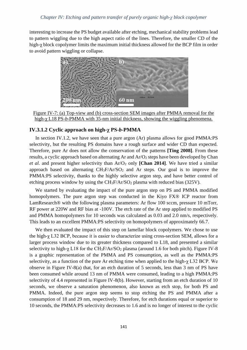
Chapter IV: Etching and pattern transfer of purely organic high-χ block copolymer
141
interesting to increase the PS budget available after etching, mechanical stability problems lead
to pattern wiggling due to the high aspect ratio of the lines. Therefore, the smaller CD of the
high-χ block copolymer limits the maximum initial thickness allowed for the BCP film in order
to avoid pattern wiggling or collapse.
Figure IV-7: (a) Top-view and (b) cross-section SEM images after PMMA removal for the
high-χ L18 PS-b-PMMA with 35-nm initial thickness, showing the wiggling phenomena.
IV.3.1.2 Cyclic approach on high-χ PS-b-PMMA
In section IV.1.2, we have seen that a pure argon (Ar) plasma allows for good PMMA:PS
selectivity, but the resulting PS domains have a rough surface and wider CD than expected.
Therefore, pure Ar does not allow the conservation of the patterns [Ting 2008]. From these
results, a cyclic approach based on alternating Ar and Ar/O2 steps have been developed by Chan
et al. and present higher selectivity than Ar/O2 only [Chan 2014]. We have tried a similar
approach based on alternating CH3F/Ar/SO2 and Ar steps. Our goal is to improve the
PMMA:PS selectivity, thanks to the highly selective argon step, and have better control of
etching process window by using the CH3F/Ar/SO2 plasma with reduced bias (325V).
We started by evaluating the impact of the pure argon step on PS and PMMA modified
homopolymers. The pure argon step was conducted in the Kiyo FX® ICP reactor from
LamResearch® with the following plasma parameters: Ar flow 100 sccm, pressure 10 mTorr,
RF power at 220W and RF bias at -100V. The etch rate of the Ar step applied to modified PS
and PMMA homopolymers for 10 seconds was calculated as 0.03 and 2.0 nm/s, respectively.
This leads to an excellent PMMA:PS selectivity on homopolymers of approximately 66.7.
We then evaluated the impact of this step on lamellar block copolymers. We chose to use
the high-χ L32 BCP, because it is easier to characterize using cross-section SEM, allows for a
larger process window due to its greater thickness compared to L18, and presented a similar
selectivity to high-χ L18 for the CH3F/Ar/SO2 plasma (around 1.6 for both pitch). Figure IV-8
is a graphic representation of the PMMA and PS consumption, as well as the PMMA:PS
selectivity, as a function of the pure Ar etching time when applied to the high-χ L32 BCP. We
observe in Figure IV-8(a) that, for an etch duration of 5 seconds, less than 3 nm of PS have
been consumed while around 13 nm of PMMA were consumed, leading to a high PMMA:PS
selectivity of 4.4 represented in Figure IV-8(b). However, starting from an etch duration of 10
seconds, we observe a saturation phenomenon, also known as etch stop, for both PS and
PMMA. Indeed, the pure argon step seems to stop etching the PS and PMMA after a
consumption of 18 and 29 nm, respectively. Therefore, for etch durations equal or superior to
10 seconds, the PMMA:PS selectivity decreases to 1.6 and is no longer of interest to the cyclic

Chapter IV: Etching and pattern transfer of purely organic high-χ block copolymer
142
application. We have thus selected the duration of the argon step for the cyclic approach as 5
seconds, since it presents higher PMMA:PS selectivity and no etch stop on lamellar high-χ L32.
Figure IV-8: (a) PS and PMMA consumption and (b) PMMA:PS selectivity as a function of
the argon etching time when applied to the high-χ L32 BCP.
Figure IV-9 presents the top-view and cross-section SEM images after the cyclic
CH3F/Ar/SO2 + Ar approach was applied to the high-χ L32 BCP for three complete cycles. The
CH3F/Ar/SO2 325V step duration was also set at 5 seconds to minimize the PS consumption.
The results for the complete PMMA removal using only the CH3F/Ar/SO2 plasma with reduced
bias during 25 seconds were also presented for comparison purposes. Figure IV-9(4) shows that
the PMMA has been completely removed after 25 seconds of etching with the CH3F/Ar/SO2
plasma and around 2.4 nm of neutral layer remain. This translates to a total PMMA + NL
consumed thickness of 41.6 nm. Moreover, the PS + NL remaining thickness is around 15.8
nm, meaning 29.2 nm of PS have been consumed. Therefore, the PMMA:PS selectivity for the
high-χ L32 with the non-cyclic approach is approximately 1.5. As for the cyclic CH3F/Ar/SO2
+ Ar approach, Figure IV-9(b) shows that approximately 40.3 nm of PMMA and 27.6 nm of
PS have been consumed after 3 complete cycles – which corresponds to a total of 30 seconds
of etching –, leading to a PMMA:PS selectivity of 1.5, which is similar to the one calculated
for the non-cyclic approach. Therefore, the cyclic approach based on alternating CH3F/Ar/SO2
and Ar steps does not present an improvement to the PMMA:PS selectivity.

Chapter IV: Etching and pattern transfer of purely organic high-χ block copolymer
143
Figure IV-9: Top-view and cross-section SEM images of the high-χ L32 PS-b-PMMA after
PMMA removal using: (a) CH3F/Ar/SO2 with reduced bias for 25 seconds and (b) 3 cycles of
alternating CH3F/Ar/SO2 and Ar steps for 5 seconds each.
These results can be explained by the analysis of the extreme surface composition of the
modified PS and PMMA homopolymers after etching with the CH3F/Ar/SO2 plasma, obtained
through XPS with an incident angle of 76.25°, which analyzes approximately the first 3 nm of
the surface. The etching time was set at 10 seconds to better evaluate the changes in surface
composition of the modified PS and PMMA. When comparing the modified PS before etching
presented in Figure IV-10(a) with the PS after etching presented in Figure IV-10(b), we observe
that after etching the shake-up pi→pi* peak disappears, which is characteristic of PS etching.
Furthermore, C=O and C-O bonds represent around 67% of the final extreme surface
composition after etching. Given the significant percentage of oxygen after etching, we may
assume that it comes from both the oxygen present in the CH3F/Ar/SO2 plasma and from the air
exposure between the etching and XPS tools. C-F bonds are also identified after etching, but
cannot be differentiated from the C=O bonds due to the spectral resolution (C=O peak at 288.8
eV and C-F peak at 289.5 eV), hence being represented as “C=O, C-F” [Worley 1986]. Finally,
around 12% of sulfur is identified after etching, represented by a S2p3/2 peak at 164.4 eV, which
may correspond to sulfur bound to the aromatic ring and is represented as S(C6H5) [Riga 1978].
As for the modified PMMA after etching with CH3F/Ar/SO2 plasma, presented in Figure IV-
10(d), we observe that the extreme surface composition is quite similar to that of the PS after

Chapter IV: Etching and pattern transfer of purely organic high-χ block copolymer
144
etching, except for the presence of sulfur, which is not observed for PMMA. The absence of
sulfur is compensated by a 7% increase in the C-C bonds percentage and a slight increase
(around 1 or 2%) for the other bonds. Therefore, the similar surface composition between PS
and PMMA after etching with CH3F/Ar/SO2 could explain why adding an argon step does not
improve the selectivity. Thus, this approach is not appropriate to improve the PMMA:PS
selectivity for the high-χ PS-b-PMMA.
Figure IV-10: Surface composition of modified (a, b) PS and (c, d) PMMA homopolymers
obtained by ex-situ XPS: (a, c) before and (b, d) after etching with CH3F/Ar/SO2 for 10
seconds. The results correspond to an incident angle of 76.25°.
In this section, we have tried to optimize the PMMA:PS selectivity for the CH3F/Ar/SO2
plasma, which presents low selectivity (around 1.6) for the high-χ L18, but no bridge
formation. We observed that the CH3F/Ar/SO2 plasma presents a very narrow process
window regarding the etch duration. Indeed, the etch duration was either not enough to
completely remove the PMMA and neutral layer, and therefore the pattern transfer into the
SiO2 hard mask was not correct; or the etch duration was long enough to remove the PMMA
and neutral layer, but there was not enough PS budget remaining for pattern transfer and the
lines pattern was no longer discernible. Reducing the RF bias to decrease the etch rate did
not improve the results. Thus, we concluded that the process window for the CH3F/Ar/SO2
plasma was very narrow due to the small dimensions – pitch and thickness – of the high-χ
L18 BCP film.
In order to overcome the dimensional limitation and therefore increase the available PS
budget after etching, we tried increasing the initial thickness of the high-χ L18 film.
However, mechanical stability problems led to pattern wiggling due to the high aspect ratio
of the lines. Therefore, the smaller CD of the high-χ block copolymer limits the maximum
initial thickness allowed for the BCP film in order to avoid pattern wiggling or collapse.

Chapter IV: Etching and pattern transfer of purely organic high-χ block copolymer
145
IV.3.2 Second approach: UV exposure followed by plasma etching
The use of UV exposure before wet removal is known to improve the selectivity between
PMMA and PS. Indeed, UV radiation causes the degradation of the covalent bond between PS
and PMMA and of the PMMA block through PMMA chain scissions. Moreover, it can also
strengthen the PS bonds and thus reduce their solubility [Thurn-Albrecht 2000] [Gharbi
2015].
Thus, our second approach is based on an UV exposure followed by plasma etching. The
goal is to break the PMMA chains and harden the PS block before plasma removal of the
remaining PMMA and of the neutral layer. This should allow us to obtain higher PMMA:PS
selectivity and also avoid wiggling and pattern collapse, since the PS mechanical stability would
be improved.
IV.3.2.1 Effect of UV exposure on modified PS and PMMA homopolymers
We started by evaluating the impact of UV exposure on modified PS and PMMA
homopolymers. The UV exposure was conducted on the 300 mm SOKUDO DUO tool with a
wavelength of 172 nm. Two different doses were evaluated: 30 and 150 mJ/cm².
Table IV-3 presents the modified PS and PMMA homopolymer thickness reduction (e)
determined by ellipsometry after UV exposure for the two different doses. For both doses, there
is almost no change in PS thickness. As for the PMMA, Table IV-3 shows that the higher the
dose the higher the PMMA thickness reduction after UV exposure, which corresponds to
approximately 5.7 nm for an UV dose of 30 mJ/cm² and a significant 17-nm shrink for a higher
UV dose of 150 mJ/cm².
We then measured the PS and PMMA consumption after etching with CH3F/Ar/SO2 for 8
seconds, with and without UV exposure. We observe that the PS consumption does not vary
significantly when applying an UV exposure prior to the etching, remaining around 10 nm for
the three conditions evaluated. However, the PMMA consumption is reduced for higher doses,
varying between 35 nm without previous exposure and 24 nm with the higher UV dose of 150
mJ/cm². Finally, the PS and PMMA etch rates, as well as the corresponding PMMA:PS
selectivity, were also calculated for the three different conditions evaluated. While the PS etch
rate does not vary, the PMMA etch rate – and therefore the PMMA:PS selectivity – is
significantly reduced for higher UV doses applied prior to etching.
Finally, we tried a cyclic approach based on alternating CH3F/Ar/SO2 and Ar steps. Our
goal was to improve the PMMA:PS selectivity thanks to the highly selective argon step.
While the results were promising on modified PS and PMMA homopolymers, no significant
improvement was observed on high-χ L32, which might be explained by the similar surface
composition for both PS and PMMA after CH3F/Ar/SO2 etching, which would decrease the
selectivity of the argon step.
Therefore, we have concluded that this approach is not appropriate to improve the
PMMA:PS selectivity for the high-χ PS-b-PMMA.

Chapter IV: Etching and pattern transfer of purely organic high-χ block copolymer
146
Table IV-3: Modified PS and PMMA homopolymer thickness reduction (e) determined by
ellipsometry after UV exposure for two different doses (30 and 150 mJ/cm²) and after etching
with CH3F/Ar/SO2 for 8 seconds. The modified PS and PMMA etch rates, as well as the
corresponding hPMMA:hPS selectivity, were calculated for the different UV exposure doses.
Homopolymer UV exposure
(mJ/cm²)
e after UV
exposure (nm)
e after
etching (nm)
ER
(nm/s)
PMMA:PS
selectivity
PS No
- 10.32 1.29 3.53
PMMA - 35.31 4.55
PS 30
0.06 10.40 1.30 3.09
PMMA 5.71 32.18 4.02
PS 150
0.38 10.20 1.28 2.36
PMMA 17.05 24.08 3.01
In order to understand the results obtained, we used Fourier-Transform Infrared (FTIR)
spectroscopy, which was presented in Chapter II.3.1.4. By detecting absorbance lines
characteristic of chemical functions, this technique provides information on the film
composition. The results for the modified PS and PMMA homopolymers before and after UV
exposure are presented in Figure IV-11(a) and (b), respectively.
For the hPS before UV exposure, the absorption bands from 700 to 827 cm-1 correspond to
the hydrogen bound to the aromatic ring. The band at 1109 cm-1 corresponds to the oxygen in
the interstices of Si (Si–O bonds), which is characteristic of the silicon substrate and unrelated
to the PS. The band at 1245 cm-1 might correspond to oxygen bound to carbon (C–O), which
probably comes from air exposure. Next, the absorption band from 1450 to 1606 cm-1
correspond to the phenyl ring stretching vibrations. The band at 2339 cm-1 is characteristic of
the CO2 from air exposure. The bands at 2854 and 2923 cm-1 characterize the C–H bond
stretching vibrations of the –CH2– groups. Finally, the band at 3028 cm-1 represents the C–H
aromatic stretching vibration (HC=CH) [Nakanishi 1977].
For the hPS results after UV exposure, no significant difference is observed between the
three conditions evaluated, except for a decrease of the C–O band at 1245 cm-1, which is
attributed to a shorter air exposure. Therefore, these results are consistent with the ellipsometry
results, which show neither a significant consumption of PS nor a change in its etch rate after
UV exposure.
Figure IV-11(b) shows the results for the hPMMA. For the as deposited hPMMA, the band
at 752 cm-1 can be attributed to the α-methyl (α–CH3) group vibrations. There is also a distinct
absorption band from 1122 to 1245 cm-1, which can be attributed to the C–O–C stretching
vibration. The band at 1728 cm-1 shows the presence of the acrylate carboxyl group (C=O)
stretching vibration. The band from 1452 to 1488 cm-1 can be attributed to the bending vibration
of the C–H bonds of the –CH3 and –CH2– groups, while the two bands at 2952 and 2999 cm-1
can be assigned to the C–H bond stretching vibrations of the same groups. Finally, the weak
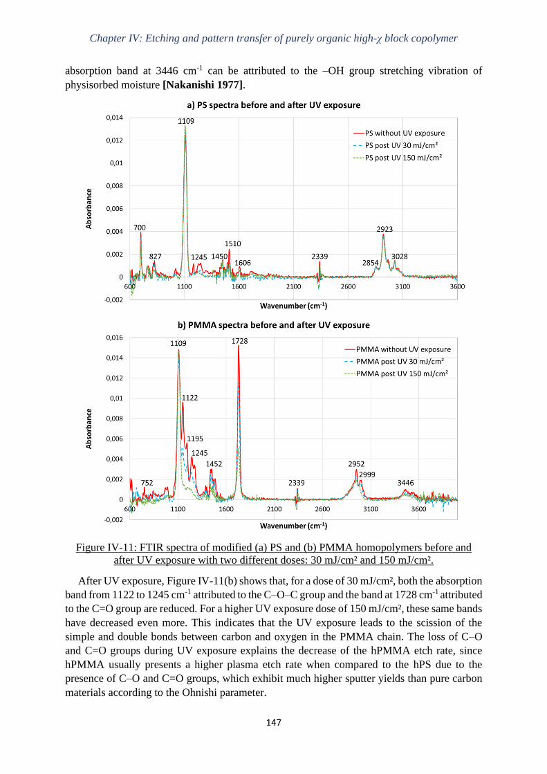
Chapter IV: Etching and pattern transfer of purely organic high-χ block copolymer
147
absorption band at 3446 cm-1 can be attributed to the –OH group stretching vibration of
physisorbed moisture [Nakanishi 1977].
Figure IV-11: FTIR spectra of modified (a) PS and (b) PMMA homopolymers before and
after UV exposure with two different doses: 30 mJ/cm² and 150 mJ/cm².
After UV exposure, Figure IV-11(b) shows that, for a dose of 30 mJ/cm², both the absorption
band from 1122 to 1245 cm-1 attributed to the C–O–C group and the band at 1728 cm-1 attributed
to the C=O group are reduced. For a higher UV exposure dose of 150 mJ/cm², these same bands
have decreased even more. This indicates that the UV exposure leads to the scission of the
simple and double bonds between carbon and oxygen in the PMMA chain. The loss of C–O
and C=O groups during UV exposure explains the decrease of the hPMMA etch rate, since
hPMMA usually presents a higher plasma etch rate when compared to the hPS due to the
presence of C–O and C=O groups, which exhibit much higher sputter yields than pure carbon
materials according to the Ohnishi parameter.
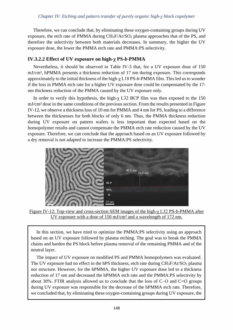
Chapter IV: Etching and pattern transfer of purely organic high-χ block copolymer
148
Therefore, we can conclude that, by eliminating these oxygen-containing groups during UV
exposure, the etch rate of PMMA during CH3F/Ar/SO2 plasma approaches that of the PS, and
therefore the selectivity between both materials decreases. In summary, the higher the UV
exposure dose, the lower the PMMA etch rate and PMMA:PS selectivity.
IV.3.2.2 Effect of UV exposure on high-χ PS-b-PMMA
Nevertheless, it should be observed in Table IV-3 that, for a UV exposure dose of 150
mJ/cm², hPMMA presents a thickness reduction of 17 nm during exposure. This corresponds
approximately to the initial thickness of the high-χ L18 PS-b-PMMA film. This led us to wonder
if the loss in PMMA etch rate for a higher UV exposure dose could be compensated by the 17-
nm thickness reduction of the PMMA caused by the UV exposure only.
In order to verify this hypothesis, the high-χ L32 BCP film was then exposed to the 150
mJ/cm² dose in the same conditions of the previous section. From the results presented in Figure
IV-12, we observe a thickness loss of 10 nm for PMMA and 4 nm for PS, leading to a difference
between the thicknesses for both blocks of only 6 nm. Thus, the PMMA thickness reduction
during UV exposure on pattern wafers is less important than expected based on the
homopolymer results and cannot compensate the PMMA etch rate reduction caused by the UV
exposure. Therefore, we can conclude that the approach based on an UV exposure followed by
a dry removal is not adapted to increase the PMMA:PS selectivity.
Figure IV-12: Top-view and cross-section SEM images of the high-χ L32 PS-b-PMMA after
UV exposure with a dose of 150 mJ/cm² and a wavelength of 172 nm.
In this section, we have tried to optimize the PMMA:PS selectivity using an approach
based on an UV exposure followed by plasma etching. The goal was to break the PMMA
chains and harden the PS block before plasma removal of the remaining PMMA and of the
neutral layer.
The impact of UV exposure on modified PS and PMMA homopolymers was evaluated.
The UV exposure had no effect in the hPS thickness, etch rate during CH3F/Ar/SO2 plasma
nor structure. However, for the hPMMA, the higher UV exposure dose led to a thickness
reduction of 17 nm and decreased the hPMMA etch rate and the PMMA:PS selectivity by
about 30%. FTIR analysis allowed us to conclude that the loss of C–O and C=O groups
during UV exposure was responsible for the decrease of the hPMMA etch rate. Therefore,
we concluded that, by eliminating these oxygen-containing groups during UV exposure, the

Chapter IV: Etching and pattern transfer of purely organic high-χ block copolymer
149
IV.3.3 Third approach: oxygen-free PMMA removal
In section IV.2.2 we have seen that the oxygen-free PMMA removal based on CH4/N2
presents the best PMMA:PS selectivity for the high-χ PS-b-PMMA among the evaluated
plasma processes. In this section, we propose to explore this CH4/N2 PMMA removal as the
third approach for optimizing the PMMA:PS selectivity while also avoiding bridge formation.
We shall begin by varying the CH4/N2 ratio applied to modified PS and PMMA
homopolymers in order to evaluate the process window of this dry etch chemistry. The etch
mechanisms shall also be determined thanks to X-ray photoelectron spectroscopy (XPS). Then,
the results obtained for the 18-nm pitch high-χ PS-b-PMMA will be presented, highlighting the
challenges encountered due to its smaller dimensions.
IV.3.3.1 Application to modified PS and PMMA homopolymers
Figure IV-13 summarizes the high-χ modified PS and PMMA homopolymer consumption
as a function of plasma process time for different CH4/N2 ratios. All of the experiments were
performed in the 300 mm Kiyo FX® ICP reactor from LamResearch®. The pressure, RF bias
and RF power are the ones presented in Table IV-1. Ratio 1:1 corresponds to the recipe
presented in said table, with the CH4/N2 flow corresponding to 50/50 sccm. Ratio 1:2
corresponds to CH4/N2 25/50 sccm, while ratio 2:1 corresponds to CH4/N2 50/25 sccm.
The graph in Figure IV-13 shows that, for the ratio 1:2, both materials consumptions are
linear. After 60 seconds of etching, around 42 nm of PMMA and 9 nm of PS are etched,
corresponding to a selectivity of 4.7, approximately. As for the ratio 1:1, after 60 seconds, 16
nm of PMMA are etched while a deposition of around 5 nm is observed on top of PS, which
means the ratio 1:1 presents infinite selectivity on blanket wafers. Finally, ratio 2:1 presents the
same tendencies as ratio 1:1. However, for the PMMA consumption, it seems to reach a plateau
after 25 seconds of etching.
These results indicate that CH4 is the major passivating component of this etching chemistry,
since the ratio 1:2, which presents less CH4 (25 sccm) when compared to the other two ratios
etch rate of hPMMA during CH3F/Ar/SO2 plasma approaches that of the hPS, and therefore
the selectivity between both materials decreases. In summary, the higher the UV exposure
dose, the lower the PMMA etch rate and PMMA:PS selectivity.
Nevertheless, the 17-nm thickness loss of hPMMA during UV exposure corresponds
approximately to the initial thickness of the high-χ L18 PS-b-PMMA film. Thus, the high-
χ L32 BCP was used to verify if the loss in PMMA etch rate for a higher UV exposure dose
could be compensated by the 17-nm thickness reduction of the PMMA caused by the UV
exposure only. However, after an UV exposure with a dose of 150 mJ/cm², the difference
between the thicknesses of both blocks with the lamellar BCP was only 6 nm, which does
not compensate the PMMA etch rate reduction. Therefore, we concluded that the approach
based on an UV exposure followed by a dry removal was not adapted to increase the
PMMA:PS selectivity.

Chapter IV: Etching and pattern transfer of purely organic high-χ block copolymer
150
(50 sccm), is also the one that presents higher etch rate for both PS and PMMA. Thus, nitrogen
(N2) seems to be the main etching component.
Figure IV-13: Modified PS and PMMA homopolymer consumption for different CH4/N2
ratios. The yellow zone corresponds to the etching zone while the blue zone corresponds to
the deposition zone.
In order to understand the etching mechanisms and plasma/surface interactions involved,
quasi in-situ XPS analysis were carried out on these blanket high-χ homopolymers for ratios
1:1 and 1:2 with different etching times. The results for the surface composition of hPS and
hPMMA after etching are shown in Figure IV-14. The as deposited composition is also
presented for comparison purposes.
First, it should be reminded that the composition of the as deposited high-χ PS and PMMA
homopolymers has already been detailed in section IV.1.1 (Figure IV-2) and that they present
a composition very similar to that of the standard PS and PMMA. After etching, Figures IV-
14(a) and (c) represent the ratio 1:1, while Figures IV-14(b) and (d) represent the ratio 1:2.
These results correspond to an angle of 76.25° from the normal incidence, meaning it represents
mostly the first 2 nm of the surface. It is important to notice the presence of two new peaks on
both materials after etching. A C-N peak appears at 286 eV which, due to spectral resolution,
cannot be differentiated from C-O (286.5 eV) bonds and is thus represented together as C-O/C-
N. The presence of this bond is confirmed by the apparition of an N-C peak on the N1s spectra
at 399.4 eV [Beamson 1992]. We should also notice that, for the two different CH4/N2 ratios,
the surface composition of both polymers is already modified from the first seconds of etching.
When we observe the results after CH4/N2 plasma with ratio 1:1 for the PS surface presented
in Figure IV-14(a), the pi→pi* shake-up peak is no longer present for all the etching durations.
Moreover, as we increase the etching duration, there is an increase in the percentage of C-N
and N-C bonds and decrease of C-C/C=C bonds. This indicates that a CN-type deposit forms
on the PS surface and increases in thickness over time, preventing the etching of the PS layer.
Therefore, N2 also participates on the passivation of PS. Moreover, thanks to the quasi in-situ

Chapter IV: Etching and pattern transfer of purely organic high-χ block copolymer
151
XPS technique, almost no oxygen is detected after etching and its atomic percentage is
represented together for both O-C and O=C.
Figure IV-14: Surface composition of modified (a, b) PS and (c, d) PMMA homopolymers
obtained by quasi in-situ XPS for two different ratios: (a, c) ratio 1:1, and (b, d) ratio 1:2. The
results correspond to an incident angle of 76.25°.
As for the PMMA after CH4/N2 plasma with ratio 1:1, Figure IV-14(c) shows a loss of O-C
and O=C bonds, which goes from a total atomic percentage of oxygen of 27.3% to 2.4% after
60 seconds of etching. The C=O C1s peak is also reduced from 9.5% to 1.8% after the same
etching duration. This loss of carbon-oxygen simple and double bonds is characteristic of
PMMA consumption. We also observed the presence of the C-N bonds after etching, which
could explain the decrease of the PMMA etch rate with time. Indeed, from the graph in Figure
IV-13, we see that, after 5 seconds of PMMA etching with ratio 1:1, around 10 nm of PMMA
were consumed, while for 60 seconds only 16 nm were etched. This confirms our observation
that, depending on the CH4/N2 ratio and etching duration, N2 participates in both the etching
and passivation of PMMA and PS.
For the CH4/N2 plasma with ratio 1:2, we can observe on Figures IV-14(b) and (d) that the
etching presents the same tendencies as the ratio 1:1 with a higher C-N content, which is to be
expected from the increase of the N2 flow. These same etching mechanisms were observed for
standard PS-b-PMMA in previous works [Sarrazin 2019].

Chapter IV: Etching and pattern transfer of purely organic high-χ block copolymer
152
IV.3.3.2 Application to PS-b-PMMA films with lamellar morphology
The oxygen-free PMMA removal based on a CH4/N2 plasma was first validated using a
standard PS-b-PMMA with intrinsic period L0 = 38 nm supplied by Arkema. The BCP solution
is spin-coated and annealed on 300 mm wafers using the Sokudo DUO™ DSA-dedicated track.
As we have seen for the other block copolymers, a thin neutral layer composed of PS-r-PMMA
random copolymer is spin-coated on the substrate before the BCP deposition in order to
neutralize the surface and obtain the vertical lamellae morphology. The neutral and BCP layer
thicknesses are around 8 and 52 nm, respectively. Figure IV-15 presents the cross-section and
top-view SEM images post PMMA removal, as well as the calculated selectivity for the
different CH4/N2 ratios applied to this block copolymer in order to compare the PMMA:PS
selectivity of free surface and blanket wafers.
Figure IV-15: Cross-section and top-view SEM images of standard PS-b-PMMA with 38-nm
pitch after etching with different CH4/N2 ratios: (a) ratio 1:2; (b) ratio 1:1; and (c) ratio 2:1.
The calculated PMMA:PS selectivity is also indicated for each ratio.
As expected, the greater the CH4 content, the better the selectivity since CH4 is the major
passivating component of this etching chemistry. However, Figure IV-15(c) shows that when
the CH4/N2 ratio is too important, the PS lines thickness is increased due to too much carbon
passivation on the PS flanks. The highlighted section on the top-view image in Figure IV-15(c)
presents the consequent pattern collapse caused by the lines thickening, which will prevent the

Chapter IV: Etching and pattern transfer of purely organic high-χ block copolymer
153
correct pattern transfer into the hard mask. Therefore, we selected the ratios 1:2 and 1:1, which
present a PMMA:PS selectivity of 2.7 and 7.0, respectively, to continue our studies for the high-
χ PS-b-PMMA.
It is also important to notice that, for all CH4/N2 ratios studied, the selectivity on free surface
is lower compared to that of blanket wafers. For example, the ratio 1:1 PMMA:PS selectivity
decreases from infinite on homopolymers to around 7.0 for the standard PS-b-PMMA with 38-
nm pitch. This difference between block copolymer and homopolymer etching regarding the
PS consumption has already been observed in section IV.2.2 and indicates that the oxygen-
containing by-products of the PMMA etching probably interact with the PS phase, inducing its
consumption.
For the etching of the 18-nm pitch high-χ PS-b-PMMA, we have estimated at the beginning
of this chapter that there should be at least 15 nm of PS plus neutral layer left after PMMA
removal to ensure the correct pattern transfer into the silicon oxide hard mask. This means that
the high-χ L18 BCP requires a higher selectivity than the standard PS-b-PMMA that we have
just evaluated due to the L18’s reduced initial thickness (16 nm). Since the initial thickness of
the PS-b-PMMA and neutral layer stack is approximately 21 nm, this translates to a desired
selectivity of around 3.5.
Figure IV-16 presents the cross-section and top-view SEM images after PMMA removal
using CH4/N2 with ratio 1:2 and 1:1 for the high-χ L18 BCP, as well as the calculated selectivity
for each ratio. First, it is important to notice that, for the same dry process, the 18-nm pitch
high-χ BCP presents lower selectivity compared to the 38-nm pitch standard PS-b-PMMA,
which we had already observed in Figure IV-4 for the 32-nm pitch high-χ BCP. We have seen
in Figure IV-3 that, for two PS-b-PMMA with the same intrinsic period but different chemistry,
there is no difference in selectivity for the same plasma etching chemistry between both BCPs.
Thus, this difference observed in selectivity between the high-χ L18 and the standard L38 is
probably not caused by the modified chemistry of the high-χ BCP. However, it might be due to
to the fact that the etching time is shorter for smaller thickness. It should also be noticed that
the cross-section SEM measurements are approximations, due to the tool’s low precision when
using higher magnification.
Figure IV-16(a) shows the results for the CH4/N2 plasma with ratio 1:2, which presents a
selectivity of around 1.4. As we have established before, with the block copolymer’s reduced
21-nm initial thickness, such low selectivity means there is not enough PS budget for pattern
transfer. However, the results in Figure IV-7 have shown us that, when the PS-b-PMMA initial
thickness is increased to 35 nm, pattern wiggling is observed after PMMA removal due to the
high aspect ratio of the lines.
As for the CH4/N2 plasma with ratio 1:1, the results have already been presented in Figure
IV-4 and detailed in section IV.2.2. They have been reproduced again in Figure IV-16(b) to
highlight the formation of bridges on top of the lines pattern, which prevents correct pattern
transfer into the SiO2 hard mask, as we have seen in Figure IV-5. These bridges were not present
on the 38-nm pitch standard PS-b-PMMA shown in Figure IV-15(b). They might have come
from the modified PS-b-PMMA chemistry of the high-χ BCP, except they were not observed
after CH3F/Ar/SO2 plasma in Figures IV-4 nor IV-6. Therefore, they are probably formed due
to intensive sidewalls passivation during the CH4/N2 plasma and to a species confinement
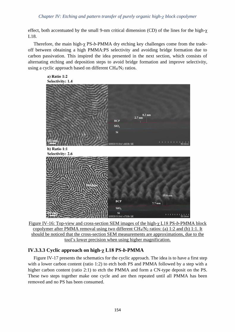
Chapter IV: Etching and pattern transfer of purely organic high-χ block copolymer
154
effect, both accentuated by the small 9-nm critical dimension (CD) of the lines for the high-χ
L18.
Therefore, the main high-χ PS-b-PMMA dry etching key challenges come from the trade-
off between obtaining a high PMMA:PS selectivity and avoiding bridge formation due to
carbon passivation. This inspired the idea presented in the next section, which consists of
alternating etching and deposition steps to avoid bridge formation and improve selectivity,
using a cyclic approach based on different CH4/N2 ratios.
Figure IV-16: Top-view and cross-section SEM images of the high-χ L18 PS-b-PMMA block
copolymer after PMMA removal using two different CH4/N2 ratios: (a) 1:2 and (b) 1:1. It
should be noticed that the cross-section SEM measurements are approximations, due to the
tool’s lower precision when using higher magnification.
IV.3.3.3 Cyclic approach on high-χ L18 PS-b-PMMA
Figure IV-17 presents the schematics for the cyclic approach. The idea is to have a first step
with a lower carbon content (ratio 1:2) to etch both PS and PMMA followed by a step with a
higher carbon content (ratio 2:1) to etch the PMMA and form a CN-type deposit on the PS.
These two steps together make one cycle and are then repeated until all PMMA has been
removed and no PS has been consumed.

Chapter IV: Etching and pattern transfer of purely organic high-χ block copolymer
155
Figure IV-17: Schematics for the cyclic approach with different CH4/N2 ratios in order to
completely remove the PMMA selectively to PS.
First, this cyclic approach was tested on modified PS and PMMA homopolymers. Figure IV-
18 presents the homopolymer consumption for the cyclic approach with a first 5-seconds
CH4/N2 step with ratio 1:2 followed by a second 5-seconds CH4/N2 step with ratio 2:1. The
yellow zone corresponds to the etching zone while the blue zone corresponds to the deposition
zone. The graph shows that the PMMA is continuously etched with the increasing number of
cycles. After 4 cycles, around 23 nm of PMMA have been etched, which is greater than the
initial thickness of the PMMA + neutral layer stack for the high-χ L18 BCP. Figure IV-18 also
shows that the PS is not consumed after 4 cycles, thus validating the schematics presented in
Figure IV-17 for PS and PMMA homopolymers.
Figure IV-18: Modified PS and PMMA homopolymer consumption for the cyclic approach
with a first 5-seconds CH4/N2 step with ratio 1:2 followed by a second 5-seconds CH4/N2 step
with ratio 2:1. The yellow zone corresponds to the etching zone while the blue zone
corresponds to the deposition zone.
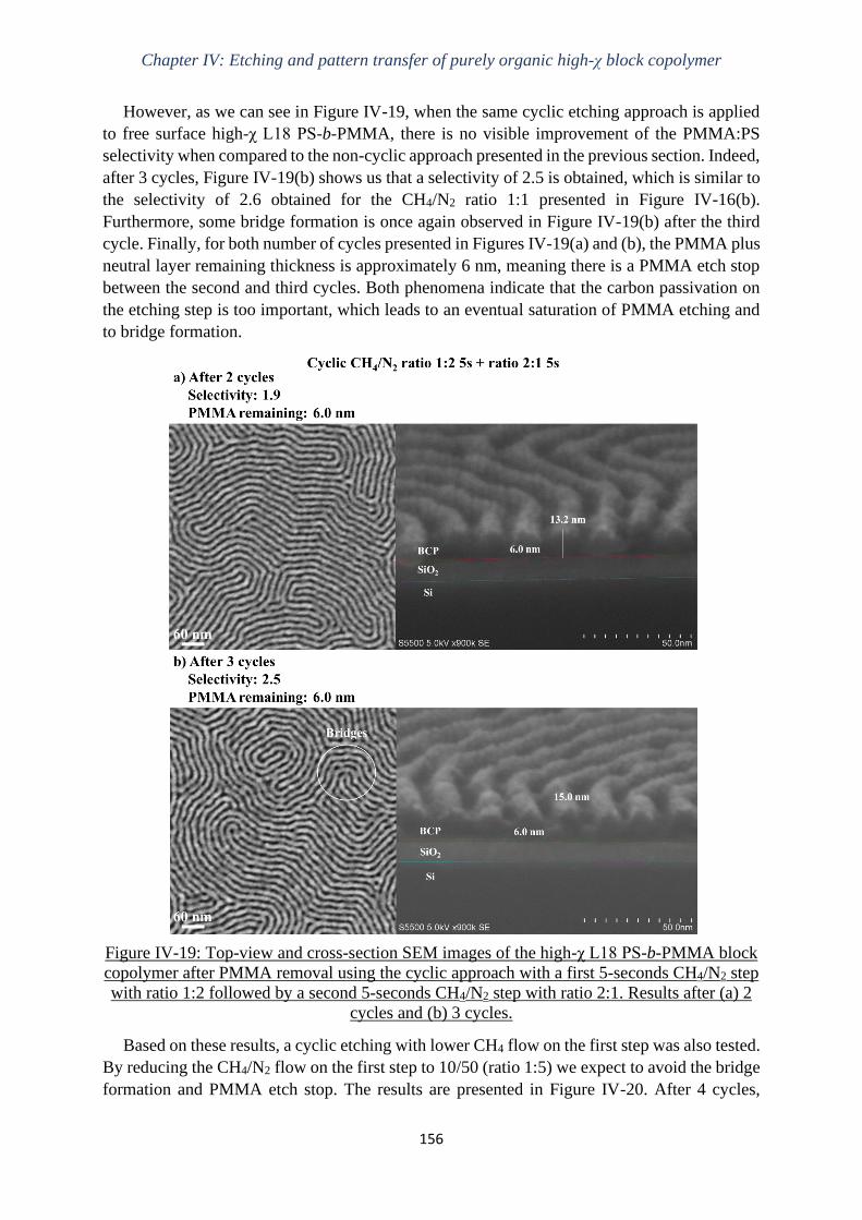
Chapter IV: Etching and pattern transfer of purely organic high-χ block copolymer
156
However, as we can see in Figure IV-19, when the same cyclic etching approach is applied
to free surface high-χ L18 PS-b-PMMA, there is no visible improvement of the PMMA:PS
selectivity when compared to the non-cyclic approach presented in the previous section. Indeed,
after 3 cycles, Figure IV-19(b) shows us that a selectivity of 2.5 is obtained, which is similar to
the selectivity of 2.6 obtained for the CH4/N2 ratio 1:1 presented in Figure IV-16(b).
Furthermore, some bridge formation is once again observed in Figure IV-19(b) after the third
cycle. Finally, for both number of cycles presented in Figures IV-19(a) and (b), the PMMA plus
neutral layer remaining thickness is approximately 6 nm, meaning there is a PMMA etch stop
between the second and third cycles. Both phenomena indicate that the carbon passivation on
the etching step is too important, which leads to an eventual saturation of PMMA etching and
to bridge formation.
Figure IV-19: Top-view and cross-section SEM images of the high-χ L18 PS-b-PMMA block
copolymer after PMMA removal using the cyclic approach with a first 5-seconds CH4/N2 step
with ratio 1:2 followed by a second 5-seconds CH4/N2 step with ratio 2:1. Results after (a) 2
cycles and (b) 3 cycles.
Based on these results, a cyclic etching with lower CH4 flow on the first step was also tested.
By reducing the CH4/N2 flow on the first step to 10/50 (ratio 1:5) we expect to avoid the bridge
formation and PMMA etch stop. The results are presented in Figure IV-20. After 4 cycles,
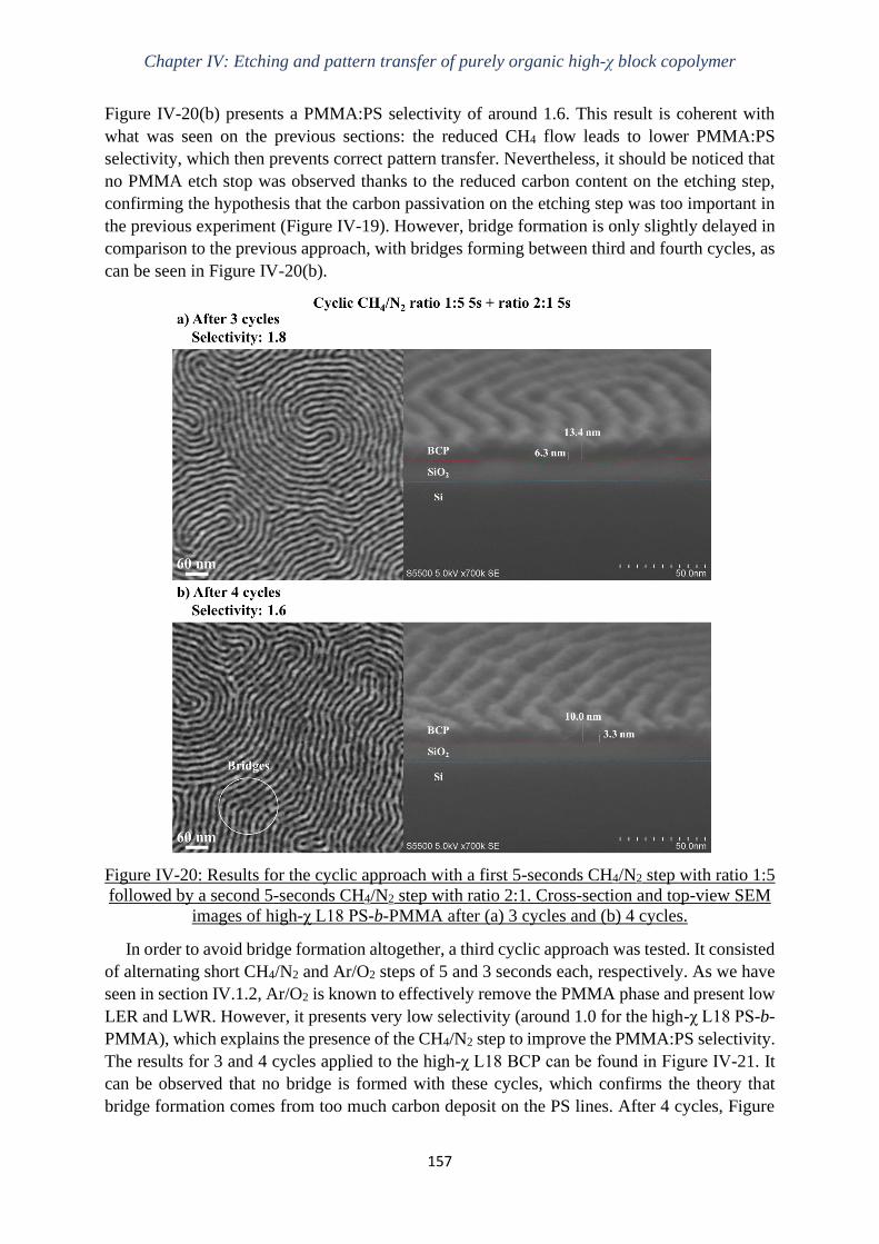
Chapter IV: Etching and pattern transfer of purely organic high-χ block copolymer
157
Figure IV-20(b) presents a PMMA:PS selectivity of around 1.6. This result is coherent with
what was seen on the previous sections: the reduced CH4 flow leads to lower PMMA:PS
selectivity, which then prevents correct pattern transfer. Nevertheless, it should be noticed that
no PMMA etch stop was observed thanks to the reduced carbon content on the etching step,
confirming the hypothesis that the carbon passivation on the etching step was too important in
the previous experiment (Figure IV-19). However, bridge formation is only slightly delayed in
comparison to the previous approach, with bridges forming between third and fourth cycles, as
can be seen in Figure IV-20(b).
Figure IV-20: Results for the cyclic approach with a first 5-seconds CH4/N2 step with ratio 1:5
followed by a second 5-seconds CH4/N2 step with ratio 2:1. Cross-section and top-view SEM
images of high-χ L18 PS-b-PMMA after (a) 3 cycles and (b) 4 cycles.
In order to avoid bridge formation altogether, a third cyclic approach was tested. It consisted
of alternating short CH4/N2 and Ar/O2 steps of 5 and 3 seconds each, respectively. As we have
seen in section IV.1.2, Ar/O2 is known to effectively remove the PMMA phase and present low
LER and LWR. However, it presents very low selectivity (around 1.0 for the high-χ L18 PS-b-
PMMA), which explains the presence of the CH4/N2 step to improve the PMMA:PS selectivity.
The results for 3 and 4 cycles applied to the high-χ L18 BCP can be found in Figure IV-21. It
can be observed that no bridge is formed with these cycles, which confirms the theory that
bridge formation comes from too much carbon deposit on the PS lines. After 4 cycles, Figure

Chapter IV: Etching and pattern transfer of purely organic high-χ block copolymer
158
IV-21(b) shows that the PMMA is completely removed, however there is not enough PS
remaining (around 7 nm) for pattern transfer into the SiO2 hard mask.
Therefore, we conclude that the cyclic approach still presents the same etching difficulties
that we observed for the non-cyclic process. This means the full dry etching approach cannot
find the right balance between high selectivity and bridge formation for the high-χ L18 PS-b-
PMMA, mostly due to its small dimensions, namely its initial thickness and pitch.
Figure IV-21: Results for the cyclic approach with a first 5-seconds CH4/N2 step with ratio 1:1
followed by a second 3-seconds Ar/O2 step with ratio 24:1. Cross-section and top-view SEM
images of high-χ L18 PS-b-PMMA after (a) 3 cycles and (b) 4 cycles.
In this section, we have tried to optimize the oxygen-free PMMA removal based on
CH4/N2, which presented the best selectivity for the high-χ L18, but also some bridge
formation on top of the lines.
The impact of the CH4/N2 ratio variation was evaluated on PS and PMMA
homopolymers. For ratios 1:1 and 2:1, the PMMA was etched and a deposited layer was
formed over the PS, leading to an infinite PMMA:PS selectivity. The etching and deposition
mechanisms were determined by XPS. For the PS, a CN-type deposit forms on the PS
surface and increases in thickness over time, preventing the etching of the PS layer. For the
PMMA, a loss of C-O and C=O bonds was observed, which is characteristic of PMMA etch.

Chapter IV: Etching and pattern transfer of purely organic high-χ block copolymer
159
IV.3.4 Fourth approach: mixed wet and dry etching
The PMMA removal by aqueous solution has been considered an interesting approach in
order not to damage the PS. The principle is to use a solvent for which one of the blocks of the
BCP is soluble while the other is insoluble. Thus, the soluble polymer dissolves in the presence
of the solvent while the other phase is not altered by it.
Gharbi et al. have evaluated the interest of UV exposure as well as the impact of the dose
used on cylindrical PS-b-PMMA. In their study, they have shown that, when acetic acid is used
without UV exposure, a surface reconstruction of the block copolymer occurs: PMMA chains
migrate from the cylindrical domains to the top surface and remain tethered to the PS chains.
This leads to an increase of the BCP thickness and surface roughness. They conclude that
certain covalent bonds between the two blocks of the copolymer were not broken during acetic
acid rinsing, and therefore the use of the solvent alone does not allow the scission of the chains,
leading to the addition of an UV exposure step. They then show that, depending on the UV
exposure dose used, the thickness of the polymer after acetic acid rinsing may be greater than
the initial thickness (low doses) or lower (high doses). Therefore, when an UV exposure is
conducted with a sufficient dose before acetic acid rinsing, a flat surface is obtained and the
BCP thickness decreases. This shows that UV exposure leads to the degradation of the PMMA
block via chains scission and the cleavage of the PS/PMMA covalent bonds, so that PMMA
We also observed the presence of the C-N bonds after etching, which explains the decrease
of the PMMA etch rate with time.
When applying this chemistry on the lamellar BCP, we observed that, the greater the
CH4 content, the better the PMMA:PS selectivity, indicating that CH4 is the major
passivating component of this etching chemistry. However, for the ratio 2:1, the PS lines
thickness was increased due to too much carbon passivation on the PS flanks, which led to
pattern collapse. Ratio 1:2 presented a selectivity of around 1.4 for the high-χ L18. Such
low selectivity means there is not enough PS budget for pattern transfer. Finally, ratio 1:1
presented a selectivity of 2.6, but bridges were formed on top of the lines pattern, which
prevented correct pattern transfer into the SiO2 hard mask. These bridges were probably
formed due to intensive sidewalls passivation during the CH4/N2 plasma and to a species
confinement effect, both accentuated by the small 9-nm critical dimension (CD) of the lines
for the high-χ L18.
Therefore, we concluded that the main high-χ PS-b-PMMA dry etching key challenges
come from the trade-off between obtaining a high PMMA:PS selectivity and avoiding
bridge formation due to carbon passivation.
We then tried using a cyclic approach based on different CH4/N2 ratios, which consisted
of alternating etching and deposition steps to avoid bridge formation and improve
selectivity. However, the results showed that the cyclic approach still presents the same
etching difficulties observed for the non-cyclic process. Therefore, the full dry etching
approach cannot find the right balance between high selectivity and bridge formation for
the high-χ L18 PS-b-PMMA, mostly due to its small dimensions, namely its initial thickness
and pitch.

Chapter IV: Etching and pattern transfer of purely organic high-χ block copolymer
160
can be completely removed after the wet development. It also reportedly permits the cross-
linking of PS and the reduction of its solubility [Gharbi 2015].
Based on the results obtained in the previous sections with the full dry approach, in this
section we have proposed a mixed wet and dry etching approach in order to successfully remove
the PMMA and open the neutral layer, conserving enough PS budget for pattern transfer. This
approach consists of a wet PMMA removal in order to obtain an infinite PMMA:PS selectivity,
followed by a dry neutral layer opening step to allow for pattern transfer into the SiO2 layer.
The schematics for this approach is presented in Figure IV-22. The main difference between
this approach and the full dry approach is that the UV exposure + wet removal does not remove
the neutral layer, which has to be removed through dry etching.
Figure IV-22: Schematics for the flow used in the mixed wet and dry etching approach for the
18-nm pitch high-χ PS-b-PMMA block copolymer.
IV.3.4.1 PMMA removal through UV exposure followed by wet rinsing
The wet PMMA removal for the high-χ L18 PS-b-PMMA consists of two steps: an UV
exposure followed by a solvent rinse. With the appropriate dose, the UV exposure is responsible
for both breaking the PMMA chains and the PS/PMMA covalent bond, which allows these
broken chains to be later removed by the solvent rinse, and hardening the PS lines, which helps
avoid possible pattern collapse due to capillary forces. The optimal dose was found by the
lithography team to be 30 mJ/cm² with a 172 nm wavelength. Similarly to section IV.3.2, the
UV exposure was conducted in the Sokudo DUO tool. As for the second step, the solvent chosen
was isopropyl alcohol (IPA), which dissolves the PMMA without modifying the PS. The rinse
time is set at 30 seconds.
Figure IV-23: Top-view and cross-section SEM images of high-χ L18 PS-b-PMMA after
PMMA removal through UV exposure followed by IPA rinsing.
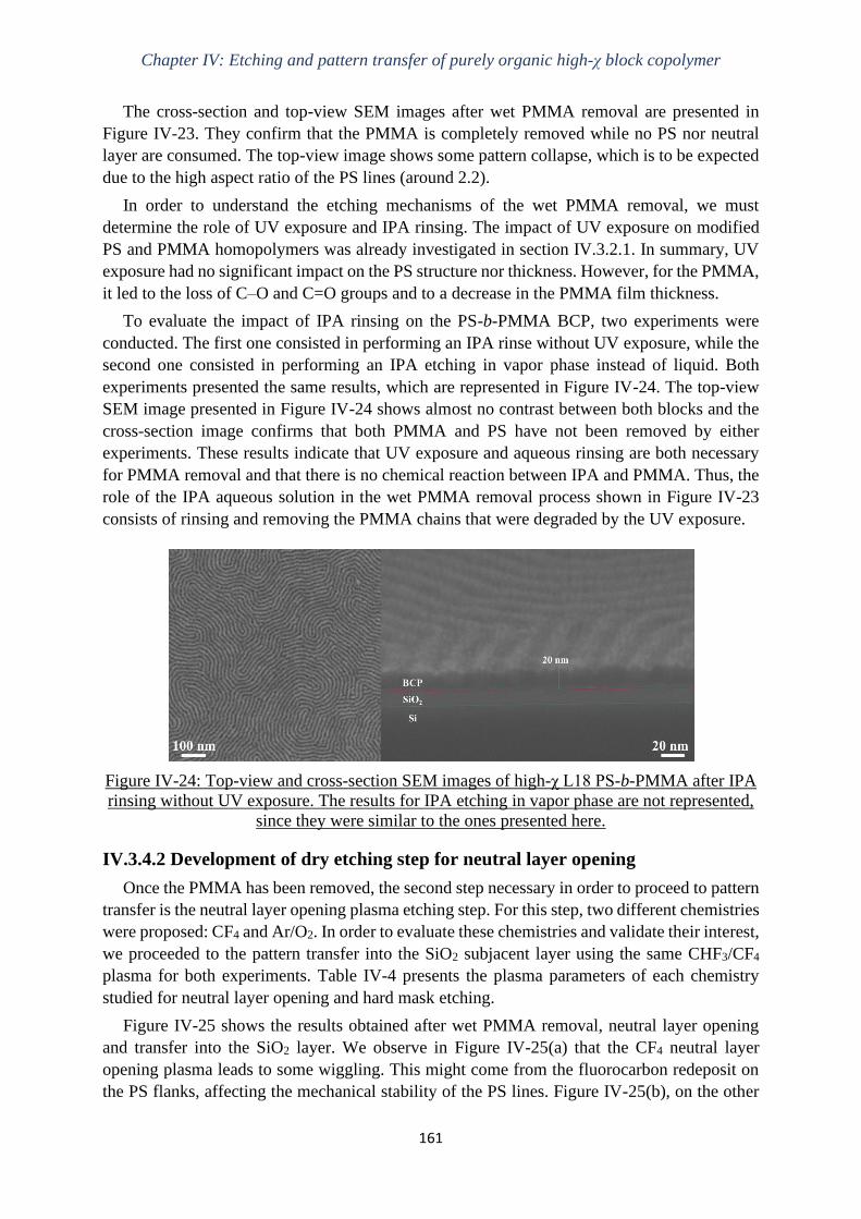
Chapter IV: Etching and pattern transfer of purely organic high-χ block copolymer
161
The cross-section and top-view SEM images after wet PMMA removal are presented in
Figure IV-23. They confirm that the PMMA is completely removed while no PS nor neutral
layer are consumed. The top-view image shows some pattern collapse, which is to be expected
due to the high aspect ratio of the PS lines (around 2.2).
In order to understand the etching mechanisms of the wet PMMA removal, we must
determine the role of UV exposure and IPA rinsing. The impact of UV exposure on modified
PS and PMMA homopolymers was already investigated in section IV.3.2.1. In summary, UV
exposure had no significant impact on the PS structure nor thickness. However, for the PMMA,
it led to the loss of C–O and C=O groups and to a decrease in the PMMA film thickness.
To evaluate the impact of IPA rinsing on the PS-b-PMMA BCP, two experiments were
conducted. The first one consisted in performing an IPA rinse without UV exposure, while the
second one consisted in performing an IPA etching in vapor phase instead of liquid. Both
experiments presented the same results, which are represented in Figure IV-24. The top-view
SEM image presented in Figure IV-24 shows almost no contrast between both blocks and the
cross-section image confirms that both PMMA and PS have not been removed by either
experiments. These results indicate that UV exposure and aqueous rinsing are both necessary
for PMMA removal and that there is no chemical reaction between IPA and PMMA. Thus, the
role of the IPA aqueous solution in the wet PMMA removal process shown in Figure IV-23
consists of rinsing and removing the PMMA chains that were degraded by the UV exposure.
Figure IV-24: Top-view and cross-section SEM images of high-χ L18 PS-b-PMMA after IPA
rinsing without UV exposure. The results for IPA etching in vapor phase are not represented,
since they were similar to the ones presented here.
IV.3.4.2 Development of dry etching step for neutral layer opening
Once the PMMA has been removed, the second step necessary in order to proceed to pattern
transfer is the neutral layer opening plasma etching step. For this step, two different chemistries
were proposed: CF4 and Ar/O2. In order to evaluate these chemistries and validate their interest,
we proceeded to the pattern transfer into the SiO2 subjacent layer using the same CHF3/CF4
plasma for both experiments. Table IV-4 presents the plasma parameters of each chemistry
studied for neutral layer opening and hard mask etching.
Figure IV-25 shows the results obtained after wet PMMA removal, neutral layer opening
and transfer into the SiO2 layer. We observe in Figure IV-25(a) that the CF4 neutral layer
opening plasma leads to some wiggling. This might come from the fluorocarbon redeposit on
the PS flanks, affecting the mechanical stability of the PS lines. Figure IV-25(b), on the other

Chapter IV: Etching and pattern transfer of purely organic high-χ block copolymer
162
hand, shows that the Ar/O2 plasma was too aggressive and, while completely removing the
neutral layer, it also consumed too much PS. Therefore, it did not conserve enough PS + neutral
layer budget for complete pattern transfer into the silicon oxide hard mask.
Table IV-4. Plasma parameters of the chemistries tested for the dry etching of the neutral and
SiO2 layers.
Etching Pressure (mTorr) Power (W) Bias (V) Flow (sccm) Time (s)
CF4 10 625 -70 150 5
Ar/O2 10 220 -200 50/5 5
CHF3/CF4 4 625 -110 50/50 8
Figure IV-25: Top-view and cross-section SEM images of high-χ L18 PS-b-PMMA after the
wet PMMA removal, the neutral layer dry opening (represented as “BT” for breakthrough
step) and the SiO2 etching. Two different neutral layer opening plasmas are presented: (a) CF4
and (b) Ar/O2 with ratio 10:1.
The Ar/O2 ratio was then improved to 24:1 (120/5 sccm) instead of 10:1 (50/5 sccm) while
conserving the other parameters presented in Table IV-4. This ratio improvement is expected
to provide a less isotropic etching and to conserve more PS budget. Figure IV-26(a) presents
the top-view and cross-section SEM images after wet PMMA removal, neutral layer opening
with Ar/O2 ratio 24:1, SiO2 etching with CHF3/CF4 and PS stripping with an oxygen plasma. It

Chapter IV: Etching and pattern transfer of purely organic high-χ block copolymer
163
confirms what was expected: increasing the argon content improved the neutral layer:PS
selectivity and allowed for complete pattern transfer into the SiO2.
Finally, Figure IV-26(b) presents the results after the complete stack etching: wet PMMA
removal with UV exposure followed by IPA rinsing, dry neutral layer opening using the
optimized Ar/O2 plasma, SiO2 etching using the CHF3/CF4 plasma, Si bulk layer etching with
an HBr/O2 plasma, and remaining PS stripping with an O2 plasma. The lines pattern has been
transferred into 13.8 nm of silicon bulk with a CD of 11 nm (CD bias ~ 2 nm). Therefore, we
demonstrate the pattern transfer of an 18-nm pitch high-χ organic block copolymer into SiO2
and silicon bulk layers using a mixed wet and dry etching removal process.
Figure IV-26: Top-view and cross-section SEM images of high-χ L18 PS-b-PMMA (a) after
the wet PMMA removal, the neutral layer dry opening with Ar/O2 ratio 24:1 and the SiO2
etching; and (b) the partial transfer into the silicon bulk. For both cross-section images, the PS
has been stripped with an oxygen plasma before imaging.
In this section, we have explored a mixed wet and dry etching approach for the PMMA
removal and transfer into the hard mask. This approach consisted of a wet PMMA removal
in order to obtain an infinite PMMA:PS selectivity, followed by a dry neutral layer opening
step to allow for pattern transfer into the SiO2 layer.
The wet PMMA removal was validated using an UV exposure with wavelength 172 nm
and dose 30 mJ/cm². The UV exposure is responsible for the degradation of the PMMA
block via chains scission and the cleavage of the PS/PMMA covalent bonds. After UV, an

Chapter IV: Etching and pattern transfer of purely organic high-χ block copolymer
164
IV.4 Conclusions
In this chapter, we have studied the PMMA removal selectively to PS on high-χ PS-b-
PMMA films with an 18-nm pitch. We started by characterizing the composition of the
modified PS and PMMA homopolymers that compose the high-χ modified PS-b-PMMA block
copolymer, which led us to conclude that the modified PS-b-PMMA presents a composition
similar to that of standard PS-b-PMMA. Then, we selected different plasma chemistries and we
evaluated their etch rate, and consequent selectivity, on modified PS and PMMA
homopolymers, therefore selecting two different chemistries that fulfill our selectivity
requirement: CH3F/Ar/SO2 and CH4/N2.
We then characterized the impact of the modified chemistry, pitch and initial thickness on
the etching of the high-χ modified PS-b-PMMA. When comparing a modified and a standard
PS-b-PMMA BCP with the same pitch and initial thickness, we concluded that, for the same
plasma etching chemistry, the high-χ modified PS-b-PMMA chemistry does not present a
significant impact on the PMMA plasma etching when compared to the standard PS-b-PMMA
block copolymer. However, when comparing the high-χ modified PS-b-PMMA with two
different pitch (18 and 32 nm) and two different initial thicknesses (16 and 36 nm, respectively),
for the high-χ L18 BCP, the same etching chemistries that were validated for larger pitch (32
nm) present different problems that prevent pattern transfer into the SiO2 hard mask for the
smaller BCP. Therefore, we concluded that the main high-χ L18 PS-b-PMMA plasma etching
challenges come from its small dimensions, namely the pitch and initial thickness.
The next sections focused on developing different approaches in order to improve the
PMMA:PS selectivity. The first approach focused on optimizing the CH3F/Ar/SO2 plasma,
which presented low selectivity (around 1.6) for the high-χ L18, but no bridge formation.
However, we concluded that this plasma presents a very narrow process window regarding the
etch duration due to the small dimensions – pitch and thickness – of the high-χ L18 BCP film.
Varying the etching parameters did not improve the results, nor did the cyclic approach based
on alternating CH3F/Ar/SO2 and Ar steps. Increasing the initial thickness of the high-χ L18 film
led to mechanical stability problems and to pattern wiggling due to the high aspect ratio of the
lines, showing that the smaller CD of the high-χ block copolymer limits the maximum initial
thickness allowed for the BCP film in order to avoid pattern wiggling or collapse. Therefore,
we concluded that the CH3F/Ar/SO2 plasma was not appropriate for the high-χ PS-b-PMMA
etching.
IPA rinsing is conducted to remove the PMMA chains that were degraded by the UV
exposure. This process was shown to completely remove the PMMA while conserving the
PS and the neutral layer.
The next step consisted in the neutral layer dry opening. An Ar/O2 breakthrough step
was developed to open the neutral layer while conserving enough PS budget to validate the
pattern transfer into the silicon oxide hard mask. Finally, the transfer into 13.8 nm of silicon
bulk was also performed, leading to line patterns with a CD of 11 nm (CD bias ~ 2 nm), and
therefore demonstrating the pattern transfer of an 18-nm pitch high-χ organic block
copolymer into SiO2 and silicon bulk layers using a mixed wet and dry etching removal
process.
Chapter IV: Etching and pattern transfer of purely organic high-χ block copolymer
165
The second approach was based on an UV exposure followed by plasma etching. The goal
was to break the PMMA chains and harden the PS block before plasma removal of the
remaining PMMA and of the neutral layer. We showed that the UV exposure had no effect in
the PS. However, for the PMMA, the higher UV exposure dose led to a consumption of 17 nm
and decreased the PMMA etch rate and the PMMA:PS selectivity by about 30%. FTIR analysis
allowed us to conclude that the loss of C–O and C=O groups during UV exposure was
responsible for the decrease of the PMMA etch rate. Therefore, we concluded that, by
eliminating these oxygen-containing groups during UV exposure, the etch rate of PMMA
during CH3F/Ar/SO2 plasma approaches that of the PS, and therefore the selectivity between
both materials decreases. In summary, the higher the UV exposure dose, the lower the PMMA
etch rate and PMMA:PS selectivity. Thus, this approach was not adapted to increase the
PMMA:PS selectivity.
The third approach consisted on optimizing the CH4/N2. While for PS and PMMA
homopolymers we succeeded in etching the PMMA without consuming the PS thanks to a CN-
type deposition layer formed on the PS surface, the same could not be applied to the high-χ PS-
b-PMMA block copolymer assembled on a free surface. The results showed that high-χ BCP
requires higher selectivity than standard PS-b-PMMA due to its smaller thickness. Moreover,
the ratio 1:1, while presenting the best PMMA:PS selectivity without pattern collapse, also
presented some bridge formation on top of the lines, which were formed due to intensive
sidewalls passivation and to a species confinement effect accentuated by the small CD (9 nm).
We then concluded that the main high-χ PS-b-PMMA dry etching difficulties come from the
trade-off between obtaining high selectivity and avoiding bridge formation.
The fourth approach proposed was a mixed wet and dry etching process. The wet PMMA
removal presents infinite selectivity on high-χ modified PS-b-PMMA. The UV exposure causes
the PMMA chains to break and the PS lines to harden, and the IPA rinse removes the broken
PMMA chains without modifying the PS lines. A dry etching process to open the neutral layer
using an Ar/O2 plasma with high argon content was developed in order to obtain a highly
anisotropic etching and to conserve more PS budget. With this mixed wet and dry etching
approach, the complete pattern transfer of an 18-nm pitch high-χ organic block copolymer into
the SiO2 hard mask and silicon bulk layers was validated with CD bias ~ 2 nm.

166

167
CHAPTER V: ETCHING AND PATTERN TRANSFER OF
SILICON-BASED HIGH-χ BLOCK
COPOLYMER
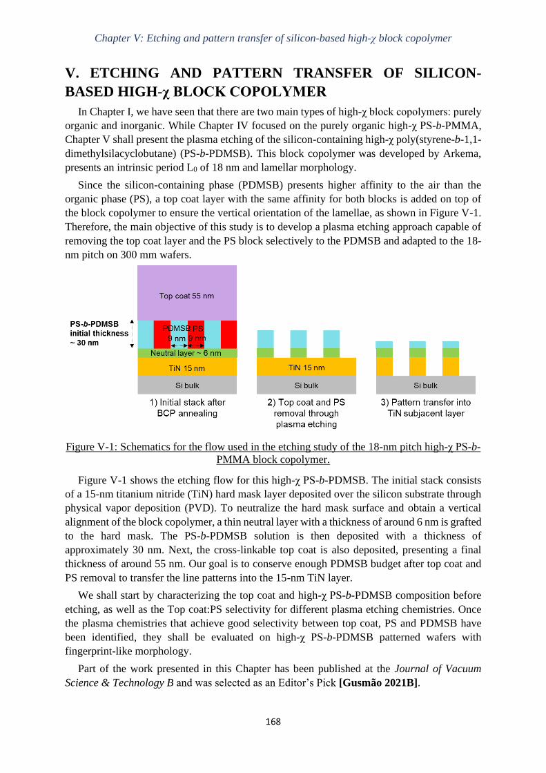
Chapter V: Etching and pattern transfer of silicon-based high-χ block copolymer
168
V. ETCHING AND PATTERN TRANSFER OF SILICON-
BASED HIGH-χ BLOCK COPOLYMER
In Chapter I, we have seen that there are two main types of high-χ block copolymers: purely
organic and inorganic. While Chapter IV focused on the purely organic high-χ PS-b-PMMA,
Chapter V shall present the plasma etching of the silicon-containing high-χ poly(styrene-b-1,1-
dimethylsilacyclobutane) (PS-b-PDMSB). This block copolymer was developed by Arkema,
presents an intrinsic period L0 of 18 nm and lamellar morphology.
Since the silicon-containing phase (PDMSB) presents higher affinity to the air than the
organic phase (PS), a top coat layer with the same affinity for both blocks is added on top of
the block copolymer to ensure the vertical orientation of the lamellae, as shown in Figure V-1.
Therefore, the main objective of this study is to develop a plasma etching approach capable of
removing the top coat layer and the PS block selectively to the PDMSB and adapted to the 18-
nm pitch on 300 mm wafers.
Figure V-1: Schematics for the flow used in the etching study of the 18-nm pitch high-χ PS-b-
PMMA block copolymer.
Figure V-1 shows the etching flow for this high-χ PS-b-PDMSB. The initial stack consists
of a 15-nm titanium nitride (TiN) hard mask layer deposited over the silicon substrate through
physical vapor deposition (PVD). To neutralize the hard mask surface and obtain a vertical
alignment of the block copolymer, a thin neutral layer with a thickness of around 6 nm is grafted
to the hard mask. The PS-b-PDMSB solution is then deposited with a thickness of
approximately 30 nm. Next, the cross-linkable top coat is also deposited, presenting a final
thickness of around 55 nm. Our goal is to conserve enough PDMSB budget after top coat and
PS removal to transfer the line patterns into the 15-nm TiN layer.
We shall start by characterizing the top coat and high-χ PS-b-PDMSB composition before
etching, as well as the Top coat:PS selectivity for different plasma etching chemistries. Once
the plasma chemistries that achieve good selectivity between top coat, PS and PDMSB have
been identified, they shall be evaluated on high-χ PS-b-PDMSB patterned wafers with
fingerprint-like morphology.
Part of the work presented in this Chapter has been published at the Journal of Vacuum
Science & Technology B and was selected as an Editor’s Pick [Gusmão 2021B].

Chapter V: Etching and pattern transfer of silicon-based high-χ block copolymer
169
V.1 Characterization of pristine top coat and PS-b-PDMSB
In order to propose etching solutions capable of removing the top coat layer and the PS block
selectively to the PDMSB and adapted to the 18-nm pitch, it is important to characterize both
the top coat and the PS-b-PDMSB block copolymer before etching. Our goal is to confirm that
the formulas given in Figure II-2 of Chapter II.1.1.2 corresponded well to the materials on
which we worked during this thesis. The surface composition of the different materials was
characterized by ex-situ X-ray photoelectron spectroscopy (XPS).
The results for the PS homopolymer have already been presented in Chapter IV.1.1. Before
etching, PS consists of only carbon and hydrogen. Its C1s spectra shows two peaks: one at 284.8
eV, assigned to C-C/C=C, corresponds to two different bonds (aliphatic carbon at 284.7 eV and
carbon from phenyl cycle at 285.0 eV) that cannot be dissociated due to the spectral resolution.
The second one is observed at 291.5 eV and represents a shake-up peak characteristic of the
aromatic cycle, being therefore identified as pi→pi* [Beamson 1992].
For the top coat characterization, the top coat solution was spin-coated on 300 mm silicon
blanket wafers and then annealed to obtain a 55-nm homogeneous film. The XPS results
presented in Figure V-2 for the top coat correspond to an incident angle of 23.75°, which
inspects the first 10 nm of the top coat surface. Since the film is homogeneous, the XPS surface
analysis should accurately represent the bulk of the film. However, for the PDMSB
characterization, the PDMSB homopolymer is not available. Therefore, in order to characterize
its composition, the PS-b-PDMSB block copolymer is deposited over a silicon wafer without
top coat and ex-situ XPS analysis are conducted. Since there is not a top coat layer, the top of
the BCP layer will consist of horizontal PDMSB and PS lamellae, with the PDMSB on the
interface with the air. This means that for the XPS analysis with an angle of 76.25°, which
inspects around 2 or 3 nm of the top surface, it is mostly the PDMSB that will be analyzed.
Figure V-2(a) shows a comparison of the full survey spectra (binding energies between 0
and 1000 eV) for both materials. The top coat and the PDMSB lamellae on top of the PS-b-
PDMSB present only one peak in common, which is detected around 285 eV and corresponds
to the carbon C1s peak. The two peaks detected around 100 and 150 eV correspond to the
silicon Si2p and Si2s peaks, respectively. They are only observed for the PS-b-PDMSB, as
expected, since it is a silicon-containing BCP. The peaks detected around 533 and 978 eV
corresponds to the oxygen O1s and Auger KL23L23 peaks, respectively, and is only observed
for the top coat. Finally, the peaks around 688 and 832 eV represent the fluorine F1s and Auger
KL23L23 peaks, respectively, and are once again only present in the top coat spectra [Beamson
1992]. It is important to notice that hydrogen cannot be detected by XPS. Therefore, we can
conclude that PS-b-PDMSB consists only of carbon, hydrogen and silicon, while the top coat
consists of carbon, oxygen, fluorine and hydrogen. These observations correspond to the top
coat and PS-b-PDMSB structures presented in Figures II-5 and II-2, respectively, of Chapter
II.
Once the main elements present in each material were identified, we then obtained the
spectra for each element. From Chapter II.1.1.3, we have seen that the top coat consists of a
poly(2,2,2-trifluoroethylmethacrylate-r-glycidylmethacrylate-r-2-hydroxyethylmethacrylate)
statistical terpolymer [Chevalier 2021]. The C1s spectra for the top coat, presented in Figure
V-2(b), shows four different peaks: one at 285.0 eV also identified as C-C/CHCOOH, which
represents both the carbon at CH2 and CH3 bonds (at 284.7 eV) and the carbon from the acrylate

Chapter V: Etching and pattern transfer of silicon-based high-χ block copolymer
170
compounds (at 285.5 eV). The second peak appears at 286.5 eV and represents the carbon in
the methyl ester (C-O) bonds. The third one, at 288.8 eV, corresponds to the carbon in the
carboxyl group (C=O). Finally, the fourth one, at 292.7 eV, corresponds to carbon bound to
three fluorine atoms (CF3) [Beamson 1992].
Figure V-2: Surface composition of the top coat and PS-b-PDMSB block copolymer obtained
by ex-situ XPS: (a) survey spectra; (b) C1s spectra; (c) O1s spectrum; (d) F1s spectrum; (e)
Si2p spectrum; and (f) atomic percentage of each peak identified on the different spectra. The
results for the top coat and PS-b-PDMSB correspond to an incident angle of 23.75° and
76.25°, respectively.
The atomic percentage of each of these peaks is presented in Figure V-2(f) and leads to a
total carbon percentage of 63.4%. The as deposited top coat also presents around 24.3% of
oxygen and the O1s peaks in Figure V-2(c) confirm the observations already made: one at 532.0
eV and the other at 533.5 eV corresponding to O=C and O-C bonds, respectively. Finally,
Figure V-2(d) shows the fluorine F1s spectra for the top coat. The main peak is attributed to
two different contributions: a F-C peak at 686.8 eV and a CF3 peak at 688.4 eV. These peaks

Chapter V: Etching and pattern transfer of silicon-based high-χ block copolymer
171
contributions are represented together as “F-C” in Figure V-2(f) and correspond to 12.3% of
the top coat surface composition [Beamson 1992].
As we can see in Figures V-2(a) and (f), the PDMSB lamellae on top of the PS-b-PDMSB
BCP consist of carbon (71.9%) and silicon (28.1%). Figure V-2(b) presents the carbon C1s scan
for the PDMSB lamellae, where one peak is identified as C-C/Si-CH3 at 284.5 eV: it represents
both the carbon at CH2 and CH3 bonds (at 284.7 eV) and the carbon from Si-CH3 bonds (at 284
eV). The Si2p spectra in Figure V-2(e) confirms the presence of Si-CH3 bonds, which are
represented by doublet Si2p3/2 and Si2p1/2 peaks at 100.5 and 101.1 eV, respectively [Beamson
1992].
Finally, following the analysis of the various contributions present in the top coat and
PDMSB lamellae on top of the PS-b-PDMSB, we can quantify each of them and thus define
the composition of these two polymers. Figure V-2(f) shows that the PS-b-PDMSB is only
composed of carbon-carbon, carbon-hydrogen and carbon-silicon bonds, as expected by the
known formula of the material presented in Figure II-2 of Chapter II.1.1.2. Regarding the top
coat, we observe a composition very similar to that of the PMMA presented in the previous
chapter, with only the addition of 12.2% of fluorine. This result is consistent with the
composition of the top coat presented in Chapter II.1.1.3, which consists of different
methacrylate-based monomers.
V.2 Top coat removal selectively to PS-b-PDMSB
We have seen in Chapter IV that, for the PS-b-PMMA block copolymer, a variety of etching
chemistries have been investigated for the selective PMMA removal. Most of them are based
on O2, Ar/O2, CO/H2 and CH4/N2 [Liu 2007] [Chan 2014] [Sarrazin 2018]. The O2-based
chemistries present low PMMA:PS selectivity (around 1.6) due to their high reactivity, while
oxygen-free chemistries such as CH4/N2 obtain high selectivity but present bridge formation
for smaller pitch. Since the top coat’s composition consists of different methacrylate-based
monomers, it should present etching mechanisms and selectivity similar to the PMMA with
these same chemistries.
For the PS removal selectively to a silicon-containing phase such as PDMSB, we have seen
in Chapter I.5.2 that the most commonly used approaches are oxygen-based plasmas. Oxygen
is known to etch the organic block while oxidizing the silicon-containing block, replacing Si-
CH3 bonds by Si-Ox bonds, with good selectivity [Zhang 2014] [Girardot 2014] [Aissou
2015].
In this section, we propose to evaluate a top coat and PS removal approach which consists
of removing the top coat selectively to the BCP with a first etching step and then removing the
PS phase in a separate step. We shall start by evaluating two different chemistries for the top
coat removal: an Ar/O2 plasma, which has been largely used in the literature, and the
CH3F/Ar/SO2 plasma that was investigated in Chapter IV for the selective removal of PMMA.
Once the top coat removal has been validated, we shall proceed to the PS removal selectively
to PDMSB. For that, both oxidizing and reducing chemistries that have already been explored
Therefore, we can conclude that the top coat and PS-b-PDMSB materials studied
throughout this PhD correspond to the known formulas for these materials. This shall help
us propose etching solutions adapted to these polymers.

Chapter V: Etching and pattern transfer of silicon-based high-χ block copolymer
172
in the previous chapter will be investigated and the results obtained for the high chi PS-b-
PDMSB will be presented.
V.2.1 Development of a top coat removal plasma etching process
V.2.1.1 Application to blanket wafers
To evaluate the top coat removal selectively to the PS for the two-step approach, 300 mm
silicon blanket wafers with either the top coat or the PS homopolymer deposited on top were
used. Both materials presented a thickness of around 55 nm. All plasma etching experiments
for the two-step approach were conducted on the 300-mm Kiyo FX® ICP reactor from
LamResearch. For the two-step approach, two oxygen-containing plasma etching are selected
to investigate the top coat removal: Ar/O2 and CH3F/Ar/SO2. The plasma parameters for these
chemistries are recalled in Table V-1. Just like in Chapter IV, the CH3F/Ar/SO2 recipe presents
a RF bias pulsing mode with the following conditions: duty cycle at 31% and pulsing frequency
at 300 Hz. These parameters shall not be varied during our studies.
Table V-1: Plasma parameters for the different chemistries tested for the top coat removal.
Chemistry Pressure (mTorr) Power (W) Bias (V) Flow (sccm)
CH3F/Ar/SO2 10 250 -650 (pulsed) 30/200/150
Ar/O2 10 220 -100 (continuous) 50/5
The top coat and PS etch rates and top coat:PS selectivity are presented in Table V-2 for an
etching duration of 10 seconds. The CH3F/Ar/SO2 plasma presents faster etch rate for both
materials, probably due to the much higher RF bias (-650V) when compared to the Ar/O2
plasma (-100V). Nevertheless, both chemistries present similar top coat:PS selectivity, which
ranges between 3.2 and 3.5. Therefore, both chemistries shall be applied to the top coat removal
for patterned wafers.
Table V-2: Top coat and PS homopolymer etch rates, as well as the corresponding Top coat:PS
selectivity, calculated for the different etching chemistries. Etching duration was 10 seconds.
Chemistry Etch rate PS (nm/s) Etch rate top coat (nm/s) Top coat:PS selectivity
CH3F/Ar/SO2 1.3 4.1 3.2
Ar/O2 0.8 2.8 3.5
V.2.1.2 Application to patterned wafers
In this section, we shall apply the selected plasma chemistries from the previous section to
the top coat removal for patterned wafers. All experiments were conducted on 300 mm silicon
wafers with a 15-nm TiN layer. To neutralize the hard mask surface and obtain a vertical
alignment of the block copolymer, a thin neutral layer is spin-coated and annealed at 200°C for
75 seconds in order to be grafted to the hard mask. After a propylene glycol methyl ether acetate
(PGMEA) rinse, it presents a thickness of around 6 nm. The PS-b-PDMSB solution is then spin-

Chapter V: Etching and pattern transfer of silicon-based high-χ block copolymer
173
coated and annealed at 60°C for 60 seconds to obtain a thickness of approximately 30 nm. Next,
the cross-linkable top coat is also spin-coated and then annealed at 90°C for 180 seconds,
presenting a final thickness of around 55 nm. Finally, the whole stack goes through a final
annealing at 200°C for 5 minutes in order to assemble the block copolymer into vertical
lamellae with period L0 = 18 nm and CD = 9 nm.
Figure V-3 presents the results for the top coat removal using the CH3F/Ar/SO2 plasma for
etching durations between 15 and 25 seconds. First, it should be noticed that it was not possible
to obtain a top-view SEM image for the top coat removal during 15 seconds, because there was
no contrast. This indicates that the top coat was not completely removed and, therefore, the
block copolymer’s fingerprint-like pattern cannot be seen. This is confirmed by the thickness
measurements obtained through ellipsometry. The values presented in Figure V-3 for the
different etching durations correspond to the mean value for 25 different points throughout the
300 mm wafer’s surface. After 15 seconds of top coat removal with the CH3F/Ar/SO2 plasma,
the average polymer thickness is around 36.5 nm, which is greater than the block copolymer
initial thickness (30 nm). Therefore, an etching duration of 15 seconds is not enough to
completely remove the top coat layer.
For an etching duration of 20 seconds, however, the top-view SEM images and thickness
measurements show that the top coat layer has been completely removed and that the block
copolymer was not significantly etched by the CH3F/Ar/SO2 plasma. Finally, for a longer etch
duration of 25 seconds, the decrease in polymer thickness shows that the block copolymer has
been partially etched. Furthermore, the increase of the standard deviation (represented by 3σ)
indicates that one of the blocks (namely, the organic PS block) has probably been more
consumed than the other. Therefore, the etching duration of 20 seconds has been retained as
ideal for a top coat removal selectively to the block copolymer with the CH3F/Ar/SO2 plasma.
Figure V-3: Results for the top coat removal using CH3F/Ar/SO2 for three different etching
durations (15, 20 and 25 seconds).
Figure V-4 presents the results for the top coat removal using the Ar/O2 plasma for etching
durations between 30 and 50 seconds. The results for 30 seconds of top coat removal are similar
to the ones for the CH3F/Ar/SO2 plasma for 15 seconds: there was no contrast during the top-
view SEM inspection and the thickness measurement values are greater than the block

Chapter V: Etching and pattern transfer of silicon-based high-χ block copolymer
174
copolymer’s initial thickness. However, when we extend the etching duration to 40 or 50
seconds, we observe some brighter spots where no line/space patterns are visible. Where the
bright spots are not present, the lines are mostly interrupted and present an apparently smaller
CD. Ellipsometry measurements indicate a block copolymer average thickness of 27 nm after
40 seconds of etching, which indicates that the top coat has been fully removed and the Ar/O2
plasma began to etch the block copolymer.
A possible explanation for these results is that the top coat has not been completely removed
in some places, but it is not detectable by the ellipsometer, which gives us an average value
over the entire film. Indeed, there may be something at the top coat and BCP interface that does
not etch in Ar/O2 plasma (for example, a non-homogeneous PDMSB interface or non-volatile
etching by-products), therefore explaining the etch stop in certain places. These results indicate
that the top coat removal using an Ar/O2 plasma is not adapted to this PS-b-PDMSB stack.
Figure V-4: Results for the top coat removal using Ar/O2 for three different etching durations
(30, 40 and 50 seconds).
In this section, two oxygen-containing plasma etching were selected to investigate the
top coat removal: Ar/O2 and CH3F/Ar/SO2. For blanket top coat and PS homopolymer
wafers, both chemistries presented similar top coat:PS selectivity, which ranged between
3.2 and 3.5. Thus, both chemistries were selected for application with patterned wafers.
However, when the Ar/O2 plasma was applied to the patterned wafers with the complete
PS-b-PDMSB and top coat stack, we observed some brighter spots where no line/space
patterns were visible. Moreover, where the bright spots were not present, the lines were
mostly interrupted and presented a smaller CD. This etch stop of the top coat in certain areas
of the wafer could be explained by the presence of something at the top coat and BCP
interface that does not etch in Ar/O2 plasma (for example, a non-homogeneous PDMSB
interface or non-volatile etching by-products).

Chapter V: Etching and pattern transfer of silicon-based high-χ block copolymer
175
V.2.2 Development of PS removal step selectively to PDMSB
V.2.2.1 Application to PS-b-PDMSB patterned wafers
Now that we have selected the best process for the top coat removal, we shall evaluate
different etching chemistries for the PS removal. We have seen before that, for the PS removal
selectively to a silicon-containing phase such as PDMSB, the most commonly used approaches
are oxygen-based plasma, which are capable of etching the organic block while oxidizing the
silicon-containing block, replacing Si-CH3 bonds by Si-Ox bonds. Thus, one of the plasma
etching options that shall be investigated in this section is the Ar/O2 plasma that was validated
for the neutral layer opening in Chapter IV.3.4.2. Furthermore, we have also chosen to evaluate
an oxygen-free chemistry, which corresponds to the CH4/N2 etching explored in Chapter IV.3.3
for the selective PMMA removal. The goal of the oxygen-free chemistry is to avoid further
oxidation of the TiN hard mask, thus possibly facilitating the pattern transfer. Finally, the third
chemistry explored is a CH4/N2/O2 plasma, which presents the same plasma parameters as the
CH4/N2 etching with the addition of 5 sccm of oxygen to ensure the PS etching and prevent
bridge formation.
The plasma parameters for the three etching chemistries are presented in Table V-3, as well
as the PS etch rate calculated through ellipsometry measurements of PS homopolymer blanket
wafers before and after etching. Since the PDMSB homopolymer is not available, it is not
possible to estimate the PS:PDMSB selectivity for blanket wafers.
Table V-3: Plasma parameters and PS homopolymer etch rate (ER) for the different chemistries
tested for the PS removal.
Chemistry Pressure (mTorr) Power (W) Bias (V) Flow (sccm) hPS ER (nm/s)
Ar/O2 10 220 -200 120/5 1.0
CH4/N2 10 500 -200 10/50 0.7
CH4/N2/O2 10 500 -200 10/50/5 1.0
We then proceeded to the application on patterned wafers with the complete PS-b-PDMSB
and top coat stack. The top coat was removed with the CH3F/Ar/SO2 plasma during 20 seconds
and then the three different plasma chemistries from Table V-3 were conducted for PS removal.
The top-view and cross-section SEM images after top coat and PS removal are presented in
Figure V-5. For these samples, different TiN thickness were used, but it does not impact the
results, since we use the contrast between TiN and BCP to define the interface (highlighted in
red). More importantly, the top coat, BCP and neutral layer initial thicknesses are always the
same as the ones presented in Figure V-1: 55, 30 and 6 nm, respectively.
Finally, using the CH3F/Ar/SO2 plasma during 20 seconds, the top-view SEM images
and thickness measurements show that the top coat layer was completely removed without
significantly etching the block copolymer. Therefore, this process has been selected as the
process of reference for the top coat removal.

Chapter V: Etching and pattern transfer of silicon-based high-χ block copolymer
176
Figure V-5: Top-view and cross-section SEM images for the PS-b-PDMSB block copolymer
after top coat removal using the CH3F/Ar/SO2 plasma and PS removal with three different
plasma chemistries: (a) Ar/O2 during 20 seconds; (b) CH4/N2 during 60 seconds; and (c)
CH4/N2/O2 during 30 seconds.
After 20 seconds of Ar/O2 plasma, Figure V-5(a) shows that the PS has been completely
removed and there are around 3.7 nm of neutral layer left. The PDMSB budget remaining after
etching is around 15.5 nm, which translates to a PS:PDMSB selectivity of 1.8. Figure V-5(b)
indicates that the CH4/N2 plasma presents similar results: after 60 seconds of etching, the PS
has been completely etched. The remaining neutral layer and PDMSB thickness correspond to
3.7 and 15 nm, respectively, once again leading to a PS:PDMSB selectivity of 1.8. Finally,
Figure V-5(c) shows the results for the CH4/N2/O2 plasma, which presents a slightly lower

Chapter V: Etching and pattern transfer of silicon-based high-χ block copolymer
177
selectivity of 1.6, due to the lower PDMSB remaining budget of 13.7 nm after 30 seconds of
PS removal.
For the pattern transfer of the 18-nm pitch high-χ PS-b-PDMSB into the 18-nm hard mask
(15 nm of TiN and approximately 3 nm of native titanium oxide, TiOx), we estimate that there
should be at least 18 nm of PDMSB plus neutral layer left after top coat and PS removal to
ensure the correct pattern transfer. Since the BCP plus neutral layer thickness after top coat
removal is around 30 nm, this means the minimum PS:PDMSB selectivity desired during PS
removal is around 2.5.
Therefore, none of these plasma processes allows us to obtain the desired minimum
PS:PDMSB selectivity. It should also be noticed that, for the Ar/O2 and CH4/N2/O2 plasmas,
the PDMSB lines present a faceted profile after PS removal, which is probably caused by the
more chemical (isotropic) aspect of the oxygen-based etching. The CH4/N2 plasma, on the other
hand, leads to a larger CD based on the top-view image in Figure V-5(b), indicating the presence
of a flank passivation mechanism, which shall be further explored in section V.2.2.3.
V.2.2.2 Increasing the block copolymer’s initial thickness
In order to increase the PDMSB budget after top coat and PS removal and relax the
PS:PDMSB selectivity constraints, we have decided to increase the block copolymer’s initial
thickness. This is achieved by reducing the rotational speed during spin coating from 2000 rpm
(process of reference) to 1000 rpm (increased thickness). All the other deposition parameters
for the neutral layer, block copolymer and top coat remained the same and were presented in
section V.2.1.2. The SEM and ellipsometry results for the block copolymer with increased
thickness are presented in Figure V-6.
Figure V-6: Results for the PS-b-PDMSB block copolymer with increased thickness before
etching, after top coat removal with the CH3F/Ar/SO2 plasma during 20 seconds and after PS
removal with the Ar/O2 plasma during 25 seconds.
First, it should be noticed that it was not possible to obtain a top-view SEM image for the as
deposited initial stack because there is no contrast before top coat removal. However, the
ellipsometry measurements indicate a total thickness of approximately 100.8 nm, which

Chapter V: Etching and pattern transfer of silicon-based high-χ block copolymer
178
indicates an increase of around 10 nm when compared to the results for the process of reference
(initial thickness for the complete stack of approximately 91 nm).
After top coat removal using the CH3F/Ar/SO2 plasma during 20 seconds, the top-view
images confirms the complete removal of the top coat layer, while the ellipsometry
measurements indicate a remaining BCP thickness of approximately 42.8 nm. This indicates a
consumption of around 58 nm of polymeric materials, thus corresponding to the complete
removal of the top coat layer (55 nm) and a slight consumption of the block copolymer (3 nm).
Despite the slight 3-nm BCP consumption, the BCP budget has been increased by 13 nm when
compared to the results of Figure V-3, in which the BCP thickness after top coat removal was
approximately 29.9 nm. As a consequence, for the block copolymer with increased initial
thickness, the desired PS:PDMSB selectivity in order to conserve 18 nm of PDMSB after PS
removal is around 1.7, which corresponds to the selectivity values obtained for the different PS
removal chemistries in Figure V-5.
After PS removal with the Ar/O2 plasma during 25 seconds, the thickness measurements
indicate a remaining BCP average thickness of 22.3 nm, which is superior to the desired
thickness of 18 nm. However, the top-view SEM image shows significant pattern collapse, thus
preventing any possibility of pattern transfer into the hard mask. This pattern collapse is
probably caused by the high aspect ratio of the PDMSB lines, which is around 2.5.
Therefore, even though increasing the block copolymer’s initial thickness allows us to
increase the available PDMSB budget after top coat and PS removal, it also leads to pattern
collapse due to the high aspect ratio of the lines. Thus, it is not a viable solution and all further
experiments shall be conducted using the process of reference: block copolymer spin coating at
2000 rpm and initial thickness for the complete stack of approximately 91 nm.
V.2.2.3 Understanding the etching and passivation mechanisms
In order to understand the etching mechanisms and plasma/surface interactions involved
during PS removal, ex-situ XPS analysis were carried out on the PDMSB lines with patterned
wafers after top coat and PS removal using the three different etching chemistries evaluated in
section V.2.2.1. Even though the results obtained cannot be considered quantitatively accurate,
they can still be used for qualitative evaluation and compared amongst each other. Figure V-7
presents a schematic representation of the XPS analysis for the PDMSB lines after top coat and
PS removal, using an incident angle of 76.25° from the normal. The theoretical depth of the
analyzed area for this incident angle, represented by the red y segment, can be calculated by
Equation V-1. This means that, for this incident angle, the XPS analysis mostly observes the
top 2 nm of the PDMSB lines.
𝑡𝑎𝑛(90° − 76.25°) =𝑦
9 𝑛𝑚 => 𝑦 = 9 𝑛𝑚 × 𝑡𝑎𝑛(13.75°) = 2.2 𝑛𝑚
Equation V-1: Theoretical depth of the analyzed area for an incident angle of 76.25° from the
normal.

Chapter V: Etching and pattern transfer of silicon-based high-χ block copolymer
179
Figure V-7: Schematics for the XPS analysis with an incident angle of 76.25° for the PDMSB
lines after top coat and PS removal. The red segment (y) represents the theoretical depth of the
analyzed area for this incident angle.
The results for the block copolymer’s surface composition after top coat and PS removal are
shown in Figures V-8 and V-9. The as deposited composition (without top coat) is also
presented for comparison purposes. We have seen in section V.1 that the as deposited PS-b-
PDMSB consists of carbon (71.9%) and silicon (28.1%) with a C1s peak representing C-C and
Si-CH3 bonds at 284.5 eV and a Si2p doublet peak centered on 100.7 eV representing the Si-
CH3 bonds.
After top coat removal using CH3F/Ar/SO2 and PS removal using Ar/O2, Figure V-8(a)
shows a significant decrease of the C-C peak, which has also been shifted of around 0.5 eV. It
is now situated around 285 eV, indicating that the Si-CH3 bonds are no longer present and,
therefore, the peak at 285 eV corresponds only to the carbon at CH2 and CH3 bonds. This
observation is confirmed by the Si2p spectra in Figure V-8(b), which shows that the Si-CH3
doublet peak at 100.7 eV is replaced by a Si-O doublet peak at 103.6 eV (Si2p3/2 at 103.3 eV
and Si2p1/2 at 103.9 eV). Furthermore, the C1s spectra in Figure V-8(a) also shows the presence
of C-O and C=O bonds after PS removal, which come from both the oxygen present in the
plasma and from the air exposure before XPS analysis. Finally, Figure V-9(b) shows the atomic
percentage of each bond observed. It allows us to conclude that the PDMSB lines are mostly
composed of Si-O bonds, which is confirmed by the significant atomic percentage of O1s Si-O
(peak at 533 eV) and Si2p Si-O, which are around 37.8% and 34.8%, respectively [Beamson
1992]. Therefore, for the Ar/O2 etching, we conclude that the oxygen consumes the PS very
quickly by forming volatile COx species and, at the same time, it transforms the Si-CH3 bonds
of the PDMSB into Si-O bonds.
For the PS removal based on CH4/N2 plasma, Figure V-8(a) presents the same phenomena
already observed for the C1s spectra after Ar/O2: the C-C peak is significantly reduced and a
0.5 eV shift is observed, indicating the loss of Si-CH3 bonds. Moreover, a C-N peak appears at
286 eV which, due to spectral resolution, cannot be differentiated from C-O (286.5 eV) bonds
and is thus represented together as C-O/C-N. The presence of this bond is confirmed by Figure
V-9(c), in which a N-C peak contribution related to the N1s spectra (peak at 399 eV) represents
around 19.7% of the PS-b-PDMSB surface composition. C-O and C=O bonds are also observed
after PS removal, which come from the air exposure before XPS analysis. As for the Si2p
spectra after CH4/N2 plasma, Figure V-8(b) shows a main peak at 103 eV, which is composed
of two doublet peaks: Si-O at 103.6 eV (Si2p3/2 at 103.3 eV and Si2p1/2 at 103.9 eV) and a
smaller Si-N peak at 102.3 eV (Si2p3/2 at 102 eV and Si2p1/2 at 102.6 eV) [Beamson 1992].
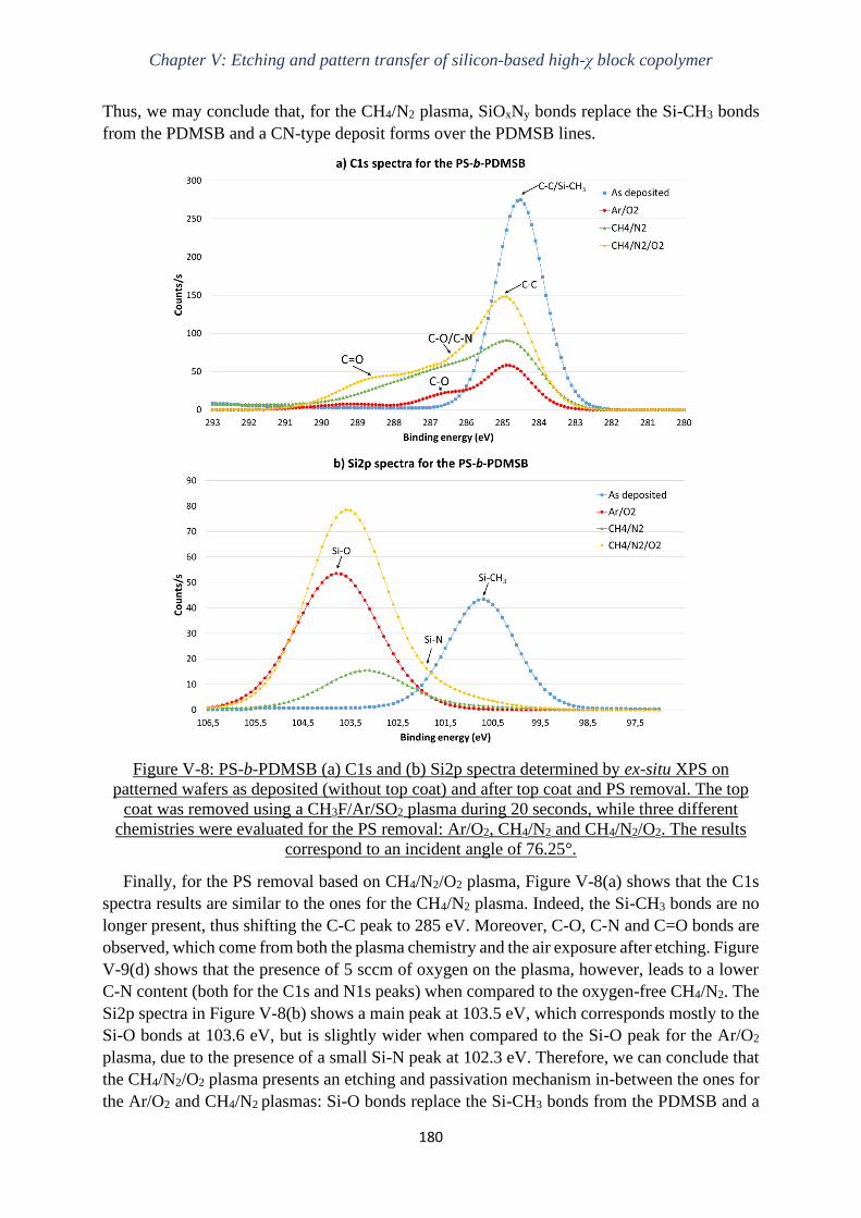
Chapter V: Etching and pattern transfer of silicon-based high-χ block copolymer
180
Thus, we may conclude that, for the CH4/N2 plasma, SiOxNy bonds replace the Si-CH3 bonds
from the PDMSB and a CN-type deposit forms over the PDMSB lines.
Figure V-8: PS-b-PDMSB (a) C1s and (b) Si2p spectra determined by ex-situ XPS on
patterned wafers as deposited (without top coat) and after top coat and PS removal. The top
coat was removed using a CH3F/Ar/SO2 plasma during 20 seconds, while three different
chemistries were evaluated for the PS removal: Ar/O2, CH4/N2 and CH4/N2/O2. The results
correspond to an incident angle of 76.25°.
Finally, for the PS removal based on CH4/N2/O2 plasma, Figure V-8(a) shows that the C1s
spectra results are similar to the ones for the CH4/N2 plasma. Indeed, the Si-CH3 bonds are no
longer present, thus shifting the C-C peak to 285 eV. Moreover, C-O, C-N and C=O bonds are
observed, which come from both the plasma chemistry and the air exposure after etching. Figure
V-9(d) shows that the presence of 5 sccm of oxygen on the plasma, however, leads to a lower
C-N content (both for the C1s and N1s peaks) when compared to the oxygen-free CH4/N2. The
Si2p spectra in Figure V-8(b) shows a main peak at 103.5 eV, which corresponds mostly to the
Si-O bonds at 103.6 eV, but is slightly wider when compared to the Si-O peak for the Ar/O2
plasma, due to the presence of a small Si-N peak at 102.3 eV. Therefore, we can conclude that
the CH4/N2/O2 plasma presents an etching and passivation mechanism in-between the ones for
the Ar/O2 and CH4/N2 plasmas: Si-O bonds replace the Si-CH3 bonds from the PDMSB and a

Chapter V: Etching and pattern transfer of silicon-based high-χ block copolymer
181
CN-type deposit forms over the PDMSB lines. However, this deposit is thinner when compared
to the CH4/N2 plasma probably due to the addition of oxygen to the plasma, which consumes
both the PS and the CN-type deposit.
Figure V-9: PS-b-PDMSB surface composition determined by ex-situ XPS on patterned
wafers (a) as deposited without top coat and (b, c, d) after top coat and PS removal. The top
coat was removed using a CH3F/Ar/SO2 plasma during 20 seconds, while three different
chemistries were evaluated for the PS removal: (b) Ar/O2; (c) CH4/N2; and (d) CH4/N2/O2.
The results correspond to an incident angle of 76.25°.
In this section, three different etching chemistries were evaluated for the PS removal
selectively to the PDSMB: Ar/O2, CH4/N2 and CH4/N2/O2. For the pattern transfer of the
PS-b-PDMSB into the TiN hard mask, we estimated that there should be at least 18 nm of
PDMSB plus neutral layer left after top coat and PS removal, which translates to a
PS:PDMSB selectivity ≥ 2.5. However, the three PS removal chemistries evaluated led to a
maximum selectivity of 1.8, which was not enough for complete pattern transfer.
We then tried increasing the block copolymer’s initial thickness to relax the selectivity
constraints. While it did allow us to increase the available PDMSB budget after top coat
and PS removal, it also led to pattern collapse due to the high aspect ratio of the lines.
Next, XPS analysis were conducted to understand the etching and passivation
mechanisms for the three different plasma approaches. For the Ar/O2 etching, we concluded
that the oxygen consumes the PS by forming volatile COx species while at the same time
transforming the Si-CH3 bonds of the PDMSB into Si-O bonds. For the CH4/N2 plasma,
SiOxNy bonds replace the Si-CH3 bonds from the PDMSB and a CN-type deposit forms
over the PDMSB lines, thus forming a passivation layer and explaining its larger CD when
compared to the other two approaches. Finally, the CH4/N2/O2 plasma presents an etching
and passivation mechanism in-between the ones for the Ar/O2 and CH4/N2 plasmas: Si-O
bonds replace the Si-CH3 bonds from the PDMSB and a CN-type deposit forms over the

Chapter V: Etching and pattern transfer of silicon-based high-χ block copolymer
182
V.3 One step top coat and PS removal selectively to PDMSB
In this section, we propose to evaluate a one-step top coat and PS removal approach which
consists of removing the top coat and the PS selectively to the PDMSB in a single plasma
etching step. For that, we have selected both oxidizing and reducing chemistries that have
already been explored in the two previous chapters as well-known solutions to etch purely
organic materials. We shall start by evaluating two oxygen-based chemistries: the Ar/O2 plasma
detailed in Table V-3 and the CH3F/Ar/SO2 plasma detailed in Table V-1. We then shall
evaluate a reducing H2/N2 plasma, which has already been presented in Chapter III.3.1 as an
alternative for the SOC removal.
Once the best top coat and PS removal approach has been identified, the pattern transfer into
the titanium nitride (TiN), silicon oxide (SiO2) and silicon (Si) underlayers shall be evaluated
in order to confirm this approach’s compatibility with the 18-nm pitch high-χ PS-b-PDMSB.
V.3.1 Comparison between oxidizing and reducing plasma chemistries for
top coat and PS removal
V.3.1.1 Top coat and PS removal with two different oxidizing plasmas
Both the Ar/O2 and CH3F/Ar/SO2 plasmas are applied to the PS-b-PDMSB patterned wafers
with the complete stack from Figure V-1 during 50 seconds and the results are presented in
Figure V-10. For the Ar/O2 plasma, the cross-section SEM image in Figure V-10(a) shows that
there is only around 9.6 nm of PDMSB and neutral layer left after etching, which is not enough
for pattern transfer. Moreover, the top-view SEM image shows some spots where the lines have
been interrupted and the CD is apparently smaller. This is reminiscent of the results obtained
during top coat removal with the Ar/O2 plasma with smaller ratio presented in Figure V-4. Thus,
it could be further indication of a non-homogeneous top coat/PS-b-PDMSB interface. Varying
the etching time or Ar/O2 ratio did not eliminate these defects. These results indicate that the
one-step oxidizing approach using an Ar/O2 plasma is not adapted to this PS-b-PDMSB stack.
For the top coat and PS removal using the CH3F/Ar/SO2 plasma, both top-view and cross-
section SEM images presented in Figure V-10(b) indicate a significant increase in the CD of
the PDMSB lines. It can be explained by the presence of CH3F and SO2 as passivating agents
for the PDMSB, thus forming a passivation layer on the sidewalls of the PDMSB lines and
effectively increasing their CD. This probably leads to the very low selectivity between PS and
PDMSB, which present almost the same thickness after 50 seconds of etching according to the
cross-section SEM in Figure V-10(b). Therefore, the CH3F/Ar/SO2 plasma is not adapted to the
one-step top coat and PS removal approach.
PDMSB lines. However, this deposit is thinner when compared to the CH4/N2 plasma
probably due to the addition of oxygen to the plasma, which consumes both the PS and the
CN-type deposit.
Therefore, none of these plasma processes are compatible with the 18-nm pitch high-χ
PS-b-PDMSB and a new approach that allows for higher PS:PDMSB selectivity without
pattern collapse must be developed.

Chapter V: Etching and pattern transfer of silicon-based high-χ block copolymer
183
Furthermore, the formation of a thicker TiOx layer on the surface of the TiN hard mask using
the oxidizing plasma may induce some difficulties during pattern transfer due to the limited
PDMSB budget available. Therefore, we decided to investigate a reducing plasma based on
H2/N2, which has been shown in Chapter III.3 to etch organic layers with good selectivity to
silicon-containing materials without further modification of TiN hard mask composition.
Figure V-10: Top-view and cross-section SEM images for the PS-b-PDMSB block copolymer
after top coat and PS removal with (a) Ar/O2 or (b) CH3F/Ar/SO2 during 50 seconds.
V.3.1.2 Top coat and PS removal with a reducing plasma
The reducing approach based on H2/N2 is evaluated on a FLEX CFE® capacitively coupled
plasma (CCP) reactor, which has been detailed in Chapter II.2.1.1, due to the H2 not being
available in the ICP reactor. The details of the plasma parameters are presented in Table V-4.
The top coat and PS etch rates on blanket wafers are 5.5 and 2.0 nm/s, respectively. Thus,
etching times varying from 10 to 30 seconds have been applied on patterned wafers in order to
find the best etch durations on PS-b-PDMSB films.
Table V-4: Plasma parameters for the H2/N2 plasma evaluated for top coat and PS removal.
Chemistry Pressure (mTorr) RF 2MHz (W) RF 27MHz (W) Flow (sccm)
H2/N2 160 0 1000 150/500

Chapter V: Etching and pattern transfer of silicon-based high-χ block copolymer
184
The top-view and cross-section SEM images after top coat and PS removal for the studied
etching times can be found in Figure V-11. After 10 seconds, Figure V-11(a) shows that the top
coat has been completely removed and that around 6 nm of PS have been etched, while the
PDMSB is not consumed.
Figure V-11: Top-view and cross-section SEM images of PS-b-PDMSB block copolymer
after top coat and PS removal using H2/N2 with ratio 150/500 for: (a) 10 seconds; (b) 20
seconds; and (c) 30 seconds.
After 20 seconds, Figure V-11(b) indicates that the PS has also been completely removed
and around 23 nm of PDMSB remain, which means a PS:PDMSB minimum selectivity of 4.3.
Indeed, since the PS has been completely removed, it is possible that the PS:PDMSB selectivity

Chapter V: Etching and pattern transfer of silicon-based high-χ block copolymer
185
is greater than 4.3 for shorter etching durations. However, some collapsing of the PDMSB lines
can be observed in the cross-section image in Figure V-11(b), probably due to the high aspect
ratio of the lines, which is around 2.5 due to the small CD of 9 nm.
Finally, after 30 seconds, based on Figure V-11(c), we observe that the PDMSB presents an
average thickness of 18 nm while the PS has been completely removed, translating to a
PS:PDMSB selectivity of 2.5. No pattern collapse is observed after 30 seconds due to the lower
aspect ratio of 2. Moreover, the line patterns after the reducing plasma present an anisotropic
profile and a CD of approximately 10 nm, which means a CD bias of 1 nm when compared to
the as deposited material. However, there is some bridge formation between the lines, which
has already been observed for such small and dense pitch in Chapter IV and has been attributed
to intensive sidewalls passivation and to a species confinement effect accentuated by the small
18-nm pitch [Gusmão 2020].
Therefore, 30 seconds has been selected as the etching duration of reference for the H2/N2
plasma with ratio 150/500 since it is able to obtain the minimum desired PS:PDMSB selectivity
of 2.5 without leading to pattern collapse due to the high aspect ratio of the PDMSB lines.
In order to understand the role of the H2 and N2 on the top coat and PS-b-PDMSB etching
and passivation mechanisms, the gas ratio has been varied while the other plasma parameters
remained the same as the ones presented in Table V-4. The top-view and cross-section SEM
images after top coat and PS removal during 30 seconds are presented in Figure V-12 for the
following H2/N2 flow: 150/50, 150/150, 150/300 and 0/500 (indicated as N2 only). The results
for H2/N2 150/500 have already been presented in Figure V-11(c). The estimated remaining PS
and PDMSB thickness as well as the calculated PS:PDMSB selectivity for each H2/N2 ratio can
be found in Table V-5. Once again, it should be noticed that, since the PS has been completely
removed, the PS:PDMSB selectivity presented corresponds to the minimum value and could be
greater for shorter etching durations. As we can see, the lower the N2 content, the lower the
PS:PDMSB selectivity, thus indicating that N2 plays an important role on PDMSB passivation
and protection.
Table V-5. Estimated remaining PS and PDMSB thickness as well as the calculated minimum
PS:PDMSB selectivity for each H2/N2 ratio. These values were obtained by averaging the
measured values on the SEM images presented in Figures V-11 and V-12.
H2/N2 flow
(sccm)
PS remaining
(nm)
PDMSB remaining
(nm) PS:PDMSB Selectivity
150/50 0 12.7 1.7
150/150 0 16.3 2.2
150/300 0 16.7 2.3
150/500 0 18.0 2.5
0/500 21.6 21.6 1.0
Figure V-12(a) shows the results for H2/N2 150/50, which has the lower N2 content and lower
PS:PDMSB selectivity (1.7) when compared to the other ratios. It should be noticed that no

Chapter V: Etching and pattern transfer of silicon-based high-χ block copolymer
186
bridges are observed on the top-view SEM image, probably because this ratio is less passivating
and has a smaller CD of around 8 nm. A few lines have collapsed, which might be related to
the smaller CD as well as the slight difference in CD between the top and the bottom of the line
that is shown in the cross-section SEM image.
This difference in CD between top and bottom of the line pattern is even more significant
for the ratio 1.0 (150/150), presented in Figure V-12(b). The CD different corresponds to 3 nm,
which also explains the many collapsing lines visible in the top-view SEM image. The bigger
gap in CD might be caused by the combination of two simultaneous phenomena. First, the larger
CD observed on top of the line is probably due to the higher N2 content, which preferably
passivates the top sidewall. Second, the smaller bottom CD may correspond to the lateral
etching of the neutral layer under the PDMSB block, since this layer is purely organic and
etches faster than the silicon-containing PDMSB.
As we observe the two next H2/N2 ratios – 150/300 in Figure V-12(c) and 150/500 in Figure
V-11(c) –, as expected, the greater the N2 content, the better the selectivity since N2 seems to
be the major passivating component of this etching chemistry. For both ratios, the CD difference
between top and bottom of the patterns still exist, but is less significant than the one observed
for the 150/150 ratio and leads to less pattern collapse. The higher N2 content, and therefore
passivation, also leads to the reappearance of bridges, which are visible in the top-view SEM
image in Figure V-12(c).
However, when attempting to etch the top coat and PS with N2 only, we observe in Figure
V-12(d) and Table V-5 that, while the top coat is completely removed, there is no selectivity
between PS and PDMSB. This indicates that H2 is necessary to etch the PS selectively to the
PDMSB.
Therefore, the 150/500 sccm is the most interesting ratio in terms of PS:PDMSB selectivity
(2.5) while 150/50 sccm presents as an advantage the absence of bridging on top of the PDMSB
lines. Both ratios present a slight pattern collapse due to the high aspect ratio of the lines. They
shall be evaluated for pattern transfer into the titanium nitride hard mask in section V.3.3.1.

Chapter V: Etching and pattern transfer of silicon-based high-χ block copolymer
187
Figure V-12: Top-view and cross-section SEM images of PS-b-PDMSB block copolymer
after top coat and PS removal using H2/N2 with different ratios for 30 seconds: (a) 150/50
sccm; (b) 150/150 sccm; (c) 150/300 sccm; and (d) only N2 (500 sccm).

Chapter V: Etching and pattern transfer of silicon-based high-χ block copolymer
188
V.3.2 Understanding the etching and passivation mechanisms
In order to understand the etching and passivation mechanisms involved in the top coat and
PS removal, ex-situ XPS analysis were carried out on blanket top coat and PS homopolymers
before and after etching with the H2/N2 plasma with ratio 150/500. The results are shown in
Figures V-13 and V-14. Figure V-13 presents the atomic percentage for each element in the
different samples while Figure V-14 presents the evolution of the C1s and N1s spectra for the
top coat and PS before and after etching.
The surface composition for the as deposited top coat and PS has already been detailed in
section V.1. The PS homopolymer C1s spectra presented in Figure V-14(b) shows two peaks:
one at 284.8 eV, assigned to C-C/C=C, ant the other at 291.5 eV, identified as pi→pi*. The as
deposited top coat consists of a poly(2,2,2-trifluoroethylmethacrylate-r-glycidylmethacrylate-
r-2-hydroxyethylmethacrylate) statistical terpolymer. The C1s spectra for the as deposited top
coat in Figure V-14(a) presents four different peaks: one at 285.0 eV, identified as C-
In this section, a one-step top coat and PS removal approach has been evaluated with
three different plasma chemistries.
The Ar/O2 plasma presented low PS:PDMSB selectivity and, in some spots, the PDMSB
lines were interrupted and presented smaller CD, which could be further indication of a non-
homogeneous top coat/PS-b-PDMSB interface. The Ar/O2 plasma was therefore considered
not appropriate for the one-step top coat and PS removal.
The CH3F/Ar/SO2 plasma led to a significant increase in the CD of the PDMSB lines,
which was explained by the presence of CH3F and SO2 as passivating agents, thus forming
a passivation layer on the sidewalls of the PDMSB lines and increasing their CD. As a
consequence of the very low PS:PDMSB selectivity due to too much passivation, the
CH3F/Ar/SO2 plasma was also not adapted to the one-step top coat and PS removal.
We then decided to evaluate a reducing top coat and PS removal approach based on
H2/N2 plasma, which led to good PS:PDMSB selectivity and lines profile. By varying the
etching duration, we observed that for shorter etching times (20 seconds), even though the
PS was completely removed and the PS:PDMSB selectivity was good (4.3), the high aspect
ratio of the lines (2.5) led to pattern collapse. Therefore, a longer etching duration of 30
seconds, despite leading to lower PS:PDMSB selectivity (2.5), was selected as the reference
etching time due to the slightly lower aspect ratio of the lines, thus avoiding pattern collapse.
Next, we evaluated the impact of gas ratio variation. On one hand, with lower N2 content
(50 sccm instead of 500 sccm), even though lower PS:PDMSB selectivity was obtained
when compared to the process of reference, there was no bridge formation. On the other
hand, when only N2 is applied to the top coat and PS removal, there is an etch stop. These
results indicate that N2 is the main passivating agent in the plasma, while H2 is the main
etching agent.
Therefore, the 150/500 sccm is the most interesting ratio in terms of PS:PDMSB
selectivity (2.5) while 150/50 sccm presents as an advantage the absence of bridging on top
of the PDMSB lines. Both ratios present a slight pattern collapse due to the high aspect ratio
of the lines. They shall be evaluated for pattern transfer into the titanium nitride hard mask
in a later section.

Chapter V: Etching and pattern transfer of silicon-based high-χ block copolymer
189
C/CHCOOH, which represents both the carbon at CH2 and CH3 bonds (at 284.7 eV) and the
carbon from the acrylate compounds (at 285.7 eV). The second peak appears at 286.5 eV and
represents the carbon in the methyl ester (C-O) bonds. The third one, at 288.8 eV, corresponds
to the carbon in the carboxyl group (C=O). Finally, the fourth one, at 292.7 eV, corresponds to
carbon bound to three fluorine atoms (CF3).
Figures V-13 and V-14 also present the XPS results after etching these materials with H2/N2
plasma. For both materials, a C-N peak appears at 399 eV on the N1s spectra in Figure V-14(c)
and at 286 eV on the C1s spectra – in which, due to spectral resolution, it cannot be
differentiated from C-O (286.5 eV) bonds and is thus fitted together as C-O/C-N in Figures V-
14(a) and (b) [Beamson 1992]. For the PS, this C-N bond formation has already been observed
with CH4/N2 plasma in Chapter IV.3.3.1 and indicates that a CN-type deposit forms on the PS
surface. This CNx layer then probably reacts with the hydrogen in the plasma to form HCN as
a volatile product.
As for the top coat after H2/N2 etching, represented in Figures V-13(b) and V-14(a), a
decrease in percentage of CF3 and C-O simple and double bonds is observed, indicating that
they are preferentially etched by the reactive species present in the H2/N2 plasma. The loss of
C-O and C=O bonds is characteristic of methacrylate-based polymers etching and similar to
what is observed for PMMA etching with CH4/N2 in Chapter IV.3.3.1, as expected given that
both materials present similar characteristic groups in their composition.
Figure V-13: Surface composition of (a, b) Top coat and (c, d) PS homopolymer determined
by ex-situ XPS with an incident angle of 23.75° (a, c) before and (b, d) after etching with
H2/N2 ratio 150/500 for 5 seconds.

Chapter V: Etching and pattern transfer of silicon-based high-χ block copolymer
190
Figure V-14: (a, b) C1s and (c) N1s spectra for (a, c) Top coat and (b, c) hPS determined by
ex-situ XPS with an incident angle of 23.75° before and after etching with H2/N2 ratio
150/500 for 5 seconds.
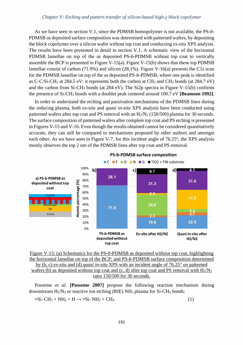
Chapter V: Etching and pattern transfer of silicon-based high-χ block copolymer
191
As we have seen in section V.1, since the PDMSB homopolymer is not available, the PS-b-
PDMSB as deposited surface composition was determined with patterned wafers, by depositing
the block copolymer over a silicon wafer without top coat and conducting ex-situ XPS analysis.
The results have been presented in detail in section V.1. A schematic view of the horizontal
PDMSB lamellae on top of the as deposited PS-b-PDMSB without top coat to vertically
assemble the BCP is presented in Figure V-15(a). Figure V-15(b) shows that these top PDMSB
lamellae consist of carbon (71.9%) and silicon (28.1%). Figure V-16(a) presents the C1s scan
for the PDMSB lamellae on top of the as deposited PS-b-PDMSB, where one peak is identified
as C-C/Si-CH3 at 284.5 eV: it represents both the carbon at CH2 and CH3 bonds (at 284.7 eV)
and the carbon from Si-CH3 bonds (at 284 eV). The Si2p spectra in Figure V-15(b) confirms
the presence of Si-CH3 bonds with a doublet peak centered around 100.7 eV [Beamson 1992].
In order to understand the etching and passivation mechanisms of the PDMSB lines during
the reducing plasma, both ex-situ and quasi in-situ XPS analysis have been conducted using
patterned wafers after top coat and PS removal with an H2/N2 (150/500) plasma for 30 seconds.
The surface composition of patterned wafers after complete top coat and PS etching is presented
in Figures V-15 and V-16. Even though the results obtained cannot be considered quantitatively
accurate, they can still be compared to mechanisms proposed by other authors and amongst
each other. As we have seen in Figure V-7, for this incident angle of 76.25°, the XPS analysis
mostly observes the top 2 nm of the PDMSB lines after top coat and PS removal.
Figure V-15: (a) Schematics for the PS-b-PDMSB as deposited without top coat, highlighting
the horizontal lamellae on top of the BCP; and PS-b-PDMSB surface composition determined
by (b, c) ex-situ and (d) quasi in-situ XPS with an incident angle of 76.25° on patterned
wafers (b) as deposited without top coat and (c, d) after top coat and PS removal with H2/N2
ratio 150/500 for 30 seconds.
Posseme et al. [Posseme 2007] propose the following reaction mechanism during
downstream H2/N2 or reactive ion etching (RIE) NH3 plasma for Si-CH3 bonds:
≡Si–CH3 + NH2 + H → ≡Si–NH2 + CH4 (1)

Chapter V: Etching and pattern transfer of silicon-based high-χ block copolymer
192
For our PDMSB lines, the presence of Si-N bonds after top coat and PS removal using H2/N2
plasma is confirmed by the quasi in-situ XPS analysis. Indeed, Figure V-16(b) presents the Si2p
spectra after etching, which shows that the Si-CH3 peak is no longer present and a new doublet
peak at 102.3 eV (Si2p3/2 at 102 eV and Si2p1/2 at 102.6 eV), representing Si-N bonds, appears
[Beamson 1992]. Moreover, Figure V-16(c) also confirms the presence of the N-Si peak on the
N1s spectra, which appears at a binding energy of 398.5 eV [Ingo 1989]. These results indicate
that the Si-CH3 bonds in PDMSB are probably turned into Si-NH2 during top coat and PS
removal, as proposed in reaction 1.
It is also important to notice that the oxygen and nitrogen atomic percentages presented in
Figures V-15(c) and V-15(d) are the only ones that present a significant variation between quasi
in-situ and ex-situ XPS analysis. Indeed, their values are almost inverted: for the quasi in-situ
XPS, there is around 32% of nitrogen and 5% of oxygen, while for the ex-situ XPS, there is
approximately 35% of oxygen and 2% of nitrogen. This difference can be explained by the
reaction of the Si-NH2 bonds with water molecules when the wafer is exposed to the
atmosphere. The Si-NH2 bonds are replaced by Si–OH bonds, according to the reaction:
≡Si–NH2 + H2O → ≡Si–OH + NH3 (2)
Figure V-16: (a) C1s, (b) Si2p, (c) N1s and (d) O1s spectra determined by ex-situ and quasi
in-situ XPS with an incident angle of 76.25° for the as deposited PS-b-PDMSB (without top
coat) and for the PDMSB lines after top coat and PS removal with H2/N2 ratio 150/500 for 30
seconds.
This reaction is confirmed by the XPS analysis for the ex-situ samples. Figure V-16(b) shows
that the Si-N peak that was present for the quasi in-situ sample has been shifted to a higher
binding energy of 103.6 eV, which is characteristic of the doublet peak for the Si-O bonds
(Si2p3/2 at 103.3 eV and Si2p1/2 at 103.9 eV). Furthermore, the O1s spectra presented in Figure
V-16(d) shows the presence of an O-Si peak at 533 eV [Beamson 1992], thus confirming that
Si-N bonds are replaced by Si-O bonds after air exposure. Also according to Posseme et al.,

Chapter V: Etching and pattern transfer of silicon-based high-χ block copolymer
193
these different reactions lead to the formation of a modified passivation layer composed of
SiOxNyHz, which is denser and carbon depleted [Posseme 2007]. This layer is observed for the
PDMSB according to quasi in-situ XPS analysis in Figure V-16(d), which presents a peak at
532.4 eV that corresponds to Si-O-N bonds [Bois 1996].
In order to minimize the oxidation of the TiN surface after top coat and PS removal, all
experiments of pattern transfer into the TiN layer that shall be presented in the next section are
conducted without air exposure between the top coat and PS removal step and the TiN etching
step. Therefore, we may conclude that the formation of Si-NH2 and SiOxNyHz over the PDMSB
lines is responsible for their passivation during top coat and PS removal with H2/N2 plasma.
V.3.3 Pattern transfer of the 18-nm pitch high-χ PS-b-PDMSB
V.3.3.1 Pattern transfer into the titanium nitride hard mask
For the pattern transfer of the 18-nm pitch high-χ PS-b-PDMSB into the 18-nm hard mask
(15 nm of TiN and around 3 nm of native titanium oxide, TiOx), we have selected three different
combinations of H2/N2 ratio and etching times to evaluate the impact of high selectivity, aspect
ratio and bridge formation. These combinations are 150/50 sccm during 20 seconds, 150/500
sccm during 20 seconds and 150/500 sccm during 30 seconds. The 150/50 ratio for 20 seconds,
while not shown here, presents a PS:PDMSB selectivity of 3.7 with around 21.9 nm of PDMSB
remaining, as well as a straight line profile with a CD of 8 nm and no bridge formation.
Pattern transfer into the TiN hard mask is conducted in a Kiyo® CX ICP reactor from
LamResearch without air exposure after the top coat and PS removal through H2/N2, in order
to avoid further oxidation of the TiN and PDMSB exposed surfaces. The TiN etching consists
of two steps: a breakthrough (BT) step using Cl2/BCl3 to remove the TiOx on the surface and
In this section, we conducted XPS analysis in order to understand the etching and
passivation mechanisms involved in the top coat and PS removal for the 18-nm pitch high-
χ PS-b-PDMSB.
For the PS homopolymer after top coat and PS removal using H2/N2 (150/500 sccm), a
CN-type deposit was formed on the PS surface. This CNx layer then probably reacted with
the hydrogen in the plasma to form HCN as a volatile product. For the top coat after H2/N2
etching, a decrease in percentage of CF3 and C-O simple and double bonds was observed,
indicating that they were preferentially etched by the reactive species present in the H2/N2
plasma.
Finally, for the PS-b-PDMSB patterned wafers, both ex-situ and quasi in-situ XPS
analysis were conducted. Quasi in-situ analysis indicated that the Si-CH3 bonds in PDMSB
were probably turned into Si-NH2 during top coat and PS removal, while ex-situ analysis
showed that these Si-NH2 bonds reacted with water molecules when the wafer was exposed
to the atmosphere, thus being replaced by Si–OH bonds. Furthermore, these different
reactions led to the formation of a modified layer composed of SiOxNyHz, which is denser
and carbon depleted. Therefore, we concluded that the formation of Si-NH2 and SiOxNyHz
over the PDMSB lines was responsible for their passivation during top coat and PS removal
with H2/N2 plasma.

Chapter V: Etching and pattern transfer of silicon-based high-χ block copolymer
194
initiate the TiN etching. This BT step is followed by a main etch (ME) using Cl2/CH4/N2, which
presents better selectivity to the PDMSB thanks to the presence of CH4 and N2 as passivating
agents. Both steps have been validated for other applications at CEA Leti. The plasma
parameters can be found in Table V-6.
Table V-6. Plasma parameters of the chemistries used for the dry etching of the TiN hard mask.
Plasma Pressure (mTorr) Power (W) Bias (V) Flow (ratio) Time (s)
BT: Cl2/BCl3 8 400 -100 2:1 5
ME: Cl2/CH4/N2 10 350 -200 4:1:3 5
Figure V-17 shows the results for the pattern transfer of the high-χ PS-b-PDMSB into the
TiN hard mask using the three top coat and PS removal conditions evaluated. For H2/N2 with
ratio 150/500 for 20 seconds, which is the condition with higher selectivity, and therefore higher
aspect ratio, we observe from the results in Figure V-17(b) that the line patterns have mostly
collapsed. The cross-section SEM image shows that, because of PDMSB collapse, pattern
transfer into the TiN hard mask is not initiated.
Based on the results presented in Figure V-17(a) for the 150/50 ratio during 20 seconds,
which presents an intermediate PDMSB remaining thickness among the three conditions
studied and no bridge formation, pattern collapse is still observed although in smaller intensity
when compared to the previous condition presented in Figure V-17(b). Pattern transfer into the
TiN hard mask is initiated: the TiOx layer has been opened and around 5 nm of TiN have been
etched. However, pattern collapse probably prevented further TiN etching.
Finally, the best result is obtained with the third condition, H2/N2 with ratio 150/500 for 30
seconds, which is presented in Figure V-17(c). For this combination, the TiOx layer has been
opened and around 10 nm of TiN have been etched. Moreover, no pattern collapse is observed.
However, the PDMSB mask has been completely etched, which is confirmed when we extend
the main etch time to 10 seconds (not depicted) instead of 5 seconds and observe that the line
patterns are no longer present because the TiN has been overetched.
These results lead to the conclusion that, while good PS:PDMSB selectivity is desired in
order to conserve enough PDMSB budget to completely transfer the line patterns into the hard
mask, mechanical stability problems cause pattern collapse due to the high aspect ratio of the
lines. Therefore, the smaller CD of the high-χ block copolymer limits the maximum PDMSB
budget allowed for pattern transfer, which in its turn limits the TiN thickness that can be etched
using this block copolymer as a mask. Herein we are able to transfer 18-nm pitch PDMSB lines
into a TiN thickness of 10 nm.
Further investigation into solutions to improve the block copolymer’s mechanical stability
would be necessary in order to increase the etching process window for the TiN hard mask.

Chapter V: Etching and pattern transfer of silicon-based high-χ block copolymer
195
Figure V-17: Top-view and cross-section SEM images of the pattern transfer of high-χ PS-b-
PDMSB into the TiN hard mask using three different conditions for the top coat and PS
removal with H2/N2: (a) 150/50 sccm during 20 seconds; (b) 150/500 sccm during 20 seconds;
and (c) 150/500 sccm during 30 seconds.
V.3.3.2 Pattern transfer into the silicon oxide hard mask and silicon bulk
Due to the limits imposed by the PDMSB budget to the TiN etching, we decided to adapt
the stack studied by replacing the TiN hard mask by a 10-nm SiO2 hard mask. Just as it was
shown in Chapter IV, the goal is to demonstrate a proof-of-concept pattern transfer for this
high-χ BCP. The top coat and PS are removed using the best result from the previous section:

Chapter V: Etching and pattern transfer of silicon-based high-χ block copolymer
196
H2/N2 with ratio 150/500 for 30 seconds. The SiO2 etching is conducted in the same CCP reactor
as the top coat and PS removal, with the following parameters: CF4/H2/Ar with ratio 3.6:1:14,
pressure of 50 mTorr, RF 2 MHz at 600W and RF 27 MHz at 300W for 7 seconds. Next, the
silicon is partially etched in the Kiyo® CX ICP reactor without air exposure in between. The
plasma parameters for Si etching are: CH2F2/SF6/N2/He with ratio 3:2:3:7, pressure of 5 mTorr,
RF power at 450W and RF bias at -70V for 11 seconds. Both plasma chemistries have been
previously validated for other applications within CEA Leti.
After SiO2 etching, Figure V-18(a) shows no pattern collapse, however some bridges are
present, probably originated from the top coat and PS removal step. The cross-section SEM
image shows that the pattern transfer into the 10-nm SiO2 layer is complete and that there are
around 7 nm of PDMSB left. Moreover, the lines present a good, straight profile and a CD
slightly larger than the initial one (10 nm instead of 9 nm).
Figure V-18: Top-view and cross-section SEM images of the pattern transfer of high-χ PS-b-
PDMSB (a) into the SiO2 hard mask and (b) Si bulk using H2/N2 150/500 during 30 seconds
for the top coat and PS removal.
After partially etching the Si bulk, the top-view and cross-section SEM images presented in
Figure V-18(b) show that the line pattern has been transferred into 13 nm of Si and there are
approximately 10 nm of SiO2 left, thus indicating the possibility to obtain very high aspect ratio
silicon features with a plasma etching with good Si:SiO2 selectivity. Moreover, the good
mechanical stability of silicon should prevent pattern collapse. The CD bias between the silicon
oxide and silicon bulk etching steps is 2 nm and the final CD is around 8 nm, thus respecting

Chapter V: Etching and pattern transfer of silicon-based high-χ block copolymer
197
the CD bias ≤ 2 nm condition. Some bridges are still present, having been transferred from the
previous etching steps. Furthermore, no pattern collapse is observed, though a slight wiggling
of the lines may be observed with the top-view SEM image in Figure V-18(b). The silicon
etching step could be optimized in order to better conserve the CD, possibly avoiding the
wiggling effect.
Therefore, we demonstrate the pattern transfer of an 18-nm pitch high-χ silicon-containing
block copolymer into a 23-nm thick SiO2 and silicon stack using a reducing H2/N2 plasma
etching for top coat and PS removal.
V.4 Conclusions
Throughout this chapter, we investigated two different approaches for the top coat and PS
removal selectively to the PDMSB. The first one was based on a top coat removal selectively
to the block copolymer, followed by the PS removal selectively to the PDMSB in a separate
step. The second one, on the other hand, consisted of a top coat and PS removal in a single step.
For the two-step approach, two oxygen-containing plasma etching were selected to
investigate the top coat removal: Ar/O2 and CH3F/Ar/SO2. When the Ar/O2 plasma was applied
to the patterned wafers with the complete PS-b-PDMSB and top coat stack, we observed some
brighter spots where no line/space patterns were visible. Moreover, where the bright spots were
not present, the lines were mostly interrupted and presented a smaller CD. This etch stop of the
top coat in certain areas of the wafer could be explained by the presence of something at the top
coat and BCP interface that does not etch in Ar/O2 plasma (for example, a non-homogeneous
PDMSB interface or non-volatile etching by-products). On the other hand, when using the
CH3F/Ar/SO2 plasma during 20 seconds, the top coat layer was completely removed without
In this section, we started by evaluating the pattern transfer of the high-χ PS-b-PDMSB
into the TiN hard mask. Three different top coat and PS removal conditions were explored
and the results led to the conclusion that, while good PS:PDMSB selectivity is desired in
order to conserve enough PDMSB budget to completely transfer the line patterns into the
hard mask, mechanical stability problems caused pattern collapse due to the high aspect
ratio of the lines. Therefore, the smaller CD of the high-χ block copolymer limited the
maximum PDMSB budget allowed for pattern transfer, which in turn limited the TiN
thickness that could be etched using this block copolymer as a mask. Nevertheless, we were
able to transfer the 18-nm pitch PDMSB lines into a TiN thickness of 10 nm, which could
allow for pattern transfer into other subjacent layers using the 10 nm of TiN as hard mask.
Furthermore, a proof of concept for the pattern transfer into a 10-nm SiO2 hard mask
was also validated. After complete pattern transfer into the silicon oxide layer with good
profile and CD, there were around 7 nm of PDMSB left. We then demonstrated the partial
pattern transfer into approximately 13 nm of the silicon bulk layer while conserving the
SiO2 hard mask, thus indicating the possibility to obtain very high aspect ratio silicon
features with a plasma etching with good Si:SiO2 selectivity. Therefore, we validated the
pattern transfer of an 18-nm pitch high-χ silicon-containing block copolymer into a 23-nm
thick SiO2 and silicon stack using a reducing H2/N2 plasma etching for top coat and PS
removal.

Chapter V: Etching and pattern transfer of silicon-based high-χ block copolymer
198
significantly etching the block copolymer. Therefore, this process was selected as the process
of reference for the top coat removal.
Once the top coat removal process was validated, three different etching chemistries were
evaluated for the PS removal selectively to the PDSMB: Ar/O2, CH4/N2 and CH4/N2/O2. For
the pattern transfer of the PS-b-PDMSB into the TiN hard mask, we estimated that a
PS:PDMSB selectivity ≥ 2.5 was necessary. However, the three PS removal chemistries
evaluated led to a maximum selectivity of 1.8, which was not enough for complete pattern
transfer. We then tried increasing the block copolymer’s initial thickness to relax the selectivity
constraints. While it did allow us to increase the available PDMSB budget after top coat and
PS removal, it also led to pattern collapse due to the high aspect ratio of the lines. Therefore,
none of these plasma processes were compatible with the 18-nm pitch high-χ PS-b-PDMSB.
We then explored the one-step top coat and PS removal approach with three different plasma
chemistries. The Ar/O2 plasma presented low PS:PDMSB selectivity and, in some spots, the
PDMSB lines were interrupted and presented smaller CD, which could be further indication of
a non-homogeneous top coat/PS-b-PDMSB interface. The Ar/O2 plasma was therefore
considered not appropriate for the one-step top coat and PS removal. The CH3F/Ar/SO2 plasma
led to a significant increase in the CD of the PDMSB lines, which was explained by the presence
of CH3F and SO2 as passivating agents, thus forming a passivation layer on the sidewalls of the
PDMSB lines and increasing their CD. As a consequence of the very low PS:PDMSB
selectivity due to too much passivation, the CH3F/Ar/SO2 plasma was also not adapted to the
one-step top coat and PS removal.
We then investigated a reducing plasma based on H2/N2 to etch the organic phase (PS) of
the block copolymer with good selectivity to the silicon-containing phase (PDMSB) while
avoiding further oxidation of the titanium nitride hard mask. For a H2/N2 ratio of 150/500, after
20 seconds the PS was completely removed with a PS:PDMSB selectivity of 4.3, but some
pattern collapse was observed due to the high aspect ratio of the lines. Prolonging the etching
time to 30 seconds led to a PDMSB remaining thickness of 18 nm (PS:PDMSB selectivity =
2.5) and no pattern collapse was observed due to the lower aspect ratio of 2. However, some
bridges were formed between the lines, which was attributed to intensive sidewalls passivation
and to a species confinement effect accentuated by the small and dense pitch.
The gas ratio was varied in order to understand the role of the H2 and N2 on the top coat and
PS-b-PDMSB etching and passivation mechanisms. We showed that higher N2 content leads to
higher selectivity but also more bridge formation, indicating that N2 is the main passivating
agent in this reducing plasma. Higher H2 content, on the other hand, led to lower selectivity and
to an undercutting of the lines due to the neutral layer’s lateral etching. However, when
attempting to etch the top coat and PS with N2 only, while the top coat was completely removed,
there was no selectivity between PS and PDMSB. This indicated that H2 is necessary to etch
the PS selectively to the PDMSB.
Ex-situ and quasi in-situ XPS analysis were conducted to further understand the etching and
passivation mechanisms. After etching, the top coat presented a loss of C-O simple and double
bonds as well as CF3 bonds, which is characteristic of other methacrylate-based polymers
etching, such as PMMA. As for PS, the formation of a CNx layer was observed on the surface,
which was then removed by hydrogen reactive species by forming HCN as a volatile by-

Chapter V: Etching and pattern transfer of silicon-based high-χ block copolymer
199
product. As for the PDMSB, the formation of Si-NH2 and SiOxNyHz was responsible for the
PDMSB passivation during top coat and PS removal with H2/N2 plasma.
Finally, we proceeded to the pattern transfer of the PDMSB lines into 10 nm of the 18-nm
TiN hard mask. The results led to the conclusion that, while good PS:PDMSB selectivity is
desired in order to conserve enough PDMSB budget to completely transfer the line patterns into
the hard mask, mechanical stability problems caused pattern collapse due to the high aspect
ratio of the lines. Therefore, the smaller CD of the high-χ block copolymer limited the
maximum PDMSB budget allowed for pattern transfer (and therefore the PS:PDMSB
selectivity), which in its turn limited the TiN thickness that could be etched using this block
copolymer as a mask. We then replaced the TiN hard mask by a 10-nm SiO2 hard mask for a
proof of concept of pattern transfer. After complete pattern transfer into the silicon oxide layer
with good profile and CD, there were around 7 nm of PDMSB left. Next, we demonstrated the
partial pattern transfer into approximately 13 nm of the silicon bulk layer while conserving the
SiO2 hard mask, thus indicating the possibility to obtain very high aspect ratio silicon features
with a plasma etching with good Si:SiO2 selectivity. Therefore, we validated the pattern transfer
of an 18-nm pitch high-χ silicon-containing block copolymer into a 23-nm thick SiO2 and
silicon stack using a reducing H2/N2 plasma etching for top coat and PS removal.

200

201
CHAPTER VI: CONCLUSION AND PERSPECTIVES

Chapter VI: Conclusion and perspectives
202
VI. CONCLUSION AND PERSPECTIVES
Chapter I presented the state-of-the-art of the various techniques used for pattern
miniaturization in the transistor fabrication process. For decades, optical lithography has been
used, but resolution limits prevent this technique from being considered for patterns with critical
dimensions inferior to 20 nm. Therefore, to continue pattern scaling, new lithography
techniques have been explored throughout the years, such as spacer patterning (or SADP),
Extreme Ultraviolet (EUV), Nanoimprint (NIL) and others. Of the various lithography
techniques that emerged, the Directed Self-Assembly (DSA) of block copolymers was the one
retained for this PhD thesis, namely for line/space applications.
In the introduction chapter, we have also seen that one of the critical steps for the integration
of DSA in the microelectronics industry is the alignment of the block copolymers in long range
distance, that is, obtaining straight, narrow lines throughout the wafer. To do so, two main
techniques were developed, known as grapho-epitaxy and chemo-epitaxy. The chapter detailed
some of the different alignment flows developed these last couple decades. At CEA Leti, the
main integration flow studied is the “ACE” (for Arkema-CEA) chemo-epitaxy flow. This
process aims to align high-χ block copolymers using spacer lithography to form very narrow
guiding lines, thus inducing the block copolymer’s alignment due to chemical affinity
constraints.
Chapter I also introduced the high-χ block copolymers, which present smaller pitch due to
the higher interaction parameter (χ) between the two blocks. Indeed, a higher χ allows us to
reduce the value of the degree of polymerization (N) – and thus also reduce the BCP’s period
(L0) – without violating the condition of the order-disorder transition (χN > 10.5). Moreover,
the increase in χ leads to an increase in repulsion between the blocks, and therefore the domains
are better defined, and present better roughness compared to larger-pitch block copolymers such
as PS-b-PMMA.
We then established the state-of-the-art of another important step in the integration of block
copolymers, which consists of removing one phase of the block copolymer selectively to the
other through to etching, while conserving enough of the remaining block to correctly transfer
the patterns into the subjacent layers.
Therefore, this PhD focused on the etching of both purely organic and silicon-containing
high-χ lamellar block copolymers, having as goal to successfully remove one block and transfer
the line/space patterns into the desired subjacent layers. It also investigated the impact of plasma
etching on the ACE process in order to optimize the flow for a PS-b-PMMA BCP and a future
application with high-χ block copolymers.
Chapter II detailed the characteristics of the different polymeric materials studied
throughout this PhD, namely their composition and deposition parameters. It also presented the
properties of the different etching reactors, both ICP and CCP, used to study the plasma etching
of the high-χ block copolymers; as well as the wet etching tool used for understanding the
interaction between plasma etching, the hard mask and the neutral layer during the ACE chemo-
epitaxy process. Finally, it explained the principle of several characterization tools used during
this thesis to determine the physicochemical and morphological properties of the materials
studied before and after etching, detailing the experimental setup and data analysis.
Chapter III focused on evaluating the impact that the different etching steps of the ACE
flow have on the surface properties (composition and surface energy) of the TiN hard mask,

Chapter VI: Conclusion and perspectives
203
and thus on the final self-assembly of the block copolymer over it. We applied the non-
optimized process of reference to patterned wafers, which led us to realize that different types
of defects could be seen in the top-view image of the block copolymer’s alignment after the
DSA step, such as dark spots and alignment defects. To understand the origin of the defects and
evaluate the hard mask’s capability to align the block copolymer, we studied the effect of the
sequence of etching and deposition steps on the TiN surface and neutral layer adherence using
blanket wafers. We then concluded that the dark spots and alignment defects were caused by a
lift-off phenomenon, confirming the inadequacy of the non-optimized flow to align the BCP.
By investigating the effect of each etching step on the TiN surface, we observed that all of
them induced significant surface energy and composition modifications when compared to the
pristine TiN hard mask. Furthermore, to verify the adherence of the neutral layer to the TiN
surface modified by the different etching steps, the neutral layer thickness was measured before
and after HF wet etching. Ellipsometry measurements showed that the neutral layer is
completely removed for the samples after trilayer etching and SOC removal, which were both
based on SO2/O2/He plasma. Further investigation on the effect of the RF bias and each gas
(SO2, O2 and He) separately showed that the SO2 molecule was the main responsible for this
recipe’s inadequacy to the ACE flow. Thus, our goal was to understand the interaction
mechanisms between the SO2 plasma, the TiN surface, the xNL deposition and the HF wet
etching that led to the lift-off of the neutral layer. Several hypotheses were proposed and the
one retained as the most probable was: SO42− ions interact with the neutral layer’s cross-linking
agent, disrupting its complete cross-linking and allowing the HF to pass through. The HF then
removes the modified TiO2/TiOxSy layer formed on the TiN surface, which reduces the neutral
layer adherence to the TiN hard mask and allows its consequent lift-off.
Finally, we proposed two different alternatives for the SOC removal: replacing the
SO2/O2/He plasma or adding a post-treatment step. To replace the SO2/O2/He, two plasma
chemistries were explored (O2 and H2/N2). The O2 etching modifies the surface composition
and energy of the TiN hard mask, but allows the xNL to be conserved during HF wet etching
and presents several different process windows for patterned wafers. However, due to a
microloading effect on patterned wafers, it does not allow complete SOC removal for smaller
pitch and CDSOC, leading to a hybrid chemo/grapho-epitaxy alignment as a function of the
multiplication factor. The H2/N2 etching conserves the surface energy and composition of the
as deposited TiN, and therefore allows the xNL to resist the HF wet etching. Similarly to the
O2 etching, microloading effects during etching of patterned wafers lead to SOC residues for
smaller patterns and to a hybrid chemo/grapho-epitaxy alignment. While the H2/N2 approach
presents the best defectivity result for a single {CDSOC/pitch} pair, with 0 def/100µm² for a
lithography pitch of 128 nm, it presents fewer process windows compared to O2 etching.
In order to further optimize the block copolymer’s alignment with the ACE flow, the second
approach consisted in a two-step SOC removal: SO2/O2/He plasma followed by the H2/N2
plasma. This approach exhibits the best alignment results when compared to the other
approaches investigated. Indeed, the combination of both plasmas allows for all the
prerequisites to be met: the SOC layer is completely removed, the TiN surface properties are
conserved, the xNL adheres to the TiN surface throughout the HF wet etching step, and the
ACE process is determined mainly by chemo-epitaxy.
Chapter IV focused on the PMMA removal selectively to PS on high-χ modified PS-b-
PMMA films with an 18-nm pitch and 21-nm initial thickness. By characterizing the

Chapter VI: Conclusion and perspectives
204
composition of the modified PS and PMMA homopolymers that compose the modified PS-b-
PMMA block copolymer, we concluded that the modified PS-b-PMMA presents a composition
similar to that of standard PS-b-PMMA. Then, we selected different plasma chemistries and we
evaluated their etch rate, and consequent selectivity, on modified PS and PMMA
homopolymers, therefore selecting two different chemistries that fulfilled our selectivity
requirement: CH3F/Ar/SO2 and CH4/N2.
We then characterized the impact of the modified chemistry, pitch and initial thickness on
the etching of the high-χ modified PS-b-PMMA. When comparing a modified and a standard
PS-b-PMMA BCP with the same pitch and initial thickness, we concluded that, for the same
plasma etching chemistry, the high-χ modified PS-b-PMMA chemistry does not present a
significant impact on the PMMA plasma etching when compared to the standard PS-b-PMMA
block copolymer. However, when comparing the high-χ modified PS-b-PMMA with two
different pitch (18 and 32 nm) and two different initial thicknesses (16 and 36 nm, respectively),
for the high-χ L18 BCP, the same etching chemistries that were validated for larger pitch (32
nm) present different problems that prevent pattern transfer into the SiO2 hard mask for the
smaller-pitch BCP. Therefore, we concluded that the main high-χ L18 PS-b-PMMA plasma
etching challenges come from its small dimensions, namely the pitch and initial thickness.
Different approaches were tested to improve the PMMA:PS selectivity and increase the
remaining PS budget after PMMA removal. Increasing the initial thickness of the high-χ L18
film led to mechanical stability problems and to pattern wiggling due to the high aspect ratio of
the lines, showing that the smaller CD of the high-χ block copolymer limits the maximum initial
thickness allowed for the BCP film in order to avoid pattern wiggling or collapse. We also
varied the CH4/N2 ratio to find a good compromise between etching and carbon passivation.
While for PS and PMMA homopolymers we succeeded in etching the PMMA without
consuming the PS thanks to a CN-type deposition layer formed on the PS surface, the same
could not be applied to the high-χ PS-b-PMMA block copolymer assembled on a free surface.
The results showed that high-χ BCP requires higher selectivity than standard PS-b-PMMA due
to its smaller thickness. Moreover, the CH4/N2 ratio 1:1, while presenting the best PMMA:PS
selectivity without pattern collapse, also presented some bridge formation on top of the lines,
which were probably formed due to intensive sidewalls passivation and to a species
confinement effect accentuated by the small CD (9 nm). We then concluded that the main high-
χ PS-b-PMMA dry etching difficulties come from the trade-off between obtaining high
selectivity and avoiding bridge formation.
The final approach proposed was a mixed wet and dry etching process. The wet PMMA
removal presents infinite selectivity on high-χ modified PS-b-PMMA. The UV exposure with
a dose of 30 mJ/cm² and a wavelength of 172 nm causes the PMMA chains to break by scission
of the C=O and C-O bonds. The IPA rinse then removes the broken PMMA chains without
modifying the PS lines. A dry etching process to open the neutral layer using an Ar/O2 plasma
with high argon content (120/5 sccm) was developed to obtain a highly anisotropic etching and
to conserve more PS budget. With this mixed wet and dry etching approach, the complete
pattern transfer of an 18-nm pitch high-χ organic block copolymer into the 10-nm SiO2 hard
mask and around 14 nm of the silicon bulk layer was validated with CD bias ~ 2 nm.
Chapter V focused on the top coat and PS removal selectively to PDMSB on high-χ silicon-
containing PS-b-PDMSB films with an 18-nm pitch and 30-nm initial thickness. To do so, two
different approaches were investigated and the second one, which consisted of a top coat and

Chapter VI: Conclusion and perspectives
205
PS removal in a single step, was selected as the best result. This approach was based on a
reducing H2/N2 plasma to etch the organic phase (PS) of the block copolymer with good
selectivity to the silicon-containing phase (PDMSB) while avoiding further oxidation of the
titanium nitride hard mask. For a H2/N2 ratio of 150/500, after 20 seconds, the PS was
completely removed with a PS:PDMSB selectivity of 4.3, but some pattern collapse was
observed due to the high aspect ratio of the lines. Prolonging the etching time to 30 seconds led
to a PDMSB remaining thickness of 18 nm (PS:PDMSB selectivity = 2.5) and no pattern
collapse was observed due to the lower aspect ratio of 2. However, some bridges were formed
between the lines, which was attributed to intensive sidewalls passivation and to a species
confinement effect accentuated by the small and dense pitch, as seen in Chapter IV for the high-
χ PS-b-PMMA.
The gas ratio was varied in order to understand the role of the H2 and N2 on the top coat and
PS-b-PDMSB etching and passivation mechanisms. We showed that higher N2 content leads to
higher selectivity but also more bridge formation, indicating that N2 is the main passivating
agent in this reducing plasma. Higher H2 content, on the other hand, led to lower selectivity and
to an undercutting of the lines due to the neutral layer’s lateral etching. However, when
attempting to etch the top coat and PS with N2 only, while the top coat was completely removed,
there was no selectivity between PS and PDMSB. This indicated that H2 is necessary to etch
the PS selectively to the PDMSB. Ex-situ and quasi in-situ XPS analysis were conducted to
further understand the etching and passivation mechanisms. After etching, the top coat
presented a loss of C-O, C=O and CF3 bonds, which is characteristic of other methacrylate-
based polymers etching, such as PMMA. As for PS, the formation of a CNx layer was observed
on the surface, which was then removed by hydrogen reactive species by forming HCN as a
volatile by-product. As for the PDMSB, the formation of Si-NH2 and SiOxNyHz was responsible
for the PDMSB passivation during top coat and PS removal with H2/N2 plasma.
Finally, we proceeded to the pattern transfer of the PDMSB lines into 10 nm of the 18-nm
TiN hard mask. The results led to the conclusion that, while good PS:PDMSB selectivity is
desired in order to conserve enough PDMSB budget to completely transfer the line patterns into
the hard mask, mechanical stability problems caused pattern collapse due to the high aspect
ratio of the lines – a difficulty that we also saw for the high-χ PS-b-PMMA in Chapter IV.
Therefore, the smaller CD of the high-χ block copolymer limited the maximum PDMSB budget
allowed for pattern transfer (and therefore the PS:PDMSB selectivity), which in its turn limited
the TiN thickness that could be etched using this block copolymer as a mask. We then replaced
the TiN hard mask by a 10-nm SiO2 hard mask for a proof of concept of pattern transfer. After
complete pattern transfer into the silicon oxide layer with good profile and CD, there were
around 7 nm of PDMSB left. Next, we demonstrated the partial pattern transfer into
approximately 13 nm of the silicon bulk layer while conserving the SiO2 hard mask, thus
indicating the possibility to obtain very high aspect ratio silicon features with a plasma etching
with good Si:SiO2 selectivity. Therefore, we validated the pattern transfer of an 18-nm pitch
high-χ silicon-containing block copolymer into a 23-nm thick SiO2 and silicon stack using a
reducing H2/N2 plasma etching for top coat and PS removal.

Chapter VI: Conclusion and perspectives
206
Perspectives
1) Alignment of high-χ PS-b-PMMA with pitch 18 nm using the optimized ACE
chemo-epitaxy flow.
Now that the ACE process flow has been optimized and presents good alignment and low
defectivity for a standard PS-b-PMMA block copolymer, the goal is to align the high-χ modified
PS-b-PMMA with pitch L0 = 18 nm.
Figure VI-1 shows a first CD-SEM image of the L18 high-χ PS-b-PMMA aligned using the
ACE flow. Since we have shown in Chapter IV that the standard and modified PS-b-PMMA
present similar compositions, the neutral layer and guiding layer used when applying the ACE
flow to the L18 high-χ PS-b-PMMA are the same ones from the standard PS-b-PMMA studied
throughout Chapter III. Therefore, the SOC removal step is well-adapted to the cross-linkable
neutral layer (xNL) used and does not cause its lift-off during HF wet etching. The blocks of
The results obtained with the ACE flow in Chapter III show a good improvement of
alignment and defectivity after the optimization of the SOC removal step. Thus, this thesis
presented the development and optimization of a chemo-epitaxy method more resolving
than those existing to date. Indeed, thanks to the ACE flow, the integration of high-χ block
copolymers with pitch inferior to 20 nm using optical immersion lithography is made
possible.
Two high-χ block copolymers with pitch 18 nm, one purely organic (modified PS-b-
PMMA) and the other silicon-containing (PS-b-PDMSB), were studied in Chapters IV and
V, respectively. The removal of one block selectively to the other led to some similar
conclusions in both cases. First, we have seen that high-χ BCPs demand higher selectively
during block removal due to their lower initial thickness when compared to large-pitch
block copolymers such as standard PS-b-PMMA. However, due to the small CD of these
BCPs (CD ~ 9 nm), high selectivity may lead to mechanical stability problems, which cause
pattern collapse because of the high aspect ratio of the lines. Indeed, a remaining BCP
budget superior to 25 nm, while ideal for complete pattern transfer into the subjacent layers,
also leads to an aspect ratio of the BCP lines superior to 2.5, thus increasing the risk of
pattern collapse. Therefore, the smaller CD of the high-χ block copolymer limits the
maximum BCP budget allowed for pattern transfer, which in turn limits the hard mask
thickness that can be etched using this block copolymer as a mask.
Furthermore, a bridge formation phenomenon on top of the lines was also observed for
more passivating plasma chemistries. They were probably formed due to intensive sidewalls
passivation and to a species confinement effect accentuated by the small CD (9 nm). All of
these results led to the conclusion that the main high-χ block copolymer dry etching
challenges come from the trade-off between obtaining high selectivity, avoiding bridge
formation and avoiding pattern collapse.
Nevertheless, we were able to transfer both 18-nm pitch high-χ block copolymers into a
10-nm SiO2 hard mask. After complete pattern transfer into the silicon oxide layer with
good profile and CD, we then demonstrated the partial pattern transfer into approximately
13 nm of the silicon bulk layer while conserving the SiO2 hard mask, thus indicating the
possibility to obtain high aspect ratio silicon features.

Chapter VI: Conclusion and perspectives
207
L18 are aligned for multiplication factors (MF) 2 and 3. However, Figure VI-1 indicates that
the L18 high-χ BCP presents higher LER and LWR when compared to the results obtained for
the standard L32 PS-b-PMMA in Chapter III. This may be caused by either an aging effect of
the BCP or by the non-optimized spacer CD, which does not correspond to the block
copolymer’s CD (9 nm). Thus, an optimization of the spacer CD and a study of the modified
PS-b-PMMA aging may be necessary to improve the alignment and roughness results.
Furthermore, the software used for measuring the number of defects developed at CEA Leti
– also known as Deboara – must be optimized for the smaller dimensions of the high-χ BCP.
For the moment, the measurement of the number of defects is subject to detection errors that
do not allow the establishment of defectivity maps to determine precise process windows. The
experimental details of the defectivity measurements using the Deboara software can be found
in [Le Pennec 2021].
Figure VI-1: Top-view SEM image of high-χ modified PS-b-PMMA with pitch 18 nm aligned
using the ACE chemo-epitaxy flow.
2) Alignment of high-χ PS-b-PDMSB with pitch 18 nm using the optimized ACE
chemo-epitaxy flow.
The ACE chemo-epitaxy flow can also be used to align the silicon-containing high-χ PS-b-
PDMSB block copolymer. As we have seen in Chapter II, this BCP requires a graftable neutral
layer based on poly(2-ethylhexyl methacrylate) (PEHMA) homopolymer. To verify the neutral
layer’s compatibility with the TiN surface after SOC removal, a study similar to the one
conducted in Chapter III for the PS-b-PMMA cross-linkable neutral layer (xNL) was conducted
for the PEHMA homopolymer.
First, the neutral layer was deposited on the pristine TiN surface to measure its initial
thickness and water contact angle (WCA) using ellipsometry and contact angle measurements,
respectively. The results are presented in Table VI-1: the neutral layer presents an initial
thickness of around 6 nm and a WCA of 92.2° before HF. Then, the neutral layer was deposited
over the TiN surface after SOC removal using either the non-optimized process (SO2/O2/He)
or the optimized process (SO2/O2/He + H2/N2) to compare the results. The measured thickness
and WCA before and after 60 seconds of HF wet etching are presented in Table VI-1 for the
different samples.

Chapter VI: Conclusion and perspectives
208
Table VI-1 shows that, for the TiN after SOC removal with the non-optimized plasma
(SO2/O2/He), the neutral layer is almost completely removed after HF wet etching and the WCA
decreases approximately in half (46.8°). However, for the TiN as deposited and after SOC
removal using the optimized plasma (SO2/O2/He + H2/N2), after HF wet etching there is a slight
reduction of the neutral layer’s thickness of around 2 nm but the water contact angle remains
unchanged (around 92.2°).
Table VI-1. Neutral layer thickness measured by ellipsometry before and after HF wet etching
for 60 seconds when deposited over the TiN surface before and after each etching step, as well
as the water contact angle (WCA) before and after HF.
Before HF 60s After HF 60s
Neutral layer deposited on Thickness
(nm)
WCA (°) Thickness
(nm)
WCA (°)
TiN as deposited 5.9 ± 0.4 92.2 ± 0.3 4.1 ± 0.6 92.5 ± 0.4
TiN after SO2/O2/He 7.0 ± 0.4 92.3 ± 0.4 0.4 ± 0.3 46.8 ± 5.6
TiN after SO2/O2/He + H2/N2 7.1 ± 0.4 92.2 ± 0.2 5.2 ± 0.5 92.2 ± 0.4
CD-SEM images of the neutral layer before and after HF wet etching were also obtained to
verify the presence of lift-off spots. Figure VI-2(a) shows the neutral layer’s surface before HF,
which is completely uniform and free of dark spots. Figures VI-2(b), (c) and (d) represent the
NL surface after 60 seconds of HF wet etching when deposited over the different TiN surfaces.
On one hand, we first notice that Figure VI-2(c), which corresponds to the TiN after SO2/O2/He
plasma, presents many lift-off spots (dark areas), which confirms the results already observed
in Table VI-1. On the other hand, Figures VI-2(b) and (d), which correspond to the TiN as
deposited and after SOC removal using the SO2/O2/He + H2/N2 plasma respectively, present
fewer lift-off spots when compared to Figure VI-2(c), which is expected given the slight
reduction in the neutral layer’s thickness (around 2 nm) observed in Table VI-1 for these two
samples. This thickness reduction observed even for the as deposited TiN – which was not the
case for the cross-linkable neutral layer (xNL) in Chapter III – indicates that the graftable NL
of the PS-b-PDMSB block copolymer may not be fully compatible with the TiN hard mask.
Nevertheless, the next step should be to apply the ACE chemo-epitaxy flow to the PS-b-
PDMSB block copolymer using the graftable PEHMA neutral layer and the optimized SOC
removal plasma. This would allow us to verify if this thickness reduction of 2 nm after HF wet
etching would affect the BCP’s alignment or if the fact that the water contact angle remains
unchanged after HF means the neutral layer retains its ability to align the block copolymer.
If the PEHMA graftable neutral layer cannot provide a good BCP alignment, another
alternative would be to use the top coat layer, which is composed of a poly(2,2,2-
trifluoroethylmethacrylate-r-glycidylmethacrylate-r-2-hydroxyethylmethacrylate) statistical
terpolymer. Since this layer is cross-linkable, it should present a better resistance to the HF wet
etching step when using the optimized SOC removal plasma (SO2/O2/He + H2/N2). To do so,
the dilution percentage of the top coat solution must be reduced to obtain a thinner layer (around
6 nm) instead of the actual solution, which provides a 55 nm layer.

Chapter VI: Conclusion and perspectives
209
Finally, similarly to the high-χ PS-b-PMMA presented in Perspective 1, the Deboara
software [Le Pennec 2021] used for measuring the number of defects must be optimized for
the smaller dimensions of the high-χ BCP.
Figure VI-2: Top-view SEM images of the PS-b-PDMSB graftable neutral layer (a) before
and (b, c, d) after HF wet etching for 60 seconds when deposited over (a, b) TiN as deposited;
(c) TiN after SOC removal with SO2/O2/He plasma; and (d) TiN after SOC removal with
SO2/O2/He + H2/N2 plasma.
3) Obtain high PS:PMMA selectivity using Sequential Infiltration Synthesis (SIS) for
the L18 high-χ PS-b-PMMA.
Sequential infiltration synthesis (SIS) is a vapor phase infiltration technique that allows the
growth of inorganic materials into polymeric films by penetration of gaseous precursors into
the polymer. Thus, it offers the possibility to enhance the mechanical properties of the final
film, to improve its chemical etch resistance, and to fabricate inorganic nanostructures when
infiltrating in patterned polymer films or in self-assembled block copolymers.
A typical SIS process consists of a controlled sequence of metal–organic precursor and co-
reactant vapor exposure cycles of the polymer films in an atomic layer deposition (ALD)
reactor, intercalating appropriate purging cycles of inert gas to remove unreacted molecules or
reaction by-products. E. Cianci et al. have demonstrated the infiltration of trimethylaluminum
(TMA) in combination with H2O for the synthesis of Al2O3 into PS-b-PMMA films. They have

Chapter VI: Conclusion and perspectives
210
shown that TMA has a high reactivity at low temperature and interacts selectively with the
carbonyl (C=O) groups in the PMMA units. Indeed, FTIR analysis of PMMA films evidenced
that the interaction between TMA and C=O and C-O bonds forms a reversible adduct
C=O⋯Al(CH3)3 for the subsequent nucleation of Al2O3. Furthermore, for the PS-b-PMMA
BCP, TMA infiltration process discriminates PMMA with respect to PS domains, where no
TMA-phylic groups are available, allowing to selectively grow alumina only in the PMMA
volume. By applying an O2 plasma to remove the organic materials (PS and remaining PMMA),
it is then possible to create inorganic Al2O3 nanostructures used as hard masks for pattern
transfer [Cianci 2018] [Caligiore 2019].
A partnership between the DSA team at CEA Leti and the SIS team at IMM-CNR (Italy) is
ongoing in order to study the sequential infiltration synthesis of alumina in the PMMA phase
of the high-χ L18 PS-b-PMMA. The goal is to improve the PS:PMMA selectivity by increasing
the etching contrast between the purely organic phase (PS) and the hybrid organic-inorganic
phase (Al2O3 in PMMA).
4) Increase the mechanical stability of the high-χ PS-b-PDMSB.
As we have seen in Chapter V, the main challenge for the etching of the silicon-containing
high-χ PS-b-PDMSB is the trade-off between obtaining high selectivity and avoiding pattern
collapse due to the high aspect ratio of the lines. Thus, a solution to avoid pattern collapse, and
therefore conserve a thicker PDMSB budget for pattern transfer, would be to improve the
mechanical stability of the PDMSB lines.
For example, A. Legrain et al. have shown that vacuum UV (VUV) irradiation during 75
seconds with a 172-nm wavelength in the presence of oxygen can improve the mechanical
stability of PS-b-PDMSB lamellae. Indeed, UV treatment is known to enhance the thermal and
mechanical stability of PS through cross-linking. For the PDMSB, X-ray photoelectron
spectrometry (XPS) indicates that carbon atoms are replaced by oxygen atoms during VUV
irradiation, gradually forming Si−O bonds to replace the Si-CH3 bonds. Consequently, the VUV
treatment of PDMSB cross-links the polymer, improving its resistance to the etching of the
organic phase and its mechanical stability during PS removal and pattern transfer. Therefore,
the mechanical properties of both PS and PDMSB are improved through VUV treatment, and
no pattern collapse is observed during pattern transfer [Legrain 2017].

211

Bibliography
212
BIBLIOGRAPHY
[Adcock 1954] W. A. Adcock, M. E. Jones, J. W. Thornhill and E. D. Jackson, Silicon
transistor, Proceedings of the IRE. 42, 1192 (1954).
[Agarwal 2009] A. Agarwal et al., Effect of simultaneous source and bias pulsing in
inductively coupled plasma etching, Journal of Applied Physics. 106, 103305 (2009).
https://doi.org/10.1063/1.3262616
[Aissou 2015] K. Aissou et al., Sub-10 nm Features Obtained from Directed Self-Assembly
of Semicrystalline Polycarbosilane-Based Block Copolymer Thin Films, Advanced Materials.
27, 2 (2015). https://doi.org/10.1002/adma.201404077
[Argoud 2014] M. Argoud et al., 300mm pilot line DSA contact hole process stability,
Proceedings of SPIE. 9049, 904929 (2014). https://doi.org/10.1117/12.2046315
[Austin 2004] M. D. Austin et al., Fabrication of 5 nm linewidth and 14 nm pitch features
by nanoimprint lithography, Applied Physics Letters. 84, 5299 (2004).
https://doi.org/10.1063/1.1766071
[Azarnouche 2012] L. M. Azarnouche, Défis liés à la réduction de la rugosité des motifs de
résine photosensible 193 nm. Université Grenoble Alpes. Grenoble, 2012. Français.
https://tel.archives-ouvertes.fr/tel-00767820
[Baravelli 2007] E. Baravelli et al., Impact of Line-Edge Roughness on FinFET Matching
Performance, IEEE Transactions on Electron Devices. 54, 9 (2007).
https://doi.org/10.1109/TED.2007.902166
[Bardeen 1948] J. Bardeen and W. H. Brattain, The Transistor, A Semi-Conductor Triode,
Physics Review. 74, 230 (1948). https://doi.org/10.1103/PhysRev.74.230
[Bates 1999] F. S. Bates and G. H. Fredrickson, Block Copolymers—Designer Soft
Materials, Physics Today. 52, 2, 32 (1999). https://doi.org/10.1063/1.882522
[Bates 2012] C. M. Bates et al., Polarity-Switching Top Coats Enable Orientation of Sub–
10-nm Block Copolymer Domains, Science. 338, 6108 (2012).
https://doi.org/10.1126/science.1226046
[Bates 2014] S. Kim, P. F. Nealey and F. S. Bates, Directed Assembly of Lamellae Forming
Block Copolymer Thin Films near the Order–Disorder Transition, Nano Letters. 14, 1, 148-152
(2014). https://doi.org/10.1021/nl403628d
[Beamson 1992] G. Beamson and D. Briggs, High Resolution XPS of Organic Polymers:
The Scienta ESCA300 Database. Published by Wiley. Chichester, 1992.
[Bezard 2018] P. Bézard et al., Graphoepitaxy integration and pattern transfer of lamellar
silicon-containing high-chi block copolymers, Proceedings of SPIE. 10589, 105890C (2018).
https://doi.org/10.1117/12.2299337
[Blachut 2016] G. Blachut et al., A Hybrid Chemo-/Grapho-Epitaxial Alignment Strategy
for Defect Reduction in Sub-10 nm Directed Self-Assembly of Silicon-Containing Block
Copolymers, Chemistry of Materials. 28, 24, 8951–8961 (2016).
https://doi.org/10.1021/acs.chemmater.6b03633
[Black 2005] C. T. Black, Self-aligned self assembly of multi-nanowire silicon field effect
transistors, Applied Physics Letters. 87, 163116 (2005). https://doi.org/10.1063/1.2112191

Bibliography
213
[Bois 1996] L. Bois et al., Characterization of a boro-silicon oxynitride prepared by thermal
nitridation of a polyborosiloxane, Journal of Alloys and Compounds. 232, 1–2, 244-253 (1996).
https://doi.org/10.1016/0925-8388(95)01982-0
[Caligiore 2019] F. E. Caligiore et al., Effect of the Density of Reactive Sites in P(S-r-
MMA) Film during Al2O3 Growth by Sequential Infiltration Synthesis, Advanced Materials
Interfaces. 6, 12 (2019). https://doi.org/10.1002/admi.201900503
[Chan 2014] B. T. Chan et al., 28 nm pitch of line/space pattern transfer into silicon
substrates with chemo-epitaxy Directed Self-Assembly (DSA) process flow, Microelectronic
Engineering. 123, 180–186 (2014). https://doi.org/10.1016/j.mee.2014.07.028
[Chang 2009] L-W. Chang, T. L. Lee, C. H. Wann, C. Y. Chang and H-S. P. Wong, Top-
gated FETs/inverters with diblock copolymer self-assembled 20 nm contact holes, IEEE
International Electron Devices Meeting (IEDM). Baltimore, MD, USA. 1-4 (2009).
https://doi.org/10.1109/IEDM.2009.5424272
[Cheng 2004] J. Y. Cheng, A. M. Mayes and C. A. Ross, Nanostructure engineering by
templated self-assembly of block copolymers, Nature Materials. 3, 823–828 (2004).
https://doi.org/10.1038/nmat1211
[Cheng 2010] J. Y. Cheng et al., Simple and Versatile Methods To Integrate Directed Self-
Assembly with Optical Lithography Using a Polarity-Switched Photoresist, ACS Nano. 4, 8,
4815–4823 (2010). https://doi.org/10.1021/nn100686v
[Chernyy 2017] S. Chernyy et al., Synthesis and Characterization of Ferrocene Containing
Block Copolymers, Journal of Polymer Science, Part A: Polymer Chemistry. 55, 3, 495–503
(2017). https://doi.org/10.1002/pola.28435
[Chevalier 2021] X. Chevalier et al., Lithographically Defined Cross-Linkable Top Coats
for Nanomanufacturing with High-χ Block Copolymers, ACS Applied Materials & Interfaces.
13, 9, 11224–11236 (2021). https://doi.org/10.1021/acsami.1c00694
[Chevillon 2012] Nicolas Chevillon. Etude et modélisation compacte du transistor FinFET
ultime. Université de Strasbourg. Strasbourg, 2012. Français. https://tel.archives-
ouvertes.fr/tel-00750928
[Choi 2010] E. Kim et al., Transition behavior of PS-b-PMMA films on the balanced
interfacial interactions, Polymer. 51, 26, 6313-6318 (2010).
https://doi.org/10.1016/j.polymer.2010.10.055
[Chou 1995] S. Y. Chou, P. R. Krauss and P. J. Renstrom, Imprint of sub-25 nm vias and
trenches in polymers. Applied Physics Letters. 67, 21, 3114 (1995).
https://doi.org/10.1063/1.114851
[Cianci 2018] E. Cianci, D. Nazzari, G. Seguini and M. Perego, Trimethylaluminum
Diffusion in PMMA Thin Films during Sequential Infiltration Synthesis: In Situ Dynamic
Spectroscopic Ellipsometric Investigation, Advanced Materials Interfaces. 5, 20 (2018).
https://doi.org/10.1002/admi.201801016
[Claveau 2016] G. Claveau et al., Surface affinity role in graphoepitaxy of lamellar block
copolymers, Journal of Micro/Nanolithography, MEMS, and MOEMS. 15, 3, 031604 (2016).
https://doi.org/10.1117/1.JMM.15.3.031604

Bibliography
214
[Claveau 2017] G. Claveau, Etude d’une lithographie ligne/espace innovante par auto-
assemblage dirigé d’un copolymère à blocs pour la réalisation de dispositifs CMOS sub-20nm.
Université Grenoble Alpes. Grenoble, 2017. Français.
[Coburn 2002] J.W. Coburn, The Evolution of Plasma Etching in Integrated Circuit
Manufacturing, Invited Paper at AVS 49th International Symposium. November 4, 2002.
Available at https://www2.avs.org/symposium2002/Papers/Paper_PS-MoM1.html (accessed
on 02/01/2021)
[Cochran 2006] E. W. Cochran, C. J. Garcia-Cervera and G. H. Fredrickson, Stability of
the Gyroid Phase in Diblock Copolymers at Strong Segregation, Macromolecules. 39, 7, 2449–
2451 (2006). https://doi.org/10.1021/ma0527707
[Correia 2019] C. Gomes Correia, Directed self-assembly strategies for orientation-
controlled block copolymers in advanced lithography. Université de Bordeaux. Bordeaux,
2019. English.
[Courtland 2016] R. Courtland, The Next High-Performance Transistor Could Be Made
From Lateral Nanowires. 28 September 2016. Available at
https://spectrum.ieee.org/semiconductors/nanotechnology/the-next-highperformance-
transistor-could-be-made-from-lateral-nanowires (accessed on 02/04/2021)
[Craighead 1984] H. G. Craighead, 10‐nm resolution electron‐beam lithography, Journal of
Applied Physics. 55, 4430 (1984). https://doi.org/10.1063/1.333015
[Danglad-Flores 2018] J. Danglad-Flores, S. Eickelmann and H. Riegler, Deposition of
polymer films by spin casting: A quantitative analysis, Chemical Engineering Science. 179,
257-264 (2018). https://doi.org/10.1016/j.ces.2018.01.012
[Delachat 2018] F. Delachat et al., An embedded neutral layer for advanced surface affinity
control in grapho-epitaxy directed self-assembly, Nanoscale. 10, 10900-10910 (2018).
https://doi.org/10.1039/C8NR00123E
[De Marchi 2014] M. De Marchi et al., Top–Down Fabrication of Gate-All-Around
Vertically Stacked Silicon Nanowire FETs With Controllable Polarity, IEEE Transactions on
Nanotechnology. 13, 6, 1029-1038 (2014). https://doi.org/10.1109/TNANO.2014.2363386
[Dhindsa 2008] R. Dhindsa et al., Multiple frequency plasma processor method and
apparatus, US Patent n° 7405521 (29 July 2008).
[Doise 2017] J. Doise, B. T. Chan, M. Hori, and R. Gronheid, Dual brush process for
selective surface modification in graphoepitaxy directed self-assembly, Journal of
Micro/Nanolithography, MEMS, and MOEMS. 16, 3, 033503 (2017).
https://doi.org/10.1117/1.JMM.16.3.033503
[Durand 2015] W. J. Durand et al., Design of High-χ Block Copolymers for Lithography,
Journal Of Polymer Science, Part A: Polymer Chemistry. 53, 2, 344–352 (2015).
https://doi.org/10.1002/pola.27370
[Emslie 1958] A.G. Emslie, F.T. Bonner and L.G. Peck, Flow of a viscous liquid on a
rotating disk, Journal of Applied Physics. 29, 858 (1958). https://doi.org/10.1063/1.1723300
[Feng 2017] H. Feng, X. Lu, W. Wang, N-G. Kang and J. W. Mays, Block Copolymers:
Synthesis, Self-Assembly, and Applications, Polymers. 9, 10, 494 (2017).
https://doi.org/10.3390/polym9100494

Bibliography
215
[Fitrianto 2011] Fitrianto, Method for reworking a silicon-containing arc layer on a
substrate, Patent n° WO 2011/041268 Al (7 April 2011).
[Fowkes 1964] F. M. Fowkes, Attractive Forces at Interfaces, Industrial and Engineering
Chemistry. 56, 12, 40–52 (1964). https://doi.org/10.1021/ie50660a008
[Gharbi 2015] A. Gharbi et al., PMMA removal options by wet development in PS-b-
PMMA block copolymer for nanolithographic mask fabrication, Journal of Vacuum Science &
Technology B. 33, 051602 (2015). https://doi.org/10.1116/1.4929548
[Girardot 2014] C. Girardot et al., Pulsed Transfer Etching of PS–PDMS Block
Copolymers Self-Assembled in 193 nm Lithography Stacks, ACS Applied Materials &
Interfaces. 6, 18, 16276–16282 (2014). https://doi.org/10.1021/am504475q
[Gonbeau 1991] D. Gonbeau et al., XPS study of thin films of titanium oxysulfides, Surface
Science. 254, 1-3, 81-89 (1991). https://doi.org/10.1016/0039-6028(91)90640-E
[Griffiths 2007] P. R. Griffiths and J. A. de Haseth, Fourier Transform Infrared
Spectrometry. Published by John Wiley & Sons, Inc. Hoboken, New Jersey. 2nd edition, 2007.
[Gu 2012] X. Gu et al., High Aspect Ratio Sub-15 nm Silicon Trenches From Block
Copolymer Templates, Advanced Materials. 24, 42, 5688–5694 (2012)
https://doi.org/10.1002/adma.201202361
[Guerrero 2017] D. J. Guerrero et al., A track process for solvent annealing of high-χ BCPs,
Proceedings of SPIE. 10146, 101460W (2017). https://doi.org/10.1117/12.2261094
[Gusmão 2020] M. G. Gusmão Cacho et al., Etching of sub-10 nm half-pitch high chi block
copolymers for directed self-assembly (DSA) application, Microelectronic Engineering. 230,
111369 (2020). https://doi.org/10.1016/j.mee.2020.111369
[Gusmão 2021] M. G. Gusmão Cacho et al., Study of plasma etching impact on
chemoepitaxy directed self-assembly, Journal of Vacuum Science & Technology A. 39, 033004
(2021). https://doi.org/10.1116/6.0000850
[Gusmão 2021B] M. G. Gusmão Cacho et al., Selective plasma etching of silicon-
containing high chi block copolymer for directed self-assembly (DSA) application, Journal of
Vacuum Science & Technology B. 39, 042801 (2021). https://doi.org/10.1116/6.0001102
[Haisma 1996] J. Haisma, M. Verheijen, K. van den Heuvel and J. van den Berg, Mold-
assisted nanolithography: A process for reliable pattern replication. Journal of Vacuum Science
& Technology B. 14, 4124 (1996). https://doi.org/10.1116/1.588604
[Han 2008] E. Han, K. O. Stuen, Y-H. La, P. F. Nealey and P. Gopalan, Effect of
Composition of Substrate-Modifying Random Copolymers on the Orientation of Symmetric
and Asymmetric Diblock Copolymer Domains, Macromolecules. 41, 23, 9090–9097 (2008).
https://doi.org/10.1021/ma8018393
[Handy 2014] J. Handy, How Many Transistors Have Ever Shipped?, Forbes (May 26,
2014). Available at https://www.forbes.com/sites/jimhandy/2014/05/26/how-many-transistors-
have-ever-shipped/#673320484425 (accessed on 05/20/20)
[Hashimoto 1980] T. Hashimoto, M. Shibayama and H. Kawai, Domain-Boundary
Structure of Styrene-Isoprene Block Copolymer Films Cast from Solution. 4. Molecular-
Weight Dependence of Lamellar Microdomains, Macromolecules. 13, 5, 1237–1247 (1980).
https://doi.org/10.1021/ma60077a040

Bibliography
216
[Hedlund 1994] C. Hedlund, H‐O. Blom and S. Berg, Microloading effect in reactive ion
etching, Journal of Vacuum Science & Technology A. 12, 1962 (1994).
https://doi.org/10.1116/1.578990
[Hirahara 2016] E. Hirahara et al., Directed Self-Assembly Materials for High Resolution
beyond PS-b-PMMA, Journal of Photopolymer Science and Technology. 29, 5 (2016).
https://doi.org/10.2494/photopolymer.29.679
[Hoffman 1998] D. M. Hoffman, B. Singh and J. H. Thomas III, Handbook of Vacuum
Science and Technology. Published by Elsevier, 1998. https://doi.org/10.1016/B978-0-12-
352065-4.X5040-8
[Hu 2014] H. Hu, M. Gopinadhan and C. O. Osuji, Directed self-assembly of block
copolymers: a tutorial review of strategies for enabling nanotechnology with soft matter, Soft
Matter. 10, 3867-3889 (2014). https://doi.org/10.1039/C3SM52607K
[Ingo 1989] G. M. Ingo, N. Zacchetti, D. della Sala and C. Coluzza, X‐ray photoelectron
spectroscopy investigation on the chemical structure of amorphous silicon nitride (a‐SiNx),
Journal of Vacuum Science & Technology A. 7, 3048 (1989). https://doi.org/10.1116/1.576314
[Intel 2011] M. Bohr and K. Mistry, Intel's Revolutionary 22 nm Transistor Technology.
May, 2011. Available at https://download.intel.com/newsroom/kits/22nm/pdfs/22nm-
Details_Presentation.pdf (accessed on 02/04/2021)
[IRDS 2016] “What Is the IRDS™?”. Available at https://irds.ieee.org/ (accessed on
06/15/20)
[IRDS 2020] “International Roadmap for Devices and Systems 2020 Edition Lithography”.
Available at https://irds.ieee.org/editions/2020 (accessed on 06/15/20)
[Isono 2018] T. Isono, B. J. Ree, K. Tajima, R. Borsali and T. Satoh, Highly Ordered
Cylinder Morphologies with 10 nm Scale Periodicity in Biomass-Based Block Copolymers,
Macromolecules. 51, 2, 428–437 (2018). https://doi.org/10.1021/acs.macromol.7b02279
[ITRS 2009] “International Technology Roadmap for Semiconductors 2009 Edition
Lithography”. Available at https://www.semiconductors.org/wp-
content/uploads/2018/09/Litho.pdf (accessed on 06/15/20)
[Ji 2016] S. Ji, L. Wan, C-C. Liu and P. F. Nealey, Directed self-assembly of block
copolymers on chemical patterns: A platform for nanofabrication, Progress in Polymer Science.
54–55, 76-127 (2016). https://doi.org/10.1016/j.progpolymsci.2015.10.006
[Jiang 2013] X. Jiang, R. Wang, T. Yu, J. Chen and R. Huang, Investigations on Line-Edge
Roughness (LER) and Line-Width Roughness (LWR) in Nanoscale CMOS Technology: Part
I–Modeling and Simulation Method, IEEE Transactions on Electron Devices. 60, 11, 3669-
3675 (2013). https://doi.org/10.1109/TED.2013.2283518
[Kahng 1963] D. Kahng, Electric Field Controlled Semiconductor Device, U. S. Patent n°
3102230A (27 August 1963).
[Kanarik 2015] K. J. Kanarik et al., Overview of atomic layer etching in the semiconductor
industry, Journal of Vacuum Science & Technology A. 33, 020802 (2015).
https://doi.org/10.1116/1.4913379
[Karouta 2014] F. Karouta, A practical approach to reactive ion etching, Journal of Physics
D: Applied Physics. 47, 233501 (2014). https://doi.org/10.1088/0022-3727/47/23/233501

Bibliography
217
[Kelly 2005] J. J. Kelly and H. G. G. Philipsen, Anisotropy in the wet-etching of
semiconductors, Current Opinion in Solid State and Materials Science. 9, 1-2, 84–90 (2005).
https://doi.org/10.1016/j.cossms.2006.04.003
[Kennemur 2014] J. G. Kennemur, L. Yao, F. S. Bates and M. A. Hillmyer, Sub-5 nm
Domains in Ordered Poly(cyclohexylethylene)-block-poly(methyl methacrylate) Block
Polymers for Lithography, Macromolecules. 47, 4, 1411–1418 (2014).
https://doi.org/10.1021/ma4020164
[Khaira 2014] G. S. Khaira et al., Evolutionary Optimization of Directed Self-Assembly of
Triblock Copolymers on Chemically Patterned Substrates, ACS Macro Letters. 3, 8, 747–752
(2014). https://doi.org/10.1021/mz5002349
[Kilby 1964] Jack S. Kilby, Miniaturized Electronic Circuits, US Patent n° 3138743A (23
June 1964).
[Kim 2010] H-C. Kim, S-M. Park and W. D. Hinsberg, Block Copolymer Based
Nanostructures: Materials, Processes, and Applications to Electronics, Chemical Reviews. 110,
1, 146–177 (2010). https://doi.org/10.1021/cr900159v
[Kim 2013] J. Kim et al., The SMART™ Process for Directed Block Co-polymer Self-
Assembly, Journal of Photopolymer Science and Technology. 26, 5, 573-579 (2013).
https://doi.org/10.2494/photopolymer.26.573
[Kim 2014] E. Kim, W. Kim, K. H. Lee, C. A. Ross and J. G. Son, A Top Coat with Solvent
Annealing Enables Perpendicular Orientation of Sub‐10 nm Microdomains in Si‐Containing
Block Copolymer Thin Films. Advanced Functional Materials. 24, 44, 6981–6988 (2014).
https://doi.org/10.1002/adfm.201401678
[Kim 2015] J. Kim et al., Toward high-performance quality meeting IC device
manufacturing requirements with AZ SMART DSA process, Proceedings of SPIE. 9423,
94230R (2015). https://doi.org/10.1117/12.2086160
[Knotter 2000] D. M. Knotter, Etching Mechanism of Vitreous Silicon Dioxide in HF-
Based Solutions, Journal of the American Chemical Society. 122, 18, 4345–4351 (2000).
https://doi.org/10.1021/ja993803z
[Knotter 2001] D. M. Knotter and T. J. J. Denteneer, Etching Mechanism of Silicon Nitride
in HF-Based Solutions, Journal of The Electrochemical Society. 148, 3, F43-F46 (2001).
https://doi.org/10.1149/1.1348262
[Koo 2013] K. Koo, H. Ahn, S-W. Kim, D. Y. Ryu and T. P. Russell, Directed self-assembly
of block copolymers in the extreme: guiding microdomains from the small to the large, Soft
Matter. 9, 9059-9071 (2013). https://doi.org/10.1039/C3SM51083B
[Lane 2017] A. P. Lane et al., Directed Self-Assembly and Pattern Transfer of Five
Nanometer Block Copolymer Lamellae, ACS Nano. 11, 8, 7656–7665 (2017).
https://doi.org/10.1021/acsnano.7b02698
[Legrain 2017] A. Legrain et al., Straightforward Integration Flow of a Silicon-Containing
Block Copolymer for Line−Space Patterning, ACS Applied Materials & Interfaces. 9, 49,
43043−43050 (2017). https://doi.org/10.1021/acsami.7b12217
Bibliography
218
[Le Pennec 2021] A. Le Pennec, Développement de procédés de lithographie avancée par
auto-assemblage de copolymères à blocs de haute résolution. Université Grenoble Alpes.
Grenoble, 2021. Français.
[Levinson 2010] H. J. Levinson, Principles of Lithography. Published by SPIE Press. 3rd
edition. Bellingham, Wash, 2010.
[Liu 2007] C-C. Liu, P. F. Nealey, Y-H. Ting and A. E. Wendt, Pattern transfer using
poly(styrene-block-methyl methacrylate) copolymer films and reactive ion etching, Journal of
Vacuum Science & Technology B. 25, 1963 (2007). https://doi.org/10.1116/1.2801884
[Liu 2011] C-C. Liu et al., Fabrication of Lithographically Defined Chemically Patterned
Polymer Brushes and Mats, Macromolecules. 44, 7, 1876–1885 (2011).
https://doi.org/10.1021/ma102856t
[Liu 2013] C-C. Liu et al., Chemical Patterns for Directed Self-Assembly of Lamellae-
Forming Block Copolymers with Density Multiplication of Features, Macromolecules. 46, 4,
1415–1424 (2013). https://doi.org/10.1021/ma302464n
[Luo 2015] Y. Luo et al., Poly(dimethylsiloxane-b-methyl methacrylate): A Promising
Candidate for Sub-10 nm Patterning, Macromolecules. 48, 11, 3422–3430 (2015).
https://doi.org/10.1021/acs.macromol.5b00518
[Mansky 1996] P. Mansky, C. K. Harrison, P. M. Chaikin, R. A. Register and N. Yao,
Nanolithographic templates from diblock copolymer thin films. Applied Physics Letters. 68,
2586 (1996). https://doi.org/10.1063/1.116192
[Mansky 1997] P. Mansky et al., Interfacial Segregation in Disordered Block Copolymers:
Effect of Tunable Surface Potentials, Physical Review Letters. 79, 237 (1997).
https://doi.org/10.1103/PhysRevLett.79.237
[Matsushita 1990] Y. Matsushita et al., Molecular weight dependence of lamellar domain
spacing of diblock copolymers in bulk, Macromolecules. 23, 19, 4313–4316 (1990).
https://doi.org/10.1021/ma00221a019
[Mele 1984] T. C. Mele, J. Nulman and J. P. Krusius, Selective and anisotropic reactive ion
etch of LPCVD silicon nitride with CHF3 based gases, Journal of Vacuum Science &
Technology B. 2, 684 (1984). https://doi.org/10.1116/1.582863
[Miyazoe 2017] H. Miyazoe, A. V. Jagtiani, H-Y. Tsai, S. U. Engelmann and E. A. Joseph,
Highly selective dry etching of polystyrene-poly(methyl methacrylate) block copolymer by gas
pulsing carbon monoxide-based plasmas, Journal of Physics D: Applied Physics. 50, 204001
(2017). https://doi.org/10.1088/1361-6463/aa68c6
[Mizoguchi 2017] H. Mizoguchi, High Power LPP-EUV Source With Long Collector
Mirror Lifetime For High Volume Semiconductor Manufacturing, 2nd EUV-FEL Workshop.
Japan (2017). Available at http://pfwww.kek.jp/PEARL/EUV-
FEL_Workshop2/Proceedings/07_Mizoguchi.pdf (accessed on 01/21/21)
[Mokarian-Tabari 2014] P. Mokarian-Tabari et al., Study of the kinetics and mechanism
of rapid self-assembly in block copolymer thin films during solvo-microwave annealing,
Langmuir. 30, 35, 10728–10739 (2014). https://doi.org/10.1021/la503137q
[Moore 1965] G. Moore, Cramming More Components onto Integrated Circuits,
Electronics. 38, 8 (1965).

Bibliography
219
[Moore 1975] G. Moore, Progress in digital integrated electronics, Electron Devices
Meeting. 21, 11-13 (1975).
[Morris 2015] M. A. Morris, Directed self-assembly of block copolymers for nanocircuitry
fabrication, Microelectronic Engineering. 132, 207–217 (2015).
https://doi.org/10.1016/j.mee.2014.08.009
[Nakanishi 1977] K. Nakanishi and P. H. Solomon, Infrared Absorption Spectroscopy.
Published by Holden-Day, Inc. 2nd edition. San Francisco, 1977.
[NIST 2021] National Institute of Standards and Technology (NIST) website, “Time-of-
Flight Secondary Ion Mass Spectrometry”. Available at https://www.nist.gov/programs-
projects/time-flight-secondary-ion-mass-spectrometry (accessed on 05/05/2021)
[Nobel Prize 1956] The Nobel Prize in Physics 1956. NobelPrize.org. Nobel Media AB
2020. Available at https://www.nobelprize.org/prizes/physics/1956/summary/ (accessed on
05/20/2020)
[Nobel Prize 1981] The Nobel Prize in Physics 1981. NobelPrize.org. Nobel Media AB
2021. Available at https://www.nobelprize.org/prizes/physics/1981/summary/ (accessed on
05/03/2021)
[Nobel Prize 2000] The Nobel Prize in Physics 2000. NobelPrize.org. Nobel Media AB
2020. Available at https://www.nobelprize.org/prizes/physics/2000/summary/ (accessed on
05/19/2020)
[Nojiri 2015] K. Nojiri, Dry Etching Technology for Semiconductors. Published by Springer
International Publishing. Switzerland, 2015. https://doi.org/10.1007/978-3-319-10295-5
[Noyce 1961] R. N. Noyce, Semiconductor device-and-lead structure, US Patent n°
2981877A (25 April 1961).
[Ohnishi 1983] H. Gokan, S. Esho and Y. Ohnishi, Dry Etch Resistance of Organic
Materials, Journal of The Electrochemical Society. 130, 143 (1983).
https://iopscience.iop.org/article/10.1149/1.2119642
[Oktay 2015] S. Oktay, Z. Kahraman, M. Urgen and K. Kazmanli, XPS investigations of
tribolayers formed on TiN and (Ti,Re)N coatings, Applied Surface Science. 328, 255-261
(2015). https://doi.org/10.1016/j.apsusc.2014.12.023
[OWRK 1969] D. K. Owens and R. C. Wendt, Estimation of the surface free energy of
polymers, Journal of Applied Polymer Science. 13, 8, 1741-1747 (1969).
https://doi.org/10.1002/app.1969.070130815
[Oyama 2014] K. Oyama et al., Robust Complementary technique with Multiple-Patterning
for sub-10 nm node device, Proceedings of SPIE. 9051, 90510V (2014).
https://doi.org/10.1117/12.2046236
[Paquet 2019] A. Paquet et al., Spacer patterning lithography as a new process to induce
block copolymer alignment by chemoepitaxy, Proceedings of SPIE. 10958, 109580M (2019).
https://doi.org/10.1117/12.2514960
[Park 2009] S-M. Park, B. C. Berry, E. Dobisz and H-C. Kim, Observation of surface
corrugation-induced alignment of lamellar microdomains in PS-b-PMMA thin films, Soft
Matter. 5, 957–961 (2009). https://doi.org/10.1039/B813749H

Bibliography
220
[Pimenta-Barros 2018] P. Pimenta-Barros et al., Precise control of template affinity
achieved by UV-assisted graphoepitaxy approach on silicon nanowires applications,
Proceedings of SPIE. 10584, 105840C (2018). https://doi.org/10.1117/12.2297407
[Posseme 2007] N. Posseme et al., Mechanisms of porous dielectric film modification
induced by reducing and oxidizing ash plasmas, Journal of Vacuum Science & Technology B.
25, 1928 (2007). https://doi.org/10.1116/1.2804615
[Posseme 2010] N. Posseme et al., Residue growth on metallic-hard mask after dielectric
etching in fluorocarbon-based plasmas. I. Mechanisms, Journal of Vacuum Science &
Technology B. 28, 809 (2010). https://doi.org/10.1116/1.3456182
[Posseme 2014] N. Posseme, O. Pollet and S. Barnola, Alternative process for thin layer
etching: Application to nitride spacer etching stopping on silicon germanium, Applied Physics
Letters. 105, 051605 (2014). https://doi.org/10.1063/1.4892543
[Pourteau 2016] M. L. Pourteau et al., Non-CAR resists and advanced materials for
Massively Parallel E-Beam Direct Write process integration, Proceedings of SPIE. 9777,
977713 (2016). https://doi.org/10.1117/12.2218884
[Rademaker 2020] G. J. Rademaker et al., Establishing a sidewall image transfer chemo-
epitaxial DSA process using 193 nm immersion lithography, Proceedings of SPIE. 11326,
113260Z (2020). https://doi.org/10.1117/12.2552003
[Riga 1978] J. Riga, J. J. Verbist, F. Wudl and A. Kruger, The electronic structure and
conductivity of tetrathiotetracene, tetrathionaphthalene, and tetraselenotetracene studied by
ESCA, The Journal of Chemical Physics. 69, 3221 (1978). https://doi.org/10.1063/1.436972
[Rodwogin 2010] M. D. Rodwogin, C. S. Spanjers, C. Leighton and M. A. Hillmyer,
Polylactide−Poly(dimethylsiloxane)−Polylactide Triblock Copolymers as Multifunctional
Materials for Nanolithographic Applications, ACS Nano. 4, 2, 725–732 (2010).
https://doi.org/10.1021/nn901190a
[Roser 2020] M. Roser and H. Ritchie, Technological Progress. Published online at
OurWorldInData.org (2020). Available at https://ourworldindata.org/technological-progress
(accessed on 05/20/20)
[Salim 2011] N. Tjitra Salim et al., The effect of post-treatments on the powder morphology
of titanium dioxide (TiO2) powders synthesized for cold spray, Surface and Coatings
Technology. 206, 2-3, 366-371 (2011). https://doi.org/10.1016/j.surfcoat.2011.07.030
[Samsung 2019] “Samsung Successfully Completes 5nm EUV Development to Allow
Greater Area Scaling and Ultra-low Power Benefits”. Available at
https://news.samsung.com/global/samsung-successfully-completes-5nm-euv-development-to-
allow-greater-area-scaling-and-ultra-low-power-benefits (accessed on 01/21/21)
[Sanders 2010] D. P. Sanders, Advances in Patterning Materials for 193 nm Immersion
Lithography, Chemical Reviews. 110, 1, 321–360 (2010). https://doi.org/10.1021/cr900244n
[Sarrazin 2016] A. Sarrazin et al., PMMA removal selectivity to polystyrene using dry etch
approach, Journal of Vacuum Science & Technology B. 34, 061802 (2016).
https://doi.org/10.1116/1.4964881
[Sarrazin 2017] A. Sarrazin, Développement de techniques de patterning avancées pour les
filières CMOS-sub 10nm. Université de Nantes. Nantes, 2017. Français.

Bibliography
221
[Sarrazin 2018] A. Sarrazin et al., Block copolymer selectivity: A new dry etch approach
for cylindrical applications, Journal of Vacuum Science & Technology B. 36, 041803 (2018).
https://doi.org/10.1116/1.5034133
[Sarrazin 2019] A. Sarrazin et al., New CH4-N2 dry etch chemistry for PMMA removal
without consuming PS, Journal of Vacuum Science & Technology B. 37, 030601 (2019).
https://doi.org/10.1116/1.5090395
[Schaller 2004] R. Schaller, Technological Innovation in the Semiconductor Industry: A
Case Study of the International Technology Roadmap for Semiconductors (ITRS). George
Mason University. Fairfax County, Virginia, USA, 2004. English.
[Scofield 1976] J. H. Scofield, Hartree-Slater subshell photoionization cross-sections at
1254 and 1487 eV, Journal of Electron Spectroscopy and Related Phenomena. 8, 2, 129-137
(1976). https://doi.org/10.1016/0368-2048(76)80015-1
[Segalman 2001] R. A. Segalman, H. Yokoyama and E. J. Kramer, Graphoepitaxy of
Spherical Domain Block Copolymer Films, Advanced Materials. 13, 15, 1152-1155 (2001).
https://doi.org/10.1002/1521-4095(200108)13:15<1152::AID-ADMA1152>3.0.CO;2-5
[Shilov 2020] A. Shilov, TSMC Places Massive EUV Tools Order to Boost Capacity.
Published November 13, 2020. Available at https://www.tomshardware.com/news/tsmc-euv-
tools-order (accessed on 01/21/21)
[Sivaniah 2008] E. Sivaniah et al., Symmetric Diblock Copolymer Thin Films on Rough
Substrates: Microdomain Periodicity in Pure and Blended Films, Macromolecules. 41, 7, 2584–
2592 (2008). https://doi.org/10.1021/ma702465t
[Somervell 2012] M. Somervell et al., Comparison of directed self-assembly integrations,
Proceedings of SPIE. 8325, 83250G (2012). https://doi.org/10.1117/12.916406
[Stoykovich 2006] M. P. Stoykovich and P. F. Nealey, Block copolymers and conventional
lithography, Materials Today. 9, 9, 20-29 (2006). https://doi.org/10.1016/S1369-
7021(06)71619-4
[Takeishi 2015] H. Takeishi and S. V. Sreenivasan, Nanoimprint system development and
status for high volume semiconductor manufacturing, Proceedings of SPIE. 9423, 94230C
(2015). https://doi.org/10.1117/12.2087017
[Thermo 2021] Thermo Scientific XPS website. Available at
https://xpssimplified.com/elements/silicon.php (accessed on 05/03/2021)
[Thurn-Albrecht 2000] T. Thurn-Albrecht et al., Nanoscopic templates from oriented block
copolymer films, Advanced Materials. 12, 11, 787–791 (2000).
https://doi.org/10.1002/(SICI)1521-4095(200006)12:11<787::AID-ADMA787>3.0.CO;2-1
[Ting 2008] Y-H. Ting et al., Plasma etch removal of poly(methyl methacrylate) in block
copolymer lithography, Journal of Vacuum Science & Technology B. 26, 1684 (2008).
https://doi.org/10.1116/1.2966433
[Tiron 2012] R. Tiron et al., Pattern density multiplication by direct self assembly of block
copolymers: toward 300mm CMOS requirements, Proceedings of SPIE. 8323, 83230O (2012).
https://doi.org/10.1117/12.916400

Bibliography
222
[Tsai 2014] H. Tsai et al., Two-dimensional pattern formation using graphoepitaxy of PS-
b-PMMA block copolymers for advanced FinFET device and circuit fabrication, ACS Nano. 8,
5, 5227-5232 (2014). https://doi.org/10.1021/nn501300b
[Tsai 2016] H. Tsai et al., High chi block copolymer DSA to improve pattern quality for
FinFET device fabrication, Proceedings of SPIE. 9779, 977910 (2016).
https://doi.org/10.1117/12.2219544
[Tseng 2010] Y-C. Tseng and S. B. Darling, Block Copolymer Nanostructures for
Technology, Polymers. 2, 4, 470-489 (2010). https://doi.org/10.3390/polym2040470
[Vickerman 2001] J. C. Vickerman and D. Briggs, ToF-SIMS: surface analysis by mass
spectrometry. Published by SurfaceSpectra (Manchester, UK) and IM Publications (Chichester,
West Sussex, UK). 2001.
[Vora 2016] A. Vora et al., Orientation Control of Block Copolymers Using Surface Active,
Phase-Preferential Additives, ACS Applied Materials & Interfaces. 8, 43, 29808–29817 (2016).
https://doi.org/10.1021/acsami.6b11293
[Wadley 2012] M. L. Wadley, I-F. Hsieh, K. A. Cavicchi and S. Z. D. Cheng, Solvent
Dependence of the Morphology of Spin-Coated Thin Films of Polydimethylsiloxane-Rich
Polystyrene-block-Polydimethylsiloxane Copolymers, Macromolecules. 45, 13, 5538–5545
(2012). https://doi.org/10.1021/ma300044d
[Wagner 1982] C. D. Wagner and J. A. Taylor, Contributions to screening in the solid state
by electron systems of remote atoms: Effects to photoelectron and Auger transitions, Journal of
Electron Spectroscopy and Related Phenomena. 28, 2, 211-217 (1982).
https://doi.org/10.1016/0368-2048(82)85044-5
[Wang 2011] X. Wang, A. R. Brown, B. Cheng and A. Asenov, Statistical variability and
reliability in nanoscale FinFETs, 2011 International Electron Devices Meeting. Washington,
DC, USA. 5-7 December 2011. https://doi.org/10.1109/IEDM.2011.6131494
[Williamson 2016] L. D. Williamson et al., Three-Tone Chemical Patterns for Block
Copolymer Directed Self-Assembly, ACS Applied Materials & Interfaces. 8, 4, 2704–2712
(2016). https://doi.org/10.1021/acsami.5b10562
[Wong 2012] H-S. P. Wong, C. Bencher, H. Yi, X-Y. Bao and L-W. Chang, Block
copolymer directed self-assembly enables sublithographic patterning for device fabrication,
Proceedings of SPIE. 8323, 832303 (2012). https://doi.org/10.1117/12.918312
[Worley 1986] S. D. Worley et al., Analyses of spacecraft polymeric materials, Journal of
Spacecraft and Rockets. 23, 3, 350 (1986). https://doi.org/10.2514/3.25810
[Yamashita 2012] F. Yamashita, E. Nishimura, K. Yatsuda, H. Mochiki and J. Bannister,
Exploration of suitable dry etch technologies for directed self-assembly, Proceedings of SPIE.
8328, 83280T (2012). https://doi.org/10.1117/12.916349
[Yang 2009] G. Yang, P. Tang, Y. Yang and J. T. Cabral, Self-Assembly of AB Diblock
Copolymers under Confinement into Topographically Patterned Surfaces, The Journal of
Physical Chemistry B. 113, 43, 14052–14061 (2009). https://doi.org/10.1021/jp9033613
[Yeap 2019] G. Yeap et al., 5nm CMOS Production Technology Platform featuring full-
fledged EUV, and High Mobility Channel FinFETs with densest 0.021µm2 SRAM cells for
Mobile SoC and High Performance Computing Applications, 2019 IEEE International Electron
Bibliography
223
Devices Meeting (IEDM). San Francisco, CA, USA. 7-11 December 2019.
https://doi.org/10.1109/IEDM19573.2019.8993577
[Zalusky 2002] A. S. Zalusky, R. Olayo-Valles, J. H. Wolf and M. A. Hillmyer, Ordered
Nanoporous Polymers from Polystyrene−Polylactide Block Copolymers, Journal of the
American Chemical Society. 124, 43, 12761–12773 (2002). https://doi.org/10.1021/ja0278584
[Zhang 2010] X. Zhang et al., Solvent Retention in Thin Spin-Coated Polystyrene and
Poly(methyl methacrylate) Homopolymer Films Studied By Neutron Reflectometry,
Macromolecules. 43, 2, 1117–1123 (2010). https://doi.org/10.1021/ma902168w
[Zhang 2014] J. Zhang et al., New Materials for Directed Self-Assembly for Advanced
Patterning, Proceedings of SPIE. 9051, 905111 (2014). https://doi.org/10.1117/12.2046328
[Zhang 2016] J. Zhang et al., Orientation Control in Thin Films of a High-χ Block
Copolymer with a Surface Active Embedded Neutral Layer, Nano Letters. 16, 1, 728–735
(2016). https://doi.org/10.1021/acs.nanolett.5b04602
[Zhou 2016] S. X. Zhou, D. W. Janes, C. B. Kim, C. G. Willson and C. J. Ellison, Designing
Intrablock Attractions To Increase the χ Parameter of a Symmetric Diblock Copolymer,
Macromolecules. 49, 21, 8332–8340 (2016). https://doi.org/10.1021/acs.macromol.6b01382
[Zisman 1964] W. A. Zisman, Relation of the Equilibrium Contact Angle to Liquid and
Solid Constitution, Advances in Chemistry. Volume 43, Chapter I of Contact Angle,
Wettability, and Adhesion. Published in 1964 by the American Chemical Society.
http://dx.doi.org/10.1021/ba-1964-0043.ch001

224

Résumé en français
225
RÉSUMÉ EN FRANÇAIS
Le chapitre I présente l'état de l'art des différentes techniques utilisées pour la
miniaturisation des motifs dans les procédés de fabrication des transistors. Depuis des
décennies, la lithographie optique est utilisée, mais les limites de résolution empêchent
d'envisager cette technique pour des motifs de dimensions critiques inférieures à 20 nm. Par
conséquent, pour continuer la miniaturisation des motifs, de nouvelles techniques de
lithographie ont été explorées au fil des ans, telles que le « spacer patterning » (ou SADP),
l'extrême ultraviolet (EUV), la nano-impression (NIL) parmi d'autres. L’une d’entre elle, l'auto-
assemblage dirigé (DSA) de copolymères à blocs est l’objet de cette thèse ; plus précisément
les applications ligne/espace.
Dans le chapitre d'introduction, nous avons vu que l'une des étapes critiques pour
l'intégration du DSA dans l'industrie de la microélectronique est l'alignement des copolymères
à blocs à longue distance, c'est-à-dire l'obtention de lignes droites et étroites tout au long de la
plaque. Pour ce faire, deux techniques principales ont été développées, la grapho-épitaxie et la
chemo-épitaxie. Le chapitre I détaille certains des différents procédés d'alignement développés
au cours des deux dernières décennies. Au CEA Leti, le principal procédé d'intégration étudié
est le procédé de chemo-épitaxie « ACE » (pour Arkema-CEA). Ce procédé vise à aligner des
copolymères à blocs de haute résolution (dits « high-χ ») en utilisant le « spacer patterning »
pour former des lignes de guidage très étroites, induisant ainsi l'alignement du copolymère à
blocs grâce à des contraintes d'affinité chimique.
Le chapitre I introduit également les copolymères blocs à haut χ (« high-χ »), qui présentent
un espacement (« pitch ») entre les motifs formés plus petit en raison du paramètre d'interaction
de Flory-Huggins (χ) plus élevé entre les deux blocs. En effet, un χ plus élevé permet de
diminuer la valeur du degré de polymérisation (N) – et donc aussi de réduire la période du BCP
(L0) – tout en respectant la condition de la transition ordre-désordre (χN > 10,5). De plus,
l'augmentation du χ entraîne une augmentation de la répulsion entre les blocs. Par conséquent,
les domaines sont mieux définis et présentent une meilleure rugosité par rapport aux
copolymères à blocs de plus grand « pitch » comme le polystyrène-b-poly(méthacrylate de
méthyle) (PS-b-PMMA). Nous avons ensuite établi l'état de l'art d'une autre étape importante
dans l'intégration des copolymères à blocs, qui consiste à retirer sélectivement une phase du
copolymère à blocs grâce à la gravure, tout en conservant suffisamment du bloc restant pour
transférer correctement les motifs dans les couches sous-jacentes.
Cette thèse se concentre donc sur la gravure de copolymères à blocs lamellaires de haute
résolution (« high-χ »), dans le but de retirer avec succès un bloc et de transférer les motifs de
lignes/espaces dans les couches sous-jacentes souhaitées. Nous avons également étudié l'impact
de la gravure plasma sur le procédé ACE afin d'optimiser ce procédé pour un copolymère à
blocs PS-b-PMMA de « pitch » 32 nm, et pour une future application avec des copolymères à
blocs high-χ. Les objectifs de cette thèse peuvent être séparés en trois parties principales :
1) Première partie : impact de la gravure sur le procédé ACE.
Lorsque le procédé ACE non optimisé est appliqué à un copolymère à blocs PS-b-PMMA
de « pitch » 32 nm, différents types de défauts peuvent être observés, comme des taches
sombres et des défauts d'alignement du copolymère à blocs, ce qui indique que les propriétés
de surface du masque dur de nitrure de titane (TiN) sont modifiées au cours des différentes
étapes de gravure et, ainsi, deviennent moins favorables à l'alignement du copolymère à blocs.

Résumé en français
226
Par conséquent, l'objectif principal de la première partie de cette thèse était d'étudier et de
comprendre l'origine de ces défauts et l'impact que les différentes étapes de gravure du procédé
ACE ont sur les propriétés de surface du masque dur TiN, et donc sur l’auto-assemblage du
copolymère à blocs. Leur effet sur l'adhérence de la couche neutre et donc sa résistance à l'étape
de gravure humide à l'acide fluorhydrique (HF) est également évaluée.
2) Deuxième partie : gravure d'un copolymère à blocs high-χ purement organique.
Dans le cadre de cette thèse, le copolymère à blocs high-χ purement organique étudié est un
PS-b-PMMA modifié avec un pitch de 18 nm et une morphologie lamellaire. Il a été développé
par Brewer Science Inc. et Arkema. Les modifications apportées au PS-b-PMMA standard pour
obtenir cette version modifiée avec un plus petit espacement entre les lignes sont
confidentielles. L'objectif principal de cette étude est de développer un procédé de retrait du
PMMA sélectif au PS et adapté au « pitch » de 18 nm sur des plaques de 300 mm en explorant
différentes chimies et approches, telles que la gravure cyclique et l'exposition aux UV.
Nous estimons qu'il devrait y avoir au moins 15 nm de PS plus la couche neutre après le
retrait du PMMA pour assurer le transfert des motifs dans la couche d'oxyde de silicium (SiO2)
sous-jacente, ce qui signifie que le copolymère à blocs high-χ nécessite une sélectivité
PMMA:PS supérieure à 3,5 en raison de son épaisseur initiale réduite (environ 21 nm). Une
fois le PMMA complètement éliminé, le transfert des motifs dans la couche sous-jacente de
SiO2 permet de valider l'approche de gravure développée.
3) Troisième partie : gravure d'un copolymère à blocs high-χ contenant du silicium.
Dans le cadre de cette thèse, le copolymère à blocs high-χ contenant du silicium étudié est
un poly(styrène-b-1,1-diméthylsilacyclobutane) (PS-b-PDMSB) développé par Arkema. Il
présente un « pitch » de 18 nm, une morphologie lamellaire et un paramètre de Flory-Huggins
(χ) compris entre 0,08 et 0,1 à température ambiante. La phase contenant du silicium (PDMSB)
présentant une affinité à l'air plus élevée que la phase organique (PS), ce copolymère à blocs
nécessite donc le dépôt d’une surcouche supérieure (appelée « top coat »), qui a une affinité
neutre pour les deux phases, afin de s'auto-assembler en lamelles verticales. Notre objectif est
de retirer sélectivement le top coat et le PS vis-à-vis du PDMSB, en conservant suffisamment
d’épaisseur de PDMSB pour ensuite transférer les motifs ligne/espace dans le masque dur de
18 nm (15 nm de TiN et environ 3 nm d'oxyde de titane natif, TiOx). Pour ce faire, différentes
chimies sont évaluées pour obtenir une sélectivité élevée et un bon contrôle des dimensions
(variation de dimension critique inférieure à 2 nm).
Le chapitre II détaille les caractéristiques des différents matériaux polymères étudiés tout
au long de cette thèse, à savoir leur composition et leurs paramètres de dépôt. Il présente
également les propriétés des différents réacteurs de gravure, à la fois de couplage inductif (ICP)
et capacitif (CCP), utilisés pour étudier la gravure plasma des copolymères à blocs high-χ ; ainsi
que l'équipement de gravure humide utilisé pour comprendre l'interaction entre la gravure
plasma, le masque dur et la couche neutre lors du procédé de chemo-épitaxie ACE. Enfin, ce
chapitre explique le principe de plusieurs techniques de caractérisation utilisées au cours de
cette thèse pour déterminer les propriétés physico-chimiques et morphologiques des matériaux
étudiés avant et après gravure, en détaillant le dispositif expérimental.
Ensuite, le chapitre III se concentre sur l'évaluation de l'impact des différentes étapes de
gravure du procédé ACE sur les propriétés de surface (composition et énergie de surface) du
masque dur TiN, et donc sur l'auto-assemblage final du copolymère à blocs sur celui-ci. En

Résumé en français
227
appliquant le procédé de référence non optimisé aux plaques avec des motifs, nous avons
observé différents types de défauts dans l'image en vue de dessus après l’étape d'alignement du
copolymère à blocs, tels que des taches sombres et des défauts d'alignement. Pour comprendre
l'origine des défauts et évaluer la capacité du masque dur à aligner le copolymère à blocs, nous
avons étudié l'effet de la séquence d'étapes de gravure et de dépôt sur la surface de TiN et
l'adhérence de la couche neutre. Nous avons alors conclu que les taches sombres et les défauts
d'alignement étaient dus à un phénomène de décollement (appelée « lift-off »), confirmant
l’incompatibilité du procédé non optimisé pour aligner le copolymère à blocs.
En étudiant l'effet de chaque étape de gravure séparément sur la surface du TiN, nous avons
observé que toutes les étapes induisaient des modifications significatives de l'énergie de surface
et de la composition par rapport au masque dur TiN tel que déposé. De plus, pour vérifier
l'adhérence de la couche neutre à la surface du TiN modifiée par les différentes étapes de
gravure, l'épaisseur de la couche neutre a été mesurée avant et après gravure humide par HF.
Les mesures d'ellipsométrie ont montré que la couche neutre est complètement éliminée pour
deux échantillons : celui après gravure du tri-couche Résine/SiARC/SOC et celui après retrait
SOC, tous deux s’arrêtant sur TiN avec un plasma SO2/O2/He. Une enquête plus approfondie
sur l'effet de la tension d’auto-polarisation (RF bias) et de chaque gaz (SO2, O2 et He)
séparément a montré que la molécule de SO2 était la principale responsable de l'inadéquation
de ce plasma au procédé ACE. Ainsi, notre objectif était de comprendre les mécanismes
d'interaction entre le plasma de SO2, la surface de TiN, le dépôt de la couche neutre et la gravure
humide HF qui ont conduit au lift-off de la couche neutre. Plusieurs hypothèses ont été
proposées et celle retenue comme la plus probable est : les ions SO42− sur la surface du TiN
interagissent avec l'agent de réticulation de la couche neutre, empêchant sa réticulation
complète et laissant passer le HF. Le HF retire ensuite la couche de TiO2/TiOxSy modifiée
formée sur la surface de TiN, ce qui réduit l'adhérence de la couche neutre au masque dur de
TiN et entraîne son décollement.
Enfin, nous avons proposé deux alternatives différentes pour le retrait du SOC : remplacer
le plasma SO2/O2/He ou ajouter une étape de post-traitement. Pour remplacer le SO2/O2/He,
deux chimies de plasma ont été explorées (O2 et H2/N2). La gravure O2 modifie la composition
de surface et l'énergie du masque dur TiN, mais permet de conserver la couche neutre lors de
la gravure humide par HF et présente plusieurs fenêtres d’alignement différentes pour les
plaques avec des motifs. Sur ces plaques avec motifs, plusieurs types de lignes sont disponibles
et sont réalisées avec différentes tailles et densités (différents couples CD/pitch). Or, le plasma
O2 ne permet pas un retrait complet du SOC pour les lignes les plus petites et les plus denses
(faible « pitch » et CDSOC), conduisant à un alignement hybride chemo/grapho-épitaxie en
fonction du facteur de multiplication. On assiste ici à un phénomène de « micro-loading », qui
correspond à une différence de performances pour la gravure plasma selon la densité et/ou la
taille des motifs. La gravure H2/N2 conserve l'énergie de surface et la composition du TiN tel
que déposé, et permet donc à la couche neutre de résister à la gravure humide par HF. De la
même manière que pour la gravure O2, les effets de « micro-loading » lors de la gravure de
plaques avec des motifs conduisent à des résidus de SOC pour des motifs plus petits et à un
alignement hybride chemo/grapho-épitaxie. Alors que l'approche H2/N2 présente le meilleur
résultat de défectivité pour une seule paire {CDSOC/pitch}, avec 0 def/100 µm² pour un « pitch »
de lithographie de 128 nm, elle présente moins de fenêtres d’alignement par rapport à la gravure
O2.

Résumé en français
228
Afin d'optimiser davantage l'alignement du copolymère à blocs avec le procédé ACE, la
deuxième approche présentée consiste en un retrait SOC en deux étapes : plasma SO2/O2/He
suivi du plasma H2/N2. Cette approche présente les meilleurs résultats d'alignement par rapport
aux autres approches étudiées. En effet, la combinaison des deux plasmas permet de réunir tous
les prérequis : la couche de SOC est totalement retirée, les propriétés de surface du TiN sont
conservées, la couche neutre adhère à la surface du TiN tout au long de l'étape de gravure
humide par HF, et le procédé ACE est déterminé principalement par chemo-épitaxie.
Le chapitre IV se concentre sur le retrait sélectif du PMMA vis-à-vis du PS pour un
copolymère à blocs high-χ composé de PS-b-PMMA modifié, avec un « pitch » de 18 nm et
une épaisseur initiale de 21 nm. En caractérisant la composition des homopolymères PS et
PMMA modifiés qui composent le copolymère à blocs PS-b-PMMA modifié, nous avons
conclu que le PS-b-PMMA modifié présente une composition similaire à celle du PS-b-PMMA
standard. Ensuite, nous avons sélectionné différentes chimies de plasma et nous avons évalué
leur vitesse de gravure, et la sélectivité qui en résulte, sur des homopolymères PS et PMMA
modifiés, sélectionnant ainsi deux chimies différentes qui remplissaient notre exigence de
sélectivité : CH3F/Ar/SO2 et CH4/N2.
Nous avons ensuite caractérisé l'impact de la chimie modifiée, du « pitch » et de l'épaisseur
initiale sur la gravure du PS-b-PMMA modifié high-χ. En comparant des copolymères à blocs
PS-b-PMMA modifié et standard avec le même « pitch » (32 nm) et la même épaisseur initiale,
nous avons conclu que, pour la même chimie de gravure plasma, la chimie du PS-b-PMMA
modifié high-χ ne présente pas d'impact significatif sur la gravure plasma du PMMA par rapport
au copolymère à blocs PS-b-PMMA standard. Cependant, lorsque l'on compare le PS-b-PMMA
modifié high-χ avec deux « pitch » différents (18 et 32 nm) et deux épaisseurs initiales
différentes (16 et 36 nm, respectivement), pour le copolymère à blocs avec un « pitch » de 18
nm, les mêmes chimies de gravure qui ont été validées pour un « pitch » plus grand (32 nm)
présentent différents problèmes qui empêchent le transfert des motifs dans le masque dur SiO2
pour le copolymère à blocs à « pitch » plus petit. Par conséquent, nous avons conclu que les
principaux défis de la gravure plasma du PS-b-PMMA high-χ avec « pitch » 18 nm proviennent
de ses petites dimensions, à savoir le « pitch » et l'épaisseur initiale.
Différentes approches ont été testées pour améliorer la sélectivité PMMA:PS et augmenter
l’épaisseur de PS restant après retrait du PMMA. L'augmentation de l'épaisseur initiale du film
high-χ avec pitch 18 nm a conduit à des problèmes de stabilité mécanique et à une ondulation
des lignes (un phénomène connu comme « wiggling ») en raison du rapport d'aspect élevé des
lignes. Ces résultats montrent que le CD plus petit du copolymère à blocs high-χ limite
l'épaisseur initiale maximale autorisée pour le film polymérique afin d'éviter que le motif ne
s’ondule ou ne s'effondre. Nous avons également fait varier le ratio CH4/N2 pour trouver un bon
compromis entre gravure et passivation à base d’hydrocarbures. Alors que pour les
homopolymères PS et PMMA modifiés nous avons réussi à graver le PMMA sans consommer
le PS grâce à une couche de dépôt de type CN formée à la surface du PS, il n'en a pas été de
même pour le copolymère à blocs PS-b-PMMA high-χ. Les résultats ont montré que le
copolymère high-χ nécessite une sélectivité plus élevée que le PS-b-PMMA standard en raison
de sa plus petite épaisseur. De plus, le ratio CH4/N2 1:1, tout en présentant la meilleure
sélectivité PMMA:PS sans effondrement de motif, présentait également des ponts au sommet
des lignes, qui se sont probablement formés en raison d'une passivation intensive des flancs et
d'un effet de confinement des espèces accentué par le petit CD des motifs (9 nm). Nous avons

Résumé en français
229
alors conclu que les principales difficultés de gravure plasma du PS-b-PMMA high-χ
proviennent du compromis entre obtenir une sélectivité élevée et éviter la formation de ponts.
L'approche finale proposée est un procédé mixte de gravure humide et plasma. Le retrait du
PMMA par gravure humide, qui consiste en une exposition aux UV suivi par un rinçage en
IPA, présente une sélectivité infinie pour le PS-b-PMMA modifié high-χ. L'exposition aux UV
avec une dose de 30 mJ/cm² et une longueur d'onde de 172 nm provoque la rupture des chaînes
de PMMA par scission des liaisons C=O et C-O. Le rinçage IPA enlève alors les chaînes de
PMMA cassées sans modifier les lignes de PS. Ensuite, un procédé de gravure sèche pour ouvrir
la couche neutre à l'aide d'un plasma Ar/O2 à haute teneur en argon (120/5 sccm) a été développé
pour obtenir une gravure fortement anisotrope et conserver plus de budget PS. Avec cette
approche mixte de gravure humide et sèche, le transfert des motifs d'un copolymère à blocs
high-χ purement organique avec un « pitch » de 18 nm a été validé dans 10 nm du masque dur
de SiO2 et dans environ 14 nm du substrat en Si avec une variation de CD inférieure à 2 nm.
Le chapitre V se concentre sur le retrait sélectif du top coat et du PS vis-à-vis du PDMSB
pour un copolymère à blocs high-χ à base de silicium composé de PS-b-PDMSB, avec un
« pitch » de 18 nm et une épaisseur initiale de 30 nm. Pour ce faire, deux approches différentes
ont été étudiées et la deuxième, qui consiste en un retrait du top coat et du PS en une seule
étape, a été sélectionnée comme le meilleur résultat. Cette approche se base sur un plasma
réducteur H2/N2 pour graver le top coat et la phase organique (PS) du copolymère à blocs avec
une bonne sélectivité par rapport à la phase contenant du silicium (PDMSB), tout en évitant une
oxydation supplémentaire du masque dur en nitrure de titane (TiN). Pour un rapport H2/N2 de
150/500, après 20 secondes, le PS a été complètement retiré avec une sélectivité PS:PDMSB
de 4,3, mais un effondrement des motifs a été observé en raison du rapport d'aspect élevé des
lignes (2,5). Prolonger le temps de gravure à 30 secondes a conduit à une épaisseur restante de
PDMSB de 18 nm (sélectivité PS:PDMSB = 2,5) et aucun effondrement des motifs n'a été
observé en raison du rapport d'aspect inférieur (2,0) à celui de 20 secondes. Cependant,
quelques ponts se sont formés entre les lignes, ce qui a été attribué à une passivation intensive
des flancs et à un effet de confinement des espèces accentué par la densité des lignes, comme
vu au chapitre IV pour le PS-b-PMMA high-χ.
Nous avons fait varié le ratio de gaz afin de comprendre le rôle de l'H2 et du N2 sur les
mécanismes de gravure et de passivation du top coat et du PS-b-PDMSB. Nous avons montré
qu'une teneur plus élevée en N2 conduit à une plus grande sélectivité mais également à plus de
formation de ponts, indiquant que le N2 est le principal agent de passivation dans ce plasma
réducteur. Un ratio H2/N2 plus élevé d'autre part, a conduit à une sélectivité plus faible et à une
perte de CD des lignes en raison de la gravure latérale de la couche neutre. Cependant, lors de
la tentative de gravure du top coat et du PS avec du N2 uniquement, alors que le top coat était
complètement retiré, il n'y avait pas de sélectivité entre le PS et le PDMSB. Cela indique que
le H2 est nécessaire pour graver le PS sélectivement au PDMSB. Des analyses XPS ex-situ et
quasi in-situ ont été menées pour mieux comprendre les mécanismes de gravure et de
passivation. Après gravure, le top coat présente une perte de liaisons C-O, C=O et CF3, ce qui
est caractéristique de la gravure de polymères à base de méthacrylate, comme le PMMA. Quant
au PS, la formation d'une couche de CNx a été observée à la surface, qui a ensuite été éliminée
par des espèces réactives à base d’hydrogène, en formant du HCN comme sous-produit volatil.
Pour le PDMSB, le remplacement des liaisons Si-CH3 par Si-NH2 et SiOxNyHz est responsable
de la passivation du PDMSB lors du retrait du top coat et du PS avec le plasma H2/N2.

Résumé en français
230
Enfin, nous avons procédé au transfert des motifs des lignes PDMSB dans 10 nm du masque
dur TiN, qui présente une épaisseur de départ de 18 nm (15 nm de TiN et 3 nm d’oxyde natif,
TiOx). Les résultats ont conduit à la conclusion que, bien qu'une bonne sélectivité PS:PDMSB
soit souhaitée afin de conserver suffisamment de budget PDMSB pour transférer complètement
les motifs de lignes dans le masque dur, des problèmes de stabilité mécanique ont provoqué
l'effondrement des motifs en raison du rapport d’aspect élevé des lignes - difficulté que nous
avons également vue pour le PS-b-PMMA high-χ au chapitre IV. Par conséquent, le plus petit
CD du copolymère à blocs high-χ limite le budget maximum de PDMSB autorisé pour le
transfert des motifs (et donc la sélectivité PS:PDMSB), ce qui à son tour limite l'épaisseur de
TiN pouvant être gravée en utilisant ce copolymère à blocs comme masque de gravure. Nous
avons ensuite remplacé le masque dur TiN par un masque dur SiO2 de 10 nm pour une preuve
de concept du transfert des motifs. Après un transfert complet dans la couche d'oxyde de
silicium avec un profil droit, il restait environ 7 nm de PDMSB. Ensuite, nous avons démontré
le transfert des motifs partiel dans environ 13 nm du substrat silicium, tout en conservant le
masque dur SiO2, indiquant ainsi la possibilité d'obtenir des lamelles de silicium à rapport
d'aspect très élevé à l’aide d’une gravure plasma avec une bonne sélectivité Si:SiO2. Par
conséquent, nous avons validé le transfert des motifs d'un copolymère à blocs high-χ contenant
du silicium avec un « pitch » de 18 nm dans un empilement de SiO2 et de silicium de 23 nm de
profondeur en utilisant une gravure plasma H2/N2 réductrice pour le retrait du top coat et du PS.
Les résultats obtenus avec le procédé ACE dans le chapitre III montrent une bonne
amélioration de l'alignement et de la défectivité après l'optimisation de l'étape de retrait
SOC. Ainsi, cette thèse a présenté le développement et l'optimisation d'une méthode de
chemo-épitaxie plus résolvante que celles existantes à ce jour. En effet, grâce au procédé
ACE, l'intégration de copolymères blocs high-χ avec un « pitch » inférieur à 20 nm par
lithographie optique par immersion est rendue possible.
Deux copolymères à blocs high-χ, l'un purement organique (PS-b-PMMA modifié) et
l'autre contenant du silicium (PS-b-PDMSB), ont également été étudiés. Le retrait sélectif
d'un bloc par rapport à l'autre a conduit à des conclusions similaires dans les deux cas. Tout
d'abord, nous avons vu que, en raison du faible CD d’environ 9 nm de ces copolymères, une
sélectivité élevée lors du retrait d’un bloc peut entraîner un effondrement des motifs en
raison du rapport d'aspect élevé des lignes. Par conséquent, le CD plus petit des copolymères
à blocs high-χ limite le budget maximal autorisé pour le transfert des motifs, ce qui à son
tour limite l'épaisseur du masque dur qui peut être gravé en utilisant ce copolymère comme
masque. Ces résultats ont conduit à la conclusion que les principales difficultés de gravure
sèche des copolymères à blocs high-χ proviennent du compromis entre obtenir une
sélectivité élevée, éviter la formation de ponts et éviter l'effondrement du motif. Néanmoins,
nous avons pu transférer les deux copolymères à blocs high-χ dans un empilement de SiO2
et de silicium de 23 nm de profondeur, indiquant ainsi la possibilité d'obtenir des lamelles
de silicium à rapport d'aspect élevé.

Titre: Gravure plasma de copolymères à blocs dit « high-χ »
Résumé: Pour les nœuds technologiques inférieurs à 10 nm, la lithographie conventionnelle a atteint
ses limites en termes de résolution des motifs et de nouvelles techniques sont étudiées pour poursuivre
la miniaturisation des transistors. Dans cette thèse, nous nous sommes intéressés à l'auto-assemblage
dirigé (DSA) de copolymères à blocs, qui est une solution prometteuse à faible coût pour obtenir des
motifs de haute densité avec des dimensions inférieures à 10 nm. Deux des aspects les plus importants
de la technologie DSA sont le contrôle de l'orientation du copolymère à blocs et le retrait sélectif d'un
bloc vis-à-vis de l'autre avant le transfert des motifs. Ainsi, dans le chapitre III, nous avons évalué et
optimisé les différentes étapes de gravure du procédé d'alignement par chemo-épitaxie Arkema-CEA
(ACE), notamment en ce qui concerne leur impact sur l'alignement et la défectivité des copolymères à
blocs. Les résultats obtenus nous ont permis d'aligner un copolymère à blocs PS-b-PMMA en motifs
ligne/espace sans aucun type de défaut d'alignement ou de décollement, ce qui se traduit par 0 défaut/100
µm². Dans les chapitres IV et V, nous avons étudié la gravure plasma de copolymères à blocs dit « high-
χ », qui présentent un espacement entre les motifs (« pitch ») plus petit en raison d’une plus forte
ségrégation de phase. Deux types de copolymères à blocs « high-χ » ont été étudiés, l'un purement
organique (PS-b-PMMA modifié) et l'autre contenant du silicium (PS-b-PDMSB), présentant tous deux
un « pitch » de 18 nm et un CD de 9 nm. Pour les deux copolymères à blocs, nous avons développé
différentes approches de gravure plasma pour retirer sélectivement une phase tout en conservant
suffisamment de budget de l'autre bloc afin de transférer les motifs ligne/espace. En utilisant ces
approches, le transfert des motifs dans différentes sous-couches est démontré pour les deux copolymères
à blocs « high-χ ».
Mots clés: Gravure plasma; Copolymères à blocs; Auto-assemblage guidé; High-χ; Transfert des motifs
Title: Plasma etching of high-χ block copolymers
Abstract: For the sub-10 nm technologic nodes, conventional lithography has achieved its limit in terms
of pattern scaling and new patterning techniques are being studied to continue the miniaturization of the
transistor’s dimensions. In this PhD, we have focused on the directed self-assembly (DSA) of block
copolymers, which is a promising low-cost solution to obtain high density sub-10 nm patterns. Two of
the most important aspects of the DSA technology are the orientation control of the block copolymer,
in order to obtain the line patterns aligned in long range order, and the removal of one block selectively
to the other before pattern transfer. Therefore, in Chapter III, we have evaluated and optimized the
different etching steps of the Arkema-CEA (ACE) chemo-epitaxy alignment flow, namely regarding
their impact on the block copolymer alignment and defectivity. The results obtained allowed us to align
a PS-b-PMMA block copolymer in line/space patterns without any type of alignment or lift-off defects,
which translates to 0 defects/100 μm². In Chapters IV and V, we have studied the plasma etching of
high-χ block copolymers, which present a smaller pitch due to a stronger microphase segregation
between the blocks. Two types of high-χ block copolymers were studied, one purely organic (modified
PS-b-PMMA) and the other silicon-containing (PS-b-PDMSB), both presenting a pitch of 18 nm and a
CD of 9 nm. For both block copolymers, we have developed different plasma etching approaches to
selectively remove one phase while conserving enough budget of the other block in order to transfer the
line/space patterns. Using these approaches, the pattern transfer into different underlayers is
demonstrated for both high-χ block copolymers.
Keywords: Plasma etching; Block copolymers; Directed Self-Assembly; High-χ; Pattern transfer
Unité de recherche
Laboratoire d'électronique et de technologie de l'information (CEA-Leti)
17 avenue de Martyrs, 38054 Grenoble, France