Grau et al Gravure TFTs accepted.pdf
40
1 Preprint in press Accepted to be published in Advanced Electronic Materials Article type: Full Paper Fully High-Speed Gravure Printed, Low-Variability, High-Performance Organic Polymer Transistors with Sub-5V Operation Gerd Grau and Vivek Subramanian* G. Grau and Prof. V. Subramanian Department of Electrical Engineering and Computer Sciences University of California, Berkeley Berkeley, CA 94720-1770 Email: [email protected] Keywords: Organic thin film transistors (OTFT), gravure printing, printed electronics, high- speed printing, low variability Printed transistors will be a key component in low-cost, large area, flexible printed systems such as flexible displays, sensor networks or RFID tags. In any such application, these printed organic thin film transistors (OTFTs) will have to operate at low voltages, exhibit good uniformity and deliver relatively high performance by using scaled source and drain electrodes. In addition, devices need to be printed at high speeds to fully harness the potential of low-cost fabrication that printed electronics promises. Gravure printing is a particularly promising technique because it combines high resolution in the sub-10μm regime with high printing speed on the order of 1m/s. Here, for the first time, fully gravure printed OTFTs are demonstrated that use highly scaled source and drain electrodes with linewidth and spacing of 5μm. All layers are printed at 1m/s. An amorphous polymer semiconductor is used to achieve
-
Upload
khangminh22 -
Category
Documents
-
view
1 -
download
0
Transcript of Grau et al Gravure TFTs accepted.pdf

1
Preprint in press
Accepted to be published in Advanced Electronic Materials
Article type: Full Paper
Fully High-Speed Gravure Printed, Low-Variability, High-Performance Organic
Polymer Transistors with Sub-5V Operation
Gerd Grau and Vivek Subramanian*
G. Grau and Prof. V. Subramanian
Department of Electrical Engineering and Computer Sciences
University of California, Berkeley
Berkeley, CA 94720-1770
Email: [email protected]
Keywords: Organic thin film transistors (OTFT), gravure printing, printed electronics, high-
speed printing, low variability
Printed transistors will be a key component in low-cost, large area, flexible printed systems
such as flexible displays, sensor networks or RFID tags. In any such application, these printed
organic thin film transistors (OTFTs) will have to operate at low voltages, exhibit good
uniformity and deliver relatively high performance by using scaled source and drain
electrodes. In addition, devices need to be printed at high speeds to fully harness the potential
of low-cost fabrication that printed electronics promises. Gravure printing is a particularly
promising technique because it combines high resolution in the sub-10µm regime with high
printing speed on the order of 1m/s. Here, for the first time, fully gravure printed OTFTs are
demonstrated that use highly scaled source and drain electrodes with linewidth and spacing of
5µm. All layers are printed at 1m/s. An amorphous polymer semiconductor is used to achieve

2
good uniformity. By patterning the semiconductor and scaling the dielectric, good off-state
performance and sub-5V operation is achieved thus providing a promising path for the
realization of functional printed systems.
1. Introduction
Printed electronics is an emerging technology that holds great promise. Printing offers many
advantages over classical microfabrication. One of its main advantages is the potentially low
cost fabrication that it delivers. The additive nature of printing means that no subtractive
etching, photolithography or vacuum processing steps are needed. Print speeds can be very
high on the order of meters per second.[1]
Both of these factors result in low-cost fabrication
per unit area especially for large volume production. In addition, printed materials such as
metal nanoparticles as well as organic semiconductors and dielectrics can be deposited and
converted into their final form at very low temperatures that are compatible with low-cost,
flexible plastic and paper substrates.[2,3]
The most likely applications of printed electronics on
such low-cost, flexible substrates would be cheap, portable, large volume, disposable systems
such as RFID tags, flexible displays or sensors on food packaging.[4–7]
Many such systems
would require printed organic thin film transistors (OTFTs) for tasks such as signal
amplification, pixel selection in an active matrix or simple logic. In order to fully enable such
applications, printed transistors need to fulfill a number of requirements. These OTFTs need
to deliver relatively high performance; performance can be improved by exploiting
innovations in both materials and printing resolution. Furthermore, the supply voltage will

3
likely be limited. In many such systems power will be supplied by a printed battery or a
printed solar cell, placing constraints on available voltage. Additionally, in order to fully
benefit from the promise of high-throughput, low-cost fabrication, all transistor layers need to
be printed at high printing speeds. Finally, device-to-device variation needs to be small to
realize any realistic circuit.
In the past, many reports have demonstrated tremendous progress in one or more of these
areas. Many reports have shown that novel organic semiconductor materials can boost
performance.[8–10]
Performance can also be enhanced by using careful crystallization
techniques.[11–14]
It has been shown that thin gate dielectrics can be used to reduce the
operating voltage significantly.[15–17]
However, much of this work was performed with
idealized systems that are not compatible with high volume printing, for example using
silicon substrates, evaporated contacts or spin coating. In addition, crystallized
semiconductors typically exhibit variability due to the random placement of grain boundaries.
There has been work to improve uniformity and produce fully solution-processed[18]
or
printed devices.[19]
However, these works did not employ high-speed printing techniques that
can run at speeds on the order of meters per second and the feature size was limited to tens of
micrometers. Recently, transistors have been fabricated with highly scaled feature sizes below
5µm that have been printed using reverse offset[20]
and gravure printing[21]
; however, some of
the layers were still fabricated with lower speed techniques.

4
Here, we print OTFTs where every layer is printed by gravure (see Figure 1 (a) for an
illustration of the gravure process) with a high print speed of 1m/s including highly scaled
source and drain lines with feature sizes on the order of 5µm. By scaling the gate dielectric,
the operating voltage is reduced to less than 5V. An amorphous polymer semiconductor is
used to reduce variability in comparison with polycrystalline small-molecule semiconductors.
Thus, we are, for the first time, able to realize highly-scaled state-of-the-art high performance
organic transistors delivering good performance, low-voltage operation, all realized using a
fabrication process based on high-speed gravure printing of all layers.
In order to achieve this excellent performance, every layer needs to be studied carefully. Each
layer has its own specific challenge when implemented by gravure. The source and drain
electrodes require excellent pattern fidelity in order to achieve high-resolution printing for
high-frequency device operation. Here, we show how highly-scaled 5µm features can be
printed whilst simultaneously achieving high printing yield. The dielectric is the most
important layer to reduce operation voltage. By reducing the dielectric thickness, the gate
field and thus gate control is increased. We employ a leveling step to improve thickness
uniformity for thin dielectric films. Printing of the semiconductor is challenging because it
requires printing-based patterning of a thin uniform layer. The effect of ink viscosity on this
printing is explored and optimized. Finally, the gate electrode and device structure are

5
optimized to facilitate gravure-printed device formation. For gravure printing, alignment
accuracy currently lags behind feature size, which means alignment of the gate electrode to
the source and drain electrodes is very challenging. Alignment accuracy is reduced both by
tool limitations, which will be addressed in future generation tools, as well as by more
fundamental issues with flexible substrates such as stretching or dimensional changes during
heating steps. Addressing these challenges in the future would be an important step forward
for the gravure printing of multi-layer devices. In the meantime, we employ a fully
overlapped gate structure with a large gate electrode. Due to the large size of the gate relative
to the channel and source-drain dimensions, the structure becomes misalignment tolerant.[22]
Thus, gate pattern size is not very critical. The main challenge with the gate is to choose an
ink that sufficiently wets the dielectric and whose solvent does not interact with the dielectric.
See Figure 1 (b) for the device structure and the fabrication process.
2. Source drain printing
Downscaling of the source and drain electrodes and their spacing is crucial to achieve high-
performance TFT operation. Gravure printing has been demonstrated to print high resolution
features below 10µm at high print speeds on the order of 1m/s.[21,23]
In order to achieve good
AC performance, the fully overlapped gate architecture requires not only a highly scaled
channel length but also highly scaled electrodes to minimize overlap capacitance. Here, we
print electrodes whose width is on the same order as the channel length. The electrode pattern
on the printing plate is a string of individual cells. The print speed and ink viscosity need to be

6
controlled to be able to print from these highly scaled cells. Capillary number (Ca) is a
dimensionless quantity that determines the outcome of the individual sub-processes during the
gravure process.[23]
Ca is defined as the product of print speed and ink viscosity divided by
ink surface tension. At small values of Ca, too much ink is dragged out of cells during the
doctor blade wiping process reducing the amount of ink that is printed onto the substrate. At
large values of Ca, ink filling of the cells is inhibited and the printed ink amount is also
reduced. Thus, an optimum point exists where both drag-out is minimized and cells are still
fully filled with ink. This optimum point typically lies between a capillary number of 1 and
5.[24]
Another important consideration is the spreading of the ink on the substrate after transfer.
Ink needs to have a viscosity that is high enough to prevent uncontrolled spreading whilst still
filling in the gaps between individual cells. A viscosity on the order of 100cP has proven to be
optimal.[25]
In order to meet these requirements as well as print at 1m/s, we chose an ink
viscosity of 86cP, which results in a capillary number of 3.4. Line width can be adjusted by
varying the cell size. The printed line width is linearly related to line width on the printing
plate. Ink spreading on the plastic substrate slightly increases the printed line width (see
Figure S1). Similarly, the printed channel length is reduced by ink spreading from the
adjacent lines (see Figure S2).
At such highly-scaled channel lengths below 5µm, the limiting factor on yield is the merging
together of closely spaced source and drain electrodes. Figure 2 (a) shows the relation
7
between channel length and printing yield. Perfect yield can be achieved down to about 10µm
channel length and yield is close to 100% down to 5µm channel length. Shorter channel
lengths can still be printed but yield drops off very quickly. A major factor to achieve this
excellent yield is the doctor blade. The doctor blade is a very important component of the
gravure process. Its main function is to wipe off excess ink from the land areas of the roll and
on top of the cells after the ink has filled the cells. Ideally, land areas are free of ink and cells
are fully filled with ink after the wiping process. However, in reality there are two important
non-idealities in the wiping process. A uniform, thin lubrication residue film is left by the
finite gap that always exists between the doctor blade and the printing plate.[26]
In addition,
the drag-out effect occurs when the blade passes over cells. Ink wicks up the backside of the
blade, is lost from the cell and is subsequently deposited behind the cell as a characteristic
drag-out tail.[23]
Here, lines are printed parallel to the printing direction, which minimizes the
effect of these tails; however, ink can still somewhat spread sideways on the blade as it gets
dragged out of the cells, which can lead to the merging of adjacent lines. Ideally, both wiping
non-idealities occur uniformly across the print. However, doctor blades typically have local
defects whose density gets worse during printing due to doctor blade wear. In the worst case,
these defects can cause the printing of large streaks that run throughout the print. Even
without such catastrophic streaks, doctor blade defects and wear affect yield dramatically for
highly scaled features. Figure 2 (b) shows how yield changes throughout a print for different
doctor blade tip thicknesses (see Figure 2 (c) for cross-sectional micrographs of different

8
blade tips). A thin 60µm tip shows dramatic degradation in yield as the print progresses
because it is very susceptible to wear. A 75µm tip is far more robust. Yield even increases
slightly after the beginning of the print, possibly because initial defects are polished away.
However, increasing the tip thickness too much leads to decreased print quality and yield as
evidenced by the 95µm tip. Larger tips develop a smaller pressure at the tip leading to
increased lubrication residue and allow more time for drag-out to occur. A 75µm tip was thus
used to fabricate devices.
3. Semiconductor printing
The semiconductor material is crucial in determining the performance of a transistor. Here,
we employ lisicon® SP400 provided by EMD Performance Materials Corp. This p-type
semiconductor is a high-performance amorphous polymer. Its mobility is on-par with state-of-
the-art small molecule semiconductors in fully printed short-channel OTFTs. The amorphous
nature of the material reduces processing complexity and variability because there is no need
for a crystallization step, and device to device uniformity is improved due to the elimination
of grain boundary-induced variation as a performance-determining parameter. In addition,
patterning and control over the rheology is significantly improved by the fact that lisicon®
SP400 is a polymer rather than a small molecule. Patterning of the semiconductor layer is, in
practice, imperative to realize functional organic semiconductor-based circuits. When the
semiconductor is patterned, leakage paths are removed that would otherwise lead to excessive
device off-current and cross-talk between neighboring devices. The pattern dimensions for the

9
semiconductor are much larger than for the source and drain electrodes, typically on the order
of tens to hundreds of micrometers. However, patterning of the semiconductor is more
challenging because low viscosity inks are used to achieve thin films. The use of thin films is
desirable to obtain good device electrostatic integrity, resulting in improved off-state behavior.
Lowering the polymer concentration in the ink decreases both dry film thickness and ink
viscosity. Figure 3 (a) shows how the pattern fidelity changes with different ink viscosities.
As the viscosity is reduced, pattern fidelity becomes worse due to increased ink spreading on
the substrate. Down to 24cP individual device patterns are still distinct. At 9cP the ink spreads
so much that no distinct features can be made out anymore. At 9cP the thickness of the
printed film also becomes too thin to be measured accurately on a flexible plastic substrate.
The other ink viscosities show the expected trend of decreased thickness with decreased ink
viscosity (see Figure 3 (b)). Higher viscosity patterns also exhibit reduced levels of coffee
ring i.e. the accumulation of material at the edges of features where the solvent dries faster
than in the center. Thus, from a patterning perspective, higher viscosity semiconductor inks
are desirable. However, a thin semiconductor layer is required for optimal device performance.
Mobility drops as the semiconductor ink viscosity is increased past 24cP (see Figure 4 (a)).
At 9cP the semiconductor film is too thin to carry any substantial current. At higher
viscosities contact resistance limits device operation (see Figure 4 (b)). Since the device
structure is top-gate bottom-contact, holes need to be conducted from the electrodes through

10
the thickness of the semiconductor to the channel. This leads to increased contact resistance
for thicker semiconductor films. Thus, a 24cP ink was used for device fabrication.
4. Dielectric scaling
The gate dielectric is crucial in ensuring good electrostatic control over the channel. Here, we
use lisicon® D320, a polymer dielectric provided by EMD Performance Materials Corp.,
which has been designed to match with the semiconductor lisicon® SP400. The
semiconductor-dielectric interface is optimized to ensure a low trap concentration, enabling
the realization of devices with high mobility and low subthreshold swing. In addition, the
semiconductor is compatible with the dielectric solvent (decane). It is also important for the
dielectric to have a high enough surface energy such that the subsequent gate ink does not
dewet, which is a problem for fluorinated gate dielectrics. In order to achieve low-voltage
operation, the gate dielectric needs to be scaled down in thickness to increase the gate field
and improve gate control over the channel. Here, we studied a number of different dielectric
thicknesses. Thickness was varied by dilution of the dielectric ink. As the dielectric thickness
is scaled, off-state performance improves significantly (see Figure 5). For a 120nm thick
dielectric, the magnitude of the threshold voltage decreases to approximately -1V and swing
drops below 500mV/decade. In order to achieve such thickness scaling, a very uniform
dielectric needs to be printed. Gravure printing often leads to non-uniform films due to fluid
instabilities as well as the discrete nature of the gravure cells that requires ink to spread in
between cells.[27]
Here, we employ a leveling step in a solvent atmosphere to improve the

11
uniformity of the dielectric thickness and dielectric yield significantly (see Figure S3).
However, dielectric yield still needs to be improved further (see Figure S4). Further
improvements might be possible by modifying the gate ink to improve solvent compatibility,
and by improving the cleanliness of the processing environment. Improvements in the surface
roughness of the underlying source and drain electrodes (currently RMS roughness 15.3nm)
might also increase dielectric yield (see Figure S 5). In any case, the current process enables
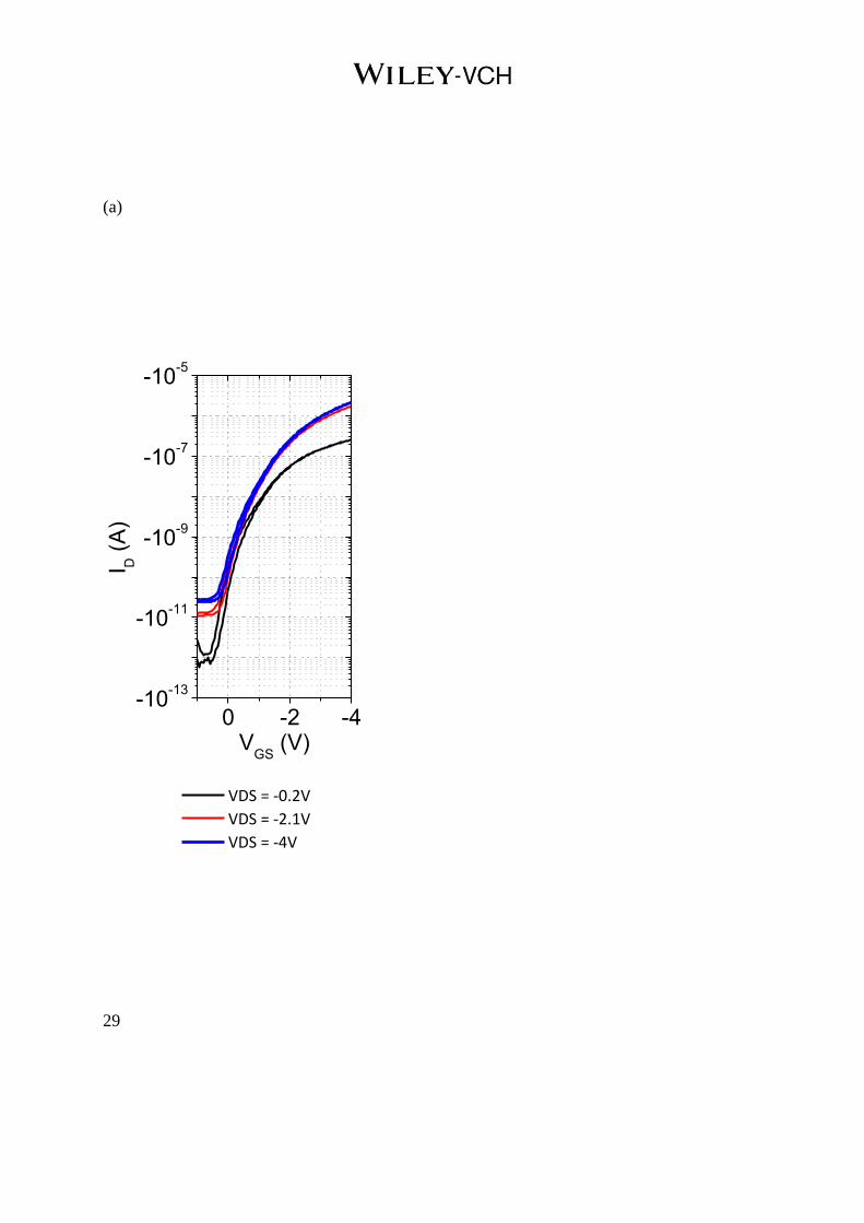
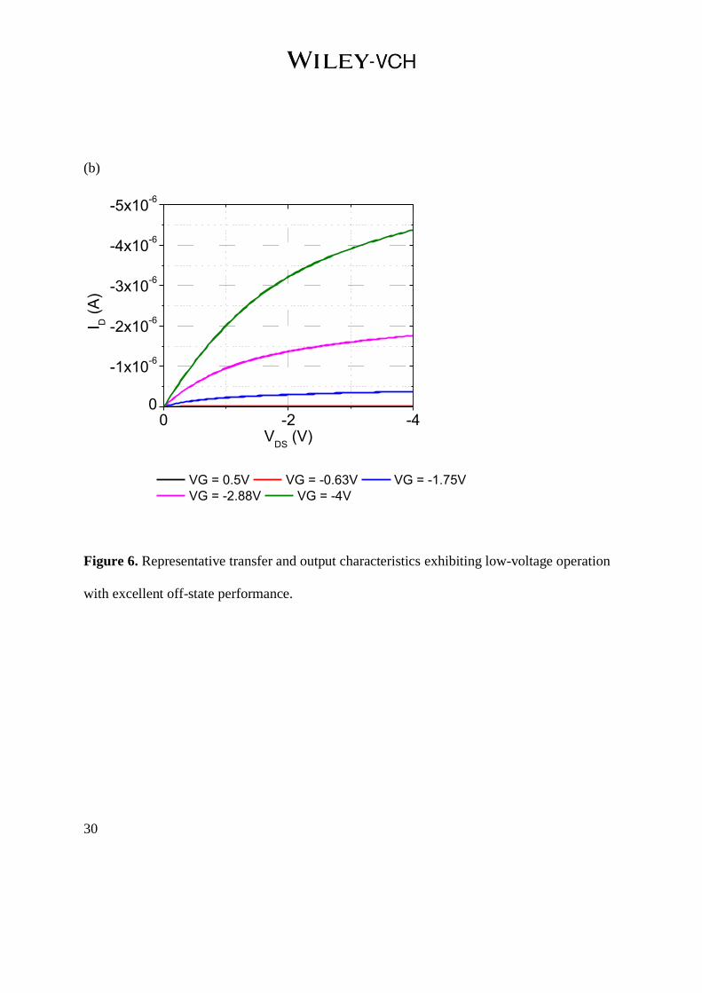
the fabrication of functioning devices with a 120nm thick gravure printed dielectric. Figure 6
shows representative device characteristics for such devices. The operation voltage is below
5V, which is very low for organic transistors, especially when fully printed. On-off ratios
exceeding 105 are achieved at these low voltages. The transition frequency, i.e. the frequency
at which current gain becomes unity, was measured for these low-voltage transistors.
Transistors were tested in an inverter configuration with an external load resistor. A transition
frequency of 96kHz was achieved. To the best of our knowledge this is the highest transition
frequency reported to date for fully high-speed printed transistors on flexible substrates
operating at sub-5V voltages.
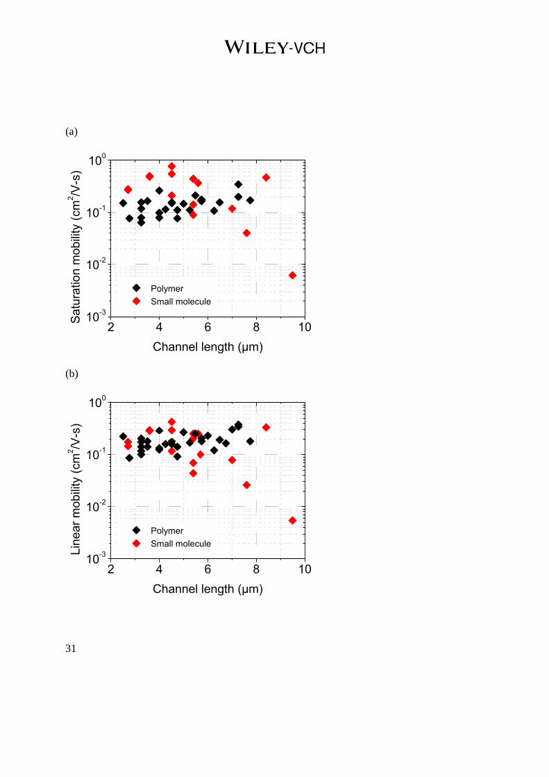
5. Comparison with small molecule semiconductor
One reason for choosing a polymer semiconductor is its better printability compared with
small molecule semiconductors. This facilitates the printing of patterned semiconductor pads.
In addition, the polymer used here is amorphous, which allows for achievement of very good
device-to-device uniformity. In contrast, the performance of small molecule polycrystalline

12
organic semiconductors depends very strongly on the grain size and the location of grain
boundaries. Due to the random nature of the crystallization process, devices with small
molecule semiconductors tend to be more variable than devices with amorphous
semiconductors. Furthermore, polycrystalline semiconductors have larger surface roughness
due to grain boundaries that can be problematic for the yield of the dielectric deposited on top.
Here, we compare our amorphous polymer TFTs with devices fabricated using a state-of-the-
art polycrystalline small molecule semiconductor (Lisicon® S1200) supplied by EMD
Performance Materials Corp. These small molecule devices were fabricated with a very
similar process except the small molecule semiconductor was polycrystalline and not
patterned, the dielectric was 200nm thick and the gate was patterned by inkjet printing.[22]
Figure 7 shows the difference in electrical performance between the polymer and the small
molecule devices. The improved uniformity of the polymer devices both in the on- and the
off-state is clearly visible. Small molecule devices typically exhibit better on-state
performance due to their crystallinity. This can be observed in the saturation mobility. Linear
mobility is similar for the polymer and the small molecule devices because of the excellent
contact resistance achieved here. Off-state performance is improved significantly by using the
polymer semiconductor because of the thinner dielectric and the patterning of the
semiconductor. This allows the polymer devices to be operated at significantly lower voltages.

13
6. Discussion
When designing and fabricating fully-printed devices, it is imperative to consider the device
as a whole, with a particular focus on the layer interactions. For example, AC performance is
boosted by scaling down the width of the source-drain electrodes and the channel length. This
creates a need to scale down the thicknesses of the other layers to maintain good device
electrostatic control. Due to the shorter channel length, contact resistance becomes more
dominant relative to the reduced channel resistance. Since holes are conducted through the
thickness of the semiconductor layer, the semiconductor thickness needs to be scaled down as
the source and drain dimensions are scaled down; this also facilitates improved swing by
improving gate control over the entire channel film. Quantitatively, on-current scales linearly
with the reciprocal of the channel length (1/L) i.e. channel resistance scales linearly with
channel length. Contact resistance due to conduction through the thickness of the
semiconductor film scales linearly with the thickness of the semiconductor film. Thus, as
channel length is scaled down, semiconductor film thickness needs to be scaled down by the
same factor to maintain the same impact of contact resistance due to conduction through the
thickness of the semiconductor. Similarly, shorter channels result in a need for a thinner gate
dielectric. As the source and drain electrodes are brought closer together, the effect of the
drain field on the channel region increases, which will degrade off-state performance and
increase leakage current. To counter this increased drain field, the gate field needs to be
increased accordingly, which can be achieved by scaling down the thickness of the gate
dielectric. If the dielectric thickness is scaled down by the same factor as the channel length,
14
the operating voltage can also be scaled down by this factor. In this case, all the electric fields
have stayed constant and the electrostatic integrity of the device has been maintained during
scaling. These considerations are well known from classical MOSFET scaling. Here, we
apply these principles, for the first time, to fully high-speed printed OTFTs. By printing every
layer with gravure at 1m/s, we demonstrate that scaling of fully high-speed printed devices is
possible, and show that high performance organic transistors can indeed be delivered using
high-speed printing processes. This is a major step towards the manufacturability of printed
OTFTs with high-throughput techniques to fully benefit from the promise of low-cost
fabrication.
7. Conclusions
Fully gravure printed organic thin-film transistors are demonstrated. Every transistor layer is
high-speed printed at 1m/s. Highly-scaled source drain lines are printed with high yield down
to 5µm linewidth and spacing. An amorphous polymer semiconductor is used for its good
printability and uniformity. By patterning the semiconductor and scaling the dielectric, good
off-state performance is achieved allowing operation below 5V. This is a significant step
towards the realization of fully high-speed printed, low-cost, high-performance electronic
systems.

15
8. Experimental
8.1. Materials
Devices were fabricated on planarized polyethylene naphthalate (PEN) substrates (PQA1)
provided by DuPont Teijin Films. The source and drain electrodes were printed using a silver
nanoparticle ink (NPS) purchased from Harima Chemicals Group. The viscosity of this ink
was adjusted to 86cP by dilution with its solvent AF5. The active organic materials were
provided by EMD Performance Materials Corp. (an affiliate of Merck KGaA, Darmstadt,
Germany): lisicon® M001 (surface treatment for the source and drain electrodes, used as
received), lisicon® SP400 (amorphous polymer semiconductor, diluted with mesitylene and
1-methyl naphthalene) and lisicon® D320 (gate dielectric polymer ink, diluted with decane).
The gate electrode was printed using another silver nanoparticle ink (Silverjet DGP 40LT-
15C) as received from Advanced Nano Products (ANP). Three different types of doctor
blades with different tip thicknesses (60µm, 75µm, 95µm) were used for gravure printing as
supplied by Max Daetwyler Corporation.
8.2. Fabrication processes and characterization
Top-gate bottom-contact OTFTs were fabricated. All layers were printed using gravure
printing. All layers were printed at the maximum print speed achievable on our laboratory
scale printer: 1m/s. PEN substrates were laser cut and cleaned by sonication in acetone and
isopropanol. Substrates were treated with a 30 seconds, 50W air plasma before printing of the
source and drain electrodes. The source and drain electrodes were printed using inverse direct
16
gravure. Silicon printing plates were fabricated using conventional microfabrication.[23]
The
cells that make up the pattern are etched into the silicon using KOH to achieve an inverted
pyramid cell shape. The cell width was varied from 3 to 7.5µm whilst the cell gap was kept
constant at 0.1 times the cell width. After printing of the source and drain electrodes, the
silver ink was sintered at 220°C for 2 hours with a slow ramp rate of 3°C/min to improve
electrode adhesion to the substrate. Before printing of the semiconductor, a two-step surface
treatment was applied to improve contact resistance.[21]
First, the source and drain electrodes
were exposed to a mild 10W RF plasma in air for 30 seconds. Then, samples were dried at
100°C for 5 minutes to remove any residual moisture before applying a self-assembled
monolayer (SAM). This drying step is critical to achieve good adhesion of the source and
drain electrodes to the substrate during the subsequent semiconductor printing step. Lisicon®
M001 was applied by drop casting. After drying, the samples were rinsed with isopropyl
alcohol, dried again and dried at 100°C for 1 minute. This surface treatment process could
easily be implemented with a simple roll-to-roll compatible technique such as blade coating
and was thus not implemented with gravure. The semiconductor was gravure printed using
conventional direct gravure with a metal roll fabricated by electromechanical engraving
purchased from RotaDyne. The semiconductor was patterned by using rectangular cell
patterns. The gate dielectric layer was blanket printed using a roll purchased from IGT
Testing Systems (402.101, 45µm cell depth). In order to improve thickness uniformity, the
printed dielectric film was allowed to level in an enclosed environment for 1 hour before
17
drying at 100°C for 5 minutes. Before printing of the gate, the gate dielectric was treated with
a mild air plasma (25W, 10 seconds) to increase the surface energy. The gate electrode was
patterned by using the same electromechanically engraved roll purchased from RotaDyne.
The gate was sintered for 5 minutes at 100°C with a ramp rate of 2°C/minute. Transistor
characteristics were measured using an Agilent 4156C semiconductor parameter analyzer in a
nitrogen atmosphere. All fabrication steps were performed in air. Contact resistance was
extracted using the transmission line method. The transition frequency was measured by
connecting an external resistor to the TFT and applying an AC signal to the gate with an HP
33120A function generator. The output was measured using a Tektronix TDS 3014
oscilloscope.
Supporting Information
Supporting Information is available from the Wiley Online Library or from the author.
Acknowledgements
We acknowledge EMD Performance Materials Corp. (an affiliate of Merck KGaA, Darmstadt,
Germany) for providing the active organic materials, Dupont Teijin Films for providing the
PEN plastic substrates and Max Daetwyler Corporation for providing the doctor blades. This
work is funded in part by EMD Performance Materials Corp.

18
[1] V. Subramanian, J. Cen, A. de la Fuente Vornbrock, G. Grau, H. Kang, R.
Kitsomboonloha, D. Soltman, H.-Y. Tseng, Proc. IEEE 2015, 103, 567.
[2] D. Tobjörk, R. Österbacka, Adv. Mater. 2011, 23, 1935.
[3] G. Grau, R. Kitsomboonloha, S. L. Swisher, H. Kang, V. Subramanian, Adv. Funct.
Mater. 2014, 24, 5067.
[4] Namsoo Lim, Jaeyoung Kim, Soojin Lee, Namyoung Kim, Gyoujin Cho, Adv. Packag.
IEEE Trans. On 2009, 32, 72.
[5] T. Sekitani, H. Nakajima, H. Maeda, T. Fukushima, T. Aida, K. Hata, T. Someya, Nat
Mater 2009, 8, 494.
[6] J. B. Chang, V. Liu, V. Subramanian, K. Sivula, C. Luscombe, A. Murphy, J. Liu, J. M.
J. Frechet, J. Appl. Phys. 2006, 100, 014506.
[7] T. Someya, Y. Kato, T. Sekitani, S. Iba, Y. Noguchi, Y. Murase, H. Kawaguchi, T.
Sakurai, Proc. Natl. Acad. Sci. U. S. A. 2005, 102, 12321.
[8] J. E. Anthony, D. L. Eaton, S. R. Parkin, Org. Lett. 2002, 4, 15.
[9] R. Hamilton, J. Smith, S. Ogier, M. Heeney, J. E. Anthony, I. McCulloch, J. Veres, D. D.
C. Bradley, T. D. Anthopoulos, Adv. Mater. 2009, 21, 1166.
[10] J. Smith, R. Hamilton, I. McCulloch, N. Stingelin-Stutzmann, M. Heeney, D. D. C.
Bradley, T. D. Anthopoulos, J. Mater. Chem. 2010, 20, 2562.
[11] H. Minemawari, T. Yamada, H. Matsui, J. Tsutsumi, S. Haas, R. Chiba, R. Kumai, T.
Hasegawa, Nature 2011, 475, 364.
[12] Y. Yuan, G. Giri, A. L. Ayzner, A. P. Zoombelt, S. C. B. Mannsfeld, J. Chen, D.
Nordlund, M. F. Toney, J. Huang, Z. Bao, Nat. Commun. 2014, 5, DOI
10.1038/ncomms4005.
[13] G. Giri, E. Miller, Z. Bao, J. Mater. Res. 2014, 29, 2615.
[14] G. Grau, R. Kitsomboonloha, H. Kang, V. Subramanian, Org. Electron. 2015, 20, 150.
[15] M.-H. Yoon, H. Yan, A. Facchetti, T. J. Marks, J. Am. Chem. Soc. 2005, 127, 10388.
[16] Y. D. Park, D. H. Kim, Y. Jang, M. Hwang, J. A. Lim, K. Cho, Appl. Phys. Lett. 2005,
87, 243509.
[17] S. Lai, P. Cosseddu, G. C. Gazzadi, M. Barbaro, A. Bonfiglio, Org. Electron. 2013, 14,
754.
[18] K. Fukuda, Y. Takeda, M. Mizukami, D. Kumaki, S. Tokito, Sci. Rep. 2014, 4, DOI
10.1038/srep03947.
[19] A. Pierre, M. Sadeghi, M. M. Payne, A. Facchetti, J. E. Anthony, A. C. Arias, Adv.
Mater. 2014, 26, 5722.
[20] K. Fukuda, Y. Yoshimura, T. Okamoto, Y. Takeda, D. Kumaki, Y. Katayama, S. Tokito,
Adv. Electron. Mater. 2015, 1, n/a.
[21] H. Kang, R. Kitsomboonloha, K. Ulmer, L. Stecker, G. Grau, J. Jang, V. Subramanian,
Org. Electron. 2014, 15, 3639.
[22] R. Kitsomboonloha, H. Kang, G. Grau, W. J. Scheideler, V. Subramanian, Adv. Electron.
Mater. 2015, DOI 10.1002/aelm.201500155.

19
[23] R. Kitsomboonloha, S. J. S. Morris, X. Rong, V. Subramanian, Langmuir 2012, 28,
16711.
[24] G. Grau, R. Kitsomboonloha, V. Subramanian, in Proc SPIE 9568, San Diego, 2015, p.
95680M.
[25] G. Grau, W. J. Scheideler, V. Subramanian, in Proc SPIE 9569, San Diego, 2015, p.
95690B–1.
[26] R. Kitsomboonloha, V. Subramanian, Langmuir 2014, 30, 3612.
[27] G. Hernandez-Sosa, N. Bornemann, I. Ringle, M. Agari, E. Dörsam, N. Mechau, U.
Lemmer, Adv. Funct. Mater. 2013, 23, 3164.

20
(a)
(b)
(i) (ii)
(iii) (iv)

21
Figure 1. (a) Overview of the gravure printing process. Patterns are defined by recessed cells
that are engraved into a roll. The cells are filled with ink from an ink reservoir. Excess ink is
wiped off the roll surface using a doctor blade. Ink is transferred from the roll to a substrate
such as plastic or paper. Ink spreads on the substrate to fill in the gaps between individual
cells. (b) Overview of fabrication process and device structure. (i) Highly-scaled silver
electrodes are gravure printed on cleaned PEN plastic substrates. (ii) After a self-assembled
monolayer treatment, the polymer semiconductor is patterned using gravure printing. (iii) The
dielectric is blanket printed using gravure. (iv) The silver gate electrode is patterned by
gravure printing. All printing steps are performed at 1m/s in air.

22
(a) (b)
0 5 10 150%
25%
50%
75%
100%
Yie
ld
Printed channel length (µm)
Start Middle End0%
25%
50%
75%
100%
Blade tip thickness
60m
75m
95mY
ield
Position in print
(c)
Figure 2. Printing yield of source-drain patterns. (a) Yield is close to 100% for channel
lengths above 5µm. Below 5µm, the number of merged lines increases significantly. (b) Yield
depends significantly on the thickness of the doctor blade tip. 60µm blades show significant
degradation during prints due to wear. 95µm blades show decreased yield due to insufficient
pressure. 75µm blades exhibit good yield with reduced wear. (c) Cross-sectional micrographs
showing the tip of the doctor blade for three different blade tip thicknesses, which is measured
at the very tip of the blade.

23
(a)
9cP:
24cP:
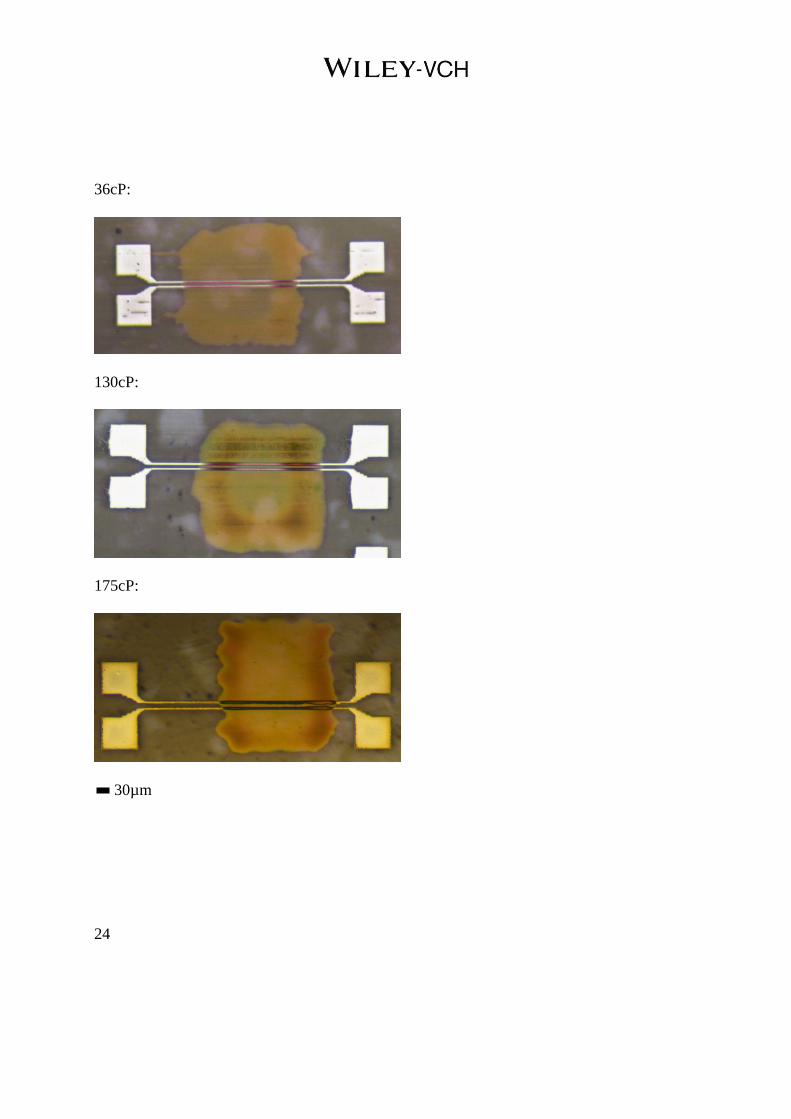
24
36cP:
130cP:
175cP:
30µm

25
(b)
0 200 400 600 8000
50
100
150
200 24cP
36cP
130cP
175cP
He
ight (n
m)
Position (µm)
Figure 3. Semiconductor pattern definition for different ink viscosities. (a) Optical
micrographs showing printed semiconductor patterns on top of printed source and drain lines.
Lateral pattern definition improves with increased viscosity. 9cP spreads uncontrollably. 24cP
and above exhibits defined patterns. (b) Pattern thickness increases and relative coffee ring
height decreases with increasing viscosity.

26
(a)
(b)
10 1000
1x10⁸
2x10⁸
3x10⁸
Co
nta
ct re
sis
tance
(µ
m)
Viscosity (cP)
27
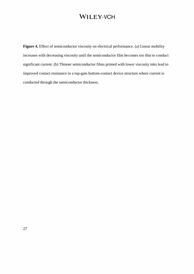
Figure 4. Effect of semiconductor viscosity on electrical performance. (a) Linear mobility
increases with decreasing viscosity until the semiconductor film becomes too thin to conduct
significant current. (b) Thinner semiconductor films printed with lower viscosity inks lead to
improved contact resistance in a top-gate bottom-contact device structure where current is
conducted through the semiconductor thickness.

28
(a)
(b)
Figure 5. Off-state performance improves significantly with thinner gate dielectrics due to
better gate control.
29
(a)
0 -2 -4-10
-13
-10-11
-10-9
-10-7
-10-5
VDS = -0.2V
VDS = -2.1V
VDS = -4V
I D (
A)
VGS
(V)
30
(b)
0 -2 -40
-1x10⁻⁶
-2x10⁻⁶
-3x10⁻⁶
-4x10⁻⁶
-5x10⁻⁶
I D (
A)
VDS
(V)
VG = 0.5V VG = -0.63V VG = -1.75V
VG = -2.88V VG = -4V
Figure 6. Representative transfer and output characteristics exhibiting low-voltage operation
with excellent off-state performance.
31
(a)
2 4 6 8 1010
-3
10-2
10-1
100
Satu
ratio
n m
obili
ty (
cm
2/V
-s)
Polymer
Small molecule
Channel length (µm)
(b)
2 4 6 8 1010
-3
10-2
10-1
100
Lin
ear
mo
bili
ty (
cm
2/V
-s)
Polymer
Small molecule
Channel length (µm)

32
(c)
2 4 6 8 100
5
10
15
Sw
ing (
V/d
ec)
Polymer
Small molecule
Channel length (µm)
(d)
2 4 6 8 10-2
0
2
4
6
Thre
shold
voltage (
V)
Polymer
Small molecule
Channel length (µm)

33
Figure 7. Comparison of amorphous polymer and polycrystalline small molecule
semiconductor devices. Polymer devices exhibit better uniformity. (a) Small molecule devices
exhibit slightly higher saturation mobility. (b) Linear mobility is comparable due to the
excellent contact resistance achieved here. (c) and (d) Both swing and threshold voltage are
significantly better for the polymer devices due to a thinner gate dielectric and patterning of
the semiconductor.

34
The table of contents entry
Fully high-speed printed OTFTs are demonstrated. All layers are gravure printed at 1m/s
with source-drain and channel dimensions of 5µm. Good uniformity is achieved by
employing an amorphous polymer semiconductor. By patterning the semiconductor and
scaling the dielectric, low-voltage operation below 5V is achieved. This is a promising result
for the realization of low-cost, large area, flexible printed systems.
Keyword: Organic thin film transistors (OTFT), gravure printing, printed electronics, high-
speed printing, low variability
Gerd Grau and Vivek Subramanian*

35
Table of Contents Figure

36
Copyright WILEY-VCH Verlag GmbH & Co. KGaA, 69469 Weinheim, Germany, 2013.
Supporting Information
Fully High-Speed Gravure Printed, Low-Variability, High-Performance Organic
Polymer Transistors with Sub-5V Operation
Gerd Grau and Vivek Subramanian*
0 5 100
5
10
Lin
e w
idth
pri
nte
d (
µm
)
Line width plate (µm)
Figure S1. Printed linewidth is linearly related to line width (=cell width) on the printing
plate. Printed line width is slightly enlarged by ink spreading on the substrate.

37
0 5 10 15 200
5
10
15
Ch
an
ne
l le
ng
th p
rin
ted
(µ
m)
Channel length plate (µm)
Figure S2. Printed channel length is linearly related to channel length on the printing plate.
Channel length is reduced by ink spreading on the substrate.

38
0 1 20%
10%
20%
0%
20%
40%
60%
80%
100%
Thickness standard deviation
Dielectric yield
Thic
kness s
tandard
devia
tion
Leveling time (h)
Die
lectr
ic y
ield
Figure S3. Dielectric thickness uniformity and yield are improved significantly by allowing
the film to level in a solvent atmosphere before drying, to remove any non-uniformities after
gravure printing. Data for 300nm thick film.

39
0 100 200 300 400 5000%
25%
50%
75%
100%
Die
lectr
ic y
ield
Dielectric thickness (nm)
Figure S4. The dielectric yield of gravure printed dielectric is perfect down to a thickness of
300nm. Below this thickness, further improvements in yield are required.

40
0 5 10 15 200
50
100
150
He
ight (n
m)
Position (µm)
Figure S 5. Height profile of source and drain lines. The average RMS surface roughness is
15.3nm. Improvements in source and drain surface roughness might improve dielectric yield.