
Getting Started with 'Proteus 8' - Sanad AlTaher
12
0 Jordan University of Science and technology Electrical Engineering Department EE346 – Microcontrollers Lab Getting Started with ‘Proteus 8’ Prepared by: Mohammad-Sanad AlTaher Supervised by: Prof. Ahmad Abu-El-Heija
-
Upload
khangminh22 -
Category
Documents
-
view
4 -
download
0
Transcript of Getting Started with 'Proteus 8' - Sanad AlTaher

0
Jordan University of Science and technology
Electrical Engineering Department
EE346 – Microcontrollers Lab
Getting Started with ‘Proteus 8’
Prepared by: Mohammad-Sanad AlTaher Supervised by: Prof. Ahmad Abu-El-Heija
1
Introduction & Outcomes:
In this guide, the basics of Schematic Capture in Proteus Design Suite will be covered step-by-step. After reading, the
student should be familiar with the Proteus interface and be capable of constructing different digital circuits.
This document is not a thorough guide to Proteus, it is meant to cover Proteus use cases for EE346 – Microcontrollers
Lab only and will not cover PCB layout, Visual Design, and other modules of the software as they are not needed in
the Microcontrollers course. Proteus is a powerful tool that all EE students should explore.
Proteus 8.9 Professional SP0 will be used to demonstrate the steps; however, steps should also apply to other versions
of Proteus 8.
Contents:
1. Creating a file
2. Interface
3. Collecting Parts
4. Connecting a Circuit
5. Running the Simulator
6. Saving and Exporting
1. Creating a File:
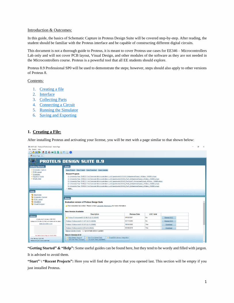
After installing Proteus and activating your license, you will be met with a page similar to that shown below:
“Getting Started” & “Help”: Some useful guides can be found here, but they tend to be wordy and filled with jargon.
It is advised to avoid them.
“Start” \ “Recent Projects”: Here you will find the projects that you opened last. This section will be empty if you
just installed Proteus.
2
“News”: This section will contain news about your current license, recent versions of the software, and links to basic
video tutorials that you might find helpful.
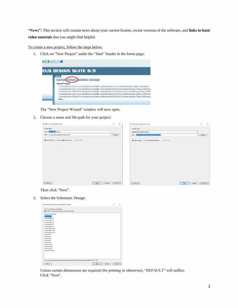
To create a new project, follow the steps below:
1. Click on “New Project” under the “Start” header in the home page:
The “New Project Wizard” window will now open.
2. Choose a name and file-path for your project:
Then click “Next”.
3. Select the Schematic Design:
Unless certain dimensions are required (for printing or otherwise), “DEFAULT” will suffice.
Click “Next”.
3
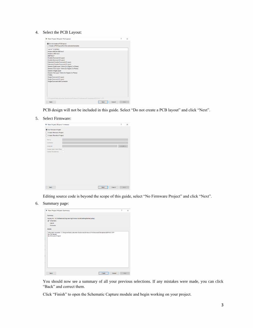
4. Select the PCB Layout:
PCB design will not be included in this guide. Select “Do not create a PCB layout” and click “Next”.
5. Select Firmware:
Editing source code is beyond the scope of this guide, select “No Firmware Project” and click “Next”.
6. Summary page:
You should now see a summary of all your previous selections. If any mistakes were made, you can click
“Back” and correct them.
Click “Finish” to open the Schematic Capture module and begin working on your project.
4
Alternatively: Creating a new project can be done by clicking “Ctrl” + “N” or from the “File” menu in the menu bar,
then follow steps 2 through 6.
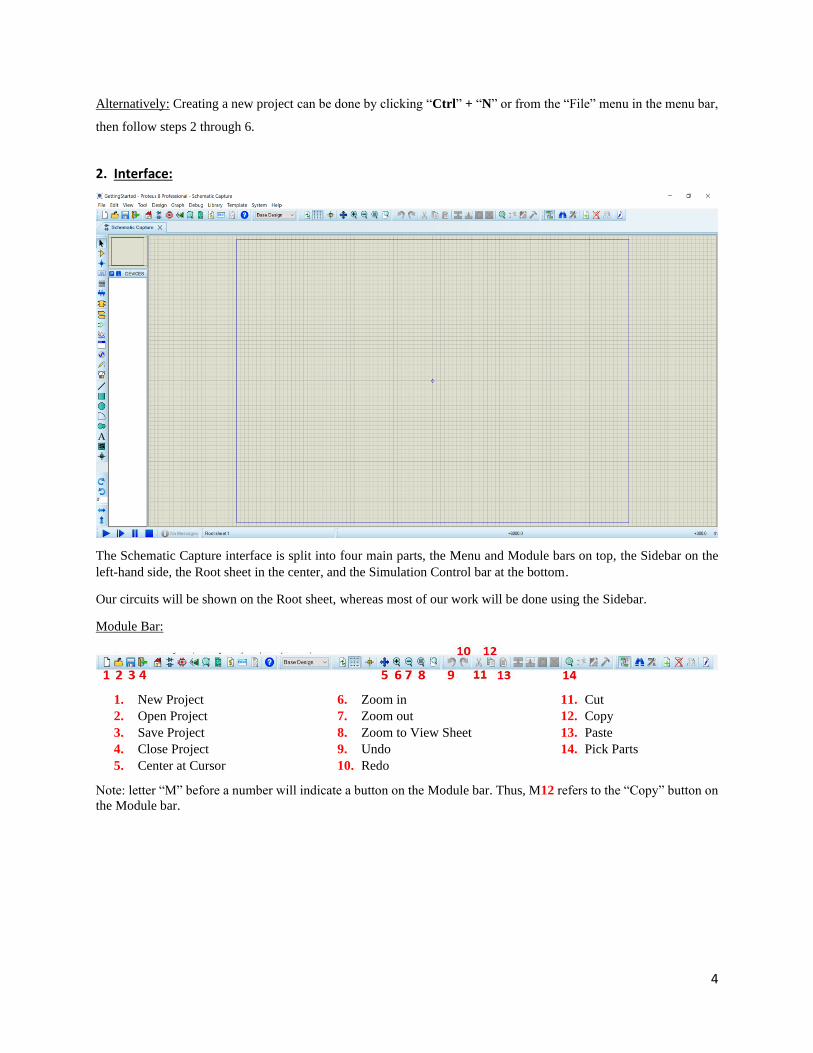
2. Interface:
The Schematic Capture interface is split into four main parts, the Menu and Module bars on top, the Sidebar on the
left-hand side, the Root sheet in the center, and the Simulation Control bar at the bottom.
Our circuits will be shown on the Root sheet, whereas most of our work will be done using the Sidebar.
Module Bar:
1. New Project
2. Open Project
3. Save Project
4. Close Project
5. Center at Cursor
6. Zoom in
7. Zoom out
8. Zoom to View Sheet
9. Undo
10. Redo
11. Cut
12. Copy
13. Paste
14. Pick Parts
Note: letter “M” before a number will indicate a button on the Module bar. Thus, M12 refers to the “Copy” button on
the Module bar.
5
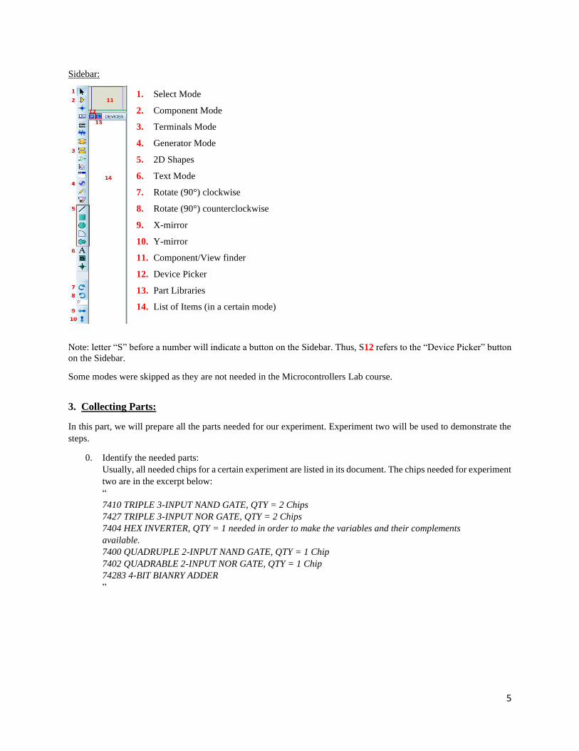
Sidebar:
1. Select Mode
2. Component Mode
3. Terminals Mode
4. Generator Mode
5. 2D Shapes
6. Text Mode
7. Rotate (90°) clockwise
8. Rotate (90°) counterclockwise
9. X-mirror
10. Y-mirror
11. Component/View finder
12. Device Picker
13. Part Libraries
14. List of Items (in a certain mode)
Note: letter “S” before a number will indicate a button on the Sidebar. Thus, S12 refers to the “Device Picker” button
on the Sidebar.
Some modes were skipped as they are not needed in the Microcontrollers Lab course.
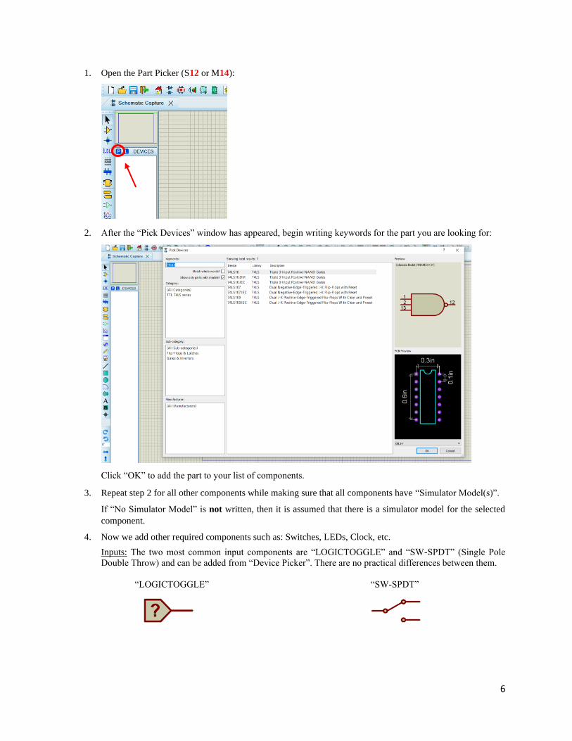
3. Collecting Parts:
In this part, we will prepare all the parts needed for our experiment. Experiment two will be used to demonstrate the
steps.
0. Identify the needed parts:
Usually, all needed chips for a certain experiment are listed in its document. The chips needed for experiment
two are in the excerpt below:
“
7410 TRIPLE 3-INPUT NAND GATE, QTY = 2 Chips
7427 TRIPLE 3-INPUT NOR GATE, QTY = 2 Chips
7404 HEX INVERTER, QTY = 1 needed in order to make the variables and their complements
available.
7400 QUADRUPLE 2-INPUT NAND GATE, QTY = 1 Chip
7402 QUADRABLE 2-INPUT NOR GATE, QTY = 1 Chip
74283 4-BIT BIANRY ADDER
”
6
1. Open the Part Picker (S12 or M14):
2. After the “Pick Devices” window has appeared, begin writing keywords for the part you are looking for:
Click “OK” to add the part to your list of components.
3. Repeat step 2 for all other components while making sure that all components have “Simulator Model(s)”.
If “No Simulator Model” is not written, then it is assumed that there is a simulator model for the selected
component.
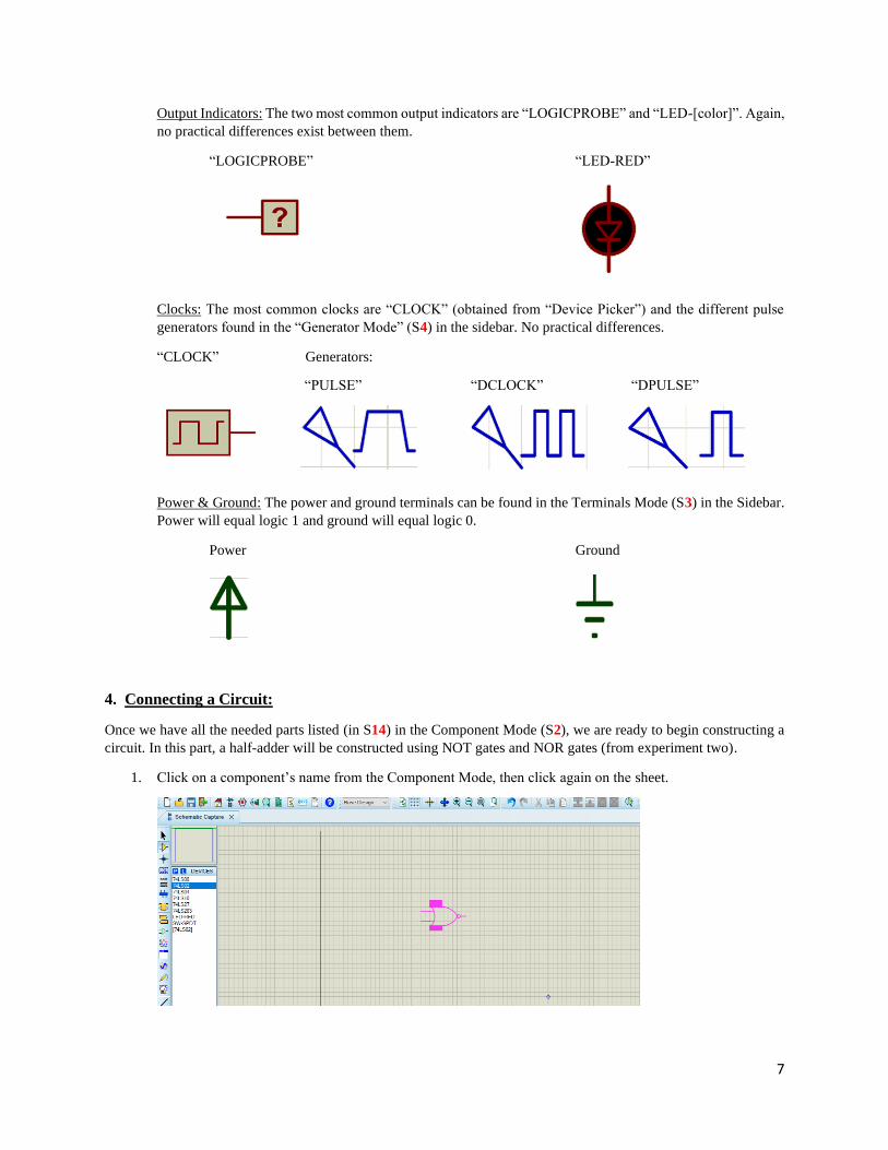
4. Now we add other required components such as: Switches, LEDs, Clock, etc.
Inputs: The two most common input components are “LOGICTOGGLE” and “SW-SPDT” (Single Pole
Double Throw) and can be added from “Device Picker”. There are no practical differences between them.
“LOGICTOGGLE” “SW-SPDT”
7
Output Indicators: The two most common output indicators are “LOGICPROBE” and “LED-[color]”. Again,
no practical differences exist between them.
“LOGICPROBE” “LED-RED”
Clocks: The most common clocks are “CLOCK” (obtained from “Device Picker”) and the different pulse
generators found in the “Generator Mode” (S4) in the sidebar. No practical differences.
“CLOCK” Generators:
“PULSE” “DCLOCK” “DPULSE”
Power & Ground: The power and ground terminals can be found in the Terminals Mode (S3) in the Sidebar.
Power will equal logic 1 and ground will equal logic 0.
Power Ground
4. Connecting a Circuit:
Once we have all the needed parts listed (in S14) in the Component Mode (S2), we are ready to begin constructing a
circuit. In this part, a half-adder will be constructed using NOT gates and NOR gates (from experiment two).
1. Click on a component’s name from the Component Mode, then click again on the sheet.
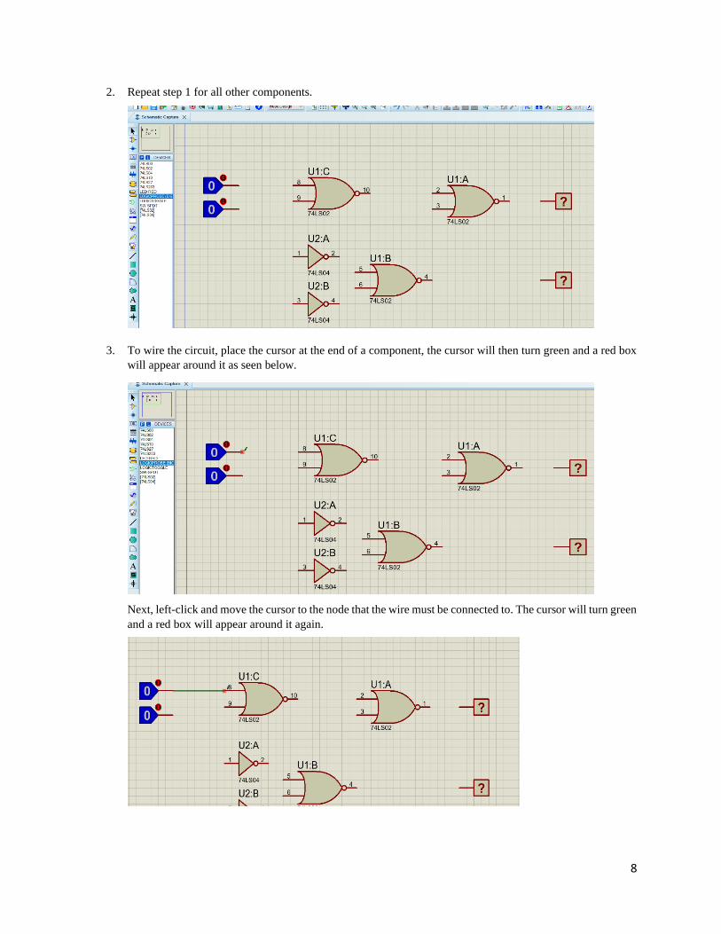
8
2. Repeat step 1 for all other components.
3. To wire the circuit, place the cursor at the end of a component, the cursor will then turn green and a red box
will appear around it as seen below.
Next, left-click and move the cursor to the node that the wire must be connected to. The cursor will turn green
and a red box will appear around it again.
9
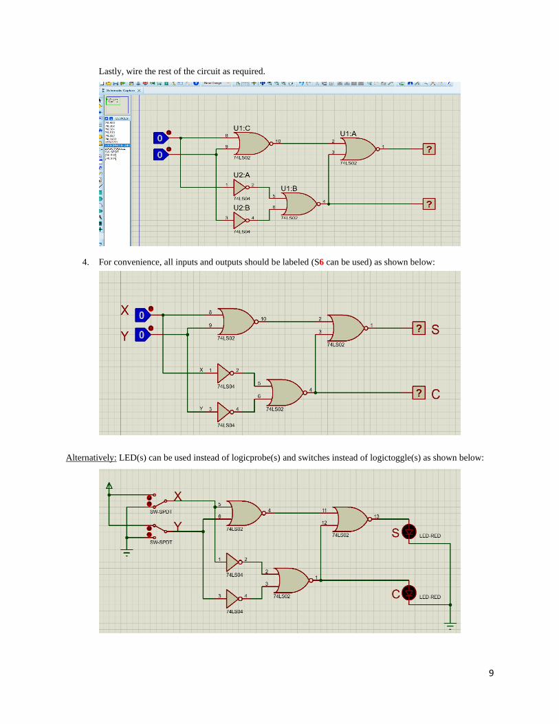
Lastly, wire the rest of the circuit as required.
4. For convenience, all inputs and outputs should be labeled (S6 can be used) as shown below:
Alternatively: LED(s) can be used instead of logicprobe(s) and switches instead of logictoggle(s) as shown below:
10
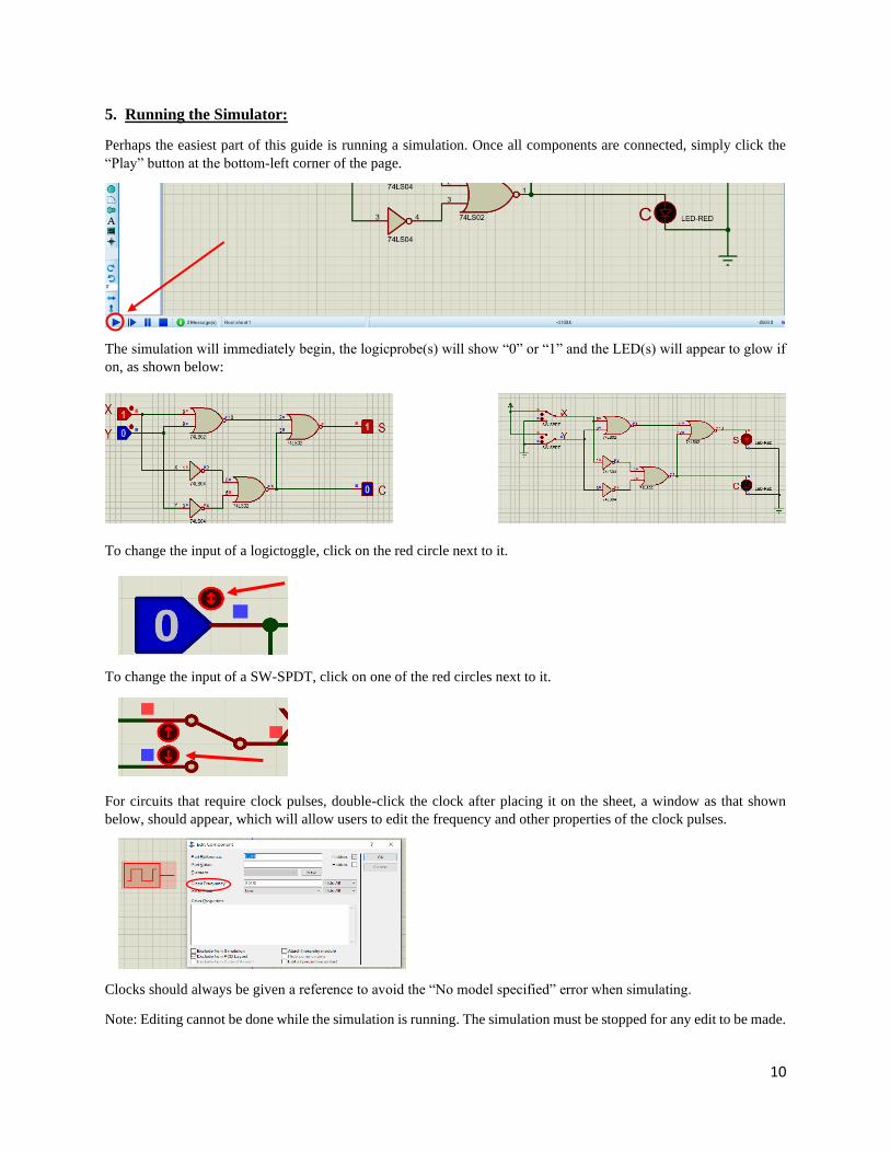
5. Running the Simulator:
Perhaps the easiest part of this guide is running a simulation. Once all components are connected, simply click the
“Play” button at the bottom-left corner of the page.
The simulation will immediately begin, the logicprobe(s) will show “0” or “1” and the LED(s) will appear to glow if
on, as shown below:
To change the input of a logictoggle, click on the red circle next to it.
To change the input of a SW-SPDT, click on one of the red circles next to it.
For circuits that require clock pulses, double-click the clock after placing it on the sheet, a window as that shown
below, should appear, which will allow users to edit the frequency and other properties of the clock pulses.
Clocks should always be given a reference to avoid the “No model specified” error when simulating.
Note: Editing cannot be done while the simulation is running. The simulation must be stopped for any edit to be made.
11
6. Saving and Exporting:
A project can be saved by simply clicking on the save icon (M3) in the Module bar.
Proteus also allows users to export their projects to different formats such as PDF. This can be done from the “Export
Graphics” submenu in the “File” menu.
Miscellaneous Hints & Notes:
• If the “Proteus Demonstration version” is being used, a prompt saying “Saving is disabled in demonstration
version” will appear if the user tries to save. Hence, the demonstration version should be avoided.
• Clocks should always be named to avoid an error.
• Edits cannot be made while the simulation is running. It must be stopped completely.
• It is advised to use LS (Low-power Schottky) or HC (High-speed CMOS) parts, as other parts are simulated
as if ideal, which can introduce errors and the outputs will be indeterminate while simulating.
• Click the scroll wheel (on your mouse) to drag the plane, click again to stop dragging.
• The function keys (on your keyboard) can be used to complete some Module bar operations:
“F5”: Centers the sheet at your cursor (M5).
“F6”: Zoom in (M6).
“F7”: Zoom out (M7).
“F8”: Zoom to view entire sheet, and centers at origin (M8).
“F12”: Start simulation.
• Other useful shortcuts:
“-” and “+” on the number pad can be used to rotate clockwise (S7) and counterclockwise (S8) respectively.
“Ctrl” + “Z”: Undo (M9).
“Ctrl” + “Y”: Redo (M10)
“Ctrl” + “M”: X-mirror (S9).
“Ctrl” + “S”: Save (M3).
“P”: Pick Parts (S12).
• All shortcuts can be seen in the “Set Keyboard Mapping” window that is opened from the “System” menu in
the Menu bar. Shortcuts can also be mapped to keys of your choosing.
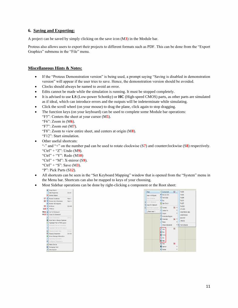
• Most Sidebar operations can be done by right-clicking a component or the Root sheet:


![PIPEPHASE Getting Started Guide[1] - baixardoc](https://static.fdokumen.com/doc/165x107/6315b7d1aca2b42b580df6a1/pipephase-getting-started-guide1-baixardoc.jpg)