Geometrical structure and interface dependence of bias stress induced threshold voltage shift in...
6
Geometrical Structure and Interface Dependence of Bias Stress Induced Threshold Voltage Shift in C 60 -Based OFETs Rizwan Ahmed,* ,†,‡ Andrey Kadashchuk, §,∥ Clemens Simbrunner, † Gü nther Schwabegger, † Muhammad Aslam Baig, ‡ and Helmut Sitter † † Institute of Semiconductor and Solid State Physics, Johannes Kepler University, A-4040 Linz, Austria ‡ National Center for Physics, Quaid-e-Azam University Campus, Islamabad, Pakistan § Institute of Physics, National Academy of Sciences of Ukraine, 03028 Kyiv, Ukraine ∥ IMEC, Kapeldreef 75, B-3001 Leuven, Belgium ABSTRACT: The influence of the nature of interface between organic semiconductor and gate dielectric on bias stress electrical stability of n-type C 60 -based organic field effect transistors (OFETs) was studied. The bias stress induced threshold voltage (V th ) shift was found to depend critically on the OFET device structure: the direction of V th shift in top-gate OFETs was opposite to that in bottom-gate OFETs, while the use of the dual-gate OFET structure resulted in just very small variations in V th . The opposite direction of V th shift is attributed to the different nature of interfaces between C 60 semiconductor and Parylene dielectric in these devices. The V th shift to more positive voltages upon bias stress in bottom-gate C 60 -OFET was similar to that observed for other n-type semiconductors and rationalized by electron trapping in the dielectric or at the gate dielectric/C 60 interface. The opposite direction of V th shift in top-gate C 60 - OFETs is attributed to free radical species created in the course of Parylene deposition on the surface of C 60 during device fabrication, which produce plenty of hole traps. It was also realized that the dual-gate OFETs gives stable characteristics, which are immune to bias stress effects. KEYWORDS: C 60 /Parylene interface, bias stress, n-type OFETs electrical stability, threshold voltage shift, charge trapping, top-gate, bottom-gate and dual-gate OFETs 1. INTRODUCTION In the last two decades, tremendous progress has been made in the development of organic field effect transistors (OFETs). The performance of OFETs has been improved, and now they are comparable to the amorphous silicon transistors. 1−3 The applications are foreseen as a driver of flat panel display, 4 memory devices, 5 smart labels, 6 and biological sensor. 7,8 The stability of OFETs is a critical requirement for practical applications, but the OFETs are giving unstable characteristics under continuous bias stress. 9 The main bias stress induced instability appears as a shift in the threshold voltage (V th ) or as a decrease in drain source current (I DS ) at fixed voltage. 10 Several efforts were made to measure the bias stress induced instabilities in p-type OFETs, 11 but n-type OFETs are still awaiting more attention. 12 The major reasons of bias stress instabilities are the charge trapping in the organic semi- conductor, 13−16 in the gate dielectric, 17,18 or at the interface between active layer and dielectric. 19,20 The nature of interface between the organic semiconductor and the gate dielectric plays a major role in the charge carrier transport of OFETs. 21 In pentacene-based OFETs with an embedded thin layer of copper oxide (CuO), it was found that the trapped electrons at the interface between pentacene and CuO are not easily released, which results in a stable threshold voltage up to 3000 s against the bias stress. 22 The threshold voltage stability of OFETs can be related to the energetic distribution of the barrier heights for charge trapping between organic semiconductor and gate dielectric. The relation of bias stress induced V th shift and trapping energy distribution was analyzed by measuring the temperature dependence of source- drain current decay under gate bias stress. It was noticed that the barrier heights for charge trapping become higher and narrower by using a self-assembled monolayer, resulting in stable transfer characteristics against bias stress without any significant change in V th . 23 The role of a self-assembled monolayer in stabilization of output characteristics was investigated by using di fferent types of self-assembled monolayers in SiO 2 insulator-based pentacene OFETs. The results reveal that bias stress induced V th shift was considerably increased by introducing long chain chemical species on the surface of the insulator, while OFETs with short chain self- assembled monolayers on the surface of SiO 2 give character- istics with stable threshold voltage against continuous gate bias stress. 24 Most of the studies related to interface and V th instabilities are done by using bottom-gate top-contact OFETs, while little attention was given to measure the V th Received: May 27, 2014 Accepted: August 21, 2014 Published: August 21, 2014 Research Article www.acsami.org © 2014 American Chemical Society 15148 dx.doi.org/10.1021/am5032192 | ACS Appl. Mater. Interfaces 2014, 6, 15148−15153 Terms of Use CC-BY
-
Upload
independent -
Category
Documents
-
view
2 -
download
0
Transcript of Geometrical structure and interface dependence of bias stress induced threshold voltage shift in...
Geometrical Structure and Interface Dependence of Bias StressInduced Threshold Voltage Shift in C60-Based OFETsRizwan Ahmed,*,†,‡ Andrey Kadashchuk,§,∥ Clemens Simbrunner,† Gunther Schwabegger,†
Muhammad Aslam Baig,‡ and Helmut Sitter†
†Institute of Semiconductor and Solid State Physics, Johannes Kepler University, A-4040 Linz, Austria‡National Center for Physics, Quaid-e-Azam University Campus, Islamabad, Pakistan§Institute of Physics, National Academy of Sciences of Ukraine, 03028 Kyiv, Ukraine∥IMEC, Kapeldreef 75, B-3001 Leuven, Belgium
ABSTRACT: The influence of the nature of interface between organic semiconductorand gate dielectric on bias stress electrical stability of n-type C60-based organic fieldeffect transistors (OFETs) was studied. The bias stress induced threshold voltage (Vth)shift was found to depend critically on the OFET device structure: the direction of Vthshift in top-gate OFETs was opposite to that in bottom-gate OFETs, while the use ofthe dual-gate OFET structure resulted in just very small variations in Vth. The oppositedirection of Vth shift is attributed to the different nature of interfaces between C60semiconductor and Parylene dielectric in these devices. The Vth shift to more positivevoltages upon bias stress in bottom-gate C60-OFET was similar to that observed forother n-type semiconductors and rationalized by electron trapping in the dielectric orat the gate dielectric/C60 interface. The opposite direction of Vth shift in top-gate C60-OFETs is attributed to free radical species created in the course of Parylene depositionon the surface of C60 during device fabrication, which produce plenty of hole traps. Itwas also realized that the dual-gate OFETs gives stable characteristics, which are immune to bias stress effects.
KEYWORDS: C60/Parylene interface, bias stress, n-type OFETs electrical stability, threshold voltage shift, charge trapping, top-gate,bottom-gate and dual-gate OFETs
1. INTRODUCTION
In the last two decades, tremendous progress has been made inthe development of organic field effect transistors (OFETs).The performance of OFETs has been improved, and now theyare comparable to the amorphous silicon transistors.1−3 Theapplications are foreseen as a driver of flat panel display,4
memory devices,5 smart labels,6 and biological sensor.7,8 Thestability of OFETs is a critical requirement for practicalapplications, but the OFETs are giving unstable characteristicsunder continuous bias stress.9 The main bias stress inducedinstability appears as a shift in the threshold voltage (Vth) or asa decrease in drain source current (IDS) at fixed voltage.10
Several efforts were made to measure the bias stress inducedinstabilities in p-type OFETs,11 but n-type OFETs are stillawaiting more attention.12 The major reasons of bias stressinstabilities are the charge trapping in the organic semi-conductor,13−16 in the gate dielectric,17,18 or at the interfacebetween active layer and dielectric.19,20
The nature of interface between the organic semiconductorand the gate dielectric plays a major role in the charge carriertransport of OFETs.21 In pentacene-based OFETs with anembedded thin layer of copper oxide (CuO), it was found thatthe trapped electrons at the interface between pentacene andCuO are not easily released, which results in a stable thresholdvoltage up to 3000 s against the bias stress.22 The threshold
voltage stability of OFETs can be related to the energeticdistribution of the barrier heights for charge trapping betweenorganic semiconductor and gate dielectric. The relation of biasstress induced Vth shift and trapping energy distribution wasanalyzed by measuring the temperature dependence of source-drain current decay under gate bias stress. It was noticed thatthe barrier heights for charge trapping become higher andnarrower by using a self-assembled monolayer, resulting instable transfer characteristics against bias stress without anysignificant change in Vth.
23 The role of a self-assembledmonolayer in stabilization of output characteristics wasinvestigated by using different types of self-assembledmonolayers in SiO2 insulator-based pentacene OFETs. Theresults reveal that bias stress induced Vth shift was considerablyincreased by introducing long chain chemical species on thesurface of the insulator, while OFETs with short chain self-assembled monolayers on the surface of SiO2 give character-istics with stable threshold voltage against continuous gate biasstress.24 Most of the studies related to interface and Vth
instabilities are done by using bottom-gate top-contactOFETs, while little attention was given to measure the Vth
Received: May 27, 2014Accepted: August 21, 2014Published: August 21, 2014
Research Article
www.acsami.org
© 2014 American Chemical Society 15148 dx.doi.org/10.1021/am5032192 | ACS Appl. Mater. Interfaces 2014, 6, 15148−15153
Terms of Use CC-BY
stability of top-gate OFETs.25,26 It has been already found thatthe deposition technique and the order of deposition of organicsemiconductors and gate insulator have a huge influence on theformation of the active interface,27 and the nature of interfacehas a direct impact on charge carrier transport in OFETs.To investigate the role of the interface on bias stress induced
threshold voltage instabilities, the C60-based top-gate andbottom-gate OFETs with Parylene as a gate dielectric werestudied. It was observed that the direction of bias stress inducedVth shift in top-gate OFETs was opposite to the bottom gateOFETs. The investigations were further extended, andexperimental results reveal that the use of dual-gate can resultin stable characteristics with small variations in Vth with gatebias stress.
2. EXPERIMENTAL DETAILSFor the fabrication of different device geometry OFETs, a 0.5 mmwide and 100 nm thick gate electrode of Aluminum was evaporated onglass substrate by using shadow mask with a background pressure of10−6 mbar. Parylene was used as dielectric and the deposition wasdone in a homemade system which has three temperature zones. First,the dimer dichloro-di-p-xylylene is evaporated at a temperature of 100°C, next the vapor is passing a high temperature zone (750 °C) wherepyrolysis leads to cleavage of the dimers. The resulting monomers arefinally deposited at room temperature on the sample surface, wherethey spontaneously polymerize to form a transparent and conformalthin film. The process is carried out at a pressure of 10−2 mbar, and forthe bottom-gate OFET fabrication a dielectric layer thickness of 1 μmwas used. C60 was used as received from MER Corp. The 150 nm thickorganic semiconductor film of C60 was grown by hot-wall epitaxy(HWE) at a substrate temperature Tsub = 100 °C, source temperatureTs = 360 °C, and wall temperature Twall = 400 °C with a backgroundpressure of 10−6 mbar. For top contact electrodes, 70 nm thick Al wasevaporated under high vacuum of 10−6 mbar, using a shadow mask.The channel length L and width W in the OFETs were 70 μm and 1.5mm, respectively. In a similar way (except the order of deposition ofC60/Parylene), the top-gate bottom-contacts and dual-gate OFETswere also fabricated. A dual-gate transistor in fact consists of a bottom-gate top-contacts transistor with an additional second gate and seconddielectric layer. Device transportation from the fabrication laboratoryto measurement laboratory was carried out in a nitrogen-filled box.All OFETs were characterized at room temperature under N2
atmosphere inside a glovebox, to avoid exposure to ambient humidityand oxygen (both values were maintained below 0.5 ppm). More detailof experimental procedure can be found elsewhere.28,29 For applyingthe gate voltage (VGS) and measuring the leakage current a Keithley6487 Pico-Ampere meter with included voltage source was used,whereas the source-drain voltage (VSD) characteristics were recordedby a Keithley 2400 voltage source unit.The electrical stress was applied to each type device in matrix form.
During the bias stress time, the gate voltage was continuously variedfrom −10 to 50 V in steps of 300 mV, and for each VGS value, the VSDvoltage was ramped from 0 to 50 V in steps of 300 mV. In the case ofdual-gate OFETs, the same VGS was applied to bottom gate and to gateelectrode. All instruments are controlled by a PC, and the acquireddata were stored by a MATLAB program.
3. RESULTS AND DISCUSSION
To measure the bias stress stability, all three different OFETstructures were installed at the measurement setup, one by one.Before applying bias stress, the charge carrier field effectmobility for bottom-gate, top-gate, and dual-gate OFETs wasmeasured to be 0.1, 0.2, and 0.9 cm2 V−1 s−1, respectively. EachOFET was electrically stressed for 125 h, in dark. During thebias stress time, the transfer characteristics were measured fromall three different structure based OFETs. The transfer
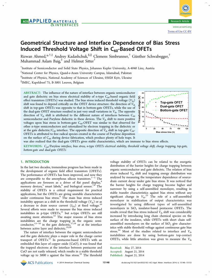
characteristics measured before bias stress, after 24h and125h of bias stress are presented in Figure 1. The Vth ofbottom-gate OFETs was shifted toward more positive voltage(from 20.7 to 34.6 V), while for top-gate OFETs the bias-stressresulted in the Vth shift in opposite direction to the left (from14.3 to 0.1 V) . In the case of dual-gate OFETs, only a smallshift in the Vth (from 11.5 to 8.5 V) was observed.
Figure 1. Transfer characteristics measured during the continuous biasstress of 125 h (a) bottom-gate top-contacts, (b) top-gate bottom-contacts, and (c) dual-gate OFETs.
ACS Applied Materials & Interfaces Research Article
dx.doi.org/10.1021/am5032192 | ACS Appl. Mater. Interfaces 2014, 6, 15148−1515315149
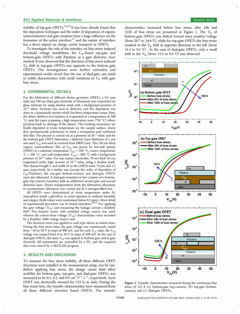
To quantify the bias stress instability in all three differentgeometrical-based OFETs, the Vth was extracted from thetransfer characteristics measured during the continuous biasstress time. For all three different geometrical structure basedOFETs, the change in the Vth during the continuous bias stresstime is presented in Figure 2. The Vth of bottom-gate OFET
was changed by 70%, the Vth of top-gate OFET changed by100%, while the Vth of dual-gate OFET changed by 20% only.The direction of change of Vth in dual-gate OFET was the sameas observed in top-gate OFETs. This means that bias stressphenomenon is related to top and bottom interface betweenC60 and Parylene, because all other device specifications are thesame. The improved stability observed in dual-gate OFETprovide an evidence that the mitigation of bias stress effectscaused by bottom-gate OFETs can be done by applying gatebias stress to the top-gate OFETs and vice versa. In dual-gateOFET, the bias stress induced instability at the top interface ishigher than the instability at the bottom interface caused bybias stress, because net direction of threshold voltage shift issimilar to the top-gate OFET.For practical application and device modeling, the stability of
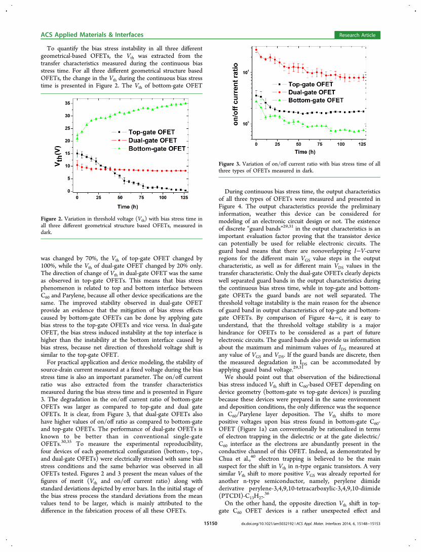
source-drain current measured at a fixed voltage during the biasstress time is also an important parameter. The on/off currentratio was also extracted from the transfer characteristicsmeasured during the bias stress time and is presented in Figure3. The degradation in the on/off current ratio of bottom-gateOFETs was larger as compared to top-gate and dual gateOFETs. It is clear, from Figure 3, that dual-gate OFETs alsohave higher values of on/off ratio as compared to bottom-gateand top-gate OFETs. The performance of dual-gate OFETs isknown to be better than in conventional single-gateOFETs.30,35 To measure the experimental reproducibility,four devices of each geometrical configuration (bottom-, top-,and dual-gate OFETs) were electrically stressed with same biasstress conditions and the same behavior was observed in allOFETs tested. Figures 2 and 3 present the mean values of thefigures of merit (Vth and on/off current ratio) along withstandard deviations depicted by error bars. In the initial stage ofthe bias stress process the standard deviations from the meanvalues tend to be larger, which is mainly attributed to thedifference in the fabrication process of all these OFETs.
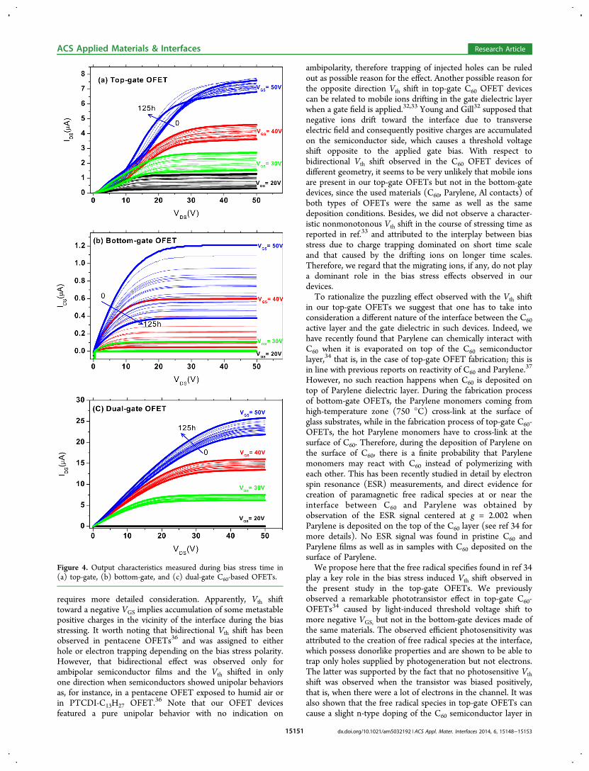
During continuous bias stress time, the output characteristicsof all three types of OFETs were measured and presented inFigure 4. The output characteristics provide the preliminaryinformation, weather this device can be considered formodeling of an electronic circuit design or not. The existenceof discrete “guard bands”29,31 in the output characteristics is animportant evaluation factor proving that the transistor devicecan potentially be used for reliable electronic circuits. Theguard band means that there are nonoverlapping I−V-curveregions for the different main VGS value steps in the outputcharacteristic, as well as for different main VDS values in thetransfer characteristic. Only the dual-gate OFETs clearly depictswell separated guard bands in the output characteristics duringthe continuous bias stress time, while in top-gate and bottom-gate OFETs the guard bands are not well separated. Thethreshold voltage instability is the main reason for the absenceof guard band in output characteristics of top-gate and bottom-gate OFETs. By comparison of Figure 4a−c, it is easy tounderstand, that the threshold voltage stability is a majorhindrance for OFETs to be considered as a part of futureelectronic circuits. The guard bands also provide us informationabout the maximum and minimum values of IDS measured atany value of VGS and VDS. If the guard bands are discrete, thenthe measured degradation in IDS can be accommodated byapplying guard band voltage.29,31
We should point out that observation of the bidirectionalbias stress induced Vth shift in C60-based OFET depending ondevice geometry (bottom-gate vs top-gate devices) is puzzlingbecause these devices were prepared in the same environmentand deposition conditions, the only difference was the sequencein C60/Parylene layer deposition. The Vth shifts to morepositive voltages upon bias stress found in bottom-gate C60-OFET (Figure 1a) can conventionally be rationalized in termsof electron trapping in the dielectric or at the gate dielectric/C60 interface as the electrons are abundantly present in theconductive channel of this OFET. Indeed, as demonstrated byChua et al.,40 electron trapping is believed to be the mainsuspect for the shift in Vth in n-type organic transistors. A verysimilar Vth shift to more positive VGS was already reported foranother n-type semiconductor, namely, perylene diimidederivative perylene-3,4,9,10-tetracarboxylic-3,4,9,10-diimide(PTCDI)-C13H27.
36
On the other hand, the opposite direction Vth shift in top-gate C60 OFET devices is a rather unexpected effect and
Figure 2. Variation in threshold voltage (Vth) with bias stress time inall three different geometrical structure based OFETs, measured indark.
Figure 3. Variation of on/off current ratio with bias stress time of allthree types of OFETs measured in dark.
ACS Applied Materials & Interfaces Research Article
dx.doi.org/10.1021/am5032192 | ACS Appl. Mater. Interfaces 2014, 6, 15148−1515315150
requires more detailed consideration. Apparently, Vth shifttoward a negative VGS implies accumulation of some metastablepositive charges in the vicinity of the interface during the biasstressing. It worth noting that bidirectional Vth shift has beenobserved in pentacene OFETs36 and was assigned to eitherhole or electron trapping depending on the bias stress polarity.However, that bidirectional effect was observed only forambipolar semiconductor films and the Vth shifted in onlyone direction when semiconductors showed unipolar behaviorsas, for instance, in a pentacene OFET exposed to humid air orin PTCDI-C13H27 OFET.36 Note that our OFET devicesfeatured a pure unipolar behavior with no indication on
ambipolarity, therefore trapping of injected holes can be ruledout as possible reason for the effect. Another possible reason forthe opposite direction Vth shift in top-gate C60 OFET devicescan be related to mobile ions drifting in the gate dielectric layerwhen a gate field is applied.32,33 Young and Gill32 supposed thatnegative ions drift toward the interface due to transverseelectric field and consequently positive charges are accumulatedon the semiconductor side, which causes a threshold voltageshift opposite to the applied gate bias. With respect tobidirectional Vth shift observed in the C60 OFET devices ofdifferent geometry, it seems to be very unlikely that mobile ionsare present in our top-gate OFETs but not in the bottom-gatedevices, since the used materials (C60, Parylene, Al contacts) ofboth types of OFETs were the same as well as the samedeposition conditions. Besides, we did not observe a character-istic nonmonotonous Vth shift in the course of stressing time asreported in ref.33 and attributed to the interplay between biasstress due to charge trapping dominated on short time scaleand that caused by the drifting ions on longer time scales.Therefore, we regard that the migrating ions, if any, do not playa dominant role in the bias stress effects observed in ourdevices.To rationalize the puzzling effect observed with the Vth shift
in our top-gate OFETs we suggest that one has to take intoconsideration a different nature of the interface between the C60active layer and the gate dielectric in such devices. Indeed, wehave recently found that Parylene can chemically interact withC60 when it is evaporated on top of the C60 semiconductorlayer,34 that is, in the case of top-gate OFET fabrication; this isin line with previous reports on reactivity of C60 and Parylene.
37
However, no such reaction happens when C60 is deposited ontop of Parylene dielectric layer. During the fabrication processof bottom-gate OFETs, the Parylene monomers coming fromhigh-temperature zone (750 °C) cross-link at the surface ofglass substrates, while in the fabrication process of top-gate C60-OFETs, the hot Parylene monomers have to cross-link at thesurface of C60. Therefore, during the deposition of Parylene onthe surface of C60, there is a finite probability that Parylenemonomers may react with C60 instead of polymerizing witheach other. This has been recently studied in detail by electronspin resonance (ESR) measurements, and direct evidence forcreation of paramagnetic free radical species at or near theinterface between C60 and Parylene was obtained byobservation of the ESR signal centered at g = 2.002 whenParylene is deposited on the top of the C60 layer (see ref 34 formore details). No ESR signal was found in pristine C60 andParylene films as well as in samples with C60 deposited on thesurface of Parylene.We propose here that the free radical specifies found in ref 34
play a key role in the bias stress induced Vth shift observed inthe present study in the top-gate OFETs. We previouslyobserved a remarkable phototransistor effect in top-gate C60-OFETs34 caused by light-induced threshold voltage shift tomore negative VGS, but not in the bottom-gate devices made ofthe same materials. The observed efficient photosensitivity wasattributed to the creation of free radical species at the interface,which possess donorlike properties and are shown to be able totrap only holes supplied by photogeneration but not electrons.The latter was supported by the fact that no photosensitive Vthshift was observed when the transistor was biased positively,that is, when there were a lot of electrons in the channel. It wasalso shown that the free radical species in top-gate OFETs cancause a slight n-type doping of the C60 semiconductor layer in
Figure 4. Output characteristics measured during bias stress time in(a) top-gate, (b) bottom-gate, and (c) dual-gate C60-based OFETs.
ACS Applied Materials & Interfaces Research Article
dx.doi.org/10.1021/am5032192 | ACS Appl. Mater. Interfaces 2014, 6, 15148−1515315151
dark, which resulted in a shift of Vth to more negativevoltages.34 In fact, the Vth in top-gate OFETs was somewhatsample-dependent that probably reflects variation of the freeradical concentration spontaneously created due to reactivity ofvapor deposited Parylene with C60. It is important to mentionthat mechanism of chemical doping in organic semiconductorsdiffers from the doping in conventional inorganic semi-conductors in that the yield of free charge-carriers dependssubstantially upon dopant concentration in a thresholdlikemanner and becomes feasible only at dopant concentrationlevel exceeding ∼0.3%.38,39 This is a direct consequence of two-steps doping process in organic semiconductors−first ioniza-tion of the dopant with donation of a charge carrier to the host,that is then followed by dissociation of such Coulombicallybound charge-carrier pair leading to creating a free chargecarrier.41 The recent molecular microelectrostatics calcula-tions38 showed that efficient dissociation of Coulombicallybound electron−hole pairs into free charge carriers in dopedorganic materials can occur at the doping level around 1%owing to dopant-concentration facilitated lowering the effectiveenergy barriers for the dissociation.We suggest that the free radical species present at the
interface are responsible for the observed bias stress induced Vthshift to more negative voltages in top-gate C60 OFET devices.Some free radicals can dope C60 semiconductors and those,which are not in the immediate proximity to C60 molecules,cannot dope the latter and remain neutral and therefore theycan serve as hole traps. Abundance of the hole traps in top-gateC60-OFET was shown recently34 and we have demonstratedthat they are responsible for the pronounced light-inducednegative Vth shift when sufficiently large negative VGS is applied(phototransistor effect). We believe that the latter phenomenonhas a similar origin as the Vth shift presently found upon thelong-term bias stressing of these OFETs. Indeed, one shouldtake into account that during the bias stress procedureperformed in our study a large VDS voltage (up to 50 V) isperiodically applied at various VGS values, including both smalland negative values. Therefore, the gate was in some momentsnegatively biased with respect to source or drain electrode. Thiscan facilitate tunneling of the holes generated by doping andinitially located at the ionized free radicals to the hole trapsdeeper inside the dielectric.As we mentioned above, the hole traps in top-gate C60-
OFETs have been shown34 to be constituted by neutral freeradicals though incidental hole traps inherent for Parylene alsoare not impossible. This eventually results in slow accumulationof positive charges trapped sufficiently deep inside of thedielectric and leads to considerable Vth shift to the left (Figure1b). In other words the observed effect could be explained interms of doping enhanced by electric field because dissociationof electron−hole pairs into free carriers is enhanced by bothtemperature and electric field.39 On the other hand, the abovefree radicals cannot trap electrons as shown before.34 Electronscan be trapped when gate is positively biased only by some sortof incidental traps inherent for Parylene independent of theway of its deposition. In top-gate devices hole traps due to freeradicals likely overcompensate the conventional incidentalelectron traps, therefore hole trapping prevails over the electrontrapping and, as result, Vth shifts left. We should also note thatdue to relatively small concentration of the free radicals inimmediate proximity to the C60 layer, majority of dopant-induced electron−hole pairs are expected to remain Coulombi-cally bound since their dissociation yield into free charge-
carriers is low. Indeed, the Vth in unstressed top-gate OFETstends to be somewhat shifted to the left with respect to that inbottom-gate devices (cf. Figure 1a,b) that could mean someslight n-doping in the former case.Finally, the very small Vth shift in dual-gate OFETs can be
explained as most probably combined bidirectional effects fromtop-gate and bottom-gate, which almost cancel each other.Since the stress-induced Vth shift is relatively stronger in top-gate device, this can explain why Vth in dual-gate OFET issimilarly slightly shifted to the left (Figure 1c). More detailabout the dual-gate operation can be found in a recent article.35
4. CONCLUSIONIn summary, the bias stress induced instabilities in C60-basedtop-gate, bottom-gate, and dual-gate OFETs, with Parylene as agate dielectric, were studied. It was observed that the directionof bias stress induced threshold voltage shift in top-gate OFETswas opposite to the bottom-gate devices. The Vth shift to morepositive voltages in bottom-gate C60 OFET was similar to thatreported in literature for other n-type semiconductors and canconventionally be rationalized in terms of electron trapping inthe dielectric or at the gate dielectric/C60 interface. On theother hand, the opposite direction of Vth shift upon bias stressfound in C60 top-gate OFETs is attributed to the modificationof the semiconductor/dielectric interface occurring duringParylene deposition on the surface of C60. We suggest thatcreation of free radicals recently detected by EPR study in top-gate devices,34 which constitute abundance of hole traps at ornear the interface, plays a key role in the Vth shift to morenegative voltages upon bias stress in the dark. The bias stresseffect in dual gate OFETs was also studied, and it was shownthat the use of dual-gate can result in stable characteristics withsmall variations in threshold voltage.
■ AUTHOR INFORMATIONCorresponding Author*E-mail: [email protected] or [email protected] authors declare no competing financial interest.
■ ACKNOWLEDGMENTSThe financial support from Austrian Science Fund (FWF):P25154−N20, the European Research Council by Grant No.320680 (EPOS CRYSTALLI) and by the NAS of Ukraine viathe program of fundamental research on nanophysics (ProjectNo. 1/14-H-23K) are acknowledged.
■ REFERENCES(1) Stutzmann, N. S.; Smits, E.; Wondergem, H.; Tanase, C.; Blom,P.; Smith, P.; de Leeuw, D. Organic Thin-film Electronics fromVitreous Solution-Processed Rubrene Hypereutectics. Nat. Mater.2005, 4, 601−606.(2) Nigam, A.; Schwabegger, G.; Ullah, M.; Ahmed, R.; Fishchuk, I.I.; Kadashchuk, A.; Simbrunner, C.; Sitter, H.; Premaratne, M.; Rao, V.R. Strain Induced Anisotropic Effect on Electron Mobility in C60Based Organic Field Effect Transistors. Appl. Phys. Lett. 2012, 101,083305−083308.(3) Nigam, A.; Schwabegger, G.; Ullah, M.; Ahmed, R.; Fishchuk, I.I.; Kadashchuk, A.; Simbrunner, C.; Sitter, H.; Premaratne, M.; Rao, V.R. Anisotropic Strain Effect on Electron Transport in C60 OrganicField Effect transistors. MRS Symp. Proc. 2013, 1501, 05−07.(4) Zhou, L. S.; Wanga, A.; Wu, S. C.; Sun, J.; Park, S.; Jackson, T. N.All-Organic Active Matrix Flexible Display. Appl. Phys. Lett. 2006, 88,083502−083504.
ACS Applied Materials & Interfaces Research Article
dx.doi.org/10.1021/am5032192 | ACS Appl. Mater. Interfaces 2014, 6, 15148−1515315152
(5) Liu, X.; Zhao, H.; Dong, G.; Duan, L.; Li, D.; Wang, L.; Qiu, Y.Multifunctional Organic Phototransistor-Based Nonvolatile MemoryAchieved by UV/Ozone Treatment of the Ta2O5 Gate Dielectric. ACSAppl. Mater. Interfaces 2014, 6, 8337−8344.(6) Rotzoll, R.; Mohapatra, S.; Olariu, V.; Wenz, R.; Grigas, M.;Dimmler, K.; Shchekin, O.; Dodabalapur, A. Radio FrequencyRectifiers Based on Organic Thin-Film Transistors. Appl. Phys. Lett.2006, 88, 123502−504.(7) Crone, B. K.; Dodabalapur, A.; Sarpeshkar, R.; Gelperin, A.; Katz,H. E.; Bao, Z. Organic Oscillator and Adaptive Amplifier Circuits forChemical Vapor Sensing. J. Appl. Phys. 2002, 91, 10140−10146.(8) Torsi, L.; Marinelli, F.; Angione, M. D.; Dellaquila, A.; Cioffi, N.;de Giglio, E.; Sabbatini, L. Contact Effects in Organic Thin-filmTransistor Sensors. Org. Electron. 2009, 10, 233−239.(9) Osedach, T. P.; Zhao, N.; Andrew, T. L.; Brown, P. R.; Wanger,D. D.; Strasfeld, D. B.; Chang, L. Y.; Bawendi, M. G.; Bulovic, V. Bias-Stress Effect in 1,2-Ethanedithiol-Treated PbS Quantum Dot Field-Effect Transistors. ACS Nano 2011, 6, 3121−3127.(10) Fomani, A. A.; Nathan, A. Metastability Mechanisms in ThinFilm Transistors Quantitatively Resolved Using Post-Stress Relaxationof Threshold Voltage. J. Appl. Phys. 2011, 109, 084521−084526.(11) Salleo, A.; Street, R. A. Light-Induced Bias Stress Reversal inPolyfluorene Thin-Film Transistors. J. Appl. Phys. 2003, 94, 471−479.(12) Sirringhaus, H. Reliability of Organic Field-Effect Transistors.Adv. Mater. 2009, 39, 3859−3873.(13) Tello, M.; Chiesa, M.; Duffy, C. M.; Sirringhaus, H. ChargeTrapping in Intergrain Regions of Pentacene Thin Film Transistors.Adv. Funct. Mater. 2008, 18, 3907−3913.(14) Mathijssen, S. G. J.; Colle, M.; Mank, A. J. G.; Kemerink, M.;Bobbert, P. A.; de Leeuw, D. M. Scanning Kelvin Probe Microscopyon Organic Field-Effect Transistors During Gate Bias Stress. Appl.Phys. Lett. 2007, 90, 192104−192106.(15) Yogev, S.; Matsubara, R.; Nakamura, M.; Rosenwaks, Y. LocalCharge Accumulation and Trapping in Grain Boundaries of PentaceneThin Film Transistors. Org. Electron. 2010, 11, 1729−1735.(16) Puntambekar, K. P.; Pesavento, P. V.; Frisbie, C. D. SurfacePotential Profiling and Contact Resistance Measurements onOperating Pentacene Thin-film Transistors by Kelvin Probe ForceMicroscopy. Appl. Phys. Lett. 2003, 83, 5539−5541.(17) Ng, T. N.; Marohn, J. A. Comparing the Kinetics of Bias Stressin Organic Field-effect Transistors with Different Dielectric Interfaces.J. Appl. Phys. 2006, 100, 084505−084510.(18) Mathijssen, S. G. J.; Kemerink, M.; Sharma, A.; Colle, M.;Bobbert, P. A.; Janssen, R. A. J.; de Leeuw, D. M. Charge Trapping atthe Dielectric of Organic Transistors Visualized in Real Time andSpace. Adv. Mater. 2008, 20, 975−979.(19) Katz, H. E.; Kloc, C.; Sundar, V.; Zaumseil, J.; Briseno, A. L.;Bao, Z. Field-Effect Transistors Made from Macroscopic SingleCrystals of Tetracene and Related Semiconductors on PolymerDielectrics. J. Mater. Res. 2004, 19, 1995−1998.(20) Klauk, H.; Halik, M.; Zschieschang, U.; Schmid, G.; Radlik, W.High-Mobility Polymer Gate Dielectric Pentacene Thin FilmTransistors. J. Appl. Phys. 2002, 92, 5259−5263.(21) Dong, H.; Jiang, L.; Hu, W. Interface Engineering for High-Performance Organic Field-Effect Transistors. Phys. Chem. Chem. Phys.2012, 14, 14165−14180.(22) Nie, G.; Peng, J.; Lan, L.; Xu, R.; Zou, J.; Cao, Y. Tuning onThreshold Voltage of Organic Field-Effect Transistor with a CopperOxide Layer. Org. Electron. 2011, 12, 429−434.(23) Miyadera, T.; Wang, S. D.; Minari, T.; Tsukagoshi, K.; Aoyagi,Y. Charge Trapping Induced Current Instability in Pentacene ThinFilm Transistors: Trapping Barrier and Effect of Surface Treatment.Appl. Phys. Lett. 2008, 93, 033304−033306.(24) Suemori, K.; Uemura, S.; Yoshida, M.; Hoshino, S.; Takada, N.;Kodzasa, T.; Kamata, T. Threshold Voltage Stability of Organic Field-effect Transistors for Various Chemical Species in the InsulatorSurface. Appl. Phys. Lett. 2007, 91, 192112−192114.
(25) Diallo, K.; Erouel, M.; Tardy, J. Stability of Pentacene TopGated Thin Film Transistors. Appl. Phys. Lett. 2007, 91, 183508−183510.(26) Hwang, D. K.; Fuentes-Hernandez, C.; Kim, J.; Potscavage, W.J., Jr.; Kim, S. J.; Kippelen, B. Top-Gate Organic Field-EffectTransistors with High Environmental and Operational Stability. Adv.Mater. 2011, 23, 1293−1298.(27) Veres, J.; Ogier, S.; Lloyd, G.; de Leeuw, D. Gate Insulators inOrganic Field-Effect Transistors. Chem. Mater. 2004, 16, 4543−4555.(28) Schwabegger, G.; Ullah, M.; Irimia-Vladu, M.; Reisinge, M.;Kanbur, Y.; Ahmed, R.; Stadler, P.; Bauer, S.; Sariciftci, N. S.; Sitter, H.High Mobility, Low Voltage Operating C60 Based N-Type OrganicField Effect Transistors. Synth. Met. 2011, 161, 2058−2062.(29) Ahmed, R.; Sams, M.; Simbrunner, C.; Ullah, M.; Rehman, K.;Schwabegger, G.; Sitter, H.; Ostermann, T. Reproducibility andStability of C60 Based Organic Field Effect Transistor. Synth. Met.2012, 161, 2562−2565.(30) Maddalena, F.; Spijkman, M.; Brondijk, J. J.; Fonteijn, P.;Brouwer, F.; Hummelen, J. C.; de Leeuw, D. M.; Blom, P. W. M.;Boer, B. Device Characteristics of Polymer Dual-Gate Field-EffectTransistors. Org. Electron. 2008, 9, 839−846.(31) Islam, A. E.; Alam, M. A. On the Possibility of Degradation-FreeField Effect Transistors. Appl. Phys. Lett. 2008, 92, 173504.(32) Young, N. D.; Gill, A. Water-Related Instability in TFTsFormed Using Deposited Gate Oxides. Semicond. Sci. Technol. 1992,7, 1103−1108.(33) Zilker, S. J.; Detcheverry, C.; Cantatore, E.; de Leeuw, D. M.Bias Stress in Organic Thin-Film Transistors and Logic Gates. Appl.Phys. Lett. 2001, 79, 1124−1126.(34) Ahmed, R.; Kadashchuk, A.; Simbrunner, C.; Schwabegger, G.;Havlicek, M.; Głowacki, E.; Sariciftci, N. S.; Baig, M. A.; Sitter, H.Photosensitivity of Top Gate C60 Based OFETs: PotentialApplications for High Efficiency Organic Photodetector. Org. Electron.2014, 15, 175−181.(35) Spijkman, M.-J.; Myny, K.; Smits, E. C. P.; Heremans, P.; Blom,P. W. M.; de Leeuw, D. M. Dual-Gate Thin-film Transistors,Integrated Circuits and Sensors. Adv. Mater. 2011, 23, 3231−2342.(36) Debucquoy, M.; Rockele, M.; Genoe, J.; Gelinck, G. H.;Heremans, P. Charge Trapping in Organic Transistor Memories: onthe Role of Electrons and Holes. Org. Electron. 2009, 10, 1252−1258.(37) Loy, D. A.; Assink, R. A. Synthesis of a Fullerene C60-p-XylyleneCopolymer. J. Am. Chem. Soc. 1992, 114, 3977−3978.(38) Mityashin, A.; Olivier, Y.; Regemorter, T. V.; Rolin, C.; Verlaak,S.; Martinelli, N.; Beljonne, D.; Cornil, J.; Genoe, J.; Heremans, P.Unraveling the Mechanism of Molecular Doping in OrganicSemiconductors. Adv. Mater. 2012, 24, 1535−1539.(39) Lussem, B.; Riede, M.; Leo, K. Doping of Organic Semi-conductors. Phys. Status Solidi A 2013, 210, 9−43.(40) Chua, L. L.; Zaumseil, J.; Chang, J. F.; Ou, E.; Ho, P.;Sirringhaus, H.; Friend, R. H. General Observation of N-type Field-Effect Behaviour in Organic Semiconductors. Nature 2005, 434, 194−199.(41) Pope, M.; Swenberg, C. E. Electronic Processes in Organic Crystalsand Polymers, 2nd ed.; Oxford University Press: New York, 1999.
ACS Applied Materials & Interfaces Research Article
dx.doi.org/10.1021/am5032192 | ACS Appl. Mater. Interfaces 2014, 6, 15148−1515315153