
Fulltext PDF 6,4 MB - HZDR
99
-
Upload
khangminh22 -
Category
Documents
-
view
0 -
download
0
Transcript of Fulltext PDF 6,4 MB - HZDR


Content
1. Introduction 4
2. Scientific contributions
On the Mechanism of Carbon-Induced Doping in Implanted Silicon W. Skorupa, M. Voelskow, K. Schmalz, G. Morgenstern, arid P. Gaworzewiski 7
Iron Gettering by MeV-Carbon Implantation W. Skorupa, R. Kögler, M. Voelskow, and K. Schmalz 9
Formation of Buried (Fel,&ox)Si2 Layers in (100)Si by Ion Beam Synthesis D. Panknin, E. Wieser, W. Skorupa, G. Querner, H. Vöhse, J. Albrecht, and W. Henrion 10
Investigation of Pulsed Ion Beam Induced Arnorphization/Crystallization of Silicon for Irradiation with ~ r + Ions of 3.8 MeV R. Kögler, V. Heera, W. Skorupa, E. Glaser, T. ~achmann; and D. Rück 12
Cornputerprogram for Calculating Reflectivities of Multi-Layer-Systems Th. Henkel and V. Heera 14
A Formuia for Estimating IBIECIIBIIA-rates on Silicon V. Heera 16
High Current FIB System for Micromechanics Application L. Bischoff, E. Hesse, G. Hofmann, W. Probst, B. Schmidt, and J. Teichert 18
Preparation of the IMSA-100 for Ion Beam Synthesis Pusposes L. Bischoff and J. Teichert
Development of a Cobalt Liquid Meta1 Ion Source E. Hesse and J. Teichert 22
Two Concentric Emission Bundles Prom a Lithium Liquid ibletal Ion Source E. Hesse and F.K. Naehring 24
Investigations of the Electrochemical Etch Stop on Silicon Wsing KOH B. Schmidt 25
Electrochemical Etch Stsp Behaviour on Ion Implanted Silicon pn-Jtnnctions B. Schmidt 24
A Measurenient System for Studying Etectrochemicat Field Effect Ion Saralstfivity MT, Pham, W. Taubert, and M, Blirger

An Approach to the Cross Sensitivity of the Ion Sensing Membranes M.T. Pham and S. Howitz 3 1
ISFETs with Controlled Gate Membrane Opening M.T. Pham and S. Howitz 3 3
Ion Beam Modified Insulator Layers as ISFET Membranes,for Heavy Meta1 Ion Detection J. Hüller, W. Hoffmann, and M.T. Pham 3 5
Differential Measurements with ISFETs in Microfluid Systems M.T. Pham and S. Howitz 3 7
Cooperative Project "Fluidic- ISFET- Microsystem" S. Howitz and M.T. Pham 3 9
Repth Profiles of C, N, and 0 on Carbon Coated Steel Surfaees Made by IBAD A. Kolitzsch, E. Hentschel, and E. Richter 42
High Dose Implantation of Aluminium into Iron -
H. Reuther, 0. Nikolov, S. Krujer , R. A. Brand, and W. Keune
A Magnetron Source for Ion Implantation H. Reuther
Modelling of Implantation-Induced Transient Diffusion and Electrical Activation of Boron in Crystalline Silicon during Post-Implantation Annealing H. U. Jäger 5 0
Computer Simulation of Channeling Implantation of Phosphoms into Silicon M. Posselt 53
Dielectric Theory of Electronic Energy Loss in a Homogeneous Electron Gas: Effect of First Order Polarization R. Mathar 5 6
Molecuiar Dynamics Simulations of Defect Formation by Low-Energy Ion Bombardement D. Stock and K.H. Weinig 59
Thermalization in ColIision Cascades Investigated by MolecuIar Dynamics Calculations K.-H. Heinig asd D. Stock 6 1
Compression Waves Induced in Si by ~ i w - ~ n e r ~ ~ Ions - ft Molecular Dynmics SimuIation K.-H. Heinig and D. Stoi;k 63
Mofecufar Dynämicii (MD) Simulations f GIUD Experiments 64

The Diffractometer of the RCR at the Rez Reactor A. Mücklich, M. Betzl, P. Reichel, and W. Boede 67
Neutron Diffraction Analysis of Substructures in Polycrystalline Materials P. Klimanek, T. Kschidock, A. Mücklich, P, Lukas, P. Mikula, and M. Vrana 69
Study of Hardening Portland Cement Paste by Small-Angle Neutron Scattering F. Eichhorn, F. Häußler, and H. Baumbach 72
Studies of SrxBal-xNb206 Mixed Crystals by Neutron Diffraction at Temperatures between 15 K and 293 K F, Prokert and B.N. Savenko 74
The Neutron Time-of-Flight Diffractometer NSHR at IBR-2 in Dubna . J. Heinitz, K. Ullemeyer, and K. Waither 76
7.25 GHz ECR Source for Highly Charged Ions R. Hentschel, H. Tyrroff, L. Friedrich, E. Huttel, and L. Wiss 79
Improvement of the Experimental Possibilities at the 2 MV Van de GraaiT Accelerator W. Bürger, M. Friedrich, R. Grötzschel, C. Neelmeijer, and 5. Turuc 82
Status Report of the 3 MV Tandetron M. Friedrkh, S. Langer, S. Turuc, and E. Wieser 82
Developments for the Acceleratot Control and Stabilizing Systems W. Bürger 84
3. List of publications, conference contributions, and seminary lectures S 5
4. Personnel 98

In troduction
On January 1, 1992 the Research Center Rossendorf started its work in succession of the former Central Institute of Nuclear Research. The Institute of Ion Beam Physics and Materials Research, founded in 1991, is now one of the five scientific institutes of the Research Center. This transformation was connected with two important consequences for our institute. The permanent staff of the institute was reduced to 78 employees, among it 32 scientists. But, as a remarkable success of the first year under the new status we can report that at the end of 1992 the man power of the institute was eompleted by 15 positions within the framework of additionally funded projects and by 8 doctoral fellowsimips. Therefore a csntinuation of all branches of the scientific Programme, reported in the status report 1991, was possible. These topics are:
- Modification of Semiconductors and Microbezm Facility - Application of Ion Beams to Sensors - Modification of Metals and Other Materials - Theory of Ion-Beam Induced Processes in Solids - Fundarnentals of Ion-Solid Interaction and Ion Beam Analysis - Structure Studies Using X-Rays and Neutron Scattering.
A much more serious problem was the missing permission to operate our ion beam accelerators. Only from November 1992 experiments using the implanta-s were possible. The restart of the electrostatic accelerators is expected for February 1993. Therefore the scientific output of the experimental departments was limited to the evaluation of data available from the foregoing year. In some special cases we were able to use beam time in external laboratories. With this respect we gratefully acknowledge the help of the accelerator laboratory of TU and LMU Munich (W. Assmann, A. Weidinger), of the GSI Darmstadt (D. Rück), and of the Technical University Chemnitz.
The following introductory review of some main results obtained in the research fields mentioned above proves that also this complimted year may be considered as an important step fonvards in the development of the new institute to an efficient Center for the use of ion beam techniques in materiais research.
During the last year the activities in the field "'Ion Beam Modification of Semiconductors md Miczobeam Facility" were mainiy concentrated on the investigation of samplcs aiready prepared in 1991. For the first time, ian beam synthesis was used to study the formatiorv of buried Fe-Co silicide faytsls. Lliis was done in order to continue the recent work on the formation of
with respect to a possible band gap engineering OE the semiconducting ß-FeSi2 phasa
The investigation OE prsximity &ttering oE iron by MeV-crirbon implantation was also ntinued. Beside the gettering behavisur doping effects due to carbon were studied.
xperimea&lly detemined rates of ion beam indued epitaxial crystalkzation (IERIC) tvere campared with the rrefuits rtf ciomputer mdefling. Concerning tRe basic mechanism shis mmprisun favoorr; tha effect of dnf; defect difiFusion tcr the interface.

First experiments carried out at a RFQ accelerator of the GSI Darmstadt led to interesting results on the influence of pulsed ion irradiation on the IBIEC process. The activities at the microbeam facility were mainly devoted to an overall testing of the apparatus. Final test experiments at a lithium-ion source were perfonned and a Co-Nd alloy was tested in order to get a Co beam from a liquid metai ion source.
The work of the department of "Application of Ion Beams for Sensors" can be devided into the three topics radiation Sensors, chernical microsensors and micromechanics. One main task was the development of special processes for the fabrication of HP-Ge detectors like the formation of n' layers by phosphorus implantation, the preparation of amorphous germanium layers for passivation and contacts by sputtering and the investigation of the growth of germanium oxide during chemical preparation and annealing. The investigation of ion beam synthesis of chalcogenide glasses and of their sensibilization for the detection of heavy metals by ion sensitive field effect-lransistors (ISFET) was continued. A very important event was the Start of a cew project with the aim to develop an integrated microsystem of ISFET and microfluidic components fix the dynamical measurement of ion concentrations in liquids. The activities in the field of micromechanics were devoted to the realization of sub-pm silicon membranes by anisotropic etching and the development of an electrostatic valve in silicon technique.
Due to the lack of ion beams the work of the department "Ion Beam Modification of Metals and Other Materials" was mainly concentrated on the improvement of the
'*
experimental equipment. The construction of the apparatus for ion beam assisted deposition (IBAD) was completed and the main components of the new implanter "Scanibal" were succe%sfully tested. Important improvements were obtained considering the equipment for materials testing. A profilometer, a scratch tester, an ultramicrohardness tester and the reconstructed wear tester were taken into operation. The investigations with the aim to use ultrasonic surface waves in order to study thin film properties were continued with an improved detection System by first experiments on TiN layers on steel. The evaluation of IBAD experiments from 1991 where hard and wear resistant carbon layers were formed by Cf implantation into a growing carbsn layer led to a deeper insight into the acting mechanisrn.
The activities of our group "Theory of Ion Beam Induced Processes in Solids" wwere continued with investigations on the interdction of ion beams with materials during implantation and on subsequent re-ordering processes including the development taf new theoretical methods as we1I as collaboration with the experimental groups. A f e ~ extensive Computer codes were devdoped to simulate (i) the s'fowing down of ions in crystaIline targets in the framework of the binary collision approxirnation, (ii) the sllowing down uf low-energy ions by rnolecular dynamic ~;ilculations, and (Ei) tb cnugkd diffusion of impurities and point defecrts in salids, In the last year the pliysid probims treated in this way were:

(i) Channeling effects in high and medium energy implantation into silicon, (ii) MD calculations of the thermalization and defect generation in collision cascades
as well as simulations of gamma-ray induced Doppler broadened (GRID) spectra, (iii) implantation induced transient enhanced diffusion and electrical activation of
boron in crystalline silicon during post-implantation annealing.
In 1992 the situation for the department "Fundamentals of Ion-Solid Interactions and Ion Beam Analysis" was especially difficult due to the missing permission to operate the accelerators. Therefore the activities were concentrated on apparative work originally scheduled for a Iater date. Thus a new beamline for hydrogen depth profiling by resonance reactions ( 1 5 ~ , 1 9 ~ beams) was designed and assembled. It allows, by a combination of beam sweeping and focusing, a homogeneous irradiation of large area spots on the target in order to minimize hydrogen redistribution. The reconstruction of the'ERDA scattering chamber was completed bly the installation of the PC based multiparameter data acquisition system for the Bragg ionization charnber and the dE-E-SSD telescope. This dedicated telescope for recoil atoms of hydrogen isotopes could be tested at the ERDA facility of the Munich MP tandam. At the 2 MV Van de Graaff accelerator the installation of the switching rnagnet and the differentially pumped beam line to the UHV scattering chamber was finished.
The department for "Accelerator Technique" used this yeat mainly for technical improvements of the 5 MV tandem accelerator and here especially for the automatic control of ion source, for the stabilization of the acceleration voltage and for upgrading the radiation safety equiprnent. This gives the possibility of routine operation with reduced staff. Extensive work was done in order to reconstruct parts of the tandem building for the instaliatisn of the new 3 MV tandetron which is expected for spring 1993.
The most important task for the department "Structure Studies Using X-Ray and Neutton Scattering" was the transfer of neutron scattering equipment from our closed research reactor t s external reactor facilities and the extension of the X-ray laboratory in our institute incfuding the installation of new equipment. A multipurpose neutron diffractometer was installed and tested at the research reactor in Rez near Prague. From autumn 1992 it is in cooperative use together with the TU MA Freiberg for texture stuciies of afloys, with the Center for Geo Research Potsdam for geological texture investigations and with the TU Chemnitz for structure investigations af melts. The preparation of an improved double cryslal neutron diffractorneter for fundamental studies and smdl-angle scattering experiments for its transfer to the reactor of the Hahn- Meitnes-Inst2tu& in BerIin was finished. The time-of-ffight neutron diffractorneter at the pulsed reactor of the Joint Institute for Nucfear Research in Dubna was in suecessful operation. Our small group in Dubna investigated about 50 sampfm Eom the universities in Gottingen, Rostock, Chemnitz and Berkeley, ftom the RVVTH Aachen and the Center of Geo Research Potsdam. Texture problern of geofogia1 sampies were the dominating subject of tfiese studies. By wur presence in Dubna. it was also pcsssibIe to use the smail-angle scaftering equipment MURN and ihe singfe-crptal dif%l-actometer DN-2.

On the Mechanism of Carbon-induced Doping in Implanted Silicon
W. Skorupa, M. Voelskow, K. Schmalz', G. Morgenstern' and P. Gaworzewskil,
'Institute for Semiconductor Physics, PO3 409, 0-1200 Frankfurt, Germany
Recently, it was shown that the carbon induced donor formation has a maximum concentration at a dose of 1015 cm-2 [I]. On the other hand, a dose of 1013 cmS does not show any doping effect. This was confirmed by our new results after 5 MeV cclrbon implantation in that donor formation sets in at 3x10¹³ ~ r n - ~ and the electrical activation grows increasing the carbon dose to 1015cm-2 [2]. For this dose the carrier concentration profile of a CZ- and a FZ-wafer is shown in Fig. 1. The profile of the CZ-wafer shows a Gaussian-like shape with a projected range of 4.9 Pm. The maxi- mum canier concentration is 2x1016 cm" subtracting the basic concentration of the wafer. This results, comparing with the maximum atomic concentration measured by SIMS (see Fig.2) of 10'' ~ m - ~ , in an electrical activation of only 0.2 %. The carrier concentration of the FZ-wafer is distinctly lower and shows a broad distribution. The . maximum lies also at the projected range of the other curve, but this profile is further characterised by a broad tail towards the surface. The electrical activation is distinctly lower than for the CZ-material (0.002 %).
1017
- ; U 1016 U
Z 0 2 1d5 Z W U Fig. 1: Z
U Camer concentration profiles evaluated 10 '~ from spreadieg resistance measurements s
a afier carbon implantation and amealing a Q U
of Cmchralski-grswn (GZ)- and Floar
i d 3 zone-grown (FZ)-sipicon wafers, 0 4.0 2.0 3 0 1.0 5.0 6 0 70
DEPTH [pm]
The SIMS measurements of the atornic profiles after implantation at 5 MeV with a d0s.e of i015cm-2 showed exactly the Same carbon profiles independently on the material type - CZ or FZ - or the annealmg state - as implanted or anneafed at atornic profiles for CZ- and FZ-material after anriealing are s suggests, the distinctly higher activation In the CZ-matefial mtrst higher oxygen eontent. The profile k.61 rneasured in FZ-mat~rial dire is not caused by my differente of the mtiasureabIe carbon conce Into aacount that the detection lirnit ofSSlMS .fgr cartson is abou the reason fw the see~~ingly higher carbon Ievef of about E is not yet cIear,

I2c+, SMeV, 1075m-2 1000QC, l h , N 2
- c z
Pig.2: SIMS proiiles of the carbon concentration after carbon implantation and annea1'ing of Czochralski- grown (CZ)- and Float wne- grown (FZ)-silicon wafers.
OEPTH [ ~ m ]
The question arises if the introduction of implantation darnage alone in CZ- as well as in FZ-silicori material leads also to a doping effect, especiam in the presence of oxygen. For Ithis end we implanted both Si-material types with 12.5 MeV silicon ions with the Same doses as carbon. The choice of the implantation energies - 5 MeV for carbon and 312.5 MeV for silicon - was made to ensure nearly the same projected range of about 5 Pm. Moreouer, this leads to a comparable energy deposition into electronic anid nuclear processes in the Same depth regions. In contrast to the results after carbon implantation and annealing at l W C , no doping effect was found in the wafers implanted with silicon ions independently on the dose (3x10'3-3x10'S cmS) or the oxygen content of the wafers (1016 ~ m - ~ for FZ, 10" cmm3 for CZ). This points emphatidly to the fact, that the carbon induced doping effect is first of all related to carbon and not to radiation damage. alone, or a combination of damage and oxygen. Nevertheless, compadng the results after carbon implantation in FZ- and CZ- material, oxygen plays an essential role in that the carbon induced dopant activation is favoured in oxy.gm-hch CZ-material,
Refe~ences [ll W. Skonipa, R. Kijgfer, M, VoeIskow, E. Sc~malz, G. Morgenstcm and P. Gaworzewski,
Nd. h t r = Meth, B68 (1992) 408, 123 12- Skompa, R. Kögkr, K. Schmalz, P. Gaworzewski, G. Morgenstern and H. Syhre
NI&, ilnstr, Meth. B [to be pubXished)

Iron Gettering by MeV-carbon Implantation
W. Skorupa, R. Kögler, M. Voelskow, K. Schmalz1, G. Morgenstern1 and P. Gaworzewski',
'Institute for Semiconductor Physics, POB 409, 0-1200 Frankfurt, Germany
The gettering efficiency for iron of a buried carbon-rich layer formed by 10 MeV- carbon implantation with doses in the range of 1014-1016 cm-2 and annealing was in- vestigated. Iron was additionally introduced into the back of the silicon wafers by im- plantation with an energy of 330 keV and doses of 1e2 ~ m - ~ and 1013 ~ m - ~ . Gettering of Fe sets in at a carbon dose of 1014 cmS and is completed at the surface of the wafer for a carbon dose of 1016 cmq, both for the highest investigated iron dose of 1013 cm-2 [I]. Moreover, a through-tbwafer inspecthn of the iron distribution was made [2]. In Fig. 1 the depth profide of the FeB-pair concentration as revealed by DLTS for a wafer with a thickness of about 300 nm is shown for an iron dose of 1013 cm-* . The FeB-pair formation takes place at about 150°C that means in the cooling down phase of the annealing step. Due to the high diffusion coefficient, at the temperature of l W C , interstitial iron atoms are homogeneously distributed throughout the wafer. Gettering by carbon leads to a strong l o w e ~ g of the iron concentration near to the surface up to about three orders of magnitude. For the highest carbon dose of 1e6 ~ r n - ~ the iron content is lowered in the whole wafer. This points to iron diffision toward the carbon implanted layer during the cooling-down phase. For the case of the highest carbon dose of 1016 cm-' iron gettering at 1000°C seems to be bncerned with the formation of iron- carbon-complexes.
I 1 I
1
CARBON DOSE V not implankd
.o W"+ C - 2
0 1016m-2 Fig, 1: Depth prafile of the d e q tevd density of iron-boron-pairs in silicon wafers perfonned
Refe~ences: [l] W, Skonipa, R. KogIer, M. Voelskow, K. Schmlz, G. Morgenstern wd P, G ~ w o ~ w s f c i
NueL Instr. Meth. B 68 (1992) 408 E21 W. Skorupa, R- Kögier, K, Schmalz, G , Morgenstern and H. SyhZe
b c . 1X. ht. Conf. Ion Implaatation Technalogy, Gain~vifle (USA), Sept, 21-24, Hscl, Instr. M&. B ($0 'be published)

Formation of Buried (Fe,-,Co,)Si, Layers in (100) Si by Ion Beam Synthesis
D. Panknin, E. Wieser, W. Skorupa, G. Quernerl, H. Vöhse2, J. ~ l b r e c h t ~ and W Hennon3
'Technical University Dresden Institute Fresenius Dresden
3Hahn-Meitner-Tnstitute Berlin
FeSi, exists in two crystalline modifications: The semiconducting low temperature ß- phase arid the metallic high temperature a-phase. The transition from 6- to a-FeSi, occurs at 967°C. The formation of a buried iron silicide layer into Si by ion bearn synthesis is reported in Refs. [I-31. The possibility of changing the properties of semiconducting P-FeSi, by addition of a third element is of interest as it may influence the band gap energy as well as the epitaxial growth of the buried silicide. In Refs.' 14-61 results are summarized concming the ion beam synthesis of (Fe, Co)Si, in (100) Si. For these investigations Fe (4xl0l7 cm-2 with 300 keV at 350°C) and Co (5x1016 cm-2 and IxlOl7 cm-2 with 180 keV at 350°C) were implanted. For a first series, samples were annealed at 850°C before the Co implantation resulting in a well defined layer of ß-FeSi,. For a second series, Co was implanted directly following the Fe irnplantation. After the Co implantation all samples were annealed at temperatures between 600°C and 1050°C in N2 atmosphere. The phase composition of the (Fe,-&~&ji, system is aietermined by X-ray diffraction [4]. In Fig. 1 the intensities of selected diffraction peaks in dependence on the pbst- implantation annealing temperature are shown for x=0.2. In the as-implanted state as wdl as after post-implantation annding below 850°C only peaks of the $-Fes&

structure are observed. This proves that the polycrystalline semiconducting structure is preserved after the Co implantation. Comparing to pure FeSi, the temperature of the 0- to a-transition is shifted to lower temperatures in dependence on the Co content. The temperature shift of the phase transition is more pronounced for samples without intermediate annealing. The depth distribution of Fe and Co, measured by Auger Electron Spectrometry, is shown in Fig. 2 after post-implantation annealing at 850°C [5,6].
Fig. 2: Auger depth profiles of Fe and Co after annealing at 850°C (4x10" Fe cmv2 + 1x10'~ Co cni2; with intermediate annealing)
For the sample with intermediate annealing a nearly homogeneous distribution of both metals is observed. In this region the stoichiometric ratio Si/(Fe+Co) is near to the stoichiometric ratio Si/Fe of pure ß-FeSi, [I]. This means that the Co atoms substitute Fe in the 6-FeSi, lattice. The results show that up to 20% of the Fe atoms can be substituted by Co. On the other hand, for samples withouf intermediate annealing a homogeneous distribution is only observed for post-implantation annealing temperatures above the phase transition [5]. The layer aystem after post-implantation annealing at 8500C consists of a polycrystalline Si top layer with a preferentiai grain orientation corresponding to the bulk Si. The (Fe,Co)Si, Iayer is buxied below the Si top layer consisting of grains which form a block smcture with preferential orientation. Below the siiicide layet a defective layer is observed. The defects anneal only at temperatures above the phase transition [4,6].
I Using infrared absorption the (FebxC%)Si2 layer shows the existente of a band gap energy for samples with intermediate mealing [5].
References {I] D. Panknin et al,; Sci, Eng. BIS, I i9 (2992) 121 K. Radermaeher et al.; Appl, Phys. ht t . 59,2145 (1991) I31 H- Reurher et al.; Nud, Instr, Meth. B68, 245. (19921 f4j D. Panknin er al.; Mar* Res. Soc. Symp, (1993), .to be publishd f5j E. Wieser et al,; NucL hstt. Meth. B (1993), to be pubfishd f6j D. Panknin et al.; Ncl , Instr, Meth. B (1993), ZO b ~ : pub'lisbEd

Investigation of Pulsed Ion Beam Induced Amorphization/ Crystallization of Silicon for Irradiation with Kr+ Ions of 3.8 MeV
R. Kögler, V. Heera, W. Skorupa, E. Glaserl,T. Bachmann' and D. Rück2 'FSU Jena, Physikalische Fakultät, Max-Wien-Platz 1, 0-6900 Jena %SI Darmstadt, Postfach 11 05 52, W-61W Darmstadt
During ion beam bombardment a preexisting amorphous/crystalline (dc) interface in silicon is movd by ion beam stimulated effects as ion beam induced interfaciai amorphization (IBIIA) and ion beam induced epitaxid crystallization (IBIEC). The occurence of IBIIA or IBIEC depends on the dose rate of the irradiation and especially on the target temperature. The IBIIA / IBIEC transition takes place at the well defined reverse tempentiire (Td . At TR the processes of crystallization and amorphization are in balance and fhe d c interface remains on its place. At a target temperature above T, always crystallization occurs whereas at a temperature below T, amorphization takes place. For Kr+ ion inadiation the range of the measured TR vahes is between 150°C and 300°C. However, this rather comprehensive picture is still incomplete if a pulsed ion beam is used, Such bearns eould be of importance for the application of IBIEC, because RFQ 's deliver high current MeV beams. We report experimental results irsing a pulsed ion beam as shown in Fig.1. The somewhat complicated pulse structure consists of triangularly shaped nanosecond pulses of a frequency of 13 MHz. A number of about 13000 of such nanosecond pulses form a one millisecond pulse. These millisecond pulses have a repetition frequency of 20 Hz, That means that each millisecond pulse is followed by an interrupt time of 49 ms.
Fig. 1: Schepie of the ion beam pulse stmcture
--+-
The Wget holder was cooled and the target temperature during irradiation never details of the experimentaI conditions are descnbed in [I]. Data
on the beam structute are surnm&zed in Tab, 1.
Tab. 1: Irradiation conditions for the 3.8 MeV Kr+ implantation into Silicon

The results of RBSIC analysis are shown in Fig.2. The shrinking thickness of the amorphous surface layer is caused by IBIEC. It is somewhat unexpected to find IBIEC instead of IBIIA. Comparing our ion dose rate and target temperature with those of constant beam current experiments we should be clearly in the regime of amorphization (see Tab. 1). Our target temperature is well below the reverse temperature, but we observe crystallization. The cause of this result is not yet clear. However, this corresponds with results of Linnros et a1.[2] who used a pulsed ion beam, but with a frequency below 1 Hz. They found always a shift of the a/c interface displacement into the direction of crystallization. At a target temperature slightly below the reverse temperature, where normally amorphization proceeds, a change from IBIIA to IBIEC could be reached only by an increase of the pulse frequency .
Fig. 2: Fü3S/C spectra (4He', 1.4 MeV) of the regrown amorphous sut face layer for different ion doses, mall dets are specrta of the amorphous layer before Irradiatiian
Obviously the dynamic equilibrium between crystallization and amorphization establis- hing the a/c interface movement is significantly changed by using a pulsed ion beam. It may be that the reverse temperature for the IBIIA/IBIEC transition is considerably reduced for a pulsed ion beam of nanosecond pulses. Further investigations are needed to explain this phenomenon.
I 100 860
CHANNEL NO.
- J W z 1.0
2 5 . V, t z O S 3 0 U
.. 4. .. 1 1015 ~ r + l c r n ~ 3.8 MeV
- :-* f . .. - G. *. -.;*.. ... .I
-..&F:,.: Y.... .... V.. . ..
-2.. - .&%:=.'. - L
"2: ....: - - . .% .,. * . *.- .... C * . . - .- - *-.-.:.: --. -.<.-,:: *-*..-t.f.?p*.. t2.6 6 * *..:;* * "--' ...---'. r . ,=,.I B. ..,. ". ..AA..t„

Computer Program for Calculating Reflectivities of Multi- Layer-Systems
Th. Henkel and V. Heera
Since the first reports on ion beam induced epitaxial crystallization (IBIEC) and ion beam induced interfacial amorphization (IBIIA) in the mid-seventies and the beginning of the eigthies, respectively, a considerable research effort has been undertaken in the material science comrnunity to develop a comprehensive~underst&ding of the kinetics and mechanisms of ion beam induced phase transformations in silicon thin films.
In-situ diagnostic techniques, especially the method of time resolved reflectivity (Tm) measurements, have been developed to monitor the movement of the crystalline- amorphous interface. The latter has been turned out to be a powerful and flexible tool for determining transformation kinetics in semiconductors over a wide temperature range 111. This in-situ diagnostic technique providing a time dependent reflectivity cur- ve during the entire experiment is able to demonstrate any interruption of IBIEC or IBIIA and is able to give an estimation of velocities of the individual interfaces.
A computer program REFLECT has been developed for calculating the theoretical reflectivity and for comparison of these values with experimental oces. This program calculates the reflectivity using the method of 2x2 linear matrix transformation [2] for systems with homogeneous, optically isotropic and plmar layers and plots the reflecti- vity curve as a function of time or a function of thickness of the top layer. The follo- wing Parameters can be varied:
- polarization of the laser beam - wavelength of the laser
incident angle of the laser beam - number of layers located on the substrate (0.. .10) - optical constants (real index of refraction, extinction coefficient)
of all media - thicknesses of all fayers - velocity constants of all interfaces
REFLECT has been written in the programming langinage C using the Borland Compi- ler Turbo C+ + (Version 1,00), The program has got a modular structure, therefore extensions of the software are possible without any difficulties. The User will be guided by means of v d u s menus. By the way, the dynamic management sf memory resour- ces controlled by REFLECT represents a powerful feature of this program. In other words WFLECT only occupies RAM-memory as much as needed for calculation. Etrrthermore one can cheose a stepwidth for calculation determining the precision of the camputaEiona1 resules and graphic plots. The caIcnilated data can be put out to the sereen sr to any prinfer and can also be saved on a floppy or hard disc.

The following figure shows as a representative example the calculated reflectivity versus time for a buried amorphous silicon layer in a crystalline silicon substrate using a linear polarized He-Ne-laser (wavelength X = 632.8 nm, incident angle i, = 0")- The top layer (c-Si) and the second layer (a-Si) have got initial thicknesses of 50 nm and 400 nm, respectively. The latter shrinks with various velocities v l of the front interface, whereas the velocity v2 of the interface between the a-Si layer and the c-Si substrate remains constant.
interface velocity vl/v2 c-Si a-Si c-Si
- - -vl/v2=0.8
50 nm 400 nm substrale - v l /v2=0.95
Calculated refle4vity versus time for a buned a-Si layer in C-Si substrate (initial thi~kne~se: d l = 50 nm, d2 = 400 nm) using a linear polarized We-Ne-laser (L = 632.8 nm, i,, = 0"). Parameter: interface velocity of the front interface v l (v2 = 1 d t . ~ . )
The figure demonstrates, that even small differentes between the regrowth ~eloeities of the front and the back interface can be resolvd by m w s of TRR-measuremmts.
References
114 G.L. Oison ;utd J . k Roth, Materials Science Reports 3, 11, (1988)

A Formula fsr Estimating IBIEC/IBIIA-Rates in Silicon
V. Heera
Ion irradiation of an amorphous ((a) silicon layer in contact with single crystalline (C) silicon may result in either solid phase epitaxial regrowth or planar amorphization o'f the a-layer in dependence on ion irradiation parameters [I-51. The first phenomenon, called ion beam induced epitaurial crystallization (IBIEC), has been extensivly investigated [6] and phenomenological models providing the IBIEC-rate in dependence on irradiation and target parameters have been developed 17-10]. In contrast to IBIEC only few experiments concern the ion beam induced interfacial amorphization (IBIIA) [I-51. In most cases the transitioin region between IBIEC and IBIIA was investigated.
Despite numerous experimental data on IBIEC and IBIECIIBIIA-transition it is rather difficult for people working in this field to make Sure predictions about the IBIECIIBIIA rate under arbi t rq irradiation conditions. However, the knowledge of ' , the expected layer growth may be very important for planning experiments and choosing irradiation conditions. That is why the author has extracted a formula for estimating IBIECiIBIIA-rates in silicon from the available experimental data and theoretical considerations.
The rate of ion beam induced a-layer shrinkagefgrowth is defined as
where Ad is the change of the layer thickness after irradiation with the ion dose (9,
V the velocity of the a/c=interfac~e and j the ion dose rate. The rate is defined to be positive in the case of IBIEC that occurs for temperatures greater than the critical temperature T, and negative in tthe case of IBIIA for temperatures smaller than T,, respecfively .
It was shown by Linnros et al. [3] that the critical temperature T, is a function of ion dose rate j and the linear densiity of vacancies Z generated by one ion at the afc- interface during irradiation. Using j in units of ions/cm2/s and Z in units of vacancies/ion/A (which is the common TRIM output) the critical temperature in Kelvin is given as
T, = 13400 / (57.5 - In( j F)) (2) - EC-model of V. Heera 181 and assuming that the IBIEC-rate and is simply reverscrd when crossing the critical temperature as indicated
by a few experirtrentcil results Ef,2,4] the following simple expression for the growth rate r ia u n k sf nml gBfS cma2 ean be obiained:
r -- & e z~"' exp[ -& 29Oa ( 1 / T, - 1 / T )] (3) -
fix IBIBC and the negative olnes for IBIIA, respectively.

The proportionality factor C has been fitted from numerous experimental results given in the literature. It scatters between 1 arid 10. In many cases C = 5 is a reasonable approximation and could be applied for a first estimation of the IBIECIIBIIA-rate.
It should be noted, that according to formulas (2) and (3) the rate is given only in dependence on ion dose rate, deposited nuclear energy and temperature. No influence of doping or crystal orientation of silicon has been considered, which is known to be very important in the case of thermally induced solid phase epitaxy [ll]. Fortunately, recent experimental results have shown that the dependence of doping [9] and crystal orientation [10] on the IBIEC-rate is rather weak and, therefore, may be omitted for a rough estimation.
Once the factor C has been determined for one experiment, the change of the IBIEC- ,
rate during the variation of irradiation conditions in this experiment may be well predicted by the formulas (2) and (3). For instance, the dose rate dependence of IBIEC which follows from formulas (2) and (3) as r oc ja-* could be confirmed experimentally 1121. However, the formulas cannot be applied in a small region around the critical temperature ( T = T, f 20 K ). In this transition region the growth rate has been shown [ 5 , 3 to be
In Summary, simple formulas are given above that allow to decide which process, IBIEC or IBIIA, occurs under given ion irradiation conditions and to estimate the order of magnitude of the rate of a-layer shrinkagelgrowth.
References
111 R. G. Elliman, J. S. Williams, W. L. Brown, A. Leiberich, D. M. Maher, an8 R. V. KnseIl Nucl. Instr. Meth. B19120, 435 (1987)
121 A. Leiberich, D. M. Maher, R. V. Knodl, and W. L. Brown, Nucl. Instr. Meth. B19120, 457 (1987)
[3] J. Linnros, R.G. Elli-, and W.L. Brown, J. Mater. Res, 3 , 1208 (1988) 141 A. Battaglia, F. Priolo, and E. Rixnini, Appl, Surf. Sci. 5648,517 (1992) 151 W.L. Brown, R.G. ElIiman, R. V. Knoell, A. Leiberich, J. Gnnros, D.M, Maher, md
J.S.Williams, in : Microscopy of Semiconductor Materials, ed. A.G, Cullh, lnsthte ~f Physics, London, 1987, p. 61
[G] F. Priolo and E, Rimini, Materials Science Reports 5, 319 (1990). 171 K- A. Jackson, J. Mater. Res. 3, 1218 (1988)- 181 V. Heem, php. stat, sol. (a) 114, 599 (1989); in: EPM ' 89, K, Hohmuth, B. Richtet,
Akademieverlag Berlin, 1990, p. 510. 193 F. Pnolo, C. Spineifa arid E. Rinlini, Phys. Rev. B 41, 5235 (19901.
1101 J. S. Custer, A. Battaglia, M. Saggio, arid F. Priolo, Phys. [ll] G-L. Olson arid JA. Rotk Materiak Science Reparts 3, 1 t121 V. Heera, R, KGgler, W, Skompa sind R. Grlittschei, to
Ntkcl- Instr. Meth. B and hlsit Res, Sm, S y m p Proc,

High Current FIB System for Micromechanics Application
L. Bischof£, E. Hesse, G. Hofmann, W. Probst, B. Schmidt and J. Teichert
The Focused Ion Beam (FIB) IMSA-100 was tested and used in an energy range of 25 ... 50 keV [1,2]. The spot size measured by scanning the beam over a knife edge and analysing the rise time was 350 nm. A problern of this method is the erosisn 0f the edge by the high current density ion beam during the measurement leading to a higher rise time. The target current can be varied in the range of 0.5 to 27 n A by changing the beam aperture. A current density near the theoretical value of about 1Q B/cm2 was deiermined. For surface imaging a 4-segment coaxial semiconductor secondary electron (SE) detector was introduced which allows to process material and topography contrast images by varying the combination of the four subimage Signals. The variation 0f the SE acceleration vsltage allows to adapt the digitized detector output signals to the SE current in a wide range. Another method to image conducting surface structures is to take advantage of the ion current signal. Although the influence of mechanical vibrations and electrical instabilities could not completely eiiminated, all system Parameters were achieved in the predicted range..
The use of F13 to micromechanical structuring of three dimensional material offers new fabrication possibilities csmbining wet chemical anisotropic etch techniques with FIB-sputtering (dry etching) in the sub-pm range. The perforation of holes in ultra-thin Silicon membranes with geometrically well defined dimensions and high accuracy can be used in the fabrication of micromechanical Sensor and actuator devices.
Figure 1: SEM af a groove matrix (area: 18 X 12.5 ,um2 , periodici ty 40 pm)

As an exarnple FIB-sputtered test structures in a 2 ,um thick anisotropically KOH/H,O-etched <100>-~oriented rnonocrystalline silicon membrane are presented. Fig. 1. shows a scanning electron rnicrograph (SEM) of a part of a square groove matrix in Si (j = 10 ~ / c r n ~ , area of a groove 18 x 12.5 ,um2, dose: 3.3 10" crn-', writing time: 60 s). The dose folr opening a hole amounts to 3.85 10" cm", i.e the holes are not completely opened. Bly variation of the dose one may find the exact point of the change from a groove to a hole, See Fig. 2. ( j = 5 A/crn2, area: 11 X 7 dose: 3.5 10" cm" (left) and 4.1 10" ~ m - ~ . The finest geometry opened by the FIB into the rnernbrane was a line with a line width of 75 nrn (writing time: ls), as shown in Fig. 3.
Figure 2: SEM of two square Figure 3: SEM of the finest structures made at different geometry made by IMSA - LlB doses, see text with a line wldth of 75 m
The Rossendorf focused ion beam IMSA-100 is a useful system for basic and applhd research in the field of nanometer technslogy. The high current density af about 10 Ncm2 allows to process rnicrornechanical structures from nearly 100 nm up to some ten rnicrons in shortest time as well as opens new aspects of investigarivns of the beam - target interaction.
References
[I] L, Bischoffet al., Micraelectr. Engineering 13, 367 (1991) [2] L. Bischoff et al., Proc. Int. Conf. Microciruit '92
Sept. 21-24, 1992, Erlangen, Germaiiy

Preparation of the IMSA-100 for Ion Beam Synthesis Purposes
L. Bischoff and J. Teichert
Maskless writing ion implantation and micromachining are some of the most attractive applications of focused ion beams (FIB) at present. The advantages of these micropatterning processes are the high resolution, the flexibility in dose, energy and pattern design as well as the simplification of the fabrication process. A limiting factor is the small throuput compared with other techniques because of the relative low current density of the ion beam.
The Rossendorf focused ion beam IMSA-100 was designed to achieve ion current densities >10 A,/cm2 in an ion energy range from 20 to 100 keV [I] and was successfully tested for micromechanics applications with a gallium beam up to 50 keV [2]. All components of the ion optical column (the liquid meta1 ion source (LIMS), two ekctrostatic lenses, a pre-lens octupole deflector, a novel beam blanking system [3], two octupole stigmators and a 4-segment secondary electron detector for topography and material contrast imaging) were cleaned with respect to .UHV conditions. The column was reconstructed according to the experience after the first ion beam operation period of 500 hours . A high resolution double E X B mass separation system for the application of ioa species other than gallium extracted from alloy LIMS's was introduced into the column. The Computer control of the system was improved. A digital scan processor and a fast image Storage were tested. High voltage supply units for the mass separators were inserted. A variable sytem to contact the sample in the IMSA- vacuum chamber allows the use of a target heater with temperature control or electrical measurements during beam operation. Fig. 1. shows a schematic drawing of the new IMSA equipment,
The most important aim o-f the further work is the investigation of writing implantatisn with cubalt ions from a CoBd alloy LMIS to form CoSi, microstructures on silicon by ion beam synthesis, The advantages using the microbeam in this technology are the short impiantatian time for doses o£ 1on7 to 10'' cmd2 beause of the high current density as wel1 as the implantatlon without any mask.
The improved IMSA-IBO is still able to work on all traditional fields of micro beam applieations, eg. micrsmacbiaing , surface analysis„ etc.

s t n g e . Loser d I V a e u u m
- n
Figure 1: Schematic drawing d the IMSA-100 equipment

Development of a Cobalt Liquid Meta1 Ion Source
E. Hesse and J. Teichert
In order to implant the element Co with a focused ion beain System [I] ion source (LMIS) for cobalt ions has been developed.
a liquid metall
Cobalt in elemental form can not be used in a LMIS due to its high melting point of 149SoC. Therefore, the source material must be an alloy or compound containing cobalt. The eutectic alloys of cobalt with one of the rare-earth elements show the lowest melting points [2]. Furthermore the eutectic compositions contain a high portion of cobalt in the alloy and show no dismixing of the constituents. From the rare-earth elements the neodymium has been selected. Its eutectic mixture with cobal t comprises 36 atom percent of cobalt and 64 atom percent of neodymium. The Co-Nd alloy has a melting point of 566 "C. The vapor pressure at this temperature is sufficient low and it shows a good wettability and no corrosive reaction with the emitter material. The large mass &fference of cobalt and neodymium permits a simple mass separation. We use a hairpin like emitter made of 0.2 mm tunigsten wire. The preparation has been done in the Same way as for the well-known gallium LMIS. A meniscus of the alloy which s t i c h to the heating wire and the needle of the emitter represents the resevoir. The wetting has been performed in the vacuum chamber by dipping the heated emitter in the molten alloy. Figure 1 shows a photograph of the wetted emitter. The source has been tested nearly 15 hours with the Parameters giwen in Table 1.
source material: C036Nd64
working temperature Ca. 600°C heating current: 2.5 ... 2 3 A extraction voltage: 4 S ... 5.2 kV emitter current: 2 ... 20 pA current sfability: 110.5 (current centrol mode)
TaMe 1: Parameters d the cobalt LMB
[I] L, EIiscIaoFf et aB, 6roc:Beetronde: En~@nneering 13, 367 (1991) [2] bin an^ AlIw Phase DBagwnas", ed. T- B. Massakki , ASM International , 1990

Two Concentric Emission Bundles from a Lithium Liquid Meta1 Ion Source
E. Hesse and F.K. Naehring
From more than ten years experience with liquid metal ion sources it is believed that Taylor cones of light metals will emit ions with lower energy broadening into a beam of higher angular intensity as compared to heavy-mass metals. Lithium may be the best candidate, though its handling is somewhat difficult due to its reaction with ambient gases and other impurities. In an ion optical column of appropriate chromatic aberration the lithium ion source may deliver an ion microfocus of highest current density.
At a lithium liquid metal ion source two concentric emission bundles with sharp outlines are obsewed in this investigation [I]. They nay indicate two different kinds of emitted ions and 1 or emission mechanisms, The angular intensity of the narrow bundle is the highest one reported for liquid metal ion sources.
During the emission of the lithium liquid metal ion source a red fluorescence is observed at the collector electrode. The emission of red light is associated with the atomic spectrum of lithium. The collector light was presumed to arise out of the excitation of emitter material previously deposited on the collector surface and resputtered [2],[3]. At emitter currents (including secondary electrons) equal to or higher than 4 p A a. red spot with homogenous illumination and circular shape is visible. Its diameter corresponds to a divergence half angle of 8" = 140 mrad. At the boundary of the spot the light intensity decreases steeply. Within an angular range of less than 30 mrad it becomes invisible there. With the ion current increasing, the diameter of this spot remains constant. But the intensity rises.
Additionally, a circular red fluorescent spot larger than that discribed above and concentric to it is observed at emission currenfs equal to or higher than 10 pA. Its visual intensity is considerably lower than that of the inner fluorescent area. Between 20 and 80 p A at the periphery of the outer fluorescent area a sharp cutoff similar to the above described narrow emission is observed. The transient Zone measures less than 55 mracl. The diameter of the included area corresponds to a divergence half angle of 19" or 330 mrad. With the ion current increasing, both fluorescence spob seem to become brighter to the Same extent.
Considering secondary electrons in the above descsibed observatlon, the medsured emitter current of 4 , u ~ corresponds to an ion current of about 3 pA. Because of this ion current value arid the half beam divergence of 140 mrad the anguiar intensity is estimated to be 50 pA& That is about twice the vatue of 24 1dAi'sr metisured at a gallium liquid meta] ion source (Elg.1) 141, This prelimfnary result is consistent with tthe experiments and calcuIations on tbe atomic mass dependence nf angular intensity [5] (Fig.2). In Fig.3 the estimated beam proflie for the lithium source at 3 p A totaii ian current is compared with that nxeasured at gallium atld bismuth Ssources 143, la the calculaPions reported in [SI, tke following redsrins far the izacrease sf angu3ar iranfen9iQ at lower ion masses are taken into account: The higher velocity nf Pighter ions as icumpared to heavter ones at the sarne acceleratioa vltftage results in a faster
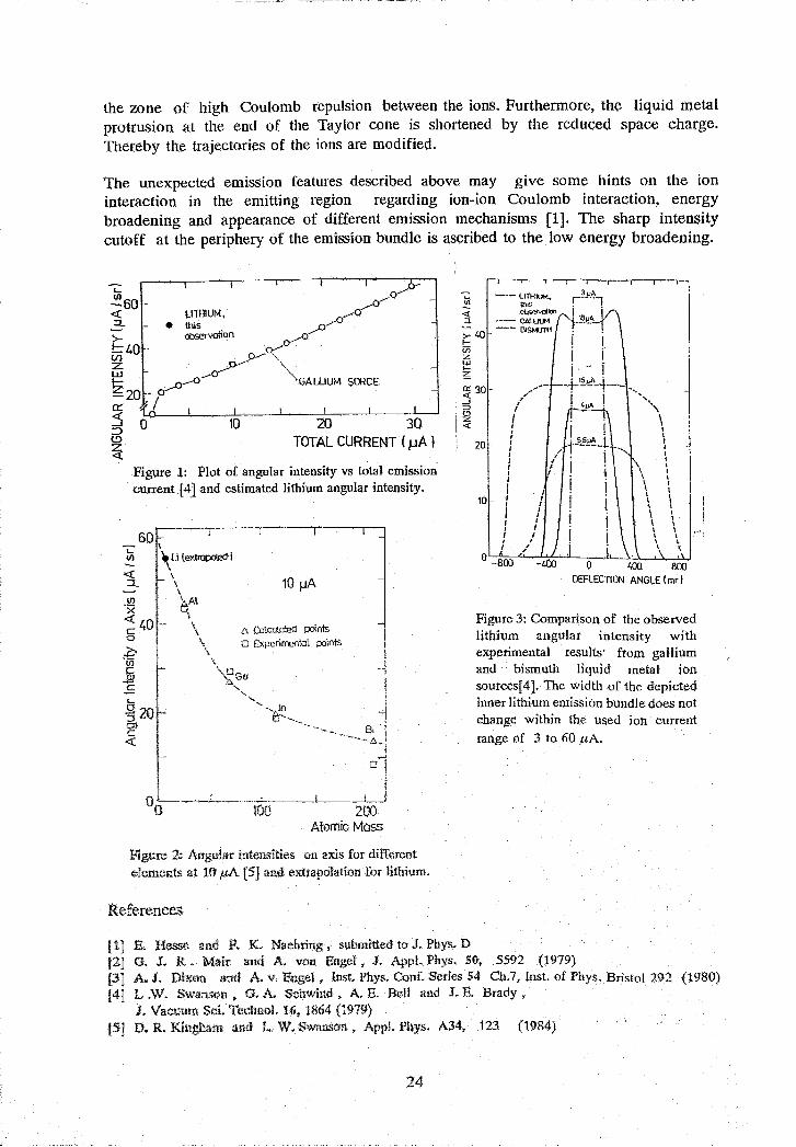
the Zone of high Coulomb repulsion between the ions. Furthermore, the liquid metal protrusion at the end of the Taylor cone is shortened by the reduced space charge. Thereby the trajectories of the ions are modified.
The unexpected emission features described above may give some hints on the ion interaction in the emitting region regarding ion-ion Coulomb interaction, energy broadening and appearance of different emission mechanisms [I]. The sharp intensity cutoff at the periphery of the emission bundle is ascribed to the low energy broadening.
TOTAL CURRENT ( pA 1
Figure 1: Plot of angular intensity vs total emission current [4] and estimated lithium angular intensity.
Figure 3: Comparison of the observed lithium angular intensity with experimental results from gallium and bismuth liquid metal ion sources[4]. The width of the depicted inner lithium emissibn bundle does not change within the used ion current range of 3 to 60 /LA.

Investigation of the Electrochemical Etch Stop on Silicon using KOH
B. Schmidt
The electrochemical etch stop technique is an attractive method for fabricating micromechanical struetures in silicon because it has the potential for allowing one to fabricate silicon microstructures and membranes with the thickness control on the order of rtO. 1 pm and with low doping concentrations fll The electrochemical etch stop of (100)-silicon in KOWH,O-solution arises in such a way, that there is an open-circuit-potential (OCP) of about -1.4 V against a reference electrode (RE). For applied cathodic and somewhat anodic potentials against OCP silicon etches but there is a passivation potential (PP) in the range -( 1.0 ... 0.8) V above which a passivating oxid grows (ariodization) and the etch rate decreases rapidly. The optimization of the etch conditions will involve the determination of the PP for n- and p-type silicon in the 30% KOWH,O -solution at T = 80 T. Furthermore , from the knowledge of the PP we can optimize the etch conditions for a reverse biased pn- junction to get ultra-thin monocrystalline silicon membranes of well defined thickness and with high accuracy. All electrochemical measurements were carried out using a EG&G PARC Model 362 Scanning Potentiostat. The etching was performed in darkness with the etch solution in a thermostat at T = (80&1) "C. The schematic three-electrode electrochemical etch configuration is shown in Fig. 1. Double-polished 3" p- and n-type wafers of (335A15) pm thickness and (1 ... 10) Qcm resistivity have been used to get the I-U-scans and to determine the OCP- and PP-potentials. The etch mask we used was'1.3 Pm thermally grown and patterned wet oxid. The wafers were mounted in a stainless steel holder, which protects the front side of the wafer from the solution. Furthermore , the Ag/AgCI- RE was immersed in a saturated KC1-solution and galvanically connected with ihe etch bath by a current key. Therefore we can exclude some interaction of the RE with the hot etch solution. During the I-U-scans the potential applied to the silicon wafer was scanned from -1.6 up to 0.0 V with scanrates of (2 ... 5) mV/s (Eig. 2 and Fig-3). From these measurements we have been determined .the following electrochernical potentials versus RE (Tabie 1):
11 Substrate I OCP in mV 1 PP in mV Table 1:
Electrochemical ppotentia1.r iFsr KOR at T=80QC
These values are &dar to that of 12,33 but must be always detennined for thie ghen etch conditions. The EU-curves for n- and p-type silicon wpecidly the cwents fiswing for cathodic potenitiafs differ vesy much. p-Si showes the characteristic backward biased diode for negative potentids (U ( OCP), whereas a-Si exhibits a luge "1 similar to a fomard b i s & diode. It is important, that in &I csisu;s at cathorfic potential relatively to the PI? sijicm will be etcbd md for anodic potentids gat8r PP the anodization and hereforf: &: etch stop d l l bv taka place,

From this etch behaviour we conclude the applied etch potential versus RE used in experiments for the electrochemical pn-junction etch stop during fabrication of ultra thin monocrystalline Si-membranes.
References [ I ] H Kloek, S.D Collins, N deRooij, and K.1,. Smith, IEEE Trans. Electron D a ices, ED-36, 663
(1989) 123 H. Seidel, Proc. 3rd Toyota Conference. Integrated Micro Motion Systems, Aichi, Japan, Oct.
1989. F. Harashima (Ed.), Elsevier Scxence Publishers B.V., 1990, p. 5 1 [3] SS . Wang, V.M. McNeil. K.-Y Ng. and M.A Schmidt, General Motors Research Puhlication,
üMR-6982, (1990)
-.
Fig. 1: Schematic three elüctrode electrochemical etch oontigurarion
Fig. 3: Voltam~nograrn of n-type siiicon
2

Electrochemical Etch Stop Behaviour on Ion Implanted Silicon pn-Junctions
B. Schmidt
In silicon micromachining the electrochemical etch stop have been often used on pn- junctions, which are usually formed on epitaxial n-type Iayers with thicknesses ) 1 Pm on p-type (100)-substrates. To obtain ultra thin membranes of precisely controlied thickness smaller than 1 pm n-type layers can be formed by ion implantation of phosphorous or arsenic ions and subsequent annealing and drive-in diffusion . The aim of the work is to investigate the electrochemical etch stop behaviour in dependence on the implantation energy, the implanted dose and on the annealing and drive-in diffusion conditions. TF,e experiments have been done with the three-electrode potentiostatic configuration as described in [11 To form thin n-type layers P+- and As+- ions in the energy range E = (30 ... 600) keV and with doses in the r a g e of D = (1~10'~.. .1~10~~) cme2 have been implanted and annealed (diffused in) at T = (800 ... 1100) OC for 30 min up to 12 h to get a wide range of the pn-junction depth (from 0.1 up to 10 pm). The investigations were carried out on 3" (100)-oriented p-type wafers with resistivities of p = U... 10) Qcm. Thermally grown and pattemed oxide was used as an etching mask. All samples have been etched in 30% KOH/H,O-solution at T = 80 'C . The etch rate at these conditions in (100)-direction was &„, = (6W2) pnh, which means an etch time of about 5 h. After a 3 5 h pre-etch the potential of U„ = - (902s ) mV relaevely to the AglAgCI-reference-electmde was applied to the implanted n-type layer and the current versus time characteristics have been measured by the I(t)-recorder.
p - substrate

Fig. 1 gives typical I@)-characteristics of ten etch samples during the last 20 minutes before the complete etch stop. The I@)-curves show that the current increases up to (1 l.5-tO.8) mA, corresponding to a current density of (1.8=tO. 1) m~lcrn ' and after at =
7.5 min the complete etch stop will be reached. The remaining current I„„ = (1.5rt0.3) mA corresponds to the anodization (oxydation) current of the samples. The experiments show that &er the complete etch ctop the sampIe may be stay in the etch bath more than 5 min without destmction even for the most shallow pn-junctions formed by 30 keV phosphorous implantation and 30 rnin annealing at T = 800 OC. Fig. 2 shows the observed difference of the I(t)-etch characteristics between ultra shallow junctions (implantation energies 5 60 keV and short annealing t .s; 90 min at 1100 "C) and deep diffused junctions ( tdiff 2 5 h at 1100 OC). For shallow junctions the initial current is smaller and and a sharper peak during the etch stop process can be observed. The twomaximain the curve are not yet understood. The remained membrane thicknesses after etching will be measured using the a - particle absorption (energy loss ) technique and additionally for membranes below 5 Pm using the Rutherford backscatterhg technique. From these metsurements we can investigate the difference between the thickness, where the etch stop takes place and the metallurgical pn-junction. There are some remarks in the literature [2] that the electrochernical etch stop appears somewhat before reaching the pn-jwction, but up to now there are no detailed and quantitative investigations of this effect.

A Measurement System for Studying Eiectrochernical Field Effect Ion Sensitivity
M. T. Pham, W. Taubert, and M. Bürger
CV measurements (capacitance voltage) on EIS stnictures (electrolyte insulator semiconductor) are the basic means for determining the electrical and electrochemical properties of ion sensing membranes used in ISFET microsensors. Cornmercially available instruments are highly specialized and are rneant either for the charaeterization of solid- state materials and devices or for purely electrochemical research works. An »in-betweem way that Covers both aspects is lacking so far.
Fig, 1: Circuit for dynamic capacitance measurement on EIS stnictures; CE: countsfr el~t tode, R E ieferenm electrode, W: working electrode, RV ramp voltage, SG: sim generatar, PS: potentiostat, BP: high p s filter, VCM: vector components meter, EB: feedback
The system we are using in Rossendorf for studying electrmhemi~a field effeccr ion sensitivity represents a synthesis of these iws techniques. Tha measudmg seheme is basal on the potential-controlled configuration deigned ilor thxs-electrode cell mmgernr:nt8 Pig. 1, with the working eiectmde (WB) belng the sampk under inves'tigaBwi. The key component of tho system is the dynamic capacitan~e mesmemenr usi detection principle, A small amplitude sinusoidal potential mrsdularion voltage via the &der-type potetftlostat, The eapacitim ca5pent phase

to the applied ac potential is measured by the vector components meter. For determining the flat-band voltage shift the system operates in the constant capacitance mode via an analog feedback unit. Fig. 2 shows the block diagram of the measuring system. All thle analog components are interfaced to a PC. The software used is LABWINDOW. The system is capable to perform 5 basic measuring techniques which are available in onie experiment series without need of rearranging the sample under test:
1) Quasi-static CV measurement 2) Small signal CV measutement 3) Measurement of the flat-band voltage shift 4) Determination of the polarizaltion 5) Differential measurement of two capacitances.

An Approach to the Cross Sensitivity of the Ion Sensing Membranes
M. T. Pham and S. Howitz
The common practice to take account for the Cross sensitivity is to »fit«, usually denoted as conditioning, the sample to the Sensor characteristics. This fails in continuous measurements. We will report here on the simultaneous measurement of the analyte and its interfering components using ion implanted membranes of mixed ion sensitivity. Differential measurements with ISFETs of different sensitivities are used as the basic concept. For determining two Parameters - pNa and pH - a three-membrane system is considered as a model:
Si,N, : sensitive to pH NAS 1 : sensitive to pH and pNa NAS2 : sensitive to pH and pNa
(NAS: sodium alurninosilicate)
With this system two independent differential output sig-nals (mV) are available relating to changes in pNa and pH as follows:
A, = (a fIapNa) ApNa + (a f lap~) APH for NAS,-Si&
A~ = (aglap~a) ApNa + (aglap~) APH for NAS2-Si,N,
The four partial differential coefficients are the ion Sen- sitivities s„, S12, S„, Szz of the corresponding differential ISFET pairs which wem determined experimentally in solutions with constant pNa (or pH). The indexes l ;an$ 2 refer to the two NAS membranes respectivdy, The changes in pNa rind pH are deduced from A, and A2 which represent the quantities to be rncsasured in the actud si-tuation:

Vo/mV 40Q,
i -
{ NAS Si3N4
Fig. 1: Exampie of the sensing funciion of the integralted Sensor with three-membrane System: Si&- NAS1-NAS2. Measured output signal of the differential pair Si,&-lNAS1-ISFET in dependence on the pH-in electrolyte with 0.1 molll NaCI. NAS rnembranes were prepared by implanting Na+ (42 keV) and Al+ (60 keV) into the Si0,layer of the ISFET gate to a total dose of 2 x 10¹⁶ ions/cm2. The thennal . treatment was conducted at 700 'C in N, for 20 min. An etch step in buffered HF was followed to reveal the buried membrane.
1 2 3
Wa
Fip. L.: Deterhnarian of pNa (denoM by m) from S md A showing the dependence of linnlt sn plH
the detection

ISFETs with Controlled Gate Membrane Opening
M. T. Pham and S. Howitz
ISFETs with an acceptable lifetime are needed in continous measurements in closed flow systems which do not permit any interruption during the system operation. Currently available ISFET microsensors suffer from the fact that they are either short-lived or the lifetime is indefinable.
We present here the concept mdundancy Sensor« based on ISFETs with buried gate membrane. The mew structure enables the ISFET to appear in two defined states: active and passive. In the passive state the buried membrane has no direct contact to the electrolyte, thus it is protected f i ~ m any electrolyte attack being one serious cause for deteeürating the lifetime. In the aictive state the membrane is exposed to the electrolyte. Using such ISFETs in an anay a desired lifetime of the system may be achieved by controlled opening of the gate membrane.
The common stmcture of an ISFET is the one with Open gate window required for exposing the membrane to the test solution. We design here a new structure having buried gate membrane md study the technique for the insitu opening of the gate window in the measuring solution. The buried structure used in this experiment is a SiO, membrane covered by a metal layer having 'parameters similar to those of the ISFET gate: metaUCVD-Si0,/Si3N41Si021p-Si (with 100 nm CVD-Si02, 100 nm Si3N4, 70 nm SiO,). Exposed to the electrolyte solution the membrane has no contact to the medium and remains thus in the passive state as Song as the metal coating is still present. Only after removing the meta1 coating the membrane can develop its ion sensing function by directly contacting the solution. The anodic dissolution of the coating metal was studied for opening the gate membrane using a cylinder cathode of Pt. The anode area exposed to the solution was defined by an epoxy encapsulation. The electrolytes were solutions of defind pE (2, 7 and 10) cantaining 0.1 mol/l NaCl. The dissolution process was followed microscopically. For Al (thickness of 100, 600 and 1000 nm) as ~oating metai the following results were obtained:
a) A favorable working regime was found to be 1.2 - 1.4 V for the anodc-cathode vohge with a current d~ensity of 5 - 8 Aldm2. b) A more clean removal of AI was aehievd with solutions at p H 2 and 10 compared to that at pH 7, C) The dissolution is accompanied by an intensive gas development which favors the dissoiution by intensifyhg the mass transport in tlne solution. d) The dissolution process was seen to be faterdily inhomogenenous resulting in a proper removal in the edge regians rljacmt ito the egoxy encapsulation while leaving behind isolated islands unetchd in the centre. Although a quantitative removal of Al is thus not achievable in the present configuration thert: 'dfe m detrimentaS consequences to be expwted with respect to the ion seming fu~ction db the potentiometric measurement does not depend on the surf-ice gmrnells; Fig. 1 gives

example o f a buried oxide membrane after the window opening.
Fig. 1: Mictoscopic picture of a buried Si02 membrane after removing the coating layer Al, 1000 nm indicating the encapsulation boundary @lack vertical line, ieft), the unetched rernainder of Al (isolated islands visibleas bright spots scattering from the middie to the nght edge) and the membrane region (remainiig dark background)

Ion Beam Modified Insulator Layers as ISF'ET Membranes for Heavy Metal Ion Detection
J. Hüller, W. Hoffmann*, and M. T. Pham *KfK Karlsruhe
Our work of the ion beam modification of membranes for ISFET has been extended to modification of heavy meta1 ion sensitive membranes last year. Basic material and orientation for the kind of modification is a group of new solid-state inorganic materials: chalcogenide glasses [I]. They have been successfully used as ion sensitive membranes for determination of Ag+, Cu2+, Pb2+, Cd2+, Hg2+, Fe3+ and Tl+ concentrations in liquid media [2], [3]. We have realized three different types of preparations of the Si/SiQ/Si,N4/Si0, layer structure. In the first case the upper CVD-Si@-layer was etched way and replaced by a 300nm thick AgS%- or As2S, layer, respectively, deposited by r.f. sputtering done at the St.Petersburg University Chernical Sensors Laboratory. These layers were undoped or homogeneously doped with 10 at% Cu or Ag, respectively . In the second case the undoped AgSe, was ion implanted with Cu in the dose range from lx1015 cm-2 to 1x10¹⁶ ~ r n - ~ . In the third case - in sequence the first - the upper S iQ layer was implanted with different doses of Cu andlor Se at 30 keV energy in the dme region from 1014 to 4x10¹⁶ ~ m - ~ .
These experiments were destinated to clear up the principal phenomena concerning the measurability of such electrolyte insulator semiconductor (EIS) Iayers. We have investigated: shape of the quasistatic arid small signal C(U)-curve; position of the flatband voltage U, within the measuring range of the ATIR capacitance measuring device of +/-W; wettability of the surface; chemical etching behaviour; influence of the ionic strength of the measuring liquid; influence of the type of the reference electrode (Pt or calomel). Fig. 1 shows the Cu-sensitivity curve of a sputtered A$S%- layer .
This type of graph is typicdly for CONCAP membrane sensitivity meatsurements at constant capacity near U,. Besides of the Cu-sensitivity effects as drift, response, hysteresis and reproducibility may be studied with this methd, The spsg~tterd chalcogenide glass layers have a poor adhesion and homogeneity, This may be the reason for a remakable pH-cross-sensitivity , caused by the undetlaying Si3N44ayer. The aim of our future work will be the synthesis of doped bulled As2Se, layers by direct implantation of As, Se and Cu in SiO„ In correlation $0 eIwtrochemicaJ, properties as sensitivity and selectivity it is necessary to optirnliie the implantation an& annealing conditions.

parameter: pCu
Zeit [ s ]
Fig. 1: Cu-sensitivity of a sputtered A@e, layer, homogeneously doped with 10% Cu
References 111 Yu. G. Vlasov, E. A. Bychkov and A. M. Medvedev, Analytica Chimica Acta 185, 137 (1986) [2] Yu. G. Vlaaov, Fresenius Z. Anal. Chem, 33592 (1989) [3] Yu. A. Tarantov, Yu. G. Vlasov, A. Mesentsev and Y.L.Avexyanov
Sensors and Actuators, BI, 390 (1990)

Differential Measurements with ISFETs in Microfluid Systems
M. T. Pham and S. Howitz
The microfluid system represents the »backbone« caf the Fluidic ISFET Microsystem (FIM) for chemical analysis which we are currently developing in a project financially supported by the Sächsische Staatsministerium für Wirtschaft und Arbeit [I]. It comprises an array of microsensors linked up to a system of microcapillaries and both components are an integrated unit assembled on a Si wafer. The measurements are conducted for a) gaining a first insight into the constructive details for technology optimization and designing works, b) learning to control fluid movements towards destined sensor elements embedded in the microcapillaries, C) studying the signal development and acquisition under dynamic m ~ ~ u r e m e n t conditions.
Fig. 1 gives the schematic cross section of the microfluid system. Using the KOH-Si
.. .. ., . . - glass cover ,.--, spocer Ei substrake
Fig. 1 glaa*,
: Cross sectional view of the microfluid system prepwed by KOH-Si etching, ele(:trochemkal drilling, silicon anadic bonding and epoxy gluing
etching a meander microtrench of a total length of 2.4 m arid a cross section of 200 x 500 pm2 was etched into a Si wafer and covered by a, glass shet by modic; bonding to form the microcapillaries. The latter are provided wlth a series of via openings fOr sensor installation while several drill holes for fluid inlet and outlet are av.aiIab1e On the glass cover side. Microsensors used are ISFETs with Si& membmne. External pump and valves were used in this experiment. Tht; differential signal between tws TSFETs was measured in response to perfusing the fluid channel with Wo pH sol~tioris dternately- Tbc: reerod shown in Fig.2 is typical for the serial ISFBT arrangement demonatrating

Pig. 2: Differential Signal of two pH ISFETs serially arranged in the fluid channel in response to pH changes, arrows inaicating the moment of solution intet, the recording was obtained for a constant flow rate at room temperahite, solutions used were pH buffers at 2 and 9 containing 0.1 molll NaCl
the usefulness of the System. A number of problems have to be studied in more detail, and in particular we might note: - dependence of the response time on the direction of
concentration changing - hydrodynamic aspects in correlation with the capillary
construction for controlling the radial and axial fluid franfer rate
- corifamination of the medium due to the wall adhesion resulted from inereasing surface to volume ratio by scding down the fluid channel
- fluid mixing and the systern sensitivity determining the detecting resohtiorr
- response time and fitting Sensors into the fluid channel
Weferences [l] S. Wowitz and M. T. Pham, Fluidic ISFET Microsystem, this Report.

Cooperative Project l'Fluidic-ISFET-Microsys tem"
S. Howitz and M. T. Pham
If using Systems in sratic measurement, there are generally still a number of serious problems arising from ISFET inherent characteristics,and in particular we might note: signal drift, Cross sensitivity, restrictive lifetime and micro reference electrode. The concept of creating a dynamic measurement system which enables chemical analysis to be done reliably by using ISFETs with currently available properties is the new motivation for research and development of ISFET based micro sensors. The FLUIDIC-ISFET-MICROSYSTEM (FIM)[l] represents one alternative way to employ ISFETs in a dynarnic measurement mode useful for the multiion analysis.
The new approach followed by the ISFET research team in Rossendorf is to link up -present-day results from ISFETs with present-day results on the field of micro system technique for example micro mechanics, micro elctronic measurements, micro packagings and Sensor research. The dynamic measurement system will make possible the defined sampling of the analyte in the pl-nl range, the real- time calibration, the differential measurement with ISFETs of identical properties, and the intelligent data evaluation. The cmx of this idea is the utilization of ISFETs of the current technical level for the exact multiion analysis. The applicative flexibility of the FIM will be reached by a fully modular and hybrid micro packaging. A system of micro packaging and micro interconnection technologies will perrnit the intelligent combination of sensors, actuators, and logic elements. The aim of that cooperative project currently in Progress is the simultaneous detection of pH, pNa, pK, and pNO,. Participants of the project started in Nov. 92 are Centre-Microelectronic-Dresden, Fraunhofer Institute of Microelectronic Circuits and Systems Dresden, Institute Fresenius Dresden, and Research Centre Rossendorf, In Fig-1 are shown all elements of the FIM-microsystem schematically .
PUMP -
FLUIDIC- . .
CAPILLARY
ISFET-ARRAY . ACTIVE .4ND REDUNDWCY
HYBRID-IC& - - ASIC -LOGIC

The innovative scientific intentions of project FIM: I.Back-Side-Membrane ISFET; examination of the following alternative SOI- technologies, a) Separation by Implanted Oxygen SIMOX; b) Separation by Implanted Nitrogen and Oxygen SIMNOX; C) p-n junction etch-stop and LPCVD-Si3N4 of the sensitive membrane area
- - --. - DRAIN-SOURCE-METALL
BURIED INSULATOR Si,O-SiO&-Si3N4 BACK-SIDE-ISFET
MEMBRANE
Si-GLASS FLUiDIC CAPILLARY SYSTEM -
Fig.2: Cross section of a Back-Side-Membrane ISFET in SIMNOX using the N+-0+-implantation in silicon
iI. Redundancv-ISFET[2]; based on the idea to passivate a conventional solid-state membrane of ISFET using Cr-, Cr-Ni- or Al- thin films which can be removed away, if required, by an electrochemicd dissolution process (Fig.3).
4 b) Fig.3: Back-Side-Reditndancy ISFET; a] before and b) after the
electrically stimulated activation-
IIl,The micromachined fluidic svstem is made by Silicon-glass technology and cornprises piezoelectric actuated planar valves (Wo-way valves from Joswig are used [3]"jd forced fiow ISFET Sensors embedded in a fluidic capillary system as integrated compsnents, The assembly will be qualified by the help of FEM modelling and simttlation calculations.
FWIDIC INLETs REDUMDANCY ISFET ARRAY

FLUIDIC SILICON-GLASS FORCED FLOW ISFETS IN CAPILLARY SYSTEM SPACERCHIP TECHNIQUE
I '_
PLANAR PIEZO VALVE
Fig.5: Cross section through the fluidic capillary with piezoelectric actuated valve, active ISFET, and Redundancy ISFET
IV. The svstem of intelligent data evaluation:In the first stage a suitable macro measuring system as shown in Fig.6 is developed, the macro system wiii be able to evaluate measuring signals delivered by a matrix of ISFETs with Cross sensitivity. The effective procedures of calibration and evaluation are to be found here. The second stage consists in an optimization arid miniaturization process where necessary components for specific ASICs are to be developed.

Depth Profiles of C, N and 0 on Carbon Coated Steel
Surfaces Made by IBAD
A. Kolitsch, E. Hentschel, and E. Richter
The infiuence of simultaneous deposition of carbon layers during ion implantatisn of nitrogen ions to the wear and friction behaviour of tool steel surfaces was investigated . An ion implanter without mass separator and a vacuum system with oil difision Pumps was used. Such a vacuum system is a potential source of target contamination by hydrocarbon cracking products especially in connection with long implantation times. It is to investigate the infiuence of this carbon layer in means of wear and friction data and the characteristics of this layer system by elastic recoil detection analysis (ERDA). In comparison to the ERDA results also AES depth profile masurement was used.
Samples of ZlOCr46 tool steel were implanted with 8x10¹⁷ nitrogen ionslcm2 of SOkeV energy and a low bearn density of 4 p ~ k m 2 at different vacuum conditions and different
oxygen admixture of the ion source gas inlet (Table I).
Table 1: Sample preparation
sample baffle gas inlet for ion source no, temperature I 25OC 100% N2 2 400c r 00% NZ 3 25OC 80% N2/ 20% air 4 40°C 80% N2/ 20% air 5 25OC 60% N21 40% air
40°C 60% IN2/ 40% air
A conventional EKB geometry has been applied at the Rossendorf Tandem accelerator. The primary beam of 35 MeV 3 5 ~ 1 ions was directed onto the target and a Bragg-
chamber (BK) was mounted at an angle of 30° with respect to the beam axis. atisn of the target surface was chosen to keep a glancing angle of 150 for the nd oeitgoing psirticles. Th quantitative treatment of extracting depth profiles
ne at a V/& statiun 3 1 0 M76. The calculation of the stopping power is de of Ziegler et al. [I J and on the Bragg rule for a composed system. elastic processes with the Rutherford cross section the spectra of the
$4 and C isns as well as of the scattered primary C1 ions are calculated. er is simuiated in 300 slabs by trial profiles of Fe, 0, N and C. The trial
al prmedure by comparing the calculated and measured ions are necessary to produce a perfect fit of all the
rnatbn of the projede spectmm, A physicaHy re- a Wiener-KoimagoroE-filter.
aPHy aBer iqlantatian in the sarnples No. 3 and 4 with a saurce EoIiiowed by sa es No. 1 and 2 without ion with a &her oxy content of the nitrogen

ion beam decreases the wear resistance (samples No. 5 and 6) up to the values of non implanted steel (No. 0). On the other hand, it is to recognise that in all cases the implantation with 400C tempered baffles of the oil diffusion pumps produces a better wear resistant layer than with 250C tempered baffles. The wear resistance as a function of optimised carbon coating process means to optimise the deposition rate as a function of the baflle temperature and means to optimise the carbon layer thickness as a function of the duration in the implantation chamber. Fig.2 illustrates the attached energy spectrum of the 3 5 ~ 1 projectiles and the recoiled Fe, C, N, and 0 atoms. The calculated depth profiles of Fe, C, N, and 0 are to See in Fig. 3. The range order of these elements in the surface region is well defined. The Start of the iron profile is not exactly at the surface. To be observed is a wide oxygen profile immediately on the iron surface and with a range into the iron surface. It is evident that the original steel surface is coated by an iron oxide film caused by the stay in air. On this oxygen profile was analysed a carbon layer irnmediately at the steel surface, And the analysed nitrogen profile has a range order through the carbon, oxygen, and iron surface profiles. The nitrogen profile resulting from the implantation process with 50 keV Nf ions has not only caused the composition of chemical compounds in the steel matrix but also an ion beam induced mixing process is effected in the surface region. This mixing effect at the interfaces and the ion beam assisted deposition of the carbon layer are creating the good wear resistance by high adhesion of the carbon layer and formation of chemical compounds. The flat geometry of the nitrogen profile refers to the dynamical growth of the carbon layer on the surface at the long implantation time. The samples 1...6 show nearly the same depth profiles. The resulting range order of the depth profiles is not changed. The different wear resistance cannot be explained by depth profiling. The most thick carbon layer with greatest peak height has been measured afier implantation with an ion beam without oxygen particles, but this sample doesn't show the best wear resistance. The sample with the best wear resistance is the smallest carbon layer of sample No. 4 with a medium air inlet into the ion source. An increasing of the hydrocarbon cracking products in the vacuum chamber causers a thicker carbsn layer. The comparable irrvestigations of this layer system by AES depth profnling have the Same result s.
The results have shown that elaseic recoil detection analysis is a very good instmmen depth profiling of thin layers of light elements in metals. The rne~hod ailows the an of profiles down to concen 1% ~f the stoiclxi mrjtric snes ri~nd the depth resolution up to 5 or The investigated problem of ion beam assisted depositisn of carbon Bayers to the nitrogen ion implanltation into steel caused by coating of hydfoc products of 03 diffirsion pumps could be explained in direction to tbe Iqers stmctu~, the range ordcr of the surface 1-ers, snd the eiement distgbuti~n in the new $U region- For the mgtriination of the wear resistance behsiviou additionriily the phase statq lattice, parmeters, and claerni carbon i q e r in direction sf dianiowd IPke carb

Fig. I: VoIume abrasion vs sliding distance for nonimplanted (No. 0) and implanted (No. 1 . . . 6 ) 2 I OCr46
10 J
n 4
Q,
10" 9 0 2 lo= 4 F1 0 0 10 U
1 0 50 100 L50 200 250
energy [channels]
tool skel
Fig. 2; Energy spectra mmured at sample 2 fiorri aiomic charge number 6 (C), 7 $7, ö (W, 26Ve) aid 17(Cij
Fig. 3 r ogen and irsn measured by ERDA in 210Cr415 tool steel &er- i ~ i t i
iorn~cm2, d e t ~ c m 2 , 6010 minutes stay in the vacuum cfiarnber, ing water* gas idet into ion source: B 00% purest r\f7
5

High Dose Implantation of Aluminium into Iron
H. Reuther, 0. ~ikolov''*, S. ~niijer", ~ . ~ . ~ r a n d + + , W. ~eune"
"~niversität Duisburg, Laboratorium für Angewandte Physik, Lotharstr. 1-21,
W-4100 Duisburg, Germany * Permanent address: Institute of Nuclear Research, 72 boul. Tsarigradsko Shosse,
BG-1784 Sofia, Bulgaria
Iron-aluminium alloys are of some interest both for fundamental research and for
technology. Especially the iron-rich alloys show interesting magnetic properties
bekause there is a transition from ferromagnetic Fe3AL to non-magnemc F ~ A I at 33
at% Al [I]. In surface layers they can be produced by ion beam techniques
especially by ion beam mixing [2-41 or by direct ion implantation [SI. In this paper
the dose limit for the formation 05 the non-magnetic phases was detemined.
Moreover, depth selective CEMS (DCEMS) was applied to investigate which
compounds or stmctures are fomed at different depth.--
Iron samples (1 mm thick, 99.99 % Fe) were implanted with doses between 1x16 17
and 5x10'~ Cme2 (50 and 100 keV energy) and 1x10'~ cme2 (200 keV). For the
DCEMS investigations a 7 pm thick a-iron foil enriched to 95.10 % 5 7 ~ e w a ~ used
and implanted'with 5x10'~ at 50 keV. n i e CEMS measurements were
performed at room temperature. The Same conditions as described earlier [GI were
used, A description of the DCEMS System will be published later.
In Fig. 1 the CEM spectra and the calculated hyperfine field distributlons of the
aluminium implanted iron samples are shown for an elxxgy of 100 keV. B is seen
that a dose of 4x10'~ is necessary to produce non-magnetic components
(singlet line). At an energy of 50 keV a dose of 5x10'~ cmh2 was neccssary while
at 200 keV even with 1x10 cme2 &her than ferromagneti~ fractions appeared (a quadrupofe doublet). At lower d ~ s e s only hyperfine Geld distributions with
ferjromagnetic components were fouxld, Moreover, aU spectra crrntah the characteristic six-line-pattern of a-iron.
These recults showed that not 0nf.y thc conc;e~tration but als0 the dep

Fig. I: CEM spectra and calculated hyperfine field distributions of Fe implanted with Al
The results of the DCEMS measurements are shown in Fig. 2. The spectra are
pfot-ted for various electron energies from top to bottom in the order of increasing
probing depths. While for 6900, 6600, and for 13400 eV the spectrum consists of a
main nonmagnetic cornponent with minor magnetic fractions in the case of 12750
and 10500 eV magnetic cornponents predominate. This means that the nonmagnetic
phase is formed only in and near the sampne surface,

Fig. 2:
1 1 1 1 1 1 1 1 1 1 I -8 -4 0 +4 +8
VELOCITY (rnm/s)
DCEM spectra and calcuIated hyperfine field distribotions of the AI implanted 5 7 ~ e foil
References
[I] H. Chacham, E. Galvao da Silva, D. Guenzburger, arid D.E. Ellis, Phys. Rev. B35,1602 (1957).
[2] V.P. Godbole, S.M. Chaudhari, S.V, Ghaisas., SM, Kanethar, S.B. Ogaie, and V,G,Bhide, Phys.
Rev. B31,5703 (1985).
[3] C- Jaouen, J.P. Eymery, E.L. Mathe, and J, Delafond, Mat. Sci. Eng. 69,483 (198.5).
141 M.A.Z. Vasconcellos, S R . '&eieixeira, F&, Freire, Sr., M.C.S. Nobrega, P.8- Dionkfo, W-H.
Schreiner, and 1J.R. Baumwi, Mal. Sci. Eng. A104,169 (1988).
[5] H. Reuther, Nucl. Instrurn, Methods B53, 167 (1991).
€61 R Reuther, Muci. Instrurn. Methodc B30,61 (1988).

A Magnetron Source for Ion Implantation
H. Reuther
In the past the implantation of metal ions in sufficient doses (5x10'~ cmM2 and
more) caused difficulties because of the lack of suitable ion sources. It was
necessary to use light volatile or vaporabk compounds of the metal and to separate
the ion beam with the disadvantage of decrease of beam intensity [I]. Due to the development of sputter and vacuum arc sources (CHORDIS [2,3] and
MEVVA [4]) these disadvantages have lbeen redressed. Here an additional sputter
source utilizing the magnetron sputter principle is presented.
The ion source was constructed on base of the well known magnetron pnnciple used
for sputter deposition 151. A target is situated on a permanent magnet which
generates the required magnetic gap field. The configuration of the magnetic field
and the eiectrode array creates a ring shaped plasma of high density on the target
surface. The discharge current contains both electrons, ions of the carrier gas and
ions of the target. Moreover, a large amount of neutral particles is sputtered from the
target.
The idea of the present work was to utilize the ionic fraction of the magnetron
discharge current for an ion source. At bias sputtering at less than 500 V the ion
current can already amount to up to 8 % of the total current [6]. The ion fraction is
composed by ions of both the carrier gas and the target.
Using a magnetron discharge for an ion source two main problems have to be
solved. The first is to overcome the differente between the pressure necessary Eor
operating the magnetron (>0.1 Pa) and the pressure normally used for ion
implantation (dr3 Pa). The second is to minimize the carrier gas fraction in the
ion current. Both problems have been solved by the constniction of the source and
optimization of the working parameters.
Elg. 1 shows a section OE the magnetron source. Heart of the source is the magnetron
ctrmposed by fhe taiget (I), the rod magnet (2), the ring magnet (3), and the pole
piece (4) producing the circular magnetic fieid, the inner (5) and the outer shielding
(G), and the insufator in between (14). The target is water cooled (8). The argon
carriet- gas 1s filled in by the gas inlet (13). The magnetron discharge is started by
putting a voltage of some 100 V betwem target and outer shielding. This is the
rromal magnetron opielation &ich coutd be used for deposition processes.
The idea was to include tfie magnetron discharge in a chamber with a smail aperture
.fef the ion extt-ction flux. 'rhereforc the outer shieiding was lengthened and cIosed

with a lid (9). This lid has a circular aperture and serves as ion extraction screen.
The lid is water cooled. In front of the extraction plate an also water cooled plate for
suppressing secondary electrons (10) is situated. Behind it the screen at implanter
terminal potential is mounted (11).
The source holder together with the
power and water cooling connections is
mounted on a flange. Between this and
the implanter terminal beam line the
high voltage insulator (15) is situated.
The source is screened from the other
components of the implanter terminal
beam line by a cylindrical tube (7).
The inclusion of the magnetron in a pot
with an only small aperture has the
advantage that the pressure in the
source can be much higher than in the
recipient. It is necessary both for the
magnetron operation and the ion
implantation process.
Fig. 1: Section of fhe magnetron ion source
The source was tested with Mo, Al, Cu, Ti, and Ta sheets as source targets, The
fraction of metal ions in the ion beam was detennineci at different carrier gas
pressures. Argon was the carrier gas in every case. The highest metal ion fractions
were surprisingly detected at the highest carrier gas pressure. The integral currents
were in the range OE some mA, the maximum metal ion fraction was behveen 47 %
for Ti and 83 % for Cu. [7]
References
[I] N. Sakudo, Nucl. Instrum. MetIiods B21,168 (1987).
[2] R, Keller, P, Spädtke, and H. Eniig, Vacuu~n 36,533 (1956).
[3] B. Toip, B.R. Mielsen, D.M, Rück, H. Emig, P, Spädfke, and B,H. Wolf Rw. Sei. In~trxm. 61,

Modelling of Implantation-Induced Transient Diffusion and Electrical Activation of Boron in Crystalline Silicon during Post-Implantation Annealing
H. U. Jäger
The formation of shallow p-type regions in crystalline silicon by low-energy boron ion implantation and subsequent thermal annealing is characterized by some specifics (see refs. [1,2], and the refs. cited therein). Fig. 1 shows typical experimental data from the
literature as wd l as results -. . - 1 from our simulations. For
such a low-temperature furna- ce annealing at 800°C the normal diffusion is known to be negligible, However, in case of post-implantation an- nealing the as-implanted boron profiles become modified in their tail regions up to a criti- cal concentration C„ of about 4x10¹⁸ ~ r n - ~ , which is of the same order of magnitude as the intrinsic carrier concentra- tion ni at this temperature, but far below the corresponding boron solid solubility limit C„, = 3 . 2 ~ 1 0 ' ~ cm". This implantation-induced tail diffusion relaxes within a time period of about 30 min. The non-diffusing, static boron peak region above C„, is found to be electrically in- active (Fig. lc). It becomes electrically active only after annealing periods of many hours.
Fig. 1: Time evolution of a) boron atomic profiles, b) point defect dis- tributions and C) electrical profiIes in silicon during 800°C furnace anneaIing after 25keV 2~10'~crn-~ B ion implantation. The simulations are compared with boron profiies which have been measured by Cowern et al, {2] using secondary ion mass spectroscopy (SIMS) and spreading-resistance profiling(SRP).

We have modelled this boron diffusion and activation by a system of coupled diffusion- reaction equations 131. For the diffusion terms in the equations, the concept of point de- fect impurity pair diffusion [4] has been adopted. A dopant concentration C,,„,., not excd ing the solid solubility limit C„ is assumed to consist of ionized substitutional dopmt atoms A L (acceptors: q=-1) and of neutral dopant atoms A„ on interstitial sites. Besides vacancies V" and silicon self-interstitials I" in various charge states z are taken into account. The substitutional dopant atoms and the point defects form the pairs
which are postulated to be the only dopant-containing diffusing vehicles. In addition, there have been assumed (i) local equilibrium between the reaction partners in eqs. (1) and (2), (ii) local equilibrium for all reactions changing the charge states of the species, and (iii) pair concentrations which are dilute compared to the concentrations of isolated dopants and point defects.
We suggest that during annealing the interstitial outdiffusion to the surface or into the bulk leads to an increase of boron activation via the "kick-out" reaction
If this idea is accepted, it is forrnally straightforward to take into account also the inter- stitial-vacancy annihilation or generation
and the incorporation of boron on substitutional sites by vacancy annihilation (Frank- Turnbull mechanism)
These reactions have been ttiken into account under noneqiuilib5um conditions, Wir respective reaction rates in foseward and backward dirwtion are defin& h brnaulae

The present investigations are aimed at the modelling of implantationrinduced effects in boron diffusion and activation, but the details of defects evolution during ion implanta- tion and during heating up to the annealing temperature are beyond the scope of this study. Therefore the problem arises to find adequate initial defect distributions. Let us postulate that a very early stage of annealing exists, where diffusion is still unimportant, but Iocal equilibrium between the reactions (3) - (5) has been aiready achieved. The local equilibrium obtained can be characterized by the concentration difference Q = C, - C, - C , „ , which is not changed by the reactions (3) - (5). A depth region with originally qua1 numbers of interstitials and vacancies and only inactive boron atoms (cB,„=O) is characterized by Q=O and equilibrates, in this approximation, to the concentrations
The states in eq. (6) calculated for all individual depth intervals represent our initial dis- tributaon in solving the complete system of diffusion-reaction quations.
The calculations have been performed using the new module for point defect - based diffusion [5] in the one-dimensional process simulator TESIM [6]. All the diffusion parameters, incl. C; and C;, have been adapted from the work of Roms et al. [7]. The other kinetic parameters characterizing the reactions (3) - (5) have been obtained by fits to experimental data. As a consequence of aur model parameters both the interstitid- assisted boron diffusion (1) and the interstitial-assisted boron activation (3) are predicted to be dominant. Our assumption that interacitions between a substitutional boron atom B„, and an interslitial I may lead to two different reaction products (compare eqs. (1) and (3)) is new. 1t is considered to be a possible approach and has conceptually a simi- lar function as the dynamic clustering model in the investigations of Cowern et al. [8].
Acknowledgements This work was supported in part by the Bundesministerium für Forschung und Techno- logie under Grant Mo. 211-5291-03-HE3ROS. Thanks are also due to the Fraunhofer- Institut für h/IikroeIektronische Schaltungen und Systeme, Institutsteil Dresden for the possibility tu work in this institute as guest scientist.
References [I] S, SoImi, F. Baruffaldi, and R. Canten, J. Appl. Phys. 69 , 2135 (1991) 121 N. E. B. Cowern, K. T. F. Janssen, and H, F. F. Jos, J. Appl. Phys. 68 , 6191 (1990)
th Internatianal Canference on Ion Bwm Modification of Materials, Heidelberg, Gznnany, Sept. 7 - t l , 1992, eontr. paper P232; to bepublished in NucI. Instr. & Meth. Phys. Res. E3
[4l 13. J. MuPuaney and W. B. ltitrhatdson, AppL Php . Lett. 51 , 1439 (1987) &53 J. PGrrisch, Dipbma Thesis, Technische Unitrersifiit Chemnitz, Sektion Mathematik, 1990
Mikmelekt~onische Schaltungen und Systeme, Institutsteil U Orden, Oenaany Mozehmd, R. F. Lever, J. P. Peng, and 0. Re Srinivasan, IEEE
Trans, Camp.-AiW Design 8 , 1 X T 3 (19 F, Jas, K* T . P. bnsseni, and A, I, H. Wachters, M&. Res. Soc. Symp.

Computer Simulation of C hanneling Irnplant at ion of ~ h o s ~ h o r u s into Silicon
M. Posselt
In the last two years detailed experimental investigations on channeling implan- tation of phosphorus, boron and nitrogen at energies between 10 keV and 2 MeV have been performed (cf. [l-51 and references therein). Theoretical calculations of range distributions for channeling implantation of heavy ions are relatively dif- ficult since the shape of the range profiles is strongly influenced by the radiation damage produced during ion bombardment. Furthermore, the shape of the range distributions depends on the alignment and the divergence of the ion beam and on the thickness and the structure of the thin amorphous oxide layer on silicon. We developed ths binary collision code Crystal-TRIM to simulate ion implanta- tion into single-crystalline solids. This program has been elucidated in detail in refs. [3-51. The electronic stopping of the ions is described by a modified Oen- Robinson formula: The electronic energy loss is an exponential function of the impact parameter, It is normalized to the ZBL electronic stopping cross-section [6]. The motion of the projectile in the thin amorphous surface layer is simulated similarly to the TRIM program [6] using the mean atomic distance as the free flight path. The generation and accumulation of radiation defects during ion irradiation is taken into account approximately [3-$1. We assume that in the crystalline target Frenkel pairs are produced by ballistic processes. The recombination of vacancies and interstitials is neglected. The lattice positions of the interstitials during ion bombardment are not known exactly. In our algsrithm we regard the interstitials as randomly displaced from tetrahedral sites within a sphere. As the radius of the sphere we choose the mean atomic distance in the crystalline target. The ion dsse D, is simulated by N pseudoprojectiles. Each pseudoprsjectik csrrespsnds t s a dose increment dD = B,/N. In a depth interval '(z,x+AzZ') of the lasget tha

10l8 I'IIMNI i n ß i [IOO]
SIMS
Fig. 2: Range profiles for 1 MeV channel- ing implantation of P+ ints silicon at differ- ent doses. The experimental data were o b tained by Raineri et al. [1,2] using SIMS arid spreading resistance depth profiling (SRP). The theoretical profiles were calculated with- out (thin solid lines) and with (thick solid lines) the consideration of radiation-induced defect production. The thickness Af the amor- phous surface layer was assurned to be 50 A.
probability dpd tkat an atom is displaced by a pseudoprojectile is given I3y
w k r e n is the atomic density in the crystalline target. The quantity Nd clenotes the nurnbsr sf displacerneuts which woulci be created in (X, X + Ax) if the pseudo- proJceti8e NM be imdanted into a virgiri crystal. The reductiori of the riumbcr 01 atorn~ whish can be displaced Srsrn their si tes is taken into account by the fackx
54

(1 - pd). The probability pd is equal to the probability pv that a lattice site is occtz~ied by a vacancy. In general the depth profiles of vacancies are nearly equal to tlhe depth distributions of the interstitials apart from a small shift. Therefore, we aet the probability pr that in the depth interval (X, X + Ax) an interstitial site is occupied equal to pv. In (X, X + Ax) uniform distributions of vacancies and interstitials according to the probabilities pv and pr are assumed. For the first time the dose dependence of range profiles in high energy channeling implantation was simulated by a binary collision code. Range distributions calcu- lated by Crystal-TRIM are shown in Figs. 1 and 2. The range profiles obtained from channeling implantation experiments of Raineri et al. [1,2] are also given. Fig. 1 shlows theoretical range profiles calculated without and with the consideration of a thin amorphous oxide layer. In both cases the generation and accumulation of radiation-induced defects was not taken into account. The amorphous suiface layer leads to an important reduction of the channeling component of the mpge distribu- tion, The best fit to experimental results is obtained if a layer thickness of about 50A is assumed. However, the real thickness of the surface oxide was less than 20A [T ] . Fig. 2a shows that at the low dose of 2 X 10¹³ ~ r n - ~ the additional consideration of radiation-induced production of vacancies and interstitials does not yield signif- icant changes. However, with increasing dose this effect becomes more and more. important. This is illustrated by the comparison of the range profiles calculated with and without the consideration of radiation-induced defect production (Figs. 2b and C). The agreement between experimental data and simulations at higher doses shows that the simple model of radiation-induced defect production works. The main reason is the fact that concerning the channel of incidence a nearly com- plete dechanneling occurs already at small defect concentrations, Consequently, the shape of the range distributions does not depend on details of the defect evolution at higher defect concentrations. We also performed computer simulations of I &leV phosphorus implantation into silicon into the < 110 >, < 111 > axial and i~ito the (1 10) planar directions. Similar results as in the example discussed here were faund.
References
[I] V. Itaineri, R. Setola, F. Priolo, E. Rimini and G. Galvagno, Phys. Rev. R44, 10568 (1991).
[2] G. Galvagno, V. Raineri, R. Setola, F. Priolo and E. Rimini, Nucl. Instr. & Meth. Phys. Res. B 67, 476 (1992).
[3] M. Posselt, Int. Conf. on Computer Simulations of Radiation EReets in Sotids (COSIRES29S), Berlin, Aug. 23-28, 1992, inv. paper 1.9, to he published in Radiation Effects & Defects in Colids (1993).
[4] M. Posselt, 8th Int, Conf, on Ion Beam Modificatisn of Materials (IBhI\rIhI' Heidelberg, Scph* 7-11, 1992, contr. paper PB15, to be published in Nucl, Instr. & Meth. Php, Res. B (19
[5] M. Possdt, MRS 1992 Fall Meeting, Symp Fundamentah & Applieations, Boston, No 4, f.1392, cranatr. Paper A1.3, to be published in MRS Symp. Proc. (1993).
[(j] J.F. Ziegler, J .P. Uiersack and Littmark, Tlie Stnppiiig and Range s f BOIIS I11 SoIiZBs, Perganmn Press, New York, 19
171 V- Raineri, private cemmunication.

Dielectric Theory of Electronic Energy Loss in a Homogeneous Electron Gas: Effect of First-Order Polarization
R. Mathar
The electronic energy loss of a bare ion with charge p(r,t)=Z@(r-vt) travelling through a homogeneous medium characterized by the dielectric function E is given by Cl1
2, denotes the ion atomic number, e the elernentary charge, and V the ion velocity. The theory covers the whole non-relativistic velocity range. The Dyson equätion for the effective interaction potential associates E with the bare Coulomb potential Uo(k,o) =e2/(co P) and the proper polarization I-I *(q) 123
the solo arguments meaning both, wavenumber and frequency. We take an electron gas with homogeneous positive background as the medium: a reliable estimate of E also serves as an input to other places: the exchamge-correlation energy functional in density functional theory 131 or the contribution of nonlinear susceptibilities to electronic stopping [4]. The widely used random phase approximation (RPA) cuts the expansion of IT' into powers of the electron-electron interaction potential
O[' ( q ) =,y"0, ( q ) +W1' (q) +* . .
behind the Zero order [SI. This work tests the scope of the RPA by adding II*(l), i.e. the
L 1 F&. 1: f:i:yn- diagram af wre-arder polarization (KPA) (a) ancl first-order polarization (b)-(f)

sum of the other five Feynman diagrams depicted in Fig. 1. As the previous equation is also an expansion in powers of the mean electronic distance, the RPA becomes exact at high electron densities. The three Feynman integrals
could be reduced to analytical expressions containing double integral's, which were finally evaluated numerically. The indices refer to the individual diagrams of Fig. 1. Go denotes the Green's function of the non-interacting electron gas. Ilbi) arid Ei%*) are Zero. Hz1) is known to be the only first-order term to contribute to the second-order correlation energy [6]. Fig. 2 shows the change of the electronic s e i n g due to the improved calculation at several electron gas densities versus the ion velocity.
0.0 0.5 1.0 1.5 2.0 2.5
ion velocity / Fermi velocity

Stopping powers less than Zero in the low velocity, low density regime indicate the insufficiency of the calculations just up to Order IT(l) as well. The inclusion of the nonlinear response of the homogeneous electron gas is predicted to increase the electronic stopping at low velocities [4]. Consequently, the RPA needs not to be as bad as Fig. 2 holds.
This work is supported by theBundesministerium für Forschung und Technologie, grant NO. 21 1-529 1-03-HE3ROS.
References [l] J. Li~.dhard and A. Wither, Mat. Fys. Medd. Dan. Vid. Selsk. 34, no. 4, 1 (1964)
W. Brandt and M. Kitagawa, Phys. Rev. B 25, 5631 (1982) [2] A. Fetter and J. D. Walecka, Quantum Theory of Many Particle Systems, Mc-Graw-Hill, 1971 [3] P. Hohenberg and W. Kohn, Phys. Rev. 136, B864 (1964) [4] C. D. H u and E. Zaremba, Phys. Rev. B 37, 9268 (1988) [SI J. Lindhard, Dan. Mat. Fys. M&. 28, no. 8, 1 (1954) [61 L. Onsager, L. Mittag and M. J. Stephen, AM. Physik, Bd. 18, 72 (1966)

Molecular Dynamics Simulations of Defect Formation by Low-Energy Ion Bombardment
D. Stock* and K.-H. Heinig *Friedrich Schiller University, Faculty of Physics and Astronomy, Max-Wien-Platz 1, 0 - 6900 Jena
Recent applications of ion beams for nonequilibrium processing and modification of materials have caused a considerable need for a detailed understanding of the dynamics of energetic collision cascades including the production of damage. The controlled modification of the structural kinetics at the surface and in the near- surface region by low-energy (< 1keV) ion bombardment, in particular, requires a subtle knowledge of the number and the spatial configuration of the produced elemental pokt defects. By ucing computer simulations based on binary collision codes such as Crystal- TRIM, however, it is difficult to obtain quantitatively reliable results for the gen- eration and the possible migration and recombination of defects.
agL da =*a ohi) *A s5.5&
-4 d h d C h bAA&bibb'd

We have studied the defect formation during the Si ion bombardment of a Si (001) surface layer by molecular dynamics (MD) simulations. The crystallite has a sur- face of 10ao X 10ao (ao = 5.42 A is the lattice constant) and a depth of 6 ~ 0 ; it contains 4800 atoms. The trajectories of the incident Si ion and all target atsms have been calculated numerically by integration of Newton's equations of motion using the Stillinger-Weber potential for Silicon which has been splined to a screened Coulomb potential towards higher energy (> 30 eV) as described in ref. [I]. The applied boundary conditions are the Same as in ref. [2]. The lattice damage caused by low-energy ion bombardment can be understood in terms of creation of vacancy- interstitial pairs. Fig. 1 illustrates the typical temporal evolution of the number of vacancies and tetrahedral interstitials during collision cascades initiated by 100 eV and 500 eV Si ions incident on a (001) Si surface with a tilt angle of 7O. In the collisional phase of the cascade, until0.2 -0.3 ps (600 - 900 MD steps), the lattice is in maximum disorder. A maximum number of "vacancies" and '?nterstitials7' have formed. This corresponds to the formation of extended voids (clusters of va- cancies) surrounded by interstitial atoms. However, these defects are not stable, and as in the case of 100 eV bombardment (Fig. la) , many of t hem spontaneously recombine within the next half of a ps. It should be noted that due to the strong lattice distortion during the early phase of the cascade the definition of a defect may be difficult. After 1.2 ps (3000 MD steps) the number of defects is constant. One vacancy - interstitial pair has formed. In the case of 500 eV bombardment (Fig. Ib) we clearly observe that the vacancies need more time to relax than in- terstitials. This is obviously due to the fact that vacancies are produced near the surface, where the primary collision started. The depth distribution of defects is not shown here [I]. The difference between the number of vacancies and the num- ber of tetrahedsal interstitials balances the number of nontetrahedral interstitials plus the number of adatoms plus the number of sputtered target atoms.
References
[I] K.-H. Mainig and D. Stock, to appear in Nucl. Instr, and Meth.; B. Stock and K.-H. Heinig, M% Fall Meeting, Symposium A Beam Solid Interactions: Fundamentals & Applications, Boston, USA, NOV. 30 - Dec. 4, 1992, contr. paper A7.11.
and D. Stock, Thermalization in Collision Cascades hvestigated by Mtolalar Dynamics Galculätians, this annual report,
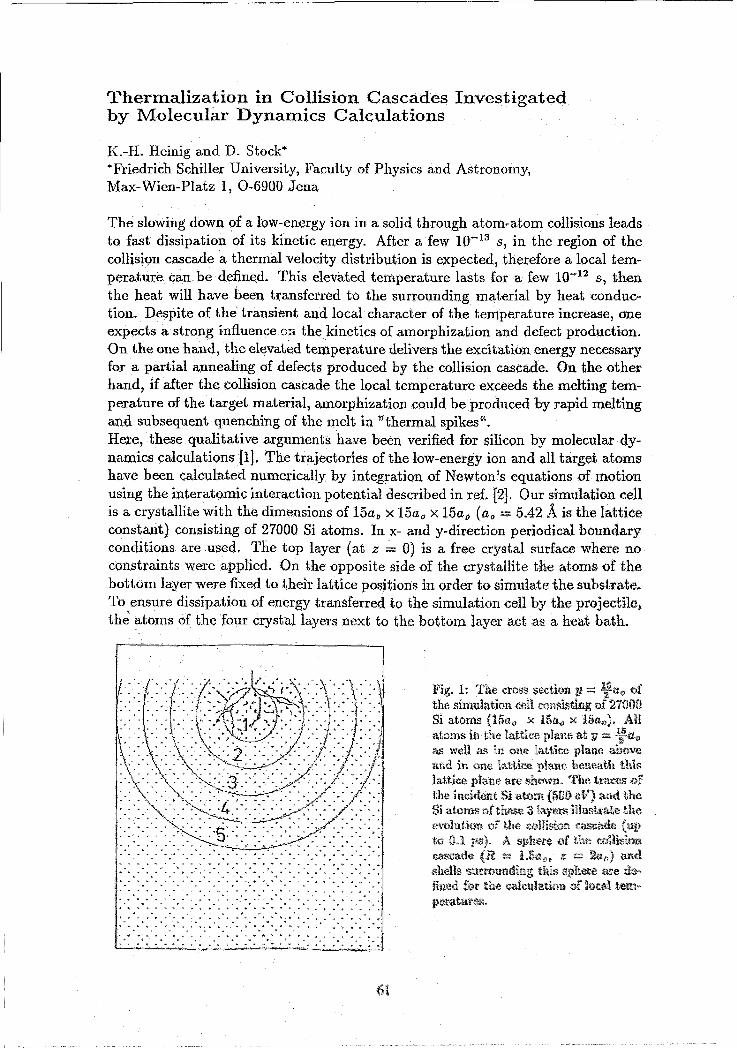
Thermalization in Collision Cascades Investigated by Molecular Dynamics Calculations
K.-EI. Heinig and D. Stock* *Friedrich Schiller University, Faculty of Physics and Astronomy, Max- Wien-Platz 1, 0-6900 Jena
The slowing down of a low-energy ion in a solid through atom-atom collisions leads to fast dissipation of its kinetic energy. After a few 10-l3 s, in the region of the collision cascade a thermal velocity distribution is expected, therefore a local tem- perature can be defined. This elevated temperature lasts for a few 10-l2 s, then the heat will have been transferred to the surrounding material by heat conduc- tion. Despite of the transient and local character of the temperature increase, one expects a strong influence sx the kinetics of amorphization and defect production+ On the one hand, the elevated temperature delivers the excitation energy necessary for a partial annealing of defects produced by the collision cascade. On the other hand, if after the collision cascade the local temperature exceeds the melting tem- perature of the target material, amorphization could be produced by rapid melting and subsequent quenching of the melt ia "thermal spikes". Here, these qualitative arguments have been verified for silicon by nolecular dy- namics calculations [ I ] . The trajectories of the low-energy ion and all target atoms have been calculated numerically by integation of Newton's equations of rnotion using the interatomic interaction potential described in ref. {2]. Qur simdation cell is a crystallite with the dimensions of 15a0 X 15a0 X 15a0 ( a o = 5,42 a is the lattice constant) consisting of 27000 Si atorns. In X- and y-direction periodical boundary conditions are used. The top layer (at z = 0 ) is a free crystal surface where no constraints were applied. On the opposite side of tke crystallite the aioms of %fie bottom layer were fixed to thei'r lattice pocitions in order ts simulate the substrats, To ensure dissipation of energy tranaferred ts the simulation ceZl by the proje~tile, the atoms of the four crystal layers next to the bottsm layer act as a heat bafh.

Fig. 1 shows a cross section of the simulation cell. The traces of the incident Si ion (500 e V ) and all recoils illustrate the evolution of a particular csllisisn cascade up to aboirt 100 fs after the ion impact. She initial temperature is T = 0 K'.
Fig. 2: Temperature sf the regions defined in Fig. 1 versus time for the particular collision cascade of Fig. 1. 10-l3 to 2 X 10-l3 s after the ion impact thermalizatisn is obtained, i.e, a local temperature can be defined. There are strong temperature fluctua- tions in region 1 due to the small num- ber of atoms ( las than 200). The tem- perature of the inner sphere remains for nearly 1 ps above the melting tem- perature (ca. 1680 I<). The longtime behaviour of the temperature corre- sponds to classical diffusion.
s imulation t ime (ps)
Fig. 2 shows the temperature in the regions defined by Fig. 1 for the particular collision cascade of Fig. 1. It should be noiticed that the temperature in the inner sphere remains above the melting temperature for nearly 1 ps.
Fig. 3: Plot of the statistics of tem- peratures for many collisiob cascades. The temperatures are calculated for the regions defined in Fig. 1. The cal- culation has been carried out for 25 different collision cascades produced by Si ions of E, = 500 eV with normal incident on the (100) surface, where the impact points were distributed over an elementary cell.
s imulation t ime (ps)
The featmes of t b callision cascades of different ions may be very different. For that reason, especially for the inner sphere different temperatiires are expected even for Ghe Same ion energy. Fig. 3 represents such statistics for 25 iori trajectories. It can be S ~ I I th& £W about 50 of the collision caccades t he temperature exceeds
temperahure. for s e tentli of a picosecond. Our recults should be a seliablie inapar t for tl~ermal spilce rnodels.

Cornpression Waves Induced in Si by Low-Energy Ions - a Molecular D ynamics S imulat ion
I<.-H. IIeinig and D. Stock* *Friedrich Schiller University, Faculty of Physics and Astronomy, Max-Wien-Platz 1, 0-6900 Jena
Some years ago Carter discussed the possibility of ion impact induced shock pro- cesses in solids [l] which are important for the sputtering yield. Using a semi quantitative model bis results are more or less On a qualitative level. We study the slowing down of low-energy ions in Silicon by full molecular dynamics (MD) calculations which is at present the most realistic method. Collective phenomena resulting from a collision cascade, e. g. shock waves and/or compression waves, are directly accessible by this first principle method. The equations to be solved and the ~otential taken into account are described in refs. [2,3]. Our simulation cell is the Same as in ref. [4]. Fig. 1 illustrates a typical compression wave found by our MD calculation. The simulation cell is viewed from the y- and x-direction (left and right part of Fig, 1, respectively). If we define that the center of the collision cascade is the origin of a co-ordinate System, then Fig. l a shows the radial shifts of the atom positions with respect to their positions before the ion impact. The 'radius of the atoms' in Fig. l a represents the amount of the radial shift, full circles mean atoms shifted away from the center, empty circles are radial shifts towards the center. The shell of shifted atoms (Fig. la) is surrounded by a shell of compression (Fig. lb, smaller interatomar distances). The wave msves with the longitudinal velocity of sound (vfloO' = 8400 ms-l).
Fig. 1: Snapshot at t = 0.5 ps of a compression wave produuced by a 500 eV Si ion (inieial position marked by a crsss) incident on a (100) Si surface.
(a) Radial shifts of the stom posi- tions, (b) J)evidion sf the ilocal mean interatomie distance irani the eqinlib- riurn value,

Molecular Dynamics (MD) Simulations of GRID Experiments
K.-B. Heinig and D. Janssen* "Institute of Nuclear and Hadronic Physics
Full MD calculations are the most realistic method to simulate the slowing down of low-energy ions in solids through atom-atom collisions [I]. Tke basic idea, of the MD calculations is that the positions and velocities of both the IOW-energy isn and the target atoms are calculated by numerical integration of Newton's equatisns of motion
dr; d ( m i v i ) r i j = V ; ,
d t d t (1)
where r;, V; and m; are the position, velocity and mass of atom i, respectively, and V(r) is the interatomic two-body ~otential. In view of the fact that the Si crystal consists of atoms held in place by strong and directional bonds, in sur case eqs. (1) become more complicated due to the use of pair and triplet potentials [2] for V < 0 eV. At V > 50 eV the strong chemical bonds become unimportant, kere we use an universal nuclear interaction potential [3]. The two regions are csnnected by a spline of fourth order. The equations of motion (1) were integrated in time using the Verlet algorithm in the velocity form. In ref. [I] we used this method to investigate ion implantation phenomena. Very recently, we applied our MD method to simulate 7-lines of recoiling excited nuclei [4], which are measured by the y-ray induced Doppler-broadening (GRID) method [5] . In the GRID method a recoiling excited nucleus is produced by the ernission of a prirnary y-ray of energy E, from the cornpound nucleus after thermal neutron capture. When the recoiling nucleus decays further by the emission of the secondary y-ray of energy E„ the measured Doppler shift AE7 of E, depends on the velocity v(t) of the recoiling atorn at the time t after the emission of E, and tke angle 8 under which E, is observed relative ta the recoil direction, i. e. AE, = i?:,P(L) cos I!?, where P(t) = v(t)Ic and c is the velocity of light. The Doppler broadened y-line contains information on the lifetime of the ~iuclear
or the stspping power of the recoiling atom in the solid, However, in s not possible to reprodiice the measured y-profile and to extract the life-
time of the nuclear state without a theoretical description of the collisions between the recoiling and the lattice atorris, Several procedures of theoretical analysis are ctnrrenhly agrplied to khe GRID data, the most appropriate MD method has been employed for the Erst time by Kuronen [6]. Improved lifetimes of excited nuclear states ctrid fircst experinsentaH infosrnation on the interatomic interaction potential
of a few EOO eV Hnave been obtained. een xsnnrried [G] that, as tlre direction of the primary 7-i-ay is
isskogicdly dictriibuited, is n d fixed by the experirnent and thus does not enter explicitiy, Thon onr: abdains for the Doppler-broadened line shape

Bere I is the intensity of secondary y-rays with Doppler shift AE, = E,v/c, t„, is the time up to which the simulation events are calculated, T is the lifetime of the nuclear level under study, and V„, is the maximum velocity of the recoiling atom, The distribution function f (V, t) of the absolute values of velocities is obtained from the MD simulations. Tn ref. [7] , for polycrystalline titanium measured lineshapes are compared with lineshapes calculated with eq. (2). The smooth shapes of the line profile allow the fit of one quantity at best, in the actual case the lifetime of the nuclear state. I£ another interatomic interaction potential is taken for the MD simulation, the fit gives a modified lifetime. To fit both, lifetime and potential, for a transition a more structured lineshape or a series of lineshapes is necessary but not available by this procedure.

Recently, we predicted for the first time y-lineshapes for single crystals [4]. Up to now no experiments have been carried out for single crystals [8]. We use
where AE, = E - E,. Our more general formula (3) csntains the direction sf the spectrometer axis n (with respect to the crystal axis) an61 all velscity vectors vi(t) of the recoiling atoms i. Using our MD code, we simulate for the nuclear re- action 28Si(n, y) 2"Si the profile of the Doppler-broadened y-line of the secsndary y-transition with E, = 2.43 MeV and T = 10 fs, where the Boppler-braadening Comes from the primary y-decay with E, = 6.05 MeV. In our MD simulations, the recoil atoms start from a lattice paint into 3000 ran- domly distributed directions. The slowing down of the recoils is calculated using a finite cell of 960 atoms with periodical boundary conditions. The crystal structure is of diamond type. After each time step tj at the Doppler shift AE, = vi(tj)ri/c the value P j = e-tjl' has been added to the intensity I(AE7). This procedure is equivalent to the calculation of T(AE,) corresponding to eq. (3). Our theoretical prediction proves that considerably improved GRID experirnents can be carried out with monocrystalline samples. Then different crystal align- ments lead to different lineshapes with a pronounced structure (see Pig. 1)- These lineshapes contain sufficient information to fit several quantities (e. g. lifetimes, potential) in one experiment. Fig, 1 demonstrates that even small differentes in potentials should be measureable in the energy region 50 eV < EI < 1 keV, where other methods fail to give good results. After the reconstruction of the research reactor at the ILL Grenoble our proposed experiments will be carried out [8]. The new ultra-high-resolution gamrna spectrometer GAMS5 should even allow to de- termine the location of impurities in a host crystal. This work was supported in part by the Bundesministerinm für Forschung und Technologie under Grant No. 211-5291-03-HE3ROS.
References
K.-H. IIeinig and D. Stock, to appear in Niicl. 'Instr. and MetIi.; D. Stock and K=H. Heinig, MRS Fall Meeting, Symposium A Bearn-Sohd Interactions: Fandanzentals & Applications, Boston, USA, Nov. 30 - Dec. 4, 1992, contr. paper A7.11. F.11. Stillingx and T.A. Weber, Phys. Rev. B31, 5262 (1985).
er, $ 2 . Biersack and U. Littmark, The Stopping and Range of Ions in Solids, Press, New York,1985).
X.-H- Heinig and D. Janssen, in: Workshop on Applications of High Resolution Siudies of Atomzc Collisions und Nvclear Lifetzmes, eds. II.G, Börner, 3. Jolie, M. Pendlebury, and S. Ulbig , Inv. contr.;
to nppear in Phyc. Letter$. „ Bfnsnrer, J. JaPie, P. Hqler, S.J. Robinson, M.S. Dewey, G-L. Green, E.G. Kessler, and
f3eslattec, Phys. Lett. B215, 45 (1988); ie, S, UPbPg, N.G. BGrner, K.P. Lieb, S.J. Robinson, P. sdiillebeeckx, E-G. ICessler,
M.S. Dewey, an$ G L Greene, Europhys. Leht. 10,231 (1989). A. Kuronen, 3, Ptips. G3, B1 (1991); A. Kürelnen, 3. KeSkronctn, B.O- Börner, J. Jolie, and S. UEbig, Nucl. Physics A549, 59 (1992)- A. Kuroaern, J. Phys. ondenc, Matter 3, 1563 (1991). 1I.G. BErnm, private eommuiii~atioii.

The Diffractometer of the RCR at the k e i Reactor
A. Mücklich, M. Betzl, P. Reichel, and W. Bode
After the final decision for shutting down the Rossendorf Research Reactor (RFR) a neutron diffractometer was installed at the Re2 Reactor (RR) by the Research Center Rossendorf (RCR). The RR providing a sufficient thermal neutron flux of 5 X lO*~m-~s-' at its channel is of the same type as the RFR and allows therefore the use of existing parts of diffractometers situated at RFR before.
It was the intention to set up a conventional neutron powder diffractometer containing attachements for a quantitative texture analysis. Moreover measurements of geological specimens which cause a large secondary beam should be possible. The diffractometer TEXDIFFK9 was moved to RR after performing a complete upgrading of the instal- lations. This includes the conversion to new electronics for registration and controlling (PC 386SX) the software of which was elaborated in the months before. Moreover TEXDIFFK9 was equipped with an Eulerian cradle of the large HUBER type with 0 400 mm and a gap of 127 mm. The step motors used allow rotations with a reproduci- bility better than 2". Immediately after transport the building up of the equipment at horizontal channel HK6 of the RR was started. Here the very time-consuming erection of the completely new designed shielding walls consisting of boron-polyethylen blocks has to be emphasized. For generating a useful initial neutron beam divergency (= 1 ") three collimators were installed into the closing system of HK6 (0 60 mm). After that the mechanical and the optieal adjustment of the basic device was carried out. Hence it followed a limitation of the scattering angle at 28, = 114", where the detector and the monochromator shieldings touch one another.
Simultaneously with the beginning of the first cycle after the reactor rest in the summer period, we were ready to start the neutronographic adjustment. By means of Ni powder standard a wavelength X,= 0.144 nm could be determind for the (W2)-latticc plane of a Zn monochromator. Via Q = 4mineJX it conesponds to GX = 73 nm-l. Iri Table 1 spacings, wavelengths and Q-values are given which bmome relevant if other rnonochrornator materials as pyrolytic graphite (PG) or copper are usd.
Taking into account the mosalc sprwd of the rnonochromatm bei divergency of the coilimator (A29 = 28") in front the 3E.Ie d resolution Adld I 2.8 X was achievved wbkh Ps relativ lurninosity. The background counting rate is sufficlently sm the whole arrangement at HK6 is given in Rg, I, Xt dem measured a t points indicaterrl as that of the iowesk md cabin, are very IO~U for bot8 neutron and y*radiatitsn*

Fig. 1: Top view of the diffractometer at HK6 of RR
Bisregarding a break of a week in December caused by an error in the controlling System the running of the diffractometer could be achieved for all reactor cycles in the last quarter of 1992. The distributian of measuring time was planned in a multi-user regime in which the RCR, the TU Mining Academy Freiberg, and the Geological Research Centre Potsdam were involed. Consequently, beside methodological problems the textures of both metallic (Fe sheets, brass tubes) and geological (Hatite) samples were investfgated.
The diffractometer at the RR is already a fully established equipment the using of which is apen for German and Czech scientists. Thus, one of the new Users starting in spring 1993 will be thhe TU Chemnitz the activities of whorn wilI be focussed on the stmcture (05 malten alloys. For 1993 the intention is to convert the detection to a position-sensitive System of the JULZOS type, Moreover a PC 386DX exclusively for da& evaluat5sn wili be installed.

Neutron Diffraction Analysis of Siihstrrictiires in Polycrystalline Materials
P. Klimanek*, T.Kschidock0, A.Mücklicli, P.LukasM, P.Mikula**, M. Vrana" 'Department of Materials Science, TU Miiiing Acadeiiiy FreibergISa., P.O.Box 47, DO-9200 FreibergISa., FRG "Nuclear Physics Institute of the Czech Academy of Science, CR-250 68 Rez n.Prague, CR
Introduction
The mechanical properties of a polycrystalline materia! strongiy depend on its substriic- ture. An integrated substructure analysis (i.e. analysis of lattice disorder of the 2nd kiiid due to structure defects as dislocations, stacking faiilts etc.) is often performed by evaluation of the line broadening of X-ray diffraction peaks ([1,2,3'j for instance). In this connection two difficulties have to be taken into account : - the lirnited number of grains contributing to the observable line shape and broadeniiig
and, consequently, to the orientation averagin~g over the lattice disorder of the iiidi- vidual crystallites, and
- the strong decrease of the X-ray scattering intensities at higher diffraction ailgf-ss which significantly complicates the detection of weak physical line broadening (or small level of lattice disorder, respectively).
Both problems c a . be avoided by use of elastic neutron scattering. It allows averaging over a large nurnber of crystallites ,and secoiid, tlie atamic scattering power of the sain- ple material is, as a rule, independent of the scattering angle. Therefore shape aiialysis of physically broadened neutron diffractioii pe&s should be an attractive suppleiiient of the procedure of integrated substriicture iiivestigation. Of Course, becaiise of tlie in- strumental line broadening of the refiection due to non-ideal diffraction coiiditioiis, iip- plication of high-resolutioii neutron diffractoinetry is necessary for this piirpoäe,
Experimental Procediires
Eqiii~ment: The present work was perforiiied at tlie high-rcsolution triple axis iietttrt)n spectrometer TKSN 400 of tlie NucIear Physics Iristiliit Rez (11. Praguß,{7f)- Beam monochromatisation aiid analysing uses benl Si(220)- ~rystals. "l%e registralion riiode was 8-28-step scanning with a step size AB 4 . O I 8 " .
Saniple material: For the experiments teclinicalty pure capper arid a X CzNWi 18.7 skei were chose~~. After annealiiig both in als wetz plastieafly ilefc~rin by coinpressio~~ at room ternperature (E„-%? 94, E„,*- ], During tlic defc>ri.i~atiuir the sied k ~>;trtiri!ly transforined into ciibic iiiartensite, Material of standards were annealed at 7i)O"Cif2UriiPii (Cc~pp~r) atid iron) tu geet the reqiiired structure.

Experimental Results and Concliisioiis
In Fig. 1 the (110)-diffraction line shapes as obtained by X-ray and neutron scattering are compared. The graph demonstrates the equivaleiice of the data and the excelleiit resolution of the neutron spectronieter used.
Fig. 1: (1 10) diffraction line profiles of niartensits as nieasured with X-rays (a) and neutrons (b)
Table 1: Structure Parameters of copper and tnartensite

The substructiire Parameters calculated froiii Warren- Averbach and Krivoglaz-Wilkens plots of the Fourier coeffizients I4,5,6] are given in 'Pable 1. Taking into account [hat the step size of the neutron diffraction experiiiien[ iiiust yet be optimized and tliat the number of scattering crystallites is very different in X-ray and neutron diffraction , the agreement of the data is satisfactory. A good correspondeiic to substructure paraineters determined from X-ray diffraction is also given in the case of copper.
* * *
The present work is supported by the Federal Ministery for Research and Technology (BMFT) of the FRG.
References
[I] Warren, B.E.: Progr-Mehl. Phys., 9, 147 (1969) 121 Klimanek, P.; Freiberger Forschungsheft B 132, 33-65 (1968) 131 Delhez,R.; de Keijser, Th.H.; Mittemeijer, E.J.: Freseniiis 2. Phys. Ctiern., 312, 1 (1982) 141 Krivoglaz, M.A.: -Theory of X-ray sand thermal neutroii scattering by real crystals (in ntss.),
Moscow 1967 -Theory o f X-ray and neutron diffraction by imperfwt cystüls (in russ.), Kiev 1983
[SI Wilkens, M.:-phys. stat.sol.(a), 2, 359 (1970) -in: Fundamental Aspects of Dislocation Thaory (Editors: J.A.Simmona et al.), Vol, 11, 1195, N.S.B. Special Publ. 3 17, Washington 1970 -Kristall & Technik, 11, 1159 (1976)
[6] Klimanek, P.:Freiberger Forschungsheft B 265, 76-91 (1988) in:X-ray and Neutron Structurz Arialysis in Material Wsrarch (Ed, J.Hasek), Plenlrm Pt&$, New York 1989, 125-137 in: EPDIC 1-European Powder Diffra~tion(Ed. K. Dellic;~, E.J. Mittemc;iJer), Mat,Sci.Fonim 79-82, Pt, I, (1991)
(71 Kulda, P.; Mikula, P.; Lukas, P.; Kocsis, M,; Ppoc. int.ConL Neutron katiri.riny, Oxford, Physika B (1991)

Study of Hardening of Portland Cement Paste by Small-Angle Neutron Scattering
F. Eichhorn, F. Häußler*, and H. Baumbach*"
"Institute for Nondestructive Testing Saarbrücken (FhG), at present: Frank Labora- tory for Neutron Physics of the Joint Institute for Nuclear Research Dubna, Russia
""Institute for Nondestructive Testing Saarbrücken (FhG)
Building materials like hardened (hydrated) cement or concrete are heterageneous. Especially for such substances their useful properties (as strength, porosity, thermal insulation, permeability for gases and liquids) are determined by the structure within and between tkzir components. The development of the material structure during .the hydration process depends on the starting values (composition of the mixture, for instance the mass ratio of water to cement or the content of additives) and on the externai physical Parameters and technological conditions of the process (e. g. tempera- ture, humidity, vibration).
To observe the mesoscopic structures in an averaged way the method of small-angle neutron scattering (SANS) was used with its possibility for contrast variation between different phases of the hydrating material. Hydration with H,O, D20 or a rnixture of them, respectively, gives various values of the scattering length density.
Here results of an ordinary PortIand cement (type 1/40 A) are presented which are obtained by the MURN device at the IBR-2 pulsed reactor of the JINR Dubna. SANS curves are measured in the scattering vector range between = 0.00863 A-' and aa, = 0.147 A-' (Q = 4?rsine/X, 2 8 - scattering angle). According to the sampling theorem [I] reliable results from this measuring conditions can be obtained for spheri- cal particles with gyration radii between 8 and 141 A.
For the present investigation the samples of hardened cement paste are prepared from ordinary Portland cement (OPC) and heavy water @,O) with a water-cement ratio of 0.38. For these preparation conditions the most abundant hydrated cement phases C3S2 = 2 . 5 ~ (content 45 %), Ca(OH), (22 %) and C,A * CaSO, 12w (17 %) give the maximum contrast with the Pore system (C = CaO, S = SiO, , A = AlD, , and W = water) E21 . The thicknesses of the specimens used were 0.50 mm, 1.05 mm, and 1.70 mm. The Figure 1 shows the measured scattering Cross sections for the specimen of 0.5 mm thickness.
Assuming a logarithmic normal distribution for the size (geometric radius R) of spheri- eal pärticles (pores or grains of different phases)
the most probable radius R, (ccntre of the distribution ) an$ the dispersion s f that dist-ribution (p - FWHM) are given in rhe T&le 1.

4
I rb
HYDRATING CEMENT PASTE 10 ] CP190392(1-1)
k d a
(thickness 0.50 mm) r o o o ~ o 33 hours old -
I I
0.01 0.1
Q / A - ~
Fig. I : Small-angle scattering cross section ofa hardening paste of ordinary Portland cement. The curve parameter is the time aftcr thc begiming of the hydra- tion
Tab~. 1 : Parameters (the most probable radius K, and the FWIIM) of a logarithmic normal distribution for spherical particles in dependence on the hydration time iof a Portland cement paste
The results show that the mean partide size reaches I& Gnal vdue dready in the ewly stage of hydration whereas the dispersion of the partiele size increases during a h g e r period.
Analyzing the scattering cross section at higher values of Q a deviation from the Fora& law (valid for compa~t particles with sharp bounidaries) is obsemed, This may 'be eaused by a fractal-like surface or valurne structure f3] , To study thia groblern further In- vestigations are in preparation.

Studies of Sr,Ba„Nb,O, Mixed Crystals by Neutron Diffraction at Temperatures between 15 K and 293 K
F. Prokert and B. N. Savenko*
*Lab. of Neutron Physics, Joint Institute of Nuclear Research, Dubna, Russia
At the time-of-flight (TOF) spectrometer DN-2, installed at the pulsed rac tor IBR-2 in Dubna, SrxBa„-xNb,O, mixed single crystals (SBN-100x) of different compositions (0.50 I X I 0.75) were investigated in a temperature range between 15 K and 293 K. The diffraction Patterns are taken along the directions [OOlJ, [I 101, [I 111, and [lOO] from a sectorial area of the scattering plane (110) and (OOl), respectively.
The temperature dependence of the Bragg intensities as well as that of the lattice spacings show an anomalous behaviour. In Fig. 1 and Fig. 2 this is illustrated for the lattice parameters C and a. These data are collected from a SBN-70 crystal in TOF scans which were directed along the two basic directions. In extended regions anoma- lies of the thermal expansion are indicated by the slope of these curves.
Fig.1; T~eniperature d~pendence of the lattice Parameter c obtained from [OOl] scans on SBN-70 (D) - eooling from room temperature @T) after a heating pretreatment (2h at about 600 K) (8) - heating-up to RT

SBN-70 [l00] Scan
Fig. 2: Dependence of a relative lattice spacing (a/am) on tempemture obtained from [IOO] seans on SBN-70 at repeated cooling - heating cycle (0) - cooIing-down from RT (sample initially pretreated as described above) (X) - heating-up to RT
Besides the known phase transition at about 190 K [I] a d at about 60 K 121, which are clearly visible by anomalies at the most scan directions, in different scans another structural change occurs at about 250 K. In regions aroutld these tmnsitions the Bragg peak intensities as well as the lattice spacings show a large temperature hysteresis, an$ the widths of the Bragg peaks reach extremal values.
It is well-know, that the highly disordered relaxor material 53324 at higher temperatuaes undergoes a diffuse ferroelectric phase transition [3]. Additionally, in the invesdgat& lower temperature range m influence of electric field cooling on the diffraerlon pattem, checked. at SBN-70 along [110], is found. Further, the investigated struetur@ chmg"3s are sensitive to the thermal or electric sample history. These facts agrm with sp tions about field-induced orientation processes of 'fruzen-in'polar irl.usters D] and could fit into the picture of a change s f pslarization at bw temperatures due to ucctn- rence of a L1 101-component in ttie spontaneous polarimtion [2j.
This work has bwn supporEd in part by the 3Mf;"f under registration nurnber G03ROS-5,
References Ii] L. 19, BursEil arrd Peng 1x1 Lin, Acta. Cjryst, B43, 49 (Cf
€33 B* N. SavenPi:~~ B. Sangaa, P, BrolkePt, F2:rci>sI%tn~~ 1@2,

The Neutron Time-of-Flight Diffractometer NSHR at IBR-2 in Dubna
J. Heinitz, K. Ullemeyer, and K. Walther
In order to improve technological processes or the properties of materials one has to consider the real structure of the (polycrystalline) material like grain size, grain bounda- ries or grain orientation. In material science the investigation of the preferred orientation began more than 70 years ago and the engineers have accumulated a lot of experience to solve the most problems connected with the development of the texture during processing. In natural objects preferred orientation of its structural elements also occurs. For instance, at geological formations this oriented structure is looking like foliation, lamination, folding etc. Because these structures can have gigant sizes and can be Seen by unweaponed eyes they are described qualitativly more than 0r.c century ago before the development of powerfull microscopes or X-ray diffractometers. The quantitative description of the dynamical processes within the lithiosphere and of the development of the texture are delayed in comparison with the materds science. For the investigation of geological samples one has to overcome some difficulties: 0 Most geological samples are coarse grained and inhomogeneous. The investigation
of the texture requires the use of neutron diffractioin. 0 Because of the low crystal symrnetry the diffraction patterns show many peaks which
are often overlapped. A diffractometer with a high resolution is therefore necessary.
A neutron time-of-flight diffractometer has been Set in operation at a long flight path (104-66 m) at the 7' beam of the pulsed reactor IBR-2 in Dubna, Russia. This Neutron Spectrometer with I g h &solution (NSHR) is mainly used for texture investigations. -
Fig 1.: The tayour of the diffractorneter NSHR at tlie bieam 7A of the reactor IBR-2. (1) core of the reactor; (2) moderater; (3) reactor shield; (4) bearn lock; ( 5 ) disk chopper; (6) biolqieal shield; (7) first part af the neutron guide, Ar-filled; (8) second part of the aleutron guide, vacuum; (9) detector shield; f 10) texture goniometer; (1 1) platform, turnabl e; (1 2) b a e of die diffractometer; (1 3 ) beam sitop.
The layout is shown in Fig. I. After escaping the core (1) the fast neutrons are slowed down to thermal energies in a lig11t-water t-noderator (2). An additional disk chopper (5) werking synchronously with the reactor reduces the background between the reactor

pulses. 'The neutrons are guided by a Ni-coated straight neutron guide (7,s) to the sample fixed in a goniometer (1 0).
The diffractometer is equipped with a central sample desk carrying the goniometer or other sample environments like a furnace. Seven detectors in detector shields (9) are mounted on a moveable platform (1 1) achieving a wide range for the scattering angle 28 from -lOQ to 190". The minimal angular distance between two detectors is 14" in the 28-scale.
The Cross section of the neutron beam is 50 x 170 mm2 and the flux of thermal neutron is greater than 1 x 10% nm-'s-'.
The diffractometer is remote controlled by a PC/AT via CAMAC-Interface. Step motors serve for a high precision in angle setting. The samples should have a spherieal, cylindrical or c&ic shape with a dimension of about 2.5 cm.
The good resolution and the relatively high neutron flux make the diffractometer very suitable for texture investigation of geological samples. Fig. 2 shows a diffraction Pattern of quartz powder. The scattering angle 28 was 160" and the measuring time 2
Quartz Detector A - (2+= 1 60°)

applicable an uniaxial load with forces of 10' N at temperature up to 1000 K. In the other cell in addition to the uniaxial load a hydrostatic pressure up to 15 khar will be available, but the temperature exceeds only 600 K. The sample volume is about 5 cm3. Several Sensors are fixed at the sample in order to measure the strain rate, the sound velocities and the acoustic emission during the deformation. Mainly these high-pressure devices will be constructed for the investigation of phase transition and the orientation relation between the a- rsnd ß- phases in quartz .
In order to minimize the experimental effort the detector arrangement should be changed that all detectors form a cone with the same scattering angle. At optimally chosen scattering angle the sample movement can be reduced to rotations about one axis only.
In Table 1 the characteristics of the diffractometer are compiled. A great spectrum of geological specimens was studied: sarnples from the super-deep drilling boreholes in Windisch-Eschenbach (Bavaria) and Kola (Russia), feldspars, micas, olivines, hornblendes, and other low-symmetric minerals.
Table 1: Characteristics sf the diffractometer NSIHR
Beam Beam Cross section Chopper Moderator-sample distance Mean fiux of thermal neutrons at sample position Wavelength Scattering angle d-spacing (at 28 = 60") Resolution Adld, (28-1 60D, d > u ) Number of detectors Type of detectors
Sample environment
Experiment control
Ni-coated straight neutron guide, total length 92 m 50 X 170 mm2 at 5.50 m from the moderator 103.06 m 2 1 X 10⁶ n S"
0.8 - 7.6 -10" - 190" 0.8 - 7.6 A 0.4 % 7 3 He-counters, 1.7 crn 0, 25 crn length, battery of 5 Counters texture goniometer, furnace (T= 1000 K) high temperature press (planned) PCIAT with CAMAC-controller

7.25 GHz ECR Source for Highly Charged Ions
R. IIentschel and 13. Tyrroff, L. Friedrich*, E. Huttel* and L. Wiss* *Kernforschungs7xntnim Karlsmhe GmbH (KK)
A 7.25 GHz ECR ion source formerly delivering strong ~ e ~ + bearns at KfK was modified and aptimized to create well resolved beams of highly charged, slow ions to be used for atomic and surface physics research at Rossendorf [I]. The final setup of the magnetic eiements generating longitudinal and radial field components, the R.F. feed, an additional electron emitter, and the ion extractisn System are shown in Fig.1. In this figure the on axis longitudinal distribution of the magnetic flux den- sity for a typical excitation current (820 A) is displayed, too [2].

Fig. 2: Multipole cross section (sinalter diameter corresponds to dkcharge vessel, pole size and remanence (NdFeB) indicated), radial component of flux density Brad(r) at azimuth = . 0,6,12,..30° and total flux density Bsum@hi) at radii = 0.5,1,1.5 ,... 4.5 cm [3].
At Eirst, the positions OE longitudinal field coil packages and magnetic shim inside the retum yoke were optimized. Further, the best position of the longi- tudinal field to the ion extraction System was found. The electron emitter consists of a cylindricaI, insulated aIuminium block, beeing charged to potentials between -5 and -10 V by the discharge itself. The best longitudinal position of the block was found experimentally. Using the emitter the ion current of highiy charged nitrogen or argon ions was increased by at least a factor QE two. Charge distribution spectra have been investigated by a stigmatic 90" analyzer magnet ( bending radius 200 mm, mapifieation I), image slit (width 10 mm) and Faraday cup. Tab.1 and Fig.3 illustrate resuIts of opti- mizing gas pressure, longitudinal field excitatiorr, and R.F. power and gas mix-
Tab. 1: Charge states and dorresponding ion eurrents C?" mearrs interference with 1PU-X es).
Nitrogen &. Helium
I 9.3 2 f 3 17.3 4 26 5 23 B 5 7 7

ing for high charge states. The source is installed at Rossendorf now. We intend to inflect Z/A resolved beams by a spherical condenser into the beam line of the Van de Graaff accelerator and to decelerate the ions on their way to the target station to kinetic energies of about 11100 of the Start value (Fig. 4). In this way the ion's kinetic and potential energy (potential energy represented by the charge state) at the target can be choosen independently .
pnalyzer nagnet
Fig. 4: Proposed experimental setup of ECR ion source and V.d,GraaE beam line at Ro8sendorE
Acknowledgements
This work is supprted by BMW 06 DR 308 and Volkswagen-StiBung R.H. and H.T. thank C. Neelmeijer for stimulating discussions.
References
[I] R. Grötzschd, C. Neelmeijer, H, Tyrruff, f31. Büttig and LS, Prtrusciie, FSR 92-06,6S, rtossendor
[2] EX thanks Michaef Schl [3] cafculated on the base of

Improvement of the Experimental Possibilities at the 2 MV Van de Graat'f Accelerator
~ W. Bürger, M. Friedrich, R. Grötrschel, C. Neelmeijer, and S, Tumc
The 2 MV van de Graaff accelerator has been equipped since its starting 1963 with only one beam line. This does not allow any separation of experiments with high and ultrahigh vacuum.
During the out of operation period 1992 a switching magnet with +15' and -10" deflection was installed (see fig. 1 of tandetron status report). The RBS chamber is placed at the 10"-beam line and an ultrahigh vacuum equipment was built up at the 19-beam line. The belonging experiment chamber has been placed at our disposal from the group of Prof. Sitzmann from the Ludwig Maximilian University Munich.
Beside the high energy ions from the accelerator also highly charged ions from an ECR ion source will be injected in this chamber for surface investigations. Both beam lines has been put into operation in February 1993. The energy stabilizing system of the accelerator has been improved by installation of a new NMR device at the analyzing magnet made in the Institute of Nuclear Research Rez of the Czechoslovacian Academy of Sciences.
Status Report of the 3 MV Tandetron
M. Friedrich, S. Langer, S. Tumc, and E. Wieser
A contract for installation of a 3 MV tandetron (high current version) was made with High Voltage Engineering Europa B.V. at the end of 1991. The iandetron will be applied mainly for high energy implantation. First experiments have been made already at the 5 MV tandem accelerator, but the beam current of this accelerator is not sufficient high for routine implantation. Beside the implantation beam line a chamber for routine RBS-measurements and a nuclear rnicroprobe will be built up. The 3 MV tandetron will be installed in the second experimental room of the 5 MV tandem accelerator, the experiments will be arranged in a separate room (see fig. 1).
The direct vicinity to the other eleetrostatic accelerators allows the operation of the tandetrun by the already existing accelerator staff. The chosen arrangement minimizes the s täff arid building expendittture,
The maln aetiviities in 1992 wert: directed to reaiize the instalP~tion requirements of the caoPing water, eIectric. power, air-eonditioning and room-preparation). These
activities were finished in Eebruary 1993.


Developments for the Accelerator Control and Stabilizing Systems
W. Bürger
The time of the accelerators shut down was used for extended technicai modernisation and development at the accelerators. This work was mainly directed on improving the accelerator control under the condition of reduced staff and on providing for the stepwise application of a modern Computer system.
2 MV Van de Graaff accelerator
The vacuurn control system Las been improved in connection with the installatici~of new vacuum pumps. Activities at the charging current stabilizing system were directed on the increasing of the signal/noise ratio of the charging current measurement. At the analyzing magnet a new NMR device was installed, which is of the same type as the NMR device at the tandem. The devices were developed and produced at the Institute of Nuclear Research Rez of the Czechoslovacian Academy of Sciences, They are microprocessor controlled and allow automatic magnet formation and signal finding.
5 MV Tandem accelerator
The installation of a new power supply system for the ion sources was started using a programablle control unit SIMATIC S5 115 U (SIEMENS). For our sputter ion source these activities have made a large Progress and the corresponding preparations for the duoplasmatron have been begun. All ion opticai ekments now are equipped with high stabilized power supplies. The transmission of analog control and measuring values across distances of more than a few meters is now done by using symmetric lines for improving the siinallnoise ratio. The energy stabilizing System was comprehensively revised. Investigations in the behaviour of linedrized corona triode amplifiers with either current or voltage feedback were done but are not yet finished. Preliminarily it a n be said that in dependence of the parameters of the accelerator (in particular in dependence of the relation of the accelerafion voltage fluctuation caused by corona instabilities to tkdt caused by the charging) &her the current or the voltage feedback gives better stabilitiy and resporise. The lang-time stability ofthe pick-up amplifier has been improved on the base of modern integrated ~ircuits. As sIit amplifiers linear amplifiers with remote controlled gain are generaliy used now (contrary to the Iogarithmic amplifiers common in uthers laboratories). we have tmegun to revise the gcnerating voltmeter with respect to the conditions of accelerator mass spectrometry operation. The main goals of this work are
- simple n<jjustnment of the mechanical patt of the device - high suppressi~n of electromaznetic interferences - high uppeic 1imi.tEng Frequency csf die voitage measurement.
In the deviee conventicrnaf anajog components are used in the processin; of the sensor p&ak chinrernk

Publications
Brauer, G., Matz, W., Liszkay, L., Molnar, B., and Krause, R., Positron Annihilation and Mössbauei Studies of Neutron Irradiated Reactor Pressure Vessel Steels, Materials Science Forum, 97-99, 379 (1992)
Eichhorn, F., Podurets, K. M., Shilstein, S. SR., and Soroko, Z. N., Surface X-Ra y and Neutron Scattrering, Springer Proceedings in Physics 61,251 (1992)
Erokhin, Yu.N., Grötzschel, R. Oktyabrsky, S.R., Roorda, S., Sinke, W., and Vyatkin, A.F., Mesotaxy by Ni diffusion into buried a-Si layer, Mat. Sci. and Eng. B12,103 (1992)
Erzgräber, H. B., Zaunseil, P., Bugiel, E., Sorge, R., Tittelbach-Helmrich, K., Richter, F., Panknin, D., and Trapp, M., Properties of the TiSi2/p+n stwtures formed by ion implantation through silicide and rapid thermal annealing, J. Appl. Phys. 72, 75 (1992)
Grambole, D., Herrman, F., and Klabes, R., Investigation of oxygen and fluorine distributions using nuclear reaction analysis at the Rossendorf nuclear microprobe, Nucl. Instr. and Meth. in Phys. Res. B64, 399 (1992)
Grambole, D., Herrmann, F., Klabes, R., Hauffe, W„ and Behrkch, R., Investigation of the deuterium distribution in a JET limiter using the nuclear microprobe and ion beam slope cutting, Nucl. Instr. and Meth. in Phys. Res. B68, 154 (1992)
Grötzschel, R., Hentschel, E. Klabes, R., Kreißig, U„ Neelmeijer, C., &smann, WW5 and Behrisch, R., Elemental analysis of thin layers by elastic heavy ion scattering, Nucl. Instr. and Meth. B63, 77 (1992)
Helming, K., Voitus, W., arid Walther, K., Progress in texture investigations at the pulsed reactor ZBR-2 Physica B 180 & 181,1025 (194'2)
Henke, B. and Hentsehel, K„ An ECR Ion Stwce h r Ion IrnpIantatian, Rev. Sci. lnstr. 63,253
Hentschel, R. and Henke, D, Uxygen and Carbon Ions h r n a Reflex Ion Sourlirr, Rev. Sci. Instr- 63,2590

Jäger, H.-U., Modelling of the formation of buried dielectric layers by ion implantation, Nucl. Instr. and Meth. B65, 67 (1992)
Kurbakov, A.I., Rubinova E.E., Sokolov, A.E., Mäder, M., Tempel, A., ancl Tobisch, J., Gamma-ray diffraction study of MBE grown CaF2/Si(lll) Heterostructures, Cryst. Res. & Technol. 27, 791 (1992)
Küchler, R., Ultrasonic Surface Waves for Studying the Properties of Thin Films, Phys. stat. sol. (a) 132, K65 (1992)
Leiss, B., Voitus, W., and Walther, K., Neutronentexturanalyse von Dolomitmyloniten aus dem ~amara-Orogenmamibia (Teil I), Frankfurter geowiss. Arbeiten, 11, 120 (1992)
Leiss, B., Helming, K., Siegesmund, S., and Weber, K., Neutronentexturanalyse von Dolomitmyloniten aus dem Damara-Otogen/Namibia (Teil 2), Frankfurter geowiss. Arbeiten, 11, 253 (1992)
Lohner, T., Skorupa; W., Fried, M., Vedam, K. Nguyen, N., Grötzschel, R., Bartsch, H., and Gyulai, J., Comparative study of the effect of annealing of nitrogen-implanted SOI-structures by spectroscopic ellipsometry, XTEM and RBS, Mat. Sci. and Eng. B 1 5 177 (1992)
Matz, W. and Wieser, E., Konzeption für ein Strahlenforschungszentrum Rossendorf, FZR 92-04, Rossendorf, März 1992
Matz, W. and Einfeld, D. (verantw. Bearbeiter), RBSY - Rossendorfer Synchrotronstrahlungsquelle, FZR 92-10, Rossendorf, Juni 1992
Meelmeijer, C., Grötzschel, R., Klabes, R., Kreißig, U., Müller, W„ and Kruschke, D., Simultaneous analysis of Li and B in amorphous thin film glasses using ERDA, Nucl. Instr. and Meth. B68, 231 (1992)
Panknin, D., Richter, F., Bugiet, E., and Erzgräber, H., Formation of titanium silicide during rapid thermal annealing: Influence of oxygcn, J. Appi. Phys. 7 5 815 (1992)

Panknin, D., Wieser, E., Gr6tzsche1, R., Skorupa, W., Baither, D., Bartsch, H., Querner, G., and Danzig, A., Ion beam synthesis of burield FeSi2 in (100) silicon, Mat. Science and Engineering, B12, 119 (1992)
Pham, M. T., Characterization of ion-implanted gate insulator films for use as ion sensitive membrane in ISFETs, Sensors and Actuators A, 7, 576 (1992)
Pham, M. T., Hoffmann, W., and Hüller, J., Thin insulator films chemimlly sensibilized by ion implantation for application to ISFET microsensors, Sensors and Actuators B, 8, 227 (1992)
Posselt, M., and Biersack, J.P., Computer simulation of ion implantation on into crystalline targets, Nucl. Instr. and Meth. B64, 706 (1992)
Posselt, M., Drechsler, L., Grötzschel, R., Klabes, R., Otto, G., Schöneich, A., Sobeslavsky, E., and Syhre, H., Particle reflection and reimplantation during grazing incidence implantation of As+ and B+ into silicon, Nucl. Instr. and Meth. B67, 443 (1992)
Prokert, F., Balagurov, A. M., Savenko, B. N., 2nd Seglins, J., TOF Neutron Diffraction Studies on Weakly Doped Single Crystals of SrXBal-,Nb206 - Investigation of the Influence of Doping on Diffuse Scartering and IC Modulation Structure, Proc. 20th Int. Spring Conf. Ferroelectricity, Guentersberge, ed. G. Schmidt, Martin-Luther-University, Halle-Wittenberg, 1992, p.35
Rauschenbach, B., Posselt, M., Grötzschel, R., Brecht, E., Linker, G., and Meyer, O., Ion mixing of Cu/Ti and CdFe bilayers, Nucl. Instr. and Meth. B69, 277 (1992)
Reuther, H., Wieser, E., Panknin, B., Grötzschel, R., and Skorupa, W., Investigation of ion beam synthesized iron silicide by RBS, XRB and MBssbauer spectroscopy (CEMS), Nucl. Instr. and Meth. in Phys. Res. B68,241 (1992)
Reuther, H., A magnetron source for ion implantation, Nud. Instt. and Meth. in Ptnys. Res. B71, 87 (1992)

Skorupa, W., Schöneich, J., Grötzichel, R., Wotlschläger, K., De Veirman, A., Albrecht, J., and Vöhse, H., The buried stacked insulator: A new SOI-structure formed by ion beam synthesis, Mat. Sci. Eng. B12, 63 (1992)
Skorupa, W. Grötzschel, R., Wollschläger, K. Albrecht, J., and Vöhse, H., Formation of a buried stacked insulator by ion beam synthesis, Mat. Res. Soc. Symp. Proc. 235, 127 (1992)
Skorupa, W., Kögter, R., Voelskow, M., Schmalz, K., Morgenstern, G,, an$ Gaworzewski, P., MeV-carbon implantation into silicon: microstructure and electrical grogerties, Nucl. Instr. Meth. B68, 241 (1992)
Teichert, J. and Janssen, D., Time of Bight corrected beam blanker for ion beam lithography systems, Optic 91, 46 (1992)
Tempel, A., and Mäder, M., Strain, Stress and Symmetry in Pseudomorphically Grown Epitaxial Layers, Cryst. Res. & Technol. 27,265 (1992)
Uhlemann, J., Schmidt, B., and Lange, P., Innovative Techniken für die Mikrodosierung, Mikroelektronik, Beilage Miktoperipherik/Mikrosysteme, H. 213 VDINDE- Technologiezentrum Berlin (1992)
Zschau, H,-B., Plier, F., Vogt, J., Otto, G., Duschner, H., Arends, J., Grambole, D., Herrrnann, F., Klabea, R., Salomonovich,R., Hulek, Z., and Setvak, M., Test of a new standard for fluorine determination with PIGE, Nucl. Instr. and Meth. B68, 158 (1992)

Conference Contributions
Bischoff, L., Hesse, E., Hofmann, G., Naehring, F.-K., Probst, W., Schmidt, B., and Teichert, J., High Current FIB System for Micromechanics Application, Int. Conf. Microcircuit Engineering '92, Erlangen, 21 - 24 Sept. 1992
Borany, J. von, and Kögler, R., The influence of preamorphization on the properties of shallow p+n-junctions in silicon radiation detectors, 6th Europ. Symp. on Semiconductor Detectors, Milano, Italy 1992
Brauer, G., Eichhorn, F., Frisius, F., and Kampmann, R., Investigation of neutron irradiated Soviet-type reactor pressure vessel steels by small angle neutron scattering, ASTM STP 1175, 16th Int. Symp. on the Effects of Radiation on Materials, Aurora (USA), 23.-25.06.1992
Brauer, G., and Eichhorn, F., Considerations about irradiation-induced precipitates in Soviet-type reactar pressure vessel steels, Meeting IG-RDM, Paris, 16.-20.11.1992
Danzig, A., Querner, G., Wieser, E., and Panknin, D., Untersuchung der Silicidbildung an eisenimplantiertem Silicium, Frühjahrstagung des Arbeitskreises "Festkörperphysik" bei der DPG, Regensburg, 16.-20.03.l992
Eichhorn, F., Podurets, K. M., and Shilstein, S. Sh„ Untersuchung von Oberflächen mittels Neutronendoppelkristalldiffrakt~mr:t~:ie~ Röto '92, Jena, 1'7.118.09.1992
Eichhorn, F., and Treimer, W„ Doppelkristalldiffraktometeir mit perfekten Kristallen, BENSC User Meeting, HMI Berlin, 12.113.10.1932
Friedrich, M., Bürger, W., Curian, H., Hartrnann, B„ Hen&chef, E., rMattPP%, W„ Probst. W., Seidel, M., Turuc, Sv Heberrt, D.' Rothe, T, and Stolz, W„ Accelerator Mass Spectrometry (AMS) at the Rossendorf 5 MV Tandem Accelerator, 6th Int. ConE on Ekctrostatic A~celeiators and hsociated BUOS~~PS, Padua, June 1-5,1992

Gorski, N., Kleinwinkelstreumessung am System C12E4 + D20, Poster auf Verbundtreffen "Forschung mit Neutronen", Bad Schandau, 29.03.-01.04.1992
Gorski, N., Ostanevic, Yu. M., and Klose, G., Form und Größe von C12Eq-Mizellen in C12Eq-D20-Lösung anhand der SANS-Untersuchungen, Poster auf Verbundtreffen "Forschung mit Neutronen", Bad Schandau, 29.03.-01 .O4.1992
Gorski, N., and Ostanevic, Yu. M., Critical Mizelle Concentration in AOT + xH20 + C10D22 as deterrnined by Small Angle Neutron Scattering, VI, ECIS Conference, Graz, Sept. 21-25, 1992
Gorski, N., and Ostanevic, Yu. M., Kleinwinkelstreumessung der Systeme AOT + C10D22, AOT + 22.3 H2C)+C10B22 und AOT + 32.4 H20 + C10Dz2, Poster: VI. ECIS Conference, Graz, Sept. 21-25, 1992
Häußler, F., Eichhorn, F., Baumbach, H., and Birkholz, W., Strukturbildung in hydratisierendem Zementstein, Poster auf Verbundtreffen "Forschung mit Neutronen", Bad Schandau, D.O3.-Ol .O4.l992
Häußler, F., Eichhorn, F., Birkholz, W., and Baumbach, H., SANS study of hardening cement pastes and solid state nuclear track detectors, Int. Seminar on Structurai Investigations at Pulsed Neutron Sources, Dubna, 01.-04.09.1992
Häußler, F., Eichhorn, F., and Baumbach, H., SANS studies of hydrating cement pastes, VI. ECIS Conference, Graz, 21 .-25.09.1992
Heera, V., Kögler, R., Skorupa, W., and Grötzschel, R. Dose rate dependence of the ion beam induced epitaxial crystallization in silicon, 'MRS, Fall Meeting'" Boston, USA, Nav. 30-Dez. 4, 1992
Heinig, K.-H., and Janssen, D., The structure of GRID Iineshapes of single crystals (C-GRID) predicted by molecular dynarnics calcuIations, Workshop on Applications of High Resolution Gamma Spectroscopy in Studies of Atomic Collisions and Nuclear Lifetirnes, Grenobte (France), Oct. 5-7, 1992, invited lecture

Helming, K., Leiss, B., Siegesrnund, S., Voitus, W., Walther, K., and Weber, K., Bestimmung von Gesteinstexturen, Poster auf Verbundtreffen "Forschung mit Neutronen", Bad Schandau, 29.03.41 .O4,1992
Invankina, T. I., Nikitin, A. N., Heinitz, J., and Kovalev, L. A., Influence of texture transforrnations with inclusions on the Stress state of an elastic medium, Poster: XXIII. General Assembly of the European Seismological Commission, Prague, Sept. 7-12, 1992
Jäger, H.-U., An explanation of transient enhanced diffusion and electrical activation of boron in crystalline silicon during post-implantation annealing, 8th Int. Conf. on Ion Beam Modification of Materials (IBMM '92), Heidelberg, Sept. 7-11, 1992
Jäger, H.-U., Heinig, K.-H., and Posselt, M., Computer simulation of ion implantation and diffusion in silicon,
' Treffen des Verbundes "Festkörperphysik und Materialforschung mit nuklearen Methoden", Saarbrücken, Oct. 57,1992
Klimanek, Y., and Mücklich, A., Korngrößenbestimmung mit Hilfe der Neutronen-Großwinkelstreuung, Poster auf Verbundtreffen "Forschung mit Neutronen", Bad Schandau, 80, 29.03.-01.04.1992
Klimanek, P., Gchidock, T., Mücklich, A. Lukas, P., and Mikula, P., Neutron Diffracion Analysis of Substructures in Polycrystalline Materials, Poster auf Verbundtreffen "Forschung mit Neutronen", Bad Schandau, 81, 29.03.-01.04.1992
Kolitsch, A., Hentschel, E., and Richter, E., Depth profiles of C, N and 0 on carbon coated steel surfaees made by IBAB, Diamond Films '92, Heidelberg, Aug. 31-Sept. 4, 1992
Kolitsch, A., Hentschel, E., and Richter, E., Depth profiles nf metalloides on carbon coated steel surfaces made by IBAD, 8th Int. Conf. on Ion Beam Modification of Materials (IBMM '921, Heidelberg, Sept. 7-11, 1992
Kegler, R., Heera, V., Skorupa, W., Glaser, E„ and Rück, B., Reduced Reverse Temperature of Ion Beam ~morphization/Crystallizati~n Edr Interrnittent Beam Irradiation of Silicon, 8th Int, Conf. on Ion Beam Modificatiori of Malerials (ZBMM 92'& Weidelberg, Sept. 7-1 1, 1992

Küchler, R., and Richter, E., Schichtcharaktierisierung mittels UltraschalIoberflächenwellen, Verbundwerkstoffe und Werkstoffverbunde, Chemnitz, Juni 17-19, 1992
Lukas, P., Kulda, J., Mikula, P., Vrana, M., Klimanek, P., and Mücklich, A., Utilisation of Neutron Optics with Bent-Crystal Elements for Investigation of Polycrystalline Materials, Poster auf Verbundtreffen "Forschung mit Neutronen", Bad Schandau, 113, 29.03.-01.04.1992
Matz, W. and Betzl, M., Neutronenstreuung im Forschungszentrum Rossendorf, Verbundtreffen "Forschung mit Neutronen", Bad Schandau, 29.03.-01.04.1992
Matz, W. and Einfeld, D., Vorstellung des Projektes einer SynchrotronstrahlungsqueiIe in Rossendorf, Arbeitstreffen "Nutzung einer künftigen Synchrotronstrahlungsquelle", Dresden, 15.116.12.1992
Matz, W., Nutzung von Synchrotronstrahlungsmethoden für die Ionenstrahlphysik im FZR, Arbeitstreffen "Nutzung einer künftigen Synchrotronstrahlungsquelle", Dresden, 15.116.12.1992
Mücklich, A. and Klimanek, P., Sample-Induced Errors in Quantitative Texture Analysis from Diffraction Pole Figures, Abstr. Int. ConE Accuracy in Powder Diffraction 11, Gaithersburg (USA), 34, Mai 25-29,1992
Mücklich, A., Betzl, M., Mikula, P., and Lukas, P., The Diffractomefer of the RCR at the Rez Reactor, Meeting Apglication of Nuclear Methods in Solid State Research, Rossendorf, 03./04.11.1992
Nikitin, A. N., Arehigov, I. K., Kurtasov, S. F., and Waither, K., T h Msdef of induced anisotropy in crystalline roch,
II. General Assembly of the European Seismological Comrnission, Prague, Sept. 7-12, 1992
Panknin, D., Wieser, E., WolEschIäger, K., Querner C. Grötzschel, R., and
of Ton Beani synthesized FeSi2 and the cx C----> ß phase Transition, Conf. oFTeehnslagy and Appliatians of Ion Bearns,
h, England, April 7-10, 1992

Panknin, D., Wieser, E., Skorupa, W., Querner, G., Vöhse, H., and Albrecht, J., Formation of Buried Ternary Silicide Layers in Silicon by Ion Beam Synthesis (IBS), "MRS, Fall Meeting", Boston, USA, Nov. 30-Dez.4, 1992
Panknin, D., Wieser, E., Skorupa, W., Vöhse, H., and Albrecht, J., Formation of Buried Ion-Cobalt-Silicide Layers by High Dose Implantation, 8th Int. Conf. on "Ion Implantation Technology", Gainesville, USA, Sept. 21 - 24, 1992
Pham, M. T., Howitz, S., Hüller, J., Albrecht, J. et. al., Spectroscopic and electrochemical properties of ion-sensing membranes fabricated by ion implantation, 4th Int. Meeting on Chemical Sensors, Tokyo, Sept. 1992
Posselt, M. -
Chrystal TRIM and its application to investigations on channeling effects in ion implantation, Invited Paper, Int. Conf. on Computer Simulations of Radiation Effects in Solids (COSIRES 92), Berlin, Aug. 23-28, 1992
Posselt, M., Computer simulation of channeling implantation a t high and medium energies, 8th Int. Conf. on Ion Beam Modification of Materials (IBMM 92), Heidelberg, Sept. 7-11, 1992
Posselt, M., Particle reflection and re-implantation during ion implantation into non-planar structures, 12th Int. Conf. on the Application of Accelerators in Research and Indirstry, Denton (Texas), Nov. 2-5, 1992
Posselt, M., Computer simulation of channeling effects in ioa implantation, Symp. A (Beam Solid Interactions), MRS, Fall Meeting, Boston Nov. 30-Dez. 4, 1992
Prokert, F. and Aleksandrov, R S., Neustronenstreuuntersuchungen strukturelier Phasmübe in EIpaszdPiitP-Pefi, Verbundtreffen 'Forschung mit Neutronen", Bad Schandau, 11, 29,03.-01-04-1992
Prokert, F., "INS studies on Strontium-Barium-Niobatr: "BN45 (X-02-13), HMI User Meeting, Bertin 12/13~10.1992

Prokert, F., and Aleksandrov, K. S., "TA Phonon Study at the Phase Transition of RbMnC13", HMI-Proposal V2 (FLEX) (X-02-1 4), HMI User Meeting, Berlin 12./13.10.1992
Reuther, H. Brand, R. A., and Keune, W., High dose implantation of aluminium into iron, 8th Int. Conf. on Ion Beam Modification of Materials (IBMM '92), Heidelberg, Sept. 7-11, 1992
Reuther, H., Brand, R. A., and Keune, W., CEMS and DCEMS-Untersuchungen an Al-implantiertem Eisen, Mößbauer-Kolloquium, Freiberg, Febr. 17-19, 1992
Schmidt, B., von Borany, J., and Schubert, D., Application of wet chemical selective etch techniques to the fabrication of thin silicon detectors, 6th Europ. Symp. on Semiconductor Detectors, Milano, Febr. 24-26? 1992
Schwarz, A., Schmidt, B., Bley, P., Heim, H., Menz, W., and Vollmer, J., Techniken zur Entwicklung fluidischer Mikrostrukturen, Aachener Fluidikkolloquium, Aachen, 17.-19.03.1992
Skorupa, W.? Kögler, R., Schmalz, K., Gemonzenovski, P., Morgenstern, G., and Syhre, H., Iron Gettering and Doping in Silicon Due to MeV-Carbon-Implantation, 8th Int. Conf. on "Ion Implantation Technology", Gainesville, USA, Sept. 21 - 24,1992
Skorupa, W., Ionenstrahlsynthese vergrabener Compoundschichten, Arbeitstreffen des BMFT-Verbundes "Festkörperphysik und Materialforschung mit nuklearen Methoden'" Saarbrücken, Oct. 4 - 'T, 1992
Stock, B., and Heinig, K,-H., Molecular dynamics simulation of disordering of silicon induced by low-energy collision caseades, Syrnp. A (Beam Solid Interactions), MRS, Fan1 Meeting, Boston (USA), Nov. 30-Dez, 4,1992
Voitus, W., Heinitz, J., Walther, K., and Isakov, N- N., Neutronengraphische Bestimmung von Polfiguren am Diffraktometer NSWR, Poster auf Verbundtreffen "Forschung mit Neiutronen", Bad Schnndau, 29.03.-01 .04.1992

Vrana, M., Lukas, P., Mikulla, P., Klimanek, P., Alefeld, B., and Mücklich, A., Strain Measurements on Neutron Three Axis Setup Employing Cylindrically Bent Perfect Crystals, Meeting Application of Nuclear Methods in Solid State Research, Rossendorf, 03./04.11 .I992
Wieser, E., Use of Accelerators in Material Research, (Invited Paper) 3rd European Particle Accelerator Conference, Berlin, March 24 - 28,1992
Wieser, E., Panknin, D., Skorupa, W., Querner, G., Henrion, W., and Albrecht, J., Ion Beam Synthesis of Ternary (Fel-kCok)Si2, 8th Int. Conf. on Ion beam modification of materials (IBMM '92), Heidelberg, Sept. 7 - 11, 1992

Seminars at other Institutes
Albrecht, J., Koch, B., and Pham, M. T., Bestimmung der Tiefenverteilung von Na, Ca und Al in dünnen ~solatorschichten mit verschiedenen Analysetechniken, Tagung der DPG, Regensburg, März 1992
Bischoff, L. and Teichert, J., Focused Ion Beam Activities in Rossendorf, Österreichisches Forschungszentrum Seibersdorf, 11.11 .I992
Gorski, N., Bestimmung der CMC-Werte reverser Mizellen mit wäßrigem Kern mit Hilfe der Neutronenkleinwinkelstreuung (SANS), Uni Bayreuth, Physik.-chem. Institut I, 29.10.1992
Heinig, K.-H., Hochauflösende Gammaspektroskopie Doppler-verbreiteter Linien (Molekular- dynamische Simulation der Abbremsung der RückstoUkeme in kristallinen Targets), Seminarvortrag am Institut für Kern- und Hadronenphysik, FZR, 2.11.1992
Howitz, S., Selektives Si-Si-Waferbonden und selektives Si-Glass-Anodic Bonding mittels Ionenirnplantation, TU Berlin, 12.03.1992
Howitz, S., Pham, M. T., and Hüller, J., Schwermetallionen ISFET durch Ionenstrahlsynthese, AIF-Projektvorstellung, FrankfurtM., 29.10.1992
Howitz, S. and Pham, M. T., Entwicklung eines integrierten ISFET-Fluidik-Mikrosystems zur dynamischen iono- metrischen Meßwerterfassung, Statusseminar SSWA-Projekt, Fraunhofer Institut IMS-2 Dresden, Dezember 1992
Kolitsch, A., Ilentschel, E., and Richter, E., Wear reduction by ion implantation assisted deposition technology and application of ion beams, hughborough University af Technology, April 7-10, 1992
Kreißig, U., Simullaneous light element anatysis of Tokamak inner wall samples by Heavy Ion ERD, Vortrag auf der 1 2 Int. Gnnf. on the Appiication of Accelerators in Research and Endststry, Denton, USA, Plov. 2-5, 1992
Matz, W., Projekt einer SynchrutronstrahP~ngsytlelle in Rossendorf für die Materialforschung, Pkysikatlscshes KolIaquium, TU Chemnitz-Zwickau, Chemnifz, 30,11.1992

Matz, W. and Wieser, E., Strahlenforschungszentnim Rossendorf, Festkolloquium zum 65. Geburtstag von Prof. Dr. W. Häfele, Rossendorf, 22.04.1992
Pham, M. T., Ionenimplantation zur Herstellung von Gatemembranen für ISFET-Differenz- messungen, Statusseminar "Ionensensitive Feldeffekttransistoren", Forschungsinstitut "Kurt Schwabe" Meinsberg, Mai 1992
Posselt, M., Computer simulation of ion implantation using the program Crystal-TRIM, Seminarvortrag, IBM T.J. Watson Research Center, Yorktown Heights (USA), 9.11.1992
Posselt, M., Computer simulation of ion implantation into single-crystalline siiicon using the program Crystal-TRIM, Seminarvortrag, Theoretical Modeling Department, IBM Semiconductor Research and Development Center, East Fishkill Facility, Hopewell Junction (USA), 12.11.1992
Posselt, M., Computer simulation of channeling effects in ion implantation, Seminarvortrag, AT&T Bell Laboratories, Murray Hill (USA), 17.11.1992
Richter, E., Werkstoffmodifizierung mittels Ionenstrahltechnik, Dresdner Diinnschichtseminar, Dresden, Febr. J992
Skorupa, W. Hochenergieimpfantation, Symp. "20 Jahre Tandemgenerator des FZR", Russendorf, 2.1 1.l992
Teichert, J., Der feinfokussierte Ionenstrahi als ein Werkzeug m Mikrost~ukturferang~ Institut für Halbleiterphysik, Frankfurt/O., 27.1
Wieser, E., Use of iun beams at the Research Center Rossendorf, M R I - Takasaki Radiation Research Establishment, Tdkasakl, 1%,91,1992
Weser, E., Nutzung von Ianenb~~ci&2eunEgern in der Materi;IIfo~c'tina~g~ DESY Hamburg> 3.6.1

Scientific Staff
Dr. M. Betzl Dr. L. Bischoff Dr. J. von Bsrany Dr. W. Bürger Dr. F. Eichhorn Dr. M. Friedrich Dr. D. Grambole Dr. R. Gr~tzschel Dr. X. Günzel Dr, V. Heera Dr. K.-H. Heinig D. Henke Dr. R. Hentschel Dr. S. Howitz Dr. J. HüIler Dr. H.-U. J&er Dr. A. Kslitsch Dr, R. K6gler Dr. U. fCieii3ig R. Küchler Dr. W. Mak Dr* lk Ir . C. r Ur. D. Panknin Dr. M,T, Pham Dr. M. P~sselt Br. F. Proikert Dr, H. R e u ~ e r Br. E. Richter Br. B, Seifarth
Technical Staff Postgraduate Students
J. Altmam R. Aniol I. Beatus W. Boede &-D. Butter W. Gäßner B. Gebauer H.-J. Grahl P.~ Hartmann H. Hempel F. Herrmam G. Hofinam X. Hüller M. Iseke S. Klare R. Kliemann L. Kumpf G. Küster D. Maul M. Mäder M. Mißbach K. Müller F. Nötzold W. Probst A. Protze P. Reiche1 B. Richter M. Roch E, Rost C, RuUig K. Sommerfeld B. Scheurnana H. Schluttig B Schmirft 0. S~hnzbd J+ Schneider A. schor^ J* Schtäter
H, mPinnner S T a r ~ c a. V G E ~ ~ S
& %Veke
T. Chudoba J. Goerigk A. Hempel T. Henkel E. Hesse R. Mathar S. Reiß R. Weber


![Fietslogies 2020 [PDF, 9 blz, 5 MB]](https://static.fdokumen.com/doc/165x107/632329d128c44598910613cd/fietslogies-2020-pdf-9-blz-5-mb.jpg)