Four–Terminal Perovskite–CIGS Tandem Solar Cells with ...
161
Four–Terminal Perovskite–CIGS Tandem Solar Cells with Improved Near–Infrared Response Zur Erlangung des akademischen Grades eines DOKTOR-INGENIEURS von der KIT–Fakultät für Elektrotechnik und Informationstechnik des Karlsruher Instituts für Technologie (KIT) genehmigte DISSERTATION von M.Sc. Moritz Schultes geb. in Pinneberg Tag der mündlichen Prüfung: 22.11.2019 Hauptreferent: Prof. Dr. Michael Powalla Korreferent: Prof. Dr. Achim Hartschuh
-
Upload
khangminh22 -
Category
Documents
-
view
2 -
download
0
Transcript of Four–Terminal Perovskite–CIGS Tandem Solar Cells with ...

Four–Terminal Perovskite–CIGS Tandem SolarCells with Improved Near–Infrared Response
Zur Erlangung des akademischen Grades eines
DOKTOR-INGENIEURS
von der KIT–Fakultät fürElektrotechnik und Informationstechnik
des Karlsruher Instituts für Technologie (KIT)
genehmigte
DISSERTATION
von
M.Sc. Moritz Schultesgeb. in Pinneberg
Tag der mündlichen Prüfung: 22.11.2019
Hauptreferent: Prof. Dr. Michael PowallaKorreferent: Prof. Dr. Achim Hartschuh

Erklärung
Moritz SchultesGallusstr. 4170569 Stuttgart
Ich versichere wahrheitsgemäß, die Dissertation bis auf die dort angegebene Hilfe selbständigangefertigt, alle benutzten Hilfsmittel vollständig und genau angegeben und alles kenntlichgemacht zu haben, was aus Arbeiten anderer und eigenen Veröffentlichungen unverändert odermit Änderungen entnommen wurde.Hiermit bestätige ich, dass die eingereichte elektronische und gedruckte Version meiner Dis-sertation mit der vom KIT nach Maßgabe der einschlägigen Promotionsordnung genehmigtenFassung in Form und Inhalt übereinstimmt.
Karlsruhe, 22.04.2020
Unterschrift
i


Abstract
Perovskite-CIGS tandem solar cells are promising candidates for next-generation photovoltaicapplications due to their potential power conversion efficiency beyond 30 %. One limitation ofthe efficiency is unfavourable parasitic absorption of low energetic light in the electrode layers.This dissertation focuses on the development of highly efficient semitransparent perovskite solarcells with minimized parasitic absorption and their combination with CIGS solar cells intostacked tandem devices.
In the progress, opaque perovskite solar cells are efficiency-optimized by implementation ofan additional fullerene-based electron transport layer. A new nanoparticle based method forimproving the layer formation is designed to support the fabrication.
Suitable transparent electrode layers of hydrogen-doped indium oxide (IO:H) and indium zincoxide (IZO) are developed by sputter deposition under addition of oxygen or hydrogen asreactive gas components. Especially the reduction of the NIR-absorption by post depositioncrystallization of amorphous IO:Hfilms proves to be advantageous for the application in tandems.
Semitransparent perovskite solar cells that are equipped with these electrode layers achieve highefficiencies of over 15 % while the average NIR-transmittance of the device is increased from55 % to 75 % compared to commercial electrode materials such as indium tin oxide (ITO).
In a tandem setup the CIGS bottom cell profits from the increased transmittance of the top celland a combined tandem efficiency of 23.0 % is demonstrated on an active area of 0.5 cm2. Thesimulation based analysis of the optical loss mechanisms of different tandem cells shows thatthe contribution of the electrodes to the total parasitic absorption is reduced from 60 % to 40 %.
iii


Zusammenfassung
Perowskit-CIGS-Tandem-Solarzellen zeigen großes Potenzial Wirkungsgrade von über 30 %zu erreichen und damit die Kommerzialisierung der Dünnschicht-Photovoltaik zu revolution-ieren. ParasitäreVerlustmechanismenwie etwa eine unerwünschteAbsorption von langwelligemLicht in den Kontaktschichten limitieren jedoch die maximale Effizienz der Tandem-Solarzellen.Diese Dissertation beschäftigt sich mit der Entwicklung hocheffizienter, semitransparenter Per-owskitsolarzellen, der Minimierung parasitärer Verluste in deren Kontaktschichten und mit derHerstellung von gestapelten Tandem-Solarzellen mit CIGS als Partnerzelle.
Dafür wird zunächst die Effizienz von opaken Perowskitsolarzellen durch die Implementierungeiner zusätzlichen Fulleren-basierten Elektronenleiterschicht optimiert, was durch die Entwick-lung eines neuartigen Nanopartikel-basierten Verfahrens zur Verbesserung der Benetzbarkeitunterstützt wird.
Die Entwicklung spezieller transparenter Kontaktschichten aus Wasserstoff-dotiertem Indium-oxid (IO:H) und Indiumzinkoxid (IZO) erfolgt durch Kathodenzerstäubung unter variabler Zu-gabe von Sauerstoff- bzw. Wasserstoffgas. Die nachträgliche Kristallisation von amorphemIO:H führt zu besonders niedrigen Absorptionseigenschaften im nahen Infrarotbereich, was fürdie Anwendung in Tandem-Solarzellen von entscheidendem Vorteil ist.
Semitransparente Perowskitzellen, die mit diesen Kontakten ausgestattet sind, erreichen hoheEffizienzen von über 15 % und ermöglichen eine Steigerung der mittleren Zell-Transmission von55 % auf 75 % verglichen mit kommerziellen Kontaktschichten wie Indiumzinnoxid (ITO).
Durch diese Transmissionssteigerung werden Tandem-Solarzellen realisiert, die eine gemein-same Zellfläche von 0.5 cm2 und einen verbessertenWirkungsgrad von bis zu 23.0 % aufweisen.Die Analyse der optischen Verlustmechanismen der verschiedenen Tandem-Solarzellen mittelsSimulations-gestützterMethoden zeigt unter anderem auf, dass der Beitrag der Kontaktschichtenzu den parasitären Gesamtabsorptionsverlusten von ca. 60 % auf 40 % gesenkt werden kann.
v


Preface
Vorweg bedanke ich mich dei denen, die mir auf diesem Weg geholfen haben.
Michael Powalla, Achim Hartschuh, Erik Ahlswede, Tim Helder, Jonas Hanisch, Tina Wahl,MeltemAygüler, ThomasSchnabel, CordulaWessendorf, DanielaMüller, Julia Zillner, JohannesKüffner, allenKollegen aus der GIGSAbteilung, allen anderenKollegen auf derenUnterstützungich zählen konnte, allen Kooperationspartnern und Freunden an der LMU und am KIT.
Ich bedanke mich ausserdem bei meinen Eltern, die mir diesen Weg eröffnet haben.
Ich bedanke mich vor allem bei Julia und Theda, die mich auf diesem Weg begleitet haben.
Ich bedanke mich zuletzt bei meiner Schwester, die mich auf allen Wegen ermuntert.
vii

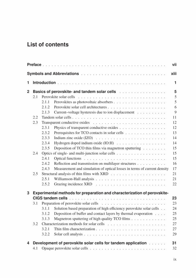
List of contents
Preface . . . . . . . . . . . . . . . . . . . . . . . . . . . . . . . . . . . . . . . . . . vii
Symbols and Abbreviations . . . . . . . . . . . . . . . . . . . . . . . . . . . . . xiii
1 Introduction . . . . . . . . . . . . . . . . . . . . . . . . . . . . . . . . . . . . . 1
2 Basics of perovskite- and tandem solar cells . . . . . . . . . . . . . . . . 52.1 Perovskite solar cells . . . . . . . . . . . . . . . . . . . . . . . . . . . . . . 5
2.1.1 Perovskites as photovoltaic absorbers . . . . . . . . . . . . . . . . . . 52.1.2 Perovskite solar cell architectures . . . . . . . . . . . . . . . . . . . . 62.1.3 Current–voltage hysteresis due to ion displacement . . . . . . . . . . 9
2.2 Tandem solar cells . . . . . . . . . . . . . . . . . . . . . . . . . . . . . . . . 112.3 Transparent conductive oxides . . . . . . . . . . . . . . . . . . . . . . . . . 12
2.3.1 Physics of transparent conductive oxides . . . . . . . . . . . . . . . . 122.3.2 Prerequisites for TCO contacts in solar cells . . . . . . . . . . . . . . 132.3.3 Indium zinc oxide (IZO) . . . . . . . . . . . . . . . . . . . . . . . . 142.3.4 Hydrogen doped indium oxide (IO:H) . . . . . . . . . . . . . . . . . 142.3.5 Deposition of TCO thin films via magnetron sputtering . . . . . . . . 15
2.4 Optics of single- and multi-junction solar cells . . . . . . . . . . . . . . . . . 152.4.1 Optical functions . . . . . . . . . . . . . . . . . . . . . . . . . . . . 152.4.2 Reflection and transmission on multilayer structures . . . . . . . . . . 162.4.3 Measurement and simulation of optical losses in terms of current density 17
2.5 Structural analysis of thin films with XRD . . . . . . . . . . . . . . . . . . . 212.5.1 Williamson-Hall analysis . . . . . . . . . . . . . . . . . . . . . . . . 212.5.2 Grazing incidence XRD . . . . . . . . . . . . . . . . . . . . . . . . 22
3 Experimental methods for preparation and characterization of perovskite-CIGS tandem cells . . . . . . . . . . . . . . . . . . . . . . . . . . . . . . . . . 233.1 Preparation of perovskite solar cells . . . . . . . . . . . . . . . . . . . . . . 23
3.1.1 Solution based preparation of high efficiency perovskite solar cells . . 243.1.2 Deposition of buffer and contact layers by thermal evaporation . . . . 253.1.3 Magnetron sputtering of high quality TCO films . . . . . . . . . . . . 25
3.2 Characterization methods for solar cells . . . . . . . . . . . . . . . . . . . . 273.2.1 Thin film characterization . . . . . . . . . . . . . . . . . . . . . . . . 273.2.2 Solar cell analysis . . . . . . . . . . . . . . . . . . . . . . . . . . . . 29
4 Development of perovskite solar cells for tandem application . . . . . . 314.1 Opaque perovskite solar cells . . . . . . . . . . . . . . . . . . . . . . . . . . 32
ix

List of contents
4.1.1 Principle investigations on MAPI based solar cells . . . . . . . . . . . 334.1.2 Nanoparticles for efficient wetting on hydrophobic fullerene interfaces 354.1.3 Increased efficiency and reduced hysteresis with fullerene interlayers . 41
4.2 Sputter-deposition of suitable transparent conductive oxides as transparent elec-trodes . . . . . . . . . . . . . . . . . . . . . . . . . . . . . . . . . . . . . . 444.2.1 Amorphous indium zinc oxide deposited with low thermal impact . . 454.2.2 Hydrogen doped indium oxide with ultra-low absorption . . . . . . . 474.2.3 Comparison between optimized IZO and IO:H layers and commercial
available TCO substrates . . . . . . . . . . . . . . . . . . . . . . . . 574.3 Semitransparent perovskite solar cells . . . . . . . . . . . . . . . . . . . . . 59
4.3.1 Sputter deposition of transparent rear electrodes with protective layersagainst damages . . . . . . . . . . . . . . . . . . . . . . . . . . . . . 60
4.3.2 Implementation of IZO and PDC-IO:H as front electrodes with ultra-lowNIR absorption . . . . . . . . . . . . . . . . . . . . . . . . . . . . . 66
4.3.3 The optical influence of TCO layer thickness . . . . . . . . . . . . . 69
5 Four-terminal perovskite–CIGS tandem cells . . . . . . . . . . . . . . . . . 755.1 Design and performance aspects of four-terminal tandem architectures . . . . 76
5.1.1 Optical mismatch between perovskite solar cells and representative filterdevices . . . . . . . . . . . . . . . . . . . . . . . . . . . . . . . . . 77
5.1.2 Reducing the series resistance of the perovskite solar cell by implemen-tation of a metal grid . . . . . . . . . . . . . . . . . . . . . . . . . . 79
5.2 Investigation of suitable CIGS bottom cells . . . . . . . . . . . . . . . . . . . 875.2.1 CIGS architectures with different band gaps . . . . . . . . . . . . . . 875.2.2 CIGS bottom cell performance estimations from single diode models . 905.2.3 Estimation of the CIGS performance under different illumination con-
ditions . . . . . . . . . . . . . . . . . . . . . . . . . . . . . . . . . . 935.3 Photovoltaic performance of tandem architectures with different perovskite and
TCO combinations . . . . . . . . . . . . . . . . . . . . . . . . . . . . . . . 965.3.1 Simple perovskite based top cells . . . . . . . . . . . . . . . . . . . . 965.3.2 Multi cation perovskite based top cells . . . . . . . . . . . . . . . . . 98
5.4 Potential for further optimizations of perovskite–CIGS tandem solar cells . . 1055.4.1 Simulation assisted analysis of the parasitic losses . . . . . . . . . . . 1055.4.2 Improvement of the light management by using immersion oil for optical
coupling and anti-reflective foil . . . . . . . . . . . . . . . . . . . . . 1105.4.3 Increasing the CIGS efficiency by implementing wide band gap top cells
with higher transmission . . . . . . . . . . . . . . . . . . . . . . . . 115
6 Summary . . . . . . . . . . . . . . . . . . . . . . . . . . . . . . . . . . . . . . 119
A Appendix . . . . . . . . . . . . . . . . . . . . . . . . . . . . . . . . . . . . . . 123A.1 Ellipsometry models . . . . . . . . . . . . . . . . . . . . . . . . . . . . . . 123A.2 Quantum efficiency measurements . . . . . . . . . . . . . . . . . . . . . . . 126
Bibliography . . . . . . . . . . . . . . . . . . . . . . . . . . . . . . . . . . . . . . 129
x

List of contents
Author’s Publications . . . . . . . . . . . . . . . . . . . . . . . . . . . . . . . . . 139Journal Papers . . . . . . . . . . . . . . . . . . . . . . . . . . . . . . . . . . . . . 139Conference Contributions . . . . . . . . . . . . . . . . . . . . . . . . . . . . . . . 139
xi

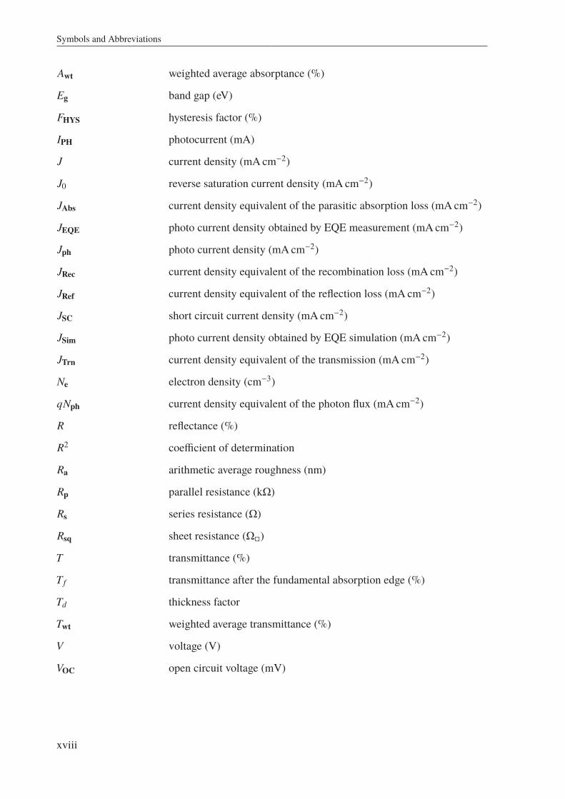
Symbols and Abbreviations
Abbreviations
2T two-terminal
4P four-point-probe
4T four-terminal
a-IO:H amorphous hydrogenated indium oxide
Al2O3-NP aluminium oxide nanoparticle
AM1.5 AM1.5G solar spectrum
Ar argon
ARF anti reflection foil
ARC anti reflection coating
BCP conductive copper complex(2,9-Dimethyl-4,7-diphenyl-1,10-phenanthroline (bathocuproine))
C60–SAM C60-based self-assembled monolayer(4-(1’,5’-Dihydro-1’methyl-2’H-[5,6]fullereno-C60-Ih-[1,9-c]pyrrol-2’-yl)benzoic acid)
CB chlorobenzene
CdS cadmium sulfide
CIGS copper indium gallium diselenide (CuInxGa1– xSe2)
CIGSa CIGS cell with Eg = 1.1 eV
CIGSb CIGS cell with Eg = 1.0 eV
CLSM confocal laser scanning microscopy
CsI caesium iodide
CsFAMAPIBr mixed ionic perovskite (Cs0.05(FA0.83MA0.17)0.95Pb(I0.83Br0.17)3)
c-SnO2 compact tin oxide
c-TiO2 compact titanium oxide
DC direct current
xiii

Symbols and Abbreviations
DCB dichlorobenzene
DMF dimethylformamide
DMSO dimethylsulfoxide
EBPVD electron-beam physical vapor deposition
EDOT-Amide-TPA conductive amide(N5,N7-bis(4-(bis(4-methoxyphenyl)amino)phenyl)-2,3-dihydrothieno[3,4-b][1,4]dioxine-5,7-dicarboxamide)
ETL electron transport layer
EQE external quantum efficiency
FA+ formamidinium ((NH2 –CH––NH2)+)
FAI formamidinium iodide
FCA free carrier absorption
FF fill factor
FIB focused ion beam
FTO fluorine doped tin oxide
fwd forward
FWHM full width at half maximum
FWHMinst instrumental diffraction peak broadening
FWHMstruct structural diffraction peak broadening
GBL γ–butyrolactone
GDOES glow discharge optical emission spectroscopy
GGI gallium to indium ratio ([Ga]/([Ga] + [In]))
GIXRD grazing incidence x-ray diffraction
H2 hydrogen
H2O water
HTL hole transport layer
i-ZnO intrinsic zinc oxide
IV current–voltage dependency
IMEC Interuniversity Microelectronics Centre
In2O3 indium oxide
IO:H hydrogen-doped indium oxide
xiv

Symbols and Abbreviations
IOOH indium oxide hydroxide
IPA isopropanol
ITO indium tin oxide
IZO indium zinc oxide ((In2O3)0.9(ZnO)0.1)
JV current-density–voltage dependency
KIT Karlsruher Institut für Technologie
LMU Ludwig-Maximilian-Universität München
MA+ methylammonium ((CH3 –NH3)+)
MABr methylammonium bromide
MAI methylammonium iodide
MAPI MAPbI3
MgF2 magnesium fluoride
Mo molybdenum
MoO3 molybdenum oxide
MPP maximum power point
n-i-p n-type–intrinsic–p-type
NIR near-infrared
NP nanoparticle
O2 oxygen
PCBM C61 fullerene derivate ([6,6]-phenyl-C61-butyric acid methyl ester)
PCE power conversion efficiency at standard test conditions
PCEf power conversion efficiency under a filtered AM1.5G spectrum
PCEMPP power conversion efficiency at steady state conditions
PCESim power conversion efficiency obtained from single diode modelsimulation
PDC post-deposition-crystallisation
PDC–IO:H post-deposition-crystallised hydrogenated indium oxide
PbBr2 lead bromide
PbI2 lead iodide
PET polyethylene terephthalate
xv
Symbols and Abbreviations
p-i-n p-type–intrinsic–n-type
PMMA poly(methyl methacrylate)
PSC perovskite solar cell
PSCa perovskite solar cell with PDC-IO:H front electrode
PSCb perovskite solar cell with ITO front electrode
PTAA conductive polyamine(poly[bis(4-phenyl)(2,4,6-trimethylphenyl)amine])
PV photovoltaic
PVD physical vapor deposition
RbCsFAPbIBr wide band gap perovskite (Rb0.05Cs0.17FA0.78Pb(I0.60Br0.40)3)
RF radio frequency
rvs reverse
RMS root mean square
SC spin coating
SCAPS SCAPS simulation software
SE spectroscopic ellipsometry
SEM scanning electron microscopy
SiO2 silicon oxide
SiO2-NP silicon oxide nanoparticle
SnO2 tin oxide
SnO2-NP tin oxide nanoparticle
Spiro-OMeTAD conductive fluorene(2,2’,7,7’-Tetrakis[N,N-di(4-methoxyphenyl)amino]-9,9’-spirobifluorene)
STEM scanning transmission electron microscopy
TCO transparent conductive oxide
TiO2 titanium oxide
TLD through-lens-detector
TMM transfer matrix method
UHV ultra high vacuum
UV ultra violet
xvi

Symbols and Abbreviations
UV/Vis ultra violet to visible
WBG wide band gap
XRD x-ray diffraction
XRR x-ray reflectometry
ZAO aluminium doped zinc oxide ZnxAl1– xO
ZMO zinc magnesium oxide ZnxMg1– xO
ZSW Zentrum für Sonnenenergie- und Wasserstoff-ForschungBaden-Württemberg
Constants
π Circle constant (3,14159 . . .)
h Planck constant (6.626 070 15 × 10−34 J s)
k Boltzmann constant (1.380 649 × 10−23 J K−1)
m0 electron resting mass (9.109 383 701 5 × 10⁻³¹ kg)
q elementary charge (1.602 176 634 × 10−34 C)
Latin Variables
Minuscule
d film thickness (nm)
frot rotational frequency (s−1)
hν photon energy (eV)
k(λ) imaginary part of the complex refractive index or extinction coefficient
m∗e effective electron mass
N complex refractive index
n diode ideality factor
n(λ) real part of the complex refractive index or phase velocity
Capital
A absorptance (%)
Aact active area (cm2)
xvii
Symbols and Abbreviations
Awt weighted average absorptance (%)
Eg band gap (eV)
FHYS hysteresis factor (%)
IPH photocurrent (mA)
J current density (mA cm−2)
J0 reverse saturation current density (mA cm−2)
JAbs current density equivalent of the parasitic absorption loss (mA cm−2)
JEQE photo current density obtained by EQE measurement (mA cm−2)
Jph photo current density (mA cm−2)
JRec current density equivalent of the recombination loss (mA cm−2)
JRef current density equivalent of the reflection loss (mA cm−2)
JSC short circuit current density (mA cm−2)
JSim photo current density obtained by EQE simulation (mA cm−2)
JTrn current density equivalent of the transmission (mA cm−2)
Ne electron density (cm−3)
qNph current density equivalent of the photon flux (mA cm−2)
R reflectance (%)
R2 coefficient of determination
Ra arithmetic average roughness (nm)
Rp parallel resistance (kΩ)
Rs series resistance (Ω)
Rsq sheet resistance (Ω)
T transmittance (%)
T f transmittance after the fundamental absorption edge (%)
Td thickness factor
Twt weighted average transmittance (%)
V voltage (V)
VOC open circuit voltage (mV)
xviii

Symbols and Abbreviations
Greek Variables
α absorption coefficient (cm−1)
λ wavelength (nm)
ε microstrain (%)
εwt weighted microstrain (%)
µ charge carrier mobility (cm2 V−1s−1)
µatt linear attenuation coefficient (cm−1)
τ penetration depth (nm)
τ relaxation time (s)
ω incident angle (°)
ωc critical angle (°)
ρ resistivity (Ω cm)
2θ diffracted angle (°)
xix

1 Introduction
Photovoltaics play a central role in the transition from fossil to renewable energy. The sun isthe most significant source of energy that provides a constant supply to planet earth. In orderto exploit solar energy, more efficient and cost-effective photovoltaic (PV) devices are required.Additionally, new PV technologies are desired that provide more versatile functionalities e.g.for building integration, mobile applications, curved surfaces, or individual shapes, colours andform factors.
In contrast to silicon PV technology, two thin-film technologies with a certificated power conver-sion efficiency (PCE) above 23 % could allow cost-effective, lightweight and potentially flexibleall-thin-film devices to meet the new demands of the future: perovskite solar cells (PSCs) andcopper indium gallium diselenide (CIGS) solar cells. Their power conversion efficiency can sur-pass the single-junction Shockley-Queisser limit [1], by combining the two thin-film materialstogether in a tandem configuration [2].
Perovskite solar cells are especially suitable for use in tandem cells, stacked on top of a CIGSbottom cell, because their band gap is naturally quite wide. Consequently, the absorption rangeof thematerial is restricted to the higher energetic wavelengths and a large fraction of the sunlighttransmits to the CIGS tandem partner. Moreover, the band gaps of both thin-film materials areeasily tunable by variations of the composition, which allows engineering the absorption rangesof both subcells in order to achieve maximum power output. The wide band gaps of efficientPSCs can be adjusted in between 1.6 eV to 1.8 eV [3], while the band gap of CIGS can benarrowed down to ≈1.0 eV [4, 5] to maximize the absorption range.
Highly efficient perovskite–CIGS tandem cells have already been reported for mechanicallystacked, four-terminal (4T) architectures (25.9 %) [6] or monolithic, two-terminal (2T) architec-tures (22.4 %) [7], demonstrating their great potential.
Although it is an ongoing debate whether the 4T or 2T architecture will be the most efficient,cost-effective and reliable solution in the future [8–12], these tandem architectures share a jointrestriction: They are limited in their efficiency by parasitic near-infrared (NIR) absorption withinthe perovskite top cell. It ideally collects all light within its absorption range, typically up to700 nm or 800 nm, while the CIGS bottom cell uses the transmitted near-infrared (NIR) light.Hence, any parasitic absorption in the layers of the top cell leads to a direct decline of the powergenerated by the bottom cell. The electrodes of the top cell often cause the largest contributionto the NIR absorption.
Reducing the parasitic absorption in the transparent electrodes ismost challenging since they haveto be both an electrical conductor and optical transmitter. Commercial transparent conductiveoxides (TCOs) such as fluorine doped tin oxide (FTO) or indium tin oxide (ITO) are prominentlyused for single-junction perovskite cells. Given their high free carrier density, they have excellentconductivity, but also high free carrier absorption in NIR, which makes them unfavourable fortandem solar cells.
1
1 Introduction
Advanced TCOs such as hydrogen-doped indium oxide (IO:H) and indium zinc oxide (IZO)provide the possibility to achieve a much lower NIR absorption due to their low charge carrierdensity, which is compensated by their exceptionally high electron mobility that simultaneouslyallows for high conductivity. Especially annealed IO:H promises suitable properties with areported charge carrier density range from 1.1 × 1020 cm−3 to 2.1 × 1020 cm−3 and a chargecarrier mobility range from 80 cm2 V−1s−1 to 140 cm2 V−1s−1 [13–16]. Although these TCOshave already been reported in previous perovskite-based tandem architectures [2, 17, 18], thisresearch aims to develop a more detailed understanding of the parasitic absorption mechanismsin semitransparent PSCs and the complete tandem setup.
Compared to single-junction devices, the evaluation of the losses becomes increasingly difficultin tandem solar cells because of the high number of layers. Computed simulations are needed todetermine the parasitic absorption of each layer, but the simulation itself requires precise inputdata from supplementary measurements to generate a correct model of the optical propertiesof the complete architecture. Such modelling capabilities are the basis for a systematic futuredevelopment of tandem cells.
An additional concern regarding the development of tandem cells is that previous studies oftenestimated the 4T tandem efficiency by adding the efficiency values of small-area semitransparentperovskite cells on ≈0.1 cm2 with those of larger bottom cells >0.5 cm2. In that case, the CIGSbottom cell is covered by a filter that shall represent the optical response of a large-area perovskitetop solar cell [2,19,20]. However, this is a very idealized scenario that disregards realistic lossesfrom which the tandem setup would suffer when the PSC area is large enough to match thebottom cell size. On the one hand, the power conversion efficiency of the PSC would bereduced, mainly because of the lateral conductive resistance of the TCO electrodes, but also dueto the challenges to produce high-quality devices on a larger area with the usual solution-baseddeposition techniques. On the other hand, metal grids would likely be implemented to improvecurrent transport in the electrodes — a standard for other solar cell technologies. A grid causesan additional shadow cast on the bottom cell leading to a reduced current generation, an effectwhich is not accounted for in a filter-based estimation.
In order to overcome the above-mentioned challenges, the tasks of this dissertation formulate asfollows:
• Development of efficient PSCs
• Optimization of highly transparent IO:H and IZO electrodes
• Implementation of the transparent electrodes into PSCs
• Increasing the cell size of the PSC to 0.5 cm2
• Fabrication of 4T tandem cells with matching cell sizes and integrated metal grids
• Modelling and analysis of the loss mechanisms in tandem cells
2
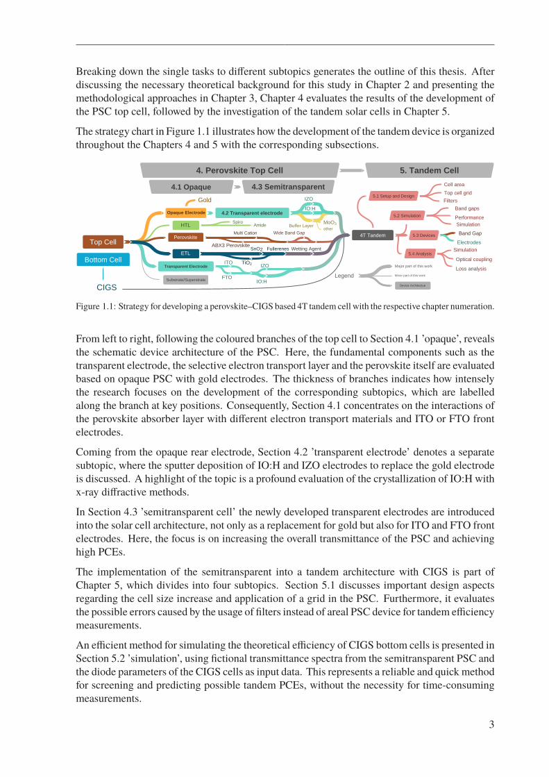
Breaking down the single tasks to different subtopics generates the outline of this thesis. Afterdiscussing the necessary theoretical background for this study in Chapter 2 and presenting themethodological approaches in Chapter 3, Chapter 4 evaluates the results of the development ofthe PSC top cell, followed by the investigation of the tandem solar cells in Chapter 5.
The strategy chart in Figure 1.1 illustrates how the development of the tandem device is organizedthroughout the Chapters 4 and 5 with the corresponding subsections.
4.1 Opaque 4.3 Semitransparent
4. Perovskite Top Cell 5. Tandem Cell
Bottom Cell
CIGS
Top Cell
LegendDevice Architectue
Minor part of this work
Major part of this work
Substrate/Superstrate
Transparent ElectrodeITO
IO:H
IZO
FTO
Opaque Electrode
Gold
4.2 Transparent electrodeIO:H
otherMoO3
IZO
HTL Spiro
Perovskite
Amide
Multi Cation
ABX3 PerovskiteETL
TiO2
SnO2 Fullerenes Wetting Agent
4T Tandem 5.3 Devices
Buffer Layer Wide Band Gap
5.1 Setup and DesignFilters
5.4 Analysis
Top cell grid
Cell area
5.2 Simulation
Simulation
Band Gap
Electrodes
Simulation
Band gaps
Performance
Optical coupling
Loss analysis
Figure 1.1: Strategy for developing a perovskite–CIGS based 4T tandem cell with the respective chapter numeration.
From left to right, following the coloured branches of the top cell to Section 4.1 ’opaque’, revealsthe schematic device architecture of the PSC. Here, the fundamental components such as thetransparent electrode, the selective electron transport layer and the perovskite itself are evaluatedbased on opaque PSC with gold electrodes. The thickness of branches indicates how intenselythe research focuses on the development of the corresponding subtopics, which are labelledalong the branch at key positions. Consequently, Section 4.1 concentrates on the interactions ofthe perovskite absorber layer with different electron transport materials and ITO or FTO frontelectrodes.
Coming from the opaque rear electrode, Section 4.2 ’transparent electrode’ denotes a separatesubtopic, where the sputter deposition of IO:H and IZO electrodes to replace the gold electrodeis discussed. A highlight of the topic is a profound evaluation of the crystallization of IO:H withx-ray diffractive methods.
In Section 4.3 ’semitransparent cell’ the newly developed transparent electrodes are introducedinto the solar cell architecture, not only as a replacement for gold but also for ITO and FTO frontelectrodes. Here, the focus is on increasing the overall transmittance of the PSC and achievinghigh PCEs.
The implementation of the semitransparent into a tandem architecture with CIGS is part ofChapter 5, which divides into four subtopics. Section 5.1 discusses important design aspectsregarding the cell size increase and application of a grid in the PSC. Furthermore, it evaluatesthe possible errors caused by the usage of filters instead of areal PSC device for tandem efficiencymeasurements.
An efficient method for simulating the theoretical efficiency of CIGS bottom cells is presented inSection 5.2 ’simulation’, using fictional transmittance spectra from the semitransparent PSC andthe diode parameters of the CIGS cells as input data. This represents a reliable and quick methodfor screening and predicting possible tandem PCEs, without the necessity for time-consumingmeasurements.
3

1 Introduction
Section 5.3 ’devices’ evaluates the performance of actual tandem setups comprising differentPSC top cells and CIGS bottom cells. As a highlight, a champion tandem cell with 23.0 % PCEon 0.5 cm2 is presented.
The optical and electronic properties of the tandem cells are investigated with a detailed currentloss analysis in the last Section 5.4 ’analysis’. The analysis follows a transfer matrix method(TMM) approach in which an optical model comprising all optical functions of the individuallayers of the architecture is created, in order to track the loss mechanisms of the tandem cell.This method demonstrates how large the impact of the new highly transmissive IO:H andIZO electrodes is compared to a standard electrode like conventional ITO. Furthermore, thefindings address the most relevant remaining losses in the other layers, which can be targeted infuture development steps. Following the discussion for further improvements, the applicationof immersion oil as an optical coupling material between the PSC and the CIGS cell is tested,and the impact of PSC top cells with an optimized, higher band gap and close-to-perfect NIRtransmission is estimated.
Chapter 6 concludes this dissertation with a summarizing of the most relevant results.
4

2 Basics of perovskite- and tandem solar cells
This chapter gives an overview on the specific theories and recent progress in research relatedto the topics that are of concern for this thesis. After introducing perovskites as photovoltaicabsorbers and discussing their relevant features and challenges in Section 2.1, a brief introduc-tion on tandem solar cells is given in Section 2.2, focusing on 4T perovskite–CIGS tandems.Subsequently, Section 2.3 introduces the relevant aspects of the functionality and deposition ofTCOs, specifically IO:H and IZO. Section 2.4 refers to the special optical properties of themultilayer structures of tandem solar cells and Section 2.5 is dedicated to specified features ofx-ray diffraction (XRD) for strain analysis in thin films.
2.1 Perovskite solar cells
The following sections explain, why the perovskite material is a highly promising absorbermaterial for PV, introduce the architectural concept of PSCs and evaluate reasons for theoccurrence of current-voltage hysteresis.
2.1.1 Perovskites as photovoltaic absorbers
Originally, Gustav Rose gave the name ’Perovskite’ to the novel mineral calcium titanate(CaTiO3) in the year 1839, honouring the Russian mineralogist Lev Perovski [21]. Sincethen, the nomenclature has been used for materials that exhibit the same crystal structure ABX3.
The organic-inorganic perovskite material, that is of interest in this study, first emerged in1978 [22] and the first perovskite solar cell was published in 2009 [23].
The cubic structure of ABX3 perovskite is shown in Figure 2.1, but depending on the tilt of thecentral octahedron, the crystal may exhibit a lower orthorhombic or tetragonal symmetry. Thisreversible phase change depends on external parameters such as temperature and pressure, butalso on the ionic radii of the compounds.
Figure 2.1: ABX3 perovskite structure with possible ions for each side, adapted from Powalla et al. [24]
5

2 Basics of perovskite- and tandem solar cells
The most commonly used compounds for photovoltaic applications are methylammonium(MA+)1 at site A, lead (Pb2+) at site B and iodine (I– ) at site X, resulting in the final for-mulation of MAPbI3 (MAPI) with reported band gaps around 1.55 to 1.6 eV [24]. The basicfeatures that make MAPI a good absorber material for photovoltaic application are
• a high absorption coefficient over 1.5 × 104 cm−1 [25],
• a low exciton binding energy below 30 meV [141] [26, 27],
• high diffusion lengths over 1 µm [28, 29],
• long carrier lifetimes over 1 µs [30],
• and high carrier mobilities of 10 to 40 cm2 V−1s−1 [31].
A partial replacement of the ions opens up a wide field of mixed ion perovskites, which bringsseveral advantages. On one hand, the band gap of the material is easily tunable with thereplacement of the X site cation (e.g. with Sn2+) or the B site anion (e.g. Br– or Cl– ) or theA site (e.g. formamidinium (FA+)2, Cs+ or Rb+), which makes the perovskites fascinating fortandem application. On the other hand, an increased level of mixing different anions and cationsproved beneficial effects on the stability, reproducibility and overall efficiency of the perovskitematerial. [32] This study comprises the simple MAPI approach, as well as the prominent mixedionic perovskite (CsFAMAPIBr)3, as introduced by Saliba et al. [33].
2.1.2 Perovskite solar cell architectures
The principle setup of a planar perovskite solar cell, how it is used in this study, consists of theperovskite absorber itself, a hole transport layer (HTL) and an electron transport layer (ETL) forcharge carrier separation and contact layers for charge carrier extraction. Figure 2.2 demonstratesthe working principle of the solar cell with selective contacts as proposed by Peter Würfel [34].
Absorber p-typen-type
0
ε
εf,left
εf,right
εv
εc
εf,c εf,v
-
+
x
Figure 2.2: Illustration after Würfel [34] showing a setup for extraction of electrons and holes with the use of n-typeand p-type selective membranes (ETL and HTL). Because of the barriers introduced by the selectivelayers, the charges are effectively separated to the different contacts on both sides.
1 (CH3 –NH3)+2 (NH2 –CH––NH2)+3 Cs0.5(FA0.83MA0.17)0.95Pb(I0.83Br0.17)3
6
2.1 Perovskite solar cells
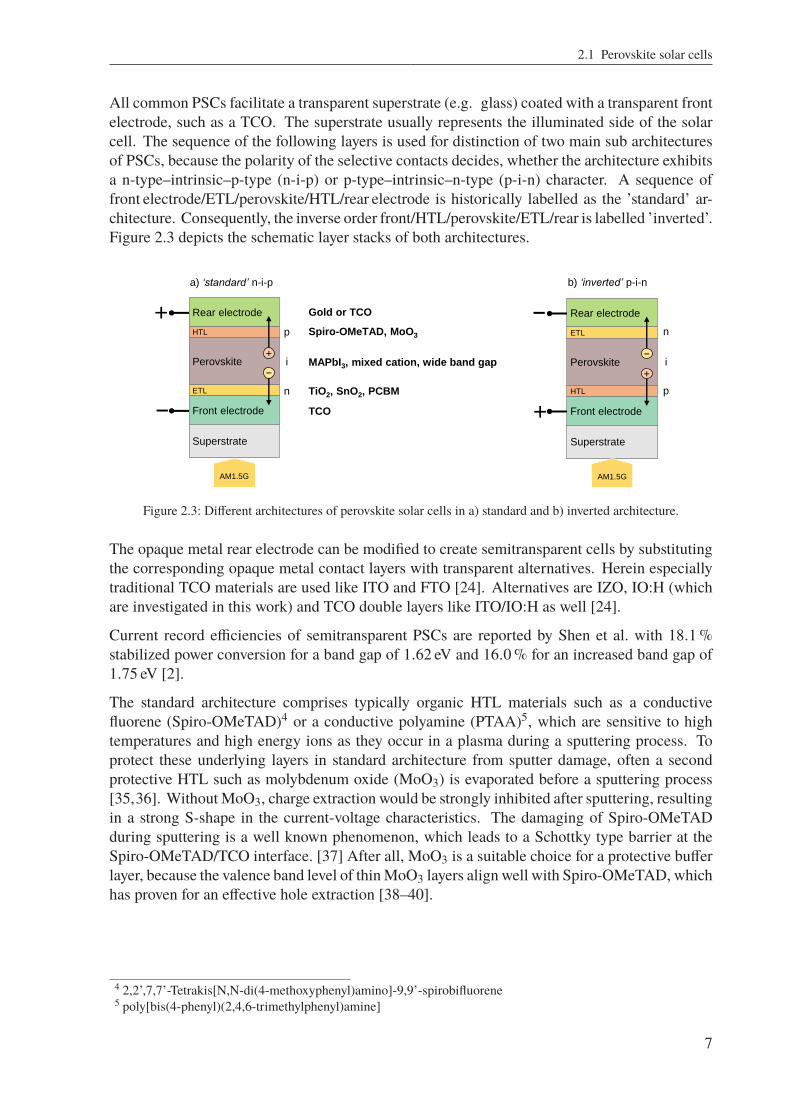
All common PSCs facilitate a transparent superstrate (e.g. glass) coated with a transparent frontelectrode, such as a TCO. The superstrate usually represents the illuminated side of the solarcell. The sequence of the following layers is used for distinction of two main sub architecturesof PSCs, because the polarity of the selective contacts decides, whether the architecture exhibitsa n-type–intrinsic–p-type (n-i-p) or p-type–intrinsic–n-type (p-i-n) character. A sequence offront electrode/ETL/perovskite/HTL/rear electrode is historically labelled as the ’standard’ ar-chitecture. Consequently, the inverse order front/HTL/perovskite/ETL/rear is labelled ’inverted’.Figure 2.3 depicts the schematic layer stacks of both architectures.
a) ‘standard’ n-i-p
Superstrate
HTL
Perovskite
ETL
Rear electrode
Front electrode
+
−
−
+
b) ‘inverted’ p-i-n
Superstrate
ETL
Perovskite
HTL
Rear electrode
Front electrode
−
+
+
−
p
n p
n
Gold or TCO
Spiro-OMeTAD, MoO3
MAPbI3, mixed cation, wide band gap
TiO2, SnO2, PCBM
TCO
i i
AM1.5G AM1.5G
Figure 2.3: Different architectures of perovskite solar cells in a) standard and b) inverted architecture.
The opaque metal rear electrode can be modified to create semitransparent cells by substitutingthe corresponding opaque metal contact layers with transparent alternatives. Herein especiallytraditional TCO materials are used like ITO and FTO [24]. Alternatives are IZO, IO:H (whichare investigated in this work) and TCO double layers like ITO/IO:H as well [24].
Current record efficiencies of semitransparent PSCs are reported by Shen et al. with 18.1 %stabilized power conversion for a band gap of 1.62 eV and 16.0 % for an increased band gap of1.75 eV [2].
The standard architecture comprises typically organic HTL materials such as a conductivefluorene (Spiro-OMeTAD)4 or a conductive polyamine (PTAA)5, which are sensitive to hightemperatures and high energy ions as they occur in a plasma during a sputtering process. Toprotect these underlying layers in standard architecture from sputter damage, often a secondprotective HTL such as molybdenum oxide (MoO3) is evaporated before a sputtering process[35,36]. Without MoO3, charge extraction would be strongly inhibited after sputtering, resultingin a strong S-shape in the current-voltage characteristics. The damaging of Spiro-OMeTADduring sputtering is a well known phenomenon, which leads to a Schottky type barrier at theSpiro-OMeTAD/TCO interface. [37] After all, MoO3 is a suitable choice for a protective bufferlayer, because the valence band level of thinMoO3 layers align well with Spiro-OMeTAD, whichhas proven for an effective hole extraction [38–40].
4 2,2’,7,7’-Tetrakis[N,N-di(4-methoxyphenyl)amino]-9,9’-spirobifluorene5 poly[bis(4-phenyl)(2,4,6-trimethylphenyl)amine]
7
2 Basics of perovskite- and tandem solar cells
For inverted architecture common used ETL materials on top of the cell stack are for examplea combination of a C61 fullerene derivate (PCBM)6 and a conductive copper complex (BCP)7,where damage can be healed by annealing [144].
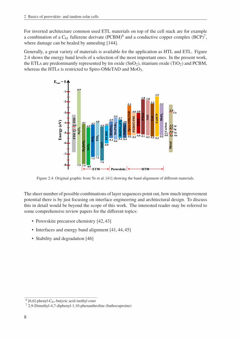
Generally, a great variety of materials is available for the application as HTL and ETL. Figure2.4 shows the energy band levels of a selection of the most important ones. In the present work,the ETLs are predominantly represented by tin oxide (SnO2), titanium oxide (TiO2) and PCBM,whereas the HTLs is restricted to Spiro-OMeTAD and MoO3.
Figure 2.4: Original graphic from Ye et al. [41] showing the band alignment of different materials.
The sheer number of possible combinations of layer sequences point out, howmuch improvementpotential there is by just focusing on interface engineering and architectural design. To discussthis in detail would be beyond the scope of this work. The interested reader may be referred tosome comprehensive review papers for the different topics:
• Perovskite precursor chemistry [42, 43]
• Interfaces and energy band alignment [41, 44, 45]
• Stability and degradation [46]
6 [6,6]-phenyl-C61-butyric acid methyl ester7 2,9-Dimethyl-4,7-diphenyl-1,10-phenanthroline (bathocuproine)
8

2.1 Perovskite solar cells
2.1.3 Current–voltage hysteresis due to ion displacement
Already in early stages of the development of PSCs researchers noticed something peculiarabout the devices: The current-density–voltage dependency (JV) scans show different responsesdepending on the sweep direction, scan speed and light biasing [47–49]. Figure 2.5 shows tworepresentative examples of the hysteresis observed in this study. The main difference betweenthe JV curves originating from the forward (fwd) scan and the reverse (rvs) scan is observed inthe fill factor (FF) as demonstrated in Figure 2.5a, but also the open circuit voltage (VOC) maybe affected as shown in b.
0.0 0.4 0.8 1.2
-20
-15
-10
-5
0
5
J (
mA
cm
-2)
V (V)0.0 0.4 0.8 1.2
-20
-15
-10
-5
0
5
J (
mA
cm
-2)
V (V)
rvs fwd
PCE (%) 15.8 9.8
FF (%) 73.6 60.0
VOC (mV) 1136 866
JSC (mA cm-2) 18.8 18.9
FHYS (%) 38.0
rvs fwd
PCE (%) 12.0 4.5
FF (%) 62.3 23.6
VOC (mV) 1070 1059
JSC (mA cm-2) 18.0 17.8
FHYS (%) 62.2
a) b)
Figure 2.5: Representative examples of JV responses of two PSCs that exhibit strong hysteresis between the forwardand reverse scan direction as indicated by arrows. In a) the hysteresis mainly affects the FF, whereas inb) FF and VOC are affected.
Since the discovery, there is a continuing tremendous effort to understand the origin of thehysteresis. A broad consensus claims that the hysteresis is mainly the result of mobile ions andtheir vacancies in the perovskite structure. Several review papers have been published over thelast years, giving a very detailed insight over the different approaches to study and overcome thehysteresis [50–52].
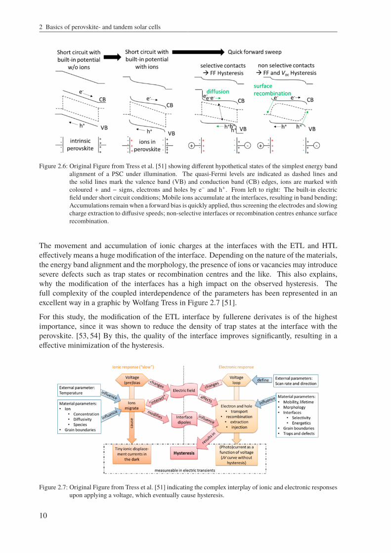
Figure 2.6 explains schematically how mobile ions in the perovskite accumulate at the interfacesand hinder the charge extraction and injection by screening the contact potential in a fast fwdscan.
9
2 Basics of perovskite- and tandem solar cells
Figure 2.6: Original Figure from Tress et al. [51] showing different hypothetical states of the simplest energy bandalignment of a PSC under illumination. The quasi-Fermi levels are indicated as dashed lines andthe solid lines mark the valence band (VB) and conduction band (CB) edges, ions are marked withcoloured + and − signs, electrons and holes by e− and h+. From left to right: The built-in electricfield under short circuit conditions; Mobile ions accumulate at the interfaces, resulting in band bending;Accumulations remain when a forward bias is quickly applied, thus screening the electrodes and slowingcharge extraction to diffusive speeds; non-selective interfaces or recombination centres enhance surfacerecombination.
The movement and accumulation of ionic charges at the interfaces with the ETL and HTLeffectively means a huge modification of the interface. Depending on the nature of the materials,the energy band alignment and the morphology, the presence of ions or vacancies may introducesevere defects such as trap states or recombination centres and the like. This also explains,why the modification of the interfaces has a high impact on the observed hysteresis. Thefull complexity of the coupled interdependence of the parameters has been represented in anexcellent way in a graphic by Wolfang Tress in Figure 2.7 [51].
For this study, the modification of the ETL interface by fullerene derivates is of the highestimportance, since it was shown to reduce the density of trap states at the interface with theperovskite. [53, 54] By this, the quality of the interface improves significantly, resulting in aeffective minimization of the hysteresis.
Figure 2.7: Original Figure from Tress et al. [51] indicating the complex interplay of ionic and electronic responsesupon applying a voltage, which eventually cause hysteresis.
10

2.2 Tandem solar cells
In order to quantify the hysteresis or in other words the discrepancy between fwd and rvs scan,a hysteresis factor (FHYS) is introduced as following
FHYS =PCErvs − PCE f wd
PCErvs(2.1)
with the PCE extracted from both scan directions, respectively. Compare also Section 3.2.2
Using the FHYS, the hysteresis behaviour of different samples can be compared, under theprecondition that they have been measured in the same manner. Since the measured PCE of theJV scan is dependent on a whole set of measurement parameters, such as scan direction, scanspeed, measurement delay, pre biasing, light soaking, and even environmental conditions, theabsolute PCE value of neither fwd nor rvs scan has a real quantitative meaning. [50]
A much more reliable measure of the PCE is a smart, iterative maximum power point (MPP)tracking under illumination in order to record the steady state power output from the device.From this measurement, the power conversion efficiency at steady state conditions (PCEMPP)is received. In devices with a large hysteresis the steady state condition might be reached onlyafter several tens of seconds, indicating itself a bad quality of the interface. If the device reachesthe steady state condition quickly, and shows a stable power output, a close agreement of theMPP efficiency and the JV-based PCE value would be a strong indicator for a good interface.
2.2 Tandem solar cells
The principle of a tandem cell is the combination of a high band gap top cell with a low bandgap bottom cell which absorb different parts of the solar spectrum. It is possible to classifytandem solar cells as two- or four-terminal (2T and 4T, respectively) devices. Figure 2.8 showsan example with a perovskite top cell and a CIGS bottom cell.
a) Four terminal tandem architectures b) Two terminal tandem architecture
Front electrode
CIGS
Mo
Superstrate
Perovskite
Rear electrode
Front electrode−
+
+
−
AM1.5G
NIR
+
Front electrode
CIGS
Mo
Superstrate
Perovskite
Rear electrode
Front electrode
−
+
−
AM1.5G
NIR
CIGS
Mo
Perovskite
Recombination
Front electrode
+
−
AM1.5G
Top cell
Bottom Cell
n
p
p
n
p
n
p
n
n
p
p
n
‘standard’ ‘inverted’
Figure 2.8: Schematic illustrations of a) 4T tandem architectures comprising PSCs of the ’standard’ or ’inverted’polarity and b) of a two-terminal (2T) tandem architecture.
In the 2T devices, the top cell is monolithically built on the TCO layer of the bottom cell, whichis used as a recombination layer. In this configuration a current matching is essential becausethe sub cells are connected in series.
11

2 Basics of perovskite- and tandem solar cells
In the 4T tandem cell, the two devices are prepared individually and stacked mechanically. Thetheoretical efficiency limit for tandem devices depends on the type of stacking and the bandgaps of top and bottom cell but is about 45 %. The PCE of a 4T tandem solar cell is calculatedby addition of the PCE of the top cell and the PCE of the bottom cell. To distinguish the soloPCE of the bottom cell from the PCE in the tandem configuration the term power conversionefficiency under a filtered AM1.5G spectrum (PCEf) is introduced.
Prominent partners for tandem devices with PSCs as a top cell are silicon solar cells, CIGSand low band gap PSCs. Until now, the highest efficiencies are achieved with silicon tandemdevices. A prominent example for a 2T device with a silicon bottom cell is reported by OxfordPV with a certified 28 % efficiency [55]. But also with thin film CIGS very high efficiencieswere reported. Shen et al. present a mechanical stacked PSC CIGS tandem device with 23.9 %efficiency [2]. An all-perovskite 4T tandem device is reported by Zhao at al. with an steadystate efficiency of 22.9 % [56].
2.3 Transparent conductive oxides
In this chapter fundamentals of TCOs are discussed, which are the most widely used transparentelectrodes in thin film PV technology [57]. TCO materials offer simultaneously optical trans-parency and electrical conductivity. The first section (2.3.1) covers the description of theseproperties. In Section 2.3.3 and 2.3.4 an overview of the state-of-the-art of the used materialsIZO and IO:H is given, respectively.
2.3.1 Physics of transparent conductive oxides
Transparent conductive oxides TCOs are highly doped (degenerated)metal oxide semiconductorswith metal like conduction but nevertheless conductivities σ two orders of magnitude lower thanmetals. This is due to a low carrier concentration (10 × 1020 cm−3) compared to that of metals(10 × 1022 cm−3) while the carrier mobility is comparable in these material systems [58]. Ingeneral the conductivity is given by:
σ = qµNe =1ρ
(2.2)
with the elementary charge (q) of an electron, charge carrier mobility (µ) and electron density(Ne). The inverse of the conductivity is defined as the resistivity (ρ).
According to the following equation:
µ =eτm∗e
(2.3)
the µ depends on the average time between two scattering events, the relaxation time (τ) andthe effective electron mass (m∗e). Determined by the band structure of the semiconductor, thevalues of m∗e are fixed in the range between 0.2m0 and 0.3m0 where m0 is the electron restingmass [57]. Thus there is only one possibility to increase µ via τ.
12
2.3 Transparent conductive oxides
τ is influenced by all scatteringmechanisms that govern the electron transport in semiconductors.The main mechanisms, reducing τ and hence µ are the following [59].
• grain boundary scattering in polycrystalline materials
• ionized impurity scattering caused by the deflection of free carriers by electrostatic fieldsassociated with intentional dopants and defects such as interstitials and vacancies
• neutral impurity scattering caused by non-ionized impurities
• lattice vibration scattering (optical phonons)
The single scattering mechanisms are independent from each other but are strongly influencedby the carrier density. For low carrier concentrations, the mobility is mainly limited by scatteringat grain boundaries. For increasing concentrations, the influence of grain boundary scatteringdecreases and scattering at ionized impurities becomes more severe [59].
The amount of free carrier concentration can be increased by doping of the TCO. For high dopingconcentrations, the Fermi level EF shifts into the conduction band, forming a degenerated n-typesemiconductor. This increase in carrier concentration has a direct influence on the opticalproperties of the TCO material. With the shifting of the Fermi-level into the conduction band,a beneficial widening of the optical band gap Eg is implicated. This so called Burstein-Mosseffect follows the relation [60]:
∆Eg ≈ N23e (2.4)
Additionally, increasing the carrier density has a detrimental optical effect in the NIR region.From Drude theory a direct relation between Ne and the absorption coefficient (α) is given by:
α =λ2e3Ne
4π2ε0c3(m∗e)2µopt(2.5)
with the wavelength λ, the vacuum permittivity ε0 and the optical mobility µopt (which mightdiffer from µ obtained from hall measurements). The effect of parasitic optical absorption byfree carriers in the conduction band is called free carrier absorption [57]. Hence, α increasesespecially for long wavelengths (quadratically) and with increasing Ne (linear). This shows,that electrical and optical properties of a TCO are fundamentally interlinked. Depending on theapplication a compromise for low absorption either in the ultra violet to visible (UV/Vis) or NIRregion has to be found. Especially for tandem solar cell approaches, which will be discussedlater in Section 2.2, the development of TCO materials with low Ne and high µ is important.
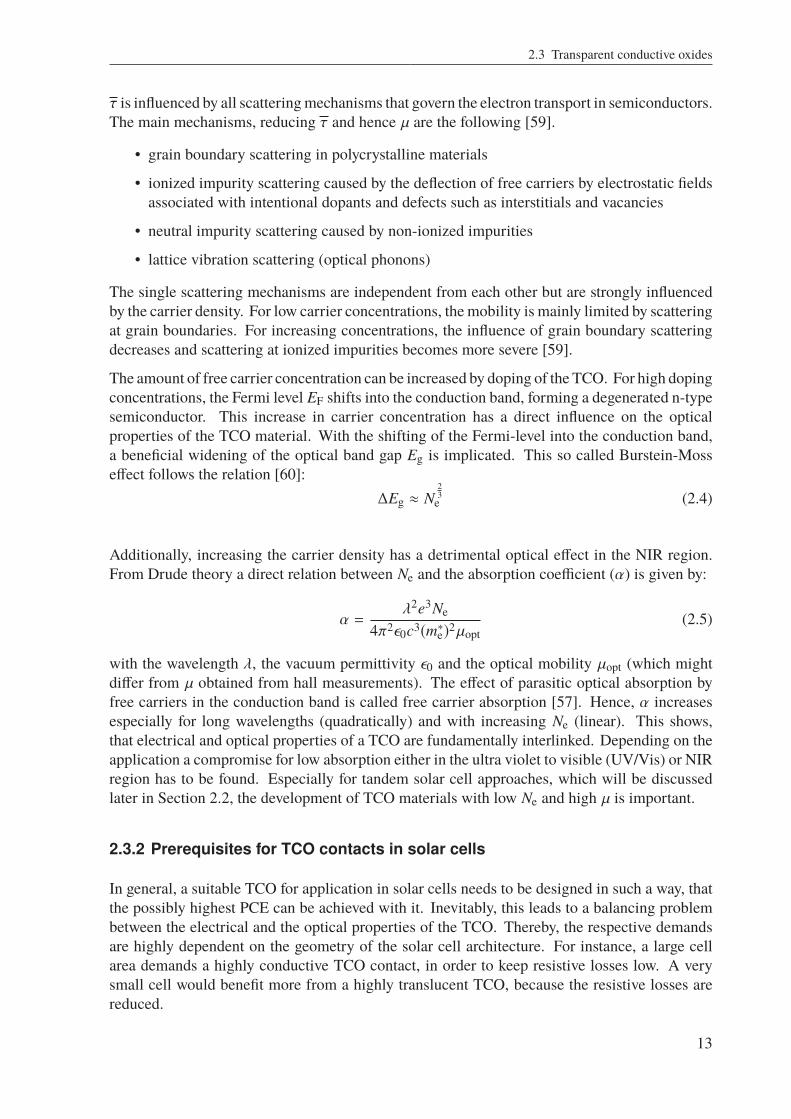
2.3.2 Prerequisites for TCO contacts in solar cells
In general, a suitable TCO for application in solar cells needs to be designed in such a way, thatthe possibly highest PCE can be achieved with it. Inevitably, this leads to a balancing problembetween the electrical and the optical properties of the TCO. Thereby, the respective demandsare highly dependent on the geometry of the solar cell architecture. For instance, a large cellarea demands a highly conductive TCO contact, in order to keep resistive losses low. A verysmall cell would benefit more from a highly translucent TCO, because the resistive losses arereduced.
13
2 Basics of perovskite- and tandem solar cells
For a given solar cell geometry, the optimization problem is reduced to finding the thicknessof the TCO layer that allows for an optimal balance between optical and electrical losses.Eventually, if good conductive properties are needed, a metal grid could be applied to increasethe conductivity. However, the implementation of a grid introduces additional shadowing lossesthat must be taken into account in the optimization process.
In tandem solar cells, the demands for the TCOs become more extended. The complete tandemcell needs a front TCO with high optical quality over a broader spectral range, because bothsubcells are more sensitive to losses in their share of the spectrum. TCOs that positioned inbetween both subcells need to be translucentmainly to lightwith longwavelengths. Furthermore,the thickness of all TCOs in tandem solar cells may be decreased, because the current densitiesproduced by the subcells are generally lower.
The following TCOs resemble materials, that are generally suitable for the high demands oftandem solar cells, because they offer good optical qualities over a broad spectrum with a decentconductivity. Next to the development of these TCOs, a major aspect of this thesis is theirimplementation into tandem cells. All optimization steps including thickness variations andgrid integration depend on the specific solar cell geometries that are used in this work.
2.3.3 Indium zinc oxide (IZO)
In contrast to traditional TCO materials, which are highly crystalline, IZO is an amorphousmaterial with good optoelectronic properties. It shows electron mobilities up to 60 cm2/V/sfor free densities between 1 × 1020 cm−3 to 3 × 1020 cm−3 and high optical transparency [61]and is therefore a suitable candidate for low NIR absorption transparent contact in solar celldevices. The doping of IZO is controlled by the amount of oxygen vacancies, as describedby Morales-Masis et al. [57]. Moreover it shows optical band gaps in the range of 3.44 eV to3.76 eV [62, 63] depending on the sputtering parameters. Since the deposition of amorphousIZO can be carried out by direct current (DC) or radio frequency (RF) magnetron sputteringat ambient temperatures and without any additional annealing steps, it is of great technologicalinterest for the application on temperature sensitive devices [64].
2.3.4 Hydrogen doped indium oxide (IO:H)
Recently, hydrogen-doped indium oxide (IO:H) has increasingly received considerable attentiondue to the high carrier mobilities reaching up to 130 cm2/Vs at moderate carrier concentrationsof below 2 × 1020 cm−3 [65]. Its optical transmittance is superior compared to commonlyused TCO materials like ITO or aluminium doped zinc oxide ZnxAl1– xO (ZAO) in both ultraviolet (UV) and NIR spectral ranges [66]. Koida et al. developed this material in 2007 by addingsmall amounts of water vapour during the sputter process of indium oxide (In2O3) [15,67]. In themeanwhile another approach was developed by introducing hydrogen gas instead of water duringthe process, because the introduction ofwater over a needle valve lacks in reproducibility [68,69].The presence of hydrogen is crucial for the growing of amorphous layers at room temperature andthementioned superior optical and electrical properties [69]. The bonding of hydroxide groups atindium atoms suppresses crystalline and favours amorphous growing. A subsequent annealing
14
2.4 Optics of single- and multi-junction solar cells
step at approximately 200 C induces solid-phase crystallization. The In(OH)3 transformsinto In2O3 due to water elimination. Additional hydrogen incorporation at grain boundariesis considered to passivate defects, hence reducing transport barriers and increasing carriermobility [66, 70].
2.3.5 Deposition of TCO thin films via magnetron sputtering
This section covers a basic introduction to important aspects of themagnetron sputtering process.Sputtering is a physical vapor deposition (PVD) method for thin film deposition. The basicprinciple is the removing of material from a target by accelerated ions from a glow discharge.The required plasma is generated by the application of electrical power to the target, technologicalrelevant are RF and DC power generators. The sputtering chamber with base pressures in theultra high vacuum (UHV) range, is filled with gas, typically with argon (Ar). The Ar+ ionsgenerated in the glow discharge are accelerated at the cathode fall (sheath) and sputter the targetresulting in the deposition of thin films on the substrate.
For magnetron sputtering, the electrical field is superposed with a magnetic field at the cathode,which forces the electrons in a cycloidalmotion and increases the collision rate between electrons.
If a reactive gas like oxygen (O2) is introduced into the chamber sputtering of thin films withdifferent compounds is possible. The reactive species not only adsorb on the substrate surface,but also lead to a compositional change of the surface target. Thus the partial pressure of reactivegas like oxygen in the chamber is a crucial parameter for the resulting thin film parameters. Inconclusion, the properties of deposited films is influenced by deposition parameters includingdeposition rate, substrate temperature, substrate material and deposition atmosphere [71, 72].
2.4 Optics of single- and multi-junction solar cells
For evaluation of the optical mechanisms that take place inside the multilayered structure ofa tandem solar cell, profound knowledge of the optical properties of the individual layers isnecessary. The following sections discuss the theoretical concepts that are used in this study toinvestigate these properties and how the knowledge is applied in the modelling and quantificationof spectral loss mechanisms.
2.4.1 Optical functions
The optical constants of a material are commonly described by the complex refractive indexN(λ) and the complex dielectric function ε(λ). They define the propagation of electromagneticwaves in media unambiguously and are related by:
ε(λ) = ε1(λ) − iε2(λ) = N(λ)2 = (n(λ) − ik(λ))2 (2.6)
where all quantities ε1(λ), ε2(λ) n(λ) and k(λ) are functions of the wavelength. The dielectricfunctions ε(λ) of dielectric materials can be described by the equations A.2 and A.3 in theappendix. The refractive index n represents the modification of the wavelength λ within amaterial, while the extinction coefficient k is representing the absorption of electromagnetic
15

2 Basics of perovskite- and tandem solar cells
waves. Real and imaginary part of both expressions are linked with each other by Kramers-Kronig relation. This means n and k are not independent, and can be calculated from each other.The Kramers-Kronig-consistency is one fundamental relation which has to be fulfilled for thedetermination of optical functions [73]. The imaginary part of the complex refractive index orextinction coefficient (k(λ)) may be also converted to the absorption coefficient (α) via equation2.7. More details are presented in the appendix A.1.
α =4πkλ
(2.7)
2.4.2 Reflection and transmission on multilayer structures
The optical properties of a (tandem) solar cell rely on real part of the complex refractive index orphase velocity (n(λ)) and k(λ) (or α) of each single layer and the individual film thickness (d).As a light beam travels through a layer, its initial intensity I = I0 gets attenuated following theLambert-Beer law
I = I0 · e−α(λ)d (2.8)
Because the attenuation scales with α and d, a high α is preferable for the absorbing layer, whilefor the other layers a low α is demanded in order to reduce parasitic absorption. This is usuallythe case for the semiconductor or dielectric materials, that are used in the solar cell. Of course,the prerequisite is a wide enough band gap of the material, because when interband transitionsare possible, fundamental absorption edges are observed with a drastic change of α. Also, therise of α due to free carrier absorption is critical in case of a high Ne, as it is observed in highlydoped layers such as in TCOs (compare Section 2.3.1).
At each interface between the layers, Fresnel reflection takes place. Usually during the measure-ments, the incident light is perpendicular to the solar cell surface. In that case, the reflectance (R)at the interface between the materials a and b is dependent on the respective na,b(λ):
R(λ) =(nb(λ) − na(λ)
nb(λ) + na(λ)
)2(2.9)
Fresnel reflection is of the most importance in the front- and rear interface of a semitransparentsolar cell, because of the great difference of the refractive indices between glass and air or TCOand air.
However, the solar cell consists of a multilayer stack with many interfaces and layer thicknessesin the range of visible light wavelengths. This causes a more complicated response of thetransmission or reflection of the device. When looking at a set of two interfaces and thesandwichedmaterial has a low α and the R values are high, multiple reflection is expected. Then,similar to a Fabry-Perot resonator, the distance between two plane parallel interfaces interfereswith coherent wavelengths of appropriate phases. There will be constructive interference, when
16

2.4 Optics of single- and multi-junction solar cells
an integer numberm of half waves fits into the resonator, and thus the transmission increases. Inthe opposite case, mainly destructive interference causes a rise in the reflection. The measuredtransmittance (T) and R responses of the devices will exhibit a series of interference minimaand maxima over the spectral range, originating from the internal multiple reflections.
The calculation of the internal reflection demands for a computational solution via transfermatrix method (TMM) [74] or other approaches using a direct extension of the Fabry-Perotresonator model [75]. All of the methods require a profound knowledge on the optical functionsof the layers and the respective thicknesses. A great uncertainty is introduced by the non ideallyflat interfaces (scattering) and partial intermixing of phases, e.g. the diffusion of material a intoa scaffold of material b (undefined n(λ) and k(λ)).
2.4.3 Measurement and simulation of optical losses in terms of current density
Experimentally, for a semitransparent sample such as a single TCO layer on glass or a completesemitransparent PSC, the R and T can be measured to calculate the absorptance (A) via
A = 1 − T − R. (2.10)
For opaque solar cells, T equals zero and the equation simplifies to
A = 1 − R. (2.11)
As discussed in the previous section, the R and T spectra of a thin layer or a set of thin layersexhibits interferences, which makes a comparison between samples of different thicknesses ormaterials quite difficult because of the shifting positions of the interference fringes.
In order to make the spectra comparable in a range between λ1 < λ2, an integration functionJ(λ1, λ2) is introduced, utilizing the current density equivalent of the photon flux (qNph) of theincident spectrum for weighting:
JTrn(λ1, λ2) =
∫ λ2
λ1
T · qNph dλ (2.12)
JAbs(λ1, λ2) =
∫ λ2
λ1
A · qNph dλ (2.13)
JRef(λ1, λ2) =
∫ λ2
λ1
R · qNph dλ (2.14)
The weighting by the photon flux, rather than the incident intensity is on purpose because theefficiency of a solar cell rather scales with the number of photons than with the energy thatthey carry. Especially in the long wavelength regime with less energetic photons, this makes asubstantial difference. By multiplication with the q, the unit conversion to a current density withthe units mA cm−2 is achieved. This is not only more practical than comparing large particleflux numbers, but it has a direct relation to the photovoltaic application, since the photo currentdensity obtained by EQE measurement (JEQE) is calculated in the same manner:
17

2 Basics of perovskite- and tandem solar cells
JEQE =∫
EQE · qNph dλ (2.15)
By creating the ratio of current density equivalent of the transmission (JTrn) and the integralof qNph, a single weighted average transmittance (Twt) value for the chosen spectral range ispresented:
Twt(λ1, λ2) =JTrn(λ1, λ2)∫ λ2λ1
qNph dλ. (2.16)
In analogy the same may be performed for the current density equivalent of the parasiticabsorption loss (JAbs) with a weighted average absorptance (Awt):
Awt(λ1, λ2) =JAbs(λ1, λ2)∫ λ2λ1
qNph dλ. (2.17)
The measured values of the T and R only allow an outside view on the mechanisms inside thePSC, indicating the sum of the manifold internal reflections. Measuring the external quantumefficiency (EQE) of a solar cell, allows for further assessment of the parasitic losses that areintroduced by the single layers. A principle EQE investigation is shown in Figure 2.9 for anopaque solar cell. It demonstrates how the EQE of a solar cell is qualitatively affected, whenadditional layers are implemented in the architecture.
18

2.4 Optics of single- and multi-junction solar cells
Insufficient absorption
Recombination
Free carrier absorptionInterband transition
Figure 2.9: Schematic illustration of the EQE spectrum under variation of the solar cell architecture. Originalgraphic from Fujiwara et al. [76]. a) Hypothetical perfect absorber without R, b) Absorber/metalinterface with losses due to reflection and insufficient absorption of photons with long wavelengths thatare lost to the metal rear interface, c) TCO/absorber/metal with additional parasitic absorption in theTCO, d) TCO/doped layer/absorber/metal with losses due to the narrow absorption edge of the dopedlayer, e) the similar architecture with a recombination layer at the rear interface with the metal.
19
2 Basics of perovskite- and tandem solar cells
It shows that the EQE is affected by optical effects, such as reflection (b) and parasitic absorptionin TCOs (c) and doped interlayers (d). Additionally, it demonstrates, how insufficient absorptionin the absorber (b) and increased recombination at the rear interface (e) reduce the EQE response.These effects are difficult to distinguish without the knowledge of the absorption in each singlelayer.
However, a quantitative statement about the individual contribution of each sublayer to the totalJAbs is only possible with aforementioned computational methods. Here, the program e-ARC isused to carry out a TMM based simulation of the tandem architecture. A comprehensive studyon the methods and functionalities provided in e-ARC is presented by Fujiwara et al. [76].
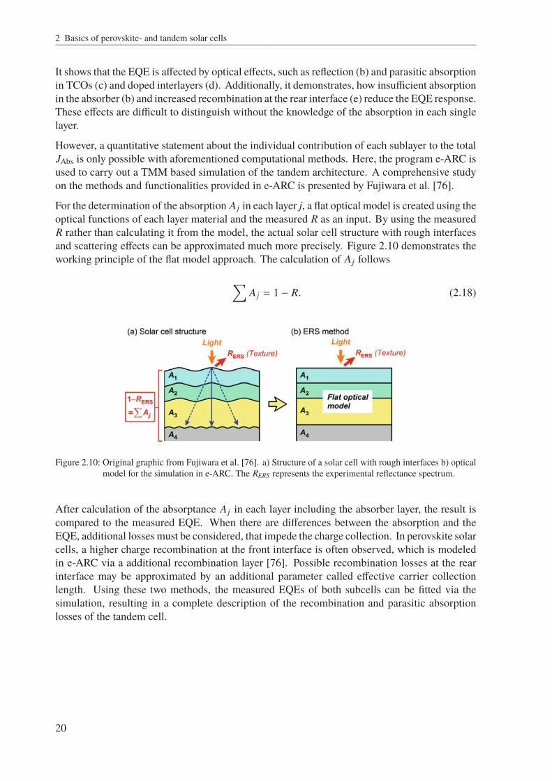
For the determination of the absorption A j in each layer j, a flat optical model is created using theoptical functions of each layer material and the measured R as an input. By using the measuredR rather than calculating it from the model, the actual solar cell structure with rough interfacesand scattering effects can be approximated much more precisely. Figure 2.10 demonstrates theworking principle of the flat model approach. The calculation of A j follows∑
A j = 1 − R. (2.18)
Figure 2.10: Original graphic from Fujiwara et al. [76]. a) Structure of a solar cell with rough interfaces b) opticalmodel for the simulation in e-ARC. The RERS represents the experimental reflectance spectrum.
After calculation of the absorptance A j in each layer including the absorber layer, the result iscompared to the measured EQE. When there are differences between the absorption and theEQE, additional losses must be considered, that impede the charge collection. In perovskite solarcells, a higher charge recombination at the front interface is often observed, which is modeledin e-ARC via a additional recombination layer [76]. Possible recombination losses at the rearinterface may be approximated by an additional parameter called effective carrier collectionlength. Using these two methods, the measured EQEs of both subcells can be fitted via thesimulation, resulting in a complete description of the recombination and parasitic absorptionlosses of the tandem cell.
20

2.5 Structural analysis of thin films with XRD
2.5 Structural analysis of thin films with XRD
Being a powerful tool for thin film analysis, a typical x-ray diffraction (XRD) pattern contains avariety of information:
• Peak position: Identification of phases, structures and lattice parameters
• Peak width: Information about the crystallite size, microstrain and defects
• Peak area or intensity ratio: Determination of a preferential crystal orientation
• Peak tails: Diffuse scattering and point defects
• Background: Amorphous contents
In its basic application, XRD is used for detection of the characteristic diffraction pattern of aphase and determination of the corresponding crystal structure from the peak positions. Thetechnique is well-known and will not be explained in more detail at this point.
However, the evaluation of the crystallite size or strain from the width and shape of the diffractedpeaks requires further calculation steps, which will be briefly discussed here.
Also, special considerations for XRD measurements under grazing incidence angles will behighlighted.
2.5.1 Williamson-Hall analysis
The observed breadth of a diffracted peak may be described by its full width at half maximum(FWHM), which is a convolution of the structural diffraction peak broadening (FWHMstruct)of the specimen and instrumental diffraction peak broadening (FWHMinst) due to the opticalsetup [77]:
FWHM = FWHMstruct + FWHMinst (2.19)
The FWHMstruct of a specimen is obtained by correction of the measured FWHM with theFWHMinst. The latter is usually determined by measuring a reference standard material thatshows no structural broadening with the same optical parameters.
Following Scherrer’s equation [78] for crystallite size related broadening, including the peakbroadening due to microstrains, the FWHMstruct calculates to
FWHMstruct =Kλ
Lcosθ+ 4ε
sinθcosθ
(2.20)
with the Scherrer constant (K), the crystallite size (L), the wavelength (λ), the diffracted angle(θ), and the microstrain (ε).
21

2 Basics of perovskite- and tandem solar cells
From this relation, the Williamson-Hall equation is obtained in the form y = a + bx, which canbe used to determine the amount of crystallite size broadening (a) and microstrain broadening(b), when fitting a linear regression to the observed FWHMstruct:
FWHMstruct · cosθ =KλL︸︷︷︸
crystallite size
+ 4ε︸︷︷︸microstrain
·sinθ (2.21)
2.5.2 Grazing incidence XRD
In grazing incidence x-ray diffraction (GIXRD), a highly asymmetric Bragg measurementgeometry is used with an incident angle (ω) below or close to the critical angle (ωc), typicallyin the range of 0.1° to 3°. Under the conditions of total reflection, Bragg diffraction takes placeonly at the very surface of the sample. With increasing ω, the beam penetrates deeper into thelayer, enabling a depth scan of the film thickness. The penetration depth (τ) depends on themeasurement geometry and the material properties. ω defines the travel path length of the beamthrough the layer and the linear attenuation coefficient (µatt) of the material is used to calculatethe amount of attenuation regarding the Lambert-Beer law. The calculation of τ follows [79]
τ =
√2λ
4π
(((ω2 − ω2
c)2 + β
)− 12− (ω2 − ω2
c)
) 12
(2.22)
with β = λµatt/4π being the imaginary part of the refractive index (N = 1 − δ − iβ). Thepenetration depth into a In2O3 layer is shown in Figure 4.19 and is e.g. ≈2 nm at an angle of0.3° and ≈100 nm at 0.9°.
At low angles around ωc, the incident x-ray beam gets refracted at the sample surface by asignificant amount, resulting in a angular change of the beam direction in the material. Inconsequence the observed diffracted peaks are shifted from the expected Bragg positions by anangle of 2∆θ. The shift may be as high as several tenths of degrees at its maximum at ωc, so inorder to prevent misinterpretation, the observed peak positions must be corrected by 2∆θ [80]
2∆θ = ω −1√
2
(((ω2 − ω2
c)2 + 4β2
) 12− (ω2 − ω2)
) 12
. (2.23)
22
3 Experimental methods for preparation andcharacterization of perovskite-CIGS tandem cells
The first part of this chapter describes the preparation techniques that are used for PSCs and thecorresponding layers. It is divided into three sections, that cover the solution based methods(Section 3.1.1), the PVD by thermal evaporation (Section 3.1.2) and by sputtering (Section3.1.3).
The second part introduces the analyticalmethods that are utilized for the general characterizationof thin films (Section 3.2.1) and for evaluation of the optical and electrical performance of solarcells (Section 3.2.2).
3.1 Preparation of perovskite solar cells
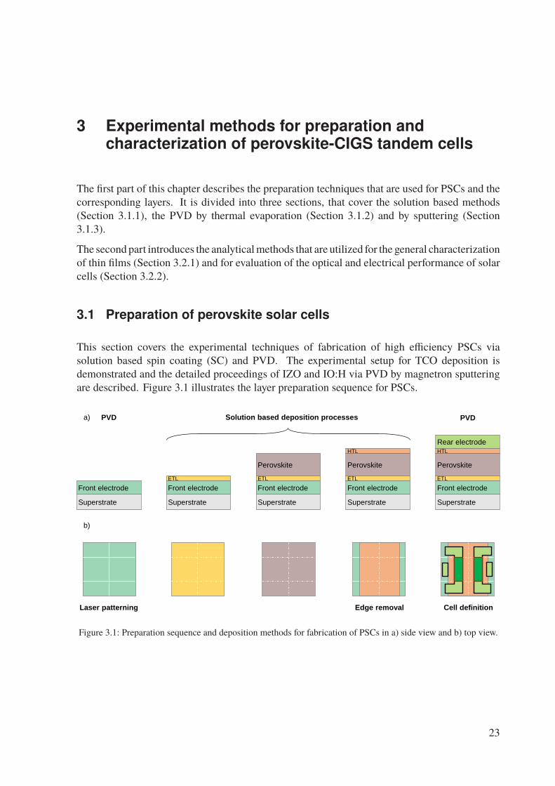
This section covers the experimental techniques of fabrication of high efficiency PSCs viasolution based spin coating (SC) and PVD. The experimental setup for TCO deposition isdemonstrated and the detailed proceedings of IZO and IO:H via PVD by magnetron sputteringare described. Figure 3.1 illustrates the layer preparation sequence for PSCs.
Superstrate
Front electrode
Superstrate
ETL
Front electrode
Superstrate
Perovskite
ETL
Front electrode
Superstrate
HTL
Perovskite
ETL
Front electrode
Superstrate
HTL
Perovskite
ETL
Rear electrode
Front electrode
PVD Solution based deposition processes PVDa)
b)
Laser patterning Edge removal Cell definition
Figure 3.1: Preparation sequence and deposition methods for fabrication of PSCs in a) side view and b) top view.
23
3 Experimental methods for preparation and characterization of perovskite-CIGS tandem cells
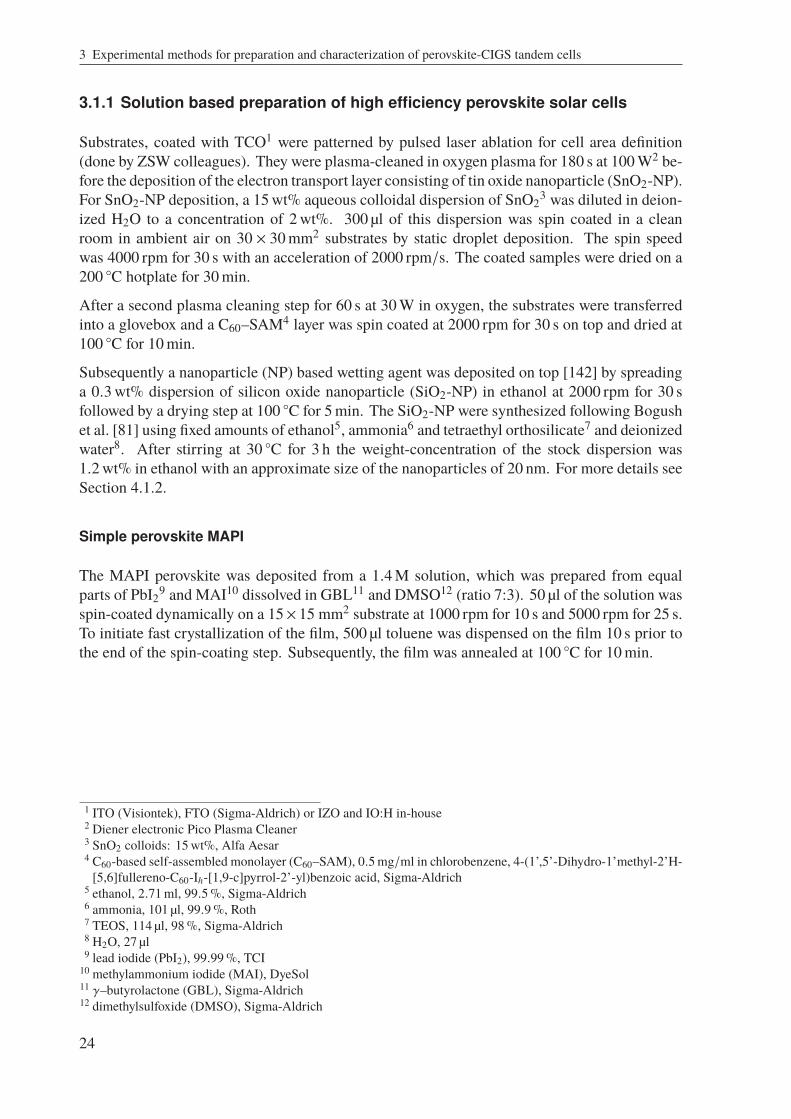
3.1.1 Solution based preparation of high efficiency perovskite solar cells
Substrates, coated with TCO1 were patterned by pulsed laser ablation for cell area definition(done by ZSW colleagues). They were plasma-cleaned in oxygen plasma for 180 s at 100 W2 be-fore the deposition of the electron transport layer consisting of tin oxide nanoparticle (SnO2-NP).For SnO2-NP deposition, a 15 wt% aqueous colloidal dispersion of SnO2
3 was diluted in deion-ized H2O to a concentration of 2 wt%. 300 µl of this dispersion was spin coated in a cleanroom in ambient air on 30 × 30 mm2 substrates by static droplet deposition. The spin speedwas 4000 rpm for 30 s with an acceleration of 2000 rpm/s. The coated samples were dried on a200 C hotplate for 30 min.
After a second plasma cleaning step for 60 s at 30 W in oxygen, the substrates were transferredinto a glovebox and a C60–SAM4 layer was spin coated at 2000 rpm for 30 s on top and dried at100 C for 10 min.
Subsequently a nanoparticle (NP) based wetting agent was deposited on top [142] by spreadinga 0.3 wt% dispersion of silicon oxide nanoparticle (SiO2-NP) in ethanol at 2000 rpm for 30 sfollowed by a drying step at 100 C for 5 min. The SiO2-NP were synthesized following Bogushet al. [81] using fixed amounts of ethanol5, ammonia6 and tetraethyl orthosilicate7 and deionizedwater8. After stirring at 30 C for 3 h the weight-concentration of the stock dispersion was1.2 wt% in ethanol with an approximate size of the nanoparticles of 20 nm. For more details seeSection 4.1.2.
Simple perovskite MAPI
The MAPI perovskite was deposited from a 1.4 M solution, which was prepared from equalparts of PbI29 and MAI10 dissolved in GBL11 and DMSO12 (ratio 7:3). 50 µl of the solution wasspin-coated dynamically on a 15× 15 mm2 substrate at 1000 rpm for 10 s and 5000 rpm for 25 s.To initiate fast crystallization of the film, 500 µl toluene was dispensed on the film 10 s prior tothe end of the spin-coating step. Subsequently, the film was annealed at 100 C for 10 min.
1 ITO (Visiontek), FTO (Sigma-Aldrich) or IZO and IO:H in-house2 Diener electronic Pico Plasma Cleaner3 SnO2 colloids: 15 wt%, Alfa Aesar4 C60-based self-assembled monolayer (C60–SAM), 0.5 mg/ml in chlorobenzene, 4-(1’,5’-Dihydro-1’methyl-2’H-[5,6]fullereno-C60-Ih-[1,9-c]pyrrol-2’-yl)benzoic acid, Sigma-Aldrich
5 ethanol, 2.71 ml, 99.5 %, Sigma-Aldrich6 ammonia, 101 µl, 99.9 %, Roth7 TEOS, 114 µl, 98 %, Sigma-Aldrich8 H2O, 27 µl9 lead iodide (PbI2), 99.99 %, TCI10 methylammonium iodide (MAI), DyeSol11 γ–butyrolactone (GBL), Sigma-Aldrich12 dimethylsulfoxide (DMSO), Sigma-Aldrich
24
3.1 Preparation of perovskite solar cells
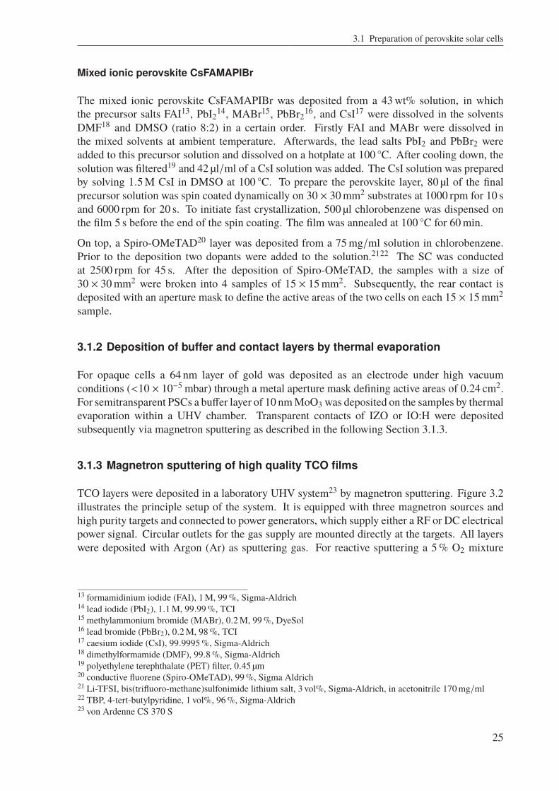
Mixed ionic perovskite CsFAMAPIBr
The mixed ionic perovskite CsFAMAPIBr was deposited from a 43 wt% solution, in whichthe precursor salts FAI13, PbI214, MABr15, PbBr216, and CsI17 were dissolved in the solventsDMF18 and DMSO (ratio 8:2) in a certain order. Firstly FAI and MABr were dissolved inthe mixed solvents at ambient temperature. Afterwards, the lead salts PbI2 and PbBr2 wereadded to this precursor solution and dissolved on a hotplate at 100 C. After cooling down, thesolution was filtered19 and 42 µl/ml of a CsI solution was added. The CsI solution was preparedby solving 1.5 M CsI in DMSO at 100 C. To prepare the perovskite layer, 80 µl of the finalprecursor solution was spin coated dynamically on 30 × 30 mm2 substrates at 1000 rpm for 10 sand 6000 rpm for 20 s. To initiate fast crystallization, 500 µl chlorobenzene was dispensed onthe film 5 s before the end of the spin coating. The film was annealed at 100 C for 60 min.
On top, a Spiro-OMeTAD20 layer was deposited from a 75 mg/ml solution in chlorobenzene.Prior to the deposition two dopants were added to the solution.2122 The SC was conductedat 2500 rpm for 45 s. After the deposition of Spiro-OMeTAD, the samples with a size of30 × 30 mm2 were broken into 4 samples of 15 × 15 mm2. Subsequently, the rear contact isdeposited with an aperture mask to define the active areas of the two cells on each 15 × 15 mm2
sample.
3.1.2 Deposition of buffer and contact layers by thermal evaporation
For opaque cells a 64 nm layer of gold was deposited as an electrode under high vacuumconditions (<10 × 10−5 mbar) through a metal aperture mask defining active areas of 0.24 cm2.For semitransparent PSCs a buffer layer of 10 nmMoO3 was deposited on the samples by thermalevaporation within a UHV chamber. Transparent contacts of IZO or IO:H were depositedsubsequently via magnetron sputtering as described in the following Section 3.1.3.
3.1.3 Magnetron sputtering of high quality TCO films
TCO layers were deposited in a laboratory UHV system23 by magnetron sputtering. Figure 3.2illustrates the principle setup of the system. It is equipped with three magnetron sources andhigh purity targets and connected to power generators, which supply either a RF or DC electricalpower signal. Circular outlets for the gas supply are mounted directly at the targets. All layerswere deposited with Argon (Ar) as sputtering gas. For reactive sputtering a 5 % O2 mixture
13 formamidinium iodide (FAI), 1 M, 99 %, Sigma-Aldrich14 lead iodide (PbI2), 1.1 M, 99.99 %, TCI15 methylammonium bromide (MABr), 0.2 M, 99 %, DyeSol16 lead bromide (PbBr2), 0.2 M, 98 %, TCI17 caesium iodide (CsI), 99.9995 %, Sigma-Aldrich18 dimethylformamide (DMF), 99.8 %, Sigma-Aldrich19 polyethylene terephthalate (PET) filter, 0.45 µm20 conductive fluorene (Spiro-OMeTAD), 99 %, Sigma Aldrich21 Li-TFSI, bis(trifluoro-methane)sulfonimide lithium salt, 3 vol%, Sigma-Aldrich, in acetonitrile 170 mg/ml22 TBP, 4-tert-butylpyridine, 1 vol%, 96 %, Sigma-Aldrich23 von Ardenne CS 370 S
25
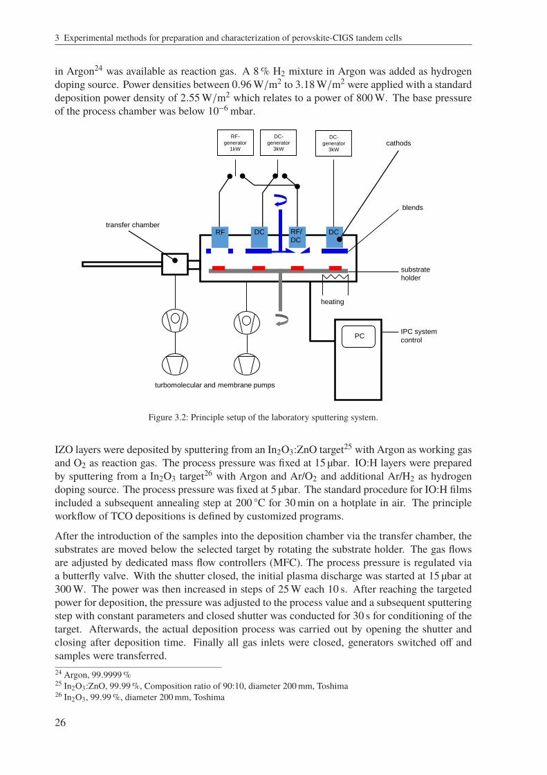
3 Experimental methods for preparation and characterization of perovskite-CIGS tandem cells
in Argon24 was available as reaction gas. A 8 % H2 mixture in Argon was added as hydrogendoping source. Power densities between 0.96 W/m2 to 3.18 W/m2 were applied with a standarddeposition power density of 2.55 W/m2 which relates to a power of 800 W. The base pressureof the process chamber was below 10−6 mbar.
blends
substrateholder
cathods
IPC system
control
transfer chamberRF DC RF/
DCDC
RF-
generator1kW
DC-
generator3kW
DC-
generator3kW
turbomolecular and membrane pumps
PC
heating
Figure 3.2: Principle setup of the laboratory sputtering system.
IZO layers were deposited by sputtering from an In2O3:ZnO target25 with Argon as working gasand O2 as reaction gas. The process pressure was fixed at 15 µbar. IO:H layers were preparedby sputtering from a In2O3 target26 with Argon and Ar/O2 and additional Ar/H2 as hydrogendoping source. The process pressure was fixed at 5 µbar. The standard procedure for IO:H filmsincluded a subsequent annealing step at 200 C for 30 min on a hotplate in air. The principleworkflow of TCO depositions is defined by customized programs.
After the introduction of the samples into the deposition chamber via the transfer chamber, thesubstrates are moved below the selected target by rotating the substrate holder. The gas flowsare adjusted by dedicated mass flow controllers (MFC). The process pressure is regulated viaa butterfly valve. With the shutter closed, the initial plasma discharge was started at 15 µbar at300 W. The power was then increased in steps of 25 W each 10 s. After reaching the targetedpower for deposition, the pressure was adjusted to the process value and a subsequent sputteringstep with constant parameters and closed shutter was conducted for 30 s for conditioning of thetarget. Afterwards, the actual deposition process was carried out by opening the shutter andclosing after deposition time. Finally all gas inlets were closed, generators switched off andsamples were transferred.24 Argon, 99.9999 %25 In2O3:ZnO, 99.99 %, Composition ratio of 90:10, diameter 200 mm, Toshima26 In2O3, 99.99 %, diameter 200 mm, Toshima
26

3.2 Characterization methods for solar cells
All films for characterizationwere deposited on cleaned borosilicate glass27 as substratematerial.TCO layers for the application in PSC as superstrates or substrates were grown on 1.1 mmborosilicate glass. The transparent back contacts of PSCs were deposited through a metalaperture mask with the same layout as used for the gold references.
3.2 Characterization methods for solar cells
This study comprises a variety of analytical methods for characterization of the optical, electricaland structural properties of thin films and complete solar cells. The corresponding experimentalsetups and measurement parameters are described in the following sections.
3.2.1 Thin film characterization
This section covers the experimental techniques for the characterization of thin films. Hereinthe most important analysis techniques are UV/Vis to determine transmittance and reflectanceand four-point-probe (4P) measurements to determine the sheet resistance of conductive filmssuch as TCOs. For detailed analysis of specific optical, electrical or structural proberties, Hallmeasurements, XRD, spectroscopic ellipsometry (SE), scanning electron microscopy (SEM)and confocal laser scanning microscopy (CLSM) were carried out.
UV/Vis for the determination of optical properties and film thickness
In order to analyze the optical properties of the films their transmittance T and reflectance Rspectra were measured with an Ulbricht-sphere setup in a Perkin Elmer Lambda 900 Spectrom-eter. From this the absorptance A was calculated via A = 100 − R − T . The weighted averagetransmittance (Twt) and weighted average absorptance (Awt) are then calculated via equations2.16 and 2.17.
For the absorption edge calculation of TCOmaterials, the absorption coefficient αwas calculatedby following equation:
α =1d· ln
1 − R2
T(3.1)
with the layer thickness d [82, 83]. The direct optical band gap Eg is extracted from a Tauc-plot where (αhν)2 is plotted over hν and h is the Planck constant and ν the frequency of theelectromagnetic field. Eg can be estimated by the intercept of (αhν)2 = 0 of a linear regressionfollowing the equation
(αhν)2 = A(hν − Eg) (3.2)
where A is a constant [83, 84].
From transmittance spectra thicknesses of the thin filmswere determined by an optical simulationwith a computational software for data processing and visualization (Diplot), based on the patternof interference [85].
27 borosilicate, D263 T, 0.55 mm, Schott
27
3 Experimental methods for preparation and characterization of perovskite-CIGS tandem cells
4-point probe to determine sheet resistances
The sheet resistance was measured with a Jandel four-point-probe, in the in-line 4P geometrywith the distance s between the contacts. The voltage V between the two inner contacts ismeasured while a current I is injected through the outer contacts. The measured resistanceR = V
I corresponds only to the sample resistance and is independent of any contact and wiringresistances. For the ideal case with d << s and infinitely large thin film surface, where d is thefilm thickness, the sheet resistance Rsheet is defined by
Rsq =ρ
d=
π
ln2·
VI
(3.3)
with the resistivity ρ. [86]. In order to indicate a sheet resistance value, the unit is given as[Rsq] = Ω.
Hall measurements for investigating the charge transport
For a detailed electrical characterization Hall measurements were carried out. The measurementis based on the deflection of charge carriers with a velocity perpendicular to a magnetic fieldB which generates a measurable voltage. From this voltage resistivity ρ, carrier concentrationNe and carrier mobility µ are obtained [87]. Therefore TCO samples were cutted into a size of1 × 1 cm2 and contacted in the corners. The measurements were performed with a PhysTechRH2010 system in van der Pauw configuration at a magnet field of B = 0.5 T and differentcurrents of 0.1 mA, 1 mA and 10 mA.
X-ray diffraction for structural analysis
For crystallographical analysis XRD measurements (2θ-scans, 10° to 70°) were performed witha Panalytical Empyrean system in Bragg-Brentano geometry with a CuKα line as radiationsource. Acceleration voltage and current were set to 40 V and 40 µA, respectively. The GIXRDmeasurements were performed at different ω ranging from 0.1° to 3° with the same current andvoltage parameters. The used software was Highscore version 3.
Spectroscopic ellipsometry to determine optical functions
Spectroscopic ellipsometry (SE) measurements were performed with a Sentech SE800 PVsystem in order to determine the optical functions n(λ) and k(λ) of the PSC layers. Allinvestigated layers were deposited on quartz glass. The SE spectra of the polarization angles Ψand ∆ were measured in a range from 280 nm to 1630 nm for six different incidence angles Φbetween 50° to 75° in steps of 5°. The measurements and the subsequent simulation of n(λ) andk(λ) were carried out by Tim Helder with the software SpectraRay 4 from Sentech. Detailedinformation of the ellipsometry models and the model parameters are given in the appendix A.1.
28

3.2 Characterization methods for solar cells
Scanning electron microscopy
SEM images of surfaces and cross sections were taken with a FEI Sirion XL30S FEG at a voltageof 5 kV. Measurements were carried out by Tina Wahl and Daniela Müller.
Confocal laser scanning microscopy
Confocal laser scanning microscopy images were taken with a Keyence VK-9700K Color 3DLaser Microscope. The software for image processing was VK Analyzer from Keyence.
Contact angle measurements
Droplets of the perovskite precursor solution (3 µl) were applied on top of the sample surface.A customized setup was used to take photographs of contact angles inside a nitrogen-filledglovebox. The program ImageJ [88]with the contact anglemeasurement tool byMarcoBrugnara[89] was used for evaluation of the data and contact angle fitting.
3.2.2 Solar cell analysis
For the characterization of the photovoltaic performance and the spectral response of the solarcells, JV measurements, EQE spectroscopy and current loss analyses were conducted.
Current-voltage characterization
The photovoltaic device performance was measured with a Keithley 2400 source meter at a scanspeed of 0.2 V/s under ambient conditions and illumination of standard test conditions by aWacom WXS-90S-L2 Super Solar Simulator (class AAA, AM 1.5G, 1000 W/m2). All deviceswere prebiased at 1.5 V for 5 s and measured from 1.5 V to −0.2 V (rvs) and from −0.2 V to1.5 V (fwd).
The JV response is used to obtain the characteristic solar cell parameters short circuit currentdensity (JSC), VOC, FF, MPP and consequently the PCE.
Generally, the PCE is defined as the ratio of the incident radiative power of the AM1.5G solarspectrum (AM1.5) Pin at standard test conditions (25 C, normal incidence) and the maximumgenerated electrical power output Pmax and it is connected to the other parameters via
PCE =PmaxPin=
FF · VOC · ISCPin
(3.4)
.
Due to the hysteresis in the PSCs, the PCE obtained from the fwd and from the rvs scan is namedPCE f wd and PCErvs, respectively. The same holds for steady state efficiencies obtained fromMPP tracking which are labelled PCEMPP. Compare also Section 2.1.3.
When a CIGS cell is not illuminated by AM1.5 but by the transmission spectrum of a PSC topcell (’filtered’) the notation follows PCEf.
29
3 Experimental methods for preparation and characterization of perovskite-CIGS tandem cells
Quantum efficiency
The external quantum efficiency (EQE) was determined with a Bentham PVE 300. The spectralrange of measurement for the tandem cells was from 300 nm to 1300 nm. The setup wascalibrated with standardized silicon (300 nm to 1100 nm) and germanium (800 nm to 1600 nm)photodiodes prior to the measurements. A measurement spot size of 0.05 cm2 was chosen inorder to fit between the grid bars of the solar cells. Additional details of the measurements aregiven in the appendix A.2.
Current loss analysis with e-ARC
The current loss analysis and EQE simulation was performed with the program e-ARC v2.0 byAIST [90]. The layer stack model of the tandem solar cell was created using the optical functions(n(λ), k(λ)) obtained from SE measurements in Section 5.4.1, as well as from literature data forITO (N = 1.2 × 1021 cm−3) [91], spiro-OMeTAD [92], air [93], CIGS [94], MoSe [95], andmolybdenum, MgF2, CdS, and i-ZnO [96].
30

4 Development of perovskite solar cells for tandemapplication
The first central part of this study is the development of the perovskite top cell for applicationin tandem cells. Figure 4.1 depicts the branch of the strategy chart from Chapter 1, thatis schematically explaining the development of the top cell in standard n-type–intrinsic–p-type (n-i-p) configuration. The chapter is divided into three main sections, that guide throughthe principle development process from comparably simple and low performing, opaque solarcells to more complex and highly efficient, semitransparent solar cells.
4.1 Opaque
4. Perovskite Top Cell
4.3 Semitransparent
Top Cell
Opaque Electrode
Transparent Electrode
ETL
FTO
4.2 Transparent electrode
SnO2
IO:H
Perovskite
IZOGold
other
ITO
FullerenesABX3 Perovskite
Substrate/Superstrate IO:H
MoO3Amide
Multi Cation
IZOTiO2
HTLTandemintegration
Wetting Agent
Buffer Layer Wide Band Gap
Spiro
Figure 4.1: Strategy for developing the n-i-p–perovskite top cell.
The first section 4.1 focuses on the most important steps in the optimization of the electrical per-formance of single perovskite cells. Most of this work is related to the materials and interfaces atthe electron selective layer and has been predominantly but not exclusively conducted on opaquecells with a metal back contact. Highlights are the evaluation of different TCO-ETL-absorbercombinations, the introduction of fullerenes for hysteresis suppression and the development ofa nanoparticle based interlayer for enhanced wetting on hydrophobic interfaces.
Secondly in Section 4.2, for the transition to semitransparent solar cells, the sputter depositionof suitable transparent and conductive layers of IO:H and IZO is discussed. For the designatedapplication as front and rear electrodes in the top cell, the demanded material properties are ahigh conductivity and a low absorption. Special focus lies on post deposition crystallization ofthe promising IO:H, which allows for a superiorly low NIR absorption.
31

4 Development of perovskite solar cells for tandem application
The subsequent Section 4.3 evaluates the implementation of the TCOs into the PSC architecture.An important step is the damage-free sputter deposition of a TCO layer as rear electrode ontothe perovskite cell, replacing the opaque metal electrode. Major optical advantages are expectedfrom the replacement of the traditional front electrodes ITO or FTO. With the adjustment ofthe TCO layer thicknesses, the semitransparent PSC are finally prepared for the implementationinto tandem devices.
4.1 Opaque perovskite solar cells
This section is devoted to the implementation, optimization and evaluation of different materialsin the development of opaque perovskite solar cells towards a high efficiency. The aim of thesection is a successive advancement of the opaque solar cells in order to prepare them for thetransition to semitransparent architectures.
In the n-type–intrinsic–p-type (n-i-p) perovskite solar cell, the n-type layer is on the lightincident side as seen in Figure 4.2. Due to the superstrate setup of PSCs the n-layer is aboutto be deposited at first in the production process of the solar cell stack. Since the subsequentlayers have to be deposited on top of the n-layer, it is influencing the following film qualityand morphology. It is reasonable to begin with optimizing the n-interface and to proceed withthe absorber material, then the p-type and finally the electrode materials, because any changein the very first layers may require a re-optimization of all the layers that follow on top of it.For this reason, this section begins with a brief evaluation of a simple glass/TCO/ETL/absorbercombination in Section 4.1.1.
Section 4.1.2 introduces a new approach based on nanoparticles to enhance the wettability ofhydrophobic interfaces. This is needed for the subsequent implementation of desirable fullereneinterlayers, which are often of a hydrophobic nature. Their repellent behaviour causes severe de-wetting issues in the attempt to deposit a perovskite layer by sin coating on top of it. The workingprinciple of the wetting agent is mainly investigated by means of contact angle measurements.
Section 4.1.3 discusses the beneficial effects of fullerene interlayers for the perovskite solarcell performance. Furthermore, a mixed cation perovskite is introduced, that shall increase theefficiency of the opaque solar cells.
32
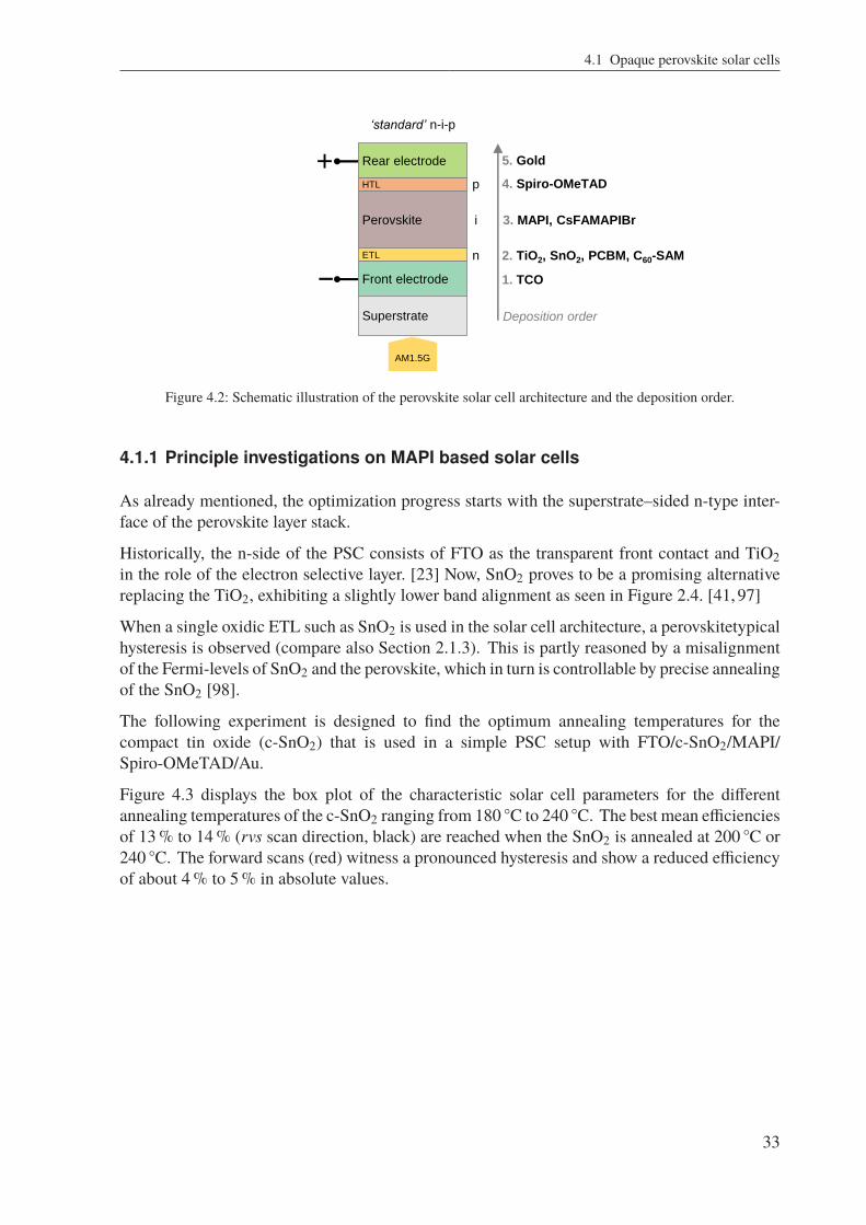
4.1 Opaque perovskite solar cells
‘standard’ n-i-p
Superstrate
HTL
Perovskite
ETL
Rear electrode
Front electrode
+
−
p
n
5. Gold
4. Spiro-OMeTAD
2. TiO2, SnO2, PCBM, C60-SAM
1. TCO
i
AM1.5G
3. MAPI, CsFAMAPIBr
Deposition order
Figure 4.2: Schematic illustration of the perovskite solar cell architecture and the deposition order.
4.1.1 Principle investigations on MAPI based solar cells
As already mentioned, the optimization progress starts with the superstrate–sided n-type inter-face of the perovskite layer stack.
Historically, the n-side of the PSC consists of FTO as the transparent front contact and TiO2in the role of the electron selective layer. [23] Now, SnO2 proves to be a promising alternativereplacing the TiO2, exhibiting a slightly lower band alignment as seen in Figure 2.4. [41, 97]
When a single oxidic ETL such as SnO2 is used in the solar cell architecture, a perovskitetypicalhysteresis is observed (compare also Section 2.1.3). This is partly reasoned by a misalignmentof the Fermi-levels of SnO2 and the perovskite, which in turn is controllable by precise annealingof the SnO2 [98].
The following experiment is designed to find the optimum annealing temperatures for thecompact tin oxide (c-SnO2) that is used in a simple PSC setup with FTO/c-SnO2/MAPI/Spiro-OMeTAD/Au.
Figure 4.3 displays the box plot of the characteristic solar cell parameters for the differentannealing temperatures of the c-SnO2 ranging from 180 C to 240 C. The best mean efficienciesof 13 % to 14 % (rvs scan direction, black) are reached when the SnO2 is annealed at 200 C or240 C. The forward scans (red) witness a pronounced hysteresis and show a reduced efficiencyof about 4 % to 5 % in absolute values.
33
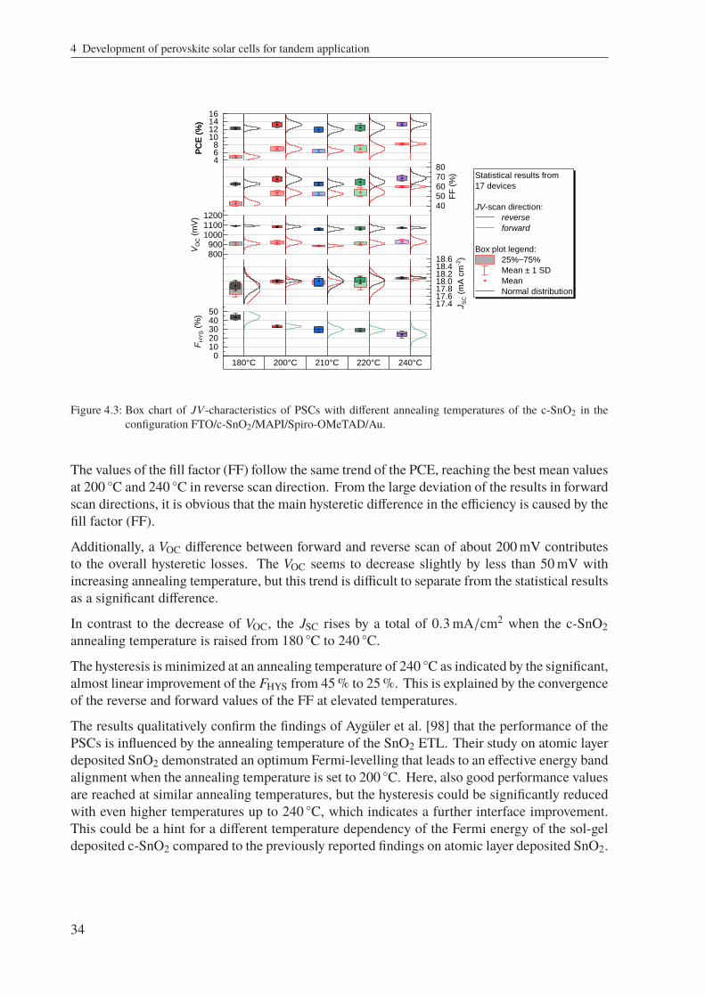
4 Development of perovskite solar cells for tandem application
PC
E (
%)
Statistical results from
17 devices
JV-scan direction:
reverse
forward
Box plot legend:
25%~75%
Mean ± 1 SD
Mean
Normal distribution
468
10121416
PC
E (
%)
4050607080
FF
(%
)
800900
100011001200
VO
C (
mV
)
17.417.617.818.018.218.418.6
JS
C (
mA
cm
-2)
180°C 200°C 210°C 220°C 240°C0
1020304050
FH
YS (
%)
Figure 4.3: Box chart of JV-characteristics of PSCs with different annealing temperatures of the c-SnO2 in theconfiguration FTO/c-SnO2/MAPI/Spiro-OMeTAD/Au.
The values of the fill factor (FF) follow the same trend of the PCE, reaching the best mean valuesat 200 C and 240 C in reverse scan direction. From the large deviation of the results in forwardscan directions, it is obvious that the main hysteretic difference in the efficiency is caused by thefill factor (FF).
Additionally, a VOC difference between forward and reverse scan of about 200 mV contributesto the overall hysteretic losses. The VOC seems to decrease slightly by less than 50 mV withincreasing annealing temperature, but this trend is difficult to separate from the statistical resultsas a significant difference.
In contrast to the decrease of VOC, the JSC rises by a total of 0.3 mA/cm2 when the c-SnO2annealing temperature is raised from 180 C to 240 C.
The hysteresis is minimized at an annealing temperature of 240 C as indicated by the significant,almost linear improvement of the FHYS from 45 % to 25 %. This is explained by the convergenceof the reverse and forward values of the FF at elevated temperatures.
The results qualitatively confirm the findings of Aygüler et al. [98] that the performance of thePSCs is influenced by the annealing temperature of the SnO2 ETL. Their study on atomic layerdeposited SnO2 demonstrated an optimum Fermi-levelling that leads to an effective energy bandalignment when the annealing temperature is set to 200 C. Here, also good performance valuesare reached at similar annealing temperatures, but the hysteresis could be significantly reducedwith even higher temperatures up to 240 C, which indicates a further interface improvement.This could be a hint for a different temperature dependency of the Fermi energy of the sol-geldeposited c-SnO2 compared to the previously reported findings on atomic layer deposited SnO2.
34
4.1 Opaque perovskite solar cells
However, later on in Section 4.3 different transparent conductive oxides (TCOs) will be intro-duced that do not comply with temperatures larger than 200 C. Therefore, these results are anindicator for the incompatibility of the temperature treatment of SnO2 and the following cellsetups.
A different approach is needed in order to gain control over the hysteresis and improve the solarcell efficiency. In the following Sections 4.1.2 and 4.1.3 the optimization of the interface willbe targeted from another direction by introducing an additional interlayer comprising fullereneslike PCBM and C60–SAM.
4.1.2 Nanoparticles for efficient wetting on hydrophobic fullerene interfaces
The nanoparticle wetting agent used in the following sections is based on collaborative findingsby Nadja Giesbrecht (LMU) and the author. The following contact angle study and solarcell preparations represent original work by the author. Further information and additionalhighlights of the complete study are published in the corresponding journal paper [142].
In order to overcome the hysteresis related issues of the previous Section, an additional interlayerof fullerenes may be applied at the interface between ETL and perovskite. Prominent fullerenederivates such as PCBM are also n-type materials and the band alignment is matching closelyto the existing ETLs such as SnO2 or TiO2, which can be seen from Figure 2.4.
Fullerenes have already proven to be an effective tool for suppressing hysteretic effects due tothe prevention of trap states [54, 99], but they often exhibit a hydrophobic surface due to theircomparably low polarity. This leads to severe wetting issues in the subsequent layer deposition,if the process utilizes a solution with a high polarity as it is the case for perovskite precursors. Asa result, spin coating a perovskite solution on fullerene covered substrates leads to incompletecoverage and defective layers. Before using these hydrophobic materials in the device, a methodneeds to be established that overcomes the wetting related issues.
The severity of the wetting issues depends on many parameters such as the substrate inter-face material and morphology, the solution solvents, ingredients and temperature, the ambientatmosphere, deposition parameters and possible preconditioning steps. Partly successful en-hancement of the wetting behaviour may be achieved by spin coating hot solutions on preheatedsubstrates, by plasma aided preconditioning, by mechanical distribution of the solution dropleton top of the interface or by adding surfactants to the precursor solution. But each of the methodintroduces new disadvantages such as damaging the fullerene layer or deteriorating the sensitiveperovskite crystallization.
To avoid all of these issues, a new approach was investigated together with collaboration partnersfrom Ludwig-Maximilian-Universität München (LMU), mainly Nadja Giesbrecht. The methodcomprises oxidic, insulating nanoparticles such as aluminium oxide nanoparticles (Al2O3-NPs)and silicon oxide nanoparticles (SiO2-NPs), which are coarsely distributed among the surfaceof the fullerene layer. By application of this wetting agent, the surface energy increases in sucha way that the perovskite solution spreads easily and homogeneous coverage is achieved. Inreturn, covering only a fraction of the interface, the wetting agent preserves the advantageousproperties of the fullerene/perovskite interface and ensures full functionality of the device.
35
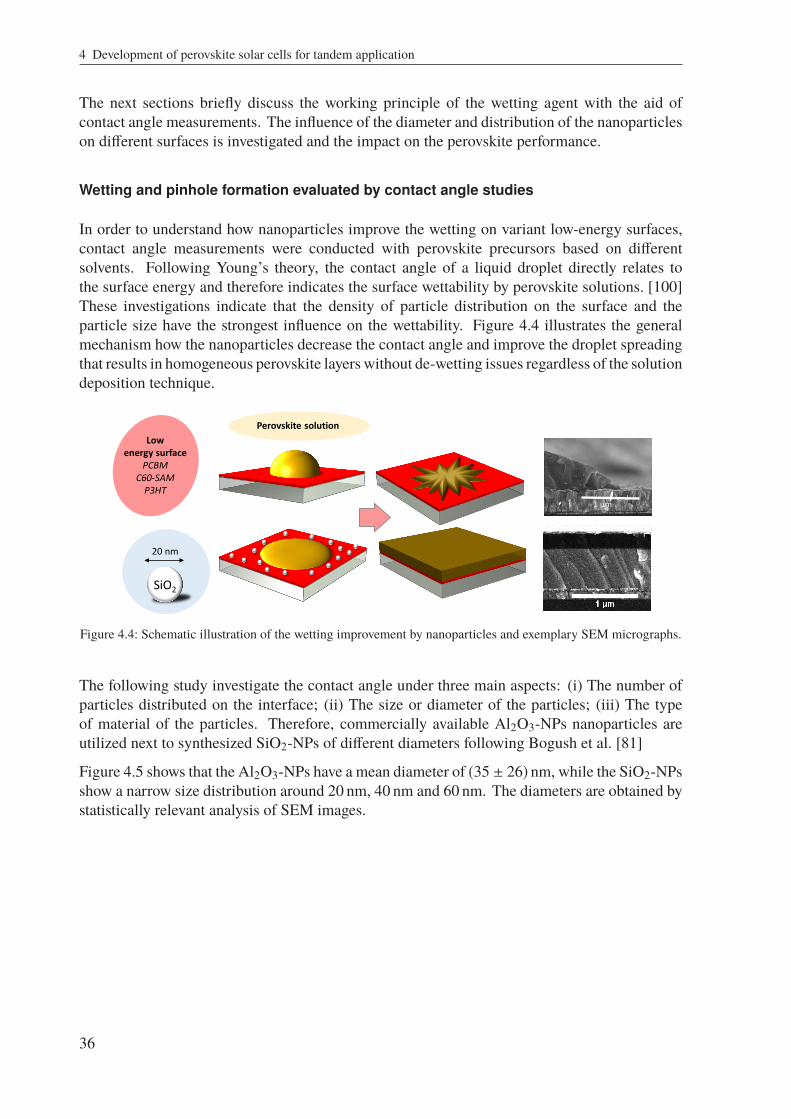
4 Development of perovskite solar cells for tandem application
The next sections briefly discuss the working principle of the wetting agent with the aid ofcontact angle measurements. The influence of the diameter and distribution of the nanoparticleson different surfaces is investigated and the impact on the perovskite performance.
Wetting and pinhole formation evaluated by contact angle studies
In order to understand how nanoparticles improve the wetting on variant low-energy surfaces,contact angle measurements were conducted with perovskite precursors based on differentsolvents. Following Young’s theory, the contact angle of a liquid droplet directly relates tothe surface energy and therefore indicates the surface wettability by perovskite solutions. [100]These investigations indicate that the density of particle distribution on the surface and theparticle size have the strongest influence on the wettability. Figure 4.4 illustrates the generalmechanism how the nanoparticles decrease the contact angle and improve the droplet spreadingthat results in homogeneous perovskite layers without de-wetting issues regardless of the solutiondeposition technique.
Low energy surface
PCBMC60-SAMP3HT
SiO2
20 nm
Perovskite solution
1 µm
Figure 4.4: Schematic illustration of the wetting improvement by nanoparticles and exemplary SEM micrographs.
The following study investigate the contact angle under three main aspects: (i) The number ofparticles distributed on the interface; (ii) The size or diameter of the particles; (iii) The typeof material of the particles. Therefore, commercially available Al2O3-NPs nanoparticles areutilized next to synthesized SiO2-NPs of different diameters following Bogush et al. [81]
Figure 4.5 shows that the Al2O3-NPs have a mean diameter of (35 ± 26) nm, while the SiO2-NPsshow a narrow size distribution around 20 nm, 40 nm and 60 nm. The diameters are obtained bystatistically relevant analysis of SEM images.
36

4.1 Opaque perovskite solar cells
0 10 20 30 40 50 60 70 80 90 100
diameter d (nm)
Count
Al2O3 35 nm
SiO2 40 nm
SiO2 20 nm
SiO2 60 nm
Figure 4.5: Distribution of calculated diameters of different NPs.
To investigate the effect of size and distribution of nanoparticles on the surface, they weredeposited by spin coating from differently diluted alcoholic dispersions. Figure 4.6 shows SEMimages of a fullerene (PCBM) surface and the spatial distribution of nanoparticles depositedfrom differently diluted dispersions. As expected, the surface coverage is strongly dependenton the NP size and the initial concentration. For instance the deposition of Al2O3-NPs from0.2 wt% solution leads to a covered area of about 14 %.
500 nm
500 nm
Al2O3-NPs 35 nm, 0.2 wt%
PCBMWithout NPs
Al2O3-NPs 35 nm, 0.02 wt%
SiO2-NPs 60 nm, 0.2 wt%
SiO2-NPs 40 nm, 0.2 wt%
SiO2-NPs 20 nm, 0.2 wt%
TiO2-NPs <10 nm, 0.2 wt%
SiO2-NPs 5-15 nm, 0.2 wt%
500 nm
500 nm
500 nm 500 nm
5 µm 5 µm
Figure 4.6: SEM micrographs of various nanoparticles on PCBM-surface.
At first, the impact of the number of particles is investigated. Therefore, a series of differentlydiluted Al2O3-NP dispersions is utilized to generate interfaces with different coverage ratios.Following the graphs in Figure 4.7a, different combinations of hydrophobic interlayers (PCBMor C60–SAM) and perovskite precursors based on the solvents DMF, GBL and DMSO revealthe strong decrease of the contact angle with increase of the nanoparticle concentration. Thegraph shows that the initial contact angle is strongly dependent on the type of solvent–interfacecombination. This means that the wetting e.g. of a DMF based solution on a PCBM interface ismuch more difficult, than using a GBL based solution on a less hydrophobic C60–SAM interface.
37

4 Development of perovskite solar cells for tandem application
In all cases, increasing the nanoparticle concentration and overcoming a critical surface coverageleads to contact angle reduction to less than 10° and a change in the droplet wetting behaviour.The perovskite precursor solution then spreads almost perfectly flat on top of the substrate,regardless of the initial hydrophobicity of the interface.
20 nm40 nm60 nmReference
5
10
15
20
25
30
35
40
45
50
55
60
conta
ct
angle
T (
°)SiO2-NP diameter d (nm)
0.001 0.01 0.1
5
10
15
20
25
30
35
40
45
50
55
60
conta
ct
angle
T (
°)
Al2O3-NP concentration c (wt%)
PCBM/NPs/MAPI(DMF)
C60-SAM/NPs/MAPI(DMF)
C60-SAM/NPs/MAPI(GBL)
PCBM/MAPI(DMF)
PCBM/Ethanol/MAPI(DMF)
PCBM/NPs(0.4 wt%)/MAPI(DMF)
PCBM/NPs(0.6 wt%)/MAPI(DMF)
a) b)
Figure 4.7: a) Contact angles of DMF or GBL based perovskite solutions on fullerene interface (PCBM orC60–SAM) covered with Al2O3-NPs from differently concentrated solutions; b) contact angle of aDMF based perovskite solution on PCBM interface covered with differently sized SiO2-NPs.
Secondly, the impact of the size of the NPs is investigated. Figure 4.7b shows, that particles witha smaller diameter lead to a stronger decline of the contact angle. For this study, ethanol baseddispersions with 0.4 and 0.6 wt% concentration of SiO2 nanospheres of diameters of 20, 40 and60 nm (see Figure 4.5) were applied. Reference samples with untreated- and ethanol pre-treatedPCBM surfaces have both high contact angles of about 45°, indicating a weak effect of puresolvent pre-treatment. Alternative solvents pretreatments with DMF, GBL or isopropanol seemto have similarly little influence on the contact angle.
The results indicate that the wetting behaviour is mainly influenced by concentration and sizeof the nanoparticles. The type of material has a lesser impact in this case where two oxidicNPs are applied, both capable of reducing the contact agle dramatically. Here with siliconoxide (SiO2), the contact angle declines below 10° in case of the smallest particles (20 nm)at 0.6 wt% concentration. Notably, the variation of the diameter has a stronger effect on thecontact angle than increasing the concentration. The same relation between contact angle andnanoparticle size is shown by Munshi et al. [101] in a different case study.
The well-established contact angle theories of Wenzel and Cassie predict that the roughness hasa strong influence on the contact angle. They describe also the transitions from the non-wettingCassie state, in which the droplet sits on top of a rough morphology with air trapped underneath,to a wetting Wenzel state, where the droplet completely penetrates the surface. [102,103] In thiscase, a rising number of nanoparticles increases the roughness of the interface and leads to adirect decline of the wetting angle. In consequence, wetting behaviour indicates a Wenzel-likemechanism, at which the high surface energetic oxide particles increase the overall surfaceenergy dominated by the fullerenes and act as capillary features that force the liquid to spreadin between the gaps of the energetically favoured particles. Other fields of research, e.g. thefabrication of solution-processable organic transistors on hydrophobic surfaces, confirmed thevalidity of the Wenzel-like wetting mechanism. [104,105]
38

4.1 Opaque perovskite solar cells
There are two reasons why a decrease of the particle diameter favors the wetting even more. Bykeeping the mass concentration in the precursor dispersion constant, a reduction of the particlediameter leads to a significantly increased particle density at the interface. This can be observedas a higher surface roughness, which generally improves the wetting mechanism. [101,106] Anincreased number of gaps between small particles with a higher surface energy exhibit a strongcapillary force and therefore enable the perovskite solution to spread more easily. Furthermore,this explains why nanoparticles smaller than 20 nm show negative effects on the wetting. Due totheir increased surface energy, the particles agglomerate (see Figure 4.6 TiO2 –NPs) and therebythe capillary action is inhibited by the large distance between the clusters.
Following the results of the contact anglemeasurements, a goodwettability of a typical perovskitesolution on a fullerene interface usually requires a nanoparticle concentration of no more than0.2 wt% at a diameter of 20 nm. Then the contact angle is so low, that a good spreading of thedroplet allows for a complete coverage of the substrate. However, despite good coverage, whendealing with very hydrophobic surfaces like PCBM compared to C60–SAMs, pinhole formationin the perovskite layer is often an additional issue, which is highly critical especially for theupscaling of perovskite solar cells. [107] In order to analyse this effect in more detail, twosubstrates (ITO and FTO) with different surface roughness have been prepared by treating thehydrophobic PCBM interface by a 0.2 wt% Al2O3-NP wetting agent layer to enable full wetting.
Figure 4.8a and c shows the formation of macroscopic pinholes in the crystallized perovskitelayer in the top-view photographs and confocal micrographs after spin coating a MAPI basedperovskite along with a toluene anti solvent step. The first surface ITO/SnO2/PCBM has a lowroughness, which decreases the surface energy, and shows more and larger pinholes in contrastto the second rougher FTO/SnO2/PCBM sample.
500 nm
500 nm
ITOSnO2
PCBMMAPbI3
FTOSnO2
PCBMMAPbI3
PCBM
0.2 wt% ITO
PCBM
PCBM
0.5 wt% ITO
PCBM
0.5 wt%FTOFTO0.2 wt%
c)
a) b)
d)
Ra = 7 nm
Ra = 14 nm
1 cm
1 cm
1 cm
1 cm
Figure 4.8: a-d) demonstration of pinhole defect suppression on different substrates (ITO/SnO2, FTO/SnO2) withPCBM as fullerene layer.
39

4 Development of perovskite solar cells for tandem application
The pinholes form due to de-wetting of the still-wet precursor solution during spin coating priorto the perovskite crystallization. When the addition of toluene induces the phase transition, theshape of the pinhole freezes. Simultaneously, the toluene dissolves and removes the PCBM fromthe pinhole bottom. This example shows how substrate morphology, choice of materials andsolvents can lead to different wetting issues. In both cases however, the pinholes are effectivelysuppressed by increasing the surface energy with the application of a higher concentration ofAl2O3-NPs of 0.5 wt% as shown in Figure 4.8b and d.
Performance of perovskite solar cells employing nanoparticle wetting agent
In order to study the impact of the wetting strategy on the solar cell performance, full devicestacks with variation in type, size and distribution of NPs and fullerene–absorber combinationswere prepared. As described in the previous section, the concentration of the nanoparticleprecursor dispersion coordinates the NP–distribution at the interface after spin coating, whichhas a direct influence on the wetting behaviour. A bad wetting at low concentrations requires amanual spreading of the droplet onto the PCBM interface with the pipette tip. In a setup witha simple MAPI absorber and PCBM fullerene interface (FTO/SnO2/PCBM/Al2O3-NPs/MAPI/Spiro/Au) the concentrations influence on the JV–characteristics was tested (Figure 4.9).
0.02 0.05 0.2 0.5 20.01 0.1 1
8
10
12
14
16
PC
E (
%)
Al2O3-NP concentration (wt%)
reverse scan linear fit 95% confidence band
1000
1020
1040
1060V
OC (
mV
)
18
19
20
21
22
JS
C (
mA
cm
-2)
40
50
60
70
FF
(%
)
-20
0
20
40
FH
YS (
%)
Figure 4.9: JV–characteristics of PSCs (FTO/SnO2/PCBM/Al2O3-NPs/MAPbI3/Spiro/Au) using different concen-trations of Al2O3-NPs as a wetting agent.
Steady average PCE-results between 13 % and 14 % were achieved in all setups, which indicatesthat the inert metal oxide nanoparticles do not take negative effect on the device functionality.Even at a very high concentration of 2.0 wt%, which results to full NP-coverage of the interface,no significant loss in JSC can be observed. This must be attributed to the transparent nature ofthe wide band gap Al2O3-insulator and in consequence very little parasitic absorption.
40
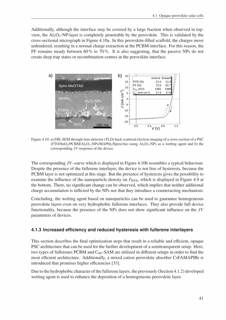
4.1 Opaque perovskite solar cells
Additionally, although the interface may be covered by a large fraction when observed in top-view, the Al2O3-NP-layer is completely penetrable by the perovskite. This is validated by thecross-sectional micrograph in Figure 4.10a. In this perovskite-filled scaffold, the charges moveunhindered, resulting in a normal charge extraction at the PCBM-interface. For this reason, theFF remains steady between 60 % to 70 %. It is also suggesting, that the passive NPs do notcreate deep trap states or recombination centres at the perovskite interface.
a)
250 nm
Spiro-MeOTAD
MAPbI3 Al2O3-NPs
FTO
PCBM
SnO2 0.0 0.4 0.8 1.2
-20
-15
-10
-5
0
5
10
15
20
J (
mA
cm
-2)
V (V)
b)reverse forward
PCE (%) 13.4 11.9
FF (%) 72.6 62.7
VOC (mV) 1065 1068
JSC (mA cm-2) 17.4 17.8
Figure 4.10: a) FIB–SEM through-lens-detector (TLD) back scattered electron imaging of a cross-section of a PSC(FTO/SnO2/PCBM/Al2O3-NPs/MAPbI3/Spiro/Au) using Al2O3-NPs as a wetting agent and b) thecorresponding JV-response of the device.
The corresponding JV–curve which is displayed in Figure 4.10b resembles a typical behaviour.Despite the presence of the fullerene interlayer, the device is not free of hysteresis, because thePCBM layer is not optimized at this stage. But the presence of hysteresis gives the possibility toexamine the influence of the nanoparticle density on FHYS, which is displayed in Figure 4.9 atthe bottom. There, no significant change can be observed, which implies that neither additionalcharge accumulation is inflicted by the NPs nor that they introduce a counteracting mechanism.
Concluding, the wetting agent based on nanoparticles can be used to guarantee homogeneousperovskite layers even on very hydrophobic fullerene interfaces. They also provide full devicefunctionality, because the presence of the NPs does not show significant influence on the JVparameters of devices.
4.1.3 Increased efficiency and reduced hysteresis with fullerene interlayers
This section describes the final optimization steps that result in a reliable and efficient, opaquePSC architecture that can be used for the further development of a semitransparent setup. Here,two types of fullerenes PCBM and C60–SAM are utilized in different setups in order to find themost efficient architecture. Additionally, a mixed cation perovskite absorber CsFAMAPIBr isintroduced that promises higher efficiencies [33].
Due to the hydrophobic character of the fullerene layers, the previously (Section 4.1.2) developedwetting agent is used to enhance the deposition of a homogeneous perovskite layer.
41

4 Development of perovskite solar cells for tandem application
Fullerenes (PCBM and C60-SAM) in MAPI based solar cells
Next to PCBM, the following experiment utilizes C60–SAM, which has selective side groupsthat preferably bond to the oxide surface of the ETL. In consequence a very thin and dense layer,referred to as a monolayer, forms at the interface. Devices with ITO/c-SnO2/PCBMand ITO/c-SnO2/C60-SAM are fabricated in order to evaluate the influence of both approaches.
The performance of the corresponding PSCs benefits from both approaches. Figure 4.11 a–c) compares the JV– and MPP–data of the ITO/c-SnO2 reference device without fullereneinterlayer and the setups with either PCBM or C60–SAM. Obviously, both fullerene typeseffectively suppress the hysteresis that is strongly pronounced in the reference device. Thehysteretic difference of FF and VOC of between rvs and fwd scan is equalized with application ofthe fullerenes. Moreover, the absolute VOC–value is improved by 30 mV to 40 mV. As a resultof the hysteresis-free behaviour and the increased voltage, the stable power output at MPP isimproved from 12.0 % to 13.5 % and 15.1 % for PCBM and C60–SAM respectively.
0.0 0.4 0.8 1.2
-20
-15
-10
-5
0
5
J (
mA
cm
-2)
V (V)
0 10 20 30
10
13
16
t (s)
PC
E (
%)
0.0 0.4 0.8 1.2
-20
-15
-10
-5
0
5
J (
mA
cm
-2)
V (V)
0 10 20 30
10
13
16
t (s)
PC
E (
%)
0.0 0.4 0.8 1.2
-20
-15
-10
-5
0
5
J (
mA
cm
-2)
V (V)
0 10 20 30
10
13
16
t (s)
PC
E (
%)
a) b) c)
12.0%
13.5% 15.1%
c-SnO2rvs fwd
PCE (%) 13.5 9.6
FF (%) 69.6 56.0
VOC (mV) 1067 939
JSC (mA cm-2) 18.2 18.2
c-SnO2/PCBM rvs fwd
PCE (%) 13.0 12.9
FF (%) 69.0 68.8
VOC (mV) 1092 1083
JSC (mA cm-2) 17.3 17.2
c-SnO2/C60-SAM rvs fwd
PCE (%) 14.1 14.2
FF (%) 69.8 69.8
VOC (mV) 1104 1109
JSC (mA cm-2) 18.4 18.3
Figure 4.11: JV–characteristics and MPP responses of MAPI–based devices a) without fullerene interlayer, b) withPCBM and c) with C60–SAM.
Similar to the previously discussed devices employing FTO, the PCBM–based cells of this studyexperience a JSC loss of −1 mA cm−2 compared to the reference and the C60–SAM device. Thisis most likely related to parasitic absorption by comparably thick PCBM layer. Here, a spinparameter set1 was chosen to create a PCBM-film with a thickness 30 nm to 40 nm, which moreeffectively suppresses hysteresis than thinner layers.
Conclusively, in this setup with simple MAPI–absorber the combination of ITO/c-SnO2/C60-SAM as an ETL outperforms ITO/c-SnO2/PCBM. Reducing the fullerene film thickness provedto be a decisive factor for a high current density. Moreover, C60–SAM has an advance overPCBM regarding its wetting behaviour, because of a higher polarity.
Fullerenes (PCBM and C60-SAM) in mixed cation CsFAMAPIBr solar cells
Utilizing the mixed cation perovskite absorber CsFAMAPIBr instead of the simple MAPI ap-proach promises a higher efficiency, reproducibility, and stability [33]. But after the applicationof this absorber in a similar setup with ITO and compact c-SnO2 a pronounced hysteresis in theirJV–responses is observable. The results are displayed in Figure 4.12. In all scans a significant1 rotational frequency ( frot)= 2000 min−1; cPCBM = 20 mg ml−1; chlorobenzene (CB)
42
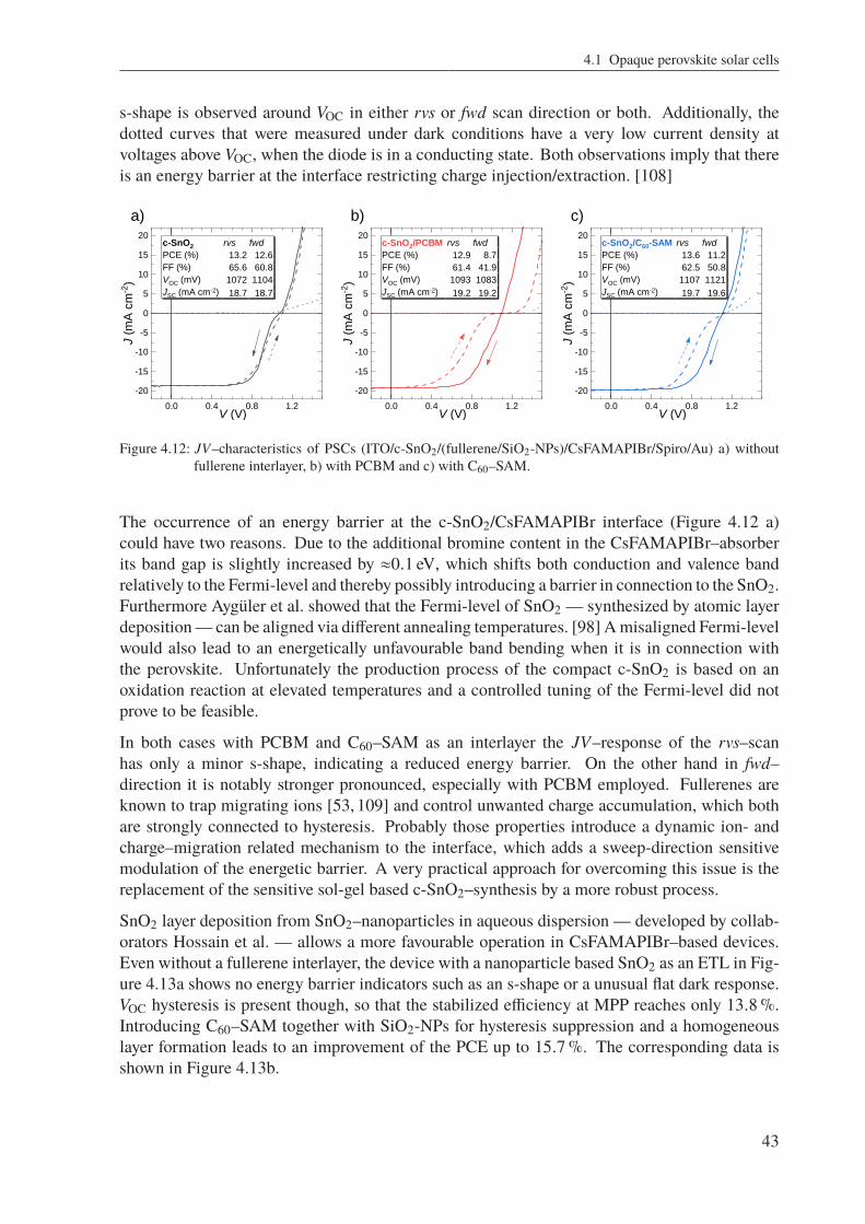
4.1 Opaque perovskite solar cells
s-shape is observed around VOC in either rvs or fwd scan direction or both. Additionally, thedotted curves that were measured under dark conditions have a very low current density atvoltages above VOC, when the diode is in a conducting state. Both observations imply that thereis an energy barrier at the interface restricting charge injection/extraction. [108]
0.0 0.4 0.8 1.2
-20
-15
-10
-5
0
5
10
15
20
J (
mA
cm
-2)
V (V)0.0 0.4 0.8 1.2
-20
-15
-10
-5
0
5
10
15
20
J (
mA
cm
-2)
V (V)0.0 0.4 0.8 1.2
-20
-15
-10
-5
0
5
10
15
20 c-SnO2
SnO2-NPs
J (
mA
cm
-2)
V (V)
c-SnO2 rvs fwd
PCE (%) 13.2 12.6
FF (%) 65.6 60.8
VOC (mV) 1072 1104
JSC (mA cm-2) 18.7 18.7
c-SnO2/PCBM rvs fwd
PCE (%) 12.9 8.7
FF (%) 61.4 41.9
VOC (mV) 1093 1083
JSC (mA cm-2) 19.2 19.2
c-SnO2/C60-SAM rvs fwd
PCE (%) 13.6 11.2
FF (%) 62.5 50.8
VOC (mV) 1107 1121
JSC (mA cm-2) 19.7 19.6
a) b) c)
Figure 4.12: JV–characteristics of PSCs (ITO/c-SnO2/(fullerene/SiO2-NPs)/CsFAMAPIBr/Spiro/Au) a) withoutfullerene interlayer, b) with PCBM and c) with C60–SAM.
The occurrence of an energy barrier at the c-SnO2/CsFAMAPIBr interface (Figure 4.12 a)could have two reasons. Due to the additional bromine content in the CsFAMAPIBr–absorberits band gap is slightly increased by ≈0.1 eV, which shifts both conduction and valence bandrelatively to the Fermi-level and thereby possibly introducing a barrier in connection to the SnO2.Furthermore Aygüler et al. showed that the Fermi-level of SnO2 — synthesized by atomic layerdeposition— can be aligned via different annealing temperatures. [98] Amisaligned Fermi-levelwould also lead to an energetically unfavourable band bending when it is in connection withthe perovskite. Unfortunately the production process of the compact c-SnO2 is based on anoxidation reaction at elevated temperatures and a controlled tuning of the Fermi-level did notprove to be feasible.
In both cases with PCBM and C60–SAM as an interlayer the JV–response of the rvs–scanhas only a minor s-shape, indicating a reduced energy barrier. On the other hand in fwd–direction it is notably stronger pronounced, especially with PCBM employed. Fullerenes areknown to trap migrating ions [53, 109] and control unwanted charge accumulation, which bothare strongly connected to hysteresis. Probably those properties introduce a dynamic ion- andcharge–migration related mechanism to the interface, which adds a sweep-direction sensitivemodulation of the energetic barrier. A very practical approach for overcoming this issue is thereplacement of the sensitive sol-gel based c-SnO2–synthesis by a more robust process.
SnO2 layer deposition from SnO2–nanoparticles in aqueous dispersion — developed by collab-orators Hossain et al. — allows a more favourable operation in CsFAMAPIBr–based devices.Even without a fullerene interlayer, the device with a nanoparticle based SnO2 as an ETL in Fig-ure 4.13a shows no energy barrier indicators such as an s-shape or a unusual flat dark response.VOC hysteresis is present though, so that the stabilized efficiency at MPP reaches only 13.8 %.Introducing C60–SAM together with SiO2-NPs for hysteresis suppression and a homogeneouslayer formation leads to an improvement of the PCE up to 15.7 %. The corresponding data isshown in Figure 4.13b.
43

4 Development of perovskite solar cells for tandem application
0.0 0.4 0.8 1.2
-20
-15
-10
-5
0
5
J (
mA
cm
-2)
V (V)
0 10 20 30
10
13
16
t (s)
PC
E (
%)
0.0 0.4 0.8 1.2
-20
-15
-10
-5
0
5
J (
mA
cm
-2)
V (V)
0 10 20 30
10
13
16
t (s)
PC
E (
%)
a) b)
15.7%13.8%
SnO2-NP rvs fwd
PCE (%) 14.9 13.2
FF (%) 73.3 68.5
VOC (mV) 1085 1031
JSC (mA cm-2) 18.7 18.7
SnO2-NP/
C60-SAM rvs fwd
PCE (%) 15.3 15.2
FF (%) 72.5 74.6
VOC (mV) 1108 1078
JSC (mA cm-2) 19.0 19.0
Figure 4.13: JV–characteristics of a) PSCs ITO/SnO2-NP/CsFAMAPIBr/Spiro/Au and b) ITO/SnO2-NP/C60-SAM/SiO2-NPsCsFAMAPIBr/Spiro/Au.
This section demonstrates how engineering the morphology and the ETL interface of the solarcells can lead to significantly increased efficiencies. With the introduction of fullerene interlayersat this interface, the hysteresis of the devices could be reduced to a minimum. The developedwetting agent based on NPs enables a reproducible deposition of the perovskite layer preventingthe formation of de-wetting defects. These optimization steps combined with a more capableCsFAMAPIBr perovskite lead to an even higher performance of the PSC.
Concluding, the ETL interface at the front side of the devices is successfully optimized. Thisnew base process is utilized for the upcoming integration of transparent electrodes at the rearinterface. The development of suitable transparent contact materials for this purpose is part ofthe next section.
4.2 Sputter-deposition of suitable transparent conductive oxides astransparent electrodes
The following sputter depositions were conducted by Tim Helder under guidance of the authorand the results reflect the main findings of his master thesis. [110]
For the transition from opaque to semitransparent PSCs, the metal rear electrode needs to bereplaced by a transparent one. Considering the sensitive PSC layers, this requires a depositionprocess with a low thermal impact. Additionally, for implementation in a tandem cell, allelectrodes must have a high overall transmittance, but especially a low parasitic absorption inthe NIR range is demanded. Hence, the unfavourable front electrodes ITO or FTO should bealso exchanged, as they only offer a good transparency in the visible range.
IO:H and IZO have been identified in Section 2.3 as suitable electrode materials promising tofulfil these high demands. In the following, the parameters for sputter deposition of these TCOsare evaluated, targeting to match the demanded properties. Thereby, all optimizations of theprocesses are carried out on glass substrates, while the implementation of the TCO layer intoPSC devices follows later on in Section 4.3.
44

4.2 Sputter-deposition of suitable transparent conductive oxides as transparent electrodes
At first, Section 4.2.1 discusses the sputter deposition of IZO at ambient temperature conditionsfor low thermal impact. Focusing on controlling the doping level and the thickness, the aim isto find the optimal process for depositing a suitable rear electrode.
Subsequently, Section 4.2.2 discusses the sputter deposition and annealing of IO:H. A spe-cial focus lies on the post deposition recrystallization, which allows for extraordinary opticalproperties and makes IO:H the most promising material as a front electrode.
Finally, the new materials are compared to the traditional electrode layers FTO, ITO and ZAO.
4.2.1 Amorphous indium zinc oxide deposited with low thermal impact
The tuning of the optical properties of the amorphous IZO layers is accomplished only byvariations of the sputter parameters, since is deposited from a target with a fixed In2O3:ZnOcomposition of 9:1 and the whole process is restricted to ambient temperature conditions. Thenext section discusses the influence of the pressure and the oxygen content on the doping leveland the corresponding electrical and optical properties. Thereafter, the demanded electrodeproperties are fine-adjusted by means of controlling the layer thickness.
Optimization of doping level in IZO by variation of the pressure and oxygen content
The doping level of amorphous IZO films is controlled mainly by the partial pressure of oxygenin the sputter gas. [62, 64] With control over the doping level, the desired optical and electricalproperties can be engineered. This section is about to evaluate the process parameters neededfor a highly conductive and yet transmissive IZO electrode.
A series of IZO layers was prepared via DC sputter deposition varying the O2 content from 1 % to3 % at different process pressures of 10 µbar and 15 µbar. Figure 4.14a shows the results of Hallmeasurements in terms of resistivity (ρ), charge carrier mobility (µ) and electron density (Ne)with respect to the O2 content. Ne decreases from high values of about 6 × 1020 cm−3 to valuesbelow 1 × 1020 cm−3 with increasing oxygen content, due to a decreased doping density byoxygen vacancies in the layer. [65]
Reasoned by the reduction of the vacancies, the scattering at ionized impurities is reduced, henceµ increases inversely to Ne. Additionally, abundant oxygen in the sputter gas prevents metalinclusions and metal pairs (In–In and In–ZnO) as further scattering centres.
At an oxygen content of 1.2 % and a pressure of 15 µbar ρ reaches a minimum with a moderateNe and a high µ as labelled in the graph, which is comparable to the state of the art. [61, 62,65]
45
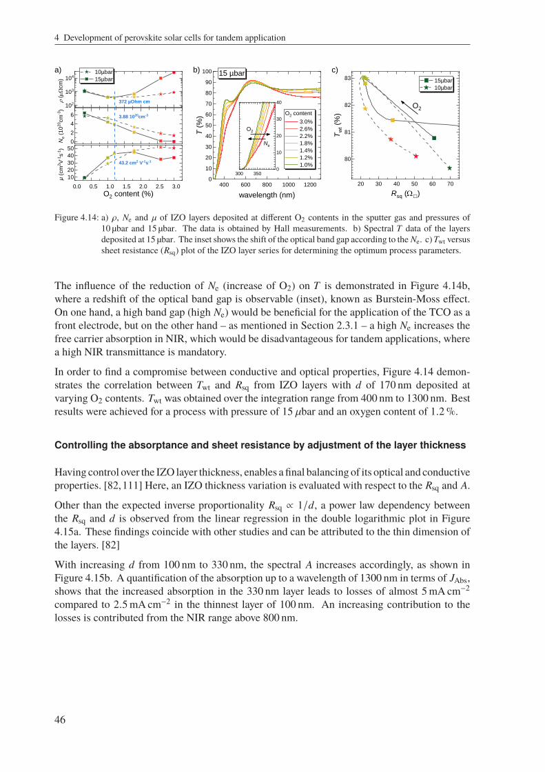
4 Development of perovskite solar cells for tandem application
102
103
104
0
2
4
6
0.0 0.5 1.0 1.5 2.0 2.5 3.0
10
20
30
40
50
43.2 cm2 V-1s-1
3.88 1020cm-3
r (
mW
cm
)
10µbar
15µbar
372 µOhm cm
Ne (
10
20cm
-3)
µ (
cm
2V
-1s
-1)
O2 content (%)
400 600 800 1000 12000
10
20
30
40
50
60
70
80
90
100
Ne
T (
%)
wavelength (nm)
O2 content
3.0%
2.6%
2.2%
1.8%
1.4%
1.2%
1.0%
O2
15 µbar
300 3500
10
20
30
40
20 30 40 50 60 70
80
81
82
83 15µbar
10µbar
Tw
t (%
)
Rsq (W")
O2
a) b) c)
Figure 4.14: a) ρ, Ne and µ of IZO layers deposited at different O2 contents in the sputter gas and pressures of10 µbar and 15 µbar. The data is obtained by Hall measurements. b) Spectral T data of the layersdeposited at 15 µbar. The inset shows the shift of the optical band gap according to the Ne. c)Twt versussheet resistance (Rsq) plot of the IZO layer series for determining the optimum process parameters.
The influence of the reduction of Ne (increase of O2) on T is demonstrated in Figure 4.14b,where a redshift of the optical band gap is observable (inset), known as Burstein-Moss effect.On one hand, a high band gap (high Ne) would be beneficial for the application of the TCO as afront electrode, but on the other hand – as mentioned in Section 2.3.1 – a high Ne increases thefree carrier absorption in NIR, which would be disadvantageous for tandem applications, wherea high NIR transmittance is mandatory.
In order to find a compromise between conductive and optical properties, Figure 4.14 demon-strates the correlation between Twt and Rsq from IZO layers with d of 170 nm deposited atvarying O2 contents. Twt was obtained over the integration range from 400 nm to 1300 nm. Bestresults were achieved for a process with pressure of 15 µbar and an oxygen content of 1.2 %.
Controlling the absorptance and sheet resistance by adjustment of the layer thickness
Having control over the IZO layer thickness, enables a final balancing of its optical and conductiveproperties. [82,111] Here, an IZO thickness variation is evaluated with respect to the Rsq and A.
Other than the expected inverse proportionality Rsq ∝ 1/d, a power law dependency betweenthe Rsq and d is observed from the linear regression in the double logarithmic plot in Figure4.15a. These findings coincide with other studies and can be attributed to the thin dimension ofthe layers. [82]
With increasing d from 100 nm to 330 nm, the spectral A increases accordingly, as shown inFigure 4.15b. A quantification of the absorption up to a wavelength of 1300 nm in terms of JAbs,shows that the increased absorption in the 330 nm layer leads to losses of almost 5 mA cm−2
compared to 2.5 mA cm−2 in the thinnest layer of 100 nm. An increasing contribution to thelosses is contributed from the NIR range above 800 nm.
46

4.2 Sputter-deposition of suitable transparent conductive oxides as transparent electrodes
a) b) c)
40 60 80 200 400 6001004
6
8
20
40
60
80
200
10
100
Rsq (W
)
d (nm)
0
10
20
30
40
50
400 600 800 1000 12000
1
2
3
4d
A (
%)
d
wavelength (nm)
JA
bs (
mA
cm
-2)
330 nm
280 nm
200 nm
170 nm
100 nm
10 20 30 405
6
7
8
9
10
11
100 nm
170 nm
200 nm
280 nm
330 nm
Aw
t (%
)
Rsq (W)
Figure 4.15: a) Double log plot of Rsq versus d for different IZO layers deposited at 1.2 % O2 and 15 µbar indicatingan inverse proportionality. b) Spectral A and JAbs data of equivalent layers with d from 100 nm to330 nm. c) Awt versus Rsq plot of the IZO layer series for determining the optimum d.
The correlation between the Rsq and theweighted average absorptance (Awt) (300 nm to 1300 nm)in Figure 4.15c indicates that a suitable compromise is matched for combinations of low A andRsq. From the tested data set the combination with a layer thickness of 170 nm, an Awt of 6.3 %and a Rsq of 22Ω is chosen to suit the demanded properties of a rear electrode for PSCs in thebest way.
4.2.2 Hydrogen doped indium oxide with ultra-low absorption
In contrast to amorphous IZO, pure In2O3 grows in a crystalline form during sputter deposition.It is due to the incorporation of hydrogen in the crystal lattice during that process, that IO:Hcan be deposited as an amorphous layer, which in turn allows for a subsequent controlledannealing step in order to crystallize it. The prerequisites and consequences of this method willbe discussed in the following. Subsequently, the doping level of the IO:H layers is adjustedin order to optimise the optical and electrical properties for the targeted application as a frontelectrode on the glass superstrate of PSCs.
Post deposition crystallization of hydrogenated, amorphously grown Indium oxidelayers
The outstanding conductive and optical properties of IO:H rely on the controlled post-deposition-crystallisation (PDC) from a formerly amorphous hydrogenated indium oxide (a-IO:H) film.By this, the Ne is reduced, which in turn is compensated by a high µ to maintain sufficientconductivity. [15, 16] The amorphous growth, most likely induced by hydroxylation, [112]demands sufficient hydrogen doping of the pure In2O3 during the sputter deposition, which istraditionally accomplished by water vapor (H2O) injection into the sputter gas (Ar). [15] Here,argon and hydrogen (Ar/H2) are used as a mass flow controllable reactive gas component forinitiating the hydroxylation of the IO:H layers.
47

4 Development of perovskite solar cells for tandem application
The H2 induced amorphous growth of a-IO:H is investigated by XRD. The resulting patternsin Figure 4.16a reveal that for low amounts of hydrogen <2.0 % H2 the as-deposited layers(dashed lines) grow already in a polycrystalline (PC) phase with a preferential (222) orientation.The preferentially oriented crystalline character of the layer remains throughout the subsequentannealing step (solid lines), visible in the dominant intensity of the (222) peak ∗∗ and relatedcrystallographic reflections (332) and (444).
As expected, raising the H2-content to >2.8 % leads to completely amorphous growth andallows for the aforementioned controlled PDC. After the transformation from amorphous tocrystalline, further dominant reflections (+) of the indium oxide structure are apparent, indicatingno preferential lattice orientation. A less intense signal of the (222) peak (∗) supports theobservation.
Furthermore, at low amounts of hydrogen (H2), a shift of the peak positions towards lowerangles is observed, if compared to the reference structure data of In2O3, which is indicatedby the vertical lines. [113] In contrast, the post-deposition-crystallised hydrogenated indiumoxide (PDC–IO:H) layers do not show this effect. The shift may be reasoned by lattice strainsoriginating from crystal defects, which are effectively outmanoeuvred by the PDC approach.This effect is evaluated by GIXRD in more detail later in this Section.
400 600 800 1000 12000
10
20
30
40
50
Absorp
tance (
%)
Wavelength (nm)
As deposited
Annealed
0.0% H2
1.0% H2
2.0% H2
2.8% H2
3.5% H2
350 4000
10
20
30
H2
H2
PDC
amorphous
a) b)
c)
0
2
4
6
1.0 1.5 2.0 2.5 3.0 3.5
20
40
60
80
100
20
50
200
500
10
100
polycrystalline
PDC
Ne (
10
20cm
-3)
PDC
µ (
cm
2V
-1s
-1)
H2 content (%)
As deposited
AnnealedR
sq (
W)
amorphous
25 30 35 40 45 50 55 60 65 70
crystallisedpost-deposition-
polycrystalline
polycrystalline As deposited Annealed
PDC
polycrystalline
polycrystalline
*
#
amorphous
+
#
#
#
#
◊
◊
◊
◊
◊
+
(444
)
(622
)
(440
)
(134
)
(332
)
(400
)
(222
)
(211
)
##
##
+
**
**
**
*
*
**
2.8% H2
3.5% H2
2.0% H2
1.0% H2
log I
nte
nsity
Diffracted Angle 2q (°)
0.0% H2
**
+
##
+
++
+
PDC
amorphous
PDC
semi-amorphous
Figure 4.16: a) XRD patterns of IO:H layers deposited at different H2 contents in the sputter atmosphere. Thedashed lines represent the as deposited layers, while the solid lines represent data from the same layersafter annealing at 200 C for 30 min. The vertical lines indicate the pure In2O3 structure. [113] b) Rsq,Ne and µ data and c) spectral A data of equivalent layers. The inset shows the shift of the optical bandgap.
48
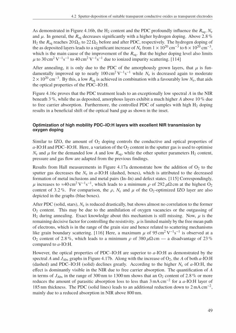
4.2 Sputter-deposition of suitable transparent conductive oxides as transparent electrodes
As demonstrated in Figure 4.16b, the H2 content and the PDC profoundly influence the Rsq, Neand µ. In general, the Rsq decreases significantly with a higher hydrogen doping. Above 2.8 %H2 the Rsq reaches 20Ω to 22Ω before and after PDC, respectively. The hydrogen doping ofthe as deposited layers leads to a significant increase of Ne from 1 × 1020 cm−3 to 6 × 1020 cm−3,which is the main cause of the improvement of the Rsq. But the higher doping level also limitsµ to 30 cm2 V−1s−1 to 40 cm2 V−1s−1 due to ionized impurity scattering. [114]
After annealing, it is only due to the PDC of the amorphously grown layers, that µ is fun-damentally improved up to nearly 100 cm2 V−1s−1 while Ne is decreased again to moderate2 × 1020 cm−3. By this, a low Rsq is achieved in combination with a favourably low Ne, that aidsthe optical properties of the PDC–IO:H.
Figure 4.16c proves that the PDC treatment leads to an exceptionally low spectral A in the NIRbeneath 3 %, while the as deposited, amorphous layers exhibit a much higher A above 10 % dueto free carrier absorption. Furthermore, the controlled PDC of samples with high H2 dopingresults in a beneficial shift of the optical band gap as shown in the inset.
Optimization of high mobility PDC–IO:H layers with excellent NIR transmission byoxygen doping
Similar to IZO, the amount of O2 doping controls the conductive and optical properties ofa-IO:H and PDC–IO:H. Here, a variation of the O2 content in the sputter gas is used to optimiseNe and µ for the demanded low A and low Rsq, while the other sputter parameters H2 content,pressure and gas flow are adapted from the previous findings.
Results from Hall measurements in Figure 4.17a demonstrate how the addition of O2 to thesputter gas decreases the Ne in a-IO:H (dashed, boxes), which is attributed to the decreasedformation of metal inclusions and metal pairs (In–In) and defect states. [115] Correspondingly,µ increases to ≈40 cm2 V−1s−1, which leads to a minimum ρ of 292 µΩ cm at the highest O2content of 3.2 %. For comparison, the ρ, Ne and µ of the O2-optimized IZO layer are alsodepicted in the graphs (blue boxes).
After PDC (solid, stars), Ne is reduced drastically, but shows almost no correlation to the formerO2 content. This may be due to the annihilation of oxygen vacancies or the outgassing ofH2 during annealing. Exact knowledge about this mechanism is still missing. Now, µ is theremaining decisive factor for controlling the resistivity. µ is limited mainly by the free mean pathof electrons, which is in the range of the grain size and hence related to scattering mechanismslike grain boundary scattering. [116] Here, a maximum µ of 95 cm2 V−1s−1 is observed at aO2 content of 2.8 %, which leads to a minimum ρ of 380 µΩ cm — a disadvantage of 23 %compared to a-IO:H.
However, the optical properties of PDC–IO:H are superior to a-IO:H as demonstrated by thespectral A and JAbs graphs in Figure 4.17b. Along with the increase of O2, the A of both a-IO:H(dashed) and PDC–IO:H (solid) declines greatly. According to the higher Ne of a-IO:H, theeffect is dominantly visible in the NIR due to free carrier absorption. The quantification of Ain terms of JAbs in the range of 300 nm to 1300 nm shows that an O2 content of 2.8 % or morereduces the amount of parasitic absorption loss to less than 3 mA cm−2 for a a-IO:H layer of185 nm thickness. The PDC (solid lines) leads to an additional reduction down to 2 mA cm−2,mainly due to a reduced absorption in NIR above 800 nm.
49
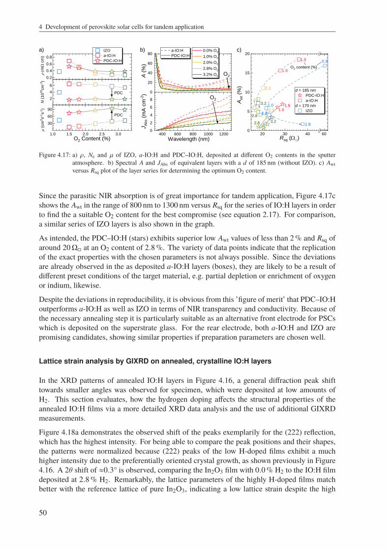
4 Development of perovskite solar cells for tandem application
0
20
40
60
80
400 600 800 1000 12000
2
4
6
8 O2
A (
%)
0.0% O2
1.0% O2
2.0% O2
2.8% O2
3.2% O2
a-IO:H
PDC-IO:H
O2
JA
bs (
mA
cm
-2)
Wavelength (nm)20 30 40 60
0
5
10
15
20
1.51.82.3
2.8 3.2
1.5
1.8
2.3
2.8
3.2
0.3
1.0
1.2
1.8
d = 185 nm
PDC-IO:H
a-IO:H
d = 170 nm
IZO
Aw
t (%
)
Rsq (W)
O2 content (%)
a) b) c)
0.2
0.4
0.6
0.8
2
4
6
1.0 1.5 2.0 2.5 3.0
30
60
90
r (
mW
cm
)
IZO
a-IO:H
PDC-IO:H
PDC
N (
10
20cm
-3)
PDC
m (
cm
2V
-1s
-1)
O2 Content (%)
Figure 4.17: a) ρ, Ne and µ of IZO, a-IO:H and PDC–IO:H, deposited at different O2 contents in the sputteratmosphere. b) Spectral A and JAbs of equivalent layers with a d of 185 nm (without IZO). c) Awtversus Rsq plot of the layer series for determining the optimum O2 content.
Since the parasitic NIR absorption is of great importance for tandem application, Figure 4.17cshows the Awt in the range of 800 nm to 1300 nm versus Rsq for the series of IO:H layers in orderto find the a suitable O2 content for the best compromise (see equation 2.17). For comparison,a similar series of IZO layers is also shown in the graph.
As intended, the PDC–IO:H (stars) exhibits superior low Awt values of less than 2 % and Rsq ofaround 20Ω at an O2 content of 2.8 %. The variety of data points indicate that the replicationof the exact properties with the chosen parameters is not always possible. Since the deviationsare already observed in the as deposited a-IO:H layers (boxes), they are likely to be a result ofdifferent preset conditions of the target material, e.g. partial depletion or enrichment of oxygenor indium, likewise.
Despite the deviations in reproducibility, it is obvious from this ’figure of merit’ that PDC–IO:Houtperforms a-IO:H as well as IZO in terms of NIR transparency and conductivity. Because ofthe necessary annealing step it is particularly suitable as an alternative front electrode for PSCswhich is deposited on the superstrate glass. For the rear electrode, both a-IO:H and IZO arepromising candidates, showing similar properties if preparation parameters are chosen well.
Lattice strain analysis by GIXRD on annealed, crystalline IO:H layers
In the XRD patterns of annealed IO:H layers in Figure 4.16, a general diffraction peak shifttowards smaller angles was observed for specimen, which were deposited at low amounts ofH2. This section evaluates, how the hydrogen doping affects the structural properties of theannealed IO:H films via a more detailed XRD data analysis and the use of additional GIXRDmeasurements.
Figure 4.18a demonstrates the observed shift of the peaks exemplarily for the (222) reflection,which has the highest intensity. For being able to compare the peak positions and their shapes,the patterns were normalized because (222) peaks of the low H-doped films exhibit a muchhigher intensity due to the preferentially oriented crystal growth, as shown previously in Figure4.16. A 2θ shift of ≈0.3° is observed, comparing the In2O3 film with 0.0 % H2 to the IO:H filmdeposited at 2.8 % H2. Remarkably, the lattice parameters of the highly H-doped films matchbetter with the reference lattice of pure In2O3, indicating a low lattice strain despite the high
50

4.2 Sputter-deposition of suitable transparent conductive oxides as transparent electrodes
hydrogen doping. This may be due to the out-gassing of H2 during the PDC of the amorphouslayers in the annealing step. The low H2 samples, which grow already in a polycrystallineform during deposition, do not exhibit a significant phase change during annealing and the peakpositions remain shifted. The shift towards lower angles indicates a de-compressional strain onthe lattice with increased interatomic distances in the unit cell.
0.0 0.1 0.2 0.3 0.4 0.5 0.6
0.0
0.1
0.2
0.3
0.4
0.5
0.6
0.7
0.8
0.0% H2
1.0% H2
2.0% H2
2.8% H2
Si reference
FW
HM
str
uct*
cos(q
)
sin(q)
e
a) b)
29.6 29.8 30.0 30.2 30.4 30.6 30.8 31.0
0.0% H2
1.0% H2
2.0% H2
2.8% H2
(222)N
orm
alis
ed I
nte
nsity
Diffracted Angle 2q (°)
H2
Figure 4.18: a) Shift of the (222) diffraction peak (normalized) in the XRD patterns of annealed IO:H films that weresputter deposited at different H2 gas contents. In addition to the peak shift, the variation in the FWHMindicates a structure related broadening. Similar observations are made for the other reflections overthe full scan range (compare Figure 4.16a). b) Williamson-Hall plot for the same films for evaluationof the structural diffraction peak broadening (FWHMstruct) of all peaks that are distinguishable frombackground and neighbour peaks. The regressions reflect cases where only microstrain contributes tothe broadening at the absence of crystallite size induced broadening (y intercept = 0). Then, the slopeof the regression relates to the lattice strain d/dx = ε induced peak broadening, following equation2.21. Reference data from a polycrystalline Si sample shows neither crystallite size nor microstrainbroadening.
Additionally, the films with 2.0 % and 2.8 % H2 show a narrower FWHM compared to the otherfilms. The broadest peak is observed for the 1.0 % H2 specimen. A peak broadening generallyindicates either a non-uniform influence of microstrain – caused by defects such as dislocationsor antiphase grain boundaries – or contribution of nanometre sized crystallites (compare Section2.5).
With the aid of a Williamson-Hall plot, the different contribution to the peak broadeningcan be distinguished from another following equation 2.21. Therefore, the measured FWHMof all peaks of the specimens are corrected by the instrumental contribution via a standardreferencemeasurement with the same scan parameters. The corrected values are called structuraldiffraction peak broadening (FWHMstruct). Figure 4.18b depicts the resulting Williamson-Hallplot for the different IO:H specimen and a polycrystalline silicon reference sample.
For fitting the regressions in Figure 4.18b, it is assumed that only microstrain contributes to theFWHMstruct:
FWHMstruct · cosθ =KλL︸︷︷︸
y intercept=0
+ 4ε · sinθ︸ ︷︷ ︸microstrain
(4.1)
51

4 Development of perovskite solar cells for tandem application
If crystallite size term is included, the residual of the fit does not change significantly, whichindicates that crystallite size broadening is insignificant in these measurements. Comparing theslopes of the regressions, which directly correlate to themicrostrain ε , no strain is observed for thereference Si specimen, but the IO:H samples all show a significant amount of microstrain. Thehighest microstrain is present in the sample deposited at 1.0 % H2, but due to the preferentiallyoriented crystals, only a few diffraction peaks are visible, which reduces the precision of the fit.All microstrain values that are obtained from the Williamson-Hall plot are listed in Table 4.1.
H2 content Microstrain ε(%) (%)
0.0 0.293 ± 0.0111.0 0.314 ± 0.1922.0 0.135 ± 0.0052.8 0.138 ± 0.004
Table 4.1: Results of the microstrain ε evaluation from the Williamson-Hall plot in Figure 4.18 for annealed IO:Hsamples which were sputter deposited at different H2 sputter gas concentrations.
So far, the strain analysis was based on the XRD data that was obtained from scans in theBragg-Brentano geometry, which is a focused setup with a high penetration depth of the x-raysinto the material. In case of the thin IO:H layers with a thickness of about 180 nm, the beamspetrate the full depth of the film. If possibly different In2O3 phases are apparent, the diffractedpatterns contain only the averaged information of the phases.
As a matter of fact, Muydinov et al. have already reported such different phases in IO:Hlayers with different morphological and electrical properties. [66] Hence, the following GIXRDmeasurements are designed to evaluate, if the observed microstrain of these specimens alsooriginates from local phase differences, e.g. strains at the front surface or at the rear interface onthe glass substrate.
Therefore, a series of GIXRD scans was performed at different ωs ranging from 0.1° to 3° foreach specimen. Thereby, the penetration depth of the x-rays into the material increases with ωas demonstrated in Figure 4.19 for a pure In2O3 layer following equation 2.22. It shows that theincident beam penetrates only the first few nanometres of the layer surface at low incident anglesof 0.1° to 0.3° below ωc. With higher angles, the penetration depth increases and reaches thefull layer thickness of the specimen at about 1.5°. Since the diffracted beammust travel a secondtime through the layer, the actual information depth is lower than the penetration depth. [79]
52
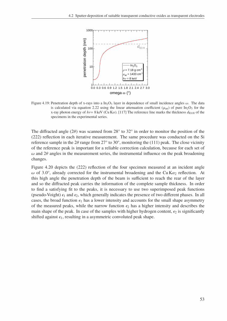
4.2 Sputter-deposition of suitable transparent conductive oxides as transparent electrodes
0.0 0.3 0.6 0.9 1.2 1.5 1.8 2.1 2.4 2.7 3.01
10
100
1000
dIO:H
In2O3
r = 7.18 g cm-3
matt = 1433 cm-1
hn = 8 keV
penetr
atio
n d
epth
(nm
)
omega w (°)
Figure 4.19: Penetration depth of x-rays into a In2O3 layer in dependence of small incidence angles ω. The datais calculated via equation 2.22 using the linear attenuation coefficient (µatt) of pure In2O3 for thex-ray photon energy of hν= 8 keV (CuKα). [117] The reference line marks the thickness dIO:H of thespecimens in the experimental series.
The diffracted angle (2θ) was scanned from 28° to 32° in order to monitor the position of the(222) reflection in each iterative measurement. The same procedure was conducted on the Sireference sample in the 2θ range from 27° to 30°, monitoring the (111) peak. The close vicinityof the reference peak is important for a reliable correction calculation, because for each set ofω and 2θ angles in the measurement series, the instrumental influence on the peak broadeningchanges.
Figure 4.20 depicts the (222) reflection of the four specimen measured at an incident angleω of 3.0°, already corrected for the instrumental broadening and the CuKα2 reflection. Atthis high angle the penetration depth of the beam is sufficient to reach the rear of the layerand so the diffracted peak carries the information of the complete sample thickness. In orderto find a satisfying fit to the peaks, it is necessary to use two superimposed peak functions(pseudo-Voight) ε1 and ε2, which generally indicates the presence of two different phases. In allcases, the broad function ε1 has a lower intensity and accounts for the small shape asymmetryof the measured peaks, while the narrow function ε2 has a higher intensity and describes themain shape of the peak. In case of the samples with higher hydrogen content, ε2 is significantlyshifted against ε1, resulting in a asymmetric convoluted peak shape.
53

4 Development of perovskite solar cells for tandem application
29.5 30 30.5 31 31.5
a) b)
c) d)
29.5 30 30.5 31 31.5
29.5 30 30.5 31 31.5 29.5 30 30.5 31 31.5
2θ (°) 2θ (°)
2θ (°) 2θ (°)
inte
nsity
inte
nsity
inte
nsity
inte
nsity
0.0% H2 1.0% H2
2.0% H2 2.8% H2
ω=3.0° ω=3.0°
ω=3.0° ω=3.0°
ε1
ε2
ε1
ε2
ε1
ε2
ε1
ε2
Figure 4.20: Fitting of the (222) diffraction peak of IO:H layers which were sputter deposited at different H2contents a) 0.0 %, b) 1.0 %, c) 2.0 % and d) 2.8 %. The diffraction data is obtained from GIXRDmeasurements at an incident ange ω of 3.0° and has been corrected for the CuKα2 diffraction andthe instrumental contribution to the peak broadening. The fitting is only satisfactory accomplished byusing two pseudo-Voight functions as indicated by ε1 and ε2.
These double peaks, indicating the presence of two phases ε1 and ε2, appear in most of themeasurements. Their position, intensity and shape is strongly dependent of the specimen andthe incident agle ω. The evaluation focuses on three main factors: (i) The low intensity of the ε1peak indicates a smaller volume fraction of the phase compared to ε2. (ii) The angular positionsof the maximums of ε1 and ε2 indicate the d-spacings of the (222) diffraction planes, and thusthe lattice parameters of the unit cell. (iii) The broader FWHMstruct of ε1 indicates a highermicrostrain as in ε2.
Figure 4.21 evaluates the intensity, the d-spacing and FWHMstruct with respect to the incidentangles ω for the fitted high strain phase peaks ε1 (a) and the fitted low strain phase peaks ε2 (b).The d-spacing values have been corrected for the shift of the Bragg reflection around ωc usingequation 2.23.
54
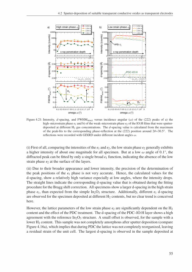
4.2 Sputter-deposition of suitable transparent conductive oxides as transparent electrodes
1
1 0
1 0 0
1 0 0 0
1 0 0 0 0
1
1 0
1 0 0
1 0 0 0
1 0 0 0 0
2 . 9 2
2 . 9 3
2 . 9 4
2 . 9 2
2 . 9 3
2 . 9 4
0 . 1 0 . 3 0 . 5 0 . 7 0 . 9 1 . 1 1 . 3 1 . 5 1 . 7 1 . 9 30 . 0
0 . 2
0 . 4
0 . 6
0 . 8
0 . 1 0 . 3 0 . 5 0 . 7 0 . 9 1 . 1 1 . 3 1 . 5 1 . 7 1 . 9 30 . 0
0 . 2
0 . 4
0 . 6
0 . 8
L o w s t r a i n p h a s e 2 0 . 0 % H 2 1 . 0 % H 2 2 . 0 % H 2 2 . 8 % H 2
Inten
sity (c
ounts
)
H 2
b )
x - r a y p e n e t r a t i o n d e p t h
0 . 0 % H 2 1 . 0 % H 2 2 . 0 % H 2 2 . 8 % H 2
Inten
sity (c
ounts
)
H i g h s t r a i n p h a s e 1
o n l y 1
x - r a y p e n e t r a t i o n d e p t h
P D C - I O : H
a )
H 2
I n 2 O 3 ( 2 2 2 )I n 2 O 3 ( 2 2 2 )
d-spa
cing (
Å)
d-spa
cing (
Å)
FWHM
struc
t (°)
o m e g a ( ° )
FWHM
struc
t (°)
o m e g a ( ° )
Figure 4.21: Intensity, d-spacing, and FWHMstruct versus incidence angular (ω) of the (222) peaks of a) thehigh–microstrain phase ε1 and b) of the weak–microstrain phase ε2 of the IO:H films that were sputter-deposited at different H2 gas concentrations. The d-spacing value is calculated from the maximumof the peak-fits to the corresponding phase-reflection at the (222) position around 2θ=30.5°. Thereflections were recorded with GIXRD under different incident angles ω.
(i) First of all, comparing the intensities of the ε1 and ε2, the low strain phase ε2 generally exhibitsa higher intensity of about one magnitude for all specimen. But at a low ω angle of 0.1°, thediffracted peak can be fitted by only a single broad ε1 function, indicating the absence of the lowstrain phase ε2 at the surface of the layers.
(ii) Due to their broader appearance and lower intensity, the precision of the determination ofthe peak positions of the ε1 phase is not very accurate. Hence, the calculated values for thed-spacing, show a relatively high variance especially at low angles, where the intensity drops.The straight lines indicate the corresponding d-spacing value that is obtained during the fittingprocedure for the Bragg shift correction. All specimens show a larger d-spacing in the high strainphase ε1, than expected from the simple In2O3 structure. Additionally, different ε1 d-spacingare observed for the specimen deposited at different H2 contents, but no clear trend is conceivedhere.
However, the lattice parameters of the low strain phase ε2 are significantly dependent on the H2content and the effect of the PDC treatment. The d-spacing of the PDC–IO:H layer shows a highagreement with the reference In2O3 structure. A small offset is observed, for the sample with alower H2 content. This sample was not completely amorphous after sputter deposition (compareFigure 4.16a), which implies that during PDC the lattice was not completely reorganized, leavinga residual strain of the unit cell. The largest d-spacing is observed in the sample deposited at
55

4 Development of perovskite solar cells for tandem application
1.0 % H2. Probably the strain of the unit cell originates from the interstitial hydrogen doping.It seems, that the annealing step did not release the stress of the lattice. A large d-spacing isalso obtained from the sample that was deposited without H2 addition. Here, the strain mightbe introduced by oxygen doping.
(iii) Evaluation of the FWHMstruct indicates that the H2 content has also a high influence on thebroadening of both peak functions ε1 and ε2. A reduced broadening speaks for a low microstrainε , which would indicate a low density of defects. As expected, the high strain phase ε1 exhibitslarge FWHM, especially in the samples with low H2 content. In ε2, these samples show also ahigher strain, than the PDC–IO:H layers.
In order to quantify the amount of strain broadening, that each phase contributes to the diffractionpattern at a certain incident angle, Figure 4.22 shows the relative peak intensities of ε1 and ε2normalized to 100 % versus ω. The colour coding describes the amount of microstrain ε that iscalculated from the FWHMstruct for each phase.
100
2810 11 10 10 10 10 11 12 12
7290 89 90 90 90 90 89 88 88
100
16 10 11 10 11 13 10 13 16 11
84 90 89 90 89 87 90 87 84 89
100
28 24 25 2336 30 25 26 37 26
72 76 75 7764 70 75 74 63 74
100 100
7 13 11 14 9 9 13 15 10
93 87 89 86 91 91 87 85 90
0.1 0.3 0.5 0.7 0.9 1.1 1.3 1.5 1.7 1.9 3
incident angle w (°)
0.1 0.3 0.5 0.7 0.9 1.1 1.3 1.5 1.7 1.9 3
norm
alis
ed p
eak in
tensity (
%)
incident angle w (°)
0.0
0.1
0.2
0.3
0.4
0.5
0.6
0.7
0.8
0.9
1.0
1.1
1.2
1.3
1.4
microstrain
e (%)
0% H2
1.0% H2
2.0% H2
2.8% H2
ε2
ε1
ε2
ε1
ε2
ε1
ε2
ε1
Figure 4.22: Bar diagrams showing the ratio of the maximum intensity (denoted in %) of the ε1 and ε2 (222) peaksversus ω for IO:H samples, which were deposited at different H2 gas concentrations. The colour codeindicates the corresponding microstrain (ε) that is obtained from the FWHMstruct of each peak.
At a small ω of 0.1°, only the high strain phase ε1 is observed in all specimens. At this angleclose to ωc, the penetration depth of the incident beam is only several nanometres, indicatinga ε1 layer with a high density of defects at the surface of the samples. The strain in this layeris higher than 1 %. Noticeable, the PDC–IO:H sample (2.8 % H2) exhibits a thicker ε1 surfacelayer up to 0.3°, but here the strain of ε1 is generally lower (0.7 % to 0.8 %) as indicated by thecolor code.
56

4.2 Sputter-deposition of suitable transparent conductive oxides as transparent electrodes
At higher ω, the contribution of ε2 dominates, which implies that ε2 has a dominant presencein the bulk. A higher strain between 0.3 % to 0.4 % is determined for the bulk phase ε2 ofsamples with low hydrogen content, compared to the samples deposited at 2.0 % and 2.8 % H2that exhibit a low ε2 strain of 0.1 % to 0.2 %. The contribution of the ε1 phase is measurable atall angles, most likely originating from the ε1 surface layer, but an additional presence of ε1 inthe bulk may not be excluded.
In case of the 2.0 % H2 sample, the ε1 to ε2 signal ratio is higher as compared to the othersamples, which is due to the lower maximum intensity of the (222) peaks in the samples. Hence,the ε2 signal is reduced. In contrast, the preferential lattice orientation in the samples depositedat a low H2 content leads to a higher ε2 peak intensity (compare Figure 4.21b).
Comparing the ε values obtained from theWilliamson-Hall evaluation in Table 4.1 with the onesfor ε2 from the GIXRD investigation, a goodmatch is observed, indicating a rather homogeneousmicrostrain level throughout the layer thickness. The GIXRD results prove, that a thin layer atthe surface of all samples exhibit an increased microstrain, which implies a higher defect density.
For the application of the IO:H layers as front electrodes in solar cells, two main conclusionsmay be conceived.
(i) PDC–IO:H deposited at 2.8 % H2 shows the best crystallographic properties in terms of alow microstrain, thus a low defect density, and a undistorted unit cell, thus a low doping level.The low defect density contributes to a high charge carrier mobility (µ), because defects actas scattering centres. The low doping level results in a low Ne, which reduces the free carrierabsorption at in the NIR range. Both properties are only achievable, when the IO:H layer isdeposited amorphously prior to a PDC. Some residual microstrain in the layer indicates thatthere is still room for improvements, to decrease the defect density even further and achieve evenhigher µ values.
(ii) The thin top layer that exhibits a higher amount of microstrain, might not contribute much tothe macroscopic optical and electrical properties of the film, but it could cause deviations of theinterface properties, when it is in contact with the ETL in the solar cell. Without knowledge ofthe nature of the strain causing defects, it is difficult to foretell, if they have a significant effecton the charge extraction or injection in the final device.
4.2.3 Comparison between optimized IZO and IO:H layers and commercialavailable TCO substrates
This section compares the optimized IO:H and IZO materials to the commercially availableTCOs such as FTO and ITO that are primarily used in PSC. Additionally, ZAO is includedin the comparison, because it represents the standard TCO in CIGS solar cell technology, [67]which is also utilized in the CIGS cells that are introduced later on in this study.
Figure 4.23a shows representative absorptance spectra of the set of TCO layers. Their individualthickness is denoted in the diagram legend. As expected, the in-house prepared TCOs exhibit asmaller A than the commercial TCO layers.
57

4 Development of perovskite solar cells for tandem application
Big differences are also observed in the position of the optical band gap (Eg). For the comparedmaterials, FTO and ITO show the highest optical band gapswith approximately (3.95 ± 0.05) eV.a-IO:H exhibits an optical band gap of (3.85 ± 0.03) eV, increasing up to (3.90 ± 0.03) eV afterthe annealing step (PDC–IO:H). For these high band gap values of FTO, ITO, as-deposited andannealed IO:H a larger uncertainty is assumed because the absorption edge of the glass substratemay affects the TCO absorption edge. Nevertheless, the calculated band gap values agree withinthe accuracy with the stated values in literature [115, 118, 119]. IZO and ZAO exhibit smallerband gaps of (3.79 ± 0.02) eV and (3.63 ± 0.02) eV and hence can be determined with a higheraccuracy. These values are comparable as well with values given in the literature [63, 83].Optical band gap calculations are performed as described in Section 3.2.1.
For illustrating the impact of the different A responses, Figure 4.23b depicts the cumulative JAbsof the layers in the range from 300 nm to 1300 nm. With respect to application in tandem cells,it is meaningful to divide the solar spectrum in the UV/Vis range and the NIR range. The insetsof the diagram show the JAbs of the layers in these two ranges. Over the full spectrum range,FTO exhibits the largest JAbs of over 7 mA cm−2, partly reasoned by the large layer thickness of550 nm. ITO has also a high loss of about 5 mA cm−2, followed by ZAO. IZO and a-IO:H showlow losses of about 2 mA cm−2 and PDC–IO:H stays below 1 mA cm−2. In the UV/Vis range,the IZO and ZAO layers have quite high losses of up to 1.6 mA cm−2 due to their comparablynarrow band gap. The NIR regime sees the highest losses in ITO and FTO.
In order to compare the optical properties of the layers to the conductive ones, 4.23c shows theAwt versus Rsq for the set of TCO layers and for the different spectrum ranges as indicated. Here,two a-IO:H and PDC–IO:H layers are added, which have an increased film thickness of 230 nm.With the Rsq reduced by 5Ω, they are suitable candidates for a more efficient front electrodecompared to the thinner layers. The increased film thickness also leads to an increased Awt.However, even with the larger thickness PDC–IO:H outperforms all other TCOs with a ultra lowAwt of about 2 % over the full spectrum at an Rsq of 15Ω. ITO and FTO exhibit both a betterconductivity with Rsq values down to 7Ω, but they have a significant Awt deficit, especially inthe NIR range.
a) b) c)
400 600 800 1000 12000
10
20
30
40
50
60
70
FTO 550 nm
ITO 120 nm
IZO 180 nm
ZAO 335 nm
a-IO:H 170 nm
PDC-IO:H 170 nm
A (
%)
Wavelength (nm)
0
1
2
3
4
5
6
7
400 600 800 1000 12000
1
2
3
4
FTO IZO
ITO a-IO:H
ZAO PDC-IOH
JA
bs (
mA
cm
-2)
Ne,d
NIR
Wavelength (nm)
UV/Vis
5 10 15 20 25 30 35 40 45
0
2
4
6
8
10
12
14
16
18
20
ZAO
330 nm
IZO
180 nm
PDC-IO:H
170 nm
a-IO:H
230 nm
ITO
135 nm
Awt integration range
300-800 nm (UV/Vis)
300-1300 nm (total)
800-1300 nm (NIR)
Aw
t (%
)
Rsq (W")
FTO
550 nm
Figure 4.23: a) Absorptance spectra of different TCO materials. IZO, a-IO:H and PDC–IO:H layers are comparedwith standard process ZAO, ITO and FTO. b) JAbs curves for the respective TCOs over the totalspectral range from 300 nm to 1300 nm and in the UV/Vis and NIR range (insets). c)Awt versus Rsqplot for the same layers in the respective spectral ranges. Additionally, the data for IO:H layers withan increased thickness of 230 nm is shown as indicated.
58

4.3 Semitransparent perovskite solar cells
The significant differences between the materials are attributed to their electrical properties.Hall measurements of both, in-house and commercial materials, revealed strong variation incarrier concentration and mobility as depicted in Figure 4.24. The benchmark for the opticalproperties is set by PDC–IO:H with its low Ne of 1.83 × 1020 cm−3. Due to the high µ, it reachesalso good conductive properties with a ρ of 380 µΩ cm, making it the best candidate for the frontelectrode. ZAO has also a low Ne, hence a low Awt in NIR, but suffers from a low µ. In orderto reach an acceptable Rsq, the layer thickness has to be chosen quite large. IZO shows the thirdlowest Ne of 3.88 × 1020 cm−3, which makes it a good NIR transmitter. In combination witha fairly low ρ, IZO resembles the most promising material for application as a rear electrode.FTO has a increased Ne and a mediocre µ and the film thickness of the commercial productis large in order to achieve a good Rsq. In total, this combination results in the worst opticalproperties. a-IO:H shows similar values, so even with a reduced film thickness, the Awt staysbehind the one of IZO. ITO sets the benchmark for the lowest ρ of 162 µΩ cm, but the goodconductive properties can not compensate for the high Awt introduced by the exceptionally highNe of 11.4 × 1020 cm−3.
380
1410
372 355 292 162
1.83.1 3.9
5.2 6.0
11.4
90
14
4334 35 34
0
400
800
1200
1600
r (
mW
cm
)
0
3
6
9
12
Ne(1
02
0cm
-3)
PDC-IO
:HZAO
IZO
FTO
a-IO
:H ITO
0
30
60
90
m (
cm
2 V
-1s
-1)
Figure 4.24: Hall measurements of different TCOmaterials. Depicted are ρ, Ne, and µ for in-house and commercial(FTO, ITO) TCOs.
Concluding, annealed PDC–IO:H is particularly suitable as a front electrode in PSCs withsuperstrate configuration, because of the high band gap, the outstanding NIR absorption andlow sheet resistance. Importantly, the annealing step can be carried out after deposition on theglass superstrate. It outperforms the commercial TCOs mainly in terms of NIR transmittance.For the rear electrode, both IZO and a-IO:H seem to be suitable candidates, with IZO having anadvantage over a-IO:H as it has a better NIR transmission and good conductivity.
4.3 Semitransparent perovskite solar cells
The transition from opaque to semitransparent PSCs requires the exchange of the metal rearelectrode with a transparent alternative. In the last chapter, IZO and a-IO:H have been identifiedas suitable candidates, offering a high transmittance and a good conductivity. The task of thefirst Section 4.3.1 is the deposition of the new electrodes on to the PSC without damaging thesensitive underlying layers.
59
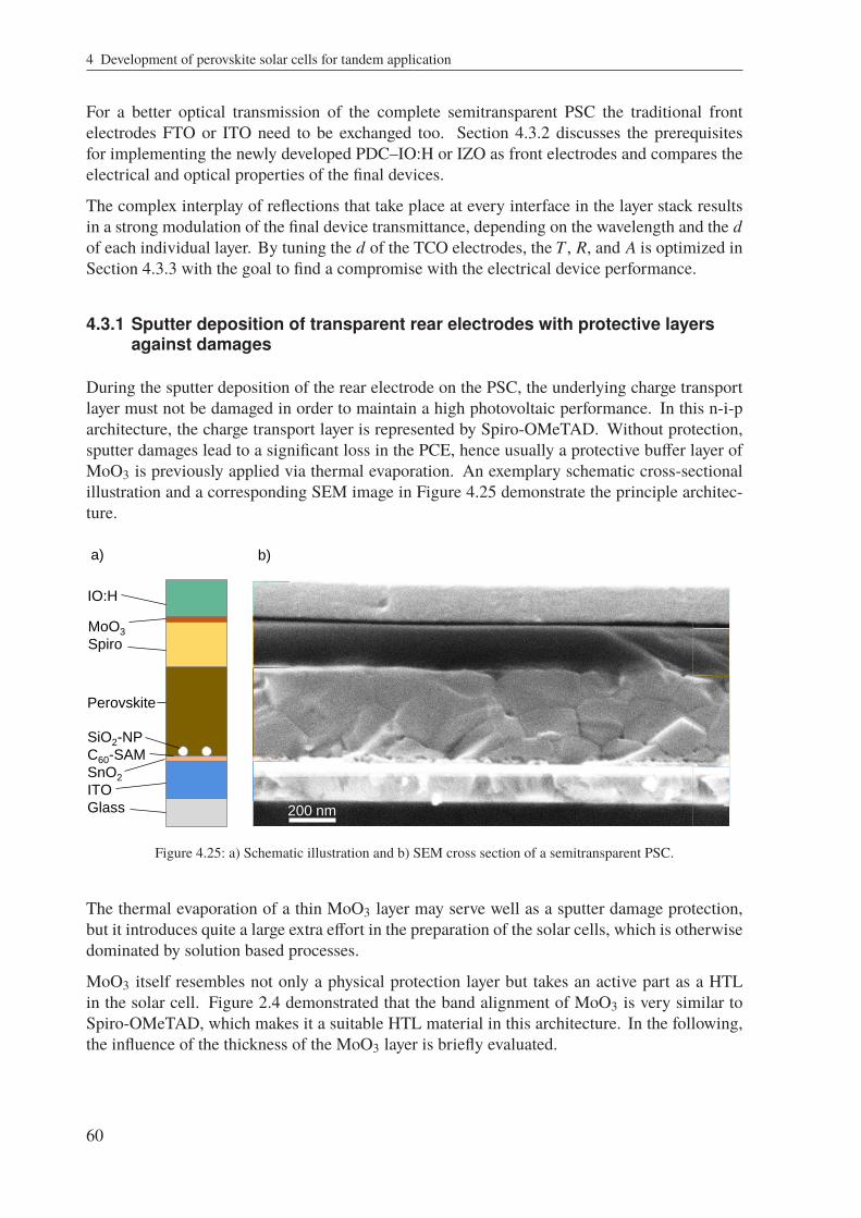
4 Development of perovskite solar cells for tandem application
For a better optical transmission of the complete semitransparent PSC the traditional frontelectrodes FTO or ITO need to be exchanged too. Section 4.3.2 discusses the prerequisitesfor implementing the newly developed PDC–IO:H or IZO as front electrodes and compares theelectrical and optical properties of the final devices.
The complex interplay of reflections that take place at every interface in the layer stack resultsin a strong modulation of the final device transmittance, depending on the wavelength and the dof each individual layer. By tuning the d of the TCO electrodes, the T , R, and A is optimized inSection 4.3.3 with the goal to find a compromise with the electrical device performance.
4.3.1 Sputter deposition of transparent rear electrodes with protective layersagainst damages
During the sputter deposition of the rear electrode on the PSC, the underlying charge transportlayer must not be damaged in order to maintain a high photovoltaic performance. In this n-i-parchitecture, the charge transport layer is represented by Spiro-OMeTAD. Without protection,sputter damages lead to a significant loss in the PCE, hence usually a protective buffer layer ofMoO3 is previously applied via thermal evaporation. An exemplary schematic cross-sectionalillustration and a corresponding SEM image in Figure 4.25 demonstrate the principle architec-ture.
MoO3
SiO2-NP
C60-SAM
SnO2
ITO
Glass
a) b)
Perovskite
MoO3
Spiro
IO:H
200 nm
Figure 4.25: a) Schematic illustration and b) SEM cross section of a semitransparent PSC.
The thermal evaporation of a thin MoO3 layer may serve well as a sputter damage protection,but it introduces quite a large extra effort in the preparation of the solar cells, which is otherwisedominated by solution based processes.
MoO3 itself resembles not only a physical protection layer but takes an active part as a HTLin the solar cell. Figure 2.4 demonstrated that the band alignment of MoO3 is very similar toSpiro-OMeTAD, which makes it a suitable HTL material in this architecture. In the following,the influence of the thickness of the MoO3 layer is briefly evaluated.
60

4.3 Semitransparent perovskite solar cells
Furthermore, two alternative protection layer free concepts will be investigated. Reports onthe possibility to heal sputter damages by annealing steps [144] raise the question whetherthe sputter damages to Spiro-OMeTAD could be cured similarly, when no protection layer wasused. Another approach includes the avoidance or reduction of the initial damaging using mildersputter conditions.
Recovery from sputter damage through annealing
In order to investigate if the sputter damage to the Spiro-OMeTAD could be cured with anannealing step, a series of different annealing temperatures and times was applied to PSCs. Theresults of the according JV scans are reported in Figure 4.26a and b. The first graph showsthe JV responses of a single PSC, that was annealed at 50 C, 60 C, 65 C and 70 C for 300 sbefore each measurement in consecutive order. It proves, that up to 65 C there is indeed acuring effect observable, resulting in a beneficial shift of the curves towards higher voltages.However, at 70 C the JV response indicates a thermal damage by JSC loss and a reduced parallelresistance (Rp).
The second graph in Figure 4.26b demonstrates with a second PSC, that increasing the annealingto 30 min at the temperature of 65 C leads to a further curing, as the s-shape of the JV responseis significantly reduced. Unfortunately, further heating for another 30 min, in total 60 min, hasagain a disadvantageous effect on the performance.
0.0 0.4 0.8 1.2
-20
-15
-10
-5
0
Annealing
for 300 s at
50 °C
60 °C
65 °C
70 °C
J (
mA
cm
-2)
V (V)0.0 0.4 0.8 1.2
-20
-15
-10
-5
0
Annealing
at 65 °C for
0 min
30 min
60 min
J (
mA
cm
-2)
V (V)
a) b)
Figure 4.26: Impact of the a) annealing temperature and b) annealing time on the JV-responses of PSCs em-ploying no protective layer in the architecture ITO/SnO2-NP/C60-SAM/SiO2-NP/CsFAMAPIBr/Spiro-OMeTAD/IZO.
The results indicate, that the sputter damage can partly be cured by annealing. Presumably, thedamaged parts of the HTL get cured by mechanisms related to interdiffusion and reorganizationof the molecules at elevated temperatures. However, since the Spiro-OMeTAD itself is vulner-able to elevated temperatures, the curing effect is soon overcome by a degradation effect. Inconclusion, annealing is not applicable to fully recover the sputter damages dealt to a PSC ofthis architecture.
61
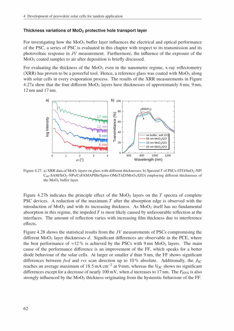
4 Development of perovskite solar cells for tandem application
Thickness variations of MoO3 protective hole transport layer
For investigating how the MoO3 buffer layer influences the electrical and optical performanceof the PSC, a series of PSC is evaluated in this chapter with respect to its transmission and itsphotovoltaic response in JV measurement. Furthermore, the influence of the exposure of theMoO3 coated samples to air after deposition is briefly discussed.
For evaluating the thickness of the MoO3 even in the nanometre regime, x-ray reflectometry(XRR) has proven to be a powerful tool. Hence, a reference glass was coated with MoO3 alongwith solar cells in every evaporation process. The results of the XRR measurements in Figure4.27a show that the four different MoO3 layers have thicknesses of approximately 6 nm, 9 nm,12 nm and 17 nm.
600 800 1000 12000
20
40
60
80
100
Tra
nsm
itta
nce (
%)
Wavelength (nm)
no buffer, soft IZO
05 nm MoO3/IZO
10 nm MoO3/IZO
20 nm MoO3/IZO
d(MoO3)
0 1 2 3 4
6 nm
9 nm
12 nm
log I
nte
nsity
w (°)
17 nm
a) b)
Figure 4.27: a) XRR data of MoO3 layers on glass with different thicknesses; b) SpectralT of PSCs (ITO/SnO2-NP/C60-SAM/SiO2-NPs/CsFAMAPIBr/Spiro-OMeTAD/MoO3/IZO) employing different thicknesses ofthe MoO3 buffer layer.
Figure 4.27b indicates the principle effect of the MoO3 layers on the T spectra of completePSC devices. A reduction of the maximum T after the absorption edge is observed with theintroduction of MoO3 and with its increasing thickness. As MoO3 itself has no fundamentalabsorption in this regime, the impeded T is most likely caused by unfavourable reflection at theinterfaces. The amount of reflection varies with increasing film thickness due to interferenceeffects.
Figure 4.28 shows the statistical results from the JV measurements of PSCs compromising thedifferent MoO3 layer thicknesses d. Significant differences are observable in the PCE, wherethe best performance of ≈12 % is achieved by the PSCs with 9 nm MoO3 layers. The maincause of the performance difference is an improvement of the FF, which speaks for a betterdiode behaviour of the solar cells. At larger or smaller d than 9 nm, the FF shows significantdifferences between fwd and rvs scan direction up to 10 % absolute. Additionally, the JSCreaches an average maximum of 18.5 mA cm−2 at 9 mm, whereas the VOC shows no significantdifferences except for a decrease of nearly 100 mV, when d increases to 17 nm. The FHYS is alsostrongly influenced by the MoO3 thickness originating from the hysteretic behaviour of the FF.
62
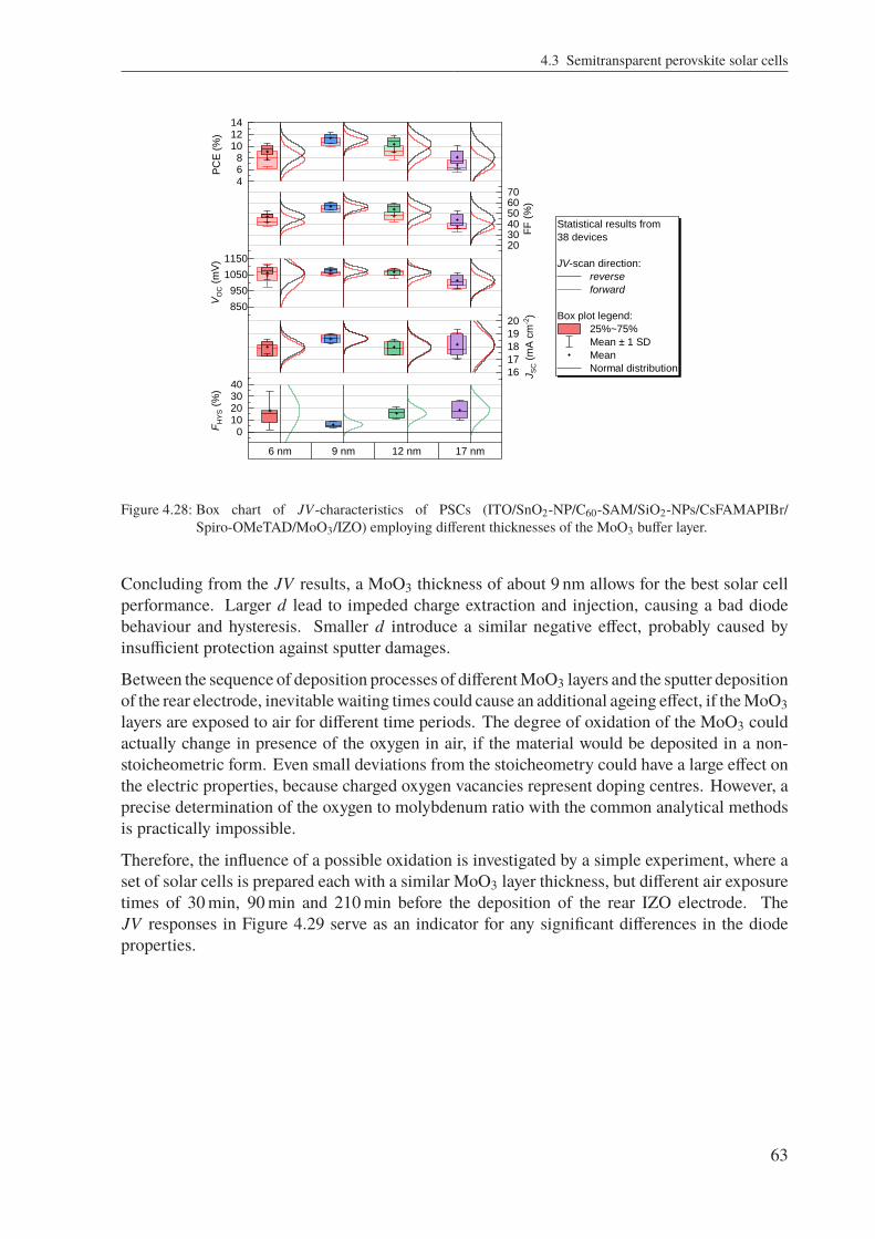
4.3 Semitransparent perovskite solar cells
468
101214
PC
E (
%)
Statistical results from
38 devices
JV-scan direction:
reverse
forward
Box plot legend:
25%~75%
Mean ± 1 SD
Mean
Normal distribution
203040506070
FF
(%
)
850
950
1050
1150
VO
C (
mV
)
16
17
18
19
20
JS
C (
mA
cm
-2)
6 nm 9 nm 12 nm 17 nm
010203040
FH
YS (
%)
Figure 4.28: Box chart of JV-characteristics of PSCs (ITO/SnO2-NP/C60-SAM/SiO2-NPs/CsFAMAPIBr/Spiro-OMeTAD/MoO3/IZO) employing different thicknesses of the MoO3 buffer layer.
Concluding from the JV results, a MoO3 thickness of about 9 nm allows for the best solar cellperformance. Larger d lead to impeded charge extraction and injection, causing a bad diodebehaviour and hysteresis. Smaller d introduce a similar negative effect, probably caused byinsufficient protection against sputter damages.
Between the sequence of deposition processes of differentMoO3 layers and the sputter depositionof the rear electrode, inevitablewaiting times could cause an additional ageing effect, if theMoO3layers are exposed to air for different time periods. The degree of oxidation of the MoO3 couldactually change in presence of the oxygen in air, if the material would be deposited in a non-stoicheometric form. Even small deviations from the stoicheometry could have a large effect onthe electric properties, because charged oxygen vacancies represent doping centres. However, aprecise determination of the oxygen to molybdenum ratio with the common analytical methodsis practically impossible.
Therefore, the influence of a possible oxidation is investigated by a simple experiment, where aset of solar cells is prepared each with a similar MoO3 layer thickness, but different air exposuretimes of 30 min, 90 min and 210 min before the deposition of the rear IZO electrode. TheJV responses in Figure 4.29 serve as an indicator for any significant differences in the diodeproperties.
63
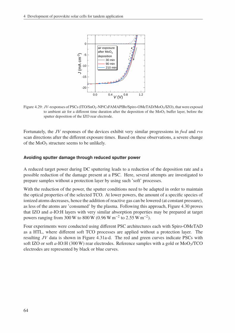
4 Development of perovskite solar cells for tandem application
0.0 0.4 0.8 1.2
-20
-15
-10
-5
0
air exposure
after MoO3
deposition
30 min
90 min
210 min
J (
mA
cm
-2)
V (V)
Figure 4.29: JV-responses of PSCs (ITO/SnO2-NP/CsFAMAPIBr/Spiro-OMeTAD/MoO3/IZO), that were exposedto ambient air for a different time duration after the deposition of the MoO3 buffer layer, before thesputter deposition of the IZO rear electrode.
Fortunately, the JV responses of the devices exhibit very similar progressions in fwd and rvsscan directions after the different exposure times. Based on these observations, a severe changeof the MoO3 structure seems to be unlikely.
Avoiding sputter damage through reduced sputter power
A reduced target power during DC sputtering leads to a reduction of the deposition rate and apossible reduction of the damage present at a PSC. Here, several attempts are investigated toprepare samples without a protection layer by using such ’soft’ processes.
With the reduction of the power, the sputter conditions need to be adapted in order to maintainthe optical properties of the selected TCO. At lower powers, the amount of a specific species ofionized atoms decreases, hence the addition of reactive gas can be lowered (at constant pressure),as less of the atoms are ’consumed’ by the plasma. Following this approach, Figure 4.30 provesthat IZO and a-IO:H layers with very similar absorption properties may be prepared at targetpowers ranging from 300 W to 800 W (0.96 W m−2 to 2.55 W m−2).
Four experiments were conducted using different PSC architectures each with Spiro-OMeTADas a HTL, where different soft TCO processes are applied without a protection layer. Theresulting JV data is shown in Figure 4.31a-d. The red and green curves indicate PSCs withsoft IZO or soft a-IO:H (300 W) rear electrodes. Reference samples with a gold or MoO3/TCOelectrodes are represented by black or blue curves.
64

4.3 Semitransparent perovskite solar cells
400 600 800 1000 12000
10
20
30
40
50
Absorp
tance (
%)
Wavelength (nm)
IZO, 800W, 1.2% O2
IZO, 600W, 1.0% O2
IZO, 300W, 0.6% O2
a-IO:H, 800W, 2.8% O2, 2.8% H2
a-IO:H, 300W, 1.8% O2, 2.0% H2
Figure 4.30: Spectral absorptance of different IZO and IO:H layers from sputter processes with varied power.
0.0 0.4 0.8 1.2
-20
-15
-10
-5
0
5
10
15
20
25
30
35
40
45
50
ITO/c-SnO2/C60-SAM/SiO2-NP/
CsFAMAPBrI/spiro-MeOTAD
600W
Gold
softIZO
J (
mA
cm
-2)
V (V)0.0 0.4 0.8 1.2
-20
-15
-10
-5
0
5
10
15
20
25
30
35
40
45
50
ITO/ALD-SnO2/C60-SAM/SiO2-NP/
WBG-Perovskite/spiro-MeOTAD
300W
MoO3/IZO
MoO3/IO:H
softIZO
softIO:H
J (
mA
cm
-2)
V (V)
0.0 0.4 0.8 1.2
-20
-15
-10
-5
0
5
10
15
20
25
30
35
40
45
50
ITO/c-SnO2/
CsFAMAPbBrI/spiro-MeOTAD
300W
Gold
MoO3/IO:H
softIO:H
J (
mA
cm
-2)
V (V)0.0 0.4 0.8 1.2
-20
-15
-10
-5
0
5
10
15
20
25
30
35
40
45
50
ITO/SnO2-NP/C60-SAM/SiO2-NP/
CsFAMAPBrI/spiro-MeOTAD
300W
MoO3/IZO
softIZO
J (
mA
cm
-2)
V (V)
a) b)
c) d)
Figure 4.31: Current voltage characteristics of devices with and without MoO3 buffer layer, applying differentsputter processes with reduced power.
Despite the reduced power, a strong s-shape is present in the JV responses of the cells with softTCO rear electrodes, which indicates a corrupted interface and the evidence of sputter damages.The simple reduction of the target power is not effectively avoiding the damaging of the HTL.One reason could be that the reduction of the power is reducing mainly the current flow through
65

4 Development of perovskite solar cells for tandem application
the plasma, but the target voltage for establishing the plasma stays relatively constant. As a result,the number of accelerated ions may be reduced that hit the sample surface per time interval, buttheir kinetic energy is still high enough to deal damage. Therefore, the sputter conditions shouldbe varied so that the kinetic energy of the bombardment is reduced.
4.3.2 Implementation of IZO and PDC-IO:H as front electrodes with ultra-low NIRabsorption
IZO and IO:H demonstrated their superior optical performance in comparison to ITO and FTOalready in Chapter 4.2.3 and they were successfully implemented as a transparent rear electrodein perovskite solar cells. These results promise a further improvement of the optical propertiesof the PSCs, if also the front electrode is replaced by IZO or IO:H. Therefore, this sectionevaluates the optical and photovoltaic properties of PSCs with FTO, ITO, PDC–IO:H and IZOas front electrodes.
Figure 4.32 depicts the statistical results of the photovoltaic performance of opaque andsemitransparent PSCs employing the different front electrodes. The PSC architecture isfront electrode/SnO2-NP/C60-SAM/SiO2-NP/CsFAMAPIBr/Spiro-OMeTAD/rear electrode. Asthe normal distribution curves of the PCE values of the opaque cells in Figure 4.32a indicate,a narrow distribution is only reached with ITO with an average PCE over 15 %. PSCs withother TCOs struggle with a lower average PCE, despite the capability of FTO and PDC–IO:H toreach high maximum PCE values close to 17 %. The main cause of the scattered distribution aredeviations in the FF. Since ITO is the electrode material predominantly used for developmentof the architecture, the well optimized processes could explain the small statistical deviations.In case of FTO, the comparably rougher surface might be one reason for the reproducibilityproblems and also for the larger FHYS. The PSCs with in-house developed TCOs front electrodesmight be impeded by particle contaminations of the glass superstrate, which are believed tocause local shunts.
However, the results of the JSC indicate a significant improvement with PDC–IO:H. An averagegain of ≈1 mA cm−2 is observed compared to the other TCOs, which is probably due to theexceptional transmission of the PDC–IO:H.
Similar results are observed with semitransparent PSCs in Figure 4.32b, where the gold rearcontact is replaced by a-IO:H. Here the JSC gain of PDC–IO:H is not as large as in the opaquesetup, due to the missing back reflection from the gold rear electrode.
66
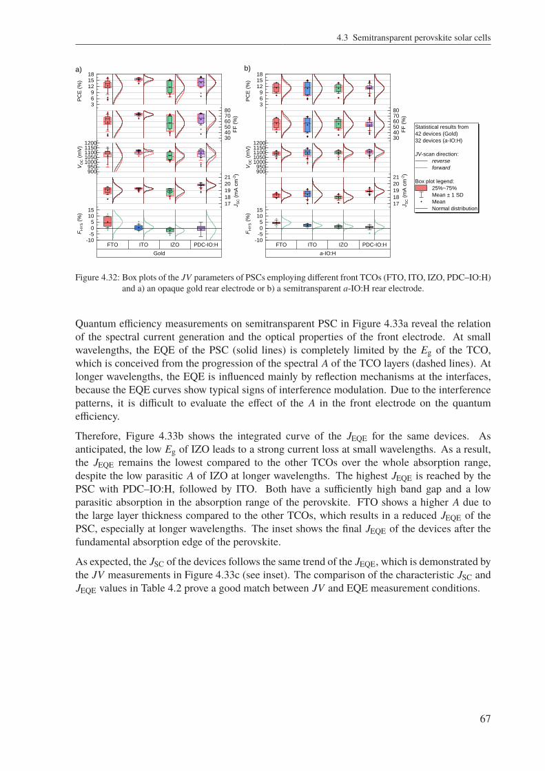
4.3 Semitransparent perovskite solar cells
369
121518
PC
E (
%)
Statistical results from
42 devices (Gold)
32 devices (a-IO:H)
JV-scan direction:
reverse
forward
Box plot legend:
25%~75%
Mean ± 1 SD
Mean
Normal distribution
304050607080
FF
(%
)
900950
10001050110011501200
VO
C (
mV
)
17
18
19
20
21
JS
C (
mA
cm
-2)
FTO ITO IZO PDC-IO:H
a-IO:H
-10-505
1015
FH
YS (
%)
369
121518
PC
E (
%)
304050607080
FF
(%
)
900950
10001050110011501200
VO
C (
mV
)
17
18
19
20
21
JS
C (
mA
cm
-2)
FTO ITO IZO PDC-IO:H
Gold
-10-505
1015
FH
YS (
%)
a) b)
Figure 4.32: Box plots of the JV parameters of PSCs employing different front TCOs (FTO, ITO, IZO, PDC–IO:H)and a) an opaque gold rear electrode or b) a semitransparent a-IO:H rear electrode.
Quantum efficiency measurements on semitransparent PSC in Figure 4.33a reveal the relationof the spectral current generation and the optical properties of the front electrode. At smallwavelengths, the EQE of the PSC (solid lines) is completely limited by the Eg of the TCO,which is conceived from the progression of the spectral A of the TCO layers (dashed lines). Atlonger wavelengths, the EQE is influenced mainly by reflection mechanisms at the interfaces,because the EQE curves show typical signs of interference modulation. Due to the interferencepatterns, it is difficult to evaluate the effect of the A in the front electrode on the quantumefficiency.
Therefore, Figure 4.33b shows the integrated curve of the JEQE for the same devices. Asanticipated, the low Eg of IZO leads to a strong current loss at small wavelengths. As a result,the JEQE remains the lowest compared to the other TCOs over the whole absorption range,despite the low parasitic A of IZO at longer wavelengths. The highest JEQE is reached by thePSC with PDC–IO:H, followed by ITO. Both have a sufficiently high band gap and a lowparasitic absorption in the absorption range of the perovskite. FTO shows a higher A due tothe large layer thickness compared to the other TCOs, which results in a reduced JEQE of thePSC, especially at longer wavelengths. The inset shows the final JEQE of the devices after thefundamental absorption edge of the perovskite.
As expected, the JSC of the devices follows the same trend of the JEQE, which is demonstrated bythe JV measurements in Figure 4.33c (see inset). The comparison of the characteristic JSC andJEQE values in Table 4.2 prove a good match between JV and EQE measurement conditions.
67

4 Development of perovskite solar cells for tandem application
a) b) c)
400 600 8000
20
40
60
80
100
PSC EQE
TCO 1-A
EQ
E,
1-A
(%
)
Wavelength (nm)
Front TCO
FTO, 550 nm
ITO, 120 nm
IZO, 170 nm
PDC-IO:H, 185 nm
TCO Eg
400 600 8000
5
10
15
20
750 800
18.0
18.5
19.0
19.5
JE
QE (
mA
cm
-2)
Wavelength (nm)
FTO
ITO
IZO
PDC-IO:H
TCO Eg
0.0 0.2 0.4 0.6 0.8 1.0 1.2
-20
-15
-10
-5
0
5
0.0 0.4 0.8-20.0
-19.5
-19.0
-18.5
-18.0
FTO
ITO
IZO
PDC-IO:H
J (
mA
cm
-2)
V (V)
Figure 4.33: a) EQE and A responses of semitransparent PSCs with different front TCOs (FTO, ITO, IZO,PDC–IO:H); b) JEQE curves of the same samples, the inset shows the integrated JEQE at the ab-sorption edge; c) JV curves of the same PSCs, the inset allows a more detailed investigation of theJSC.
Regarding the optical performance of the PSCs for future tandem application, the transmittance(T), reflectance (R) and absorptance (A) of the devices are evaluated in Figure 4.34a and b. Asintended, the use of PDC–IO:H and IZO as front electrodes leads to a significant increase ofT and a reduction of A. Notably, the device with ITO exhibits a strong R between 100 nm to1200 nm due to the high Ne of ITO compared to the other TCO materials. This leads to a strongreduction of T , while the highest A is observed in the PSC with FTO.
In order to quantify the parasitic absorption of the PSC in the spectral range after the absorptionedge of the perovskite, Figure 4.34c shows the integrated JAbs from 800 nm to 1300 nm. BothPSCs with PDC–IO:H and IZO exhibit significantly reduced JAbs, which corresponds to areduction of about 50 % compared to the commercial TCOs. The exact values are listed in Table4.2.
600 800 1000 12000
20
40
60
80
100 FTO ITO
IZO PDC-IO:H
T,
R (
%)
Wavelength (nm)
400 600 800 1000 12000
20
40
60
80
100 FTO
ITO
IZO
PDC-IO:H
A (
%)
Wavelength (nm)
a) b) c)
800 900 1000 1100 1200 13000
1
2
3
4
5
6
7 FTO
ITO
IZO
PDC-IO:H
JA
bs (
mA
cm
-2)
Wavelength (nm)
Figure 4.34: a) Transmittance (solid), reflectance (dashed) and b) absorptance spectra for perovskite solar cells withdifferent front TCO contacts of commercial (ITO, FTO) and in-house materials (IZO, PDC–IO:H).Amorphous IO:H was used as TCO back contact. c) JAbs of the same samples in for wavelengthsafter the absorption edge of the perovskite, indicating the equivalent current losses due to free carrierabsorption in the front TCOs.
68

4.3 Semitransparent perovskite solar cells
The results promise a great impact on the performance of the bottom cell in a tandem setup,when the front TCO of the semitransparent top cell is replaced by PDC–IO:H or IZO. Theirreduced parasitic absorption will allow for a increased quantum yield in the bottom cell. But thecomparably low band gap of IZO is unfavourable for the tandem performance, since it cuts offpart of the blue light, hence reducing the current generation in the top cell. PDC–IO:H offersfull potential for efficient top and bottom cells. A detailed evaluation of tandem architecturescomprising different TCO combination follows in Section 5.3.
4.3.3 The optical influence of TCO layer thickness
In order to determine the influence of the thickness of the front- and rear electrodes on theoptical properties of semitransparent PSCs, this section evaluates the T , R and A of deviceswith a variety of IO:H contact layers. The PSCs of the architecture PDC–IO:H/SnO2/C60-SAM/SiO2-NP/CsFAMAPIBr/Spiro-OMeTAD/MoO3/a-IO:H use PDC–IO:H as front electrodes withdfront of 100 nm, 160 nm, 220 nm and 300 nm and a-IO:H as rear electrodes with drear of 90 nm,160 nm and 240 nm.
Figure 4.35 depict the spectral R, T and A of the PSCs with all combinations of dfront and drearin form of colour maps.
The R data is shown for the range from 300 nm to 1300 nm, covering the absorption andtransmission range of the PSC. In the absorption range up to ≈800 nm, R is dominated byreflection at the front electrode, which leads to interference patterns strongly related to dfront.A dominant green colour indicates a small amount of reflection in this range regardless of thethickness of the front electrode. In the transmission range after 800 nm, the reflection at therear electrode interface with air causes a great effect on the spectral R. Depending on drear, Ris modulated strongly by interference effects. This leads to R values of over 25 %, especiallywhen the rear electrode layer is thin.
In correspondence to the reflection, the spectral T is also affected strongly by drear. Generally,following 1 = T + R + A, T is low, when R is high, so a thick rear electrode seems to befavourable. But increasing drear leads to higher absorption, which counteracts the effect.
The increase of A with d is observed in Figure 4.35c. Especially drear has a strong impact onthe absorptance ratio. This is due to the higher Ne in the a-IO:H compared to the PDC–IO:H ofthe front electrode. A higher Ne leads to increased free carrier absorption and reflection.
69
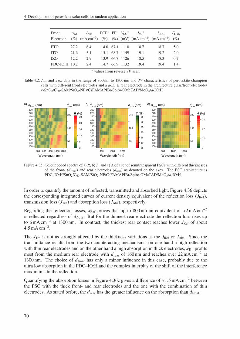
4 Development of perovskite solar cells for tandem application
Front Awt JAbs PCE∗ FF∗ VOC∗ JSC∗ JEQE FHYS
Electrode (%) (mA cm−2) (%) (%) (mV) (mA cm−2) (mA cm−2) (%)
FTO 27.2 6.4 14.0 67.1 1110 18.7 18.7 5.0ITO 21.6 5.1 15.1 68.7 1149 19.1 19.2 2.0IZO 12.2 2.9 13.9 66.7 1126 18.5 18.3 0.7PDC-IO:H 10.2 2.4 14.7 66.9 1132 19.4 19.4 1.4
∗ values from reverse JV scan
Table 4.2: Awt and JAbs data in the range of 800 nm to 1300 nm and JV characteristics of perovskite championcells with different front electrodes and a a-IO:H rear electrode in the architecture glass/front electrode/c-SnO2/C60-SAM/SiO2-NPs/CsFAMAPIBr/Spiro-OMeTAD/MoO3/a-IO:H.
400 600 800 1000 1200
100
160
220
300
100
160
220
300
100
160
220
300
Wavelength (nm)
dfront (nm)
3
8
13
18
23
28
R (%)
90
160
240
drear (nm)
800 1000 1200
100
160
220
300
100
160
220
300
100
160
220
300
Wavelength (nm)
dfront (nm)
55
60
65
70
75
80
85
T (%)
90
160
240
drear (nm)
800 1000 1200
100
160
220
300
100
160
220
300
100
160
220
300
Wavelength (nm)
dfront (nm)
7
12
17
22
A (%)
90
160
240
drear (nm)a) b) c)
Figure 4.35: Colour coded spectra of a) R, b) T , and c) A of a set of semitransparent PSCs with different thicknessesof the front- (dfront) and rear electrodes (drear) as denoted on the axes. The PSC architecture isPDC–IO:H/SnO2/C60-SAM/SiO2-NP/CsFAMAPIBr/Spiro-OMeTAD/MoO3/a-IO:H.
In order to quantify the amount of reflected, transmitted and absorbed light, Figure 4.36 depictsthe corresponding integrated curves of current density equivalent of the reflection loss (JRef),transmission loss (JTrn) and absorption loss (JAbs), respectively.
Regarding the reflection losses, JRef proves that up to 800 nm an equivalent of ≈2 mA cm−2
is reflected regardless of dfront. But for the thinnest rear electrode the reflection loss rises upto 6 mA cm−2 at 1300 nm. In contrast, the thickest rear contact reaches lower JRef of about4.5 mA cm−2.
The JTrn is not as strongly affected by the thickness variations as the JRef or JAbs. Since thetransmittance results from the two counteracting mechanisms, on one hand a high reflectionwith thin rear electrodes and on the other hand a high absorption in thick electrodes, JTrn profitsmost from the medium rear electrode with drear of 160 nm and reaches over 22 mA cm−2 at1300 nm. The choice of dfront has only a minor influence in this case, probably due to theultra low absorption in the PDC–IO:H and the complex interplay of the shift of the interferencemaximums in the reflection.
Quantifying the absorption losses in Figure 4.36c gives a difference of ≈1.5 mA cm−2 betweenthe PSC with the thick front- and rear electrodes and the one with the combination of thinelectrodes. As stated before, the drear has the greater influence on the absorption than dfront.
70

4.3 Semitransparent perovskite solar cells
400 600 800 1000 12000
1
2
3
4
5
6 Perovskite
Absorption
drear
dfront (nm)
100
160
220
300
drear (nm)
90
160
240
JR
ef (m
A c
m-2
)
Wavelength (nm)
Reflection at
rear electrode
a) b) c)
800 900 1000 1100 1200 13004
6
8
10
12
14
16
18
20
22
dfront (nm)
100
160
220
300
drear (nm)
90
160
240
JT
rn (
mA
cm
-2)
Wavelength (nm)
800 900 1000 1100 1200 13000
1
2
3
4
dfront
JA
bs (
mA
cm
-2)
Wavelength (nm)
dfront (nm)
100
160
220
300
drear (nm)
90
160
240
drear
Figure 4.36: a) JRef, b) JTrn, and c) JAbs curves of semitransparent PSCs with different thicknesses of the front-(dfront) and rear electrodes (drear) as denoted by the colours and symbols. The PSC architecture isPDC–IO:H/SnO2/C60-SAM/SiO2-NP/CsFAMAPIBr/Spiro-OMeTAD/MoO3/a-IO:H.
Following the previous optical results it would make sense to reduce the thickness of both TCOlayers of front and rear electrode as much as possible in order to minimize A. However, thesheet resistance increases strongly with decreasing thickness, as shown in Section 4.2.1, finallylimiting the photovoltaic performance of the PSC. Furthermore, the R modulates strongly withthe thickness of the rear electrode. Following the fresnel equation 2.9, the amount of reflectionat the rear interface can be reduced by a anti reflection coating (ARC) coating with suitablerefractive indices. Tuning the thickness of all layers, including the ARC layer, could furtherreduce the internal reflection losses by minimizing the interference effects.
In order to investigate the influence of the sheet resistance of the rear electrode on the performanceof the PSC, Figure 4.37a and b show the JV responses of PSCs with different rear electrodesgold, IO:H and IZO. Additionally, the sheet resistances of the corresponding TCO layers onglass are denoted in the graph. As expected, the series resistance for thinner TCO layers withhigher Rsq increases, which is noticeable from the decreased slope of the JV response at VOC.To quantify the series resistance, the slope dV/dJ(V) at VOC is used to extract a resistance valuenormalized to the cell area. This resistance can be used as a measure for series resistance (Rs),but does not correspond exactly to it [120].
Figure 4.37c shows a box plot of the resulting resistance in comparison to the Rsq of thecorresponding rear electrode. The application of thin TCO layers with a Rsq of 40Ω results inmuch higher resistance values of over 15Ω cm2 compared to a gold rear electrode with 7Ω cm2.As the thickness increases, the resistance decreases significantly. For the 220 nm layer with aRsq of 15Ω the resistances drop to 10Ω cm2 to 12Ω cm2. This corresponds to a reduction of30 % with an approximate doubling of the layer thickness.
71

4 Development of perovskite solar cells for tandem application
-0.2 0.0 0.2 0.4 0.6 0.8 1.0 1.2 1.4
-20
-10
0
10
20
30
40
50
60
J (
mA
cm
-2)
V (V)
100nm IO:H, 40W"
170nm IO:H, 18W"
220nm IO:H, 15W"
64nm Gold, 0.3W"
-0.2 0.0 0.2 0.4 0.6 0.8 1.0 1.2 1.4
-20
-10
0
10
20
30
40
50
60
J (
mA
cm
-2)
V (V)
64nm Gold, 0.3W"
100nm IZO, 40W"
160nm IZO, 22W"
220nm IZO, 15W"
a) b)
c) d)
Gold a-IO:H IZO a-IO:H IZO a-IO:H IZO
0.3 15 18 22 40
8
10
12
14
16
Rsq (W")
PC
E (
%)
50
55
60
65
70
75
FF
(%
)
Gold a-IO:H IZO a-IO:H IZO a-IO:H IZO
0.3 15 18 22 40
5
10
15
20
25
Rsq (W")
dV
/dJ(J
=0)
(W c
m2)
Figure 4.37: Representative JV scans for perovskite solar cells with a) IO:H and b) IZO back contacts of differentthickness. Solar cells with gold contact were measured as reference samples. c) Box plot of the slopedV/dJ at V = 0 as quantification of the Rs and d) effect on FF of the JV curves.
The lower series resistance directly influences the FF and thus the PCE as depicted in Figure4.37d. The FF of the semitransparent cells increase in average from ≈50 % to over 60 % whendrear increases from 100 nm to 220 nm and the Rsq drops from 40Ω to 15Ω, respectively. Interms of PCE this corresponds to a gain of 2 % absolute.
Nevertheless, the PCE of the semitransparent PSCs are significantly lower than the value of thegold reference with a fill factor of 67.5 % in average. This is partly due to the superior Rsq of0.3Ω (gold on glass) which is 40 times lower than of the 220 nm TCO layer.
In conclusion, the layer thickness of the transparent electrodes is a decisive factor for the opticaland photovolatic performance of the PSC. Especially the rear electrode has a major influenceon the absorption and the reflectance in the NIR regime. Here, a rather thin layer would bebeneficial, but this limits the PCE of the PSC by a high series resistance.
Generally, the series resistance is also interlinked with the geometry of the solar cell. In thissetup, the active area has a size of 7 × 3.25mm2. If the cell dimensions would be much smallerand the contacts close to the active area, then the Rs would be also less important for the PCE.This is a fundamental aspect that has to be acknowledged, when it comes to optimizing theoptical and electrical properties of the PSC for tandem applications.
72

4.3 Semitransparent perovskite solar cells
For implementing the PSC in a 4T-tandem cell with CIGS, the PSC active area needs to be evenincreased, which would cause additional losses due to a higher Rs. One possible solution toreduce the Rs of the semitransparent PSCs is the application of a metal grid to the rear electrode,which is part of the discussion about tandem solar cells in the next Chapter 5.
73


5 Four-terminal perovskite–CIGS tandem cells
In this chapter the semitransparent perovskite cells are integrated into four-terminal tandem cellswith CIGS as a bottom cell. Figure 5.1 gives a schematic overview of the development stepsthat are discussed in the following.
Top Cell
Bottom Cell
CIGS
4T Tandem
5.2 Bottom Cell
5.1 Setup and Design
Superstrate
5.3 Devices
FiltersTransparent electrode
Perovskite
HTLIO:H
4.3 Semitransparent Cell area
Top cell grid
Band Gap
Electrodes
IZO
Multi Cation
4. Perovskite Top Cell
ETL
5. Tandem Cell
5.4 Optimization
Transparent Electrode Loss analysisOptical coupling
ABX3 Perovskite
Wide Band Gap
IO:HIZO
ITO
Band gaps Performance
Simulation
Simulation
Figure 5.1: Strategy for developing the 4-terminal tandem cell using a n-i-p–perovskite top cell and CIGS bottomcell with indicated chapter numeration.
The first Section 5.1 covers the general design aspects of the tandem cell, considering the cell sizematching and grid integration. Secondly, in order to estimate the CIGS bottom cell photovoltaicperformance, modelling approach is discussed in Section 5.2. Section 5.3 evaluates the actualperformance of tandem devices with different architectures, comprising perovskite and CIGSsolar cells with different band gaps and electrodes. For a deeper understanding of the optical andelectrical mechanisms that limit the tandem power conversion efficiency, current loss analysesare performed in Section 5.4.1. From the findings of the loss analysis, further development stepssuch as the use of optical coupling materials and anti reflective coatings are tested. Additionally,also the impact of wide band gap PSCs with ultra-high transmission is simulated in order to findthe maximum achievable bottom cell efficiency.
75

5 Four-terminal perovskite–CIGS tandem cells
5.1 Design and performance aspects of four-terminal tandemarchitectures
For the development of four-terminal tandem architectures, two different approaches are chosenin this work. The first approach is often used for estimating the tandem device performance bycombining an optical filter that shall represent the PSC with the CIGS bottom cell as shown inFigure 5.2a. This approach gives the opportunity to fabricate smaller sized PSCs along with alarger filter of a nominally identical layer stack. Both the PSC and the filtered CIGS solar cellare measured separately and the single values are used for estimating a theoretical value for thePCE of a possible tandem device.
Since it is more convenient and reproducible, to achieve high performance PSCs on a small activearea, this approach is commonly used to assess different possible tandem setups. Furthermore,as the filter does not need electrical connections, the mechanical integration is simplified. Thisallows for e.g., the use of optical coupling materials to fill the air gap between the CIGS cell andthe filter, such as immersion oil.
A more sophisticated approach is to stack a semitransparent PSC and a CIGS cell of the samesize as depicted in Figure 5.2b. This represents a fully functional 4T-tandem cell. Electricaland optical measurements are performed simultaneously with this architecture and the resultsare representative for a real 4T-tandem device as all relevant aspects are already included inthe design. These aspects include variations of the transmittance of the perovskite, cell sizedependent losses originating from the lateral conductivity of the electrodes or losses introducedby the shadow casting of the grids of the subcells.
+
+
−
−
4T-Tandem
Cell
b)
+
−
+
−
4T-Tandem
Estimation
Filter
a)
Figure 5.2: Schematic illustrations of different approaches to tandem solar cell development: a) For estimating theperformance of the bottom cell in a tandem setup, an optical filter is used that shall represent the topcell. The top cell itself has a non-matching geometry and is measured separately. b) The top and thebottom cell with matched cell sizes are mechanically stacked on top of each other. Optical and electricalmeasurements are performed simultaneously.
In the following, themismatch of the transmission between different filters and the correspondingPSCs is discussed briefly in Section 5.1.1. The impact of the increase of the active area of thePSC is discussed in Section 5.1.2 along with the integration of a metal grid, for the use in4T-tandem cells.
76

5.1 Design and performance aspects of four-terminal tandem architectures
5.1.1 Optical mismatch between perovskite solar cells and representative filterdevices
Quite commonly, tandem performances are estimated by using a representative filter in place ofthe actual PSC as a top cell, with the belief that the actual transmittance is represented preciselyenough by the filter. But due to many layer preparation steps and variations in the processes,most likely the filter exhibits a certain deviance from the sister PSC, even if prepared in the samerun with the same process parameters. This chapter investigates briefly the possible opticaldifferences between filters and cells.
Figure 5.3a shows two typical transmittance (T) curves of PSCs with different electrodes (solidlines) and alongside the corresponding T of a similarly prepared set of filter stacks (dashed).Obviously, the coarse trend of the PSC T is followed by the filters, but the exact positions ofthe interference maxima and minimums are shifted quite significantly. Even small deviationsin the film thicknesses or roughness can cause a significant shift of the maxima, because of thewavelength sensitive internal reflection mechanisms at the interfaces between the layers. Thishas been already demonstrated by variations of the electrode thicknesses in Section 4.3.3.
The question remains, if this resembles a significant impact on the average transmittance or moreprecisely on the transmitted photon flux. Additionally to the T curves, Figure 5.3a shows thecurrent density equivalent of the photon flux (qNph) of the AM1.5. As the photon flux declineswith longer wavelengths and exhibits some gaps, the deviations of the T should be weightedaccording to qNph.
600 800 1000 1200
T× qN
ph (
mA
cm
-2 n
m-1
)
wavelength (nm)
0.00
0.01
0.02
0.03
0.04
0.05
0.06
0.07
0.01
0.03
0.05
0.07
0.09
PSC (ITO-IO:H)
Filter (ITO-IO:H)
PSC (IOH-IO:H)
Filter (IOH-IO:H)
600 800 1000 12000.0
0.2
0.4
0.6
0.8
1.0
T,
qN
ph (
mA
cm
-2 n
m-1
)
wavelength (nm)
a) b)
600 800 1000 1200
∫ T
× qN
ph d
l (
mA
cm
-2)
wavelength l (nm)
0
2
4
6
8
10
12
14
16
18
20
22
24
PSC (ITO-IO:H)
Filter (ITO-IO:H)
PSC (IOH-IO:H)
Filter (IOH-IO:H)
c)
Figure 5.3: a) Transmittance T of PSCs and representative filter samples of the same architecture with differ-ent front TCOs (TCO/SnO2-NP/C60-SAM/SiO2-NPs/CsFAMAPIBr/conductive fluorene/MoO3/IO:H);The gray coloured data shows the photon flux of the AM1.5G spectrum in equivalents of current densityqNph. b) Transmittance of the same samples multiplied by the photon flux T · qNph. c) Integral curvesof b.
Bymultiplication of T ·qNph a direct weighting is achieved as shown in the graph of Figure 5.3b.Usually, these graphs are not convenient to compare, but the integral curve from Figure 5.3c canbe used to estimate the maximum number of photons that are transmitted through the PSC up toa certain wavelength limit. The integrated value expresses the current density equivalent of thetransmission (JTrn) (see equation 2.12), which represents the maximum current density givendirectly in the units mA cm−2 that a perfect solar cell could gain from the transmitted photonflux in the dedicated wavelength range.
77

5 Four-terminal perovskite–CIGS tandem cells
The integrated curves demonstrate that the JTrn of the filters does not largely deviate from theJTrn of the cells. Actually, depending on the upper integration limit, the JTrn values might matchprecisely.
In order to set the JTrn in proportion to the incident photon flux, a weighted average transmittance(Twt) value is introduced in analogy to T , following equation 2.16.
Using these two values JTrn and Twt for evaluation the T spectra of filters and cells, gives adirectly understandable and comparable quantification of the principle mismatch.
Table 5.1 shows the results for a set of PSCs and corresponding filters with a variety of differentTCO combinations. The integration limits are chosen from 300 nm to 1200 nm. Remarkably,the filters all exhibit a higher Twt than the PSC samples. The relative mismatch is below 1 % forthe samples with ITO or FTO front electrode, but for IZO and IO:H it reaches up to 3.6 %. Interms of JTrn, the absolute mismatch of the filter would account for an additional transmissionof over 0.5 mA cm−2.
Setup PSC Filter Abs. Mismatch Rel. Mismatch
Front Rear JTrn Twt JTrn Twt ∆JTrn ∆Twt ∆
TCO TCO (mA cm−2) (%) (mA cm−2) (%) (mA cm−2) (%) (%)
ITO IZO 16.1 40.2 16.1 40.4 +0.07 +0.18 +0.45ITO IO:H 15.9 39.8 16.0 40.0 +0.05 +0.12 +0.31
FTO IZO 16.9 42.2 17.0 42.5 +0.12 +0.30 +0.70FTO IO:H 16.8 42.1 16.9 42.2 +0.03 +0.08 +0.18
IZO IZO 18.6 46.5 19.1 47.9 +0.54 +1.35 +2.91IZO IO:H 18.5 46.4 19.2 48.0 +0.66 +1.66 +3.58
IO:H IZO 19.0 47.7 19.6 49.0 +0.54 +1.35 +2.84IO:H IO:H 19.0 47.6 19.5 48.7 +0.45 +1.13 +2.37
Table 5.1: The current density equivalent of the transmission (JTrn) and the weighted average transmittance (Twt)of PSCs and representative filter samples of the same architecture with different front- and rearTCOs (front TCO/SnO2-NP/C60-SAM/SiO2-NPs/CsFAMAPIBr/conductive fluorene/MoO3/rear TCO);The values are calculated from the spectral transmittance of the samples using the equations 2.12 and2.16 within the integration limits of 500 nm to 1200 nm. The relative mismatch ∆ is calculated by(JTrn(Filter)/JTrn(PSC) − 1).
Since the highest mismatch is observed with IZO and IO:H front electrodes, which are preparedin-house, this suggests that there are greater deviations in the layer thickness homogeneitycompared to the commercial TCOs such as FTO and ITO. Moreover, the rear electrode issputter deposited on the full area of the filter samples, while framed metal aperture masks areused for the PSCs in order to define the active area. This may have a significant influence onthe temperature of the samples and the plasma properties during sputtering, which could resultin different optical properties of the rear TCOs. The general trend of the increased transmissionof the filters may be explained by this.
78
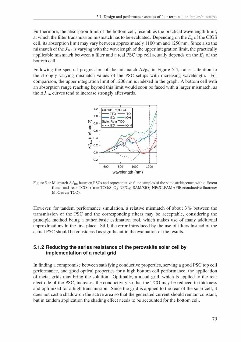
5.1 Design and performance aspects of four-terminal tandem architectures
Furthermore, the absorption limit of the bottom cell, resembles the practical wavelength limit,at which the filter transmission mismatch has to be evaluated. Depending on the Eg of the CIGScell, its absorption limit may vary between approximately 1100 nm and 1250 nm. Since also themismatch of the JTrn is varying with the wavelength of the upper integration limit, the practicallyapplicable mismatch between a filter and a real PSC top cell actually depends on the Eg of thebottom cell.
Following the spectral progression of the mismatch ∆JTrn in Figure 5.4, raises attention tothe strongly varying mismatch values of the PSC setups with increasing wavelength. Forcomparison, the upper integration limit of 1200 nm is indexed in the graph. A bottom cell withan absorption range reaching beyond this limit would soon be faced with a larger mismatch, asthe ∆JTrn curves tend to increase strongly afterwards.
600 800 1000 1200
-0.2
0.0
0.2
0.4
0.6
0.8
1.0
1.2
DJ
Trn
(m
A c
m-2
)
wavelength (nm)
Colour: Front TCO
FTO ITO
IZO IOH
Style: Rear TCO
IZO IO:H
Figure 5.4: Mismatch ∆JTrn between PSCs and representative filter samples of the same architecture with differentfront- and rear TCOs (front TCO/SnO2-NP/C60-SAM/SiO2-NPs/CsFAMAPIBr/conductive fluorene/MoO3/rear TCO).
However, for tandem performance simulation, a relative mismatch of about 3 % between thetransmission of the PSC and the corresponding filters may be acceptable, considering theprinciple method being a rather basic estimation tool, which makes use of many additionalapproximations in the first place. Still, the error introduced by the use of filters instead of theactual PSC should be considered as significant in the evaluation of the results.
5.1.2 Reducing the series resistance of the perovskite solar cell byimplementation of a metal grid
In finding a compromise between satisfying conductive properties, serving a good PSC top cellperformance, and good optical properties for a high bottom cell performance, the applicationof metal grids may bring the solution. Optimally, a metal grid, which is applied to the rearelectrode of the PSC, increases the conductivity so that the TCO may be reduced in thicknessand optimized for a high transmission. Since the grid is applied to the rear of the solar cell, itdoes not cast a shadow on the active area so that the generated current should remain constant,but in tandem application the shading effect needs to be accounted for the bottom cell.
79
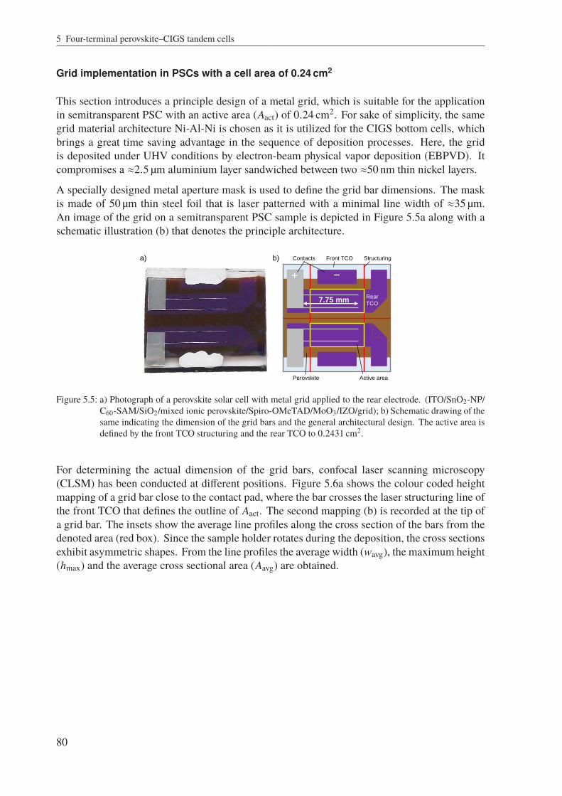
5 Four-terminal perovskite–CIGS tandem cells
Grid implementation in PSCs with a cell area of 0.24 cm2
This section introduces a principle design of a metal grid, which is suitable for the applicationin semitransparent PSC with an active area (Aact) of 0.24 cm2. For sake of simplicity, the samegrid material architecture Ni-Al-Ni is chosen as it is utilized for the CIGS bottom cells, whichbrings a great time saving advantage in the sequence of deposition processes. Here, the gridis deposited under UHV conditions by electron-beam physical vapor deposition (EBPVD). Itcompromises a ≈2.5 µm aluminium layer sandwiched between two ≈50 nm thin nickel layers.
A specially designed metal aperture mask is used to define the grid bar dimensions. The maskis made of 50 µm thin steel foil that is laser patterned with a minimal line width of ≈35 µm.An image of the grid on a semitransparent PSC sample is depicted in Figure 5.5a along with aschematic illustration (b) that denotes the principle architecture.
7.75 mm
+ −
a) b)
Rear
TCO
Front TCO StructuringContacts
Active areaPerovskite
Figure 5.5: a) Photograph of a perovskite solar cell with metal grid applied to the rear electrode. (ITO/SnO2-NP/C60-SAM/SiO2/mixed ionic perovskite/Spiro-OMeTAD/MoO3/IZO/grid); b) Schematic drawing of thesame indicating the dimension of the grid bars and the general architectural design. The active area isdefined by the front TCO structuring and the rear TCO to 0.2431 cm2.
For determining the actual dimension of the grid bars, confocal laser scanning microscopy(CLSM) has been conducted at different positions. Figure 5.6a shows the colour coded heightmapping of a grid bar close to the contact pad, where the bar crosses the laser structuring line ofthe front TCO that defines the outline of Aact. The second mapping (b) is recorded at the tip ofa grid bar. The insets show the average line profiles along the cross section of the bars from thedenoted area (red box). Since the sample holder rotates during the deposition, the cross sectionsexhibit asymmetric shapes. From the line profiles the average width (wavg), the maximum height(hmax) and the average cross sectional area (Aavg) are obtained.
80

5.1 Design and performance aspects of four-terminal tandem architectures
0 20 40 60 80 100 120 140
0
20
40
60
80
100
x (µm)
y (
µm
)
0
20
40
60
80
100
0 1 2
wavg
y (
µm
)
h (µm)
hmax = 1.7 µm
wavg = 48 µm
Aavg = 50 µm2
0 20 40 60 80 100 120 140
0
20
40
60
80
100
x (µm)
y (
µm
)
0.0
0.4
0.8
1.2
1.6
2.0
h (µm)
0
20
40
60
80
100
0 1 2
hmax = 2.0 µm
wavg = 34 µm
Aavg = 40 µm2
y (
µm
)
h (µm)
wavg
a) b)no IT
O
ITO
Figure 5.6: Coloured topographical scans from CLSM of solar cells (ITO/SnO2-NP/C60-SAM/SiO2/mixed ionic perovskite/Spiro-OMeTAD/MoO3/IZO/grid) at different positions of the grid bars: a) nearthe contact pad at the laser line defining the active area, and b) at the tip. The insets show averaged linescan profiles along the marked areas.
Due to the aperture mask design, the grid bar is wider near the pad and narrower at the tip.From tip to pad, wavg changes approximately linearly from 34 µm to 48 µm. Additionally, hmaxdecreases from 2.0 µm to 1.7 µm, respectively. As a result the Aavg increases from 40 µm2 to50 µm2, which is reasonable because the current density increases in direction of the pad anda larger cross section aids the conductivity. Because the single grid bars do not show largedeviations in their aspect ratios, mean values of Aavg ≈ 45 µm2 and wavg ≈ 41 µm can beestimated for further calculations.
In order to evaluate the effect of the grid on the performance of a PSC, Figure 5.7a compares theJV responses of PSCs with grid (blue curve) and without grid (red) to a reference solar cell witha gold rear electrode (black). The inset shows the PCEs during dynamic MPP tracking. Fromthe slope of the JV curves at forward bias, a significant improvement of the Rs is anticipatedwhen the grid is applied. Compared to the sample without grid, this results in a better FF andthe diode behaviour converges the one with gold electrode. This leads to an efficiency leap sothat both PSCs with IZO/grid and gold electrode achieve PCEs well over 16 % in MPP tracking,while the sample with simple IZO electrode reaches only 14 %.
81
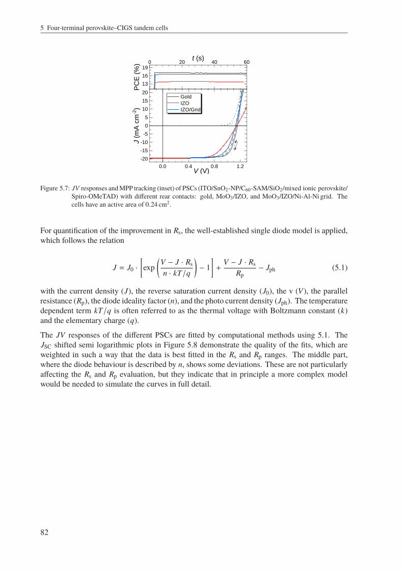
5 Four-terminal perovskite–CIGS tandem cells
0.0 0.4 0.8 1.2
-20
-15
-10
-5
0
5
10
15
20 Gold
IZO
IZO/Grid
J (
mA
cm
-2)
V (V)
0 20 40 60
13
16
19
t (s)
PC
E (
%)
Figure 5.7: JV responses andMPP tracking (inset) of PSCs (ITO/SnO2-NP/C60-SAM/SiO2/mixed ionic perovskite/Spiro-OMeTAD) with different rear contacts: gold, MoO3/IZO, and MoO3/IZO/Ni-Al-Ni grid. Thecells have an active area of 0.24 cm2.
For quantification of the improvement in Rs, the well-established single diode model is applied,which follows the relation
J = J0 ·
[exp
(V − J · Rsn · kT/q
)− 1
]+
V − J · RsRp
− Jph (5.1)
with the current density (J), the reverse saturation current density (J0), the v (V), the parallelresistance (Rp), the diode ideality factor (n), and the photo current density (Jph). The temperaturedependent term kT/q is often referred to as the thermal voltage with Boltzmann constant (k)and the elementary charge (q).
The JV responses of the different PSCs are fitted by computational methods using 5.1. TheJSC shifted semi logarithmic plots in Figure 5.8 demonstrate the quality of the fits, which areweighted in such a way that the data is best fitted in the Rs and Rp ranges. The middle part,where the diode behaviour is described by n, shows some deviations. These are not particularlyaffecting the Rs and Rp evaluation, but they indicate that in principle a more complex modelwould be needed to simulate the curves in full detail.
82
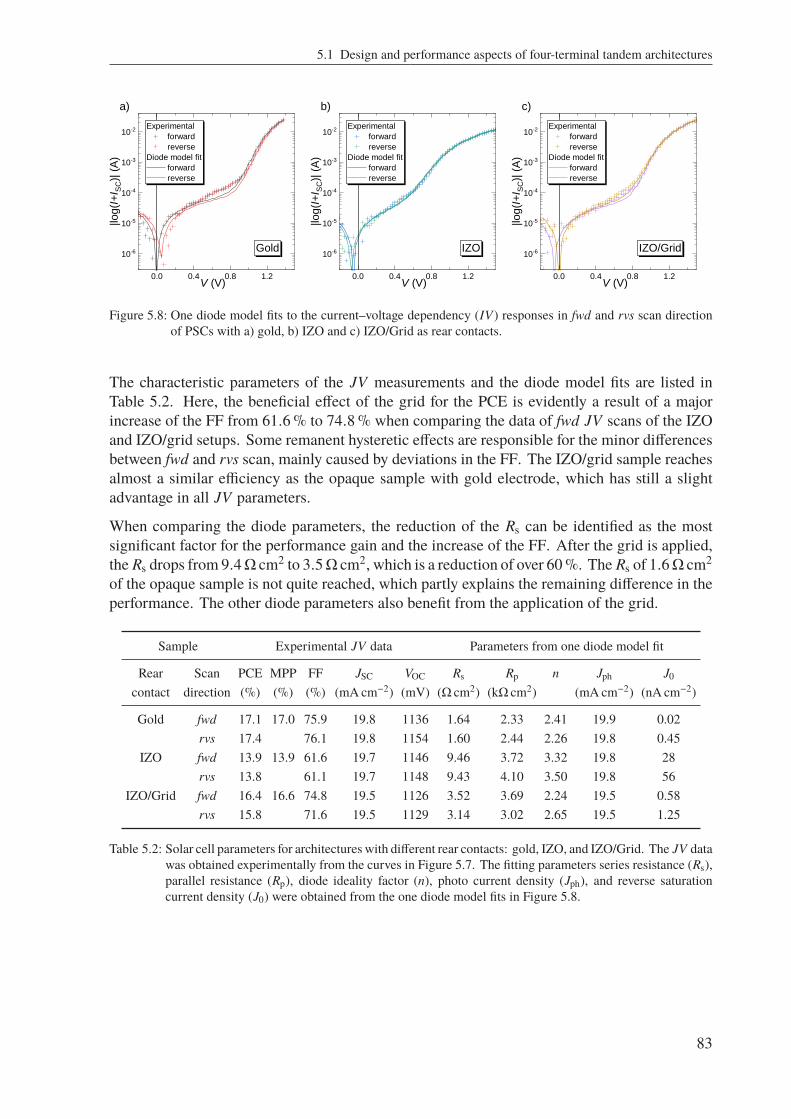
5.1 Design and performance aspects of four-terminal tandem architectures
a) b) c)
0.0 0.4 0.8 1.2
10-6
10-5
10-4
10-3
10-2
Gold
Experimental
forward
reverse
Diode model fit
forward
reverse
|log(I
+I S
C)|
(A
)
V (V)0.0 0.4 0.8 1.2
10-6
10-5
10-4
10-3
10-2Experimental
forward
reverse
Diode model fit
forward
reverse
|log(I
+I S
C)|
(A
)
V (V)
IZO
0.0 0.4 0.8 1.2
10-6
10-5
10-4
10-3
10-2
IZO/Grid
Experimental
forward
reverse
Diode model fit
forward
reverse
|log(I
+I S
C)|
(A
)
V (V)
Figure 5.8: One diode model fits to the current–voltage dependency (IV) responses in fwd and rvs scan directionof PSCs with a) gold, b) IZO and c) IZO/Grid as rear contacts.
The characteristic parameters of the JV measurements and the diode model fits are listed inTable 5.2. Here, the beneficial effect of the grid for the PCE is evidently a result of a majorincrease of the FF from 61.6 % to 74.8 % when comparing the data of fwd JV scans of the IZOand IZO/grid setups. Some remanent hysteretic effects are responsible for the minor differencesbetween fwd and rvs scan, mainly caused by deviations in the FF. The IZO/grid sample reachesalmost a similar efficiency as the opaque sample with gold electrode, which has still a slightadvantage in all JV parameters.
When comparing the diode parameters, the reduction of the Rs can be identified as the mostsignificant factor for the performance gain and the increase of the FF. After the grid is applied,the Rs drops from 9.4Ω cm2 to 3.5Ω cm2, which is a reduction of over 60 %. The Rs of 1.6Ω cm2
of the opaque sample is not quite reached, which partly explains the remaining difference in theperformance. The other diode parameters also benefit from the application of the grid.
Sample Experimental JV data Parameters from one diode model fit
Rear Scan PCE MPP FF JSC VOC Rs Rp n Jph J0
contact direction (%) (%) (%) (mA cm−2) (mV) (Ω cm2) (kΩ cm2) (mA cm−2) (nA cm−2)
Gold fwd 17.1 17.0 75.9 19.8 1136 1.64 2.33 2.41 19.9 0.02rvs 17.4 76.1 19.8 1154 1.60 2.44 2.26 19.8 0.45
IZO fwd 13.9 13.9 61.6 19.7 1146 9.46 3.72 3.32 19.8 28rvs 13.8 61.1 19.7 1148 9.43 4.10 3.50 19.8 56
IZO/Grid fwd 16.4 16.6 74.8 19.5 1126 3.52 3.69 2.24 19.5 0.58rvs 15.8 71.6 19.5 1129 3.14 3.02 2.65 19.5 1.25
Table 5.2: Solar cell parameters for architectures with different rear contacts: gold, IZO, and IZO/Grid. The JV datawas obtained experimentally from the curves in Figure 5.7. The fitting parameters series resistance (Rs),parallel resistance (Rp), diode ideality factor (n), photo current density (Jph), and reverse saturationcurrent density (J0) were obtained from the one diode model fits in Figure 5.8.
83
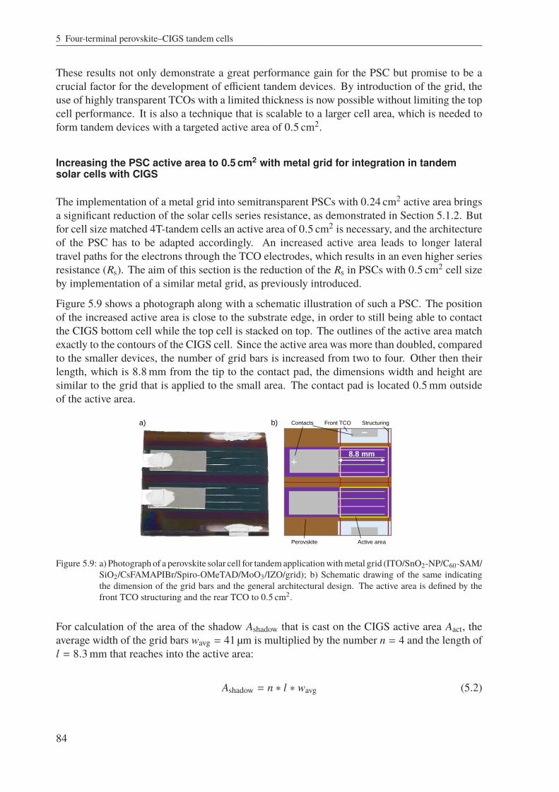
5 Four-terminal perovskite–CIGS tandem cells
These results not only demonstrate a great performance gain for the PSC but promise to be acrucial factor for the development of efficient tandem devices. By introduction of the grid, theuse of highly transparent TCOs with a limited thickness is now possible without limiting the topcell performance. It is also a technique that is scalable to a larger cell area, which is needed toform tandem devices with a targeted active area of 0.5 cm2.
Increasing the PSC active area to 0.5 cm2 with metal grid for integration in tandemsolar cells with CIGS
The implementation of a metal grid into semitransparent PSCs with 0.24 cm2 active area bringsa significant reduction of the solar cells series resistance, as demonstrated in Section 5.1.2. Butfor cell size matched 4T-tandem cells an active area of 0.5 cm2 is necessary, and the architectureof the PSC has to be adapted accordingly. An increased active area leads to longer lateraltravel paths for the electrons through the TCO electrodes, which results in an even higher seriesresistance (Rs). The aim of this section is the reduction of the Rs in PSCs with 0.5 cm2 cell sizeby implementation of a similar metal grid, as previously introduced.
Figure 5.9 shows a photograph along with a schematic illustration of such a PSC. The positionof the increased active area is close to the substrate edge, in order to still being able to contactthe CIGS bottom cell while the top cell is stacked on top. The outlines of the active area matchexactly to the contours of the CIGS cell. Since the active area was more than doubled, comparedto the smaller devices, the number of grid bars is increased from two to four. Other then theirlength, which is 8.8 mm from the tip to the contact pad, the dimensions width and height aresimilar to the grid that is applied to the small area. The contact pad is located 0.5 mm outsideof the active area.
8.8 mm
+
−a) b) Front TCO StructuringContacts
Active areaPerovskite
Figure 5.9: a) Photograph of a perovskite solar cell for tandemapplicationwithmetal grid (ITO/SnO2-NP/C60-SAM/SiO2/CsFAMAPIBr/Spiro-OMeTAD/MoO3/IZO/grid); b) Schematic drawing of the same indicatingthe dimension of the grid bars and the general architectural design. The active area is defined by thefront TCO structuring and the rear TCO to 0.5 cm2.
For calculation of the area of the shadow Ashadow that is cast on the CIGS active area Aact, theaverage width of the grid bars wavg = 41 µm is multiplied by the number n = 4 and the length ofl = 8.3 mm that reaches into the active area:
Ashadow = n ∗ l ∗ wavg (5.2)
84

5.1 Design and performance aspects of four-terminal tandem architectures
The ratio of shaded area in comparison to the active area results in Ashadow/Aact ≈ 2.7 %. Thisfactor can be used for correction of the illumination intensity in measurements such as EQEspectroscopy on CIGS bottom cells with PSC filters applied on top.
For now, the effect of the grid on the PSC photovoltaic performance is evaluated. Figure 5.10shows the statistical results of the characteristic JV values of PSCs with an Aact of 0.24 cm2
and 0.5 cm2 and with and without a metal grid applied to the rear electrode. As expected, thePCE values indicate that the application of the metal grid on the larger cells has an increasinglypositive effect. A mean increase of approximately 3 % in absolute value is observed, comparedto the cells without grid. On smaller area, the gain is limited to only ≈2 %. In this experiment,the maximum PCE values reach about 16 % and 14 % for the 0.24 cm2 and 0.5 cm2 cells,respectively.
468
1012141618
PC
E (
%)
Statistical results from
32 devices
JV-scan direction:
reverse
forward
Box plot legend:
25%~75%
Mean ± 1 SD
Mean
Normal distribution
30405060708090
FF
(%
)
100010501100115012001250
VO
C (
mV
)
16
17
18
19
20
JS
C (
mA
cm
-2)
IZO IZO + Grid IZO IZO + Grid
0.24 cm² 0.5 cm²
-9-6-3036
FH
YS (
%)
Figure 5.10: Box chart of JV-characteristics of perovskite solar cells (ITO/SnO2-NP/C60-SAM/SiO2-NPs/CsFAMAPIBr/Spiro/MoO3/IZO) with different cell sizes and optional Ni-Al-Ni grid.
The performance gain is mainly related to an improved FF, which already indicates an improvedRs, as intended by the grid application. On the one hand, the VOC seems to profit from theenlarged area, but the difference is not statistically significant. On the other hand a loss of up to1 mA cm−2 in average is observed in the JSC on 0.5 cm2. The reason for this may be related toan geometric error in the exact definition of the active area by the sputtered rear electrode. Inaverage, all of the combinations have a FHYS close to zero.
Figure 5.11a displays the JV responses of the best performing PSCs of the experiment. Thesteepness of the diode curves in forward bias direction demonstrates the large effect of the gridand the area of the cell on the conducting properties, hence decreasing the Rs. Comparing the0.5 cm2 cell without grid and the 0.24 cm2 cell with grid, the significant reduction of the FF bythe high Rs is observable.
85
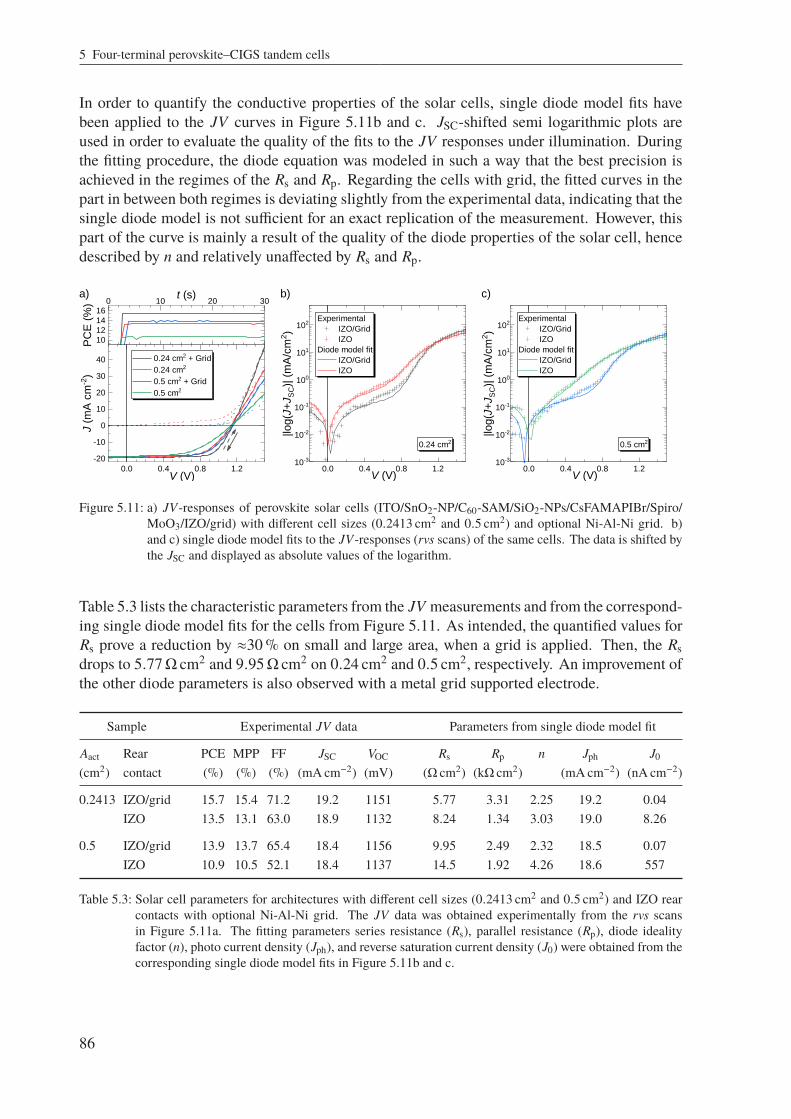
5 Four-terminal perovskite–CIGS tandem cells
In order to quantify the conductive properties of the solar cells, single diode model fits havebeen applied to the JV curves in Figure 5.11b and c. JSC-shifted semi logarithmic plots areused in order to evaluate the quality of the fits to the JV responses under illumination. Duringthe fitting procedure, the diode equation was modeled in such a way that the best precision isachieved in the regimes of the Rs and Rp. Regarding the cells with grid, the fitted curves in thepart in between both regimes is deviating slightly from the experimental data, indicating that thesingle diode model is not sufficient for an exact replication of the measurement. However, thispart of the curve is mainly a result of the quality of the diode properties of the solar cell, hencedescribed by n and relatively unaffected by Rs and Rp.
a) b) c)
0.0 0.4 0.8 1.2
-20
-10
0
10
20
30
40 0.24 cm2 + Grid
0.24 cm2
0.5 cm2 + Grid
0.5 cm2
J (
mA
cm
-2)
V (V)
0 10 20 30
10
12
14
16
t (s)
PC
E (
%)
0.0 0.4 0.8 1.210-3
10-2
10-1
100
101
102
0.24 cm2
Experimental
IZO/Grid
IZO
Diode model fit
IZO/Grid
IZO
|log(J
+J
SC)|
(m
A/c
m2)
V (V)0.0 0.4 0.8 1.2
10-3
10-2
10-1
100
101
102
0.5 cm2
Experimental
IZO/Grid
IZO
Diode model fit
IZO/Grid
IZO
|log(J
+J
SC)|
(m
A/c
m2)
V (V)
Figure 5.11: a) JV-responses of perovskite solar cells (ITO/SnO2-NP/C60-SAM/SiO2-NPs/CsFAMAPIBr/Spiro/MoO3/IZO/grid) with different cell sizes (0.2413 cm2 and 0.5 cm2) and optional Ni-Al-Ni grid. b)and c) single diode model fits to the JV-responses (rvs scans) of the same cells. The data is shifted bythe JSC and displayed as absolute values of the logarithm.
Table 5.3 lists the characteristic parameters from the JV measurements and from the correspond-ing single diode model fits for the cells from Figure 5.11. As intended, the quantified values forRs prove a reduction by ≈30 % on small and large area, when a grid is applied. Then, the Rsdrops to 5.77Ω cm2 and 9.95Ω cm2 on 0.24 cm2 and 0.5 cm2, respectively. An improvement ofthe other diode parameters is also observed with a metal grid supported electrode.
Sample Experimental JV data Parameters from single diode model fit
Aact Rear PCE MPP FF JSC VOC Rs Rp n Jph J0
(cm2) contact (%) (%) (%) (mA cm−2) (mV) (Ω cm2) (kΩ cm2) (mA cm−2) (nA cm−2)
0.2413 IZO/grid 15.7 15.4 71.2 19.2 1151 5.77 3.31 2.25 19.2 0.04IZO 13.5 13.1 63.0 18.9 1132 8.24 1.34 3.03 19.0 8.26
0.5 IZO/grid 13.9 13.7 65.4 18.4 1156 9.95 2.49 2.32 18.5 0.07IZO 10.9 10.5 52.1 18.4 1137 14.5 1.92 4.26 18.6 557
Table 5.3: Solar cell parameters for architectures with different cell sizes (0.2413 cm2 and 0.5 cm2) and IZO rearcontacts with optional Ni-Al-Ni grid. The JV data was obtained experimentally from the rvs scansin Figure 5.11a. The fitting parameters series resistance (Rs), parallel resistance (Rp), diode idealityfactor (n), photo current density (Jph), and reverse saturation current density (J0) were obtained from thecorresponding single diode model fits in Figure 5.11b and c.
86
5.2 Investigation of suitable CIGS bottom cells
The results prove a successful implementation of a Ni-Cu-Ni grid in PSCs with a larger area of0.5 cm2. For tandem devices with CIGS bottom cells this increased area is necessary in order tomatch an equally sized Aact of both sub cells. Additionally, the results indicate how importantthe grid is to maintain a high PCE of the PSC, because otherwise the increase of the active arealeads to significant performance losses, mainly due to a large Rs.
5.2 Investigation of suitable CIGS bottom cells
The aim of this section is to understand the JV response of the CIGS cells, when they areexhibited to a transmission spectrum of a PSC. A simple but sufficiently accurate simulationroutine is developed using a single diode model approach that allows for estimating the PCE, FF,JSC, and VOC of the CIGS cell under a hypothetical PSC transmission spectrum. The simulationroutine may be applied for estimating the CIGS efficiency for a series of fictional transmissionspectra as described in Section 5.4.3 or simply for estimating the theoretical efficiency for realtransmission spectra of PSCs that are too small for tandem measurements and no representativefilters are available as it is done in Section 5.3.
In this process, Section 5.2.1 investigates two different CIGS solar cells that shall be used in thesubsequent experiments in various 4T tandem configurations. Their different architectures areinvestigated focusing on their individual spectral responses and band gaps.
Section 5.2.2 evaluates the CIGS performance under illumination by different PSC transmissionspectra. Furthermore, single diode models are developed that can be used to simulate the JVresponses of the CIGS under filter illumination conditions.
Subsequently, in Section 5.2.3, the models are extended so that the PCEs of the CIGS cells canbe simulated for other hypothetical transmission spectra. This is achieved by using the integratedJSC from the filtered EQE data of the CIGS cell as an input for the single diode model to estimatethe JV response.
5.2.1 CIGS architectures with different band gaps
The CIGS solar cells that are investigated in the following were fabricated by a team of re-searchers at ZSWby thermal co-evaporation under different atmospheric conditions as describedin [121].
This section investigates the setups of two CIGS solar cells, which are used as tandem partners invarious experiments throughout the following sections. Figure 5.12 shows SEM cross sectionsof two different CIGS absorber layers that have different gallium content.
87

5 Four-terminal perovskite–CIGS tandem cells
2 µm 2 µmMolybdenum
CIGS
MgF2
ZAO
ZMO
CdS
a) CIGSa b) CIGSb
Figure 5.12: Cross sectional SEM images of a) a complete high efficiency CIGS solar cell and b) a CIGS cell witha low gallium content before buffer and window layer deposition.
The SEM images show that the absorber layer of both samples have a different thickness andmorphology. Designed for high PCE in solo applications, the CIGS cell in Figure 5.12a (CIGSa)has a engineered gallium gradient along the comparably thick absorber layer. The buffer layercadmium sulfide (CdS) and the window layers zinc magnesium oxide ZnxMg1– xO (ZMO) andZAO have a optimized thickness for low parasitic absorption and the use of a metal grid.Additionally, an ARC of magnesium fluoride (MgF2) has been applied for better optical yield.The CIGS layer in Figure 5.12b (CIGSb) is thinner and has a very low gallium content in orderto reduce the Eg. The buffer and window layers are not shown in the image.
Table 5.4 lists the thicknesses of all layers of the two final CIGS cell architectures. It shows thatCIGSb comprises intrinsic zinc oxide (i-ZnO) instead of ZMO and uses a larger ZAO and CdSlayer thickness than CIGSa.
Layer CIGSa CIGSb
d d(nm) (nm)
MgF2 113 -ZAO 145 420ZMO 50 -i-ZnO - 90CdS 24 50CIGS 3070 2340Mo 570 510
Table 5.4: Layer thickness values of the solar cell architectures of CIGS cell with Eg = 1.1 eV (CIGSa) and CIGScell with Eg = 1.0 eV (CIGSb).
88

5.2 Investigation of suitable CIGS bottom cells
The Eg of the CIGS cells can be adjusted by variation of the gallium to indium ratio (GGI). Anengineered GGI gradient along the depth of the CIGS layer is generally used to optimise thesolar cell performance. [122] The glow discharge optical emission spectroscopy (GDOES) datain Figure 5.13 reveals that the GGI ratio of CIGSa varies between 0.2 at the front and 0.5 at theback with a minimum of 0.15. The GGI profile of CIGSb is comparably flat and the Ga contentis nearly zero in the front. As the minimum of the GGI reflects also the minimum of the Eg, itis decisive for the overall absorption range of the CIGS solar cell.
0.0 0.2 0.4 0.6 0.8 1.00.0
0.1
0.2
0.3
0.4
0.5
[Ga]/
([G
a]+
[In])
normalised layer depth
CIGSa
CIGSb
Figure 5.13: Experimental data from GDOES: GGI ratios as functions of the normalized CIGS layer depth of thehigh efficiency CIGS solar cell (CIGSa) and a CIGS cell with a low gallium content (CIGSb).
Having a much lower GGI minimum, the absorption range of CIGSb is extended up to ≈1300 nmas demonstrated in the EQE data in Figure 5.14a compared to CIGSa, which absorbs only up to≈1150 nm. Furthermore, the relatively lower EQE of CIGSb especially in the range of 300 nmto 450 nm results from the increased parasitic absorption of the comparably thicker ZAO andCdS layers.
In order to determine the Eg of both cells from the EQE, two approaches are chosen here. Thefirst method, introduced by Helmers et al. [123], is based on an exponential relationship betweenthe absorption coefficient (α) and the photon energy (hν) (Urbach’s rule) [124–126]
α ∝ exp(σhνkT
), (5.3)
with the Boltzmann constant (k), the temperature (T) and a dimensionless steepness parameter(σ). The second method involves the square root relationship between α and Eg of a direct bandtransition (Tauc relation) [127, 128], which was originally developed for amorphous materialsbut has proven to be also accurate for crystalline materials: [129]
hν · α ∝√
hν − Eg . (5.4)
Assuming a sufficiently good absorption at the band edge and a sufficient diffusion length, whichis the case for CIGS, the absorption coefficient is directly proportional to the EQE. [130]
89

5 Four-terminal perovskite–CIGS tandem cells
Hence, following equation 5.3 the onset of the EQE exhibits an exponential behaviour in Figure5.14b and saturates close to unity above Eg. As stated in ref. [123], the Eg is determined bythe transition from the onset to the saturation regime, by fitting two exponential functions ofthe form exp(a + b · hν) to the corresponding regimes and extracting Eg from their intersection,marked by a sphere symbol.
Using the Tauc relation from eq. 5.4, the linear regions in the (hν · EQE)2 versus hν plots inFigure 5.14c are interpolated to derive the Eg from the intersection with the abscissa axis.
1.00 1.05 1.10 1.15 1.200
(hn × E
QE
)2
hn (eV)
CIGSa
CIGSb
Eg = 1.10 eVEg = 1.00 eV
b) c)a)
1.0 1.2 1.410-3
10-2
10-1
100
Eg = 1.09 eV Eg = 1.01 eVE
QE
hn (eV)
CIGSa
direct
saturation
1.0 1.2 1.4
CIGSb
direct
saturation
400 600 800 1000 12000
20
40
60
80
100
EQ
E (
%)
wavelength (nm)
CIGSa
CIGSb
Figure 5.14: a) EQE responses of CIGSa and CIGSb; The Eg is determined from the EQE by two methods: b) Inthe semilogarithmic plots of the EQEs versus hν Eg is derived from the intersection of two exponentialfits, one at the onset of the EQE and one in the saturation region. c) In the (hν · EQE)2 versus hν plotsEg is determined from the intersections of the linear interpolations with the abscissa axis.
Both methods for determining the Eg give similar results with low deviations of <10 meV.According to the results CIGSa has a Eg of 1.1 eV and CIGSb with the low gallium content hasa Eg of 1.0 eV, which is comparable to the Eg of pure CIS.
5.2.2 CIGS bottom cell performance estimations from single diode models
This section investigates the two CIGS cells with the band gaps of 1.1 eV and 1.0 eV, whichwere introduced in the previous Section 5.2.1. Their JV performance is measured under the fullAM1.5G solar spectrum and under the transmission spectra of two different perovskite filters.The filters have equal layer stacks despite different front electrodes. The one comprises a highlyNIR transparent IO:H electrode and the other has a less transparent ITO electrode in order tosimulate significant changes in the transmitted spectrum. The spectral differences are used toinvestigate how the diode behaviour of the CIGS is affected.
In order to create simple and accurate simulation routines that can predict the JV respsonses ofthe two CIGS cells in these tandem configurations, single diode models are developed that usethe input parameters Rs, Rp, n and J0 from direct fits to these measurements. The JSC value canbe integrated from filtered EQE data using the transmission data of the PSC which is discussedin more detail in the subsequent section 5.2.3. From this set of model parameters the CIGS cellscharacteristic values PCE, FF, VOC, and JSC can be calculated using the model.
Hence, the results of the measurements and fits are plotted in Figure 5.15 for determination ofthe fitting parameters Rs, Rp, n, and J0.
90

5.2 Investigation of suitable CIGS bottom cells
-0.2 0.0 0.2 0.4 0.6 0.8
-40
-30
-20
-10
0
10
20
30
40
J (
mA
cm
-2)
V (V)
Experimental
CIGSa (1.1 eV)
+ PSC Filter (ITO)
+ PSC Filter (IOH)
Diode model
CIGSa (1.1 eV)
+ PSC Filter (ITO)
+ PSC Filter (IOH)
-0.2 0.0 0.2 0.4 0.6 0.8
-40
-30
-20
-10
0
10
20
30
40Experimental
CIGSb (1.00 eV)
+ PSC Filter (ITO)
+ PSC Filter (IOH)
Diode model
CIGSb (1.00 eV)
+ PSC Filter (ITO)
+ PSC Filter (IOH)
J (
mA
cm
-2)
V (V)
a) b)
Figure 5.15: a) Experimental JV data of a CIGS cell with Eg = 1.1 eV (CIGSa) measured without a filter (solo)and filtered by PSCs with different front TCOs (ITO and IO:H). The solid lines represent singlediode model fits of the three cases. b) JV data and single diode model fits of a CIGS cell withEg = 1.0 eV (CIGSb) under the same conditions.
In general, the individual fits show a very good accordance with the experimental data. Asintended, the filters absorb a large proportion of the light, so that the photocurrent of the CIGSis reduced. Since the perovskite filters themselves have a different transmittance, the currentgenerated by the filtered CIGS cells varies significantly. Especially the CIGS cell with thesmaller Eg of 1.0 eV (Figure 5.15b), hence broader absorption range, gains more current fromthe increased NIR transmittance of the PSC filter with the IO:H front electrode (blue line),compared to the PSC with ITO (red line).
Table 5.5 lists the experimental data from the JV measurements and the fitting parameters forthe two investigated CIGS cells under the different illumination conditions.
Sample Experimental JV Data Parameters from single diode model fit
ID Filter PCE FF JSC VOC Rs Rp n Jph J0 FF PCE(%) (%) (mA cm−2) (V) (Ω cm2) (kΩ cm2) (mA cm−2) (nA cm−2) (%) (%)
CIGSa solo 22.13 79.4 38.8 0.72 0.28 17.3 1.40 38.8 0.09 79.3 22.13ITO 6.85 78.0 13.2 0.66 0.59 14.4 1.44 13.2 0.23 78.0 6.84IO:H 8.04 78.0 15.4 0.67 0.57 14.3 1.45 15.4 0.25 77.9 8.03
CIGSb solo 15.61 76.3 37.5 0.55 0.25 2.3 1.27 37.5 1.95 76.4 15.64ITO 5.27 75.3 13.6 0.51 0.32 2.3 1.24 13.6 1.29 75.9 5.31IOH 6.58 75.5 16.8 0.52 0.31 2.3 1.25 16.8 1.55 76.0 6.62
Table 5.5: Experimental JV data and parameters of the corresponding single diode model fits for a CIGS cell withEg = 1.1 eV (CIGSa) and CIGSb measured without a filter (solo) and filtered by PSCs with differentfront TCOs (ITO and IO:H).
A difference of the diode parameters is observed comparing the filtered and unfiltered CIGScells. Especially the fitting parameters Rp, Rs, and J0 show large deviations under filteredconditions. This is true for both types of CIGS with different band gaps. The variations canbe explained by the different charge carrier generation profiles along the depth of the CIGS cellunder the changing spectral conditions.
91

5 Four-terminal perovskite–CIGS tandem cells
However, it is also observed that the fitting parameters for the filtered JV curves prove to bevery similar between the two types of applied filters. Hence, the set of fitting parameters forthe simulation routines is determined for the two CIGS cells, resulting in the average values inTable 5.6. With these sets of parameters JV curves for the filtered CIGSa and CIGSb cells canbe simulated from the implicit single diode model equation 5.5 using the Jph as an additionalinput. One benefit of using the single diode model approach is that it allows for an iterativenumerical calculation of the solar cell parameters PCE, FF, VOC and JSC. [131, 132]
J = J0 ·
[exp
(V − J · Rsn · kT/q
)− 1
]+
V − J · RsRp
− Jph (5.5)
Sample Parameters for single diode model simulation
ID Rs Rp n J0
(Ω cm2) (kΩ cm2) (pA cm−2)
CIGSa 0.58 14.35 1.45 237CIGSb 0.32 2.27 1.24 1422
Table 5.6: Parameters for the single diode model simulations for CIGS cell with Eg = 1.1 eV (CIGSa) and CIGSbas bottom cells under filter conditions.
For validation of the equations the coefficient of determination (R2) is reviewed for the fourtandem setups, using the experimental JSC values for Jph in the calculation of the JV curvemodels. The residual results and the experimental PCEf and simulated PCESim values are listedin Table 5.7 and indicate that both models achieve a very high accuracy in all cases with a R2 ofover 0.995 and a close match of the PCE.
Sample Experimental Single diode model
ID Eg Filter PCEf PCESim R2
(eV) (%) (%)
CIGSa 1.1 ITO 6.85 6.85 1.000IO:H 8.04 8.03 0.9995
CIGSb 1.0 ITO 5.27 5.28 0.9966IOH 6.58 6.61 0.9988
Table 5.7: Comparison of the experimental PCE data of filtered CIGSa and CIGSb with the simulated valuesobtained by the single diode models. The CIGS cells are filtered by PSCs with different front TCOs(ITO and IO:H). R2 denotes the coincidence of the experimental and simulated JV curve.
The single diode models for CIGSa and CIGSb can be used to precisely determine the perfor-mance of these cells in a hypothetical tandem setup under two conditions: (i) the photo currentdensity (Jph) of the filtered CIGS is known and (ii) the illumination spectrum matches roughlywith the transmitted spectrum of the perovskite filters.
92
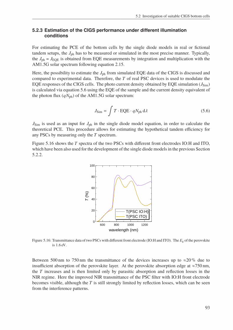
5.2 Investigation of suitable CIGS bottom cells
5.2.3 Estimation of the CIGS performance under different illuminationconditions
For estimating the PCE of the bottom cells by the single diode models in real or fictionaltandem setups, the Jph has to be measured or simulated in the most precise manner. Typically,the Jph = JEQE is obtained from EQE measurements by integration and multiplication with theAM1.5G solar spectrum following equation 2.15.
Here, the possibility to estimate the Jph from simulated EQE data of the CIGS is discussed andcompared to experimental data. Therefore, the T of real PSC devices is used to modulate theEQE responses of the CIGS cells. The photo current density obtained by EQE simulation (JSim)is calculated via equation 5.6 using the EQE of the sample and the current density equivalent ofthe photon flux (qNph) of the AM1.5G solar spectrum:
JSim =∫
T · EQE · qNph dλ (5.6)
JSim is used as an input for Jph in the single diode model equation, in order to calculate thetheoretical PCE. This procedure allows for estimating the hypothetical tandem efficiency forany PSCs by measuring only the T spectrum.
Figure 5.16 shows the T spectra of the two PSCs with different front electrodes IO:H and ITO,which have been also used for the development of the single diodemodels in the previous Section5.2.2.
600 800 1000 12000
20
40
60
80
100
T (
%)
wavelength (nm)
T(PSC IO:H)
T(PSC ITO)
Figure 5.16: Transmittance data of two PSCswith different front electrode (IO:H and ITO). The Eg of the perovskiteis 1.6 eV.
Between 500 nm to 750 nm the transmittance of the devices increases up to ≈20 % due toinsufficient absorption of the perovskite layer. At the perovskite absorption edge at ≈750 nm,the T increases and is then limited only by parasitic absorption and reflection losses in theNIR regime. Here the improved NIR transmittance of the PSC filter with IO:H front electrodebecomes visible, although the T is still strongly limited by reflection losses, which can be seenfrom the interference patterns.
93

5 Four-terminal perovskite–CIGS tandem cells
By multiplication of the T spectra of the filters with the EQE responses of the previouslyintroduced CIGS cells (CIGSa and CIGSb with Eg =1.1 eV and 1.0 eV, respectively) underillumination of the AM1.5G solar spectrum, Figure 5.17 shows the simulated EQE as theywould appear in the actual tandem configuration. For comparison, also the experimental EQEof the CIGS cells is shown, when the cells are filtered by the two real PSC devices, denoted asPSC-IO:H and PSC-ITO.
a) b)
400 600 800 1000 12000
20
40
60
80
100
EQ
E (
%)
wavelength (nm)
Experimental
CIGSa solo (1.1 eV)
CIGSa + PSC-IO:H
CIGSa + PSC-ITO
Simulated
T(PSC-IO:H) × EQE solo
T(PSC-ITO) × EQE solo
400 600 800 1000 12000
20
40
60
80
100
EQ
E (
%)
wavelength (nm)
Experimental
CIGSb solo (1.0 eV)
CIGSb + PSC-IO:H
CIGSb + PSC-ITO
Simulated
T(PSC-IO:H) × EQE solo
T(PSC-ITO) × EQE solo
Figure 5.17: a) Experimental EQE data (+) of a CIGS cell with an Eg of 1.1 eV under the AM1.5G solar spectrum(solo) and under two PSC filters with different front electrode (IO:H and ITO). The simulated EQEdata (—) is obtained from multiplication of the EQE with transmittance data from Figure 5.16. b)Similar data for a CIGS cell with an Eg of 1.0 eV.
Comparing the experimental and simulated EQE responses of the two CIGS cells in Figure5.17a and b, the simulated curves seem to underestimate the quantum efficiency to some extent,especially in the regimes of the interference maxima, where most light is transmitted. This effectis reasoned by the additional back reflection of light at the PSC that got partially reflected fromthe CIGS bottom cells surface in the first place. In experiment, this double back reflection takesplace naturally, increasing the quantum efficiency of the bottom cell. But when using only theT spectrum as an input for the EQE simulation, the additional amount of back reflected light isneglected.
Since the double back reflection is dependent on T and the refractive indices of all contributinglayers in the tandem stack, this effect cannot be easily included in this simple simulation approach.However, by calculating the mismatch between experiment and simulation, the error introducedby this effect can be estimated and respected in the simulations for the fictional PSC filters.When calculating the JEQE from the measured and JSim from the simulated EQE responses withthe filters PSC-IO:H and PSC-ITO applied, the maximum relative errors summarise to <3.5 %and <2.5 % for the two CIGS cells with Eg =1.1 eV and 1.0 eV, respectively.
The calculated JSim and JEQE values for the different scenarios are used to estimate the corre-sponding PCE of the CIGS cells according to the single diode model equation 5.1. Figure 5.18summarises the PCE results for both cells CIGSa and CIGSb as a function of the Jph. The filtersetups used in the calculation are colour coded and denoted accordingly. Additionally the graphcontains the experimental PCE and JSC values obtained from regular JV measurements for bothCIGS cells with the PSC-IO:H and PSC-ITO filters applied.
94
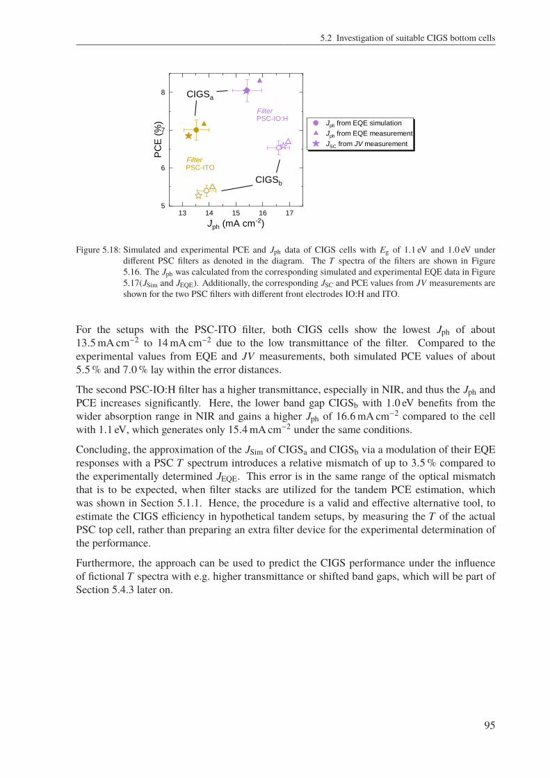
5.2 Investigation of suitable CIGS bottom cells
13 14 15 16 175
6
7
8
PSC-IO:H
PSC-ITOFilter
Filter
CIGSb
PC
E (
%)
Jph (mA cm-2)
Jph from EQE simulation
Jph from EQE measurement
JSC from JV measurement
CIGSa
Figure 5.18: Simulated and experimental PCE and Jph data of CIGS cells with Eg of 1.1 eV and 1.0 eV underdifferent PSC filters as denoted in the diagram. The T spectra of the filters are shown in Figure5.16. The Jph was calculated from the corresponding simulated and experimental EQE data in Figure5.17(JSim and JEQE). Additionally, the corresponding JSC and PCE values from JV measurements areshown for the two PSC filters with different front electrodes IO:H and ITO.
For the setups with the PSC-ITO filter, both CIGS cells show the lowest Jph of about13.5 mA cm−2 to 14 mA cm−2 due to the low transmittance of the filter. Compared to theexperimental values from EQE and JV measurements, both simulated PCE values of about5.5 % and 7.0 % lay within the error distances.
The second PSC-IO:H filter has a higher transmittance, especially in NIR, and thus the Jph andPCE increases significantly. Here, the lower band gap CIGSb with 1.0 eV benefits from thewider absorption range in NIR and gains a higher Jph of 16.6 mA cm−2 compared to the cellwith 1.1 eV, which generates only 15.4 mA cm−2 under the same conditions.
Concluding, the approximation of the JSim of CIGSa and CIGSb via a modulation of their EQEresponses with a PSC T spectrum introduces a relative mismatch of up to 3.5 % compared tothe experimentally determined JEQE. This error is in the same range of the optical mismatchthat is to be expected, when filter stacks are utilized for the tandem PCE estimation, whichwas shown in Section 5.1.1. Hence, the procedure is a valid and effective alternative tool, toestimate the CIGS efficiency in hypothetical tandem setups, by measuring the T of the actualPSC top cell, rather than preparing an extra filter device for the experimental determination ofthe performance.
Furthermore, the approach can be used to predict the CIGS performance under the influenceof fictional T spectra with e.g. higher transmittance or shifted band gaps, which will be part ofSection 5.4.3 later on.
95
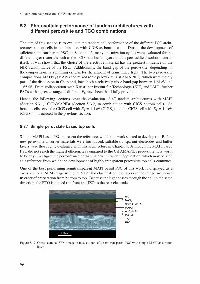
5 Four-terminal perovskite–CIGS tandem cells
5.3 Photovoltaic performance of tandem architectures withdifferent perovskite and TCO combinations
The aim of this section is to evaluate the tandem cell performance of the different PSC archi-tectures as top cells in combination with CIGS as bottom cells. During the development ofefficient semitransparent PSCs in Section 4.3, many optimization cycles were evaluated for thedifferent layer materials such as the TCOs, the buffer layers and the perovskite absorber materialitself. It was shown that the choice of the electrode material has the greatest influence on theNIR transmittance of the PSC. Additionally, the band gap of the perovskite, depending onthe composition, is a limiting criteria for the amount of transmitted light. The two perovskitecompositions MAPbI3 (MAPI) and mixed ionic perovskite (CsFAMAPIBr), which were mainlypart of the discussion in Chapter 4, have both a relatively close band gap between 1.61 eV and1.65 eV. From collaboration with Karlsruher Institut für Technologie (KIT) and LMU, furtherPSCs with a greater range of different Eg have been thankfully provided.
Hence, the following sections cover the evaluation of 4T tandem architectures with MAPI(Section 5.3.1), CsFAMAPIBr (Section 5.3.2) in combination with CIGS bottom cells. Asbottom cells serve the CIGS cell with Eg = 1.1 eV (CIGSa) and the CIGS cell with Eg = 1.0 eV(CIGSb), introduced in the previous section.
5.3.1 Simple perovskite based top cells
Simple MAPI based PSC represent the reference, which this work started to develop on. Beforenew perovskite absorber materials were introduced, suitable transparent electrodes and bufferlayers were thoroughly evaluated with this architecture in Chapter 4. Although the MAPI basedPSC did not reach the highest efficiencies compared to the CsFAMAPIBr perovskite, it is worthto briefly investigate the performance of this material in tandem application, which may be seenas a reference from which the development of highly transparent perovskite top cells continues.
One of the best performing semitransparent MAPI based PSC of this work is displayed as across sectional SEM image in Figure 5.19. For clarification, the layers in the image are shownin order of preparation from bottom to top. Because the light passes through the cell in the samedirection, the FTO is named the front and IZO as the rear electrode.
500 nm
IZO
Spiro-OMeTAD
MoO3
MAPbI3
TiO2
FTO
Al2O3-NPs
PCBM
Figure 5.19: Cross sectional SEM image in false colours of a semitransparent PSC with simple MAPI absorptionlayer.
96
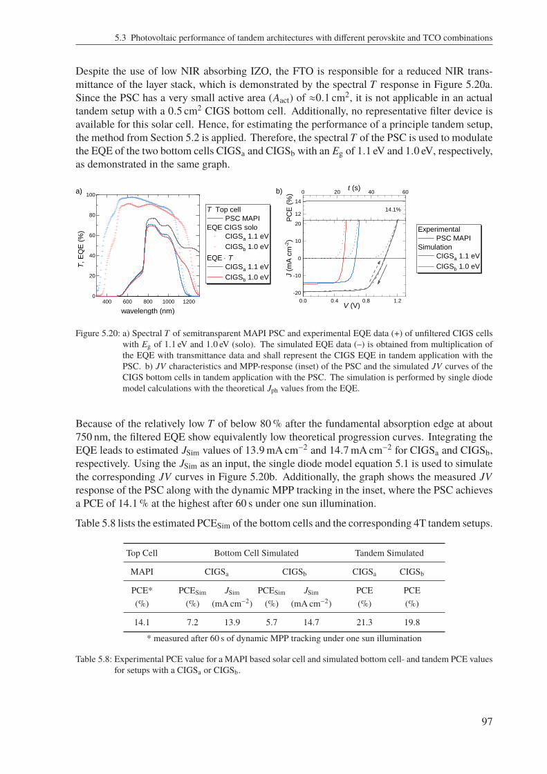
5.3 Photovoltaic performance of tandem architectures with different perovskite and TCO combinations
Despite the use of low NIR absorbing IZO, the FTO is responsible for a reduced NIR trans-mittance of the layer stack, which is demonstrated by the spectral T response in Figure 5.20a.Since the PSC has a very small active area (Aact) of ≈0.1 cm2, it is not applicable in an actualtandem setup with a 0.5 cm2 CIGS bottom cell. Additionally, no representative filter device isavailable for this solar cell. Hence, for estimating the performance of a principle tandem setup,the method from Section 5.2 is applied. Therefore, the spectral T of the PSC is used to modulatethe EQE of the two bottom cells CIGSa and CIGSb with an Eg of 1.1 eV and 1.0 eV, respectively,as demonstrated in the same graph.
400 600 800 1000 12000
20
40
60
80
100
T,
EQ
E (
%)
wavelength (nm)
T Top cell
PSC MAPI
EQE CIGS solo
CIGSa 1.1 eV
CIGSb 1.0 eV
EQE × T
CIGSa 1.1 eV
CIGSb 1.0 eV
14.1%
0.0 0.4 0.8 1.2
-20
-10
0
10
20Experimental
PSC MAPI
Simulation
CIGSa 1.1 eV
CIGSb 1.0 eV
J (
mA
cm
-2)
V (V)
0 20 40 60
12
14
t (s)
PC
E (
%)a) b)
Figure 5.20: a) Spectral T of semitransparent MAPI PSC and experimental EQE data (+) of unfiltered CIGS cellswith Eg of 1.1 eV and 1.0 eV (solo). The simulated EQE data (–) is obtained from multiplication ofthe EQE with transmittance data and shall represent the CIGS EQE in tandem application with thePSC. b) JV characteristics and MPP-response (inset) of the PSC and the simulated JV curves of theCIGS bottom cells in tandem application with the PSC. The simulation is performed by single diodemodel calculations with the theoretical Jph values from the EQE.
Because of the relatively low T of below 80 % after the fundamental absorption edge at about750 nm, the filtered EQE show equivalently low theoretical progression curves. Integrating theEQE leads to estimated JSim values of 13.9 mA cm−2 and 14.7 mA cm−2 for CIGSa and CIGSb,respectively. Using the JSim as an input, the single diode model equation 5.1 is used to simulatethe corresponding JV curves in Figure 5.20b. Additionally, the graph shows the measured JVresponse of the PSC along with the dynamic MPP tracking in the inset, where the PSC achievesa PCE of 14.1 % at the highest after 60 s under one sun illumination.
Table 5.8 lists the estimated PCESim of the bottom cells and the corresponding 4T tandem setups.
Top Cell Bottom Cell Simulated Tandem Simulated
MAPI CIGSa CIGSb CIGSa CIGSb
PCE* PCESim JSim PCESim JSim PCE PCE(%) (%) (mA cm−2) (%) (mA cm−2) (%) (%)
14.1 7.2 13.9 5.7 14.7 21.3 19.8
* measured after 60 s of dynamic MPP tracking under one sun illumination
Table 5.8: Experimental PCE value for a MAPI based solar cell and simulated bottom cell- and tandem PCE valuesfor setups with a CIGSa or CIGSb.
97

5 Four-terminal perovskite–CIGS tandem cells
As a result, the CIGS cell with Eg = 1.1 eV (CIGSa) retains only about 7.2 % in PCESim bycalculation of the performance with the single diode model and the T of the PSC (iv). Becausethe loss in PCESim accounts for nearly 15 % absolute compared to the solo PCE of 21.1 %, thehypothetical tandem device of the PSC and CIGSa would have a summarized PCE of 21.3 %,which is even lower than the solo PCE of CIGSa.
With the extended absorption range, the CIGS cell with Eg = 1.0 eV (CIGSb) is able to achieve ahigher JSim than CIGSa. Despite that the resulting PCESim from the filtered single diode modelcalculation is only as high as 5.7 %, the loss compared to the solo PCE is only about 10 % inabsolute values. This raises the theoretical tandem setup PCE of 19.8 % above both single cellPCEs of 15.6 % in solo application (compare Table 5.5).
The results demonstrate that for high efficiency CIGS cells, also very good performing PSC cellsare needed in order to make the tandem setup having a better PCE than each of the sub cells. Agood performing PSC does not only demand a high PCE but a very good NIR transmittance.
5.3.2 Multi cation perovskite based top cells
A higher tandem efficiency is expected from the use of the CsFAMAPIBr perovskite absorbermaterial in the top cell, compared to simple MAPI. The multi cation approach has proven mainadvantages in power conversion efficiency and hysteresis as discussed in Chapter 4, which woulddirectly benefit the tandem performance. In Figure 5.21 the Eg of CsFAMAPIBr is determinedto be ≈1.62 eV, which is similar to MAPI [27], hence no band gap related gain is expectedfor the bottom cell performance. However, the transmittance of the semitransparent PSCs withCsFAMAPIBr could be significantly increased with the introduction of low NIR absorbing TCOelectrodes in Section 4.3.2, which promises great potential in tandem application.
Therefore, this chapter evaluates the performance of tandem architectures with CsFAMAPIBrbased PSCs and CIGS focusing on the use of different TCO combinations for the electrodes.The discussion is divided into two sections. Firstly, the variety of combinations is comparedby tandem efficiency estimations with different PSC filters. Secondly, a selection of the mostpromising setups is evaluated in actual tandem devices with PSC and CIGS cells of the samecell size.
Estimation of tandem device PCEs with PSC filters
Semitransparent PSC with a high transmittance (T) in the NIR regime are mandatory for awell performing bottom cell in tandem applications. The absorptance (A) of the PSC could besignificantly reduced in the NIR with the introduction of IO:H and IZO as electrodes, but higherPCEs values were achieved with the traditional TCO, such as ITO. The question of which resultsin a better tandem performance is about to be discussed in the following.
For evaluation of the bottom cell performance, a set of perovskite filters is prepared that is usedto estimate the PCEf of the CIGS cells in different possible tandem setups via simulations orexperiments. The performance data of the top cell setups is collected from various experiments,comprising the best performing PSC with similar architectures to the filters. All of the PSCshave an Aact of 0.24 cm2, some are equipped with an optional metal grid at the rear electrode.Finally the tandem PCE is estimated from the sum of the PCEs of each sub cell.
98

5.3 Photovoltaic performance of tandem architectures with different perovskite and TCO combinations
1.55 1.60 1.65 1.70 1.75
PSC with CsFAMAPIBr
linear regression
(ahn)2
hn (eV)
Eg = 1.623 eV
Figure 5.21: Tauc plot (αhν)2 versus hν for a PSC with CsFAMAPIBr perovskite absorber material for determiningthe Eg.
Figure 5.22a shows the T of the set of PSC filters with the architecture glass/front electrode/SnO2-NP/C60-SAM/SiO2-NPs/CsFAMAPIBr/Spiro-OMeTAD/MoO3/rear electrode. They in-corporate FTO, ITO, IZO and PDC–IO:H as front electrodes and IZO or a-IO:H in place ofthe rear electrodes. The graph in Figure 5.22b depicts the integral curve of the current densityequivalent of the transmission (JTrn) of the same setups, following equation 2.12.
As expected, the filters with the PDC–IO:H and IZO front electrodes have a superiorT comparedto ITO and FTO. The interference modulations of the T spectra make a direct comparison ofthe closely related curves with the same front TCO and different rear TCOs difficult. Hence, theintegral curves of the JTrn reveal that the filters with the IZO rear contact accumulate a smalladvantage over the ones with a-IO:H in the range up to 1200 nm.
600 800 1000 12000
20
40
60
80
100
T (
%)
Wavelength (nm)
800 900 1000 1100 1200 13000
2
4
6
8
10
12
14
16
18
20
22
24
Inte
gra
ted J
Trn
(m
A c
m-2
)
Wavelength (nm)
Colour: Front TCO
FTO ITO
IZO PDC-IO:H
Style: Rear TCO
a-IO:H IZO
a) b)
Figure 5.22: a) Spectral transmittance (T) and b) integrated current density equivalent of the transmission (JTrn)versus wavelength of different PSC filters, representing complete semitransparent solar cells based onCsFAMAPIBr perovskite. The filter stacks comprise a variation of front electrodes (colour coded:FTO, ITO, IZO, and PDC–IO:H) as well as different rear electrodes (solid: a-IO:H; dashed: IZO).
99

5 Four-terminal perovskite–CIGS tandem cells
Using the T of the PSC filters as the input, the estimated JSC and PCESim values are simulatedvia the single diode model for the two different bottom cells CIGSa and CIGSb (see Section5.2). The results are listed in Table 5.9 along with the PCEs of the best performing PSCscorresponding to each filter architecture. For CIGSa the experimental data is also shown andthe PCEf of the hypothetical tandem setups is estimated. An additional correction was used forthe tandem estimation of PSC samples with a grid. The JSC of the bottom cell was reducedaccording to a shadowing factor of 2.7 %, as it was calculated in 5.1.2 for the PSC metal gridthat is used in cells with matching active area.
Experimental Values Top Cell Experimental Values CIGSa Simulated Values CIGSa Simulated Values CIGSb
Perovskite Solar Cell Data Filter Data Filter + CIGSa Tandem Filter + CIGSa Tandem Filter + CIGSb Tandem
Electrodes PCE* Twt** JTrn*** JSC PCEf PCE JSim PCESim PCE JSim PCESim PCEFront Rear (%) (%) (mA cm−2) (mA cm−2) (%) (%) (mA cm−2) (%) (%) (mA cm−2) (%) (%)
FTO a-IO:H 13.70 62.80 19.09 13.97 7.30 21.00 14.04 7.29 20.99 14.84 5.80 19.50IZO 13.00 63.01 19.04 14.20 7.37 20.37 14.20 7.38 20.38 14.92 5.83 18.83
ITO a-IO:H 15.10 57.81 18.20 13.49 6.97 22.07 13.50 7.00 22.10 14.15 5.50 20.60IZO 14.30 57.93 18.26 13.65 7.14 21.44 13.78 7.15 21.45 14.29 5.57 19.87a-IO:H + Grid+ 15.50 56.25 17.70 13.12 6.78 22.28 13.14 6.80 22.30 13.77 5.34 20.84IZO + Grid+ 16.60 56.37 17.77 13.29 6.95 23.55 13.41 6.94 23.54 13.91 5.40 22.00
IZO a-IO:H 14.10 74.34 22.34 15.68 8.20 22.30 15.79 8.26 22.36 16.95 6.69 20.79IZO 12.70 73.22 22.04 15.82 8.23 20.93 15.84 8.28 20.98 16.87 6.66 19.36
PDC-IO:H a-IO:H 14.90 77.19 22.85 15.73 8.25 23.15 15.81 8.27 23.17 17.17 6.78 21.68IZO 13.20 77.14 22.85 15.87 8.35 21.55 16.01 8.38 21.58 17.28 6.83 20.03a-IO:H + Grid+ 14.50 75.10 22.23 15.30 8.03 22.53 15.39 8.04 22.54 16.70 6.58 21.08IZO + Grid+ 15.40 75.05 22.23 15.45 8.12 23.52 15.58 8.14 23.54 16.81 6.63 22.03
* PCE after 30 s of dynamic MPP tracking under one sun illumination** Twt in the NIR range between 800 nm to 1300 nm
*** JTrn in the range 300 nm to 1300 nm+ all values are corrected for a grid shadow area of 2.7 %
Table 5.9: Experimental values of the top cell: PCEs of the best performing PSC devices with Aact of 0.24 cm2 anddifferent combinations of front and rear electrodes. Equivalent PSC filters with larger area shall representthe corresponding transmission behaviour, given in terms of weighted average transmittance (Twt) andcurrent density equivalent of the transmission (JTrn).Experimental values of CIGSa: measured JSC and PCEf of CIGSa when the PSC filter is stacked on top.The tandem PCE denotes the cumulative efficiency of PSC and the filtered CIGS.Simulated values of CIGSa and CIGSb: simulated JSim and PCESim of CIGSa and CIGSb, where JSimis obtained via equation 5.6 and used for calculation of the PCESim via the single diode models fromSection 5.2.2. The tandem PCE denotes the cumulative efficiency of PSC and the simulated CIGS.Since the PSC filters do not have a grid, the grid shading factor of 2.7 % (see Section 5.1.2) is used forestimation of the losses in Twt and JTrn of the filter and the JSC, JSim and PCE values of the CIGS cells.
The results indicate that both a high PCE or high T of the PSC can lead to the highest tandemPCEs. 23.5 % is the best theoretical tandem PCE, which is simultaneously achieved by twodifferent setups each with CIGSa as the bottom cell. One setup comprises a PSC with ITO front-and IZO+grid rear electrode, achieving a PCE of 16.6 % and a weighted average transmittance(Twt) of 56.2 %. The other setup uses PDC–IO:H as a front electrode, which increases the Twtto 75.1 % at a PCE of 15.4 %.
As the bottom cell PCESim (or PCEf) represents a direct measure for the transmission quality ofthe top cell, the CIGS PCESim vs. PSC PCE data plot in Figure 5.23 effectively visualises thecorrelation matrix between top cell transmittance, top cell PCE and tandem PCE.
100

5.3 Photovoltaic performance of tandem architectures with different perovskite and TCO combinations
1
3
5
7
9 11
2
4
6
8
1012
1
3
5
7
911
2
4
6
8
1012
6.5
7.0
7.5
8.0
8.5
23.5
24.0
24.5
25.0
25.5
19
2021 22
23
24
Estim
ate
d T
andem
PC
E (
%)
Filt
ere
d C
IGS
PC
E (
%)
CIGSa
grid
grid
grid
PSCb
PSCa
PSCb
PSC front - rear electrode
1 - ITO - a-IO:H/grid
2 - ITO - IZO/grid (PSCb)
3 - PDC-IO:H - a-IO:H/grid
4 - PDC-IO:H - IZO/grid (PSCa)
5 - FTO - a-IO:H
6 - FTO - IZO
7 - ITO - a-IO:H
8 - ITO - IZO
9 - IZO - a-IO:H
10 - IZO - IZO
11 - PDC-IO:H - a-IO:H
12 - PDC-IO:H - IZO
Experimental data
PSCa
12 13 14 15 16 175.0
5.5
6.0
6.5
7.0
22.0
22.5
23.0
23.5
24.0
18
1920
21
22
23PSC PCE (%)
grid
CIGSb
Figure 5.23: Estimated PCEs of principle tandem setups as functions of the PCEs of different top and bottomcells. The data corresponds to Table 5.9 and shows the combination of PSCs with different frontand rear electrodes according to the numeration in combination with CIGSa and CIGSb. The PCEof the 0.24 cm2 PSCs is obtained from MPP tracking under one sun illumination, while the PCE ofthe CIGS is obtained from one diode model simulation or experimental JV measurement (crosses).Both methods utilize the transmission of the corresponding PSC filters. The arrows indicate how theapplication of a metal grid to the PSC rear electrode (square symbols) would induce a shift of thetandem PCE. A large PCE gain is observable for the PSCs with IZO-grid electrode, while the PCE ofthe CIGS is estimated to be reduced by a relative 2.7 % due to shading of an equivalent grid in a realtandem device.
In addition to the simulated data, also experimental data (crosses) from JV measurements withCIGS in combination with the filters is shown in this plot, which was only available for CIGSa. Itproves a very good coincidence with the simulated data, verifying the validity of the estimations.
The long arrows mark the significant increase of the PCE of the PSCs which have a grid appliedto their IZO rear electrode. These top cells then also give reason to the highest overall tandemPCEs for each setup with CIGSa (23.5 %) and CIGSb (22.0 %). Here, the gain in PCE largelyovercompensates for the grid shadow cast losses, hence bottom cell PCE losses.
When a grid is applied to the a-IO:H rear electrodes, no such efficiency boost is observable.In case of the PSCs with PDC–IO:H and a-IO:H electrodes (solid green symbols), the bestPCE achieved by a cell without grid even outperforms the one with grid. Possibly, the missingimprovement is an intrinsic issue, because the a-IO:H has different energy band levels whichmight not suit an ohmic contact as well as it is the case for IZO. Also, a possible surface defect ofthe IO:H could prevent a good contact, but here the deviations in the surface have been detectedonly by XRD in the crystalline form of PDC–IO:H (see Section 4.2.2).
From the comparison of the different TCO combinations can be concluded that the best suited topcell candidates for the further development on larger area, are represented by a highly transparentperovskite solar cell with PDC-IO:H front electrode (PSCa) and a highly efficient perovskitesolar cell with ITO front electrode (PSCb), which both comprise a IZO-grid rear electrode.
101

5 Four-terminal perovskite–CIGS tandem cells
Tandem devices with matching cell area
Real tandem devices with a matching active area (Aact) of 0.5 cm2 have been prepared usinglarger PSCs of themost promising setups from the previous section—a perovskite solar cell withPDC-IO:H front electrode (PSCa)1 and a perovskite solar cell with ITO front electrode (PSCb)2— in combination with the familiar CIGSa and CIGSb. The JV responses of the complete setupsin Figure 5.24 are measured simultaneously under the same spectral illumination conditions (onesun). The insets show the PCE of the PSCs over time from dynamic MPP tracking under thesame illumination.
a) b)
0.0 0.4 0.8 1.2-20
-15
-10
-5
0
5
PSCa
CIGSa
CIGSb
J (
mA
cm
-2)
V (V)
0 30 60 90
13
1515.0%
t (s)
PC
E (
%)
0.0 0.4 0.8 1.2-20
-15
-10
-5
0
5
PSCb
CIGSa
CIGSb
J (
mA
cm
-2)
V (V)
0 30 60 90
13
15
t (s)
PC
E (
%)
13.7%
Figure 5.24: JV responses of the top and bottom cells of the best performing 4T tandem architectures with matchingcell size: a) a perovskite solar cell with PDC-IO:H front electrode (PSCa) and in combination with aCIGS cell with Eg = 1.1 eV (CIGSa) and a CIGS cell with Eg = 1.0 eV (CIGSb); b) a perovskite solarcell with ITO front electrode (PSCb) in combination with the same CIGS cells. The inset denote thePSC MPP response. Both PSCs have an IZO rear electrode with additional metal grid.
Contradicting the expectations, comparing the PCE of both PSCs in Figure 5.24a and b, PSCaachieves a much better PCE of 15.0 % than PSCb with 13.7 %. The MPP response of PSCbshows some decline in PCE for about 30 s before it stabilises, which indicates some illuminationdependent defects. Probably, the faulty device is a result of the difficulty of homogeneouslayer preparation on lager area with the solution based deposition processes and the lack of astatistically significant number of devices that can be prepared in one experiment.
However, the optical properties of the PSCs are not strongly affected. Thus, the responses ofthe CIGS bottom cells on the different transmittance spectra match the expectations. With thesuperior transmittance of PSCa, both CIGS cells gain more photocurrent than with PSCb. Dueto the exceptional NIR performance of PDC–IO:H, the CIGS cell with Eg = 1.0 eV (CIGSb)profits the most of the extended absorption range in the NIR.
Table 5.10 lists the corresponding characteristic values from the JV measurements and the 4Ttandem efficiency as a sum of the PCEs of both sub cells. A remarkable tandem efficiency of23.0 % is achieved by the combination of PSCa and CIGSa, which is only 0.5 % absolute lowerthan the estimated value from the tandem simulation with a filter and a small sized PSC (see
1 PDC-IO:H/SnO2-NP/C60-SAM/SiO2-NPs/CsFAMAPIBr/Spiro-OMeTAD/MoO3/IZO/grid2 ITO/SnO2-NP/C60-SAM/SiO2-NPs/CsFAMAPIBr/Spiro-OMeTAD/MoO3/IZO/grid
102

5.3 Photovoltaic performance of tandem architectures with different perovskite and TCO combinations
Table 5.9). According to the results with CIGSa, the tandem performance with the narrow EgCIGSb is also close to the estimated value and reaches a PCE of 21.6 %. Due to the comparablypoor PCE performance and the generally poorer transmittance, the tandem cells with PSCb donot match the expectations from the simulation in Table 5.9.
Setup Top Cell Bottom cell Tandem
Top Bottom PCE* FF VOC JSC Eg PCEf FF VOC JSC PCECell Cell (%) (%) (mV) (mA cm−2) (eV) (%) (%) (mV) (mA cm−2) (%)
PSCa (IO:H) CIGSa 15.0 68.0 1178 18.6 1.1 8.0 78.0 669 15.4 23.0CIGSb 1.0 6.6 75.5 520 16.8 21.6
PSCb (ITO) CIGSa 13.7 62.3 1173 18.4 1.1 6.8 78.0 663 13.2 20.5CIGSb 1.0 5.2 75.2 513 13.6 18.9
* PCE after 60 s of dynamic MPP tracking under one sun illumination
Table 5.10: JV characteristics of the top and bottom cells of 4T tandem setups with matching cell sizes (0.5 cm2).The tandems are assembled by four different top and bottom cell setups: A perovskite solar cell withPDC-IO:H front electrode (PSCa) in combination with a CIGS cell with Eg = 1.1 eV (CIGSa) anda CIGS cell with Eg = 1.0 eV (CIGSb) and a perovskite solar cell with ITO front electrode (PSCb)in combination with the same CIGSs cells. The CIGSa and CIGSb have the respective solo PCEs of21.1 % and 15.6 %. Both PSCs compromise a IZO rear electrode with a metal grid.
Additional EQE and T measurements allow for further investigation of the electrical and opticalperformance of the sub cells. Figure 5.25 depicts the EQE responses of the top and bottom cellsof the four different tandem setups. The T of the top cells is also indicated. As expected, thesuperior T of PSCa allows for an improvement of the EQE of the bottom cells compared to thesetups with PSCb. Especially for CIGSb, the higher NIR transmittance of PSCa increases theEQE in the long wavelength regime significantly.
Top Cell T
PSCa
Top Cell EQE
PSCa
Bottom Cell EQE
CIGSa
CIGSb
400 600 800 1000 12000
20
40
60
80
100
T,
EQ
E
(%)
Wavelength (nm)
Top Cell T
PSCb
Top Cell EQE
PSCb
Bottom Cell EQE
CIGSa
CIGSb
400 600 800 1000 12000
20
40
60
80
100
T,
EQ
E
(%)
Wavelength (nm)
a) b)
Figure 5.25: EQE responses of the top and bottom cells of the best performing 4T tandem architectures withmatching cell size: a) a perovskite solar cell with PDC-IO:H front electrode (PSCa) and in combinationwith a CIGS cell with Eg = 1.1 eV (CIGSa) and a CIGS cell with Eg = 1.0 eV (CIGSb); b) a perovskitesolar cell with ITO front electrode (PSCb) in combination with the same CIGSs cells. The solid linesdenote the spectral transmittance (T) of the PSC top cells.
103

5 Four-terminal perovskite–CIGS tandem cells
After quantification by calculation of the JEQE, the results are compared to the JSC values fromthe JV scans in Table 5.11. In case of PSCa, the JEQE of 18.8 mA cm−2 matches quite closely tothe measured JSC of 18.6 mA cm−2. For PSCb the measured JSC of 18.4 mA cm−2 seems to betoo low, but this is likely an effect of the illumination sensitive behaviour of the device duringthe JV measurements.
Setup Top Cell Bottom cell Tandem
Top Bottom JSC JEQE JTrn* Eg JSC JEQE JEQE,Grid** PCECell Cell (mA cm−2)(mA cm−2)(mA cm−2) (eV) (mA cm−2)(mA cm−2)(mA cm−2) (%)
PSCa(IO:H) CIGSa 18.6 18.8 22.0 1.1 15.4 15.8 15.3 23.0CIGSb 1.0 16.8 16.9 16.4 21.6
PSCb(ITO) CIGSa 18.4 19.0 17.3 1.1 13.2 13.7 13.3 20.5CIGSb 1.0 13.6 14.1 13.7 18.9
* JTrn in the range from 300 nm to 1300 nm** JEQE corrected by a shading of 2.7 % by the PSC metal grid
Table 5.11: EQE characteristics of the top and bottom cells of 4T tandem setups with matching cell sizes(0.5 cm2).The tandems are assembled by four different top and bottom cell setups: A perovskite solarcell with PDC-IO:H front electrode (PSCa) in combination with a CIGS cell with Eg = 1.1 eV (CIGSa)and a CIGS cell with Eg = 1.0 eV (CIGSb) and a perovskite solar cell with ITO front electrode (PSCb)in combination with the same CIGSs cells. The CIGSa and CIGSb have the respective solo PCEs of21.1 % and 15.6 %. Both PSCs compromise a IZO rear electrode with a metal grid.
Similar to the calculation of the JEQE, the JTrn of the top cell devices is determined from the Tresponse, within the upper integration limit of 1300 nm. Since the JTrn indicates the maximumcurrent density that a solar cell could produce from the remaining transmitted photon flux, thefact that PSCa transmits nearly 5 mA cm−2 more than PSCb, supports the necessity of highlytransmitting electrodes.
As a direct result, the JEQE of the CIGS cells with PSCa as a top cell overcome the JEQE of theones with PSCb by over 2 mA cm−2. For a direct comparison to the measured JSC, the JEQEvalues have been corrected by a factor of 2.7 % that accounts for the area that is shaded by themetal grid of the PSC. An additional correction is conducted on CIGSa, which has a small gridwith the area of 0.23 %. For CIGSb an additional correction proved to be difficult, because it hasa different grid layout than CIGSa. The grid of CIGSb partly aligns with the grid of the PSC cell,so that the correct shading area is not determinable. Here, a certain error must be accepted forthe PCE estimation, which is expected to be lower than 2.5 %. After correction, a good matchbetween JSC and JEQE is observed, except for the combination of PSCa with CIGSb, where themeasured JSC seems to be a little too high by 0.4 mA cm−2. Since here, the bottom cell profitsfrom a significant increase of the EQE in the long wavelength regime above 1100 nm, it mightbe more sensitive to fluctuations of the solar spectrum of the solar simulator lamp. This effectwould not be observable with the other setups and could be the explanation of the deviation.
In order to get a deeper understanding of the current generation and losses in these tandemsetups, Section 5.4.1 evaluates the optical and electrical simulation of the devices via a TMMapproach.
104

5.4 Potential for further optimizations of perovskite–CIGS tandem solar cells
5.4 Potential for further optimizations of perovskite–CIGS tandemsolar cells
Despite the manifold reflection-, absorption- and transmission mechanisms within the multitudeof layers, only the total reflectance (R) is conceivable experimentally of a complete tandemdevice. EQE measurements allow for further insights regarding the current generation of theabsorber layers, which can be evaluated for eventual parasitic losses. Additional T spectra of thesemitransparent top cell can be used to determine the absorptance (A) of different architectures.This has all been part of the previous sections, but the exact contributions of the single layers tothe absorption remains unknown.
With computational methods, it is possible to access this information by using models of thetandem architecture that mimic the optical properties of the complete device and each singlelayer of it. The following sections discuss the development of such models and their applicationfor determination of the parasitic absorption losses of different tandem solar cells.
Furthermore, Section 5.4.2 evaluates the application of immersion oil as an optical couplingmaterial in 4T-tandem filter estimations and the use of anti-reflective foils for overcoming thereflection losses.
Section 5.4.3 investigates the maximum theoretical PCE of the bottom cell via a simulationapproach considering a hypothetical close-to-perfect NIR transmission of PSCs with differentband gaps.
5.4.1 Simulation assisted analysis of the parasitic losses
This section investigates the optical loss mechanisms of the previously introduced tandem cells.In the process, the optical properties of the individual layers are determined and
Simulation of optical properties of the top cell
The SE measurements were conducted by Tim Helder. Further information on the evaluation ofthe SE data by using different oscillator models is described in his masters thesis [110] and isbriefly introduced in appendix A.1.
In order to get profound knowledge on the optical properties of the semitransparent PSC, thissection evaluates the real part of the complex refractive index or phase velocity (n(λ)) and theimaginary part of the complex refractive index or extinction coefficient (k(λ)) of the single layermaterials, which are obtained by spectroscopic ellipsometry (SE) measurements.
Figure 5.26a shows the simulated optical functions for IZO (180 nm), a-IO:H (180 nm) andPDC–IO:H (220 nm). The extinction coefficient k increases while n decreases for longerwavelengths under the effects of free carrier absorption for all the TCO layers. Because k(λ)is correlated to the absorption coefficient (α) via equation 2.7, this increase of k(λ) and theabsorption in the NIR region is correlated to intraband transitions which increase with carrierconcentration [133]. The increasing values of k(λ) for small wavelengths <400 nm correspondsto the band gap of the TCOs.
105
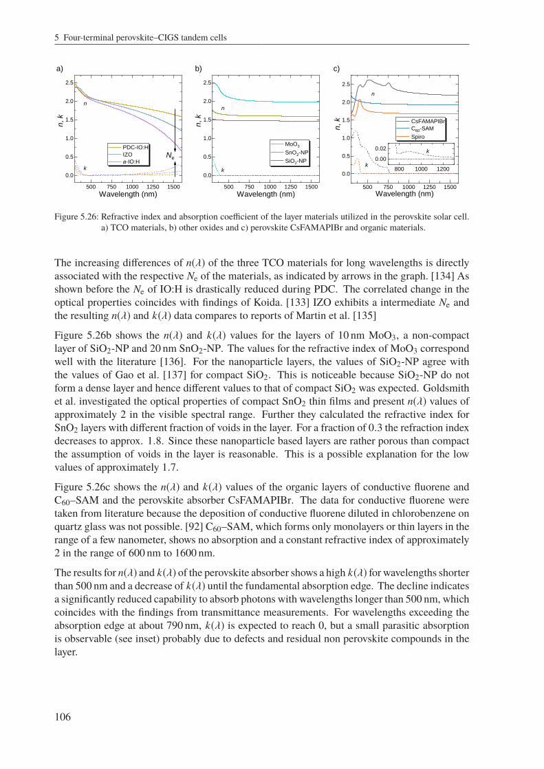
5 Four-terminal perovskite–CIGS tandem cells
500 750 1000 1250 1500
0.0
0.5
1.0
1.5
2.0
2.5
k
k
n,
k
Wavelength (nm)
n
CsFAMAPIBr
C60-SAM
Spiro
800 1000 1200
0.00
0.02
500 750 1000 1250 1500
0.0
0.5
1.0
1.5
2.0
2.5
MoO3
SnO2-NP
SiO2-NP
n,
kWavelength (nm)
n
k
500 750 1000 1250 1500
0.0
0.5
1.0
1.5
2.0
2.5
PDC-IO:H
IZO
a-IO:H
n,
k
Wavelength (nm)
n
k
Ne
a) b) c)
Figure 5.26: Refractive index and absorption coefficient of the layer materials utilized in the perovskite solar cell.a) TCO materials, b) other oxides and c) perovskite CsFAMAPIBr and organic materials.
The increasing differences of n(λ) of the three TCO materials for long wavelengths is directlyassociated with the respective Ne of the materials, as indicated by arrows in the graph. [134] Asshown before the Ne of IO:H is drastically reduced during PDC. The correlated change in theoptical properties coincides with findings of Koida. [133] IZO exhibits a intermediate Ne andthe resulting n(λ) and k(λ) data compares to reports of Martin et al. [135]
Figure 5.26b shows the n(λ) and k(λ) values for the layers of 10 nm MoO3, a non-compactlayer of SiO2-NP and 20 nm SnO2-NP. The values for the refractive index of MoO3 correspondwell with the literature [136]. For the nanoparticle layers, the values of SiO2-NP agree withthe values of Gao et al. [137] for compact SiO2. This is noticeable because SiO2-NP do notform a dense layer and hence different values to that of compact SiO2 was expected. Goldsmithet al. investigated the optical properties of compact SnO2 thin films and present n(λ) values ofapproximately 2 in the visible spectral range. Further they calculated the refractive index forSnO2 layers with different fraction of voids in the layer. For a fraction of 0.3 the refraction indexdecreases to approx. 1.8. Since these nanoparticle based layers are rather porous than compactthe assumption of voids in the layer is reasonable. This is a possible explanation for the lowvalues of approximately 1.7.
Figure 5.26c shows the n(λ) and k(λ) values of the organic layers of conductive fluorene andC60–SAM and the perovskite absorber CsFAMAPIBr. The data for conductive fluorene weretaken from literature because the deposition of conductive fluorene diluted in chlorobenzene onquartz glass was not possible. [92] C60–SAM, which forms only monolayers or thin layers in therange of a few nanometer, shows no absorption and a constant refractive index of approximately2 in the range of 600 nm to 1600 nm.
The results for n(λ) and k(λ) of the perovskite absorber shows a high k(λ) for wavelengths shorterthan 500 nm and a decrease of k(λ) until the fundamental absorption edge. The decline indicatesa significantly reduced capability to absorb photons with wavelengths longer than 500 nm, whichcoincides with the findings from transmittance measurements. For wavelengths exceeding theabsorption edge at about 790 nm, k(λ) is expected to reach 0, but a small parasitic absorptionis observable (see inset) probably due to defects and residual non perovskite compounds in thelayer.
106

5.4 Potential for further optimizations of perovskite–CIGS tandem solar cells
With the knowledge of n(λ) and k(λ) of each individual material of the PSC architecture, it ispossible to create a multi layer model in order to simulate the optical transmittance, reflectanceand absorptance of a real PSC device, as demonstrated by Tim Helder. [110] Here, the n(λ)and k(λ) data will be used in the next Section 5.4.1 for the modelling of complete 4T tandemarchitectures as part of a current loss analysis.
Current loss analysis by transfer matrix method
This section contains simulation results that are original work of the author and have beenpublished in [143].
In order to estimate the parasitic absorptance of each sublayer of a tandem cell, a simulationmodel is created comprising all layers with their optical parameters n(λ), k(λ) from the lastsection. The remaining optical data was taken from literature (ITO, [91] Spiro-OMeTAD, [92]air, [93] CIGS, [94] MoSe, [95] and molybdenum, MgF2, CdS, and i-ZnO. [96]). Two cell sizematched tandem devices from Section 5.3.2 with the setups PSCa+CIGSa and PSCb+CIGSb arechosen as the physical data basis of the simulation, aiming for a deeper understanding of theparasitic absorption in the different front electrodes of the PSCs, namely PDC–IO:H and ITO.
Via transfer-matrix-method, the absorptance losses in each layer were simulated and calculatedin terms of equivalent current densities using the program e-ARC. [90] The spectral dependencyof Ai of each layer i is cumulatively plotted in the colour coded graphs of Figure 5.27a andc following the relation 1 =
∑(Ai) + R. Additionally, the measured (symbols) and simulated
(lines) EQE responses are shown. Figure 5.27b and d depict schematic illustrations of the layerarchitectures and the results of the current loss analysis for the integration range up to 1165 nm.The simulation allows for the evaluation of the total JRef, the individual JAbs in each layer, thecurrent density equivalent of the recombination loss (JRec) and the JSim in the top and bottomcell.
To account for the shadow losses in the bottom cell introduced by the grid of the PSC top cell, theEQE and Ai are corrected for the shaded area of 2.7 % (see Section 5.1.2), assuming a negligibleamount of reflection and full absorption at the grid. An additional correction is made for thegrid of the CIGS cell, which is smaller and therefore shades only an area of 0.23 %.
107

5 Four-terminal perovskite–CIGS tandem cells
300 400 500 600 700 800 900 1000 1100 1200
0.0
0.2
0.4
0.6
0.8
1.0
EQE measuredPSCb CIGSa Tandem
EQ
E,
S(A
i)+
R
wavelength (nm)
EQE simulated PSCb CIGSa Tandem
300 400 500 600 700 800 900 1000 1100 1200
0.0
0.2
0.4
0.6
0.8
1.0
EQE measuredPSCa CIGSa Tandem
EQ
E,
S(A
i)+
R
wavelength (nm)
EQE simulated PSCa CIGSa Tandem
Tandem Cell
Area = 0.5 cm²
PCE = 20.5 %
Tandem Cell
Area = 0.5 cm²
PCE = 23.0 %
a)
R
PSCa NIR optimized
Perovskite Top Cell
Area = 0.5 cm²
FF = 67.6 %
VOC = 1183 mV
JSC = 18.6 mA cm-2
JEQE = 18.8 mA cm-2
JSim = 18.6 mA cm-2
PCE = 15.0 %
CIGSa Bottom Cell
Area = 0.5 cm²
FF = 78.0 %
VOC = 670 mV
JSC = 15.4 mA cm-2
JEQE = 15.3 mA cm-2
JSim = 14.9 mA cm-2
PCE = 8.0 % (solo 22.1%)
-5.47 -12.1%JRef
+33.50 +74.4%JSim
-5.56 -12.4%JAbs
0.11
AZO
CIGSb
Mo
Front glass
PSCa
IZO
PDC-IO:H+ 1.03
0.82
1.55
0.47
1.02
18.6
(mA cm-2)
-0.44 -1.0%JRec
45.0 100%AM1.5G (λ ≤ 1165 nm) qNph
14.9
b)
c) d)
Front Glass
Front Glass
R- 5.15 - 11.4%JRef
+ 32.23 + 71.6%JSim
- 7.14 - 15.9%JAbs
0.11
AZO
CIGSa
Mo
Front glass
PSCb
IZO
ITO 3.20
0.71
1.42
0.41
0.79
18.6
(mA cm-2)
- 0.47 - 1.0%JRec
45.0 100%AM1.5G (λ ≤ 1165 nm) qNph
13.6
0.46
0.04
0.41
0.03
0.04
0.03
0.03
0.03
PSCb Reference
Perovskite Top Cell
Area = 0.5 cm²
FF = 62.3 %
VOC = 1173 mV
JSC = 18.4 mA cm-2
JEQE = 19.0 mA cm-2
JSim = 18.6 mA cm-2
PCE = 13.7 %
CIGSa Bottom Cell
Area = 0.5 cm²
FF = 78.0 %
VOC = 663 mV
JSC = 13.2 mA cm-2
JEQE = 13.3 mA cm-2
JSim = 13.6 mA cm-2
PCE = 6.8 % (solo 15.6%)
R
R
Figure 5.27: Spectral evaluation of the EQE (measured and simulated), R (measured) and A (simulated) with corre-sponding current loss analyses and schematic illustrations of the tandem cell architectures PSCa+CIGSa(Figures a and b) and PSCb+CIGSa (c and d). The main difference between both tandem setups isthat PSCa is NIR optimized by comprising PDC–IO:H as a front electrode, while the reference PSCbuses ITO. The simulated absorptance spectra of each sublayer Ai are plotted cumulatively following∑(Ai) + R = 1 and colour coded correspondingly to the layer materials as denoted in the schematic
layer stack. The solo PCE of CIGSa is 22.1 % (compare tables 5.5 and 5.10).
Due to the superior transmittance of the PDC–IO:H and IZO (b), the losses in the top cellelectrodes are confined to only 1.0 mA cm−2 and 0.8 mA cm−2, respectively. In comparison tothe reference setup (d) comprising the unfavourable ITO (3.2 mA cm−2), the loss in the ZAOfront electrode is reduced by over 2 mA cm−2. In the bottom cell, the ZAO electrode of the CIGScell introduces losses of 0.4 mA cm−2 to 0.5 mA cm−2. In the reference setup, the sum of TCOrelated current losses is 4.3 mA cm−2, which is over 60 % of the total JAbs. In the NIR optimizedsetup the TCO losses are reduced to 40 %, which is still a significant fraction and demonstratesthe impact of the electrodes on the optical properties of the solar cell.
Additional losses are contributed to recombination and parasitic absorption in the perovskiteitself, while the interlayers in the tandem cell have a negligible contribution. Within theabsorption range of the bottom cell up to 1165 nm, a part of the NIR spectrum is also lost(0.8 mA cm−2 to 1.0 mA cm−2) to absorption at the molybdenum rear contact, due to insufficientNIR absorption in the CIGS and a low reflectivity of the molybdenum rear interface. The overallabsorption losses accumulate to 12.4 % for the NIR-optimized tandem cell and 15.9 % for thereference setup relative to the incident photon flux of the AM1.5.
108
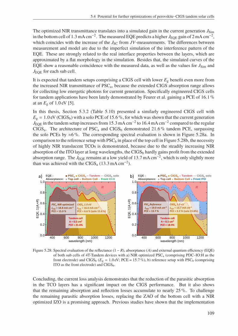
5.4 Potential for further optimizations of perovskite–CIGS tandem solar cells
The optimized NIR transmittance translates into a simulated gain in the current generation JSimin the bottom cell of 1.3 mA cm−2. Themeasured EQE predicts a higher JEQE gain of 2 mA cm−2,which coincides with the increase of the JSC from JV-measurements. The differences betweenmeasurement and model are due to the imperfect simulation of the interference pattern of theEQE. These are strongly related to the real interface properties between the layers, which areapproximated by a flat morphology in the simulation. Besides that, the simulated curves of theEQE show a reasonable coincidence with the measured data, as well as the values for JSim andJEQE for each sub cell.
It is expected that tandem setups comprising a CIGS cell with lower Eg benefit even more fromthe increased NIR transmittance of PSCa, because the extended CIGS absorption range allowsfor collecting low energetic photons for current generation. Specifically engineered CIGS cellsfor tandem applications have been lately demonstrated by Feurer et al. gaining a PCE of 16.1 %at an Eg of 1.0 eV [5].
In this thesis, Section 5.3.2 (Table 5.10) presented a similarly engineered CIGS cell withEg = 1.0 eV (CIGSb) with a solo PCE of 15.6 %, for which was shown that the current generationJEQE in the tandem setup increases from 15.3 mA cm−2 to 16.4 mA cm−2 compared to the regularCIGSa. The architecture of PSCa and CIGSb demonstrated 21.6 % tandem PCE, surpassingthe solo PCEs by ≈6 %. The corresponding spectral evaluation is shown in Figure 5.28a. Incomparison to the reference setup with PSCb in place of the top cell in Figure 5.28b, the necessityof highly NIR translucent TCOs is demonstrated, because due to the steadily increasing NIRabsorption of the ITO layer at long wavelengths, the CIGSb hardly gains profit from the extendedabsorption range. The JEQE remains at a low yield of 13.7 mA cm−2, which is only slightly morethan was achieved with the CIGSa (13.3 mA cm−2).
400 600 800 1000 12000.0
0.2
0.4
0.6
0.8
1.0
EQ
E, S
(Ai+
R)
wavelength (nm)400 600 800 1000 1200
0.0
0.2
0.4
0.6
0.8
1.0
EQ
E, S
(Ai+
R)
wavelength (nm)
EQE : PSCb CIGSb – Tandem --- CIGSb solo
Absorptance: Top cell Bottom Cell Front ITO
Tandem cellA = 0.5 cm²PCE = 21.6%
Tandem cellA = 0.5 cm²PCE = 18.9%
a) b)
PSCa NIR optimizedJEQE = 18.8 mA cm-2
PCE = 15.0 %
PSCb ReferenceJEQE = 19.0 mA cm-2
PCE = 13.7 %
CIGSb 1.0 eVJEQE = 16.4 mA cm-2
PCE = 6.6 % (solo 15.6 %)
CIGSb 1.0 eVJEQE = 13.7 mA cm-2
PCE = 5.2 % (solo 15.6%)
EQE : PSCa CIGSb – Tandem --- CIGSb solo
Absorptance: Top cell Bottom Cell Front IO:H
R R
Figure 5.28: Spectral evaluation of the reflectance (1− R), absorptance (A) and external quantum efficiency (EQE)of both sub cells of 4T-Tandem devices with a) NIR optimized PSCa (comprising PDC–IO:H as thefront electrode) and CIGSb (Eg = 1.0 eV; PCE = 15.7 %), b) reference setup with PSCb (comprisingITO as the front electrode) and CIGSb.
Concluding, the current loss analysis demonstrates that the reduction of the parasitic absorptionin the TCO layers has a significant impact on the CIGS performance. But it also showsthat the remaining absorption and reflection losses accumulate to nearly 25 %. To challengethe remaining parasitic absorption losses, replacing the ZAO of the bottom cell with a NIRoptimized IZO is a promising approach. Previous studies have shown that the implementation
109

5 Four-terminal perovskite–CIGS tandem cells
of IZOmay also lead to an improved stability and comparable efficiency values of theCIGS. [138]Additionally, the front electrode of the bottom cell CIGS could be adapted to the lower currentdensity in the tandem application by decreasing the TCO thickness and grid bar dimensions,reducing parasitic absorption even further.
In order to diminish the reflection losses, familiar concepts of light management such as anti-reflective coatings (ARC), surface structuring or optical coupling materials may be applied. Thefollowing Section 5.4.2 introduces a simple approach using immersion oil to fill the air gap inbetween the top and bottom cell. By this, the Fresnel reflection at the rear electrode to thePSC device shall be minimized. Furthermore, the option of using a structured anti reflectionfoil (ARF) will be evaluated to realize a better light incoupling at the PSC surface. A greaterreduction of the overall reflection is expected from a simulation assisted engineering of theindividual layer thicknesses, which could reduce the amount of disadvantageous interferencereflection patterns. On the one hand, the freedom of thickness variations is strongly limited bythe prerequisite to maintain full electrical functionality of the solar cell architecture, but on theother hand, the perovskite technology has proven to serve a great variety of different materialsand layer stack options, so that the development of an optically and electrically enhanced deviceis feasible in the future. Further development of the proposed optical models could be of valuableassistance to fulfil this tasks.
In general, this study utilized only perovskite with an Eg of about 1.6 eV, because the materialcomposition of choice provided the best efficiency and reproducibility. Lately, our collaboratorsat KIT showed that the band gap of the perovskite top cell can be increased, while maintainingvery high efficiencies. [3] Naturally, a higher band gap in the top cell enhance the bottom cellefficiency, and thus the tandem efficiency. The optimum band gap composition is still underdiscussion in experiment and simulation. [9,32,56] In this thesis, a fine-tuning of the band gap inconnection with an additional adjustment of the transmission will be evaluated on a simulationapproach later on in Section 5.4.3 to estimate the maximum achievable PCE values for thebottom cells CIGSa and CIGSb.
5.4.2 Improvement of the light management by using immersion oil for opticalcoupling and anti-reflective foil
In the so far tested 4T tandem cells, the top cell was mechanically stacked on top of the bottomcell, leaving an air gap in between. When the gap is simply left filled with air, the mismatchbetween the refractive indices of air and the electrode materials is causing unwanted Fresnelreflection losses. Equally, the glass surface of the superstrate of the top cell is in contact withair and causes reflection losses. This section evaluates the possibility to reduce the reflectionlosses by using immersion oil as an optical coupling material to replace the air in the gap in thetandem setup. Additionally, an anti reflection foil (ARF) with a pyramidal structure is used toenhance the light incoupling at the surface. The ARF has been kindly provided by collaboratorsfrom IMEC, who utilized a similar foil in perovskite–silicon tandem solar modules for optimallight harvesting. [12, 139]
At first for comparison, Figure 5.29 shows the basic effect of a regular ARC on a CIGS solarcell. The layer thickness is chosen such that the main reflection losses for wavelength between500 nm and 900 nm are diminished by the constructive interference effects (green area). Sincethe single layer ARC approach can be optimized only for certain wavelengths, this scenario
110
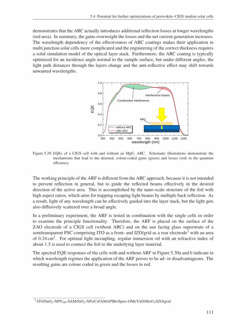
5.4 Potential for further optimizations of perovskite–CIGS tandem solar cells
demonstrates that the ARC actually introduces additional reflection losses at longer wavelengths(red area). In summary, the gains overweight the losses and the net current generation increases.The wavelength dependency of the effectiveness of ARC coatings makes their application inmulti junction solar cells more complicated and the engineering of the correct thickness requiresa solid simulation model of the optical layer stack. Furthermore, the ARC coating is typicallyoptimized for an incidence angle normal to the sample surface, but under different angles, thelight path distances through the layers change and the anti-reflective effect may shift towardsunwanted wavelengths.
300 400 500 600 700 800 900 1000 1100 12000.0
0.2
0.4
0.6
0.8
1.0
without ARC
with ARC
EQ
E
wavelength (nm)
Constructive interference
ARC
Interference losses
Figure 5.29: EQEs of a CIGS cell with and without an MgF2 ARC. Schematic illustrations demonstrate themechanisms that lead to the denoted, colour-coded gains (green) and losses (red) in the quantumefficiency.
The working principle of the ARF is different from the ARC approach, because it is not intendedto prevent reflection in general, but to guide the reflected beams effectively in the desireddirection of the active area. This is accomplished by the nano-scale structure of the foil withhigh aspect ratios, which aims for trapping escaping light beams by multiple back reflection. Asa result, light of any wavelength can be effectively guided into the layer stack, but the light getsalso diffusively scattered over a broad angle.
In a preliminary experiment, the ARF is tested in combination with the single cells in orderto examine the principle functionality. Therefore, the ARF is placed on the surface of theZAO electrode of a CIGS cell (without ARC) and on the sun facing glass superstrate of asemitransparent PSC comprising ITO as a front- and IZO/grid as a rear electrode3 with an areaof 0.24 cm2. For optimal light incoupling, regular immersion oil with an refractive index ofabout 1.5 is used to connect the foil to the underlying layer material.
The spectral EQE responses of the cells with and without ARF in Figure 5.30a and b indicate inwhich wavelength regimes the application of the ARF proves to be ad- or disadvantageous. Theresulting gains are colour coded in green and the losses in red.
3 ITO/SnO2-NP/C60-SAM/SiO2-NPs/CsFAMAPIBr/Spiro-OMeTAD/MoO3/IZO/grid
111

5 Four-terminal perovskite–CIGS tandem cells
300 400 500 600 700 800 900 1000 1100 12000.0
0.2
0.4
0.6
0.8
1.0
(i) CIGS
(ii) CIGS + Oil + Foil
EQ
E
wavelength (nm)300 400 500 600 700 800
0.0
0.2
0.4
0.6
0.8
1.0
(iii) Perovskite
(iv) Perovskite + Oil + Foil
EQ
E
wavelength (nm)
a) b)
Light trapping
Absorption in foil
Light outcoupling
in glass
Light trapping
(ii)(iv)
Optical foil
Oil
Optical foil
Oil
Figure 5.30: EQEs of a) a CIGS cell without ARC and b) a PSC with and without an anti-reflective foil that isplaced on top of the solar cell using immersion oil for optimal light in-coupling. Schematic illustrationsdemonstrate the mechanisms that lead to the denoted, colour-coded gains (green) and losses (red) inthe quantum efficiency.
In case of CIGS themain reflection losses without ARF (i) in the regime from 500 nm to 1000 nmcan be effectively suppressed with the ARF (ii). Due to multiple scattering at the pyramidalstructure, photons are effectively guided towards the solar cell or redirected towards it, if backreflected from the cells surface. This mechanism is called light trapping, as it is denoted in thegraph of Figure 5.30a.
Similarly in Figure 5.30b, the same mechanism applies for the PSC with ARF (iv), but herea counteracting mechanism limits the beneficial gains of the light trapping. Due to the muchlonger travelling distance through the ≈1 mm thick superstrate, the omnidirectional scatteredand back reflected photons are likely to be guided away from the active area and therefore lostfor current generation, as it is demonstrated in the schematic drawing. This effect is named lightoutcoupling. As a result, the competing mechanisms cancel each other out in average, bringingno significant advantage to the PSC EQE. Furthermore, the ARF itself has an absorption edgeat ≈320 nm, which reduces the EQE of the solar cell in that regime.
It should be noted here that the effect of light outcoupling is partly caused by the measurementsetup, where a collimated narrow beam of ≈1 mm in diameter is used to illuminate a fractionof the PSC active area. Since the active area itself has only a width of 3.75 mm, the amount ofoutcoupling losses is certainly increased by the low scattering angles that are needed for lightbeams to escape the active area. With full size illumination, e.g. under the solar simulator, acontrary effect is observed. Then, scattered light beams from outside of the Aact are guidedtowards it, increasing the current generation through light incoupling.
In tandem setups comprising the PSC as top cell, the CIGS as bottom cell, immersion oil isexpected to improve the light management, if used to fill the air gap and hence reducing themismatch of the refractive indices along the layer interfaces from top to bottom cell. In order toinvestigate this, Figure 5.31a shows the EQE response of the CIGS cell in the different tandemsetups with a representative PSC filter on top. The possible configurations with air (v), oil (vi)and additionally with ARF (vii) are schematically displayed in Figure 5.31b.
112
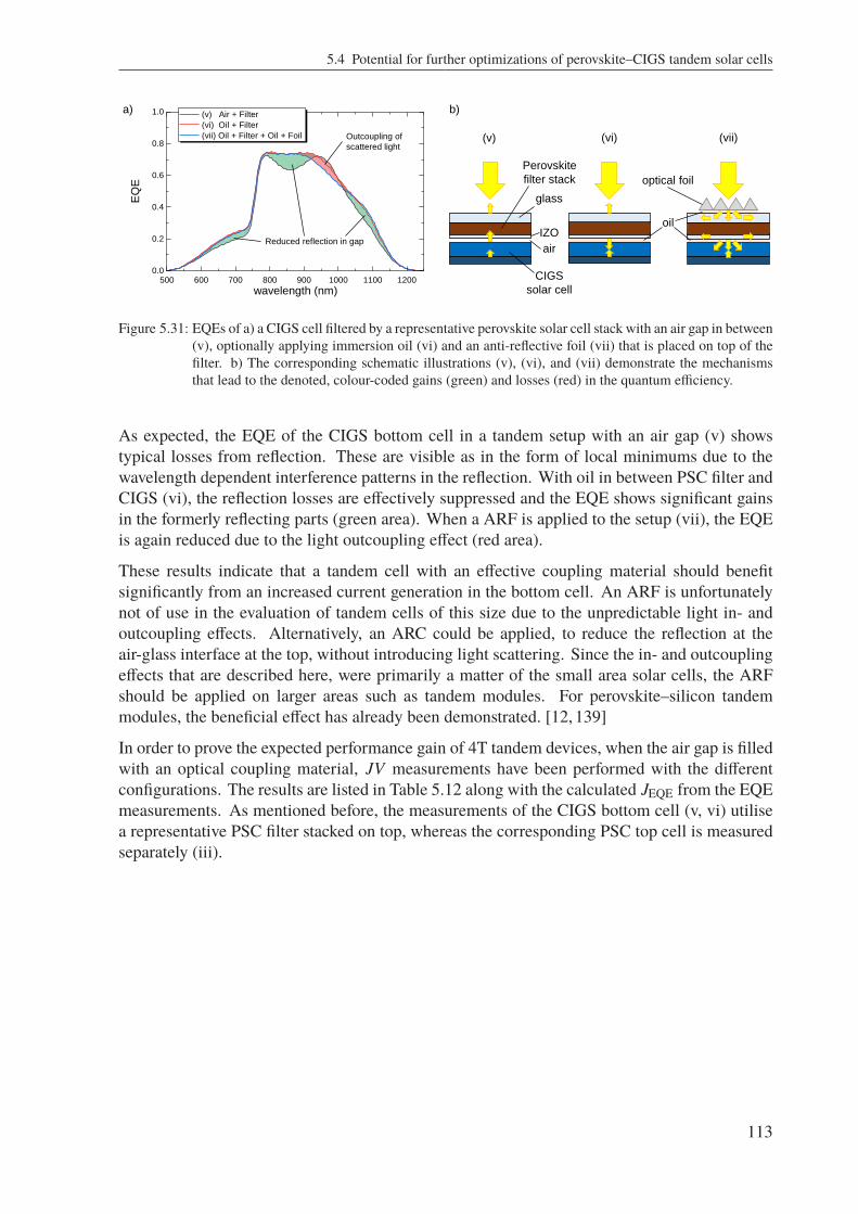
5.4 Potential for further optimizations of perovskite–CIGS tandem solar cells
500 600 700 800 900 1000 1100 12000.0
0.2
0.4
0.6
0.8
1.0 (v) Air + Filter
(vi) Oil + Filter
(vii) Oil + Filter + Oil + Foil E
QE
wavelength (nm)
a) b)
Reduced reflection in gap
Outcoupling of
scattered light(v) (vi) (vii)
glass
IZO
air
oil
optical foil
CIGS
solar cell
Perovskite
filter stack
Figure 5.31: EQEs of a) a CIGS cell filtered by a representative perovskite solar cell stack with an air gap in between(v), optionally applying immersion oil (vi) and an anti-reflective foil (vii) that is placed on top of thefilter. b) The corresponding schematic illustrations (v), (vi), and (vii) demonstrate the mechanismsthat lead to the denoted, colour-coded gains (green) and losses (red) in the quantum efficiency.
As expected, the EQE of the CIGS bottom cell in a tandem setup with an air gap (v) showstypical losses from reflection. These are visible as in the form of local minimums due to thewavelength dependent interference patterns in the reflection. With oil in between PSC filter andCIGS (vi), the reflection losses are effectively suppressed and the EQE shows significant gainsin the formerly reflecting parts (green area). When a ARF is applied to the setup (vii), the EQEis again reduced due to the light outcoupling effect (red area).
These results indicate that a tandem cell with an effective coupling material should benefitsignificantly from an increased current generation in the bottom cell. An ARF is unfortunatelynot of use in the evaluation of tandem cells of this size due to the unpredictable light in- andoutcoupling effects. Alternatively, an ARC could be applied, to reduce the reflection at theair-glass interface at the top, without introducing light scattering. Since the in- and outcouplingeffects that are described here, were primarily a matter of the small area solar cells, the ARFshould be applied on larger areas such as tandem modules. For perovskite–silicon tandemmodules, the beneficial effect has already been demonstrated. [12, 139]
In order to prove the expected performance gain of 4T tandem devices, when the air gap is filledwith an optical coupling material, JV measurements have been performed with the differentconfigurations. The results are listed in Table 5.12 along with the calculated JEQE from the EQEmeasurements. As mentioned before, the measurements of the CIGS bottom cell (v, vi) utilisea representative PSC filter stacked on top, whereas the corresponding PSC top cell is measuredseparately (iii).
113

5 Four-terminal perovskite–CIGS tandem cells
Sample JV data EQE data
ID Setup PCE FF VOC JSC JEQE(%) (%) (mV) (mA cm−2) (mA cm−2)
i CIGS 20.1 76.2 695 38.1 38.3iii PSC 15.8 71.6 1129 19.3 18.9
v Filter + Air + CIGS 7.1 77.5 659 13.8 13.8vi Filter + Oil + CIGS 7.6 76.4 661 14.9 15.1
iii + v PSC + Air + CIGS 22.9 4T-tandem efficiency estimations
iii + vi PSC + Oil + CIGS 23.4
Table 5.12: Solar cell parameters for a CIGS solar cell (i) and a semitransparent PSC (iii) as introduced in Figure5.30. Parameters for the CIGS, when a filter representing the PSC is stacked on top with air in between(v) and using immersion oil (vi) as shown in Figure 5.31. The JV data was obtained experimentallyfrom rvs JV scans and the JEQE from EQE measurements. For the estimation of PCE of the theoretical4T-tandem setups, the PCEf values of the filtered CIGS and the PSC were summarized according tothe notation.
According to the JV measurements, the CIGS bottom cell profits from the use of immersionoil by a PCEf increase from 7.1 % to 7.6 % and a JSC increase of 1.1 mA cm−2. The measuredJSC values match closely to the calculated JEQE values, proving the effective reduction of thereflection losses. A theoretical tandem setup with the PSC (iii), which has a PCE of 15.8 %,would reach a combined tandem PCE of 23.4 %.
As already mentioned before, the PSC comprises ITO as the front electrode, which is generallyunfavourable due to its high NIR absorption. But the gain of efficiency in the bottom cell ofmore than 0.5 % absolute due to the immersion oil should be directly transferable to other setupswith different electrode setups.
Unfortunately, the application of the oil is not easily accomplished when using actual solarcells instead of filters, because of several reasons. Firstly, the capillary forces strongly suckthe top cell towards the bottom cell, so that the release of both cells after measurement likelydamages the sensitive perovskite layers. Furthermore, for contacting the rear electrode of thePSC on the underside requires an electrical interconnection that the plane positioning on top ofthe bottom cell is difficult to accomplish without further technical arrangements. Lastly, oil thatspills besides the TCO electrode of the PSC is likely to penetrate the sensitive organic layers anddamage the cell. A filter is fully covered by the TCO, which is quite resistive to the oil and canbe rinsed with alcohol afterwards.
For future development steps, the positive results of the immersion oil imply that an alternativecoupling material could be applied to connect top and bottom cell such as a thermoplasticpolymer, in order to serve a permanent encapsulation and a beneficial optical coupling. Asuitable candidate could be poly(methyl methacrylate) (PMMA) since it has a similar refractiveindex of about 1.5 compared to immersion oil.
114

5.4 Potential for further optimizations of perovskite–CIGS tandem solar cells
5.4.3 Increasing the CIGS efficiency by implementing wide band gap top cellswith higher transmission
This section contains experimental transmittance data of filter stacks and PCE data of semi-transparent PSCs prepared by Saba Garibzadeh and Ihteaz M. Hossain from KIT. Detailedinformation is published in [3]. The following spectral analysis and simulation is original workof this thesis.
For the highest theoretical tandem PCE the Eg of the PSC should be increased to an optimumvalue of ≈1.7 eV, while keeping the PSC performance on a high level. Here, the impact of PSCswith a series of wider band gaps on the performance of the CIGS cells and hence the tandemPCE is evaluated with samples provided by collaboration partners from KIT.
Due to the increase of the Eg, the fundamental absorption edge shifts to lower wavelengths asit is observable in the T curves in Figure 5.32a for a set of different PSC filters from KIT. Thetransmittance after the fundamental absorption edge (T f ) is generally lower compared to thein-house prepared PSC (dashed line) due to a different electrode setup based on ITO instead ofIO:H and IZO. The architecture of the KIT PSC filters is described in reference [3].
The shift of the absorption edge from 1.63 eV to 1.83 eV leads to a significant increase of theJTrn of more than 4 mA cm−2 in the integration limit wavelength up to 1200 nm, as shown inFigure 5.32b. As expected, the higher T f of the ZSW PSC (Eg= 1.62 eV) leads also to a gainof ≈2 mA.cm−2 in JTrn if compared to the KIT sample with a similar Eg. However, the spectralresponse of the bottom cell is certainly higher for shorter wavelengths, so that the strongestimpact on the CIGS PCEf is expected from the PSCs with a wider band gap.
Figure 5.32c shows the estimated tandem PCEs, using the single diode model approach forsimulating the bottom cell power conversion efficiency obtained from single diode model sim-ulation (PCESim) of the CIGS cell with Eg = 1.1 eV (CIGSa) and using the PCEs of PSCs thatare equivalent to the filter architectures which are measured at the KIT.
500 600 700 800 900 1000 1100 12000
20
40
60
80
100
Eg (eV)
1.62 ZSW
1.63 KIT
1.68
1.73
1.78
1.83
T (
%)
Wavelength (nm)
Eg
500 600 700 800 900 1000 1100 12000
2
4
6
8
10
12
14
16
18
20
22
Eg (eV)
1.62 ZSW
1.63 KIT
1.68
1.73
1.78
1.83
Inte
gra
ted J
Trn
(m
A c
m-2
)
Wavelength (nm)
Eg
1.63
1.68
1.73
1.781.83
1.62
12 13 14 15 16 17 18
7.5
8.0
8.5
9.0
9.5
25.5
26.0
26.5
27.0
27.5
26
27
21
22
23
24
25
Estim
ate
d T
andem
PC
E (
%)
Sim
ula
ted C
IGS
a P
CE
(%
)
PSC PCE (%)
Eg
PSC from
KIT
ZSW
a) b) c)
Figure 5.32: a) Spectral T of PSC filters from Zentrum für Sonnenenergie- und Wasserstoff-Forschung Baden-Württemberg (ZSW) and KIT with different Eg in the range of 1.62 eV to 1.83 eV; b) Integral curvesof JTrn of the same filters; c) Estimated PCEs of principle tandem setups of CIGSa as a bottom celland the PSCs with different band gaps as top cells. Here, the PCE of the CIGSa is simulated by thesingle diode model, using the T of the PSC filters as an input. The PCE of the PSCs is obtained fromMPP tracking of equivalent PSCs devices from KIT and ZSW.
115

5 Four-terminal perovskite–CIGS tandem cells
As expected, the increase of the Eg is followed by a strong performance gain in the bottom cell.Filtered by the PSC filter with the lowest Eg of 1.63 eV, the CIGSa reaches only about 7.7 %,while the maximum bottom cell PCESim of 9.6 % is reached at 1.83 eV. However, the besttandem performance with an estimated PCE of 25.2 % is met with the PSC with 1.63 eV, whichhas a much higher reported PCE of 17.5 %. With the increase of the Eg, the PSCs themselveslose in PCE, which is not fully compensated by the PCE gains in the bottom cell. As a result,the three PSCs with the lower Eg values of 1.63 eV, 1.68 eV and 1.73 eV achieve quite similartandem PCEs over 25 %, while the wider band gap setups lose tandem performance.
Comparing the tandem setups with the 1.62 eV (ZSW) and 1.63 eV (KIT) samples, a differencein the CIGS PCESim of an absolute value of ≈0.5 % is observed that is reasoned the superiortransmittance of the ZSW sample. Of course the tandem performance with the ZSW PSC islower, because of the lower perovskite performance, but it raises the question, what would be themaximum bottom cell performance, if the T f would be higher for the PSCs with different Eg.
In order to estimate the bottom cell PCE for any setup with a fictional higher T f , a set of PSCfilter models has been generated that mimic the T of the real filters near Eg, but the T f is set tofix values of 70 % to 95 %. The spectral T data of the set is shown in Figure 5.33a. Followingthe same single diode model simulation approach from Section 5.2, the PCE of CIGSa in allpossible combinations is mapped in Figure 5.33b. The PCEs are plotted versus the Eg using acolour coded heat map for denoting the T f . For comparison, also the experimental values aremarked. Figure 5.33b shows a similar colour map for CIGSb.
The positions of the experimental data points indicate that their actual T f responses correlateto a theoretical linear T f of around 75 %. Small deviations originate from the positions of theinterference maxima in the real T spectra.
a) b) c)
500 600 700 800 900 1000 1100 12000
20
40
60
80
100
959085807570
Tf (%)
T (
%)
Wavelength (nm)
Eg (eV)1.631.681.731.781.83
1.63 1.68 1.73 1.78 1.83
761 738 717 697 678
7
8
9
10
11
12
13
Tf (%)
70
75
80
85
90
95
Wavelength (nm)
CIG
Sa P
CE
(%
)
PSC Eg (eV)
100
Experimental data
KIT
ZSW
1.63 1.68 1.73 1.78 1.83
761 738 717 697 678
6
7
8
9
10
Wavelength (nm)
CIG
Sb P
CE
(%
)
PSC Eg (eV)
Tf (%)
70
75
80
85
90
95
100
Figure 5.33: a) Spectral T of PSC filter models with different Eg and a linear transmittance after the fundamentalabsorption edge (Tf ) up to 95 % as indicated; Simulated PCE of b) CIGSa and c) CIGSb versus Eg ofthe PSC filter models. The colour coded scale denote the corresponding Tf . Additional experimentaldata is shown in b).
116

5.4 Potential for further optimizations of perovskite–CIGS tandem solar cells
However, the simulation predicts that the bottom cell PCE could be increased by an absoluteof approximately 2 % for all setups, if the T f would be increased to 95 %. It also predicts thatthe maximum PCE that could be reached with the CIGS cell with Eg = 1.1 eV (CIGSa) inapplication, is limited to ≈10 % when using a top cell with a narrow Eg and ≈12 % with a widerEg. The CIGS cell with Eg = 1.0 eV (CIGSb) would reach maximum PCEs between 8 % and10 %, respectively.
In an estimation example, CIGSa would have a PCESim of about 9.5 %, assuming perovskitesolar cell with a decent transmittance of 80 % and a band gap of 1.75 eV. This would lead toa tandem efficiency of 28 % or more, only if the PSC is highly efficient with a PCE of over18.5 %. Increasing the transmittance to 90 % would boost the bottom cell PCEf to 10.5 % andthe tandem to 29 %, respectively.
For tandem PCEs to approach 30 % in the future, two consequences are conceived from theseresults: (i) The bottom cell must become more efficient in the collection and conversion ofphotons with long wavelengths and (ii) The top cell must increase the transmittance and theoverall photovoltaic performance.
Both issues demand for a profound knowledge on the loss mechanisms, where incident photonsare not converted to current but reflected, scattered, or parasitically absorbed. The proposedoptical models in Section 5.4.1 may serve this task in the future.
117


6 Summary
This thesis focuses on the development of efficient perovskite–CIGS tandem solar cells withan enhanced spectral response in the near-infrared spectrum. In the process, perovskite solarcells (PSCs) were fabricated with high power conversion efficiency and high transparency.To increase their transmission in the near-infrared (NIR) spectrum, hydrogen-doped indiumoxide (IO:H) and indium zinc oxide (IZO) films were investigated and implemented as front andrear electrodes for the PSC. Cell-size-matched four-terminal (4T) tandem solar cells with anactive area of 0.5 cm2 were developed that reach a power conversion efficiency (PCE) of 23.0 %.
In the first part of this thesis, fundamental challenges regarding the solution-based fabrication ofPSCwere identified and overcome by sophisticated interface engineering. A large issue is causedby ion accumulation at the electron transport layer (ETL) interface with the perovskite, whichhinders charge extraction and results in a pronounced hysteresis with an irregular response of thephotocurrent during a voltage scan depending on the sweep direction. Passivating the interfacewith a C60-based self-assembled monolayer (C60–SAM) effectively suppressed the hysteresis,but the highly non-polar molecules introduced severe wetting issues during the subsequentdeposition of the perovskite precursor.
To increase the low surface energy of the organic fullerene layer, a wetting agent was developedon the basis of insulating oxides nanoparticles such as SiO2 and Al2O3 with diameters between20 nm to 60 nm. Contact angle measurements revealed that the insulating nanoparticles causea strong increase of the surface energy already when covering only fractions of 10 % to 15 %of the interface. The wetting agent thus facilitated the perovskite formation to the extent that ahomogeneous layer was feasible even on larger areas.
On the pathway to semitransparent PSCs, highly NIR transparent and yet conductive IO:Hand IZO electrodes were developed. Sputter deposited and subsequently crystallized IO:H wasidentified as a suitable front electrode on the glass superstrate with the best optical properties,using H2 gas as the doping source during deposition. This approach achieved state-of-the-artconductive properties with a high charge carrier mobility (µ) of over 90 cm2 V−1s−1 and a lowelectron density (Ne) of under 2 × 1020 cm−3 at an ultra-low NIR absorptance below 2 %.
For the rear electrode deposition on the sensitive organic hole transport layer (HTL), amorphousIZO in combination with a MoO3 protective layer proved to be the best choice in terms ofavoiding sputter damage, low absorption and low resistivity. The perovskite absorber followed amixed cation approach with a band gap of ≈1.6 eV, fixing the absorption edge at about 780 nm.From a thorough investigation of the spectral properties of the semitransparent PSCs, it canbe concluded that IO:H and IZO outperform traditional transparent conductive oxides (TCOs)such as indium tin oxide (ITO) or fluorine doped tin oxide (FTO), lowering the integral NIRabsorptance from over 20 % to below 7 % while maintaining a high photovoltaic PCE of over15 %.
119
6 Summary
Variations of the TCO layer thickness unveiled the complex balancing between optical propertiesand electrical performance for the given solar cell geometry. As expected, thinner rear electrodeslead to a lower parasitic absorption accompanied by higher series resistance, but it was also foundthat the transmittance suffers from high internal reflection interference. Hence, intermediatelayer thicknesses proved to have the advantage of a better transmission and an improved electricalperformance.
The second part of this thesis concentrated on combining the semitransparent PSCs with copperindium gallium diselenide (CIGS) solar cells into tandem setups. Because the race to publishperovskite record values has led to announcements of tandem device efficiencies derived fromvaguely filtered bottom cells and tiny top cells, one goal of this thesis was to evaluate thediscrepancy between a real cell-size-matched tandem device and a filtered cell stack estimation.A simple study of the transmittance of diverse semitransparent PSC and their sister filtersquickly confirmed a spectral disparity. Especially with the use of in-house made electrodes,slight thickness variations lead to interference-induced mismatches of up to 3.6 %.
However, the comparably small transmittance mismatch should not cause concern because thereal performance limiting factors hide behind the small area of the perovskite. Considering thepossible challenges of a homogeneous layer deposition in the solution-based processes, it is nocoincidence that the record PCE values are reported for tiny perovskite devices. Furthermore, theresistivity of the transparent electrodes becomes significantly more important upon increasingthe cell size. To realize an area of 0.5 cm2, one dimension of the cell will be at least 7 mm wide,which is already comparable to the width of a cell in a typical module made of interconnectedparallel cell stripes.
A metal grid is implemented to minimize the resistive losses in the TCO electrodes, loweringthe series resistance of the solar cell by over 60 % in case of 0.24 cm2 PSCs and by 30 % ona larger area of 0.5 cm2. Remarkably, and perhaps due to the beneficial effect of the wettingagent on the perovskite layer homogeneity, the best large area PSC reached a steady-state PCEof 15.0 %. Combined with a high-efficiency CIGS solar cell of the same area, the resulting 4Ttandem device demonstrated a champion PCE of 23 %.
Additional simulations with hypothetical filters to represent perovskite absorbers with a rangeof different band gaps showed that the required high efficiencies over 10 % for the CIGS bottomcell can only be reached when the band gap of the perovskite is increased to a minimum of≈1.75 eV and in combination with a high transmittance after its absorption edge (≈720 nm) ofabout 90 %.
In order to investigate the remaining loss mechanisms in the tandem setup, a sophisticatedcurrent loss analysis was performed. In the process, spectroscopic ellipsometry measurementswere conducted on the single layers of the PSC in order to determine their optical functionsn and k for inclusion in a simulation model of the whole 4T tandem architecture. The modelenables the parasitic absorption of each layer of the complete tandem stack to be addressed.
As a result, it shows that the main absorption losses are attributed to the TCOs while theinterlayers contribute only a minor fraction. Already the replacement of the ITO front electrodeof the PSC by an IO:H electrode avoids current density losses of over 2 mA cm−2. Hence, theoverall relative absorption related current loss is reduced from 16 % to 12 %, which is equalto the current losses introduced by reflection (12 %). Further significant losses are due toimperfections of the perovskite, shadowing by the metal grid and insufficient absorption of NIRphotons which are lost at the rear electrode of the CIGS bottom cell.
120
6 Summary
in conclusion, there is quite some potential to improve the performance of the tandem cell froman optical point of view. At first, the reflection losses must be minimized. A simple experimentwith immersion oil as an optical couplingmaterial in between the gap of a perovskite filter and theCIGS bottom cell demonstrated that the reflection losses at long wavelengths from the interfaceof the PSC rear electrode can be drastically reduced. These reflection losses are confirmed inthe current loss analysis, which indicates that a suitable filler material with a matched refractiveindex could be used to glue top and bottom cell together. On the one hand this would serve asencapsulation and on the other hand improve light management, leading to a win-win situation.
A different approach is needed for the front interface. Here, experiments with a textured anti-reflective foil showed that due to the thick glass superstrate in the front, no beneficial effectscould be achieved because if only a fraction is illuminated the light is scattered away fromthe active area. Illumination of a larger fraction leads to the opposite effect with more lightcoupling into the active area. Consequently, the texturing approach could lead to better lightmanagement, but only on large-area devices such as modules in which the scattered light wouldalways encounter the active area at some point. Additionally, a simple anti-reflective coatingon the glass side might not lead to the desired gain, because a large amount of reflection isintroduced internally at the interfaces. These act as reflective resonators for wavelengths thatmatch the interlayer distances. Hence, a sensitive fine-tuning of the interlayer thicknesses wouldlead to a more significant improvement of the transmissive properties of the top cell. The opticalmodels developed in this work, will contribute to this development in the future.
Regarding the remaining parasitic absorption in the TCO electrodes, a great further reductionhere is only possible under certain preconditions, because the main losses could be alreadyeffectively reduced by exchanging the front electrode ITO with post-deposition-crystallisedhydrogenated indium oxide (PDC–IO:H). As long as the reflection is still high and the perovskiteabsorber layer itself also contributes a significant amount of parasitic absorption (includingrecombination losses), not much light transmits to the underlying TCO layers. As a result theimplementation of even better TCOs in place of the rear electrode of the PSC or replacing theTCO of the CIGS would have only a small effect.
For future development steps, the tasks can be formulated from the above findings:
• Reduction of the reflection at the rear electrode of the PSC
• Simulation assisted adjustment of all layer thicknesses to reduce internal reflection
• Advanced perovskite absorbers with less parasitic absorption and optimal band gap
• Highly NIR optimized TCOs also for CIGS
• Improved CIGS efficiency in the NIR
There aremany other challenges of the new perovskite technologywhich have not been addressedin this thesis, such as degradation issues, thermal stability, lead elution, upscaling, solventtoxicity, and the like. The list is long, but because there is so much research and industrialeffort involved in this fascinating topic, perovskites seem to be ready to tackle all remainingchallenges. I therefore believe that perovskites have an excellent chance to succeed as a newplayer in the PV world. I am looking forward to a bright perovskite future, especially in tandemapplications and consequently with CIGS as a thin-film teammate.
121


A Appendix
A.1 Ellipsometry models
Drude model (D): A Drude model is used for the description of free carriers like they occur ina materials like metals or highly doped semiconductors (like TCOs). The dielectric functions isdefined as:
ε(ω) = ε1∞ −ω2
p
ω2 + iωτν(A.1)
with the frequency ω in units of 1/s and where ωp =√( Ne2
ε0m∗ ) is the resonance frequency whichrepresents the amplitude of the oscillator and ωτ =
eµm∗ the damping constant. From this
relations carrier concentration, mobility and effective mass can be determined. The value of thedielectric function in infinity ε1∞ is typically fixed at 1.
Tauc-Lorentz model (TL): This model is mainly used to describe transparent dielectric andamorphous materials with an absorption edge. It is based on the expression for ε2(E). ε2(E) isobtained from Kramers-Kronig relation.
ε2(E) =
AE0C(E−Eg)2
(E2−E20 )
2+C2E21E , E > Eg
0 E ≤ Eg(A.2)
ε1(E) = ε1∞ +2π
P∫ ∞
Eg
xε2(x)x2 − E2 dx (A.3)
In the TL model, the dielectric functions are obtained from the five parameters band gap Eg,the amplitude A, the resonance frequency E0 and the broadening of the oscillator C. The unitsof these parameters is eV. The given formula is for a single oscillator, but using multiple TLoscillators to describe a material may be reasonable.
Cody-Lorentz model (CL): The CL model is similar to the TL model but with an additionalUrbach term in order to simulate Urbach tail for the absorption of photons with energy smallerEg.
ε2(E) =
AE0CE(E−Eg)2
((E2−E20 )
2+C2E2)((E−Eg)2+E2p), E > Et
E1E exp
((E−Et)
EU
)E ≤ Et
(A.4)
ε1(E) = ε1∞ +2π
P∫ ∞
Eg
xε2(x)x2 − E2 dx (A.5)
Parameters A, E0,C and Eg are the same as in the TLmodel. Ep, Et, EU are additional parametersdue to the Urbach term.
123

A Appendix
Cauchy model (C): A Cauchy model is often used for transparent dielectric materials. TheCauchy relation uses the first two even orders of a polynomial description of n(λ) and k(λ):
n(λ) = n0 + C0n1
λ2 + C1n2
λ4 (A.6)
k(λ) = k0 + C0k1
λ2 + C1k2
λ4 (A.7)
with the wavelength λ in units of nm. The optical functions are obtained by fitting the sixparameters n0,n1,n2, k0, k1, k2. The coefficients C0 = 102 and C1 = 107 are fixed.
For the best description of the TCO materials of this study, a Drude model for the modellingof free carrier absorption is combined with another model for the interband transitions. For theinterband transition modelling, Tauc-Lorentz and Cody-Lorentz models are suitable and widelyused [73]. ADrudemodel in combination with a Tauc-Lorentzmodel was used for modelling theamorphous layers IZO and a-IO:H (both 180 nm). For PDC-IO:H layers (with a layer thicknessof 220 nm) with polycrystalline structure, a combination of Drude and Cody-Lorentz was used.
For the modeling of MoO3, a Tauc-Lorentz model was used to design both the band gap and theclose to zero absorption for wavelengths greater than 400 nm. The values for the refractive indexcorrespond well with the literature [136]. For the nanoparticle layers, Cauchy models were usedsince no absorption and no band to band transitions take place. The values of SiO2 –NP agreewith the values of Gao et al. [137] for compact SiO2. Goldsmith et al. calculated the refractiveindex of approx. 1.8 for SnO2 layers with a fraction of voids of 0.3, which is comparable to ourresults for the non-compact nanoparticle based layers. [140]
The data for Spiro-MeOTAD were taken from literature because the deposition on quartz glasswas not possible. [92] For the simulation of C60 –SAM a Tauc-Lorentz model was used. Forthe simulation of the perovskite absorber, 8 Tauc-Lorentz oscillators were used in one model.For wavelength higher than 800 nm k drops to values in the range of 0 but a small residualabsorption is observable (see inset).
The parameters of the optical models of the simulation are listed in Table A.1.
124

A.1 Ellipsometry models
Layer RMS d (nm) Model Parameters
a-IOH 3.06 156 TL Eg (eV) A (eV) E0 (eV) C (eV)2.9943 474660 2.7136 14.8437
D ωp (cm−1) ωτ (cm−1)12313.31 774.41
PDC-IO:H 5.58 210 CL Eg (eV) A (eV) E0 (eV) C (eV) Ep (eV) Et (eV) EU (eV)2.419 87.18 8.5978 19.1496 3.1469 4.0013 0.2507
D ωp (cm−1) ωτ (cm−1)7938.99 403.6
IZO 0.69 168 TL Eg (eV) A (eV) E0 (eV) C (eV)1 2.5389 18237 13.0974 2.18412 4.6027 201151 5.535 18.02863 2.6258 38788 4.2672 2.4085D ωp (cm−1) ωτ (cm−1)
10431.21 628.14
SiO2 –NP 0.42 25 C n0 n1 n2 k0 k1 k2
1073 39.5 25.4 0 -385 282
SnO2 –NP 0.31 12 C n0 n1 n2 k0 k1 k2
1223 120.6 30.2 10 -55535 50163
Perovskite 0.95 384 TL Eg (eV) A (eV) E0 (eV) C (eV)1 0.0121 32 1.4346 0.4772 1.5961 62222 1.6323 0.10193 1.5533 12133 2.0226 0.94814 1.5138 5800 2.5122 0.63665 2.0564 34779 2.6747 1.24766 2.7076 38236 3.0059 0.49397 2.8999 99772 3.1361 0.71498 4.1076 142975 4.6938 2.9157
C60 –SAM 0.44 2.6 TL Eg (eV) A (eV) E0 (eV) C (eV)3.939 410001 4.1034 13.5611
MoO3 0.39 10 TL Eg (eV) A (eV) E0 (eV) C (eV)3.0485 656802 1.7095 5.4024
Table A.1: Parameters used for the optical models for fitting the spectral ellipsometry data and for simulating theoptical functions n and k of each layer. The quality of the fit is evaluated by the root mean square errorRMS.
125

A Appendix
A.2 Quantum efficiency measurements
To evaluate the spectral properties of the PSC, we performed external quantum efficiency (EQE)and transmittance (T) measurements. In contrast to the JV measurements under illumination ofthe full cell area, the illuminated area during EQE and T measurments is restricted to 0.05 cm2
in order to fit between the grid bars (see Figure A.1). By this, all incident photons of the probebeam may be either absorbed, reflected or transmitted in the layers of the tandem cell, withoutinfluence of the grid. In order to make sure, that no significant error is introduced by illuminatingonly a fraction of the active area, leaving a big fraction of dark area, we discuss briefly differentpreconditions for appropriate measurements in the following.
Layer homogeneity: Figure A.2 shows that the EQE responses of 0.24 cm2 and 0.5 cm2 sizedcells are comparable, speaking for a equally good charge generation and collection in sampleswith different active areas. From the transmittance curves of the devices in the same graph, weobserve a significant shift of the T patterns, which indicates layer thickness differences betweenthe devices. This shows that – despite fabrication with equal process parameters – the exactreplication of the optical properties can not be guaranteed. In contrast, the optical properties ofa single device are very homogeneous, since no significant difference in EQE or T is observedby moving the measurement spot in different positions of each sample.
Shunts and dark area: Local shunts would deteriorate the EQE response, if they are close tothe measurement spot or close to the contact (grid). Without significant shunts, the EQE isquite independent from the resistive properties of the solar cell since it is measured under shortcircuit conditions (V = 0). Likewise, the dark area should be irrelevant to the measurement,because it is resembled by a parallel diode that locks under short circuit conditions with a highresistance. The absence of significant shunts is proven by the high parallel resistance of severalkΩ as obtained from JV measurements of the devices.
126

A.2 Quantum efficiency measurements
8.8 mm+
−b)
Front TCO StructuringContacts
Active area 0.5 cm2
Perovskite
a)
+ −
Rear
TCO
Front TCO StructuringContacts
Active area 0.24 cm2
Perovskite
Measurementspot 0.05 cm2 (EQE, T, R)
Measurementspot 0.05 cm2 (EQE, T, R)
Figure A.1: a) Photograph and scheme of a perovskite device with two solar cells of an active area of 0.24 cm2 andof b) 0.5 cm2. The yellow spot between the grid bars denotes the area (0.05 cm2), which is illuminatedduring EQE, T and R measurements of the single cells or tandem cells. During JV measurements, thefull active area is illuminated.
400 600 800 1000 12000
20
40
60
80
100
T
EQ
E,
T (
%)
Wavelength (nm)
0.24 cm2
0.5 cm2
EQE
Equivalent
filter stacks
0.24 cm2
0.5 cm2
Figure A.2: EQE and T measurements of PSC of the same architecture with different active area. Additionally,T spectra of filter stacks are shown which were prepared under nominally the same conditions andprocess parameters at different times.
127


Bibliography
[1] T. Todorov, O. Gunawan, and S. Guha, “A road towards 25% efficiency and beyond:Perovskite tandem solar cells,” Molecular Systems Design & Engineering, vol. 1, no. 4,pp. 370–376, 2016.
[2] H. Shen, T. Duong, J. Peng, D. Jacobs, N. Wu, J. Gong, Y. Wu, S. K. Karuturi,X. Fu, K. Weber, X. Xiao, T. P. White, and K. Catchpole, “Mechanically-stacked per-ovskite/CIGS tandem solar cells with efficiency of 23.9% and reduced oxygen sensitivity,”Energy & Environmental Science, vol. 11, pp. 394–406, Feb. 2018.
[3] S. Gharibzadeh, B. A. Nejand,M. Jakoby, T. Abzieher, D. Hauschild, S.Moghadamzadeh,J. A. Schwenzer, P. Brenner, R. Schmager, A. A. Haghighirad, L. Weinhardt, U. Lemmer,B. S. Richards, I. A. Howard, and U. W. Paetzold, “Record Open-Circuit Voltage Wide-Bandgap Perovskite Solar Cells Utilizing 2D/3D Perovskite Heterostructure,” AdvancedEnergy Materials, vol. 9, no. 21, p. 1803699, 2019.
[4] E. Avancini, R. Carron, B. Bissig, P. Reinhard, R. Menozzi, G. Sozzi, S. D. Napoli,T. Feurer, S. Nishiwaki, S. Buecheler, and A. N. Tiwari, “Impact of compositionalgrading and overall Cu deficiency on the near-infrared response in Cu(In, Ga)Se2 solarcells,” Progress in Photovoltaics: Research and Applications, vol. 25, no. 3, pp. 233–241,2017.
[5] T. Feurer, B. Bissig, T. P. Weiss, R. Carron, E. Avancini, J. Löckinger, S. Buecheler, andA. N. Tiwari, “Single-graded CIGS with narrow bandgap for tandem solar cells,” Scienceand Technology of Advanced Materials, vol. 19, no. 1, pp. 263–270, 2018.
[6] D. H. Kim, C. P. Muzzillo, J. Tong, A. F. Palmstrom, B. W. Larson, C. Choi, S. P. Harvey,S. Glynn, J. B. Whitaker, F. Zhang, Z. Li, H. Lu, M. F. van Hest, J. J. Berry, L. M.Mansfield, Y. Huang, Y. Yan, and K. Zhu, “Bimolecular additives improve wide-band-gap perovskites for efficient tandem solar cells with cigs,” Joule, vol. 3, no. 7, pp. 1734 –1745, 2019.
[7] Q. Han, Y.-T. Hsieh, L. Meng, J.-L. Wu, P. Sun, E.-P. Yao, S.-Y. Chang, S.-H. Bae,T. Kato, V. Bermudez, and Y. Yang, “High-performance perovskite/Cu(In,Ga)Se2 mono-lithic tandem solar cells,” Science, vol. 361, no. 6405, pp. 904–908, 2018.
[8] M. Jošt, T. Bertram, D. Koushik, J. A. Marquez, M. A. Verheijen, M. D. Heinemann,E. Köhnen, A. Al-Ashouri, S. Braunger, F. Lang, B. Rech, T. Unold, M. Creatore, I. Lauer-mann, C. A. Kaufmann, R. Schlatmann, and S. Albrecht, “21.6%-Efficient MonolithicPerovskite/Cu(In,Ga)Se2 Tandem Solar Cells with Thin Conformal Hole Transport Lay-ers for Integration on Rough Bottom Cell Surfaces,” ACS Energy Letters, pp. 583–590,2019.
[9] M. Langenhorst, B. Sautter, R. Schmager, J. Lehr, E. Ahlswede, M. Powalla, U. Lemmer,B. S. Richards, andU.W. Paetzold, “Energy yield of all thin-film perovskite/CIGS tandemsolar modules,” Progress in Photovoltaics: Research and Applications, vol. 27, no. 4,pp. 290–298, 2019.
129
Bibliography
[10] P. Mantilla-Perez, T. Feurer, J.-P. Correa-Baena, Q. Liu, S. Colodrero, J. Toudert, M. Sal-iba, S. Buecheler, A. Hagfeldt, and A. N. Tiwari, “Monolithic CIGS–Perovskite TandemCell for Optimal Light Harvesting without Current Matching,” ACS Photonics, vol. 4,no. 4, pp. 861–867, 2017.
[11] U. W. Paetzold, M. Jaysankar, R. Gehlhaar, E. Ahlswede, S. Paetel, W. Qiu, J. Bastos,L. Rakocevic, B. S. Richards, T. Aernouts, M. Powalla, and J. Poortmans, “Scalableperovskite/CIGS thin-film solar module with power conversion efficiency of 17.8%,”Journal of Materials Chemistry A, vol. 5, pp. 9897–9906, May 2017.
[12] M. Jaysankar, S. Paetel, E. Ahlswede, U. W. Paetzold, T. Aernouts, R. Gehlhaar, andJ. Poortmans, “Toward scalable perovskite-based multijunction solar modules,” Progressin Photovoltaics: Research and Applications, vol. 27, no. 8, pp. 733–738, 2019.
[13] G. C. E. Jost, A. N. Hamri, F. Köhler, and J. Hüpkes, “Reliability aspects of hydrogen-doped indium oxide,” physica status solidi (a), vol. 213, no. 7, pp. 1751–1759, 2016.
[14] H. Scherg-Kurmes, S. Seeger, S. Körner, B. Rech, R. Schlatmann, and B. Szyszka,“Optimization of the post-deposition annealing process of high-mobility In2O3:H forphotovoltaic applications,” Thin Solid Films, vol. 599, pp. 78–83, 2016.
[15] T. Koida, H. Fujiwara, and M. Kondo, “Hydrogen-doped In2O3 as High-mobility Trans-parent Conductive Oxide,” Japanese Journal of Applied Physics, vol. 46, no. 7L, p. L685,2007.
[16] T. Koida, M. Kondo, K. Tsutsumi, A. Sakaguchi, M. Suzuki, andH. Fujiwara, “Hydrogen-doped In2O3 transparent conducting oxide films prepared by solid-phase crystallizationmethod,” Journal of Applied Physics, vol. 107, no. 3, p. 033514, 2010.
[17] J. Werner, L. Barraud, A. Walter, M. Bräuninger, F. Sahli, D. Sacchetto, N. Tétreault,B. Paviet-Salomon, S.-J. Moon, C. Allebé, M. Despeisse, S. Nicolay, S. De Wolf,B. Niesen, and C. Ballif, “Efficient Near-Infrared-Transparent Perovskite Solar CellsEnabling Direct Comparison of 4-Terminal and Monolithic Perovskite/Silicon TandemCells,” ACS Energy Letters, vol. 1, no. 2, pp. 474–480, 2016.
[18] F. Fu, T. Feurer, T. Jaeger, E. Avancini, B. Bissig, S. Yoon, S. Buecheler, and A. N. Tiwari,“Low-temperature-processed efficient semi-transparent planar perovskite solar cells forbifacial and tandem applications,” Nature Communications, vol. 6, 2015.
[19] C. O. Ramirez Quiroz, Y. Shen, M. Salvador, K. Forberich, N. Schrenker, G. D. Spyropou-los, T. Heumuller, B. Wilkinson, T. Kirchartz, E. Spiecker, P. J. Verlinden, X. Zhang,M. A. Green, A. Ho-Baillie, and C. J. Brabec, “Balancing electrical and optical lossesfor efficient 4-terminal Si-perovskite solar cells with solution processed percolation elec-trodes,” Journal of Materials Chemistry A, vol. 6, no. 8, pp. 3583–3592, 2018.
[20] A. Guchhait, H. A. Dewi, S. W. Leow, H. Wang, G. Han, F. B. Suhaimi, S. Mhaisalkar,L. H.Wong, andN.Mathews, “Over 20%Efficient CIGS–Perovskite TandemSolar Cells,”ACS Energy Letters, vol. 2, no. 4, pp. 807–812, 2017.
[21] G. Rose, “Beschreibung einiger neuen Mineralien des Urals,” Annalen der Physik,vol. 124, no. 12, pp. 551–573, 1839.
[22] D. Weber, “CH3NH3SnBrxI3-x (x = 0-3), a Sn(II)-System with Cubic Perovskite Struc-ture,” Zeitschrift für Naturforschung B, vol. 33, no. 8, pp. 862–865, 1978.
[23] A. Kojima, K. Teshima, Y. Shirai, and T. Miyasaka, “Organometal Halide Perovskitesas Visible-Light Sensitizers for Photovoltaic Cells,” Journal of the American ChemicalSociety, vol. 131, no. 17, pp. 6050–6051, 2009.
130

Bibliography
[24] M. Powalla, S. Paetel, E. Ahlswede, R. Wuerz, C. D. Wessendorf, and T. Mago-rian Friedlmeier, “Thin-film solar cells exceeding 22% solar cell efficiency: An overviewon CdTe-, Cu(In,Ga)Se2-, and perovskite-based materials,” Applied Physics Reviews,vol. 5, no. 4, p. 041602, 2018.
[25] N.-G. Park, “Perovskite solar cells: An emerging photovoltaic technology,” MaterialsToday, vol. 18, no. 2, pp. 65–72, 2015.
[26] M. Hirasawa, T. Ishihara, T. Goto, K. Uchida, and N. Miura, “Magnetoabsorption ofthe lowest exciton in perovskite-type compound (CH3NH3)PbI3,” Physica B CondensedMatter, vol. 201, pp. 427–430, 1994.
[27] F. Ruf, M. F. Aygüler, N. Giesbrecht, B. Rendenbach, A. Magin, P. Docampo, H. Kalt,and M. Hetterich, “Temperature-dependent studies of exciton binding energy and phase-transition suppression in (Cs,FA,MA)Pb(I,Br)3 perovskites,” APLMaterials, vol. 7, no. 3,p. 031113, 2019.
[28] S. D. Stranks, G. E. Eperon, G. Grancini, C. Menelaou, M. J. P. Alcocer, T. Leijtens,L. M. Herz, A. Petrozza, and H. J. Snaith, “Electron-hole diffusion lengths exceeding 1micrometer in an organometal trihalide perovskite absorber,” Science, vol. 342, no. 6156,pp. 341–344, 2013.
[29] G. Xing, N. Mathews, S. Sun, S. S. Lim, Y. M. Lam, M. Grätzel, S. Mhaisalkar, and T. C.Sum, “Long-range balanced electron- and hole-transport lengths in organic-inorganicCH3NH3PbI3,” Science, vol. 342, no. 6156, pp. 344–347, 2013.
[30] D. W. deQuilettes, S. M. Vorpahl, S. D. Stranks, H. Nagaoka, G. E. Eperon, M. E. Ziffer,H. J. Snaith, and D. S. Ginger, “Solar cells. Impact of microstructure on local carrierlifetime in perovskite solar cells,” Science, vol. 348, no. 6235, pp. 683–686, 2015.
[31] L. M. Herz, “Charge-Carrier Mobilities inMetal Halide Perovskites: Fundamental Mech-anisms and Limits,” ACS Energy Letters, vol. 2, no. 7, pp. 1539–1548, 2017.
[32] D. P. McMeekin, G. Sadoughi, W. Rehman, G. E. Eperon, M. Saliba, M. T. Hörantner,A. Haghighirad, N. Sakai, L. Korte, B. Rech, M. B. Johnston, L. M. Herz, and H. J.Snaith, “A mixed-cation lead mixed-halide perovskite absorber for tandem solar cells,”Science, vol. 351, no. 6269, pp. 151–155, 2016.
[33] M. Saliba, T. Matsui, J.-Y. Seo, K. Domanski, J.-P. Correa-Baena, M. K. Nazeeruddin,S. M. Zakeeruddin, W. Tress, A. Abate, A. Hagfeldt, andM. Grätzel, “Cesium-containingtriple cation perovskite solar cells: Improved stability, reproducibility and high efficiency,”Energy & Environmental Science, vol. 9, no. 6, pp. 1989–1997, 2016.
[34] P. Würfel and U. Würfel, Physics of solar cells : from basic principles to advancedconcepts. Weinheim: Wiley-VCH Verlag GmbH & Co. KGaA, 3rd edition ed., 2016.
[35] Y. Wu, D. Yan, J. Peng, T. Duong, Y. Wan, S. P. Phang, H. Shen, N. Wu, C. Barugkin,X. Fu, S. Surve, D. Grant, D. Walter, T. P. White, K. R. Catchpole, and K. J. Weber,“Monolithic perovskite/silicon-homojunction tandem solar cell with over 22% efficiency,”Energy & Environmental Science, vol. 10, pp. 2472–2479, Nov. 2017.
[36] J. Werner, G. Dubuis, A. Walter, P. Löper, S.-J. Moon, S. Nicolay, M. Morales-Masis,S. De Wolf, B. Niesen, and C. Ballif, “Sputtered rear electrode with broadband trans-parency for perovskite solar cells,” Solar Energy Materials and Solar Cells, vol. 141,pp. 407–413, 2015.
131
Bibliography
[37] H. Kanda, A. Uzum, A. K. Baranwal, T. A. N. Peiris, T. Umeyama, H. Imahori, H. Segawa,T.Miyasaka, and S. Ito, “Analysis of Sputtering Damage on I–VCurves for Perovskite So-lar Cells and Simulation with Reversed DiodeModel,” The Journal of Physical ChemistryC, vol. 120, no. 50, pp. 28441–28447, 2016.
[38] Y. Zhao, A. M. Nardes, and K. Zhu, “Effective hole extraction using MoOx-Al contact inperovskite CH3NH3PbI3 solar cells,” Applied Physics Letters, vol. 104, no. 21, p. 213906,2014.
[39] P. Schulz, J. O. Tiepelt, J. A. Christians, I. Levine, E. Edri, E. M. Sanehira, G. Hodes,D. Cahen, and A. Kahn, “High-Work-Function Molybdenum Oxide Hole ExtractionContacts in Hybrid Organic–Inorganic Perovskite Solar Cells,” ACS Applied Materials &Interfaces, vol. 8, no. 46, pp. 31491–31499, 2016.
[40] E. M. Sanehira, B. J. Tremolet de Villers, P. Schulz, M. O. Reese, S. Ferrere, K. Zhu,L. Y. Lin, J. J. Berry, and J. M. Luther, “Influence of Electrode Interfaces on the Stabilityof Perovskite Solar Cells: Reduced Degradation Using MoOx/Al for Hole Collection,”ACS Energy Letters, vol. 1, no. 1, pp. 38–45, 2016.
[41] M. Ye, C. He, J. Iocozzia, X. Liu, X. Cui, X. Meng, M. Rager, X. Hong, X. Liu, andZ. Lin, “Recent advances in interfacial engineering of perovskite solar cells,” Journal ofPhysics D: Applied Physics, vol. 50, no. 37, p. 373002, 2017.
[42] M. Jung, S.-G. Ji, G. Kim, and S. I. Seok, “Perovskite precursor solution chemistry: Fromfundamentals to photovoltaic applications,” Chemical Society Reviews, 2019.
[43] A. K. Jena, A. Kulkarni, and T.Miyasaka, “Halide Perovskite Photovoltaics: Background,Status, and Future Prospects,” Chemical Reviews, vol. 119, no. 5, pp. 3036–3103, 2019.
[44] P. Schulz, D. Cahen, and A. Kahn, “Halide Perovskites: Is It All about the Interfaces?,”Chemical Reviews, vol. 119, no. 5, pp. 3349–3417, 2019.
[45] J.-M. Yang, Y. Luo, Q. Bao, Y.-Q. Li, and J.-X. Tang, “Recent Advances in Energeticsand Stability of Metal Halide Perovskites for Optoelectronic Applications,” AdvancedMaterials Interfaces, vol. 6, no. 3, p. 1801351, 2019.
[46] C. C. Boyd, R. Cheacharoen, T. Leijtens, and M. D. McGehee, “Understanding Degrada-tionMechanisms and ImprovingStability of Perovskite Photovoltaics,”Chemical Reviews,vol. 119, no. 5, pp. 3418–3451, 2019.
[47] A.Dualeh, T.Moehl, N. Tétreault, J. Teuscher, P.Gao,M.K.Nazeeruddin, andM.Grätzel,“Impedance spectroscopic analysis of lead iodide perovskite-sensitized solid-state solarcells,” ACS Nano, vol. 8, no. 1, pp. 362–373, 2014.
[48] H. J. Snaith, A. Abate, J. M. Ball, G. E. Eperon, T. Leijtens, N. K. Noel, S. D. Stranks,J. T.-W. Wang, K. Wojciechowski, and W. Zhang, “Anomalous Hysteresis in PerovskiteSolar Cells,” The Journal of Physical Chemistry Letters, vol. 5, no. 9, pp. 1511–1515,2014.
[49] E. L. Unger, E. T. Hoke, C. D. Bailie, W. H. Nguyen, A. R. Bowring, T. Heumüller, M. G.Christoforo, and M. D. McGehee, “Hysteresis and transient behavior in current–voltagemeasurements of hybrid-perovskite absorber solar cells,” Energy & Environmental Sci-ence, vol. 7, no. 11, pp. 3690–3698, 2014.
[50] S. N. Habisreutinger, N. K. Noel, and H. J. Snaith, “Hysteresis Index: A Figure withoutMerit for Quantifying Hysteresis in Perovskite Solar Cells,” ACS Energy Letters, vol. 3,no. 10, pp. 2472–2476, 2018.
132

Bibliography
[51] W. Tress, “Metal Halide Perovskites as Mixed Electronic–Ionic Conductors: ChallengesandOpportunities—FromHysteresis toMemristivity,” The Journal of Physical ChemistryLetters, vol. 8, no. 13, pp. 3106–3114, 2017.
[52] P. Liu, W.Wang, S. Liu, H. Yang, and Z. Shao, “Fundamental Understanding of Photocur-rent Hysteresis in Perovskite Solar Cells,” Advanced Energy Materials, vol. 9, no. 13,p. 1803017, 2019.
[53] Y. Shao, Z. Xiao, C. Bi, Y. Yuan, and J. Huang, “Origin and elimination of photocurrenthysteresis by fullerene passivation in CH3NH3PbI3 planar heterojunction solar cells,”Nature Communications, vol. 5, p. 5784, 2014.
[54] L. Kegelmann, C. M. Wolff, C. Awino, F. Lang, E. L. Unger, L. Korte, T. Dittrich, D. Ne-her, B. Rech, and S. Albrecht, “It Takes Two to Tango—Double-Layer Selective Contactsin Perovskite Solar Cells for Improved Device Performance and Reduced Hysteresis,”ACS Applied Materials & Interfaces, vol. 9, no. 20, pp. 17245–17255, 2017.
[55] “Perovskite world record | Oxford PV.” https://www.oxfordpv.com/news/oxford-pv-perovskite-solar-cell-achieves-28-efficiency. [Online; accessed Sep. 2019].
[56] D. Zhao, C.Wang, Z. Song, Y. Yu, C. Chen, X. Zhao, K. Zhu, and Y. Yan, “Four-TerminalAll-Perovskite Tandem Solar Cells Achieving Power Conversion Efficiencies Exceeding23%,” ACS Energy Letters, vol. 3, no. 2, pp. 305–306, 2018.
[57] M. Morales-Masis, S. D. Wolf, R. Woods-Robinson, J. W. Ager, and C. Ballif, “Trans-parent Electrodes for Efficient Optoelectronics,” Advanced Electronic Materials, vol. 3,no. 5, p. 1600529, 2017.
[58] H. J. Gläser, Dünnfilmtechnologie auf Flachglas. Schorndorf: Hofmann, 1999.[59] S. Calnan and A. N. Tiwari, “High mobility transparent conducting oxides for thin film
solar cells,” Thin Solid Films, vol. 518, no. 7, pp. 1839–1849, 2010.[60] K. L. Chopra, S. Major, and D. K. Pandya, “Transparent conductors—A status review,”
Thin Solid Films, vol. 102, no. 1, pp. 1–46, 1983.[61] Y. S. Jung, J. Y. Seo, D. W. Lee, and D. Y. Jeon, “Influence of DC magnetron sputtering
parameters on the properties of amorphous indium zinc oxide thin film,” Thin Solid Films,vol. 445, no. 1, pp. 63–71, 2003.
[62] M. Morales-Masis, S. Martin De Nicolas, J. Holovsky, S. De Wolf, and C. Ballif, “Low-Temperature High-Mobility Amorphous IZO for Silicon Heterojunction Solar Cells,”IEEE Journal of Photovoltaics, vol. 5, no. 5, pp. 1340–1347, 2015.
[63] R. Martins, P. Barquinha, A. Pimentel, L. Pereira, and E. Fortunato, “Transport in highmobility amorphous wide band gap indium zinc oxide films,” physica status solidi (a),vol. 202, no. 9, pp. R95–R97, 2005.
[64] A. J. Leenheer, J. D. Perkins, M. F. A. M. van Hest, J. J. Berry, R. P. O’Hayre, andD. S. Ginley, “General mobility and carrier concentration relationship in transparentamorphous indium zinc oxide films,” Physical Review B, vol. 77, no. 11, 2008.
[65] S. Li, Z. Shi, Z. Tang, and X. Li, “Comparison of ITO, In2O3:Zn and In2O3:H transparentconductive oxides as front electrodes for silicon heterojunction solar cell applications,”Vacuum, vol. 145, pp. 262–267, 2017.
[66] R. Muydinov, A. Steigert, M. Wollgarten, P. P. Michałowski, U. Bloeck, A. Pflug, D. Er-furt, R. Klenk, S. Körner, I. Lauermann, and B. Szyszka, “Crystallisation Phenomena ofIn2O3:H Films,” Materials, vol. 12, no. 2, p. 266, 2019.
133
Bibliography
[67] T. Jäger, Y. E. Romanyuk, S. Nishiwaki, B. Bissig, F. Pianezzi, P. Fuchs, C. Gretener,M. Döbeli, and A. N. Tiwari, “Hydrogenated indium oxide window layers for high-efficiency Cu(In,Ga)Se2 solar cells,” Journal of Applied Physics, vol. 117, no. 20,p. 205301, 2015.
[68] M. Boccard, N. Rodkey, and Z. C. Holman, “Properties of hydrogenated indium oxideprepared by reactive sputtering with hydrogen gas,” in 2016 IEEE 43rd PhotovoltaicSpecialists Conference (PVSC), pp. 2868–2870, 2016.
[69] M. Boccard, N. Rodkey, and Z. C. Holman, “High-mobility Hydrogenated Indium Oxidewithout Introducing Water During Sputtering,” Energy Procedia, vol. 92, pp. 297–303,2016.
[70] G. C. E. Jost, A. N. Hamri, F. Köhler, and J. Hüpkes, “Reliability aspects of hydrogen-doped indium oxide,” physica status solidi (a), vol. 213, no. 7, pp. 1751–1759, 2016.
[71] T. A. Jäger, Transparent Conductive Oxides by Magnetron Sputtering for Solar EnergyApplications. PhD thesis, ETH Zurich, 2015.
[72] K. V. Wasa and S. V. Hayakawa, eds., Handbook of sputter deposition technology :principles, technology and applications. Materials science and process technology series,Park Ridge, NJ: Noyes, 1992.
[73] H. Fujiwara and S. Fujimoto, “Transparent Conductive Oxide Materials,” in Spectro-scopic Ellipsometry for Photovoltaics: Volume 1: Fundamental Principles and SolarCell Characterization (H. Fujiwara and R. W. Collins, eds.), Springer Series in OpticalSciences, pp. 523–563, Cham: Springer International Publishing, 2018.
[74] M. G. Moharam, D. A. Pommet, E. B. Grann, and T. K. Gaylord, “Stable implementationof the rigorous coupled-wave analysis for surface-relief gratings: Enhanced transmittancematrix approach,” Journal of the Optical Society of America A, vol. 12, no. 5, pp. 1077–1086, 1995.
[75] O. E. Gawhary, M. C. Dheur, S. F. Pereira, and J. J. M. Braat, “Extension of the classicalFabry–Perot formula to 1D multilayered structures,” Applied Physics B, vol. 111, no. 4,pp. 637–645, 2013.
[76] H. Fujiwara, A. Nakane, D. Murata, H. Tampo, T. Matsui, and H. Shibata, “Analysisof Optical and Recombination Losses in Solar Cells,” in Spectroscopic Ellipsometry forPhotovoltaics (H. Fujiwara and R. W. Collins, eds.), vol. 214, pp. 29–82, Cham: SpringerInternational Publishing, 2018.
[77] B. E. V. Warren, ed., X-ray diffraction. Dover books on physics, New York: Dover, 1990.[78] P. Scherrer, “Bestimmung der Größe und der inneren Struktur von Kolloidteilchen mittels
Röntgenstrahlen,” Nachrichten von der Gesellschaft der Wissenschaften zu Göttingen,Mathematisch-Physikalische Klasse, vol. 1918, pp. 98–100, 1918.
[79] M. V. Birkholz, ed., Thin film analysis by x-ray scattering. Weinheim: Wiley-VCH, 2006.[80] M. F. Toney and S. Brennan, “Observation of the effect of refraction on x-rays diffracted
in a grazing-incidence asymmetric Bragg geometry,” Physical Review B, vol. 39, no. 11,pp. 7963–7966, 1989.
[81] G. H. Bogush, M. A. Tracy, and C. F. Zukoski, “Preparation of monodisperse silicaparticles: Control of size and mass fraction,” Journal of Non-Crystalline Solids, vol. 104,no. 1, pp. 95–106, 1988.
134
Bibliography
[82] D.-C. Tsai, Z.-C. Chang, B.-H. Kuo, Y.-H.Wang, E.-C. Chen, and F.-S. Shieu, “Thicknessdependence of the structural, electrical, and optical properties of amorphous indium zincoxide thin films,” Journal of Alloys and Compounds, vol. 743, pp. 603–609, 2018.
[83] A. Mosbah and M. S. Aida, “Influence of deposition temperature on structural, opticaland electrical properties of sputtered Al doped ZnO thin films,” Journal of Alloys andCompounds, vol. 515, pp. 149–153, 2012.
[84] J. Tauc, R. Grigorovici, and A. Vancu, “Optical Properties and Electronic Structure ofAmorphous Germanium,” physica status solidi (b), vol. 15, no. 2, pp. 627–637, 1966.
[85] E. Lotter, “Diplot.” http://www.diplot.de/. [Online; accessed May 2019].[86] I. Miccoli, F. Edler, H. Pfnür, and C. Tegenkamp, “The 100th anniversary of the four-
point probe technique: The role of probe geometries in isotropic and anisotropic systems,”Journal of Physics: Condensed Matter, vol. 27, no. 22, p. 223201, 2015.
[87] D. K. Schroder, “Carrier and Doping Density,” in Semiconductor Material and DeviceCharacterization, IEEE, 2006.
[88] C. A. Schneider, W. S. Rasband, and K. W. Eliceiri, “NIH Image to ImageJ: 25 years ofimage analysis,” Nature Methods, vol. 9, pp. 671–675, 2012. 18783.
[89] M. Brugnara, “Static contact angle analyzer.” https://imagej.nih.gov/ij/plugins/contact-angle.html, 2006. [Online; accessed Sep 2018].
[90] A. Nakane, H. Tampo, M. Tamakoshi, S. Fujimoto, K. M. Kim, S. Kim, H. Shibata,S. Niki, and H. Fujiwara, “Quantitative determination of optical and recombinationlosses in thin-film photovoltaic devices based on external quantum efficiency analysis,”Journal of Applied Physics, vol. 120, no. 6, p. 064505, 2016.
[91] H. Fujiwara and M. Kondo, “Effects of carrier concentration on the dielectric functionof ZnO:Ga and In2O3:Sn studied by spectroscopic ellipsometry: Analysis of free-carrierand band-edge absorption,” Physical Review B, vol. 71, no. 7, p. 075109, 2005.
[92] M. Shirayama, H. Kadowaki, T. Miyadera, T. Sugita, M. Tamakoshi, M. Kato, T. Fujiseki,D. Murata, S. Hara, T. N. Murakami, S. Fujimoto, M. Chikamatsu, and H. Fujiwara,“Optical Transitions in Hybrid Perovskite Solar Cells: Ellipsometry, Density FunctionalTheory, and Quantum Efficiency Analyses for CH3NH3PbI3,” Physical Review Applied,vol. 5, no. 1, p. 014012, 2016.
[93] P. E. Ciddor, “Refractive index of air: New equations for the visible and near infrared,”Applied Optics, vol. 35, no. 9, pp. 1566–1573, 1996.
[94] S. Minoura, T. Maekawa, K. Kodera, A. Nakane, S. Niki, and H. Fujiwara, “Opticalconstants of Cu(In, Ga)Se2 for arbitrary Cu and Ga compositions,” Journal of AppliedPhysics, vol. 117, no. 19, p. 195703, 2015.
[95] M. Richter, C. Schubbert, P. Eraerds, I. Riedel, J. Keller, J. Parisi, T. Dalibor, andA. Avellán-Hampe, “Optical characterization and modeling of Cu(In,Ga)(Se,S)2 solarcells with spectroscopic ellipsometry and coherent numerical simulation,” Thin SolidFilms, vol. 535, pp. 331–335, 2013.
[96] T.Hara, T.Maekawa, S.Minoura, Y. Sago, S. Niki, andH. Fujiwara, “QuantitativeAssess-ment of Optical Gain and Loss in Submicron-Textured CuIn1– xGaxSe2 Solar Cells Fabri-cated by Three-Stage Coevaporation,” Physical Review Applied, vol. 2, no. 3, p. 034012,2014.
135

Bibliography
[97] J. P. C. Baena, L. Steier, W. Tress, M. Saliba, S. Neutzner, T. Matsui, F. Giordano,T. J. Jacobsson, A. R. S. Kandada, S. M. Zakeeruddin, A. Petrozza, A. Abate, M. K.Nazeeruddin, M. Grätzel, and A. Hagfeldt, “Highly efficient planar perovskite solar cellsthrough band alignment engineering,” Energy & Environmental Science, vol. 8, no. 10,pp. 2928–2934, 2015.
[98] M. F. Aygüler, A. G. Hufnagel, P. Rieder, M. Wussler, W. Jaegermann, T. Bein,V. Dyakonov, M. L. Petrus, A. Baumann, and P. Docampo, “Influence of Fermi LevelAlignment with Tin Oxide on the Hysteresis of Perovskite Solar Cells,” ACS AppliedMaterials & Interfaces, vol. 10, no. 14, pp. 11414–11419, 2018.
[99] K. Wojciechowski, S. D. Stranks, A. Abate, G. Sadoughi, A. Sadhanala, N. Kopidakis,G. Rumbles, C.-Z. Li, R. H. Friend, A. K.-Y. Jen, and H. J. Snaith, “HeterojunctionModification for Highly Efficient Organic–Inorganic Perovskite Solar Cells,” ACS Nano,vol. 8, no. 12, pp. 12701–12709, 2014.
[100] Young Thomas, “III. An essay on the cohesion of fluids,” Philosophical Transactions ofthe Royal Society of London, vol. 95, pp. 65–87, 1805.
[101] A. M. Munshi, V. N. Singh, M. Kumar, and J. P. Singh, “Effect of nanoparticle size onsessile droplet contact angle,” Journal of Applied Physics, vol. 103, no. 8, p. 084315,2008.
[102] C. Ishino and K. Okumura, “Wetting transitions on textured hydrophilic surfaces,” TheEuropean Physical Journal E, vol. 25, no. 4, pp. 415–424, 2008.
[103] A. Marmur, “Wetting on Hydrophobic Rough Surfaces: To Be Heterogeneous or Not ToBe?,” Langmuir, vol. 19, no. 20, pp. 8343–8348, 2003.
[104] L. Torrisi and C. Scolaro, “Nanoparticles Improving the Wetting Ability of BiologicalLiquids,” Journal of Thermodynamics & Catalysis, vol. 8, no. 2, pp. 1–6, 2017.
[105] J. Haapanen, M. Aromaa, H. Teisala, M. Tuominen, M. Stepien, J. Saarinen, M. Heikkilä,M. Toivakka, J. Kuusipalo, and J. Mäkelä, “Binary TiO2/SiO2 nanoparticle coating forcontrolling the wetting properties of paperboard,” Materials Chemistry and Physics,vol. 149-150, pp. 230–237, 2015.
[106] S. Vafaei, T. Borca-Tasciuc, M. Z. Podowski, A. Purkayastha, G. Ramanath, and P. M.Ajayan, “Effect of nanoparticles on sessile droplet contact angle,” Nanotechnology,vol. 17, no. 10, pp. 2523–2527, 2006.
[107] W. Qiu, T. Merckx, M. Jaysankar, C. M. de la Huerta, L. Rakocevic, W. Zhang, U. W.Paetzold, R. Gehlhaar, L. Froyen, J. Poortmans, D. Cheyns, H. J. Snaith, and P. Heremans,“Pinhole-free perovskite films for efficient solar modules,” Energy & EnvironmentalScience, vol. 9, no. 2, pp. 484–489, 2016.
[108] R. Saive, “S-Shaped Current–Voltage Characteristics in Solar Cells: A Review,” IEEEJournal of Photovoltaics, pp. 1–8, 2019.
[109] J. Xu, A. Buin, A. H. Ip, W. Li, O. Voznyy, R. Comin, M. Yuan, S. Jeon, Z. Ning,J. J. McDowell, P. Kanjanaboos, J.-P. Sun, X. Lan, L. N. Quan, D. H. Kim, I. G. Hill,P. Maksymovych, and E. H. Sargent, “Perovskite–fullerene hybrid materials suppresshysteresis in planar diodes,” Nature Communications, vol. 6, no. 1, 2015.
[110] T. Helder,Development of Transparent Conductive Oxides for Semitransparent PerovskiteSolar Cells in Tandem Applications. Masterthesis, Universität Stuttgart, Stuttgart, 2019.
136

Bibliography
[111] J.-H. Lee, S.-Y. Lee, and B.-O. Park, “Fabrication and characteristics of transparentconducting In2O3–ZnO thin films by ultrasonic spray pyrolysis,” Materials Science andEngineering: B, vol. 127, no. 2, pp. 267–271, 2006.
[112] R. Muydinov, A. Steigert, M. Wollgarten, P. P. Michałowski, U. Bloeck, A. Pflug, D. Er-furt, R. Klenk, S. Körner, I. Lauermann, and B. Szyszka, “Crystallisation Phenomena ofIn2O3:H Films,” Materials, vol. 12, no. 2, p. 266, 2019.
[113] N. Nadaud, N. Lequeux, M. Nanot, J. Jové, and T. Roisnel, “Structural Studies of Tin-Doped Indium Oxide (ITO) and In4Sn3O12,” Journal of Solid State Chemistry, vol. 135,no. 1, pp. 140–148, 1998.
[114] S. Limpijumnong, P. Reunchan, A. Janotti, and C. G. Van de Walle, “Hydrogen dopingin indium oxide: An ab initio study,” Physical Review B, vol. 80, no. 19, 2009.
[115] T. Koida, H. Shibata, M. Kondo, K. Tsutsumi, A. Sakaguchi, M. Suzuki, and H. Fujiwara,“Correlation between oxygen stoichiometry, structure, and opto-electrical properties inamorphous In2O3:H films,” Journal of Applied Physics, vol. 111, no. 6, p. 063721, 2012.
[116] S. Husein, M. Stuckelberger, B. West, L. Ding, F. Dauzou, M. Morales-Masis,M. Duchamp, Z. Holman, and M. I. Bertoni, “Carrier scattering mechanisms limit-ing mobility in hydrogen-doped indium oxide,” Journal of Applied Physics, vol. 123,no. 24, p. 245102, 2018.
[117] T. Schoonjans, A. Brunetti, B. Golosio, M. Sanchez del Rio, V. A. Solé, C. Ferrero,and L. Vincze, “The xraylib library for X-ray–matter interactions. Recent developments,”Spectrochimica Acta Part B: Atomic Spectroscopy, vol. 66, no. 11, pp. 776–784, 2011.
[118] S. Ray, R. Banerjee, N. Basu, A. K. Batabyal, and A. K. Barua, “Properties of tin dopedindium oxide thin films prepared by magnetron sputtering,” Journal of Applied Physics,vol. 54, no. 6, pp. 3497–3501, 1983.
[119] A. E. Rakhshani, Y. Makdisi, and H. A. Ramazaniyan, “Electronic and optical propertiesof fluorine-doped tin oxide films,” Journal of Applied Physics, vol. 83, no. 2, pp. 1049–1057, 1998.
[120] H.-G. Wagemann and H. Eschrich, Photovoltaik. Wiesbaden: Vieweg + Teubner, 2010.[121] M. Powalla, P. Jackson, W. Witte, D. Hariskos, S. Paetel, C. Tschamber, and W. Wis-
chmann, “High-efficiency Cu(In,Ga)Se2 cells and modules,” Solar Energy Materials andSolar Cells, vol. 119, pp. 51–58, 2013.
[122] W. Witte, D. Abou-Ras, K. Albe, G. H. Bauer, F. Bertram, C. Boit, R. Brüggemann,J. Christen, J. Dietrich, A. Eicke, D. Hariskos, M. Maiberg, R. Mainz, M. Meessen,M. Müller, O. Neumann, T. Orgis, S. Paetel, J. Pohl, H. Rodriguez-Alvarez, R. Scheer,H.-W. Schock, T. Unold, A. Weber, and M. Powalla, “Gallium gradients in Cu(In,Ga)Se2thin-film solar cells,” Progress in Photovoltaics: Research and Applications, vol. 23,no. 6, pp. 717–733, 2015.
[123] H. Helmers, C. Karcher, and A. W. Bett, “Bandgap determination based on electricalquantum efficiency,” Applied Physics Letters, vol. 103, no. 3, p. 032108, 2013.
[124] J. D. Dow and D. Redfield, “Toward a Unified Theory of Urbach’s Rule and ExponentialAbsorption Edges,” Physical Review B, vol. 5, no. 2, pp. 594–610, 1972.
[125] M. V. Kurik, “Urbach rule,” physica status solidi (a), vol. 8, no. 1, pp. 9–45, 1971.[126] F. Urbach, “The Long-Wavelength Edge of Photographic Sensitivity and of the Electronic
Absorption of Solids,” Physical Review, vol. 92, no. 5, pp. 1324–1324, 1953.
137
Bibliography
[127] J. Tauc, “Optical properties and electronic structure of amorphous Ge and Si,”MaterialsResearch Bulletin, vol. 3, no. 1, pp. 37–46, 1968.
[128] E. J. Johnson, “Absorption near the Fundamental Edge,” in Semiconductors and Semimet-als, vol. 3, pp. 154–253, Academic Press, 1967.
[129] B. D. Viezbicke, S. Patel, B. E. Davis, and D. P. Birnie, “Evaluation of the Tauc methodfor optical absorption edge determination: ZnO thin films as a model system: Taucmethod for optical absorption edge determination,” physica status solidi (b), vol. 252,no. 8, pp. 1700–1710, 2015.
[130] S. S. Hegedus and W. N. Shafarman, “Thin-film solar cells: Device measurements andanalysis,” Progress in Photovoltaics: Research and Applications, vol. 12, no. 23, pp. 155–176, 2004.
[131] E. I. Batzelis, G. E. Kampitsis, S. A. Papathanassiou, and S. N. Manias, “Direct MPPCalculation in Terms of the Single-Diode PV Model Parameters,” IEEE Transactions onEnergy Conversion, vol. 30, no. 1, pp. 226–236, 2015.
[132] E. I. Batzelis and S. A. Papathanassiou, “A Method for the Analytical Extraction of theSingle-Diode PV Model Parameters,” IEEE Transactions on Sustainable Energy, vol. 7,no. 2, pp. 504–512, 2016.
[133] T. Koida, “Amorphous and crystalline In2O3-based transparent conducting films for pho-tovoltaics,” physica status solidi (a), vol. 214, no. 2, p. 1600464, 2017.
[134] H. Fujiwara and M. Kondo, “Effects of carrier concentration on the dielectric function ofZnO:Ga and In2O3 : Sn studied by spectroscopic ellipsometry: Analysis of free-carrierand band-edge absorption,” Physical Review B, vol. 71, no. 7, p. 075109, 2005.
[135] R.Martins, P.Almeida, P. Barquinha, L. Pereira, A. Pimentel, I. Ferreira, andE. Fortunato,“Electron transport and optical characteristics in amorphous indium zinc oxide films,”Journal of non-crystalline solids, vol. 352, no. 9-20, pp. 1471–1474, 2006.
[136] L. Lajaunie, F. Boucher, R. Dessapt, and P. Moreau, “Strong anisotropic influence oflocal-field effects on the dielectric response of alpha-MoO3,” Physical Review B, vol. 88,no. 11, p. 115141, 2013.
[137] L. Gao, F. Lemarchand, and M. Lequime, “Refractive index determination of SiO2 layerin the UV/Vis/NIR range: spectrophotometric reverse engineering on single and bi-layerdesigns,” Journal of the European Optical Society - Rapid publications, vol. 8, no. 0,2013.
[138] R. Menner, S. Paetel, W. Wischmann, and M. Powalla, “Indium zinc oxide window layerfor high-efficiency Cu(In,Ga)Se2 solar cells,” Thin Solid Films, vol. 634, pp. 160–164,2017.
[139] M. Jaysankar, M. Filipič, B. Zielinski, R. Schmager, W. Song, W. Qiu, U. W. Paetzold,T. Aernouts, M. Debucquoy, R. Gehlhaar, and J. Poortmans, “Perovskite–silicon tandemsolar modules with optimised light harvesting,” Energy&Environmental Science, vol. 11,no. 6, pp. 1489–1498, 2018.
[140] S. Goldsmith, E. Çetinörgü, and R. L. Boxman, “Modeling the optical properties of tinoxide thin films,” Thin Solid Films, vol. 517, no. 17, pp. 5146–5150, 2009.
138

Author’s Publications
Journal Papers
[141] Fabian Ruf, Alice Magin, Moritz Schultes, Erik Ahlswede, Heinz Kalt, and Michael Het-terich. Excitonic Nature of Optical Transitions in Electroabsorption Spectra of PerovskiteSolar Cells. Applied Physics Letters, 112(8):083902, February 2018.
[142] Moritz Schultes, Nadja Giesbrecht, Johannes Küffner, Erik Ahlswede, Pablo Docampo,Thomas Bein, and Michael Powalla. Universal Nanoparticle Wetting Agent for UpscalingPerovskite Solar Cells. ACS Applied Materials & Interfaces, 11(13):12948–12957, April2019.
[143] Moritz Schultes, Tim Helder, Erik Ahlswede, Meltem F. Aygüler, Philip Jackson, Ste-fan Paetel, Jonas A. Schwenzer, Ihteaz M. Hossain, Ulrich W. Paetzold, and MichaelPowalla. Sputtered Transparent Electrodes (IO:H and IZO) with Low Parasitic Near-Infrared Absorption for Perovskite–Cu(In,Ga)Se2 Tandem Solar Cells. ACS AppliedEnergy Materials, 2(11):7823–7831, 2019.
[144] Tina Wahl, Jonas Hanisch, Sven Meier, Moritz Schultes, and Erik Ahlswede. SputteredIndium Zinc Oxide Rear Electrodes for Inverted Semitransparent Perovskite Solar Cellswithout Using a Protective Buffer Layer. Organic Electronics, 54:48–53, March 2018.
Conference Contributions
[145] Fabian Ruf, Alice Magin, Moritz Schultes, Meltem F. Ayguler, Pablo Docampo, ErikAhlswede, Heinz Kalt, and Michael Hetterich. Temperature-Dependent Electromodu-lation Spectroscopy of Excitons in Perovskite Solar Cells. In 2018 IEEE 7th WorldConference on Photovoltaic Energy Conversion (WCPEC) (A Joint Conference of 45thIEEE PVSC, 28th PVSEC & 34th EU PVSEC), pages 1550–1554, Waikoloa Village, HI,June 2018. IEEE.
[146] Moritz Schultes. Large Area Perovskite Deposition Enabled by Nanoparticle AdhesionPromoters. In 35th European Photovoltaic Solar Energy Conference and Exhibition (EUPVSEC), Brussels, September 2018. Oral Presentation.
[147] Moritz Schultes. Minimizing Parasitic Near Infrared Absorption in Perovskite-CIGSTandem Solar Cells. In 5th International Conference on Perovskite Solar Cells an Opto-electronics (PSCO), Lausanne, 2019. Oral Presentation.
[148] Moritz Schultes, Erik Ahlswede, Jonas Hanisch, Tina Wahl, Sven Meier, Daniela Müller,Philip Jackson, Stefan Paetel, Richard Menner, Wiltraud Wischmann, and MichaelPowalla. Status of CIGS-Perovskite Stacked Tandem Solar Cells. In PSCO, Oxford,2017. Poster Presentation.
139