Flash-evaporation printing methodology for perovskite thin films
Upload
khangminh22Category
view
2download
0
University of Groningen
Lessons learned from device modeling of organic & perovskite solar cellsLe Corre, Vincent
DOI:10.33612/diss.160806040
IMPORTANT NOTE: You are advised to consult the publisher's version (publisher's PDF) if you wish to cite fromit. Please check the document version below.
Document VersionPublisher's PDF, also known as Version of record
Publication date:2021
Link to publication in University of Groningen/UMCG research database
Citation for published version (APA):Le Corre, V. (2021). Lessons learned from device modeling of organic & perovskite solar cells. University ofGroningen. https://doi.org/10.33612/diss.160806040
CopyrightOther than for strictly personal use, it is not permitted to download or to forward/distribute the text or part of it without the consent of theauthor(s) and/or copyright holder(s), unless the work is under an open content license (like Creative Commons).
The publication may also be distributed here under the terms of Article 25fa of the Dutch Copyright Act, indicated by the “Taverne” license.More information can be found on the University of Groningen website: https://www.rug.nl/library/open-access/self-archiving-pure/taverne-amendment.
Take-down policyIf you believe that this document breaches copyright please contact us providing details, and we will remove access to the work immediatelyand investigate your claim.
Downloaded from the University of Groningen/UMCG research database (Pure): http://www.rug.nl/research/portal. For technical reasons thenumber of authors shown on this cover page is limited to 10 maximum.
Download date: 24-01-2022

LESSONS LEARNED FROM DEVICE MODELING OFORGANIC & PEROVSKITE SOLAR CELLS
Vincent M. LE CORRE

Lessons learned from device modeling of organic & perovskite solar cellsVincent M. Le CorrePhD thesisUniversity of Groningen, The Netherlands
Zernike Institute PhD thesis series: 2021-07ISSN: 1570-1530
The research described in this thesis was supported by a grant from STW/NWO (VIDI13476)
Printed by: Gildeprint
Front & Back: Look closely and you will see PCBM, IT-4F, Y6 and the continuity andPoisson equations. Cover made by Ziad Achraff.

LESSONS LEARNED FROM DEVICEMODELING OF ORGANIC & PEROVSKITE
SOLAR CELLS
PhD thesis
to obtain the degree of PhD at theUniversity of Groningenon the authority of the
Rector Magnificus Prof. C. Wijmengaand in accordance with
the decision by the College of Deans.
This thesis will be defended in public on
26 March 2021 at 11.00 hours
by
Vincent M. LE CORRE
born on 13 October 1992in Villiers-le-bel, France

Supervisors:
Prof. L.J.A. KosterProf. M. A. Loi
Assessment committee:
Prof. C.J. BrabecProf. E. GarnettProf. M.S. Pchenitchnikov

That’s what I do,I drink and I know things.
Tyrion Lannister


CONTENTS
List of symbols, acronyms and materials ix
1 Introduction 11.1 Organic semiconductors for solar cell applications . . . . . . . . . . . . . 4
1.1.1 Exciton and free charge generation in organic semiconductors . . . 51.1.2 Charge transport . . . . . . . . . . . . . . . . . . . . . . . . . . . 61.1.3 State-of-the-art organic solar cells . . . . . . . . . . . . . . . . . . 6
1.2 Perovskite semiconductors for solar cell applications . . . . . . . . . . . . 81.2.1 Perovskite structure and properties . . . . . . . . . . . . . . . . . 81.2.2 Ion migration . . . . . . . . . . . . . . . . . . . . . . . . . . . . 91.2.3 State-of-the-art perovskite solar cells . . . . . . . . . . . . . . . . 10
1.3 Charge carrier recombination processes . . . . . . . . . . . . . . . . . . 111.3.1 Band-to-band/Bimolecular recombination . . . . . . . . . . . . . 111.3.2 Trap-assisted recombination. . . . . . . . . . . . . . . . . . . . . 12
1.4 Drift-diffusion equations as a device model for organic and perovskite so-lar cells . . . . . . . . . . . . . . . . . . . . . . . . . . . . . . . . . . . 13
2 Long-range exciton diffusion in molecular non-fullerene acceptors 292.1 Introduction . . . . . . . . . . . . . . . . . . . . . . . . . . . . . . . . 302.2 Non-fullerene acceptors series and materials properties . . . . . . . . . . 312.3 Exciton diffusion length measurements using photocurrent technique. . . 322.4 Synthetic guidelines to increase exciton diffusion length from quantum-
chemical calculations . . . . . . . . . . . . . . . . . . . . . . . . . . . . 362.5 Conclusions. . . . . . . . . . . . . . . . . . . . . . . . . . . . . . . . . 38
3 Charge carrier extraction in organic solar cells governed by steady-state mo-bilities 433.1 Introduction . . . . . . . . . . . . . . . . . . . . . . . . . . . . . . . . 443.2 Description of the experiment and model. . . . . . . . . . . . . . . . . . 453.3 Drift-diffusion simulation. . . . . . . . . . . . . . . . . . . . . . . . . . 473.4 Experimental validation. . . . . . . . . . . . . . . . . . . . . . . . . . . 483.5 Discussion . . . . . . . . . . . . . . . . . . . . . . . . . . . . . . . . . 513.6 Conclusion . . . . . . . . . . . . . . . . . . . . . . . . . . . . . . . . . 52
4 Pitfalls of Space-Charge-Limited Current Technique for Perovskites 574.1 Introduction . . . . . . . . . . . . . . . . . . . . . . . . . . . . . . . . 584.2 Typical pitfalls of the SCLC analysis . . . . . . . . . . . . . . . . . . . . . 594.3 Influence of ions on SCLC measurements. . . . . . . . . . . . . . . . . . 614.4 Conclusions. . . . . . . . . . . . . . . . . . . . . . . . . . . . . . . . . 65
vii

CONTENTS
5 Charge Transport Layers Limiting the Efficiency of Perovskite Solar Cells:How To Optimize Conductivity, Doping, and Thickness 695.1 Introduction . . . . . . . . . . . . . . . . . . . . . . . . . . . . . . . . 705.2 New figures of merit for the optimization of the transport layers . . . . . . 715.3 Effect of the transport layers on transient photocurrent extraction mea-
surements. . . . . . . . . . . . . . . . . . . . . . . . . . . . . . . . . . 775.4 Conclusion . . . . . . . . . . . . . . . . . . . . . . . . . . . . . . . . . 79
6 Identification of the Dominant Recombination Process for Perovskite SolarCells Based on Machine Learning 856.1 Introduction . . . . . . . . . . . . . . . . . . . . . . . . . . . . . . . . 866.2 Relationship between ideality factor and recombination processes . . . . . 886.3 Dataset for machine learning . . . . . . . . . . . . . . . . . . . . . . . . 926.4 Machine learning tree-based methods to identify the dominant recombi-
nation process for perovskite solar cells . . . . . . . . . . . . . . . . . . . 946.5 Conclusion . . . . . . . . . . . . . . . . . . . . . . . . . . . . . . . . . 96
A Appendix A: Long-range exciton diffusion in molecular non-fullerene accep-tors 105
B Appendix B: Charge carrier extraction in organic solar cells governed by steady-state mobilities 113
C Appendix C: Pitfalls of Space-Charge-Limited Current Technique for Perovskites119
D Appendix D: Charge Transport Layers Limiting the Efficiency of PerovskiteSolar Cells: How To Optimize Conductivity, Doping, and Thickness 127
E Appendix E: Identification of the Dominant Recombination Process for Per-ovskite Solar Cells Based on Machine Learning 139
Summary 145
Samenvatting 147
Curriculum Vitæ 149
List of Publications 151
Acknowledgements 155
viii

LIST OF SYMBOLS, ACRONYMS AND
MATERIALS
FUNDAMENTAL CONSTANTS
c . . . . . . . . . . . . . . . . Speed of light in vacuum . . . . . . . . . . . . . . . . . . . 299792458 m s-1
ε0 . . . . . . . . . . . . . . . . Dielectric permittivity of free space . . . . . . . . 8.854×10⁻¹² F m-1
h . . . . . . . . . . . . . . . . Planck’s constant . . . . . . . . . . . . . . . . . . . . . . . . . . . 6.626×10⁻³⁴ J skB . . . . . . . . . . . . . . . Boltzmann’s constant . . . . . . . . . . . . . . . . . . . . . . 1.381×10⁻²³ J K-1
q . . . . . . . . . . . . . . . . Charge of the electron . . . . . . . . . . . . . . . . . . . . . . 1.602×10⁻¹⁹ C
SYMBOLS
Cn(p) . . . . . . . . . . . . Electron (hole) capture coefficientDn(p) . . . . . . . . . . . . Electron (hole) diffusion coefficientEC . . . . . . . . . . . . . . . Conduction band energyEg . . . . . . . . . . . . . . . Band gapε . . . . . . . . . . . . . . . . . Dielectric constantεr . . . . . . . . . . . . . . . Relative dielectric constantEtrap . . . . . . . . . . . . . Trap state energyΣT . . . . . . . . . . . . . . . Trap densityEV . . . . . . . . . . . . . . . Valence band energyγ . . . . . . . . . . . . . . . . Bimolecular/Band-to-band recombination rate constantJn(p) . . . . . . . . . . . . . Electron (hole) current densityJSC . . . . . . . . . . . . . . Short-circuit current densityLD . . . . . . . . . . . . . . . Exciton diffusion lengthµn(p) . . . . . . . . . . . . Electron (hole) mobilityn . . . . . . . . . . . . . . . . Electron densityNc(v) . . . . . . . . . . . . Effective density of states of the conduction (valence) bandN+
D . . . . . . . . . . . . . . . P-type doping density (donor-type)N−
A . . . . . . . . . . . . . . . N-type doping density (acceptor-type)ni . . . . . . . . . . . . . . . Intrinsic carrier concentrationp . . . . . . . . . . . . . . . . Hole densityφn(p) . . . . . . . . . . . . Electron (hole) injection barrier at the cathode (anode)Σ+
T . . . . . . . . . . . . . . . Hole trap densityΣ−
T . . . . . . . . . . . . . . . Electron trap densityT . . . . . . . . . . . . . . . . TemperatureVapp . . . . . . . . . . . . Applied voltageVbi . . . . . . . . . . . . . . Built-in voltage
ix

CONTENTS
VOC . . . . . . . . . . . . . Open-circuit voltageVT . . . . . . . . . . . . . . . Thermal voltageXa . . . . . . . . . . . . . . . Anion densityXc . . . . . . . . . . . . . . . Cation density
ACRONYMS
BHJ . . . . . . . . . . . . . Bulk heterojunctionBW . . . . . . . . . . . . . . BackwardCT . . . . . . . . . . . . . . . Charge transferD/A . . . . . . . . . . . . . Donor/AcceptorDoS . . . . . . . . . . . . . Density of statesETL . . . . . . . . . . . . . Electron transport layerEQE . . . . . . . . . . . . . External quantum efficiencyFA . . . . . . . . . . . . . . . Fullerene acceptorFF . . . . . . . . . . . . . . . Fill factorFW . . . . . . . . . . . . . . ForwardGB . . . . . . . . . . . . . . Grain BoundaryHOMO . . . . . . . . . . Highest occupied molecular orbitalHTL . . . . . . . . . . . . . Hole transport layerJV . . . . . . . . . . . . . . . Current-voltageLUMO . . . . . . . . . . Lowest unoccupied molecular orbitalMC . . . . . . . . . . . . . . Monte CarloNFA . . . . . . . . . . . . . Non-fullerene acceptorOPV . . . . . . . . . . . . . Organic photovoltaicOSC . . . . . . . . . . . . . Organic solar cellPCE . . . . . . . . . . . . . Power conversion efficiencyPL . . . . . . . . . . . . . . . PhotoluminescencePSC . . . . . . . . . . . . . Perovskite solar cellSCLC . . . . . . . . . . . . Space-charge limited currentTA . . . . . . . . . . . . . . . Transient absorptionTDCF . . . . . . . . . . . Time-delayed collection fieldTL . . . . . . . . . . . . . . . Transport layerTOF . . . . . . . . . . . . . Time-of-flightTPC . . . . . . . . . . . . . Transient photocurrent
MOLECULES, POLYMERS AND MATERIALS
CuSCN . . . . . . . . . Copper (I) thiocyanateEH-IDTBR . . . . . . 2-ethylhexyl rhodanine-benzothiadiazole-coupled indacen-
odithiopheneDPO . . . . . . . . . . . . . 2-(1,10-phenanthrolin-3-yl)naphth-6-yl)diphenylphosphine
oxideF4TCNQ . . . . . . . . (2,3,5,6-tetrafluoro-2,5cyclohexadiene-1,4-
diylidene)dimalononitrile
x

CONTENTS
F6-TCNNQ . . . . . . 2,2’-(perfluoronaphthalene2,6- diylidene) dimalononitrileIDIC . . . . . . . . . . . . . Indacenodithiophene end capped with 1,1-
dicyanomethylene-3-indanoneIT-2Cl . . . . . . . . . . . 3,9-bis(2-methylene-((3-(1,1-dicyanomethylene)-chloro)-
indanone))-5,5,11,11-tetrakis(4-hexylphenyl)-dithieno[2,3-d:2’,3’-d’]-s-indaceno[1,2-b:5,6-b’]dithiophene
IT-4F . . . . . . . . . . . . 3,9-bis(2-methylene-((3-(1,1-dicyanomethylene)-6,7-difluoro)-indanone))-5,5,11,11-tetrakis(4-hexylphenyl)-dithieno[2,3-d:2’,3’-d’]-s-indaceno[1,2-b:5,6-b’]dithiophene
ITIC . . . . . . . . . . . . . 3,9-bis(2-methylene-(3-(1,1-dicyanomethylene)-indanone)-5,5,11,11-tetrakis(4-hexylphenyl)-dithieno[2,3-d:2’,3’-d’]-s-indaceno[1,2-b:5,6-b’]-dithiophene)
IT-M . . . . . . . . . . . . 3,9-bis(2-methylene-((3-(1,1-dicyanomethylene)-6/7-methyl)-indanone))-5,5,11,11-tetrakis(4-hexylphenyl)-dithieno[2,3-d:2’,3’-d’]-s-indaceno[1,2-b:5,6-b’]dithiophene
ITO . . . . . . . . . . . . . . Indium tin oxideMEH-PPV . . . . . . . Poly[2-methoxy-5-(2-ethylhexyloxy)-1,4-phenylenevinylene]P3HT . . . . . . . . . . . . Poly(3-hexylthiophen-2,5-diyl)PBDTT-FTTE . . . Poly[4,8-bis(5-(2-ethylhexyl)thiophen-2-yl)benzo[1,2-
b;4,5-b’]dithiophene-2,6-diyl-alt-(4-(2-ethylhexyl)-3-fluorothieno[3,4-b]thiophene-)-2-carboxylate-2-6-diyl)]
PBDTTT-C . . . . . . Poly[(4,8-bis-(2-ethylhexyloxy)-benzo(1,2-b:4,5-b’)dithiophene)-2,6-diyl-alt-(4-(2-ethylhexanoyl)-thieno[3,4-b]thiophene-)-2-6-diyl)]
PC61BM . . . . . . . . . [6,6]-phenyl-C61-butyric acid methyl esterPC71BM . . . . . . . . . [6,6]-phenyl-C71-butyric acid methyl esterPhIm . . . . . . . . . . . . N1,N4-bis(tri-p-tolylphosphoranylidene) benzene-1,4-
diaminePTAA . . . . . . . . . . . . poly[bis(4phenyl)(2,4,6-trimethylphenyl)amine]PTB7 . . . . . . . . . . . . Polythieno[3,4-b]-thiophene-co-benzodithiopheneSpiro-OMeTAD . 2,2’,7,7’-Tetrakis-(N,N-di-p-methoxyphenylamine)9,9’-
spirobifluoreneSF-PDI2 . . . . . . . . . Spirobifluorene perylenediimideTaTm . . . . . . . . . . . . N4,N4,N4" ,N4" -tetra([1,1’-biphenyl]4-yl)-[1,1’:4’,1" -
terphenyl]-4,4" -diamineY6 . . . . . . . . . . . . . . . (2,20 -((2Z,20 Z)-((12,13-bis(2- ethylhexyl)-3,9-diundecyl-
12,13-dihydro-[1,2,5] thiadiazolo[3,4-e] thieno[2,"30 ’:4’,50 ]thieno[20 ,30 :4,5]pyrrolo[3,2-g] thieno[20 ,30 :4,5] thieno[3,2-b]indole-2,10-diyl)bis(methanylylidene))bis(5,6-difluoro-3-oxo-2,3-dihydro-1H-indene-2,1-diylidene))dimalononitrile)
xi


1INTRODUCTION
E NERGY, ever since the dawn of the industrial revolution our world has been strivingfor more and more of it. As we develop new technologies we also create new needs,
some useful some not. In either case, these ever-growing needs push us to produce atan exponentially growing rate. To sustain this production our world mostly has relied onfossil energy. As a consequence in under a century, we used more fossil energy than theprevious millennia of human history.As our need for energy increased, humans turned from biomass fuels (namely wood,plants...) to more energy-dense materials such as coal, oil. In fact, the main limitationof the use of biomass fuels is that they do not produce a lot of energy, with an energydensity around 105 MJ m-3 [1,2] and take time and space to renew. [1] To sustain our wayof life we would have probably ended up cutting trees at a rate too intense to allow forthe regeneration of the forests. [3]
In contrast, fossil energy is a lot more energy-dense, however, its use appears to be al-most as shortsighted as the use of biomass energy as it takes millions of years to re-new. [1,2] While being convenient at the present time we are draining the Earth of its nat-ural resources, created over millennia, such as the future generations will most likely notbe able to rely on them as our reserves will eventually fade.In a cruel turn of fate, this may not even be the main issue. In fact, the use of fossil energyleads to the production of greenhouse gases which ultimately affect the climate and leadto global warming. [4] While variations in the global temperature are not unprecedentedin Earth history it is the first time that the change happens this fast. Even optimistic pre-dictions estimate that if we keep going the temperature will increase by 2 to 4°C withinthe next 50–100 years. [5] It appears obvious that while the ecosystems were able to adaptto temperature variations over centuries such a fast change can only lead to a naturaldisaster.The use of nuclear power could be a solution as it produces a massive amount of energyand remains to date the most energy-dense production method. However, the risk ofsuch energy production may not fully outweigh the benefits. Historical disasters suchas Chernobyl and Fukushima have already shown the dramatic consequence of an ac-cident involving radioactive materials on human activity and ecosystems. Besides, the
1

1. INTRODUCTION
storage of nuclear waste and the dismantling of aging nuclear power plants also remainsa major issue.Renewable energies then appear as the only viable long term solution to cut greenhousegas emissions and have acceptable risks. However, it is not all sunshine and rainbowsas there are three major obstacles to reach clean energy production: efficient and cheapproduction, transport and storage.In fact, most of the renewable energy sources, such as wind and solar, all suffer from onemain issue: they are intermittent. Because they are intermittent, they cannot provideenergy 24/7 as we would need, hence, we cannot solely rely on them. They need to becombined with other methods of production to compensate for the downtime or effi-cient and cheap storage.While the transport and storage of the energy remain major issues to a 100% clean en-ergy production there is still a lot of room for improvement in our current situation. As of2017, the proportion of the global energy production is still dominated mostly by fossilenergies with 85% of our yearly consumption and only 4% from renewable sources 20%out of which are generated by solar energy, the rest being produced by nuclear and otherenergies. [6,7]
Solar energy is one of the most abundant and promising renewable energy sourcesand can be converted in various ways from photoelectrochemical cells for hydrogen pro-duction via water splitting to photovoltaic applications. The focus of this thesis will beon the latter.Photovoltaic solar cells, as implied by the name coming from the Greek "phos" meaninglight and "volt" for the unit of the electromotive force, directly convert sunlight into elec-tricity. The current solar cell market is dominated by crystalline silicon solar cells thatrepresent over 90% of the production. [8,9] While the cost of solar cells has dropped con-sequently over the past decade [8], it is yet to become an important part of our power gridand further investments are still necessary to reach a greener energy production. [8,10]
One of the best ways to reduce the cost and payback time of solar cells is to improvethe efficiency of the module. The best silicon cells efficiency now reach 26.7% in thelabs [8,11] and 17-21% for commercial modules. [8] These numbers represent ≈80% and≈64% of the maximum theoretical efficiency [12] (≈32%) for an ideal material with thesame bandgap. While there is still some room for improvement from the lab to the pro-duction line, we are getting close to the best of what silicon can do on its own.One of the most promising ways to further improve the efficiency of silicon solar cells isto combine it with another cheap material in a tandem or multi-junction configurationby stacking two or more solar cells on top of each other. Perovskite materials appearedas the front runner for this application.While improving the efficiency of current modules is important, the emergence of newapplications will be critical to increase the portion of our energy production that comesfrom solar. The use of semitransparent and/or flexible modules could also help opening-up new ways of producing our energy and reducing our fossil energy consumption. Forthis kind of application, silicon may not be the best option. In fact, even if it has beendemonstrated that silicon-based semitransparent solar cells are possible [13] as well asflexible ones [14] it requires extra steps which may increase the production price.For this kind of application organic and perovskite materials could be the solution as
1
2

both can be used to make semitransparent and/or flexible modules. [15–23] Besides, bothtechnologies can be solution-processed and printed over large area.
This thesis explores the device physics of organic and perovskite-based solar cells tobring more understanding on the processes limiting their performance. It starts with anintroduction of some fundamental background on organic and perovskite semiconduc-tors and what makes them special materials. Then the device model used throughoutthis thesis is introduced as well as the relevant physical processes that are included inthe model to simulate both organic and perovskite materials. This work is divided intotwo parts corresponding to the two studied technologies, the first part on organic solarcells (OSCs) and the second part on perovskite solar cells (PSCs).
Starting with organic solar cells, chapter 2 discusses the exciton diffusion length innew high performing non-fullerene acceptors (NFA). The exciton diffusion length is acrucial property to ensure charge separation in low dielectric constant organic semicon-ductor blends. The exciton diffusion length was measured on 9 acceptors using bothelectrical and optical measurements and showed that NFAs exhibit largely improved ex-citon diffusion length up to 45 nm compared to the 10 nm reported for fullerene ac-ceptors (FA). This chapter also provides some insight on the influence of the chemicalstructure of the non-fullerene acceptors on the exciton diffusion length and especiallythe influence of end-groups.
After discussing the exciton dynamic and its importance for the generation offree charges, the extraction dynamics of the said charges in OSCs are investigated inchapter 3. More specifically the influence of dispersion on the extraction time understeady-state operating conditions. In fact, the accuracy and relevance of the valuesobtained when characterizing the transport of organic semiconductors using classicalmethods were called into question as they usually underestimate the influence ofnon-thermalized charges. Here, we combine experiments and simulations to show thatnon-thermalized carriers only have a small influence on the extraction under operatingconditions.
In the second part of this thesis, the properties of perovskite materials and their ap-plication to solar cells are discussed. In a typical perovskite solar cell, the perovskitelayer is usually multi-crystalline, while the understanding of the properties of the multi-crystalline film is of utmost importance, the understanding of the intrinsic propertiesof perovskite semiconductor is also a key to improve the device efficiency. One of themost common techniques used to investigate the intrinsic properties of perovskite ma-terials is the measurement of single-carrier devices made of perovskite single crystal, theso-called space-charge-limited measurements. Chapter 4 presents a perspective on thepitfalls of using such a technique on perovskite materials and especially how the ionicmovement can drastically influence the outputs and lead to ill-based conclusions on thedefect density extracted from these measurements. An alternative method to get reliablemeasurements that are less affected by ionic motion is also proposed.
To build an efficient solar cell the perovskite layer is usually stacked between twocharge transport layers (TLs). In chapter 5 the effect of the transport properties of theTLs on the device efficiency is examined. Two new figures of merits are introduced tohelp the optimization of the TLs in terms of thickness and/or conductivity. The results
1
3

1. INTRODUCTION
are supported by both experimental results on solution and vacuum processed PSCs aswell as extensive simulations.
Finally, in chapter 6 the use of simulation trained machine learning as a tool for theidentification of the dominant recombination process in PSCs is presented. The ma-chine learning toolbox provides a good platform to quickly identify the dominant losswithout having to perform any kind of fitting procedure of the experimental data andcould be used in combination with high-throughput experimentation. This chapter alsoprovides an in-depth analysis of the light intensity dependence of the open-circuit volt-age (VOC ) and how it relates to the dominant recombination process. It also shows thatthe analysis of such a measurement needs to be made with care as transport and dopingproperties of the different layers also influence the results.
1.1. ORGANIC SEMICONDUCTORS FOR SOLAR CELL APPLICA-TIONS
Organic compounds are defined as carbon-based materials, while they were originallyderived from living organisms they are now also produced in the lab. While most or-ganic compounds are insulating a class of these materials shows semiconducting prop-erties. This change in conducting properties arises from a different bonding betweenthe atoms. For organic insulators, the main bonding between the carbon atoms is theresults of σ-bonds. However, if the carbon is only surrounded by three atoms an outof plane π-bond will be formed as a result of the overlap of two 2pz orbitals forming adouble-bond. If three or more of these orbitals overlap the electrons in the π-bonds aredelocalized over the length of the so-called conjugation. The conjugation is defined bya system with overlapping p-orbitals with delocalized electrons in a molecule. This con-jugation usually stabilizes the systems which end up in a reduction of the bandgap (Eg )and also allows for carrier transport of the delocalized electrons in the π-bonds whichgives rise to semiconducting properties in conjugated organic molecules and polymers.The filled π-bonds and the empty π*-bonds will form the highest occupied molecularorbital (HOMO) and lowest unoccupied molecular orbital (LUMO) respectively. The en-ergy difference between the HOMO and LUMO will define the bandgap of the semicon-ductor and are usually treated as the valence (EV ) and conduction (EC ) band in a tradi-tional semiconductor. [24,25]
Traditional inorganic semiconductors are usually made of giant covalent ordered struc-tures where the electrons are delocalized over the whole system. However, organic semi-conductor molecules are linked by weak Van-der-Waals forces and tend to be a lot moredisordered hence the carriers are not delocalized over the whole systems. Because ofthese properties, the charges tend to be a lot more localized in organic than in tradi-tional inorganic semiconductors. [25]
This spatial localization of the charges and the energetic and spatial disorder inherent toorganic systems give rise to two unfortunate properties. First, a low dielectric constantwhich leads to the formation of Frenkel exciton, a coulombically bound electron-holepair, upon light absorption and not directly free charges as in inorganic semiconductorsthat tend to have larger dielectric constants. Secondly, the charge transport is usually not
1
4

1.1. ORGANIC SEMICONDUCTORS FOR SOLAR CELL APPLICATIONS
described as band-like transport where the charge can move freely. Instead, the chargecarriers are mostly localized on one molecule or one segment of a molecule or polymerand need to "hop" from one site to the other. The following sections describe these twoprocesses: (1) exciton and free charge generation and (2) charge transport. [25]
Figure 1.1: Schematic (a) of the processes leading to the charge separation in OSCs with (1) photon absorption,(2) exciton diffusion, (3) exciton dissociation and (4) free charge transport. Charge relaxation and transport (b)through a gaussian density of states (DoS) with first (I) a fast relaxation toward the bottom of the DoS and then(II) an isoenergetic transport (hopping) around the transport energy (dashed line).
1.1.1. EXCITON AND FREE CHARGE GENERATION IN ORGANIC SEMICON-DUCTORS
As discussed previously, the low dielectric of organic semiconductors leads to the forma-tion of strongly bound electron-hole pairs called excitons upon light absorption. [26–29]
To overcome the Coulomb interaction and split the exciton into free charges two or morematerials are usually blended to form a so-called bulk heterojunction (BHJ). Historically,the BHJ were composed of two materials, [30] one electron donor and one electron ac-ceptor, the idea being that the offset between the energy level of the donor and acceptorwould promote the exciton dissociation at the D/A interface.A schematic picture of the process leading to the exciton dissociation is presented infigure 1.1.a. First, upon the absorption of a photon an exciton is created (1), here rep-resented in the donor but the same process can happen if the exciton is created in theacceptor. Then the exciton can migrate (2) through the material and either dissociateinto free charges or recombine. The average distance traveled by an exciton before it re-combines defines the exciton diffusion length LD . The LD will be discussed in chapter 2for several acceptors including FA and NFA.Step (3) represents the exciton dissociation at the D/A interface, this separation can bedriven by different factors. The driving force governing the exciton dissociation is notyet clear in OSCs and is likely to be system dependent. The formation of a so-calledcharge transfer (CT) state at the D/A interface has often been invoked to explain the ex-citon dissociation, especially in fullerene-based OSCs. [31–34] However, the formation ofCT-states with a lower energy than the singlet is not always necessary for efficient chargegeneration. In fact, recently reported NFA-based OSCs have shown that efficient charge
1
5

1. INTRODUCTION
generation can be achieved without the presence of an energetic offset between the sin-glet and CT-states. [35–37]
In either case, a complete understanding of the exciton dissociation mechanism is yetto be achieved while several processes have been proposed [31–41] there is no consensusand general theory to explain that phenomenon for all systems.Finally, step (4) refers to the free charge transport through the material that will be dis-cussed in the next section.
1.1.2. CHARGE TRANSPORT
The charge transport mechanism in organic semiconductors is different from that of typ-ical inorganic semiconductors. As mentioned previously the weak bonding between themolecules or polymers component of the materials combined with the "large" degree ofdisorder (compared to inorganic semiconductors) both spatial and energetic does notallow for band-like transport of charges. Instead, charges are localized to discrete energysites with a Gaussian energy distribution, as pictured in figure 1.1.b. In order to movein the material charge carriers need to "hop" from one site to the other. Several mod-els have been introduced to describe this phenomenon including Miller-Abrahams [42]
and Marcus [43] formalisms. Both models estimate the transfer rate between two sitesdepending on their energy difference, distance or overlap and reorganization energy.In general, two regimes can be distinguished (I) a fast relaxation to the bottom of thedensity of states (DoS) until thermal equilibrium with the lattice is reached, this phe-nomenon is called thermalization of the charges. [44] Followed by an isoenergetic hop-ping transport around the transport energy.While the regime (I) is energetically favorable and leads to fast charge transport, i.e. highmobilities, the regime (II) is not and leads to significantly reduced mobilities. This phe-nomenon is one of the bottlenecks of OSCs as low mobilities, obviously, have a detri-mental effect of the device efficiency and limit the thickness of the organic layer to a fewtens to hundreds of nm.Chapter 3 will discuss the influence of those two regimes on the charge carrier extractionin OSCs under operating conditions.
1.1.3. STATE-OF-THE-ART ORGANIC SOLAR CELLS
In the early days of OSCs, the active layer was made of a bilayer with the donor andacceptor stacked on each other. However, because of the limited diffusion length ofthe excitons and the low surface of contact area between the donor and the acceptor,the efficiency of those devices were limited to values around 1%. [45] To overcome thisissue BHJ were introduced [46] and nowadays standard configuration for state-of-the-artOSCs consist of a BHJ stacked between two TLs, ideally selective for one type of carrier,and two electrodes, as shown in figure 1.2.a. After a short stagnation period between2011-2016 in terms of single-junction OSC efficiency to around 11%, see figure 1.2.b,the performance of OSCs is on the rise again with the accession of new highly efficientacceptors. With the highest efficiency to date over 18% [47] OSCs are well on their way toreach the 20% milestone. [48]
1
6

1.1. ORGANIC SEMICONDUCTORS FOR SOLAR CELL APPLICATIONS
While there have been numerous studies on the stability of OSCs it remains a criticalchallenge. The wide variety of materials that can be used OSCs as well as the diversityof solvent, additive and processing conditions makes the analysis of the driving forcefor the degradation a very complex problem. Several suggestions have been made toexplain the degradation in OSCs but no general rules can be made and the degradationmechanism is highly system-dependent. [49–59]
Figure 1.2: (a) Schematic of conventional and inverted device architecture of typical OSCs. (b) Evolution of theOSCs best efficiency overtime for single and multi-junction, taken from Ref. 11,30,47,60–73. The dashed greyline correspond to the beginning of this PhD project. (c) Commercial applications for OSCs by Heliatek®, [72]
ASCA®-Armor [71] and OPVIUS® [73](from left to right).
The upscaling to larger area [69,74–76] and industrially compatible deposition tech-niques [75,77–81] also represents major challenges. Nonetheless, companies such asASCA®-Armor [71], OPVIUS® [73] and Heliatek® [72] have already demonstrated that itis possible to produce large area and customizable products with OSCs as seen infigure 1.2.c. These examples show us well how versatile OSC technology could be, it canbe made transparent, light-weight flexible, with tunable shape and colors which allowsit to be used for building integration, urban design applications as well as for specialproducts such as a solar charger for small batteries and even for more artistic products.In addition, for some of these applications a 15-20 years lifetime would most likely noteven be required placing OSCs as a competitive option.Organic semiconductors are also often used as TLs in perovskite solar cells but this willbe discussed in the next section.
1
7

1. INTRODUCTION
1.2. PEROVSKITE SEMICONDUCTORS FOR SOLAR CELL APPLI-CATIONS
1.2.1. PEROVSKITE STRUCTURE AND PROPERTIES
The designation ’perovskite’ corresponds to a class of material with a crystal structureABX3, in which A and B are cations and X represents an anion, see figure 1.3.a. Eachunit cell of ABX3 crystal comprises of corner-sharing BX6 octahedra, with the A cationoccupying the cuboctahedral cavity. It owes its name to the crystal structure of theCaTiO3 that was named after Lev Perovski.
Figure 1.3: (a) General crystal structure of inorganic and hybrid organic-inorganic perovskite. (b) Example ofthe hysteresis effect between the forward (FW) and backward (BW) direction JV-scan in presence of movingions. Accumulation of ions at the perovskite/TL interface (c) during FW scan compared to the BW scan createsa reduction of the field leading to almost flat band conditions under short-circuit conditions (d). This effect isresponsible for the hysteresis observed in (b).
The A-site cation, in the most common perovskites used for solar cell application, istypically a monovalent organic (such as CH3NH3
+ (MA) or (NH2)2CH+ (FA)) or inorganic(such as Cs+ or K+) cations. The B- site cation usually consists of a divalent cationsuch as Pb2+ and Sn2+ and the X-site is occupied by a halide anion (such as Cl-, Br-, I-).Perovskites used as absorber materials in solar cells are based on metal halide perovskiteand can be purely inorganic, such as CsPbI3, or ’hybrid’ with both organic and inorganiccomponents such as MAPbI3.The first report of metal halide perovskite dates back to the late 70s [82] and nearly
1
8

1.2. PEROVSKITE SEMICONDUCTORS FOR SOLAR CELL APPLICATIONS
30 years after its discovery it was used for the first time as an absorber for solar cellapplication. [83] While it was first developed to be used as a sensitizer in dye-sensitizedsolar cells, [83] the real breakthrough of perovskite started in 2012 with the first reports ofall-solid-state PSCs [84,85] which quickly broke the record of dye-sensitized solar cells.Metal halide perovskites are particularly suited for solar cell applications. They benefitfrom outstanding optoelectronic properties with high absorption coefficient [86] thanksto there direct or only slightly indirect bandgap [87–90] which can also be tuned usingmixed composition [86] and high carrier mobilities. [88,91] In addition, the low excitonbinding energy and high dielectric constant [87,92–95] allows for the generation of freecharges upon the absorption of a photon.However, PSCs are still limited by non-radiative recombination especially at grainboundaries and at the interface with the TLs, [96–98] as will be discussed in chapter 5 & 6.In addition to the recombination losses, perovskite materials are prone to ionic motionwhich in term can also limit the performance and stability of PSCs. [99–104]
1.2.2. ION MIGRATION
The ionic conduction in perovskite-type halides was reported already in the 80s. [105]
However, the influence of ion migration and its influence on current-voltage (JV) char-acteristics was only noted in PSCs in 2014 when the hysteresis—different JVs dependingon the scan direction and voltage scan rate —in the JV curves was first reported. [99] Fig-ure 1.3.b shows an example of hysteresis for two JVs with different scan directions andmoving ions. Since the first report of hysteresis in PSCs this process has been thoroughlystudied and it is now widely admitted that moving ions are the main responsible for thiseffect. [99–104,106–110]
While there are numerous simulation studies either based on first-principles [111–114] orDD [102,106,115–117] that aimed to access the nature of these moving ions and their proper-ties (diffusion coefficient, activation energy and density) [107] it appears to be very chal-lenging to confirm those numbers experimentally as it is difficult to decorrelate the in-fluence of each moving charge. [107–110]
The hysteresis is due to the change in the ionic distribution throughout the perovskitelayer. When the JV-curve is measured rapidly from 0 V to open-circuit the ions do nothave enough time to move and keep their original position or only move a little and ac-cumulate at the perovskite/TL interfaces because of the built-in field, see figure 1.3.c.This creates a reduced the field leading to almost flat band conditions and can even asmall energetic barrier, see figure 1.3.d, forcing the charges to move by diffusion. How-ever, when the device is pre-bias at V > VOC the ions are mostly in the bulk of the per-ovskite and therefore the charges can now drift toward the right electrode. This results inthe different JV-characteristics observed between the FW and BW scan. Thus when re-porting JV-curves of PCSs the two scan directions need to be shown to ensure a faithfulreport of the actual device efficiency. [118]
In the next chapters, the simulated JV-curves will always refer to stabilized JVs unlessstated otherwise.
1
9

1. INTRODUCTION
Figure 1.4: (a) Schematic of typical PSCs device architectures. (b) Evolution of the PSCs best efficiency over-time for single and multi-junction, taken from Ref. 11,60,119–121. The dashed grey line corresponds to thebeginning of this PhD project. (c) Commercial applications for PSCs by Solliance® [122], Wonder Solar® [123],Saule technology® [124] and OxfordPV® [121](from top to bottom and left to right).
1.2.3. STATE-OF-THE-ART PEROVSKITE SOLAR CELLS
Historically, perovskites were used as sensitizers in dye-sensitized solar cells, [83] butthen evolved in all-solid-state PSCs. The first structures reported mainly consistedof mesoporous structure, see figure 1.4.a, using TiO2 as ETL and Spiro-OMeTAD asHTL. [84,85]Later on planar nip and pin structure, see figure 1.4.a, were also introduced.The mesoporous structure still holds the record for the highest efficiency in single-cellconfiguration with 25.2% [60], see figure 1.4.b, but the planar structure has been catchingup quickly in recent years and are now only a couple of percent behind. [125,126]
In just about 10 years of development, organic-inorganic perovskite solar cells havealready caught up with the classical inorganic technologies overpassing the best thin-film (CIGS, CdTe) and multi-crystalline silicon solar cells while getting close to the bestmonocrystalline silicon cells at 26.7%. [11,60] However, this is not the end of the road asrecent models predict a practical efficiency limit of above 30% even for single-junctionperovskite cells. [127,128] To reach such efficiencies further optimization of the chargetransport layers (TLs) and reduction of nonradiative defect recombination at the inter-faces and/or grain boundaries are still necessary.PSCs present several advantages compared to typical inorganic solar cells. Just likeOSCs they can be solution-processed, made semi-transparent and process on flexiblesubstrates. Moreover, perovskites are highly relevant for a range of tandem applications,promising even higher performances, for example, all-perovskite tandem cells reached
1
10

1.3. CHARGE CARRIER RECOMBINATION PROCESSES
24.8%, [129] tandem cells with CIGS 23.3% [130] and even more promising in combinationwith silicon up 29.1% [11,121] has been reported even 30.2% [131] in bifacial configuration.Nonetheless, reaching high efficiency is not the only challenge that perovskite mate-rials will have to face before being commercial products. First in terms of stability, ifperovskites are meant to be used in combination with silicon they will need to reach asimilar stability regime, i.e. around 20 years. While tremendous progress has been madein term of stability with devices being stable over 1000 hours the mechanisms drivingthe degradation are yet to be fully revealed and ways to properly characterize and reportstability of PSCs is still under heavy discussions. [118,132] Secondly, the highest efficiencyPCSs are unfortunately all lead-based and the toxicity of the lead compounds could bea major obstacle toward the commercialization of perovskite-based solar cells. [133] InEurope, for example, the Restriction of Hazardous Substances (RoHS) legislation [134]
restricts the amount of lead that can be used in commercial products to < 1000 ppm.And while companies like Saule technologies have already reported modules that satisfythis requirement [135] the question of the impact of lead in perovskite-based materialsremains. A recent study [133] has shown that "lead from halide perovskite is more dan-gerous than other sources of the lead contamination already present in the ground as itis ten times more bioavailable". Which really questions whether the use of lead-basedperovskite would be a good approach. The development of tin-based perovskites, whichare less-bioavailable according to the same study [133] could be a viable alternative butstill have a long way to go to catch up in terms of efficiency. Another alternative couldbe the use of clever encapsulation that can capture the lead potentially leaking fromdamage solar cells as demonstrated recently. [136]
Nevertheless, the issue of the lead toxicity will need to be addressed whether by smartengineering of the PSCs panels or/and by stronger governmental policies on the amountof lead and on how to dispose of damaged or aging modules.
1.3. CHARGE CARRIER RECOMBINATION PROCESSES
The main recombination processes in both organic and perovskite semiconductors aremainly related to two distinct mechanisms: (1) band-to-band/bimolecular recombina-tion and (2) trap-assisted recombination. In this thesis, we will neglect Auger recombi-nation as it unlikely to influence organic and perovskite solar cell performances under 1sun illumination intensity. [137–139]
1.3.1. BAND-TO-BAND/BIMOLECULAR RECOMBINATION
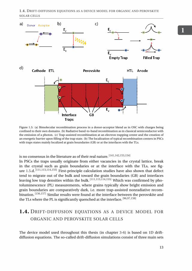
Band-to-band/bimolecular recombination corresponds to the direct recombination of afree electron from the conduction band (LUMO) with a free hole from the valence band(HOMO), see figure 1.5.a. The band-to-band denomination will be used when referringto perovskite and bimolecular when referring to organic semiconductors. This type ofrecombination is usually accompanied by the emission of a photon with the same energyas the bandgap and is, hence, also called radiative recombination. However, this is notalways the case, especially, in organic semiconductors, as that energy can be dispersedby other pathways that are nonradiative. [140–142]
1
11

1. INTRODUCTION
The band-to-band/bimolecular recombination rate (RB ) is given by
RB = γ (np −n2
i
), (1.1)
where n and p are electron and hole densities respectively, γ is the bimolecular recom-bination rate constant and ni is the intrinsic carrier concentration.In OCSs, γ is often written according to the reduced Langevin formula:
γ= γpr e ×γL = γpr e × q
ε
(µn +µp
)(1.2)
with γpr e the reduction factor for the Langevin law [143] that was introduced for the re-combination of ions in a gas. γpr e typically varies between 10−4 - 1 and γ between 10−11 -10−10 cm3 s-1. [144,145] Owing to the low mobility and dielectric constant of organic semi-conductors, bimolecular recombination is often found to be the dominant recombina-tion process in OSCs, [140,144] even though in new systems with NFAs this may not alwaysbe true.Perovskites, however, with their larger mobility and dielectric constant, do not suffer asmuch from band-to-band recombination, see figure 1.5.b. γ values typically range be-tween 10−11 - 10−9 cm3 s-1. [146–150] The low band-to-band recombination rate in PSCsmay be explained by lattice distortion leading to a spatial separation of electrons andholes decreasing the probability of charge carriers to recombine. [147] Instead, the recom-bination is mostly dominated by nonradiative recombination. [96–98,106]
1.3.2. TRAP-ASSISTED RECOMBINATION
Trap-assisted recombination consists of the recombination of an electron and a hole viaa localized state within the bandgap, see figure 1.5.c. Under steady-state conditions, thetrap-assisted recombination rate is usually described by the Shockley-Read-Hall (SRH)equation [151,152] such as:
RSRH = CnCpΣT
Cn(n +n1)+Cp (p +p1)
(np −ni
2) , (1.3)
where ΣT is the trap density, n1 and p1 are constants which depend on the trap energylevel (Etr ap ), and Cn and Cp are the capture coefficients for electrons and holes respec-tively. n1 and p1 are defined as followed:
n1 = Nc exp
(−EC −Etrap
kB T
)and p1 = Nv exp
(−Etrap −EV
kB T
)(1.4)
with kB the Boltzmann’s constant, T the absolute temperature, Nc and Nv the effectivedensity of states for the conduction and valence band respectively. In the remainder ofthis thesis we will consider in the simulations that Nc = Nv and only use the notationNc . The nature and origin of the trap in OSCs remain obscure. Several potential sourcesfor the trap states have been suggested such as impurities either from remaining fromsynthesis or due to the processing condition (atmosphere, solvent, additives...), struc-tural defects of the polymer or molecules,self-trapping and presence of water but there
1
12
1.4. DRIFT-DIFFUSION EQUATIONS AS A DEVICE MODEL FOR ORGANIC AND PEROVSKITE
SOLAR CELLS
Figure 1.5: (a) Bimolecular recombination process in a donor-acceptor blend as in OSC with charges beingconfined to their own domains. (b) Radiative band-to-band recombination as in classical semiconductor withthe emission of a photon. (c) Trap-assisted recombination at an electron trapping center and the creation ofan energetic barrier upon filling of the trap state. (b) The localization of typical recombination centers in PSCswith traps states mainly localized at grain boundaries (GB) or at the interfaces with the TLs.
is no consensus in the literature as of their real nature. [141,142,153,154]
In PSCs the traps usually originate from either vacancies in the crystal lattice, breakin the crystal such as grain boundaries or at the interface with the TLs, see fig-ure 1.5.d. [111,113,114,155] First-principle calculation studies have also shown that defecttend to migrate out of the bulk and toward the grain boundaries (GB) and interfacesleaving low trap densities within the bulk. [111,113,114,155] Which was confirmed by pho-toluminescence (PL) measurements, where grains typically show bright emission andgrain boundaries are comparatively dark, i.e. more trap-assisted nonradiative recom-bination. [156,157] Similar results were found at the interface between the perovskite andthe TLs where the PL is significantly quenched at the interface. [96,97,158]
1.4. DRIFT-DIFFUSION EQUATIONS AS A DEVICE MODEL FOR
ORGANIC AND PEROVSKITE SOLAR CELLS
The device model used throughout this thesis (in chapter 3-6) is based on 1D drift-diffusion equations. The so-called drift-diffusion simulations consist of three main sets
1
13

1. INTRODUCTION
of equations. The Poisson equation:
∂
∂x
(ε(x)
∂V (x)
∂x
)=−q
(p(x)−n(x)+Ci (x)
), (1.5)
with x is the position in the device,* V the electrostatic potential, n and p the elec-tron and hole concentrations, and ε the permittivity. Ci can represent any other typeof charges in the systems such as: (i) doping with N−
A and N+D being the ionized p-type
and n-type doping respectively, (ii) ions with Xc and Xa the cation and anion densitiesand (iii) the charged traps Σ+
T and Σ−T for hole and electron traps. Such as the Poisson
equation may be written as:
∂
∂x
(ε∂V
∂x
)=−q
(p −n +N+
D −N−A +Xc −Xa +Σ+
T −Σ−T
)(1.6)
The current continuity equations:
∂Jn
∂x=−q (G −R)
∂Jp
∂x= q (G −R)
(1.7)
with Jn,p the electron and hole currents, G and R the generation and recombination raterespectively. The movement of these free charges is governed either by diffusion due to agradient in carrier density or by drift following the electric field such as the electron andhole currents can be written as: [159]
Jn =−qnµn∂V
∂x+qDn
∂n
∂x
Jp =−qpµp∂V
∂x−qDp
∂p
∂x
(1.8)
withµn,p the charge carrier mobilities and Dn,p carrier diffusion coefficients. The carrierdiffusion coefficients can be written following Einstein equation such as: [159]
Dn,p =µn,pVT (1.9)
with VT = kB T /q the thermal voltage (VT = 25.69 mV at 25°C – 298.15 K).For the simulation we chose to place the cathode at x = 0 and the anode at x = L asa convention, L being the total thickness of the device. If necessary, additional layerswith different properties (mobility, doping, dielectric constant...) can be added to thesimulation to reproduce, for example, a typical solar cell stack as shown in figure 1.5.d.In order to numerically solve the system of equation presented above we need to specifythe boundary conditions for the carrier densities:
n(0) = Nc exp
(−φn
VT
)n(L) = Nc exp
(−Eg −φp
VT
)p(0) = Nv exp
(−Eg −φn
VT
)p(L) = Nv exp
(−φp
VT
) (1.10)
*Note that for notation convenience the x dependence of the variables will be dropped in the remainder of thisthesis. However, in a multilayer stack not only densities values are meant to vary with x but also values suchas mobilities and dielectric constant...
1
14

REFERENCES
and the potential at the contacts:
q(V (L)−V (0)+Vapp
)=Wc −Wa (1.11)
with φn and φp the electron and hole injection barrier at the cathode and anode, Vapp
being the externally applied voltage and Wa and Wc the anode and cathode work func-tions respectively. The built-in potential is then given by Vbi = (Wc −Wa)/q . Note thatthe Eg in equation 1.10 may not necessarily be the same if there are different layers incontact with the cathode and the anode.The generation rate of charge G , in equation 1.7, is usually obtained by measuring thecomplex refractive index of all the layers and performing transfer matrix modeling. [160]
As for the recombination rate R, it is typically expressed by adding the contributionfrom the band-to-band/bimolecular recombination and SRH recombination from equa-tions 1.1 and 1.3. More details on the numerical methods used to solve this system ofequations can be found in Ref. 106,159,161–163.
REFERENCES[1] M. Nicholson, The Power makers’ challenge: And the need for fission energy, Green
Energy and Technology (Springer London, 2012).
[2] I. Hore-Lacy, World Nuclear Association, and World Nuclear University, NuclearEnergy in the 21st Century : World Nuclear University Press. (Academic Press, 2006).
[3] J. D. Sterman, L. Siegel, and J. N. Rooney-Varga, Does replacing coal with woodlower CO2 emissions? Dynamic lifecycle analysis of wood bioenergy, Environmen-tal Research Letters 13, 015007 (2018).
[4] P. R. Shukla, J. Skea, E. Calvo Buendia, V. Masson-Delmotte, H.-O. Pörtner, D. C.Roberts, P. Zhai, R. Slade, S. Connors, R. van Diemen, M. Ferrat, E. Haughey, S. Luz,S. Neogi, M. Pathak, J. Petzold, J. Portugal Pereira, P. Vyas, E. Huntley, K. Kissick,M. Belkacemi, J. Malley, and (eds.), Climate Change and Land: an IPCC spe-cial report on climate change, desertification, land degradation, sustainable landmanagement, food security, and greenhouse gas fluxes in terrestrial ecosystems,https://www.ipcc.ch/srccl/ (2019), accessed: 2020-01-15.
[5] M. Collins, R. Knutti, J. Arblaster, J.-L. Dufresne, T. Fichefet, P. Friedlingstein,X. Gao, W. Gutowski, T. Johns, G. Krinner, M. Shongwe, C. Tebaldi, A. Weaver,and M. Wehner, Long-term Climate Change: Projections, Commitments and Irre-versibility. In: Climate Change 2013: The Physical Science Basis. Contribution ofWorking Group I to the Fifth Assessment Report of the Intergovernmental Panelon Climate Change, https://www.ipcc.ch/site/assets/uploads/2018/02/WG1AR5_Chapter12_FINAL.pdf (2013), accessed: 2020-01-15.
[6] BP Statistical Review of World Energy 68th Edition, https://www.bp.com/content/dam/bp/business-sites/en/global/corporate/pdfs/energy-economics/statistical-review/bp-stats-review-2019-full-report.pdf (2019), accessed: 2020-01-15.
1
15

1. INTRODUCTION
[7] IEA report, Renewables 2019, https://www.iea.org/reports/renewables-2019 (2019).
[8] Fraunhofer ISE report, https://www.ise.fraunhofer.de/content/dam/ise/de/documents/publications/studies/Photovoltaics-Report.pdf (2019).
[9] V. Sivaram, J. O. Dabiri, and D. M. Hart, The Need for Continued Innovation inSolar, Wind, and Energy Storage, Joule 2, 1639 (2018).
[10] V. Sivaram and S. Kann, Solar power needs a more ambitious cost target, NatureEnergy 1, 16036 (2016).
[11] NREL, Best research-cell efficiencies, https://www.nrel.gov/pv/assets/pdfs/best-research-cell-efficiencies.20191106.pdf (2020), accessed: 2020-01-16.
[12] W. Shockley and H. J. Queisser, Detailed balance limit of efficiency of p-n junctionsolar cells, Journal of Applied Physics 32, 510 (1961).
[13] K. Lee, N. Kim, K. Kim, H. D. Um, W. Jin, D. Choi, J. Park, K. J. Park, S. Lee, andK. Seo, Neutral-Colored Transparent Crystalline Silicon Photovoltaics, Joule 4, 235(2020).
[14] N. El-Atab, N. Qaiser, R. Bahabry, and M. M. Hussain, Corrugation Enabled Asym-metrically Ultrastretchable (95%) Monocrystalline Silicon Solar Cells with High Ef-ficiency (19%), Advanced Energy Materials 9, 1902883 (2019).
[15] R. Xia, C. J. Brabec, H.-L. Yip, and Y. Cao, High-Throughput OpticalScreening for Efficient Semitransparent Organic Solar Cells, Joule (2019),10.1016/J.JOULE.2019.06.016.
[16] Q. Xue, R. Xia, C. J. Brabec, and H. L. Yip, Recent advances in semi-transparentpolymer and perovskite solar cells for power generating window applications, En-ergy and Environmental Science 11, 1688 (2018).
[17] T. Yan, W. Song, J. Huang, R. Peng, L. Huang, and Z. Ge, 16.67% Rigid and 14.06%Flexible Organic Solar Cells Enabled by Ternary Heterojunction Strategy, AdvancedMaterials 31 (2019), 10.1002/adma.201902210.
[18] D. Koo, S. Jung, J. Seo, G. Jeong, Y. Choi, J. Lee, S. M. Lee, Y. Cho, M. Jeong, J. Lee,J. Oh, C. Yang, and H. Park, Flexible Organic Solar Cells Over 15% Efficiency withPolyimide-Integrated Graphene Electrodes, Joule 4, 1021 (2020).
[19] L. Yuan, Z. Wang, R. Duan, P. Huang, K. Zhang, Q. Chen, N. K. Allam, Y. Zhou,B. Song, and Y. Li, Semi-transparent perovskite solar cells: Unveiling the trade-off between transparency and efficiency, Journal of Materials Chemistry A 6, 19696(2018).
1
16

REFERENCES
[20] C. Roldán-Carmona, O. Malinkiewicz, R. Betancur, G. Longo, C. Momblona,F. Jaramillo, L. Camacho, and H. J. Bolink, High efficiency single-junction semi-transparent perovskite solar cells, Energy and Environmental Science 7, 2968(2014).
[21] F. Fu, T. Feurer, T. Jäger, E. Avancini, B. Bissig, S. Yoon, S. Buecheler, and A. N. Ti-wari, Low-temperature-processed efficient semi-transparent planar perovskite solarcells for bifacial and tandem applications, Nature Communications 6, 1 (2015).
[22] X. Hu, X. Meng, L. Zhang, Y. Zhang, Z. Cai, Z. Huang, M. Su, Y. Wang, M. Li, F. Li,X. Yao, F. Wang, W. Ma, Y. Chen, and Y. Song, A Mechanically Robust ConductingPolymer Network Electrode for Efficient Flexible Perovskite Solar Cells, Joule 3, 2205(2019).
[23] D. Yang, R. Yang, S. Priya, and S. F. Liu, Recent Advances in Flexible Perovskite SolarCells: Fabrication and Applications, Angewandte Chemie - International Edition58, 4466 (2019).
[24] P. Atkins and J. de Paula, Physical Chemistry (W. H. Freeman Company, New York,2006).
[25] A. Köhler and H. Bässler, Electronic Processes in Organic Semiconductors: An Intro-duction (Wiley-VCH Verlag, Weinheim, Germany, 2015).
[26] O. V. Mikhnenko, P. W. Blom, and T. Q. Nguyen, Exciton diffusion in organic semi-conductors, Energy and Environmental Science 8, 1867 (2015).
[27] B. Schweitzer and H. Bässler, Excitons in conjugated polymers, Synthetic Metals109, 1 (2000).
[28] B. A. Gregg, Excitonic solar cells, Journal of Physical Chemistry B 107, 4688 (2003).
[29] S. R. Forrest, Excitons and the lifetime of organic semiconductor devices, Philosoph-ical Transactions of the Royal Society A: Mathematical, Physical and EngineeringSciences, 373 (2015), 10.1098/rsta.2014.0320.
[30] S. E. Shaheen, C. J. Brabec, N. S. Sariciftci, F. Padinger, T. Fromherz, and J. C.Hummelen, 2.5% efficient organic plastic solar cells, Applied Physics Letters 78,841 (2001).
[31] M. A. Loi, S. Toffanin, M. Muccini, M. Forster, U. Scherf, and M. Scharber,Charge Transfer Excitons in Bulk Heterojunctions of a Polyfluorene Copolymer anda Fullerene Derivative, Advanced Functional Materials 17, 2111 (2007).
[32] C. Deibel, T. Strobel, and V. Dyakonov, Role of the Charge Transfer State in OrganicDonor-Acceptor Solar Cells, Advanced Materials 22, 4097 (2010).
[33] K. Vandewal, J. Widmer, T. Heumueller, C. J. Brabec, M. D. McGehee, K. Leo,M. Riede, and A. Salleo, Increased Open-Circuit Voltage of Organic Solar Cells byReduced Donor-Acceptor Interface Area, Advanced Materials 26, 3839 (2014).
1
17

1. INTRODUCTION
[34] K. Vandewal, S. Albrecht, E. T. Hoke, K. R. Graham, J. Widmer, J. D. Douglas,M. Schubert, W. R. Mateker, J. T. Bloking, G. F. Burkhard, A. Sellinger, J. M. Fréchet,A. Amassian, M. K. Riede, M. D. McGehee, D. Neher, and A. Salleo, Efficient chargegeneration by relaxed charge-transfer states at organic interfaces, Nature Materials13, 63 (2014).
[35] D. Qian, Z. Zheng, H. Yao, W. Tress, T. R. Hopper, S. Chen, S. Li, J. Liu, S. Chen,J. Zhang, X. K. Liu, B. Gao, L. Ouyang, Y. Jin, G. Pozina, I. A. Buyanova, W. M. Chen,O. Inganäs, V. Coropceanu, J. L. Bredas, H. Yan, J. Hou, F. Zhang, A. A. Bakulin, andF. Gao, Design rules for minimizing voltage losses in high-efficiency organic solarcells, Nature Materials 17, 703 (2018).
[36] S. Li, L. Zhan, C. Sun, H. Zhu, G. Zhou, W. Yang, M. Shi, C.-Z. Li, J. Hou, Y. Li, andH. Chen, Highly Efficient Fullerene-Free Organic Solar Cells Operate at Near ZeroHighest Occupied Molecular Orbital Offsets, Journal of the American Chemical So-ciety 141, 3073 (2019).
[37] L. Perdigón-Toro, H. Zhang, A. Markina, J. Yuan, S. M. Hosseini, C. M. Wolff, G. Zuo,M. Stolterfoht, Y. Zou, F. Gao, D. Andrienko, S. Shoaee, and D. Neher, Barrier-less Free Charge Generation in the High-Performance PM6:Y6 Bulk HeterojunctionNon-Fullerene Solar Cell, Advanced Materials 32, 1906763 (2020).
[38] W. Chen, T. Xu, F. He, W. Wang, C. Wang, J. Strzalka, Y. Liu, J. Wen, D. J. Miller,J. Chen, K. Hong, L. Yu, and S. B. Darling, Hierarchical nanomorphologies promoteexciton dissociation in polymer/fullerene bulk heterojunction solar cells, Nano Let-ters 11, 3707 (2011).
[39] F. Paquin, G. Latini, M. Sakowicz, P. L. Karsenti, L. Wang, D. Beljonne, N. Stin-gelin, and C. Silva, Charge separation in semicrystalline polymeric semiconductorsby photoexcitation: Is the mechanism intrinsic or extrinsic? Physical Review Letters106, 197401 (2011).
[40] T. M. Burke and M. D. McGehee, How High Local Charge Carrier Mobility and anEnergy Cascade in a Three-Phase Bulk Heterojunction Enable >90% Quantum Effi-ciency, Advanced Materials 26, 1923 (2014).
[41] S. Sweetnam, K. R. Graham, G. O. Ngongang Ndjawa, T. Heumüller, J. A. Bartelt,T. M. Burke, W. Li, W. You, A. Amassian, and M. D. McGehee, Characterization ofthe polymer energy landscape in polymer:fullerene bulk heterojunctions with pureand mixed phases, Journal of the American Chemical Society 136, 14078 (2014).
[42] A. Miller and E. Abrahams, Impurity conduction at low concentrations, PhysicalReview 120, 745 (1960).
[43] R. A. Marcus and N. Sutin, Bba reviews on bioenergetics, 811, 265 (1985).
[44] H. Bässler, Charge Transport in Disordered Organic Photoconductors a Monte CarloSimulation Study, physica status solidi (b) 175, 15 (1993).
1
18

REFERENCES
[45] C. W. Tang, Two-layer organic photovoltaic cell, Applied Physics Letters 48, 183(1986).
[46] G. Yu, J. Gao, J. C. Hummelen, F. Wudl, and A. J. Heeger, Polymer photovoltaiccells: Enhanced efficiencies via a network of internal donor-acceptor heterojunc-tions, Science 270, 1789 (1995).
[47] Q. Liu, Y. Jiang, K. Jin, J. Qin, J. Xu, W. Li, J. Xiong, J. Liu, Z. Xiao, K. Sun, S. Yang,X. Zhang, and L. Ding, 18% Efficiency organic solar cells, Science Bulletin (2020),10.1016/j.scib.2020.01.001.
[48] Y. Firdaus, V. M. Le Corre, J. I. Khan, Z. Kan, F. Laquai, P. M. Beaujuge, and T. D. An-thopoulos, Key Parameters Requirements for Non-Fullerene-Based Organic SolarCells with Power Conversion Efficiency >20%, Advanced Science 6, 1802028 (2019).
[49] M. O. Reese, S. A. Gevorgyan, M. Jørgensen, E. Bundgaard, S. R. Kurtz, D. S. Ginley,D. C. Olson, M. T. Lloyd, P. Morvillo, E. A. Katz, A. Elschner, O. Haillant, T. R. Currier,V. Shrotriya, M. Hermenau, M. Riede, K. R. Kirov, G. Trimmel, T. Rath, O. Inganäs,F. Zhang, M. Andersson, K. Tvingstedt, M. Lira-Cantu, D. Laird, C. McGuiness,S. Gowrisanker, M. Pannone, M. Xiao, J. Hauch, R. Steim, D. M. Delongchamp,R. Rösch, H. Hoppe, N. Espinosa, A. Urbina, G. Yaman-Uzunoglu, J. B. Bonekamp,A. J. Van Breemen, C. Girotto, E. Voroshazi, and F. C. Krebs, Consensus stabilitytesting protocols for organic photovoltaic materials and devices, Solar Energy Ma-terials and Solar Cells 95, 1253 (2011).
[50] A. Distler, T. Sauermann, H.-J. Egelhaaf, S. Rodman, D. Waller, K.-S. Cheon, M. Lee,and D. M. Guldi, The Effect of PCBM Dimerization on the Performance of Bulk Het-erojunction Solar Cells, Advanced Energy Materials 4, 1300693 (2014).
[51] W. R. Mateker and M. D. McGehee, Progress in Understanding Degradation Mech-anisms and Improving Stability in Organic Photovoltaics, Advanced Materials 29,1603940 (2017).
[52] N. Y. Doumon, G. Wang, R. C. Chiechi, and L. J. A. Koster, Relating polymer chem-ical structure to the stability of polymer:fullerene solar cells, Journal of MaterialsChemistry C 5, 6611 (2017).
[53] N. Y. Doumon, M. V. Dryzhov, F. V. Houard, V. M. Le Corre, A. Rahimi Chatri,P. Christodoulis, and L. J. A. Koster, Photostability of Fullerene and Non-FullerenePolymer Solar Cells: The Role of the Acceptor, ACS Applied Materials & Interfaces11, 8310 (2019).
[54] N. Y. Doumon, F. V. Houard, J. Dong, P. Christodoulis, M. V. Dryzhov, G. Portale,and L. J. A. Koster, Improved photostability in ternary blend organic solar cells: Therole of [70]PCBM, Journal of Materials Chemistry C 7, 5104 (2019).
[55] N. Y. Doumon, F. V. Houard, J. Dong, H. Yao, G. Portale, J. Hou, and L. J. A. Koster,Energy level modulation of ITIC derivatives: Effects on the photodegradation of con-ventional and inverted organic solar cells, Organic Electronics 69, 255 (2019).
1
19
1. INTRODUCTION
[56] N. Y. Doumon and L. J. A. Koster, Effects of the Reduction and/or Fluorination ofthe TT-Units in BDT-TT Polymers on the Photostability of Polymer:Fullerene SolarCells, Solar RRL 3, 1800301 (2019).
[57] N. Y. Doumon, G. Wang, X. Qiu, A. J. Minnaard, R. C. Chiechi, and L. J. A. Koster,1,8-diiodooctane acts as a photo-acid in organic solar cells, Scientific Reports 9, 1(2019).
[58] C. Zhang, T. Heumueller, S. Leon, W. Gruber, K. Burlafinger, X. Tang, J. D. Perea,I. Wabra, A. Hirsch, T. Unruh, N. Li, and C. J. Brabec, A top-down strategy identify-ing molecular phase stabilizers to overcome microstructure instabilities in organicsolar cells, Energy and Environmental Science 12, 1078 (2019).
[59] O. R. Yamilova, I. V. Martynov, A. S. Brandvold, I. V. Klimovich, A. H. Balzer, A. V.Akkuratov, I. E. Kusnetsov, N. Stingelin, and P. A. Troshin, What is Killing OrganicPhotovoltaics: Light-Induced Crosslinking as a General Degradation Pathway ofOrganic Conjugated Molecules, Advanced Energy Materials , 1903163 (2020).
[60] M. A. Green, E. D. Dunlop, J. Hohl-Ebinger, M. Yoshita, N. Kopidakis, and A. W.Ho-Baillie, Solar cell efficiency tables (Version 28-55), Progress in Photovoltaics:Research and Applications 28, 3 (2020).
[61] L. Dou, J. You, J. Yang, C. C. Chen, Y. He, S. Murase, T. Moriarty, K. Emery, G. Li, andY. Yang, Tandem polymer solar cells featuring a spectrally matched low-bandgappolymer, Nature Photonics 6, 180 (2012).
[62] J. Zhao, Y. Li, G. Yang, K. Jiang, H. Lin, H. Ade, W. Ma, and H. Yan, Efficient organicsolar cells processed from hydrocarbon solvents, Nature Energy 1, 15027 (2016).
[63] Z. Xiao, X. Jia, and L. Ding, Ternary organic solar cells offer 14% power conversionefficiency, Science Bulletin 62, 1562 (2017).
[64] W. Zhao, S. Li, H. Yao, S. Zhang, Y. Zhang, B. Yang, and J. Hou, Molecular Optimiza-tion Enables over 13% Efficiency in Organic Solar Cells, Journal of the AmericanChemical Society 139, 7148 (2017).
[65] S. Zhang, Y. Qin, J. Zhu, and J. Hou, Over 14% Efficiency in Polymer Solar CellsEnabled by a Chlorinated Polymer Donor, Advanced Materials , 1800868 (2018).
[66] X. Che, Y. Li, Y. Qu, and S. R. Forrest, High fabrication yield organic tandem pho-tovoltaics combining vacuum- and solution-processed subcells with 15% efficiency,Nature Energy 3, 422 (2018).
[67] L. Meng, Y. Zhang, X. Wan, C. Li, X. Zhang, Y. Wang, X. Ke, Z. Xiao, L. Ding, R. Xia,H.-L. Yip, Y. Cao, and Y. Chen, Organic and solution-processed tandem solar cellswith 17.3% efficiency. Science (New York, N.Y.) , eaat2612 (2018).
[68] J. Yuan, Y. Zhang, L. Zhou, G. Zhang, H. L. Yip, T. K. Lau, X. Lu, C. Zhu, H. Peng,P. A. Johnson, M. Leclerc, Y. Cao, J. Ulanski, Y. Li, and Y. Zou, Single-Junction Or-ganic Solar Cell with over 15% Efficiency Using Fused-Ring Acceptor with Electron-Deficient Core, Joule 3, 1140 (2019).
1
20

REFERENCES
[69] Y. Cui, H. Yao, J. Zhang, T. Zhang, Y. Wang, L. Hong, K. Xian, B. Xu, S. Zhang, J. Peng,Z. Wei, F. Gao, and J. Hou, Over 16% efficiency organic photovoltaic cells enabledby a chlorinated acceptor with increased open-circuit voltages, Nature Communi-cations 10, 2515 (2019).
[70] Y. Lin, B. Adilbekova, Y. Firdaus, E. Yengel, H. Faber, M. Sajjad, X. Zheng, E. Yarali,A. Seitkhan, O. M. Bakr, A. El-Labban, U. Schwingenschlögl, V. Tung, I. McCulloch,F. Laquai, and T. D. Anthopoulos, 17% Efficient Organic Solar Cells Based on LiquidExfoliated WS 2 as a Replacement for PEDOT:PSS, Advanced Materials 31, 1902965(2019).
[71] Asca by armor, https://www.asca.com/, accessed: 12-02-2020.
[72] Heliatek, https://www.heliatek.com/, accessed: 12-02-2020.
[73] Opvius, http://www.opvius.com/, accessed: 12-02-2020.
[74] B. Fan, W. Zhong, L. Ying, D. Zhang, M. Li, Y. Lin, R. Xia, F. Liu, H. L. Yip, N. Li,Y. Ma, C. J. Brabec, F. Huang, and Y. Cao, Surpassing the 10% efficiency milestonefor 1-cm2 all-polymer solar cells, Nature Communications 10, 1 (2019).
[75] J. E. Carlé, M. Helgesen, O. Hagemann, M. Hö, I. M. Heckler, E. Bundgaard,S. A. Gevorgyan, R. R. Søndergaard, M. Jørgensen, R. García-Valverde, S. Chaouki-Almagro, J. A. Villarejo, and F. C. Krebs, Overcoming the Scaling Lag for PolymerSolar Cells, (2017), 10.1016/j.joule.2017.08.002.
[76] S. Dong, K. Zhang, B. Xie, J. Xiao, H.-L. Yip, H. Yan, F. Huang, and Y. Cao, High-Performance Large-Area Organic Solar Cells Enabled by Sequential Bilayer Process-ing via Nonhalogenated Solvents, Advanced Energy Materials 9, 1802832 (2019).
[77] F. C. Krebs, T. Tromholt, and M. Jørgensen, Upscaling of polymer solar cell fabrica-tion using full roll-to-roll processing, Nanoscale 2, 873 (2010).
[78] Roll-to-roll fabrication of polymer solar cells, Materials Today 15, 36 (2012).
[79] J. Yang, Y. Lin, W. Zheng, A. Liu, W. Cai, X. Yu, F. Zhang, Q. Liang, H. Wu, D. Qin,and L. Hou, Roll-to-Roll Slot-Die-Printed Polymer Solar Cells by Self-Assembly, ACSApplied Materials and Interfaces 10, 22485 (2018).
[80] G. Wang, M. A. Adil, J. Zhang, and Z. Wei, Large-Area Organic Solar Cells: Ma-terial Requirements, Modular Designs, and Printing Methods, Advanced Materials31, 1805089 (2019).
[81] J. Lee, Y. Seo, S. Kwon, D. Kim, S. Jang, H. Jung, Y. Lee, H. Weerasinghe, T. Kim,J. Y. Kim, D. Vak, and S. Na, Slot-Die and Roll-to-Roll Processed Single JunctionOrganic Photovoltaic Cells with the Highest Efficiency, Advanced Energy Materials9, 1901805 (2019).
[82] D. Weber, CH3NH3PbX3, ein Pb(II)-System mit kubischer Perowskitstruktur,Zeitschrift fur Naturforschung - Section B Journal of Chemical Sciences 33, 1443(1978).
1
21

1. INTRODUCTION
[83] A. Kojima, K. Teshima, Y. Shirai, and T. Miyasaka, Organometal Halide Perovskitesas Visible-Light Sensitizers for Photovoltaic Cells, Journal of the American ChemicalSociety 131, 6050 (2009).
[84] M. M. Lee, J. Teuscher, T. Miyasaka, T. N. Murakami, and H. J. Snaith, EfficientHybrid Solar Cells Based on Meso-Superstructured Organometal Halide Perovskites,Science 338, 643 (2012).
[85] H.-S. Kim, C.-R. Lee, J.-H. Im, K.-B. Lee, T. Moehl, A. Marchioro, S.-J. Moon,R. Humphry-Baker, J.-H. Yum, J. E. Moser, M. Grätzel, and N.-G. Park, Lead Io-dide Perovskite Sensitized All-Solid-State Submicron Thin Film Mesoscopic SolarCell with Efficiency Exceeding 9%, Scientific Reports 2, 591 (2012).
[86] E. T. Hoke, D. J. Slotcavage, E. R. Dohner, A. R. Bowring, H. I. Karunadasa, andM. D. McGehee, Reversible photo-induced trap formation in mixed-halide hybridperovskites for photovoltaics, Chemical Science 6, 613 (2015).
[87] F. Brivio, K. T. Butler, A. Walsh, and M. Van Schilfgaarde, Relativistic quasiparti-cle self-consistent electronic structure of hybrid halide perovskite photovoltaic ab-sorbers, Physical Review B - Condensed Matter and Materials Physics 89, 155204(2014).
[88] C. Motta, F. El-Mellouhi, and S. Sanvito, Charge carrier mobility in hybrid halideperovskites, Scientific Reports 5, 12746 (2015).
[89] T. Wang, B. Daiber, J. M. Frost, S. A. Mann, E. C. Garnett, A. Walsh, and B. Ehrler,Indirect to direct bandgap transition in methylammonium lead halide perovskite,Energy and Environmental Science 10, 509 (2017).
[90] V. Sarritzu, N. Sestu, D. Marongiu, X. Chang, Q. Wang, S. Masi, S. Colella, A. Rizzo,A. Gocalinska, E. Pelucchi, M. L. Mercuri, F. Quochi, M. Saba, A. Mura, and G. Bon-giovanni, Direct or Indirect Bandgap in Hybrid Lead Halide Perovskites? AdvancedOptical Materials 6, 1701254 (2018).
[91] L. M. Herz, Charge-Carrier Mobilities in Metal Halide Perovskites: FundamentalMechanisms and Limits, ACS Energy Letters 2, 1539 (2017).
[92] N. Onoda-Yamamuro, T. Matsuo, and H. Suga, Dielectric study of CH3NH3PbX3 (X= Cl, Br, I), Journal of Physics and Chemistry of Solids 53, 935 (1992).
[93] J. M. Frost, K. T. Butler, F. Brivio, C. H. Hendon, M. Van Schilfgaarde, and A. Walsh,Atomistic origins of high-performance in hybrid halide perovskite solar cells, NanoLetters 14, 2584 (2014).
[94] L. M. Herz, How Lattice Dynamics Moderate the Electronic Properties of Metal-Halide Perovskites, Journal of Physical Chemistry Letters 9, 6853 (2018).
[95] J. N. Wilson, J. M. Frost, S. K. Wallace, and A. Walsh, Dielectric and ferroic proper-ties of metal halide perovskites, APL Materials 7, 010901 (2019).
1
22

REFERENCES
[96] M. Stolterfoht, C. M. Wolff, J. A. Márquez, S. Zhang, C. J. Hages, D. Rothhardt, S. Al-brecht, P. L. Burn, P. Meredith, T. Unold, and D. Neher, Visualization and suppres-sion of interfacial recombination for high-efficiency large-area pin perovskite solarcells, Nature Energy 3, 847 (2018).
[97] M. Stolterfoht, P. Caprioglio, C. M. Wolff, J. A. Márquez, J. Nordmann, S. Zhang,D. Rothhardt, U. Hörmann, Y. Amir, A. Redinger, L. Kegelmann, F. Zu, S. Albrecht,N. Koch, T. Kirchartz, M. Saliba, T. Unold, and D. Neher, The impact of energyalignment and interfacial recombination on the internal and external open-circuitvoltage of perovskite solar cells, Energy and Environmental Science 12, 2778 (2019).
[98] V. M. Le Corre, M. Stolterfoht, L. Perdigón Toro, M. Feuerstein, C. Wolff, L. Gil-Escrig, H. J. Bolink, D. Neher, and L. J. A. Koster, Charge Transport Layers Limitingthe Efficiency of Perovskite Solar Cells: How To Optimize Conductivity, Doping, andThickness, ACS Applied Energy Materials 2, 6280 (2019).
[99] H. J. Snaith, A. Abate, J. M. Ball, G. E. Eperon, T. Leijtens, N. K. Noel, S. D. Stranks,J. T. W. Wang, K. Wojciechowski, and W. Zhang, Anomalous hysteresis in perovskitesolar cells, Journal of Physical Chemistry Letters 5, 1511 (2014).
[100] E. L. Unger, E. T. Hoke, C. D. Bailie, W. H. Nguyen, A. R. Bowring, T. Heumüller,M. G. Christoforo, and M. D. McGehee, Hysteresis and transient behavior incurrent–voltage measurements of hybrid-perovskite absorber solar cells, Energy &Environmental Sciences 7, 3690 (2014).
[101] W. Tress, N. Marinova, T. Moehl, S. M. Zakeeruddin, M. K. Nazeeruddin, andM. Grätzel, Understanding the rate-dependent J–V hysteresis, slow time component,and aging in CH3NH3PbI3 perovskite solar cells: the role of a compensated electricfield, Energy & Environmental Sciences 8, 995 (2015).
[102] G. Richardson, S. E. O’Kane, R. G. Niemann, T. A. Peltola, J. M. Foster, P. J. Cameron,and A. B. Walker, Can slow-moving ions explain hysteresis in the current–voltagecurves of perovskite solar cells? Energy & Environmental Sciences 9, 1476 (2016).
[103] N. Tessler and Y. Vaynzof, Preventing hysteresis in perovskite solar cells by undopedcharge blocking layers, ACS Applied Energy Materials 1, 676 (2018).
[104] S. A. L. Weber, I. M. Hermes, S.-H. Turren-Cruz, C. Gort, V. W. Bergmann, L. Gilson,A. Hagfeldt, M. Graetzel, W. Tress, and R. Berger, How the formation of interfa-cial charge causes hysteresis in perovskite solar cells, Energy Environ. Sci. 11, 2404(2018).
[105] J. Mizusaki, K. Arai, and K. Fueki, Ionic conduction of the perovskite-type halides,Solid State Ionics 11, 203 (1983).
[106] T. S. Sherkar, C. Momblona, L. Gil-Escrig, J. Ávila, M. Sessolo, H. J. Bolink, andL. J. A. Koster, Recombination in perovskite solar cells: Significance of grain bound-aries, interface traps and defect ions, ACS Energy Letters 2, 1214 (2017).
1
23

1. INTRODUCTION
[107] C. Li, A. Guerrero, Y. Zhong, and S. Huettner, Origins and mechanisms of hystere-sis in organometal halide perovskites, Journal of Physics: Condensed Matter 29,193001 (2017).
[108] M. H. Futscher, J. M. Lee, L. McGovern, L. A. Muscarella, T. Wang, M. I. Haider,A. Fakharuddin, L. Schmidt-Mende, and B. Ehrler, Quantification of ion migra-tion in CH3NH3PbI3 perovskite solar cells by transient capacitance measurements,Materials Horizons 6, 1497 (2019).
[109] M. H. Futscher, M. K. Gangishetty, D. N. Congreve, and B. Ehrler, Quantifyingmobile ions and electronic defects in perovskite-based devices with temperature-dependent capacitance measurements: Frequency vs time domain, Journal ofChemical Physics 152, 044202 (2020).
[110] L. Bertoluzzi, C. C. Boyd, N. Rolston, J. Xu, R. Prasanna, B. C. O’Regan, and M. D.McGehee, Mobile Ion Concentration Measurement and Open-Access Band Dia-gram Simulation Platform for Halide Perovskite Solar Cells, Joule 4, 109 (2020).
[111] J. M. Azpiroz, E. Mosconi, J. Bisquert, and F. De Angelis, Defect migration in methy-lammonium lead iodide and its role in perovskite solar cell operation, Energy &Environmental Science 8, 2118 (2015).
[112] J. Haruyama, K. Sodeyama, L. Han, and Y. Tateyama, First-principles study of iondiffusion in perovskite solar cell sensitizers, Journal of the American Chemical So-ciety 137, 10048 (2015).
[113] P. Delugas, C. Caddeo, A. Filippetti, and A. Mattoni, Thermally Activated PointDefect Diffusion in Methylammonium Lead Trihalide: Anisotropic and UltrahighMobility of Iodine, Journal of Physical Chemistry Letters 7, 2356 (2016).
[114] C. Eames, J. M. Frost, P. R. Barnes, B. C. O’Regan, A. Walsh, and M. S. Islam, Ionictransport in hybrid lead iodide perovskite solar cells, Nature Communications 6, 1(2015).
[115] P. Calado, A. M. Telford, D. Bryant, X. Li, J. Nelson, B. C. O’Regan, and P. R. Barnes,Evidence for ion migration in hybrid perovskite solar cells with minimal hysteresis,Nature Communications 7, 13831 (2016).
[116] M. T. Neukom, A. Schiller, S. Züfle, E. Knapp, J. Ávila, D. Pérez-del Rey, C. Dreessen,K. P. Zanoni, M. Sessolo, H. J. Bolink, and B. Ruhstaller, Consistent Device Simu-lation Model Describing Perovskite Solar Cells in Steady-State, Transient, and Fre-quency Domain, ACS Applied Materials & Interfaces 11, 23320 (2019).
[117] M. T. Neukom, S. Züfle, E. Knapp, M. Makha, R. Hany, and B. Ruhstaller, Why per-ovskite solar cells with high efficiency show small IV-curve hysteresis, Solar EnergyMaterials and Solar Cells 169, 159 (2017).
[118] M. V. Khenkin, E. A. Katz, A. Abate, G. Bardizza, J. J. Berry, C. Brabec, F. Brunetti,V. Bulovic, Q. Burlingame, A. Di Carlo, R. Cheacharoen, Y. B. Cheng, A. Colsmann,
1
24

REFERENCES
S. Cros, K. Domanski, M. Dusza, C. J. Fell, S. R. Forrest, Y. Galagan, D. Di Giro-lamo, M. Grätzel, A. Hagfeldt, E. von Hauff, H. Hoppe, J. Kettle, H. Köbler, M. S.Leite, S. F. Liu, Y. L. Loo, J. M. Luther, C. Q. Ma, M. Madsen, M. Manceau, M. Math-eron, M. McGehee, R. Meitzner, M. K. Nazeeruddin, A. F. Nogueira, Ç. Odabası,A. Osherov, N. G. Park, M. O. Reese, F. De Rossi, M. Saliba, U. S. Schubert, H. J.Snaith, S. D. Stranks, W. Tress, P. A. Troshin, V. Turkovic, S. Veenstra, I. Visoly-Fisher,A. Walsh, T. Watson, H. Xie, R. Yıldırım, S. M. Zakeeruddin, K. Zhu, and M. Lira-Cantu, Consensus statement for stability assessment and reporting for perovskitephotovoltaics based on ISOS procedures, Nature Energy 5, 35 (2020).
[119] K. A. Bush, A. F. Palmstrom, Z. J. Yu, M. Boccard, R. Cheacharoen, J. P. Mailoa,D. P. McMeekin, R. L. Hoye, C. D. Bailie, T. Leijtens, I. M. Peters, M. C. Minichetti,N. Rolston, R. Prasanna, S. Sofia, D. Harwood, W. Ma, F. Moghadam, H. J. Snaith,T. Buonassisi, Z. C. Holman, S. F. Bent, and M. D. McGehee, 23.6%-efficient mono-lithic perovskite/silicon tandem solar cells with improved stability, Nature Energy2, 1 (2017).
[120] F. Sahli, J. Werner, B. A. Kamino, M. Bräuninger, R. Monnard, B. Paviet-Salomon,L. Barraud, L. Ding, J. J. Diaz Leon, D. Sacchetto, G. Cattaneo, M. Despeisse,M. Boccard, S. Nicolay, Q. Jeangros, B. Niesen, and C. Ballif, Fully textured mono-lithic perovskite/silicon tandem solar cells with 25.2% power conversion efficiency,Nature Materials 17, 820 (2018).
[121] Oxford pv, https://www.oxfordpv.com/, accessed: 26-02-2020.
[122] Solliance, https://www.solliance.eu/ (), accessed: 26-02-2020.
[123] Wonder solar, http://www.wondersolar.cn//, accessed: 26-02-2020.
[124] Saule technologies, https://sauletech.com/ (), accessed: 26-02-2020.
[125] Q. Jiang, Y. Zhao, X. Zhang, X. Yang, Y. Chen, Z. Chu, Q. Ye, X. Li, Z. Yin, and J. You,Surface passivation of perovskite film for efficient solar cells, Nature Photonics 13,460 (2019).
[126] P. Wang, R. Li, B. Chen, F. Hou, J. Zhang, Y. Zhao, and X. Zhang, Gradient EnergyAlignment Engineering for Planar Perovskite Solar Cells with Efficiency Over 23%,Advanced Materials 32, 1905766 (2020).
[127] J. Diekmann, P. Caprioglio, D. Rothhardt, M. Arvind, T. Unold, T. Kirchartz, D. Ne-her, and M. Stolterfoht, Pathways towards 30% efficient perovskite solar cells,(2019).
[128] L. M. Pazos-Outón, T. P. Xiao, and E. Yablonovitch, Fundamental Efficiency Limitof Lead Iodide Perovskite Solar Cells, Journal of Physical Chemistry Letters 9, 1703(2018).
[129] R. Lin, K. Xiao, Z. Qin, Q. Han, C. Zhang, M. Wei, M. I. Saidaminov, Y. Gao, J. Xu,M. Xiao, A. Li, J. Zhu, E. H. Sargent, and H. Tan, Monolithic all-perovskite tandem
1
25

1. INTRODUCTION
solar cells with 24.8% efficiency exploiting comproportionation to suppress Sn(ii)oxidation in precursor ink, Nature Energy 4, 864 (2019).
[130] A. Al-Ashouri, A. Magomedov, M. Roß, M. Jošt, M. Talaikis, G. Chistiakova,T. Bertram, J. A. Márquez, E. Köhnen, E. Kasparavicius, S. Levcenco, L. Gil-Escrig,C. J. Hages, R. Schlatmann, B. Rech, T. Malinauskas, T. Unold, C. A. Kaufmann,L. Korte, G. Niaura, V. Getautis, and S. Albrecht, Conformal monolayer contactswith lossless interfaces for perovskite single junction and monolithic tandem solarcells, Energy and Environmental Science 12, 3356 (2019).
[131] Solliance, https://www.solliance.eu/2019/solliance-and-ecn-part-of-tno-exceed-the-performance-limit-of-standard-solar-cells/ (), ac-cessed: 26-02-2020.
[132] W. Tress, K. Domanski, B. Carlsen, A. Agarwalla, E. A. Alharbi, M. Graetzel, andA. Hagfeldt, Performance of perovskite solar cells under simulated temperature-illumination real-world operating conditions, Nature Energy 4, 568 (2019).
[133] J. Li, H. L. Cao, W. B. Jiao, Q. Wang, M. Wei, I. Cantone, J. Lü, and A. Abate, Bio-logical impact of lead from halide perovskites reveals the risk of introducing a safethreshold, Nature Communications 11, 1 (2020).
[134] Rohs guide, https://www.rohsguide.com/, accessed: 26-02-2020.
[135] Saule technologies, https://sauletech.com/rohs-compliance-tests-at-our-company/ (), accessed: 26-02-2020.
[136] X. Li, F. Zhang, H. He, J. J. Berry, K. Zhu, and T. Xu, On-device lead sequestration forperovskite solar cells, Nature 578, 1 (2020).
[137] R. A. Street, M. Schoendorf, A. Roy, and J. H. Lee, Interface state recombination inorganic solar cells, Physical Review B - Condensed Matter and Materials Physics81, 205307 (2010).
[138] W. Tress, Perovskite solar cells on the way to their radiative efficiency limit–insightsinto a success story of high open-circuit voltage and low recombination, AdvancedEnergy Materials , 1602358 (2017).
[139] Z. Wang, Q. Lin, B. Wenger, M. G. Christoforo, Y.-H. Lin, M. T. Klug, M. B. John-ston, L. M. Herz, and H. J. Snaith, High irradiance performance of metal halideperovskites for concentrator photovoltaics, Nature Energy 3, 855 (2018).
[140] A. R. G. Lakhwani and R. H. Friend, Bimolecular Recombination in Organic Photo-voltaics, Annual Review of Physical Chemistry 65, 557 (2014).
[141] J. Benduhn, K. Tvingstedt, F. Piersimoni, S. Ullbrich, Y. Fan, M. Tropiano, K. A.McGarry, O. Zeika, M. K. Riede, C. J. Douglas, S. Barlow, S. R. Marder, D. Neher,D. Spoltore, and K. Vandewal, Intrinsic non-radiative voltage losses in fullerene-based organic solar cells, Nature Energy 2, 1 (2017).
1
26

REFERENCES
[142] S. M. Menke, N. A. Ran, G. C. Bazan, and R. H. Friend, Understanding Energy Lossin Organic Solar Cells: Toward a New Efficiency Regime, Joule 2, 25 (2018).
[143] P. Langevin, Recombinaison et mobilités des ions dans les gaz, Annales de Chimieet de Physique , 433 (1903).
[144] D. Bartesaghi, I. d. C. Perez, J. Kniepert, S. Roland, M. Turbiez, D. Neher, and L. J. A.Koster, Competition between recombination and extraction of free charges deter-mines the fill factor of organic solar cells, Nature Communications 6:7083 (2015),10.1038/ncomms8083.
[145] A. Rahimi Chatri, S. Torabi, V. M. Le Corre, and L. J. A. Koster, Impact of Electrodeson Recombination in Bulk Heterojunction Organic Solar Cells, ACS Applied Mate-rials & Interfaces 10, 12013 (2018).
[146] C. L. Davies, M. R. Filip, J. B. Patel, T. W. Crothers, C. Verdi, A. D. Wright, R. L.Milot, F. Giustino, M. B. Johnston, and L. M. Herz, Bimolecular recombination inmethylammonium lead triiodide perovskite is an inverse absorption process, Na-ture Communications 9, 293 (2018).
[147] F. Ambrosio, J. Wiktor, F. De Angelis, and A. Pasquarello, Origin of low electron–holerecombination rate in metal halide perovskites, Energy & Environmental Science11, 101 (2018).
[148] C. Wolf, H. Cho, Y.-H. Kim, and T.-W. Lee, Polaronic Charge Carrier-Lattice Inter-actions in Lead Halide Perovskites, ChemSusChem 10, 3705 (2017).
[149] X. Zhang, J.-X. Shen, W. Wang, and C. G. Van de Walle, First-Principles Analysis ofRadiative Recombination in Lead-Halide Perovskites, ACS Energy Letters 3, 2329(2018).
[150] M. Stolterfoht, V. M. Le Corre, M. Feuerstein, P. Caprioglio, L. J. A. Koster, andD. Neher, Voltage-Dependent Photoluminescence and How It Correlates with theFill Factor and Open-Circuit Voltage in Perovskite Solar Cells, ACS Energy Letters ,2887 (2019).
[151] W. Shockley and W. T. Read, Statistics of the recombinations of holes and electrons,Physical Review 87, 835 (1952).
[152] R. N. Hall, Electron-hole recombination in germanium, Physical Review 87, 387(1952).
[153] G. Zuo, M. Linares, T. Upreti, and M. Kemerink, General rule for the energy ofwater-induced traps in organic semiconductors, Nature Materials 18, 588 (2019).
[154] W. Brütting, Physics of Organic Semiconductors, edited by W. Brütting (Wiley, 2005)pp. 1–536.
[155] A. Buin, R. Comin, J. Xu, A. H. Ip, and E. H. Sargent, Halide-Dependent Elec-tronic Structure of Organolead Perovskite Materials, Chemistry of Materials 27,4405 (2015).
1
27

1. INTRODUCTION
[156] W. Zhang, V. M. Burlakov, D. J. Graham, T. Leijtens, A. Osherov, V. Bulovic, H. J.Snaith, D. S. Ginger, and S. D. Stranks, Photo-induced halide redistribution inorganic-inorganic perovskite films, Nature Communications 7, 11683 (2016).
[157] C. G. Bischak, E. M. Sanehira, J. T. Precht, J. M. Luther, and N. S. Ginsberg, Hetero-geneous charge carrier dynamics in organic–inorganic hybrid materials: Nanoscalelateral and depth-dependent variation of recombination rates in methylammo-nium lead halide perovskite thin films, Nano Letters 15, 4799 (2015).
[158] Z. Liu, L. Krückemeier, B. Krogmeier, B. Klingebiel, J. A. Márquez, S. Levcenko,S. Öz, S. Mathur, U. Rau, T. Unold, and T. Kirchartz, Open-Circuit Voltages Ex-ceeding 1.26 v in Planar Methylammonium Lead Iodide Perovskite Solar Cells, ACSEnergy Letters 4, 110 (2019).
[159] S. Selberherr, Analysis and Simulation of Semiconductor Devices (Springer-Verlag,Wien, Germany, 1984) p. 285.
[160] G. F. Burkhard, E. T. Hoke, and M. D. McGehee, Accounting for Interference, Scat-tering, and Electrode Absorption to Make Accurate Internal Quantum EfficiencyMeasurements in Organic and Other Thin Solar Cells, Advanced Materials 22, 3293(2010).
[161] L. J. A. Koster, E. C. P. Smits, V. D. Mihailetchi, and P. W. M. Blom, Device model forthe operation of polymer/fullerene bulk heterojunction solar cells, Physical ReviewB 72, 085205 (2005).
[162] T. S. Sherkar, C. Momblona, L. Gil-Escrig, H. J. Bolink, and L. J. A. Koster, Improvingthe performance of perovskite solar cells: Insights from a validated device model,Advanced Energy Materials , 1602432 (2017).
[163] T. S. Sherkar, V. M. Le Corre, M. Koopmans, F. Wobben, and L. J. A. Koster, SIMsal-abim GitHub repository, (2020).
1
28

2LONG-RANGE EXCITON DIFFUSION IN
MOLECULAR NON-FULLERENE ACCEPTORS
The short exciton diffusion length associated with most classical organic semiconductorsused in organic photovoltaics (5-20 nm) imposes severe limits on the maximum size of thedonor and acceptor domains within the photoactive layer of the cell. Identifying materialsthat are able to transport excitons over longer distances can help advancing our under-standing and lead to solar cells with higher efficiency. Here, we determine the exciton dif-fusion length in a wide range of non-fullerene acceptor (NFA) molecules using thickness-dependent external quantum efficiency measurements of bilayer solar cells. All NFAs ex-hibit surprisingly long exciton diffusion lengths in the range of 20 to 47 nm, which is con-sistent with ultrafast spectroscopy measurements. With the aid of quantum-chemical cal-culations, we are able to rationalize the exciton dynamics and draw basic design rules onthe influence of the chemical structure and the importance of the end-group substituenton the crystal packing of NFAs.
Parts of this chapter have been published in Nature Communications 2020, 11, 5220.
29

2. LONG-RANGE EXCITON DIFFUSION IN MOLECULAR NON-FULLERENE ACCEPTORS
2.1. INTRODUCTION
A FTER a few years of stagnation in terms of efficiency, organic solar cells (OSCs) areback in the spotlight thanks to the advent of new non-fullerene acceptor (NFA)
molecules. [1–3] NFAs have brought OSCs’ power conversion efficiency (PCE) to newheights with records set between 16-18.2% for single-junction [4–10] and 15-17.3% fortandem cells. [11–14] While recent progress has been impressive, the aforementionedlevels of performance are still below the predicted efficiency limit of 20% and 25% forsingle-junction and tandem cells, respectively. [15,16] Recent efforts towards increasingthe PCE of OSCs have been motivated by research on new materials with improvedcharge carrier mobility and broader spectral absorption. [2,3,9] However, it is importantthat exciton formation, dissociation and subsequent charge collection efficiencies areall simultaneously maximized, yielding to the highest possible photocurrent.In OSCs, successful absorption of a photon generates an exciton, a coulombically boundelectron-hole pair. [17] Thermal dissociation of excitons within a low dielectric mediumsuch as an organic semiconductor is highly improbable. To efficiently generate freecharges, two semiconductors with suitable energetics, an electron donor and electronacceptor are intermixed, forming a so-called bulk-heterojunction (BHJ) cell. One ofthe prerequisites for efficient exciton harvesting is the fast exciton diffusion to thedonor-acceptor interface, where it splits into free charges. The diffusion constant andthe exciton lifetime set the optimal size of the donor and acceptor domains within theBHJ. Up until now, most of the work on exciton diffusion length (LD ) in OSCs has beenfocused on electron-donor (p-type) materials [18] with very few reports on molecularNFAs. [19,20] Recent work has shown that fused-ring acceptors such as indacenodithio-phene end-capped with 1,1-dicyanomethylene-3-indanone (IDIC) exhibit long excitondiffusion length and diffusion constant of at least 0.02 cm2 s-1. [19] This is consistent withthe large domain sizes of 20-50 nm often reported for high-efficiency NFA-based BHJcells. [8,21–24] It is not yet fully understood why the exciton diffusion length in NFAs, suchas IDIC, is significantly higher than in amorphous and other polycrystalline organicsemiconductors (typically 5 to 20 nm). [18]
In this chapter, we present a study on the exciton diffusion length (LD ) in a wide rangeof NFAs [1–3,25–29] (chemical names of all materials can be found in the molecules,polymers and materials list) using thickness-dependent external quantum efficiency(EQE) measurements of bilayer solar cells and cross-checking the obtained values usingtransient absorption (TA) spectroscopy. We focused on best-in-class acceptor-donor-acceptor (A-D-A) NFAs comprising ITIC with different end-groups ranging from methyl(IT-M) to chlorine (IT-2Cl) and fluorine (IT-4F), including the current PCE world recordholder Y6. The measured LD is found to vary amongst all NFAs studied, with IT-4Fexhibiting the longest diffusion length of 45 nm. This value is >4 times higher thanthe ≈10 nm reported for the prototypical fullerene-based acceptor PC71BM. To eluci-date the origin of the long LD , our collaborators combined crystallographic data withquantum-chemical calculations for each molecule. The simulations predict distinctlylarge excitonic couplings due to aligned transition dipole moments in the crystal, rela-tively small reorganization energies due to the stiff conjugated core, and quadrupolarsymmetry of the excitation —i.e. small energetic disorder—the combination of which
2
30

2.2. NON-FULLERENE ACCEPTORS SERIES AND MATERIALS PROPERTIES
leads to the large exciton diffusion lengths observed. Key relationships between LD andthe chemical structure of the NFA are identified, leading to important design guidelinesfor future generation NFAs.
Chapter key findings:
• CuSCN acts as a good quenching interface to measure LD for NFAs.
• Bilayer EQE vs thickness and singlet-singlet annihilation give similar LD
values.
• The exciton diffusion length in non-fullerene acceptors is strongly relatedto the stiffness of the conjugated core.
• New synthetic guidelines for longer exciton diffusion length.
2.2. NON-FULLERENE ACCEPTORS SERIES AND MATERIALS
PROPERTIES
Figure 2.1: Materials, absorption, and energy levels of organic acceptors. (a) Chemical structure of the accep-tors investigated in this study. Full names are provided in the materials list. (b) Absorption spectra and (c)HOMO/LUMO and optical gap (Eg) of the materials studied.
Figure 2.1.a illustrates the chemical structures of the acceptor materials studied,
2
31

2. LONG-RANGE EXCITON DIFFUSION IN MOLECULAR NON-FULLERENE ACCEPTORS
while fig. 2.1.b shows their absorption spectra together with that of the hole-transportlayer copper thiocyanate (CuSCN). The latter is a known wide bandgap (>3.4 eV)inorganic p-type semiconductor absorbing only in the ultraviolet (UV) region. [30,31]
With the exception of SF-PDI2, all NFAs absorb across the visible (Vis) all the way to thenear-infrared, while exhibiting higher absorption coefficients than PC71BM. Figure 2.1.cdepicts the HOMO, LUMO and bandgap of the acceptors and the carrier-transportlayers. [32]
2.3. EXCITON DIFFUSION LENGTH MEASUREMENTS USING
PHOTOCURRENT TECHNIQUE.
Figure 2.2.a illustrates the structure of a planar CuSCN/acceptor heterojunction solarcell used to study the LD . The use of CuSCN allows for efficient extraction of the pho-togenerated holes while simultaneously blocking electrons, effectively acting as excitonquencher for the organic absorber. Note that, efficient exciton quenchers for n-type or-ganic semiconductor are scarce and CuSCN/n-type semiconductor platform for excitondiffusion studies has not been reported before. In the role of electron extracting layer, weemployed the wide bandgap Phen-NaDPO (DPO) ((2-(1,10-phenanthrolin-3-yl)naphth-6-yl)diphenylphosphine oxide). [33] Adjusting the thickness of the organic semiconduc-tor and measuring the OPV performance allows the study of LD within the organic layer,without the morphology-related complexities encountered in organic BHJs. [34] To esti-mate LD within the acceptor layer, we used a similar method to that described by Sieg-mund et al. [34] The EQE of the bilayer cells is measured as a function of acceptor thick-ness, and then the measured photocurrent is modelled using the exciton diffusion equa-tion:
∂n
∂t= D
∂2n
∂2x+G(x, t )−kPLn −kF RET n −αn2 (2.1)
where, n is the singlet exciton density at position x in the absorber film, D is the dif-fusion coefficient, G(x, t ) is the time-dependent exciton generation profile, kPL is theradiative decay rate in absence of quencher sites, α is an exciton-exciton annihilationrate constant, and kF RET denotes the rate of Förster resonance energy transfer (FRET)in the presence of a neighboring material.To accurately measure LD of the NFAs with the bilayer cell, it is important to ensurethat: (i) the exciton dissociation happens only at a well-defined quencher-acceptor in-terface; [35] (ii) the generation of exciton originates only from the acceptor; (iii) the pho-tocurrent is not limited by the transport properties of the NFA layer. Figure 2.2.a showsthe schematic of the device and a representative cross-sectional transmission electronmicroscopy (TEM) image of a CuSCN/NFA bilayer cell. Well-defined interfaces are vis-ible across the device ensuring that requirement (i) is satisfied. Figure 2.2.b shows rep-resentative J-V curves for the bilayer CuSCN/NFA cells. Devices with IT-4F show a maxi-mum power conversion efficiency (PCE) of 2.65% and JSC >5 mA cm-2. The EQE spectraof the devices (figure 2.2.c) reveal that charge generation occurs across the entire ac-ceptors’ absorption spectra range while CuSCN does not contribute to the generation of
2
32

2.3. EXCITON DIFFUSION LENGTH MEASUREMENTS USING PHOTOCURRENT TECHNIQUE.
Figure 2.2: Device performance and EQE spectra of the bilayer CuSCN/acceptor devices. (a) Schematicof the device architecture and the cross-sectional transmission electron microscopy (TEM) image of aCuSCN/acceptor bilayer solar cell. (b) Current density-voltage (J-V) characteristics of OPV cells measuredunder simulated solar illumination. (c) Corresponding EQE spectra of the bilayer OPVs shown in b.
excitons (figure 2.1.b), hence satisfying requirement (ii). The requirement (iii) is also ful-filled as the performance of the bilayer solar cells is not limited by the charge transportof the acceptor materials as evident from the sufficiently high and ambipolar mobilityvalues extracted using thin-film transistors (TFTs) and time-resolved microwave con-ductivity (TRMC) measurements see Ref. 32.CuSCN is particularly suitable as an exciton quencher for this type of measurement sinceFörster resonant energy transfer (FRET) from CuSCN to the acceptor layer is negligibledue to the very low fluorescence of CuSCN and the small overlap of its absorption withthe acceptors’ emission. [32] Exciton-exciton annihilation (α) is also negligible at the con-sidered intensities. As a result, the dominant exciton harvesting mechanism within theacceptor layer is exciton diffusion. Hence, equation 2.1 can be simplified under steady-state conditions with kPL = D
L2D
such as:
(∂2
∂x2 − 1
L2D
)n(x) = G(x)
D(2.2)
which can be solved for any generation assuming that the excitons are fully quenchedat the interface n(i nter f ace) = 0. The EQE can then be calculated considering that thephotocurrent is only due to the exciton dissociation at the CuSCN/NFA interface:
EQE = Jphoto
Ji nc= qηc D
Ji nc
∂n(x)
∂x
∣∣∣∣i nter f ace
(2.3)
where Jphoto and Jinc are the generated photocurrent density and the incident light cur-rent density, ηc the combination of the exciton splitting and extraction at the electrodeefficiencies. [34] There are four main factors that influence the magnitudes of Jphoto and
2
33

2. LONG-RANGE EXCITON DIFFUSION IN MOLECULAR NON-FULLERENE ACCEPTORS
EQE, namely the absorption coefficient, ηc , D and LD (appendix figure A.1.a & b). Thecontribution of the absorption is included in the generation profile G(x,λ), evaluatedusing transfer-matrix modeling. [36] However, ηc and D have no influence on the shapeof the EQE vs thickness curve, only on its absolute value. As a result, we can onlyobtain the D ×ηc product and, as such, we will not discuss those values at this point.Instead, we focus on fitting equations 2.2-2.3 to normalized EQE vs thickness data, asit is mostly influenced by LD hence allows reliable estimation of its magnitude. [34] Thefits assumed that geminate and nongeminate recombination losses are independentof thickness which is valid in our case as confirmed by light-intensity and thicknessdependent of the J-V characteristics of IT-4F devices (appendix figure A.1.c & d). Wealso coupled the results from solving Equation (2) with drift-diffusion simulation [37]
(appendix figure A.1.e & f) to demonstrate that the photocurrent measurement is notlimited by the mobility of the NFAs or the recombination. However, there could be cases(extremely thick layers or very low mobility, for example) where recombination losses dodepend on thickness which can lead to incorrect values of the exciton diffusion length.To estimate LD , we measured the EQE spectra of the bilayer devices with different NFA
layer thicknesses, whilst maintaining the thickness of the CuSCN layer to ≈60 nm. Asshown in figure 2.3.a, the measured EQE (at λ = 650 nm, see appendix figures A.2-A.10for EQE at different λ) reaches a maximum value for acceptor thickness between 60 to100 nm, which indicates long LD values. Analysis of the data yields an exciton diffusionlength in IT-M and ITIC of LD = 25-30 nm. Incorporating electron-deficient elements likeF or Cl into the end-capping groups, such as in the case of IT-2Cl and IT-4F acceptors,results in an increase of LD to 40-45 nm. For the rest of acceptors, LD are summarized intable 2.1. For the Y6 acceptor, with recently reported PCE values reaching in the range15-18.2% when blended with best-in-class donor polymers, [3,5–7,9,10] we calculate an LD
value of 35 nm. Additionally, we obtained LD ≈ 10 nm for PC71BM, which is close tothat of C70 (7.4 nm) but significantly smaller than that of C60 (18.5 nm) obtained using aphotocurrent method. [35]
The fits reproduce well the experimental data (appendix figures A.2-A.10) and the valuesof LD are estimated based on the sensitivity of the fit over a range of thickness between10-150 nm for at least four different excitation wavelengths. The accuracy of these fitsdepends on the experimental uncertainties of the EQE, the layer thicknesses, and thevalues of the complex refractive index. The variation in refractive index may explain thedeviation from the fit for thin NFA layers. [34] We find that decent fits can be obtained,for most of the NFAs, when varying LD within a margin of ≈5-10 nm, see appendixfigures A.2-A.10.
The photocurrent-based measurements of LD was independently validated using thesinglet-singlet annihilation (SSA) method. [19] The details on the latter technique willnot be discussed in this thesis. In a few words, it consists on using ultrafast transientabsorption (TA) spectroscopy to measure exciton lifetimes as a function of excitationdensity. The measurement is carried out on neat films and does not require excitonquenching interfaces. When exciton annihilation occurs in the film, the exciton decay isaccelerated with increasing excitation fluence. The exciton decay can be globally fit to arate equation accounting for exciton annihilation and first order recombination of theexcitons from which LD and D can be calculated. [19,32,38]
2
34

2.3. EXCITON DIFFUSION LENGTH MEASUREMENTS USING PHOTOCURRENT TECHNIQUE.
Figure 2.3: Exciton diffusion length estimated from the measurements of EQE spectra of CuSCN/NFA bilayerdevices of different thicknesses (a) and SSA measurements (b). The EQE spectra of CuSCN/NFA bilayer de-vices measured using an excitation wavelength of λ = 650 nm (600 nm for ITIC) and the singlet-singlet excitonannihilation decay in NFAs neat films with an excitation wavelength of 700 nm (750 nm for IT-4F). Fluencedependent singlet exciton decays of the neat films fitted to the exciton annihilation model, see Refs. 19,32 formore details. The exciton decays of the NFAs diluted in a polystyrene (PS) matrix are also superimposed inthis figure. The experimental data (circles) are fitted (solid lines) for all NFA thicknesses. (c) Comparison ofdiffusion lengths reported from 2005 onwards for various types of donor and acceptor materials relevant toorganic photovoltaics. Publication details can be found in Ref. 32.
A remarkable agreement between the LD values obtained from SSA analyses (fig-ure 2.3.b) with those derived from the photocurrent measurements (Table 2.1), isevident. Notably, the LD value of 47 nm measured for IT-4F using SSA analyses isvery close to LD = 45 nm inferred from the photocurrent method (figure 2.3). The SSAanalyses also yield D = 0.064 cm2 s-1 which is two times higher than IT-M and ITIC. Thesimilarity in the exciton diffusion values measured between thin films and bilayer solarcells suggests that the values in table 2.1 represent the intrinsic LD . In figure 2.3.c wecompare the exciton diffusion values reported in the literature with those extracted here.Evidently, the NFAs studied here exhibit the highest LD amongst the OSCs materials.Longer LD have only been reported in conjugated polymer nanofiber (>200 nm), [39]
small molecule J-aggregates (96 nm), [40] or organic single-crystals (> 1 µm). [41,42]
2
35

2. LONG-RANGE EXCITON DIFFUSION IN MOLECULAR NON-FULLERENE ACCEPTORS
Table 2.1: Summary of diffusion length (LD ) values for all NFA materials studied.
Acceptor LD,EQE (nm) LD,T A (nm) D (cm2 s-1)
PC71BM 10 - -EH-IDTBR 15 - -SF-PDI2 20 - -IDIC 24 17 0.011ITIC 25 28 0.027IT-M 30 33 0.03Y6 35 38 0.055IT-2Cl 40 40 0.043IT-4F 45 47 0.064* LD obtained using photocurrent and transient absorption (TA) tech-
niques. Diffusion constant (D) inferred from the TA measurementsand was calculated by assuming the annihilation radius of singletexcitons to be 1 nm.
2.4. SYNTHETIC GUIDELINES TO INCREASE EXCITON DIFFU-SION LENGTH FROM QUANTUM-CHEMICAL CALCULA-TIONS
Understanding the exciton dynamic is one of the key challenges in the pursuit of high-efficiency OSCs. While there have been numerous reports on small molecule and poly-mer donors as well as on fullerene derivatives (figure 2.3.c), there are few reports on NFAsand even no reports that correlate the main chemical structure and the end-group sub-stituents with the exciton diffusion length and diffusion coefficient. Therefore, the linkbetween the molecular structure and packing of the NFAs on the diffusion constant andthe exciton diffusion length is investigated and some general synthetic design rules forfuture NFAs are drawn.Our collaborators used quantum-chemical calculations to estimate the reorganizationenergy and the exciton transfer rate of NFAs depending on their structure and pack-ing. The details on the quantum-chemical calculations are beyond the scope of thisthesis and will not be discussed here, but can be found in Ref. 32. Here, the transferrate (ν) can be expressed depending on the molecular reorganization energy (λ) such as
ν= V 2
×√
πλkb T exp
(−λ
4kB T
)following the classical Marcus rate (V is the electronic coupling
element), despite all imperfections, this formula can be used for qualitative analysis ofexciton transport. [43]
Substituting the obtained reorganization energies into the Marcus rate and assuming aconstant electronic coupling element, we obtain a reasonable correlation between thereorganization energies and LD (figure 2.4.a). There are, however, a few outliers, in par-ticular, the ITIC family has similar reorganization energies but different LD . To explainthis the excitonic coupling V was calculated. Figure 2.4.c shows the calculated excitontransfer rates plotted versus the measured LD where a clear correlation can be seen.
2
36

2.4. SYNTHETIC GUIDELINES TO INCREASE EXCITON DIFFUSION LENGTH FROM
QUANTUM-CHEMICAL CALCULATIONS
Figure 2.4: Quantum-chemical calculations of reorganization energy and the exciton transfer rate of NFAs. (a)The correlation of the measured diffusion length and the reorganization energy, with a fixed intramolecularexcitonic coupling. The line corresponds to the Marcus rate. (b) Correlation between the measured excitondiffusion length and calculated exciton transfer rate. The line is the guide to the eye.
Therefore, the significant boost to the rate can be attributed to the stiffening of the con-jugated core, from EH-IDTBR to ITIC to Y6, which reduces the activation barrier for theexciton transfer. For a given reorganization energy, the rate is then further enhanced bythe crystalline packing, such as the one achieved in the crystal of IT-4F.Another interesting observation is that a large coupling between the donor and acceptorblocks of the acceptor-donor-acceptor conjugated core leads to a quadrupolar-type ex-citation, with both acceptor blocks having an excess electron upon excitation. [44–46] Theimmediate implication is that the excited state does not have a dipole, but a quadrupolemoment. Hence, the interaction of the excited molecule with the fluctuating fields cre-ated by the neighboring molecules in a film is of a quadrupole-quadrupole, not a dipole-quadrupole type. This reduces both energetic disorder (larger diffusing length) and ex-ternal reorganization energy (larger exciton transfer rates), all thanks to the conjugatedA-D-A molecular architecture. The quantum-chemical calculations combined with themeasurements of LD on all the NFAs allows us to establish some general design rulesthat can help guide the synthesis of new NFAs with even longer exciton diffusion length:
1. Increased stiffness of the conjugated core of NFAs allows for low reorganizationenergies which allow for better exciton transfer.
2. Control of the end group substituent to improve the molecular packing allows fordramatic improvement of LD . Adding halogenated end-groups appears to be themost promising approach.
3. Large coupling of the donor and acceptor blocks in A-D-A NFAs is necessary toensure quadrupole-quadrupole interaction between excited and the neighboringmolecules which reduces the energetic disorder and ultimately also benefits theexciton transfer.
2
37

2. LONG-RANGE EXCITON DIFFUSION IN MOLECULAR NON-FULLERENE ACCEPTORS
2.5. CONCLUSIONS
The limited exciton diffusion length remains a bottleneck for high-efficiency organicphotovoltaics as it limits the domain size in the donor-acceptor blend. Thus, under-standing the structure-property relationship(s) may lead to design rules that can aidthe synthesis of improved materials, ultimately leading to OPVs with improved perfor-mance. By measuring the exciton diffusion length in a wide range of best-in-class non-fullerene acceptor molecules in combination with quantum-chemical simulations, wewere able to identify key properties on a molecular level that explain the long diffusionlength (up to 47 nm) measured. This long-range exciton transport appears to underpinthe tremendous success of this new generation of NFAs in carrier photogeneration andextraction leading to the record efficiencies reported recently. [6,9,10] Overall, our findingscan be rationalized to three design rules that can aid the synthesis of new materials withlong exciton diffusion lengths: (i) increase the stiffness of the conjugated core; (ii) engi-neer the end-group substituents for favorable crystal packing; (iii) increase the couplingbetween donor and acceptor blocks.
REFERENCES[1] Y. Lin, J. Wang, Z.-G. Zhang, H. Bai, Y. Li, D. Zhu, and X. Zhan, An electron acceptor
challenging fullerenes for efficient polymer solar cells, Advanced Materials 27, 1170(2015).
[2] W. Zhao, S. Li, H. Yao, S. Zhang, Y. Zhang, B. Yang, and J. Hou, Molecular opti-mization enables over 13% efficiency in organic solar cells, Journal of the AmericanChemical Society 139, 7148 (2017).
[3] J. Yuan, Y. Zhang, L. Zhou, G. Zhang, H.-L. Yip, T.-K. Lau, X. Lu, C. Zhu, H. Peng, P. A.Johnson, M. Leclerc, Y. Cao, J. Ulanski, Y. Li, and Y. Zou, Single-junction organicsolar cell with over 15% efficiency using fused-ring acceptor with electron-deficientcore, Joule 3, 1140 (2019).
[4] Y. Cui, H. Yao, J. Zhang, T. Zhang, Y. Wang, L. Hong, K. Xian, B. Xu, S. Zhang, J. Peng,Z. Wei, F. Gao, and J. Hou, Over 16% efficiency organic photovoltaic cells enabled by achlorinated acceptor with increased open-circuit voltages, Nature Communications10, 1 (2019).
[5] X. Xu, K. Feng, Z. Bi, W. Ma, G. Zhang, and Q. Peng, Single-Junction Polymer So-lar Cells with 16.35% Efficiency Enabled by a Platinum(II) Complexation Strategy,Advanced Materials 31, 1901872 (2019).
[6] Y. Lin, B. Adilbekova, Y. Firdaus, E. Yengel, H. Faber, M. Sajjad, X. Zheng, E. Yarali,A. Seitkhan, O. M. Bakr, A. El-Labban, U. Schwingenschlögl, V. Tung, I. McCulloch,F. Laquai, and T. D. Anthopoulos, 17% Efficient Organic Solar Cells Based on LiquidExfoliated WS2 as a Replacement for PEDOT:PSS, Advanced Materials 31, 1902965(2019).
2
38

REFERENCES
[7] T. Yan, W. Song, J. Huang, R. Peng, L. Huang, and Z. Ge, 16.67% Rigid and 14.06%Flexible Organic Solar Cells Enabled by Ternary Heterojunction Strategy, AdvancedMaterials 31, 1902210 (2019).
[8] M. A. Pan, T. K. Lau, Y. Tang, Y. C. Wu, T. Liu, K. Li, M. C. Chen, X. Lu, W. Ma, andC. Zhan, 16.7%-efficiency ternary blended organic photovoltaic cells with PCBM asthe acceptor additive to increase the open-circuit voltage and phase purity, Journalof Materials Chemistry A 7, 20713 (2019).
[9] Q. Liu, Y. Jiang, K. Jin, J. Qin, J. Xu, W. Li, J. Xiong, J. Liu, Z. Xiao, K. Sun, S. Yang,X. Zhang, and L. Ding, 18% Efficiency organic solar cells, Science Bulletin 65, 272(2020).
[10] Y. Lin, Y. Firdaus, M. I. Nugraha, F. Liu, S. Karuthedath, A. Emwas, W. Zhang,A. Seitkhan, M. Neophytou, H. Faber, E. Yengel, I. McCulloch, L. Tsetseris, F. Laquai,and T. D. Anthopoulos, 17.1% Efficient Single-Junction Organic Solar Cells Enabledby n-Type Doping of the Bulk-Heterojunction, Advanced Science , 1903419 (2020).
[11] X. Che, Y. Li, Y. Qu, and S. R. Forrest, High fabrication yield organic tandem pho-tovoltaics combining vacuum- and solution-processed subcells with 15% efficiency,Nature Energy 3, 422 (2018).
[12] G. Liu, J. Jia, K. Zhang, X. Jia, Q. Yin, W. Zhong, L. Li, F. Huang, and Y. Cao, 15% Effi-ciency Tandem Organic Solar Cell Based on a Novel Highly Efficient Wide-BandgapNonfullerene Acceptor with Low Energy Loss, Advanced Energy Materials 9, 1803657(2019).
[13] Y. Firdaus, Q. He, Y. Lin, F. A. A. Nugroho, V. M. Le Corre, E. Yengel, A. H. Balawi,A. Seitkhan, F. Laquai, C. Langhammer, F. Liu, M. Heeney, and T. D. Anthopoulos,Novel wide-bandgap non-fullerene acceptors for efficient tandem organic solar cells,Journal of Materials Chemistry A 8, 1164 (2020).
[14] L. Meng, Y. Zhang, X. Wan, C. Li, X. Zhang, Y. Wang, X. Ke, Z. Xiao, L. Ding, R. Xia,H. L. Yip, Y. Cao, and Y. Chen, Organic and solution-processed tandem solar cellswith 17.3% efficiency, Science 361, 1094 (2018).
[15] Y. Firdaus, V. M. Le Corre, J. I. Khan, Z. Kan, F. Laquai, P. M. Beaujuge, and T. D.Anthopoulos, Key Parameters Requirements for Non-Fullerene-Based Organic SolarCells with Power Conversion Efficiency >20%, Advanced Science 6, 1802028 (2019).
[16] M. Azzouzi, J. Yan, T. Kirchartz, K. Liu, J. Wang, H. Wu, and J. Nelson, NonradiativeEnergy Losses in Bulk-Heterojunction Organic Photovoltaics, Physical Review X 8,031055 (2018).
[17] B. Schweitzer and H. Bässler, Excitons in conjugated polymers, Synthetic Metals 109,1 (2000).
[18] O. V. Mikhnenko, P. W. Blom, and T. Q. Nguyen, Exciton diffusion in organic semi-conductors, Energy and Environmental Science 8, 1867 (2015).
2
39

2. LONG-RANGE EXCITON DIFFUSION IN MOLECULAR NON-FULLERENE ACCEPTORS
[19] S. Chandrabose, K. Chen, A. J. Barker, J. J. Sutton, S. K. Prasad, J. Zhu, J. Zhou, K. C.Gordon, Z. Xie, X. Zhan, and J. M. Hodgkiss, High Exciton Diffusion Coefficients inFused Ring Electron Acceptor Films, Journal of the American Chemical Society 141,6922 (2019).
[20] H. Cha, S. Wheeler, S. Holliday, S. D. Dimitrov, A. Wadsworth, H. H. Lee, D. Baran,I. McCulloch, and J. R. Durrant, Influence of Blend Morphology and Energetics onCharge Separation and Recombination Dynamics in Organic Solar Cells Incorporat-ing a Nonfullerene Acceptor, Advanced Functional Materials 28, 1704389 (2018).
[21] N. Bauer, Q. Zhang, J. J. Rech, S. Dai, Z. Peng, H. Ade, J. Wang, X. Zhan, and W. You,The impact of fluorination on both donor polymer and non-fullerene acceptor: Themore fluorine, the merrier, Nano Research 12, 2400 (2019).
[22] Y. Lin, F. Zhao, S. K. K. Prasad, J.-D. Chen, W. Cai, Q. Zhang, K. Chen, Y. Wu, W. Ma,F. Gao, J.-X. Tang, C. Wang, W. You, J. M. Hodgkiss, and X. Zhan, Balanced Partner-ship between Donor and Acceptor Components in Nonfullerene Organic Solar Cellswith >12% Efficiency, Advanced Materials 30, 1706363 (2018).
[23] Q. Fan, W. Su, Y. Wang, B. Guo, Y. Jiang, X. Guo, F. Liu, T. P. Russell, M. Zhang, andY. Li, Synergistic effect of fluorination on both donor and acceptor materials for highperformance non-fullerene polymer solar cells with 13.5% efficiency, Science ChinaChemistry 61, 531 (2018).
[24] L. Zhang, H. Zhao, B. Lin, J. Yuan, X. Xu, J. Wu, K. Zhou, X. Guo, M. Zhang, andW. Ma, A blade-coated highly efficient thick active layer for non-fullerene organicsolar cells, Journal of Materials Chemistry A 7, 22265 (2019).
[25] S. Holliday, R. S. Ashraf, A. Wadsworth, D. Baran, S. A. Yousaf, C. B. Nielsen, C. H.Tan, S. D. Dimitrov, Z. Shang, N. Gasparini, M. Alamoudi, F. Laquai, C. J. Brabec,A. Salleo, J. R. Durrant, and I. McCulloch, High-efficiency and air-stable P3HT-basedpolymer solar cells with a new non-fullerene acceptor, Nature Communications 7, 1(2016).
[26] Q. Yan, Y. Zhou, Y. Q. Zheng, J. Pei, and D. Zhao, Towards rational design of organicelectron acceptors for photovoltaics: A study based on perylenediimide derivatives,Chemical Science 4, 4389 (2013).
[27] Y. Lin, Q. He, F. Zhao, L. Huo, J. Mai, X. Lu, C. J. Su, T. Li, J. Wang, J. Zhu, Y. Sun,C. Wang, and X. Zhan, A Facile Planar Fused-Ring Electron Acceptor for As-CastPolymer Solar Cells with 8.71% Efficiency, Journal of the American Chemical Society138, 2973 (2016).
[28] S. Li, L. Ye, W. Zhao, S. Zhang, S. Mukherjee, H. Ade, and J. Hou, Energy-Level Mod-ulation of Small-Molecule Electron Acceptors to Achieve over 12% Efficiency in Poly-mer Solar Cells, Advanced Materials 28, 9423 (2016).
[29] H. Zhang, H. Yao, J. Hou, J. Zhu, J. Zhang, W. Li, R. Yu, B. Gao, S. Zhang, and J. Hou,Over 14% Efficiency in Organic Solar Cells Enabled by Chlorinated NonfullereneSmall-Molecule Acceptors, Advanced Materials 30, 1800613 (2018).
2
40

REFERENCES
[30] Y. Firdaus, A. Seitkhan, F. Eisner, W.-Y. Sit, Z. Kan, N. Wehbe, A. H. Balawi, E. Yengel,S. Karuthedath, F. Laquai, and T. D. Anthopoulos, Charge Photogeneration and Re-combination in Mesostructured CuSCN-Nanowire/PC70BM Solar Cells, Solar RRL 2,1800095 (2018).
[31] W.-Y. Sit, F. D. Eisner, Y.-H. Lin, Y. Firdaus, A. Seitkhan, A. H. Balawi, F. Laquai, C. H.Burgess, M. A. McLachlan, G. Volonakis, F. Giustino, and T. D. Anthopoulos, High-Efficiency Fullerene Solar Cells Enabled by a Spontaneously Formed MesostructuredCuSCN-Nanowire Heterointerface, Advanced Science 5, 1700980 (2018).
[32] Y. Firdaus, V. M. Le Corre, S. Karuthedath, W. Liu, A. Markina, W. Huang, S. Chat-topadhyay, M. M. Nahid, M. I. Nugraha, Y. Lin, A. Seitkhan, A. Basu, W. Zhang,I. McCulloch, H. Ade, J. Labram, F. Laquai, D. Adrienko, L. J. A. Koster, and T. D. An-thopoulos, Long-range exciton diffusion in molecular non-fullerene acceptors, Sub-mitted (2020).
[33] W.-Y. Tan, R. Wang, M. Li, G. Liu, P. Chen, X.-C. Li, S.-M. Lu, H. L. Zhu, Q.-M. Peng,X.-H. Zhu, W. Chen, W. C. H. Choy, F. Li, J. Peng, and Y. Cao, Lending Triarylphos-phine Oxide to Phenanthroline: a Facile Approach to High-Performance OrganicSmall-Molecule Cathode Interfacial Material for Organic Photovoltaics utilizing Air-Stable Cathodes, Advanced Functional Materials 24, 6540 (2014).
[34] B. Siegmund, M. T. Sajjad, J. Widmer, D. Ray, C. Koerner, M. Riede, K. Leo, I. D. W.Samuel, and K. Vandewal, Exciton Diffusion Length and Charge Extraction Yield inOrganic Bilayer Solar Cells, Advanced Materials 29, 1604424 (2017).
[35] T. Zhang, D. B. Dement, V. E. Ferry, and R. J. Holmes, Intrinsic measurements ofexciton transport in photovoltaic cells, Nature Communications 10, 1 (2019).
[36] G. F. Burkhard, E. T. Hoke, and M. D. McGehee, Accounting for Interference, Scatter-ing, and Electrode Absorption to Make Accurate Internal Quantum Efficiency Mea-surements in Organic and Other Thin Solar Cells, Advanced Materials 22, 3293(2010).
[37] L. J. A. Koster, O. Stenzel, S. D. Oosterhout, M. M. Wienk, V. Schmidt, and R. A. J.Janssen, Morphology and Efficiency: The Case of Polymer/ZnO Solar Cells, AdvancedEnergy Materials 3, 615 (2013).
[38] S. Cook, H. Liyuan, A. Furube, and R. Katoh, Singlet annihilation in films of regioreg-ular poly(3-hexylthiophene): Estimates for singlet diffusion lengths and the correla-tion between singlet annihilation rates and spectral relaxation, Journal of PhysicalChemistry C 114, 10962 (2010).
[39] X. H. Jin, M. B. Price, J. R. Finnegan, C. E. Boott, J. M. Richter, A. Rao, S. MatthewMenke, R. H. Friend, G. R. Whittell, and I. Manners, Long-range exciton transport inconjugated polymer nanofibers prepared by seeded growth, Science 360, 897 (2018).
[40] H. Marciniak, X. Q. Li, F. Würthner, and S. Lochbrunner, One-dimensional excitondiffusion in perylene bisimide aggregates, Journal of Physical Chemistry A 115, 648(2011).
2
41

2. LONG-RANGE EXCITON DIFFUSION IN MOLECULAR NON-FULLERENE ACCEPTORS
[41] B. A. Gregg, J. Sprague, and M. W. Peterson, Long-range singlet energy transferin perylene bis(phenethylimide) films, Journal of Physical Chemistry B 101, 5362(1997).
[42] H. Najafov, B. Lee, Q. Zhou, L. C. Feldman, and V. Podzorov, Observation of long-range exciton diffusion in highly ordered organic semiconductors, Nature Materials9, 938 (2010).
[43] V. Stehr, R. F. Fink, B. Engels, J. Pflaum, and C. Deibel, Singlet exciton diffusion in or-ganic crystals based on marcus transfer rates, Journal of Chemical Theory and Com-putation 10, 1242 (2014).
[44] A. H. Balawi, S. Stappert, J. Gorenflot, C. Li, K. Müllen, D. Andrienko, and F. Laquai,Direct and Energy-Transfer-Mediated Charge-Transfer State Formation and Recom-bination in Triangulene-Spacer-Perylenediimide Multichromophores: Lessons forPhotovoltaic Applications, Journal of Physical Chemistry C 123, 16602 (2019).
[45] A. I. Ivanov, B. Dereka, and E. Vauthey, A simple model of solvent-induced symmetry-breaking charge transfer in excited quadrupolar molecules, Journal of ChemicalPhysics 146, 164306 (2017).
[46] B. Dereka, A. Rosspeintner, Z. Li, R. Liska, and E. Vauthey, Direct Visualizationof Excited-State Symmetry Breaking Using Ultrafast Time-Resolved Infrared Spec-troscopy, Journal of the American Chemical Society 138, 4643 (2016).
2
42

3CHARGE CARRIER EXTRACTION IN
ORGANIC SOLAR CELLS GOVERNED BY
STEADY-STATE MOBILITIES
Charge transport in OPV devices is often characterized by steady-state mobilities. How-ever, the suitability of steady-state mobilities to describe charge transport has recently beencalled into question, and it has been argued that dispersion plays a significant role. In thischapter, the importance of the dispersion of charge carrier motion on the performance oforganic photovoltaic devices is investigated. An experiment to measure the charge extrac-tion time under realistic operating conditions is set up. This experiment is applied to dif-ferent blends and shows that extraction time is directly related to the geometrical averageof the steady-state mobilities. This demonstrates that under realistic operating conditionsthe steady-state mobilities govern the charge extraction of OPV and gives a valuable in-sight in device performance.
Parts of this chapter have been published in Advanced Energy Materials 2017, 7, 1701138 and Advanced EnergyMaterials 2018, 8, 1803125.
43

3. CHARGE CARRIER EXTRACTION IN ORGANIC SOLAR CELLS GOVERNED BY STEADY-STATE
MOBILITIES
3.1. INTRODUCTION
I N the early 1990s, Sariciftci et al. described the first polymer:fullerene bulk het-erojunction (BHJ) solar cell. [1] Since then organic photovoltaic (OPV) devices have
attracted a lot of attention in the scientific community. The ability of organic semicon-ductors to be used in large-scale production and their high efficiency upon low lightintensity make them promising materials for harvesting solar energy. State-of-the-artOPV devices now reach efficiencies up to 16-18.2% for single-junction [2–8] and 15-17.3%for tandem cells. However, despite being studied for decades, the underlying physics ofOPVs is not yet fully understood and is still subject to debate.In highly disordered materials, such as organic semiconductors, charge motion is basedon thermally activated hopping. [9,10] This charge transport mechanism is characterizedby lower electron and hole mobility values compared to inorganic semiconductorswhere band-like transport takes place. The transport in OPV is often described by thesteady-state mobilities that can be obtained by a steady-state measurement, such as thespace-charge limited current (SCLC) technique. [11–13]
However, time-of-flight (TOF) experiments and Monte Carlo (MC) simulations haveshown that if the degree of both energetic and positional disorder is high enough, thefluctuations of the intersite distances create fast diffusion routes. [14,15] These routesincrease the mobility of carriers located in high energetic states leading to their ex-traction before they have the time to thermalize, thus creating dispersion in currentextraction on a short time scale. [14,15] Although the relative importance of the dispersiveeffect on OPV devices performance is conflicting in the literature, [16–18] reports havesuggested that it is necessary to consider the influence of the dispersion effect in currentextraction and that steady-state mobilities are not relevant to describe the transportin OPV devices. [17,18] In their study, they set up a MC simulation and an optoelectricalmeasurement based on a laser light pulse from which they measured the charge carriermobility on a time scale of 100 fs after the exciton generation. [17,18] In the first nanosec-onds, they observed a charge carrier mobility orders of magnitude higher than the onemeasured by steady-state measurements. This high mobility is due to the carriers beingexcited on the upper part of the density of states (DoS) that are extracted before losingtheir energy through thermalization. [17,18] The authors conclude that the steady-statemobilities are not pertinent to make relevant statements on OPV performance and thatthe thermalization loss plays a key role in the extraction.On the other hand, van der Kaap and Koster used MC simulations to show that in organicdiodes the thermalization has a limited impact on the performance. [16] In addition,other reports have also demonstrated that SCLC analysis can be successfully applied toorganic solar cells and gives valuable insight into materials transport properties. [13,19–22]
In fact, many studies have shown that the power conversion efficiency (PCE) [13] andfill factor (FF) [19–22] depend on the steady-state mobilities. Furthermore, it has alsobeen shown that drift-diffusion simulations, which assume a near-equilibrium stateand use steady-state mobilities as an input, successfully describe the characteristics oforganic transistors, light-emitting diodes, and solar cells. [19,20,23–25] Transient signals ofOPV devices have also been well reproduced by drift-diffusion simulation. For example,Albrecht et al. have been able to fit the time-delayed collection field (TDCF) signal using
3
44

3.2. DESCRIPTION OF THE EXPERIMENT AND MODEL
drift-diffusion simulations. Even though they also see that during the first 50 ns after thecharge generation a small effect of mobility relaxation has to be taken into account inorder to reproduce the transient signal, it still shows that those simulations are suitableto describe the transient behavior of organic solar cells. [26] These studies raise thequestion of what is the influence of the current dispersion in OPV devices and whethersteady-state mobilities can be used or not to characterize the transport and extractionin organic semiconductor devices.In this chapter, we demonstrate that there is no need to consider the effect of dispersionand that steady-state mobilities are a suitable way to study the transport and extractionin OPV devices under realistic operating conditions: real OPV device configuration, theuse of a multiple wavelength illumination light, and an intensity close to 1 sun. To thatpurpose, we carried out a combination of transient experiments and simulations tostudy the extraction in OPV devices. Several donor:acceptor blends have been tested,scanning a wide range of polymers backbones, values and ratio of the mobilities andefficiencies. This allows us to give a picture as broad as possible of what happens inOPV devices, and it shows what happens with some of the best materials at the timethis study was performed.* Furthermore, these results are supported by transientdrift-diffusion simulations performed for a wide range of parameters.
Chapter key findings:
• While dispersion is a known phenomenon in disordered semiconductors,it seems to play a limited role on the extraction in OPV devices under op-erating conditions.
• The characterization of the mobility using steady-state techniques is suf-ficient to discuss the transport and extraction in organic solar cells underoperating conditions.
3.2. DESCRIPTION OF THE EXPERIMENT AND MODEL
First, a transient experiment was set up to study the extraction of charges. The dynamicsof the charge carriers is studied by measuring the decay of the current density over timebetween two light intensities for different applied voltages. For t < 0, the device is keptunder steady-state conditions at the higher light intensity, then at time zero the intensityis slightly reduced. One should note that the bias voltage is kept constant during the re-duction of the light. This will result in the extraction of the extra carriers∆q thus leadingto a decay in current to reach the steady-state conditions at the lower light intensity; seefigure 3.1. After the reduction of the light intensity, the charge carrier density will decayto match the steady-state conditions at the lower light intensity. The excess charge car-riers will move by drift and diffusion toward the electrodes to be extracted, leading to a
*Note that this study was performed in 2016-2017 when the OPV best performing single junction PCE was≈11%
3
45

3. CHARGE CARRIER EXTRACTION IN ORGANIC SOLAR CELLS GOVERNED BY STEADY-STATE
MOBILITIES
Figure 3.1: Drift-diffusion simulation results for balanced mobilities, µn = µp =1×10⁻³ cm2 V-1 s-1. The de-crease of the generation rate, blue line, which is directly proportional to the reduction of the light intensity,creates a decay of the current.
decay in current density. This decay of the extra charge carriers ∆q can be representedby the following equation:
∂∆q
∂t=− f ∆q, (3.1)
where the charge carrier extraction rate f can be written as the sum of the drift anddiffusion rates, f Drift and f Diffusion respectively, such as: [27]
f = f Diffusion + f Drift. (3.2)
Considering that the charge carriers travel on average half of the active layer thickness (L)to be extracted at the electrode and neglecting space-charge effects so that the electricalfield can be written as Veff/L with Veff the effective voltage drop across the device, thedrift term can be expressed as the inverse of the transit time: [27]
f Drift = 2µF
L= 2
µVeff
L2 , (3.3)
where µ is the charge carrier mobility. In the same way, the diffusion contribution canbe estimated using the Einstein relation: [27]
f Diffusion = 2D
(L/2)2 = 8µkbT
qL2 , (3.4)
where kb is the Boltzmann constant, T the temperature and q the elementary charge. [27]
Thus, according to equation 3.3, when the applied voltage (Va) cancels the built-in elec-tric field the effective voltage (Veff) and so the drift rate are zero. In this condition, theextraction rate is minimum and only due to the diffusion rate, which does not depend
3
46

3.3. DRIFT-DIFFUSION SIMULATION
on the applied voltage, see equation 3.4. Therefore the mobility can be easily calculatedby measuring the minimum of the extraction rate. In a first approximation, the decayin current (Jdecay) can be considered as proportional to the decay of ∆q . Thus solvingequation 3.1 gives:
Jdecay ∝ J0 exp(− f t ). (3.5)
The expression of the current decay, described above, shows that with a simple ex-ponential fit of the current decay the extraction rate can be calculated. Hence, byfinding the voltage where the extraction rate is minimum, the mobility value can bedetermined. The effect of the recombination is neglected in the expression of thecurrent in equation 3.5 because the recombination has a limited effect on the calculatedmobility for reasonable mobilities and recombination rate constant values. In fact, asshown in appendix figure B.1, for very typical value of the bimolecular recombinationrate constant, see equations 1.1-1.2, the calculated mobility only vary by a factor ≈ 2,which is also similar to the experimental error when using the SCLC technique. Thechange of any injection barriers also has a negligible effect on the calculated mobility asshown in appendix figure B.2.The advantage of this technique is that the device is maintained under conditions closeto realistic operating conditions with an illumination intensity always close to 1 sun andunder constant bias, as opposed to other transient techniques, such as TOF, [14] time-resolved electric-field-induced second harmonic generation (TREFISH)/TOF, [17,18] andtransient photocurrent (TPC), [28] which are based on pulsed light. Keeping the deviceunder illumination and bias close to the maximum power point ensures that the chargecarrier densities [29,30] and the electrical field, [30] which can influence the charge carriermotion, will be similar to those observed in a working solar cell leading to a character-ization of the transport properties closer to what happens under steady-state conditions.
3.3. DRIFT-DIFFUSION SIMULATION
Secondly, to validate the assumptions made above a transient 1D drift-diffusion simula-tion was set up. In this simulation, the active layer of the BHJ solar cell is modeled usingan effective medium approximation that considers the BHJ as a one-phase semiconduc-tor. The highest occupied molecular orbital (HOMO) of the effective semiconductor istaken as the HOMO value of the donor, and the lowest unoccupied molecular orbital(LUMO) of the effective semiconductor is taken as the LUMO value of the acceptor. Themodel describes the movement of the charges by drift due to the electric field and dif-fusion due to the gradient of charge carrier concentration, more details can be found inref. [31,32]. The simulations also account for bimolecular recombination within the ac-tive layer, calculated using reduced Langevin law, [33] as it is commonly seen as the mainrecombination pathway limiting the performance of high-efficiency OPV devices. [34–36]
One should also note that the drift-diffusion equations use the steady-state mobilitiesas an input and do not include any effects of charge carrier dispersion. So the disper-sion in photocurrent observed in other reports [17,18] cannot be reproduced by the drift-diffusion simulation. However, these simulations are suitable in our case as this study
3
47

3. CHARGE CARRIER EXTRACTION IN ORGANIC SOLAR CELLS GOVERNED BY STEADY-STATE
MOBILITIES
a) b)
Figure 3.2: a)Simulated voltage dependence of the extraction rate for balanced mobilities, µn = µp =1×10⁻³
cm2 V-1 s-1, symbols, and minimum diffusion rate, red line, calculated with equation 3.4. b) Extraction rate fordifferent mobility ratios.
aims to show that steady-state mobilities are the relevant parameters for OPV devices.In addition, if the drift-diffusion simulation can reproduce the experimental data, thendispersion does not play a significant role.The simulation was first performed considering balanced mobilities. As shown in fig-ure 3.1, the exponential fit accurately reproduces the current decay. The fitting is per-formed for different applied voltage and the extraction rate is calculated using Equa-tion 3.5, see figure 3.2.a. The clear dependence of the extraction rate on applied volt-age, as expected from Equations 3.2-3.4, is in fact observed. A minimum in extractionrate can be noticed at a voltage Vmin when the extraction is only due to diffusion, f =f Diffusion, at this point equation 3.4 can be used to calculate the value of the mobility. Inthe case of µn = µp = 1×10⁻⁷ m2 V-1 s-1, the calculated mobility is equal to 1.2×10⁻⁷ m2
V-1 s-1, thus the values obtained by the fit are close to the input steady-state mobilities.The same simulation was done for several ratios of the mobilities, and as the ratio in-
creases the effect of the drift becomes less dominant and diffusion starts to play a moreimportant role, figure 3.2.b. This observation is in agreement with the space charge ef-fect observed in OPV devices with unbalanced mobilities, as the space charge creates anelectrical field that shields the built-in field. [12,19] As in classic TPC, it is not possible withthis experiment to dissociate the effect of the two carrier species. [28] However, as shownin table 3.1, the mobilities calculated using equation 3.4 are close to the geometrical av-erage of the electron and hole mobilities. To conclude these simulations show that thesimple model proposed previously is valid when there is no dispersion and that the mo-bility can be calculated using this simple experiment. In the following, the geometricalaverage of the steady-state mobilities will be used as a reference.
3.4. EXPERIMENTAL VALIDATION
Finally, to validate the hypothesis that the steady-state mobilities govern the extrac-tion in OPV devices, the experiment presented previously was conducted for severaldonor:acceptor blends. If the mobilities obtained by the experiment are the same
3
48

3.4. EXPERIMENTAL VALIDATION
Table 3.1: Calculated average mobility for different mobility ratios.
µn [cm2 V-1 s-1] µp [cm2 V-1 s-1] Ratio Average µa) [cm2 V-1 s-1] Average µb) [cm2 V-1 s-1]
1×10⁻³ 1×10⁻³ 1 1×10⁻³ 1.2×10⁻³
1×10⁻³ 1×10⁻⁴ 10 3.2×10⁻⁴ 4.7×10⁻⁴
1×10⁻³ 1×10⁻⁵ 100 1×10⁻⁴ 2.6×10⁻⁴
a) Geometrical average: µ=pµnµp ; b) Using equation 3.4
a) b)
Figure 3.3: Extraction experiment results for a PTB7:PC71BM solar cell showing a) the current decay for differ-ent applied voltage and b) the extraction rate, calculated with equation 3.5. These two results show the sametrend that the results obtained with the drift-diffusion simulation in figures 3.1-3.2
as the one obtained with the SCLC technique, it would mean that the steady-statemobilities are in fact relevant to characterize the extraction and transport in the case ofOPV devices. Solar cells, made of polythieno[3,4-b]-thiophene-co-benzodithiophene(PTB7) mixed with [6,6]-phenyl-C71-butyric acid methyl ester (PC71BM), successfullyillustrate the behavior presented previously, see figure 3.3. In fact, a clear minimum ofthe extraction rate at Va = 0.7 V and a well-defined effect of the drift are observed, asexpected from equation 3.3. The decay of the current (see figure 3.3.b) also fits well withthe model described above, showing an exponential decay. The measured mobility, µ =4×10⁻⁴ cm2 V-1 s-1, is coherent with the geometrical average of the mobilities obtainedfrom the SCLC measurement, µ = 3.2× 10⁻⁴ cm2 V-1 s-1. [20] As the aim of this study isto show that these results can be broadened to other organic materials this experimenthas been conducted on other blends. PC71BM and PC61BM have been used as acceptorblended with different donor polymers: MEH-PPV, P3HT, PTB7, PDPP5T, PBDTT-FTTE,PBDTTT-C, see full names in the materials list. These polymers have been chosen sothat the resulting blends cover a wide range of mobility values from 10−5 to 10−3 cm2 V-1
s-1, mobility ratio from 1 to 100, and efficiency from 2 to 3% in the case of P3HT:PC61BMto 8-9% for PBDTT-FTTE:PC71BM cell, see table 3.2 and appendix figure B.3-B.4. Thetested blends give similar results as shown previously for PTB7:PC71BM blends, seeappendix figure B.5. The extracted mobility is in fact always close to the geometricalaverage of the measured SCLC mobilities, see table 3.2 and appendix figure B.3. One canalso note that the obtained values are the same if a larger reduction of the light intensity
3
49

3. CHARGE CARRIER EXTRACTION IN ORGANIC SOLAR CELLS GOVERNED BY STEADY-STATE
MOBILITIES
is performed. In fact, even when studying the most extreme case, which is light to darktransition, the lifetime obtained are the same, see appendix figure B.6. It also meansthat the extracted mobility reflects the behavior of all the charge carriers.To gauge whether our experimental data are influenced by RC-time issues, the experi-ment was repeated (by Dr. Martin Stolterfoht at University of Potsdam) with differentload resistors for measuring the current, a much smaller device area (1 mm2), and afaster time constant of the LED switching (≈50 ns). [37] In other words, a faster setupwas used. The resulting extraction rates at Vmin are very similar to the rates obtained inour lab: a load resistor of 50 Ω (as used in our lab) or 100 Ω give very similar mobilities5 − 5.9 × 10⁻⁴ cm2 V-1 s-1 (expected ≈ 3 × 10⁻⁴ cm2 V-1 s-1). We even performed anextra experiment at short-circuit for the PTB7:P71BM device (see appendix figure B.7.a)at the short-circuit condition, where the RC-time should have the biggest impact asthe extraction is faster. We find that there is very little difference in the extraction ratedepending on the load resistance when it is smaller than 200 Ω. We also performedadditional drift-diffusion simulations which include the load resistor and different de-vice areas characteristic for typical measurement conditions, see appendix figure B.7.b.The parameters were chosen such that they are representative for PTB7:PC71BM solarcells (see appendix table B.1 for details). These simulations reveal a negligible effect ofthe RC time on the extraction rate at Vmin, meaning that measurements at Vmin provideaccurate values of the charge carrier mobility.
Table 3.2: Extraction rate for different donor:acceptor blends
Blend µn [cm2 V-1 s-1] µp [cm2 V-1 s-1] Average µa) [cm2 V-1 s-1] Extracted µb)[cm2 V-1 s-1] Half-life time [µs]
MEH-PPV:PC61BM 1×10⁻⁵c) 2.5×10⁻⁵c) 1.6×10⁻⁵ 1.9×10⁻⁵ 2.8P3HT:PC61BM 1.9×10⁻³ [27]
3.7×10⁻⁵ [27]2.7×10⁻⁴ 3.4×10⁻⁴ 1.0
PTB7:PC71BM 3.5×10⁻⁴ [20]3×10⁻⁴ [20]
3.2×10⁻⁴ 4.0×10⁻⁴ 0.48PDPP5T:PC71BM 3.1×10⁻³ [20]
2.9×10⁻³ [20]3.0×10⁻³ 1.3×10⁻³ 0.58
PBDTT-FTTE:PC71BM 1.3×10⁻³c) 3.3×10⁻⁴c) 6.5×10⁻⁴ 8.8×10⁻⁴ 0.45PBDTTT-C:PC71BM 2.1×10⁻⁴c) 8×10⁻⁵c) 1.3×10⁻⁴ 6.0×10⁻⁴ 0.97
a) Geometrical average: µ=pµnµp ; b) Using equation 3.4; c) appendix figure B.3.
In addition, the integration of the current decay makes it possible to measure thehalf-life time that shows that ≈1 µs is needed to extract 50% of the carriers; see Table 3.2.The microsecond time scale is far from the nanosecond time scale that has been re-ported by other groups in the case of extraction dominated by dispersion. [17,18] Thesetwo findings confirm that charge carrier thermalization has a limited effect on the de-vice extraction when the devices are tested under realistic operating conditions. It isalso in agreement with the conclusion of van der Kaap and Koster on organic diodes,where they have demonstrated that the steady-state mobility is only slightly enhanced,when the relaxation of high energetic charge carriers is taken into account, compared tothe value in thermal equilibrium. [16]
3
50

3.5. DISCUSSION
Figure 3.4: Different dynamics of charge carrier extraction depending on the illumination: a) fast transportof carriers generated in an empty DoS (by a light pulse in the dark) as they have more states availables at lowenergies since the DoS is empty; b) fast relaxation of the charge carrier (I) followed by a transport by hoppingwhen reaching the bottom of the DoS which is filled (blue area) due to the constant illumination (II).
3.5. DISCUSSION
One could ask why the results obtained here differ from the conclusions obtained inother papers and why here the thermal relaxation of the "hot" carriers appears to makea limited contribution to the extraction. It can be explained by the fact that the testingconditions greatly influence the results and that care should be taken when choosing theconditions under which the transport will be characterized. For example the tempera-ture, the fact to be under constant illumination and the background charge carrier den-sities have an influence on the relative importance of the "hot" carrier relaxation. [14–18]
In preceding experiments and simulations, [17,18] the characterization of the transport isbased on pulsed light on a device otherwise in the dark, that is, in the situation wherethe DoS is empty, see figure 3.4.a. Thus, the charge carriers generated by the light pulsenever have the chance to reach a steady-state-like condition as they can go through theDoS without reaching a point where they will have to move through hopping close to theequilibrium level, see figure 3.4.b (2). [38] This can explain the high charge carrier mo-bilities and strong dispersion effect observed by these reports. However, as shown infigure 3.4.b, when the device is under steady-state condition the bottom of the DoS isfilled hence the relaxation time of the charge carrier is much faster, as shown by van derKaap and Koster in Ref. 16. After they relax the charge carriers have to move by hoppingaround the equilibrium level [38] leading to the mobility commonly observed in steady-state measurement. The case described in figure 3.4.b is more likely to describe what weobserved in our experiment. One should note that the drawing depicted in figure 3.4 isnot intended to represent a specific shape of the DoS. In a disordered system, the DoSwill be smeared out (e.g., exponential, Gaussian) which will induce some form of disper-sion as hot carriers can relax in the DoS. In both the exponential DoS and the Gaussiancase, the mobility depends on the filling of the DoS. [29,30] However, the typical density ofcarriers in a solar cell under illumination is low (as compared to field-effect transistors,for example) typically between 1015 and 1016 cm-3, [31] which means that the effect of il-lumination on mobility is not strong. However, charges that are photogenerated high upin the DoS will still thermalize and cause dispersion. In the present chapter, we show that
3
51

3. CHARGE CARRIER EXTRACTION IN ORGANIC SOLAR CELLS GOVERNED BY STEADY-STATE
MOBILITIES
this thermalization is so rapid that it does not affect the extraction from an organic solarcell. To summarize, if one wants to make any statements on the transport and extractionin OPV devices, one must take care to choose operating conditions such that they reflectthe real states of a working solar cell. Moreover, Blakesley and Neher have shown that ahigh amount of disorder is detrimental to the open-circuit voltage and would limit theefficiency. [39] So designing highly disordered materials, that would benefit from the ef-fect of the dispersion for faster extraction, is not the best road to achieve high efficiencyas it would lead to devices with a low open-circuit voltage.
3.6. CONCLUSION
In conclusion, we have shown that the dispersion of the current plays a limited role in thecharge carrier extraction in OPV devices. This result is supported by experimental data,for several donor:acceptor blends, which constantly show mobilities and half-life timeon the same order of magnitude as those expected for the mobilities measured using theclassic SCLC technique. In addition, the good agreement between drift-diffusion simu-lation and experimental results also shows that steady-state mobilities are sufficient tocharacterize the transport and extraction in OPV devices. Thus, steady-state mobilitiesthat are found by SCLC technique give a valuable insight into the performance of OPVmaterials.
REFERENCES[1] N. S. Sariciftci, D. Braun, C. Zhang, V. I. Srdanov, A. J. Heeger, G. Stucky, and F. Wudl,
Semiconducting polymer-buckminsterfullerene heterojunctions: Diodes, photodi-odes, and photovoltaic cells, Applied Physics Letters 62, 585 (1993).
[2] Y. Cui, H. Yao, J. Zhang, T. Zhang, Y. Wang, L. Hong, K. Xian, B. Xu, S. Zhang, J. Peng,Z. Wei, F. Gao, and J. Hou, Over 16% efficiency organic photovoltaic cells enabled by achlorinated acceptor with increased open-circuit voltages, Nature Communications10, 1 (2019).
[3] X. Xu, K. Feng, Z. Bi, W. Ma, G. Zhang, and Q. Peng, Single-Junction Polymer So-lar Cells with 16.35% Efficiency Enabled by a Platinum(II) Complexation Strategy,Advanced Materials 31, 1901872 (2019).
[4] Y. Lin, B. Adilbekova, Y. Firdaus, E. Yengel, H. Faber, M. Sajjad, X. Zheng, E. Yarali,A. Seitkhan, O. M. Bakr, A. El-Labban, U. Schwingenschlögl, V. Tung, I. McCulloch,F. Laquai, and T. D. Anthopoulos, 17% Efficient Organic Solar Cells Based on LiquidExfoliated WS2 as a Replacement for PEDOT:PSS, Advanced Materials 31, 1902965(2019).
[5] T. Yan, W. Song, J. Huang, R. Peng, L. Huang, and Z. Ge, 16.67% Rigid and 14.06%Flexible Organic Solar Cells Enabled by Ternary Heterojunction Strategy, AdvancedMaterials 31, 1902210 (2019).
3
52

REFERENCES
[6] M. A. Pan, T. K. Lau, Y. Tang, Y. C. Wu, T. Liu, K. Li, M. C. Chen, X. Lu, W. Ma, andC. Zhan, 16.7%-efficiency ternary blended organic photovoltaic cells with PCBM asthe acceptor additive to increase the open-circuit voltage and phase purity, Journalof Materials Chemistry A 7, 20713 (2019).
[7] Q. Liu, Y. Jiang, K. Jin, J. Qin, J. Xu, W. Li, J. Xiong, J. Liu, Z. Xiao, K. Sun, S. Yang,X. Zhang, and L. Ding, 18% Efficiency organic solar cells, Science Bulletin 65, 272(2020).
[8] Y. Lin, Y. Firdaus, M. I. Nugraha, F. Liu, S. Karuthedath, A. Emwas, W. Zhang,A. Seitkhan, M. Neophytou, H. Faber, E. Yengel, I. McCulloch, L. Tsetseris, F. Laquai,and T. D. Anthopoulos, 17.1% Efficient Single-Junction Organic Solar Cells Enabledby n-Type Doping of the Bulk-Heterojunction, Advanced Science , 1903419 (2020).
[9] J.-L. Bredas, J. P. Calbert, D. A. da Silva Filho, and J. Cornil, Organic semiconductors:a theoretical characterization of the basic parameters governing charge transport,Proc Natl Acad Sci U S A 99, 5804 (2002).
[10] V. Coropceanu, J. Cornil, D. A. da Silva Filho, Y. Olivier, R. Silbey, and J.-L. Bredas,Charge transport in organic semiconductors, Chemical Reviews 107, 926 (2007).
[11] J. C. Blakesley, F. A. Castro, W. Kylberg, G. F. A. Dibb, C. Arantes, R. Valaski, M. Cre-mona, J. S. Kim, and J.-S. Kim, Towards reliable charge-mobility benchmark mea-surements for organic semiconductors, Organic Electronics 15, 1263 (2014).
[12] V. D. Mihailetchi, J. Wildeman, and P. W. M. Blom, Space-charge limited photocur-rent, Physical Review Letters 94, 126602 (2005).
[13] V. D. Mihailetchi, H. X. Xie, B. de Boer, L. J. A. Koster, and P. W. M.Blom, Charge transport and photocurrent generation in poly(3-hexylthiophene):Methanofullerene bulk-heterojunction solar cells, Advanced Functional Materials16, 699 (2006).
[14] L. Pautmeier, R. Richert, and H. Bässler, Poole-frenkel behavior of charge transportin organic solids with off-diagonal disorder studied by monte carlo simulation, Syn-thetic Metals 37, 271 (1990).
[15] P. M. Borsenberger, E. H. Magin, M. D. Van Auweraer, and F. C. De Schryver, The roleof disorder on charge transport in molecularly doped polymers and related materials,physica status solidi (a) 140, 9 (1993).
[16] N. J. van der Kaap and L. J. A. Koster, Charge carrier thermalization in organicdiodes, Scientific Reports 6, 19794 (2016).
[17] A. Melianas, V. Pranculis, A. Devizis, V. Gulbinas, O. Inganäs, and M. Ke-merink, Dispersion-dominated photocurrent in polymer:fullerene solar cells, Ad-vanced Functional Materials 24, 4507 (2014).
3
53
3. CHARGE CARRIER EXTRACTION IN ORGANIC SOLAR CELLS GOVERNED BY STEADY-STATE
MOBILITIES
[18] A. Melianas, F. Etzold, T. J. Savenije, F. Laquai, O. Inganäs, and M. Kemerink, Photo-generated carriers lose energy during extraction from polymer-fullerene solar cells,Nature Communications 6, 8778 (2015).
[19] J. A. Bartelt, D. Lam, T. M. Burke, S. M. Sweetnam, and M. D. McGehee, Charge-carrier mobility requirements for bulk heterojunction solar cells with high fill fac-tor and external quantum efficiency >90%, Advanced Energy Materials 5, 1500577(2015).
[20] D. Bartesaghi, I. d. C. Perez, J. Kniepert, S. Roland, M. Turbiez, D. Neher, and L. J. A.Koster, Competition between recombination and extraction of free charges deter-mines the fill factor of organic solar cells, Nature Communications 6, 7083 (2015).
[21] C. M. Proctor, J. A. Love, and T.-Q. Nguyen, Mobility guidelines for high fill factorsolution-processed small molecule solar cells, Advanced Materials 26, 5957 (2014).
[22] D. Neher, J. Kniepert, A. Elimelech, and L. J. A. Koster, A new figure of merit fororganic solar cells with transport-limited photocurrents, Scientific Reports 6, 24861(2016).
[23] D. Rezzonico, B. Perucco, E. Knapp, R. Häusermann, N. A. Reinke, F. Müller, andB. Ruhstaller, Numerical analysis of exciton dynamics in organic light-emitting de-vices and solar cells, Journal of Photonics for Energy 1, 011005 (2011).
[24] J. J. Brondijk, F. Torricelli, E. C. P. Smits, P. W. M. Blom, and D. M. de Leeuw, Gate-bias assisted charge injection in organic field-effect transistors, Organic Electronics13, 1526 (2012).
[25] R. Häusermann, E. Knapp, M. Moos, N. A. Reinke, T. Flatz, and B. Ruhstaller, Cou-pled optoelectronic simulation of organic bulk-heterojunction solar cells: Parameterextraction and sensitivity analysis, Journal of Applied Physics 106, 104507 (2009).
[26] S. Albrecht, W. Schindler, J. Kurpiers, J. Kniepert, J. C. Blakesley, I. Dumsch, S. Allard,K. Fostiropoulos, U. Scherf, and D. Neher, On the field dependence of free charge car-rier generation and recombination in blends of pcpdtbt/pc70bm: Influence of solventadditives, The Journal of Physical Chemistry Letters 3, 640 (2012).
[27] L. J. A. Koster, M. Kemerink, M. M. Wienk, K. Maturová, and R. A. J. Janssen, Quan-tifying bimolecular recombination losses in organic bulk heterojunction solar cells,Advanced Materials 23, 1670 (2011).
[28] J. Seifter, Y. Sun, and A. J. Heeger, Transient photocurrent response of small-moleculebulk heterojunction solar cells, Advanced Materials 26, 2486 (2014).
[29] C. Tanase, E. J. Meijer, P. W. M. Blom, and D. M. de Leeuw, Unification of the holetransport in polymeric field-effect transistors and light-emitting diodes, Physical Re-view Letters 91, 216601 (2003).
3
54

REFERENCES
[30] W. F. Pasveer, J. Cottaar, C. Tanase, R. Coehoorn, P. A. Bobbert, P. W. M. Blom, D. M.de Leeuw, and M. A. J. Michels, Unified description of charge-carrier mobilities indisordered semiconducting polymers, Physical Review Letters 94, 206601 (2005).
[31] L. J. A. Koster, E. C. P. Smits, V. D. Mihailetchi, and P. W. M. Blom, Device model forthe operation of polymer/fullerene bulk heterojunction solar cells, Physical Review B72, 085205 (2005).
[32] S. Selberherr, Analysis and Simulation of Semiconductor Devices (Springer-Verlag,Wien, Germany, 1984) p. 285.
[33] P. Langevin, Recombinaison et mobilités des ions dans les gaz, Annales de Chimie etde Physique , 433 (1903).
[34] G. Lakhwani, A. Rao, and R. H. Friend, Bimolecular recombination in organic pho-tovoltaics, Annual Review of Physical Chemistry 65, 557 (2014).
[35] A. Foertig, J. Kniepert, M. Gluecker, T. Brenner, V. Dyakonov, D. Neher, andC. Deibel, Nongeminate and geminate recombination in ptb7:pcbm solar cells, Ad-vanced Functional Materials 24, 1306 (2014).
[36] J. Kniepert, I. Lange, N. J. van der Kaap, L. J. A. Koster, and D. Neher, A conclusiveview on charge generation, recombination, and extraction in as-prepared and an-nealed p3ht:pcbm blends: Combined experimental and simulation work, AdvancedEnergy Materials 4, 1301401 (2014).
[37] V. M. Le Corre, A. Rahimi Chatri, N. Y. Doumon, and L. J. A. Koster, Response tocomment on “charge carrier extraction in organic solar cells governed by steady-statemobilities”, Advanced Energy Materials 8, 1803125 (2018).
[38] J. J. M. van der Holst, F. W. A. van Oost, R. Coehoorn, and P. A. Bobbert, Monte carlostudy of charge transport in organic sandwich-type single-carrier devices: Effects ofcoulomb interactions, Physical Review B 83, 085206 (2011).
[39] J. C. Blakesley and D. Neher, Relationship between energetic disorder and open-circuit voltage in bulk heterojunction organic solar cells, Physical Review B 84,075210 (2011), pRB.
3
55


4PITFALLS OF SPACE-CHARGE-LIMITED
CURRENT TECHNIQUE FOR PEROVSKITES
Space-charge-limited current (SCLC) measurements have been widely used to study thecharge carrier mobility and trap density in semiconductors. While such measurementshave proven to be valuable to investigate the properties of amorphous silicon and organicsemiconductors, their applicability to metal halide perovskites is not straightforward, dueto the mixed ionic and electronic nature of these materials.
Here, we present a description of the pitfalls of SCLC measurements for perovskite semi-conductors, with a main focus on the effect which mobile ions have upon this electricalcharacterization technique. We show, using drift-diffusion simulations, that the presenceof ions strongly affects the measurement and that the usual analysis and interpretationof the values extracted from SCLC needs to be refined. In particular, we highlight that thetrap density and mobility cannot be directly quantified using classical methods. We alsodiscuss the advantages of pulsed-SCLC measurements to obtain reliable data with mini-mized influence of the ionic motion and the degradation of the perovskite under voltagestress. We then show that fitting the pulsed-SCLC measurement using drift-diffusion mod-eling is a reliable method to extract mobility, trap and ion densities simultaneously. As aproof of concept we obtain a trap density of 1.3×1013 cm-3, ion density of 1.1×1013 cm-3
and a mobility of 13 cm2V-1s-1 for MAPbBr3 single-crystal.
Parts of this chapter have been published in ACS Energy Letters 2020, 5, 376-384 & ACS Energy Letters 2021, 6,1087–1094.
57

4. PITFALLS OF SPACE-CHARGE-LIMITED CURRENT TECHNIQUE FOR PEROVSKITES
4.1. INTRODUCTION
O NE of the most common techniques to investigate the intrinsic transport propertiesas well as the trap density of a semiconductor is the so-called space-charge-limited
current (SCLC) measurement. Due to the apparent simplicity of the measurement, ithas been used extensively in the literature to study organic semiconductors, inorganicand hybrid organic-inorganic metal halide perovskites. [1–13] In fact, the measurement"only" consists of measuring a dark current-voltage (JV) characteristic of a single-carrierdevice, i.e. a device where the contacts on both sides of a semiconductor are aligned tothe conduction (valence) band in such a way that only electrons (holes) are injected.One of the main advantages of this technique above other techniques such as chargecarrier extraction by linearly increasing voltage, optical-pump-THz-probe photocon-ductivity and microwave conductivity, lies in the fact the electron and hole mobility andtrap density can be probed independently. [14,15] In addition, the device configurationis similar to the one used in solar cells and other "sandwich structure" optoelectronicdevices, where the vertical transport is probed, as opposed to the lateral transport thatcan be measured using field-effect transistors measurements. [15]
The widespread use of SCLC measurements in the field of organic semiconductors likelycontributed to its rapid adoption by the perovskite community. As a result, a large num-ber of very influential publications have used this technique to quantify the transportand trapping properties in both single crystals and thin films. [4–13] However, the analysisof SCLC measurement data is sometimes oversimplified since the assumptions requiredto extract reliable values are often overlooked and not fully met, which leads to an over-or underestimation of the extracted values.In this chapter, we investigate the applicability of SCLC measurement for perovskitesusing drift-diffusion (DD) modeling, and we show how we can correctly extract impor-tant parameters from the simulations. To the best of our knowledge, this is the firstreport on extracting both ion and trap density from SCLC measurements, in addition toaccurately determining the charge carrier mobility.
Chapter key findings:
• Classical SCLC analysis of perovskite single-carrier devices need to beadapted to account for mobile ions.
• The point assigned to the trap-filled limit voltage in perovskite device is ac-tually related to the space-charge in the device and not just the trap densityas shown in many papers.
• Pulsed-SCLC provides a more reliable measurement to control the influ-ence of the ions on the JV-curve.
• Fitting pulsed-SCLC with a drift-diffusion simulation enables to quantifynot only the net charge but also the mobility, trap- and ion densities.
4
58

4.2. TYPICAL PITFALLS OF THE SCLC ANALYSIS
4.2. TYPICAL PITFALLS OF THE SCLC ANALYSIS
Ideally, SCLC measurements consist of a dark JV-curve measurement of a single-carrierdevice with symmetric ohmic contacts on either side of a semiconductor, as depictedin figure 4.1 (a). When the JV-curve is plotted on a log-log scale, several regimes can
be identified; firstly a low voltage regime with a slope(
d log(J )d log(V )
)of 1, followed by a
regime with a high slope (> 2) due to trap filling (if any), and finally, at high voltage, theso-called SCLC regime with a slope of 2. These three regimes are shown in figure 4.1 (b& c). Note that space charge effect also influences the trap-filled-limited (TFL) regime.Already several pitfalls of SCLC measurements arise from the simple characterizationof these regimes, which have been reported in the literature: (i) the use of non-ohmicand/or asymmetric contacts can lead to slope > 2 regimes and needs to be accountedfor while performing the SCLC analysis [1,16], (ii) the interpretation of the low voltageregime vary depending on several factors such as diffusion and, intrinsic-, trap- ordopant densities [17–20], (iii) the fitting and accuracy of the Mott-Gurney equation [21,22]
for the quadratic regime at high voltages and (iv) the fitting Mark-Helfrich equationfor the interpretation of the TFL regime. [17,23–25] Besides these pitfalls, perovskitematerials—good electronic and ionic conductors—bring some new challenges of theirown as the contributions of electronic and ionic species influence the current.
Before discussing the influence of ions on SCLC measurements, we first discuss theideal case where no ions are present as it is not always clear in the literature what valuescan be extracted and how.SCLC measurements are one of the most common approaches to extract the mobilityand trap density values of semiconductors and have been widely used in the perovskiteliterature. [6–11,26] As discussed in numerous papers [17,21,22] the mobility value can beextracted from the quadratic regime of the JV-curve by fitting the Mott-Gurney equation:
J = 9
8εµ
(V −VB I )2
L3 , (4.1)
where J is the current density, V and VB I the applied and built-in voltage, ε the dielectricconstant, L the thickness, µ the mobility. While some slightly different formulas wereproposed to account for the presence of trapping, [17] equation (4.1) remains the mostcommonly used formula in the literature.As previously mentioned, the trap density can be extracted from the plot of the JV-curveon a log-log scale. The most common approach is to calculate the trap density from theso-called trap-filled-limit voltage [17]:
Vt f l =qnt L2
2ε, (4.2)
with q the elementary charge. Even though this formula can be easily derived under theassumption that the amount of traps is larger than the number of free charges, it is notyet clarified which point of the JV-curve should be chosen as Vt f l . Most reports choosethe voltage of the crossing point between the low voltage tangent with a slope of 1 andthe trap-filled-limited regime tangent with a slope larger than 2, as shown in figure 4.1
4
59

4. PITFALLS OF SPACE-CHARGE-LIMITED CURRENT TECHNIQUE FOR PEROVSKITES
Figure 4.1: (a) Ideal device structure for SCLC measurement with symmetric ohmic contact and no injectionbarrier. (b) Simulated JV-curve of an electron-only device with a 100 µm thick perovskite between two perfectelectrodes as in (a) varying the trap density. The dashed lines correspond to the different tangents with aslope of 1, 2 and >2, the color points in red, blue and magenta correspond to construction of V 1, Vi n f andV 2. (c) Evolution of the slopes of the JV-curves with voltage. (d) Evaluation of the accuracy of the trap densityestimation depending on the voltage point taken as Vt f l . The parameters used in the simulations can be foundin table C.1.
(b), which we call V 1. However, others use the crossing point between the tangent space-charge-limited regime at high voltages and the trap-filled-limited regime, which we callV 2. [27] Lastly, one may consider the inflection point (Vi n f ) as a viable option for the Vt f l
value.In order to assess which voltage (V 1, V 2, or Vi n f ) yields the most accurate estimate of thetrap density, we simulated JV-curves by varying the trap densities for a fixed thickness of100 µm and extracted the values of V 1, Vi n f and V 2 and calculated the correspondingtrap densities using equation 4.2. Figure 4.1 (d) shows that using V 1 to calculate Vt f l
gives the worst estimation of trap density and can lead to errors of almost one order ofmagnitude in the estimated trap density. The error is largest when the trap density islow and the transition between the two regimes is shallow, i.e. when the slope of theTFL regime is low. As shown, V 2 gives the most accurate value for the trap density andshould be used instead. This is not so surprising as the transition from the TFL to theSCLC regime happens when all traps are filled and the free charge carrier density be-comes larger than the number of traps, see figure C.1–C.3.We also note that, for a given thickness, trap densities can only be resolved by SCLCmeasurements if the density of traps exceeds a certain threshold. In fact, the TFL regime
4
60

4.3. INFLUENCE OF IONS ON SCLC MEASUREMENTS
only appears if nt > n at low voltage. Hence, the minimum trap density leading to a TFLregime is given by the charge density ndi f f at low voltage (where the current is domi-nated by diffusion) in the absence of traps and dopants. [19,20] The minimum density oftraps that is noticeable is thus given by
nt ,mi n = ndi f f = 4π2 kT
q2
ε
L2 . (4.3)
Assuming that the relative dielectric constant of perovskites is typically 25 and that theexperiment is performed at 295 K, equation 4.3 implies that to resolve a trap density of1011 cm-3 the thickness of the perovskite layer needs to be at least 100 µm thick. For atrap density of 1016 cm-3, 400 nm is sufficient to resolve the TFL regime. Thus, to observea TFL regime, high-quality perovskites require a very thick film in the SCLC experiment.However, since Vt f l is inversely proportional to L2, it is possible to encounter difficultiesas we have to measure at high voltages to reach the quadratic SCLC regime if the per-ovskite thickness is increased.These important findings question the way SCLC measurements are reported in the liter-ature. In the absence of a TFL regime, we note that the trap density is lower than nt ,mi n ,depending on the thickness of the measured sample, rather than claiming the absenceof traps.
4.3. INFLUENCE OF IONS ON SCLC MEASUREMENTS
One of the peculiar properties inherent to perovskite materials is the fact that they areboth electronic and ionic conductors. As widely reported in the perovskite solar cellsliterature the movement of ions can have a dramatic impact on the JV-curves of per-ovskite solar cells and cause hysteresis. [28–31] Surprisingly, the influence of ions on theJV-curves of SCLC measurements has been largely overlooked and there are, to the bestof our knowledge, few reports of the difference between forward (FW) and backward(BW) scan for SCLC measurement. FW(BW) scan is the measurement of a JV-curve fromlow (high) to high (low) voltages. A recent exception is the paper by Duijnstee et al. [32]
The JV-curve from the SCLC measurement of a MAPbBr3 single-crystal—taken from Ref.32—is shown in figure 4.2 (a) and shows large hysteresis between FW and BW scan. Thisindicates that the movement of the ions has a large effect on the current and, hence,needs to be considered in the SCLC analysis when studying perovskites.To gain more insight into how the ions affect the current we simulated a 100 µm thickperovskite single-crystal including trapping and mobile ions, as shown in figure 4.2 (b)and table C.1. First, we simulated a steady-state (or stabilized) scan where ions have timeto redistribute at every voltage step followed by a simulation of the extreme cases of aninfinitely fast FW and BW scan pre-biased at 0 and 200 V, respectively. For these scans,the ion distributions throughout the device are calculated at the prebias (here the firstapplied voltage) and kept fixed for all the other voltage steps. While there is no signif-icant difference between the FW and steady-state scans, there is a dramatic hysteresisfeature between the FW and BW sweep. The fact that the steady-state and FW scan aresimilar is not so surprising as the cations mostly stay in the bulk at low voltages becausethe perovskite layer is so thick. Therefore, the current at low voltage is hardly affected,
4
61

4. PITFALLS OF SPACE-CHARGE-LIMITED CURRENT TECHNIQUE FOR PEROVSKITES
Figure 4.2: (a) Forward and backward JV-scan of a MAPbBr3 perovskite single-crystal taken from Ref. 32 show-ing strong hysteresis. (b) Simulated JV-curves for forward, backward and steady-state scans to demonstrate theinfluence of ion migration on the JV-curve. The vertical line indicates the Vt f l as calculated from equation 4.2.(c) Cation density distribution calculated for steady-state conditions at different bias voltages where it can beseen that the cations slowly migrate toward the electrode, the anion distribution can be found in figures C.1–C.3. (d) Effect of injection barrier next to the injecting electrode that saturates the current at high voltages. Theparameters used in the simulation can be found in table C.1.
as depicted figure 4.2 (b). Even though the cations will accumulate at the electrode athigh voltages, it still has a negligible effect as the electric field is high enough not to beaffected. During the BW scan, the current is mostly affected at intermediate voltages asthe ions are confined near the electrode effectively dedoping the bulk of the perovskite.The vertical line in figure 4.2 (b) indicates the Vt f l as calculated from equation 4.2. Wecan note that V 2 of the BW scan is a lot closer to Vt f l than the one from the FW or steady-state scan. This tends to indicate that using a BW scan leads to a better estimate of thetrap density. However, for this to be true the scan rate should be sufficiently high toensure than ions do not have time to move throughout the JV measurement, which isdifficult when scanning over a large voltage range. Additionally, we will show later thatother effects may influence the BW scan making its use more difficult experimentally.In summary, the ions have a large influence on the SCLC JV-curves but even more im-portantly the values of trap density extracted from this measurement are also largelydependent on the ions making it impossible to extract reliable values of the trap densityusing Vt f l .While there is a clear effect of the ionic distribution on the simulated JV-curves we do
not see such a drastic decrease and saturation in the current density in the BW scan com-
4
62

4.3. INFLUENCE OF IONS ON SCLC MEASUREMENTS
Figure 4.3: (a) Pulsed-SCLC measurement JV-curves with small hysteresis for a 160 µm thick MAPbBr3 per-ovskite single crystal and the corresponding drift-diffusion fit. (b) Evolution of the pulsed SCLC JV-curvesdepending on the ion density for a fixed trap density at 1× 1013 cm-3. The black solid line is a guide to theeye corresponding to the input net-charge, the dashed line corresponds to the input trap density. (c) Inputvs calculated net-charge density using equation 4.4. The parameters used in the simulation can be found intable C.1 & C.2.
pared to the FW scan as in the experiment in figure 4.2 (a). This effect could be explainedby the creation of an injection barrier next to the electrode when the applied bias is toostrong. This barrier could originate from the degradation of the perovskite materials nextto the electrode. Too many ions at the interface can result in the formation of a thin layerwith a different bandgap. The simulation with a small injection (≈0.2-0.3 eV) barrier inthe layer next to the injecting electrode indeed shows a saturation of the current at highvoltages, and therefore makes this a probable scenario to explain the shape of the hys-teresis in the experimental JV curve. In addition, it has been shown in the literature thatthe reaction of the perovskite with the electrode or the ionic migration could create dif-ferent phases like PbI2 for example. [33] Unfortunately, such a degradation complicatesthe use of the BW scan to get a better estimate of the trap density.To tackle the problem of hysteresis and fixing the position of the ions within the per-ovskite Duijnstee et al. proposed a pulsed SCLC method to obtain reliable JV-curves withsuppressed the hysteresis. [32] This method consists of a short voltage pulse from 0 V tothe wanted applied voltage and measuring the current before the ions have the time tomove significantly. This method presents several advantages, on the one hand, it allows
4
63

4. PITFALLS OF SPACE-CHARGE-LIMITED CURRENT TECHNIQUE FOR PEROVSKITES
the measurement of hysteresis free curves where the ions are effectively fixed to their po-sition at 0 V and do not move throughout the JV-sweep and on the other hand, it avoidsunwanted degradation and phase changes next to the electrodes that saturate the cur-rent at high voltages.In the remainder of this chapter, we will discuss the pulsed-SCLC as this measurement ismore reliable. [32] To simulate the pulsed-SCLC we first calculate the ion distribution at 0V and then keep it fixed for the voltage sweep, making it equivalent to the infinitely fastscan described previously. Similar to the fast FW scan, the pulsed-SCLC and the steady-state scan give similar JV-curves, as shown in figure 4.2 (b). This similarity arises fromthe fact that the injected electron density and the filling of the traps are not as much af-fected by the movement ions, and especially cations. Figures C.1 & C.2 show that thecations mostly remain within the bulk of the perovskite and that the electron injectionis not different for the 3 methods, which lead to completely filled traps at the same volt-age. However, the situation is different for a fast BW scan prebiased at 200 V. Figure C.3shows that in this case, the cations accumulate at the injecting electrode, which slowsdown the injection of electrons, and thereby the filling of the traps. Hence, Vt f l shifts tohigher voltages. Figure 4.3 (a) shows the measured pulsed-SCLC JV-curves for a 160 µmthick MAPbBr3 single crystals. More details on the measurement can be found in Ref.32. Figure C.4 shows the measurement performed on 3 different crystals with differentthicknesses. The absence of hysteresis for all three crystals implies that the ions are in-deed fixed around their 0 V positions. Additionally, there is no sign of degradation in theBW scan, which confirms the hypothesis that the accumulation of ions at high voltagescreates a barrier for the injection that limits the current.On top of the hysteresis, the ions significantly influence the actual shape of the JV-curve.We show in figure 4.3 (b) that as the ion density approaches the trap density, here at1×1013 cm-3, the TFL regime disappears. In addition, V 1, Vi n f and V 2 are all affected bythe ion density. This is due to the fact that ions are shielding the charge from the traps,and thereby reducing the net charge. If the ion and trap densities are within the sameorder of magnitude, equation 4.2 does not apply and needs to be rewritten in terms ofnet charges in the bulk such as:
Vnet = qnnet L2
2ε= q(nt −ni on)L2
2ε(4.4)
Similarly, equation 4.3 can be expressed in terms of net charge in the bulk. Equivalently,this equation still holds when other types of charges, such as dopants, are added, asshown in figure C.5.This is a crucial point for the interpretation of SCLC measurement for perovskites asit shows that we measure Vnet and the net charge in the bulk of the perovskite, ratherthan the Vt f l and the trap density. This is well illustrated by figure 4.3 (c) where we showthat as the ion density increases, i.e. the net charge decreases, the measured densitydeviates more from the actual trap density. This figure also shows that V 1, which themost commonly used point for Vt f l can not only be one order of magnitude off onpredicting the net charge but also underestimates the trap density by almost 2 orders ofmagnitudes. Hence, previously reported trap density values from SCLC measurementshowing a small slope for the TFL regime—probably indicating an ion density close to
4
64

4.4. CONCLUSIONS
the trap density—cannot be trusted.Given the potential pitfalls of SCLC measurements when applying simplified equationssuch as the Mott-Gurney law or the expression for Vt f l , it appears more reasonable tofit drift-diffusion simulations to the measurement data. By doing so we can relax a fewassumptions and obtain values for trap and ion densities as instead of the net chargewhen using equation 4.4. If necessary, the built-in voltage can also be accounted forby fitting both positive and negative voltage JVs, when different electrodes are used(which is not the case here). For this purpose, we use SI M sal abi m, an open-sourcedrift-diffusion simulation program, in the hope that it will enable researchers to fit theirSCLC measurement to get more reliable values. More details about the simulation canbe found in Refs. 31,34,35 and the code is available on GitHub. [36]
If we extract values from the 160 µm single-crystal JV-curve using the "classical"method—i.e. taking the Vt f l as V 1—from the FW scan in figure 4.2 (a) or even from thepulsed measurement in figure 4.3 (b) we get a trap density of ≈ 2×10¹¹ and ≈ 4.5×10¹²
cm-3 respectively. However, when the pulsed JV-curve is fitted using the drift-diffusionsimulation, as shown in figure 4.3 (a) and table C.2, the simulation shows that trap-and ion densities are indeed very similar, approximately 1.3× 10¹³ and 1.1× 1013 cm-3
respectively, giving a net charge in the bulk of 2 × 1012 cm-3. The trap density wasunderestimated by one to two orders of magnitude when using the "classical" method.Even the values extracted by using the crossing points of the tangents from the pulsedmeasurement do not yield the correct values of neither the net-charge nor the trapdensity: V 1, Vi n f and V 2 give 4.5×10¹², 9.4×10¹² and 1.2×1013 cm-3, respectively. TheTFL regime is not very pronounced so the net charge is overestimated, as in figure 4.3 (c)when Vnet is small. Clearly, under such conditions, fitting a drift-diffusion simulationbecomes necessary to extract a value for the trap density. It also allows for an estimationof the mobility value, which would not have been accessible using the "classical"method and fitting Mott-Gurney law since the SCLC regime is not reached even at 200 V.Here, we find a mobility of approximately 13 cm2 V-1 s-1.
4.4. CONCLUSIONS
We show that SCLC measurements have to be treated carefully when performed uponmixed ionic and electronic conductors, such as metal halide perovskites. We presentsome of the common pitfalls for SCLC analysis, and we show that to obtain a reasonableestimate of the Vt f l and trap density, one needs to consider V 2 rather than V 1.We then present a detailed analysis of the effect of mobile ions on the interpretation ofSCLC measurement. Both simulation and experiments suggest that performing pulsed-SCLC measurement is necessary to minimize ion migration during the measurement. Inthis way, we obtain reliable and reproducible JV-curves and we avoid any degradation ofthe perovskite under large applied voltages. We show that even though we can extractthe net charge in the perovskite bulk from the SCLC measurement, we can not directlyextract trap density. This puts into question previous reports in the literature that mayhave underestimated the trap density by several orders of magnitude.Finally, we show how we can accurately reproduce pulsed-SCLC experiments using drift-
4
65

4. PITFALLS OF SPACE-CHARGE-LIMITED CURRENT TECHNIQUE FOR PEROVSKITES
diffusion modeling which enables us to quantify not only the net charge but also the mo-bility, trap- and ion densities. We propose a wider use of drift-diffusion simulations to fitpulsed-SCLC to extract meaningful values for the trap- and ion densities, and mobilityin the case of perovskites and we provide an open-source solution to fit these measure-ments. We strongly encourage others to follow this approach and no longer performanalytical fits to JV data.
REFERENCES[1] J. C. Blakesley, F. A. Castro, W. Kylberg, G. F. Dibb, C. Arantes, R. Valaski, M. Cremona,
J. S. Kim, and J. S. Kim, Towards reliable charge-mobility benchmark measurementsfor organic semiconductors, Organic Electronics 15, 1263 (2014).
[2] G. Zuo, M. Linares, T. Upreti, and M. Kemerink, General rule for the energy of water-induced traps in organic semiconductors, Nature Materials 18, 588 (2019).
[3] V. M. V. V. M. Le Corre, A. A. R. Chatri, N. Y. N. Doumon, and L. J. A. Koster, ChargeCarrier Extraction in Organic Solar Cells Governed by Steady-State Mobilities, Ad-vanced Energy Materials 7, 1701138 (2017).
[4] D. Shi, V. Adinolfi, R. Comin, M. Yuan, E. Alarousu, A. Buin, Y. Chen, S. Hoogland,A. Rothenberger, K. Katsiev, Y. Losovyj, X. Zhang, P. A. Dowben, O. F. Mohammed,E. H. Sargent, and O. M. Bakr, Low trap-state density and long carrier diffusion inorganolead trihalide perovskite single crystals, Science 347, 519 (2015).
[5] M. I. Saidaminov, A. L. Abdelhady, B. Murali, E. Alarousu, V. M. Burlakov, W. Peng,I. Dursun, L. Wang, Y. He, G. Maculan, A. Goriely, T. Wu, O. F. Mohammed, and O. M.Bakr, High-quality bulk hybrid perovskite single crystals within minutes by inversetemperature crystallization, Nature Communications 6, 7586 (2015).
[6] Y. Liu, J. Sun, Z. Yang, D. Yang, X. Ren, H. Xu, Z. Yang, and S. F. Liu, 20-mm-LargeSingle-Crystalline Formamidinium-Perovskite Wafer for Mass Production of Inte-grated Photodetectors, Advanced Optical Materials 4, 1829 (2016).
[7] A. A. Zhumekenov, M. I. Saidaminov, M. A. Haque, E. Alarousu, S. P. Sarmah, B. Mu-rali, I. Dursun, X.-H. Miao, A. L. Abdelhady, T. Wu, O. F. Mohammed, and O. M. Bakr,Formamidinium Lead Halide Perovskite Crystals with Unprecedented Long CarrierDynamics and Diffusion Length, ACS Energy Letters 1, 23 (2016).
[8] Q. Han, S.-H. Bae, P. Sun, Y.-T. Hsieh, Y. M. Yang, Y. S. Rim, H. Zhao, Q. Chen, W. Shi,G. Li, and Y. Yang, Single Crystal Formamidinium Lead Iodide (FAPbI3 ): Insightinto the Structural, Optical, and Electrical Properties, Advanced Materials 28, 2253(2016).
[9] F. Zhang, B. Yang, X. Mao, R. Yang, L. Jiang, Y. Li, J. Xiong, Y. Yang, R. He, W. Deng,and K. Han, Perovskite CH3NH3PbI3−x Brx Single Crystals with Charge-Carrier Life-times Exceeding 260 µs, ACS Applied Materials & Interfaces 9, 14827 (2017).
4
66

REFERENCES
[10] B. Murali, E. Yengel, C. Yang, W. Peng, E. Alarousu, O. M. Bakr, and O. F. Mohammed,The Surface of Hybrid Perovskite Crystals: A Boon or Bane, ACS Energy Letters 2, 846(2017).
[11] Z. Gu, Z. Huang, C. Li, M. Li, and Y. Song, A general printing approach for scalablegrowth of perovskite single-crystal films, Science Advances 4, 2390 (2018).
[12] D. Ju, Y. Dang, Z. Zhu, H. Liu, C. C. Chueh, X. Li, L. Wang, X. Hu, A. K. Jen, andX. Tao, Tunable Band Gap and Long Carrier Recombination Lifetime of Stable MixedCH3NH3Pbx Sn1−x Br3 Single Crystals, Chemistry of Materials 30, 1556 (2018).
[13] Z. Chen, Q. Dong, Y. Liu, C. Bao, Y. Fang, Y. Lin, S. Tang, Q. Wang, X. Xiao, Y. Bai,Y. Deng, and J. Huang, Thin single crystal perovskite solar cells to harvest below-bandgap light absorption, Nature Communications 8, 1 (2017).
[14] L. M. Herz, Charge-Carrier Mobilities in Metal Halide Perovskites: FundamentalMechanisms and Limits, ACS Energy Letters 2, 1539 (2017).
[15] J. Peng, Y. Chen, K. Zheng, T. Pullerits, and Z. Liang, Insights into charge carrier dy-namics in organo-metal halide perovskites: From neat films to solar cells, ChemicalSociety Reviews 46, 5714 (2017).
[16] J. A. Röhr, Direct Determination of Built-in Voltages in Asymmetric Single-CarrierDevices, Physical Review Applied 11, 054079 (2019).
[17] M. A. Lampert and P. Mark, Current injection in solids , ((Academic Press, New York,1970)).
[18] T. Kirchartz, Influence of diffusion on space-charge-limited current measurements inorganic semiconductors, Beilstein Journal of Nanotechnology 4, 180 (2013).
[19] G. A. H. Wetzelaer and P. W. M. Blom, Ohmic current in organic metal-insulator-metal diodes revisited, Physical Review B 89, 241201 (2014).
[20] J. A. Röhr, T. Kirchartz, and J. Nelson, On the correct interpretation of the low voltageregime in intrinsic single-carrier devices, Journal of Physics Condensed Matter 29,205901 (2017).
[21] N. F. Mott and R. W. Gurney, Electronic Processes in Ionic Crystals, ((Oxford Univer-sity Press, 1940)).
[22] J. A. Röhr, D. Moia, S. A. Haque, T. Kirchartz, and J. Nelson, Exploring the validityand limitations of the Mott-Gurney law for charge-carrier mobility determination ofsemiconducting thin-films, Journal of Physics Condensed Matter 30, 105901 (2018).
[23] P. Mark and W. Helfrich, Space-charge-limited currents in organic crystals, Journalof Applied Physics 33, 205 (1962).
[24] J. Fischer, W. Tress, H. Kleemann, J. Widmer, K. Leo, and M. Riede, Exploiting diffu-sion currents at Ohmic contacts for trap characterization in organic semiconductors,Organic Electronics 15, 2428 (2014).
4
67

4. PITFALLS OF SPACE-CHARGE-LIMITED CURRENT TECHNIQUE FOR PEROVSKITES
[25] J. A. Röhr, X. Shi, S. A. Haque, T. Kirchartz, and J. Nelson, Charge Transport in Spiro-OMeTAD Investigated through Space-Charge-Limited Current Measurements, Phys-ical Review Applied 9, 044017 (2018).
[26] Y.-X. Chen, Q.-Q. Ge, Y. Shi, J. Liu, D.-J. Xue, J.-Y. Ma, J. Ding, H.-J. Yan, J.-S.Hu, and L.-J. Wan, General Space-Confined On-Substrate Fabrication of Thickness-Adjustable Hybrid Perovskite Single-Crystalline Thin Films, Journal of the AmericanChemical Society 138, 16196 (2016).
[27] F. Cai, L. Yang, Y. Yan, J. Zhang, F. Qin, D. Liu, Y.-B. Cheng, Y. Zhou, and T. Wang,Eliminated hysteresis and stabilized power output over 20% in planar heterojunc-tion perovskite solar cells by compositional and surface modifications to the low-temperature-processed TiO2 layer, Journal of Materials Chemistry A 5, 9402 (2017).
[28] H. J. Snaith, A. Abate, J. M. Ball, G. E. Eperon, T. Leijtens, N. K. Noel, S. D. Stranks,J. T. W. Wang, K. Wojciechowski, and W. Zhang, Anomalous hysteresis in perovskitesolar cells, Journal of Physical Chemistry Letters 5, 1511 (2014).
[29] S. A. Weber, I. M. Hermes, S. H. Turren-Cruz, C. Gort, V. W. Bergmann, L. Gilson,A. Hagfeldt, M. Graetzel, W. Tress, and R. Berger, How the formation of interfacialcharge causes hysteresis in perovskite solar cells, Energy and Environmental Science11, 2404 (2018).
[30] S. Van Reenen, M. Kemerink, and H. J. Snaith, Modeling Anomalous Hysteresis inPerovskite Solar Cells, Journal of Physical Chemistry Letters 6, 3808 (2015).
[31] T. S. Sherkar, C. Momblona, L. Gil-Escrig, J. Ávila, M. Sessolo, H. J. Bolink, and L. J. A.Koster, Recombination in Perovskite Solar Cells: Significance of Grain Boundaries,Interface Traps, and Defect Ions, ACS Energy Letters 2, 1214 (2017).
[32] E. A. Duijnstee, J. M. Ball, V. M. Le Corre, L. J. A. Koster, H. J. Snaith, and J. Lim, To-ward Understanding Space-Charge Limited Current Measurements on Metal HalidePerovskites, ACS Energy Letters , 376 (2020).
[33] R. A. Kerner, P. Schulz, J. A. Christians, S. P. Dunfield, B. Dou, L. Zhao, G. Teeter,J. J. Berry, and B. P. Rand, Reactions at noble metal contacts with methylammoniumlead triiodide perovskites: Role of underpotential deposition and electrochemistry,7, 41103 (2019).
[34] L. J. A. Koster, E. C. P. Smits, V. D. Mihailetchi, and P. W. M. Blom, Device model forthe operation of polymer/fullerene bulk heterojunction solar cells, Physical Review B72, 85205 (2005).
[35] T. S. Sherkar, C. Momblona, L. Gil-Escrig, H. J. Bolink, and L. J. A. Koster, ImprovingPerovskite Solar Cells: Insights From a Validated Device Model, Advanced EnergyMaterials 7, 1602432 (2017).
[36] T. S. Sherkar, V. M. Le Corre, M. Koopmans, F. Wobben, and L. J. A. Koster, SIMsal-abim GitHub repository, (2020).
4
68

5CHARGE TRANSPORT LAYERS LIMITING
THE EFFICIENCY OF PEROVSKITE SOLAR
CELLS: HOW TO OPTIMIZE
CONDUCTIVITY, DOPING, AND THICKNESS
Perovskite solar cells (PSCs) are one of the main research topics of the photovoltaic com-munity; with efficiencies now reaching up to 25% PSCs are on the way of catching up withclassical inorganic solar cells. However, PSCs have not yet reached their full potential. Infact, their efficiency is still limited by non-radiative recombination, mainly via trap-statesand by losses due to the poor transport properties of the commonly used transport layers(TLs). Indeed, state-of-the-art TLs (especially if organic) suffer from rather low mobilities,typically within 10-5 – 10-2 cm2 V-1 s-1, when compared to the high mobilities, 1 – 10 cm2
V-1 s-1, measured for perovskites. This work presents a comprehensive analysis of the effectof the mobility, thickness and doping density of the transport layers based on combined ex-perimental and modeling results of two sets of devices made of a solution processed highperforming triple-cation (PCE≈ 20% ). The results are also crossed checked on vacuumprocessed MAPbI3 devices. From this analysis, general guidelines on how to optimize a TLare introduced and especially a new and simple formula to easily calculate the amount ofdoping necessary to counterbalance the low mobility of the TLs.
Parts of this chapter have been published in ACS Applied Energy Materials 2019, 2 (9), 6280-6287.
69

5. CHARGE TRANSPORT LAYERS LIMITING THE EFFICIENCY OF PEROVSKITE SOLAR CELLS:HOW TO OPTIMIZE CONDUCTIVITY, DOPING, AND THICKNESS
5.1. INTRODUCTION
P EROVSKITE solar cells (PSCs) have attracted more and more attention in the pho-tovoltaic research community. The number of published articles on PSCs keeps
increasing whereas the yearly number of publications even tripled between 2015 and2017. Following the trend of the number of published papers the efficiency of perovskitesolar cells also skyrocketed within less than 10 years from 3.8% [1] to nearly 25.2%. [2]
The first jump in efficiency was linked to the establishment of solid-state perovskitesolar cells, [3,4] as opposed to the dye-sensitized structure previously used. [1] From thispoint, the incredibly fast development of PSCs is due to optimization efforts on severallevels: (1) the deposition techniques highly improved leading to better film quality,i.e. less rough, more compact with bigger grains. [5–7] (2) The chemical engineeringof the perovskite by using mixed-compound (cations, metal and/or halide) allowingbandgap tunability and improving the stability. [8–11] (3) The optimization of the solarcell stack by choosing more suitable charge selective transport layers (TL). [11–23]
As the perovskite layer quality improved the focus shifted to the optimization of the TLs.Classical PSCs consist of a simple n-i-p or p-i-n structure, where the perovskite layer isstacked between two TLs and electrodes. In principle, an efficient TL must fulfill severalaspects which include: (a) Favorable energy level alignment, for a good transfer of onetype of charge carrier while effectively blocking the other. [24–26] (b) Good chemical andphysical properties, to avoid detrimental reactions with the surrounding layers and theenvironment, and also suitable surface properties [27] as this two points could otherwiseresult in either a significant amount of traps at the interface and/or a poor perovskitelayer quality (rough or too many grain boundaries) when grown on top of the TL. [28] (c)High transparency of the TLs to maximize the absorption in the perovskite layer28 andfinally (d) Good transport properties to ensure a fast transport of the charge carrierstowards the extracting electrode. [28,29]
This study will focus on the last point (d) as most of the state-of-the-art TLs sufferfrom a rather low mobility compared to the perovskite. Theoretical calculations onperovskite structure give mobilities values ranging from several hundred to thousandscm2 V-1 s-1. [30] However, usual electrical techniques, such as field-effect transistorsmeasurement or space-charge-limited-current, report mobilities which are orders ofmagnitudes lower on the range of 1 to several tens of cm2 V-1 s-1. [15,17,30,31] In anycase the perovskite mobility is higher than that of most TLs and can therefore limit theefficiency.The aim of this chapter is to introduce easy-to-use guidelines for the optimization ofthe TLs in terms of thickness, mobility and doping. In fact, one of the most commonstrategies to tackle the problem of the TLs low mobilities is to use chemical doping.While it had been experimentally shown [12,13,16,19,28] that doping the TLs is an efficientway of improving the performance of PSCs, there are still remaining questions aboutthe efficacy of this strategy. For instance, what is the best approach to improve the TL:increasing the TL mobility, reducing the thickness or doping? Moreover, the generalconditions to sufficiently dope a TL in order to achieve maximum photovoltaic perfor-mance depending on the layer thickness and mobility remains an important questiontoday.
5
70

5.2. NEW FIGURES OF MERIT FOR THE OPTIMIZATION OF THE TRANSPORT LAYERS
To this end, the role of TL mobility, thickness and doping have been examined throughextensive drift-diffusion (DD) simulations that are based on a validated device model. [32]
The simulation results are corroborated by transient extraction experiments which wereconducted on two device structures consisting of the same highly efficient triple-cationperovskite layer but with different TL and device polarity (n-i-p and p-i-n). Notably,the current-voltage characteristics of our p-i-n devices could be well reproduced withthe numerical simulations. Both simulations and experiments show that doping clearlyimproves the efficiency of PSCs but also that increasing the mobility of the TL is a moreefficient approach to maximize the collection efficiency with the additional benefitof avoiding a potential additional degradation pathway due to the chemical dopant.Finally, we introduce a figure of merit solely based on the conductivity and thickness ofthe TLs so transport losses can be minimized.
Chapter key findings:
• The charge transport layers in perovskite solar cells need to be optimizedcarefully as they can strongly limit the fill factor.
• Two new and simple criteria are introduced to help tuning the transportlayer thickness and/or conductivity to avoid transport losses in the TL.
5.2. NEW FIGURES OF MERIT FOR THE OPTIMIZATION OF THE
TRANSPORT LAYERS
Typical TL used in PSCs such as 2,2’,7,7’tetrakis[N,N-di(4-methoxyphenyl)amino]9,9’-spirobifluorene (spiro-OMeTAD), poly(3hexylthiophene-2,5-diyl) (P3HT), poly[bis(4phenyl)(2,4,6-trimethylphenyl)amine] (PTAA), [6,6]-Phenyl-C71-butyric acidmethyl ester (PCBM), to name just a few, have mobilities which are generally morethan 3 orders of magnitude lower than the perovskite and are usually 10 to over 150nm thick. [15,33,34] The mobility and thickness of the TL strongly impact the chargetransport/extraction in PSCs and ends up drastically reducing the fill-factor (FF). [15,28]
In this study, two sets of devices were investigated both based on the same active layermade of a highly efficient triple-cation perovskite [26,29] in p-i-n or n-i-p layout, as shownin figure 5.1.a & d. Both devices consist of a C60 layer as electron transport layer (ETL).For the p-i-n structure the hole transport layer (HTL) thickness, made of PTAA, was var-ied and/or also doped using a small molecule (2,3,5,6-tetrafluoro-2,5cyclohexadiene-1,4-diylidene)dimalononitrile (F4TCNQ). Similarly, the HTL thickness of the n-i-pdevices made of P3HT was also varied and doped using F4TCNQ. The 10 nm thickPTAA device demonstrated the highest performance reaching 20% . The current-densityversus voltage (JV) curves (figure 5.1.b & e) show that the open-circuit voltage (VOC )and the short-circuit current (JSC ) are not affected by the change in thickness or bythe doping of the TL, the small loss in JSC is due to optical losses. However, the FF isstrongly affected by both thickness and doping of the TL, the FF linearly decreases withthe increase of the TL thickness and increase upon doping, see figure 5.1.
5
71

5. CHARGE TRANSPORT LAYERS LIMITING THE EFFICIENCY OF PEROVSKITE SOLAR CELLS:HOW TO OPTIMIZE CONDUCTIVITY, DOPING, AND THICKNESS
To gain some insight in the effect of TL properties on the FF a home-built device model
Figure 5.1: Schematic of the device structures investigated (a)& (d). Current-density versus voltage character-istics of the solar cells (b)& (e) for different HTL thickness and doping, the dots correspond to the experimentand the line to the numerical fit, the fitting parameters can be found in appendix D. The FF (c)& (f) of the twodevices linearly depends on the HTL thickness but is also strongly enhanced by doping, filled dots correspondsto pristine TL whereas empty dots stand for a F4TCNQ 10wt% doped TL.
based on 1-dimensional DD equations is used. [32,35,36] Employing steady-state DDsimulations permits the calculation of current-voltage characteristics, by solving thePoisson and continuity equations, see chapter 2. The simulations allow to disentanglethe influence of a single parameter from others—which is difficult to realize in theexperiment—and gives us a better understanding of the effect of a certain parameteron the solar cell performance. Our device model has already been validated [32,35] andreproduces accurately PSCs with different composition and structure. The accuracy ofthe device model is demonstrated here once again as it perfectly reproduces the behav-ior of the PTAA devices as seen in figure 5.1.b. The DD fit also shows that trap-assistedrecombination at the interface between the perovskite and the TLs is the dominantrecombination loss (see table S2). This is in agreement with previous reports on thelosses in PSCs with various device architectures, processing methods, and perovskitecompositions. [26,32,35,37] It thus appears that the dominance of interfacial recombina-tion is a general rule in highly efficient PSCs stressing the importance of improved TLs.The simulation results in figure 5.2.a are obtained by varying only the mobility and/orthe thickness of a pristine (i.e. not doped) TL. The linear dependence of the FF withthe TL thickness is observed, see figure D.1.a, which goes hand in hand with theexperimental results. Figure 5.1.a shows that for mobilities on the order of 10-4 to 10-3
cm2 V-1 s-1 and thickness of 10-150 nm—which are typical for most TL and especiallythe organic ones—only ≈ 50-75% of the FF is retained, meaning that about 25-50%
5
72

5.2. NEW FIGURES OF MERIT FOR THE OPTIMIZATION OF THE TRANSPORT LAYERS
of the FF is lost just because of the poor transport in the TLs. Note that the retainedFF in figure 5.2 stands for the ratio between the actual FF and the maximum FF forhigh mobility TL. This effect, of course, gets less critical, when very thin TLs are used,however, experimentally the use of such thin layer (< 10 − 20 nm) is challenging andcan result in less efficient or stable devices because of the formation of pinhole or badsurface properties. To summarize, reducing the mobility and increasing the thickness ofthe TL is highly detrimental to the FF. Grill et al. [15] also showed that the transit time (ttr )of PSC is strongly affected by the ttr of the TL whereas ideally, the ttr should only dependon the active material. As a first estimate, the charge transport quality of a pristine TL(i.e. not doped) can be defined as the ratio between the transit time in the TL over theperovskite. The transit time can be written as:
ttr = l
µ×F, (5.1)
with l the thickness, µ the mobility and F the electrical field, the electrical field can alsobe approximated to V /l with V being the voltage drop. The simulation shows that theFF loss is acceptable when:
t T Ltr
t per otr
∝ l 2T L ×µper o
L2per o ×µT L
. 1, (5.2)
as shown in figure 5.2.a. Indeed, when equation 5.2 is satisfied the transport losses due tothe TL become negligible. A wide range of simulations with randomly picked parameterswithin a reasonable range describing the PSCs behavior, see SI, also shows that whenequation 5.2 holds the FF is not affected by the TL. However, when equation 5.2 is notsatisfied the FF is reduced.If we consider a TL of 40 nm and a perovskite layer 300nm with a mobility of 1 cm2 V-1
s-1, which is typical for PSCs, the required TL mobility to avoid FF losses is 0.01 cm2 V-1
s-1, which is the same number than found by Tessler and Vaynzof in Ref. 38.Consequently, the use of high mobility and/or very thin TLs seems to be required toguarantee high efficiency. Equation 5.2 also gives us a good criterion to optimize the TLthickness and gives a threshold to judge whether doping the TL is required.As mentioned above, one other way to tackle the issue of the TL low mobility is to use of
doped TLs which help to maintain high performance. In fact, chemical doping of organicTLs [12,16,39] and atomic doping of oxides [19,40] has proven to be a successful strategy tocounterbalance the poor transport properties of many TLs. While knowing that dopingis, in general, a good strategy to improve the efficiency, the question of how much the TLneeds to be doped to reach the best performance still remains. One of the main resultingeffects of doping the TL is to increase its conductivity. Note that increasing the mobilityas discussed previously also increases the conductivity. Ohm’s law can be rewritten interm of conductivity such as the voltage drop within the TL can be quantified as:
V = R × I = l × J
σ, (5.3)
with V the voltage drop, R the resistance, I (J ) the current (density), l the thickness andσ the conductivity. We assume that the TLs will have a negligible influence if the voltage
5
73

5. CHARGE TRANSPORT LAYERS LIMITING THE EFFICIENCY OF PEROVSKITE SOLAR CELLS:HOW TO OPTIMIZE CONDUCTIVITY, DOPING, AND THICKNESS
a) b)
c) d)
Figure 5.2: Simulations (a) show that reducing the mobility of the TLs drastically reduces the FF, however,simulations (b) and the experimental results on our PTAA devices (c) and devices from the literature (d, takenfrom Ref. 12) also show that this effect can be almost balanced by significant TL doping. The retained FF standsfor the ratio between the considered FF over the FF when using a pristine high mobility TL. The dashed linein (a) is a guide to the eye to judge which points satisfy equation 5.2. The dashed lines in (b) correspond tothe values calculated with equation 5.5. The simulations parameters can be found in the simulation section inappendix D.
drop across a TL is equal or less than the thermal voltage VT , which is a reasonable as-sumption as carriers ought to be able to overcome a potential drop equivalent to kT inenergy. Below this assumption is confirmed by both simulations and experiments. Thelargest current that a solar cell supplies is equal to the short-circuit current density JSC ,so we require that:
σ= qµT L ND ≥ lT L × JSC
VT. (5.4)
Equation 5.4 gives us a new and easily accessible criterion on the required conductivityfor an efficient TL, it also makes it easier to select and optimize a TL even before makingthe PSCs full stack. For example, if we consider a 40 nm thick TL and a JSC of 20 mAcm-2, which are typical for perovskite solar cells, then we need a TL conductivity of atleast 3×10⁻⁶ S cm-1.
5
74

5.2. NEW FIGURES OF MERIT FOR THE OPTIMIZATION OF THE TRANSPORT LAYERS
Equation 5.4 can also be rewritten in term of doping density such as:
ND = lT L × JSC
qVTµT L. (5.5)
Following this idea, the simulations were performed again including some doping ofthe TL to determine if the efficiency can be fully recovered and how much the TL needsto be doped. Two cases were studied with one thin (40 nm) and one thick HTL (150nm)—similar results would be obtained if the ETL was studied—and the doping densitywithin the TL was increased until the best performance is reached. In both cases,more than 95% of the FF is retained when using equation 5.5 and is very close to themaximum FF that can be reached by doping, see figure 5.2. In addition, a large-scalesimulation of perovskite solar cells, see figure D.1.c, more than 10000 different solarcells were simulated to evaluate the accuracy of equation 5.4-5.5. In this simulation, thedifferent relevant parameters of a PSCs were varied such as device thickness, mobilitiesand trapping densities, see table S2. Note that, to disentangle the effect of doping oneTL only one of the two TL was set as “defective" in the simulations (i.e. with a lowmobility) whereas, the other one was considered as “perfect" (i.e. with high mobility)and only the defective TL was then doped. In this simulation both the hole and electronTLs were alternatively considered as the defective one showing that this approach isrelevant for both electron and hole TLs. In more than 90% of cases doping the TL helpsto recover the FF loss due to the low TL mobility, therefore, equation 5.4–5.5 indeedgives an accurate description of the optimal doping.The effect of doping the TL was studied in the case of the PTAA devices, where theconcentration of the F4TCNQ dopant in a 40 nm thick PTAA layer was varied between0.01 to 25wt%, see figure 5.2.c. The conductivity of the doped PTAA was also measuredfor the different doping concentration, however, it is important to note that the con-ductivity of the TL within the solar cell stack matters in equation 5.4, and therefore onehas to be careful on how to measure this experimentally. In fact, as the perovskite layeris spin cast on top of the PTAA layer the solvent (DMF:DMSO) might wash some of theF4TCNQ-anions or PTAA away hence reducing the conductivity or thickness. To mimicthis " washing-effect" the conductivities were measured as-cast and after spin coating asolution of DMF:DMSO following the same procedure as if it was the perovskite solution.On the one hand, the layer thickness was measured for both as-cast and washed filmsto see if there was PTAA washing as well, but the effect was negligible indicating thatthe PTAA is not washed away. On the other hand, a drop in conductivity by more thantwo orders of magnitude for washed films is measured, see D.2, which makes it evidentthat F4TCNQ-anions are not present in the films at the initial desired concentration,lowering the doping efficiency and inevitably the free charge carrier density.The measured conductivity after washing is reported in figure 5.2.c. The increase of theconductivity correlates very well with the increase in FF in a similar fashion than whatis seen in the simulation. Unfortunately, the conductivity does not reach the requiredvalue from equation 5.4 of 3× 10⁻⁶ S cm-1 (green dotted line in figure 5.2 (c)) which iscoherent with the fact that the maximum FF does not seem to be achieved yet in thisdevice. Above 10wt% further increasing the dopant concentration only slightly increasesthe conductivity and, therefore, only a modest increase in the FF is observed, this is due
5
75

5. CHARGE TRANSPORT LAYERS LIMITING THE EFFICIENCY OF PEROVSKITE SOLAR CELLS:HOW TO OPTIMIZE CONDUCTIVITY, DOPING, AND THICKNESS
to a bad mixing of the dopant with the PTAA which degrades the morphology. In thefuture, replacing F4TCNQ by another dopant or changing the solvent would be a goodstrategy to reach higher doping efficiencies and F F s.The P3HT cells were also doped with F4TCNQ 10wt% and show a significant im-provement of the FF upon doping especially the 150 nm thick devices that show animprovement of 175% and helps to reach FF similar to much thinner P3HT thicknessdevices, see figure 5.1.e& f. However, for those devices, the limitation in VOC probablydue to strong interfacial recombination seems to be limiting the performance morethan the transport losses within the TL. [41]
A similar analysis was applied to fully vacuum deposited devices based on methylammo-nium lead iodide (MAPbI3) stacked between a N1,N4-bis(tri-p-tolylphosphoranylidene)benzene-1,4-diamine (PhIm) doped fullerene C60 ETL and a 2,2’-(perfluoronaphthalene2,6- diylidene) dimalononitrile (F6-TCNNQ) doped N4,N4,N4" ,N4" -tetra([1,1’-biphenyl]4-yl)-[1,1’:4’,1" -terphenyl]-4,4" -diamine (TaTm) HTL, see Ref. 12 for fulldevices structure. Ref. 12 concluded that the ETL was not limiting the FF which is co-herent with equation 5.4 giving 3 × 10⁻⁶ S cm-1 (for a 40 nm TL) which is lower than themeasured conductivity of the ETL above 2 × 10⁻⁴S cm-1, showing again that equation 5.4can also be applied for ETL. The HTL, however, has a rather low conductivity ≈ 1 × 10⁻⁷ Scm-1 and needs to be significantly doped to recover a high performance. The maximumefficiency, see figure 5.2.d, is reached for a 11wt% F6-TCNNQ doping and a conductivityof 3 × 10− 6 S cm-1 which coincides perfectly with the value expected from equation 5.4.As the layers were all vacuum process there is no need to consider any washing effect. Athigher doping concentration, even though the conductivity still significantly increases,the FF is not so much affected just as shown by the simulation meaning that the TL isnow fully optimized in terms of transport and that the conductivity criterion presentedhere is accurate. However, the FF is still not ideal but this can probably be explained bysignificant the amount of recombination which tends to limit the FF in this system asshown in Ref. 35..
(a) (b)
Figure 5.3: In the photocurrent decay experiment, the extraction is not really affected by the doping for a thin40 nm PTAA HTL (a). However, for a thicker TL—here 150 nm thick P3HT HTL (c)—the extraction is enhancedupon TL doping leading to a faster decay of the current density. The experiment is shown at short-circuitconditions.
5
76

5.3. EFFECT OF THE TRANSPORT LAYERS ON TRANSIENT PHOTOCURRENT EXTRACTION
MEASUREMENTS
5.3. EFFECT OF THE TRANSPORT LAYERS ON TRANSIENT PHO-TOCURRENT EXTRACTION MEASUREMENTS
An increase in FF can be related to two processes: a more efficient extraction or a re-duced number of recombination pathways. [42] To further understand the effect of TLthickness and doping on the extraction dynamics of PSCs, a photocurrent decay experi-ment, similar to the one described in Ref. 43, was set up. The device is kept under 1 sunillumination, using white light, to establish steady state operating conditions. At timezero the light intensity is slightly reduced and the current decay is monitored over timegiving the extraction rate by fitting a monoexponential decay. [43] The higher the decayrate k, i.e. shorter lifetime, the better the extraction. This experiment can be done at dif-ferent applied voltage that is kept constant during the light reduction. The behavior oftwo devices was studied, one PTAA cell with a thin HTL of 40 nm and one P3HT cell with athick HTL of 150 nm. The HTL of the two devices were then doped with 10wt% F4TCNQ.In the case of a thin 40 nm PTAA TL, see figure 5.3.a, the experiment shows that the ex-traction is not significantly affected by the doping of the TL. However, the experimenton a thick 150 nm P3HT device (b) show that doping plays a major role in the extraction.The decay of the current being much faster for a doped TL than for its pristine counter-part, see figure 5.3.b. Transient simulations were also performed (see figure D.3) for boththin and thick TL, with a TL mobility of 10-3 cm2 V-1 s-1, they also show that doping haslittle effect on the extraction time for thin TL but leads to a significant improvement ofthe extraction of thick TLs. In addition, the simulations using high mobility TL show thatit always leads to the fastest extraction which is coherent with the higher FF reported infigure 5.2 when using higher mobility TL.While it is straightforward that the extraction gets more efficient when the TL mobility
(a) (b)
Figure 5.4: Figure (a) shows the beneficial influence of TL doping that reduces the potential drop within theTL. Figure (b) shows that upon doping there is less accumulation of charge carriers in the perovskite and morein the TL. Therefore, the extraction is enhanced when doping a low mobility TL because there are more chargecarriers that can get extracted next to the electrode which counterbalances the fact that they are slower. Thisexplains why upon sufficient doping the extraction gets almost as good as when using high mobility TL. Thepotential and charge carrier density profiles are here shown at MPP. The simulations parameters can be foundin appendix D.
5
77

5. CHARGE TRANSPORT LAYERS LIMITING THE EFFICIENCY OF PEROVSKITE SOLAR CELLS:HOW TO OPTIMIZE CONDUCTIVITY, DOPING, AND THICKNESS
is increased, charge carriers just move faster, it is not so clear how doping helps in caseof low mobility. The simulations in figure 5.4.a & b highlight the two concomitant ben-efits of doping a low mobility TL: on the one hand it decreases the potential drop in theTL—as referred to in the derivation of equation 5.4 & 5.5—which results in a bigger po-tential drop within the perovskite layer and so to a higher electrical field, correspondingenergy diagrams are available in appendix figure D.4. Note, that the data in figure 5.4 cor-respond to the maximum power point values (MPP) as this is the meaningful operatingpoint for a solar cells, this explain the fact that the overall potential drop varies from onesimulation to the next as VMPP is different. On the other hand, the charge carrier den-sity within the perovskite is greatly reduced while the concentration in the TL increasestremendously. These two synergic effects explain why the current decays faster in thetransient photocurrent experiment when a low mobility TL is doped. Under steady-stateillumination, most charge carriers are close to their extracting electrode, see figure 5.4.b,so when the light is slightly reduced the carriers that were already there do not have totravel far to be extracted.Another side effect of doping is that the lower carrier concentration within the perovskitealso reduces the total amount of recombination, see figure D.5, for both thin and thickTL. It could explain why for a thin TL even though the extraction is not so much affectedthe FF still increases by 10% for the 40 nm PTAA device, see figure 5.1.c. For the 150nm P3HT device the FF show a huge increase of 175% because it benefits from the twoeffects, enhanced extraction and lower recombination. It is worth noting that the thickpristine P3HT TL devices, see figure D.6, show a very strong voltage dependence of theextraction rate and also of the ratio of initial and final currents, see figure D.6.d, which isa sign of a substantial effect of recombination. The decay rate of the doped system tendsto be way less affected by the applied voltage, hence, is less dominated by recombinationwhich goes hand to end with the previous conclusion.Finally, all the above-mentioned points demonstrate that the approach presented earlierof reducing the voltage drop within the TL is indeed crucial and that the criterion pre-sented here is a key parameter to achieve high efficiency.So far we only talked about organic TLs, however, all the reasoning described above is ap-plicable for inorganic TLs, however, in most cases the inorganic TLs such as TiO2
[40,44–46]
or SnO2[47]have conductivities close to our criterion or above hence leading to only mod-
est improvement of the FF. The main reason for the performance improvement in thosecases is likely due to either trap-passivation or better energy level alignment showing upin an improved open-circuit voltage.
To summarize, the experiments and simulations consistently show that the extrac-tion and consequently the FF is limited by the TL in common PSCs using low mobilityTL that are not appropriately doped. So if low mobility TLs have to be used because of alack of good alternatives then they need to be doped following the conductivity criteriondescribed by equation 5.4. Doping the TL remains a very efficient approach of reachinghigh efficiencies when using low mobility but the best case scenario is always the casethin TL with high mobility.
5
78

5.4. CONCLUSION
5.4. CONCLUSION
In conclusion, simulation and experimental results were combined to show that trans-port layers are a limiting factor in the efficiency of perovskite solar cells. The low mobil-ity of commonly used transport layers limits not only the extraction but also increasesrecombination. To counterbalance this effect two strategies can be used: doping thetransport layer or using different materials with higher mobility. These two options areboth viable and lead to high efficiency but using doping might lead to other issues suchas parasitic absorption from the dopant, dopant diffusion and additional degradationpathways. Hence, finding new materials with high mobility appears to be the best strat-egy.
Two new and simple criteria are introduced to help tuning the transport layer thick-ness and/or conductivity to reach high efficiency. The first criterion helps to optimizethe thickness of the transport layer and judge whether doping is required. The secondcriterion ensures that the TL conductivity is sufficient to ensure good transport. Thesecriteria can be used prior to the fabrication of the full solar cells and will help to savetime, materials and money in future optimization work.
REFERENCES[1] A. Kojima, K. Teshima, Y. Shirai, and T. Miyasaka, Organometal halide perovskites
as visible-light sensitizers for photovoltaic cells, Journal of the American ChemicalSociety 131, 6050 (2009).
[2] M. A. Green, E. D. Dunlop, J. Hohl-Ebinger, M. Yoshita, N. Kopidakis, and A. W.Ho-Baillie, Solar cell efficiency tables (Version 28-55), Progress in Photovoltaics: Re-search and Applications 28, 3 (2020).
[3] H.-S. Kim, C.-R. Lee, J.-H. Im, K.-B. Lee, T. Moehl, A. Marchioro, S.-J. Moon,R. Humphry-Baker, J.-H. Yum, J. E. Moser, M. Grätzel, and N.-G. Park, Lead Io-dide Perovskite Sensitized All-Solid-State Submicron Thin Film Mesoscopic Solar Cellwith Efficiency Exceeding 9%, Scientific Reports 2, 591 (2012).
[4] M. M. Lee, J. Teuscher, T. Miyasaka, T. N. Murakami, and H. J. Snaith, EfficientHybrid Solar Cells Based on Meso-Superstructured Organometal Halide Perovskites,Science 338, 643 LP (2012).
[5] D. Bi, S.-J. Moon, L. Häggman, G. Boschloo, L. Yang, E. M. J. Johansson, M. K.Nazeeruddin, M. Grätzel, and A. Hagfeldt, Using a two-step deposition techniqueto prepare perovskite (CH3NH3PbI3) for thin film solar cells based on ZrO2 and TiO2
mesostructures, RSC Advances 3, 18762 (2013).
[6] W. Nie, H. Tsai, R. Asadpour, J.-C. Blancon, A. J. Neukirch, G. Gupta, J. J. Crochet,M. Chhowalla, S. Tretiak, M. A. Alam, H.-L. Wang, and A. D. Mohite, High-efficiencysolution-processed perovskite solar cells with millimeter-scale grains, Science 347,522 (2015).
5
79

5. CHARGE TRANSPORT LAYERS LIMITING THE EFFICIENCY OF PEROVSKITE SOLAR CELLS:HOW TO OPTIMIZE CONDUCTIVITY, DOPING, AND THICKNESS
[7] D. Pérez-del Rey, P. P. Boix, M. Sessolo, A. Hadipour, and H. J. Bolink, InterfacialModification for High-Efficiency Vapor-Phase-Deposited Perovskite Solar Cells Basedon a Metal Oxide Buffer Layer, The Journal of Physical Chemistry Letters 9, 1041(2018).
[8] N. J. Jeon, J. H. Noh, W. S. Yang, Y. C. Kim, S. Ryu, J. Seo, and S. I. Seok, Compositionalengineering of perovskite materials for high-performance solar cells, Nature 517, 476(2015).
[9] M. Saliba, T. Matsui, J.-Y. Seo, K. Domanski, J.-P. Correa-Baena, M. K. Nazeerud-din, S. M. Zakeeruddin, W. Tress, A. Abate, A. Hagfeldt, and M. Grätzel, Cesium-containing triple cation perovskite solar cells: improved stability, reproducibility andhigh efficiency, Energy & Environmental Science 9, 1989 (2016).
[10] R. Prasanna, A. Gold-Parker, T. Leijtens, B. Conings, A. Babayigit, H.-G. Boyen, M. F.Toney, and M. D. McGehee, Band Gap Tuning via Lattice Contraction and Octahe-dral Tilting in Perovskite Materials for Photovoltaics, Journal of the American Chem-ical Society 139, 11117 (2017).
[11] Y. Deng, Q. Dong, C. Bi, Y. Yuan, and J. Huang, Air-Stable, Efficient Mixed-CationPerovskite Solar Cells with Cu Electrode by Scalable Fabrication of Active Layer, Ad-vanced Energy Materials 6, 1600372 (2016).
[12] C. Momblona, L. Gil-Escrig, E. Bandiello, E. M. Hutter, M. Sessolo, K. Lederer,J. Blochwitz-Nimoth, and H. J. Bolink, Efficient vacuum deposited p-i-n and n-i-pperovskite solar cells employing doped charge transport layers, Energy Environ. Sci.9, 3456 (2016).
[13] W. Chen, F.-Z. Liu, X.-Y. Feng, A. B. Djurišic, W. K. Chan, and Z.-B. He, Cesium DopedNiOx as an Efficient Hole Extraction Layer for Inverted Planar Perovskite Solar Cells,Advanced Energy Materials 7, 1700722 (2017).
[14] H. Chen, W. Fu, C. Huang, Z. Zhang, S. Li, F. Ding, M. Shi, C.-Z. Li, A. K.-Y. Jen, andH. Chen, Molecular Engineered Hole-Extraction Materials to Enable Dopant-Free,Efficient p-i-n Perovskite Solar Cells, Advanced Energy Materials 7, 1700012 (2017).
[15] I. Grill, M. F. Aygüler, T. Bein, P. Docampo, N. F. Hartmann, M. Handloser, andA. Hartschuh, Charge Transport Limitations in Perovskite Solar Cells: The Effect ofCharge Extraction Layers, ACS Appl Mater Interfaces 9, 37655 (2017).
[16] Z. Wang, D. P. McMeekin, N. Sakai, S. van Reenen, K. Wojciechowski, J. B. Patel,M. B. Johnston, and H. J. Snaith, Efficient and Air-Stable Mixed-Cation Lead Mixed-Halide Perovskite Solar Cells with n-Doped Organic Electron Extraction Layers, Ad-vanced Materials 29, 1604186 (2017).
[17] W.-Q. Wu, D. Chen, R. A. Caruso, and Y.-B. Cheng, Recent progress in hybrid per-ovskite solar cells based on n-type materials, Journal of Materials Chemistry A 5,10092 (2017).
5
80

REFERENCES
[18] R. Fang, S. Wu, W. Chen, Z. Liu, S. Zhang, R. Chen, Y. Yue, L. Deng, Y.-B. Cheng,L. Han, and W. Chen, [6,6]-Phenyl-C61-Butyric Acid Methyl Ester/Cerium OxideBilayer Structure as Efficient and Stable Electron Transport Layer for Inverted Per-ovskite Solar Cells, ACS Nano 12, 2403 (2018).
[19] S. Sidhik, A. Cerdan Pasarán, D. Esparza, T. López Luke, R. Carriles, and E. De laRosa, Improving the Optoelectronic Properties of Mesoporous TiO2 by Cobalt Dopingfor High-Performance Hysteresis-free Perovskite Solar Cells, ACS Appl Mater Inter-faces 10, 3571 (2018).
[20] X. Zhao, L. Tao, H. Li, W. Huang, P. Sun, J. Liu, S. Liu, Q. Sun, Z. Cui, L. Sun,Y. Shen, Y. Yang, and M. Wang, Efficient Planar Perovskite Solar Cells with Im-proved Fill Factor via Interface Engineering with Graphene, Nano Letters (2018),10.1021/acs.nanolett.8b00025.
[21] D. Ouyang, J. Xiao, F. Ye, Z. Huang, H. Zhang, L. Zhu, J. Cheng, and W. C. H. Choy,Strategic synthesis of ultrasmall nico2o4 nps as hole transport layer for highly effi-cient perovskite solar cells, Advanced Energy Materials 8, 1702722 (2018).
[22] H. D. Pham, T. T. Do, J. Kim, C. Charbonneau, S. Manzhos, K. Feron, W. C. Tsoi, J. R.Durrant, S. M. Jain, and P. Sonar, Molecular Engineering Using an Anthanthrone Dyefor Low-Cost Hole Transport Materials: A Strategy for Dopant-Free, High-Efficiency,and Stable Perovskite Solar Cells, Advanced Energy Materials 8, 1703007 (2018).
[23] G. Yang, C. Chen, F. Yao, Z. Chen, Q. Zhang, X. Zheng, J. Ma, H. Lei, P. Qin, L. Xiong,W. Ke, G. Li, Y. Yan, and G. Fang, Effective Carrier-Concentration Tuning of SnO2
Quantum Dot Electron-Selective Layers for High-Performance Planar Perovskite So-lar Cells, Advanced Materials 30, 1706023 (2018).
[24] P. Schulz, E. Edri, S. Kirmayer, G. Hodes, D. Cahen, and A. Kahn, Interface energeticsin organo-metal halide perovskite-based photovoltaic cells, Energy & EnvironmentalScience 7, 1377 (2014).
[25] L. E. Polander, P. Pahner, M. Schwarze, M. Saalfrank, C. Koerner, and K. Leo, Hole-transport material variation in fully vacuum deposited perovskite solar cells, APLMaterials 2, 081503 (2014).
[26] M. Stolterfoht, C. M. Wolff, J. A. Márquez, S. Zhang, C. J. Hages, D. Rothhardt, S. Al-brecht, P. L. Burn, P. Meredith, T. Unold, and D. Neher, Visualization and suppres-sion of interfacial recombination for high-efficiency large-area pin perovskite solarcells, Nature Energy 3, 847 (2018).
[27] S. Zhang, M. Stolterfoht, A. Armin, Q. Lin, F. Zu, J. Sobus, H. Jin, N. Koch, P. Mered-ith, P. L. Burn, and D. Neher, Interface Engineering of Solution-Processed HybridOrganohalide Perovskite Solar Cells, ACS Applied Materials & Interfaces 10, 21681(2018).
[28] N. Marinova, W. Tress, R. Humphry-Baker, M. I. Dar, V. Bojinov, S. M. Zakeeruddin,M. K. Nazeeruddin, and M. Grätzel, Light Harvesting and Charge Recombination in
5
81

5. CHARGE TRANSPORT LAYERS LIMITING THE EFFICIENCY OF PEROVSKITE SOLAR CELLS:HOW TO OPTIMIZE CONDUCTIVITY, DOPING, AND THICKNESS
CH3NH3PbI3 Perovskite Solar Cells Studied by Hole Transport Layer Thickness Vari-ation, ACS Nano 9, 4200 (2015).
[29] M. Stolterfoht, C. M. Wolff, Y. Amir, A. Paulke, L. Perdigón-Toro, P. Caprioglio, andD. Neher, Approaching the fill factor Shockley–Queisser limit in stable, dopant-freetriple cation perovskite solar cells, Energy & Environmental Science 10, 1530 (2017).
[30] F. Maddalena, P. P. Boix, C. Xin Yu, N. Mathews, C. Soci, and S. Mhaisalkar,Charge Transport in Organometal Halide Perovskites, in Organic-Inorganic HalidePerovskite Photovoltaics (Springer International Publishing, 2016) pp. 201–222.
[31] L. M. Herz, Charge-Carrier Mobilities in Metal Halide Perovskites: FundamentalMechanisms and Limits, ACS Energy Letters 2, 1539 (2017).
[32] T. S. Sherkar, C. Momblona, L. Gil-Escrig, H. J. Bolink, and L. J. A. Koster, ImprovingPerovskite Solar Cells: Insights From a Validated Device Model, Advanced EnergyMaterials 7, 1602432 (2017).
[33] P. Vivo, J. Salunke, A. Priimagi, P. Vivo, J. K. Salunke, and A. Priimagi, Hole-Transporting Materials for Printable Perovskite Solar Cells, Materials 10, 1087(2017).
[34] J. Jiménez-López, W. Cambarau, L. Cabau, and E. Palomares, Charge Injection, Car-riers Recombination and HOMO Energy Level Relationship in Perovskite Solar Cells,Scientific Reports 7, 6101 (2017).
[35] T. S. Sherkar, C. Momblona, L. Gil-Escrig, J. Ávila, M. Sessolo, H. J. Bolink, and L. J. A.Koster, Recombination in Perovskite Solar Cells: Significance of Grain Boundaries,Interface Traps, and Defect Ions, ACS Energy Letters 2, 1214 (2017).
[36] T. S. Sherkar, V. M. Le Corre, M. Koopmans, F. Wobben, and L. J. A. Koster, SIMsal-abim GitHub repository, (2020).
[37] M. Stolterfoht, P. Caprioglio, C. M. Wolff, J. A. Márquez, J. Nordmann, S. Zhang,D. Rothhardt, U. Hörmann, Y. Amir, A. Redinger, L. Kegelmann, F. Zu, S. Albrecht,N. Koch, T. Kirchartz, M. Saliba, T. Unold, and D. Neher, The impact of energy align-ment and interfacial recombination on the internal and external open-circuit volt-age of perovskite solar cells, Energy and Environmental Science 12, 2778 (2019).
[38] N. Tessler and Y. Vaynzof, Preventing hysteresis in perovskite solar cells by undopedcharge blocking layers, ACS Applied Energy Materials 1, 676 (2018).
[39] D. Liu, Y. Li, J. Yuan, Q. Hong, G. Shi, D. Yuan, J. Wei, C. Huang, J. Tang, and M.-K.Fung, Improved performance of inverted planar perovskite solar cells with F4-TCNQdoped PEDOT:PSS hole transport layers, Journal of Materials Chemistry A 5, 5701(2017).
[40] G. Yin, J. Ma, H. Jiang, J. Li, D. Yang, F. Gao, J. Zeng, Z. Liu, and S. F. Liu, EnhancingEfficiency and Stability of Perovskite Solar Cells through Nb-Doping of TiO 2 at LowTemperature, ACS Applied Materials & Interfaces 9, 10752 (2017).
5
82

REFERENCES
[41] M. Stolterfoht, P. Caprioglio, C. M. Wolff, J. A. Márquez, J. Nordmann, S. Zhang,D. Rothhart, U. Hörmann, A. Redinger, L. Kegelmann, S. Albrecht, T. Kirchartz,M. Saliba, T. Unold, and D. Neher, The perovskite/transport layer interfaces domi-nate non-radiative recombination in efficient perovskite solar cells, (2018).
[42] D. Bartesaghi, I. d. C. Perez, J. Kniepert, S. Roland, M. Turbiez, D. Neher, and L. J. A.Koster, Competition between recombination and extraction of free charges deter-mines the fill factor of organic solar cells, Nature Communications 6:7083 (2015),10.1038/ncomms8083.
[43] V. Le Corre, A. Chatri, N. Doumon, and L. Koster, Charge Carrier Extraction in Or-ganic Solar Cells Governed by Steady-State Mobilities, Advanced Energy Materials 7,1701138 (2017).
[44] J. Peng, T. Duong, X. Zhou, H. Shen, Y. Wu, H. K. Mulmudi, Y. Wan, D. Zhong,J. Li, T. Tsuzuki, K. J. Weber, K. R. Catchpole, and T. P. White, Efficient Indium-Doped TiO2 Electron Transport Layers for High-Performance Perovskite Solar Cellsand Perovskite-Silicon Tandems, Advanced Energy Materials 7, 1601768 (2017).
[45] S. Wang, B. Liu, Y. Zhu, Z. Ma, B. Liu, X. Miao, R. Ma, and C. Wang, Enhanced per-formance of TiO2-based perovskite solar cells with Ru-doped TiO2 electron transportlayer, Solar Energy 169, 335 (2018).
[46] X. Gu, Y. Wang, T. Zhang, D. Liu, R. Zhang, P. Zhang, J. Wu, Z. D. Chen, and S. Li,Enhanced electronic transport in Fe3+ -doped TiO2 for high efficiency perovskite solarcells, Journal of Materials Chemistry C 5, 10754 (2017).
[47] N. Zhou, Q. Cheng, L. Li, and H. Zhou, Doping effects in SnO2 transport material forhigh performance planar perovskite solar cells, Journal of Physics D: Applied Physics51, 394001 (2018).
5
83


6IDENTIFICATION OF THE DOMINANT
RECOMBINATION PROCESS FOR
PEROVSKITE SOLAR CELLS BASED ON
MACHINE LEARNING
Over the past decade, perovskite solar cells have become one of the major research interestsof the photovoltaic community and are now on the brink of catching up with the classicalinorganic solar cells with efficiency now reaching up to 25%. However, significant im-provements are still achievable by reducing recombination losses. The aim of this work isto develop a fast and easy-to-use tool to pinpoint the main losses in perovskite solar cells.We use large-scale drift-diffusion simulations to get a better understanding of the lightintensity dependence of the open-circuit voltage and how it correlates to the dominantrecombination process. We introduce an automated identification tool using machinelearning methods to pinpoint the dominant loss using the light intensity-dependent per-formances as an input. The machine learning was trained using over 150000 simulationsand gives an accuracy of the prediction up to 80%.
Parts of this chapter have been published in Cell Reports Physical Science 2021, 2, 100346.
85

6. IDENTIFICATION OF THE DOMINANT RECOMBINATION PROCESS FOR PEROVSKITE
SOLAR CELLS BASED ON MACHINE LEARNING
6.1. INTRODUCTION
B IG data science and machine learning (ML) have drawn a lot of attention not onlyfrom industries such as Google, Facebook, Amazon and co. but also in the scientific
community. There has been a tremendous increase in the number of studies usingthese techniques and in very different fields going from medicine to chemistry andphysics. [1–9] ML techniques have proved to be very effective at predicting the propertiesof materials [3,9,10] but also at speeding up the material discovery process by suggestingnew promising structures. [4–8]
In an era where high-throughput experimentation is made possible thanks to the useof autonomous robots [4,11] and where a large amount of data can be processed easilywith the new data science and artificial intelligence (AI) tools openly-accessible online,science should turn into a more systematic/standard experimentation, data collectionand analysis. This would allow scientists to spend more time exploring the data or newideas rather than going through tedious and sometimes poorly reproducible lab work. Ifthis line of thinking is applied to photovoltaic research, the future workflow of materialand device development for solar cells may look like figure 6.1. In recent years, therehave been only few attempts to develop tools corresponding to one or more of the stepsdescribed in figure 6.1. These studies showed that AI methods helped experimentalplanning to predict the next promising material to use/synthesize or experiment tomake. [3,5–7] The use robots for high-throughput experiments [7,12,13] and automated dataanalysis [3,7,11] provides several advantages in terms of speed of material developmentand size/reproducibility of the experimental output demonstrating the power of thisapproach.In order to pursue this reasoning for the study of perovskite solar cells (PSCs) we need
Figure 6.1: Potential closed-loop workflow for automated and high-throughput experimentation in photo-voltaic research.
6
86

6.1. INTRODUCTION
appropriate characterization tools that can accurately pinpoint whether the bulk or aninterface limits the efficiency while being fast/easy and can also automatically analyzedata. Here, we build a characterization tool to pinpoint bulk or interfaces recombinationas the dominant loss based on light intensity-dependent current-voltage characteristicsmeasurements.Hybrid halide perovskites show desirable properties for use in thin-film solar cells,such as a large absorption coefficient, high charge carrier mobilities, and long diffusionlengths. [14–16] As a consequence, PSCs have attracted great interest, facilitating a re-markable rise in their efficiency over the past ten years. [14,17] This rise has been mainlydriven by novel fabrication techniques which ensure very compact perovskite absorberfilms [18–21] with large grain sizes, [22] minimizing the non-radiative recombinationlosses through charge trapping at defects in the perovskite absorber bulk at the grainboundaries.Now, efforts are being directed towards the tuning of electron and hole transportlayers (ETL, HTL) [23–25] and interface engineering. [26–28] Nonetheless, in existing PSCs,Shockley-Read-Hall (SRH) trap-assisted recombination is still the dominant recom-bination loss whether it happens in the bulk via grain boundaries or at the interfaces(HTL/perovskite and perovskite/ETL). [29–37] There exist many reports on the recom-bination in perovskite solar cells, however, most of these experimental studies areperformed on perovskite thin-films. [38–44]
Photoluminescence (PL) studies look at charge transfer rates at interfaces betweenperovskite thin-films and transport layers revealing the recombination kinetics. [24,43]
Although these methods elucidate the fundamental optoelectronic properties and roleof defect physics in recombination, they are often performed under non-operatingsolar cell conditions (i.e. non-solar fluences and/or not a full device configuration) andare often complex. [24,43] More recent reports also suggest that for high-efficiency per-ovskite the main recombination center is consistently located at the interface betweenthe perovskite and the TLs. [33,34] It is therefore important to identify the dominantrecombination losses, so that efforts can be directed towards improving the quality ofthe perovskite material or the interface in question. While the PL measurements haveproven to be very effective at pinning out the dominant loss they require several sets ofdevices with different structures which make them very time-consuming.Here, we present a more in-depth analysis on the light intensity measurement of PSCsand especially on the parameters influencing the slope (ηkT /q on a semi-log plot) ofthe open-circuit voltage (VOC ) versus light intensity curve, with η the so-called idealityfactor, T the temperature, k the Boltzmann constant and q the elementary charge. Theideality factor is typically used to conclude on the dominant recombination processvery simply by saying that an ideality factor close to one means that band-to-bandrecombination dominates [45] and an ideality factor close to two correspond to bulk SRHtrap assisted recombination [46] while when it is in between this two values it is difficultto conclude.However, here we show that this interpretation is not complete as other parametersinfluence the ideality factor and that the analysis of ideality factor needs to be coupledwith other key figures such as the open-circuit voltage (VOC ), the short-circuit current(JSC ) and the fill factor (F F ), doping and more. To remedy this issue we trained—using
6
87

6. IDENTIFICATION OF THE DOMINANT RECOMBINATION PROCESS FOR PEROVSKITE
SOLAR CELLS BASED ON MACHINE LEARNING
large scale drift-diffusion (DD) simulations [31,32,47]—a ML algorithm based on decisiontrees to classify the light intensity measurement output to give the most likely dominantrecombination. Our trained model was able to determine, within a matter of seconds,whether the dominant recombination process was band-to-band, interface or grainboundaries trap recombination with a 80% accuracy and this while only requiring thesimple measurement of light intensity-dependent current-voltage characteristics (JVs).This represent, to the best of our knowledge, the first use of ML as identification toolsof the dominant recombination process in PSCs over such a wide range of materialproperties. In a broader perspective, the ML approach could also be used for automateddata analysis as in the workflow described in figure 6.1 as the experimental data usedare simple, can be easily measured and that the ML algorithm provides a fast and easyway to analyze the data and provide feedback to choose the next relevant experiment.
Chapter key findings:
• The ideality facotr of perovskite solar cells does not only depend on thedominant recombination process making it a poor predictor of the mainloss channel.
• Machine learning method trained using simulations can be used to predictthe dominant recombination process in perovskite solar cells.
6.2. RELATIONSHIP BETWEEN IDEALITY FACTOR AND RECOM-BINATION PROCESSES
The amount of charge recombination is directly related to the open-circuit voltage of asolar cell, whose light intensity dependence can reveal information about the dominantrecombination mechanism under operating conditions. In the following section, we willdescribe the different possible scenarios that are relevant for PSCs: (i) band-to-band re-combination (ii) SRH trap-assisted recombination and (iii) SRH trap-assisted recombi-nation with one pinned charge carrier density. Since Auger recombination is negligibleunder non-concentrated illumination [48,49] it will be excluded from this analysis.The VOC of a solar cell is the difference between the electron and hole quasi-fermi levels,and is approximated analytically by [45,50]
qVOC = Eg ap −kT ln( N 2
cv
np
)(6.1)
where Eg ap is the band-gap of the photo-active material, Ncv is the density of states inthe conduction and valence bands, while n and p are electron and hole concentrationsrespectively. The ideality factor is given by how the np-product depends on the lightintensity. This yields to different η for different scenarios.The total recombination rate in the solar cell is given by
R = Rb +RBulkSRH +RF r ont i nt .
SRH +RB ack i nt .SRH (6.2)
6
88

6.2. RELATIONSHIP BETWEEN IDEALITY FACTOR AND RECOMBINATION PROCESSES
where Rb is the band-to-band recombination rate and RSRH is the trap-assisted recom-bination rate described by the Shockley-Read-Hall (SRH) statistics in the bulk (RBulk
SRH ) of
the perovskite or at the interface with the front (RF r ont i nt .SRH ) and back (RB ack i nt .
SRH ) TLs. AtVOC , the total recombination rate (R) is equal to the charge generation rate (G) in thedevice. We used our DD simulations—available open-source on GitHub [47]—to studythe different cases with dominant band-to-band recombination or SRH trap-assisted re-combination with and without one pinned charge carrier density one at a time for asimple device structure, see parameters used in appendix E.
Figure 6.2: Simulated evolution of the ideality factor depending of the trap density (a), TL doping (b) and ionand doping density (c) in the perovskite layer, considering traps at the grain boundaries, front or back inter-faces separately. Effect of the ions density on the degree of hysteresis (d). Parameters used in the simulationcan be found in table E.1.
CASE (I): DOMINANT BAND-TO-BAND RECOMBINATION
When band-to-band recombination is dominant (Rb À RBulkSRH +RF r ont i nt .
SRH +RB ack i nt .SRH )
in the device, at VOC the total recombination rate is
R ≈ Rb = γnp =G . (6.3)
So
n = p = (G/γ)1/2, (6.4)
6
89

6. IDENTIFICATION OF THE DOMINANT RECOMBINATION PROCESS FOR PEROVSKITE
SOLAR CELLS BASED ON MACHINE LEARNING
where γ is the band-to-band recombination constant. Following Eq. (1), the VOC is nowapproximated by
qVOC = Eg ap −kT ln(γN 2
cv ×1
G
). (6.5)
Since the charge generation rate (G) is proportional to the light intensity (I ), the semi-logplot of VOC versus I gives a slope of kT /q or a ideality factor of η = 1. Therefore, η = 1could indicate dominant band-to-band recombination in the device. [45] Note that forPSCs γ has been found to be low [51–54] in the range of 10−9-10−11cm3 s−1. This could beexplained by lattice distortion leading to a spatial separation of electrons and holes de-creasing the probability of charge carriers to recombine. As a consequence, a hypothet-ical PSC where band-to-band recombination dominates must have a very high-qualityperovskite and interfaces with very low defects density which would lead to high VOC aswe will show later in this chapter.
CASE (II): DOMINANT SRH RECOMBINATION WITHOUT PINNING OF ONE
CHARGE CARRIER DENSITY
If SRH recombination is dominant (RSRH À Rb) in a device, at VOC the total recombina-tion rate is
R ≈ RSRH = CnCpΣT
Cn(n +n1)+Cp (p +p1)np =G , (6.6)
whereΣT is the electron trap density, Cn and Cp are the capture coefficients for electronsand holes respectively and, n1 = p1 = Ncv exp(−Etr ap /kT ). Typically n À n1 and p À p1
when traps act as recombination centers, [32,55] and so these constants can be neglected.Now, if n ≈ p and assuming Cn =Cp we get
R ≈ RSRH =CpΣT p =G , (6.7)
p = n =G/CpΣT . (6.8)
Following Eq. (1), the VOC is now approximated by
qVOC = Eg ap −kT ln(CpΣT N 2
cv ×1
G2
). (6.9)
In this case, the light intensity dependence of the VOC shows a slope of 2kT /q or aideality factor of η = 2. And so, η = 2 represents dominant SRH recombination in thedevice, see figure 6.2.a.Now, considering the special case of perovskite it is unlikely to have evenly distributedtrap states throughout the material bulk. In fact, studies have shown that defects tend tomigrate out of the bulk and toward the grain boundaries (GB) and interfaces leaving lowtrap densities within the bulk. [56,57] For this reason, we will only consider traps locatedat the GBs in this chapter.In addition, as much as the previous derivation works well for traps evenly spreadthrough the perovskite layer one must be more careful when considering spatiallylocalized traps such as traps located at grain boundaries. In fact, upon high trap densityat the GB a depletion region is created because of the charge of the traps hence itsomewhat pins the opposite charge carrier density to compensate for the space-chargeregion leading to η< 2 see case (iii).
6
90

6.2. RELATIONSHIP BETWEEN IDEALITY FACTOR AND RECOMBINATION PROCESSES
CASE (III): DOMINANT SRH RECOMBINATION WITH ONE PINNED CHARGE
CARRIER DENSITY
In this scenario trap assisted recombination is still dominant, however, one of thecharge carriers is pinned to a finite value i.e. it stays roughly constant upon changinglight intensity. This can happen in PSCs for several reasons:
- High trap density at the GB creating a depletion region (see above), see figure 6.2.a.
- Traps at the perovskite/TL interface with a doped TL where the charge carrier den-sity is pinned to the doping level of the respective charge transport layer, see fig-ure 6.2.b.
- Traps at the perovskite/TL interface thin undoped TL and an ohmic contact withthe respective electrode. The ohmic contact pins the charge carrier density as thelatter induces many charges in the charge transport layer, [58] see figure 6.2.a.
- Doping of the perovskite bulk.
If we take the example of a perovskite/ETL interface n À p and n ≈ N+D , where N+
D isthe doping level in ETL. Therefore when SRH recombination is dominant at the per-ovskite/ETL interface, following Eq. (6) , at VOC the total recombination rate is
R ≈ RSRH =CpΣT p =G , (6.10)
p =G/CpΣT and n ≈ N+D (6.11)
Now, following Eq. (1), the VOC when SRH recombination dominates at the per-ovskite/ETL interface, is approximated by
qVOC = Eg ap −kT ln(CpΣT N 2
cv
N+D
× 1
G
)(6.12)
Similarly, when SRH recombination dominates at the HTL/perovskite interface, the VOC
is approximated by
qVOC = Eg ap −kT ln(CnΣT N 2
cv
N−A
× 1
G
)(6.13)
where N−A is the doping level in the HTL. The light intensity dependence of the VOC now
shows a slope of kT /q or a ideality factor of η= 1. And so, just as in the case of dominantband-to-band recombination η = 1 which would make the prediction of the dominantrecombination process only based on the ideality factor very inaccurate.
Figure 6.2.a shows the evolution of the ideality factor depending on the trap densityeither at the grain boundary or at one of the interfaces, see figure E.1 for more details.We can note that as expected from the derivation for very low trap densities η→ 1 asband-to-band recombination dominates. However, we can see that the evolution ofthe ideality factor respective to the trap density is not monotonously increasing and
6
91

6. IDENTIFICATION OF THE DOMINANT RECOMBINATION PROCESS FOR PEROVSKITE
SOLAR CELLS BASED ON MACHINE LEARNING
depends on where the traps are located within the device, hence, the ideality factor candefinitely not be used as a quantitative measure of the number of traps in the systems.We can also see the different scenarios leading to a reduced ideality factor because ofthe pinning of one charge carrier, whether it is related to a large number of traps at theGB (a, blue line), to a pinning because of thin TL and interfacial traps (a, magenta andgreen line) or because of the doping of the TL with interfacial traps (b), see figure E.1 &E.2.Doping the perovskite bulk, whether it comes from the addition of a compound orbecause of oxidation of the metal, [59–61] also leads to a different ideality factor, as seenin figure 6.2.c. In fact upon sufficient doping one of the charge carrier density is pinnedand again η→ 1. In the following of the chapter we will not consider doped perovskite.Another important feature of PSCs is the presence of moving ions, we also simulateddevices with different ion density, see figure 6.2.c and d, and realize that contrary todoping they do not affect the ideality factor significantly for stabilized JVs. In addition,we show that if a device shows little to no hysteresis for high voltage scan rate there isalso no significant effect of ions on the stabilized performance and the ideality factor.This is well in line with the work by Tessler et al. [62] who showed that when a J-Vcharacteristic does not show signs of hysteresis the device model can still reproduce thesame material and device parameters without including ions. Hence, we will also notconsider ions in the following simulations as they would also increase significantly thecomputational time.
To summarize here we showed that the analysis of the ideality factor is not as straight-forward as expected and that other factors need to be taken into consideration. Hencedespite giving valuable information the ideality factor cannot be used on its own to con-clude anything about the dominant recombination process but have to be analyzed incorrelation with other parameters.
6.3. DATASET FOR MACHINE LEARNING
Machine learning algorithms have proven to be very efficient classifier and here rec-ognizing the dominant recombination process is nothing more than a classificationproblem. We are looking at three or four potential classes: (1) band-to-band recombina-tion, (2) SRH recombination in the bulk and (3) interfacial SRH at the front (3a) or back(3b) interface. To accurately train a ML algorithm we need first a dataset on which theML can be trained and tested on. To build a usable dataset we need to define enoughdescriptive features and, of course, have properly labeled data. In other words, weneed a large amount of data on PSCs with light intensity-dependent performance andan already known dominant recombination process for each of the data points. Thisrepresents one of the big challenges in applying ML strategies to PSC research as there isno readily available dataset or database reporting performance values of PSCs with thecorresponding limiting process. Despite the huge amount of data published every yearon PSCs there is no real standard on what to characterize when a newly made deviceis reported aside from typical JV curve under 1 sun AM1.5 and even more problematicmost of the time we focus on reporting on what has been improved compared to a
6
92

6.3. DATASET FOR MACHINE LEARNING
reference which is indeed important but it would also be insightful to investigate whatis still limiting the device.To overcome the issue of not having an experimental dataset to work with we decided touse DD simulations [31,32,47] to generate the needed data. DD simulations have alreadyproven their ability to capture the physics of PSCs by reproducing a wide variety ofdevices with different perovskite composition and structure. [31,32,63–65] Hence, we areconfident that it can give us meaningful and reliable data to work with. In order to get arepresentative dataset we randomly picked parameters within a reasonable range—seetable E.2—based on commonly reported experimental values in the literature for thethickness and mobilities of all layers. For the recombination parameters that are moredifficult to access with experiment we used previously published simulation work usingeither DD [31,32,63–65] or first-principle [51–54] simulation to set meaningful boundaries.We also chose to fix the bandgap of the perovskite to 1.6 eV (which corresponds tothe bandgap of MAPbI3) as we, for now, focus on a proof of concept but obviously theanalysis presented below would also hold for a different bandgap by extending thesimulation space for the said bandgap.
Figure 6.3 presents the summary of the main performance parameters under 1 sun
Figure 6.3: Density for the different recombination types simulated of ideality factor (a), open-circuit voltage(b), short-circuit current (c) and fill factor (d) under 1 sun illumination. Parameters used in the simulation canbe found in appendix E.
6
93

6. IDENTIFICATION OF THE DOMINANT RECOMBINATION PROCESS FOR PEROVSKITE
SOLAR CELLS BASED ON MACHINE LEARNING
illumination and the ideality factor for over 150000 simulated solar cells. The idealityfactor was fitted from simulated values from 5 different light intensities hence repre-senting a total number of simulations of over 750000. One of the main advantages ofusing a dataset based on simulations is that each point can properly be labeled to theirdominant recombination process (under 1 sun at maximum power point condition) asthe contribution of each loss can be very easily disentangled from one another and therecombination fraction of each process can be calculated.Without going further we can already draw some conclusions from the density plotpresented in figure 6.3, the ideality factor not being sufficient to accurately distinguishthe different recombination processes. In fact, as expected from the derivation madein the previous section η ≈ 1 is not always a sign of dominant band-to-band recom-bination. However, if we consider ideality factor and VOC then we realize that η ≈ 1and VOC > 1.2 V is very likely to be band-to-band recombination. As mentioned inthe previous section band-to-band limited devices exhibit impressively high VOC witha loss lower than 0.4V compared to the bandgap, this is due to the very low values ofthe band-to-band recombination constant in perovskite, however, to be band-to-bandrecombination limited the perovskite layer needs to be of very high quality with very lowtrap densities. This hints that by adding other features on top of the ideality factor wecould improve the accuracy of the prediction of the dominant recombination process.Hence, moving to ML technique could help us predict the dominant recombinationprocess by adding/tuning features that can preferably be easily measured.
6.4. MACHINE LEARNING TREE-BASED METHODS TO IDEN-TIFY THE DOMINANT RECOMBINATION PROCESS FOR
PEROVSKITE SOLAR CELLS
As mentioned earlier ML techniques are very effective for classification problems, herewe chose to use two tree-based methods: single decision tree (ST) and random forest(RF). As they present the advantage of being more transparent than a typical neural net-work and that you can get more insight into what governs the decision by "drawing"the trained tree. All the ML training was made using the scikit-learn [66] toolbox. First,we start by defining three classes for the dominant recombination process: (1) band-to-band (2) GB traps (3) interfacial traps and train our ML to distinguish between thedifferent scenarios. Note that to avoid any bias in our learning the dataset was balancedbetween the three classes and 1/4 of the dataset was used as a test set. The commonapproach used in the literature is to use only the ideality factor as a feature so we trainedboth ST and RF algorithm to using only η giving an overall accuracy of ≈ 71% and ≈ 69%on the training and testing set respectively, see figure 6.4. The trust score, i.e. how muchcan you trust the prediction made by the ML, for each class can also be calculated, seefigure E.3, giving 90% for band-to-band recombination dominant, 61% for the GB trapsand 55% for interfacial traps. This means, for example, that if one inputs new numbersinto the ML and the output is interfacial recombination then there is a 55% chance thatthis is indeed the dominant recombination process.
6
94

6.4. MACHINE LEARNING TREE-BASED METHODS TO IDENTIFY THE DOMINANT
RECOMBINATION PROCESS FOR PEROVSKITE SOLAR CELLS
Figure 6.4: (a) Evolution of the trust score on training and test dataset depending on the features used to trainsingle-tree or random-forest. The full dataset consists of over 105 simulated devices, 1/4 of which was used asa test set. The best performance (80%) is obtained for RF using 5 different light intensity performances, dopingand mobilities of all the layers as features. (b) Confusion matrix on the prediction for the best performingRF trained showing how often a prediction is correct (diagonal) depending on the dominant recombinationprocess.
We can already note that the ideality factor alone gives a decent prediction as to whetherthe system is band-to-band or trap limited but is not enough to distinguish whether thetraps are located at the interface or within the bulk at the GBs. Which is to be expectedas it is difficult to distinguish between the two trap assisted recombination processes.However, figure 6.3.a shows that there is still a difference in the distribution for the 1 sunperformance, hence, adding those features as descriptors should improve the predictionaccuracy. We see that adding more features such as the 1 sun performance or the mo-bility and whether the TLs are doped or not help to improve the prediction of the MLalgorithm. Note that in the simulation the TL is considered doped if it satisfies the dop-ing criteria introduced in Ref. 63.The best result—with an overall accuracy above 80%—was obtained with a random for-est classifier when using the performance of all the simulated light intensities, the mo-bility of all layers and whether or not the TLs are doped. This improvement is due to abetter differentiation between interfacial and GB traps recombination.The normalized confusion matrix on the prediction, shown in figure 6.4.b, gives more in-sight in the accuracy of the prediction by showing the fraction of the predictions that arecorrect on the diagonal. The off-diagonal elements give the fraction of wrongly assignedpredictions. In our best case, it shows that when the ML output is either band-to-band,GB or interfacial recombination the results can be trusted in 96%, 71% and 74% of thecases respectively. However, the accuracy of the prediction is not perfect which is mainlydue to the fact that some interfacial dominant cases are mistaken as GB dominant andvice-versa; and also the presence of mixed cases where both GB and interface have acomparable contribution to the overall recombination.To validate our analysis we chose experimental values from the literature that have the
6
95

6. IDENTIFICATION OF THE DOMINANT RECOMBINATION PROCESS FOR PEROVSKITE
SOLAR CELLS BASED ON MACHINE LEARNING
appropriate bandgap, i.e. the right perovskite composition, where the dominant loss isknown and where enough of the features are available. The first set of two devices ismade of vacuum-processed MAPbI3 in a nip or pin structure, [32] the main recombi-nation process was determined by fitting DD simulations to light intensity dependentcurrent-voltage characteristics. The second set of data is made of triple-cation per-ovskite CsPbI0.05[(FAPbI3)0.89(MAPbI3)0.11]0.95 in pin structure with changing interlayeror TLs, the dominant recombination process was accessed by performing PL measure-ment and also DD simulation for device 3-4. [33,63,67] For more details on the devices seetable E.3.
Table 6.1: Parameters used as features for the random-forest algorithm to predict the dominant recombinationof experimental perovskite solar cells. Find more information on the device structures in appendix E.
Device Ref. VOC [V] JSC [mA cm-2] F F η Front Back Experimental ML predictionnumber TL doped TL doped dominant prediction
recombination
1 32 1.08 -20.0 0.73 2 yes yes mixed GB/interface GB2 32 1.12 -20.2 0.81 1.55 yes yes mixed GB/interface GB/interface3 33,63 1.09 -21.65 0.779 1.42 no no interface interface4 33 1.17 -21.7 0.786 1.42 no no interface interface
We used the ideality factor, 1 sun illumination performance and doping of the TLs,see Table 6.1, as features for the random-forest. We find a good agreement betweenthe prediction and the dominant recombination previously reported for these devices.Hence, despite the accuracy of the prediction not being perfect it still predicts quite wellthe dominant process for experimental devices proving that it could be used to analyzereal experimental data for PSCs. To that aim all the data and the python code used inthis study are available on GitHub [68] as well as the open-source DD simulation packageSIMsalabim used to simulate PSCs. [31,32,47]
This result brings the hope that in the future we could use an even larger dataset withalso experimental data to train ML methods and predict the dominant losses. Thiswould be especially useful in the aim of more automated and high-throughput produc-tion of data where the analysis needs to be performed automatically and accurately orused as an online tool where the trained models would be available and could be usedas a characterization tool for new studies. We could even think of adding all kinds ofother experimental results as features to improve the accuracy of the ML even more. Inaddition, this line of thinking could also be easily adapted for other kinds of photovoltaictechnology such as organic or quantum dots solar cells.
6.5. CONCLUSION
Despite being widely reported in the literature the analysis of the dominant recombina-tion based on the ideality factor turns out to be less reliable than expected for perovskitesolar cells as it is also strongly affected by other factors. In fact, by performing large scalesimulation we have shown that the ideality factor does not only depends on the domi-nant recombination process but also on carrier pinning either because of the contacts or
6
96

REFERENCES
doping. Hence, to draw any meaningful conclusion on the main loss process the analy-sis needs to be complemented by other features.We show using machine learning procedures that the prediction of the dominant re-combination process can be improved by adding the performances under different lightintensities, doping and mobilities. A maximum prediction accuracy of 80% was obtainedusing random-forest algorithm which represents a 10% improvement compared to theuse of the ideality factor only. The trained random-forest was also able to accurately pre-dict the dominant recombination of experimental devices.This study shows that performing large scale simulation and using machine learningtools could lead to a new type of automated data analysis that would be suitable forhigh-throughput experimentation.
REFERENCES[1] M. Haghighatlari, G. Vishwakarma, D. Altarawy, R. Subramanian, B. U. Kota, A. Son-
pal, S. Setlur, and J. Hachmann, ChemML: A Machine Learning and InformaticsProgram Package for the Analysis, Mining, and Modeling of Chemical and MaterialsData, (2019).
[2] J. Hachmann, M. A. F. Afzal, M. Haghighatlari, and Y. Pal, Building and deployinga cyberinfrastructure for the data-driven design of chemical systems and the explo-ration of chemical space, Molecular Simulation 44, 921 (2018).
[3] B. Sanchez-Lengeling, L. M. Roch, J. D. Perea, S. Langner, C. J. Brabec, andA. Aspuru-Guzik, A Bayesian Approach to Predict Solubility Parameters, AdvancedTheory and Simulations 2, 1800069 (2019).
[4] D. P. Tabor, L. M. Roch, S. K. Saikin, C. Kreisbeck, D. Sheberla, J. H. Montoya,S. Dwaraknath, M. Aykol, C. Ortiz, H. Tribukait, C. Amador-Bedolla, C. J. Brabec,B. Maruyama, K. A. Persson, and A. Aspuru-Guzik, Accelerating the discovery of ma-terials for clean energy in the era of smart automation, Nature Reviews Materials 3,5 (2018).
[5] S. Nagasawa, E. Al-Naamani, and A. Saeki, Computer-Aided Screening of Conju-gated Polymers for Organic Solar Cell: Classification by Random Forest, The Journalof Physical Chemistry Letters 9, 2639 (2018).
[6] B. Cao, L. A. Adutwum, A. O. Oliynyk, E. J. Luber, B. C. Olsen, A. Mar, and J. M.Buriak, How To Optimize Materials and Devices via Design of Experiments and Ma-chine Learning: Demonstration Using Organic Photovoltaics, ACS Nano 12, 7434(2018).
[7] S. Sun, N. T. Hartono, Z. D. Ren, F. Oviedo, A. M. Buscemi, M. Layurova, D. X. Chen,T. Ogunfunmi, J. Thapa, S. Ramasamy, C. Settens, B. L. DeCost, A. G. Kusne, Z. Liu,S. I. Tian, I. M. Peters, J.-P. Correa-Baena, and T. Buonassisi, Accelerated Develop-ment of Perovskite-Inspired Materials via High-Throughput Synthesis and Machine-Learning Diagnosis, Joule 3, 1437 (2019).
6
97

6. IDENTIFICATION OF THE DOMINANT RECOMBINATION PROCESS FOR PEROVSKITE
SOLAR CELLS BASED ON MACHINE LEARNING
[8] F. Häse, L. M. Roch, and A. Aspuru-Guzik, Next-Generation Experimentation withSelf-Driving Laboratories, Trends in Chemistry 1, 282 (2019).
[9] A. Zakutayev, N. Wunder, M. Schwarting, J. D. Perkins, R. White, K. Munch, W. Tu-mas, and C. Phillips, An open experimental database for exploring inorganic mate-rials, Scientific Data 5, 180053 (2018).
[10] L. Wilbraham, R. S. Sprick, K. E. Jelfs, and M. A. Zwijnenburg, Mapping binarycopolymer property space with neural networks, Chemical Science 10, 4973 (2019).
[11] R. Xia, C. J. Brabec, H.-L. Yip, and Y. Cao, High-Throughput OpticalScreening for Efficient Semitransparent Organic Solar Cells, Joule (2019),10.1016/J.JOULE.2019.06.016.
[12] C. Xie, X. Tang, M. Berlinghof, S. Langner, S. Chen, A. Späth, N. Li, R. H. Fink, T. Un-ruh, and C. J. Brabec, Robot-Based High-Throughput Engineering of Alcoholic Poly-mer: Fullerene Nanoparticle Inks for an Eco-Friendly Processing of Organic SolarCells, ACS Applied Materials & Interfaces 10, 23225 (2018).
[13] S. Chen, Y. Hou, H. Chen, X. Tang, S. Langner, N. Li, T. Stubhan, I. Levchuk, E. Gu,A. Osvet, and C. J. Brabec, Exploring the Stability of Novel Wide Bandgap Per-ovskites by a Robot Based High Throughput Approach, Advanced Energy Materials8, 1701543 (2018).
[14] A. Kojima, K. Teshima, Y. Shirai, and T. Miyasaka, Organometal halide perovskitesas visible-light sensitizers for photovoltaic cells, Journal of the American ChemicalSociety 131, 6050 (2009).
[15] S. D. Stranks, G. E. Eperon, G. Grancini, C. Menelaou, M. J. Alcocer, T. Leijtens, L. M.Herz, A. Petrozza, and H. J. Snaith, Electron-hole diffusion lengths exceeding 1 mi-crometer in an organometal trihalide perovskite absorber, Science 342, 341 (2013).
[16] E. Edri, S. Kirmayer, S. Mukhopadhyay, K. Gartsman, G. Hodes, and D. Cahen, Eluci-dating the charge carrier separation and working mechanism of CH3NH3PbI3- xClxperovskite solar cells, Nature Communications 5, 3461 (2014).
[17] NREL, Best research-cell efficiencies, (07-2019).
[18] M. Liu, M. B. Johnston, and H. J. Snaith, Efficient planar heterojunction perovskitesolar cells by vapour deposition, Nature 501, 395 (2013).
[19] N. Ahn, D.-Y. Son, I.-H. Jang, S. M. Kang, M. Choi, and N.-G. Park, Highly repro-ducible perovskite solar cells with average efficiency of 18.3% and best efficiency of19.7% fabricated via lewis base adduct of lead (ii) iodide, Journal of the AmericanChemical Society 137, 8696 (2015).
[20] J.-P. Correa-Baena, M. Anaya, G. Lozano, W. Tress, K. Domanski, M. Saliba, T. Mat-sui, T. J. Jacobsson, M. E. Calvo, A. Abate, M. Graetzel, M. Hernan, and A. Hagfeldt,Unbroken perovskite: Interplay of morphology, electro-optical properties, and ionicmovement, Advanced Materials 28, 5031 (2016).
6
98

REFERENCES
[21] M. Saliba, T. Matsui, J.-Y. Seo, K. Domanski, J.-P. Correa-Baena, M. K. Nazeerud-din, S. M. Zakeeruddin, W. Tress, A. Abate, A. Hagfeldt, and M. Graetzel, Cesium-containing triple cation perovskite solar cells: improved stability, reproducibility andhigh efficiency, Energy & Environmental Science 9, 1989 (2016).
[22] W. Nie, H. Tsai, R. Asadpour, J.-C. Blancon, A. J. Neukirch, G. Gupta, J. J. Crochet,M. Chhowalla, S. Tretiak, M. A. Alam, H.-L. Wang, and A. D. Mohite, High-efficiencysolution-processed perovskite solar cells with millimeter-scale grains, Science 347,522 (2015).
[23] C. Momblona, L. Gil-Escrig, E. Bandiello, E. M. Hutter, M. Sessolo, K. Lederer,J. Blochwitz-Nimoth, and H. J. Bolink, Efficient vacuum deposited pin and nip per-ovskite solar cells employing doped charge transport layers, Energy & EnvironmentalSciences 9, 3456 (2016).
[24] S. Shao, M. Abdu-Aguye, L. Qiu, L.-H. Lai, J. Liu, S. Adjokatse, F. Jahani, M. E. Kam-minga, H. Gert, T. T. Palstra, B. J. Kooi, J. C. Hummelen, and M. A. Loi, Eliminationof the light soaking effect and performance enhancement in perovskite solar cells us-ing a fullerene derivative, Energy & Environmental Science 9, 2444 (2016).
[25] J. Choi, S. Song, M. T. Hörantner, H. J. Snaith, and T. Park, Well-Defined Nanos-tructured, Single-Crystalline TiO2 Electron Transport Layer for Efficient Planar Per-ovskite Solar Cells, ACS nano 10, 6029 (2016).
[26] H. Zhou, Q. Chen, G. Li, S. Luo, T.-b. Song, H.-S. Duan, Z. Hong, J. You, Y. Liu, andY. Yang, Interface engineering of highly efficient perovskite solar cells, Science 345,542 (2014).
[27] J.-P. Correa-Baena, W. Tress, K. Domanski, E. H. Anaraki, S.-H. Turren-Cruz,B. Roose, P. P. Boix, M. Gratzel, M. Saliba, A. Abate, and A. Hagfeldt, Identifyingand suppressing interfacial recombination to achieve high open-circuit voltage inperovskite solar cells, Energy & Environmental Science 10, 1207 (2017).
[28] H. Tan, A. Jain, O. Voznyy, X. Lan, F. P. G. de Arquer, J. Z. Fan, R. Quintero-Bermudez,M. Yuan, B. Zhang, Y. Zhao, F. Fan, P. Li, L. N. Quan, Y. Zhao, Z.-H. Lu, Z. Yang,S. Hoogland, and E. H. Sargent, Efficient and stable solution-processed planar per-ovskite solar cells via contact passivation, Science 355, 722 (2017).
[29] M. B. Johnston and L. M. Herz, Hybrid perovskites for photovoltaics: Charge-carrierrecombination, diffusion, and radiative efficiencies, Accounts of Chemical Research49, 146 (2015).
[30] W. Tress, N. Marinova, O. Inganäs, M. K. Nazeeruddin, S. M. Zakeeruddin, andM. Graetzel, Predicting the Open-Circuit Voltage of CH3NH3PbI3 Perovskite SolarCells Using Electroluminescence and Photovoltaic Quantum Efficiency Spectra: theRole of Radiative and Non-Radiative Recombination, Advanced Energy Materials 5,1400812 (2015).
6
99

6. IDENTIFICATION OF THE DOMINANT RECOMBINATION PROCESS FOR PEROVSKITE
SOLAR CELLS BASED ON MACHINE LEARNING
[31] T. S. Sherkar, C. Momblona, L. Gil-Escrig, H. J. Bolink, and L. J. A. Koster, Improvingthe performance of perovskite solar cells: Insights from a validated device model,Advanced Energy Materials , 1602432 (2017).
[32] T. S. Sherkar, C. Momblona, L. Gil-Escrig, J. Ávila, M. Sessolo, H. J. Bolink, and L. J. A.Koster, Recombination in perovskite solar cells: Significance of grain boundaries, in-terface traps and defect ions, ACS Energy Letters 2, 1214 (2017).
[33] M. Stolterfoht, C. M. Wolff, J. A. Márquez, S. Zhang, C. J. Hages, D. Rothhardt, S. Al-brecht, P. L. Burn, P. Meredith, T. Unold, and D. Neher, Visualization and suppres-sion of interfacial recombination for high-efficiency large-area pin perovskite solarcells, Nature Energy 3, 847 (2018).
[34] M. Stolterfoht, P. Caprioglio, C. M. Wolff, J. A. Márquez, J. Nordmann, S. Zhang,D. Rothhart, U. Hörmann, A. Redinger, L. Kegelmann, S. Albrecht, T. Kirchartz,M. Saliba, T. Unold, and D. Neher, The perovskite/transport layer interfacesdominate non-radiative recombination in efficient perovskite solar cells, (2018),arXiv:1810.01333 .
[35] R. Fang, S. Wu, W. Chen, Z. Liu, S. Zhang, R. Chen, Y. Yue, L. Deng, Y.-B. Cheng,L. Han, and W. Chen, [6,6]-Phenyl-C61-Butyric Acid Methyl Ester/Cerium OxideBilayer Structure as Efficient and Stable Electron Transport Layer for Inverted Per-ovskite Solar Cells, ACS Nano 12, 2403 (2018).
[36] S. Sidhik, A. Cerdan Pasarán, D. Esparza, T. López Luke, R. Carriles, and E. De laRosa, Improving the Optoelectronic Properties of Mesoporous TiO2 by Cobalt Dopingfor High-Performance Hysteresis-free Perovskite Solar Cells, ACS Appl Mater Inter-faces 10, 3571 (2018).
[37] G. Yang, C. Chen, F. Yao, Z. Chen, Q. Zhang, X. Zheng, J. Ma, H. Lei, P. Qin, L. Xiong,W. Ke, G. Li, Y. Yan, and G. Fang, Effective Carrier-Concentration Tuning of SnO2
Quantum Dot Electron-Selective Layers for High-Performance Planar Perovskite So-lar Cells, Advanced Materials 30, 1706023 (2018).
[38] C. Wehrenfennig, G. E. Eperon, M. B. Johnston, H. J. Snaith, and L. M. Herz, Highcharge carrier mobilities and lifetimes in organolead trihalide perovskites, AdvancedMaterials 26, 1584 (2014).
[39] H.-S. Duan, H. Zhou, Q. Chen, P. Sun, S. Luo, T.-B. Song, B. Bob, and Y. Yang, Theidentification and characterization of defect states in hybrid organic–inorganic per-ovskite photovoltaics, Physical Chemistry Chemical Physics 17, 112 (2015).
[40] S. D. Stranks, V. M. Burlakov, T. Leijtens, J. M. Ball, A. Goriely, and H. J. Snaith,Recombination kinetics in organic-inorganic perovskites: excitons, free charge, andsubgap states, Physical Review Applied 2, 034007 (2014).
[41] Y. Yamada, T. Nakamura, M. Endo, A. Wakamiya, and Y. Kanemitsu, Photocarrier re-combination dynamics in perovskite CH3NH3PbI3 for solar cell applications, Journalof the American Chemical Society 136, 11610 (2014).
6
100

REFERENCES
[42] V. D’Innocenzo, A. R. Srimath Kandada, M. De Bastiani, M. Gandini, andA. Petrozza, Tuning the light emission properties by band gap engineering in hybridlead halide perovskite, Journal of the American Chemical Society 136, 17730 (2014).
[43] T. Leijtens, G. E. Eperon, A. J. Barker, G. Grancini, W. Zhang, J. M. Ball, A. R. S. Kan-dada, H. J. Snaith, and A. Petrozza, Carrier trapping and recombination: the role ofdefect physics in enhancing the open circuit voltage of metal halide perovskite solarcells, Energy & Environmental Sciences 9, 3472 (2016).
[44] W. Zhang, V. M. Burlakov, D. J. Graham, T. Leijtens, A. Osherov, V. Bulovic, H. J.Snaith, D. S. Ginger, and S. D. Stranks, Photo-induced halide redistribution inorganic-inorganic perovskite films, Nature Communications 7, 11683 (2016).
[45] L. J. A. Koster, V. D. Mihailetchi, R. Ramaker, and P. W. M. Blom, Light intensitydependence of open-circuit voltage of polymer: fullerene solar cells, Applied PhysicsLetters 86, 123509 (2005).
[46] M. M. Mandoc, F. B. Kooistra, J. C. Hummelen, B. De Boer, and P. W. M. Blom, Ef-fect of traps on the performance of bulk heterojunction organic solar cells, AppliedPhysics Letters 91, 263505 (2007).
[47] T. S. Sherkar, V. M. Le Corre, M. Koopmans, F. Wobben, and L. J. A. Koster, SIMsal-abim GitHub repository, (2020).
[48] W. Tress, Perovskite solar cells on the way to their radiative efficiency limit–insightsinto a success story of high open-circuit voltage and low recombination, AdvancedEnergy Materials , 1602358 (2017).
[49] Z. Wang, Q. Lin, B. Wenger, M. G. Christoforo, Y.-H. Lin, M. T. Klug, M. B. Johnston,L. M. Herz, and H. J. Snaith, High irradiance performance of metal halide perovskitesfor concentrator photovoltaics, Nature Energy 3, 855 (2018).
[50] E. A. Schiff, Low-mobility solar cells: a device physics primer with application toamorphous silicon, Solar Energy Materials and Solar Cells 78, 567 (2003).
[51] C. L. Davies, M. R. Filip, J. B. Patel, T. W. Crothers, C. Verdi, A. D. Wright, R. L. Milot,F. Giustino, M. B. Johnston, and L. M. Herz, Bimolecular recombination in methy-lammonium lead triiodide perovskite is an inverse absorption process, Nature Com-munications 9, 293 (2018).
[52] F. Ambrosio, J. Wiktor, F. De Angelis, and A. Pasquarello, Origin of low electron–holerecombination rate in metal halide perovskites, Energy & Environmental Science 11,101 (2018).
[53] C. Wolf, H. Cho, Y.-H. Kim, and T.-W. Lee, Polaronic Charge Carrier-Lattice Interac-tions in Lead Halide Perovskites, ChemSusChem 10, 3705 (2017).
[54] X. Zhang, J.-X. Shen, W. Wang, and C. G. Van de Walle, First-Principles Analysisof Radiative Recombination in Lead-Halide Perovskites, ACS Energy Letters 3, 2329(2018).
6
101

6. IDENTIFICATION OF THE DOMINANT RECOMBINATION PROCESS FOR PEROVSKITE
SOLAR CELLS BASED ON MACHINE LEARNING
[55] J. Simmons and G. Taylor, Nonequilibrium steady-state statistics and associated ef-fects for insulators and semiconductors containing an arbitrary distribution of traps,Physical Review B 4, 502 (1971).
[56] J. M. Azpiroz, E. Mosconi, J. Bisquert, and F. De Angelis, Defect migration in methy-lammonium lead iodide and its role in perovskite solar cell operation, Energy & En-vironmental Science 8, 2118 (2015).
[57] A. Buin, R. Comin, J. Xu, A. H. Ip, and E. H. Sargent, Halide-Dependent Elec-tronic Structure of Organolead Perovskite Materials, Chemistry of Materials 27, 4405(2015).
[58] G. A. H. Wetzelaer and P. W. M. Blom, Ohmic current in organic metal-insulator-metal diodes revisited, Physical Review B 89, 241201 (2014).
[59] Y. Zhou, J. Chen, O. M. Bakr, and H.-T. Sun, Metal-Doped Lead Halide Perovskites:Synthesis, Properties, and Optoelectronic Applications, Chemistry of Materials 30,6589 (2018).
[60] S. Shao, J. Liu, G. Portale, H.-H. Fang, G. R. Blake, G. H. ten Brink, L. J. A. Koster,and M. A. Loi, Highly Reproducible Sn-Based Hybrid Perovskite Solar Cells with 9%Efficiency, Advanced Energy Materials 8, 1702019 (2018).
[61] S. Kahmann, S. Shao, and M. A. Loi, Cooling, Scattering, and Recombination-TheRole of the Material Quality for the Physics of Tin Halide Perovskites, Advanced Func-tional Materials , 1902963 (2019).
[62] N. Tessler and Y. Vaynzof, Insights from device modeling of perovskite solar cells, ACSEnergy Letters 5, 1260 (2020).
[63] V. M. Le Corre, M. Stolterfoht, L. Perdigón Toro, M. Feuerstein, C. Wolff, L. Gil-Escrig,H. J. Bolink, D. Neher, and L. J. A. Koster, Charge Transport Layers Limiting the Effi-ciency of Perovskite Solar Cells: How To Optimize Conductivity, Doping, and Thick-ness, ACS Applied Energy Materials 2, 6280 (2019).
[64] M. T. Neukom, A. Schiller, S. Züfle, E. Knapp, J. Ávila, D. Pérez-del Rey, C. Dreessen,K. P. Zanoni, M. Sessolo, H. J. Bolink, and B. Ruhstaller, Consistent Device Simu-lation Model Describing Perovskite Solar Cells in Steady-State, Transient, and Fre-quency Domain, ACS Applied Materials & Interfaces 11, 23320 (2019).
[65] P. Calado, A. M. Telford, D. Bryant, X. Li, J. Nelson, B. C. O’Regan, and P. R. Barnes,Evidence for ion migration in hybrid perovskite solar cells with minimal hysteresis,Nature Communications 7, 13831 (2016).
[66] F. Pedregosa, G. Varoquaux, A. Gramfort, V. Michel, B. Thirion, O. Grisel, M. Blon-del, P. Prettenhofer, R. Weiss, V. Dubourg, J. Vanderplas, A. Passos, D. Cournapeau,M. Brucher, M. Perrot, and E. Duchesnay, Scikit-learn: Machine learning in Python,Journal of Machine Learning Research 12, 2825 (2011).
6
102

REFERENCES
[67] P. Caprioglio, M. Stolterfoht, C. M. Wolff, T. Unold, B. Rech, S. Albrecht, and D. Ne-her, On the Relation between the Open-Circuit Voltage and Quasi-Fermi Level Split-ting in Efficient Perovskite Solar Cells, Advanced Energy Materials 9, 1901631 (2019).
[68] V. M. Le Corre, Perovskite-Device-Doctor GitHub repository, (2020).
6
103


AAPPENDIX A: LONG-RANGE EXCITON
DIFFUSION IN MOLECULAR
NON-FULLERENE ACCEPTORS
105

A. APPENDIX A: LONG-RANGE EXCITON DIFFUSION IN MOLECULAR NON-FULLERENE
ACCEPTORS
Figure A.1: Simulated evolution of the photocurrent density. a, depending on LD shows that it influences themagnitude of the photocurrent. b, More importantly, it strongly influences the shape of the normalized EQE vsthickness by setting its maximum and the decay trend at high thicknesses. Hence fitting this curve is the rightapproach to get the best possible estimation of LD .
A
106

Figure A.2: EQE of CuSCN/PC71BM bilayer devices under variation of the acceptor layer thickness for theexcitation wavelength λ: a, 450 nm. b, 475 nm. c, 500 nm. d, 525 nm. The experimental data (circles) are fitted(solid lines) for all thickness. LD obtained from the fitting: 10 nm.
Figure A.3: EQE of CuSCN/EH-IDTBR bilayer devices under variation of the acceptor layer thickness for theexcitation wavelength λ: a, 650 nm. b, 675 nm. c, 700 nm. d, 725 nm. The experimental data (circles) are fitted(solid lines) for all thickness. LD obtained from the fitting: 15 nm.
A
107

A. APPENDIX A: LONG-RANGE EXCITON DIFFUSION IN MOLECULAR NON-FULLERENE
ACCEPTORS
Figure A.4: EQE of CuSCN/SF-PDI2 bilayer devices under variation of the acceptor layer thickness for theexcitation wavelength λ: a, 455 nm. b, 505 nm. c, 530 nm. d, 555 nm. The experimental data (circles) are fitted(solid lines) for all thickness. LD obtained from the fitting: 20 nm.
Figure A.5: EQE of CuSCN/IDIC bilayer devices under variation of the acceptor layer thickness for the excita-tion wavelength λ: a, 600 nm. b, 630 nm. c, 660 nm. d, 690 nm. The experimental data (circles) are fitted (solidlines) for all thickness. LD obtained from the fitting: 24 nm.
A
108

Figure A.6: EQE of CuSCN/ITIC bilayer devices under variation of the acceptor layer thickness for the excitationwavelength λ: a, 600 nm. b, 630 nm. c, 660 nm. d, 690 nm. The experimental data (circles) are fitted (solidlines) for all thickness. LD obtained from the fitting: 25 nm.
Figure A.7: EQE of CuSCN/IT-M bilayer devices under variation of the acceptor layer thickness for the excita-tion wavelength λ: a, 630 nm. b, 650 nm. c, 680 nm. d, 700 nm. The experimental data (circles) are fitted (solidlines) for all thickness. LD obtained from the fitting: 30 nm.
A
109

A. APPENDIX A: LONG-RANGE EXCITON DIFFUSION IN MOLECULAR NON-FULLERENE
ACCEPTORS
Figure A.8: EQE of CuSCN/Y6 bilayer devices under variation of the acceptor layer thickness for the excitationwavelength λ: a, 650 nm. b, 700 nm. c, 750 nm. d, 800 nm. The experimental data (circles) are fitted (solidlines) for all thickness. LD obtained from the fitting: 35 nm.
Figure A.9: EQE of CuSCN/IT-2Cl bilayer devices under variation of the acceptor layer thickness for the excita-tion wavelength λ: a, 650 nm. b, 675 nm c, 700 nm. d, 725 nm. The experimental data (circles) are fitted (solidlines) for all thickness. LD obtained from the fitting: 40 nm.
A
110

Figure A.10: EQE of CuSCN/IT-4F bilayer devices under variation of the acceptor layer thickness for the excita-tion wavelength λ: a, 650 nm. b, 675 nm. c, 700 nm. d, 725 nm. The experimental data (circles) are fitted (solidlines) for all thickness. LD obtained from the fitting: 45 nm.
A
111


BAPPENDIX B: CHARGE CARRIER
EXTRACTION IN ORGANIC SOLAR CELLS
GOVERNED BY STEADY-STATE MOBILITIES
113

B. APPENDIX B: CHARGE CARRIER EXTRACTION IN ORGANIC SOLAR CELLS GOVERNED BY
STEADY-STATE MOBILITIES
a b
Figure B.1: Influence of bimolecular recombination on measured mobility for balanced (a) and unbalancedmobilities with µn /µp = 10 (b).
a b
Figure B.2: Simulated current decay for different injection barriers on the extraction rate, (a) no barrier and(b) a barrier of 0.2 eV. One can note that the extracted lifetime is very similar in both cases leading to the samemobility. Thus, the extracted mobility does not depend strongly on the injection barrier.
Table B.1: Parameters used in the drift-diffusion for appendix figure B.7
Parameter Symbol Value
Band gap Eg ap 1 eVEffective density of states Ncv 2.5×1019 cm-3
Thickness L 100 µmMobility µ 3×10⁻⁴ cm-2 V-1 s-1
Relative dielectric constant εr 4Langevin recombination prefactor γpre 3×10⁻²
Contact injection barrier φ 0.15 eV
B
114

a b c
Figure B.3: Current-voltage curves of MEH-PPV:PC61BM (a), PBDTT-FTTE:PC71BM (b) and PBDTTT-C:PC71BM (c) hole-only and electron-only devices. Symbols represent experimental data and the solid linesrepresent fit of the experimental data, performed for space charge limited current with thes Mott-Gurney law :
J = 98 εµ
V 2
L3 The mobilities of holes and electrons are thus extracted as fit parameters from the current-voltagecurves.
Figure B.4: Current-voltage curves of P3HT:PC61BM, PTB7:PC71BM, PDPP5T:PC71BM, PBDTT-FTTE:PC71BMand PBDTTT-C:PC71BM solar cells. The measurements were done using a Steuernagel SolarConstant 1200metal halide lamp; a silicon reference cell was employed to correct for spectral mismatch with AM1.5G spec-trum and set the intensity of the lamp to 1 sun and recorded using a computer-controlled Keithley sourcemeter in N2 atmosphere.
B
115

B. APPENDIX B: CHARGE CARRIER EXTRACTION IN ORGANIC SOLAR CELLS GOVERNED BY
STEADY-STATE MOBILITIES
a b
c d
e
Figure B.5: Experimental results for different polymer:fullerene blends solar cell showing the extraction ratecalculated with equation 3.5.
B
116

a b
Figure B.6: Current decay of PTB7:PC71BM device for small reduction of the light intensity (a) and for light todark perturbation (b). One can note that the same lifetime can be extracted leading to the same mobility inboth experiments. Thus, it shows that the dynamics of all the extracted charge carriers can be related to thesteady-state mobilities.
a
0 50 100 150 200
1
2
3
4
5
6At Short-circuit:
1mm2 Potsdam Groningen
Extra
ctio
n ra
te [m
s-1 ]
Rload [W]
b
0 50 100 150 2000.5
1
1.5
2
2.5
3
At Vmin: 1mm2
10mm2
Rload [W]
Extra
ctio
n ra
te [m
s-1 ]
10-9
10-8
10-7
m [m
2 V-1
s-1
]
Figure B.7: a) Experimental extraction rate at short circuit condition of a PTB7:PC71BM device (1 mm2) withdifferent load resistance also showing that RC-time does not affect the measurement when R < 200 Ω. b) Ex-traction rates (black) and extracted mobilities (blue) from PTB7-like simulations including the influence of theload resistance of the measurement set-up and the capacitive effect of the device showing that the resistanceand the area have a very small influence on our measurement at Vmin demonstrating the RC-effect does notstrongly affect the extraction rate and the calculated mobility.
B
117


CAPPENDIX C: PITFALLS OF
SPACE-CHARGE-LIMITED CURRENT
TECHNIQUE FOR PEROVSKITES
119

C. APPENDIX C: PITFALLS OF SPACE-CHARGE-LIMITED CURRENT TECHNIQUE FOR
PEROVSKITES
Table C.1: Parameters used in the drift-diffusion for figure 1, figure 2 (b)-(c)
Parameter Symbol Value
Perovskite Layer
Conduction Band Ec 3 eVValence Band Ev 5 eVBand gap Eg ap 2 eVEffective density of states Ncv 1×1018 cm-3
Thickness L 100 µmMobility µ 10 cm-2 V-1 s-1
Relative dielectric constant εr 25.5Ion density ni on 0 or 1011 −1014 cm-3
Recombination
Band-to-band recombination rate constant γ 10−10 cm3 s-1
Trap density nt 0 or 1011 −1014 cm-3
Trapping level depth below Ec Etr ap 1 eVElectron (hole) capture coefficient Cn(p) 10−7 cm3 s-1
Contact
Contact work function 3.0 eV
C
120

Figure C.1: (a-d) Density of electron, filled-traps, anion and cation for different applied voltage for a steady-state scan.
Table C.2: Parameters used in the drift-diffusion fit of the 160 µm thick single crystal MAPbBr3 in figure 3 (a).
Parameter Symbol Value
Perovskite Layer
Conduction Band Ec 3.4 eVValence Band Ev 5.6 eVBand gap Eg ap 2.2 eVEffective density of states Ncv 1×1018 cm-3
Thickness L 160 µmMobility µ 12.9 cm-2 V-1 s-1
Relative dielectric constant εr 25.5Ion density ni on 1.09×1013 cm-3
Recombination
Band-to-band recombination rate constant γ 10−10 cm3 s-1
Trap density nt 1.32×1013 cm-3
Trapping level depth below Ec Etr ap 0.54 eVElectron (hole) capture coefficient Cn(p) 10−7 cm3 s-1
Contact
Contact work function 3.82 eV
C
121

C. APPENDIX C: PITFALLS OF SPACE-CHARGE-LIMITED CURRENT TECHNIQUE FOR
PEROVSKITES
Figure C.2: (a-d) Density of electron, filled-traps, anion and cation for different applied voltage for a pulsedscan where the ion distribution is kept fixed at 0 V condition. We can note that the distribution of filled trapsand electron is not too different between steady-state and pulsed scan which explain the very similar JV-curvesin figure 2 (b).
C
122

Figure C.3: (a-d) Density of electron, filled-traps, anion and cation for different applied voltage for a backwardscan where the ion distribution is kept fixed at 200 V condition. We can note that the distribution of filled trapsand electron is significantly affected by the accumulation of cation at the injecting electrode which explain thedifference between JV-curves in figure 2 (b).
C
123

C. APPENDIX C: PITFALLS OF SPACE-CHARGE-LIMITED CURRENT TECHNIQUE FOR
PEROVSKITES
100 101 102Applied Voltage [V]
10−5
10−4
10−3
10−2
10−1
100
Cu e
nt D
ensit
y [m
A cm
−2] Thickness:
FWFWFW
BW 160 μmBW 210 μmBW 465 μm
Figure C.4: Pulsed-SCLC JV-curves for 160, 210 and 465 µm thick MAPbI3 single crystal.
C
124

Figure C.5: Simulated pulsed-SCLC JV-curves for n-Doping (a) and p-Doping (c) of the perovskite bulk. (b &c) Extracted net-charge using equation 6. We note again that V2 is the best point to take as Vnet and that theSCLC really describe the net charge such as nnet = nt −ni on +NA −ND
C
125


DAPPENDIX D: CHARGE TRANSPORT
LAYERS LIMITING THE EFFICIENCY OF
PEROVSKITE SOLAR CELLS: HOW TO
OPTIMIZE CONDUCTIVITY, DOPING, AND
THICKNESS
127

D. APPENDIX D: CHARGE TRANSPORT LAYERS LIMITING THE EFFICIENCY OF PEROVSKITE
SOLAR CELLS: HOW TO OPTIMIZE CONDUCTIVITY, DOPING, AND THICKNESS
Table D.1: Parameters used in the reference drift-diffusion simulation of the perovskite solar cells, both for thesteady-state and transient simulation. Some of these values were chosen looking at reference [1]
Parameter Symbol Value
Perovskite Layer
Band gap Eg ap 1.6 eVEffective density of states Ncv 3.1×1018 cm-3
Relative dielectric constant εr 24.1Thickness L 300 nmElectron mobility µn 1 cm-2 V-1 s-1
Hole mobility µp 1 cm-2 V-1 s-1
Bimolecular recombination rate constant γ 1×10⁻⁹ cm3 s-1
Electron transport layer (ETL)
Relative dielectric constant εET L 3.5Thickness LET L 40 nmElectron mobility µET L
n 1×10⁻³ cm-2 V-1 s-1
Hole mobility µET Lp 1×10⁻³ cm-2 V-1 s-1
Barrier for holes 0.5 eV
Hole transport layer (HTL)
Relative dielectric constant εHT L 3.5Thickness LHT L 40 nmElectron mobility µHT L
n 1×10⁻³ cm-2 V-1 s-1
Hole mobility µHT Lp 1×10⁻³ cm-2 V-1 s-1
Barrier for electrons 0.5 eV
D
128

Table D.2: Parameters used in the reference drift-diffusion simulation fit of the PTAA solar cells in figure 5.1.b
Parameter Symbol Value
Perovskite Layer
Band gap Eg ap 1.6 eVEffective density of states Ncv 2.6×1018 cm-3
Relative dielectric constant εr 24.1Thickness L 300 nmElectron mobility µn 3.3 cm-2 V-1 s-1
Hole mobility µp 7.1 cm-2 V-1 s-1
Bimolecular recombination rate constant γ 4.7×10⁻⁹ cm3 s-1
ETL/perovskite interface trap density TrETL 8.4×1015 cm-3
HTL/perovskite interface trap density TrHTL 1.5×1012 cm-3
Electron(hole) capture coefficient Cn(p) 1.1(5.6)×10−9 cm3 s-1
Electron transport layer (ETL)
Relative dielectric constant εET L 3.5Thickness LET L 40 nmElectron mobility µET L
n 3.4×10⁻² cm-2 V-1 s-1
Barrier for holes 0.3 eV
Hole transport layer (HTL)
Relative dielectric constant εHT L 3.5Thickness LHT L VaryHole mobility µHT L
p 4.9×10⁻⁴ cm-2 V-1 s-1
Doping density ND 0 or 2.8×1017 cm-3
Barrier for electrons 0.3 eV
Electrode
Anode/cathode injection barrier 0.08/0.07
D
129

D. APPENDIX D: CHARGE TRANSPORT LAYERS LIMITING THE EFFICIENCY OF PEROVSKITE
SOLAR CELLS: HOW TO OPTIMIZE CONDUCTIVITY, DOPING, AND THICKNESS
Table D.3: Parameters used in the reference drift-diffusion simulation fit of the P3HT solar cells in figure 5.1.e
Parameter Symbol Value
Perovskite Layer
Band gap Eg ap 1.6 eVEffective density of states Ncv 1×1021 cm-3
Relative dielectric constant εr 24.1Thickness L 300 nmElectron mobility µn 3.3 cm-2 V-1 s-1
Hole mobility µp 7.1 cm-2 V-1 s-1
Bimolecular recombination rate constant γ 4.7×10⁻⁹ cm3 s-1
ETL/perovskite interface trap density TrETL 2.63×1011 cm-3
HTL/perovskite interface trap density TrHTL 3.0×1014 cm-3
Electron(hole) capture coefficient Cn(p) 7.2(1.6)×10−8 cm3 s-1
Electron transport layer (ETL)
Relative dielectric constant εET L 3.5Thickness LET L 40 nmElectron mobility µET L
n 3.4×10⁻² cm-2 V-1 s-1
Barrier for holes 0.3 eV
Hole transport layer (HTL)
Relative dielectric constant εHT L 3.5Thickness LHT L VaryHole mobility µHT L
p 4.0×10⁻³ cm-2 V-1 s-1
Doping density ND 0 or 1.5×1016 cm-3
Barrier for electrons 0.3 eV
Electrode
Anode/cathode injection barrier 0.32/0.32
D
130

Table D.4: Parameters used in the reference drift-diffusion simulation of the perovskite solar cells, both for thesteady-state. Some of these values were chosen looking at reference [1]
Parameter Symbol Value
Perovskite Layer
Thickness L 250 - 600 nmMobility µ 10−2 - 10 cm-2 V-1 s-1
Bimolecular recombination rate constant γ 10−11 −10−7 cm3 s-1
Trap density Tr 0 or 1014 −1017 cm-3
Capture coefficient Cn(p) 10−11 −10−5 cm3 s-1
Transport layer
Thickness LT L 20 - 150 nmMobility µT L 10−4 −1 cm-2 V-1 s-1
(a) (b) (c)
Figure D.1: Simulations (a) show the same linear dependence of the F F with the TL thickness when µT L <<µper o . A wide range simulation (b) was also performed to identify when the transport losses become signif-icant, it shows that when lT L ×µper o << Lper o ×µT L then the transport losses due to the TL are negligiblehowever when lT L ×µper o & Lper o ×µT L the F F gets reduced and doping the TL becomes necessary. Fig-ure (c) is the summary of the large-scale simulation performed to attest the validity of equation 5.4-5.5 in thepaper. For this simulation the doping of the TL is calculated using equation 5.5.
D
131

D. APPENDIX D: CHARGE TRANSPORT LAYERS LIMITING THE EFFICIENCY OF PEROVSKITE
SOLAR CELLS: HOW TO OPTIMIZE CONDUCTIVITY, DOPING, AND THICKNESS
Table D.5: Device performance averaged over a minimum of 5 devices. These devices have also been studiedmore extensively in ref. 2,3
PTAA devices
PTAA thickness (nm) Doping VOC (V) JSC (mA cm-2) F F
85 no 1.13±0.01 19.48±0.27 0.49±0.01
40 no 1.14±0.004 20.34±0.32 0.66±0.03
40 yes 1.15±0.004 20.38±0.28 0.7623±0.01
20 yes 1.13±0.01 21.59±1.09 0.77±0.01
10 no 1.11±0.01 22.44±0.12 0.78±0.01
P3HT devices
P3HT thickness (nm) Doping VOC (V) JSC (mA cm-2) F F
150 no 0.85±0.003 19.66±0.13 0.39±0.01
150 yes 0.88±0.01 19.28±0.36 0.65±0.03
80 no 0.81±0.02 18.46±0.18 0.50±0.02
50 yes 0.85±0.004 19.17±0.15 0.72±0.01
40 no 0.85±0.02 18.69±0.13 0.65±0.02
Figure D.2: Conductivity of F4TCNQ doped PTAA layers measured as-cast and after washing by a solution ofDMF:DMSO showing a huge decrease upon washing indicating that F4TCNQ is washed away by the solvent.
D
132

(a) (b)
Figure D.3: The simulation results of the extraction experiment (see parameters in table S1) agrees with theexperiment showing that, in general, for thin TLs (a) doping has a negligible effect on the extraction whereasfor thick TLs (b) there is a significant improvement in the extraction. The blue trace in the simulations resultsalso highlights that independently of the TL thickness using high mobility TL always leads to a faster extractionhence the better performance observed previously.
(a) (b)
(c) (d)
Figure D.4: Band diagram for 150nm thick HTL with different doping (a,b,c) and mobility (a,d) at MPP.
D
133

D. APPENDIX D: CHARGE TRANSPORT LAYERS LIMITING THE EFFICIENCY OF PEROVSKITE
SOLAR CELLS: HOW TO OPTIMIZE CONDUCTIVITY, DOPING, AND THICKNESS
(a) (b)
Figure D.5: Thanks to a faster extraction of the charge carriers from the perovskite layer, due to the doping ofthe TL, the recombination R also decreases, while the homogeneous generation G is kept constant, resultinginto a higher net-generation U. Simulation results for a 40 nm (a) and 150 nm (b) thick TL with a mobility of1×10−3 cm2 V-1 s-1.
(a) (b)
(c) (d)
Figure D.6: Extraction rates and current drop of a 40 nm PTAA cell (a) & (c) and a 150 nm P3HT cell (b) & (d) fordifferent applied voltages.
D
134

(a) (b)
(c) (d)
Figure D.7: Current decay including interface traps (a&b) or ions (c&d) with a thin and thick transport layer.Including traps and Shockley-Read-Hall recombination or ions in the simulation gives identical conclusionsthan when only bimolecular recombination is considered i.e. increasing the TL thickness increases the currentdecay time, doping of a thin TL does not change the extraction however it has a significant effect for a thick TL.Also the ions were fixed during the transient simulation as they are not expected to move in the microsecondtimescale. [4,5]
D
135

D. APPENDIX D: CHARGE TRANSPORT LAYERS LIMITING THE EFFICIENCY OF PEROVSKITE
SOLAR CELLS: HOW TO OPTIMIZE CONDUCTIVITY, DOPING, AND THICKNESS
Figure D.8: Effect of TL mobility on extraction time.
D
136

REFERENCES
REFERENCES[1] T. S. Sherkar, C. Momblona, L. Gil-Escrig, J. Ávila, M. Sessolo, H. J. Bolink, and L. J. A.
Koster, Recombination in Perovskite Solar Cells: Significance of Grain Boundaries, In-terface Traps, and Defect Ions, ACS Energy Letters 2, 1214 (2017).
[2] S. Zhang, M. Stolterfoht, A. Armin, Q. Lin, F. Zu, J. Sobus, H. Jin, N. Koch, P. Mered-ith, P. L. Burn, and D. Neher, Interface Engineering of Solution-Processed HybridOrganohalide Perovskite Solar Cells, ACS Applied Materials & Interfaces 10, 21681(2018).
[3] M. Stolterfoht, C. M. Wolff, J. A. Márquez, S. Zhang, C. J. Hages, D. Rothhardt, S. Al-brecht, P. L. Burn, P. Meredith, T. Unold, and D. Neher, Visualization and suppressionof interfacial recombination for high-efficiency large-area pin perovskite solar cells,Nature Energy 3, 847 (2018).
[4] J. Shi, Y. Li, Y. Li, D. Li, Y. Luo, H. Wu, and Q. Meng, From Ultrafast to Ultraslow:Charge-Carrier Dynamics of Perovskite Solar Cells, Joule 2, 879 (2018).
[5] S. A. Weber, I. M. Hermes, S. H. Turren-Cruz, C. Gort, V. W. Bergmann, L. Gilson,A. Hagfeldt, M. Graetzel, W. Tress, and R. Berger, How the formation of interfacialcharge causes hysteresis in perovskite solar cells, Energy and Environmental Science11, 2404 (2018).
D
137


EAPPENDIX E: IDENTIFICATION OF THE
DOMINANT RECOMBINATION PROCESS
FOR PEROVSKITE SOLAR CELLS BASED ON
MACHINE LEARNING
139

E. APPENDIX E: IDENTIFICATION OF THE DOMINANT RECOMBINATION PROCESS FOR
PEROVSKITE SOLAR CELLS BASED ON MACHINE LEARNING
Table E.1: Parameters used in the drift-diffusion simulation for figure 2, S1, S2 and S3.
Parameter Symbol Value
Perovskite Layer
Band gap Eg ap 1.6 eVEffective density of states Ncv 2×1018 cm-3
Thickness L 300 nmMobility µ 1 cm-2 V-1 s-1
Relative dielectric constant εr 24.1
Transport layer
Thickness LT L 40 nmMobility µT L 10−4 cm-2 V-1 s-1
Doping density N+D & N−
A 1013 −5×1018 cm-3
Relative dielectric constant εr 3.5Barrier for the minority carrier 0.5 eV
Recombination
Bimolecular recombination rate constant γ 10−10 cm3 s-1
Number of grain boundary 0 - 1Grain boundary trap density ΣT,GB 0 or 106 −1×1011 cm-2
HTL/perovskite interface hole trap density ΣT,HT L 0 or 106 −1×1011 cm-2
ETL/perovskite interface electron trap density ΣT,ET L 0 or 106 −1×1011 cm-2
Electron (hole) capture coefficient Cn(p) 10−7 cm3 s-1
Contact
Anode/cathode injection barrier 0 eV
E
140

Table E.2: Parameters used in the large scale drift-diffusion simulation of perovskite solar cells.
Parameter Symbol Value
Perovskite Layer
Band gap Eg ap 1.6 eVEffective density of states Ncv 2×1018 cm-3
Thickness L 300 - 700 nmMobility µ 5×10⁻³ - 10 cm-2 V-1 s-1
Relative dielectric constant εr 24.1
Transport layer
Thickness LT L 10 - 100 nmMobility µT L 10−4 −1 cm-2 V-1 s-1
Doping density N+D & N−
A 1014 −1018 cm-3
Relative dielectric constant εr 3.5Barrier for the minority carrier 0.5 eV
Recombination
Bimolecular recombination rate constant γ 10−11 −10−9 cm3 s-1
Number of grain boundary 0 - 3Grain boundary trap density ΣT,GB 0 or 107 −5×1011 cm-2
HTL/perovskite interface hole trap density ΣT,HT L 0 or 107 −5×1011 cm-2
ETL/perovskite interface electron trap density ΣT,ET L 0 or 107 −5×1011 cm-2
Electron (hole) capture coefficient Cn(p) 10−8 −10−6 cm3 s-1
Contact
Anode/cathode injection barrier 0 - 0.2 eV
Table E.3: Details on the experimental devices.
Device number Device structure Processing technique perovskite Analysis method Reference
1 ITO/TaTm:F6-TCNNQ/TaTm/CH3NH3PbI3/C60/C60:PhIm/Ag vacuum DD fitting 12 ITO/C60:PhIm/C60/CH3NH3PbI3/TaTm/TaTm:F6-TCNNQ/Ag vacuum DD fitting 13 ITO/PTAA/CsPbI0.05[(FAPbI3)0.89(MAPbI3)0.11]0.95/C60/BCP/Cu spin-coating PL & DD fitting 2,34 ITO/PFN/PTAA/CsPbI0.05[(FAPbI3)0.89(MAPbI3)0.11]0.95/LiF/C60/BCP/Cu spin-coating PL 2
E
141

E. APPENDIX E: IDENTIFICATION OF THE DOMINANT RECOMBINATION PROCESS FOR
PEROVSKITE SOLAR CELLS BASED ON MACHINE LEARNING
Figure E.1: Evolution of the ideality factor and recombination fraction depending of the trap density at thegrain boundary (a), front (b) and back interface (c).
Figure E.2: Evolution of the ideality factor and recombination fraction depending of the doping density of thefront (a) and back transport layer (b).
E
142

Figure E.3: Evolution of the trust score on the test dataset depending on the features used to train random-forest. We can note that adding more features largely helps improving the predictions of interfacial traps.
E
143

E. APPENDIX E: IDENTIFICATION OF THE DOMINANT RECOMBINATION PROCESS FOR
PEROVSKITE SOLAR CELLS BASED ON MACHINE LEARNING
REFERENCES[1] T. S. Sherkar, C. Momblona, L. Gil-Escrig, J. Ávila, M. Sessolo, H. J. Bolink, and L. J. A.
Koster, Recombination in perovskite solar cells: Significance of grain boundaries, in-terface traps and defect ions, ACS Energy Letters 2, 1214 (2017).
[2] M. Stolterfoht, C. M. Wolff, J. A. Márquez, S. Zhang, C. J. Hages, D. Rothhardt, S. Al-brecht, P. L. Burn, P. Meredith, T. Unold, and D. Neher, Visualization and suppressionof interfacial recombination for high-efficiency large-area pin perovskite solar cells,Nature Energy 3, 847 (2018).
[3] V. M. Le Corre, M. Stolterfoht, L. Perdigón Toro, M. Feuerstein, C. Wolff, L. Gil-Escrig,H. J. Bolink, D. Neher, and L. J. A. Koster, Charge Transport Layers Limiting the Ef-ficiency of Perovskite Solar Cells: How To Optimize Conductivity, Doping, and Thick-ness, ACS Applied Energy Materials 2, 6280 (2019).
E
144

SUMMARY
Our rising need for energy combined with the realization that we need to drastically re-duce our consumption of fossil energy to mitigate climate change, forces us to find betterand cleaner ways to produce energy. While the price of solar energy has significantly de-creased over the past two decades there is still a long way to go for solar to be a trulyimportant part of our energy production.To increase the relative proportion of our energy produced with solar we not only needto make more efficient solar panels but also diversify the applications. Organic and per-ovskite solar cells present advantages for both objectives, they can be used in combina-tion with classical technology in tandem or multi-junction structures to improve theirefficiency. They can also be used in a broader range of applications as both technologycan be solution-processed, made flexible, semi-transparent and perform well under lowlight intensity conditions. These characteristics open many doors for the future wheresolar energy production will not only be confined to roof-top and solar farms applica-tions but also in a more building-integrated fashion such as semi-transparent solar win-dows or even used to power internet of things products.While significant progress have been made on increasing the efficiency of both organicand perovskite solar cells, progress still need to be made in understanding the key lossprocesses and how to characterize and properly quantify the different losses.The first part of this thesis focuses on one of the bottlenecks of organic solar cells: the ex-citon diffusion length. Having a long enough exciton diffusion length is crucial to ensurecharge separation in low dielectric constant organic semiconductor blends. In chap-ter 2, we report the exciton diffusion length on 9 acceptors including some of the highestperforming materials to date. This chapter also provides some insight on the influenceof the chemical structure of the non-fullerene acceptors on the exciton diffusion lengthand especially the influence of end-groups.
As a natural next step after discussing the exciton dynamics we then focus on theextraction dynamics of the subsequently generated free charges. More specifically theinfluence of dispersion on the extraction time under operating conditions. In fact, theaccuracy and relevance of the values obtained when characterizing the transport of or-ganic semiconductors using classical methods were called into question as they usuallyunderestimate the influence of non-thermalized charges. In chapter 3, we combine ex-periments and simulations to show that non-thermalized carriers only have a small in-fluence on the extraction under operating conditions.
In the second part of this thesis, we study perovskite materials and their applicationto solar cells. We start by discussing the intrinsic properties of single-crystal perovskiteusing single-carrier devices and the so-called space-charge-limited measurements. Inchapter 4 we present a perspective on the pitfalls of using such a technique on per-ovskite materials and especially how the ionic movement can drastically influence theoutputs and lead to ill-based conclusions on the defect density extracted from these
145

SUMMARY
measurements. We also propose an alternative measurement procedure to get reliablecurrent-voltage characteristics that are less affected by ionic motion. This measurementcombined with drift-diffusion fitting of the current-voltage characteristics allows us toextract, simultaneously, values for the mobility, trap and ion densities.
In the last two chapters, extensive simulations are used to discuss the factors limitingthe efficiency of perovskite solar cells. In chapter 5 we show that the transport propertiesof the transport layers strongly influence the device performance. We introduce twonew figures of merit to help to tune the thickness and/or conductivity of the transportlayers to avoid transport losses. Both simulations results and experimental results onsolution and vacuum processed PSCs show that when the requirement imposed by oneor the other of the figure of merit is met transport losses due to the transport layers arenegligible.
Finally, in chapter 6 the use of simulation trained machine learning as a tool for theidentification of the dominant recombination process in PSCs is presented. The ma-chine learning toolbox provides a good platform to quickly identify the dominant losswithout having to perform any kind of fitting procedure of the experimental data andcould be used in combination with high-throughput experimentation. This chapter alsoprovides an in-depth analysis of the light intensity dependence of the open-circuit volt-age (VOC ) and how it relates to the dominant recombination process. It also shows thatthe analysis of such a measurement needs to be made with care as transport and dopingproperties of the different layers also influence the results.
146

SAMENVATTING
Ons toenemende energiegebruik, in combinatie met het feit dat we het gebruik van fos-siele brandstoffen moeten verminderen om klimaat verandering tegen te gaan, nood-zaakt ons tot het vinden van betere en schonere manieren van energieproductie. Terwijlde prijs van zonne-energie enorm is gedaald in de afgelopen 20 jaar, is er nog steeds eenlange weg te gaan totdat zonne-energie een belangrijk deel van de totale energieproduc-tie inneemt. Om zonne-energie een belangrijkere rol te laten spelen zal de efficiëntie vanzonnepanelen omhoog moeten, en zal er gekeken moeten worden naar het uitbreidenvan de toepassingen van zonnecellen.Organische zonnecellen en perovskiet zonnecellen hebben voordelen voor beide doelen.Zo kunnen ze beiden gebruikt worden in tandem and multi-junctie zonnecellen door zebijvoorbeeld te combineren met bestaande technologieën om de efficiëntie te verbete-ren. Vanwege de verwerkbaarheid vanuit oplossing, de mogelijkheid voor flexibele engedeeltelijk transparante cellen, en de goede prestatie onder weinig licht, maakt het mo-gelijk om beiden materialen te gebruiken voor een breder scala aan toepassingen. Dezeeigenschappen maken het mogelijk om zonnepanelen in de toekomst niet alleen op hetdak of in zonneboerderijen te zien, maar ook in gebouw geïntegreerde installaties doormiddel van bijvoorbeeld gedeeltelijk transparante zonneramen, en als energie toevoervoor de Internet of Things. Tot dusver zijn er enorme vorderingen gemaakt wat betreftde efficiëntie van organische en perovskiet zonnecellen. Desondanks is er meer funda-menteel onderzoek nodig naar het begrijpen van de processen waarbij ladingsdragersverloren gaan.Het eerste deel van dit proefschrift is gericht op één van de grootste knelpunten in orga-nische zonnecellen, namelijk de korte excitondiffusielengte. Een lange excitondiffusie-lengte is van cruciaal belang voor ladingsscheiding in materialen met een lage diëlektri-sche constante, zoals organische halfgeleiders.In hoofdstuk 2 wordt de excitondiffusielengte van 9 verschillende acceptanten, waarvansommigen de best presterende materialen van dit moment zijn, berekend. Dit hoofdstukgeeft ook inzicht in de invloed van chemische structuren van fullereen-vrije acceptorenop excitondiffusielengte. Hierbij wordt de nadruk vooral gelegd op de eindgroepen vandeze materialen.De focus ligt daarna op de extractiedynamica van de gegenereerde vrije lading, en speci-fiek op de invloed van de spreiding van de extractietijd onder operationele omstandighe-den. De nauwkeurigheid en relevantie van de gerapporteerde waardes van ladingstrans-port in organische halfgeleiders wordt door sommigen in twijfel getrokken omdat dezede invloed van niet gethermaliseerde lading zouden onderschatten. In hoofdstuk 3 com-bineren we daarom experimenten en simulaties om te laten zien dat niet gethermali-seerde ladingsdragers maar van kleine invloed zijn op de operationele condities.In het tweede deel van dit proefschrift worden perovskiet materialen, en het gebruikdaarvan in zonnecellen, behandeld. De nadruk ligt op perovskiet kristallen, om het mo-
147

SAMENVATTING
gelijk te maken om de intrinsieke eigenschappen te bekijken. In de conventionele half-geleider natuurkunde worden halfgeleiders vaak gekarakteriseerd met behulp van me-tingen van ruimteladingsbegrensde stroom. Echter wordt in hoofdstuk 4 een perspec-tief gegeven op de valkuilen van dit soort metingen op perovskiet gebaseerde diodes,vanwege hun gemengde ionische en elektronische aard. De ionenmigratie in perovskietmaterialen kan een dramatisch effect hebben op de elektronische geleiding, en kan daar-door leiden tot verkeerde conclusies, met name wat betreft de concentratie van defec-ten. Het hoofdstuk bespreekt een voorstel voor een alternatieve meetmethode waarbijde ionenmigratie minimaal is. Met behulp van deze methode, in combinatie met drift-diffusie simulaties is het mogelijk om de mobiliteit en en de concentratie van zowel io-nen als defecten te achterhalen.De laatste twee hoofdstukken van dit proefschrift onthullen uitgebreidere simulatiesdie gebruikt worden om een beter begrip te krijgen van de verschillende factoren diede efficiëntie van perovskietzonnecellen kunnen beperken. In hoofdstuk 5 wordt aller-eerst aangetoond dat de transporteigenschappen van de transportlagen de prestatie vande zonnecellen sterk kunnen beïnvloeden. Om transportverliezen in transportlagen tevoorkomen worden er twee vereisten geïntroduceerd die kunnen helpen bij zowel hetafstemmen van de dikte als het geleiden van lading. Via zowel simulaties als experimen-ten wordt aangetoond dat de transportverliezen in de transportlagen verwaarloosbaarzijn als tenminste een van de vereisten wordt behaald.Tot slot wordt het gebruik van simulatie getrainde machine learning als hulpmiddel vooridentificatie van dominante recombinatieprocessen in perovskiet zonnecellen bespro-ken. Machine learning biedt een goed platform om de dominante verliezen snel te iden-tificeren zonder dat enige vorm van aanpassing van de experimentele gegevens nodig is.Dit hoofdstuk geeft ook een diepgaande analyse van de lichtintensiteitsafhankelijkheidvan de openklemspanning, en hoe deze zich verhoudt in relatie tot de dominante recom-binatieprocessen. Tot slot laat het zien dat de analyse van dergelijke metingen met zorgmoet gebeuren, aangezien transport- en doteringseigenschappen van de verschillendelagen de resultaten sterk kunnen beïnvloeden.
148

CURRICULUM VITÆ
Vincent M. LE CORRE
13-10-1992 Born in Villiers-le-bel, France.
EDUCATION2015–2019 PhD. Physics
Groningen, NetherlandsThesis: Lessons learned from device modeling of organic &
perovskite solar cellsPromotor: Prof. dr. L. J. A. Koster
2014–2015 Research Master in Physical-Chemistry of Materials (Double degree)University of BordeauxBordeaux, France
2012–2015 Master in Chemistry and PhysicsGraduate School of Chemistry, Biology and Physics of Bordeaux (ENSCBP)Bordeaux, France
2010–2012 Classes Préparatoires aux Grandes EcolesPothier HighschoolOrléans, France
149


LIST OF PUBLICATIONS
23. Jonas Diekmann, Pietro Caprioglio, Moritz H. Futscher, Vincent M. Le Corre, SebastianReichert, Frank Jaiser, Malavika Arvind, Carsten Deibel, Bruno Ehrler, Thomas Unold,Thomas Kirchartz, Dieter Neher and Martin Stolterfoht, Pathways towards 30% efficientsingle-junction perovskite solar cells, Submitted.
22. Vincent M. Le Corre, Elisabeth A. Duijnstee, Omar El Tambouli, James M. Ball, HenryJ. Snaith, Jongchul Lim and L. Jan Anton Koster, Revealing Charge Carrier Mobility and De-fect Densities in Metal Halide Perovskites via Space-Charge-Limited Current Measurements,ACS Energy Letters, 2021, 6, 1087–1094.
21. Vincent M. Le Corre, Tejas S. Sherkar, Marten Koopmans and L. Jan Anton Koster, Identifi-cation of the Dominant Recombination Process for Perovskite Solar Cells Based on MachineLearning, Cell Reports Physical Science 2021, 2, 100346.
20. Elisabeth A. Duijnstee, Vincent M. Le Corre, Michael B. Johnston, L. Jan Anton Koster,Jongchul Lim and Henry J. Snaith,Understanding Dark Current-Voltage Characteristics inMetal-Halide Perovskite Single Crystals, Physical Review Applied 15, 014006.
19. Vincent M. Le Corre, Zishuai Wang, L. Jan Anton Koster and Wolfgang Tress, Device Mod-eling of Perovskite Solar Cells: Insights and Outlooks, in Soft-Matter Thin Film Solar Cells:Physical Processes and Device Simulation, edited by Jingzheng Ren and Zhipeng Kan (AIPPublishing, Melville, New York, 2020), Chapter 4, pp. 4-1–4-32.
18. Licheng Hou, Jie Lv, Friso Wobben, Vincent M. Le Corre, Hua Tang, Ranbir Singh, MinKim, Fufang Wang, Haitao Sun, Wenjing Chen, Zhenguo Xiao, Manish Kumar, Tongle Xu,Weimin Zhang, Iain McCulloch, Tainan Duan, Huling Xie, L. Jan Anton Koster, Shirong Luand Zhipeng Kan, Effects of Fluorination on Fused Ring Electron Acceptor for Active LayerMorphology, Exciton Dissociation, and Charge Recombination in Organic Solar Cells, ACSApplied Materials & Interfaces 2020, 12, 50, 56231–56239.
17. Yuliar Firdaus, Carr Hoi Yi Ho, Yuanbao Lin, Emre Yengel, Vincent M. Le Corre, MohamadI. Nugraha, Emre Yarali, Franky So, and Thomas D. Anthopoulos, Efficient Double- andTriple-Junction Nonfullerene Organic Photovoltaics and Design Guidelines for Optimal CellPerformance, ACS Energy Letters, 2020, 5, 3692–3701.
16. Yuliar Firdaus*,Vincent M. Le Corre*, Safakath Karuthedath, Wenlan Liu, Anastasia Mark-ina, Wentao Huang, Shirsopratim Chattopadhyay, Masrur Morshed Nahid, Mohamad I. Nu-graha, Yuanbao Lin, Akmaral Seitkhan, Aniruddha Basu, Weimin Zhang, Iain McCulloch,Harald Ade, John Labram, Frédéric Laquai, Denis Andrienko, L. Jan Anton Koster, ThomasD. Anthopoulos, Long-range exciton diffusion in molecular non-fullerene acceptors, NatureCommunications, 2020, 11:5220 *equal contribution.
15. Elisabeth A. Duijnstee, James M. Ball, Vincent M. Le Corre, L. Jan Anton Koster, HenryJ. Snaith and Jongchul Lim, Towards Understanding Space-charge Limited Current Measure-ments on Metal Halide Perovskites, ACS Energy Letters 2020, 5, 376-384.
151

LIST OF PUBLICATIONS
14. Dingqin Hu, Qianguang Yang, Haiyan Chen, Friso Wobben, Vincent M. Le Corre, RanbirSingh, Hua Tang, L. Jan Anton Koster, Tainan Duan, Zhipeng Kan, Zeyun Xiao, and ShirongLu, 15.34% Efficiency All-Small-Molecule Organic Solar Cells with Improved Fill Factor En-abled by a Fullerene Additive, Energy Environmental Science, 2020, 13, 2134-2141.
13. Yuliar Firdaus, Qiao He, Yuanbao Lin, Ferry Anggoro Ardy Nugroho, Vincent M. Le Corre,Emre Yengel, Ahmed H. Balawi, Akmaral Seitkhan, Frédéric Laquai, Christoph Langham-mer, Feng Liu, Martin Heeney and Thomas D. Anthopoulos, Novel Wide-Bandgap Non-fullerene Acceptors for Efficient Tandem Organic Solar Cells, Journal of Materials ChemistryA, 2020, 9, 1164-1175.
12. Juliane Kniepert, Andreas Paulke, Lorena Perdigón-Toro, Jona Kurpiers, Huotian Zhang,Feng Gao, Jun Yuan, Yingping Zou, Vincent M. Le Corre, L. Jan Anton Koster, and DieterNeher, Reliability of charge carrier recombination data determined with charge extractionmethods, Journal of Applied Physics 2019, 126, 205501.
11. Martin Stolterfoht, Vincent M. Le Corre, Markus Feuerstein, Pietro Caprioglio, L. Jan AntonKoster and Dieter Neher, Voltage dependent photoluminescence and how it correlates to thefill factor and open-circuit voltage in perovskite solar cells, ACS Energy Letters 2019, 4, 2887-2892.
10. Vincent M. Le Corre, Martin Stolterfoht, Lorena Perdigón-Toro, Markus Feuerstein, Chris-tian Wolff, Lidón Gil-Escrig, Henk J. Bolink, Dieter Neher and L. Jan Anton Koster, ChargeTransport Layers Limiting the Efficiency of Perovskite Solar Cells: How To Optimize Conduc-tivity, Doping, and Thickness, ACS Applied Energy Materials 2019, 2 (9), 6280-6287.
9. Yuliar Firdaus, Vincent M. Le Corre, Jafar I. Khan, Zhipeng Kan, Frédéric Laquai, PierreM. Beaujuge and Thomas D. Anthopoulos, Key Parameters Requirements for Non-Fullerene-Based Organic Solar Cells with Power Conversion Efficiency >20%, Advanced Science 2019,6, 1802028.
8. Nutifafa Y. Doumon, Mikhail V. Dryzhov, Félix V. Houard, Vincent M. Le Corre, AzadehRahimi Chatri, Panagiotis Christodoulis and L. Jan Anton Koster, Photostability of Fullereneand Non-Fullerene Polymer Solar Cells: The Role of the Acceptor, ACS Applied Materials &Interfaces 2019, 11, 8, 8310-8318.
7. Vincent M. Le Corre, Azadeh Rahimi Chatri, Nutifafa Y. Doumon and L. Jan Anton Koster,Response to Comment on “Charge Carrier Extraction in Organic Solar Cells Governed bySteady-State Mobilities”, Advanced Energy Materials 2018, 8, 1803125.
6. Fallon J. M. Colberts, Martijn M. Wienk, Ruurd Heuvel, Weiwei Li, Vincent M. Le Corre,L. Jan Anton Koster and René A. J. Janssen, Bilayer-Ternary Polymer Solar Cells FabricatedUsing Spontaneous Spreading on Water, Advanced Energy Materials 2018, 8, 1802197.
5. Ru-Ze Liang, Maxime Babics, Victoria Savikhin, Weimin Zhang, Vincent M. Le Corre, SergeiLopatin, Zhipeng Kan, Yuliar Firdaus, Shengjian Liu, Iain McCulloch, Michael F. Toney,Pierre M. Beaujuge, Carrier Transport and Recombination in Efficient “All-Small-Molecule”Solar Cells with the Nonfullerene Acceptor IDTBR, Advanced Energy Materials 2018, 8,1800264.
4. Azadeh Rahimi Chatri, Solmaz Torabi, Vincent M. Le Corre and L. Jan Anton Koster, Impactof Electrodes on Recombination in Bulk Heterojunction Organic Solar Cells, ACS Applied Ma-terials & Interfaces 2018, 10, 14, 12013-12020.
152

LIST OF PUBLICATIONS
3. Vincent M. Le Corre, Azadeh Rahimi Chatri, Nutifafa Y. Doumon and L. Jan Anton Koster,Charge Carrier Extraction in Organic Solar Cells Governed by Steady-State Mobilities, Ad-vanced Energy Materials 2017, 7, 1701138.
2. Solmaz Torabi, Megan Cherry, Elisabeth A. Duijnstee, Vincent M. Le Corre, Li Qiu, JanC. Hummelen, George Palasantzas and L. Jan Anton Koster, Rough electrode creates ex-cess capacitance in thin-film capacitors, ACS Applied Materials & Interfaces 2017, 9, 27290-27297.
1. Yangqin Gao, Vincent M. Le Corre, Alexandre Gaïtis, Marios Neophytou, Mahmoud AbdulHamid, Kazuhiro Takanabe and Pierre M. Beaujuge, Homo-Tandem Polymer Solar Cells withVOC > 1.8 V for Efficient PV-Driven Water Splitting, Advanced Materials 2016, 28, 3366–3373.
153


ACKNOWLEDGEMENTS
The end, it is a bittersweet moment as I am now feeling torn between the fact that Iam happy to be done but also partly regret that it did not last longer. Finishing a PhDis not something that comes easy and I have to admit that it took more effort than Ithought it would. However, I have no regret for my decision to pursue a PhD. It was hard,depressing at times, as most PhDs are I guess, but it was also great. What a pleasure tospend days after days, sometimes months, to solve a problem and finally getting it. That"Eureka" moment is well worth all the difficult times that lead to it. It is so very satisfyingto understand something new and even better getting to discuss/debate about it withyour peers.One of the essential parts for a happy PhD is a good supervisor and I have to say that onthat part I have been very lucky. Jan Anton thank you so much for everything! You havebeen great and working with you has been a pleasure and I hope we will continue towork together for the years to come. Your door was always open for a chat or to discusswork and that is rare and priceless. It makes all of us feel safe because we know that if wereally need it you will be here to help. You have the extraordinary ability to adapt yourtype of supervision to the students in front of you by either giving them more guidelinesand meeting often or by giving the freedom to explore their ideas and working on theirprojects. Through my PhD I was happy to be given that freedom as you probably cameto realize that I am not a big fan to be told what to do and how to do it. I know I was notalways easy and I had the bad tendency to cut you in the middle of your sentence (forthat I am sorry) but for some reason, you always found to keep the discussion cordialand nice so thank you for that. Thank you also for letting me handle the collaborationwe had, whether they originated from my contacts or yours, it is so valuable for me.We went through some difficult times together on some of the works we did, mostnotably the comment on my first paper... This period was rather difficult for me, andI expect not so easy for you too. But you managed to get us back on track and givewhat I think is a proper answer. Then not so long after came the "Red, White and Blue"story, I remember a few weeks when every day we thought we finally got it all to realizeagain that we did not. I remember the frustration we both had at the time, it was onpaper such a beautiful story and we tried so hard to make it work. Again you handledthe situation in what I think is the best possible way. As we were both getting on eachother’s nerves you told me that we should both stop working on that project for a whileand come back at it with fresh eyes in a couple of months. As it turned out this wasindeed the best thing to do, as without even thinking about I did solve that problem afew months after. It was for sure not as nice as the initial story and not publishable butat least we understood what was happening. We even managed to turn that story intosomething positive which now constitutes chapter 6. Overall this was a good lesson,now I know that it is sometimes better to let a story rest for a while and come back to itfresh, I will remember that for the rest of my career.
155

ACKNOWLEDGEMENTS
Finally, just thank you for being so great, maybe you do not realize but all your studentsknow how lucky they are to have you as a supervisor. The "Best PhD Supervisor" awardyou got was well deserved and I wish you could get even more recognition for the workyou do. Some other professors would have a lot to learn from the way you lead yourgroup and handle your students. If more of them were like you I am convinced thatthere would be fewer reports of depression among PhD students and academia wouldbe a better place.I would like to thank all the members of that joined our group over the years, inchronological order: Davide, Niels, Solmaz, Jian, Tejas, Nutifafa, Azi, Marten. It was nicesharing the office with you guys and I will miss sitting on the couch with my coffee anddistract all of you! Thanks for all the interesting discussions we had over the whiteboardthose were great and I will miss those exchange of ideas.Tejas, thank you SO much for being one of the nicest guys I know and making myintegration into the Groningen lifestyle so quick. I still remember my first week whereyou invited me to go for dinner to Wereldburgers and later we joined your friends to goout. You showed me Chupitos (that may have been a mistake) and a lot of other coolplaces. I do not remember everything from that first night but I know it was great andgave me a nice start in Groningen. I could go on and talk about all the nice trips and allthe nice evenings and parties. My experience of Groningen would not have been thesame without you.Nutifafa, you have been a great office mate and conference travel buddy we had such agreat time at our first conference in Poland with great food! Man, I still remember thatplate from the first restaurant we went to where none of us could finish all the meat, andalso that great Thai place where we went most of the nights after. It was always nice tosee you put on your serious face to give your (always great) talks. I wish you and yourwife all the best and hope to cross your path someday at another conference!Marten, I was so happy when you joined the group, you have always been among thosewho actively participate in the good group atmosphere whether it is in the office oroutside during a borrel or at a party. You have been the code master in the group for awhile now and thanks a lot for that you made a lot of our lives easier. I wish you all thebest for the end of your PhD and I will try my best to be there when you defend so we cancelebrate properly. But most importantly, thank you for agreeing to be my paranymph!Thanks also all the students that I had the pleasure to supervise and work with: Sanne,Elisa, Elisabeth, Johann, Wouter, Tristan, Felix, Omar, Friso, Mare, Jelte, all this workwould not have been possible without you guys and I wish you all the best for yourfuture studies and work.The POE group members contributed to a very friendly and relaxed atmosphere at work.Maria thank you for always reminding us to "plug (y)our brains!" but also for makingsure that we had social events during the year, those were great. I will remember thenice time we had during our Christmas dinners, group outings, the evenings of the FOMconference in Veldhoven and especially our after-lunch coffee breaks during whichSimon and Bart always had such a nice time to joke around and make fun of the Frenchpeople and their accent. By the way, Bart, I still have not seen "Au service de la France"maybe someday I will...I would also like to thank all the great collaborators I had during those 4 years, Yuliar
156

ACKNOWLEDGEMENTS
(KAUST), Zhipeng (CIGIT), Elisabeth (Oxford), Martin (Postdam), Jonathan (Oxford),Karen (Erlangen-Nuremberg).Special shoutout to Elisabeth for all the phone/skype calls on the SCLC projects tryingto understand what was happening, working with you is always a pleasure. Waitingforward to read your thesis! Good luck for the end of your PhD I wish you all the best.During my PhD I also got the chance to organize a lot of events, mostly vrijmibo andborrels with the GSSE PhD council and Gopher 2018, and let’s be honest those werethe evenings that made PhD life bearable. So I wanna thank the GSSE team: Sabrina,Daniel, Olivier, Christian, Monique, Frita, Yvonne, Carmen, Renate, Saurabh. And alsomy girls from Gopher : Ioana, Steffie, Caroline, Alina, Xuelai and Shaomin.Renate, I will miss dearly our daily coffee breaks and our discussions. You are anawesome friend and a great person. Thank you for being patient enough to handle me, Iam not sure I deserved that. I hope the rest of your PhD goes well and that we will meetagain.Now moving on to the nicest group of PhDs ever, my beloved "Team Groningen":Désirée, Niek, Anne-Grete, Joana, Paolo, Sharon, Annique, Hannah, Adele, Filippo,Steven and Alberto. Girls/Guys, I love you all and I miss you already. All the evenings atBlocks and Barrels enjoying some good steaks (thanks Dave too), going out to Warholor Pakhuis, the unforgettable King’s nights parties, the GoT nights... So many greatmemories!Special thanks to Sharon that was awesome enough to endure me and my hangover"accidents" for almost two years. I wish you and Patrick a very happy life together youboth deserve it.My Pepelepu and little Bacon we had so much fun together so many parties and someunforgettable trips too. Our trip to Peru was without question one of the best trips I haveever made which is not surprising looking at the awesome company I had. And what agreat way to start a new year!Rish meeting you was such a pleasure and I have Alberto to thanks for that. The three ofus had some amazing nights out we must have finished hundreds of tequila bottles andso many balloons together. The nights were crazy and the day after difficult but it wasworth it. Little Julius is a lucky kid he has an awesome dad and mother, all the best toyou and Ena.Marc, it was great having you as a housemate we had a lot of fun together, I still remem-ber the first time I brought you out. You can in a bit late and just order two beers andyou directly chucked one and then started drinking the other one normally and when Iasked you why you look at me and said "I needed to catch up!" at that moment I knewwe would be good friends.Daniele, it is sad that we only met at the end, but we had some good time together andI am happy we enjoyed every minute of it before it ended. I wish you all the best for theend of your PhD and the rest of your career, which I have no doubt will go very well.Finally, I would like to thanks all the others I had the pleasure to meet in Groningeneither at work or during parties. My time in Groningen was great thanks to you!
Bon maintenant passons aux Français!Commençons par ceux qui me suivent depuis le plus longtemps plus de 10 ans main-
157

ACKNOWLEDGEMENTS
tenant: Maxime, Ismaël, Virak, Alexandre, Julien et tous les autres alcooliques anonymes.Tellement de souvenir tous ensemble depuis le collège pour certains et le lycée pourles autres. On a fait tellement de choses ensemble, on a tous grandi ensemble. Je saismaintenant que peu importe où je pars vivre et pendant combien de temps vous fereztoujours partie de ma vie. Je suis douloureusement conscient qu’en partant vivre àl’étranger j’ai raté énormément de choses, des anniversaires, des soirées, des vacancesmais j’ai toujours essayé de faire de mon mieux pour être présent dans les moments quicomptent et je promets de continuer de mon mieux. J’espère tous vous voir le jour dema défense de thèse histoire que l’on puisse fêter ça correctement.Au passage, une petite note pour Max et Isma qui se sont toujours délectés de monmerveilleux accent anglais pendant nos années de lycée, qui l’eut cru que je serais celuid’entre nous qui écrirait une thèse en anglais, hein?!Maintenant passons aux PDGs de l’amour, que dire de ces 3 années d’école si ce n’estqu’elles étaient géniales. Pour être honnête l’école me manque, en fait non, c’est pasvraiment l’école qui me manque c’est vous tous NB, AG, CJ, RB, GG, CS, AL, TB, CG, MB,AP, ELC, CS, PC 9A CP (BA) qui me manquez. Souvent j’aimerait pouvoir me refaire unedernière petite soirée tranquille au Foy’ avec des bonnes bières et un petit BBQ commeen fin de 1A, c’était le bon temps. Retrouver la colopepito avec les best colocs ever Nidouet Gait. Refaire des parties de cap’s au lever du jour après un tournois, des BP en apéros,des pérudos entre deux cours...Alex, c’est probablement toi qui m’auras supporté le plus longtemps, entre les deuxannées de coloc et le stage en Arabie Saoudite mon pauvre tu en as bavé! Je me souviensde te voir craquer quand je te répondais pas (bien sur je ne faisais pas exprès) mais jeme souviens aussi que tu étais là dans les moments difficiles aussi. On se rappellerad’une mise dans la baignoire après une soirée dont on ne parlera pas ou du petit cadeaubleuté laissé lâchement sur ta terrasse hahaha, bref tu en as vu de toutes les couleursmais tu es toujours là donc merci frérot.Coco, ça n’a pas toujours été facile mais sans toi j’en serais pas là aujourd’hui. C’estbon d’avoir quelqu’un avec qui l’on peut échanger des idées. Quelqu’un à qui on faitconfiance et dont le jugement compte que ça soit sur les papiers ou présentations quel’on s’envoie régulièrement ou sur le reste. On sait l’un comme l’autre que peu importele problème auquel on est confronté l’autre sera là à n’importe quelle heure du jour oude la nuit pour donner conseil ou réconforter. Je sais que je ne me confis pas souventmais le fait de savoir que je peux me suffit donc merci pour ça.And last but not least my brother from another mother, mon petit Nidou. Toujoursfidèle au poste dans les bons comme dans les mauvais moments et Dieu sait qu’onest passé par les deux ensembles. Je me souviendrais des appels où on avait juste à sedire: "mec faut que je bouge" et l’autre était là sans poser de questions. Des kebabs parcentaines et des bières par milliers, des préchauffes à deux en 1A, des tournois de cap’sde légende, des soirées complètement dingues à Groningen avec beaucoup trop de shotet de ballons mais surtout beaucoup trop de sous dépensés avec un petit record quidoit approcher les 300-350 à deux! Ce n’est pas bien on le sait mais qu’est-ce que c’étaitbien! QLF on le sait! Merci d’avoir accepter d’être mon paranymph je ne m’imagine pasdéfendre sans toi dans la salle et surtout à la soirée qui s’ensuivra.
158

ACKNOWLEDGEMENTS
Enfin, les plus importants, maman et papa, merci pour tout, je suis bien conscientdes sacrifices que vous avez fait pour nous trois. Vous nous avez toujours mis au-dessusde vos propres besoins et on ne pourra jamais vous remercier suffisamment pour ça.Cette thèse n’est qu’un petit effort dans cette direction, même si je sais bien que rien dece que l’on pourra accomplir ne sera à la hauteur de ce que vous mériteriez. Vous avezété plus que géniaux avec nous et je vous aime profondément.Cari et Toto, je pense fort à vous aussi, j’espère que vous êtes un peu fière de votre «grand » frère. Et oui Carine j’ai dit " grand " !! On ne se le dit pas souvent mais je suisbien content de vous avoir tous les deux comme frère et sœur et je suis sûr que mêmedans le futur on arrivera à se retrouver en famille et avoir des bons moments. Et de toutefaçon on n’a pas le choix, on a fait un pacte, noël c’est en famille!Petit mot de la fin, alors maman, tu vois qu’au final je l’ai réussi mon « année prochaine» ?!Vincent
159
Copyright © 2022 FDOKUMEN