FnIO G-Series: GN-9371 / GN-9372 / GN-9373 - Crevis
30
GN-9371/GN-9372/GN-9373 Specification Revision 1.04 G-Series Programmable I/O Page 1 FnIO G-Series: GN-9371 / GN-9372 / GN-9373 Modbus Programmable I/O
-
Upload
khangminh22 -
Category
Documents
-
view
1 -
download
0
Transcript of FnIO G-Series: GN-9371 / GN-9372 / GN-9373 - Crevis
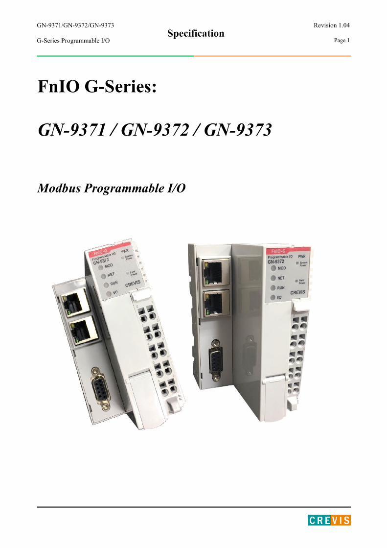
GN-9371/GN-9372/GN-9373 Specification
Revision 1.04
G-Series Programmable I/O Page 1
FnIO G-Series:
GN-9371 / GN-9372 / GN-9373
Modbus Programmable I/O

GN-9371/GN-9372/GN-9373 Specification
Revision 1.04
G-Series Programmable I/O Page 2
DOCUMENT CHANGE SUMMARY
REV. PAGES REMARKS DATE Editor
Preliminary 29 First Preliminary Apr 23, 2018 MK,Park
1.01 23,24 Modbus register change. Jun 21, 2018 MK,Park
1.02 23,24 Modbus special register change. Ju1 18, 2018 MK,Park
1.03 27 Adapter Setting Special Register change. Dec 20, 2018 MK,Park
1.04 26 Adapter Information Special Register change. Apr 26, 2019 MK,Park

GN-9371/GN-9372/GN-9373 Specification
Revision 1.04
G-Series Programmable I/O Page 3
Table of Contents Table of Contents ................................................................................................................................................ 3
1.ENVIRONMENT SPECIFICATION .............................................................................................................. 5
2.GN-9371/9372/9373 (G-SERIES PROGRAMMABLE I/O) .......................................................................... 6
2.1.GN-9371/9372/9373 Specification ........................................................................................................... 6
2.2.GN-9371/9372/9373 Ethernet connection specification .......................................................................... 8
2.3.GN-9371/9372/9373 Wiring Diagram ...................................................................................................... 9
2.4.GN-9371/9372/9373 LED Indicator ....................................................................................................... 10
2.4.1.LED Indicator .................................................................................................................................. 10
2.4.2.MOD (Module Status LED) ............................................................................................................ 10
2.4.3.NET (Network Status LED) ............................................................................................................ 10
2.4.4.RUN (PLC Run/Stop Status LED) .................................................................................................. 10
2.4.5.IOS LED (Expansion Module Status LED) ..................................................................................... 11
2.4.6.Field Power LED (Field Power Status LED) .................................................................................. 11
2.5.GN-9371/9372/9373 Electrical Interface ............................................................................................... 12
2.5.1.RJ-45 Socket .................................................................................................................................... 12
2.5.2.RS-232/RS-485 Port for MODBUS/RTU, Touch Pannel or IOGuide............................................. 12
2.5.3.Toggle Switch and Push Botton ....................................................................................................... 12
2.6.GN-9371/9372/9373 Web-Server ......................................................................................................... 13
3.MODBUS/RTU INTERFACE....................................................................................................................... 15
3.1.Surpported MODBUS Function Codes .................................................................................................. 15
3.1.1.1 (0x01) Read Coils ......................................................................................................................... 15
3.1.2.2 (0x02) Read Discrete Inputs ......................................................................................................... 16
3.1.3.3 (0x03) Read Holding Resgisters ................................................................................................... 16
3.1.4.4 (0x04) Read Input Resgisters ....................................................................................................... 17
3.1.5.5 (0x05) Write Single Coil ............................................................................................................... 17
3.1.6.6 (0x06) Write Single Register ........................................................................................................ 18
3.1.7.8 (0x08) Diagnostics ........................................................................................................................ 18
3.1.8.15 (0x0F) Write Multiple Coils ....................................................................................................... 21
3.1.9.16 (0x10) Write Multiple Resgisters................................................................................................ 21
3.1.10.23 (0x17) Read/Write Multiple Resgisters .................................................................................... 22
3.1.11.Error Response ............................................................................................................................... 23
3.2.MODBUS Special Register Map ............................................................................................................ 24
3.2.1.Adapter Resgister Mapping ............................................................................................................. 24

GN-9371/GN-9372/GN-9373 Specification
Revision 1.04
G-Series Programmable I/O Page 4
3.2.2.Adapter Identification Special Resgister (0x1000, 4096) ................................................................ 24
3.2.3.Adapter Information Special Register (0x1100, 4352) .................................................................... 25
3.2.4.Adapter Setting Special Register (0x1600, 5632) ........................................................................... 26
3.2.5.Expasion Slot Information Special Resister (0x2000, 8192) ........................................................... 27
3.3.Surpported MODBUS Function Codes .................................................................................................. 29

GN-9371/GN-9372/GN-9373 Specification
Revision 1.04
G-Series Programmable I/O Page 5
1. ENVIRONMENT SPECIFICATION
Environmental specification Operating Temperature -20℃~60℃ UL Temperature -20℃~60℃ Storage Temperature -40℃~85℃ Relative Humidity 5% ~ 90% non-condensing Mounting DIN rail Vibration Resistance EMC Resistance Burst/ESD IEC 60068-2-27 Installation Pos. / Protect. Class Based on IEC 60068-2-6
Sine Vibration 5 ~ 25Hz : 1.6mm 25 ~ 300Hz : 4g Sweep Rate : 1 Oct/min, 20 cycles Random Vibration 10 ~ 40Hz : 0.0125g²/Hz 40 ~ 100Hz : 0.0125 → 0.002g²/Hz 100 ~ 500Hz : 0.002g²/Hz 500 ~ 2000Hz : 0.002 → 1.3 x 10-⁴g²/Hz Test time : 1hours for each test
Product Certifications EN 61000-6-2 : 2005 EN 61000-6-4/A11 : 2011
Installation Pos. / Protect. Class Variable/IP20 Product Certifications FCC, KC, UL, RoHS2

GN-9371/GN-9372/GN-9373 Specification
Revision 1.04
G-Series Programmable I/O Page 6
2. GN-9371/9372/9373 (G-SERIES PROGRAMMABLE I/O)
2.1. GN-9371/9372/9373 Specification
Items Specification Programmable Specification Programming CoDeSys V3.5.11.3 Program Memory GN-9371 * 512 KBytes
GN-9372/9373 16 MBytes Data Memory GN-9371 96 KBytes IO Input: %IW0 ~%IW2047 (2048 words)
IO Output: %QW0 ~%QW2047 (2048 words) Memory: %MW0 ~ %MW8191 (8192 words) GN-9372/9373 16 MBytes
Non-Volatile Memory
GN-9371 4 KBytes (Retain : 2 KBytes, Flag : 2 KBytes) GN-9372/9373 32 KBytes (Retain : 16KBytes, Flag : 16 KBytes)
Run-Time System Multiple PLC Tasks Program Languages IEC 61131-3 (LD, IL, ST, FBD, SFC) OPC-Server GN-9371 Not supporting
GN-9372/9373 DA Online Change GN-9371 Not supporting
GN-9372/9373 Supporting Source Upload/Download
GN-9371 Not supporting GN-9372/9373 Supporting
File transmit GN-9371 Not supporting GN-9372/9373 Supporting
Breakpoint GN-9371 Not supporting GN-9372/9373 Supporting
Webvisualization GN-9371/9372 Not supporting GN-9373 Supporting
RTC GN-9371 Retain Time : < 15 day Accuracy : < 2min/month
GN-9372/9373 Retain Time : < 15 day Max. Task 10 Max. Cycle Task 10 Max. Status Task 10 Process Time GN-9371 1usec (90 Instructions)
GN-9372/9373 7usec (90 Instructions)

GN-9371/GN-9372/GN-9373 Specification
Revision 1.04
G-Series Programmable I/O Page 7
Interface Specification
Adapter Type Master & Slave Node (Modbus TCP, Modbus RTU) Max. Expansion Module 63 Slots Max. Data Size(Input+Output) Max 128Byte each slot Max. Nodes Limited by Ethernet Specification Baud rate 10/100Mbps, Auto-negotiation, Full Duplex Ethernet Interface RJ-45 socket * 2pcs Ethernet Protocol** Modbus/TCP, Modbus/UDP, SNTP
HTTP (Webvisualization***, Web-Server), DHCP/BOOTP, OPC-server Max. Socket 24 (UDP: 8, TCP: 16, TCP_LISTEN: 10) Serial Interface RS232/RS485 2port (supporting Touch Pannel) Serial Protocol Modbus/RTU / Baud Rate : 2400~115200 bps (Default: 115200 bps) Indicator 6 LEDs
1 Green/Red, Module Status (MOD) 1 Green/Red, Network Status (NET) 1 Green/Red, PLC Run/Stop Status (RUN) 1 Green/Red, Expansion I/O Module Status (IOS) 1 Green, System Power Status 1 Green, Field Power Status
General specification
System Power Supply voltage : 24Vdc nominal Supply voltage range : 15~32Vdc Protection : Output current limit (Min. 1.5A) / Reverse polarity protection
Power Dissipation 110mA typical @ 24Vdc
Current for I/O Module 1.5A @ 5Vdc
Isolation System power to internal logic : Non-isolation System power I/O driver : Isolation
Field Power Supply voltage : 24Vdc typical (Max. 32Vdc) * Field Power Range is different depending on IO Module series.

GN-9371/GN-9372/GN-9373 Specification
Revision 1.04
G-Series Programmable I/O Page 8
Refer to IO Module`s Specification.
Max. Current Field Power Contact DC 10A Max
Weight <167g
Module Size 54mm x 99mm x 70mm
Environment Condition Refer to ‘1. Environment Specification’
* GN-9371 is an economic version derived from GN-9372.
*** Webvisualization cannot be supported in Internet Explorer.
2.2. GN-9371/9372/9373 Ethernet connection specification
Function* Model Max. number of concurrent communications
Webvisualization GN-9373 only
One for each functions are available at the same time ARTI (OPC-server) GN-9372/73
CoDeSys link GN-9371/72/73
Network-variable GN-9371/72/73
Modbus/TCP Master GN-9371/72/73 5 Modbus/TCP Slaves can be connected
Modbus/TCP Slave GN-9371/72/73 16 Modbus/TCP Masters can be connected
Web-server GN-9371/72/73 16 clients can be opened
* While using these functions,16 sockets are available at the same time.

GN-9371/GN-9372/GN-9373 Specification
Revision 1.04
G-Series Programmable I/O Page 9
2.3. GN-9371/9372/9373 Wiring Diagram
Pin No. Signal Description Signal Description Pin No.
0 System Power, 24V System Power, Ground 1
2 System Power, 24V System Power, Ground 3
4 F.G F.G 5
6 Field Power, Ground Field Power 0V, Ground 7
8 Field Power, 24V Field Power, 24V 9
* Warning: The system power must not be connected with field power. Use seperate voltage supplies.

GN-9371/GN-9372/GN-9373 Specification
Revision 1.04
G-Series Programmable I/O Page 10
2.4. GN-9371/9372/9373 LED Indicator 2.4.1. LED Indicator
2.4.2. MOD (Module Status LED)
Status LED is To indicate
Not Powered OFF Power is not supplied to the unit.
Normal, Operational Green The unit is operating in normal condition.
Devicce in Standby Blinking Green The EEPROM parameter is not initialized yet. Serial Number is zero value (0x00000000)
IAP Mode Toggling Green & Red IAP Mode : Availble for firmware download using FireFox.
Unrecoverable Fault Red The unit has occurred unrecoverable fault in self-testing. - Firmware fault
* The IP Address to access IAP web-server during IAP Mode: 192.168.100.10 (Recommended to use FireFox)
2.4.3. NET (Network Status LED)
Status LED is To indicate
Off-line OFF Network Offline.
On-line (Connect) Green On-line Mode and network is connected.
Error Red Network Error
Diagnorstic Blinking Red Diagnostic Mode
*Blinking Green MOD & NET LED: Bootp/DHCP is requesting for new IP address.
(You can change the IP setting mode. Please refer to specification.)
2.4.4. RUN (PLC Run/Stop Status LED)
Status LED is To indicate
Not programmed OFF The unit is not programmed or not powered.
Run Green PLC Run
Stop Blinking Green PLC Stop
Program Error Blinking Red PLC program error

GN-9371/GN-9372/GN-9373 Specification
Revision 1.04
G-Series Programmable I/O Page 11
2.4.5. IOS LED (Expansion Module Status LED)
Status LED is To indicate
Not Powered No Expansion Module
OFF Device has no expansion module or may not be powered.
On-line, Do not Exchanging I/O
Blinking Green
I/O Communication is normal but does not exchanging I/O data. (Passed the expantion module configuration)
Connection, Run Exchanging I/O
Green Exchanging I/O data.
Connection Fault during Exchanging I/O
Blinking Red
One or more expansion module occurred in fault state. - Changed expansion module configuration. - Communication failure. - Overflowed Input/Output size.
Expansion Configuration Failed
Red Failed to initalize expansion module. - Detect invalid expansion module ID. - Too many expansion module. - Initial protocol failure. - Mismatch vendor code between adapter and expension module.
2.4.6. Field Power LED (Field Power Status LED)
Status LED is To indicate
Not supplied field power OFF Not supplied 24Vdc field power.
Supplied field power Green Supplied 24Vdc field power.

GN-9371/GN-9372/GN-9373 Specification
Revision 1.04
G-Series Programmable I/O Page 12
#2 TXD
#3 RXD
#6 D+
#8 D-
#5 GND
2.5. GN-9371/9372/9373 Electrical Interface 2.5.1. RJ-45 Socket
Shielded RJ-45 Socket
2.5.2. RS-232/RS-485 Port for MODBUS/RTU, Touch Pannel or IOGuide
2.5.3. Toggle Switch and Push Botton
D-Sub 9Pin Pin# Signal Name Description
1 - 2 TXD RS232 TXD 3 RXD RS232 RXD 4 - 5 GND RS232 GND 6 D+ RS485 D+ 7 - 8 D- RS485 D- 9 -
RJ-45 Signal Name Description 1 TD+ Transmit + 2 TD- Transmit - 3 RD+ Receive + 4 - 5 - 6 RD- Receive - 7 - 8 -
Case Shield

GN-9371/GN-9372/GN-9373 Specification
Revision 1.04
G-Series Programmable I/O Page 13
Toggle Switch Status Module is Description
UP RUN PLC Run
DOWN STOP PLC Stop
Push Botton Module is Description Push and detach Reset PLC Reset and Stop
Push for 5sec and Power Reset PLC Reset Erase PLC user program and Retain memory
Push for 20sec and Power Reset Factory Reset Erase PLC user program and PLC parameter reset
Push hold and Power Reset IAP mode Firmware download via FireFox.
2.6. GN-9371/9372/9373 Web-Server * Web-Server Address : http://IP/setup.htm (http://192.168.100.25/setup.htm)
- Showing the expension modules that attatched to PIO

GN-9371/GN-9372/GN-9373 Specification
Revision 1.04
G-Series Programmable I/O Page 14
- Showing CoDeSys PLC programming information and RTC time setting. RTC time can be chnageable in this page.

GN-9371/GN-9372/GN-9373 Specification
Revision 1.04
G-Series Programmable I/O Page 15
- Nework setting can be changeable in this page.
3. MODBUS/RTU INTERFACE
3.1. Surpported MODBUS Function Codes
Function Code Function Description
1(0x01) Read Coils Read output bit
2(0x02) Read Discrete Inputs Read input bit
3(0x03) Read Holding Registers Read output word
4(0x04) Read Input Registers Read input word
5(0x05) Write Single Coil Write one bit output
6(0x06) Write Single Register Write one word output
8(0x08) Diagnostics Read diagnostic register
15(0x0F) Write Multiple Coils Write a number of output bits
16(0x10) Write Multiple registers Write a number of output words
23(0x17) Read/Write Multiple registers Read a number of input words /Write a number of output words

GN-9371/GN-9372/GN-9373 Specification
Revision 1.04
G-Series Programmable I/O Page 16
- Refer to MODBUS APPLICATION PROTOCOL SPECIFICATION V1.1a
3.1.1. 1 (0x01) Read Coils
This function code is used to read from 1 to 2000 contiguous status of coils in a remote device. The Request PDU specifies the starting address, i.e. the address of the first coil specified, and the number of coils. In the PDU Coils are addressed starting at zero. Therefore coils numbered 1-16 are addressed as 0-15. The coils in the response message are packed as one coil per bit of the data field. Status is indicated as 1= ON and 0= OFF.
• Request
Field name Example Function Code 0x01 Starting Address Hi 0x10 Starting Address Lo 0x00 Quantity of Outputs Hi 0x00 Quantity of Outputs Lo 0x0A
• Response
Field name Example Function Code 0x01 Byte Count 0x02 Output Status 0x55 Output Status 0x02
- In case of address 0x1015~0x1000 output bit value: 10101010_01010101.
3.1.2. 2 (0x02) Read Discrete Inputs
This function code is used to read from 1 to 2000 contiguous status of discrete inputs in a remote device. The Request PDU specifies the starting address, i.e. the address of the first input specified, and the number of inputs. In the PDU Discrete Inputs are addressed starting at zero. Therefore Discrete inputs numbered 1-16 are addressed as 0-15.
The discrete inputs in the response message are packed as one input per bit of the data field.
Status is indicated as 1= ON; 0= OFF.
• Request
Field name Example Function Code 0x02 Starting Address Hi 0x00 Starting Address Lo 0x00 Quantity of Inputs Hi 0x00 Quantity of Inputs Lo 0x0A
• Response
Field name Example Function Code 0x02 Byte Count 0x02 Input Status 0x80 Input Status 0x00

GN-9371/GN-9372/GN-9373 Specification
Revision 1.04
G-Series Programmable I/O Page 17
- In case of address 0x0015~0x0000 input bit value: 00000000_10000000.
3.1.3. 3 (0x03) Read Holding Resgisters
This function code is used to read the contents of a contiguous block of holding registers in a remote device. The Request PDU specifies the starting register address and the number of registers.
The register data in the response message are packed as two bytes per register, with the binary contents right justified within each byte. For each register, the first byte contains the high order bits and the second contains the low order bits.
• Request
Field name Example Function Code 0x03 Starting Address Hi 0x08 Starting Address Lo 0x00 Quantity of Register Hi 0x00 Quantity of Register Lo 0x02
• Response
Field name Example Function Code 0x03 Byte Count 0x04 Output Register#0 Hi 0x11 Output Register#0 Lo 0x22 Output Register#1 Hi 0x33 Output Register#1 Lo 0x44
- In case of address 0x0800, 0x0801 output register value: 0x1122, 0x3344.
3.1.4. 4 (0x04) Read Input Resgisters
This function code is used to read from 1 to approx. 125 contiguous input registers in a remote device. The Request PDU specifies the starting register address and the number of registers. The register data in the response message are packed as two bytes per register, with the binary contents right justified within each byte. For each register, the first byte contains the high order bits and the second contains the low order bits.
• Request
Field name Example Function Code 0x04 Starting Address Hi 0x00 Starting Address Lo 0x00 Quantity of Register Hi 0x00 Quantity of Register Lo 0x02
• Response
Field name Example Function Code 0x03 Byte Count 0x04 Input Register#0 Hi 0x00 Input Register#0 Lo 0x80 Input Register#1 Hi 0x00

GN-9371/GN-9372/GN-9373 Specification
Revision 1.04
G-Series Programmable I/O Page 18
Input Register#1 Lo 0x00
- In case of address 0x0000, 0x0001 input register value: 0x0080, 0x0000.
3.1.5. 5 (0x05) Write Single Coil
This function code is used to write a single output to either ON or OFF in a remote device. The requested ON/OFF state is specified by a constant in the request data field. A value of FF 00 hex requests the output to be ON. A value of 00 00 requests it to be OFF. All other values are illegal and will not affect the output.
• Request
Field name Example Function Code 0x05 Output Address Hi 0x10 Output Address Lo 0x01 Output Value Hi 0xFF Output Value Lo 0x00
• Response
Field name Example Function Code 0x05 Output Address Hi 0x10 Output Address Lo 0x01 Output Value Hi 0xFF Output Value Lo 0x00
- Output bit of address 0x1001 turns ON.
3.1.6. 6 (0x06) Write Single Register
This function code is used to write a single holding register in a remote device. Therefore register numbered 1 is addressed as 0. The normal response is an echo of the request, returned after the register contents have been written.
• Request
Field name Example Function Code 0x06 Register Address Hi 0x08 Register Address Lo 0x00 Register Value Hi 0x11 Register Value Lo 0x22
• Response
Field name Example Function Code 0x06 Register Address Hi 0x08 Register Address Lo 0x00 Register Value Hi 0x11 Register Value Lo 0x22
- In case of address 0x0800 output register value: 0x0000 changes to 0x1122.

GN-9371/GN-9372/GN-9373 Specification
Revision 1.04
G-Series Programmable I/O Page 19
3.1.7. 8 (0x08) Diagnostics
MODBUS function code 08 provides a series of tests for checking the communication system between a client ( Master) device and a server ( Slave), or for checking various internal error conditions within a server.
The function uses a two–byte sub-function code field in the query to define the type of test to be performed. The server echoes both the function code and sub-function code in a normal response. Some of the diagnostics cause data to be returned from the remote device in the data field of a normal response.
• Request
Field name Example Function Code 0x08 Sub-Function Hi 0x00 Sub-Function Lo 0x00 Data Hi 0x11 Data Lo 0x22
• Response
Field name Example Function Code 0x08 Sub-Function Hi 0x00 Sub-Function Lo 0x00 Data Hi 0x11 Data Lo 0x22
Sub-function 0x0000(0) Return Query Data
The data passed in the request data field is to be returned (looped back) in the response.
The entire response message should be identical to the request.
Sub-function Data Field (Request) Data Field (Response) Description 0x0000(0) Any Echo Request Data
Sub-function 0x0001(1) Restart Communications Option
The remote device could be initialized and restarted, and all of its communications event counters are cleared.
Especially, data field 0x55AA make the remote device to restart with factory default setup of EEPROM.
Sub-function Data Field (Request) Data Field (Response) Description
0x0001(1) 0x0000 or 0xFF00 Echo Request Data Reset
0x0001(1) 0x55AA Echo Request Data Reset with Default Setting 1)

GN-9371/GN-9372/GN-9373 Specification
Revision 1.04
G-Series Programmable I/O Page 20
0x0001(1) 0x55AA+0xAB7B+Sumcheck 4) Echo Request Data Reset with Factory default 2)
0x0001(1) 0x55AA+0xAA55+Sumcheck 4) Echo Request Data Reset with Factory default 3)
1),2),3) All expansion slot configuration parameters are cleared.
2),3) IP Address, Subnet Mask Address, Gateway Address, RS232/485 setting, and Bootp/DHCP mode will be the factory defaults value.
3) Mac Address will be the factory default value.
4) Refer to 3.2.2 for Sumcheck (0x1006)
Sub-function 0x000A(10) Clear Counters and Diagnostic Register
The goal is to clear all counters and the diagnostic register. Counters are also cleared upon power–up.
Sub-function Data Field (Request) Data Field (Response) Description 0x000A(10) 0x0000 Echo Request Data
Sub-function 0x000B(11) Return Bus Message Count
The response data field returns the quantity of messages that the remote device has detected on the communications system since its last restart, clear counters operation, or power–up.
Sub-function Data Field (Request) Data Field (Response) Description 0x000B(11) 0x0000 Total Message Count
Sub-function 0x000D(13) Return Bus Exception Error Count
The response data field returns the quantity of MODBUS exception responses returned by the remote device since its last restart, clear counters operation, or power–up.
Exception responses are described and listed in section 3.2.11.
Sub-function Data Field (Request) Data Field (Response) Description 0x000D(13) 0x0000 Exception Error Count
Sub-function 0x000E(14) Return Slave Message Count
The response data field returns the quantity of messages addressed to the remote device, or broadcast, that the remote device has processed since its last restart, clear counters operation, or power–up.
Sub-function Data Field (Request) Data Field (Response) Description 0x000E(14) 0x0000 Slave Message Count
Sub-function 0x000F(15) Return Slave No Response Count

GN-9371/GN-9372/GN-9373 Specification
Revision 1.04
G-Series Programmable I/O Page 21
The response data field returns the quantity of messages addressed to the remote device for which it has returned no response (neither a normal response nor an exception response), since its last restart, clear counters operation, or power–up.
Sub-function Data Field (Request) Data Field (Response) Description 0x000F(15) 0x0000 Slave No Response Count
Sub-function 0x0064(100) Return Slave ModBus, Expansion Status
The response data field returns the status of ModBus and expansion addressed to the remote device.
This status values are identical with status 1word of input process image.
Sub-function Data Field (Request) Data Field (Response) Description 0x0064(100) 0x0000 ModBus, G-Bus Status Same as status 1word

GN-9371/GN-9372/GN-9373 Specification
Revision 1.04
G-Series Programmable I/O Page 22
3.1.8. 15 (0x0F) Write Multiple Coils
This function code is used to force each coil in a sequence of coils to either ON or OFF in a remote device. The Request PDU specifies the coil references to be forced. Coils are addressed starting at zero. A logical '1' in a bit position of the field requests the corresponding output to be ON. A logical '0' requests it to be OFF.
The normal response returns the function code, starting address, and quantity of coils forced.
• Request
Field name Example Function Code 0x0F Starting Address Hi 0x10 Starting Address Lo 0x00 Quantity of Outputs Hi 0x00 Quantity of Outputs Lo 0x0A Byte Count 0x02 Output Value#0 0x55 Output Value#1 0x01
• Response
Field name Example Function Code 0x0F Starting Address Hi 0x10 Starting Address Lo 0x00 Quantity of Outputs Hi 0x00 Quantity of Outputs Lo 0x0A
– In case of address 0x1015~0x1000 output bit value: 00000000_00000000 changes to 00000001_01010101.
3.1.9. 16 (0x10) Write Multiple Resgisters
This function code is used to write a block of contiguous registers (1 to approx. 120 registers) in a remote device.
The requested written values are specified in the request data field. Data is packed as two bytes per register.
The normal response returns the function code, starting address, and quantity of registers written.
• Request
Field name Example Function Code 0x0F Starting Address Hi 0x10 Starting Address Lo 0x08 Quantity of Registers Hi 0x00 Quantity of Registers Lo 0x02 Byte Count 0x04 Register Value#0 Hi 0x11 Register Value#0 Lo 0x22 Register Value#1 Hi 0x33 Register Value#1 Lo 0x44

GN-9371/GN-9372/GN-9373 Specification
Revision 1.04
G-Series Programmable I/O Page 23
• Response
Field name Example Function Code 0x0F Starting Address Hi 0x10 Starting Address Lo 0x08 Quantity of Registers Hi 0x00 Quantity of Registers Lo 0x02
.- In case of address 0x0800, 0x0801 output register value: 0x0000, 0x0000 changes to 0x1122, 0x3344.
3.1.10. 23 (0x17) Read/Write Multiple Resgisters
This function code performs a combination of one read operation and one write operation in a single MODBUS transaction. The write operation is performed before the read. The request specifies the starting address and number of holding registers to be read as well as the starting address, number of holding registers, and the data to be written. The byte count specifies the number of bytes to follow in the write data field.
The normal response contains the data from the group of registers that were read. The byte count field specifies the quantity of bytes to follow in the read data field.
• Request
Field name Example Function Code 0x17 Read Starting Address Hi 0x08 Read Starting Address Lo 0x00 Quantity of Read Hi 0x00 Quantity of Read Lo 0x02 Write Starting Address Hi 0x08 Write Starting Address Lo 0x00 Quantity of Write Hi 0x00 Quantity of Write Lo 0x02 Byte Count 0x04 Write Reg. Value#0 Hi 0x11 Write Reg. Value#0 Lo 0x22 Write Reg. Value#1 Hi 0x33 Write Reg. Value#1 Lo 0x44
• Response
Field name Example Function Code 0x17 Byte Count 0x04 Read Reg. Value#0 Hi 0x11 Read Reg. Value#0 Lo 0x22 Read Reg. Value#1 Hi 0x33 Read Reg. Value#1 Lo 0x44
- In case of address 0x0800, 0x0801 output register value: 0x0000, 0x0000 changes to 0x1122, 0x3344.
GN-9371/GN-9372/GN-9373 Specification
Revision 1.04
G-Series Programmable I/O Page 24
3.1.11. Error Response
In an exception response, the server sets the MSB of the function code to 1. This makes the function code value in an exception response exactly 80 hexadecimal higher than the value would be for a normal response.
• Exception Response Example
Field name Example Function Code 0x81 Exception Code 0x02
• Exception Codes
Exception Code
Name Description
01 Illegal Function The function code received in the query is not an allowable action for the server (or slave).
02 Illegal Data Address The data address received in the query is not an allowable address for the server (or slave).
03 Illegal Data Value A value contained in the query data field is not an allowable value for server (or slave).
04 Slave Device Failure An unrecoverable error occurred while the server (or slave) was attempting to perform the requested action.
06 Slave Device Busy Specialized use in conjunction with programming commands. The server (or slave) is engaged in processing a long–duration program command. The client (or master) should retransmit the message later when the server (or slave) is free.
GN-9371/GN-9372/GN-9373 Specification
Revision 1.04
G-Series Programmable I/O Page 25
3.2. MODBUS Special Register Map The special register map can be accessed by function code 3, 4, 6 and 16. Also the special register map must be accessed by read/write of every each address (one address).
3.2.1. Adapter Resgister Mapping
Address IEC Address Contents Remarks 0x0000~0x07FF %IW0~%IW2047 2048 words Input and Internal memory (Area is write-protected) 0x0800~0x0FFF %QW0~%QW2047 2048 words Output and Internal memory (Area is write-enabled) 0x1000~0x1FFF - Special Function Register (PIO Information) 0x2000~0x2FFF - Special Function Register (Slot Information) 0x4000~0x5FFF %MW0~%MW8191 8192 words Internal memory (Area is write-enabled)
3.2.2. Adapter Identification Special Resgister (0x1000, 4096)
Address Access Type, Size Description 0x1000(4096) Read 1word Vendor ID = 0x02E5(741), Crevis. Co., Ltd. 0x1001(4097) Read 1word Device type = 0x000C, Network Adapter 0x1002(4098) Read 1word Product Code = 0x9100(GN-9371) / 0x9110(GN-9372)
/ 0x9120(GN-9373) 0x1003(4099) Read 1word Firmware revision, if 0x0101, revision 1.001 0x1005(4101) Read String
upto 34bytes
Product name string First 1word is length of valid character string Example) response as following “00 1D 52 4E 2D 39 32 32 32 2C 50 72 6F 66 69 62 75 73 20 41 64 61 70 74 65 72 2C 52 42 55 53 00 00 000” Valid character size = 0x0017 =29 characters "GN-9372(PIO)"
0x1006(4102) Read 1word Sum check of EEPROM 0x1010(4112) Read 2words Firmware release date 0x101E(4126)
Read 15words Composite Id of following address 0xA8C0(Lo_IP Addr),0x3264(Hi_IP Addr),0xFFFF(Lo_NetMask), 0x00FF(Hi_NetMask),0xA8C0(GateWay),0xFE64(GateWay), 0x1400(MacAddr),0x00F7(MacAddr),0xBA83(MacAddr), 0x02E5(VendorCode),0x000C(DeviceType),0x9120(ProductCode), 0x0200(FW_Rev),0x0420(FW_ReleasData),0x2018(FW_ReleasYear)
- String Type consists of valid string length (first 1word) and array of characters

GN-9371/GN-9372/GN-9373 Specification
Revision 1.04
G-Series Programmable I/O Page 26
3.2.3. Adapter Information Special Register (0x1100, 4352)
Address Access Type, Size Description 0x1102(4354) Read 1word Start address of input image word register. =0x0000 0x1103(4355) Read 1word Start address of output image word register. =0x0800 0x1104(4356) Read 1word Size of input image word register. 0x1105(4357) Read 1word Size of output image word register. 0x1106(4358) Read 1word Start address of input image bit. = 0x0000 0x1107(4359) Read 1word Start address of output image bit. =0x1000 0x1108(4360) Read 1word Size of input image bit. 0x1109(4361) Read 1word Size of output image bit. 0x110D(4365) Read 1word Field Power On/OFF, Run/Stop Switch, Reset Switch
*Field Power On : 0x8010 / Field Power Off : 0x0000 *Stop : 0x0000 / Run : 0x0001 / Reset Switch : 0x0002 ex) 0x8013 : Field Power On + Run + Reset Switch ON
0x110E(4366) Read upto 63words
Expansion slot’s GT-number If the PIO is connected with GT-222F and GT-123F, then 0x222F 0x123F
0x1110(4368) Read 1word Number of expansion slot. 0x1113(4371) Read upto
63words Expansion slot Module Id. Refer to Appendix A.1 Product List. First 1word is adapter’s module id.
0x111E(4382) Read 1word Reserved. Adapter IO identification vendor code.

GN-9371/GN-9372/GN-9373 Specification
Revision 1.04
G-Series Programmable I/O Page 27
3.2.4. Adapter Setting Special Register (0x1600, 5632)
Address Access Type, Size Description 0x1600(5632) Read 2words IP Address. (ex : A8C0 6464 = 192.168.100.100) 0x1602(5634) Read 2words Subnet Mask. (ex : FFFF 0000 = 255.255.0.0) 0x1604(5636) Read 2words Gate way. (ex : A8C0 0100 = 192.168.0.1) 0x1606(5638) Read/Write 1word RS-232C Baudrate. (2400bps~115200bps)
- 0 : 115200 (default) - 1 : 2400 - 2 : 4800 - 3 : 9600 - 4 : 19200 - 5 : 38400 - 6 : 57600 - 7 : 115200
0x1607(5639) Read/Write 1word *RS-232C Setting. - 1 nibble : Data bit(0 : 8bit(default), 1 : 9bit) - 2 nibble : Stop bit(0 : 1bit(default), 1 : 2bit) - 3 nibble : Parity bit(0 : none(default), 1: odd, 2 : even) - 4 nibble : Reserve
0x1608(5640) Read/Write 1word RS-485 Baudrate. (2400bps~115200bps) - 0 : 115200 (default) - 1 : 2400 - 2 : 4800 - 3 : 9600 - 4 : 19200 - 5 : 38400 - 6 : 57600 - 7 : 115200
0x1609(5641) Read/Write 1word RS-485 Setting. - 1 nibble : Data bit(0 : 8bit(default), 1 : 9bit) - 2 nibble : Stop bit(0 : 1bit(default), 1 : 2bit) - 3 nibble : Parity bit(0 : none(default), 1: odd, 2 : even) - 4 nibble : Reserve
0x160A(5642) Read/Write 1word **Modbus Station. - High 1byte : Station No. of RS-232C (default : 1) - Low 1byte : Station No. of RS-485 (default : 1)
0x160B(5643) Read/Write 1word IP Setting Method. - BootP/DHCP disable: 0x0000 - BootP : 0x8000 (default) - DHCP : 0x8001
0x1610(5648) Read 3words Mac Address (ex : 1400 00F7 0101 = 00.14.F7.00.01.01) 0x1614(5652)* Read 1word Serial connection Method
- 0x0000 : Crevis Modbus/RTU (default) - 0x8000 : RS232 Enable for CoDeSys Function block / RTU Master - 0x8001 : RS485 Enable for CoDeSys Function block / RTU Master - 0x8002 : RS232/RS485 Enable at the same time for CoDeSys Function block / RTU Master
0x1620(5664) Read/Write 4words RTC - 1 word : 00ss (ss : sec) - 2 word : hhmm (hh : hour, mm : min) - 3 word : mmdd (mm : month, dd : day) - 4 word : yyyy (yyyy : year) (ex : 0010 0F28 0317 07E0 = 2016 - 03.23 - 15:40 - 16)

GN-9371/GN-9372/GN-9373 Specification
Revision 1.04
G-Series Programmable I/O Page 28
*RS-232C/485 Setting : This description for 0x1607/0x1609 register with bit.
**Modbus Station : This description for 0x160A register with bit.
3.2.5. Expasion Slot Information Special Resister (0x2000, 8192)
Each expansion slot has 0x40(64) address offset and same information structure.
Slot#1 0x2000(8192)~0x201F(8223) Slot#2 0x2020(8224)~0x203F(8255) Slot#3 0x2040(8256)~0x205F(8287) Slot#4 0x2060(8288)~0x207F(8319) Slot#5 0x2080(8320)~0x209F(8351) Slot#6 0x20A0(8352)~0x20BF(8383) Slot#7 0x20C0(8384)~0x20DF(8415) Slot#8 0x20E0(8416)~0x20FF(8447) Slot#9 0x2100(8448)~0x211F(8479) Slot#10 0x2120(8480)~0x213F(8511) Slot#11 0x2140(8512)~0x215F(8543) Slot#12 0x2160(8544)~0x217F(8575) Slot#13 0x2180(8576)~0x219F(8607) Slot#14 0x21A0(8608)~0x21BF(8639) Slot#15 0x21C0(8640)~0x21DF(8671) Slot#16 0x21E0(8672)~0x21FF(8703) Slot#17 0x2200(8704)~0x221F(8735) Slot#18 0x2220(8736)~0x223F(8767) Slot#19 0x2240(8768)~0x225F(8799) Slot#20 0x2260(8800)~0x227F(8831) Slot#21 0x2280(8832)~0x229F(8863) Slot#22 0x22A0(8864)~0x22BF(8895) Slot#23 0x22C0(8896)~0x22DF(8927) Slot#24 0x22E0(8928)~0x22FF(8959) Slot#25 0x2300(8960)~0x231F(8991) Slot#26 0x2320(8992)~0x233F(9023) Slot#27 0x2340(9024)~0x235F(9055) Slot#28 0x2360(9056)~0x237F(9087) Slot#29 0x2380(9088)~0x239F(9119) Slot#30 0x23A0(9120)~0x23BF(9151) Slot#31 0x23C0(9152)~0x23DF(9183) Slot#32 0x23E0(9184)~0x23FF(9215) Slot#33 0x2400(9216)~0x241F(9247) Slot#34 0x2420(9248)~0x243F(9279) Slot#35 0x2440(9280)~0x245F(9311) Slot#36 0x2460(9312)~0x247F(9343) Slot#37 0x2480(9344)~0x249F(9375) Slot#38 0x24A0(9376)~0x24BF(9407) Slot#39 0x24C0(9408)~0x24DF(9439) Slot#40 0x24E0(9440)~0x24FF(9471) Slot#41 0x2500(9472)~0x251F(9503) Slot#42 0x2520(9504)~0x253F(9535) Slot#43 0x2540(9536)~0x255F(9567) Slot#44 0x2560(9568)~0x257F(9599) Slot#45 0x2580(9600)~0x259F(9631) Slot#46 0x25A0(9632)~0x25BF(9663) Slot#47 0x25C0(9664)~0x25DF(9695) Slot#48 0x25E0(9696)~0x25FF(9727) Slot#49 0x2600(9728)~0x261F(9759) Slot#50 0x2620(9760)~0x263F(9791) Slot#51 0x2640(9792)~0x265F(9823) Slot#52 0x2660(9824)~0x267F(9855) Slot#53 0x2680(9856)~0x269F(9887) Slot#54 0x26A0(9888)~0x26BF(9919) Slot#55 0x26C0(9920)~0x26DF(9951) Slot#56 0x26E0(9952)~0x26FF(9983) Slot#57 0x2700(9984)~0x271F(10015) Slot#58 0x2720(10016)~0x273F(10047) Slot#59 0x2740(10048)~0x275F(10079) Slot#60 0x2760(10080)~0x277F(10111) Slot#61 0x2780(10112)~0x279F(10143) Slot#62 0x27A0(10144)~0x27BF(10175)

GN-9371/GN-9372/GN-9373 Specification
Revision 1.04
G-Series Programmable I/O Page 29
Slot#63 0x27C0(10176)~0x27DF(10207)
Address Offset
Expansion Slot#1
Expansion Slot#2
Expansion Slot#3
Expansion Slot#4
…….. Expansion Slot#63
+ 0x00(+0) 0x2000(8192) 0x2020(8224) 0x2040(8256) 0x2060(8288) ……. 0x27C0(10176) + 0x01(+1) 0x2001(8193) 0x2021(8225) 0x2041(8257) 0x2061(8289) ……. 0x27C1(10177) + 0x02(+2) 0x2002(8194) 0x2022(8226) 0x2042(8258) 0x2062(8290) ……. 0x27C2(10178) + 0x03(+3) 0x2003(8195) 0x2023(8227) 0x2043(8259) 0x2063(8291) ……. 0x27C3(10179) + 0x04(+4) 0x2004(8196) 0x2024(8228) 0x2044(8260) 0x2064(8292) ……. 0x27C4(10180) + 0x05(+5) 0x2005(8197) 0x2025(8229) 0x2045(8261) 0x2065(8293) ……. 0x27C5(10181) + 0x06(+6) 0x2006(8198) 0x2026(8230) 0x2046(8262) 0x2066(8294) ……. 0x27C6(10182) + 0x07(+7) 0x2007(8199) 0x2027(8231) 0x2047(8263) 0x2067(8295) ……. 0x27C7(10183) + 0x08(+8) 0x2008(8200) 0x2028(8232) 0x2048(8264) 0x2068(8296) ……. 0x27C8(10184) + 0x09(+9) 0x2009(8201) 0x2029(8233) 0x2049(8265) 0x2069(8297) ……. 0x27C9(10185)
+ 0x0A(+10) 0x200A(8202) 0x202A(8234) 0x204A(8266) 0x206A(8298) ……. 0x27CA(10186) + 0x0B(+11) 0x200B(8203) 0x202B(8235) 0x204B(8267) 0x206B(8299) ……. 0x27CB(10187) + 0x0C(+12) 0x200C(8204) 0x202C(8236) 0x204C(8268) 0x206C(8300) ……. 0x27CC(10188) + 0x0D(+13) 0x200D(8205) 0x202D(8237) 0x204D(8269) 0x206D(8301) ……. 0x27CD(10189) + 0x0E(+14) 0x200E(8206) 0x202E(8238) 0x204E(8270) 0x206E(8302) ……. 0x27CE(10190) + 0x0F(+15) 0x200F(8207) 0x202F(8239) 0x204F(8271) 0x206F(8303) ……. 0x27CF(10191) + 0x10(+16) 0x2010(8208) 0x2030(8240) 0x2050(8272) 0x2070(8304) ……. 0x27D0(10192) + 0x11(+17) 0x2011(8209) 0x2031(8241) 0x2051(8273) 0x2071(8305) ……. 0x27D1(10193) + 0x12(+18) 0x2012(8210) 0x2032(8242) 0x2052(8274) 0x2072(8306) ……. 0x27D2(10194) + 0x13(+19) 0x2013(8211) 0x2033(8243) 0x2053(8275) 0x2073(8307) ……. 0x27D3(10195) + 0x14(+20) 0x2014(8212) 0x2034(8244) 0x2054(8276) 0x2074(8308) ……. 0x27D4(10196) + 0x15(+21) 0x2015(8213) 0x2035(8245) 0x2055(8277) 0x2075(8309) ……. 0x27D5(10197) + 0x16(+22) 0x2016(8214) 0x2036(8246) 0x2056(8278) 0x2076(8310) ……. 0x27D6(10198) + 0x17(+23) 0x2017(8215) 0x2037(8247) 0x2057(8279) 0x2077(8311) ……. 0x27D7(10199) + 0x18(+24) 0x2018(8216) 0x2038(8248) 0x2058(8280) 0x2078(8312) ……. 0x27D8(10200) + 0x19(+25) 0x2018(8217) 0x2038(8249) 0x2058(8281) 0x2078(8313) ……. 0x27D9(10201) + 0x1A(+26) 0x201A(8218) 0x203A(8250) 0x205A(8282) 0x207A(8314) ……. 0x27DA(10202) + 0x1B(+27) 0x201B(8219) 0x203B(8251) 0x205B(8283) 0x207B(8315) ……. 0x27DB(10203) + 0x1C(+28) 0x201C(8220) 0x203C(8252) 0x205C(8284) 0x207C(8316) ……. 0x27DC(10204) + 0x1D(+29) 0x201D(8221) 0x203D(8253) 0x205D(8285) 0x207D(8317) ……. 0x27DD(10205) + 0x1E(+30) 0x201E(8222) 0x203E(8254) 0x205E(8286) 0x207E(8318) ……. 0x27DE(10206) + 0x1F(+31) 0x201F(8223) 0x203F(8255) 0x205F(8287) 0x207F(8319) ……. 0x27DF(10207)
Address Offset Access Type, Size Description + 0x00(+0) Read 1 word Slot module id. + 0x02(+2) ** Read 1 word Input start register address of input image word this slot. + 0x03(+3) ** Read 1 word Input word’s bit offset of input image word this slot. + 0x04(+4) ** Read 1 word Output start register address of output image word this slot. + 0x05(+5) ** Read 1 word Output word’s bit offset of output image word this slot. + 0x06(+6) ** Read 1 word Input bit start address of input image bit this slot. + 0x07(+7) ** Read 1 word Output bit start address of output image bit this slot. + 0x08(+8) ** Read 1 word Size of input bit this slot + 0x09(+9) ** Read 1 word Size of output bit this slot + 0x0A(+10)** Read n word Read input data this slot + 0x0B(+11)** Read/Write n word Read/write output data this slot + 0x0E(+14) Read 1 word GT-number, if GT-22CA, returns 0x22CA

GN-9371/GN-9372/GN-9373 Specification
Revision 1.04
G-Series Programmable I/O Page 30
+ 0x0F(+15) Read String upto 72bytes
First 1word is length of valid character string. If GT-22CA, returns “00 1C 47 54 2D 32 32 43 41 2C 20 33 32 44 4F 2C 20 32 34 56 64 63 2C 20 53 6F 75 72 63 65 ” Valid character size = 0x001E =30 characters, "GT-22CA, 32DO, 24Vdc, Source"
+ 0x10(+16) Read 1 word Size of configuration parameter byte + 0x11(+17)** Read/Write n word Read/write Configuration parameter data, up to 8byte. *** + 0x17(+23) Read 2 words Firmware Revision + 0x18(+24) Read 1 word G-Bus Revision + 0x19(+25) Read 2 words Firmware release data.
* After the system is reset, the new “Set Value” action is applied.
** Nothing of output, input, memory or configuration parameter corresponding slot returns Exception 02.
3.3. Surpported MODBUS Function Codes MODBUS Reference Documents
http://www.modubs.org
MODBUS Tools
http://www.modbustools.com, modbus poll
http://www.win-tech.com, modscan32