Final Thesis-libre
64
Wireless Charger for Low Power Devices using Inductive Coupling A Thesis Submitted by Tahsin, Naim Muhammad 08-11718-2 Siddiqui, Md. Murtoza 08-11646-2 Zaman, Md. Anik 08-10584-1 Kayes, Mirza Imrul 08-11249-2 Under the supervision of Mahmoodul Islam Lecturer Faculty of Engineering American International University- Bangladesh Department of Electrical and Electronics Engineering Faculty of Engineering American International University- Bangladesh Summer Semester 2011-2012 April 2012
-
Upload
independent -
Category
Documents
-
view
2 -
download
0
Transcript of Final Thesis-libre

Wireless Charger for Low Power Devices using Inductive
Coupling
A Thesis Submitted
by
Tahsin, Naim Muhammad 08-11718-2
Siddiqui, Md. Murtoza 08-11646-2
Zaman, Md. Anik 08-10584-1
Kayes, Mirza Imrul 08-11249-2
Under the supervision
of
Mahmoodul Islam
Lecturer
Faculty of Engineering
American International University- Bangladesh
Department of Electrical and Electronics Engineering
Faculty of Engineering
American International University- Bangladesh
Summer Semester 2011-2012
April 2012

i
Wireless Charger for Low Power Devices using Inductive
Coupling
A thesis submitted to the Electrical and Electronic Engineering Department of the Engineering Faculty,
American International University- Bangladesh (AIUB) in partial fulfillment of the requirement for the
degree of Bachelor of Science in Electrical and Electronic Engineering.
1. Tahsin, Naim Muhammad 08-11718-2
2. Siddiqui, Md. Murtoza 08-11646-2
3. Zaman, Md. Anik 08-10584-1
4. Kayes, Mirza Imrul 08-11249-2
Department of Electrical and Electronics Engineering
Faculty of Engineering
American International University- Bangladesh
Summer Semester 2011-2012
April 2012

ii
Declaration
This is to certify that this project and thesis is our original work. No part of this work has been
submitted elsewhere partially or fully for the award of any degree or diploma. Any material reproduced
in this project has been properly acknowledged.
Name of students & signatures
1.Tahsin, Naim Muhammad
ID: 08-11718-2
Dept: EEE
2.Siddiqui, Md. Murtoza
ID: 08-11646-2
Dept: EEE
3.Zaman, Md. Anik
ID: 08-10584-1
Dept: EEE
4.Kayes, Mirza Imrul
ID: 08-11249-2
Dept: EEE

iii
Approval
The project entitled ―Wireless Charger for Low Power Devices using Inductive Coupling‖ has been
submitted to the following respected members of the Board of Examiners of the Faculty of
Engineering on partial fulfillment of the requirements for the degree of Bachelor of Science in
Electrical and Electronic Engineering on April 2012 by the following students and has been accepted
as satisfactory.
1. Tahsin, Naim Muhammad 08-11718-2
2. Siddiqui, Md. Murtoza 08-11646-2
3. Zaman, Md. Anik 08-10584-1
4. Kayes, Mirza Imrul 08-11249-2
Mahmoodul Islam AZM Shahriar Muttalib
(Supervisor) (External Supervisor)
Lecturer Lecturer
Faculty of Engineering Faculty of Engineering
American International University- American International University-
Bangladesh (AIUB) Bangladesh (AIUB)
Prof. Dr. A.B.M Siddique Hossain Dr. Carman Z. Lamagna
Dean Vice Chancellor
Faculty of Engineering American International University-
American International University- Bangladesh (AIUB)
Bangladesh (AIUB)

iv
Acknowledgement
On the submission of our project report on ―Wireless Charger for Low Power Devices using Inductive Coupling‖, we would like to extend our gratitude & sincere thanks to our supervisor Mr. Mahmoodul
Islam, Lecturer, Faculty of Engineering, for constant motivation and support during the course of our
work in the last few months. We truly appreciate and value his esteemed guidance and encouragement
from the beginning to the end of this project.
We would also like to express our gratitude towards external supervisor, AZM Shahriar Muttalib,
Lecturer, Faculty of Engineering, for the various advices that he gave us for future development of the
project.
We also would like to express our appreciation to Mr. Rinku Basak, Assistant Professor &
Dept. Coordinator for giving us the approval for initiation of our project.
We also thank Prof. Dr, A.B.M Siddique Hossain, Dean, Faculty of Engineering, and our respected
Vice Chancellor, Dr. Carman Z. Lamagna, for giving us the opportunity to carry out a thesis of our
choice.
Lastly, we would like to extend our gratitude to authors of the papers and information sources without
which this project would not have been possible.
The Faculty of Engineering of American International University- Bangladesh has provided us with
the knowledge and assistance that constructed the foundation required in us to initiate and follow
through a project such as this, and for that we are grateful to all the teachers, officers, and staff of the
EEE Department.
Finally, we would like to express our gratefulness towards our parents and Almighty Allah for being
there with us through thick and thin.

v
Abstract
Day by day new technologies are making our life simpler. Wireless charging through inductive
coupling could be one of the next technologies that bring the future nearer. In this project it has been
shown that it is possible to charge low power devices wirelessly via inductive coupling. It minimizes
the complexity that arises for the use of conventional wire system. In addition, the project also opens
up new possibilities of wireless systems in our other daily life uses.

vi
Contents
Page No.
Chapter 1 Introduction (1-6)
1.1 Introduction……………………………………………………………………… 1
1.2 Historical Background…………………………………………………………... 4
1.3 Objectives of this Work…………………………………………………………. 5
1.4 Introduction to the Thesis……………………………………………………….. 6
Chapter 2 Inductance and Inductive Coupling (7-13)
2.1 Introduction…………………………………………………………………….. 7
2.2 Magnetic field due to moving charges and electric currents…………………… 7
2.3 Inductive Coupling……………………………………………………………... 8
2.4 Inductive Charging…………………………………………………………….. 10
2.5 Uses of Inductive Charging and Inductive Coupling………………………….. 10
2.6 Advantages and Drawbacks of Inductive Charging…………………………… 11
2.7 Resonant frequency……………………………………………………………. 11
2.8 Resonant Inductive Coupling………………………………………………….. 12
2.9 Summary……………………………………………………………………….. 13
Chapter 3 Inductance of Coil and Coil Design (14-19)
3.1 Introduction…………………………………………………………………….. 14
3.2 Single Layer Coil……………………………………………………………….. 15
3.3 Q factor of a Single layer Air Core Coil……………………………………….. 16
3.4 Multi-Layer Coil……………………………………………………………….. 16
3.5 Advantages of Air Core Coil…………………………………………………... 17
3.6 Downfall of Air Core Coil……………………………………………………... 18

vii
3.7 Losses in an Air Core Coil……………………………………………………... 18
3.8 Applications of Inductor……………………………………………………….. 19
3.9 Summary……………………………………………………………………….. 19
Chapter 4 The Oscillator Circuit (20-27)
4.1 Introduction……………………………………………………………………. 20
4.2 Harmonic Oscillator…………………………………………………………… 20
4.3 Relaxation Oscillator…………………………………………………………... 22
4.4 Working Principle of a Simple LC Oscillator…………………………………. 22
4.5 The Basic Royer Oscillator……………………………………………………. 23
4.6 The Crystal Oscillator…………………………………………………………. 25
4.7 Basic RC Oscillator……………………………………………………………. 26
4.8 Summary………………………………………………………………………. 27
Chapter 5 Transmitter & Receiver Circuits (28-32)
5.1 Introduction……………………………………………………………………. 28
5.2 Transmitter circuit……………………………………………………………... 28
5.3 Working Principal of Transmitter circuits…………………………………….. 28
5.4 Types of Transmitters…………………………………………………………. 29
5.5 Block Diagram of Power Transmitter………………………………………… 29
5.6 Receiver Circuit………………………………………………………………. 30
5.7 Working principle of Receiver circuit………………………………………... 30
5.8 Block Diagram of Power Receiver circuit……………………………………. 32
5.9 Summary……………………………………………………………………… 32
Chapter 6 Design and Implementation of Our Project (33-45)
6.1 Introduction…………………………………………………………………... 33
6.2 Transmitter Module…………………………………………………………... 34

viii
6.2.1 The D.C. Power Source…………………………………………………...... 34
6.2.2 The Oscillator Circuit………………………………………………………. 35
6.2.3 Operation of the Oscillator Circuit……………………………………….... 36
6.2.4 The Transmitter Coil ……………………………………………………… 36
6.2.5 The Transmitter Circuit as a Whole……………………………………….. 37
6.2.6 Components Used in the Transmitter Module…………………………….. 38
6.3 Receiver Module…………………………………………………………….. 39
6.3.1 Receiver Coil………………………………………………………………. 39
6.3.2 Rectifier……………………………………………………………………. 40
6.3.3 Operation of a Diode Bridge Rectifier…………………………………...... 41
6.3.4 Rectifier Used in the Receiver Module……………………………………. 42
6.3.5 Voltage Regulator IC……………………………………………………… 42
6.3.6 The Receiver Circuit as a Whole………………………………………….. 43
6.3.7 Components Used in the Receiver Module……………………………….. 44
6.4 Performance and Analysis…………………………………………………... 45
6.5 Summary…………………………………………………………………….. 45
Chapter 7 Possible Applications of Our Project (46-51)
7.1 Introduction………………………………………………………………….. 46
7.2 Installing the Receiver Circuit inside the Body of the Devices……………... 47
7.3 Transmitter Circuit as the Charging Dock…………………………………... 48
7.4 Charging Mid-range Power Devices……………………………………….... 48
7.5 Charging Electric Vehicles………………………………………………….. 49
7.5.1 Benefits of the Technology………………………………………………... 50
7.5.2 Safety Features…………………………………………………………….. 50
7.6 Commercial Possibility……………………………………………………… 51
7.7 Summary…………………………………………………………………….. 51

ix
Chapter 8 Discussions and Conclusions (52-53)
8.1 Discussions…………………………………………………………………. 52
8.2 Problems and Solutions…………………………………………………….. 52
8.3 Suggestions for Future Work……………………………………………….. 53
8.4 Conclusion………………………………………………………………….. 53
References………………………………………………………………….... 54

1
Chapter 1
INTRODUCTION
1.1 Introduction
We live in a world of technological advancement. New technologies emerge each and every day to
make our life simpler. Despite all these, we still rely on the classical and conventional wire system to
charge our everyday use low power devices such as mobile phones, digital camera etc. and even mid
power devices such as laptops. The conventional wire system creates a mess when it comes to charging
several devices simultaneously. It also takes up a lot of electric sockets and not to mention the fact that
each device has its own design for the charging port. At this point a question might arise. ―What if a single device can be used to charge these devices simultaneously without the use of wires and not
creating a mess in the process?‖ We gave it a thought and came up with an idea. The solution to all these dilemma lies with inductive coupling, a simple and effective way of transferring power
wirelessly.
Wireless Power Transmission (WPT) is the efficient transmission of electric power from one point to
another trough vacuum or an atmosphere without the use of wire or any other substance. This can be
used for applications where either an instantaneous amount or a continuous delivery of energy is
needed, but where conventional wires are unaffordable, inconvenient, expensive, hazardous, unwanted
or impossible. The power can be transmitted using Inductive coupling for short range, Resonant
Induction for mid range and Electromagnetic wave power transfer for high range. WPT is a technology
that can transport power to locations, which are otherwise not possible or impractical to reach.
Charging low power devices and eventually mid power devices by means of inductive coupling could
be the next big thing.
An electric current flowing through a conductor carries electrical energy. When an electric current
passes through a circuit there is an electric field in the dielectric surrounding the conductor; magnetic
field lines around the conductor and lines of electric force radially about the conductor. In a direct
current circuit, if the current is continuous, the fields are constant; there is a condition of stress in the
space surrounding the conductor, which represents stored electric and magnetic energy, just as a
compressed spring or a moving mass represents stored energy. In an alternating current circuit, the
fields also alternate; that is, with every half wave of current and of voltage, the magnetic and the
electric field start at the conductor and run outwards into space with the speed of light. Where these
alternating fields impinge on another conductor a voltage and a current are induced.

2
Any change in the electrical conditions of the circuit, whether internal or external involves a
readjustment of the stored magnetic and electric field energy of the circuit, that is, a so-called transient.
A transient is of the general character of a condenser discharge through an inductive circuit. The
phenomenon of the condenser discharge through an inductive circuit therefore is of the greatest
importance to the engineer, as the foremost cause of high-voltage and high-frequency troubles in
electric circuits.
Electromagnetic induction is proportional to the intensity of the current and voltage in the conductor
which produces the fields and to the frequency. The higher the frequency the more intense is the
induction effect. Energy is transferred from a conductor that produces the fields (the primary) to any
conductor on which the fields impinge (the secondary). Part of the energy of the primary conductor
passes inductively across space into secondary conductor thus the energy decreases rapidly along the
primary conductor. A high frequency current does not pass for long distances along a conductor but
rapidly transfers its energy by induction to adjacent conductors. Higher induction resulting from the
higher frequency is the explanation of the apparent difference in the propagation of high frequency
disturbances from the propagation of the low frequency power of alternating current systems. The
higher the frequency the more preponderant becomes the inductive effects that transfer energy from
circuit to circuit across space. The more rapidly the energy decreases and the current die out along the
circuit, the more local is the phenomenon.
The flow of electric energy thus comprises phenomena inside of the conductor and phenomena in the
space outside of the conductor (the electric field) which, in a continuous current circuit, is a condition
of steady magnetic and dielectric stress, and in an alternating current circuit is alternating, that is, an
electric wave launched by the conductor to become far-field electromagnetic radiation traveling
through space with the speed of light. In electric power transmission and distribution, the phenomena
inside of the conductor are of main importance, and the electric field of the conductor is usually
observed only incidentally. Inversely, in the use of electric power for radio telecommunications it is
only the electric and magnetic fields outside of the conductor, which is electromagnetic radiation,
which is of importance in transmitting the message. The phenomenon in the conductor, the current in
the launching structure, is not used. The electric charge displacement in the conductor produces a
magnetic field and resultant lines of electric force. The magnetic field is a maximum in the direction
concentric, or approximately so, to the conductor. That is, a ferromagnetic body tends to set itself in a
direction at right angles to the conductor. The electric field has a maximum in a direction radial, or
approximately so, to the conductor. The electric field component tends in a direction radial to the
conductor and dielectric bodies may be attracted or repelled radially to the conductor.
The electric field of a circuit over which energy flows has three main axes at right angles with each
other:
a. The magnetic field, concentric with the conductor.
b. The lines of electric force, radial to the conductor.
c. The power gradient, parallel to the conductor.

3
Where the electric circuit consists of several conductors, the electric fields of the conductors
superimpose upon each other, and the resultant magnetic field lines and lines of electric force are not
concentric and radial respectively, except approximately in the immediate neighborhood of the
conductor. Between parallel conductors they are conjugate of circles. Neither the power consumption
in the conductor, nor the magnetic field, nor the electric field is proportional to the flow of energy
through the circuit. However, the product of the intensity of the magnetic field and the intensity of the
electric field is proportional to the flow of energy or the power, and the power is therefore resolved
into a product of the two components i and e, which are chosen proportional respectively to the
intensity of the magnetic field and of the electric field. The component called the current is defined as
that factor of the electric power which is proportional to the magnetic field, and the other component,
called the voltage, is defined as that factor of the electric power which is proportional to the electric
field.
In radio telecommunications the electric field of the transmit antenna propagates through space as a
radio wave and impinges upon the receive antenna where it is observed by its magnetic and electric
effect. Radio waves, microwaves, infrared radiation, visible light, ultraviolet radiation, X rays and
gamma rays are shown to be the same electromagnetic radiation phenomenon, differing one from the
other only in frequency of vibration.
This project uses the simple but effective transformer principle to transfer power wirelessly. Instead of
an iron core, like that in a transformer, our device uses air core. Likewise transformer the device also
uses a primary and secondary coil; and it works with AC current only.

4
1.2 Historical Background
Unless someone is particularly organized and good with tie wrap, they probably have a few dusty
power cord tangles around their home. Some may have even had to follow one particular cord through
the seemingly impossible snarl to the outlet, hoping that the plug they pull will be the right one. This is
one of the downfalls of electricity. While it can make people's lives easier, it can add a lot of clutter in
the process.
For these reasons, scientists have tried to develop methods of wireless power transmission that could
cut the clutter or lead to clean sources of electricity. While the idea may sound futuristic, it isn't
particularly new. Nicola Tesla proposed theories of wireless power transmission in the late 1800s and
early 1900s. One of his more spectacular displays involved remotely powering lights in the ground at
his Colorado Springs experiment station. Tesla's work was impressive, but it didn't immediately lead to
widespread, practical methods for wireless power transmission. Since then, researchers have developed
several techniques for moving electricity over long distances without wires. Some exist only as
theories or prototypes, but others are already in use.
Late scientist Nikola Tesla was the one who first conceived the idea of Wireless Power Transmission
and demonstrated the transmission of electrical energy without wires that depends upon electrical
conductivity, as early as 1891. In 1893, Tesla demonstrated the illumination of vacuum bulbs without
using wires for power transmission at the World Columbian Exposition in Chicago. The Wardenclyffe
tower was designed and constructed by Tesla mainly for wireless transmission of electrical power
rather than telegraphy.
In 1904, an airship ship motor of 0.1 horsepower is driven by transmitting power through space from a
distance of least 100 feet. In 1961, Brown published the first paper proposing microwave energy for
power transmission, and in 1964 he demonstrated a microwave-powered model helicopter that
received all the power needed for flight from a microwave beam at 2.45 GHz from the range of
2.4GHz – 2.5 GHz frequency band which is reserved for Industrial, Scientific, and Medical (ISM)
applications. Experiments in power transmission without wires in the range of tens of kilowatts have
been performed at Goldstone in California in 1975 and at Grand Bassin on Reunion Island in 1997 [13]
.
Inductive coupling is used in Oral-B rechargeable toothbrushes by the Braun (Company) since early
1990’s. Research continued in this particular area since then but a very few of them came through. One of the remarkable successes among them was the ―Powermat‖. This was the main inspiration of our project. Powermat came with a special case for each mobile phone which acts as the receiver. The
main dock, which acts as the transmitter, is connected to the electric socket by a wire. But the fact that
each model of mobile phone required different casings, which made it bulky and difficult to carry
around, made us think of something smaller. Hence we came up with the idea of a circuit that could be
integrated into a micro or even a Nano chip and could be implemented inside the low power device by
the manufacturer.

5
1.3 Objectives of this work
The objective of this project is to design and construct a method to transmit wireless electrical power
through space and charge a designated low power device. The system will work by using resonant
coils to transmit power from an AC line to a resistive load. Investigation of various geometrical and
physical form factors evaluated in order to increase coupling between transmitter and receiver.
A success in doing so would eliminate the use of cables in the charging process thus making it simpler
and easier to charge a low power device. It would also ensure the safety of the device since it would
eliminate the risk of short circuit.
The objective also includes the prospect of charging multiple low power devices simultaneously using
a single source which would use a single power outlet.

6
1.4 Introduction to the thesis
Chapter 1 covers the introduction and the background of wireless power transfer and wireless
charging. In addition, it also covers the objective of this project.
Chapter 2 discusses about inductance and inductive coupling theory and principles.
Chapter 3 discusses about the induction of coil, its design and the related theories and calculations.
Chapter 4 covers the brief idea of an oscillator and also discusses about different types of oscillators.
Chapter 5 covers the general idea of transmitters and receivers.
Chapter 6 presents the practical model and circuit implementation of wireless charging system. In
addition, it discusses about the performance and analysis of the implemented wireless charging system.
Chapter 7 discusses about the possible applications of this project and also provides some futuristic
ideas.
Chapter 8 contains discussion, future suggestions and conclusion.

7
Chapter 2
Inductance and Inductive Coupling
2.1 Introduction
In electromagnetism and electronics, inductance is the ability of an inductor to store energy in a
magnetic field. Inductors generate an opposing voltage proportional to the rate of change in current in
a circuit. This property is also called self-inductance to discriminate it from mutual inductance,
describing the voltage induced in one electrical circuit by the rate of change of the electric current in
another circuit.
The quantitative definition of the self-inductance L of an electrical circuit in SI units (Webers per
ampere, known as Henries) is
v= L di/dt …………………………………………….. (2.1)
Where, v denotes the voltage in volts and i the current in amperes. The simplest solutions of this
equation are a constant current with no voltage or a current changing linearly in time with a constant
voltage.
Inductance is caused by the magnetic field generated by electric currents according to Ampere's law.
To add inductance to a circuit, electronic components called inductors are used, typically consisting of
coils of wire to concentrate the magnetic field and to collect the induced voltage.
Mutual inductance occurs when the change in current in one inductor induces a voltage in another
nearby inductor. It is important as the mechanism by which transformers work, but it can also cause
unwanted coupling between conductors in a circuit.
The mutual inductance, M, is also a measure of the coupling between two inductors.
2.2 Magnetic field due to moving charges and electric currents
All moving charged particles produce magnetic fields. Moving point charges, such as electrons,
produce complicated but well known magnetic fields that depend on the charge, velocity, and
acceleration of the particles. Magnetic field lines form in concentric circles around a cylindrical
current-carrying conductor, such as a length of wire. The direction of such a magnetic field can be
determined by using the right hand grip rule (figure 2.1). When a rotation is specified by a vector, it is
necessary to understand the way in which the rotation occurs. The right-hand grip rule is applicable in
this case. The rule is used in two complementary applications of Ampère's circuital law:

8
I. An electric current passes through a solenoid, resulting in a magnetic field. When someone
wraps his/her right hand around the solenoid with their fingers in the direction of the
conventional current, the thumb points in the direction of the magnetic north pole.
II. An electric current passes through a straight wire. Here, the thumb points in the direction of the
conventional current (from positive to negative), and the fingers point in the direction of the
magnetic lines of flux.
Figure 2.1 Right hand grip rule
The strength of the magnetic field decreases with distance from the wire. Bending a current-carrying
wire into a loop concentrates the magnetic field inside the loop while weakening it outside. Bending a
wire into multiple closely spaced loops to form a coil enhances this effect.
2.3 Inductive Coupling
Inductive or Magnetic coupling works on the principle of electromagnetism. When a wire is proximity
to a magnetic field, it generates a magnetic field in that wire. Transferring energy between wires
through magnetic fields is inductive coupling.
If a portion of the magnetic flux established by one circuit interlinks with the second circuit, then two
circuits are coupled magnetically and the energy may be transferred from one circuit to the another
circuit.
This energy transfer is performed by the transfer of the magnetic field which is common to the both
circuits.

9
In electrical engineering, two conductors are referred to as mutual-inductively coupled or magnetically
coupled when they are configured such that change in current flow through one wire induces a voltage
across the end of the other wire through electromagnetic induction. The amount of inductive coupling
between two conductors is measured by their mutual inductance.
e1 e2
I1
R1 R2
I2
φ12
φ21
φ22φ11
Circuit-1 Circuit-2
Figure 2.2 Inductive Coupling with Four Component Fluxes
Magnetic coupling between two individual circuits are shown in Figure 2.2. For the purpose of
analysis we assume the total flux which is established by i1 (circuit-1 current) is divided into two
components. One component of it is that part which links with circuit-1but not with circuit-2, 11. The
second component of it is which links with both circuit-2 and circuit-1, 12. In this similar way the flux
established by i2 (circuit-2 current) also has two components. One component of it is 22 which links
with only circuit-2 but not with circuit-1 and the other component is 21 which link with both circuit-2
and circuit-1.
1=11+ 12…………………………………………………………………… (2.2)
And,
2=22+ 21…………………………………………………………………… (2.3)
In equation 2.1, 12 is a fractional part of 1, which links with the turns of circuit-2. So 12 is called the
mutual flux produced by circuit-1.
In the same way, in equation 2.2,21is the fractional part of 2 which links with the turns of circuit-1.
So 21is called the mutual flux produced by circuit-2.

10
This is the phenomenon how the inductive coupling takes place between two individual circuits. This
effect can be magnified or amplified through coiling the wire.
Power transfer efficiency of inductive coupling can be increased by increasing the number of turns in
the coil, the strength of the current, the area of cross-section of the coil and the strength of the radial
magnetic field. Magnetic fields decay quickly, making inductive coupling effective at a very short
range.
2.4 Inductive Charging
Inductive charging uses the electromagnetic field to transfer energy between two objects. A charging
station sends energy through inductive coupling to an electrical device, which stores the energy in the
batteries. Because there is a small gap between the two coils, inductive charging is one kind of short-
distance wireless energy transfer.
Induction chargers typically use an induction coil to create an alternating electromagnetic field from
within a charging base station, and a second induction coil in the portable device takes power from the
electromagnetic field and converts it back into electrical current to charge the battery. The two
induction coils in proximity combine to form an electrical transformer.
Greater distances can be achieved when the inductive charging system uses resonant inductive
coupling.
2.5 Uses of Inductive Charging and Inductive Coupling
I. Inductive charging is used in transcutaneous energy transfer (TET) systems in artificial
hearts and other surgically implanted devices.
II. It is used in Oral-B rechargeable toothbrushes by the Braun (company) since the early
1990s.
III. Hughes Electronics developed the Magnetic Charge interface for General Motors. The
General Motors EV1electric car was charged by inserting an inductive charging paddle into
a receptacle on the vehicle. General Motors and Toyota agreed on this interface and it was
also used in the Chevrolet S-10 EV and Toyota RAV4 EV vehicles.
IV. Nintendo Wii uses an energizer inductive charging station for inductively charging the Wii
remote.
V. Pre smartphone by Palm, Inc. gives an optional inductive charger accessory, the
"Touchstone". The charger comes with a required special back plate that became standard
on the subsequent Pre Plus model.
VI. Inductive Coupling is also used in the Induction Cookers.

11
2.6 Advantages and Drawbacks of Inductive Charging
Inductive charging carries a far lower risk of electrical shock, when compared with conductive
charging, because there are no exposed conductors. The ability to fully enclose the charging
connection also makes the approach attractive where water impermeability is required; for instance,
inductive charging is used for implanted medical devices that require periodic or even constant
external power, and for electric hygiene devices, such as toothbrushes and shavers, that are frequently
used near or even in water. Inductive charging makes charging mobile devices and electric vehicles
more convenient; rather than having to connect a power cable, the unit can be placed on or close to a
charge plate.
The main disadvantages of inductive charging are its lower efficiency and increased resistive heating
in comparison to direct contact. Implementations using lower frequencies or older drive technologies
charge more slowly and generate heat for most portable electronics. Inductive charging also requires
drive electronics and coils that increase manufacturing complexity and cost.
Newer approaches diminish the transfer losses with ultra-thin coils, higher frequencies and optimized
drive electronics, thus providing chargers and receivers that are compact, more efficient and can be
integrated into mobile devices or batteries with minimal change. These technologies provide charging
time that is the same as wired approaches and are rapidly finding their way into mobile devices. The
Magnetic Charge system employed high-frequency induction to deliver high power at an efficiency of
86% (6.6 kW power delivery from a 7.68 kW power draw).
2.7 Resonant frequency
Resonance is a phenomenon that causes an object to vibrate when energy of a certain frequency is
applied. In physics, resonance is the tendency of a system (usually a linear system) to oscillate with
larger amplitude at some frequencies than at others (figure 2.3). These are known as the system’s resonant frequencies. At these frequencies, even small periodic driving forces can produce large
amplitude oscillations.

12
Am
plit
ud
e
Frequency
Resonant
Frequency
Figure 2.3 Resonant Frequency
Resonance of a circuit involving capacitors and inductors occurs because the collapsing magnetic field
of the inductor generates an electric current in its windings that charges the capacitor, and then the
discharging capacitor provides an electric current that builds the magnetic field in the inductor.
2.8 Resonant Inductive Coupling
Resonant inductive coupling or electrodynamic induction is the near field wireless transmission of
electrical energy between two coils that are tuned to resonate at the same frequency. The equipment to
do this is sometimes called a resonant or resonance transformer. While many transformers employ
resonance, this type has a high Q and is often air cored to avoid iron losses. The two coils may exist as
a single piece of equipment or comprise two separate pieces of equipment.
Using resonance can help efficiency dramatically. If resonant coupling is used, each coil is capacitively
loaded so as to form a tuned LC circuit. If the primary and secondary coils are resonant at a common

13
frequency, it turns out that significant power may be transmitted between the coils over a range of a
few times the coil diameters at reasonable efficiency.
Compared to the costs associated with batteries, particularly non-rechargeable batteries, the costs of
the batteries are hundreds of times higher. In situations where a source of power is available nearby, it
can be a cheaper solution. In addition, whereas batteries need periodic maintenance and replacement,
resonant energy transfer can be used instead. Batteries additionally generate pollution during their
construction and their disposal which is largely avoided.
2.9 Summary
This chapter briefly describes the ideas of inductive coupling. Inductive coupling is an old and well
understood method in the field of wireless power transfer. But as the magnetic field decay very
quickly, magnetic field is effective only at a very short distance. By applying resonance within
magnetic coupling, the power transfer at a greater distance can be obtained.
For near field wireless power transfer, Magnetic resonant coupling can be the most effective method
than any other method available.

14
Chapter 3
Inductance of Coil and Coil Design
3.1 Introduction
An ideal inductor has inductance, but no resistance or capacitance, and does not dissipate or radiate
energy. However, real inductors have resistance (due to the resistance of the wire and losses in core
material), and parasitic capacitance (due to the electric field between the turns of wire which are at
slightly different potentials). At high frequencies the capacitance begins to affect the inductor's
behavior; at some frequency, real inductors behave as resonant circuits, becoming self-resonant. At
frequencies above this the capacitive reactance becomes the dominant part of the impedance. Energy is
dissipated by the resistance of the wire, and by any losses in the magnetic core due to hysteresis. At
high currents, iron core inductors also show gradual departure from ideal behavior due to nonlinearity
caused by magnetic saturation. At higher frequencies, resistance and resistive losses in inductors grow
due to skin effect in the inductor's winding wires. Core losses also contribute to inductor losses at
higher frequencies. Practical inductors work as antennas, radiating a part of energy processed into
surrounding space and circuits, and accepting electromagnetic emissions from other circuits, taking
part in electromagnetic interference. Circuits and materials close to the inductor will have near-field
coupling to the inductor's magnetic field, which may cause additional energy loss. Real-world inductor
applications may consider the parasitic parameters as important as the inductance.
An inductor is usually constructed as a coil of conducting material, typically copper wire, wrapped
around a core either of air or of ferromagnetic or ferrimagnetic material. Core materials with a higher
permeability than air increase the magnetic field and confine it closely to the inductor, thereby
increasing the inductance. Low frequency inductors are constructed like transformers, with cores of
electrical steel laminated to prevent eddy currents. Soft ferrites are widely used for cores above audio
frequencies, since they do not cause the large energy losses at high frequencies that ordinary iron
alloys do. Inductors come in many shapes. Most are constructed as enamel coated wire (magnet wire)
wrapped around a ferrite bobbin with wire exposed on the outside, while some enclose the wire
completely in ferrite and are referred to as shielded. Some inductors have an adjustable core, which
enables changing of the inductance. Inductors used to block very high frequencies are sometimes made
by stringing a ferrite cylinder or bead on a wire.
Small inductors can be etched directly onto a printed circuit board by laying out the trace in a spiral
pattern. Some such planar inductors use a planar core.
Small value inductors can also be built on integrated circuits using the same processes that are used to
make transistors. Aluminium interconnect is typically used, laid out in a spiral coil pattern. However,
the small dimensions limit the inductance, and it is far more common to use a circuit called a gyrator
that uses a capacitor and active components to behave similarly to an inductor.

15
Air core coil is an inductor that does not depend upon a ferromagnetic material to achieve its specified
inductance. The term refers to coils wound on plastic, ceramic, or other nonmagnetic forms, as well as
those that actually have air inside the windings. Air core coils have lower inductance than
ferromagnetic core coils.
Air core coil could be of two types; (a) Single Layer Coil and (b) Multi-Layer Coil
3.2 Single Layer Coil
Figure 3.1 Single Layer Coil
A single layer coil, as shown in figure 3.1, has two advantages. Firstly, like all air core coils, it is free
from iron losses and the non-linearity mentioned above. Secondly, single layer coils have the
additional advantage of low self-capacitance and thus high self-resonant frequency.
In the simple case of a single layer solenoidal coil the inductance may be estimated as follows:
L = 0.001 N2
(a/2)2 / (114a + 254l)……………………………… (3.1)
Where L is the inductance in henrys, a is the coil diameter in meters, l is the coil length in meters and
N is the number of turns.
This formula applies at low frequencies. At frequencies high enough for skin effect to occur a
correction of up to about -2% is made. Small reductions in the inductance obtained can be achieved by
pulling the turns apart slightly but this will also reduce self-resonance.
This property also leads to a disadvantage of the air cored coil called microphony. It is the
phenomenon where certain components in electronic devices transform mechanical vibrations into an
undesired electrical signal (noise). The term is derived by analogy to microphones where that behavior
is inherent in the design, while with modern electronics it is sometimes an intentionally added effect
but usually undesired.

16
3.3 Q factor of a Single layer Air Core Coil
The Q factor of an inductor is the ratio of its inductive reactance XL to its series resonance RS. The
larger the ratio, the better the inductor is.
Q = XL/RS………………………………………………………………………….(3.2)
XL = 2πfL………………………………………………… (3.3)
Where f is the frequency in Hertz (Hz) and L is the inductance in henries (H)
RS is determined by multiplying the length of the wire, used to wind the coil, with the D.C. resistance
per unit length for the wire gage used.
Q changes dramatically as a function of frequency. At lower frequencies, Q is very good because only
the D.C. resistance of the windings (which is very low) has an effect. As frequency goes up, Q will
increase up to about the point where the skin effect and the combined distributed capacitance begin to
dominate.
From then on, Q falls rapidly and becomes 0 at the self-resonance frequency of the coil.
3.4Multi-Layer Coil
a
b
Figure 3.2Multi-Layer Coil
Figure 3.2 above, shows a multi-layer air cored coil wound on a circular coil former or bobbin. This
type of winding is very common because it's simple to construct with a winding machine and a
mandrel.

17
The ratio of the winding depth to length, which is (b-a)/l, needs to be close to unity; so the winding
should have a square cross section. This makes sense because only with the square is the average
distance between turns at a minimum (a circular cross section would be even better, but that is hard to
construct). Keeping the turns close together maintains a high level of magnetic coupling between them,
and so the general rule that the inductance of a coil increases with the square of the number of turns is
maintained.
Figure 3.3 Cross-sectional View of Multi-Layer Coil
In the simple case of a multi-layer coil the inductance may be estimated as follows:
L=0.008×D2×N
2/(3D+9h+10g)…………………………………. (3.4)
Where D is the average diameter of the coil; h is the height of the coil; and g is the depth of the coil—all in millimeters.
3.5 Advantages of Air Core Coil
Its inductance is unaffected by the current it carries. This contrasts with the situation with coils using
ferromagnetic cores whose inductance tends to reach a peak at moderate field strengths before
dropping towards zero as saturation approaches. Sometimes non-linearity in the magnetization curve
can be tolerated; for example in switching converters. In circuits such as audio cross over networks in
hi-fi speaker systems you must avoid distortion; then you need an air coil. Most radio transmitters rely
on air coils to prevent the production of harmonics.
Air coils are also free of the iron losses which affect ferromagnetic cores. As frequency is increased
this advantage becomes progressively more important. You obtain better Q-factor, greater efficiency,
greater power handling, and less distortion. Lastly, air coils can be designed to perform at frequencies
as high as 1 GHz. Most ferromagnetic cores tend to be rather inefficient above 100 MHz

18
3.6 Downfall of Air Core Coil
Without a high permeability core one must have more and/or larger turns to achieve a given inductance
value. More turns means larger coils, lower self-resonance and higher copper loss. At higher
frequencies one generally don't need high inductance, so this is then less of a problem.
There is greater stray field radiation and pickup. With the closed magnetic paths used in cored
inductors radiation is much less serious. As the diameter increases towards a wavelength, loss due to
electromagnetic radiation will become significant.
3.7 Losses in an Air Core Coil
At high frequencies, particularly radio frequencies (RF), inductors have higher resistance and other
losses. In addition to causing power loss, in resonant circuits this can reduce the Q factor of the circuit,
broadening the bandwidth. In RF inductors, which are mostly air core types, specialized construction
techniques are used to minimize these losses. The losses are due to these effects:
I. Skin effect: The resistance of a wire to high frequency current is higher than its resistance to
direct current because of skin effect. Radio frequency alternating current does not penetrate far
into the body of a conductor but travels along its surface. Therefore, in a solid wire, most of the
cross sectional area of the wire is not used to conduct the current, which is in a narrow annulus
on the surface. This effect increases the resistance of the wire in the coil, which may already
have a relatively high resistance due to its length and small diameter.
II. Proximity effect: Another similar effect that also increases the resistance of the wire at high
frequencies is proximity effect, which occurs in parallel wires that lie close to each other. The
individual magnetic field of adjacent turns induces eddy currents in the wire of the coil, which
causes the current in the conductor to be concentrated in a thin strip on the side near the
adjacent wire. Like skin effect, this reduces the effective cross-sectional area of the wire
conducting current, increasing its resistance.
III. Parasitic capacitance: The capacitance between individual wire turns of the coil, called parasitic
capacitance, does not cause energy losses but can change the behavior of the coil. Each turn of
the coil is at a slightly different potential, so the electric field between neighboring turns stores
charge on the wire. So the coil acts as if it has a capacitor in parallel with it. At a high enough
frequency this capacitance can resonate with the inductance of the coil forming a tuned circuit,
causing the coil to become self-resonant.

19
3.8 Applications of Inductor
Inductors are used extensively in analog circuits and signal processing. Inductors in conjunction with
capacitors and other components form tuned circuits which can emphasize or filter out specific signal
frequencies. Applications range from the use of large inductors in power supplies, which in
conjunction with filter capacitors remove residual hums known as the mains hum or other fluctuations
from the direct current output, to the small inductance of the ferrite bead or torus installed around a
cable to prevent radio frequency interference from being transmitted down the wire. Smaller
inductor/capacitor combinations provide tuned circuits used in radio reception and broadcasting, for
instance.
Two (or more) inductors that have coupled magnetic flux form a transformer, which is a fundamental
component of every electric utility power grid. The efficiency of a transformer may decrease as the
frequency increases due to eddy currents in the core material and skin effect on the windings. The size
of the core can be decreased at higher frequencies and, for this reason aircraft use 400 hertz alternating
current rather than the usual 50 or 60 hertz, allowing a great saving in weight from the use of smaller
transformers. The principle of coupled magnetic fluxes between a stationary and a rotating inductor
coil is also used to produce mechanical torque in induction motors, which are widely used in
appliances and industry. The energy efficiency of induction motors is greatly influenced by the
conductivity of the winding material.
An inductor is used as the energy storage device in some switched-mode power supplies. The inductor
is energized for a specific fraction of the regulator's switching frequency, and de-energized for the
remainder of the cycle. This energy transfer ratio determines the input-voltage to output-voltage ratio.
This XL is used in complement with an active semiconductor device to maintain very accurate voltage
control.
Inductors are also employed in electrical transmission systems, where they are used to depress voltages
from lightning strikes and to limit switching currents and fault current. In this field, they are more
commonly referred to as reactors.
3.9Summary
This chapter briefly discussed about the main ideas of air core coil; the types, its advantages,
disadvantages and losses. It also provides the basic idea for designing an air core coil.
In addition, the chapter shows simple steps for the calculation of inductance of an air core coil.
Lastly, it discussed some very popular uses of inductor in the electrical and electronic world.

20
Chapter 4
The Oscillator Circuit
4.1 Introduction
An oscillator is a mechanical or electronic device that works on the principles of oscillation: a periodic
fluctuation between two things based on changes in energy. Computers, clocks, watches, radios, and
metal detectors are among the many devices that use oscillators. A clock pendulum is a simple type of
mechanical oscillator. The most accurate timepiece in the world, the atomic clock, keeps time
according to the oscillation within atoms. Electronic oscillators are used to generate signals in
computers, wireless receivers and transmitters, and audio-frequency equipment, particularly music
synthesizers.
An electronic oscillator is an electronic circuit that produces a repetitive electronic signal, often a sine
wave or a square wave. They are widely used in many electronic devices. Common examples of
signals generated by oscillators include signals broadcast by radio and television transmitters, clock
signals that regulate computers and quartz clocks, and the sounds produced by electronic beepers and
video games.
Oscillators are often characterized by the frequency of their output signal: an audio oscillator produces
frequencies in the audio range, about 16 Hz to 20 kHz. An RF oscillator produces signals in the radio
frequency (RF) range of about 100 kHz to 100 GHz. A low-frequency oscillator (LFO) is an electronic
oscillator that generates a frequency below 20 Hz. This term is typically used in the field of audio
synthesizers, to distinguish it from an audio frequency oscillator.
There are two main types of electronic oscillator: (a) harmonic oscillator and (b)relaxation oscillator.
4.2 Harmonic Oscillator
The harmonic, or linear, oscillator produces a sinusoidal output. The basic form of a harmonic
oscillator is an electronic amplifier connected in a feedback loop with its output fed back into its input
through a frequency selective electronic filter to provide positive feedback. When the power supply to
the amplifier is first switched on, the amplifier's output consists only of noise. The noise travels around
the loop and is filtered and re-amplified until it increasingly resembles a sine wave at a single
frequency.

21
Harmonic oscillator circuits can be classified according to the type of frequency selective filter they
use in the feedback loop:
I. RC oscillator: In an RC oscillator circuit, the filter is a network of resistors and capacitors. RC
oscillators are mostly used to generate lower frequencies, for example in the audio range.
Common types of RC oscillator circuits are the phase shift oscillator and the Wien bridge
oscillator.
II. LC oscillator: In an LC oscillator circuit, the filter is a tuned circuit (often called a tank circuit)
consisting of an inductor (L) and capacitor (C) connected together. Charge flows back and forth
between the capacitor's plates through the inductor, so the tuned circuit can store electrical
energy oscillating at its resonant frequency. There are small losses in the tank circuit, but the
amplifier compensates for those losses and supplies the power for the output signal. LC
oscillators are often used at radio frequencies, when a tunable frequency source is necessary,
such as in signal generators, tunable radio transmitters and the local oscillators in radio
receivers. Typical LC oscillator circuits are the Hartley, Colpitts and Clapp circuits.
III. A crystal oscillator is a circuit that uses a piezoelectric crystal (commonly a quartz crystal) as a
frequency selective element. The crystal mechanically vibrates as a resonator, and its frequency
of vibration determines the oscillation frequency. Crystals have very high Q-factor and also
better temperature stability than tuned circuits, so crystal oscillators have much better
frequency stability than LC or RC oscillators. They are used to stabilize the frequency of most
radio transmitters, and to generate the clock signal in computers and quartz clocks. Crystal
oscillators often use the same circuits as LC oscillators, with the crystal replacing the tuned
circuit; the Pierce oscillator circuit is commonly used. Surface acoustic wave (SAW) devices
are another kind of piezoelectric resonator used in crystal oscillators, which can achieve much
higher frequencies. They are used in specialized applications which require a high frequency
reference, for example, in cellular telephones.
In addition to the feedback oscillators described above, which use two-port amplifying active elements
such as transistors and op amps, oscillators can also be built using one-port devices with negative
resistance, such as magnetron tubes, tunnel diodes and Gunn diodes. In these oscillators, a resonator,
such as an LC circuit, crystal, or cavity resonator, is connected across the negative resistance device,
and a DC bias voltage is applied to supply energy. The negative resistance of the active device can be
thought of as cancelling the (positive) effective loss resistance of the resonator and permitting a
sustained oscillation. These circuits are frequently used for oscillators at microwave frequencies.

22
4.3 Relaxation Oscillator
A relaxation oscillator produces a non-sinusoidal output, such as a square, saw tooth or triangle wave.
It contains an energy-storing element (a capacitor or, more rarely, an inductor) and a nonlinear trigger
circuit (a latch, Schmitt trigger, or negative resistance element) that periodically charges and
discharges the energy stored in the storage element thus causing abrupt changes in the output
waveform.
Square-wave relaxation oscillators are used to provide the clock signal for sequential logic circuits
such as timers and counters, although crystal oscillators are often preferred for their greater stability.
Triangle wave or saw tooth oscillators are used in the time base circuits that generate the horizontal
deflection signals for cathode ray tubes in analogue oscilloscopes and television sets. In function
generators, this triangle wave may then be further shaped into a close approximation of a sine wave.
Ring oscillators are built of a ring of active delay stages. Generally the ring has an odd number of
inverting stages, so that there is no single stable state for the internal ring voltages. Instead, a single
transition propagates endlessly around the ring.
4.4 Working Principle of a Simple LC Oscillator
Energy needs to move back and forth from one form to another for an oscillator to work. We can make
a very simple oscillator by connecting a capacitor and an inductor together. A capacitor stores energy
in the form of an electrostatic field, while an inductor uses a magnetic field. Imagine the following
circuit (figure 4.1):
C L
Figure 4.1 Simple LC Tank
If we charge up the capacitor with a battery and then insert the inductor into the circuit, the following
will happen:

23
I. The capacitor will start to discharge through the inductor. As it does, the inductor will create a
magnetic field.
II. Once the capacitor discharges, the inductor will try to keep the current in the circuit moving, so
it will charge up the other plate of the capacitor.
III. Once the inductor's field collapses, the capacitor has been recharged (but with the opposite
polarity), so it discharges again through the inductor.
This oscillation will continue until the circuit runs out of energy due to resistance in the wire. It will
oscillate at a frequency that depends on the size of the inductor and the capacitor.
4.5 The Basic Royer Oscillator
A Royer oscillator is an electronic oscillator which has the advantages of simplicity, low component
count, sinusoidal waveforms and easy transformer isolation. It was first described by George H. Royer
in December 1954 in Electrical Manufacturing. The Basic Royer Oscillator is shown in Figure 4.2.
Q1
Q2
V+
L1
C1
BA
Figure 4.2 Basic Royer Oscillator
The diagram shows the basic Royer oscillator. It consists of a transformer with a center-tapped
primary, a choke labeled L1, two semiconductors (here shown as IGBTs though they could just as well
be FETs or bipolar transistors) labeled Q1 and Q2, a resonating capacitor labeled C1 and cross-coupled
feedback illustrated by the crossed lines. In a real world oscillator there will be other components such

24
as steering diodes, bias resistors and so on but this simplified drawing shows all that is necessary for
the basic Royer oscillator.
When power is applied at V+, DC current flows through the two sides of the transformer primary and
on to the transistors' collectors. At the same time the voltage appears on both gates and starts to turn
the transistors on. One transistor is invariably a little faster than the other and will turn on more. The
added current flowing in that side of the transformer does two things. One, it robs drive from the other
transistor. Two, the auto-transformer action impresses a positive voltage on the conducting transistor,
turning it hard on.
The current would continue to increase until the transformer saturated were it not for C1, the
resonating capacitor. The capacitor causes the voltage across the primary to first rise and then fall in a
standard sine wave pattern. Let's say that Q1 turned on first. The voltage at point B will be clamped to
near ground while the voltage at point C rises to a peak and then falls as the tank formed by the
capacitor and transformer primary oscillator through one half cycle.
As the voltage at point C passes through zero, the drive to transistor Q1 gate is removed, turning it
off. That allows the voltage at point B to start rising and in turn, turn Q2 on. Q2 clamps the voltage at
point C to near zero, ensuring that transistor Q1 remains off. Then the same sequence as described for
Q1 above occurs and the oscillator completes one cycle.
The oscillator runs at the frequency determined by the inductance of the transformer primary, the
capacitor value and to a lesser extent, the load applied to the secondary. Generally, a good place to
start to determine the operating frequency is the familiar formula for resonance,
F= 1/2 × π × (LC)……………………………………………. (4.1)
25
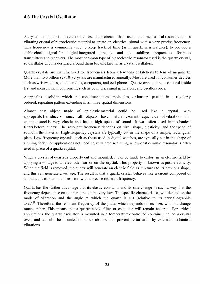
4.6 The Crystal Oscillator
A crystal oscillator is an electronic oscillator circuit that uses the mechanical resonance of a
vibrating crystal of piezoelectric material to create an electrical signal with a very precise frequency.
This frequency is commonly used to keep track of time (as in quartz wristwatches), to provide a
stable clock signal for digital integrated circuits, and to stabilize frequencies for radio
transmitters and receivers. The most common type of piezoelectric resonator used is the quartz crystal,
so oscillator circuits designed around them became known as crystal oscillators.
Quartz crystals are manufactured for frequencies from a few tens of kilohertz to tens of megahertz.
More than two billion (2×10⁹) crystals are manufactured annually. Most are used for consumer devices
such as wristwatches, clocks, radios, computers, and cell phones. Quartz crystals are also found inside
test and measurement equipment, such as counters, signal generators, and oscilloscopes.
A crystal is a solid in which the constituent atoms, molecules, or ions are packed in a regularly
ordered, repeating pattern extending in all three spatial dimensions.
Almost any object made of an elastic material could be used like a crystal, with
appropriate transducers, since all objects have natural resonant frequencies of vibration. For
example, steel is very elastic and has a high speed of sound. It was often used in mechanical
filters before quartz. The resonant frequency depends on size, shape, elasticity, and the speed of
sound in the material. High-frequency crystals are typically cut in the shape of a simple, rectangular
plate. Low-frequency crystals, such as those used in digital watches, are typically cut in the shape of
a tuning fork. For applications not needing very precise timing, a low-cost ceramic resonator is often
used in place of a quartz crystal.
When a crystal of quartz is properly cut and mounted, it can be made to distort in an electric field by
applying a voltage to an electrode near or on the crystal. This property is known as piezoelectricity.
When the field is removed, the quartz will generate an electric field as it returns to its previous shape,
and this can generate a voltage. The result is that a quartz crystal behaves like a circuit composed of
an inductor, capacitor and resistor, with a precise resonant frequency.
Quartz has the further advantage that its elastic constants and its size change in such a way that the
frequency dependence on temperature can be very low. The specific characteristics will depend on the
mode of vibration and the angle at which the quartz is cut (relative to its crystallographic
axes).[8]
Therefore, the resonant frequency of the plate, which depends on its size, will not change
much, either. This means that a quartz clock, filter or oscillator will remain accurate. For critical
applications the quartz oscillator is mounted in a temperature-controlled container, called a crystal
oven, and can also be mounted on shock absorbers to prevent perturbation by external mechanical
vibrations.
26
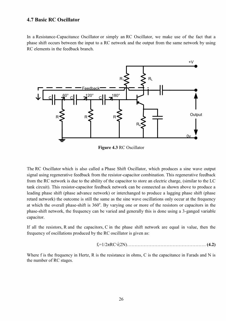
4.7 Basic RC Oscillator
In a Resistance-Capacitance Oscillator or simply an RC Oscillator, we make use of the fact that a
phase shift occurs between the input to a RC network and the output from the same network by using
RC elements in the feedback branch.
R R R
R1 RL
Re
C C C
Output
+V
0v
Feedback
60° 120° 180°
Figure 4.3 RC Oscillator
The RC Oscillator which is also called a Phase Shift Oscillator, which produces a sine wave output
signal using regenerative feedback from the resistor-capacitor combination. This regenerative feedback
from the RC network is due to the ability of the capacitor to store an electric charge, (similar to the LC
tank circuit). This resistor-capacitor feedback network can be connected as shown above to produce a
leading phase shift (phase advance network) or interchanged to produce a lagging phase shift (phase
retard network) the outcome is still the same as the sine wave oscillations only occur at the frequency
at which the overall phase-shift is 360o. By varying one or more of the resistors or capacitors in the
phase-shift network, the frequency can be varied and generally this is done using a 3-ganged variable
capacitor.
If all the resistors, R and the capacitors, C in the phase shift network are equal in value, then the
frequency of oscillations produced by the RC oscillator is given as:
fr=1/2πRC√(2N)……………………………………………. (4.2)
Where f is the frequency in Hertz, R is the resistance in ohms, C is the capacitance in Farads and N is
the number of RC stages.
27
4.8 Summary
This chapter introduces with the concept of different types of oscillators. It mainly emphasizes on the
harmonic oscillators, since this is the type of oscillator that this project deals with.
The chapter also describes briefly about the oscillators and also their working principle.
This project deals with a modified version of the Royer Oscillator, which will be discussed in the later
chapters.

28
Chapter 5
Transmitter & Receiver Circuits
5.1 Introduction
Operation of devices that comply with Wireless Power Transfer relies on magnetic induction between
planar coils. Two kinds of devices are distinguished, namely devices that provide wireless power and
devices that consume wireless power referred to as Mobile Devices. Power transfer always takes place
from a Base Station to a Mobile Device. For this purpose, a Base Station contains a subsystem referred
to as a Power Transmitter that comprises a Primary Coil, and a Mobile Device contains a subsystem
referred to as a Power Receiver comprises a Secondary Coil. In fact, the Primary Coil and Secondary
Coil form the two halves of a coreless resonant transformer. Appropriate Shielding at the bottom face
of the Primary Coil and the top face of the Secondary Coil, as well as the close spacing of the two
coils, ensures that power transfer occurs with an acceptable efficiency. In addition, this Shielding
minimizes the exposure of users to the magnetic field.
5.2 Transmitter circuit
In electronics and telecommunications a transmitter or radio transmitter is an electronic device which,
with the aid of antenna, produces radio waves. The transmitter itself generates a radio
frequency alternating current, which is applied to the antenna. When excited by this alternating current,
the antenna radiates radio waves. In addition to their use in broadcasting, transmitters are necessary
component parts of many electronic devices that communicate by radio, such as phones,
wireless, Bluetooth enabled devices, garage door openers, two-way radios in aircraft, ships, and
spacecraft, radar sets, and navigational beacons. The term transmitter is usually limited to equipment
that generates radio waves for communication purposes; or radiolocation, such as radar and
navigational transmitters.
5.3 Working Principal of Transmitter circuits
A Power Transmitter comprises two main functional units, namely a power conversion unit and a
communications and control unit. The primary coil acts as the magnetic field generating element of the
power conversion unit. The control and communications unit regulate the transferred power to the
level that the power receiver requests. A base station may contain multiple transmitters in order to
serve multiple mobile devices simultaneously (a power transmitter can serve a single power receiver at
a time only). Finally, the system unit comprises ofall other functionality of the base station, such as
input power provisioning, control of multiple power transmitters, and user interfacing.

29
5.4 Types of Transmitters
Pressure transmitters
Differential pressure transmitters
Flow transmitters
Level transmitters
Temperature transmitters
Radio transmitters
Television transmitters
Radar transmitters
Sonar transmitters
Power transmitters etc.
5.5 Block Diagram of Power Transmitter
Fig 5.1Functional block diagram of Power Transmitter

30
5.6 Receiver Circuit
The secondary receiver coils are similar designs to the primary sending coils. Running the secondary at
the same resonant frequency as the primary ensures that the secondary has low impedance at the
transmitter's frequency and that the energy is optimally absorbed. To remove energy from the
secondary coil, different methods can be used, the AC can be used directly or rectified and a regulator
circuit can be used to generate DC voltage.
5.7 Working principle of Receiver circuit
The receiver’s main purpose is to charge a battery. A simple battery charging theory is to run current through the battery, and apply a voltage difference between the terminals of the battery to reverse the
chemical process. By doing so, it recharges the battery. There are other efficient and faster ways to
charge the battery, but it requires a large amount of energy which the wireless battery charger cannot
obtain, yet. Therefore, in our design, we use a straight forward method to charge the battery.
Fig 5.2 Full-wave Rectifier circuit
A full-wave rectifier is chosen for the project due to its simplicity and efficiency in converting the AC
signal. The full-wave rectifier is consisted of four diodes. Since the power received by the receiver will
be relatively low and the signal frequency is high, the diodes are required to have a very low turn on
voltage and operating frequency at 900 MHz. For this reason, a Schottky diode could be chosen for the
design.
At the output of the rectifier, the signal is not a fully DC signal yet. Thus, by adding a capacitor and a
resistor can smooth out the output to become DC signal. However, the time constant produced by the
capacitor and the resistor should be calculated carefully to fit the desired time constant.
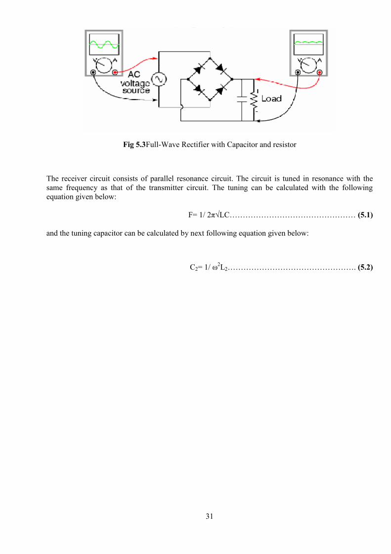
31
Fig 5.3Full-Wave Rectifier with Capacitor and resistor
The receiver circuit consists of parallel resonance circuit. The circuit is tuned in resonance with the
same frequency as that of the transmitter circuit. The tuning can be calculated with the following
equation given below:
F= 1/ 2π√LC………………………………………… (5.1)
and the tuning capacitor can be calculated by next following equation given below:
C2= 1/ ω2L2…………………………………………. (5.2)

32
5.8 Block Diagram of Power Receiver circuit
Fig 5.4Functional block diagram of a Power Receiver
5.9 Summary
This chapter gives the general ideas of transmitter and receiver circuit. Moreover, it also presents the
different types of transmitter that exists.

33
Chapter 6
Design and Implementation of Our Project
6.1 Introduction
The idea of wireless charging came from the idea of wireless energy transfer. The first thoughts were
to charge a pacemaker wirelessly. Deep study on that particular topic revealed that pacemakers already
had a good enough life time. So, the idea of charging it was not a feasible one.
Further study about wireless power transfer came up with the idea of a wireless charger for the low
power devices such as mobile phones, camera etc.
The main idea was to charge these low power devices using inductive coupling. The overall process
required a transmitter and a receiver.
The transmitter would convert a D.C. power to high frequency A.C. power. This alternating current
would create an alternating magnetic field to transmit energy.
The receiver, on the contrary, would receive that energy by means of an induced A.C. voltage. A diode
rectifier would convert the A.C. voltage to D.C. and this voltage would be supplied to load through a
voltage controller.

34
6.2 Transmitter Module
The transmitter module of our project is made up of a D.C. power source, an oscillator circuit
(commonly known as an inverter) and a transmitter coil.
The D.C. power source provides a constant D.C. voltage to the input of the oscillator circuit. There,
this D.C. power is converted to a high frequency A.C. power and is supplied to the transmitter coil.
The transmitter coil, energized by the high frequency A.C. current, produces an alternating magnetic
field.
The following block diagram (Figure 6.1) gives a general idea of the transmitter module:
D.C. Power Source Oscillator Transmitter Coil
Figure 6.1 Block Diagram of the Transmitter Module
6.2.1 The D.C. Power Source
The D.C. Power Source consists of a simple step down transformer and a rectifier circuit. The
transformer steps down the voltage to a desired level and the rectifier circuit convert the A.C. voltage
to D.C.

35
6.2.2 The Oscillator Circuit
The prototype oscillator Circuit designed for the project is a modified Royer oscillator (Figure 6.2).
This oscillator circuit is incredibly simple yet a very powerful design. Very high oscillating current can
be achieved with this circuit depending on the semiconductor used. Here high current is necessary to
increase the strength of the magnetic field. Although Insulated Gate Bipolar Transistors (IGBT) is
recommended for this type of oscillator, but IGBTs have limitations in high frequencies. Thus, a
HEXFET Power MOSFET was used for its properties. The HEXFET is ultra-low on resistance and has
an operating temperature of 175°C. It has an advanced process technology and is very fast in
switching.
Vdc C1
R1
R3
L1
Q1
R2
R4
L2
C L
Q2
D2
D1
Figure 6.2The Modified Royer Oscillator

36
6.2.3 Operation of the Oscillator Circuit
The circuit consists of with two chokes labeled L1 and L2, two semiconductors (Here N-channel
Enhancement power-MOSFETS) labeled Q1 and Q2, a resonating capacitor labeled C and an inductor
(here the transmitter coil) labeled L. Cross-coupled feedback is provided via the diodes D1 and D2. R1,
R3 and R2, R4 are the biasing network for MOSFETS Q1 and Q2.
When power is applied, DC current flows through the two sides of the coil and to the transistors’ drain. At the same time the voltage appears on both gates and starts to turn the transistors on. One transistor
is invariably a little faster than the other and will turn on more. The added current flowing in that side
of the coil does two things. One, it takes away drive from the other transistor. Two, the auto-
transformer action impresses a positive voltage on the conducting transistor, turning it hard on. The
current would continue to increase until the coil (transformer) saturates. The resonating capacitor C
causes the voltage across the primary to first rise and then fall in a standard sine wave pattern.
Assuming that Q1 turned on first, the voltage at the drain of Q1’s will be clamped to near ground while
the voltage at Q2’s drain rises to a peak and then falls as the tank formed by the capacitor and the coil primary oscillator through one half cycle.
The oscillator runs at the frequency determined by the inductance of the coil, the capacitor value and to
a lesser extent, the load applied to the secondary (Source coil).
The operating frequency is the familiar formula for resonance,
F= 1/2 × π × (LC)…………………………………………… (6.1)
6.2.4 The Transmitter Coil
For this project the transmitter coil was constructed with 6mm copper tube with a diameter of 16.5cm
(6.5 inches) and a length of 8.5cm.
From the equation of inductance of a single layer air core coil[8]
we get,
L = 0.001 N2
(a/2)2 / (114a + 254l) H
L = 0.001×22× (0.165/2)
2 / ((114×0.165) + (254×0.085)) H
L = 0.674 µH
6.2.5 The Transmitter Circuit as a Whole

37
The transmitter module as a whole is given below:
Figure 6.3 Transmitter Module
The circuit diagram of the transmitter circuit is given below:
R1
R2
R3 R4
R5
L1 L2
CC C C C C C C L
IRF540 IRF540
D1
D2
LED
+30V
0V
Figure 6.4 Transmitter Circuit

38
6.2.6 Components Used in the Transmitter Module
The list of components that were used in the transmitter circuit is given in the following table:
Component’s Name Component’s Value or code
Voltage Source, Vdc 30V
Capacitor, C 6.8nF
Resistor, R1 1k ohm
Resistor, R2 10k ohm
Resistor, R3 94 ohm
Resistor, R4 94 ohm
Resistor, R5 10k ohm
Diode, D1 D4148
Diode, D2 D4148
MOSFET,Q1 IRF540
MOSFET, Q2 IRF540
Radio Frequency Choke,L1 8.6 µH
Radio Frequency Choke, L2 8.6 µH
Transmitter coil, L 0.674 µH
Table 6.1 Transmitter Components
In addition, one heat sink was used with each MOSFET to keep them cool and avoid their damage
during overheating.

39
6.3 Receiver Module
The receiver module of our project is made up of a receiver coil, a rectifier circuit and a voltage
regulator IC.
An A.C. voltage is induced in the receiver coil. The rectifier circuit converts it to D.C. and the voltage
regulator IC helps to maintain a constant limited voltage at the load.
The following block diagram (Figure 6.5) gives a general idea of the receiver module:
Receiver Coil Rectifier Voltage Regulator ICLoad/ Low Power
Device
A.C.
Voltage
D.C.
Voltage
Limited
D.C.
Voltage
Figure 6.5 Block Diagram of the Receiver Module
6.3.1 Receiver Coil
For this project the receiver coil was constructed with 18 awg (American Wire Gauge) copper wire
with a diameter of 8cm.
From the equation of inductance of a single layer air core coil [8]
we get,
L = 0.001 N2
(a/2)2 / (114a + 254l) H
L = 0.001×32× (0.08/2)
2 / ((114×0.08) + (254×0.01)) H
L = 1.235 µH

40
6.3.2 Rectifier
A rectifier is an electrical device that converts alternating current (AC), which periodically reverses
direction, to direct current (DC), which flows in only one direction. The process is known as
rectification. Physically, rectifiers take a number of forms, including vacuum tubediodes, mercury-arc
valves, solid-state diodes, silicon-controlled rectifiers and other silicon-based semiconductor switches.
A diode bridge is an arrangement of four (or more) diodes in a bridge circuit configuration that
provides the same polarity of output for either polarity of input. When used in its most common
application, for conversion of an alternating current (AC) input into direct current a (DC) output, it is
known as a bridge rectifier. A bridge rectifier provides full-wave rectification from a two-wire AC
input, resulting in lower cost and weight as compared to a rectifier with a 3-wire input from a
transformer with a center-tapped secondary winding.
The essential feature of a diode bridge is that the polarity of the output is the same regardless of the
polarity at the input. The diode bridge circuit is also known as the Graetz circuit after its inventor,
physicist Leo Graetz.
Figure 6.6 shows a diode bridge rectifier.
The 4 diodes labeled D1 to D4 are arranged in series pairs with only two diodes conducting current
during each half cycle (Figure: 6.6).
AC
D1
D4
D3
D2
Load
Figure 6.6 Diode Bridge Rectifier

41
6.3.3 Operation of a Diode Bridge Rectifier
During the positive half cycle of the supply, diodes D1 and D2 conduct in series while diodes D3 and
D4 are reverse biased and the current flows through the load as shown in Figure 6.7.
D1
D4
D3
D2
Load
Off
Off
Figure 6.7 Positive Half- Cycle
During the negative half cycle of the supply, diodes D3 and D4 conduct in series, but diodes D1 and
D2 switch off, as they are reverse biased. The current flowing through the load is the same direction as
before(Figure 6.8).
D1
D4
D3
D2
Load
Off
Off
Figure 6.8 Negative Half- Cycle
As the current flowing through the load is unidirectional, so the voltage developed across the load is
also unidirectional.

42
6.3.4 Rectifier Used in the Receiver Module
The rectifier used in the receiver module is similar to the one discussed above. The only addition to it
is a smoothing capacitor. The smoothing capacitor converts the full-wave rippled output of the rectifier
into a smooth DC output voltage. Figure 6.9 shows a rectifier with a smoothing capacitor.
D1
D4
D3
D2
Load
C
Figure 6.9 Rectifier with a Smoothing Capacitor
6.3.5 Voltage Regulator IC
A voltage regulator is an electricalregulator designed to automatically maintain a constant voltage
level. A voltage regulator may be a simple feed-forward design or may include negative
feedbackcontrol loops. It may use an electromechanical mechanism, or electronic components.
Depending on the design, it may be used to regulate one or more AC or DC voltages.
In this project, LM 7805 voltage regulator IC was used since it allowed no more than 5v to the output.
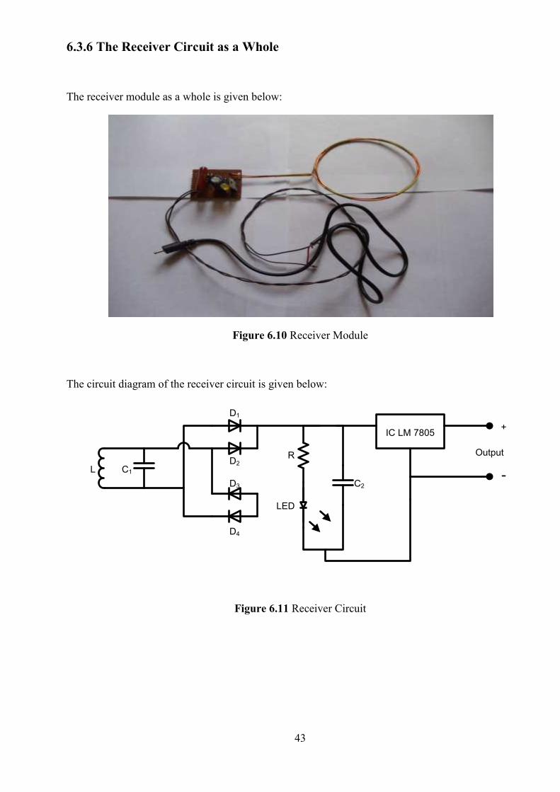
43
6.3.6 The Receiver Circuit as a Whole
The receiver module as a whole is given below:
Figure 6.10 Receiver Module
The circuit diagram of the receiver circuit is given below:
IC LM 7805
L C1
R
C2
D1
D2
D3
D4
LED
Output
+
-
Figure 6.11 Receiver Circuit

44
6.3.7 Components Used in the Receiver Module
The list of components that were used in the receiver circuit is given in the following table:
Component’s Name Component’s Value or code
Diode, D1 D4007
Diode, D2 D4007
Diode, D3 D4007
Diode, D4 D4007
Capacitor, C1 6.8 nF
Capacitor, C2 220 µF
Resistor, R 1k ohm
Voltage Regulator IC IC LM 7805
Receiver coil, L 1.235 µH
Table 6.2 Receiver Components

45
6.4 Performance and Analysis
30v was provided to the input of the oscillator circuit.
6.6v was calculated across the transmitter coil.
When the distance between transmitter coil and receiver coil was 0 inches, the voltage measured across
the receiver coil was 4.1v. So the energy transfer efficiency was 62.12%.
When the distance between transmitter coil and receiver coil was 1 inch, the voltage measured across
the receiver coil was 4v. So the energy transfer efficiency was 60.61%.
When the distance between transmitter coil and receiver coil was 2 inches, the voltage measured across
the receiver coil was 2.25v. So the energy transfer efficiency was 34.09%.
When the distance between transmitter coil and receiver coil was 3 inches, the voltage measured across
the receiver coil was 0.08v. So the energy transfer efficiency was 1.21%.
When the distance between transmitter coil and receiver coil was 4 inches, the voltage measured across
the receiver coil was 0.04v. So the energy transfer efficiency was 0.61%.
When the distance between transmitter coil and receiver coil was 5 inches, the voltage measured across
the receiver coil was 0.02v. So the energy transfer efficiency was 0.30%.
When the distance between transmitter coil and receiver coil was 6 inches, the voltage measured across
the receiver coil was 0.01v. So the energy transfer efficiency was 0.15%.
When the distance between transmitter coil and receiver coil was 7 inches, the voltage measured across
the receiver coil was 0v. So the energy transfer efficiency was 0%.
The above mentioned measurements suggests that the system is suitable for use only when the distance
between transmitter coil and receiver coil ranges from 0 to about 1.5 inches.
6.5 Summary
This chapter discussed about all the components and circuits used in the following project. The chapter
also described some of these circuits and components briefly. In addition, the chapter gives a brief idea
of the performance of the circuits.

46
Chapter 7
Possible Applications of Our Project
7.1 Introduction
The main inspiration of our project came from the concept of getting rid of electrical wires, which
means wires from all electrical system. This is the next big challenge of this century. Thus it is not
possible to get it done overnight. Therefore we started from small scale; that is low power electronic
devices. Our main concern is to make sure that these low power electronic devices get charge
efficiently and easily. So that in future we could take this concept to a whole new level, large scale
including national grid.
Here in this project we used the concept of inductive coupling to transfer energy. Since our project is
merely a prototype so its commercial viability is not yet possible. In this section we therefore came up
with some modifications and enhancement to our project which could make it as consumable product.
Figure 7.1 Wireless electricity (WiTricity) concept

47
7.2 Installing the Receiver Circuit inside the Body of the Devices
A receiver comprises a means for receiving the energy from the alternating magnetic field and
transferring it to a mobile or other device. The receiver can also comprise electronic components or
logic to set the voltage and current to the appropriate levels required by the mobile device, or to
communicate information or data to and from the pad. The system may also incorporate efficiency
measures that improve the efficiency of power transfer between the charger and receiver. As a matter
of fact for installing receiving circuit inside the electronic device initially the whole circuit has to be
converted onto a chip, which is small enough to fit inside the device. The receiving circuit consists of
coil and control circuit. In order to do that the most preferred way is to design a PCB with IC
components. Sometimes special casing for holding this extra circuit is used, mostly for cell phones. On
the other hand other larger devices usually do not require such casing. Therefore the use of adapter,
charging dock or other plug-in methods for charging these devices will not be required.
Fig 7.2wireless power receiver chip

48
7.3 Transmitter Circuit as the Charging Dock
A transmitter unit comprises a primary coil, which creates a magnetic field by applying an alternating
current to a winding, coil, or any type of current carrying wire. Transmitter unit also consists of safety
devices like voltage and current sensor, heat sink, controller circuit, inverter and an oscillator. In order
to convert the whole transmitter circuit into a dock or pad, except the transmitter coil all the devices
are burned onto a chip using modern day technology. Therefore we could design a transmitter circuit
which looks more like a pad. A prototype of such transmitter circuit burned onto a single circuit is
given below:
Fig 7.3 Transmitter circuit chip
7.4 Charging Mid-range Power Devices
In this project so far it has been discussed about charging devices of low-rated power devices such as;
cell-phones, digital camera, electric shaver, gaming-console, wireless mouse, wireless keyboard and
portable music players etc. In order to charge mid-range devices such as laptops, portable-television,
speakers, IPS-battery and car battery etc. (mid-range usually means devices that work on voltage of
15V-30V) the original design has to be modified to some extent. The modification includes; use of
high rated rectifier, diodes, control circuits and very efficient cooling system i.e. use of fan or liquid
cooling system. Therefore the circuit can provide power transfer for long period of time efficiently. In
general the working principal for both the transmitter and receiver units is same for the mid-range
wireless charging system. Therefore if the system works for low-rated power devices then it should
work for the mid-range or even high-range power devices.

49
7.5 Charging Electric Vehicles
Nowadays environmental pollution is a matter of concern for all of us. Carbon emission from vehicles
is making our environment poisonous day by day. Government is trying different methods to make
carbon emission to minimal. The latest breakthrough is electric vehicle. The problem now is to provide
a suitable charging system for these vehicles, so that people do not feel hesitate to have electric
vehicle. In this section we are introducing wireless charging system for charging up vehicles.
Fig 7.4 Wireless charging system
The wireless charging system will enable an electric vehicle's battery to be recharged without the
hassle of cords or connections. This hands free charging technology is based on highly resonant
magnetic coupling which transfers electric power over short distances without physical contact,
allowing for safer and more convenient charging options for consumer and commercial electric
vehicles. The high efficiency wireless energy transfer technology will require no plugs or charging
cords. Instead, a magnetic field from a source resonator on the ground is aligned with a capture
resonator mounted underneath a vehicle.

50
7.5.1 Benefits of the Technology
The benefits of using this technology are:
1. Convenience and simplicity for electric vehicle owners
2. Enables easy, automatic charging by simply parking a vehicle in a garage or parking spot
3. System activates the moment a vehicle is aligned with the charging pad
4. Minimal driver action needed and no plugs or charging cords needed
7.5.2 Safety Features
The system also provides some safety features:
1. Non-radiative power transfer uses a magnetic near field
2. Very little energy transferred to extraneous or off-resonant objects
3. Can fully charge an electric vehicle at a rate comparable to most residential plug-in chargers,
which can be as fast as 4 hours
4. Weather resistant
5. Environmental factors such as snow or rain would have no effect on the wireless energy
transfer
6. Less vulnerable to tampering or accidental damage when compared to corded charging
alternatives
7. Low maintenance for commercial and public installations
8. No moving / mechanical parts
9. Effective across larger air gaps, allowing for a greater vehicle ground clearance
10. Accommodates greater misalignment between vehicle resonator and stationary resonator,
meaning that perfect parking accuracy is not required
The source of the power can be located on a garage floor or embedded in a paved parking spot. The
energy receiver will be located under the vehicle. The concept is given in the figure below:
Fig 7.5 Charging multiple numbers of vehicles

51
7.6 Commercial Possibility
There is already huge demand for wireless power transmission system. Mostly the renowned electronic
giants like Sony, Samsung, Panasonic, Toshiba, Apple and Bose etc. have shown huge interest in this
technology. The fact is that we have already made huge advancement in electronic side, but
introducing wireless technology in this sector has made it possible to capture huge market. Wireless
technology is what people wanted for long. Besides, there is a huge demand in defense sector as well.
In general, wireless power transmission is a breakthrough to the electronic industry. This technology
has helped the industry to explore into new dimension which they have never imagined.
7.7 Summary
The chapter discussed about the future prospects of the technology used in our project. The wireless
power transmission is a new technology with a huge potential. It could be the future of this world.
The chapter also discussed about the different possible technologies that could be implemented with
the idea of our project.
Lastly, the chapter tells about the commercial possibility of this recent technology.

52
Chapter 8
Discussions and Conclusions
8.1 Discussions
In our project the main goal was to design and implement a system that transmits power to charge low
power devices without wire. In this purpose, a transmitter circuit was implemented. At the end of the
transmitter circuit an antenna was connected, which transmits the power. Another antenna was used to
receive the power wirelessly from the transmitter circuit. In this project hollow copper pipes were used
as antenna, because it has high Q-factor and high power handling performance.
It requires a huge task to implement the whole project. During implementation a number of remarkable
problems were faced and were solved as well. Though these implementation sessions require patience,
it gives a great pleasure after successful solution.
8.2 Problems and Solutions
The problems that were faced during the testing period as well as the solution are given below:
Since wireless charging is a recent technology, there is not enough information available about this
technology. The work that has been done in this project is totally new and different than any other
charging method.
Solid copper wire of a satisfying diameter is rarely available in the local market. The one that was
available and was used first did not perform well with the design. So, copper tube was used instead.
The first thought was to use vacuum tube transistors, in the oscillator circuit, which provides much
higher power than the typical power MOSFETs. Later this idea was eliminated since vacuum tube was
not available in the local market.
In the local market low equivalent series resistance (ESR) capacitors are not available. For the
oscillator circuit presented, low ESR polypropylene capacitors are highly recommended to handle the
high current flowing through the LC tank. Moreover, other type of capacitor creates high spikes in the
sinusoidal wave at the LC tank circuit and affects the MOSFETs. However, Mylar capacitors at first
were used which has polyester as the dielectric. The circuit was found unstable with this type of
capacitor. Later metalized plastic polypropylene capacitors were used which performed much better.
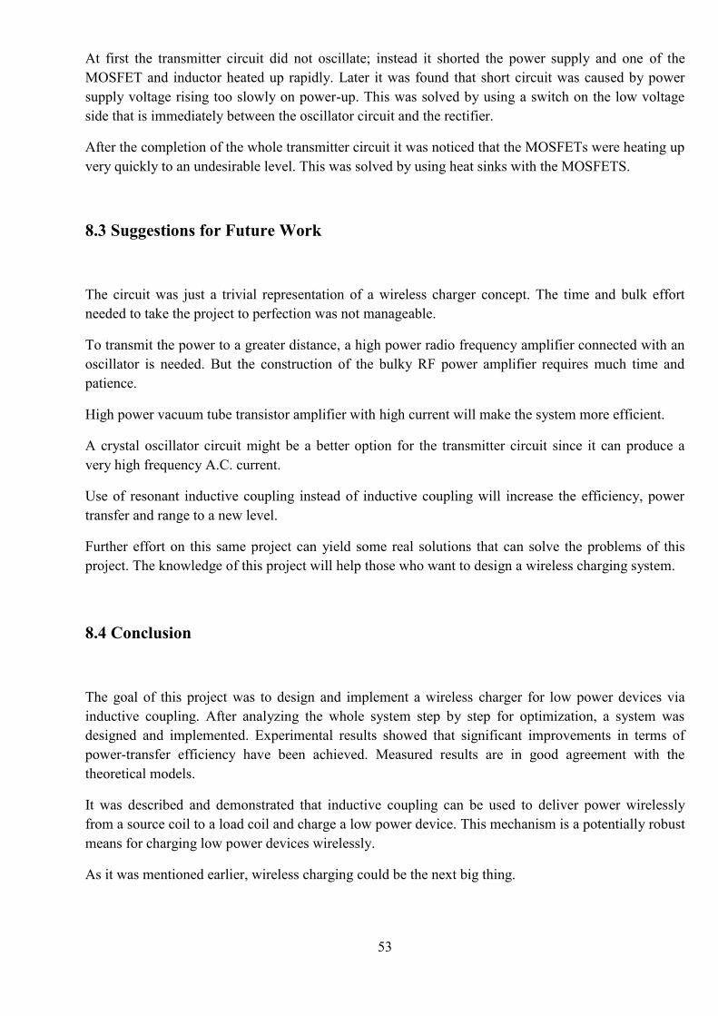
53
At first the transmitter circuit did not oscillate; instead it shorted the power supply and one of the
MOSFET and inductor heated up rapidly. Later it was found that short circuit was caused by power
supply voltage rising too slowly on power-up. This was solved by using a switch on the low voltage
side that is immediately between the oscillator circuit and the rectifier.
After the completion of the whole transmitter circuit it was noticed that the MOSFETs were heating up
very quickly to an undesirable level. This was solved by using heat sinks with the MOSFETS.
8.3 Suggestions for Future Work
The circuit was just a trivial representation of a wireless charger concept. The time and bulk effort
needed to take the project to perfection was not manageable.
To transmit the power to a greater distance, a high power radio frequency amplifier connected with an
oscillator is needed. But the construction of the bulky RF power amplifier requires much time and
patience.
High power vacuum tube transistor amplifier with high current will make the system more efficient.
A crystal oscillator circuit might be a better option for the transmitter circuit since it can produce a
very high frequency A.C. current.
Use of resonant inductive coupling instead of inductive coupling will increase the efficiency, power
transfer and range to a new level.
Further effort on this same project can yield some real solutions that can solve the problems of this
project. The knowledge of this project will help those who want to design a wireless charging system.
8.4 Conclusion
The goal of this project was to design and implement a wireless charger for low power devices via
inductive coupling. After analyzing the whole system step by step for optimization, a system was
designed and implemented. Experimental results showed that significant improvements in terms of
power-transfer efficiency have been achieved. Measured results are in good agreement with the
theoretical models.
It was described and demonstrated that inductive coupling can be used to deliver power wirelessly
from a source coil to a load coil and charge a low power device. This mechanism is a potentially robust
means for charging low power devices wirelessly.
As it was mentioned earlier, wireless charging could be the next big thing.
54
References
[1] Russell M Kerchner and George F Corcoran, ―Alternating-Current Circuits‖, pp. 273-324, 1960.
[2] G. Grandi, M.K. Kazimierczuk, A. Massarini, ―Optimal Design of Single-Layer Solenoid Air-Core
Inductors for High Frequency Applications‖, Circuit Systems, Vol. 1, pp. 358-361, 1997.
[3] A. Kurs, A. Karalis, R. Moffatt, J. D. Joannopoulos, P. Fisher, M. Soijacic, ―Wireless Power Transfer via Strongly Coupled Magnetic Resonances‖, Massachusetts Institute of Technology, 2007 Science, Vol. 317. no. 5834, pp. 83— 86, 2007
[4] Jacob Millman and Christos C. Halkias, ―Integrated Electronics: Analog and Digital Circuits and
Systems‖, pp. 103-107, 2007
[5] Muhammad H. Rashid, ―Power Electronics: Circuits, Devices, and Applications‖, pp.37-63, 2nd
Edition, 2000
[6] Robert L. Boylestad and Louis Nashelsky,‖Electronic Devices and Circuit Theory‖,9th
Edition,2006, pp. 79-82
[7] William H.Hayt,Jr. and John A.Buck,‖Engineering Electromagnetics‖,7th Edition,2006,pp.292-299
[8] http://info.ee.surrey.ac.uk/Workshop/advice/coils/air_coils.html
[9]http://en.wikipedia.com
[10] http://www.smeter.net/electronics/solnoid3.php
[11] http://inhabitat.com/tag/resonant-inductive-coupling-charger/
[12] http://www.delphi.com
[13] http://seminarprojects.com