
EXTENDED SUMMARY - SD-ETTI UPB
48
UNIVERSITY „POLITEHNICA” OF BUCHAREST ETTIB DOCTORAL SCHOOL Decision No. 515 from 01.07.2020 EXTENDED SUMMARY SMART MODULES FOR SECURING THE ELECTRONIC EQUIPMENT AGAINST TAMPERING PhD student: Eng. DanielCiprian Vasile DOCTORAL COMMITTEE President Prof. Gheorghe Brezeanu, PhD Eng. from Univ. Politehnica București PhD supervisor Prof. Paul Svasta, PhD Eng. from Univ. Politehnica București Reviewer Prof. Adriana Vlad, PhD Eng. from Univ. Politehnica București Reviewer Prof. Alexandru Șerbănescu, PhD Eng. from Academia Tehnică Militară Reviewer Sci. Res. I Liviu Coșereanu, PhD Phys. from INCD Aerospațială ”Elie Carafoli” BUCHAREST 2020
-
Upload
khangminh22 -
Category
Documents
-
view
5 -
download
0
Transcript of EXTENDED SUMMARY - SD-ETTI UPB

UNIVERSITY „POLITEHNICA” OF BUCHAREST
ETTIB DOCTORAL SCHOOL
Decision No. 515 from 01.07.2020
EXTENDED SUMMARY
SMART MODULES FOR SECURING THEELECTRONIC EQUIPMENT AGAINST TAMPERING
PhD student: Eng. DanielCiprian Vasile
DOCTORAL COMMITTEE
President Prof. Gheorghe Brezeanu, PhD Eng. from Univ. Politehnica BucureștiPhD supervisor Prof. Paul Svasta, PhD Eng. from Univ. Politehnica BucureștiReviewer Prof. Adriana Vlad, PhD Eng. from Univ. Politehnica BucureștiReviewer Prof. Alexandru Șerbănescu, PhD Eng. from Academia Tehnică MilitarăReviewer Sci. Res. I Liviu Coșereanu, PhD Phys. from INCD Aerospațială
”Elie Carafoli”
BUCHAREST 2020


Contents
List of figures iii
List of abbreviations v
1 Introduction 11.1 Presentation of the doctoral field . . . . . . . . . . . . . . . . . . . . . . 11.2 The purpose of the thesis . . . . . . . . . . . . . . . . . . . . . . . . . . 21.3 Content of the thesis . . . . . . . . . . . . . . . . . . . . . . . . . . . . 2
2 Attacks on electronic security circuits 32.1 Cryptanalysis of cryptographic systems . . . . . . . . . . . . . . . . . . 32.2 Sidechannel attacks . . . . . . . . . . . . . . . . . . . . . . . . . . . . 42.3 Physical Intrusions . . . . . . . . . . . . . . . . . . . . . . . . . . . . . 5
2.3.1 Measures to reduce physical intrusion attacks . . . . . . . . . . 6
3 Tamper detection circuits current state 73.1 Protection of electronic security circuits against physical intrusions . . . 73.2 Conductive networks . . . . . . . . . . . . . . . . . . . . . . . . . . . . 73.3 Passive Tamper Detection Circuits . . . . . . . . . . . . . . . . . . . . . 83.4 Active Tamper Detection Circuits . . . . . . . . . . . . . . . . . . . . . 83.5 Structure of an intrusion protection circuit . . . . . . . . . . . . . . . . 9
4 Active tamper detection circuits 114.1 Innovative doublelayer conductive network for active tamper
detection circuits . . . . . . . . . . . . . . . . . . . . . . . . . . . . . . 114.2 Active tamper detection circuit based on LFSR generator . . . . . . . . 124.3 Active tamper detection circuit based on the pulse response analysis of
the conductive network . . . . . . . . . . . . . . . . . . . . . . . . . . . 164.4 Active tamper detection circuit with dual function: temperature
variation detection and statistical intrusion detection . . . . . . . . . . . 194.5 Innovative conductive network with triple layer structure increasing
efficiency in detecting intrusions . . . . . . . . . . . . . . . . . . . . . . 214.6 Technological aspects of the manufacture of conductive networks on
dielectric flexible foils . . . . . . . . . . . . . . . . . . . . . . . . . . . 25
i

4.7 Specialized active tamper detection circuit for triple layer conductivenetworks . . . . . . . . . . . . . . . . . . . . . . . . . . . . . . . . . . . 26
5 Complementary security functions of the triple layer conductive network 295.1 Securing electronic security circuits . . . . . . . . . . . . . . . . . . . . 295.2 Authentication of electronic security circuits . . . . . . . . . . . . . . . 30
6 Conclusions 316.1 Original contributions . . . . . . . . . . . . . . . . . . . . . . . . . . . . 316.2 List of original works . . . . . . . . . . . . . . . . . . . . . . . . . . . . 37
Bibliography 39
ii

List of figures
3.6 Principle schematic of an active tamper detection circuit. . . . . . . . . 83.7 Schematic diagram of an ESC protection circuit. . . . . . . . . . . . . . 93.8 Structure of ESC and TDC ensemble. . . . . . . . . . . . . . . . . . . . 10
4.1 Conductive network traces made on a PCB. . . . . . . . . . . . . . . . . 124.2 ATDC reference diagram. . . . . . . . . . . . . . . . . . . . . . . . . . 124.3 Equivalent diagram of the conductive network connected to pins PE9
and PE11. . . . . . . . . . . . . . . . . . . . . . . . . . . . . . . . . . . 134.4 The logic diagram of the pseudorandom generator based on the
Gollmann cascade. . . . . . . . . . . . . . . . . . . . . . . . . . . . . . 134.5 The composition of the probing impulses of the conductive network. . . 144.6 Experimental tamper detection circuit. . . . . . . . . . . . . . . . . . . . 154.7 Captures of the pulses at pins PE9, PE11, PC6 and PE5. . . . . . . . . . 154.11 ATDC principle schematic. . . . . . . . . . . . . . . . . . . . . . . . . . 164.13 Amplification and acquisition circuit. . . . . . . . . . . . . . . . . . . . 174.22 Spectral power variation for pulses of 46.4ns in case of increasing
the capacity in parallel with the conductive network (normed power,x10−4 ). . . . . . . . . . . . . . . . . . . . . . . . . . . . . . . . . . . . 18
4.23 Spectral power variation for pulses of 46.4ns in case of increasing theresistance in series with the conductive network (normed power, x10−4 ). 18
4.26 Normalized power of the probing signal as a function of temperature. . 204.27 Variation of statistical parameters depending on the increase of capacity. 204.28 Variation of statistical parameters depending on the increase of
resistance. . . . . . . . . . . . . . . . . . . . . . . . . . . . . . . . . . . 204.29 Geometric structure of the conductive network used in simulation. . . . 214.35 Improved conductive network. . . . . . . . . . . . . . . . . . . . . . . . 224.36 Conductive network unaffected by intrusion: red trace signal
amplitude on resistor R_1, blue trace signal amplitude measuredat a point on the conductive trace on layer 3. . . . . . . . . . . . . . . . 22
4.37 Conductive network affected by intrusion: red trace signal amplitudeon resistor R_1, blue trace signal amplitude measured at a point onthe conductive trace on layer 3. . . . . . . . . . . . . . . . . . . . . . . 22
4.40 The structure of the conductive network consisting in two active areas. . 23
iii

4.43 Conductive network output characteristic (simulation): NT nointrusion, TC1_O C1 open circuit, TC2_O C2 open circuit. . . . . . 23
4.45 Conductive network output characteristic (experimental test): NT nointrusion, TC1_O C1 open circuit, TC2_O C2 open circuit. . . . . . 24
4.48 Conductive network output characteristic (simulation): NT nointrusion, TC1_O C1 open circuit, TC1_S C1 short circuit betweentraces, TC2_O C2 open circuit, TC2_S C2 short circuit betweentraces. . . . . . . . . . . . . . . . . . . . . . . . . . . . . . . . . . . . . 24
4.52 Conductive network output characteristic (experimental test): NT nointrusion, TC1_O C1 open circuit, TC1_S C1 short circuit betweentraces, TC2_O C2 open circuit, TC2_S C2 short circuit betweentraces. . . . . . . . . . . . . . . . . . . . . . . . . . . . . . . . . . . . . 24
4.56 Conductive traces printed with SW180 paste. . . . . . . . . . . . . . . . 254.58 Testing of 0.1mm PES foil at bending under different radii of
curvature. For radii smaller than 2mm, conductive trace cracks appear. . 254.59 Principle diagram of ATDC intended for probing the triple layer
conductive network. . . . . . . . . . . . . . . . . . . . . . . . . . . . . 264.61 Experimental ATDC consisting of NUCLEOL432KC development
board, interface circuit and conductive network. . . . . . . . . . . . . . 264.62 Conductive network output signal (channel 1, blue trace) and signal
detected at the output of the logarithmic amplifier (channel 2, red trace). 274.63 Conductive network output characteristic: NT not tampered, TC1_O
C1 open circuit, TC1_S C1 short circuit, TC2_O C2 open circuit,TC2_S C2 short circuit. . . . . . . . . . . . . . . . . . . . . . . . . . . 27
4.66 Conductive network output characteristic: behavior at temperaturevariations. . . . . . . . . . . . . . . . . . . . . . . . . . . . . . . . . . . 28
4.69 Conductive network PES 0.1mm: amplitude differences (modulus)between physical intrusions and thermal attack limits. . . . . . . . . . . 28
5.2 Limits of values acquired at the output of the 0.3mm PCB conductivenetwork, for temperature variations between −20C and 80C. . . . . . 29
5.4 Examples of conductive network responses at 80MHz and 120MHz. . . 305.5 Representation of the quantization domains corresponding to the
probing frequencies of the conductive network i and i+ 1. . . . . . . . 30
iv

List of abbreviations
ADC analog to digital converterAI artificial intelligenceARM family of processor architectures (Arm Limited)ASIC application specific integrated circuitATDC active tamper detection circuitDAC digital to analog converterePTFE expandedpolytetrafluoroethyleneESC electronic security circuitFLASH nonvolatile memoryFPGA field programmable gate arrayGPIO general purpose input/outputHASH dispersion functionHSM harware security moduleInternet global system of interconnected computer networksIoT internet of thingsIT information technologyLDS laser direct structuringLFSR linear feedback shift registerNFSR nonlinear feedback shift registerNVRAM nonvolatile RAMPC personal computerPCB printed circuit boardPES poly ether sulfonePOS point of salePWM pulse width modulationRAM random access memoryRF radiofrequencySCA side channel attacksTDC tamper detection circuitUART universal asynchronous receivertransmitter
v

vi

Chapter 1
Introduction
1.1 Presentation of the doctoral field
The current digital age is based on communications and data processing and ischaracterized by changes in an accelerated rate. Electronic equipment includeselectronic circuits (hardware) and computer applications (software, firmware) thatimplement their functions. New technologies offer countless possibilities and areasfor development, but their use can expose the user to risks. For valuable resources,such as information, hardware, software and firmware, assessing these risks can bedifficult and depends on the environment in which these resources are located.
The security of information resources is part of the evolution of any organizationand is represented by protecting the profit, ensuring the security of members or thevalues they hold. This profile can also be defined for structures and organizations atnational or international levels. The costs involved in protecting information resourcesdepend on each computer and communications system. To be an efficient system,security costs must not outweigh the benefits of using protected resources.
Electronic security circuits (ESCs) are the modules responsible for the security ofinformation resources in electronic equipment. They contain both logic components(such as logic gates, processors, memories, FPGA and CPLD circuits etc.) and analogcomponents (linear power supplies, noise sources, sensors etc.).
Security data is any information processed inside electronic equipment (data,functions, protocols, routines software and firmware) that the manufacturer wishes toprotect against unauthorized access. This security data is processed inside ESC usingdedicated integrated circuits that implement the computer application.
Cryptography provides the mathematical means necessary for the protection ofinformation in digital format (security data). They consist of functions, protocols andprinciples that ESC implements.

Smart modules for securing the electronic equipment against tampering
1.2 The purpose of the thesisThe study included in this thesis aimed to find innovative and effective solutions toprotect the ESCs against the most important intrusions, in terms of the effectivenessof cryptanalytic attack, namely physical intrusions and attacks by temperaturevariation. The solutions proposed in the thesis consist in designing a coating withsensory characteristics to protect the ESC, made of a conductive network, and anelectronic circuit to analyze the change in electrical characteristics of the conductivenetwork.
The aim was for the physical structure, which consists of a special conductivenetwork, to provide several detection functions, namely: shortcircuit detection andinterruption of conductive network paths, detection of temperature variations andshielding of protected circuits.
In the case of intrusion detection circuits, the analysis and experimental testingof several detection methods, to establish the efficiency in the cases of interest, wereconsidered.
1.3 Content of the thesisChapter 1 presents the importance of electronic security circuits in the context ofdata communications and security of information resources. The areas of use of thesecircuits are highlighted in the context of modern technologies.
Chapter 2 contains a summary of attacks on electronic security circuits, such ascryptanalysis, side channel attacks and physical intrusions.
Chapter 3 describes the components of an intrusion detection circuit and thecurrent state of the solutions available in this field.
Chapter 4 includes the contributions to the development of conductive networksand active intrusion detection circuits, which work in conjunction with them. Twotypes of conductive networks are studied: double layer network and triple layernetwork. Methods for probing conductive networks by active intrusion detectioncircuits are presented. They can detect physical intrusions, intrusion attempts and heatattacks (temperature variations at the conductive network level).
Chapter 5 extends the scope of intrusion detection systems, presented inChapter 4, to the protection of electronic security circuits or copyright in computerapplications.
Chapter 6 presents the original contributions and the list of original works.The bibliography represents the last chapter of the thesis and contains the works
consulted during the thesis.
2
Chapter 2
Attacks on electronic security circuits
An important aspect of ESC security is that it must protect the security data stored orused in the processes inside it: cryptographic keys, secret data, passwords, firmwareetc. The protection must be active throughout the life of ESC, unconditioned bythe presence of the power supply. In this sense, ESCs are protected by specializedcircuits, equipped with sensors that constantly monitor various state parametersand detect intrusion attempts, while ensuring low power consumption. Intrusion(tampering) detection circuits are made with specialized integrated circuit (ASIC),logic gates, programmable circuits (FPGA, CPLD) or microcontrollers, to whichare attached various sensors dedicated to this purpose. In the event of an intrusionbeing detected, the dedicated circuit takes the scheduled action so as not to disclosethe security data, which generally consists of quickly deleting it. Usually, thesecurity data is stored in a volatile RAM memory and the deletion is performed byinterrupting its power supply.
Types of attacks on electronic security circuits.
Attacks on ESCs can be grouped into the following categories:
• Cryptanalysis of cryptographic systems;
• Side channel attacks;
• Physical intrusions.
2.1 Cryptanalysis of cryptographic systemsCryptanalysis studies the cryptographic systems in order to find weaknesses in thefunctions implemented in them that could help decrypt data without knowing theencryption key [1]. In the risk analysis associated with cryptanalytic attacks it isconsidered that the encryption algorithm is known. Cryptanalytic attacks can beclassified according to the type of information that the attacker has at his disposal [1],as follows:

Smart modules for securing the electronic equipment against tampering
• Ciphertextonly. In this attack scenario, only encrypted text is used andthe attacker is assumed to have passive capabilities to monitor encryptedcommunication. Even if the attacker does not know the clear text, he still hassome information about the clear text.
• Chosenplaintext. In this scenario, the attacker has the option to choose theplaintext and obtain the corresponding ciphertext. In modern cryptographydifferential cryptanalysis is a typical example of an attack with chosen text.This attack is similar to the chosen ciphertext attack.
• Adaptive chosenplaintext. It is similar to the attack with chosen text with thedifference that the attacker chooses subsequent clear texts based on informationlearned from previous encryptions.
• Relatedkeys. As with plain text attack, the attacker gains access to encryptedtext with associated keys. The keys are not known to the attacker but are in amathematical relationship known to him.
Cryptanalytic attacks can be characterized from the point of view of the necessaryresources, as follows:
• Time. The duration of the attack depends on the number of steps to beperformed.
• Memory. Every attack needs memory to store working variables and vectors.Each type of attack requires a different volume of memory.
• Required data volume. Depending on the type of attack, the required datavolume (plain text, ciphertext) must be of a certain size.
2.2 Sidechannel attacksSidechannel attacks (SCAs) use any information, unintentionally provided, fromelectronic devices that implement cryptographic functions. This information can bein the following forms [2] [3] [4]: processing time, sound, electromagnetic waves,dissipated power, supply currents etc. These attacks depend on how ESCs aredesigned and how cryptographic functions are implemented.
The FIPS 1402 standard [5] defines four types of SCA attacks: power analysis,runtime analysis, error induction, and TEMPEST. These attacks are described asfollows:
1. Power analysis. Attacks based on power consumption can be divided into twocategories, Simple Power Analysis (SPA) and Differential Power Analysis(DPA). SPA involves a direct analysis of the waveforms of signals thatcharacterize the consumption of power and the execution times of individual
4

Attacks on electronic security circuits
instructions by an ESC during the execution of a cryptographic function.DPA has the same purpose as SPA but uses advanced statistical methods andspecialized techniques (eg timefrequency analysis) to analyze variations inpower consumption.
2. Timing Analysis. Duration analysis attacks are based on the accuratemeasurement of the execution time of mathematical operations associated with acryptographic function. The time information collected is analyzed to determinethe relationship between the ESC inputs and the cryptographic keys used by thealgorithm or process in question.
3. Fault Induction. Fault induction attacks use external stimuli, such asmicrowave radio signals, extreme temperatures, and manipulation of the supplyvoltage to cause ESC processing errors. The analysis of these errors and theoccurrence model can be used in reverse engineering of the application runningin ESC, in order to reveal the implementation characteristics of cryptographicfunctions and, subsequently, cryptographic keys.
4. TEMPEST. TEMPEST analysis involves the remote detection and collection ofinformation from unwanted electromagnetic signals emitted by a ESC.
2.3 Physical IntrusionsIn addition to protection measures against cryptanalytic attacks or side channelattacks, ESCs must be protected against physical intrusions so that access to itselectronic components is impossible. Physical intrusion can be defined as any actionaimed at gaining access to electronic components or data buses that make up anelectronic circuit. The connection to the data buses between the logic circuits of theESC ensures the obtaining of important information from its internal processes.
Unauthorized access to the ESC’s electronic circuit can cause significant damage,such as:
• Obtaining the cryptographic key. This can lead to the decryption of thecommunications of the device that incorporates an ESC or the decryption ofthe communications from the entire network to which the electronic module isconnected. Thus, the confidentiality of the data can no longer be ensured.
• Intervention on the messages communicated by ESC. Message integrity can nolonger be ensured.
• Assumption of ESC identity by another entity. An attacker may transmit falseinformation to network entities as if it were transmitted by the ESC in question.
• Modify messages transferred to the network to introduce errors. Theauthenticity of the messages is thus compromised.
5

Smart modules for securing the electronic equipment against tampering
2.3.1 Measures to reduce physical intrusion attacks
Protection against physical intrusion attacks is characterized by the following types ofactions:
• Tamper detection: is the ESC’s automatic determination of an attempt tocompromise physical security.
• Tamper evidence: is the external indication of the electronic equipmentcontaining ESC regarding the attempt to compromise physical security.
• Tamper response: is the automatic action performed by ESC as soon as itdetects the intrusion. The ESC shall take action against unauthorized use ordisclosure of security data stored therein.
6
Chapter 3
Tamper detection circuits currentstate
3.1 Protection of electronic security circuits againstphysical intrusions
ESC security is achieved through a set of multilevel protection mechanisms. The firstlevel is the physical one: the electronic circuits are protected by a special housing,which does not allow unauthorized entry into the circuit. They are made of metallicmaterials and meet the following requirements: they are watertight and do not haveslots or perforations that could favor the access of specialized probes (optical) at thelevel of electronic circuits.
The second most important level is the protection of electronic circuits andsecurity data. An attacker should not have access to these circuits, but if it managesto pass the first level of protection, ESC has a specialized circuit that reacts in theway of protecting the security data. The response time is very short and the effect iscomplete, in the sense that all security data is deleted.
The solution that ensures this level of protection is the introduction, between themetal housing and the protected circuit, of a special conductive layer that is sensitiveto intrusions the conductive network. This network is periodically probed withsignals by the Tamper Detection Circuit (TDC). When this circuit detects an intrusion,it performs specific security data protection functions: fast deletion of this data andexecution of a special routine for deleting sensitive data inside the ESC processor.
Depending on how the probing signals of this protective layer are analyzed,intrusion detection circuits are classified into passive circuits and active circuits.
3.2 Conductive networks
To ensure a high level of protection, conductive networks (conductive meshes), madein the form of a printed circuit covering both the ESC and TDC [6], are used. The

Smart modules for securing the electronic equipment against tampering
conductive network may be flexible, made of thin printed foils, or rigid, made ofprinted circuit boards (PCBs), joined so as not to result in gaps that would facilitateintrusions or the introduction of probes to analyze the inside of the ESC. Any attemptto penetrate these structures determines the generation of the intrusion event.
For these conductive networks to be effective in terms of penetration attempts,both the width of the traces and the space between them must be small, generally lessthan 0.2mm.
3.3 Passive Tamper Detection CircuitsPassive tamper detection circuits are based on the monitoring of electrical or logicallevels, the variation of these levels outside the limits determines the triggering of theintrusion response process (tamper response). Depending on the consumption regimeused, the parameters can be checked continuously or at a predefined period.
To ensure an increased level of security of protected data (cryptographic keys,random sequences and other secret data), intrusion detection integrated circuits canbe equipped with nonvolatile RAM and a realtime clock. The realtime clockprovides the required time stamp in many cryptographic processes but also recordsthe time when the intrusion event was detected. As nonvolatile RAM is a part ofthe integrated circuit, it is intended to store a cryptographic key, necessary for theencryption of data volumes (ESC firmware, security data etc.).
3.4 Active Tamper Detection CircuitsActive tamper detection circuits (ATDC) are based on the principle of testingthe conductive network by probing it with signals with appropriately chosencharacteristics. The probing signals are injected into the conductive network throughthe input port. At its output port, the signals are sampled and analyzed, with referenceto the initial signals. The principle diagram of such a circuit is presented in figure 3.6.
Figure 3.6: Principle schematic of an active tamper detection circuit.
Generally, probing signals are pulses that have variable parameters (period,
8

Tamper detection circuits current state
duration, shape) in order to make them impossible to reproduce in the event of abypass attack (deactivating an area of the conductive network and injecting falsepulses).
ATDC analyzes the effects that the conductive network exerts on the pulses thatpropagate through it. To perform this analysis, the signals resulting from the output ofthe conductive network are sampled and analyzed in the time and frequency domains.In this way, the dispersive characteristic of the conductive network can be exploited.This method involves using a fast analogtodigital converter and performing a largervolume of calculations than other methods.
As with passive intrusion detection circuits, ATDC can be affected byelectromagnetic interference both inside and outside the protected electronic circuit.To reduce this effect it is necessary to shield the conductive network inside andoutside. In this way, the effects of external electromagnetic interference will play auseful role in detecting intrusions by affecting the probing signals due to the voluntarydamage of the external shielding layer.
3.5 Structure of an intrusion protection circuit
ESCs are modules that are part of specialized electronic equipment, mainly dedicatedto data and communications protection. How ESC interacts with the intrusiondetection circuit and other types of attacks is shown in figure 3.7. The detectioncircuit constantly monitors the sensors, both during the operation of the equipmentand during the period when it is not powered. During the periods when it is notpowered (during transport, storage or maintenance), the detection circuit is poweredby a backup battery. In case of detection of such access (intrusion, outofboundschange of circuit temperature, change of supply voltage etc.), the detection circuitinterrupts the supply of nonvolatile RAM, to provoke the loss of security data, andgenerates an interrupt signal to the logic circuit of ESC (microprocessor, ASIC etc.)in order to delete the data from RAM and internal registers.
Figure 3.7: Schematic diagram of an ESC protection circuit.
9

Smart modules for securing the electronic equipment against tampering
The sensors used by TDC are: conductive network (for detecting physicalintrusions), temperature sensors, sensors for monitoring supply voltages, sensorsfor detecting the variation of the processor clock frequency and other circuits withmonitoring functions.
In order to protect the conductive network against external factors, including theelectromagnetic interference, the entire ESC protection circuit is enclosed in a rigidmetal case. This enclosure also protects against accidental physical intrusions. Figure3.8 exemplifies this method of ESC protection.
Figure 3.8: Structure of ESC and TDC ensemble.
The ESC is completely covered by the conductive network, except for theconnector through which it is powered (during operation) and the data is transferred.The metal enclosure, which covers this structure, is connected to the ground planeof the equipment. This enclosure improves the stability over time of the intrusiondetection circuit in order to reduce false triggers of intrusion events.
10
Chapter 4
Active tamper detection circuits
4.1 Innovative doublelayer conductive network foractive tamper detection circuits
In order to isolate the conductive traces from the possible electromagneticinterferences of ESC and ATDC (these being protected, as a whole, by ATDC), it isnecessary to introduce a separation ground plane, connected to the ground potential ofESC and ATDC. Thus, the printed circuit will contain two conductive layers (isolatedby a dielectric layer): one ground plane and one layer with a conductive network. Theground plane will be positioned between the module formed by ESC and ATDC andthe conductive network.
Flexible electromagnetic screen design
To ensure increased flexibility of the conductive network, the ground plane is madein a hatched form with square perforations, with side of 0.5mm, spaced at 1mm.Considering that the surfaces that make up the conductive network do not exceeda square with sides of 10cm (100 perforations / side), the shielding efficiency is89.5dB.
Conductive network design
The role of the conductive network is to prevent intrusions (perforations) in order togain access to ESC and ATDC. It is made in the form of thin traces, with a width ofless than 0.2mm, with a maximum space between paths of 0.2mm. The traces modellooks like meanders and they cover the entire surface, without leaving uncoveredspaces, and is made of a single conductive circuit (it has a single input and a singleoutput accessible at ATDC level). A sample of the conductive network is shown infigure4.1.
For conducting experimental tests, the conductive network was made of a printedcircuit board (PCB) of sticlotextolite type (FR4), with two layers of copper, with a

Smart modules for securing the electronic equipment against tampering
Figure 4.1: Conductive network traces made on a PCB.
thickness of 0.035mm. The printed circuit board has the size of 12.5 × 25cm, thethickness of 0.5mm, and the routes have the width and the distance between them of0.2mm. The first layer consists of conductive traces with the model shown in figure4.1, the second consists of a complete copper foil connected to the ground plane ofESC and ATDC.
4.2 Active tamper detection circuit based on LFSRgenerator
The tamper detection circuit, studied in the paper [7], consists of a microcontroller,the conductive network shown in figure 4.1 and a pulse formation circuit.STM32F4DISCOVERY development board (contains the STM32F407VGmicrocontroller) was used to perform the tests and measurements. The functionaldiagram of this circuit is presented in figure4.2.
Figure 4.2: ATDC reference diagram.
The microcontroller generates pulses at both ends of the conductive network inorder to mask the source of the probe pulses and to mislead a possible attacker who
12

Active tamper detection circuits
would try to simulate these pulses. The GPIO pins PE9 and PE11 are connected tothe conductive network and are configured as open drain outputs for channels 1 and 2of the internal clock circuit Timer 1, in PWM mode (Pulse Width Modulation). Theseoutput pins are configured in open drain mode to perform the logical AND functionrequired in this application. The equivalent scheme, with the concentrated parameters,is presented in figure 4.3.
Figure 4.3: Equivalent diagram of the conductive network connected to pins PE9 andPE11.
The principle of generation and acquisition of probing pulses
Probing pulses are synchronized using a pseudorandom sequence generator LFSR(LinearFeedback Shift Register). A modified Gollmann cascade configuration wasused for the ATDC circuit, as shown in [8]. The logic diagram of this generator ispresented in figure 4.4:
Figure 4.4: The logic diagram of the pseudorandom generator based on the Gollmanncascade.
This generator is used to decide which pulses are active at the output portsPE9 and PE11 (configured as alternative function 1 TIM1_CH1, respectively,TIM1_CH2). Timer1 is configured in PWM generation mode with the frequency of250kHz and is synchronized by the internal clock signal of the microcontroller (withthe frequency of 168MHz). At each period of 4µs, Timer1 enters the interrupt routineand, based on the output of the LFSR generator, the program determines whether
13

Smart modules for securing the electronic equipment against tampering
the probing pulse is generated. If the LFSR generator produces a bit 0, then theoutput Timer1 is disabled, otherwise the LFSR generator provides two bits that willdetermine the parameters of the generated pulses.
The relationship between D1 and D2 is D2 = D1 + d, where d is the propagationtime of the pulses through the conductive network, in this particular case d = 162ns.
The pulse composition mode is shown in figure 4.5 and is valid at any point ofthe conductive network and is due to the fact that ports PE9 and PE11 are configuredin open drain mode to obtain the logic function AND ( textit AND).
Figure 4.5: The composition of the probing impulses of the conductive network.
Pulses formation circuit
The pulse formation circuit is made using the TLV3501 [9] [10] comparator, used inthe hysteresis comparator configuration to increase noise immunity. Noise immunityis necessary because the pulses have slow fronts and the comparator can produceoscillations at the output at times when the input signal has values near the thresholdlevel.
Analysis of detected pulses
The pulses produced by the formation circuit, made with comparators, are analyzedby the clock circuits Timer8, channel 1 (TIM8_CH1), and Timer9, channel 1(TIM9_CH1), connected to pins PC6 and PE5, respectively (configured as alternativefunction 3). These clock circuits are configured in PWM analysis mode and performthe function of detecting pulse periods and durations.
To demonstrate the operation of ATDC, the experimental circuit presented infigure 4.6 was made. This circuit contains all the modules presented above: theprinted circuit board (PCB) of the conductive network (left side of the figure),the pulse formation circuit (right side of the figure) and the STM32F4Discoverydevelopment board (central part of the figure).
14

Active tamper detection circuits
Figure 4.6: Experimental tamper detection circuit.
The pulses measured at the pins PE9, PE11, PC6 and PE5 are shown in figure4.7, channels 1 to 4.
Figure 4.7: Captures of the pulses at pins PE9, PE11, PC6 and PE5.
The proposed method of generating probe pulses, based on a complex LFSRgenerator scheme, together with the principle of their composition during propagationthrough the conductive network do not allow determining the pulse parameters andsimulating the normal operation of the detection circuit.
Following experimental tests, ATDC achieves the following performances:
• detects variations of durations between pulses greater than 5.9ns;
• detects variations of pulse durations greater than 5.9ns;
• detects an increase in the total capacity of the conductive network by at least22pF ;
• detects physical intrusions made by cutting the conductive network and anyintervention that can change the duration and amplitude of the signals throughit.
15
Smart modules for securing the electronic equipment against tampering
4.3 Active tamper detection circuit based on the pulseresponse analysis of the conductive network
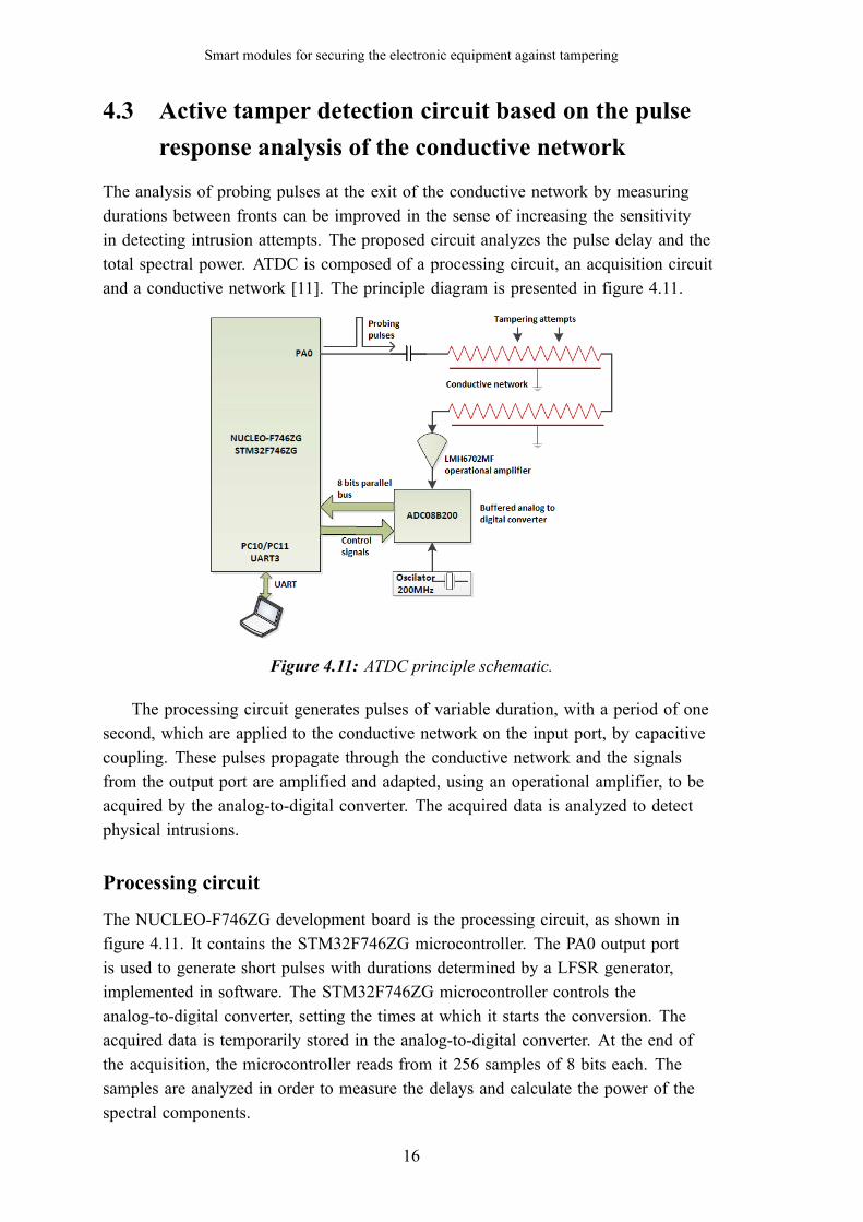
The analysis of probing pulses at the exit of the conductive network by measuringdurations between fronts can be improved in the sense of increasing the sensitivityin detecting intrusion attempts. The proposed circuit analyzes the pulse delay and thetotal spectral power. ATDC is composed of a processing circuit, an acquisition circuitand a conductive network [11]. The principle diagram is presented in figure 4.11.
Figure 4.11: ATDC principle schematic.
The processing circuit generates pulses of variable duration, with a period of onesecond, which are applied to the conductive network on the input port, by capacitivecoupling. These pulses propagate through the conductive network and the signalsfrom the output port are amplified and adapted, using an operational amplifier, to beacquired by the analogtodigital converter. The acquired data is analyzed to detectphysical intrusions.
Processing circuit
The NUCLEOF746ZG development board is the processing circuit, as shown infigure 4.11. It contains the STM32F746ZG microcontroller. The PA0 output portis used to generate short pulses with durations determined by a LFSR generator,implemented in software. The STM32F746ZG microcontroller controls theanalogtodigital converter, setting the times at which it starts the conversion. Theacquired data is temporarily stored in the analogtodigital converter. At the end ofthe acquisition, the microcontroller reads from it 256 samples of 8 bits each. Thesamples are analyzed in order to measure the delays and calculate the power of thespectral components.
16
Active tamper detection circuits
Acquisition circuit
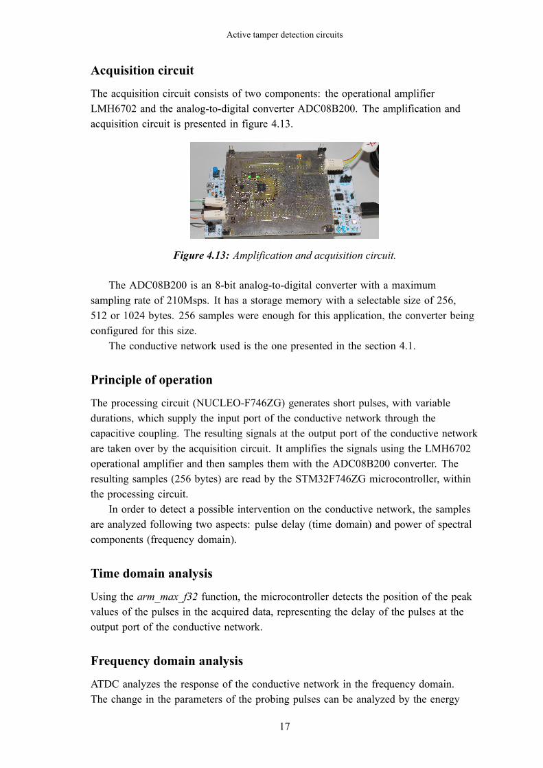
The acquisition circuit consists of two components: the operational amplifierLMH6702 and the analogtodigital converter ADC08B200. The amplification andacquisition circuit is presented in figure 4.13.
Figure 4.13: Amplification and acquisition circuit.
The ADC08B200 is an 8bit analogtodigital converter with a maximumsampling rate of 210Msps. It has a storage memory with a selectable size of 256,512 or 1024 bytes. 256 samples were enough for this application, the converter beingconfigured for this size.
The conductive network used is the one presented in the section 4.1.
Principle of operation
The processing circuit (NUCLEOF746ZG) generates short pulses, with variabledurations, which supply the input port of the conductive network through thecapacitive coupling. The resulting signals at the output port of the conductive networkare taken over by the acquisition circuit. It amplifies the signals using the LMH6702operational amplifier and then samples them with the ADC08B200 converter. Theresulting samples (256 bytes) are read by the STM32F746ZG microcontroller, withinthe processing circuit.
In order to detect a possible intervention on the conductive network, the samplesare analyzed following two aspects: pulse delay (time domain) and power of spectralcomponents (frequency domain).
Time domain analysis
Using the arm_max_f32 function, the microcontroller detects the position of the peakvalues of the pulses in the acquired data, representing the delay of the pulses at theoutput port of the conductive network.
Frequency domain analysis
ATDC analyzes the response of the conductive network in the frequency domain.The change in the parameters of the probing pulses can be analyzed by the energy
17
Smart modules for securing the electronic equipment against tampering
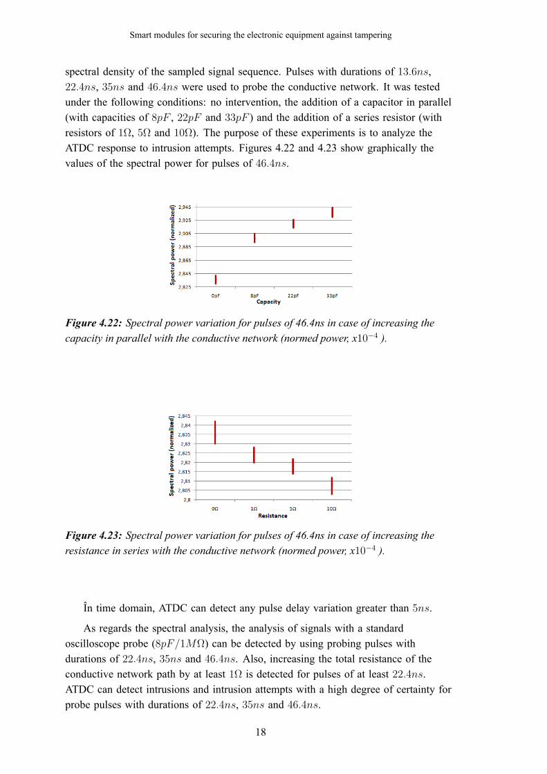
spectral density of the sampled signal sequence. Pulses with durations of 13.6ns,22.4ns, 35ns and 46.4ns were used to probe the conductive network. It was testedunder the following conditions: no intervention, the addition of a capacitor in parallel(with capacities of 8pF , 22pF and 33pF ) and the addition of a series resistor (withresistors of 1Ω, 5Ω and 10Ω). The purpose of these experiments is to analyze theATDC response to intrusion attempts. Figures 4.22 and 4.23 show graphically thevalues of the spectral power for pulses of 46.4ns.
Figure 4.22: Spectral power variation for pulses of 46.4ns in case of increasing thecapacity in parallel with the conductive network (normed power, x10−4 ).
Figure 4.23: Spectral power variation for pulses of 46.4ns in case of increasing theresistance in series with the conductive network (normed power, x10−4 ).
În time domain, ATDC can detect any pulse delay variation greater than 5ns.
As regards the spectral analysis, the analysis of signals with a standardoscilloscope probe (8pF/1MΩ) can be detected by using probing pulses withdurations of 22.4ns, 35ns and 46.4ns. Also, increasing the total resistance of theconductive network path by at least 1Ω is detected for pulses of at least 22.4ns.ATDC can detect intrusions and intrusion attempts with a high degree of certainty forprobe pulses with durations of 22.4ns, 35ns and 46.4ns.
18
Active tamper detection circuits
4.4 Active tamper detection circuit with dual function:temperature variation detection and statisticalintrusion detection
In this section, an ATDC is proposed which, in addition to detecting physicalintrusions, can detect temperature variation at the level of the protective coatingformed by the conductive network. From the point of view of ESC security, it ismuch more efficient to detect the exceeding of the temperature limits at the level ofthe outer shell of the assembly consisting of ESC and ATDC than to perform thisfunction at the level of the printed circuit board.
In addition to protection measures against collateral channel attacks based ontemperature variation, the paper also offers a solution for intrusion detection bystatistical analysis of the conductive network response to pulse probing.
The analysis of the ATDC behavior at the temperature variations, at the levelof the conductive network, is based on the study carried out within the paper[12]. Statistical methods of intrusion detection were studied in the paper [13]. Theexperimental analysis was performed using the electronic circuit shown in figure 4.11.
Analysis of the response of the conductive network to temperaturevariations
Given the variation of the resistance and capacitance parameters, which characterizethe paths of the conductive network, the probe pulses that propagate through thisstructure are affected differently at different temperatures. Therefore, calculatingthe signal strength at the output of the conductive network is an efficient method ofdetecting variations in the characteristics of this propagation medium depending onthe temperature variation. The calculations were performed in floating point format,simple precision, using native microcontroller instructions.
Statistical analysis of the conductive network response
In order to detect the physical intrusions, a more energy efficient solution (with asmall number of calculations) is the statistical approach for the analysis of sampledsignals. The statistical parameters used in this paper are: arithmetic mean, root meansquare (RMS), standard deviation and variance. ATDC calculates these statisticalparameters and compares them with reference values to detect tampering attempts.
ATDC response to temperature variations
Temperature variation tests were performed using the ESPEC Temperature Chamber,model SH241. The tests were performed by varying the temperature in the range of−20oC÷100oC, with temperature stabilization at each temperature stage (10oC steps).
19

Smart modules for securing the electronic equipment against tampering
The acquired values of the normed power of the signal are presented in figure4.26. These values are used for relative comparisons in order to establish theoccurrence of the physical intrusion situation. From the analyzed data, the quasilinearvariation of the power is observed having a negative slope. ATDC is able tounambiguously detect the temperature in the conductive network.
Figure 4.26: Normalized power of the probing signal as a function of temperature.
Intrusion detection based on statistical analysis
Experimental testing simulated a possible intervention on the conductive networkand consisted of increasing the capacity in parallel with the conductive network(capacitors with capacities of 5pF , 10pF , 15pF , 20pF , 25pF ) and series resistancewith the conductive network (resistors with resistors of 1Ω, 2Ω, 3Ω, 5Ω, 10Ω).The experimental results are represented graphically in the figures 4.27 and 4.28.Experimental results demonstrate the efficiency of ATDC for increasing seriesresistance by more than 10Ω and increasing total capacity by more than 10pF .
(a) RMS (b) variance
Figure 4.27: Variation of statistical parameters depending on the increase of capacity.
(a) RMS (b) varianță
Figure 4.28: Variation of statistical parameters depending on the increase of resistance.
20

Active tamper detection circuits
4.5 Innovative conductive network with triple layerstructure increasing efficiency in detectingintrusions
The main requirements for conductive networks used to protect the ESC are to ensurean increased sensitivity to tampering attempts and the impossibility of replicating theprobing signal used by ATDC.
The study contained in this section is based on the article [14] and proposes aninnovative type of conductive network made of three conductive layers, isolated withdielectric layers. The first layer, arranged inwards, is a compact layer connected tothe ground potential and has two important roles: reference plane for probing signalsand electromagnetic shield between the assembly consisting of ESC and ATDC andconductive traces probed with signals (layers 2 and 3 ). Layer 2 (intermediate),contains a very fine conductive network (routes with thickness < 0.2mm anddistances between them < 0.2mm) with meander pattern. This is the layer used byATDC for the analysis of probing signals. The third outward layer is not directlyprobed by ATDC but is used to facilitate intrusion detection. The geometry of thepaths on this layer copies the one on the intermediate layer, with the differencethat they form closed circuits. In order to determine the behavior of the conductivenetwork in case of physical intrusions, the structure presented in figure 4.29 was used.
Figure 4.29: Geometric structure of the conductive network used in simulation.
Analyzing the signals induced in layer 3, this structure does not allow thedetermination of the characteristics of the probing signals used by ATDC. Thesesignals have very small amplitudes and do not have a reference ground plane, beingcircuits galvanically isolated from the rest of the structure. If an attacker tries toconnect to the conductive paths of layer 2, he should decommission areas of theconductive network on layer 3.
A conductive network measuring 30mm × 30mm has been designed withmeanders that perform inductive and capacitive couplings at different signalpropagation lengths in order to produce multiple resonances at low frequencies. TheANSYS ®SIwave 2016.2.0 application was used to simulate this conductive network,shown in figure 4.35.
21

Smart modules for securing the electronic equipment against tampering
Figure 4.35: Improved conductive network.
The simulation was performed in the frequency range 0Hz ÷ 500MHz. Thesimulation results for this structure are presented in figure 4.36, for the case of thedetection layer is unaffected, and in figure 4.37, for the case of the physical intrusionwas performed.
Figure 4.36: Conductive network unaffected by intrusion: red trace signal amplitudeon resistor R_1, blue trace signal amplitude measured at a point on the conductivetrace on layer 3.
Figure 4.37: Conductive network affected by intrusion: red trace signal amplitude onresistor R_1, blue trace signal amplitude measured at a point on the conductive traceon layer 3.
When creating the intrusion, from the two graphs it is observed the increase ofthe resonance points and the decrease of the frequencies at which these resonancestake place. Using an appropriate method for analyzing these resonances, ATDC canquickly detect an intrusion without exposing the signal path to the attacker. Structuressimilar to the one shown in figure 4.35 can be combined to obtain the area neededto cover the entire ESC. On layer 2 the conductive paths are connected in series, tocreate the signal path, and on layer 3 each zone forms a closed circuit.
22

Active tamper detection circuits
Triple layer conductive network extended structure
In the paper [15] it was evaluated the behavior in the frequency domain of a structureconsisting of two square areas, with sides of 30mm, the traces and spaces betweenthem having a width of 0.2mm. This structure is shown in figure 4.40. The workingprinciple of the assembly formed by this conductive network and ATDC was proposedfor publication in the patent application [16].
Figure 4.40: The structure of the conductive network consisting in two active areas.
As can be seen in figure 4.40, on layer 2, the conductive traces of the two zonesare connected in series and those on layer 3 form closed circuits, corresponding toeach zone. To validate the detection effect of the conductive network, it was madepractically in the form of a PCB, with a dielectric thickness of 0.3mm, with thesame characteristics as the simulated model. The following cases were analyzed:no intrusions, C1 affected by intrusion and C2 affected by intrusion. The results areshown in figure 4.43.
Figure 4.43: Conductive network output characteristic (simulation): NT no intrusion,TC1_O C1 open circuit, TC2_O C2 open circuit.
The output characteristic of the conductive network is presented in figure 4.45.As can be seen from the figures 4.43 and 4.45, starting with the frequency of30MHz, the conductive network is efficient in detecting open circuit intrusions.The amplitude differences between the unaffected state and the one affected by theintrusion of the conductive network are easily quantifiable for wide frequency ranges.
Triple layer conductive network shortcircuit intrusion analysis
Physical intrusions on conductive networks can be performed, in addition tointerrupting conductive traces, by creating short circuits between adjacent traces.
23

Smart modules for securing the electronic equipment against tampering
Figure 4.45: Conductive network output characteristic (experimental test): NT nointrusion, TC1_O C1 open circuit, TC2_O C2 open circuit.
Considering the circuit presented above, the following cases were analyzed bysimulation and experimental testing [17]: unaffected conductive network, shortcircuit between two adjacent traces and the interruption of the conductive path. A0.1mm thick PES (Poly Ether Sulfone) conductive network, printed with SW180conductive paste (Tatsuta Electric Wire & Cable Co. Ltd.), was tested. The result ofthe simulation is presented in figure 4.48.
Figure 4.48: Conductive network output characteristic (simulation): NT no intrusion,TC1_O C1 open circuit, TC1_S C1 short circuit between traces, TC2_O C2 opencircuit, TC2_S C2 short circuit between traces.
The conductive network has wide frequency ranges useful in intrusion detection.To validate the effects of intrusions on the conductive network, it was performedpractically and tested under the same conditions as the model used in the simulations.The measurements performed are shown in figure 4.52.
Figure 4.52: Conductive network output characteristic (experimental test): NT nointrusion, TC1_O C1 open circuit, TC1_S C1 short circuit between traces, TC2_O C2 open circuit, TC2_S C2 short circuit between traces.
Starting with the frequency of 85MHz, this structure can be used to securelydetect opencircuit and shortcircuit intrusions between adjacent traces. The twomodes of conductive network analysis (simulation and experimental testing)demonstrate its effectiveness in detecting interrupt or shortcircuit intrusionsperformed on the detection layer (3).
24

Active tamper detection circuits
4.6 Technological aspects of the manufacture ofconductive networks on dielectric flexible foils
The conductive network printed on PES foil was made with the help of screenprinting technology. For the realization of the conductive network, a graphic designwas conceived, which was later transposed in a screen printing screen with metallicfabric. Printing was done with SW180 conductive paste (TATSUTA) and DEKHorizon 08 printing equipment. Figure 4.56 shows details of foils printed withSW180 conductive paste on PES foil (0.2mm thick traces).
Figure 4.56: Conductive traces printed with SW180 paste.
An important property of the conductive network is its ability to be foldedwithout interrupting the conductive traces. A sample of conductive network,consisting of two linear traces, was tested by bending under different radii. Thetests, presented in figure 4.58, reveal that the conductive network can be bent witha minimum radius of 2mm without producing cracks.
(a) 3mm radius. (b) 2mm radius.
(c) 1mm radius. (d) 0.5mm radius.
Figure 4.58: Testing of 0.1mm PES foil at bending under different radii of curvature.For radii smaller than 2mm, conductive trace cracks appear.
An important aspect of this type of conductive paste is that it has a limitedmechanical strength, which is an advantage in making conductive networks forintrusion detection.
25
Smart modules for securing the electronic equipment against tampering
4.7 Specialized active tamper detection circuit for triplelayer conductive networks
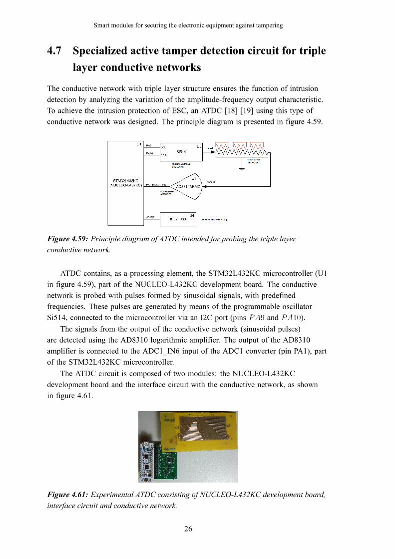
The conductive network with triple layer structure ensures the function of intrusiondetection by analyzing the variation of the amplitudefrequency output characteristic.To achieve the intrusion protection of ESC, an ATDC [18] [19] using this type ofconductive network was designed. The principle diagram is presented in figure 4.59.
Figure 4.59: Principle diagram of ATDC intended for probing the triple layerconductive network.
ATDC contains, as a processing element, the STM32L432KC microcontroller (U1in figure 4.59), part of the NUCLEOL432KC development board. The conductivenetwork is probed with pulses formed by sinusoidal signals, with predefinedfrequencies. These pulses are generated by means of the programmable oscillatorSi514, connected to the microcontroller via an I2C port (pins PA9 and PA10).
The signals from the output of the conductive network (sinusoidal pulses)are detected using the AD8310 logarithmic amplifier. The output of the AD8310amplifier is connected to the ADC1_IN6 input of the ADC1 converter (pin PA1), partof the STM32L432KC microcontroller.
The ATDC circuit is composed of two modules: the NUCLEOL432KCdevelopment board and the interface circuit with the conductive network, as shownin figure 4.61.
Figure 4.61: Experimental ATDC consisting of NUCLEOL432KC development board,interface circuit and conductive network.
26

Active tamper detection circuits
Description of the tampering detection process
The experimental implementation of this ATDC considered the testing of twoimportant features in the protection of ESC: the detection of physical intrusionsand the detection of temperature variations. To achieve optimal intrusion detectionresolution, 32 frequencies were used, with a 5MHz gap between them. The startingfrequency was chosen to be 50MHz, resulting in a domain with a maximumfrequency of 205MHz. The program in STM32L432KC controls the Si514 oscillatorso that it changes frequency every 250ms. After a duration of 20ms of internalstabilization of the signal generated by Si514, its output is activated for 300µs, timerequired for ADC1 to perform the conversion. Figure 4.62 shows a pulse generatedby Si514 and the pulse at the output of AD8310.
Figure 4.62: Conductive network output signal (channel 1, blue trace) and signaldetected at the output of the logarithmic amplifier (channel 2, red trace).
Tampering detection
ATDC testing, together with the triple layer conductive network, was performed inreal conditions of tampering such as interruption of the conductive trace and shortcircuit between adjacent traces on the detection layer (3) of the conductive network.The following cases were tested: conductive network is not tampered (NT), C1is opened (TC1_O), C1 is shortcircuited (TC1_S), C2 is opened (TC2_O), C2 isshortcircuited (TC2_S) . The conductive network made of 0.1mm thick PES foilprinted with SW180 conductive paste was analyzed. The result of the analysis ispresented in figure 4.63.
Figure 4.63: Conductive network output characteristic: NT not tampered, TC1_O C1 open circuit, TC1_S C1 short circuit, TC2_O C2 open circuit, TC2_S C2 shortcircuit.
27
Smart modules for securing the electronic equipment against tampering
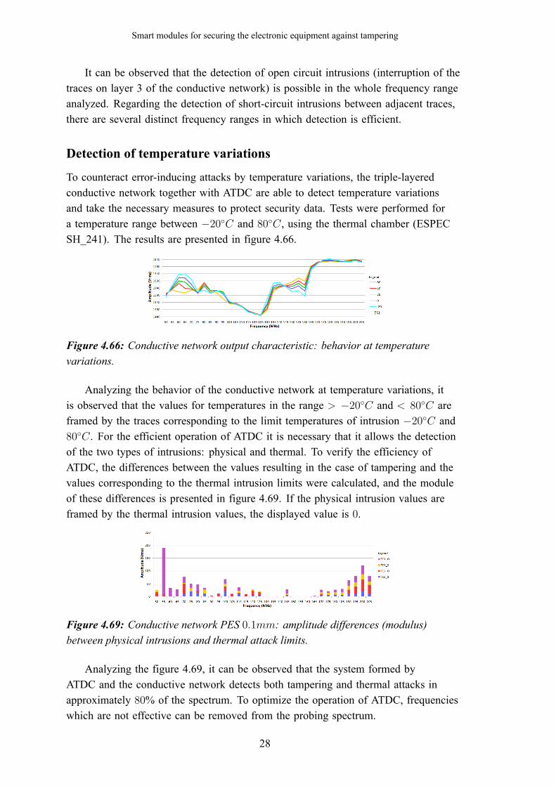
It can be observed that the detection of open circuit intrusions (interruption of thetraces on layer 3 of the conductive network) is possible in the whole frequency rangeanalyzed. Regarding the detection of shortcircuit intrusions between adjacent traces,there are several distinct frequency ranges in which detection is efficient.
Detection of temperature variations
To counteract errorinducing attacks by temperature variations, the triplelayeredconductive network together with ATDC are able to detect temperature variationsand take the necessary measures to protect security data. Tests were performed fora temperature range between −20C and 80C, using the thermal chamber (ESPECSH_241). The results are presented in figure 4.66.
Figure 4.66: Conductive network output characteristic: behavior at temperaturevariations.
Analyzing the behavior of the conductive network at temperature variations, itis observed that the values for temperatures in the range > −20C and < 80C areframed by the traces corresponding to the limit temperatures of intrusion −20C and80C. For the efficient operation of ATDC it is necessary that it allows the detectionof the two types of intrusions: physical and thermal. To verify the efficiency ofATDC, the differences between the values resulting in the case of tampering and thevalues corresponding to the thermal intrusion limits were calculated, and the moduleof these differences is presented in figure 4.69. If the physical intrusion values areframed by the thermal intrusion values, the displayed value is 0.
Figure 4.69: Conductive network PES 0.1mm: amplitude differences (modulus)between physical intrusions and thermal attack limits.
Analyzing the figure 4.69, it can be observed that the system formed byATDC and the conductive network detects both tampering and thermal attacks inapproximately 80% of the spectrum. To optimize the operation of ATDC, frequencieswhich are not effective can be removed from the probing spectrum.
28

Chapter 5
Complementary security functions ofthe triple layer conductive network
5.1 Securing electronic security circuitsThe output characteristic of the conductive network can be used in a special way tosecure the ESC, as follows: the signal levels acquired at discrete frequencies are usedto obtain a cryptographic key. ESC protection by ATDC covers the following cases:at startup (boot) and during operation.
At boot time, a cryptographic key is processed by testing the conductive networkat predefined frequencies. This key is used to decrypt the ESC firmware. After thefirmware is loaded correctly, it checks the state of the conductive network by probingit at predefined frequencies.
The study of this principle was performed in the paper [20], using theexperimental circuit presented above. For this principle to be effective, it is necessaryfor each conductive network to provide an unpredictable cryptographic key. Thevariation of the acquired values is determined by the quantization process of theADC, the ATDC noise and the thermal response of the conductive network.
Considering the operational thermal range between the values −20C and 80C,the conductive network is characterized by an operational band, bordered by themaximum and minimum traces, as shown in figure 5.2.
Figure 5.2: Limits of values acquired at the output of the 0.3mm PCB conductivenetwork, for temperature variations between −20C and 80C.
Figure 5.4 exemplifies, for two values of the probing frequencies (80MHz

Smart modules for securing the electronic equipment against tampering
and 120MHz), the response value ranges of the tested conductive networks,corresponding to the analyzed thermal range (between −20C and 80C).
(a) PCB 0, 3mm,80MHz.
(b) PCB 0, 3mm,120MHz.
Figure 5.4: Examples of conductive network responses at 80MHz and 120MHz.
Figure 5.4 shows that each tested conductive network has a unique answer, usablein setting up a cryptographic key. The cryptographic key can be obtained by dividingthe amplitude space into Qi,j quanta, with i representing the frequency Fi and j
representing the quanta number. Each quantum corresponds to a binary value, so thatconcatenating these values produces the cryptographic key KD. This way of dividingthe amplitude space is shown in figure 5.5.
Figure 5.5: Representation of the quantization domains corresponding to the probingfrequencies of the conductive network i and i+ 1.
This section proposes an innovative method of deriving cryptographic keys basedon the amplitudefrequency output characteristic of the conductive network, a methodthat simplifies cryptographic systems by eliminating the need to store secret data, andensures a high level of security for their internal processes. systems.
5.2 Authentication of electronic security circuitsIdentification data, in the case of authentication, can be obtained from the responseof the conductive network by quantizing it at discrete frequencies. The uniqueidentification of the equipment containing a ESC, requires that the sequences obtainedfrom the amplitudefrequency characteristic to be unique. To ensure the uniqueness,the following methods can be implemented: unique conductive networks, adding RLCelements, applying a HASH function, probing at different frequencies etc.
30

Chapter 6
Conclusions
This chapter summarizes the conclusions resulting from the research applied in thedoctoral thesis. In the first section, the original contributions resulting from theresearch activity are listed. The second section contains the list of papers publishedby the author and the research reports from the doctoral program.
6.1 Original contributions
Chapter 2
1. I studied the types of attacks on electronic security circuits: cryptanalysis ofcryptographic systems, side channel attacks and physical intrusions [11, 12, 13,14, 15].
2. I emphasized the need to ensure the physical protection of electronic securitycircuits [11, 12, 13, 14, 15].
Chapter 3
1. I analyzed the characteristics of electronic security circuit protection systemsagainst physical intrusions [11].
2. I have documented the role and types of conductive networks used in electronicsecurity circuit protection systems [11, 12].
3. I analyzed the properties and disadvantages of passive intrusion detectioncircuits [11, 12, 13, 14, 15].
4. I studied the active intrusion detection circuits. We analyzed the principle ofoperation and the current stage of development [11, 12].
5. I have proposed a schematic diagram and a physical structure of the assemblyconsisting of the electronic security circuit and the intrusion detection circuit[11].

Smart modules for securing the electronic equipment against tampering
Chapter 4
Section 4.1
1. I made a conductive network consisting of a ground layer and a layer withconductive traces, intended for signal probing. The ground layer improvesintrusion detection properties. It has two roles: reference plane for probingsignals propagating through conductive traces and electromagnetic shield [1,11].
Section 4.2
1. I designed an active tamper detection circuit consisting of a processing circuit,based on the STM32F407 microcontroller, and a conductive network interfacecircuit, consisting of hysteresis comparators [1, 11].
2. I established a method for generating probing pulses by using a LFSRpseudorandom sequence generator [1, 11].
3. I established a method for implementing probing pulses, characterized by theirsimultaneous generation at the two ports of the conductive network [1, 11].
4. The analysis of the probing pulses was implemented in a program executed inmicrocontroller [1, 11].
5. I tested the experimental intrusion detection circuit together with thedoublelayer conductive network and determined the intrusion detection andphysical intrusion detection performances [1, 11].
Section 4.3
1. I designed an active intrusion detection circuit consisting of a processing circuit(STM32F746), an operational amplifier and an analogtodigital converter withmemory (ADC08B200) [1, 2, 11, 12].
2. I established the mode of analysis of the conductive network in order to detectintrusions, following two aspects: the delay and the power of the spectralcomponents of the pulses [1, 2, 11, 12].
3. I have implemented tamper detection functions in the processing circuitprogram [1, 2, 11, 12].
4. I performed experimental tests with probing signals consisting of pulses ofdifferent durations to determine the optimal parameters for detecting intrusionsand intrusion attempts (nondestructive damage to the conductive network) [1,2, 11, 12].
32

Conclusions
5. The experimental testing of the pulse delay showed the performance of thissystem in the time domain [1, 2, 11, 12].
6. From the experimental testing in the frequency domain,there were determinedthe limits from which intrusion attempts can be detected [1, 2, 11, 12].
Section 4.4
1. For the active intrusion detection circuit, presented in section 4.3, Iimplemented two categories of electronic security circuit protection methods:temperature variation detection (at the level of the conductive network) andphysical intrusion detection [1, 2, 3, 4, 11, 12, 13].
2. I analyzed the temperature variations by calculating the signal strength in thetime domain [3, 13].
3. The detection of physical intrusions was performed by calculating the statisticalparameters: mean, mean square root, standard deviation and variance [4, 13].
4. I analyzed the response of the conductive network to temperature variationsin the range −20C ÷ 100C. The resulting graphic is quasilinear, with anegative slope, and allows the detection of temperature variations. The detectionof thermal attacks is implemented by establishing a field of operability [3, 13].
5. I extended the detection of physical intrusions to the detection of intrusionattempts by testing several values of resistors connected in series with theconductive network or of capacitors connected in parallel with it [4, 13].
6. Following the tests, values of resistances higher than 10Ω and values ofcapacitances higher than 10pF can be detected by calculating the statisticalparameters root mean square, standard deviation and variance [4, 13].
Section 4.5
1. I proposed an innovative conductive network consisting of three conductivelayers (ground layer, signal layer and detection layer), isolated by dielectriclayers. The conductive traces that form the detection layer, exposed to theoutside, are closed circuits [5, 14].
2. I established a way to probe the conductive network with signals in orderto detect physical intrusions. An attacker cannot exhaustively determine theparameters of the sounding signals by analyzing the exposed conductive layer,thus making it impossible to simulate and inject false signals [5, 14].
3. I analyzed an equivalent circuit of conductive traces, which form the signallayer and the detection layer, inductively and capacitively coupled [5, 14].
33

Smart modules for securing the electronic equipment against tampering
4. I simulated a simple structure, formed by identical meanders, in order to obtainthe output amplitudefrequency characteristic, in the following cases: unaffectednetwork and physical intrusion (interruption of the conductive path of thedetection layer) [5, 14]. The frequency range in which the simulation wasperformed was 0Hz ÷ 1GHz.
5. The amplitudefrequency characteristics corresponding to the two cases differsubstantially, by the appearance of two additional minimum points [5, 14].
6. I improved the previous conductive network by extending the surface coveredby the conductive paths to a square with a side of 30mm, formed by complexmeanders [5, 14].
7. I simulated this improved structure to obtain the amplitudefrequency outputcharacteristic, for the range 0Hz ÷ 500MHz, corresponding to the cases wherethe detection layer is intact and the case where the trace on the detection layerforms an open circuit (intrusion) [5, 14].
8. Following the simulation, the characteristics corresponding to the two analyzedcases differ consistently at low frequencies, lower than 300MHz [5, 14]. Thisbehavior is useful in designing active intrusion detection circuits because thedetection and analysis of sounding signals does not require complex circuits.
9. We have exemplified a conductive network model, foil type, intended for thecomplete coverage of an electronic circuit (consisting of the electronic securitycircuit and the active intrusion detection circuit) [15].
10. I designed a conductive network consisting of two adjacent areas, with differentmodels of conductive paths. I simulated and practically made them in the formof two circuits with a dielectric thickness of 0.3mm and 0.6mm [6, 15]. Thefrequency frequency range was 0Hz ÷ 500MHz.
11. The simulations corresponding to the two types of circuits show measurabledifferences between the cases of unaffected network and the network on whichan intrusion was made [6, 15].
12. Practical tests, performed under the same conditions, show a different behaviorin frequency compared to simulations but the effect of intrusions is detectable tothe same extent, starting with the frequency of 30MHz [6, 15].
13. The principle of the system formed by this conductive network and the activetamper detection circuit was proposed for publication in a patent application[16].
14. To highlight interruptions such as open circuits and short circuits between twoadjacent traces (on the detection layer 3), we simulated and tested these cases
34

Conclusions
for three types of conductive networks: PCB with a dielectric thickness of0.3mm , PCB with a dielectric thickness of 0.6mm and PES foil printed withconductive paste SW180 [7].
15. Simulations performed for the frequency range 0Hz ÷ 300MHz revealed thedetection of open circuit intrusions for frequencies higher than 30MHz and thedetection of shortcircuit intrusions for higher frequencies [7].
16. The analysis of the circuits made practically showed that the conductivenetwork of PES type, with dielectric of thickness 0.1mm, is efficient startingwith the frequency of 85MHz, the conductive network of type PCB, withdielectric of thickness 0.3mm, is efficient starting with the frequency of35MHz and the conductive network type PCB, with dielectric of thickness0.6mm, is efficient starting with the frequency of 15MHz [7].
Section 4.6
1. I made the graphic design for the manufacture of screen printing screensnecessary for printing the conductive network on PES foil with the help of DEKHorizon 08 equipment [15].
2. I performed the technological processes for printing PES foils with conductivepaste SW180 [15].
3. I tested the integrity of conductive traces by bending under different radiiof curvature. The conductive network, printed with SW180 paste by screenprinting technology, allows bending with radii of at least 2mm [15].
4. This type of foil, together with the conductive paste SW180, is a suitablesolution for the manufacture of conductive networks for signal characteristicsand controlled friability, necessary for protection against intrusions [15].
Section 4.7
1. I designed an active tamper detection circuit specialized for probing andanalyzing the previously researched triple layer conductive network [8, 9].The structure is simple and minimal for optimizing size and consumption: amicrocontroller with low power consumption, a programmable oscillator and alogarithmic amplifier.
2. I established the principle of intrusion detection and developed the applicationrunning in the microcontroller. Conductive networks were probed with radiopulses (sinusoidal signal trains) with frequencies in the range of 50MHz ÷205MHz [8, 9].
35

Smart modules for securing the electronic equipment against tampering
3. I experimentally tested the assembly consisting of the active tamper detectioncircuit and the conductive network. I used the three types of conductivenetworks investigated in section 4.5 (PES foil with a thickness of 0.1mm
printed with conductive paste SW180, PCB with a dielectric thickness of0.3mm and PCB with a dielectric thickness of 0.6mm) . The tests performedaimed at both physical intrusions (interruption of the detector circuit, shortcircuit between adjacent traces of the detector circuit) and the detection oftemperature variations, especially exceeding the operational thermal limits [8,9].
4. Tests for physical intrusions revealed the detection of the four types ofintrusions analyzed (open circuit, respectively, short circuit in zones 1 and 2)in most test frequencies [8, 9].
5. I performed the tests for detecting temperature variations in the thermal range−20C ÷ 80C. The analyzed system can detect temperature variations inthe subdomains of the frequency range used. It is important that the pathscorresponding to the extreme temperatures (−20C and 80C) fit the pathsof the intermediate temperatures. Detection of attacks on thermal collateralchannels can be detected in a range of frequencies [8, 9].
6. Given that the active tamper detection circuit must respond to the two types ofattacks analyzed, we identified the frequencies at which the conductive networkcan simultaneously detect physical intrusions and exceeding operational thermallimits. Thus, in more than 80% of the analysis frequencies the system waseffective in detecting the two types of attacks [8, 9].
Section 5.1
1. I identified a procedure for securing firmware programs based on the propertiesof the studied triple layer conductive networks. From the probing with signalsof the conductive network, a cryptographic key is processed with which thefirmware is encrypted [6, 10, 15].
2. This method of protecting the firmware does not require the use of a backuppower source designed to ensure the uninterrupted operation of the activetamper detection circuit [6, 10, 15].
Section 5.2
1. I have identified a security circuit authentication procedure based on obtaining aunique identity from the output amplitudefrequency characteristic of the triplelayer conductive network [7, 15].
2. I proposed several methods to increase the dispersion of this feature to ensurethe unique identities of electronic security circuits [7, 15].
36
Conclusions
6.2 List of original worksScientific papers published at scientific conferences and research reports presentedduring the doctoral program are:
1. D. C. Vasile, A. Marghescu, P. Svasta, Improved tamper detection circuit basedon linearfeedback shift register, 2016 IEEE 22nd International Symposiumfor Design and Technology in Electronic Packaging (SIITME), IEEE, Oradea,Romania, 2016, DOI: 10.1109/SIITME.2016.7777261.
2. D. C. Vasile, P. Svasta, N. Codreanu, M. Safta, Active tamper detectioncircuit based on the analysis of pulse response in conductive mesh, Jubilee 40thInternational Spring Seminar on Electronics Technology, ISSE 2017, Sofia,Bulgaria, 2017, DOI: 10.1109/ISSE.2017.8000987.
3. D. C. Vasile, P. Svasta, Temperature Sensitive Active Tamper Detection Circuit,2017 IEEE 23rd International Symposium for Design and Technology inElectronic Packaging (SIITME), IEEE, Constanța, Romania, 2017, DOI:10.1109/SIITME.2017.8259885.
4. D. C. Vasile, P. Svasta, Active Tamper Detection Circuit Based on StatisticalAnalysis, 2017 IEEE 23rd International Symposium for Design and Technologyin Electronic Packaging (SIITME), IEEE, Constanța, Romania, 2017, DOI:10.1109/SIITME.2017.8259884.
5. D. C. Vasile, P. Svasta, Innovative Conductive Mesh Structure for the Protectionof Security Electronic Circuits, 2018 7th Electronic SystemIntegrationTechnology Conference (ESTC), Dresden, Germany, 2018, DOI:10.1109/ESTC.2018.8546366.
6. D. C. Vasile, P. Svasta, Antitamper Conductive Mesh Used for SecuringCryptographic Modules, 2018 IEEE 24th International Symposium for Designand Technology in Electronic Packaging (SIITME), IEEE, Iași, Romania, 2018,DOI: 10.1109/SIITME.2018.8599284.
7. D. C. Vasile, P. Svasta, Innovative Authentication Method for IoT Devices,2019 22nd European Microelectronics and Packaging Conference & Exhibition(EMPC), IEEE, Pisa, Italy, 2019, DOI: 10.23919/EMPC44848.2019.8951767.
8. D. C. Vasile, P. Svasta, Protecting the Secrets: Advanced Technique for ActiveTamper Detection Systems, 2019 IEEE 25th International Symposium forDesign and Technology in Electronic Packaging (SIITME), IEEE, ClujNapoca,Romania, 2019, DOI: 10.1109/SIITME47687.2019.8990877.
37

Smart modules for securing the electronic equipment against tampering
9. D. C. Vasile, P. Svasta, M. Pantazică, Preventing the Temperature Side ChannelAttacks on Security Circuits, 2019 IEEE 25th International Symposium forDesign and Technology in Electronic Packaging (SIITME), IEEE, ClujNapoca,Romania, 2019, DOI: 10.1109/SIITME47687.2019.8990788.
10. D. C. Vasile, S. Chițu, P. Svasta, Criptographic Key Derivation from anAntiTamper Solution, 2020 8th Electronic SystemIntegration TechnologyConference (ESTC), Vestfold, Norway, 2020 (work in progress).
11. D. C. Vasile, Active tamper detection system for the protection of electronicsecurity circuits, Research Report no. 1, 2017.
12. D. C. Vasile, Active tamper detection circuit based on the analysis of the impulseresponse of the conductive network, Research Report no. 2, 2017.
13. D. C. Vasile, Active tamper detection circuit with dual function: temperaturevariation detection and intrusion detection by statistical methods, ResearchReport no. 3, 2018.
14. D. C. Vasile, Innovative conductive network for the protection of electronicsecurity circuits, Research report no. 4, 2019.
15. D. C. Vasile, Securing electronic security circuits: innovative conductive networkfor intrusion detection, Research Report no. 5, 2019.
16. D. C. Vasile, P. Svasta, Conductive network for the protection of electronicsecurity circuits against physical intrusions, Patent Application A / 00609,September 30, 2019.
38

Bibliography
[1] H. C. A. Van Tilborg. Encyclopedia of cryptography and security. SpringerScience and Business Media, 2014.
[2] D. Gritzalis, M. Theocharidou, and G. Stergiopoulos. Critical InfrastructureSecurity and Resilience Theories, Methods, Tools and Technologies. Springer,2019.
[3] N. P. Smart. Physical side‐channel attacks on cryptographic systems. SoftwareFocus 1.2, 2000.
[4] Y. Souissi, J. L. Danger, S. Guilley, S. Bhasin, and M. Nassar. Embeddedsystems security: An evaluation methodology against side channel attacks.Proceedings of the 2011 Conference on Design & Architectures for Signal &Image Processing (DASIP) IEEE, 2011.
[5] National Institute of Standards and Technology (NIST). Security Requirementsfor Cryptographic Modules, FIPS 1402. 2001.
[6] Enevoldsen, M. T. and West, T. T. and Wesselhoff E. and Rasmussen, J. andMikkelsen, D. B. Security module for protection circuit components fromunauthorized access, U.S. Patent No. US 10,009,995 B2. 2018.
[7] D. C. Vasile, A. Marghescu, and P. Svasta. Improved tamper detection circuitbased on linearfeedback shift register. 2016 IEEE 22nd International Symposiumfor Design and Technology in Electronic Packaging (SIITME), IEEE, Oradea,România, 2016.
[8] A. Marghescu, P. Svasta, and Simion E. High Speed and Secure VariableProbability Pseudo/True Random Number Generator Using FPGA. 2015IEEE 21st International Symposium for Design and Technology in ElectronicPackaging (SIITME), IEEE, Oradea, România, 2015.
[9] Texas Instruments. TLV350x 4.5ns, RailtoRail, HighSpeed Comparator inMicrosize Packages. http://www.ti.com, 2016.
[10] Kay, A. and Claycomb, T. Comparator with Hysteresis Reference Design,TIDU020A, Texas Instrumens. http://www.ti.com, 2014.
39

Smart modules for securing the electronic equipment against tampering
[11] D. C. Vasile, P. Svasta, N. Codreanu, and M. Safta. Active tamper detectioncircuit based on the analysis of pulse response in conductive mesh. Jubilee 40thInternational Spring Seminar on Electronics Technology, ISSE 2017, Sofia,Bulgaria, 2017.
[12] D. C. Vasile and P. Svasta. Temperature Sensitive Active Tamper DetectionCircuit. 2017 IEEE 23rd International Symposium for Design and Technologyin Electronic Packaging (SIITME), IEEE, Constanța, România, 2017.
[13] D. C. Vasile and P. Svasta. Active Tamper Detection Circuit Based on StatisticalAnalysis. 2017 IEEE 23rd International Symposium for Design and Technologyin Electronic Packaging (SIITME), IEEE, Constanța, România, 2017.
[14] D. C. Vasile and P. Svasta. Innovative Conductive Mesh Structure for theProtection of Security Electronic Circuits. Electronics SystemIntegrationTechnology Conference (ESTC), Dresden, Germany, 2018.
[15] D. C. Vasile and P. Svasta. Antitamper Conductive Mesh Used for SecuringCryptographic Modules. 2018 IEEE 24th International Symposium for Designand Technology in Electronic Packaging (SIITME), IEEE, Iași, România, 2018.
[16] D. C. Vasile and P. Svasta. Rețea conductivă de protecție a circuitelor electronicede securitate împotriva intruziunilor fizice. Cerere de brevet de invenție A/00609,Oficiul de Stat pentru Invenții și Mărci, 30 septembrie 2019.
[17] D. C. Vasile and P. Svasta. Innovative Authentication Method for IoT Devices.22nd Microelectronics and Packaging Conference (EMPC), IEEE, Pisa, Italia,2019.
[18] D. C. Vasile and P. Svasta. Protecting the Secrets: Advanced Technique forActive Tamper Detection Systems. 2019 IEEE 25th International Symposium forDesign and Technology in Electronic Packaging (SIITME), IEEE, ClujNapoca,România, 2019.
[19] D. C. Vasile, P. Svasta, and M. Pantazică. Preventing the TemperatureSide Channel Attacks on Security Circuits. 2019 IEEE 25th InternationalSymposium for Design and Technology in Electronic Packaging (SIITME),IEEE, ClujNapoca, România, 2019.
[20] D. C. Vasile, S. Chițu, and P. Svasta. Cryptographic Key Derivation from anAntiTamper Solution. 8th Electronics SystemIntegration Technology Conference(ESTC), Vestfold, Norvegia, 2020.
40