
HIV seropositivity and its ethical implications for blood donors ...
Upload
independentCategory
view
0download
0
ESR studies of ion implanted phosphorus donors nearthe Si-SiO2 interface
Paul G. Spizzirri, Wayne D. Hutchison†, Nikolas Stavrias, Jeffrey C. McCallum, NakornSuwuntanasarn†, Libu K. Alexander† and Steven Prawer.
Australian Research Council Centre of Excellence for Quantum Computer TechnologySchool of Physics, The University of Melbourne, Victoria 3010, Australia.
†Australian Research Council Centre of Excellence for Quantum Computer TechnologySchool of PEMS, The University of New South Wales, ADFA, Canberra, ACT 2600, Australia.
*[email protected](Dated: February 9th, 2010)
This work reports an ESR study of low energy, low fluence phosphorus ionimplantation into silicon in order to observe the activation of phosphorusdonors placed in close proximity to the Si-SiO2 interface. Electricalmeasurements, which were used to estimate donor activation levels, reportedhigh implant recoveries when using 14 keV phosphorus ions however, it wasnot possible to correlate the intensity of the hyperfine resonance signal withthe electrical measurements in the presence of an SiO2 interface due to donorstate ionisation (i.e. compensation effects). Comparative measurements madeon silicon with an H-passivated surface reported higher donor hyperfinesignal levels consistent with lower surface defect densities at the interface.
Keywords: ESR, low energy ion implantation, donor activation.
I. INTRODUCTION
Semiconductors rely upon the successful incorporation of strategically placed dopantsin order to achieve specific electrical characteristics. In the current regime of nano-scaledevice development, fewer dopant atoms are being introduced into the active channelregion bringing the assumptions of uniform (active) dopant distribution into question1.This question is most pertinent to the development of a solid-state quantum computer(QC) as originally proposed by Kane2 where single phosphorus (P) donors are to beplaced as arrays within the silicon host matrix with high precision. Ion implantation hasbeen championed as a rapid development tool for the fabrication of such devices since itis a standard technique for introducing dopants into silicon and is compatible with mostlithographic techniques. However, in order to reduce the ion straggle and increasepositional accuracy, lower ion energies are being employed bringing dopant atoms evencloser to the silicon-silicon dioxide (Si-SiO2) interface which, in general, will be“imperfect”.
Ion implanted devices fabricated with an SiO2 layer in close proximity to the dopedregion (eg. MOSFET’s) can also undergo dopant segregation and redistribution duringprocessing resulting in a modification to their desired electrical characteristics or worse.For example, in the case of non-uniformly doped nano-MOSFET’s3, the thresholdvoltage may vary by up to 50 %. For few donor devices, this may mean the differencebetween having an electrically active dopant and no dopant (i.e. dopant loss). There are

several reasons proposed for dopant loss near the Si-SiO2 interface. For implantedstructures, the dominant mechanism is thought to be associated with implantation inducedpoint defects produced by elastically recoiling ions which create vacancy and interstitialprofiles. Subsequent annealing results in two changes to the dopant concentration profile.The first, transient enhanced diffusion (TED) occurs over short time frames4, 5 and forfluences above ~1x1013 cm-2. TED can cause implanted P to move towards the siliconsurface6. This is mediated by interstitial defects and results in dopant accumulation at theSi-SiO2 interface which is known to be highly efficient at trapping a significant numberof P donors (up to ~2x104 cm-2) by chemical incorporation (i.e. P compound formation)into the first monolayer of silicon7. Once trapped at the interface, impurity atoms areinactive and no longer contribute to the electrical properties of the device8. As a result ofthis mechanism, the interface can play a crucial role in the formation of shallow junctionswhen using low energy implanted ions. In addition, the gradients driving thisredistribution may result in higher local impurity concentrations (i.e. clustering) justbelow the interface depending upon the implantation profile and diffusion kinetics. Thesecond annealing process, which occurs at longer time scales, is in-diffusion. This resultsin P redistribution away from the interface. These mechanisms are not well understoodyet they are clearly dependent upon the implant energy, fluence and annealing parametersemployed6. To date, there are no reports on the TED of 14 keV P+ implants at fluences<1013 cm-2.
Single ion placement has been successfully demonstrated for P in silicon9 in QCarchitectures however, it is not known whether (i) the silicon lattice is fully recovered and(ii) donor atoms are successfully incorporated following standard thermal processingsince in this device geometry, there are no redundant donor atoms. Questions about thesuccess of impurity incorporation have been raised by other workers who have observedparticularly poor activation levels for low energy implanted donors placed in closeproximity to an interface as determined by the spreading resistance method10. In thiswork we report an ESR study of shallow, low implantation energy, low fluence P dopingin silicon and discuss the impact of the Si-SiO2 interface on donor spectroscopy. Electronspin resonance is also well suited to the study of the Si-SiO2 interface as the defects ofinterest (e.g. Pb centres) were originally observed and characterised by Nishi using thistechnique11, 12. The intensity of the P hyperfine resonance signal is therefore consideredas a function of the interface quality and donor proximity to the surface.
II. EXPERIMENT
A. Sample preparationHigh resistivity silicon (ρ > 4 kΩ.cm) was cleaned at each stage of the process using
standard piranha and RCA2 protocols using ULSI grade reagents in a cleanroom. Siliconion (Si-) implants were performed using the 150 keV ion implanter located at theAustralian National University whereas phosphorus ions (P+) originated from theMelbourne Colutron low energy ion implanter. Room temperature, two dimensional(areal) implants were obtained by irradiation through a metal aperture using anelectrostatic deflection system to obtain uniform dosimetry. Phosphorus ion fluencesranging from 1011 up to 1013 P cm-2 were produced at various energies without tilt orrotation for both atomic and molecular ion beams. All phosphorus implantations were
carried out along the [001] axis. Silicon implantation was performed with samples tiltedand rotated at 10°. Post-implantation annealing was performed at 1000 °C for 5 secondsin an argon atmosphere using a rapid thermal annealer (ModularPro RTP) to electricallyactivate the implanted impurities and repair the host silicon lattice. It is anticipated that Pimpurities processed in this way will be substitutionally incorporated into the silicon hostlattice. Controlled silicon native oxide surfaces were grown in a cleanroom environmentafter initial sample cleaning and oxide removal. Thicker oxides (5 nm) were grown at 820°C in a dry oxidation furnace. Samples with surface oxides were only cleanedimmediately prior to implantation and annealing. Surface hydrogen termination wasachieved by treatment with hydrofluoric acid. This was performed immediately beforeimplantation, annealing and ESR measurement to ensure that the surface was oxide free.H-passivated surfaces were stored in degassed propan-2-ol to slow surface re-oxidationbetween processing. Sheet resistance (Rs) values were obtained at room temperature byfour point probe measurement.
B. CW-ESR measurements
Electron spin resonance (ESR) measurements were performed on a Bruker ESP300spectrometer with a standard X band cavity. This was coupled to a flow cryostatcontrolled by an Oxford Instruments ESR-900 cryogenic sample temperature controller.Since the bound donor (Si:31P) spin lattice (T1) relaxation time is reported to be very long(>103 s) at 2 K but strongly dependent on temperature (varying by 7 orders of magnitudebetween 3 and 20 K)13, measurements were mostly performed at higher temperatures (14K) to ensure a reasonable measurement time through the shortening of T1.14
Samples prepared for this study were in the form of bars (4.9 mm x 10 mm x 0.5 mm)cleaved from silicon wafers with a (001) surface orientation and mounted on a high-purity silica-glass rod for insertion into the microwave cavity. Care had to be exercisedduring the handling of the samples to prevent the formation of additional defects on thebar surfaces or edges. This was achieved through the use of Teflon tooling by contactingthe bar edges only during handling with residual dominant defects attributed to samplescribing and cleaving. Field sweeps of width 100 G about a centre field of 3380 G wereemployed along with a microwave frequency of ~9.45 GHz. Measurements wereperformed either in the dark (dark) or under white light illumination (light) using ahalogen lamp to further shorten T1 through the interaction of donor spins withphotoelectrons. This also permitted ESR measurement under non-equilibrium conditions(i.e. optical excitation) which is known to give rise to an ESR donor signal enhancementthrough a mechanism which thought to involve electron capture from photo-generatedelectron-hole pairs (e-h) by ionized donor states15. The spectrometer displayed sensitivityto ~5x10¹⁰ spins and resonance lines have been fitted with differential Lorentzians andthus identified according to their g-factors.
C. Modelling
As-implanted dopant distributions were modeled using the SRIM package16. Onedimensional process modeling was performed using the 1D Suprem-IV numericalsimulator17. As implanted P atom distributions created by SRIM were imported intoSuprem-IV to model dopant diffusion (using the standard model). Molecular P implants
were modeled assuming each ion has half the implant energy of the implanted molecule.This approach has been compared with molecular dynamics simulations and shown torepresent low energy molecular implantation processes well18.
III. RESULTS
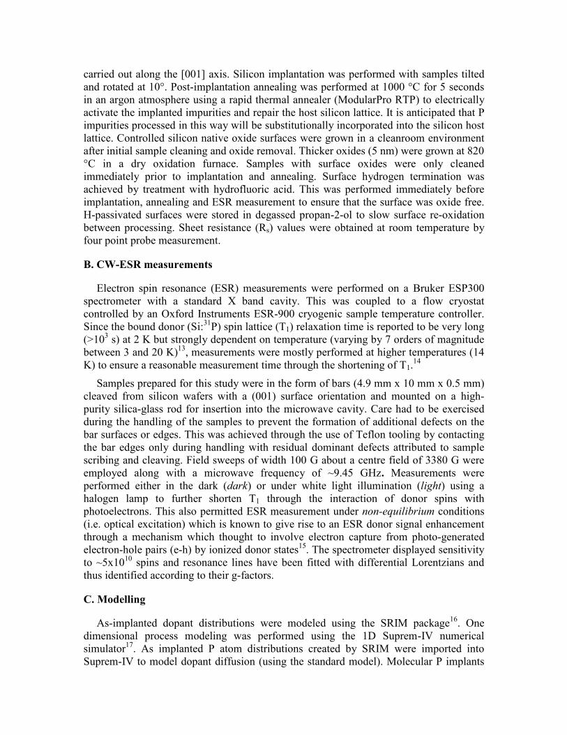
The one-dimensional, simulated substrate doping profiles for each of the annealed Pimplants studied are shown in Figs. 1(a) to (d). The implanted fluence, surfacetermination and estimated loss (%) to the surface oxide are all indicated. Channelling ofthe ion beam into hydrogen terminated silicon is also anticipated and modelled in (d).The simulations show the as-implanted dopant distribution added to a nominalbackground doping of the substrate (assumed to be around 1014 cm-3). Following thermalprocessing (RTA), the P is redistributed using a standard diffusion model and depicted inthe “annealed” plots. They show that the dopant diffusion range is expected to be smallunder these processing conditions which is important for nano-devices.
FIG. 1. Process simulations for the phosphorus ion implanted samples studied in this work. (A) 14 keVatomic P+ ions implanted (fluence = 4.1x1011 cm-2) through a 2 nm surface oxide, (B) 14 keV atomic P+
ions implanted (fluence = 2.1x1012 cm-2) through a 2 nm surface oxide, (C) 10 keV molecular P2+ ions
implanted (fluence = 8.0x1011 cm-2) through a 5 nm surface oxide and (D) 10 keV molecular P2+ ions
implanted (fluence = 2.0x1011 cm-2) through a H-passivated surface. The peak atomic P concentration hasnot been adjusted to correct for loss in the surface oxide.
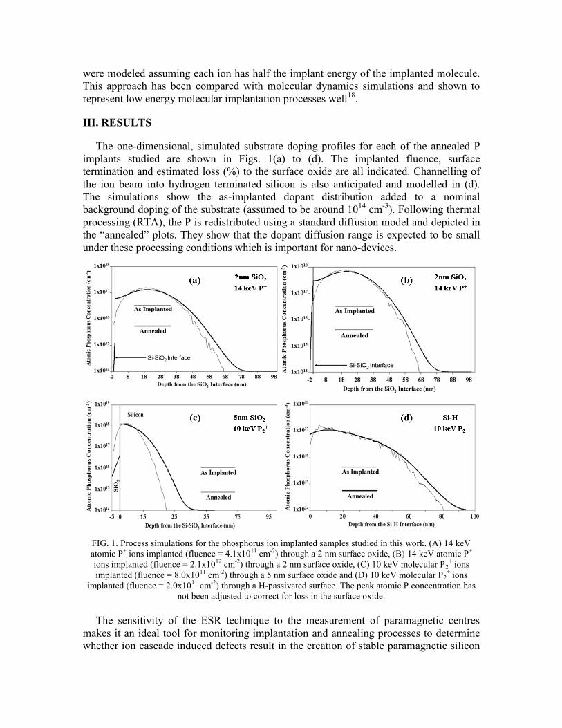
The sensitivity of the ESR technique to the measurement of paramagnetic centresmakes it an ideal tool for monitoring implantation and annealing processes to determinewhether ion cascade induced defects result in the creation of stable paramagnetic silicon

defects. For example, vacancy point defects (and their clusters) can assume positive,neutral and negative charge states which are identified as V+, V0 and V- with the V+ andV- states paramagnetic19. If the thermal repair of this damage is incomplete, electricallyactive point defects remain. Silicon ions are able to produce point, cluster and extendeddefects in silicon20 and have a similar damage profile to that of P ions but don’t introducedopant states making it a good choice for characterizing the effectiveness of theimplantation and thermal processes used in this work. Figure 2 shows ESR measurementsof high resistivity silicon which has been (a) untreated and (b) implanted with 14 keV Si-
ions (fluence = 1x1012 cm-2) followed by RTA processing. In both measurements, a broadfeature dominates the spectrum at 3364.3 G (g = 2.0055) corresponding to Pb (“danglingbond”) defects at the Si-SiO2 interface11, 12. The fitted peak area of the Pb resonance forthe implanted sample (b) is approximately double that of the untreated sample in (a). Anincrease in the Pb contribution to the spectrum would likely be associated with anincrease in the density of interfacial (electrical) trap states (Dits). This would be consistentwith the work of Peterström21 on unpassivated, phosphorus implanted (50 keV) oxideswhere Dits values were found to be sensitive to the ion implantation fluence, increasing byan order of magnitude over the range 5x10¹¹ to 4x10¹² P cm-2.
FIG. 2. Dark ESR measurements (14 K) of high resistivity silicon (ρ > 4 kΩ.cm) with a 2 nm native surfaceoxide (a) measured as supplied (untreated) and (b) implanted with 14 keV Si- ions to a fluence of 1x10¹²
cm-2 followed by thermal annealing. The Pb label with marker identifies the approximate location of the Pbdefect resonance feature. Plots have been offset.
The Pb states are known to be one of the most technologically important defects forMOS devices comprising trivalent silicon centres (•SiSi3)22. It should be noted thatmeasurements in this work include signals obtained from all surfaces of the sample, notjust the “top” implanted surface. This means that some of the interface signal originatesfrom damage introduced during substrate preparation and handling (e.g. scribing andcleaving). While it is clear that there is an increase in the Pb signal intensity associatedwith the silicon implant (compared to the untreated sample), no other paramagneticcentres are evident. This suggests that the processing conditions adopted in this work are

sufficient to remove all but the interface related defects. These interface defects areproblematic for nano-device applications however, it should be noted that surface oxidesare frequently removed and regrown or repaired by annealing in a hydrogen-containingambient to reduce the density of electrically active trap states. This process is thought toinvolve cracking centres which produce atomic hydrogen capable of passivating thedangling bond defects such as Pb centres and E’ defects23.
While ESR can be used to study P in silicon as electrically active (shallow) donorstates24, it can also be used to observe P related paramagnetic defects such as the Pvacancy pair in silicon (i.e. E-centre)25. Spectral identification of donor states is basedupon the observation of the hyperfine interaction of the donor electron with the magneticmoment of the 31P nucleus (I = ½, 100% natural abundance) giving rise to a spectraldoublet (~42 G splitting with g = 1.99875±0.00010)23. It is known that for Pconcentrations below 1016 cm-3, ESR measurements report only 2 hyperfine split linesarising from isolated donors26. For P concentrations around 1017 cm-3, evidence ofexchange coupling is expected as a central line feature (g = 1.99875). At concentrations(i) approaching and (ii) exceeding the metal-insulator (M-I) transition (~3.7x1018 cm-3)27,the hyperfine signal is replaced by (i) a dopant impurity band (DIB) (g = 1.99875) andfinally, (ii) a free (conduction band) electron line (g = 1.9995)28.
Figure 3 shows measurements from several 14 keV P+ implants prepared with fluencesranging from 4x1011 cm-2 up to 1x1013 cm-2 at which fluence, metallic donor states shouldform (i.e. [P]peak = 5x1018 cm-3). Sheet resistance values (Rs) are reported for preparations(a) and (b) which confirm high levels of dopant activation consistent with the annealed(simulated) dopant profiles. Substantial dopant segregation at the interface (i.e. P pileup)is not evident in these measurements as this would render P donors electrically inactiveresulting in higher sheet resistance values as has been reported previously8. The level ofdonor activation (electrical) obtained in this work was estimated by comparing themeasured Rs values with those calculated using the following empirical expression29
3.056267.0 1066.1105.91056.1 LnELnEKFRs (1)
where K is a constant with a value of 10108.5 ohm.cm-1.1 for donors, F is the implantfluence (ions/cm2) and E is the implant energy (keV). The activation values (%) for thetwo lowest fluence sample preparations, which demonstrate high implanted donor fluencerecoveries, are reported in Fig. 3.
The data in Fig. 3 shows clear signs of Pb defects, isolated and exchange coupled Pdonors and metallic (free electron) states in spectrum (c). These results are consistentwith the process simulations of Fig. 1 if we assume that the implanted ions are mostlyelectrically active, as suggested by the measured values of Rs, with distributionsdescribed by the annealed profiles. Comparing measurements in (a) and (b), we observevery similar donor resonance profiles with equivalent signal intensities along with weakexchange (central) resonance features which also have similar fitted areas. It is clear fromthese measurements that the donor hyperfine resonance signal intensity does not reflectthe order of magnitude difference in the implanted fluence between these samples. Inaddition, the exchange resonance (central) feature of spectrum (b) is considerably smaller
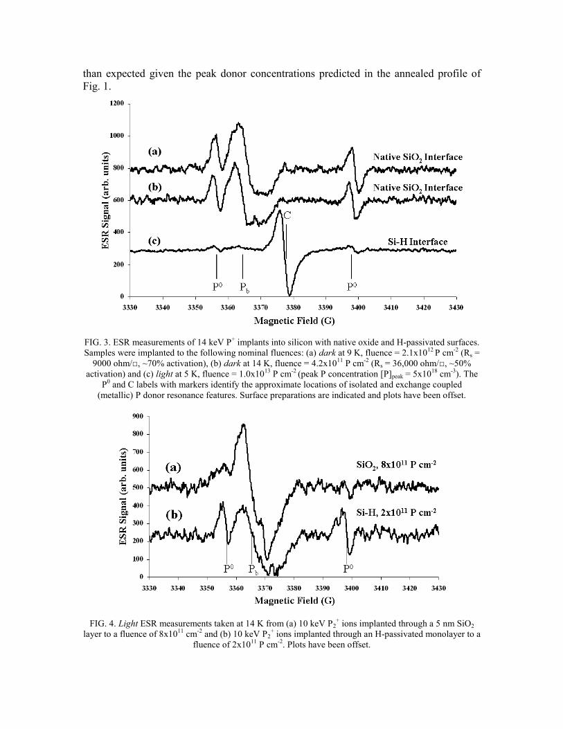
than expected given the peak donor concentrations predicted in the annealed profile ofFig. 1.
FIG. 3. ESR measurements of 14 keV P+ implants into silicon with native oxide and H-passivated surfaces.Samples were implanted to the following nominal fluences: (a) dark at 9 K, fluence = 2.1x10¹² P cm-2 (Rs =
9000 ohm/□, ~70% activation), (b) dark at 14 K, fluence = 4.2x10¹¹ P cm-2 (Rs = 36,000 ohm/□, ~50%activation) and (c) light at 5 K, fluence = 1.0x10¹³ P cm-2 (peak P concentration [P]peak = 5x1018 cm-3). The
P0 and C labels with markers identify the approximate locations of isolated and exchange coupled(metallic) P donor resonance features. Surface preparations are indicated and plots have been offset.
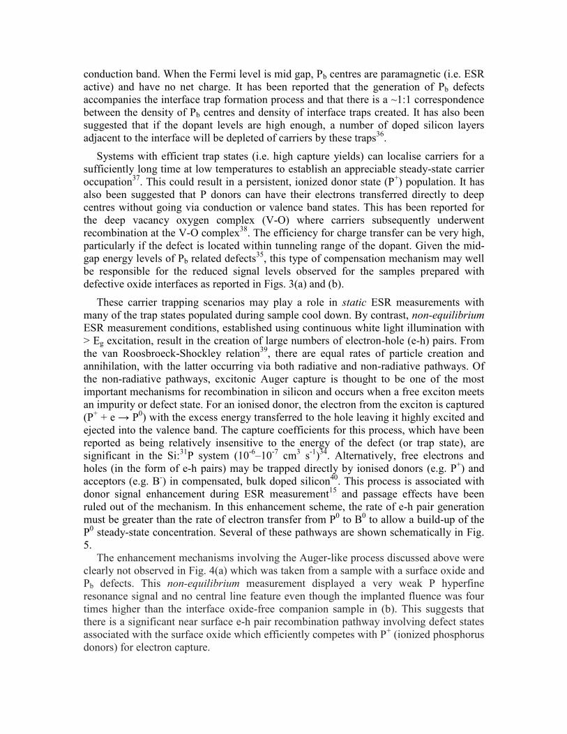
FIG. 4. Light ESR measurements taken at 14 K from (a) 10 keV P2+ ions implanted through a 5 nm SiO2
layer to a fluence of 8x1011 cm-2 and (b) 10 keV P2+ ions implanted through an H-passivated monolayer to a
fluence of 2x10¹¹ P cm-2. Plots have been offset.

The third spectrum reported in Fig. 3(c) results from an implanted fluence ([P]peak =5x1018 cm-3) greater than the M-I transition into a substrate with an H-passivated surface.This measurement shows a strong central line feature from a combination of exchangecoupled (including clustered, hyperfine collapsed) donors, conduction band states and asmaller doublet arising from uncoupled and exchange coupled donors. The absence of anSiO2 surface on this sample also results in a substantially reduced Pb defect resonancesignal in this spectrum.
The measurements reported in Fig. 4 arise from two samples which have beenimplanted with 10 keV molecular P2
+ ions through (a) a 5 nm SiO2 layer and (b) a H-passivated surface. Once again, the broad feature dominating the spectrum at 3365 Garises from Pb centres and is more intense for the sample with an SiO2 interface asexpected. In addition to this, a spectral doublet (i.e. hyperfine satellites) with ~42 Gsplitting centered at ~3377.5 G (g = 1.9987) is also evident and can be attributed to Pdonors. The measurements of Fig. 4 contrast the interface preparations and their impacton the donor resonance signal intensity. Both samples were implanted with 10 keV P2
+
ions at low fluences resulting in dopant profiles that are even closer to the interface thanthe measurements of Fig. 3. The first preparation (a) has a 5 nm surface oxide while thesecond (b) is H-passivated. While both spectra show evidence of Pb defect states withsimilar areas, the P resonance intensity is stronger in the presence of the H-passivatedsurface (~4 times the fitted area) even though the implanted fluence is four times lowerthan that of the oxide terminated surface. Ion losses to the oxide are not expected toexceed ~15 % and therefore, cannot account for the reduced signal intensity of thissample. In addition, these measurements were performed under white light illumination,the consequences of which are discussed below.
IV. DISCUSSION
Evaluating donor states near the Si-SiO2 interface presents a challenge for the ESRtechnique since the signal intensity is known to be dependent upon a number ofparameters including: the spin relaxation time (T1), frequency and amplitude of themodulating field, degree of dopant activation, dopant density and the intensity of themicrowave field. Furthermore, the dopant signal is affected by donor ionisation sinceonly the neutral charge, ground state of P donors (P0) contribute a resonance signal to theESR measurement (i.e. paramagnetic states)30. Donor ionization pathways include: holecapture from the valence band31 and electron emission to the conduction band (P0 → P+ +e), a process that can be driven thermally given the shallow nature of this impurity statein silicon. Carriers which have been emitted to the conduction band are subsequentlycaptured and retained by other centres (e.g. deep trap states) or may undergorecombination via a two step process whereby electrons and holes are capturedsuccessively as described by the Shockley-Read-Hall model32,33,34.
From the work of Lenahan et al 35, it is known that unoxidised silicon atoms at the Si-SiO2 interface give rise to silicon Pb and silica E’ defects. The Pb centres establishthemselves within silicon’s band gap where they can trap or deplete charge carriers andso effect the position of the Fermi energy. Specifically, Pb centres are known to beamphoteric; positively charged and diamagnetic when the Fermi level is near the valenceband and negatively charged and diamagnetic when the Fermi level is near the
conduction band. When the Fermi level is mid gap, Pb centres are paramagnetic (i.e. ESRactive) and have no net charge. It has been reported that the generation of Pb defectsaccompanies the interface trap formation process and that there is a ~1:1 correspondencebetween the density of Pb centres and density of interface traps created. It has also beensuggested that if the dopant levels are high enough, a number of doped silicon layersadjacent to the interface will be depleted of carriers by these traps36.
Systems with efficient trap states (i.e. high capture yields) can localise carriers for asufficiently long time at low temperatures to establish an appreciable steady-state carrieroccupation37. This could result in a persistent, ionized donor state (P+) population. It hasalso been suggested that P donors can have their electrons transferred directly to deepcentres without going via conduction or valence band states. This has been reported forthe deep vacancy oxygen complex (V-O) where carriers subsequently underwentrecombination at the V-O complex38. The efficiency for charge transfer can be very high,particularly if the defect is located within tunneling range of the dopant. Given the mid-gap energy levels of Pb related defects35, this type of compensation mechanism may wellbe responsible for the reduced signal levels observed for the samples prepared withdefective oxide interfaces as reported in Figs. 3(a) and (b).
These carrier trapping scenarios may play a role in static ESR measurements withmany of the trap states populated during sample cool down. By contrast, non-equilibriumESR measurement conditions, established using continuous white light illumination with> Eg excitation, result in the creation of large numbers of electron-hole (e-h) pairs. Fromthe van Roosbroeck-Shockley relation39, there are equal rates of particle creation andannihilation, with the latter occurring via both radiative and non-radiative pathways. Ofthe non-radiative pathways, excitonic Auger capture is thought to be one of the mostimportant mechanisms for recombination in silicon and occurs when a free exciton meetsan impurity or defect state. For an ionised donor, the electron from the exciton is captured(P+ + e → P0) with the excess energy transferred to the hole leaving it highly excited andejected into the valence band. The capture coefficients for this process, which have beenreported as being relatively insensitive to the energy of the defect (or trap state), aresignificant in the Si:31P system (10-6–10-7 cm3 s-1)34. Alternatively, free electrons andholes (in the form of e-h pairs) may be trapped directly by ionised donors (e.g. P+) andacceptors (e.g. B-) in compensated, bulk doped silicon40. This process is associated withdonor signal enhancement during ESR measurement15 and passage effects have beenruled out of the mechanism. In this enhancement scheme, the rate of e-h pair generationmust be greater than the rate of electron transfer from P0 to B0 to allow a build-up of theP0 steady-state concentration. Several of these pathways are shown schematically in Fig.5.
The enhancement mechanisms involving the Auger-like process discussed above wereclearly not observed in Fig. 4(a) which was taken from a sample with a surface oxide andPb defects. This non-equilibrium measurement displayed a very weak P hyperfineresonance signal and no central line feature even though the implanted fluence was fourtimes higher than the interface oxide-free companion sample in (b). This suggests thatthere is a significant near surface e-h pair recombination pathway involving defect statesassociated with the surface oxide which efficiently competes with P+ (ionized phosphorusdonors) for electron capture.

FIG. 5. Schematic band diagram of silicon showing several carrier emission, capture and recombinationpathways at donor and defect sites. A direct inter-centre charge transfer process is also depicted along with
a stylized interface model depicting P donor compensation.
The oxide companion sample shown in Fig. 4(b) has a H-passivated surface anddisplays significant P resonance signal intensity, especially given the very low implantenergy and fluence employed. The Si-H termination is often described as an ideal surfaceproviding an atomically flat and defect free (i.e. low disorder) interface with surface statedensities reported41 to be below 1010 cm-2. It comprises a hydrogen monolayer attached tooxide free silicon and is considered a good candidate for atomic scale electronic deviceswhere electrons are to be coupled to single atoms42. This measurement shows that byremoving the defective states associated with the SiO2 interface, a greater ESR Phyperfine signal to noise ratio can be obtained.
V. CONCLUSIONS
In this work, we have demonstrated the utility of CW-ESR as a tool for characterisingP ion implanted silicon where dopants are placed in close proximity (<50 nm) to a siliconinterface. Low energy, low fluence P implants were studied and shown to be electricallyactive, even when using ion energies as low as 5 keV and fluences around 1011 cm-2. Theimplantation/annealing process did not result in the introduction of new paramagneticcentres in the implanted region. Electrical measurements were used to estimate the levelsof donor activation which were found to be very high (≥ 50 %) for the 14 keV implantswhich is important for QC applications with single or few donor atoms. There was noevidence of transient enhanced diffusion or interfacial segregation for any of the 14 keVimplants as these dopant redistribution processes would have influenced both theelectrical and spectroscopic (ESR) measurements by changing the local donor statedensities.

Surprisingly, the ESR P hyperfine signal intensity could not be used to quantitativelyassess the degree of dopant activation in these preparations. The interfacial Si-SiO2defects, which can act as electrical traps, were found to cause the ionisation of donorstates as evidenced by a reduction in the intensity of the resonance signal in static ESRmeasurements. Non-equilibrium measurements also exhibited lower P hyperfineresonance signal levels when compared with companion samples prepared with an H-passivated surface. This suggests that the SiO2 interface defect states may be responsiblefor either enhanced e-h pair recombination or efficient inter-centre charge transfer.
ACKNOWLEDGEMENTS
This work was supported in part by the National Security Agency (NSA) under ArmyResearch Office (ARO) contract number W911NF-08-1-0527 and also by the AustralianResearch Council (ARC). Electronic materials engineering at the Australian National Universityis gratefully acknowledged for providing access to their implantation facilities.
1T. Shinada, S. Okamoto, T. Kobayashi, and I. Ohdomari, Nature 437, 1128 (2005).2B. E. Kane, Nature 393, 133 (1998).3A. Martinez, J. R. Barker, A. Svizhenko, M. P. Anantram, and A. Asenov, IEEE Trans.
Nanotechnology 6, 438 (2007).4S. Fatima, J. Wong-Leung, J. FitzGerald, and C. Jagadish, Appl. Phys. Lett. 72, 3044
(1998).5P. A. Stolk, H.-J. Gossmann, D. J. Eaglesham, D. C. Jacobson, C. S. Rafferty, G. H.
Gilmer, M. Jaraı´z, J. M. Poate, H. S. Luftman, and T. E. Haynes, J. Appl. Phys. 81,6031 (1997).
6S. Ruffell, I. V. Mitchell, and P. J. Simpson, J. Appl. Phys. 97, 123518 (2005).7H.-H. Vuong, C. S. Rafferty, S. A. Eshraghi, J. Ning, J. R. McMacken, S. Chaudhry, J.
McKinley, and F. A. Stevie, J. Vac. Sci. Technol. B 18, 428 (2000).8G. A. Sai-Halasz, K. T. Short, and J. S. Williams, IEEE Electron Device Lett. 6, 285
(1985).9D. N. Jamieson, C. Yang, T. Hopf, S. M. Hearne, C. I. Pakes, and S. Prawer, M. Mitic,
E. Gauja, S. E. Andresen, F. E. Hudson, A. S. Dzurak, and R. G. Clark Appl. Phys. Lett.86, 202101 (2005);
10T. Schenkel,_ J. A. Liddle, A. Persaud, A. M. Tyryshkin, S. A. Lyon, R. de Sousa, K.B. Whaley, J. Bokor, J. Shangkuan, and I. Chakarov, Appl. Phys. Lett. 88, 112101(2006).
11Y. Nishi, Jpn. J. Appl. Phys. 10, 52 (1971).12Y. Nishi, T. Tanaka, and A. Ohwada, Jpn. J. Appl. Phys. 11, 85 (1972).13G. Feher, and E. Gere, Phys. Rev. 114, 1245 (1959).14E. Abe, K. Itoh, J. Isoya, and S. Yamasaki, Phys. Rev. B 70, 033204 (2004).15 A. Honig, and R. Levitt, Phys. Rev. Lett. 5, 93 (1960).

16J.F. Ziegler, J.P. Biersack, and U. Littmark, “SRIM - The Stopping and Range of Ionsin Solids,” Pergamon Press, New York, (1985).
17M. E. Law, C. S. Rafferty, and R. W. Dutton, “SUPREM-IV User’s Manual” StanfordUniversity, Stanford, CA (1988).
18H.F. Wilson, S. Prawer, P.G. Spizzirri, N. Stavrias, D. N. Jamieson, and D.R.McKenzie, Nucl. Instrum. Methods Phys. Res., Sect. B 251, 395 (2006).
19P. M. Fahey, P. B. Griffin, and J. D. Plummer, Rev. Mod. Phys. 61, 289 (1989).20J. L. Benton, S. Libertino, P. Kringhøj, D. J. Eaglesham, J. M. Poate, and S. Coffa, J.
Appl. Phys. 82, 120 (1997).21S. Peterström, Appl. Phys. Lett. 63, 672 (1993).22Stirling, A. Pasquarello, J.-C. Charlier, and R. Car, Phys. Rev. Lett. 85, 2773 (2000).23R. E. Stahlbush, A. H. Edwards, D. L. Griscom, and B. J. Mrstik, J. Appl. Phys. 73, 658
(1993).24G. Feher, Phys. Rev. 114, 1219 (1959).25M. G. Ganchenkova, A. Yu. Kuznetsov, and R. M. Nieminen, Phys. Rev. B 70, 115204
(2004).26D. New, Phys. Rev. B 32, 2419 (1985).27T. F. Rosenbaum, R. F. Milligan, M. A. Paalanen, G. A. Thomas, R. N. Bhatt, and W.
Lin, Phys. Rev. B 27, 7509 (1983).28C. F. Young, E. H. Poindexter, G. J. Gerardi, W. L. Warren, and D. J. Keeble, Phys.
Rev. B 55, 16245 (1997).29K. H. Nicholas, Radiat. Eff. Defects Solids 28, 177 (1976).30C. Kisielowski, J. Palm, B. Bollig, and H. Alexander, Phys. Rev. B 44, 1588 (1991).31M. Keleverman, H. G. Grimmeiss, A. Litwin, and E. Janzén, Phys. Rev. B 31, 3659
(1985).32R. N. Hall, Phys. Rev. 87, 387 (1952).33W. Shockley, and W. T. Read, Phys. Rev. 87, 835 (1952).34A. Hangleiter, Phys. Rev. B 37, 2594 (1988).35P. M. Lenahan, and P. V. Dressendorfer, Appl. Phys. Lett. 44, 96 (1984).36J. J. Boland, Nature 439, 671 (2006).37W.M. Chen, B. Monemar, E. Janzén, and J. L. Lindström, Phys. Rev. Lett. 67, 1914
(1991).38A. J. R. deKock, J. Electrochem. Soc. 118, 1851 (1971).39W. van Roosbroeck, and W. Shockley, Phys. Rev. 94, 1558 (1954).40T. Igo, Jap. J. Appl. Phys. 4, 523 (1965).
41B. R. Weinberger, H. W. Deckman, E. Yablonovitch, T. Gmitter, W. Kobasz, andS.Garoff, J. Vac. Sci. Technol. A 3, 887 (1985).
42K. Eng, R. N. McFarland, and B. E. Kane, Appl. Phys. Lett. 87, 052106 (2005).
Copyright © 2022 FDOKUMEN


![Diffusion of 18 elements implanted into thermally grown SiO[sub 2]](https://static.fdokumen.com/doc/165x107/6335afedcd4bf2402c0b3112/diffusion-of-18-elements-implanted-into-thermally-grown-siosub-2.jpg)