Journal Seema 16dec12 esr
10
*Corresponding Author www.ijesr.org 2094 IJESR/Dec 2012/ Volume-2/Issue-12/Article No-16/2094-2103 ISSN 2277-2685 International Journal of Engineering & Science Research 8 BIT PIPE LINE ANALOG TO DIGITAL CONVERTER Seema Kanathe* 1 , Amit Rajput 1 1 Department of Electronics & Communication, RITS, Bhopal, MP, India. ABSRACT This Paper present a 8 bit ADC is designed for the implementation of pipeline ADC. To design this ADC we used TIQ comparator that reduced the power consumption and area. The sample and hold circuit have high Sampling rate. This Design is implemented and verified on the synopsys CosmosSE & Cscope in 0.35µm Technology Keywords : Pipe line ADC ,S/H circuit, DAC, TIQ comparator. INTRODUCTION The pipeline ADC architecture as shown in Figure 1 utilizes a sample-and-hold (S/H) in each stage to increase the throughput. Each stage consists of an S/H, an N-bit flash ADC, a reconstruction DAC, a subtractor, and a residue amplifier. Pipelined converters are more commonly used to realize high conversion rates since they provide effective signal bandwidths equal of 10-100 MHz (sample rates of 20-200 MHz). The conversion mechanism is similar to that of sub-ranging conversion in each stage. Now the amplified residue is sampled by the next S/H, instead of being fed to the following stage. All the N-bit digital outputs emerging from the quantizer are combined as a final code by using the proper number of delay registers and digital error correction logic Figure 1: pipeline ADC SINGLE STAGES ADC DESIGN As the through put should be as fast as of flash ADC, so each stage of the pipeline ADC is inherited form flash architecture. The resolution of each stage will decide how many comparators are required, what will be the latency of the system, what kind of DAC architecture has to be incorporated, need of fast encoding circuitry. For example, if we choose 3 bits per stage, than for 7 bit pipeline ADC, there will be total three stages one will comprises of one bit ADC and remaining will have 3 bit ADC architecture, thus the total number of comparator required are 35(2 3 +2 3 +1-2) also it will require two (2 bit) and one (1 bit) DAC. Since the selected architecture comprises of one bit ADC this only one comparator is required and total number of comparator will be 7, drastically reduced This is the reason,
-
Upload
independent -
Category
Documents
-
view
2 -
download
0
Transcript of Journal Seema 16dec12 esr
*Corresponding Author www.ijesr.org 2094
IJESR/Dec 2012/ Volume-2/Issue-12/Article No-16/2094-2103 ISSN 2277-2685
International Journal of Engineering & Science Research
8 BIT PIPE LINE ANALOG TO DIGITAL CONVERTER
Seema Kanathe*1, Amit Rajput
1
1Department of Electronics & Communication, RITS, Bhopal, MP, India.
ABSRACT
This Paper present a 8 bit ADC is designed for the implementation of pipeline ADC. To
design this ADC we used TIQ comparator that reduced the power consumption and area. The
sample and hold circuit have high Sampling rate. This Design is implemented and verified on
the synopsys CosmosSE & Cscope in 0.35µm Technology
Keywords : Pipe line ADC ,S/H circuit, DAC, TIQ comparator.
INTRODUCTION
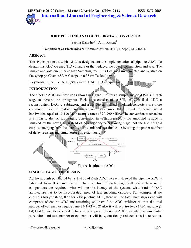
The pipeline ADC architecture as shown in Figure 1 utilizes a sample-and-hold (S/H) in each
stage to increase the throughput. Each stage consists of an S/H, an N-bit flash ADC, a
reconstruction DAC, a subtractor, and a residue amplifier. Pipelined converters are more
commonly used to realize high conversion rates since they provide effective signal
bandwidths equal of 10-100 MHz (sample rates of 20-200 MHz). The conversion mechanism
is similar to that of sub-ranging conversion in each stage. Now the amplified residue is
sampled by the next S/H, instead of being fed to the following stage. All the N-bit digital
outputs emerging from the quantizer are combined as a final code by using the proper number
of delay registers and digital error correction logic
Figure 1: pipeline ADC
SINGLE STAGES ADC DESIGN
As the through put should be as fast as of flash ADC, so each stage of the pipeline ADC is
inherited form flash architecture. The resolution of each stage will decide how many
comparators are required, what will be the latency of the system, what kind of DAC
architecture has to be incorporated, need of fast encoding circuitry. For example, if we
choose 3 bits per stage, than for 7 bit pipeline ADC, there will be total three stages one will
comprises of one bit ADC and remaining will have 3 bit ADC architecture, thus the total
number of comparator required are 35(23+2
3+1-2) also it will require two (2 bit) and one (1
bit) DAC. Since the selected architecture comprises of one bit ADC this only one comparator
is required and total number of comparator will be 7, drastically reduced This is the reason,
IJESR/Dec 2012/ Volume-2/Issue-12/Article No-16/2094-2103 ISSN 2277-2685
Copyright © 2012 Published by IJESR. All rights reserved 2095
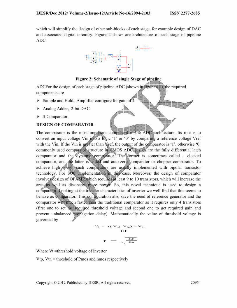
which will simplify the design of other sub-blocks of each stage, for example design of DAC
and associated digital circuitry. Figure 2 shows are architecture of each stage of pipeline
ADC.
Figure 2: Schematic of single Stage of pipeline
ADCFor the design of each stage of pipeline ADC (shown in figure 4.1), the required
components are
� Sample and Hold., Amplifier configure for gain of 4.
� Analog Adder, 2-bit DAC
� 3-Comparator.
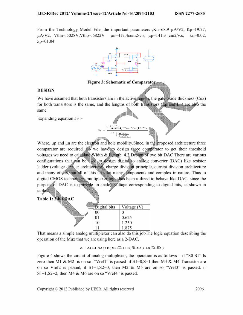
DESIGN OF COMPARATOR
The comparator is the most important component in the ADC architecture. Its role is to
convert an input voltage Vin into a logic ‘1’ or ‘0’ by comparing a reference voltage Vref
with the Vin. If the Vin is greater than Vref, the output of the comparator is ‘1’, otherwise ‘0’
commonly used comparator structure in CMOS ADC design are the fully differential latch
comparator and the dynamic comparator. The former is sometimes called a clocked
comparator, and the latter is called and auto-zero comparator or chopper comparator. To
achieve high speed, such comparators are usually implemented with bipolar transistor
technology. For SOC implementation in this case, Moreover, the design of comparator
involves design of OPAMP which requires at least 9 to 10 transistors, which will increase the
area as well as dissipates more power. So, this novel technique is used to design a
comparator. Looking at the transfer characteristics of inverter we well find that this seems to
behave as comparator. This configuration also save the need of reference generator and the
comparator will much faster than the traditional comparator as it requires only 4 transistors
(first one to set the required threshold voltage and second one to get required gain and
prevent unbalanced propagation delay). Mathematically the value of threshold voltage is
governed by-
Where Vt =threshold voltage of inverter
Vtp, Vtn = threshold of Pmos and nmos respectively
IJESR/Dec 2012/ Volume-2/Issue-12/Article No-16/2094-2103 ISSN 2277-2685
Copyright © 2012 Published by IJESR. All rights reserved 2096
From the Technology Model File, the important parameters ,Kn=68.9 µA/V2, Kp=19.77,
µA/V2, Vthn=.5028V,Vthp=.6822V µn=417.4com2/v.s, µp=141.3 cm2/v.s, λn=0.02,
λp=01.04
Figure 3: Schematic of Comparator
DESIGN
We have assumed that both transistors are in the active region, the gate oxide thickness (Cox)
for both transistors is the same, and the lengths of both transistors (Lp and Ln) are also the
same.
Expanding equation 531-
Where, µp and µn are the electron and hole mobility.Since, in the proposed architecture three
comparator are required. So we have to design three comparator to get their threshold
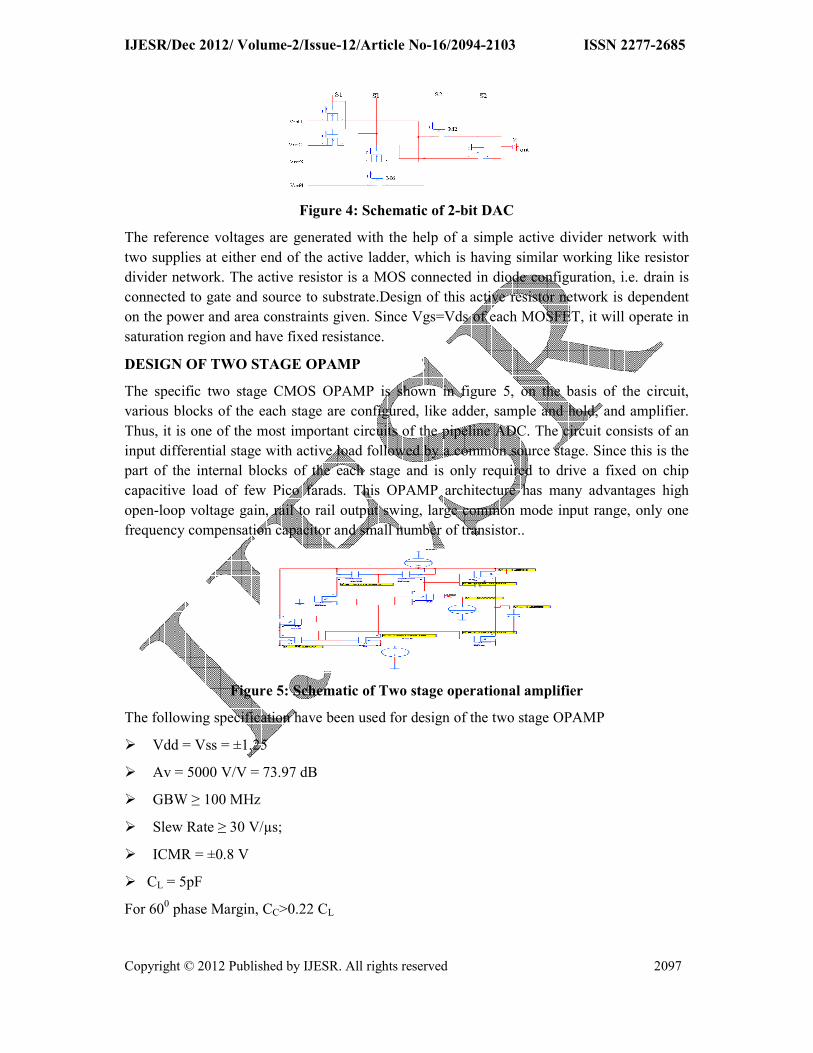
voltages we need to calculate Width & Length. 4.3 Design of two bit DAC There are various
configurations that can be used to design digital to analog converter (DAC) like resistor
ladder (voltage divider architecture), charge division principle, current division architecture
and many others, but all of this uses lot many components and complex in nature. Thus to
digital CMOS technology, multiplexer logic has been utilized to behave like DAC, since the
purpose of DAC is to provide an analog voltage corresponding to digital bits, as shown in
table 1.
Table 1: 2-bit DAC
Digital bits Voltage (V)
00
01
10
11
0
0.625
1.250
1.875
That means a simple analog multiplexer can also do this jobThe logic equation describing the
operation of the Mux that we are using here as a 2-DAC.
Figure 4 shows the circuit of analog multiplexer, the operation is as follows – if “S0 S1” Is
zero then M1 & M2 is on so “Vref1” is passed .if S1=0,S=1,then M3 & M4 Transistor are
on so Vref2 is passed, if S1=1,S2=0, then M2 & M5 are on so “Vref3” is passed. if
S1=1,S2=2, then M4 & M6 are on so “Vref4” is passed.
IJESR/Dec 2012/ Volume-2/Issue-12/Article No-16/2094-2103 ISSN 2277-2685
Copyright © 2012 Published by IJESR. All rights reserved 2097
Figure 4: Schematic of 2-bit DAC
The reference voltages are generated with the help of a simple active divider network with
two supplies at either end of the active ladder, which is having similar working like resistor
divider network. The active resistor is a MOS connected in diode configuration, i.e. drain is
connected to gate and source to substrate.Design of this active resistor network is dependent
on the power and area constraints given. Since Vgs=Vds of each MOSFET, it will operate in
saturation region and have fixed resistance.
DESIGN OF TWO STAGE OPAMP
The specific two stage CMOS OPAMP is shown in figure 5, on the basis of the circuit,
various blocks of the each stage are configured, like adder, sample and hold, and amplifier.
Thus, it is one of the most important circuits of the pipeline ADC. The circuit consists of an
input differential stage with active load followed by a common source stage. Since this is the
part of the internal blocks of the each stage and is only required to drive a fixed on chip
capacitive load of few Pico farads. This OPAMP architecture has many advantages high
open-loop voltage gain, rail to rail output swing, large common mode input range, only one
frequency compensation capacitor and small number of transistor..
Figure 5: Schematic of Two stage operational amplifier
The following specification have been used for design of the two stage OPAMP
� Vdd = Vss = ±1.25
� Av = 5000 V/V = 73.97 dB
� GBW ≥ 100 MHz
� Slew Rate ≥ 30 V/µs;
� ICMR = ±0.8 V
� CL = 5pF
For 600 phase Margin, CC>0.22 CL
IJESR/Dec 2012/ Volume-2/Issue
Copyright © 2012 Published by IJESR
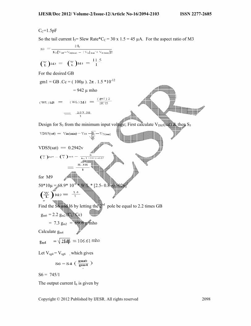
CC=1.5pF
So the tail current I5= Slew Rate*C
For the desired GB
gm1 = GB .Cc = ( 100µ ). 2π . 1.5 *10
= 942 µ mho
Design for S5 from the minimum input voltage; First calculate V
VDS5(sat) == 0.2942v
for M9
50*10µ = 68.9* 10-6
* W/L * [2.5
Find the S6 and I6 by letting the 2
gm6 = 2.2 gm2 (CL/ Cc)
= 7.3 gm2 = 6908 µ mho
Calculate gm4
Let Vsg4 = Vsg6 , which gives
S6 = 745/1
The output current I6 is given by
2/Issue-12/Article No-16/2094-2103 ISSN 2277
yright © 2012 Published by IJESR. All rights reserved
= Slew Rate*CC = 30 x 1.5 = 45 µA. For the aspect ratio of M3
gm1 = GB .Cc = ( 100µ ). 2π . 1.5 *10-12
from the minimum input voltage; First calculate VDS5(sat) & then S
[2.5- 0.8 -0.5028]2
Find the S6 and I6 by letting the 2nd
pole be equal to 2.2 times GB
is given by
ISSN 2277-2685
2098
= 30 x 1.5 = 45 µA. For the aspect ratio of M3
(sat) & then S5
IJESR/Dec 2012/ Volume-2/Issue-12/Article No-16/2094-2103 ISSN 2277-2685
Copyright © 2012 Published by IJESR. All rights reserved 2099
The aspect ratio S7 is given by
S7 = S5. ( I6 / I5 )
= 270 / 1
So the design results of each transistor are given in table 2.
Table 2: MOS Sizes for Operational Amplifier
Index of MOS W/L
M1, M2
M3, M4
M5
M6
M7
M8
M9
258/1
11.5/1
8.3/1
745/1
270/1
8.3/1
1.4/6
SAMPLE & HOLD CIRCUIT
The basic elements of a sample & hold circuit are a storage element and a switch. These are
generally implemented by using a capacitor (for storing) and a MOSFET for sampling
through a CLK control signal. But as a single MOSFET may not pass the positive and
negative voltages in the same way, it is replaced with a Tx gate. The sizing of this Tx gate
will decide the ON resistance of the switch and this will decide the RC time constant for
charging the capacitor. Two buffers are used to avoid the loading on the source when
sampling, and to avoid the charge discharge through the capacitor when it is in the hold
mode. These buffers are implemented with an OPAMP in a voltage follower configuration as
shown in the figure 6.
Figure 6: Schematic of Sample & hold Circuit
The sampling CLK is given to the CONTr of the Tx gate. When the CLK is high the input
signal is sampled through the 1st buffer and the capacitor is charged to the input level. When
once the CLK goes to LOW, then the path from the input is open circuited and the sampled
voltage is maintained constant and given to the preceding block for conversion. For a better
sampling the sampling rate should be at least 2 times to that of the input signal frequency.
DESIGN OF ANALOG ADDER
While designing pipeline ADC, an idea comes to the mind, how an analog circuit will
sometimes acts as adder and sometime act as subtractor, this query of the mind gets cleared
by utilizing the concept of multiplexer, for example sometimes a positive potential is applied

IJESR/Dec 2012/ Volume-2/Issue-12/Article No-16/2094-2103 ISSN 2277-2685
Copyright © 2012 Published by IJESR. All rights reserved 2100
and sometimes negative, thus the same circuit gives summation as well as difference results.
Considering the above situation shown in figure 7.
Figure 7: schematic of Analog Adder
The difference amplifier configuration could not fit in to design as the OPAMP utilized for
this configuration does not have same input impedance on both of the terminal, thus the
second configuration analog adder is chosen in the proposed design. The configuration has
the advantage, as both of the input voltage are applied to same terminal and would not suffer
the effect of loading.
DESIGN OF D FLIP-FLOP
Flip-flops are the traditional storage elements used to realize synchronous logic circuits. They
save the state of the machine from one clock cycle to the next. They are also used to break up
any feedback loops around a cyclic logic circuit to prevent the logic from having race
condition or oscillations. It is one of the necessary elements in the pipeline ADC, the main
point to raise here is that, it is used as delay element which will synchronize the bits of the all
stages, by configuring the flip-flop as varying length shift register, it will synchronize the
output of pipeline ADC
Figure 8: Schematic of D-flipflop
SIMULATION RESULTS & DISCUSSION
The design of 8-bit pipeline ADC has been carried out in tsmc035 (Taiwan semiconductor
manufacturing corporation) technology, but the design of pipeline ADC gets limited to 8-bit.
This is a 0.35 µm SCN3M_SUBM (lambda =.20), thick oxide process technology. The
supply voltage is bipolar +/- 1.25 (2.5v) the tool used for the design are synopsys’s cosmosSE
for schematic, H-spice for Simulation, cscope for waveform viewing.The sub modules
designed above verified by using the SPICE command for DC,AC, and Transient analysis.
IJESR/Dec 2012/ Volume-2/Issue
Copyright © 2012 Published by IJESR
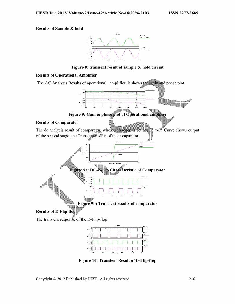
Results of Sample & hold
Figure 8: transient resu
Results of Operational Amplifier
The AC Analysis Results of operational amplifier, it shows the gain and phase plot
Figure 9: Gain & phase plot of Operational amplifier
Results of Comparator
The dc analysis result of comparator, whose reference is set at1.25 volt. Curve shows output
of the second stage .the Transient results of the comparator.
Figure 9a: DC
Figure 9
Results of D-Flip flop
The transient response of the D-Flip
Figure 10:
2/Issue-12/Article No-16/2094-2103 ISSN 2277
yright © 2012 Published by IJESR. All rights reserved
transient result of sample & hold circuit
Results of Operational Amplifier
The AC Analysis Results of operational amplifier, it shows the gain and phase plot
Gain & phase plot of Operational amplifier
comparator, whose reference is set at1.25 volt. Curve shows output
of the second stage .the Transient results of the comparator.
DC-sweep Characteristic of Comparator
Figure 9b: Transient results of comparator
Flip-flop
10: Transient Result of D-Flip-flop
ISSN 2277-2685
2101
The AC Analysis Results of operational amplifier, it shows the gain and phase plot
comparator, whose reference is set at1.25 volt. Curve shows output
IJESR/Dec 2012/ Volume-2/Issue-12/Article No-16/2094-2103 ISSN 2277-2685
Copyright © 2012 Published by IJESR. All rights reserved 2102
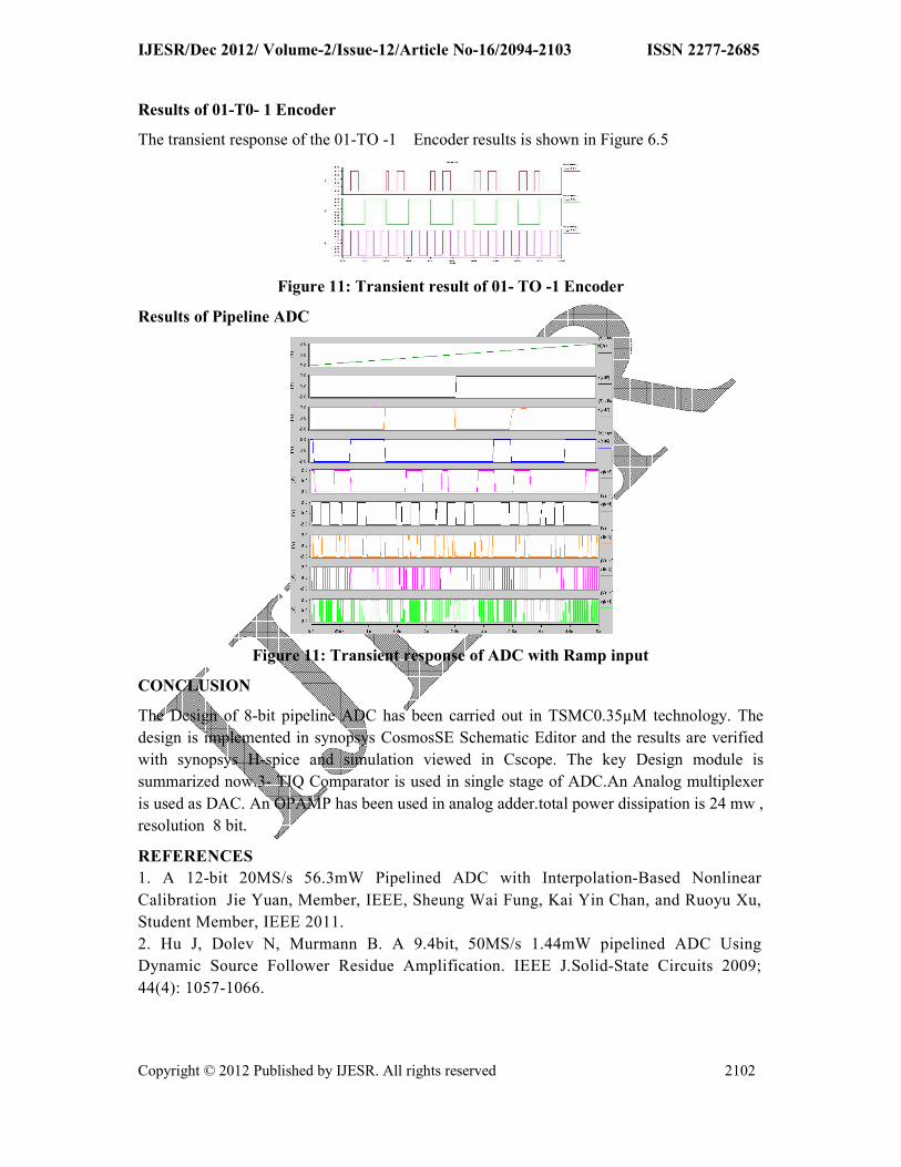
Results of 01-T0- 1 Encoder
The transient response of the 01-TO -1 Encoder results is shown in Figure 6.5
Figure 11: Transient result of 01- TO -1 Encoder
Results of Pipeline ADC
Figure 11: Transient response of ADC with Ramp input
CONCLUSION
The Design of 8-bit pipeline ADC has been carried out in TSMC0.35µM technology. The
design is implemented in synopsys CosmosSE Schematic Editor and the results are verified
with synopsys H-spice and simulation viewed in Cscope. The key Design module is
summarized now.3- TIQ Comparator is used in single stage of ADC.An Analog multiplexer
is used as DAC. An OPAMP has been used in analog adder.total power dissipation is 24 mw ,
resolution 8 bit.
REFERENCES
1. A 12-bit 20MS/s 56.3mW Pipelined ADC with Interpolation-Based Nonlinear
Calibration Jie Yuan, Member, IEEE, Sheung Wai Fung, Kai Yin Chan, and Ruoyu Xu,
Student Member, IEEE 2011.
2. Hu J, Dolev N, Murmann B. A 9.4bit, 50MS/s 1.44mW pipelined ADC Using
Dynamic Source Follower Residue Amplification. IEEE J.Solid-State Circuits 2009;
44(4): 1057-1066.
IJESR/Dec 2012/ Volume-2/Issue-12/Article No-16/2094-2103 ISSN 2277-2685
Copyright © 2012 Published by IJESR. All rights reserved 2103
3. Centurelli F, Monsurro P, Trifiletti A. Behavioral modeling for calibration of pipeline
analog-to-digital converters. IEEE Trans. Circuits and Systems I: Regular Papers 2010;
57: 1255-1264.
4. Peng B, Li H, Lee SC, Lin P, Chiu Y. A virtual-ADC digital background calibration
technique for multistage A/D converter. IEEE Trans. Circuits and Systems II: Express
Briefs 2010; 57: 853-857.
5. Lee B, Tsang R. A 10-bit 50MS/s Pipelined ADC With Capacitor- Sharing and
Variable-gm OPAMP. IEEE J. Solid-State Circuits 2009; 44(3): 883-890
6. Peng B, Li H, Lee SC, Lin P, Chiu Y. A virtual-ADC digital background calibration
technique for multistage A/D converter. IEEE Trans. Circuits and Systems II: Express
Briefs 2010; 57: 853-857.
7. Shu Y, Song B. A 15-bit Linear 20-MS/s Pipelined ADC Digitally Calibrated With
Signal-Dependent Dithering. IEEE J. Solid-State Circuits 2008; 43(2): 342-350.