
Enhancing the photocatalytic efficiency of sprayed ZnO thin filmsthrough double doping (Sn + F) and...
8
Applied Surface Science 321 (2014) 310–317 Contents lists available at ScienceDirect Applied Surface Science journal h om epa ge: www.elsevier.com/locate/apsusc Enhancing the photocatalytic efficiency of sprayed ZnO thin films through double doping (Sn + F) and annealing under different ambiences K. Ravichandran a,∗ , R. Mohan a , B. Sakthivel a , S. Varadharajaperumal b , P. Devendran c , T. Alagesan c , K. Pandian d a Post Graduate & Research Department of Physics, AVVM Sri Pushpam College (Autonomous), Poondi, Thanjavur 613 503, Tamil Nadu, India b Center for Nano Science and Engineering, Indian Institute of Science, Bangalore 560 012, Karnataka, India c Department of Physics, Presidency College, Chennai 600 005, India d Department of Inorganic Chemistry, University of Madras, Guindy Campus, Chennai 600 025, India a r t i c l e i n f o Article history: Received 3 August 2014 Received in revised form 29 September 2014 Accepted 3 October 2014 Available online 12 October 2014 Keywords: Doubly doped ZnO thin films Annealing XPS HR-TEM Photocatalytic activity a b s t r a c t Doubly (Sn + F) doped zinc oxide (ZnO:Sn:F) thin films were deposited onto glass substrates using a simplified spray pyrolysis technique. The deposited films were annealed at 400 ◦ C under two different ambiences (air and vacuum) for 2 h. The photocatalytic activity of these films was assessed through pho- tocatalytic decolorization kinetics of Methylene Blue (MB) dye and the decolorization efficiency of the annealed films was compared with that of their as-deposited counterpart. The photocatalytic studies reveal that the ZnO:Sn:F films annealed under vacuum environment exhibits better photocatalytic effi- ciency when compared with both air annealed and as-deposited films. The SEM and TEM images depict that the surface of each of the films has an overlayer comprising of nanobars formed on a bottom layer, having spherical grains. The studies show that the diameter of the nanobars plays crucial role in enhancing the photocatalytic activity of the ZnO:Sn:F films. The structural, optical and electrical studies substantiate the discussions on the photocatalytic ability of the deposited films. © 2014 Elsevier B.V. All rights reserved. 1. Introduction With the fast development of dye industry, dye effluents become a major source of water pollution which are difficult and expensive to eliminate using conventional water treatment technologies [1,2]. Therefore, development of cost-effective photocatalysts to control water pollution assumes top priority in contemporary research. In recent years, semiconductor photocatalysts have attracted increasing attention and among the various semiconductor oxide photocatalysts, ZnO looks very promising because of its electric and photonic properties, and oxidation resistance [3]. In addition, it is inexpensive, more environmental friendly, chemically stable and in some cases it has a higher photocatalytic activity than TiO 2 , which is by far the most widely used metal oxide photocatalyst [4,5]. When ZnO is irradiated with light having energy equal to or greater than ∗ Corresponding author at: Post Graduate & Research Department of Physics, AVVM Sri Pushpam College (Autonomous), Poondi, Thanjavur 613 503, Tamil Nadu, India. Tel.: +91 4362 278602; fax: +91 4374 239328; mobile: +91 9443524180. E-mail address: [email protected] (K. Ravichandran). its band gap (E g = 3.37 eV), electron–hole pairs are generated which is generally followed by the recombination process. But, to increase the photocatalytic efficiency, suppression of the recombination of photogenerated electron–hole pairs is essential [6,7] which can be achieved mainly via creation of surface oxygen vacancies [8] and certain extrinsic defects. In this respect, we have doped Sn and F simultaneously with ZnO in order to enhance the surface defects. It is a well known fact that the doping is an effective route to slowdown the recom- bination process [9]. To enhance the photocatalytic activity of ZnO further, post-deposition annealing under two different ambiences is also attempted as heat treatment has significant impact on the concentration of oxygen vacancies in the sample. It is worth mentioning here that, in the present study, Sn and F doped ZnO (ZnO:Sn:F) films have been prepared from a starting solution having only 10 mL of solvent volume which is expected to promote more defects like interstitials and vacancies due to higher spray flux density [10]. Moreover, to reduce the production cost, a simplified spray pyrolysis technique using a perfume atomizer has been employed. The employment of this spray pyrolysis tech- nique facilitates the production of low cost [11] ZnO films with large http://dx.doi.org/10.1016/j.apsusc.2014.10.023 0169-4332/© 2014 Elsevier B.V. All rights reserved.
-
Upload
kalsaslingam -
Category
Documents
-
view
2 -
download
0
Transcript of Enhancing the photocatalytic efficiency of sprayed ZnO thin filmsthrough double doping (Sn + F) and...
Eta
KPa
b
c
d
a
ARR2AA
KDAXHP
1
atTw
ippisbZ
AI
h0
Applied Surface Science 321 (2014) 310–317
Contents lists available at ScienceDirect
Applied Surface Science
journa l h om epa ge: www.elsev ier .com/ locate /apsusc
nhancing the photocatalytic efficiency of sprayed ZnO thin filmshrough double doping (Sn + F) and annealing under differentmbiences
. Ravichandrana,∗, R. Mohana, B. Sakthivela, S. Varadharajaperumalb,. Devendranc, T. Alagesanc, K. Pandiand
Post Graduate & Research Department of Physics, AVVM Sri Pushpam College (Autonomous), Poondi, Thanjavur 613 503, Tamil Nadu, IndiaCenter for Nano Science and Engineering, Indian Institute of Science, Bangalore 560 012, Karnataka, IndiaDepartment of Physics, Presidency College, Chennai 600 005, IndiaDepartment of Inorganic Chemistry, University of Madras, Guindy Campus, Chennai 600 025, India
r t i c l e i n f o
rticle history:eceived 3 August 2014eceived in revised form9 September 2014ccepted 3 October 2014vailable online 12 October 2014
a b s t r a c t
Doubly (Sn + F) doped zinc oxide (ZnO:Sn:F) thin films were deposited onto glass substrates using asimplified spray pyrolysis technique. The deposited films were annealed at 400 ◦C under two differentambiences (air and vacuum) for 2 h. The photocatalytic activity of these films was assessed through pho-tocatalytic decolorization kinetics of Methylene Blue (MB) dye and the decolorization efficiency of theannealed films was compared with that of their as-deposited counterpart. The photocatalytic studiesreveal that the ZnO:Sn:F films annealed under vacuum environment exhibits better photocatalytic effi-
eywords:oubly doped ZnO thin filmsnnealingPSR-TEMhotocatalytic activity
ciency when compared with both air annealed and as-deposited films. The SEM and TEM images depictthat the surface of each of the films has an overlayer comprising of nanobars formed on a bottom layer,having spherical grains. The studies show that the diameter of the nanobars plays crucial role in enhancingthe photocatalytic activity of the ZnO:Sn:F films. The structural, optical and electrical studies substantiatethe discussions on the photocatalytic ability of the deposited films.
© 2014 Elsevier B.V. All rights reserved.
. Introduction
With the fast development of dye industry, dye effluents become major source of water pollution which are difficult and expensiveo eliminate using conventional water treatment technologies [1,2].herefore, development of cost-effective photocatalysts to controlater pollution assumes top priority in contemporary research.
In recent years, semiconductor photocatalysts have attractedncreasing attention and among the various semiconductor oxidehotocatalysts, ZnO looks very promising because of its electric andhotonic properties, and oxidation resistance [3]. In addition, it is
nexpensive, more environmental friendly, chemically stable and in
ome cases it has a higher photocatalytic activity than TiO2, which isy far the most widely used metal oxide photocatalyst [4,5]. WhennO is irradiated with light having energy equal to or greater than∗ Corresponding author at: Post Graduate & Research Department of Physics,VVM Sri Pushpam College (Autonomous), Poondi, Thanjavur 613 503, Tamil Nadu,
ndia. Tel.: +91 4362 278602; fax: +91 4374 239328; mobile: +91 9443524180.E-mail address: [email protected] (K. Ravichandran).
ttp://dx.doi.org/10.1016/j.apsusc.2014.10.023169-4332/© 2014 Elsevier B.V. All rights reserved.
its band gap (Eg = 3.37 eV), electron–hole pairs are generated whichis generally followed by the recombination process. But, to increasethe photocatalytic efficiency, suppression of the recombination ofphotogenerated electron–hole pairs is essential [6,7] which can beachieved mainly via creation of surface oxygen vacancies [8] andcertain extrinsic defects.
In this respect, we have doped Sn and F simultaneously withZnO in order to enhance the surface defects. It is a well knownfact that the doping is an effective route to slowdown the recom-bination process [9]. To enhance the photocatalytic activity of ZnOfurther, post-deposition annealing under two different ambiencesis also attempted as heat treatment has significant impact on theconcentration of oxygen vacancies in the sample.
It is worth mentioning here that, in the present study, Sn andF doped ZnO (ZnO:Sn:F) films have been prepared from a startingsolution having only 10 mL of solvent volume which is expected topromote more defects like interstitials and vacancies due to higher
spray flux density [10]. Moreover, to reduce the production cost,a simplified spray pyrolysis technique using a perfume atomizerhas been employed. The employment of this spray pyrolysis tech-nique facilitates the production of low cost [11] ZnO films with large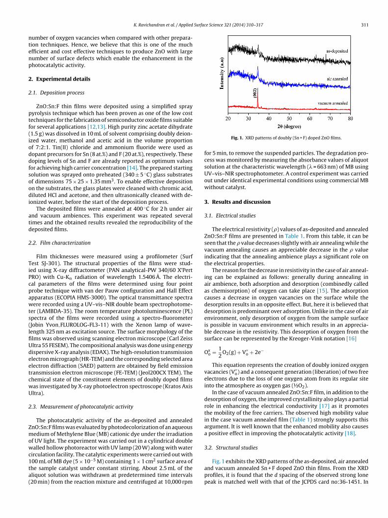
Surface Science 321 (2014) 310–317 311
ntenp
2
2
ptf(ioddfsoodi
atd
2
TiPcpawts(lfiUdeetcwU
2
Zmowc1ta(
K. Ravichandran et al. / Applied
umber of oxygen vacancies when compared with other prepara-ion techniques. Hence, we believe that this is one of the muchfficient and cost effective techniques to produce ZnO with largeumber of surface defects which enable the enhancement in thehotocatalytic activity.
. Experimental details
.1. Deposition process
ZnO:Sn:F thin films were deposited using a simplified sprayyrolysis technique which has been proven as one of the low costechniques for the fabrication of semiconductor oxide films suitableor several applications [12,13]. High purity zinc acetate dihydrate1.5 g) was dissolved in 10 mL of solvent comprising doubly deion-zed water, methanol and acetic acid in the volume proportionf 7:2:1. Tin(II) chloride and ammonium fluoride were used asopant precursors for Sn (8 at.%) and F (20 at.%), respectively. Theseoping levels of Sn and F are already reported as optimum valuesor achieving high carrier concentration [14]. The prepared startingolution was sprayed onto preheated (340 ± 5 ◦C) glass substratesf dimensions 75 × 25 × 1.35 mm3. To enable effective depositionn the substrates, the glass plates were cleaned with chromic acid,iluted HCl and acetone, and then ultrasonically cleaned with de-
onized water, before the start of the deposition process.The deposited films were annealed at 400 ◦C for 2 h under air
nd vacuum ambiences. This experiment was repeated severalimes and the obtained results revealed the reproducibility of theeposited films.
.2. Film characterization
Film thicknesses were measured using a profilometer (Surfest SJ-301). The structural properties of the films were stud-ed using X-ray diffractometer (PAN analytical-PW 340/60 X’PertRO) with Cu-K� radiation of wavelength 1.5406 A. The electri-al parameters of the films were determined using four pointrobe technique with van der Pauw configuration and Hall Effectpparatus (ECOPIA HMS-3000). The optical transmittance spectraere recorded using a UV–vis–NIR double beam spectrophotome-
er (LAMBDA-35). The room temperature photoluminescence (PL)pectra of the films were recorded using a spectro-fluorometerJobin Yvon FLUROLOG-FL3-11) with the Xenon lamp of wave-ength 325 nm as excitation source. The surface morphology of thelms was observed using scanning electron microscope (Carl Zeissltra 55 FESEM). The compositional analysis was done using energyispersive X-ray analysis (EDAX). The high-resolution transmissionlectron micrograph (HR-TEM) and the corresponding selected arealectron diffraction (SAED) pattern are obtained by field emissionransmission electron microscope (FE-TEM) (Jeol200CX TEM). Thehemical state of the constituent elements of doubly doped filmsas investigated by X-ray photoelectron spectroscope (Kratos Axisltra).
.3. Measurement of photocatalytic activity
The photocatalytic activity of the as-deposited and annealednO:Sn:F films was evaluated by photodecolorization of an aqueousedium of Methylene Blue (MB) cationic dye under the irradiation
f UV light. The experiment was carried out in a cylindrical doublealled hollow photoreactor with UV lamp (20 W) along with water
irculation facility. The catalytic experiments were carried out with
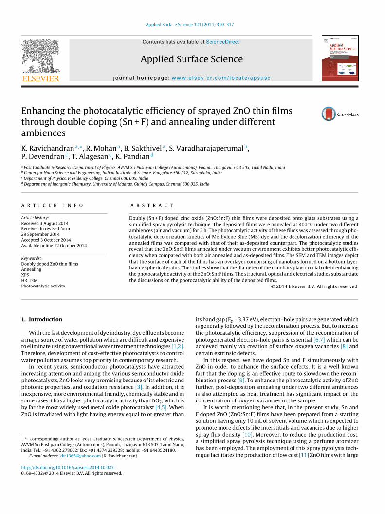
00 mL of MB dye (5 × 10⁻⁵ M) containing 1 × 1 cm2 surface area ofhe sample catalyst under constant stirring. About 2.5 mL of theliquot solution was withdrawn at predetermined time intervals20 min) from the reaction mixture and centrifuged at 10,000 rpmFig. 1. XRD patterns of doubly (Sn + F) doped ZnO films.
for 5 min, to remove the suspended particles. The degradation pro-cess was monitored by measuring the absorbance values of aliquotsolution at the characteristic wavelength (� = 663 nm) of MB usingUV–vis–NIR spectrophotometer. A control experiment was carriedout under identical experimental conditions using commercial MBwithout catalyst.
3. Results and discussion
3.1. Electrical studies
The electrical resistivity (�) values of as-deposited and annealedZnO:Sn:F films are presented in Table 1. From this table, it can beseen that the � value decreases slightly with air annealing while thevacuum annealing causes an appreciable decrease in the � valueindicating that the annealing ambience plays a significant role onthe electrical properties.
The reason for the decrease in resistivity in the case of air anneal-ing can be explained as follows: generally during annealing inair ambience, both adsorption and desorption (combinedly calledas chemisorption) of oxygen can take place [15]. The adsorptioncauses a decrease in oxygen vacancies on the surface while thedesorption results in an opposite effect. But, here it is believed thatdesorption is predominant over adsorption. Unlike in the case of airenvironment, only desorption of oxygen from the sample surfaceis possible in vacuum environment which results in an apprecia-ble decrease in the resistivity. This desorption of oxygen from thesurface can be represented by the Kreoger-Vink notation [16]
Oxo = 1
2O2(g) + V′′
o + 2e−
This equation represents the creation of doubly ionized oxygenvacancies (V′′
o) and a consequent generation (liberation) of two freeelectrons due to the loss of one oxygen atom from its regular siteinto the atmosphere as oxygen gas (½O2).
In the case of vacuum annealed ZnO:Sn:F film, in addition to thedesorption of oxygen, the improved crystallinity also plays a partialrole in enhancing the electrical conductivity [17] as it promotesthe mobility of the free carriers. The observed high mobility valuein the case vacuum annealed film (Table 1) strongly supports thisargument. It is well known that the enhanced mobility also causesa positive effect in improving the photocatalytic activity [18].
3.2. Structural studies
Fig. 1 exhibits the XRD patterns of the as-deposited, air annealedand vacuum annealed Sn + F doped ZnO thin films. From the XRDprofiles, it is found that the d spacing of the observed strong lonepeak is matched well with that of the JCPDS card no:36-1451. In
312 K. Ravichandran et al. / Applied Surface Science 321 (2014) 310–317
Table 1Electrical, optical and photocatalytic reaction parameters of ZnO:Sn:F films.
Sample Resistivity (�),� cm × 10−3
Carrier concentration(n)/cm3 × 1020
Mobility (�),cm2 V−1 s−1
Optical band gap (Eg),eV
Rate constant (k),min−1
R2
1
0
4
tstniiiresaacam
otiMattpdtvapnoa
3
aa
As-deposited 1.34 0.826 56.5Air annealed 1.06 0.942 62.6Vacuum annealed 0.69 1.345 67.3
he case of as-deposited film, a single X-ray diffraction line corre-ponding to (0 0 2) plane is observed along with a broad hump onhe lower angle side of the pattern which indicates the amorphousature of the film. The air annealing does not make any significant
mprovement in the crystalline quality of the films. Only a slightncrease in the intensity of (0 0 2) diffraction line and a reductionn the FWHM are observed after air annealing as reported by otheresearchers [19,20]. But, the vacuum annealing causes a phenom-nal enhancement in the crystalline quality as evidenced by theubstantial increase in the intensity of the (0 0 2) diffraction linend the almost complete vanishing of the hump. Even though thennealing treatment is given at the same temperature in both theases, this drastic difference in the obtained results implies that thennealing atmosphere plays a decisive role in the re-crystallizationechanism.In the case of vacuum annealing, theoretically there is no loss
f thermal energy due to convection. Therefore, more amount ofhermal energy is available for the re-crystallization process dur-ng vacuum annealing, resulting in a better crystalline quality [21].
oreover, the better crystalline quality acquired by the vacuumnnealed films than the air annealed films can be explained onhe basis of sharing of the thermal energy provided by annealingreatment, by various activities involved in the re-crystallizationrocess. For instance, in the case of air annealing, generally, bothesorption and adsorption of oxygen are possible which utilize cer-ain proportion of the total energy supplied. But, in the case ofacuum annealing, only desorption can take place and therefore,
larger proportion of energy is available for the removal of amor-hous components of the material, resulting in a better crystallineature. The absence of amorphous components in the XRD patternf vacuum annealed film (Fig. 1) stands as a clear evidence of thisrgument.
.3. Optical studies
Fig. 2 shows the transmittance spectra of as-deposited andnnealed ZnO:Sn:F films. From this figure, it is obvious that theverage optical transmittance of as-deposited ZnO:Sn:F film is 75%
Fig. 2. Transmittance spectra of ZnO:Sn:F films (inset – dT/d� vs. �avg plots).
3.13 0.0032 0.93363.16 0.0079 0.99303.18 0.0086 0.9940
and it improves after post-deposition heat treatment, irrespectiveof the annealing ambience. This enhancement in transmittance ismore pronounced in vacuum than in air ambience.
The annealing of ZnO:Sn:F film in air ambience results in a slightblue shift of absorption edge whereas the vacuum ambience leadsto a further shift indicating an increase in the band gap. Theseresults are reflected in the changes in free carrier concentrationas discussed in electrical studies (Section 3.1). The observed vari-ation in the concentration of free carriers and the correspondingvariation in the optical band gap can be correlated with each other,according to the Moss–Burstein (MB) effect [22].
The optical band gap (Eg) values were calculated using the plotsdrawn between the first derivative of transmittance with respectto wavelength and average wavelength (dT/d� vs. �avg) (inset ofFig. 2) [23]. The Eg value of vacuum annealed ZnO:Sn:F film wasaround 3.18 eV which is larger than those corresponding to the as-deposited and air annealed samples (Table 1).
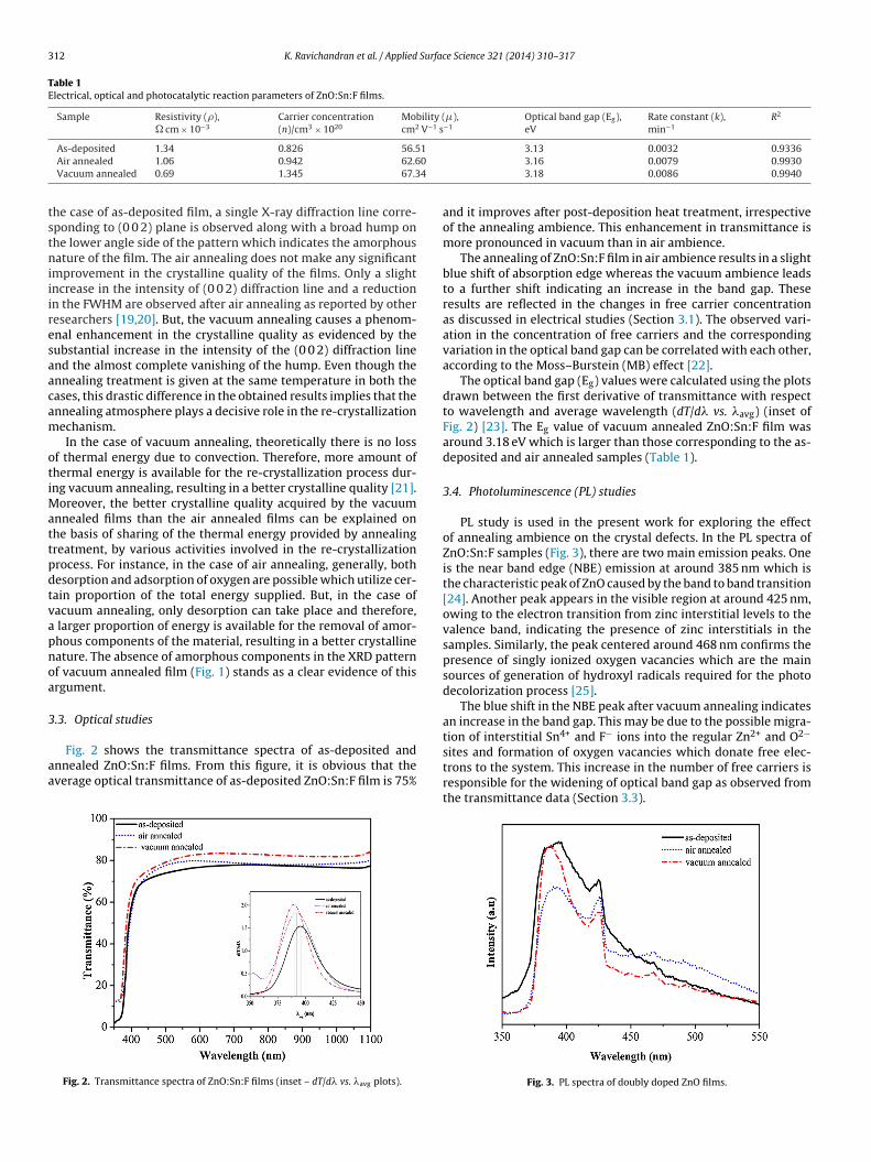
3.4. Photoluminescence (PL) studies
PL study is used in the present work for exploring the effectof annealing ambience on the crystal defects. In the PL spectra ofZnO:Sn:F samples (Fig. 3), there are two main emission peaks. Oneis the near band edge (NBE) emission at around 385 nm which isthe characteristic peak of ZnO caused by the band to band transition[24]. Another peak appears in the visible region at around 425 nm,owing to the electron transition from zinc interstitial levels to thevalence band, indicating the presence of zinc interstitials in thesamples. Similarly, the peak centered around 468 nm confirms thepresence of singly ionized oxygen vacancies which are the mainsources of generation of hydroxyl radicals required for the photodecolorization process [25].
The blue shift in the NBE peak after vacuum annealing indicatesan increase in the band gap. This may be due to the possible migra-tion of interstitial Sn4+ and F− ions into the regular Zn2+ and O2−
sites and formation of oxygen vacancies which donate free elec-trons to the system. This increase in the number of free carriers isresponsible for the widening of optical band gap as observed fromthe transmittance data (Section 3.3).
Fig. 3. PL spectra of doubly doped ZnO films.
K. Ravichandran et al. / Applied Surface Science 321 (2014) 310–317 313
hotoc
3
ZptewTat[
Fig. 4. Basic mechanism of p
.5. Photocatalytic activity of Methylene Blue (MB)
The photocatalytic activity of as-deposited and annealednO:Sn:F films on Methylene Blue (MB) dye was evaluated by thehoto decolorization of the dye under UV light. In general, the pho-ocatalytic degradation is proposed to involve the generation oflectron–hole (e−/h+) pairs when the photocatalyst is irradiatedith a photon of energy equal to or greater than its band gap.
hese e−/h+ pairs get transferred to the surface of the photocatalystnd interact with the dye molecules to participate in redox reac-ions and as a consequence, the dye molecules degrade as follows26,27]:
Fig. 5. Absorbance spectra of Methylene Blue (MB) dye solution containing (a) as-dep
atalytic activity of ZnO:Sn:F.
ZnO + h� → ZnO(e− + h+)
e− + O2 → O · −2
h+ + H2O → OH · + H+
O · −2 /OH · + dye → dyeredox → intermediates → CO2 + H2O
The basic mechanism of the photocatalytic activity of ZnO:Sn:Ffilms is presented in Fig. 4. Fig. 5a–c shows the absorbance
osited, (b) air annealed, (c) vacuum annealed ZnO:Sn:F films and (d) no catalyst.
3 Surface Science 321 (2014) 310–317
sesatucldpii
m
�
wtt
sce[dc
14 K. Ravichandran et al. / Applied
pectra of MB, recorded at different irradiation times in the pres-nce of the as-deposited, air annealed and vacuum annealedamples. For comparison, the spectra observed without a photocat-lyst is also given in Fig. 5d. When the photocatalyst is involved inhe photo de-colorization process, the absorbance decreases grad-ally with the increase in time of irradiation whereas no noticeablehange in absorbance is observed in the absence of photocata-yst. A close observation of the Fig. 6 clearly suggests that thee-colorization efficiency of the annealed films is higher when com-ared with that of as-deposited film. Moreover, this enhancement
n the photocatalytic de-colorization efficiency is more pronouncedn the case of vacuum annealed film.
The de-colorization efficiency can be calculated from the for-ula [28]
= Co − C
Co× 100 = Ao − A
Ao× 100
here C0 and C are the dye’s initial concentration and the concen-ration after the irradiation time ‘t’, respectively and A0 and A arehe corresponding absorbance values.
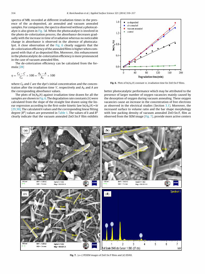
The plots of ln(A0/A) against irradiation time drawn for all theamples are shown in Fig. 6. The degradation rate constants (k) werealculated from the slope of the straight line drawn using the lin-
ar regression according to the first-order kinetic law ln(A0/A) = kt29,30]. The calculated k values and the corresponding linear fittingegree (R2) values are presented in Table 1. The values of k and R2learly indicate that the vacuum annealed ZnO:Sn:F film exhibits
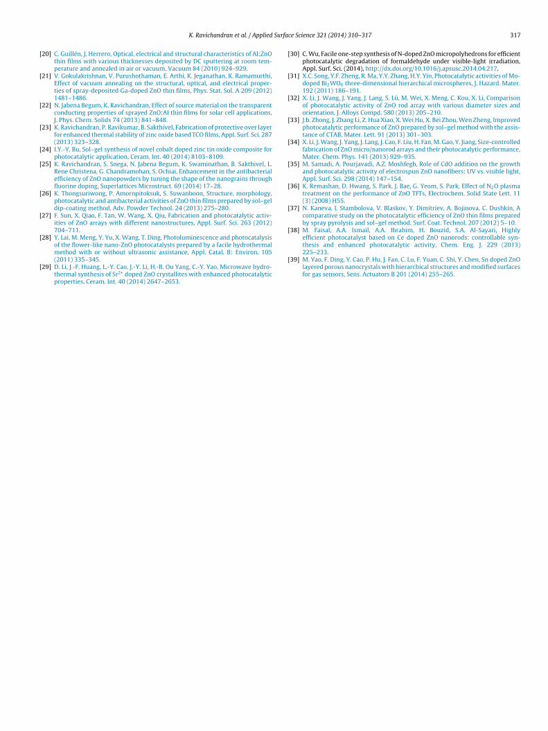
Fig. 7. (a–c) FESEM images of Zn
Fig. 6. Plots of ln(A0/A) constant vs. irradiation time for ZnO:Sn:F films.
better photocatalytic performance which may be attributed to thepresence of larger number of oxygen vacancies mainly caused bythe desorption of oxygen during vacuum annealing. These oxygenvacancies cause an increase in the concentration of free electrons
as observed in the electrical studies (Section 3.1). Moreover, theincreased surface to volume ratio and the bar shape morphologywith low packing density of vacuum annealed ZnO:Sn:F, film asobserved from the SEM image (Fig. 7), provide more active centersO:Sn:F films and (d) EDAX.
K. Ravichandran et al. / Applied Surface Science 321 (2014) 310–317 315
Fig. 8. (a) TEM and (b) HR-TEM image (inset – SAED pattern) of vacuum annealed ZnO:Sn:F film.
Fig. 9. (a) XPS survey spectrum and high resolution spectra of (b) Zn
2p, (c) Sn 3d and (d) O 1s for vacuum annealed ZnO:Sn:F film.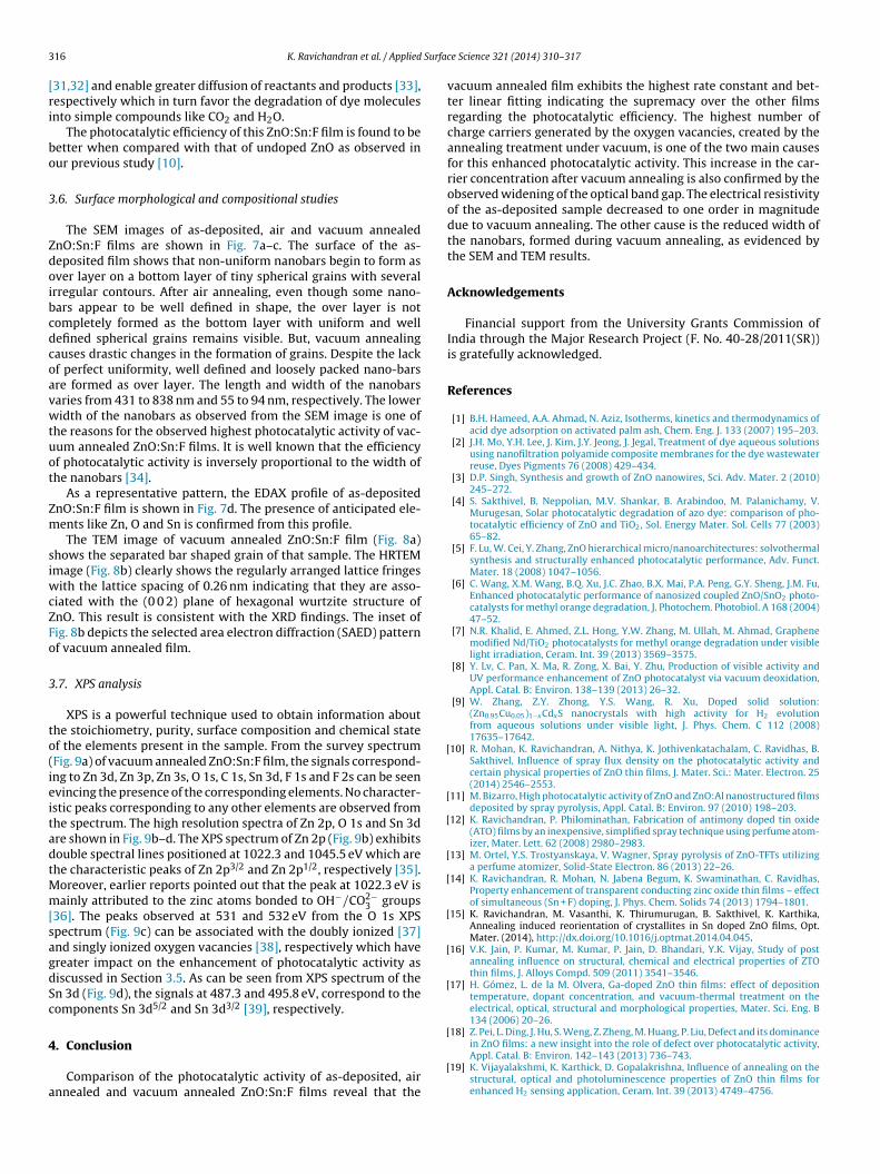
3 Surfac
[ri
bo
3
Zdoibcdcoavwtuot
Zm
siwcZFo
3
to(ieitadtMm[sagdSc
4
a
[
[
[
[
[
[
[
[
[
16 K. Ravichandran et al. / Applied
31,32] and enable greater diffusion of reactants and products [33],espectively which in turn favor the degradation of dye moleculesnto simple compounds like CO2 and H2O.
The photocatalytic efficiency of this ZnO:Sn:F film is found to beetter when compared with that of undoped ZnO as observed inur previous study [10].
.6. Surface morphological and compositional studies
The SEM images of as-deposited, air and vacuum annealednO:Sn:F films are shown in Fig. 7a–c. The surface of the as-eposited film shows that non-uniform nanobars begin to form asver layer on a bottom layer of tiny spherical grains with severalrregular contours. After air annealing, even though some nano-ars appear to be well defined in shape, the over layer is notompletely formed as the bottom layer with uniform and wellefined spherical grains remains visible. But, vacuum annealingauses drastic changes in the formation of grains. Despite the lackf perfect uniformity, well defined and loosely packed nano-barsre formed as over layer. The length and width of the nanobarsaries from 431 to 838 nm and 55 to 94 nm, respectively. The loweridth of the nanobars as observed from the SEM image is one of
he reasons for the observed highest photocatalytic activity of vac-um annealed ZnO:Sn:F films. It is well known that the efficiencyf photocatalytic activity is inversely proportional to the width ofhe nanobars [34].
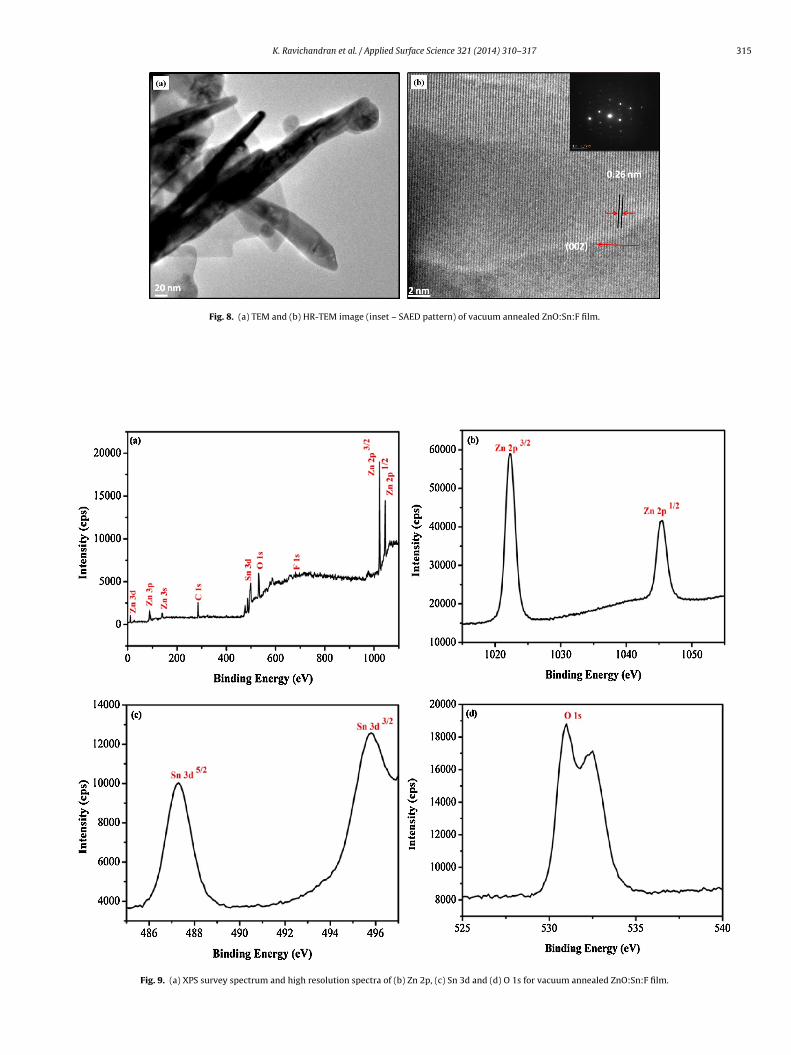
As a representative pattern, the EDAX profile of as-depositednO:Sn:F film is shown in Fig. 7d. The presence of anticipated ele-ents like Zn, O and Sn is confirmed from this profile.The TEM image of vacuum annealed ZnO:Sn:F film (Fig. 8a)
hows the separated bar shaped grain of that sample. The HRTEMmage (Fig. 8b) clearly shows the regularly arranged lattice fringes
ith the lattice spacing of 0.26 nm indicating that they are asso-iated with the (0 0 2) plane of hexagonal wurtzite structure ofnO. This result is consistent with the XRD findings. The inset ofig. 8b depicts the selected area electron diffraction (SAED) patternf vacuum annealed film.
.7. XPS analysis
XPS is a powerful technique used to obtain information abouthe stoichiometry, purity, surface composition and chemical statef the elements present in the sample. From the survey spectrumFig. 9a) of vacuum annealed ZnO:Sn:F film, the signals correspond-ng to Zn 3d, Zn 3p, Zn 3s, O 1s, C 1s, Sn 3d, F 1s and F 2s can be seenvincing the presence of the corresponding elements. No character-stic peaks corresponding to any other elements are observed fromhe spectrum. The high resolution spectra of Zn 2p, O 1s and Sn 3dre shown in Fig. 9b–d. The XPS spectrum of Zn 2p (Fig. 9b) exhibitsouble spectral lines positioned at 1022.3 and 1045.5 eV which arehe characteristic peaks of Zn 2p3/2 and Zn 2p1/2, respectively [35].
oreover, earlier reports pointed out that the peak at 1022.3 eV isainly attributed to the zinc atoms bonded to OH−/CO2−
3 groups36]. The peaks observed at 531 and 532 eV from the O 1s XPSpectrum (Fig. 9c) can be associated with the doubly ionized [37]nd singly ionized oxygen vacancies [38], respectively which havereater impact on the enhancement of photocatalytic activity asiscussed in Section 3.5. As can be seen from XPS spectrum of then 3d (Fig. 9d), the signals at 487.3 and 495.8 eV, correspond to theomponents Sn 3d5/2 and Sn 3d3/2 [39], respectively.
. Conclusion
Comparison of the photocatalytic activity of as-deposited, airnnealed and vacuum annealed ZnO:Sn:F films reveal that the
[
e Science 321 (2014) 310–317
vacuum annealed film exhibits the highest rate constant and bet-ter linear fitting indicating the supremacy over the other filmsregarding the photocatalytic efficiency. The highest number ofcharge carriers generated by the oxygen vacancies, created by theannealing treatment under vacuum, is one of the two main causesfor this enhanced photocatalytic activity. This increase in the car-rier concentration after vacuum annealing is also confirmed by theobserved widening of the optical band gap. The electrical resistivityof the as-deposited sample decreased to one order in magnitudedue to vacuum annealing. The other cause is the reduced width ofthe nanobars, formed during vacuum annealing, as evidenced bythe SEM and TEM results.
Acknowledgements
Financial support from the University Grants Commission ofIndia through the Major Research Project (F. No. 40-28/2011(SR))is gratefully acknowledged.
References
[1] B.H. Hameed, A.A. Ahmad, N. Aziz, Isotherms, kinetics and thermodynamics ofacid dye adsorption on activated palm ash, Chem. Eng. J. 133 (2007) 195–203.
[2] J.H. Mo, Y.H. Lee, J. Kim, J.Y. Jeong, J. Jegal, Treatment of dye aqueous solutionsusing nanofiltration polyamide composite membranes for the dye wastewaterreuse, Dyes Pigments 76 (2008) 429–434.
[3] D.P. Singh, Synthesis and growth of ZnO nanowires, Sci. Adv. Mater. 2 (2010)245–272.
[4] S. Sakthivel, B. Neppolian, M.V. Shankar, B. Arabindoo, M. Palanichamy, V.Murugesan, Solar photocatalytic degradation of azo dye: comparison of pho-tocatalytic efficiency of ZnO and TiO2, Sol. Energy Mater. Sol. Cells 77 (2003)65–82.
[5] F. Lu, W. Cei, Y. Zhang, ZnO hierarchical micro/nanoarchitectures: solvothermalsynthesis and structurally enhanced photocatalytic performance, Adv. Funct.Mater. 18 (2008) 1047–1056.
[6] C. Wang, X.M. Wang, B.Q. Xu, J.C. Zhao, B.X. Mai, P.A. Peng, G.Y. Sheng, J.M. Fu,Enhanced photocatalytic performance of nanosized coupled ZnO/SnO2 photo-catalysts for methyl orange degradation, J. Photochem. Photobiol. A 168 (2004)47–52.
[7] N.R. Khalid, E. Ahmed, Z.L. Hong, Y.W. Zhang, M. Ullah, M. Ahmad, Graphenemodified Nd/TiO2 photocatalysts for methyl orange degradation under visiblelight irradiation, Ceram. Int. 39 (2013) 3569–3575.
[8] Y. Lv, C. Pan, X. Ma, R. Zong, X. Bai, Y. Zhu, Production of visible activity andUV performance enhancement of ZnO photocatalyst via vacuum deoxidation,Appl. Catal. B: Environ. 138–139 (2013) 26–32.
[9] W. Zhang, Z.Y. Zhong, Y.S. Wang, R. Xu, Doped solid solution:(Zn0.95Cu0.05)1−xCdxS nanocrystals with high activity for H2 evolutionfrom aqueous solutions under visible light, J. Phys. Chem. C 112 (2008)17635–17642.
10] R. Mohan, K. Ravichandran, A. Nithya, K. Jothivenkatachalam, C. Ravidhas, B.Sakthivel, Influence of spray flux density on the photocatalytic activity andcertain physical properties of ZnO thin films, J. Mater. Sci.: Mater. Electron. 25(2014) 2546–2553.
11] M. Bizarro, High photocatalytic activity of ZnO and ZnO:Al nanostructured filmsdeposited by spray pyrolysis, Appl. Catal. B: Environ. 97 (2010) 198–203.
12] K. Ravichandran, P. Philominathan, Fabrication of antimony doped tin oxide(ATO) films by an inexpensive, simplified spray technique using perfume atom-izer, Mater. Lett. 62 (2008) 2980–2983.
13] M. Ortel, Y.S. Trostyanskaya, V. Wagner, Spray pyrolysis of ZnO-TFTs utilizinga perfume atomizer, Solid-State Electron. 86 (2013) 22–26.
14] K. Ravichandran, R. Mohan, N. Jabena Begum, K. Swaminathan, C. Ravidhas,Property enhancement of transparent conducting zinc oxide thin films – effectof simultaneous (Sn + F) doping, J. Phys. Chem. Solids 74 (2013) 1794–1801.
15] K. Ravichandran, M. Vasanthi, K. Thirumurugan, B. Sakthivel, K. Karthika,Annealing induced reorientation of crystallites in Sn doped ZnO films, Opt.Mater. (2014), http://dx.doi.org/10.1016/j.optmat.2014.04.045.
16] V.K. Jain, P. Kumar, M. Kumar, P. Jain, D. Bhandari, Y.K. Vijay, Study of postannealing influence on structural, chemical and electrical properties of ZTOthin films, J. Alloys Compd. 509 (2011) 3541–3546.
17] H. Gómez, L. de la M. Olvera, Ga-doped ZnO thin films: effect of depositiontemperature, dopant concentration, and vacuum-thermal treatment on theelectrical, optical, structural and morphological properties, Mater. Sci. Eng. B134 (2006) 20–26.
18] Z. Pei, L. Ding, J. Hu, S. Weng, Z. Zheng, M. Huang, P. Liu, Defect and its dominance
in ZnO films: a new insight into the role of defect over photocatalytic activity,Appl. Catal. B: Environ. 142–143 (2013) 736–743.19] K. Vijayalakshmi, K. Karthick, D. Gopalakrishna, Influence of annealing on thestructural, optical and photoluminescence properties of ZnO thin films forenhanced H2 sensing application, Ceram. Int. 39 (2013) 4749–4756.
Surfac
[
[
[
[
[
[
[
[
[
[
[
[
[
[
[
[
[
[
[
thesis and enhanced photocatalytic activity, Chem. Eng. J. 229 (2013)
K. Ravichandran et al. / Applied
20] C. Guillén, J. Herrero, Optical, electrical and structural characteristics of Al:ZnOthin films with various thicknesses deposited by DC sputtering at room tem-perature and annealed in air or vacuum, Vacuum 84 (2010) 924–929.
21] V. Gokulakrishnan, V. Purushothaman, E. Arthi, K. Jeganathan, K. Ramamurthi,Effect of vacuum annealing on the structural, optical, and electrical proper-ties of spray-deposited Ga-doped ZnO thin films, Phys. Stat. Sol. A 209 (2012)1481–1486.
22] N. Jabena Begum, K. Ravichandran, Effect of source material on the transparentconducting properties of sprayed ZnO:Al thin films for solar cell applications,J. Phys. Chem. Solids 74 (2013) 841–848.
23] K. Ravichandran, P. Ravikumar, B. Sakthivel, Fabrication of protective over layerfor enhanced thermal stability of zinc oxide based TCO films, Appl. Surf. Sci. 287(2013) 323–328.
24] I.Y.-Y. Bu, Sol–gel synthesis of novel cobalt doped zinc tin oxide composite forphotocatalytic application, Ceram. Int. 40 (2014) 8103–8109.
25] K. Ravichandran, S. Snega, N. Jabena Begum, K. Swaminathan, B. Sakthivel, L.Rene Christena, G. Chandramohan, S. Ochiai, Enhancement in the antibacterialefficiency of ZnO nanopowders by tuning the shape of the nanograins throughfluorine doping, Superlattices Microstruct. 69 (2014) 17–28.
26] K. Thongsuriwong, P. Amornpitoksuk, S. Suwanboon, Structure, morphology,photocatalytic and antibacterial activities of ZnO thin films prepared by sol–geldip-coating method, Adv. Powder Technol. 24 (2013) 275–280.
27] F. Sun, X. Qiao, F. Tan, W. Wang, X. Qiu, Fabrication and photocatalytic activ-ities of ZnO arrays with different nanostructures, Appl. Surf. Sci. 263 (2012)704–711.
28] Y. Lai, M. Meng, Y. Yu, X. Wang, T. Ding, Photoluminescence and photocatalysisof the flower-like nano-ZnO photocatalysts prepared by a facile hydrothermal
method with or without ultrasonic assistance, Appl. Catal. B: Environ. 105(2011) 335–345.29] D. Li, J.-F. Huang, L.-Y. Cao, J.-Y. Li, H.-B. Ou Yang, C.-Y. Yao, Microwave hydro-thermal synthesis of Sr2+ doped ZnO crystallites with enhanced photocatalyticproperties, Ceram. Int. 40 (2014) 2647–2653.
[
e Science 321 (2014) 310–317 317
30] C. Wu, Facile one-step synthesis of N-doped ZnO micropolyhedrons for efficientphotocatalytic degradation of formaldehyde under visible-light irradiation,Appl. Surf. Sci. (2014), http://dx.doi.org/10.1016/j.apsusc.2014.04.217.
31] X.C. Song, Y.F. Zheng, R. Ma, Y.Y. Zhang, H.Y. Yin, Photocatalytic activities of Mo-doped Bi2WO6 three-dimensional hierarchical microspheres, J. Hazard. Mater.192 (2011) 186–191.
32] X. Li, J. Wang, J. Yang, J. Lang, S. Lü, M. Wei, X. Meng, C. Kou, X. Li, Comparisonof photocatalytic activity of ZnO rod array with various diameter sizes andorientation, J. Alloys Compd. 580 (2013) 205–210.
33] J.b. Zhong, J. Zhang Li, Z. Hua Xiao, X. Wei Hu, X. Bei Zhou, Wen Zheng, Improvedphotocatalytic performance of ZnO prepared by sol–gel method with the assis-tance of CTAB, Mater. Lett. 91 (2013) 301–303.
34] X. Li, J. Wang, J. Yang, J. Lang, J. Cao, F. Liu, H. Fan, M. Gao, Y. Jiang, Size-controlledfabrication of ZnO micro/nanorod arrays and their photocatalytic performance,Mater. Chem. Phys. 141 (2013) 929–935.
35] M. Samadi, A. Pourjavadi, A.Z. Moshfegh, Role of CdO addition on the growthand photocatalytic activity of electrospun ZnO nanofibers: UV vs. visible light,Appl. Surf. Sci. 298 (2014) 147–154.
36] K. Remashan, D. Hwang, S. Park, J. Bae, G. Yeom, S. Park, Effect of N2O plasmatreatment on the performance of ZnO TFTs, Electrochem. Solid State Lett. 11(3) (2008) H55.
37] N. Kaneva, I. Stambolova, V. Blaskov, Y. Dimitriev, A. Bojinova, C. Dushkin, Acomparative study on the photocatalytic efficiency of ZnO thin films preparedby spray pyrolysis and sol–gel method, Surf. Coat. Technol. 207 (2012) 5–10.
38] M. Faisal, A.A. Ismail, A.A. Ibrahim, H. Bouzid, S.A. Al-Sayari, Highlyefficient photocatalyst based on Ce doped ZnO nanorods: controllable syn-
225–233.39] M. Yao, F. Ding, Y. Cao, P. Hu, J. Fan, C. Lu, F. Yuan, C. Shi, Y. Chen, Sn doped ZnO
layered porous nanocrystals with hierarchical structures and modified surfacesfor gas sensors, Sens. Actuators B 201 (2014) 255–265.