EMP AWARENESS COURSE NOTES - DTIC
260
AD-A058 .367 r DNA 2772T ADA 058-367 SDNA EMP AWARENESS COURSE NOTES S Third Edition lIT Research Institute 10 West 35th Street Chicago, Illinois 60616 October 1977 Topical Report CONTRACT No. DNA 001-75-C-0074 f, APPROVED FOR PUBLIC R2LEASE; DISTIBUTION UNLIMITED. THIS WORK SPONSORED BY THE DEFENSE- NUCLEAR AGENCY UNDER RDT&E RMSS COUE X323075469 075QAXECO9201 H259OD. PIOCIWUCID by * NATIONAL TECHNICAL INFORMATION SERVICE 1J. DEPA~IIji!I Of ¢ Rg I Prepared for Director DEFENSE NUCLEAR AGENCY Washington, D. C. 20305 kill
-
Upload
khangminh22 -
Category
Documents
-
view
1 -
download
0
Transcript of EMP AWARENESS COURSE NOTES - DTIC

AD-A058 .367
r DNA 2772TADA 058-367
SDNA EMP AWARENESS COURSE NOTES
S Third Edition
lIT Research Institute
10 West 35th StreetChicago, Illinois 60616
October 1977
Topical Report
CONTRACT No. DNA 001-75-C-0074
f, APPROVED FOR PUBLIC R2LEASE;DISTIBUTION UNLIMITED.
THIS WORK SPONSORED BY THE DEFENSE- NUCLEAR AGENCYUNDER RDT&E RMSS COUE X323075469 075QAXECO9201 H259OD.
PIOCIWUCID by* NATIONAL TECHNICALINFORMATION SERVICE
1J. DEPA~IIji!I Of ¢ Rg I
Prepared forDirector
DEFENSE NUCLEAR AGENCY
Washington, D. C. 20305
kill
UNCLASS IFIlEDSECURITY CL.ASSIFICATION Of THIS PAGE flhsies Data Entered) __________________
i EOTDCUETTO AGE READ INSTRUCTIONS_______________ _______________________ BEFORECOMPLETINGFORMI
I.REPORT NUMBER 2. GOVT ACCESSION NO0. 3. RIECIPIENT'S CATALOG NUMBER
DNA '2772Tj4. TITLE (and Sbtl)S. TYPE OF REPORT & PERIOD COVERED
DNA EI-9 AWARENESS COURSE NOTES .Topical. ReportThird Edition, S. PERFORMING ORo. REPORT HUMDER
7. AUTH~OR($) 6. CONT-RACT OR GRANT NUMUER(2)
I. N. 'Minde]. DNA 001-75-C-0074
S. PERFORMING ORGANI1Z ATION NAME AND .ADDRESS 10. PROGRAM ELEMENT.PROJECT, TASK
TIT Research Institute' AREA & WORK UNIT NUMBERS
10 West 35th Street t4WED SubtaskChcago, I inoi 601 I_______ Q7QXC9-0
II. CONTROLLING OFFICt NAME AND ADDRESS 1Z. REPORT DATE
Director October 1977 ____
Defense Nuclear Agency 11 NUMBER OF PAGES
Washington, D.C. 20305 278______ ___
I MONITORING AGENCY NAMtS, AOOREFSS(it different froms ContiolIiJag Officei) I5. SECURITY CLASS (of this eeport)
UNCLASSIFIED15a. DECLASSIFICATION.'DOWNGRADING,
SCm EOU L r
IS. VISTR19UTION STATEMiENT (of this Report)
SApproved for public release; distribution unlimited.
17. DISTRIBUTION STATEMENT (of th, abstract entered ins Block 20, it' differenit from Report)
is. S17?-PLEMEXTARY NOTES
This work sponsored by the Defense Nuclear Agency underRDT&E RMSS Code X323075469 Q75QAUC092Ol H2590D.
It. KEY WeRnS (Continue on reverse side it nscposary aid identify Iby block nwn bet)
Electromagnetic Pulse EM? Design PracticesENP Environment EMP TestingEN? System Degradation Modes EMP System HardeningEM? Interaction and Coupling
ZC0. A'ýýTR ACT (Cont'inow oti reverse aide if ruereouaf aind idotstif4 6ý' bIlics. nuinh. I
These notes are primarily intended as a guide for theindividu.al attending the~ DNA iZMP Awareness Couzae. The textserves as an engireering 11-truduction to the EMI systems desiDrablem and provides a .3urvey of techniques suitable for soiw. -,ihis hardening problem. The text discusses all aspects of EM?,from the envi~ronment through sylitem design and testing.
DD I AN 71 1473 EOITION OF I NOV 6S MS OBSOLETE UNCLASSIFIED1.SECURITY CLASSIFICATION OF THIS PAGE (Wheni Data krntorvd)

SUMMARY
This course is designed to alert management andtechnical personnel to the need for EMP protection andto the hardening techniques which can be applied. Thebulk of the course material is aimed toward those indi-viduals who may have a direct responsibility for EMPhardening of a system.
The duration of the complete course is three days.The course also includes an Overview of interest tomanagement.
The Overview is essentially an introduction to theEMP problem area. The general problems and difficultiesare reviewed.
The technical portion of the course considers allaspects of the problem area from an engineering harden-ing viewpoint. It requires approximately 2-3/4 days ofpresentation time to discuss the salient features of theinformation and background necessary to harden systems.
II
itl

,A
PREFACE
Third Edition
To maintain the course and the course notes current, updating andrevisions are a continuous effort. Since the original publication inAngust 1971, significant advances in the state-of-the-technology haveoccurred. In that regard, complete revision of the course notes wasdeemed desirable. The technical revision was performed by Mr. IrvingN. Mindel of lIT Research Institute.
The author of the course notes would like to acknowledge the lead-ership and technical review of the course and the course notes providedby Captain W. D. Wilsou and Mr. G. Baker from the Defense Nuclear Agency.Acknowledgement of the comments received from the "EMP Conmmunity" andthe course attendees has also been very beneficial to furthering theobjectives of the course. The efforts of the editorial staff of IITRI,particularly Ms. M. Leek and Ms. C. Damberger, who compiled and editedthe final publication, is gratefully acknowledged.
lIT Res~atch InstituteChicago, IllinoisOctober 1977
"2

TABLE OF CONTENTS
Section Page
I. OVERVIEW: INTRODUCTION TO THE EMP PROBLEM ........ ... .............. 1.- 1
1.1 Introduction ................. .......................... .. 1- 21.2 EMP Generation and Characteristics ......... ............... .. 1- 2
EMP Generation ................. ........................ .. 1- 2Characteristics of the Radiated Wave 1.............. - 3
1.3 Systems Impact of EMP .i....................................... 1- 5EMP Coupling to Systems ... .................... 1- 6System Sensitivity to EMP. ......................... 1- 6Examples .. .................................................... 1- 7Summary ............................... 1- 8
1.4 EMP Protection Practice ............ ..................... ... 1- 9Design and Analysis .............. ...................... ..1- 9Protection Incorporation . . . ................ -10Protecticn Concepts. ......................................... 1-10Design Practices of Protection Concepts ..... ............ .. 1-12Cabling .................... ............................ ... 1-14Testing. . .................. ............................ .. 1-14
1.5 Program Planning ................. ........................ ... 1-151.6 State-of-the-Art ................... ........................ .. 1-191.7 Summary ...................... ............................. .-. 21
II. INTRODUCTION TO THE TECHNICAL COURSE ........ ................. .. 2- 1
2.1 Course Objectives ..................................... 2- 12.2 Basic Electromagnetic Principles. ........ ................ .. 2- 22.3 EMP Characteristics .............. ....................... .. 2- 52.4 System/Equipment Characteristics ........... ................ .. 2- 62.5 Summary .................... ............................. ... 2- 7
III. EMP GENERATION AND CHARACTERISTICS .......... .................. .. 3- 1
3.1 Introduction ................... .......................... .. 3- 13.2 Basic Atomic and Nuclear Physics ........... ................ .. 3- 23.3 EMP Generation ................. ......................... ... 3- 5
Deposition Region Fields ............. ................... .. 3- 5Near Surface Burst EMP ........... ... .................... 3.- 6Air Burst EMP ................ ......................... .. 3- 7Exoatmospheric Burst EMP ............. ................... .. 3- 8
3.4 Earth Effects on Total Fields. ......... .................. .. 3-113.5 System Generated and Internal EMP ........ ................ .. 3-12
IV. EMP INTERACTION AND COUPLING ANALYSIS ........... ................ .. 4- 1
4.1 Introduction ..... .......................... 4- 14.2 EMP Interaction with Systems ............. .................. .. 4- 1
The Plane Wave ................... ........................ .. 4- 1Fields Due to EMP .............. ....................... ... 4- 3EM Induction Principles ............ .................... .. 4- 4Antennas .................. ........................... .. 4- 6
Linear Antennas .............. ....................... .. 4- 6Loop Antennas .... ............. .................... .. b.- 6
Cables ....................... ............................ .. 4- 7Shielding and Penetration .............. ................... 4-,C
Electric Field Shielding ............. .................. .. 4-12Magnetic Field Shielding ........... ................... 4-13Seams and Apertures. ........... .................... .. 4-15
Ground Effects . . . . . . . . . . . . . . . . . . . . . . .. 4-164.3 Coupling and Interaction Analysis ........ ................ .. 4-17
Role of Analysis ............. ....................... 4-17"" System Modeling ................ ........................ ... 4-18
3

TABLE OF CONTENTS
Section !age
4.4 Antenna Coupling Analysis - Linear Systems .... ........... .. 4-19Simple Energy Collectors .......... ................... .. 4-19Fourier Transform Metbod .......... ................... .. 4-22
4.5 Antenna Coupling Analysis - Nonlinear Systems ... ......... .. 4-27Parabolic Antenna Example ............. .................. .. 4-30
4.6 Structures Modelid as Antennas ........ .............. . . 4-30Missile in Flight ................. ...................... .. 4-30Microwave Tower ............... ....................... ... 4-31P-3C Aircraft ................. ....................... .. 4-32
4.7 Cable Analysis .................. ........................ .. 4-33Cables in Proximity to Conducting Surface ................... 4-13Cables in Proximity to Non-Conducting Stirface ..... 4-35Buried Cables ................... ........................ .. 4-35Surface Transfer Impedance for Shielded Cables ........... .. 4-36EMP Response of Typical Cable ........... ................ .. 4-3E
4.8 Shielding Analysis. . .............. 4-41Scattering, Theory Svlutions . . . . ............ 4-41Low Frequency Lumped Circuit Approximation .... .......... .. 4-42Apertures ......... .......................... 4-44Special Problems .............. ....................... .. 4-45
References .................. ........................... .. 4-47
V. COMPONENT AND SYSTEM DEGRADATION ............. .................. .. 5- 1
5.1 Introduction .................. .......................... .. 5- 1Definitions ................... ......................... .. 5- 1History ................... ........................... .. 5- 2
5.2 General Damage and Upset Considerations ...... ............ .. 5- 3Trends .............. ..... ............................ .. 5- 3System Configuration ............ ..................... .. 5- 4
5.3 Component Failure ............... ....................... .. 5- 5Semiconductor Device Failure ........ ................. .. 5- 6
Surface Effects ................. ...................... .. 5- 6Dielectric Breakdown . ........... .................... 1.5- 7Internal Junction Breakdown ........... ................ '- 7Thermal Failure Model ............. ................... .. 5- 9Verification of Wunsch Thermal Model. ... ............ .. 5-1iThe Damage Constant - KX ............. .................. .. 5-12Effect of Multiple Pulses ........... ................. .. 5-14Integrated Circuit Failure ........ ................. .. 5-15Interconnection Failure Modes ....... ............... .. 5-16Synergistic Effects ............... .................... .. 5-17
Resistor Failure .............. ....................... .. 5-17Failure Modes ............... ....................... .. 5-17Resistor Construction ........... .................. .. 5-18Resistor Failure Threshold ........ ................. .. 5-19Carbon Composition Resistors ........ ................ .. 5-19Film Resistors .............. ....................... .. 5-19Diffuse'd Resistors ............ ..................... .. 5-20Short Pulse Width Failure ...................... .. 5-20Summary of Resistor Failure Thresholds .... ........... .. 5-21Resistor Failure Thresholds Based on Safe
Operating Voltage ........ ................. .. 5-21Capacitor Failure ............... ..................... .. 5-22Failure Modes ............... ....................... .. 5-22Failure Thresholds ............ ..................... .. 5-23
Inductive Elements .............. ...................... .. 5-24Squibs and Detonators ............... .................... .. 5-24Terminal Protective Devices ........... ................. .. 5-24Miscellaneous Devices ............... .................... .. 5-25
4
AL .... . ... .

TABLE or CONTENTS
Section Pjj.
5.4 Cable and Connector Failure .. i............... 5-255.5 Operational Upset Mechanisms ................. 5-26
Digital Circuit Upset ........... ..................... .. 5-26Memory Erasure ............... ....................... .. 5-27Effects of Operntional Upset ............................ .. 5-28
References ................... .......................... .. 5-29
VI. DESIGN PRACTICES FOR EMP MITIGATION ..... ................ 6- 1
6.1 Introduction .................. ......................... .. 6- 16.2 Procection Philosophy ........ .. ................... 6- 1
Protection Concepts ............ ..................... .. 6- 1System Implications ............ ..................... .. 6- 2Intercommunity Relationships ........ ................ .. 6- 4
6.3 Hardening Design Practices ......... ... .................. .. 6- 4System Aspects ............. ......................... . 6- 4
System Geometry and Configuration ..... ............. .. 6- 5Zoning ................... .......................... .. 6- 5Clustering ..................... ........................ 6- 5Layering ................. ......................... ... 6- 6Ringing& ......... ................................... 6- 6Violations and Fixes ..... ....... ................... .. 6- 7
Communications and Data Transmission ..... ............ .. 6- 7Shielding .................. .......................... ... 6- 8
Wall Thickness and Material ........ ................. 6- 9Diffusion Shielding ............ .................... .. 6- 9Apertures ....................... ................. .. 6-10Gaske.s and Bonds ............ ..................... .. 6-11Open Apertures ................. ...................... .. 6-13Penetrations ............... ....................... .. 6-15
Grounding.. ................ .......................... ... 6-17Earth/Exterior Grounds .......... .................. .. 6-18Interior/Reference Grounds ........ ................ .. 6-20
Circuit Considerations -- Circuit Coupling .... .......... .. 6-21Circuit Configuration ........... ................... .. 6-22Component Distribution ........... ................... 3-22Cabling Design - Cable Types ......... ............... ...- 23
Termination of the Outer Conductor .... ........... .. 6-25Internal Conductors .......... ................... ...- 26
Protective Devices and Techniques ..... ............. .. 6-27Spectral Limiting Devices ......... ................ .. 6-27
Capacitors ................. ....................... 6-27Inductive Devices ........... ................... .. 6-28Filters ................ ........................ .. 6-29
Amplitude Limiting Devices ........ ............... .. 6-30Spark Gaps and Gas Diodes ...... ............... .. 6-30Zener and Silicon Diodes ........ ............... .. 6-31Varistors ......................................... .. 6-32
Hybrids ................ ......................... .. 6-33Electromechanical and Thermal Deiccs, . . ...... 6-33Crowbar Circuits ....... ..... ... .................... 6-33Device Construction and Installation ..... .......... .. 6-34Circumvention Techniques ........................... .. 6-35
System Constraints ....... ........................... .. 6-35Non-Threat Specific Schemes ......... ................ .. 6-35Threat Specific Schemes ........... .................. .. 6-36Coding Techniques ............ ..................... .. 6-36
Software Approache ........... ................. 6-36References ................... .......................... .. 6-37
5

TABLE OF CONTENTS
Section Page,
VII. EMP SIMULATION, INSTRUMENTATION AND TESTING ..... ............ .. 7- 1
7.1 Introduction ............. ......................... 7- 17.2 Hardness Testing Approaches .............. .................. 7- 2
Simulation Requirements. . ........ ................... .. 7- 2Test Concepts ................. ........................ ... 7- 3
Actual EMP Environment ............. .................. 7.- 3Threat Criteria Simulation ........... ................ .. 7- 3Sub-Criteria Level Coupling Tisting ..... ............ .. 7- 4Low Level Coupling Testing ................. 7- 6CW Testing ................. ........................ ... 7- 7Laboratory Testing ............. .................... .. 7- 8Scale Modeling .............. ...................... .. 7- 8Direct Injection Testing ....... ................. 7- 9Component Damage Testing ........... ................. .. 7- 9Shielding Teste .............. ...................... .. 7-10Analysis .............. .. ........................ 7-10
7.3 Transient Energy Sources ............. ................... .. 7-10Energy Sources for Component and Circuit Testing ... ...... 1-10High Level Energy Sources - Basic Energy Sourres ......... .. 7-11
Marx Generator ................. ...................... .. 7-12IL Inversion Generator ............. .................. .. 7-13Van de Graaff Generator .............. .................. 7-14Peaking and Transfer Capacitors ...... .............. .. 7-14Switches ............................................ ... 7-15CW Energy Sources ............ ..................... .. 7-15
7.4 Electromagnetic Pulse Field Simulation ..... ............ .. 7-15Bounded Wave Simulator ............. ................... .. 7-16Pulsed Radiated Wave Simulator ....... ............... .. 7-22
Biconic Atenna .............. ...................... .. 7-23Resistive Loaded Hcrizontal Dipole Antenna ............ .. 7-24Ground Effects - horizontal Polarization ... ......... .. 7-27Vertical Monocone. ............. ..................... .. 7-28Ground Effects - Vertical Polarization ..... .......... .. 7-29
CW Radiators ................... ........................ .. 7-307.5 Direct Injection Techniques .......... .................. .. 7-31
Cable Dr'vers ................ ....................... .. 7-31Shieldcd Cable Driving Techniques ..... ............... 7-32UnshieiLded Cable Driving Techniq,%es ..... ............ .. 7-35
Direct Injection on Signal Carrying Conductors . ... . 7-36Laboratory Component Tests - Cable Transfer Impedance. . . 7-38
Passive Components ............. .................... .. 7-39Terminal Protection Devices ........ ................. 7-,40Shielding Measurements ....... ... ............... 1.7-41Semiconductor Device Damage Threshold Testing ......... .. 7-43
7.6 Dimensional Scale Modeling Techniques. ............ 7-447.7 Simulation Facilities ............ ..................... .. 7-46
Bounded Wave Simulators .......... ................... .. 7-46ARES ................... ........................... .. 7-46TRESTLE .................. .......................... ... 7-46ALECS . ............................................... 7-46HEMP ................... ........................... .. 7-47TEFS ................... ........................... ... 7-47SIEGE ................................... 7-48
Long Wire Dipole Simulators ........ ................. .. 7-48Sandia Long-Wire . . . . . . . . . . . . . . . . . . . . . 7-48Martin-Marietta Lorg-Wire ................. 7-48
"6

TABLE OF CONTENTS
Section Eno
Pulsed Radiating Simulator FacilUtic4 ............ 7-49TEM4PS . . . 7-49AhSOP . . . . . . . . . . . . . . . . . . . . . . . . . . 7-49EMPRESS . . . . . . . . . . . . . . . . . . . . . . . . . . 7-49TITRI Crystal Lake Facilitv . .. .. .. . . .. . . . . . 7-49RE F . . . . . . . . . . . . . . . . . . . . . . . . . . .. 7-50
CW Radiating Facilities . . . . . . . . . . . . . . . . . . . 7-50WSMR Facilities ............. ...................... .. 7-50HDL ................... ............................ 7-50
Characteristics of Avai1abl• Simul&tor.s ............... .. 7-507.8 Test Instrumentation and Set-Up ......... ................ ... 7-52
Signal Sensing, .................. ........................ 7..52Electric Fi.eld Sensors. ................... 7-53Msgnetic Field Sensors ....... .................. .. 7-55Sensor Applications ......... .................... 7-58Voltage Probes. ............. ....................... .. 7-60Current Probes .................. ...................... 1-61Probe Applicarions ............ ..................... .. 7-61
Signal Distribution Systems ..... ................ 7-62Ha-dwire Datz Links ........... .................... .. 7-62Nonconducting Data Links ......... .................. 7-63
RF Telemetry ......... .......................... 7-63Dielectric Waveguide Transmission ..... ............ .. 7-64O)ptic.,l Transtrission .......... ................... .. 7-64
Signal Conditioning ........ ..................... 7-64Amplifiers ................................. 7-64Attenuators . ...................... 7-66Signal Dividers ............. ...................... .. 7-66Di ferentiators ard Integrators ....... ............. ... 7-67
Signal Display and Recording. ................ 7-67Oscillosýope/Cariera Recording ......... ............... .. 7-68Analog/Digital Recording. . ............... 7-70CW Recording . . . . . . . . . . . . . . . . . . . . . . . . 1-1I
Data Processing . .................... 7-71Calibration . . . . . . . . . ............ 7-72
Measurement System Calibraticn ...... ............... .. 7-73Data Recording System Calibration ..... ............. .. 7-73Data Processing System Calibration ..... ............. .. 7-74
Test Instrumentation Set-Up ........... ................. .. 7-75Test Point Acressability ...... .. ................ 7-7t.Precautions .... ............................. 7-77
Quality Assurance Testing ............. .................. 7-797.9 Test Planning ... ......................... 7-79
Pre-Test Planning ............ ..................... 7-80General Program Plan ........... . .. .......... 7-80General Test Plan ............... ...................... .. 7-81Detailcd Tesr Plan .............. ....................... 7-.82Detailed Test Plan Outline. ....... .................. 7-8.4
References. ......................... 7-85
VIII. APPROACIIES TO VULNERABILITY ASSESSMENT AND SYSTEM HARDENING.. .... 8- 1
8.1 introduction ................ ...................... 8-. I8.2 General Approach to EMP Hardening .... .............. 8- 18.3 Threat/Environment Criteria Definition ............ 8- 3
Threat Scenario ............... ....................... 8- 3System Mission. . ..................... 8- 3Nuclear Hardening Requirements ......... ................ .. 8- 3
j 8.4 Susceptibility/Vulnerabiliry Assessment ...................... 8- 4System Description ....... ...................... . 8- 4Electrical Overstress Assessment ..... .............. 8- 4
"Worst Case Analysis .................................. 8- 5Detailed Vulnerbihlity Analysis ........ .............. 8- 5
AL - - • - ,.

SECTION I
OVERVIEW:
INTRODUCTION TO THE EMP PROBLEM
1.1 INTRODUCTION
Everyone ýj aware of three majoreffects of a nuclear weapon; these areblast, thermal, and shock. There areother effects Associated with a nucleardetonation, which are equally important.Onr of these effects is the electro-magnetic pulse (EMP) which is the subjectof this awareness course.
P'annrrs iow consider EMP as apossible threac to many sophisticatedmilitary systems. Pow this has comeabout and, especially, how to achieve therequired p-otectinn will be the subjectof this introductory portion ard the moredetailed technical presentations whichfollow. These technical presentationsemphasize the engineering aspects.
Under the proper ctrcumstances a These unique properties are itssignificant portion of the energy re- extreme area of coverage, EMP beingleased during a nuclear detonation ap- capable of disrupting electrical andpears a& an ElectroMagnetic Pulae (EMP), electronic systems as far as 3,000 milesThe spectral conter.t of this-pulse con- from the site of the detonation; and thetains the frequencies or wavelengths fact that EMP can cause severe disruptionof many of our conmuercial radio and and sometimes damage when other promptmilitary electronic systems. weapon effects, such as nuclear r&di-
ation effects on electronics, blast,Another nuclear weapon effect some- thermal effects, dust debris and bio-
times confused with EMP is "blackout". logical effects are all absent. ThisAs we will see later, EMP directly af- means that a high-yield nuclear weapon,fects electrical and electronic systems. bursc above the atmosphere, could be"3lackout" on the other hand, is due to used to knock out improperly desinedan effect associated with the propa- electrical and electronic systems over agation media (the atmosphere) and dis- large area of the earth's surface with-rupts the signal path. "Blackout" has out doing any other significant damage.no direct effect on system hardware. The range of coverage of EMP is dimin-Also, EMP is a short-term transient ished if the weapon is detonated with-(microseconds) that can result in long- in the atmosphere.term disruptive effects in equipments/systems. An idea of the magnitude of the EMP
threat can be realized by comparing itsEM? effects depend on several factors electric field amplitude with the elec-
amnng which are the weapon, the burst tric fields produced by man-made sources.location, and the point of observation A typical high-level EMP pulse could havewith respect to the burst location. In an intensity of 500,000 volts per meter,this course we will be concerned with ihe This is 250 times more intense than asurface, near surface and the exoatmos- radar oeam of sufficient power to causepheric (or high altitude) burst. Empha- biological damage such as blindness orsis will be placed on the exoatmospheric sterilization. It is five million timesburst because it has two unique proper- as intense as fields created by sourcesties which are of crucial significance, in a typical metropolitan area.
1-1

Early 1960's
Interest...Peripheral
Early 1970's
Central Issue: Protection
EMP has been recognized as a po- To nnderitand how to protect ourtential threat to our electronic and systems requires some understanding ofelectrical systems since the 1960's. the EMP generation mechanisms and charac-Recently two factors have greatly in- teristics, the susceptibility charac-creased the significance of this threat: ttristics of electrizal and electronic
systems, and the various means to counterthe EMP effects.
(1) Increased sophistication innuclear strategy and weapons.
(2) Increased susceptibility of 1.2 EMP GENERATION AND CHARACTERISTICSelectronic systems due to thebroad introduction of semi- Two basic weapon detonation lo-conductors and newer electronic cations are of interest; the near surfacetechnologies and the ever- burst and the exoatmospheric burst.greater dependence on complex 4hile the basic mechanism is the same,operational hardware, the atmospheric density results in signi-
ficantly different interaction and sourceThe situation has changed so mach region characteristics.
that the central issue today isPROTECTION -- EMP Generation
* how to protect yovr system The basic mechanism for EMP gener-against the potentially-massive ation is electron scattering due to thedisruptive logic upset type collision of che prompt gamnsp with theeffects of EMP -- such as lock- molecules of the modin exposed to theing out the launch control or gamma flux. When che collision ismissile guidance subsystems with air molecules of the atmosphere re-during a critical period, sulting in a radiated wave, we have theetc; -- classic EMP. Collisions of the gamma
flux or x-rays with a system enclosure* how to protect your system (such as a satellite system), results
against the sometimes capoi- in b.' EMP which is termed close-in orcious-type EMP permanent source region EMP. In this course wedamage -- such as destroyinR will constrain ourselves to the radiatedthe front ends of HF communi- EMP fcom a high altitude or surfacecations receivers, burst.
1-2

The collision between the Semma fluxand the air molecules results in electronsbeing scattered in approximattly the samedireation as the gammas, The result im acharge separation, positively r&ha.gedcenter due to the parent molecules and anegatively charged electron cloud. Thissepazation of charges, occurring on owholesale basis, create* intense sourceregion electric and magnetic fields.This build-up of fields is ultimateal
limited by secondary conduction electronswhich flow back to the positively chargedregion ind tend to neutralize it. Thesesource igion fields are non-radiatingfields.
On the othier han~d, if the veaptcn is"�Cm��m detonatud outside the atmosphere, u~ual-
_y termed high-altitude burst, the gamnarays can travel many miles without en-countering an air molecule. Thus, if a
*hap large-yield weapon is detonated justabove the ionosphere, the source regioncar, be about 1,600 km in diameter and"about 20 km thick. The extent of theelectromagnetic fields radiated onto theearth's surface is greatly augmented bythe very large size of this source region.
To produce a radiated electromag-netic field the proper conditions ofasymmetry or inLeracLion with the earth's&eomagnetic field must exist. These con-ditions exist for both the high altitudeand surface burst, but the dominant phe-nomena is different for different burst .locations.
When a weapon is detonatud withinthe atmosphere, the gammas can travelonly relatively short distances betweencollisions and total absorption. Thisconfines the gamas (and therefore thesource region) to a volume perhaps 6 kilo-meters or so in diameter. Increase inweapon yield has relatively little effectupon the size of this intense field (or"source region"), and thus the EMP ef-fe-ts of an intra-atmospheric burst must Characteristics of the Radiated-Wavebe considered ,lithin the context of otherclose-by prompt nuclear wwapons effects. The spectrum and waveform of EMP
differ from those of any other natural orcommonly-used man-made sources. Thespectrum is broad and extends from ex-tremely low frequencies to the low end ofthe U}HF band. The time waveform indicatesa higher amplitude and much faster risetime than, for example, the fields eener-ated by a nearby lightning stroke, es-peciaily in the case of h.gh altitudeburzt.
1-3

A comparison of the waveform andspectruw of the high altitude burst andthe induction fields of a lightning strokeare shown in the figure.
SPECTRUM EMP C
COMPARISON C radnar
Frequency
WMEMP These fields are not uniform in
WAVEFORM amplitude or waveform over the enitireCOMPARISON lightning area but depend on burst location aiid
the earth's geomagnetic field, as we willTime see in Section III of che course. It
should also be recognized that no otherweapons effects accompany the EMP from ahigh-altutude burst.
Due to the fast rise times of theEMP, the spectral energy is distributed
Although a lightning stroke can have throughout the spectrum through the lowera fast rise time, low energy precurGor microwave band. Most man-made sourcesbefore the main stroke, the main stroke occupy only a narrow part of the spec-is a high amplitude (100 kV/m or greater), trum.I to 5 microsecond rise tim, and hundredsof microseconds fall time. An enormous In the case of the near surfaceamount of energy is contained in the main (0-2 km) burst within the depositionstroke. The induction field, however, ksource) region, non-rau.iating fields onwhich is of concern to systems nearby a the order of 100 kV/m electric fields (orlightning discharge is on the order of higher) with rise times of tens of nano-1 kV/m electric field. This induction seconds (approximately 50 ns) are real-field is non-radiating and therefore a ized. Outside the deposition region, alocalized field. radiating EM wave is realized. The
fields of this radiating wave at aIn the high altitude burst case, the distance of 10 km from the burst location
fields radiated onto the earth's surface are quite comparable to the close-byare of the order of 50 kV/m electric field fields of the lightning stroke. That is,with rise times of the order of 10 nano- rise times of approximately 1 to 5 micro-seconds. The wave is a radiating EM wave seconds and peak amplitude of 1 kV/mwhich results in an extremely large dis- electric field, These fields fall off astribution on the earth's surface in con- 1/R (R being the distance from the bursttrast to the localized nature of lightning, point) with distance from the burst.For a burst over the continental U.S., These fields are essentially verticalthe fields on the surface are predominant- polarized electric fields.ly horizontally polarized E fields. Sincethe burst location is outside the iono- In other words, EMP is sufficientlysphere, the coverage on the earth's sur- different frem any other electromagneticface is limited by the line-of-sight environment usually encountered thattangent radius to the earth'o surface. protection practices and components forThe figure shows the approxima e cover- non-EMP environments -- radio-frequencyage on the earth for a 100 1- (small interference, lightning, radar, etc., arecircle) and 300 km (large circle) height not directly applicable for EMPof burst over the central U.S. problems.
I -i:

1.3 SYSTEMS IMPACT OF EMP
During the era of U.S. atmcopherictesting, the existence of EMP was known,but the impact on electrical systems was -.not fully appreciated until some evidence ". ..of actual damage to components or system os s..utt.i.. An*sW.upset were accumulated. This absence ofearly evidence was due to relatively un-sophisticated test exposure hardware (suchas buildings, tanks, and jeeps) togetherwith the subtle nature of the effects.
The most sophisticated test hardware r. ..was usually associated with diagnostic ......instrumentation and this did exhibit ...... :...noticeable effects.
Numerous examples of EMP-induceddamage or disruptions were observed duringour atmospheric test programs. Thisphotograph of a damaged cable shows anarc-type puncture. Other types of de-gradation attributed to EMP ranged fromthe tripping of a street light system to Effort was also devoted toward simu-disruption of timing circuits for a com- lating experimentally the EMP field atmunications system. threat levels. Even over relatively
small areas, such as that occupied by amissile, this non-nuclear EMP simulationhas proved to be a very difficult andcostly problem because of the large ampli-tude and unique waveforms required.Shown, together with a missile beingtested within the wooden structure, is anearly (1968-1970) criteria level EMPsimulator. Later generation EMP simu-lators and illuminating structures arediscussed in Section VII.
Since the signing of the atmospherictest ban treaty, the United States effort _has refined the understanding of how EMPis generated to a point where good agree-ment exists between the theoretical re-sults and observed measurements takenduring the atmospheric tests. How EMP iscoupled into systems and how componentsand subsystems are degraded has also re-ceived emphasis. Modern sophisticated transistorized
systems have been experimentally exposedto simulated EMP environments. Thesetests show evidence of significant damageand extensive performance interference.
1-5

A Conclusion -- W 1. a Problem
The results developed from labora-tory EMP sencitivity tests on componentsand electromagnetic coupling analysisfurther confirm this experimental data. 4, 7 7
EMP Coupling to Systems .M " wn a,-
For energy to enter a system and re-sult in performance degradation, theenergy must first be collucted by thesystem. This energy collection process Mcan be considered to be the same as forany antenna system.
The asymmetrical flow of chargescaused by a nuclear explosion causeselectromagnetic fields to be radiatedaway from the burst point. These fieldscause a corresponding flow of charges, orelectrical currents, in distant metallic Herein lies an important differenceconductors. This is comparable to the between other nuclear weapons effectsway the electromagnetic fields from a TV (such as thermal, blast, and transienttransmitter set up currents in your roof- radiation) and EMP. These non-EMP effectstop TV antenna, result from just the energy incident on
the sensitive component, r.ircui.t or sub-system. In the case of EMP, the energyis gathered by antennas, long exposedcables and transmission lines, or otherlong exposed conductors. A large fractionof this gathered energy can be impressedon a sensitive component, such as atransistor, and cause either permanentdegradation (burnout) or false responses
CUR (upset) of a system.Other Effects EMP
Any metallic object exposed toelectromagnetic fields can be a collectorof electromagnetic energy; that is, actlike an antenna, even though it was neverintended to be that. Generally, the Just Energy Incident Pseudo "Focussing Effect"larger the metallic structure, the greatei on Compnent o of Energy Ctlectoris the amount of intercepted EMP energy.
System Sensitivity to EMP
The sensitivity of a system to dis-ruption due to EMP is a function of thesystem characteristics (i.e., digital oranalog, frequency of operation, configu-ration, etc.), and of the components usedin the system.
1-6

Laborator, tests have demcnstrated Most of cur electronic systems arethat vacuum tube systems are many times designed to be frequency selective, (i.e.,more resistant to permanent damage from operLte over a narrow frequency band),EMP than semiconductor systems, and 60 Hz and, therefore, respond differently tomotors even more resistant than vacuum the EMP spectrum. As we have seen, thetubes; but even motors can be damaged if EMP spectrum is very broad, but it cer-connected to a very large energy-collect- tainly is finite. Where the energying structure. couples to the system (power line,
antenna. etc.) determines the spectralThe replacement of "harder" vacuum content and the energy transmitted to
tube systems by "softer" transistors or .ensitive components within the system.integrated circuit systems was an aspect Therefore, all systems will not be sus-which wac never considered during the ceptible to EMP nor will they respond inatmospheric test period. This evolution the same manner or to the same extent.of systems using components that requireinherently less power has resulted in anincreased susceptibility to EM?. Examples
What does this mean in more specificterms? A few hypothetical system ex-amples may be illustrative. Consider acommunications complex. The most likelyEMP effect would be temporary interrup-Smorse sitoY tion cf communication service. This canoccur even though no permanent damagerequiring parts replacement occurs. WhereEMP protection was not considered, it has
asI been shown that one EMP pulse could im-, .. pair service of certain portions of the
system for as long as 20 to 40 minutes.Burnout of key components is somewhat
v.cu... • less likely, but always a possibility.
ýf .... NT •In the case of strategic systemsand some tactical systems, no Impairmentof the system can usually be tolerated,even for a few seconds. For example, EMP
Digital computers are extremely pickup in the control system of an in-sensitive to EMP. Here it makes little flight missile could perturb the flightdifference whether vacuuni tubes or tran- so much as to cause breakup of the missile,sistors are used. It can affect opera- could disrupt the count-down of missilestion of a computer by introducing false being reedied for firing, or could impairsignals or by erasing information stored the command and control during criticalin memory banks, Very small amovnts of times.energy may perturb such things as theflight path of a missile, momentarily dis- In the case of tactical systems,rupt display devices, temporarily upset many of thece :;ystems are required tothe operation of many other types of elec- survive the effects of the nearby deto-tronic gear, etc. nations of a low-yield nuclear weapon.
Here it makes little sensc to investTests on systems have demonstrated millions of dollars in blast, thermal,
an "avalanche effect", wherein very small and TREE protection without providing aamounts of EMP can "dump" huge amounts of comparable degree of EMP protection asstored electrical energy which normally well.occurs within a system. This can set offan electronic/electrical "landslide"which Consider a hypothetical, anti-air-could damage components or jam coamunics- craft, fire-control, and fighter-directortions systems. This is somewhat analogous tactical system. One EMP event has theto a tiny spark lgnitin! a forest fire. potential to "erase" all of the recordedIn fact, EMP-inauczd "sparks" could well data supplied by over-the-horizon picketigrite fuel-air vapors or decoonate ammu- aircraft and shiji3 or distant sensorsnition under the proper conditions. A even thcugh -Po peruanent damage occurs.weil-publicized example of an "electrical This one-to ten minute potential serviceavalanche" due to a small component faiiure interruption could allow an enemy bomberwas the Northeast power system blackout. enough of an advantage to destroy theThis, of course, was not induced by EMP. system.
1-7

Nuclear war without a direct USA in- From the foregoing, we can see thatvolvement is a r.elevant part of EMP wearor, EMP suqceptibility is a three-factoreffects scenarios. A nuclear detonation, function:a continent away, must not functionallydamage vital radio communication links * Energy collection; collectionfrom the USA t.. tactical units -- ships, efficienty (size) of structure,aircraft and ground units stationed nearthe conflict. * Fraction of collected energy
applied to sensitive component,The photograph d'amatically illus-
trates some of the pseuda-focusing or * SensiLivity of component tofield-gathering effects. In this case, damage or upset (inter-uption).the EMP field intensity has been"gathered" (or moi'e correctly, enhanced)by a factor of about 100 times. This"pseudo-focusing" was sufficient to ion- - \ize the air near the blade tips, as shown iin this photograph taken of a rotor bladeof a helicoper undergoing nighttime EMPsimulation tests.
The potential disruption effects ofEMP must be considered for all systemsbecause of the ever-increasing dependenceon modern sophisticated electronic/elec-trical systems for both military andcivilian uses.
Thus all systems of any importanceshould incorporate features and tech-0mile high altitude elec- niques to counter the EMP effects, as
The 3,000romaghetitud e oc c - required. A number of systems have al-tromagnetic EMP effects radii occurs ready been demonstrated to be protected
and many more systems are currently
1. large source region, being EMP-hardened.
2. very intense fields with char- Thus, the central issue today isacteristics never normally PROTECTION.
encountered,
3. "focusing effect" of energycollection,
4. extreme sensitivity of moderncomponents and subsystems,
5. "house-of-cards" design ofsystems.
1-8

1,4 EMP PROTECTION PRACTICE
EMP protection is achieved through I;t: FrI#P hi nilndthree basic activities: design and analy-sis, protection incorporation, and testverification. Each of these activitiescontinues throughout the various phasesof a hardened system design. Any EMPprotection scheme, however well designedinitially, must be implemented and con-tinued through good quality control duringproduction, good maintenance practicesduring its operational period, and controlof any retrofit or field modifications.
Many analytical tools are available,but they are generally restricted toevaluation of idealized configurations.
• In order to apply these tools to realsystems, it is necessary in most cases,to make simplifying assumptions. This isachieved by deriving a simplified physicalmodel which can then be modeled mathe-matically for computer aided analysis.
Design and Analysis Depicted is an example of what isperhaps or;e of the most common forms ofEMP system coupling -- the inadvertentconductive loop.
Design and analysis of protectionmeasures is required to:
Identify protection require- ANALYSIS: ConIder this compex asments -- define how much pro- a kop ante .tection is required, and whichportions of the system/sub- W1AL W Gsystem/equipment needs pro-tection.
* Select and specify the pro-tection scheme -- how will therequired protection be achieved.
Guide the test and verificationphases of the program -- estab-lish the test requirements and-Level of tests (i.e., componentor subsystems laboratory testsor full system tests).
A highly simplified physical modelof this structure would be a loop antennaof equivalent cross sectional area. Thecoupling to such a loop can be expressedmathematically and solved for the currentand voltage in the loop.
1-9
I, . .
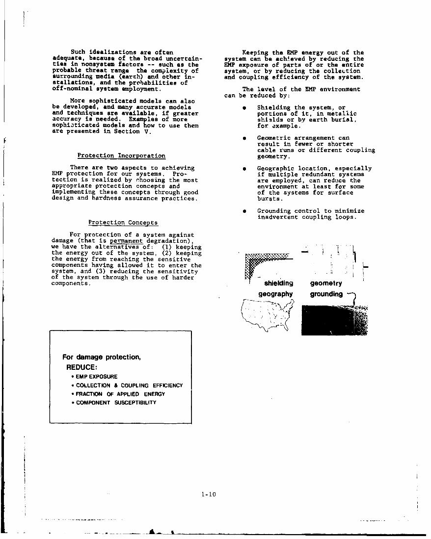
Such idealizations are often Keeping the EMP energy out of theadequate, because of the broad uncertain- system can be achieved by reducing theties in nonsystem factors -- such as the EMP exposure of parts of or the entireprobable threat range the complexity of system, or by reducing the collectionsurrounding media (earth) and other in- and coupling efficiency of the system.stallations, and the probabilities ofoff-nominal system employment. The level of the EMP environment
can be reduced by:More sophisticated models can also
be developed, and many accurate models * Shielding the system, orand techniques are available, if greater portions of it, in metallicaccuracy is needed. Examples of more shields or by earth burial,sophijticated models and how to use them for example.are presented in Section V.
• Geometric arrangement canresult in fewer or shortercable runs or different coupling
Protection Incorporation geometry.
There are two aspects to achieving 0 Geographic location, especiallyEMP protection for our systems. Pro- if multiple redundant systemstection is realized by rhoosing the most are employed, can reduce theappropriate protection concepts and environment at least for someimplementing these concepts through good of the systems for surfacedesign and hardness assurance practices. bursts.
* Grounding control to minimizeinadvertent coupling loops.Protection Concepts
For protection of a system againstdamage (that is permanent degradation),we have the alternatives of: (1) keepingthe energy out of the system, (2) keeping "jwykthe energy from reaching the sensitivecomponents having allowed it to enter thesystem, and (3) reducing the sensitivity .of the system through the use of hardercomponents. shielding geometry
geography grounding
For damage protection,
REDUCE:e EMP EXPOSURE* COLLECTION & COUPLING EFFICIENCY"* FRACTION OF APPLIED ENERGY
"* COMPONENT SUSCEPTIBILITY
1-10
*AL

The coupling efficiency of theenergy collector may be reduced by re.ducing its effective collection area.For example, one may shorten an antenna,for certain HF band or strong signal con-ditions, or rearrange equipment in orderto shorten cable runs between units. Non-conducting data transmission systems, suchas fiber optic or dielectric wave-guidesystems, are also a good alternative toeliminate the cable coupling problem.
TO PROTECT: 1'sIoPII ChILE cohIcTIO
I , ,In addition to permanent degrada-
tion (damage), there is the problem ofThe fraction of the collected erergy operational upset in many systems. Oper-
which is applied to a sensitive component ational upset can occur at much lowermay be reduced by introducing an amplitude levels than damage, and therefore requireslimiting device, such as a spark-gap, a a greater degree of protection. All offilter, or a disconnect mechanism between the concepts associated with protectionthe energy collector and the component. against permanent damage can also be
applied for upset protection. There areadditional hardware and software ap-proaches available to minimize the upsetproblem.
F!Rduce the applied energy by:
CONCEPTS FOR UPSET PROTECTION
e ALL DAMAGE PROTECTION MEASURESAM9U1Iwt SPAR¢AUN O3CONECTWEO"LOWN LItYTh4G
e HIGH LEVEL DIGITAL LOGIC
Protection against EMP may also be * CODINGachieved by choosing less sensitive com-ponents or subsystems. For instance,vacuum tubes are more damage-resistantthan transistors. Their incorporation, a HARD MEMORIEShowever, might c.eate other problems.Semiconductors that are inherently moreresistant to transient damage could, how-ever, be selected. e EMP EVENT SENSING
a SOFTWARE CIRCUMVENTION
'• l-n
----------------------------------------------- ,-t-

Using high-level digital logic, that There are several viewpcints towardis lotic circuits which have higher voltage a rational, balanced, and complete con-switching thresholds, reduces the proba- sideration o2 these "design practices".bility that the EMP coupled pulse will be The approach taken in this course is toof sufficient amplitude to result in a categorize these practices according tologic state change. The use of reason- a hierarchy of application of the practiceably long coded signal chains can further ranging from the system level (overallreduce the probability that the logic s9stem protection) to terminal protectionwould err in terms of recognizing the EMP using protective devices.induced signal as the correct signal. CATEGORIES OF
PROTECTIVE PRACTICES
* SYSTEM ASPECTScoded Dil Il iiqeM •* SHIELDING
EMP * CIRCUIT LAYOUT
ime- -
"* GROUNDING
As in the case of damage protection, • CABLINGthe use of harder components can help tominimize the upset problem. The use ofless easily upset memory systems, such as 0 PROTECTIVE DEVICESmagnetic drum or disk memories, is onetechnique. This would permit storage of In this overview section, we willimportant segments of processed infor- look at a single feature of each ofmation or portions of the program in a these for orientation purposes.memory which would preserve this infor-mation. The systems aspects are concerned
primarily with the concept of keeping theError sensing and correction codes undesired energy (in this case EMP) out
could be included in the software to of the system. As such, these aspectsfurther reduce the probability of upset deal with the control of departures fromor errors in the output data. In some an ideal system from an EMP viewpoint.cases, this is the only hardening that The ideal EMP protected system is depictedneed be implemented. in the left hand portion of the figure.
"Reality" usually involves a large numberEMP event sensing can be used for of potential "violations" in terms of
error correction or to inform system apertures, conductor penetrations, andoperators that EMP may have introduced an so forth, as depicted on the right.error. In some instances, this could beachieved automatically through the computersoftware, such as an instruction to re-process the information starting at apoint prior to receipt of the event signal. Ideal Practical
THIN SHIELD
Design Practices OPENINGS
of Protection ConceptsHEAVY. MANY-
LAYERED SHIELD
The foregoing are only protectionconcepts which must be properly imple-mented. The applicability of these con- NO PTI
cepts to any system depends on the system NOPENETRATOS
requirements including both operational .performance and environmental factors.The design practices are the practicaldetails associated with implementing the -concepts.
1-12

The circuit layo~ut aspects are close-ly akin to the systems aspects. At thesystem level they deal with the equi~pment TYPICA sIIELD'NG DE8106 W*ZoFMS.and intercabling configuration. At the CMMkm"other extreme, the circuit card, they We" Ideal with layout of printed circuit boards. WMO40M
The dominant principl1e is the avoidanc2 a.~ -FMPW Oa 4
of coupling configurations -- most nota- PM., ýpractices apply equally to large cable \, -I
systems or to printed circuit ptuckagl.s.It is generally independent of circuit Un
dimensions.
Grounding is not a panacea, norshould it be viewed as an EMP protectionpractice by itself. However, if it isnot realistically viewed, it ma makethings worse. In some nuclear testinstrumentatior systems,* controliedresistive grounds are purposely used topromote energy dissipation and to suppressground loop currents.
Here we see the most common -- andmost useless -- "ground"'.
Shielding design usually centers onpragmatic compromibes related to therealities of couistructLi-cn arzl fpbrication, GmtUftdi Is meanrngIm:economics, and applications!. renuirements. D MhWFOThese generally bni' dou.n t-)
* Wall thickness and integrity
* Apertures - "tightness"
* Penetrations -- necessary
condun~tor9.
Good shielding desigot criteria apply toall levels, that i.s o.-rall syszein enve-lope shields down to shielaiPg of indi- hMW-.6fOMvidual circuits. m1~~ieiu~.. 1u bre- V4ehrt-16)
dt 1-13
dL

Cable deal g represents an extensionof shielring and circuit practices in the
:r~i'iewpoint. It is the aree. in whichthe worst compromises are often made inthe interests of econom~y. Goed cablingcan be expensive, but V~~P coupling viabad cabling can be fatal. Here we illue-:rato thitn trend in rtblebo t~ k(rber. ima be additional shields aroundindividuaI. internal conductors, of course,which are not shown hnre). As statedprevioutrly, nonconducting data trans-
mission link3 offer a potential alterna-tive to the use of shielded cables. Their 6nTew"iapplicability must be determined basedon theisystemfpr~rformance requirements,reliab iiy of fiber optic or dielectricwave-guide systems, cost, etc.
Testi7n&
Protection verification is essential.Originally, such test methods were ad-dressed to determining whether or not
CABLING-TMO"OUTER CONDUCT09" existing s:,stems really were vulnera~ble.Today, testing is used to verify the de-
She~thl ntw~cedsign hardness Of 3ystems ot equipments.1 wa la i coui'o As important as planning and imple-IMI f testinig. The balances between laboratorydoSmctric sI~triCO *doelctr~r tests and full-scale simulations, and
ScorMwioeo brd ST~~tr between component and full-system tests,BAD TTER BESTdepends on many factors, such as system
size, probable threat situations, unavoid-able susceptibilities, and so forth.
-A)N stdesProtective devices such as surge
arresters, filters, and circuit breakersare generally used after the other aspectshave been applied. It is not possible tokeep all the coupled energy out of the Isystem. These terminal protection de-vices are to further limit this residualenergy at the terminals of equipmentsemploying sensitive components or circuitsrfrom either damage or upset.
1-14

The reasons for testing are sunma-rized below:
Why Test?
0 Verificetion of analysis
* Extention of analysis
* Surprises
0 Quality assurance
* Certification
Testing, in some cases, is for the A final test of the complete system,purpose of ver-ifying analysis and the de- in a fu'iscaleiimulator, is a desirablesign of our systems. It provides confi- goal. But, at present, this is sometimesdence that what we did was correct. On impractical, for example, in an extendedthe other hand, due to the required simpli- communi•ation network or free-fieldfying assumptions used in the analysis illumination that has to be augmentedphase, the test phase reveals obscure with direct pulse injection techniques,coupling paths or system degradation (sur-prises). Finally, testing provides up ameans of assuring the quality of the endproduct and for production control. 1.5 PROGRAM PLANNING
To illustrate the need for testing, W is a system problem and, there-several typical surge protection com- fore, must be considered on a systemponents were tested. EHP waveforms, having basis during all phases of system design.very fast rise times, short durations,and high peak voltage, were applied in-stead of the usual test waveforms based onlightning or other more common surge-testrequirements. In the cases of two of theprotection approaches, the data sheet Consider EMP in all phaes:ratings were not exceeded by the EMP test aoncept prototypwaveforms. In all cases, these protectioiucomponents were destroyed. High current,fast rise-time pulses can be applied di- Wrectly to the circuit being tested, using dreelment procaotitoa high-power pulse generator. Such labtests can add assurance that the system M INIO lumE n. Ewill pass full-scalQ simulation tests.
A simulation of the radiated EMP details _ maenvironment can also be created (see ,,.Section VII). For example, the ARES simu-lator is built as a very large trans-mission line and produces EMP-like fieldsin the space between the towers,
1-15

The specific management approacher .... Ito EMP for any given system will depend Ion many factors -- people, fun•s, eqiiip- EMP sA c qALLnGc, , l AG cMNT •r oLEm iments, existing organ4 .zational structure --
but must be considered at all levels.Manaaement must have visibility of the * Uncrtoint•es of AnalysesEMP control program and provide authors-tative direction fnr resolving conflicting * Difficulties of Testim
requirements. * Sol-rf- Art
e Limited Focifitles
e Personnel Troaning
0 Total System Life
Part of the challenge is the state-of-thc-art. The c'irrently availableinformation, as exemplified by the Hand-books and other references in the area,is directed primarily to a discussion ofthe EMP phenomenology, electromagneticinteraction, hardening concepts and imple-
EMP considerations at the system mentation guides.level are concerned initially with threatdefinitions, and establishing the pro- The more developed electromagnetictection philosophy. As the program pro- interaction areas, such as radio frequencygresses, management is concerned with interference or lightning, have availablereview of the hardening program at the commonly accepted design nomog-ý.aphs andsystem and subsystem levelse, and insuring charts which can be used reliably tothat the hardening is properly incorpo- select components or implement designs.rated.
This "technology base" for RFI andlightning has taken many years and millionsof dollars to develop. A similar develop-
nTASL. ment has yet to "mature" for the EMP01111111M problem area. As a result, the currently
A available information must be translatedinto the specific needs of the EMP harden-ing plan. This will take money, people,
nT=ALU AND SSTAUtSt and training time ror this purpose. InP SVST§MIYTM4ITSLO
Tsr ,Mu other words, there is no easy way out: atMING %, the present time.
PAOOAMS urnl Avoilabl. !normaloiti
Plienomenology Cwplg Rtmmse 4Hdor ing Concepts ExamplesIn
Interaction invernetation Guidets
FPP is a challenging managementproblem. Uncertainties regarding ana- $+'IO T,,.n Timelysis and testing are the basis for thischallenge. More important, the state-of- T,.saethe-art of EMP is still evolving. Timeand funding allowances must be made for FI.s Nomograph%, Charts, Conients, Hardening Plan, Test Plan,adequate personnel training. Lastly, as Maintenance Plan, Constr,:'on Guide, How-Too. Do-I Cook Books,reiterated previously, EMP must be con- Specificohos, Test Piocedurst, Quality Control, Modificationsidered for the entire life of the Procedures, Field Pelsonnel Troining, Retrofit Controlsystem,
I - I

An adsquate base of personnel quali- One of the major challenges to man-fied to handle EMP problems often does agement is meeting the funding require-not come easily. Man&gSvagnt Jhodls -on- r'ntq to provide adequcte hardening. Insider a planned education period for the many cases, this can be don durit,g chetraining and education of personnel. Past initial program planning phases. If thisexperience has indicated at least one to is not always possible, especially for atwo years of direct involvement is required program in being, one approach has beento develop a capability for adequately the so-called hlroware trade-off approach,dealing with EMP interaction and hardening which trades off a large number of systemsproblems. of unknown survivability for a somewhat
smaller number if systems with assuredIn addition, this training period survivability.
should allow for a few mistakes. Onesuch approach is to initiate the EMP hard- Another approach has been to minimizeening efforts with what might be termed the need for hardening for the close-ina "test-bed" program. During the course source-region threats by employing geo-of this test-bed program, the necessary graphic dispersal and increasing theanalysis, testing, and hardening are de- number of systems somewhat.veloped in terms of a consistent!y fundedand well-laid out effort. Another approach can consider mini-
mizing peacetime reliability costs andconverting the dollar savings into as-sured survivability.
PERSONNEL CHALLENGES
" Planned Capabilities Development
" One To Two YearsMEETING THE $ CHALLENGE
0 Plan For A Few Mistakes_______________________________________Program $ Initially
OR
Trade-Off Large Number Systems of Unknown
Hardening a system against EMP is FORnot a one-time effort. EMP protection SomwhatSmallr Number ofSysemsWithmust be considered from the time of in- AsuredSurivabilit.ception throughout its life cycle. Ifthe system is to remain hard, EMP controlmust be exercised during the productionand operational phases including controlof all modifications.
S' •'-- •• In general, the bulk of EMP hardeningP.- .CW costs are roughly independent of tte re-
quired protection level, once the decisionis made to protect. Typical EMP harden-ing costs (if incorporated early) forstrategic systems can be on the. order of*
_a few percent of the system cost. Ifretrofitted, costs can easily rise inexcess of 10 percent of system cost, tonearly the original system cost in somecases.
1-17
AL

at the lead laboratories of the Army,Navy and Ai: Force. These large-scalefree-field simulation facilities are
/minimum constructed, maintained and operated byprotection DFA, and the three services' lead labo-
ratories.
effects, In order for management to establish,s /MP review and control an EMP program, es-
pecially for large complex systems, theymust have a formalized reporting structure.These reports have often been denoted as
' * e "White Paper" and assessment reports.protection level
minimum nuclear maximum nuclear Identifying the nuclear weapon*threat levels (source region) threats to the system in context of the
threat levels mission of the system is often called a"White Paper".
Delineation of these threats deter-mines the resulting EMP environmentswhich must be considered.
subsystemdesign primegroups contractor
Management must also provide for the t tnecessary equipments tc conduct the EMP weapon likelihardening program. Typical equipment re- threat definition of nuclear targetingquirements for a complete EMP hardening study effects on systemr- circumstancesprogram would range from computers, lab- (intelligence) (inteligenc.)oratory impulse test equipment to large-scale simulators.
systemperformancerequirements(user)
The assessment reports initiallytranslate the DIP threats in terms ofthe testing, analysis and hardening re-quirements. Later on they can be used toreview progress toward achieving an EMP-hardened system.
ASSESSMENT REPORTS
PERIODICALLY INDICATE STATUS IN:
Contractors (both prime and, in somecases, subcontractors) could be expected 'HARDENING CRITERIA AND IMPLEMENTATIONto possess or have access to the neces-sary computers to conduct the requiredanalyses. Depending on the complexity of 'TESTING
the test requirements, contractors couldbe expected to have at ;. ast limited labo- 'ANALYSISratory test setups, For the more complexsubsystem type tests, sophisticated labo-ratory and field testers are available
1-18

On the basis of past experience, itis suggested that careful review of theEMP program be periodically conducted for'ossible trouble areas, such as preo~ccu-pation with one area, for exauple, shield-ing or terminal protection, at the expenseof other areas. Above all, the EMP pro-gram must have good visibility and manage-ment.
The EMP hardening features must be s $ 1 $maintained during production by proper
AJ
quality control and during use by edu-cation and training of personnel, as wellas by periodic inspection and retesting.
While many of the program planning EMP System Vulnerabilty Lead ab Consultationaspects are self-evident, the most im-portant are summarized here.
"stre• A library is maintained by DNA-definitin DASIAC at G.E. Tempo In Santa Barbara,
visible California which includes most of theEMP organization L ana"s report documentation. A computer pro-
gram library is maintained by the LawrenceLivermore Laboratory, Livermore, Cali-EMP .C. EMP __fornia under DNA funding. Data files
education Noble ~ I~r~rt&~naintenance optm o pote tiog (computer storage and retrieval) on semi-conductor and component damage levels,a= /R computer programs of special nature, and
f technical libraries are also maintainedat the service lead laboratories.
tetfacilities Both inalytical and empirical Lp-
proaches are ,required to realize a hard-ened system. Neither can be exclusivelyrelied upon. The number of uncertaintiesand unkno'.Ls is so large that one approathis often used to confirm the results of
1.6 STATE-OF-THE-ART the other approach.
Today, the stace-of-the-art is con-sidered to be sufficiently advanced topermit the cost effective hardening ofmost military hardware with a high assur-ance of acceptable EMP hardness level.The information that is available is in a LIMITS of ANALYSISform to provide guidance in the designand implementation. The answers tospecific questions are not generally LIMITS of TESTINGavailable if programs have not been inexistence to attack them.
A number of information sources areavailable, such as the DNA handbook, ser-vice laboratory handbooks, DNA ProtectionEngineering and Management Notes, AFWL At the present time, our analyticalNote series, technical reports, specific capability is sufficient to assess thesystem reports, and so forth. EMP hardness of systems and to design
future systems EMP hard with reasonableconfidence. There are still limitations,due to the assumptions we must make, toour analytical capability so that we muststill reply on testing to verify the ana-lysis and uncover obscure problems.
1-19
'" " .... ' "~~~~I ' '• ' ' ' ; •

The specific EMP response is highly a test specimen is not available, suchdependent on obscure details not gener- as during the design phase, so analysisally controlled during manufacture or is the only available tool.design (such as the type of corrosionprotection employed, extraneous couplingpath, etc.) Furthei., the number of de-tails important in the electromagneticinteraction seuise can be quite large.For example, typical electronics sub-systems may have as many as ten thousandpotentially susceptible electronics com-ponents and related coupling paths. Theelectrodynamic analytical techniques areamenable only to fairly simple structures TESTINGand limited number of components. Speci-fic component responses cannot be ana- CAN: validate analytical approacheslytically modelled because much of the confirm design
basic information has yet to be developed. develop component subsystem susceptlblllty
reveal obscure electromagnetic details 'or compact systemprov'de flial quality assurance
CANNOT: relate test method to threat
determine if tests are properly wriducted
economically test widely dispersed systemstest for many "source region" threats
WITHOUT RESORTING TO ANALYSES AND STUDIES
ANALYSES AND STUDIES
CAN: find problem areas
identify likely areas of weakness
provide design assurance
guide test approach selections
confirm test res"lts
CANNOT: identify specific levels of vuinerability or
susceptibility for a complex system
find specific weak pointsselec, more or less susceptible components
WITHOUT RESORTING TO TESTING
Like other electromagnetic problemsin RFI (Radio Frequency Interfer'ence),HERU-CHaiardous Electromagnetic RadiationE-F-ects on Ordnance), or TEMPEST-(Compro-mising Electromagnetic Emissions fromSecure Communication Equipment), empiri-cal testing is required. However, an ex-clusively empirical approach has obviouslimitations because the very act of makinga measurement can upset the test andintroduce extraneous data. Further, test-ing alone can become very expensive ifall aspects of system hardness must bedeveloped experimentally, especially forwidely dispersed systems or for systemswhich must survive above ground withinthe source regions. Finally, many times
1-20

1.7 SUIMMARY The rEt.' of the course will pro-vide a more detailed and technicalinsight into how to carry out an EMP-
In summary, the EMP from a high- hardening program.altitude burst can affect substantialfractions of the earth's surface without It is designed to provide an aware-significant contributions from other ness of the various approaches whic-Eweapons effects. The waveshape, field m-1-gt be used for your system.intensity and spectral content of thepulse are unlike those normally experi- The various "tools," analyticalenced due to man-made or other natural or experimental, will be discussed andsources. their advantages and limitations pre-
sented..Hardening to EMP from a high-alti-
tude burst must be considered for almost A few examples will be given onall important systems, even though other how these "tools" may be used.weapons effects may not be important.
But we cannot make "experts' over-The EMP from a surface burst is night, nor will attending this course
more restricted spatially. It has an provide all of the answers you need.exceptionally large and abnormal wave-shape within the source region. Withinthe source region (or near to it) wherethe EMP poses a major threat, the othernuclear weapons affects must also beconsidered. The system must possess"Balanced Hardness" with respect to theother nuclear weapons effects of blast,thermal, radiation, etc.
Based on somewhat scattered datadeveloped during the period of atmos-pheric testing and extensive informationbased on thorough analysis and experi-mental simulation, EMP can cause function-al damage or operational upset, especiallyfor the more sophisticated systems em- THE ENGINEERING COURSEploying transistors or those highly de- WHICH FOLLOWS WILL PRESENT:pendent on digital computation. Todayelectrical and electronic systems can be ,WHAT "TOOLS" ARE AVAILABLEprotected. The cost of this protection *WHEN THESE MIGHT BE USEDwill vary with the nature and mission ofthe system. The most economical and 'HOW TO USE THEMeffective protection is realized if thehardening effort is considered earlyand made an integral part of the systemdesign.
System@ CAN be protected
costs vary but it's Lest tobegin at the5"gnning
--- I- J1-
'f 1-21

SECTION II
INTRODUCTION TO THE TECHNICAL COURSE
As an introduction to the technical As a consequence:portion of the course, the objectives ofthe course and the content of the course * There are no easy, optiv.'-m, orwill be stated. Further, some basic cookbook approaches which areelectromagnetic principles, which are im- applicable to all systems. To-portant for understanding what will be day, each system is treated ascovered subsequently, will be reviewed, an independent entity, usingFinally, some EMP ard system character-. past eftorts for guidAnce.istics which are referred to throughoutthe course will be defined and discussed. * There are no universa': -arden-
ing techniques or devi,. +_ whichappLy to all cases. The re-quired protection for each case
2.1 COURSE OBJECTIVES must be determined based on thethreat and the mission require-
The overýll objectives of this course ments.are to provi-1, -n awareness of what EMPis, what 1s,.kpact on systems may be, . There are no optimum analyticalwhat tools are available to assess the im- or test approaches for all cases.pact on c&ystems, and how to protect against These must be deterniined basedthe effects of EMP. on the system configuration,
complexity, goals of the program,Many of the answear;; are still being and costs.
worke' out for particular systems appli-caticns in regard to the: Hence, we will present to you several
approaches to the EMP problem. We hopeMethodologies to provide enough background to enable
you to select the "best" combination forAnalyses your needs.
Protective Techniques
Test Techniques
Maintenance
These answers are in a state of evolution.
There are No lesy Answers
No "Ove end Only"IMP Hirigalmi Is a D Vf.t Problem Right-Way
Get#nees Amswers
Aenls ?[Pmeteftis Toelenlm ?Tot Tisbiqss ?Alieteman The course can only reflect the
state-of-the-art; so do not expect tocome away from the course loaded with"nomograph-chart" solutions, "c:okbook"formulas or standardized approaches whichcan be bripfly reviewed and routinelyapplied to your system.
2-1

We hope to tell you something aboutthe problem, what "tools" are availableto help solve the problem, the limitation In rhree Days We Can Only Hit the Highand advantages of "the tools," what the Points of a Multi-Disciplined Problemhardening concepts are and how to applythem, and how some people are approach- Nuclear Physics Program Managementing the overall problem. We hope thiswill be sufficient for a first-cut assess-ment planning effort to formulate programs Applied Math Design Practicesfor dealing with the EMP problem. Ex-amples to illustrate these will also Field Theory quality Controlbe given.
Circuit Analysis EM Maintenance
Field Measurements Operational Training
What to Expect? Teat Simulation
The State-of-the-Art.
"* Concepts
"* Methodologies
"* Tools 2.2 BASIC ELECTROMAGNETIC PRINCIPLES
"*Applic ti To adequately describe or character-Arpplications ize electromagnetic phenomena in nature
(in this case the EMP phenomenon), re-"* Examples quires familiarity and understanding of
some basic field quantities. These fieldquantities are listed below along withtheir units in the rationalized MKSsystem of units as a review.
In three days we cannot turn youinto EMP specialists.
We do not intend to teach you basicmathematical processes, such as Fouriertransformations, how to program SCEPTRE, ELECTROMAGNETIC FIELD QUANTITIESor other computer codes, etc.
We are not going to make you into a ELECTRIC MAGNETIC
nuclear physicist, simulator designer,or high-voltage specialist. EME Electric Field N •: Magnetic Field
You yourselves will have to apply Intensity Intensityand enlarge your existing skills to the (Volts/i) (amps/m)EMP problem based to some extent uponthe suummary of all the di'sciplines, skills Electrc Flux Magnetic Fluxand approaches presented during thecourse. (coulombs) (webers)
In the three days allocated to the E ca i
"EMP" Awareness Course," we can only hit 0 I Electric Flux 8 D Magnetic flux
the high points of a multi-disciplined Intensity Densityproblem. References are provided to (coulombs/m2 (webere/m2)assist you in your future efforts andapplying the information and tools whichhave been developed.
2-2
A.

It is essential to keep in mind thatin a time varying el!ctromagnetic field,the ele tric field (E) and the magneticfield (H) cannot be created independently.Coexistence of the electric and magneticfields is a prerequisite to the establish- Relationships Between Fieldment of an electromagnetic field. At low Perametereoft te Medium Quantities and Parametersfrequencies (Z 10 kHz), the electric and of the Medium
magnetic fields are often considered sepa-rately for simplification of shielding 4 9 eu sianalysis and design. At these low frequen- .Pawm.cies this is a very good approximation.True separation of these fields only ex- -. Permeeli•v I-ists in the static (dc) ase, however. (Ho.yn
r. ConductivitV 0J 4 s"CMhoSMA)
Coupling of Time-Varying
Electric and Magnetic FieldsElectric fields are the result of
charge separation in the media. For
Charge simplicity, consider the generation of a
Static Fields static (dc) electric field. A simpleCurrent- H case is that of a parallel plate capaci-
tor, Impressing a voltage (V) acrossthe plates results in a redistribution
(Charge------- of charge on the plates as shown. ThLiTime-Varying redistribution oj charge results in an
Fielde Current--- H electric field (E) between the plates.I_.The relation between the electric field
and the applied veltage, in this case,is given by:
Y volts/meter
The relationship between the electric
and magnetic field is given by:
= •Generation of an Electric Field
in a Parallel Plate Capacitor
whereConducting Plate
T = characteristic impedance ofthe media
4-4- +4T)0= 377 Q is the characteristic I I+
impedance of free space. /L
The medium also plays an importantrole in formulating the electromagnetic i n
field. The parameters of the medium pro-vide the necessary link between variouselectromagnetic quantitie3. The moreimportant medium parameters and theirunits, and the rcle they play are indi-
A• cated here.
2-3
IA

If we have a force which causes volume. These are shown in the figure.charge separation, an electric field is The concept of current density is use-created. In this case, the force was the ful. For an incremental volume or area,applied voltage. For example, in the the current is uniform throughout, andcase of EMP generation, as we will see in the current is related to the currentSection III, the force causing the charge density by:separation is the nuclear detonation andthe resulting gamma rays. V
The generation of magnetic fields =
requires current to flow. Again for sim-plicity, consider the static (dc) case. whereConsider, for a simple example, the fieldbetween two current sheets carrying a = ototal current I. The total current isrelated to the current density (J8) by V - Lthe relation L
I = JsS G
where a = conductivity of the materialcross sectional area of the R = resistance of the material
current sheet. for the incremental volume
This assumes a uniform current density = induced electric field.which holds only for the statij case.The resulting magnetic field (H) betweenthe current sheets is given by;
2-U amps/meter.
In L case of EMP, see Section III, thecur_-,it flow results from the interactionof the gamnmas produced by the nuclear Ohm's Law for an Elemental Volumeder-nation with the media.
I - V -conductivity =
G e n er b i n o f e M ag ne e t ic F i e ld M otw ee n C u r r e n t S h e et s s - - a
joaE R= L0-
In many cases in field theory, theevents occurring at a point, or withinan incremental volume, are of interest.In these circumstances, it is desirableto define the relationships between thecurrent and voltage for the incremental
2-4

Direction of power flow in a distantEMYfield is given by the POYI4TING vector'an~dfcanl'be obtained by use of the right- ----- -20hand rule, as indicated. Note that thePOYNTING vector, P, gives not only the 40i
direction of power flow but also the powerdensity of an EM field in watts/rn2.
O~Ejn~-----------------------
01rotiaui of P*~ glow for a RedLbftd 9M Wave to
S. .. " ..
.. . .
... ...
... ...
L LiJ.A
I
th•
(S,
VGENERALIZED HIGH-ALTITUOE EMP ELECTRIC
P. Poyntk / Vect)r AND MAGNETIC-FIELD TIME WAVEFORMtwattam/m')
-In.tkn of Powsw F~ow Equally important, in order to de-termine the coupling to a system, is thepolarization of the wave. The polari-zation is defined ol the basis of the E
__ field vector. Vertical polarization iswhen the E field vector is normal to thedirection or propagation and wholly with-in the plane of incidence Horizontal
2.3 !MP CHARACTERISTICS polarization is when the t field vectoris normal to both the plane of propaga-
The waveform of the EMP plays an im'- tion and the plane of incidence.portant role in the coupling to systemsand the effects on systems. At this time The angles of incidence are thewe will define the more important char- vertical angle (*) between the point ofacteristics of the Ei'4P to serve as a base observation and the burst point measuredof understanding for subsequent discus- from the location of the point of obser-sions. vation, and che horizontal angle (e) be-
tween the axis of the energy collectorTwo of the most important parameters and the direction plane of incidence.
are shown in the figure. The rise time(tr) is defined as the time between the10 and 90 percent points of the leadingedge of the wave. The time to half-valueis the time for the wave to decay to halfamplitude on the trailing edge of thepulse. These times determine the spectral Burstcontent of the wave.
Antenna Direction Of Incidence(Collector)
ANGLES OF INCIDENCE
2-5

Other important parameters of the For larger structures, the generalEMP are the power density w/ml) which case, the collection area and efficiencygives the total energy contained in the must be defined. This is a function ofpulse, the power flow which was defined the system size and configuration. Thepreviously for an EM wave (i.e., the important aspect here is that, in gen-POYNTING vector), ftnd the relationship eral, systems cannot be considered asbetween the I and R fields (i.e., the small structures over the very largeintrinsic impedance of the wave n - / frequency spectrum of the EMP. Conse-quently, to determine how much energy iscoupled to the system, the response ofthe coupling structure or collector at2.4 SYSTEM/EQUIPMENT CHARACTERISTICS all frequencies in the spectrum of theEMP must be determined.
The characteristics of a system/sub-system/equipment from an EMP viewpoint Other ways that energy enters aare those that influence (1) how the ener- system are through penetrations th!"oughgy enters the system, (2) how much energy the enclosure. These penetratic••s areenters the system, and (3) what effect such things as holes in a shield* (con-this energy has on the system. ducting enclosure), cable entries, or
other conductor entries (such &s waterInsofar as EMP coupling is concerned, pipes, etc.).energy coll ction by the system can berelated to E field coupling (linear an- How much energy enters the s•ytemtennas or collectors), H field coupling and arrives at sensitive portioivs of the(loop antennas or cable loops), or through system is determined by the transferan intermediate conversion impedance (Z ), function of the system. The transfersuch as the earth, where the pickup is C function is the ratio of the output ener-sometimes directly proportional to the g versus the incident energy as a functionapparent applied fields. These coupling of frequency.modes apply to both exposed collectorsor collectors inside shielded enclosureswhere the fields are reduced due to theshielding. Examples of these couplingmodes are shown for the simpl*fied caseof small structures (small compared tothe wavelength of the highest frequencycf interest, or less than about 2 feetin length or diameter for a typical EMP SVSmegIUebohIIPwaveform).
laP CONpili, ,
C.
E
A LEt
/ ~~'Ilk- Once the energy reache3 a sensitiveSportion of the system, it may result indamage or upset. Damage is defined aspermanent degradation of the system, suchas com onent burnout. Upset, on theother hand, is defined as the temporaryimpairment of thu system, sLch as circuitbreakers tripping or memory erasure incomputero, this results in a functionalimpact,
2-6

2.5 SUMIARY
This section has served as an intro-duction to the EMP problem and preaentssome of the important characteristics ofthe EMP and systems. Further, it pro-
RM wn*andUpwo vides some basic knowledge of EM princi-ples which are required for understandingthe discussions.
Systems are often referred to as be-ing vulnerable to EMP. For a system tobe vulnerable to EMP implies that due toits response to the EMP stimulus it canno longer perform its mission.
System hardness is another term whichshould be defined. The hardness level ofa system is a measure of its vulnerabiuityto the EMP. To say a system is hard im-plies that the presence of EMP will notadversely affect the performance of thesystem.
System protection (as used in SectionVI) is defined as the measures (fixes)employed to render the system hard, (thatis, protect the system against the effectsof EMP).
2-7
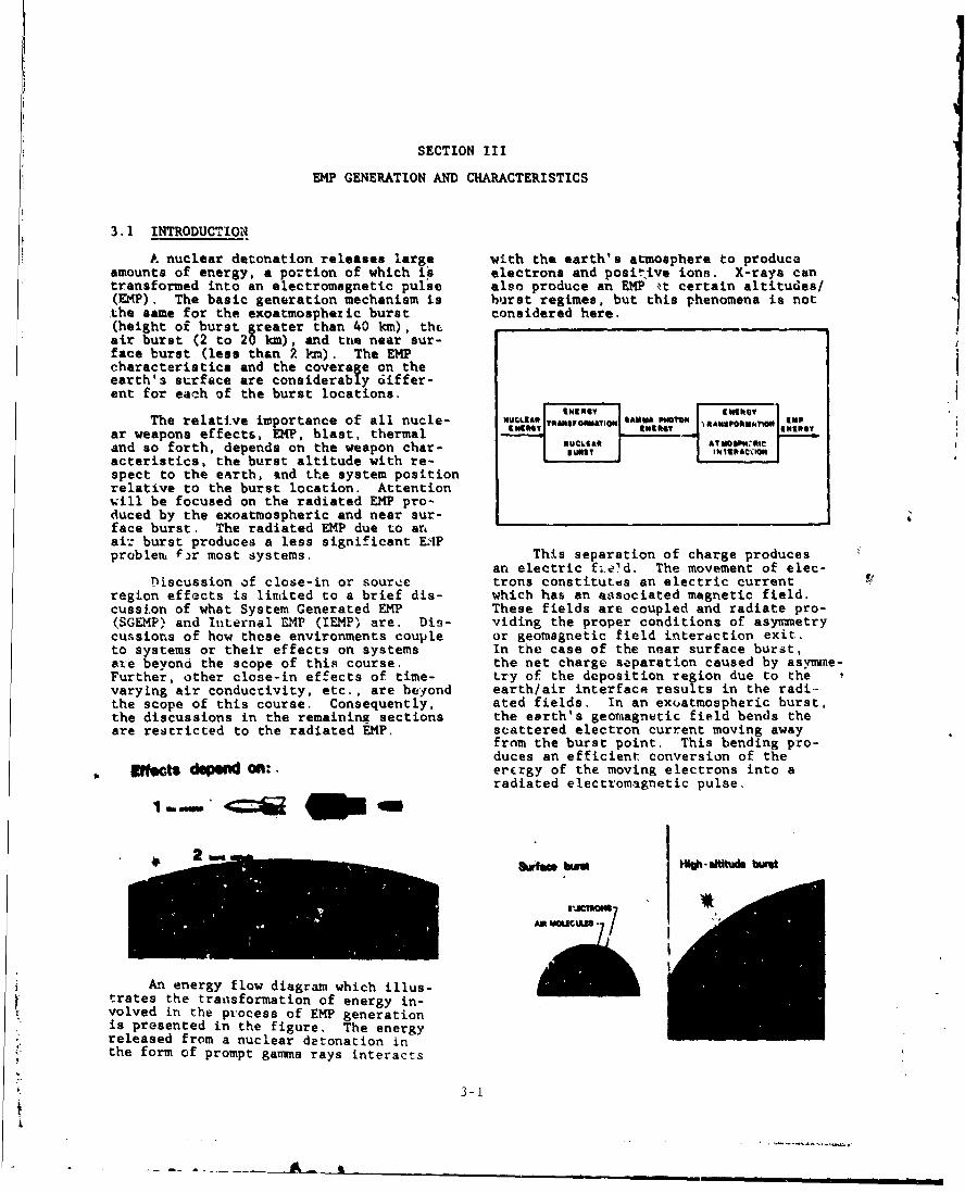
SECTION III
EMP GENERATION AND CHARACTERISTICS
3.1 INTRODUCTION
A nuclear detonation releases large with the earth's atmosphere to produceamounts of energy, a portion of which is electrons and positive ions. X-rays cantransformed into an electromagnetic pulse also produce an EMP 't certain altitudes/(EMP). The basic generation mechanism is burst regimes, but this phenomena is not.the same for the exoatmosphezic burst considered here.(height of burst greater than 40 km), theair burst (2 to 20 km), and tthe near sur-face burst (less than 2 kn). The EMPcharacteristics and the coverage on theearth's surface are considerably differ-ent for each of the burst locations.
The relative importance of all nucle- NUCLEAR p&NSIM• °.10°. P ampar weapons effects, EMP, blast, thermal ] SWISS, IWIRSYand so forth, depends on the weapon char- RUULIAR ] ,WI©acteristics, the burst altitude with re-spect to the earth, and the system positionrelative to the burst location. Attentionwill be focused on the radiated EMP pro-duced by the exoatmospheric and near sur-face burst. The radiated EMP due to anaiz burst produces a less significant EAPproblem fr most systems. This separation of charge produces
an electric f&eld. The movement of elec-DLscussion of close-in or source trons constitutes an electric current
region effects is limited to a brief dis- which has an associated magnetic field.cussion of what System Generated EMP These fields are coupled and radiate pro-(SGEMP) and Internal EMP (IEMP) are. Dis- viding the proper conditions of asymmretrycussions of how these environments couple or geomagnetic field interaction exit.to systems or their effects on systems In the case of the near surface burst,ate beyond the scope of this course. the net charge separation caused by asymme-Further, other close-in effects of time- try of the deposition region due to thevarying air conductivity, etc., are beyond earth/air interface results in the radi-the scope of this course. Consequently, ated fields. In an exuatmospheric burst,the discussions in the remaining sections the earth's geomagnetic field bends theare restricted to the radiated EMP. scattered electron current moving away
from the burst point. This bending pro-duces an efficient conversion of the
gffect depen On: ercrgy of the moving electrons into aradiated electromagnetic pulse,
1.... Omm . ' "
Swfam bu*H - iWft~s bss"
An energy flow diagram which illus-trates the trainsformation of energy in-volved in the process of EMP generationis presented in the figure. The energyreleased from a nuclear detonation inthe form of prompt gamma rays interacts
3-i

For both the high altitude and sur- The size of the deposition regionface bursts, intense fields appear in ia confined by the atmosphere for thewhat is called the deposition region. near surface urst. However, the pres-The deposition region for a surface burst sure pulse which causes structurai dam-is limited to about a two tc ten kilo- age, is not similarly restricted but ismeter diameter about the burst. For a instead proportional to the weapon yield.high altitude burst, the source region Thus, in the case of soft systems fromcan be or, the order of 3000 kilometers an overpressure viewpoint, the most se-in diameter. This deposition region ex- vere EMP exposure at otherwise survivabletends from about 20 to 40 kilometers in contours is associateo with the low-yieldaltitude. In the deposition region, near surface burst. If weapon systemsweapons effects other than EMP (such as have high overpressure survivabilityradiation, blast, thermal, etc.), must criteria, then close-in EMP for surfacealso be considered, bursts must be considered.
The electric field in the depositionregion can be in excess of 100,000 volts/meter. Less intense fields appear out-side the source region (the radiatedfields). The maximum fields on the earth'ssurface due to an exoatmospheric burst LOW ylekare of the order of 50,000 volts/meter.For a near surface burst, the radiatedfields utaide the deposition region canbe on the order of 1000 - 5000 volts/meter. The radiated fields from the air 4burst are less intense than the citedcases due to the near symmetry of thedeposition region. af A I.•
The radiated EMP has a fast rise IMP ttime and thus has a spectrum which occu-pies a major portion of the communicationsand. Significant spectral energy is
present in the exoatmospheric EMP overthe frequency range of a few kilohertz cc100 megahertz.
In the case of an exoatmosphcric Another nuclear weapon effect oftenburst, a significant overpressure pulse confused with EMP is communications "black-does not exist near the surface of the out". This effect also results from theearth. Almost all of the other prompt ionization of the atmosphere due to theweapon effects are diminished by the nuclear detonation. In the ýase ofatmosphere, so that the most significant "blackout" this ionization affects theprompt weapon effect is the EMP. As propagation path, that is, it changesnoted previously, the source region can the effective height of the ionosphei.ebe quite large, in the order of 3000 km or increases the attenuation, such thatin diameter. As a consequence, the radi- effective communications are lost.ated fields from this source region can "Blackout" does not interact with thecover a substantial fraction of the earth's ttrminal equipments resulting in damapesurface, or upset as is the case with LMP. "Black-
out" is also a late-time (seconds tohours) effect; EMP is a prompt effect,"Blackout" will not be considered furtheiin this discussion.
3.2 BASIC ATOMIC AND NUCLEAR PHYSICS
To understand the basic energy trans-formations from nuclear energy to EMPenergy requires a review of a few basicfacts from atomic and nuclear physics.The discussion which follows will con-sist of a review of atomic structure andenergy levels within the atom, nuclearfission and Lhe nroduction of gamma rays,and the interaction of the ganina rayswith the atmo:•phere and the conditionsfor radiation of electromagnetic fields.
3-2

The struct ure of an atom can be visu- Atoms and nuclei exist in statesalized in the familinr form of a small, having certain discrete energies. Thispositively charged nucleus surrounded by is the basis of the quantiffn theory de-an electron cloud. The electron cloud is veloped by Bohr, Planck, and many others,held in place by the electric coulomb at- This theory gives a complete explanationtraction between the nucleus and elictrons. of chemistry and atomic phvsics. ThereThe nucleus is on the order of 10- cm can be no doubt of its essential correct-in diameter, while the electron cloud is ness.about four orders of magnitude larger. The energy difference of electron
levels is of the order of a few electronvolts. An electron can fall from onelevel to a lowar one, at the aame timeemitting a quantum of litht (photon).
TAM * The energy lost by the electron is carriedaway by the light quantum. For example,"green" light quanta have energy of about2.5 electron volts. An electron volt is
Id.died& Wi I the kinetic energy gained by an electronPh" by-n when it is accelerated through a potential
ndm muMsd of one volt.
•_16 BEC OM Y MEVRS M AN A7OM
oect__f_----------mf--
The nucleus is made up of protons __ " e.. rt. k e teIu|(single positive charge) and neutrons et o /(zero charge). The nucleus is held to- in it / IW Itemgether by intense, short-range forces gro.dv levele(nrmal stetowwhich are not yet completely understood.These nuclear forces are so strong thatthey ove-balance the electric coulombrepulsion of the pcotons for each other.
The energy difference of protonlevels in a nucleus is of the order of afew million electron volts. A proton ccnfall from one level to a lower one, atthe same time emitting a gamma ray (photon).Again energy is conserved. There is nodifference between gamma rays and light
P electric force quanta except that gamma rays have aboutW 4F a million times more energy per quantum.
muclear force Gamma rays are the principal cause
/ of radiated region EMP. About 0.1% of0, the energy of a typical nuclear bomb ap-
pears as prompt gamma rays. How doesthis happen? Let us consider the fission
m.os " 0 process in order to answer this question.
3-3

PROTON ENERGY LEWIS N A NUCLEUS
. . . -crkp__ pote tionparoton fre
Proto -&od zero omoflyaf.w. Mllom volts .
10 modes -K 9 ground level (mormul state) I N"• IPoteotiel of N *•q- ~~neclear force "•N
The protons in a nucleus repel each We will now consider the concept ofother electrically. in a spherical nil- a chain reaction. On the average, a freedcleus the electric repulsion is over'-Al- neutron travels about 10 cm before strik-anced by the nuclear forces. Ordinary ing another U2 3 5 nucleus and making itnuclei are held spherical by asurfac, fission. If the piece of U2 3 5 is tootension. small (sub-critical) the freed neutrons
will escape without causing further f is-In large nuclei, the surface tension sions If the piece of U235, is largc%
is not strong enough to keep the nucleus (super-critical), the number of fissionsspherical. The electric repulsion tends will grow exponentially with time, withto make the nucleus elongate, eventually the number of fissions proportional todividing into two roughly equal parts. et/T. The enfolding time T is approxi-This is the fission process. This is one mately equal to the travel time of aof the basic reasons why nuclei larger fmd neutron before hitting anotherthan uranium do not exist in nature; they U nucleus. This time is in the orderare unstable against fission, of 10 nanoseconds. The EMP can have a
comparable rise time.
Where do gamma rays come from? Th6fission fragments are usually not born
FISSION OF LARGE NUCLOi in their ground levels, Free neutronscollide with other nuclei in the bomb orair or earth, knocking some of these in-to levels above the ground level. Gammarays are then emitted in transitions backto the ground level.
force
k"o lmonto
Some nuclei, like '.235, are just on 0the verge of being unstable, If such anucleus is hit by a free neutron, it mayundergo fission. The fission process isnot neat and tidy as a few free neutronsget lost in the rush, These freed neu-trons may hit other U2 3 5 nuclei, causingthem to fission.
3-4

How do the gamma rays cause EMP? Deposition Region FieldsThe answer is through the Compton inter-action process. Compton discovered that The gamma rays emitted by the nuclearphotons can collide with electrons, knock- detonation are nearly symmetrical, anying them out of the atoms in which they anisotropy of the emission of the gammaswere originally bound. These Compton col- is small and of short duration comparedlisions are somewhat like the collision with other factors. The result is theof a moving billiard ball with one at rest. Compton electrons created move radiallyThe recoil electron, like the ball origi- away from the burst point and there existsnally at rest, goes predominantly forward a radial symmetric current distribution.after the collision. Thus, a directed The scattering of the electrons leavesflux of gamma rays produces, by Compton behind the heavier positively chargedcollisions, a directed flux of electrons. parent molecule. This separation ofThis constitutes an electric current, charge produces a strong radial electricwhich generates the EM?. field as shown in the figure.
Er
l COWMPTOU• U
Thdsg hr Csm phosatkr Prums.
aEm
CHARGE SEPARATION MODEL
For this symmetrical condition, nomagnetic field is generated and there-fore the deposition region fields are non-
We can now consider some order of radiating fields. In the depositionmagnitude estimates of the energy involved region in early time, the Compton electronat each state of the EM? generation pro- current dominates and the radial electriccess. A one megaton bomb releases 4 x 10¹⁵ field rises rapidly. Due to additionaljoules of energy. About 0.1% of this en.- collisions, the Compton electrons pro-ergy, or 4 x 10¹² joules, may appear as duce secondary electrons which furtherprompt gamma rays. This amount of energy ionize the air and increase its conductiv-is equivalent to that produced by a hun- ity. These secondary electrons underdred megawatt power plant running for the influence of the radial electric fieldabout 11 hours. A fair fraction, about move and produce a conduction current whictone-half of this, goes into the Compton tends to reduce or limit the local fieldrecoil current. Fortunately, most of resulting in the plateau at lacer time.this energy goes into heating air ratherthan into the EMP. About 10-3 of thegamma energy goes into EMP; thus givingabout 10-6 of the bomb energy going intothe EMP.
3.3 EMP GENERATION
The previous section showed how a O.5 Emaxnuclear detonation produces the gammarays and how these in turn produce theCompton electrons. These basic physicsprinciples hold for all burst locations.To generate a radiated EMP, however, other O' O'mechanisms exist which differ with burst Time (s)location. This section will discuss gen- GENERAL TIME WAVEFORM OF Ereration of a radiated EMP and its char-acteristics for the three burst locations. IN DEPOSITION REGION
3-5

Near Surface Burst EMP
A completely syimnetrical system ofradial currents produces neither magneticnor radiated fields. The departure fromsymmetry, in the case of the near surfaceburst (less than 2 kilometers above theearth), is provided by the earth/air in-terface, resulting in a nearly hemispheri-cal deposition region. Campton
electrongrounconduction electron
"mgmetic fieM
jmlim d wqvgf
The deposition region is limited in A vertical electric field is re-size (3 to 6 km) by the air density and quired in connection with the -!erticalhence the distance the gamma rays can component of conduction-current. Thistravel. The average distance a gamma ray vertical electric field can be regardedtravels before making a Compton collision as connecting Compton electrons in theis about 200 meters at sea level, although air with their image charges in thea few may go as far as a few kilometers. ground. Thus, for a near surface burst,The Compton electrons travel outward only the principle fields in the depositiona few meters before being stopped by the region are a radial and vertical electricair. The deposition region is thus more field, and an azimuthal magnetic field,dependent on the absorption of gammas inthe atmosphere than on the yield of the When viewed from a large distanceweapon. from the bturst pofnt, the net fields are
the vertical electric and azimuthal mag-Within the deposition region, as netic fields. A vertical dipole can be
discussed previously, a strong radial used as a source model for the radiatedfield exists. The radial field has a peak EMP in this case. The dipole model isamplitude of approximately 100 kV with a depicted in the figure.rise time of 10 nanoseconds. The earthtends to short out the radial electricfield near it since it is normally abetter conductor than air. Near the groundthe conduction eltctrons find an easierpath back to the positively charged cen-ter by flowing down to the ground andback towards the burst point. The resultis a current loop which generates an azi-muthal magnetic field.
3-6
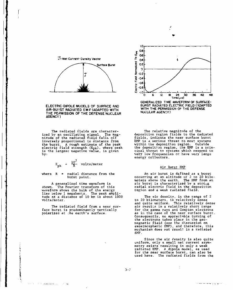
IN
I.0
Q8LU 0.6-
Net Current-Density Vector 9 0.4-
Surface Burst
Jo -0.2-
S-04-
Q-6.0.8
0 6 12 IS 24 30 36 42 48Time (Iss)
GENERALIZED TIME WAVEFORM OF SURFACE-ELECTRIC-DIPOLE MODELS OF SURFACE AND BURST RADIATED ELECTRIC FIELD (ADAPTEDAIR-BUPST RADIATED EM F (ADAPTED WITH WITH THE PERMISSION OF THE DEFENSETHE PERMISSION OF THE DEFENSE NUCLEAR NUCLEAR AGENCY)AGENCY)
The radiated fields are character- The relative magnitude of theized by an oscillating signal. The mag- deposition region fields to the radiatednitude of the radiated field falls off fields, indicate the near surface burstinversely proportional to distance from EMP is a serious threat to most systemsthe burst. A rough estimate of the peak within the deposition region. Outsideelectric field strength (Epk), where peak the deposition region, the EMP is a prin-is the largest negative value, is given cipal threat to systems which respond toby: very low frequencies or have very large
energy collectors.107
Ek = 7 volts/meterp IAir Burst iMP
where R = radial distance from the An air burst is defined as a burstburst point, occurring at an altitude of 2 to 20 kilo-
meters above the earth. The EMP from anA generalized time waveform is air burst is characterized by a strcig
shown. The Fourier transform of this radial electric field in the depositionwaveform shows the bulk of the energy region and a weak radiated field.lies below 1 megahertz. The peak ampli-tude at a distance of 10 km is about 1000 The air density, in the range of 2volts/meter. to 20 kilometers, is relatively dense
and quite uniform. This relatively denseThe radiated field from a near sur- air resulks in a relatively short range
face burst is predominantly vertically for the gamma rays and Compton electronspolarized at ;.-he earth's surface. as ini the case of the near surface burst.
Consequently, no appreciable turning ofthe electrons takes place in the geo-magnetic field (see the discussion onexoatmcspheric EMP), and therefore, thismechanism does not result in a radiatedEMP.
Since the air density is also quiteuniform, only a small net current asym-metry exists resulting in only a weakradiated EMP. A dipole model, as usedfor the near surface burst, can also beused here. The radiated fields from the
|.: 3- 7

air burst are similar in shape to thoseof the near surface burst, with the peakfields at least one order of magnitudeless then those of the near surface burst.
700
Due to the weak radiated fields, the j 60ZMP from an air burst is a principlethreat to systems which may be within thedeposition region, in which case, the
e c40other nuclear weapons effects must alsobe considered.20
Rh10
Exoatmospheric Burst EMP • ,0 . -. -6 I00 lo 0
An exoatmospheric burst is defined ___e__bo donshyP-as one which takes place at an altitudegreater than 40 kilometers above theearth. A typical exoatmospheric burstgeometry is depicted in the figure.
The Compton electrons are scatteredforward (downward in this case), withinthe deposition region as was the case forboth the near surface and air bursts.These Compton electrons produce a systemof radial currents. As stated previously,
EWPFROM G•,ALTITUiBUiRSTS a symmetrical system of radial currentswill not produce a radiated field. In
UXMPLE OFGEOI•NRYS CONSMWAD an exoatmospheric burst situation, thereare two mechanisms which produce the radi-ated field: (1) the asymmetry due to
burs__i_ - olse of Pooids the space/atmosphere interface, and (2)Compton electron turning due to the earth's
s gPuON sbiahglayer geomagnetic field, It is the Compton7" •-j-• "electron turning which dominates since the0km•k- •electrons can travel greater distances,
and thus have more time to interact withthe geomagnetic field due to the reducedatmospheric density.
k = height of burst •= 400 kmhs = distance to horzot - 2,250 km The outgoing gammas from the burst
form a spherical shell which expands withthe velocity of light. Since most of the
A high shitude burst illumuletes lrge geographlcal gammas are emitted in about 10 nanoseconds,regions with semas feys the thickness of the shell at any instant
is a few meters. When the gamma shellbegins to intersect the absorbing layerof the atmosphere, the Compton scatteringprocess begins.
9 £At the altitude of the depositionregion, the stopping range of Compton re-coil electrons is of the order of 100meters. In traveling this distance, theCompton electrons are strongly deflected
Above about 40 kilometers altitude, by the geomagnetic fiel.d with a gyro radi-the atmospheric density is sufficiently us of about 103 meters. The Compton re-small that the high energy ganmas are not coil current therefore has strong componentsaffe.ted appreciably. The atmospheric in direction6 transverse to the gamma prop-density is large enough that the gammas agation direction. This transverse currentare absorbed b. Compton scattering below radiates an electromagnetic wave that pro-40 kilometers. The gamma absorption is pagates in the forward direction.nearly complete by the time they reach20 kilometers altitude. The deposition re- The outgoing wave keeps up with thegion for a high altitude burst is thus be- gamma shell and is continually augmentedtween about 20 to 40 kilometers, which is by the transverse Compton current untilapproximately 65,000 to 130,000 feet. the gammas are all absorbed. Then the
3-8

electromagnetic wave goes on alone as a Compton electrons thet move parallelfree wave or pulse. Secondaty electrons to the geomagnetic field are not deflected.produced by the Comptons make the air Thus, the EMP amplitude is small in twoconducting. This conductivity attenuates directions along the geomagnetic fieldthe electromagnetic pulse. The amplitude line passing through the burst point. Theof E1'P is determined by a balance between: EMP amplitude is a maximum on those rays
from the burst point which run perpendicu-1. Increase due to transverse lar to the geomagnetic field in the depo-
Compton .urrent. sition region.
2. Attenuation due to conduc-tivity.
pi 7
MICHANISM Of EMP GENERATIN 'a CnO, IP ,
"Moemn rqyNý,I Compton e eectrom defleotsd
by $*majesflc fId.
Cumpton sett.erlg svet-The transverse current components
ano the resulting radiated fields can beunderstood by considering a system ofelemental dipoles along the line-of-sightfrom the observation point to the burstpoint. Each dipole radiates an electro-magnetic field (the normal "donut" radi-ation pattern of a dipole) which add inphase since the EM fields, gammas, and
A summary of the process of EMP gen- Compton electrons all travel at or neareration from a high altitude burst can the speed of light.now be given along with important detailson the directional dependence.
Gamma rays are scattered from mole-cules with the emission of Compton elec-trons in the forward direction with Burstenergies on the order of 1/2 million elec-tron volts. The motion of the Compton -EiTlhetOaelectrons is modified by the geomagnetic Oip,•,,
field. They follow a spiral path aboutthe magnetic field lines until they arestopped by collision with atmosphericmolecules. As the Compton electrons col- Observer
lide with atmospheric molecules, furtherionization occurs and the conductivityincreases. The propagation of the EMPdepends on the conductivity of the region =dd with the
through which it passes. Dispersion, o,,MAir o,attenuation, and reflection may occur.The circular component of the C(Xiptonelectrons represents a magnetic polariza- PHASED MAGNETIC DIPOLE ARRAY MODELtion, and the linear componet representsan electric polarization.
Both the magnetic and el.ectric pol-arizations vary with time and, conse-quently, can radiate electromagneticenergy. This can also be viewel as acollective flow of electrons alotg thefield which radiates in the transversaldirecti.on.
3-9
a

The radiated fields are high inten-sity fields, have short rise times (wide HORIZONTAL VARIATIONOF EMPspectrum) and cover a large area of the FROM A HIGH ALTITUDE BURST
earth's surface because of the height andlarge extent of the deposition region.The geographical coverage as a function N-1-.0
of the height of burst can be obtained by Burs
considering the tangent radius.
The tangent radius is the arc lengthbetween the line from the earth's centerto the burst point and the line from theO -earth's center to the point where a line .from the burst point is tangent to the Z.r. '
surface of the earth. For a burst at 300kilometers, the tangent radius is 1920 ,4,d _j
kilometers, or about 1200 miles. TheEMP from the burst can cover this region.
It should be noted that the fields At surface zero, the fields have re-do not end at the tangent radius. For duced amplitude (0.25 Emax), short risesurface systems, this is the farthest time (approximately 5 nanoseconds), andpoint of interest, in most cases, but low time to half value of about 20 nanoseconds.amplitude fields may be propagated beyond At the maximum field location, the risethis point by ducting. For airborne sys- tixie is about 10 nanoseconds and time totems, however, the coverage may be much half value is about 50 nanoseconds. Atfarther depending on the height of the the tangent radius, the fields are aboutpoint of observation. As long as there 0.5 Emax, and rise time to half valueis line-of-sight to the burst point, the greater than 10 nanosecornds and 200 nano-EMP will be present. seconds respectively. This distribution,
as a function of height of burst and geo-graphic position on the earth, can bedetermined from the figure, The peak
TANGENT RADIUS FOR A field at any point can be found by align-HIGH ALTITUDE BURST ing magnetic north on the figure with
magnetic north at surface zero.
h26000
2400 Tangent Radius
2200o O5Emx
-2000-
* 1800
1400 - )5Emo- W.25Eumx North
1200
1000 - Null Area
0 t 2 0 0 -0 Surface Zero100 200 300 ;oo .ooh (k1m)
2xH08Region OfH-- Maximum Peak
Electric Field
The EMP time waveform varies consid- Radius,R"erably over the area of coverage. Three Rd "cases will be considered: (1) near sur-face zero, (2) the maximum field point 0.5EM8 1
(where a line from the burst point to the VARIATIONS IN HIGH ALTITUDE EMP PEAKmaximum field point is orthogonal to the ELECTRIC FIELD ON SURFACE OF CONT-geomagnetic field lines in the deposition INETAL UNITED STATES (ADAPTED WITHregion), and (3) at the tangent radius THE PERMISSION OF THE DEFENSE
, point.pitNUCLEAR AGENCY)
3-10

As a result of this wide variationon the earth's surface and the inabilityto predict the burst location, the timewaveform used preserves the importantcharacteristics of the three waveformsdiscussed. The composite waveform, there-surface zero rise time), slow decay (near so-
tangent radius decay), and maximum eak -amplitude. The spectrum contains X Rfrequencies of interest. The compositewaveform, shown in the figure, can be 60 / Spectrum jcpproximated analytically by a double /
expnenial 1 80 /'Normalized CumulativeE(t) = 5.25 x 10⁴ [e"•t e 8 t] 40 / Energy-Density Spectrum
where 30 / - se I1a 4x10⁶
20 : 107hhl~pL~S = 4 1 6. . .. . . . ' ' '... ... ' " • ,
2% 105 104 10? 106
= 4.76 x 1O8 Frequency(H)HIGH-ALTITUDE EMP SPECTRUM AND NORMAL-IZED ENERGY DENSITY SPECTRUM
50 -- _The polarization of the EMP dependson the locations of both the burst and120 the observer, and the orientation of the
40 -1geomn:gnetic field. The direction of the> electric field is normal to both the geo-
-• magnetic field at the observer's location,so t and the direction of incidence. The dir-
"ection of incidence is radially outwardfrom the burst. For the Continental U.S.,
Szo a typical dip angle for the geomagneticfield is about 67 degrees.40 A40
For this dip angle, and assuming the-202 geomagnetic field lines run north and
south, the EMP polarization is horizontal__......_____ _ for bursts north or south of the observer.
1O-10 t0-, to-$ to-, 1o-6 For bursts east or west of the observer,Time W) the polarization departs from horizontalby 23 degrees or less. Therefore, theGENERALIZED HIGH-ALTITUDE EMP ELECTRIC- principle polarization for systems basedAND-MAGNETIC-FIELD TIME WAVEFORM in the U,S, is horizontal.
3.4 EARTH EFFECTS ON TOTAL FIELDS
So far we have discussed the freefield which impinges on the surface of theearth due to the radiated EMP. Since theseare electromagnetic waves, they will pene-trate the surface of the earth and be re-flected by it. The amount of penetration
The spectrum of tihs pulse can be or reflection is a function of the fre-obtained by taking the Fourier transform quency (spectrum of the pulse), the polar-of the time waveform. The significant ization, direction of incidence, and earth[ frequencies extend out to about 150 mega- parameters.hertz with the bulk of the energy (99.9%)below about 100 megahertz.
3-11

The reflection and transmission co-efficient equations are presented inSection V. It should be noted that a s Vc mr i "•°"phase reversal takes place for the compo- s.,,.i, Lnent of the electric field parallel to5 ,, 6""" , 5the conducting surface but not fox the Stk,, ing
normal to the surface component. Near -sU,the surface, therefore, for the parallel acomponent, the electric field is reduced, 401..,J
but the magnetic field is increased.Electromagnetic fields alsoi diffuse into e
the ground. The penetration depth de- 1; ,• 7n , 7pends on ground conductivity and frequency
component considered, A greater ground External EMP Internal £MPconductivity leads to a smaller penetra-tion depth, The high-frequency componentspenetrate less deeply than the low-fre-quency components of the pulse.
Internal EMP can arise in differenteleoWk field strength ways. One type may be called "cavity
EMP" and arises from Compton recoil elec-moist ground c - 102 mhosr trons being driven across the volume of
depth an enclosed cavity. Both electric andvery drygrovd o- 10-4 mhos/m magnetic fields are generated. These
fields may ring at the cavity frequencies.The fields will induce voltages in cir-
f 10 MHz cuits contained in the cavity. If thecavity contains air, it may become elec-trically conducting. This affects thetime behavior of the fields.
"letik filod strngt
10il 2 mhos/
depth -410 mhes/n E,,e , V,,d
Magnetic Field SMIlaI go.
f = 00 ~zur /
3.5 SYSTEM GENERATED AND INTERNAL EMP Coanipln ElectionSpace Chargve
While not the subject of this course, Cavity EMPa few words are in order in the area ofsystem generated EMP (SGEMP) and internalEMP (IEMP).
Internal EMP is EMP induced directlyin a system by gamma radiation (or X-rays)striking the system. In the case of in- Another internal effect (SGEMP) isternal EMP, Compton recoil electrons are "Compton charging." Any object in a gammaproduced by interaction of incident gamma flux has some Compton electrons knockedradiation with material in the system. out of it and receives Compton electronsThis interaction is similar to production knocked out of other nearby objects. Theseof Compton recoil electrons in the atmos- will usually not balance. The charge addedphere in the case of external EMP. How- at various locations in a conducting cir-ever, the way in which Compton recoil cuit will flow away through the circuit,electrons produce internal EMP differs thus generating an extraneous signal. Thefrom that of the Compton recoil electrons charge acquired by insulation may leakin external EMP. away very slowly. In general, the thicker
the object, the more charge it acquires.
3-12

We will not discuss further cavityEMP or Compton charging in this course.This does not mean that they are unimport-ant, but rather that they are anotherproblem area sufficiently different fromEMP to be considered in a separate course.
Wire
Icidento oy- Flux Recoi! Eiectrons
Entering Compton RecoilElectrons From Nearby Objects
Compton Charging
This very brief discussion doespoint out that IEMP and SGEMP are ofprimary concern to space systems or tosystems which are within the depositionregion of the burst. These effects bothrequire direct exposure to the incidentgamma flux which occurs only in the de-position region for near surface or airbursts. Since the gamma rays are notabsorbed in space, space systems evenat considerable distance may be exposedto the gamma flux.
3-13

SECTION IV
EMP INTERACTION AND OOUPLENG ANALYSIS
4.1 INTRODUCTION
To be able to assess the effects of For a sinusoidally time varying fieldEMP on a system, the way EMP interacts to be plane, the electric and magneticwith the system and thn extent of this fields must be mutually orthogonal and ininteraction must be understood. The dis- phase everywhere in a plane perpendicularcussion cn interaction will consider, in to the direction of propagation. In addi-a qualitative manner, the important as- tion, if the magnitude of the electricpects of electromagneti: coupling. The and magnetic fields are independent ofdiscussion of coupling analysis v'iil re- position in the plane (i.e., the magnitudeview methods fo- obtaining quantitative of the electric field and magnecic fieldestimates of this coupling, at any instant of time is the same any-
where in the plane), the wave is definedIn discussing interaction, we will as a uniform plane wave.
consider the principles by which energyis transferred from the electromagneticfield to collectors. The effects of theearth and other structures which may al-ter the incident electromagnetic fieldwill be considered. The mechanisms bywhich shields and cables work and bywhich electromagnetic energy may pene- Propagation of a Uniform Plan. Wavetrate into the system interior will alsobe discussed.
The discussion on coupling analysiswill consider the basic methodology for Epredicting, in a quancitative way, the P-" -,ExHenergy transferred by an electromagnetic .7_- -Zfield to a collector. Examples of the Di'actjon of Przpauationapplication of this methodology to such Atittocollectors as antennas, cables, and con-ducting structures will be discussed. "Equi-4has Plane
4.2 EMP INTERACTION WITH SYSTEMS
The interaction between an electro-magnetic wave, such as EMP, is highly de-pendent on the characteristics of thewave, the characteristics of the system,the characteristics of the propagatingmedia, anid the media or structures in thevicinity of the system of interest. The The wavelength, X, of a monochromaticrole each of these plays will be discussed (single frequency sinusoidal) plane wavein this section. is the separation distance between planes
in which the E vector in one plane is inThe Plane Wave time phase with, the E vector in the refer-
ence plane.Outside of the deposition region for
a near surface nuclear burst, the propa- The uniform plane w.:ave has other prop-gating EM wave can be modeled as a plane erties that make it convenient to workwave, For the exoatmospheric burst, on with. One of these is if the wave isthe surface of the earth, the EMP can propagating through a nondispersive (loss-also be locally modeled as a plane wave. less) mEdium, the electric and magneticModeling the EMP radiated wave as a piane fields are related through the spatialwave, or a uniform plane wave, implies impedance of the medium, called the in-very well defined characteristics. trinsic impedance of the medium (11).
AL -I

When a uniform plane wave is a pulsedfield in the time domain, such as the EM?from a nuclear detonation, it may be con-sidered as consisting of many frequenry
n. components constituting the frequency, i1 pactr of the fields. In this case, theSnd rfoeflds are functions of the radian
frequency (w). The power demnsity of an " // 377 fn in air or free uniform plane wave for the pulsed field is
space defined as a spectral power density and isThe velocity of propagation of a plane given by:wave through a nondispersive medium isthe velocity of light through that medi- E 2 2um. If C is the velocity of light, P - - watts/m Hzthen
S18 A perfectly uniform plane wav• cannotC x 10 meters/sec in exist in nature; however, it is an extreme-
/P_ air of free ly useful and reasonably accurate approx-space imation for such wave fronts as spherical
and cylindrical waves which are comron innature, providing the proper conditions
If the plane wave is monochromatic, the are met. For example, the free-space,ýhase shift per unit length due to the far-zone field of a radiating monopole an-inite propagation velocity is given by tenna is a spherical wave.
the phase constant, 0.
L 2IT •- •/- radiaiis/meter
w- 2rf radian freq, ency. "p= \ \The average power density of a uniformplane wave (single frequency CW) is Iq•given by the magnitude of the Poynting Radiating _ -vector •. •0 •
l~ - x Al iijisin 6 watts/mn l77 /////j 7
8 = angle between 9 and A
If tm and Am are the maximum values ofthe sinusoidal fields of a uniform jianewave, then the average value of the powerdensity is given by To a distant receiving monopole antenna,
a 'the wave appears as if it were a uniformLM Im 1tm Iplane wave since the receiving antennaav-- = 2 is sampling only a small portion of the
/ /7 2 spherical wave 5ror~t. This same criter-ion must hold for the case of the EMPwave front; however, it is difficult to
2lml2 define the 'Ir fields from an EMP sourcewatts/m2 region in te•.-mv of equivalent antenna
dimensions of the source. in the caseof a near-szfpace burst, the dipole modelof the source region can be consideredas a point sourcVM so fields outside thesource regivn ca\'wbe considered planareven for systems -v few kilometers long.In the exoatmospheric case, the sourceregion is widely distributed. The fieldson the surface of the earth are the re-sult of an elemental dipole array model,the time of arriLval difference, even forsystems many kilometers in length, is sosmall that the wav• can be approximatedby a plane wn'e.
4-2
III

..g'4elds Due to EMP This waveform, as presenteO, has adc component which cannot exist in a radi-ating wave. Unless this is recognized,
The preceeding paragraphs discussed some non-physical results can be obtainedthe wave nature of the EMP and the rela- in coupling analyses. The portion of thetionahip beckwan the electric and magnetic spectrum below the audio range (10 kHz)fields. To understand the interaction of is presently being investigated.the EMP with systems, the time and fre-quency distribution of the pulse must be Many EMP collectors (antennas, aerialreviewed, and buried cables, structures, etc.) are
particularly frequency selective. It is,Consider the electric field time threfore, desirable to determine the EMP
history for a test waveform which approx- frequency spectrum by taking the Fourierimates a typical high altitude EMP in free transform of time waveform. The plot ofspace. The waveform exhibits an extreme- the magnitude of a nominal EMP spectrumly fast rise time (_ 5 ns to 10 ns be- indicates twc break points associated withtween the 0.1 and 0.9 Emax amplitudes), and the fall and rise time of the time wave-a slow decay (.G 500 ns to I ps, 0.9 to form. It is important to note that the0.1 Emax). For analytical purposes, the spectrum is almost constant below the HFwaveform usually can be approximated by a range. Between the first and second break-supcrposition of two exponential functions frequency, the spectrum falls off at 20as dB/decade. Above the second break-fre-
que,icy, it falls off at 40 dB/decade. Al-t e t vso shown is the cumulative energy density
E(t) - A WO e volts/m which is normalized to 0.9 joules persquare meter. Approximately all the EMP
Assuming the wave to be a plane wave in energy (> 99 percent) is concentrated be-frep space, the magnetic field has the low 100 Mlz.same time dependence (shape) and is re-lated to the electric field by
HIt) L) amp/m"nro
where
= 377 ohms (intrinsic impedance so-of free space) Vo /
5 1/Normagild CumtlotIvg50 Energy en•ity pttufru r
00 , 9 106 1O 07 *o6 1030 so FrO* 1Cy 1om1
HIGH-ALTITUDE EMP SOECTRUM AND NORMAL-
•o 20 60 IZED ENERGY DENSITY SPECTRUM
U 0rt 40
to
i0-N 0-9 I0-41 o0- g0-6Time (9)
GENERALIZED HIGH-ALTITUDE EMP ELECTRIC- The pulse shape given here is for aAND-MAGNETIC- FIELD TIME WAVEFORM nominal EMP. The pulse shape to be used
for a particular scenario for a systemanalysis should be obtained from the De-fence Nuclear Agency or the service leadlaboratories.
4-3

The two factors of the EMP that con-tribute to the threat to electrical andelectronic equipment are: (1) the largeamplitude of the fields, and (2) thebroad spectrum. EMP energy collection ofa given system is a function of the systemresponse to all frequencios in the EMPspectrum. The system transfer functionmay exhibit responses to both in-band andout-of-band frequency "windows". Out-of-band energy collection is ý result of the" ystem having a frequency response greaterthan needed to perform the system's func-tion. This added frequency response canbe deliberate (the designer wanting tohave a better response than actually re-quired), or can be non-deliberate such asspurious responses in a receiver. Themain concern ir. the case of EMP is due tothe broad spectrum; it is imperative inassessing the system vulnerability thatthe overall system response be determinedand utilized in any analysis effort,
A structure can collect energy froman impinging EMP fielG by electric in-duction. In effect, charges on a conduct-ing surface are separated by the tangen-tial component of the impinging electricfield which results in current flow. Theoverall result is that a voltage source
T(jw) distribution is induced on the conductor
Slystm consisting of incremental (point) voltageam Trpnfer generators. The contribution of each
uCv-n point generator to the current at somepoint on the conductor is determined byits transfer admittance, which is a func-tion of the source and observation points.IT wI iwk A
Nespone. of a *ystemn to IMP
Electric inductionCopper Wire
ElM Induction Principles C Ihrge Separation
There are three basic mechanisms bywhich the EMP energy couples to a con- _ducting structure. These are: (1) elec.-tric induction which is the principlemechanism for linear conductors, (2) mag- • *EAZ
netic induction which is the principlemechanism wh i- Lhe condu.cting structure Equivalent Point Source
forms P ziosed loop, and (3) through the
earti transfer impedance which is theprinciple meechanism for buried conductors.
4-4

A coupling structure can also collectenergy from an impinging EMP field by mag-netic induction. The induced signal froman EMP is equal to the negative time rate AV ZTJ Azof change of the incident magnetic flux.This is an empirically derived fundamentallaw known as Faraday's Indaction Principle. whereThe voltage induced in a loop by a uni-form magnetic field is given by J = total earth conduction current
per meter widthv (t) H(t) ZT = surface transfer impedance of
the earth.
where
= 47 x 10-7 is the permeabil- The surface transfer impedance is givenity of free space by
A = the area of the loop ~T 6 /~~
H = The component of the mag- wherenetic field normal to theplane of the loop. = propagation constant of the
earth
= free-space propagation con-stant
6 = earth conductivityMagnetic Induction
d = depth of burial.Loop Antenna
00 •H + * Transmission line theory may now be_4 used to determine the actual current dis-
HEI e tribution induced on the wire.
Equivaier-. CircuitArea - A.
Current Flow due to I-Z Drop in the Cround
Another important coupling mechan-ism is that due to the I-Z drop which Er Poccurs whenever a coupling structure isimbedded in a lossy medium, e.g., earth, H,in which EM fields exist. Consider, for H<example, a bare wire conductor located a Grounddistance, d, below the surface of theearth and in the presence of an impinging /77777- 77+777' ZEMP field as shown. The incident EMP ?no,field illuminating the surface of the dnea•'th causes conduction currents per meter -width to flow in the earth. As a result +-AV- I AVZZTJAZof the current flow in the earth, a dis- .-- Itributed I-Z drop appears along the wirewhich is equivalent to a voltage sourcedistribution, causing current to flow inthe wire conductor. An increment ofvoltage drop (which can be viewed as apoint generator), AV, over a distance.Az, along the conductor is given by
4-5
,p

Antennas T Dmax/c -- the time it takesan EM wave to travel thedistance Dmi at the velo-
Electromagnetic coupling to antennas city of ligh t c.results from electric and magnetic in-duction. The induction principle which Then a coupling structure is electricallydominates fog a given antenna depends on small ifthe antenna's geomietrical configuration.At this time we will ccy'sider two basic, Xisimple types: (1) thelinear antenna Dmi(monopoles or dipoles•, and (2) the loop max -antenna. The way energy couples to thesesimple antennas can serve a-y a basis forestimating the ene gy collt ction by com- (Frequency-domain criterion)plex antennas and .. a oth¶c conducting orstructures.
S* tr > 4T
Linear Antennas
When an electromagnetic ,Yarý inv- (Time domain criterion)pinges on a linear antenna, the tan.,&.ntialcomponent of the electric field inducescharges on the antenna which tend to c•a- wherecel the incident field. Since thesecharges are free to move, an antenna cut- fc = 0"61trrent results. In a time varying field,therefore, these charges are constantlyin motion and an alternating current flows t = rise time of EMP excitation.on the antenna and in the load. r
Electric induction on a linear an-tenna can be viewed as an array of pointvoltage sources. To obtain the totalvoltage induced on the antenna, all of the.point sources must be summed (integrated)over the length of the antenna. If theantenna is short (antenna length < 116the wavelength of the incident signal), it Dipole
is not necessary to .Derform the integra- -*t
tion. In the case o7 EMP, since it is a -- .transient signal containing a wide fre- Does_ .
quency spectrum, the antenna length mustbe < 1/6 the wave'ength of the highest T.,, O
frequency component of interest in the Loop -
spectrum. For typical EMP waveforms, theactual physical length must be less than 4(0approximately two (2) feet. N ,LEO _ fc,.O.6/,,
Considerable simplification results ' .when the &1P coupling structure is elec-trically small, since, for such structures, Electrliclly-Small EMP-Coupling Otru~tures
simple equivalent circuit representationsare possible. It is essential, therefore, Ito establish appropriate criteria or thebasis of which it would be possible todetermine whether or not a particularcoupling structure, i.e., an antenna, iselectrically small.
Definitions Loop Aotennas
D = maximum dimensions of Loop type antennas can couple to ancoupling structure measured electromagnetic wave Through either thefrom its load terminals to electric field or the magnetic field. Athe most distant point on - litage will be inducid in a loop antennathe structure, if a time-varying eý.ectric field has a
component parallel to one of the sidesf= maximum significant frequency of the loop, or a time-varying magnetic
component of the EUP spectrum field component normal to the plane of
4-6

the loop. As stated earlier, a time The magnetic induction (H), resultsvarying magnetic field induces a current from the flux change between the cablein a loop antenna such that the magnetic and earth. This induced voltage appearsfield produced by the current opposes the as an incremental series voltage source.applied field. The electric induction (E), results from
the displacement current which flows be-As ir, the case of linear antennas, a tween the cable and the earth due to the
very simple relationship between the field stzay capacitance. It appears an an in-and the induced voltage exists when the cremental shunt current source. The volt-loop it electrically small, or stated age source associated with the intermediateanother way, tle field is uniform through- conversion impedance (Z C), results fromout: t", area of the loop. For a loop to the current flow in the earth due to itsbe c&Isidered small, its diameter must finite conductivity. This source appearsblý 1 thliX ýh /6. For typical EMP as an additional incremental voltagewVvEO rr. S! h~i esults in a physical di- source in series with the load. All ofa~eteV .fss than 2 feet for a loop in these incremental contributions must befree spa summed in the proper time-phase which takes
into account the earth parameters and theangle-of-arrival.
CablesFor long runs of cable which run
Cabling may be considered in two over or within the ground, ground para-broad categories: (1) unshielded, and meters as a function of frequency are im-(2) shielded. In the case of unshielded portant. Also important for the pickupcables, they may be considered as E and for these long runs is the angle-of-arri-B collectors as previously discussed for val and both the low frequency and thelinear or loop antennas. Coupling to high frequency content of the EMP wave-unshielded cables can also occur through form.an intermediary conversion impedance (Zcd If the cables are buried within the
ground, the principal pickup mechanism tocause current to flow on the cables is thecommon impedance mechanism. Electric and
Unaield&d Cables mey be Considered ns: magnetic fields cause currents to flow inthe earth, and the resistance of the earth
Sipo.S ls Loops causes a voltage drop to appear along the
4$.> C ollector °Coll.cto,. c
or
Tied in ,ith hie hltormedisltConversor lmp,:dsrc a ZC
H
For a cable above, but in proximity• to the earth, all three interaction mech- -
anisms are present. The height of thecable above the earth, the etrth para- Azmeters, and the parameters of the EMP alll _
impact the energy coupled.+ A
Cable Abcve GroundBURIED CABLE
ý l V. 1z'7i 1-7
4-7

For shielded cables, the shield is Magnetic field penetration resultsviewed as a cylindrical shield. The wires from aperture coupling and diffusioninside the shield interact with the pene- through the shield, especially for thin,t ating fields through the same mechanisms nonferrous shields. The penetration mech-(I and f) as the unshielded cables. The anisms for shields is discussed more fullypenetrating fields, however, are altered in the shielding section.y the shield to reduce the field ampli-
tude and change the spectral content. A In the case of coaxial cables, theform of intermediate conversion impedance interior magnetic field pickup can occuralso plays a role. In the case of shielded because of the asymmetry, A, between thecables, it is called the surface transfer idealized position for the center con-impedance (Zt-) and is a characteristic of ductor and the actual position of thethe cable shield, center conductor as it occurs in the manu-
factured cable. This asymmetry essential-ly results in loops of unequal area andtherefore unequal voltage being induced.
Shield Penetration Mechanisms
Electric Through Holes Magnetic Field Penetration
Asymmetry Pickup
Magnetic • Through Walls ando4 . -_ _ - ..... __7____-
Holes -
T
Sheath Current: I ZT Drop TAlong Cables The primary pickup mechanism for
shielded open wire pair cables is alsothrough the B mechanism. The loop in thisinstance is closed by the terminations atboth ends of the cable.
Electric field penetration general-ly occurs through the apertures or smalldefects in the exterior shield of thecable. Electric field penetration is al-so associated with connectors which are Magret-c Field Penetrationnot fully shielded. In addition, theelectric field is often enhanced at theterminations of long exposed cable runs,and this contributes greatly to electric Open Wire Pair & Pckkupfield penetiation effects.
Electric Field Penetration 41.
H Braid Shiell.
Here we see the definition of theintermediary conversion impedance,'betweenthe external fields and the inside voltageof a particular cable. The surface trans-fer impedance is defined as the voltageappearing on the inside of tne cable ona per meter basis due to the current flow-
Aperture Penetration 'ng orx the outside sheath.Through Simple Holeor Holes in Braid
4-8
'

tion effect and, therefore, has an improv-ing transfer impedance with frequency
Sheath Current Pickup primarily because of skin-effect absorption.
Surface Tr.nsfer Impodance of Braided and
7 7 1 11//1711/1/ I I T / /I//Solid Outer Condictor Coaxi., Cable
N
einsideZT s Bsheath _ 10 raided
10U Z
*t 0.1_S * i I l |o,0.I 1 10 00O
The surface transfer impedance plays Frequency IMHz)
a very important role in evaluating thecable performance. Transfer impedance isimportant for electric field pickup be-cause the E field can induce currents toflow on cable runs which are parallel tothe electric field as illustrated by the There are some favored approaches re-cable which terminates in a UHF antenna garding cables. One favored approach ismast. Sheath current also flows or. in- the use of twisted wire cable to minimizeadvertent loops formed by cable runs and the A pickup. This twisted wire cable isother metallic structures. also shielded to minimize the E pickup
effects. However, the E-field pickups dooccur with the presence of sheath currents.The sheath-current-Induced inside voltages(common mode pickup) are mi.nimized by theuse of balanced terminations which, ineffect, are not connected to the externalsheath.
Role of Surface Tranz-fer Impedance
3 .2 Minimization of Pickup
Cable asPseudo Antenna Ca1l" as QUa&l-Loca
S--V -I-1
(I) Twisted-Pair Minimiaen H Pickup
The trensfer imr,edance is ve-y im- (2) Balanced Termination mirimimela
portant and at low frequencies is about Sheath Cu rent PIckup
the same for both braided and solid wallouter shields of the same coppex content.However, in the case of the braid, bc-cause of the field penervatiuns through L_apertures, the Lransfe-: impedance increaseswith frequency, thereby dramatically in-creasing the pickup characteristics ofbraided cable. On the cther hand. solidwll cable does not exhiLbit this penetra-
4-9

The terminacions and splices alsocan play a major role in enhancing thecoupling effects associated with long ca-ble runs. In the case of a balanced pairwithin a cylindrical shield, the cable Summery for Cable Pickupshould be Lerminated both for the balanceand common mode terminations. Small im-perfections along the surface of the cable * Mechanlumaera E, B. ndZcan convert some of the common mode pick- * Shielding by outer conductor mustup into differential mode pickup and vice be consideredversa. Thus, if the cables are not proper-ly terminated for both modes, the pickup 0 Time delay effects become important
and reverberation effects are greatly en- * Terminations can contribute to the pickuphanced.
ftlanced Pair Termination
____................. _Shielding and Penetration
zsaienc!d As discussed previously, propagatingz Common- EM waves have coupled electric and mag-mode netic fields. In general, whenever you
have a time-varying electric field, thereis an associated time-varying magnetic_field. At low frequencies, however, this-oupling is relatively loose and electricSnd magnetic field penetration effects can
In the case of multi-conductor te considered separately on a practicalbundled he allssoe of u-ndsorae basis. This separability of the fields
bundled c.4blee, all sorts of undesirable permits defining the figure of merit (shield-effects co n be produced by cross-talk em- ing effectiveness) of a shield separatelyfects on the terminations. for the magnetic and.electric field pene-
tration. The inside fields are generallythe fields in the geometric center of theenclosure. The outside fields are thosefields which would appear at the samespatial point as the inside fields with
Multi-Conductor, Bundled Coble Termination the enclosure removed.
.. .Shielding Effectiver.ess at Low Frequencies
(SE) . 20 log (Hinside)E inside
In summary, cable pickup mechanisms (sE)t 201log(Enside)are an extension of E, H and Z coupling.The same holds for shielded cables except"the effect of the shield must be consid-ered. Improper terminations also play amajor role in the pickup associated withcable runs. In the case of very longcable runs, time-delay effects become im-portant and give added weight to angle-of-arrival, earth parameters, and thelower or higher frequency content of theEMP waveform.
4-10

At the higher frequencies, the elec- vaiue is obtained. In generai, thesetric and magnetic fields must be consid- measures are each self-consistent withered jointly. In many instances, the frequency but can have values which dif-power flow is a convenient form of defini- fez by as much as 20 or 30 dB. The dif-tion. In this case, the power flow, in ference between these two measurements isthe absence of the enclosure, is comparel the small loop technique only measuresto the power flow with the enclosure pre- the shielding effectiveness in a localsent. This is somewhat of an unwieldly area. The plane wave technique, on thedefinition and a more appropriate defini- other hand, provides for current flownition might compare the energy inside simultaneously on all surfaces and thusthe enclosure with the energy in the ab- edge and corner effects are seen. Thesence of the enclosure being taken as a small loop measurements are, therefore,stored energy over a specified volume useful to determine seam leakage, etc.,(the volume of the enclosure), and the plane wave for overall structure
shielding effectiveness.
In EMP, we are dealing largely withplane waves w.lhere the transient responseof the enclosure l.q important. Thus, the
Shielding Effectiveness at High Frequencies amplitude response, as a function of fre-quency, must be related to the transientresponse. There are some rather simple
iSEVO 10g P i.ways of doing this which will be consid-' outside ered in more detail. However, before do-
ing this, let us consider on a qualitativebasis how shields actually work.
(SEI,- 10 log ( Winside )Woutside
The shielding effectiveness is gen-erally presented as a function of frequen- Shielding Ef'rctlve,.., as a Function of Measurement Methodcy. This is convenient for many radiofrequency engineering-type applicationsbut forms a major stumbling block in trans- CW Saw,. Field Strength Meterlating this rather simple concept into theappropriate EMP requirements.
SE Scoapoberconee ha h
Shielding Effectiveness Presented as aFunction of Frequency method.
W/
log w -0.
It must also be recognized that theshielding effectiveness often stated is astrong function of the measurement method.For examplL, if the shielding effective-
4 ness measurement is made with two smallloops adjacent to the wall, one value ofshielding effectiveness is obtained. If,on the other hand, the shielding enclosureis placed within an EMP simulator, another
4-11
A
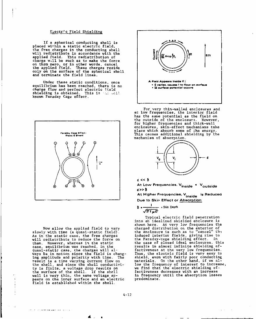
Electr'c Field Shielding
If a spherical conducting shell is " +
placed within a static electric field,the free charges in the conducting shellwill redistribute in accordance with the ef -~ E~t)
applied field. This redistribution of Pi
charge will be such as to make the forceon them zero, or in other words, cancelthe applied field. These charges resideonly on the surface of the spherical shell "---and terminate the field lines.
Under these static conditions, once A Field Appears Inside If:
equilibrium has been reached, there is no e I vries, causes c to flow on c urs aecharge flow and perfect electric field " surfcepotantialoccus
shielding is obtained. This i .!known Faraday Cage effect.
For very thin-walled enclosures andat low frequencies, the interior fieldhas the same potential as the field onthe outside of the enclosura. However,
for higher frequencies and thick-wallenclosures, skin-effect mechanisms takeplace which absorb some of the energy.
SardtiCae EfIt: This causes additional shielding by the
mechanism of absorption.
VO Vi
+ ~ ' > + At Low Frequencies, Vinside a Voutsided>>8At Higher Frequencies, V inside is Reduced
Due to Skit Effect or Absorption
I = Skin Depth
Typical electric field penetrationinto an idealized shielded enclosure isshown here. At very low frequencies the
Now allow the applied field to vary charged distribution on the exterior ofslowly with time (a quasi-static field). the enclosure is such as to "cancel" thb,As in the static case, the free charges induced interior fields, giving rise towill redistribute to reduce the force on the Faraday--cage shielding effect. Inthem. However, whereas in the static the case of closed ideal enclosures, thiscase, equilibrium was reached, in the results in almost infinite shielding ef-quasi-static case, the charges will al- fectiveness at the very low frequencies.ways be in motion since the field is chang- Thus, the electric field is very easy toing amplitude and polarity with time. The shield, even with fairly poor conductingresult is a time varying current flow on materials, On the other hand, if we al-the shell, and since the shell conductivi- low the frequency of interest to increase,ty is finite, a voltage drop results on we find that the electric shielding ef-the surface of the shell. If the shell fectiveness decreases with an increasewall is very thin, the same voltage ap- in frequency until the absorption lossespears on the inner surface and an electric predominate.field is established within the shell.
4-12

Magnetic Field ShieldingTypical Electric Field
(SE)E Idealized Shield As in the case of electric fieldshielding, to obtain magnetic fieldshielding it is necessary to establishan induced magnetic field (interior field)
6dB Octave which will cancel the applied field (ex-terior field). A magnetic field results,in the case of a conductive structure,from the current induced in it. The in-duced current results from the principle
W" \ of magnetic induction which requires aO- time varying applied magnetic field.0 ot
-N d<<8 d >>8 Consider a conducting loop in the> Reflection Reflection and presence of a time varying magnetic field.
Region Absorption Region The induced current, due to magnetic in-duction, establishes a magnetic field
Log Frequency -- which reinforces the applied magneticfield exterior to the loop, but opposes
Electric Field is Easy to Shield or cancels the field in the interior ofthe loop. If a number of loops were"stacked" to form in the limit, a conduct-
Now consider the relationship be- ing box or volume shield, the fields ontween pulsed fields and the shielding ef- the interior of the box are surpressedfectiveness as a function of frequency. at the expense of enhancing the fieldsThe pulsed field contains a wide spectral outside the box.distribution. The amplitude of the pene-trating field is a function of frequencyand so is the phase. For thin wall en-closures, the fields appearing in theinterior of the enclosure are roughly thetime derivative of the applied (exterior)field. On the other hand, for thick walledenclosures, the amplitude of the interiorfield is substantially reduced and thederivative effect tends to disappear.This is particularly noticeable in the Reinforcescase of ferrous metal shields due to in- Herecreased absorption.
H
H-9-T
Meah-BoxTh-, Aluminun Shell
( SE1E
LL/
Fe-i t SE11
hE TTh,
4-13

The current flow on a closed box, As the frequency continues to in-however, is not uniform. The current crease, the shielding effectiveness be-flows around th. box and near the edges. gins increasing at a higher rate. ThisThis occurs because adjacent eddy current is due to skin effect absorption as ir.elements cancel on the faces normal to the electric field case.the magnetic field.
Out-of -Phose bRe1gio-n
Log w
A. i A(]Ju)
zL RS+ Jv LLow Frequency : High Frequency:
Aljwrn) At
As noted, the shielding effective-n~ess, as exemplified by ordinary wallmaterials, such as thin-wall iron, thin-
.1/ wall sheet iron, coppeer or aluminum, ex-~ ~ .-. ~..~.hibit very poor low-frequency magneticshielding effectiveness. Where this is arequirement, the magnetic flux may beducted away from the area of interest bya ducting 'high-perm" shield. This re-quires , in general, a high product betweeathe relative permeability of the wall ma-terial and the ratio of the wall thicknessdivided by the average radius of che en-closure., In general, such approaches arenot practical with ordinary shieldingmaterials because of weight and cost.
Both the magnitude and phase of theDutn pretAinduced current on a conducting box are a catg iron, oeroau Shielding
function of the frequency of the appliedm'field. The magnetic reflection or cancel-lation effect occurs because the currentflowing in the outer ring becomes more------
end more in phase with the applied field.At the low frequencies, the current flow- ting in the outer ring, as seen in the e- en--- -
quamion, is almost 900 out-of-phase withcthe applied field. At higher frequencies,current in the outer ring becomes almostin phase with the applied field, and.,thereby provides better cancellation, whichincreases the shielding effectiveness atthe rate of 6 dB per octave. A necessarycondition is that the wavelength is muchlarger than the radius of the loop. necessary
4-14

We have discussed how the magnetic ducing a voltalge drop across the adamfield shielding effectiveness varies with which appears on the inside of the en-frequency, The relationship of this vart- closure which i3 very important if multi-ation with frequency to a transient re- point grounds are utlized.sponse must now be considered. Thesecurves show a typical transient waveform __.. .....applied to an idealized shield (no aper-tures or penetrations). Note that thepenetrating magnetic field waveform is Ofect of Seemns Without Apelur1stretched out by the shield and that alarge volume shield exhibits greater mag-netic shielding effectiveness than a smallvolume shield. In the case of ferrousshields, the penetrating wayvforms arefurther reduced due to the higher pdrmea-bility. The most important feature of theferrous shield is the stretching out of Low-Reoeieenothe rise time of the interior field, re- (SE)H seam gHih-Reelatenoesulting in smaller coupling to interior Seemconductors due to magnetic induction (BA)effects. The interior fields are roughlythe time integral of the exterior magneticfield and decay exponentially. w--
Tvpm.l Mognetic FWtd Sk,1 g * tg If 1es
,d ....... Shtold Obviously, if the enclosure has open-ings, this will provide a means for ex-terior fields to leak into the interior.Since these openings (ass uming the opening
I...sh.w to be small relative to the size of the.... S..h.d enclosure, can be viewed as aperture or
Snill.iii slot antennas, the fields at low frtquen-... d 3,s,,L_• Sh. d cies (below resonr.,rce) tend to fall off, ,,....inversely proportional to the cube of the
distance from the aperture.SFeo. Sh IAb~o,plhOn Oom.,fl
r- Sh,0 0/ The effect of these apertures is most,�.o�H1 0-- (SE) ... o.,n significant at the higher frequencies and__--__essentially limits the high frequency per-
formance of an enclosure. As frequencyincreases, the fields penetrate to'the in-terior, the frequency at which this beginsbeing dependent on the hole eize. As thefrequency continues to increase, resonantpenetration can occur as indicated by the
Seam_.sand Apertures wide swings (very low attenuation of field)
The previous discussion of shielding in the shielding effectiveness curve.effectiveness was concerned with idealizedshielding structures containing no seamsor apertures. In any practical enclosure,these idealized conditions cannot be met.The primary effect of seams and aperturesis to reduce the overall shielding effec-tiveness.
IlmuU HoleIn general, enclosures which have
high resistance (as compared to the en- Le Ha.1closure material), result in poorer shield-ing performance than those with lowresistance seams. This degradation inperformance results from the added seriesresistance reducing the current flow.on Ithe enclosure. This reduced current ilow Hole Diameter
reduces the bucking magnetic field and, e" -- rconsequently, the magnetic shielding ef-fectiveness. As we will see later, italso produces a secondary effect of intro-
4-15

This shows a comparison between the the component of the electric field przral-idealized solid-wall enclosure with that lel to a conducting surface, but no phaseof a welded rebar enclosure with about reversal for the component normal to t'j'ethe same enclosure weight. Note that conducting surface. We can see, there-much greater shielding effectiveness per- fore, that the angle of incidence and pol;formance is realized by the solid wall en- arization determine the components of theclosure. At the higher frequencies, the electric field with respect to the reflect-shielding effectiveness of the welded re- ing surface and consequently, the reflec4bar enclosure tends to level off for a tion or transmission coefficient.variety of reasons, suc-i as skin-effect,and finally becomes ineffective due to Reflected end Refracted Waves atresonant penetrationthrough the apertures. the Ar-Ground Interfaer
"at Eac interectio The media (earth) parameters of in-
meters for earth are:
a - 10-2 to 10- 4 mhos/m,
4.r
Ground Effects o - 0 to 15, and
Up to this point we have stressedthe interaction of a plane propagating EM In general, the higher the conductiv-wave with a system. In the case of sys- ity, the less the penetration of the wave
tems which are isolated from the earth into the earth. A plot of the magnitudeor other structures, such as aircraft or of the reflection coefficient for verticalsatellites, this is a good approximationv polarization is shown in the figure as aHowever, most of our systems are located function of the angle of incidence andnear, on, or under the earth's surface1 frequency. As the angle of incidence in-For this majority of systems the effects creases, there is a sharp dip in the curveof the earth on the EM field must be con- (which corresponds to the Brewster anglesideredw in optics) where maximum transmission
(minimum reflection) is realized. TheAt any interface between two media width of this dip is quite narrow in terms
of differing characteristics, an EM wave of the grazing angleiwill undergo reflection, refraction, andabsorption. The percentage of the wave fq e nctude of the Pianoe woe Reflectionreflected, or transmitted, is a function Coff icient for Vertical Polarizationof both the wave characteristics and the b e con x c sh'emhoote m
media characteristics. For purposes of Cs 15discussion, we will assume an air/earth tas siinterface. In this instance, the char- w h---dsq4acteristics for the waveaoftthein air a xnl s
will udergo relcin e fr~acation, n
are the same as frespace. The most im- \\\X-l IMHzpabortnt parameters of the incident M wave 0i e OFt l eare its spectral content, angle of inci- Cflin4 Mrzdenbt, and polarization, since the re- 0. o lzxo'12 MHz"flection coefficient (or conpersely, the _0s MHztransmission coefficient) are strong __ 2functions of these parameters. It should a i..... Jbe noted that phase reversal occurs for wave 1.0
aetGrazing Ance a e i
! 4-16
OIn h

The importance of this earth reflec-tion is the EM fields incident on systemsin proximity to the eArth are considerablydifferent than the frea space condition.For buried systems, the transmission co-efficient is of prime concern. The highfrequencies will also be absorbed more(higher attenuation factor, than the lowfrequencies. Therefore, for buried sys-tems, the EM spectra will be predominantly hlow frequency and of reduced amplitude if -the system is buried more than a few meters(>10 m) below the surface.I
For systems on or near the ground, 1uNED ¢AIEthe magnitude and phase of the energy re-flected are of prime concern. The EMfields incident on the system of interestwill be the vector sum of the incident(free space) and reflected waves. Thiscan result in either enhancement or re-duction of the fields impinging on thesystem. One such case is a dipole aboveground as shown in the figure.
4.3 COUPLING AND INTERACTION ANALYSIS
The preceding discussion has consid-ered, on a qualitative besis, how EM wavesinteract with and couple to systems. Inthis section, we will discuss briefly what
F,• enowo. t di WoximY ,,,t.- role analysis plays in assessing the EMPDipol vulnerability of a system, how one can ob-
tain a system model for analysis, and someO-Ct Incident of the mathematical tools employed in ana-
"RLE S. E lysis.
"L_ slit) Tbe role analysis may play in a vul-nerabi•tty assessment can be quite varied.
MetGd During system design, no hardware may beavailable for test, Analysis to predictthe system response, identify weak areas,and provide design assurance may be theonly alternative. Analysis during the de-sign, or even after the hardware implemen-tation, is useful to guide the test programor confirm the test results. Since, as wewill see later, testing only provides spe-cific answers (it is not practical to try
Another case .: interest is placing to test for all threats), analysis is use-an antenna on a mast temoving it from ful to extend the test results.proximity to ground. This also can sig-nificantly alter the EM energy collectionof the system. If the mast is a conduct- The Role of Analysising structure, the monopole and mast con-figuration can be viewed as an asymmetricaldipole in which the mast contributes sub- i Predict system response"stantially to the induced current on thestructure. . Identify weak points
If cables are buried within the * Provide design assuranceearth, the principal pickup mechanism torause sheath current to flow on the cables e Guide the test programis the common impedance mechanism. Elec-tric and magnetic fields cause currents * Confirm test resultsto flow in the earth, and the resistanceof the earth causes a voltage drop to ap- a Extend test resultspear along the cable.
4-17

Therefore, analysis is not the com- for the antenna. The load must be linearplate nolution any more than testing is a (i.e., not a function of the driving vol-com plete solution. Each has a role and tage) to utilize this technique. Theboth should be used in various combina- Thevenin Circuit is solved for the currenttioers to cost effectively predict or eval- in the load as a function of frequency.uate system hardness. The load current is transformed back into
the time domain by the inverse Fouriertransform.
Sstem Modeli..a The lumped parameter network method
The first step in analysis is the prc%,ides a technique for the analysis ofdlvelopment of a model which is a mathe- a dfistributed parameter network (the an-ma&.ica. representation of a physical sys- teuria) connected to a linear or nonlineart*. In general, actual system geometries lo,,Ad. Like the FTM method, it utilizes aa•toc cDmpley to be amonable to analysis. Th'-enin equivalent circait to representT , it is necessary to develo a th,,antenna in times of its open circuitp .,,s.Lcal model (coupling model) of the vo',ges. Both antenna parameters, thesystem. The physical model is one for fiv..ive length and impedance, are thenwhich solutions of the field equations ex- aarr, iLmated by national network functionsist from antenna or transmission line thaV are realizable in terms of an RLCtheory. Usually these models are surfaces cirfuit. After t'ie lumped parameter net-of revolution such as cylinders and spheres, work -eprsentation is obtained, standor for more complex structures, combina- and circuit analysis computer codes maytions of intersecting surfaces of revolu- be used to calculate the transient systemtion or wire models. These bodies can be response.analyzed to determine surface currents us-ing available antenna theory which will In classical circuit theory, the timebe discussed later. An alternativ.a way domain solution of a linear circuit ex-of obtaining the coupling transfer func- cited by an exterior waveform may be de-tions is to subject the system to a test termined from the knowledge of the locationexcitation. This provides empirically of any singularities of the transfer func-derived waveforms for the current distri- tion and its corresponding residues. Thebutions which can then be mathematically transient behavior of the circuit is thenmodeled. obtained as the rum of damped sinusoids
whose coefficients are determined by theResidue Theorem. The singularity expansionmethod has extended this concept to solveelectromagnetic boundaix' value problems.
Basicaliy, this method involves the, , ,,. determination of the antenna response in
terms of singularities in the complex fre-quency domain which represent the naturalfrequencies, modes, and coupling factors.
The antenna response in the time domain" C. -d ,is obtained by taking the inverse trans-
form of the terms in the singularity ex-pansion.
The technique based on Landt's methodis to solve for the peak .short circuit cur-rent in an infinite wire antenna. Thismethod utilizes the impulse response ofthe antenna. Since the peak current on awire antenna excited by an EMP usually oc-
There are a variety of analytical .:urs during the early time response of thetechniques for determining the EM coupling Ptructure, the impulse response of the cur-by antennas or structures that can be rent on an infinite wire autenna is validmodeled as antennas. The more widely used on a finite wire antenna, up until the timeof these techniques include: (I) Fourier that the reflection is seen.Transformation Method (FTM), (2) LumpedParameter Network Method (LPN), (3) Singu- Analytical Ttchniqueslarity Expansioa Method (SEM), and (4) atechnique based on Landt's Method. * Fourier Transformation Method (FTM)
The Fourier Transformation Method e Lumped Parameter Network Methodutilizes Fourier Analysis to determine (LPN)the antenna parameters, effective lengthand impedance, as a function of frequency e Singularity Expansion Method (SEM)to define a Thevenin equivalent circuit Landt's Method
4-18
S. .... ..... •n ,Inmlg ,mi t iiiillll l!l lL

The first three methods are the more rig-orous methods and require the use of mni-merical or digital techniques for theirsolution. The computer codes :'or comput-ing antenna and cable response to an EMPare maintained for cuestomer usc by theElectromagnetic and Systems Research Grc;ip, Equivalent Circuit of a Small DipoleLawrence Livermore Laboratory, Livermore,CA. 94550. Maintenance of this computercode library is an ongoing effort fundedby the Defense Nuclear Agency. 2a-4- • Cc
Generally, the analysis of system -hresponse to electromagnetic phenomena is + >divided into two classes: analysis of j tV RLline:ar systems, and the analysis •f non-linear systems. We will consider theapplicability of the analytical teLhniquesto these two problem area-.
4.4 ANTENNA COUPLING PIALYSIS - LINEAR Va ,.,rdJ + RLSYSTE MS
If a systemr -.s linear, or can be The response of this circuit can beapproximated to be so, Fouriev Transform obtainec by inspection for the followingand ac circuit analysis techniques can be loads:u~ied.
HIGH-IMPEDANCE RESISTANCE LOAD
Linear Svsterns "L > ./UICa
then
An'-ennas then V L.t) = -b sin 0 e i(t)
"* Linear LOW-IMPEDANCE RESISTANCE LOAD
V Passive R. ,"* Dis*friuetd i. a
then
Antenna Leads iL (t) = -h sin 0 C ai(t)
The antenna ;apacitrnce, Ca, is given
l Linear by:
C = h/cZa o
where
Simpie nierby Collectors Z = 60 (7-2) [average antenna0 characteristic imv--
The simplest approach to analyzing pedance]
the antenna couplirg in linear systems is
where the antenna (structure) dimensionsare small for all. wavelengths. Consider L2n(2h/a) [antenrna snapea short dipcle antenna. The equivalentcircuit for a short dipc.ý ii a voltagesource a serJes capacitor (antenna cara- c velocity of lightcitance)', anC the load.
a = antenna rauius
h =e
4-19

The time domain response is approx- The response c•f the equivalent cir-imately the derivative of the incident cuit is readily obtainable for the follow-ef.ectric field for the case RL << IN/Ca. ing loads:
HIGK-RES ISTANCE LOAD
RL >> wL
Response of a Small Dipole Antenna to EMP then
tLM'< IaCO VL(t) = Po A sin $ Ii(t)
£ -• +l,.+CeSifl*£m/ LOW-RESISTANCE LOAD
I _ << wL- hC, t'li"SAID-1.%) ý
Approxmat. EMP E•citation Dipole Ranon-o iL t) - -- sin b H (t)
or
tt ~ 0AiL(t) W Tr sin E W(t)
Next, consider a small magnetic di- Note that the load impedance doespole (loop) in the presence of an inci- not have to be resistive and it may repdent EMP field, In the equivalent circuit, resent the input impedance of an electron-L is the low-frequency inductance of the ic system such as, for example, a receiverlocp and is given by: front end. The time domain response for
the case of RT >> wL is the derivativeL - 0 R Ckn (BR/a) - 2] of the applied magnetic field. For the
small dipole, the open circuit voltagE.for R >> a (RL >> I/wCa) follows the EMP waveform
in early time. For the small loop, thewhere short circuit current follows the EMP
waveform.o= permeability of free space
R = rad4us of loop
a antenna wire radius
' Response of a Small Loop to EMP
RL>> WL
r-lquivalent Circuit of o Small LI VL(tp
E(t) H, V )
/L L)',t tm t'
P -4,Y LAsi# I VL(l) RL
Approximate EMP Excitatiorn Loop Reapons6
Va = L di + iR
4-20

A quick look approximate energy ana- W - available power (watts)lysis can also be performed to determine 2an estimate of the energy dissipated in P - power density (wacts/m2)the load. In this case, the concept of 2antenna effective area can be employed. Ae = effective area (m )The effective area is related to the powergain by: For an EM pulse, the energy available
X G o.t the antenna terminal is!A e()=-
where JT f I Ae(w) J(M) dw
A e() - effective area asa function of fre-quency where
S= wavelength of wave JT = available energy (Joules)
=antenna power gain. A () = effective area (.2)
The effective ar.'a for various antennasis given below- J(w) = energy density spectruw
of the pulse (Joules/ral Hz)
EFFECTIVE AREA OF VARIOUS ANTENNAS
It should be noted that all the avail-Antenna Typr Efiective Area able energy will be transferred to the load
_E_ -only when the load impedance presents aIsotrophic Radiator X%/4v conjugate match to the antenna impedance
over the frequency range where the excita-Vary Ohort Dipole 3X2/8• tion has significant components. Such a
wide bend match is physically unrealizableHa:' ,-Wave Dipole 1.64X /47 and would result in too much of a worst
case. To accurately calculate the loadLr'rge Aperture 100% physical energy, one would need to know the systemAntenna area transfer function, An approximation can
be obtained by making appropriate assump-Pyramidal Horn 50% physical tions.
areaAssume a transfer function, T(w), of
Parabolic Reflector 50-55% physical the form:area 2n
Ae(w) [k -" 0 < W < (W.-"l)
T(w) = Ae(uo) (uo-•I) < u < (uo+9-)The solution for an EMP is obtained e ( 0 1 - < o
by calculating the energy available at [wowl]2nthe antenna terminals in the frequency Ae(Wo)[ (W +l) < U_domain for each significant frequency e -coirponent in the pulse. The total energydelivered to the load is then the integral W = center frequency of the(sum) over the frequency spectrum of the system responsepulse which can be determined throughnormal Fourier analysis techniques. (kw-i0 = lower cutoff frequency of
the system responseFor an antenna placed in the field
of a linearly polari.zed EM wave, the power (Wo+wi) = upper cutoff frequency ofavailable at the antenna terminals under the system responseconjugate matched conditions for sinusoi-dal fields is given by: and n determines out-of-bard attenuation.
W = PAe
where
4.-21

Under this assumption, the energydissipated in the load is: fftejwtd (direct
f J \transform]
JT I T(w) J(u) d•i
f(t) ~.fF(jw)ei(~td,a [inverseThe energy available at the load transform]
will be distributed as shown below:
LOAD ENERGY SYSTEM ATTENUATION
aIn effect, the direct Fourier trans-O form takes a function from the time domainS.. to the frequency domain, whereas the in-
.0 verse Fourier transform performs a fre-e n.-I,2 .... quency-to-time domain transformation. Thus,
-" Ithe Fourier transform pair provides a two-" g "way transformation. Note that' F(w) is the
I i -Ifrequency spectrum of f(t).
Frequency.
n • I 6 db/octoven - 2 12 db/octave
-|Direct Transform
For ideal preselectior, the rectangleformed by (w -wl) and (wo+wI) dotted lineswould be obt8ined. The case of n - 1 I nvrs(6 dB/octave) is considered a worst case inverse Transform
and the bandwidth chosen is thi turningrange of the system. If additional infor-mation is available, a different value ofn may be more appropriate.
Fourier Transform Method
The response of a linear system to In principle, the solution to thepulse or tuansient excitation can be de- problem of determining the response of atermined by the use of Fourier Transforms linear system can be obtained by Fourier(1T), provided the complex transfer func- analysis as indizated. Note that the con-tions arc known over the frequency range cept of system transfer function is validwhere the excitation has significant com- only for linear systems.punents.
The Fourier transform pair is definedin terms of the following integral ex-pressions:
4-22

In general, the voltage transferfunction is
TV (00 VL(00 (volts/Hz/(volts im-Hz)
___and the current transfer function is
Input-OutDut Relationi•.p. of a Linear S- IL() Min t"e Time and Frequency Domains Tie() L (amps/Hz7'(volts /m-Hz)
( The time dependence is tlien determined by'r) ime Ple**deenenns b
ST(jw)dS,,T"'C .(iw VL (t) = n ) TV (I.) Ei () e •tdw
Fuiictian JWun (volts)
and similarly for the current.
As an example of the FTM, the equiva-lent circuit for an antenna is shown inthe following figure
This is a flow chart indicrting theprocedure for obtaining the time reoponseof a linear system to any excitation ur-ing Fourier analysis. In most cases, theFourier integrations would have to becarried out using numerical techniques TOW)with the aid of a digital computer. Zo(w) -
Vthe(W,G) Ej (m,) ,VL (W) W
f 7 -. [t• D~rc, Trcnsfo~ 7 j 4f EJ'
[7 7 whereh e((~,,) -complex effective lengthe of ;he antenna as a func-
_______) tion of polar angle 6and frequency
E{(W) - frequency domain repre-sentation of the incidentfield
Za(w) = antenna impedance as afunction of frequency
"ZLG() = load impedance as afunction of frequency
4-23

IL(M) load current as a function the theory of R.W.P. King, C.W. Harrison,of frequency Jr., and D.H. Dentor, Jr., can be applied.
For $hl.0, Wu's formulae apply. The an-VL(M)-load voltage as a function tenna Impedance for a representative an-
of frequency tenna is shown in the following figure.
The cases which will be consideredwill be for monopole antenDas with thefollowing load conditions:
ZL 50 .1E
Z L 0 (short circuit) 40
ZL (open circuit) F,.lu.nc°
The antenna configuration is shownin the following figure:
Colltotor or Swac. Imindalw*
-2a Assuming a typical incident high al-
titude EMP waveform, the time historiesof the antenna load voltage and current
h were calculated using Fourier TransformTechniques.
The time history for the load volt-•/, /,/• age for ZL - ®, and for antenna lengths
of 750 meters (f - 100 kHz), and 7.5meters (fo - 10 AHz) are shown below.
3 jo. 100 k.,
CYLINDRICAL MONOPOLE ANTE~NNA 1T-
OM ,, yol ,o. 70 M.l., M.....
The antenna impedance is a complexfunction. For
2vrh
all -T"- <1.0 2.0
where
8 = 21r 1 20
o00
00 C-oI V"IIw a 50 M"MCI Mof
4-24

----- *V •~q p "f - - - _ - 1
It should be noted that these an- The load voltage for the case oftennas basically ring at twice their res- ZLi - 50 is shown in the followingonant frequency (damped sinusoid) under figures.matched load conditions. The currentdistribution approximates that of a shorteddipole in free space under open circuitconditions. In the case of the 7.5 meterantenna, a capacity effect can be seen.This is due to the fact that the antennais electrically short over most of thefrequency spectrum and acts as a capaci-tance.
The load current for the case of 2.0
ZL -0 is shown for these antennas in the jfollowing figures. 1 0 .tO0kHz At 50 Ohms
Energy= 3.2 X 10⁴ Joules
1.2
0 .
o.o
ego 0 KO~ 0"-'0
60 Tme--u10r0
S-o•04
40
2 Load Vltage lor a 750 Meter Mr ropola
10 - 0 0 40
"-20 T~me- •s.ec
Short Crcuit Current tU a 750 Meter Monopole
40
16 30 to0 10MHz RL.50 rOhmsEnergy - 16 Joules
,2 > .
C lt0 i0MH,
•' o,
-04 0 00 200 300 400 500
-0.
L Again, the antenna ringing at the
resonant frequency is noted.V
S4-4-25

This information can be presented As can be seen, the total rise timein a more useful manner for system hard- is also a direct function of the antennaening. Of primary interest are the peak length as one would expect, since the wavevoltages, rise times, rate of rise, de- is a resonant ringing damped vinusoid.cay time, and energy for the case ofZL - 50 n. Surge protection devices (Section V1),
however, are primarily sensitive to theThe peak voltage for the case ZL - rate of ribe of the voltage. The rate -of
50 0 as a function of the resonant fre- rise as a function of antenna length (res-quency of the antenna is shown in the onant frequency) is shown in the follow-following figure. ing figure.
to ___-I0• 0 0 ~ 0 O
to 1, 0 105 to0 to,Peak 50 Ohm Lood Voltage, Vol'sloS
0V16 10' to 103ROte of Rise of 50 Ohm Load Voltage, kW/no
As can be seen, the peak voltage is As can be seen, the rate of risea direct function of the resonant fre- (kV/ns) is relatively independent of thequency (antenna length). antenna length. Consequently, surge ar-
restors must have essentially the *anieThe rise time (defined as the time response characteristics regardless of
for the amplitude of the initial cycle to the iesonant frequency of the antenna.increase from 10% - 90% of che peak value)is also of interest for hardening design. Of equal intportance is the decayThis is shown for the case of Z 50 fQ time of the pulse in order to determinein the following figure. L the energy coupled into the system. This
is shown in the following figure for ZL L50 Q.
0 02 '0 10 10 lop 0? 0o too 4
Rso Of ,00ko Load V oII " ,.OSCC Dotal T,.# of u -,h Load VootaR.nt
Again, the decay time is a directfunctior of the antenna lengtn.
4-26

IND
The total energy dissipated in the 4.5 ANTENNA COUPLING ANALYSIS - NONLINEARload, ZL - 50 0, is directly related to - -
antenna length (resonant frequency,. Thisis shown in the following figures.
If a given system is nonlinear, FourierTransform methods are not applicable andone must solve the resultant differentialequations describing the behavior of thesystem. Sometimes standard circuit ana-lysis computer codes, such as SCEPTRE, aresuitable for this purpose, if the systemcan be characterized in terms of lumpedparameters, i.e., resistors, capacitors,
,01.. inductors, and controlled sources. Most4 electronic systems are, in fact, nonline-
ar since they contain such devices as di-odes, tubes, transistors, etc. The majordifficulty is deriving this lumped para-
g A meter network. The network must have thesame transient response as the distribu-ted system it is to represent. Both ana-lytical and experimental techniques havebeen utilized to obtain the system transi-ent response. Having the transient re-sponse, standard circuit synthesis approaches,o'. ,o-1 ,10 2 - 10 can be used to define the LPN which would
E.°,q, D,.,vpod ,5o ~hý Load, Jo.*% produce this response.
In such cases, standard circuit ana-lysis computer codes, such as SCEPTRE,CIRCUS, or others can be employed, Thiscreates the need for a lurped-parameternetwork (LPN) representation of an antenna,which is basically a distributed network.
po• Rgap-n&* of a N~n lin al SV lte n uSinq
the Lumped-Paen.t*, Network Method
Antenna Load
4-27o oa
ffN z'NýP
S~4-27

It is to be noted that:
Availability of LPN Representation% of Antennae
1) Frequency domain techniques * Complete tables of element values are available onlyare not valid when nonlinear for monopole. dipole end folded dipole antennaes.elements arc incorporated in- These tables take intp account antenna dimensionselemntsare ncoporaed n- n:3 any angle of arrival.
to a system. 0 Tables of elneent values for other antenna
2) If the lumped-parameter net- configuration* ore presently under development.
0 Vable, of element values are alao available for thework (LPN) representatino .b.o ..-. e.,ee0,.ool o.ht ion of ground reflection coefficient. Such tables are used In
a system is given standard calculating the transient response of antennas Inanalysis computer codes can proximity to ground.be used for a nonlinear sys-tem.
A flow chart of the lumped-parameternetwork method for obtaining the transientresponse of an antenna system would be:
Flow Chart of Lumpjd-Parameter Network Method
Et!P Polarization Dimension. Angle of Amvivl As an example of the use of tha LPNmethod, the transient response of ýn -1foot monopole over a perfectly conuucting
L -Lnt'ri, .... p .... .ground was computed using both the U~turierrransform Method and the LPN Method for blinear 50 0 load. These calculations werf
[ ObtainEM Solution [performed for the antenna parameter6, angleof arrival and incident field shown in thefigure.
Anmiv. by aMP Uex lcitation of a Monopole AniennaCircuit Anetv"m Co••
N~14LIah.8tf V/rnTo obtain the lumped parameter net- lt) aL.i....
work (LPN) equivalents of the effective. /nlengths and impedances for monopole and , .dipole antennas, the expressions given by a -CD l 'o lo (flWu were analytically continued over the Monopole Antenna am ancitation
complex frequency plane, and the polesand zeros of these functions were foundnumerically. The Singularity Expansion An LPN representation of this antennaMethod (SEM) is one alternative way of is shown. The element values of the c•r-determining the required poles and zeros. cuit model have been obtained from avail.-From a truncated set of poles and zeros, able tables.the functions resulting were optimizedover finite frequency ranges. Using thesefunctions, conventional network synthesisprocedures were used to find the networkelement values.
Another alternative approach to .. .... c..determining the effective length and im-pedence for an antenna would be experi- 14-0 .. .A9.1 ,.s6de., C-Amentally. The experimental data could be LL 5.
fit by.again using conventional synthesisapproaches. . .
At the present time, a catalog of ".equivalent circuits only exists for mono-poles and dipoles. Effort is continuingto develop equivalent circuits for morecomplex antennas. ... * a.s i-,.. •
4-28

The results of the analysis using This model of the FET is u~sed InSCEPTRE are compared to those obtained the calculations.from the Fourier Transforw Method.
PWtd we. 51VUPUQP for Monoplepi A.~wn..r Qith 60OL1Load "M"am 1 br- M.isoomor . moo Mi)
A0 seon ecpi d s with th h epos fteFElmlfe
analys~~~~to fo. a no!"na lo~ nth_ sshw ee
example, an 8 foot monepole over a per-fectlyr condr'cting ground is loaded withafiel~d-effect transistor (FET) ampli-fier. The input trapezoidal pulse isliwitad to a 10V/m maxim-unt amplitudeto keep the gate bias reversed, since 0uu ~V@4te~ofPT-L~s~i- -6shn~wvs with
the FET network modcl is not valid when 1 nTesollPbeuthe gate is forward biased. The purposeVooi this example is to demonstrate the _____
implementation of SCEPTRE using re- ý5ceiving monopole connected to a receivzer .0front end. \A A A
PET-Loaded Monotole Az ter,'.* i (W-rPesej.'
4+ + l''tC V/rn AntetWto FIT4
Irepenoid*1 Lurnpow Network SO,ý)This shows the early time response.-Puls. Equivalent -The ring tip is due to the Qof the cir-
-- Circuit cuit. A similar ring down would be seen
in late time.
4-29

Pazabolic Antenna Example
The EMP response of a parabolic re-flector antenna witl, a dipole feed has 4 i .o. .
been considered. The basic beometry con- '\s.dered was a 25 foot paraboloidal antenna, ,lz '.6 meteT3 above ground with its axis tilted " ,/ •, -
30 degrees with respect to the ground. | -
Time^n
TW - t 4STOPY OF THE LOAD CUPIRENT IL~tI FORA A4ECEIVP44DIPOLE FEEO ANTENNA I FAU SP[ E Mm ALTITUDE tM•
6 Met%•
4.6 STRUCTURES MODELED AS ANTENNAS
Missile in Flight
'ntegral equations for the current A useful model for a missile in flightdistribut:ion on a narabolic cylindrical is a short circuited cylindrical dipolereflector were derived using superposition antenna. For shape factors (9) greatermethods. TV&ese integral equnttons were chan ten (10), the missile can be consid-solved numerically using &n iterative ered as a thin dipole antenna and solvedmethod. As expected, the frequency domain by the Fourier Transform techniques.focal-plane scattered fields are poorlyfocused for most frequencies of the EMP The current distribution induced byspectrum. This implies that the fetd an incident EMP on the surface of a missileantenna sees a practically uniform inci- body can, in principle, be determined otident field. the basis of scattering or antenna theory.
The computational effort required dependsThe calculated open circuit voltage to a large degree on the analytical model
and load current for this case aze shown and degree of accuracy required. In gen-in the following figures for bott- the eral, the current density on the suzfaceover ground and frc space conditions. of a missile structure has two tangential
components (for a perfectly conducting,surface) which are related through a sys-tem of two coupled integral equations, So-"lutions to such integral equations areindeed very difficult and will not be con-
,2 / sidered here. A great deal of siLfplifica-" __ ,, tion results if a cylindrical model for
the missile structure is chosen. It is/, .... " " tsually assumnd that no circumferential
currents are induced, which is valid pro--I /vided the diameter of the cylindrical an-
! .... ~- ~- ~ -.. .. . _ tenna !s less than a quarter wavelength.- ,,\.-/ . It ahould be recognized that fo' structures
whose length-to-diameter ratio is not large(shape factor > 10), the circumferential
S.51 currents cEn be as large as the axial cur-rents. Moreover, first ordea: approxima-tions to the current (axial) d;tribution
- L TIME HISTORY OF THE QEN CIRCUIT VOLTAGE,MC(), are possible using thin lineLI antenna .,-FOR A RECEIVIM IPOLE FEED ANTENNATO IGH theory. This antenna theory rpquires that,ALTITUDE EMP
h >> a and 2a/X << !i<
4-30
0,

If thev! conditions are violated,the resulting current disicibution is ex- of attpected to be only a rough estimate of theactuAl one. Fair agrement (a factor of2) in terms of peak current nan cometimes * 00be obtained. The major discrepancy oc- saowcurs in the actual distribution of the Rpa.t Conm of M•I0io4currents on a complex structure due tothe superposition of the various compon-ents comprising the total current. so
Model for Mkc aft Stmaoture 0 k 40 140
a I IMicrowave Tower
ix An open type microwave tower struc-ture can be approximately modeled as afat monopole to calcu'Late the tower cur-rent due to EMP. An effective radius(at) can be determined for the monopolewh ch depends on the tower geometry.
The predicted response of a 12-meter kssuming a cylinder (and, consequently,cylindrical structure to a 10,000 V/m ae) that is the same size as the base ofdouble-exponential envircnment for broad- the tower gives an upper bound on theside incidence are presentad in the figure. tower current. A lower bound is obtainedThe shape factor of the structure is s - by ansuming a cylinder equivalent to the10.0 which corresponds to a length-to-dia- size of the waveguide. The differencemeter ratio of 75.0. As expected, the between the upper and lower bounds isamplitude of the current at the center of approximately a factor of 3.the antenna is greater than that threemeter7s from the center. Otherwise, thecurrent wavefozms are almost identical.Note that the fundamental frequency of 20.the curre-,it ringing is 11, 2 M4Hz %shose Microwaveperiod is 89 psec and is approximately Trw"the time it takes a current wave to tra-verse the length of the antenna twice.
Hiving determined the missile skincurrent, the next step is to calculatethe electric field on the inaide surface Iof the missile skin through its surfact EquiFtMnttransfer impedance, as discussed latex. Fot MOfopolThis surface field may be viewed as a hdistributed source, which excites the in-terior of the missile body, resiulting involtages and currents appearing vt vari-ous terminals of electronic equipment.'The missil,! skin current also contributesto the antenna excitation and can coupleto the interior via apertures or pene- Groundtre'ats in the missile skin. [Piano
MICROWAVE TOWER AND EQUIVALENTFAT CYLINDRICAL MOtIOPOLE (ADAPTEDWITH PERMISSION OF BELL TELEPHONELABORATORIES)
4-31

To cimplif"# the calculation and de- The ringing frequency is approximatelytermine an apper bhoind for the tower cur- equal to the fundamental resonant fre-rent two assumiptions are madp: (1) tower quency of the dipole.monopole awid earth (ground plane) are per-fect...yconducting; and (2) that the inci-dent P electric field vector is parallel P-3C Aircraftto the axis of the cylinder. The effectof these aasuwp t.ons is to provide an up- Another example of EMP predictiveper bound which is within a factor of modeling has been the P-3C Aircraft.appruximately 2. Typical modeling of aircraft utilizes
thin wires. The simplest approxima-For purposes of analysis, a monopole tion is the wire cross model where thewrhich is perfectly conducting over a per- fuselage and wings are modeled by -.:ires,fectiy conductlng ground plane can be neglecting the tail structureconsidered as a dipole of half-heightequal to the height of the monopole. This was done for a P-3C aircraft as
depicted below.(7O (a- The shape factor used for this ana-Fat Monopole lysis was 0 - 2 ln L/a - 7.0 (a - wire
radius). The wire radius used was some-what smaller than the average occurring-on the real aircraft due to numerical
h calculation difficulties. This resultsLt uJlightly higher peak currents due tothe Iigher Q associated with the smallerT 2h radius.
Perectly Conducting EGround Plare
Equivalent Fat DipoleIn Free Space
TOWER MONOPOLE AND EQUIVALENTFAT DIPOLE (ADAPTED WITH PER-MISSION OF BELL. TELEPHONE LABS)
The approximate EM? induced currentnormalized to the dipole half-height on 'm.a normalized time scale for four shapefactors is shown.
t60
I 10200-
iaT.iP X Anrr T Rt ovNrall 01morkms
-so
.100-~J
0 2 4 6 8 I0 It 14 IS 18 10Nw~rp~niwd Twnl C/IA
EMP- 'N3=0 TflWER CURRENT (ADWe-TEDWITH -ERL..•tCIN OF BELL TELEP•'ONELASVfRATMEI(S)
4-32

The wire model and calc-ulated re- 4.7 CAtSLE ANALYSISsponse data are shown in the followingfigure. The data points art: located at:(1) Point 1 at Z/L = 0.47, (2) Paint: 2 atZ/L = 0.71, and (3) Foint 3 at X/L 2 As in the case of antenna coupling,0.55. The excitation used was a 50 kV/m to determine the load voltage, current,step drive field, or energy due to EMP excitation of cables,
it is necessary to calculate the currentThe analysis was performed using di- voltage distribution on the cable. Depend-
pole models in free space for each wire ing on the cable construction and physicalof the cross wire model. Calculations of configuration, the current distributionthis type have shown reasonable agreement can be determined by either antenna theoryin terms of principal ring frequencies or transmission line theory.and to a lesser, but acceptable, accuracyfor peak curients and current distribu- In this section, we will look at sim-tions with experimental data. The cir- ple cables and geometries to illustratecumferentia! currents are not predicted the analytical methods employed.using the thin wire model approximation.
Cables in Proximity to Conducting Surfaces
In general, for cables in close prox-imity (d << X) to a conducting surface(i.e., earth or other conducting surface)
3.0o- 1 itenna currents can be neglected. Dueco the reflection from the conducting sur-face in close proximity, the net field at
E 0 the cable for use in antenna theory is"1ý nearly zero. The cable current (for un--H shielded cables) or the sheath current
Po01t (for shielded cables) is totally due to
2.0
transmission line currents.
Natire of Current Distribution on Cables
E rA •--. .Cable
Point 2
3 Z X I
Z,: ZB Ground
S/ V V V V• '7"11777111111111,711 ////.,Plane
Point 3 Total Sheath Currents
0 4 8 12 16 20ct/IL I (x)- Ia+It
• 3xlorm,/sec Antenna Current
"•. I, _ It -Transmission Line Current
k ItO for d>>X
--. NO !or d<<X
Wire cross currents 0tpo0nts I-3 (fuseloge excitedbya unit step electrir Horizontal Cable Over Groundfield.)
The transmission line equ!valentcircuit of a smal'l cable section over afinitely conducting ground plane is shownin the figure.
4-33

If the incident EMP field is known,Incremental Equivalent Circuit of a the point-source generator-s shown can beHorizontal Cable Configuration evaluated by
Z+ d
SIE) W Y E Ei (x,y) dyVW i E f
d.X- EB(X) = jiWif Hi (x,y) dy
dEY B foIE YfO Ey dy
EBJ .WJo HZ dy
. -The transmission line equations areEGrTangential Eoctric Field at-the solved for a point voltage and currentSurface of the Earth with generator located at some general pointNo Cable Present x = E along the cable. The result will
give the Green's function solution, G(x, 0,to this problem for prescribed loading
The transmission line equations are conditions (ZA, ZB). Then the total cur-given by: rent, I(x), at any point along the cable
is obtainable by use of the superpositionintegral:
MV(x) = ZI(x) - E - Ei LýXB G
- i , -- ) = _1 _X E G lI x = f o G li (X ' 1") IE (• dý
_ I(x) = YVI(x) ½- IE)= 1 (xýx
L
where + f GvX,•) EB(x + EG()' dý
Z = cable impedance per unit 0length in proximity tc theground plane
Y = cable admittance per unitlength in proximity to the whereground plane Gl(x,E) = Green's function due to
tangential electric field a point current sourceat the surface of theground plane and in the Gv(x,r) = Green's function due to
tabsence of the cable a point voltage source
V(x) = voltage at point x due to L = length of cable.incremental sources
T(x) = current at pcint x due to The Green's functions are the solu-incremental sources tion of the transmission line equations
for a point voltage source or currentB = incremental voltage source source at a point "C" on the line. Thetotal current on the line is then the sum-mation (integral) of the contributions of
E = incremental current source each of the point sources.
It is to be noted that in this for-mulation antenna currents have been neg-lected.
4-34

A typical time hstory of the current If the antenna cvrrent distributionin a long cable above ground is sho-n iii on a cable configutation it not availablerhe figure. This waveform was produced from a.ntenna theory, the transmissionfor a vertical electric field at a fgraz- line approach may be used to calculate theing angle of incidence. The time history approximate current distribution. This isexhibits a high-amplitude spike with a based on the close analogy that exists be-long decay (tail). This indicateE the tween wire antennas and transmission lines.low-frequency picklip is highly imporcant. This analogy is shown in the figure.
Sheath Current Olributlon in Cables Ualng
60- Transmisimaon Line Analogy
Cable Configuratlon I 'rmneralselon L•ne Analog
CIS_ ~ ~~~i~x) F'-I-•j
Time,j.sec 1v
WIRE ABOVE GROUND -VERTICAL E FIELD f
Incrw~reante Length Of Cable
Cables in Proximity to a'A-- Buried C.Lbles-
For cable runs which are close co For buried cables, the principal pick-non-conducting surfaces, or far removed up mechanism to cause sheatr. currents isfrom conducting surfaces, the transmission the common impedance mechanism. Electricline currents are quite small (negligible) and magnetic fields cause currents to flowcompared to the antenna currents, in the earth, and the resistance of the
earth causes a voltage drop to appear alongTo determine the shcath current for the cable.
shielded cables, or the pickup by un.-shielded cables (single wires), the cablecan be viewed as an equivalent dipole. Inthis case, the antenna analysis discussedpreviously, can be used to determine the Buried Coaxial Cablecurrent distribution.
ZzL
Nature of Sheath Current Olatrlbutlon on Cablea
A tV AV AV AV Time-phased Driving
_______ j~2II1ZL
I M C . bLle
'Vertical Cable Over Ground
4-35

For buried cables, the current in-duced is obtained from a transmission linemodel in which the soil surrounding thecable is the return conductor. To modelthis configuration as a transmission line,Lt is necesaary to have the characteris-tic impedance (Zo) and propagation (y) ofthe cable. These are given by:
VZY 4,0IZoZ Z+ Zi + JuL -
g I-
Y = JC /jC + Y gO _ 4---
where ,o' Time, sec 10"2
Zg = soil impedance WIRE BELOW GROUND HORIZONTAL E FIELD
Zi = cable impedance
juL = inductive reactance ofinsulation gap
jwC = capacitive reactance ofinsulation
Surface Transfer Impedance forY = soil admittance. Shielded
g
For near surface burial (a few meters) Once the sheath current distributionthe incident field is approximately that is known, the voltage induced into a shield-at the earth's surface. For deep burial, ed cable because of imperfect shieldingthe propagation loss in the earth musc be can be calculated.taken into account. The surface field ortransmitted field can be determined from The shielding effectiveness of athe reflection and transmission coeffi- cable can be represented quantitativelycients, given in a later section, and the by surface transfer impedance, which re-earth propagation constant. lates the sheath current flowing on the
cable shield to the voltage drop per unitDepending on the angle of arrival, length (surface electric field) appearing
the incremental voltage drops appear to at the inner surface of the shield.be progressively excited along the cablesso that a time-phased effect of the driv- A current I flowing on the outering voltage must be considered. In the sheath of the cable causes an incrementalcase of a tangential angle of arrival voltage drop, AV, to appear across an in-with the direction of propagation paral- cremental length, Ax, on the inside oflel to the axis of the buried cable, the sheath. This voltage is given bythere is a tendency toward a travelingwave buildup of the sheath cutrent or the AV = ZTIs (X)AXcable as the wave progresses along thecable. Fortunately, in general, this iscounteracted by the differences in propa- where ZT is defined as the surface trans-gation time in the earth and in the wave fer impedance of the cable. The surfaceabove the earth. The peak amplitude and transfer impedance is determined by theenergy are greatly reduced by earth ab- construction of the outer shield. Ana-sorption. Due to the earth parameters, lytical expressions are available for sol-the time history of the current in the id-shell and braided coaxial cables. Sincecable (deep burial > 10 meters), indicates braided cables present a geometry that is,the primary pickup is lcw frequency and quite difficult to analyze in detail, theirof low amplitude. transfer impedance is most easily deter-
mined experimentally.
4-36

-F
whereOef0inion: Tranefer Imceenoe fore Coamel Cable intrinsic impedance of the
shield
oushe -r = propagation constant of the+ C•U-- medium
- ------------ - c - outer radius of outer con-o__________, ductor
K- b - inner radius of outer con-ductcr.
Surface Transfer Impedance of Braided andSolid Outer Conductor Coaxial Cable
100,Before presenting expressions for
the surface transfer impedance of a solid-state coaxial cable, it is useful to con- E - Braidedsider the problem qualitatively. In thelimit of zero frequency, a current flow- aing on the outer shell of a coaxial cable Ewill see the dc resistance of the shell. 0At very low frequencies and thin wall \ Solidshields, there is little attenuation due Eto ,kin effect. Therefore, at zero fre-quency, the voltage drop appearing inside C.l ,Ithe shell will be the shell current mul- 0.1 i 10 100tiplied by the dc resistance of the shell Frequency (MHz)given by
The figure also shows the surfaceRdc = 2-b ohms/meter transfer impedance for a typical coaxial
cable with a braided outer conductor. Notethat at low frequencies, i.e., less than
for thin-wall shells, where 1 MHz, the behavior tends to follow thatof the solid outer conductor, and at zero
a = the conductivity of the frequency the surface transfer impedanceouter conductor is given by the dc resistance per unit
length of the wires that make up the braid.t = the thickness of the out- Above about 2 or 3 Mhz, the surface trans-
er conductor fer impedance begins increasing with fre-quency. Kruegel investigated braided
b = the inside radius of the coaxial lines in great depth. He foundouter conductor, that this high-frequency behavior was
strongly influenced by details of the braidAs the frequency of the shell current is construction -- optical covering factor,raised, less and less of it will pene- number of carriers, and braid angle totrate the shell, and thus one would ex- name three Lmportant factors. These fact-pect the surface transfer'impedance of ors determine the size and shape of thethe solid-shell coaxial cable to become holes in the braid and, thus, the magni-smaller. tude of the magnetic fields which can
fringe into the interior of the cable. ItSchelkunoff has developed an approx- is apparently these fringing fields which
imate expression for the surface trans- determine the high-frequency behavior offer impedance of a solid-shell coaxial the cable.cable using the assumption that the thick-ness of the shell, t, is much less than Based on experimental results, theits inner radius. It is of the form surface transfer impedance for braided
shell coaxial cables is characterized by
Zt__ _ for t < b a diffusion term representing diffusion=t of EM energy through the metal and an in-
2¶ff vc sin h (rt) ductance term representing penetration ofthe magnetic field through the holes.
4-37

ZT - ZD + jwM1 2 These expressions have been found to bevery accurate at low frequencies (d/6 << I)
where and accurate to within a factor of 3 orless at high frequencies (wM1 2 >> IZDI).
ZD - diffusion term equal to Several coaxial cable types havethe dc resistance of the been investigated to determine their sur-braid per unit length at face transfer impedance. The results forlow frequencies two of the more common cable types are
given below:M12 - the leakage mutual induc-
tance of the braid perunit length (may be posi- Cable Resistance Inductancetive or negative). Type (ohms/m) __z!m)
The diffusion term, ZD is given by RG-BA/U 4,5 x 10"3 + 8.75 x 10⁻¹
Z = 4 + (l+j) d/6 RG-9A/U 3.2 x 10⁻³ - 1.91 x I0-ID rd 2 N C a cosa sinh (+J) d7a6
and the mutual inductance term is given EMP Response oi Typical Cableby: _L..
% - 3/2 +We will now consider an example ofH o U K)' + EP penetration into a coaxial cable.12 2C Let a coaxial cable be exposed to an in-
e a 5cident field, E%, parallel to its axis.2 < 450 With the outer •onductor considered as a
E(e) - (l-e ) K (e) linear antenna, the external incidentfield induces an axial current distribu-
1 1o (i - K) 3 / 2 + tion on this conductor. If the current,Is(x), is known as a function of x, thecoupling into the cable can be repre-
2 sented by a continuous distribution ofe2 /le a > 450 incremental generators each with voltag9K•) - E(e) ZTIs(x)dx, where ZT is the surface trans-
fer impedance of the cable shield. Todetermine the current distribution in-
where side the cable from which the load currentthrough Z1 can be obtained, it is neces-
K = optical coverage sary to have expressions for the currentand voltage at any point on the line
C = number of carriers with arbitrary loads (ZI, Z?) for anarbitrary location of a series point gen-
N = number of ends erator; this is the Green's function so-lution to the problem. Then, by the
d = diameter of individual wires superposition integral, the current dis-tribution due to a voltage source dis-
a = weave angle tribution is readily obtained.1
6 = skin depth = Virfpca = wire conductivity
Loaded Coaxial Cable in an
P = free space permeability = Incident Electric,Field
47 x 10-7
K(e) = complete elliptic integral Coaxial Cableof the first kind
E(e) = complete elliptic integral Zn }tE
of the second kind
e = 1-tan2 a a <450
Sa > 450 Ground Plane
4-38

Let a section of the line h be term- theninated in ZI and Z2 , and V (x,0) and eIi(x, &) be the voltage ani current atpoint x when a point source, V = ZTIS() i W-1o [£LR(w) cos wtdý, is impressed a, x - in saries withthe line. Note t'xat this tratismissionline corresponds to the interior of thecoaxial cable. TI voltages and currents ILI(w) sin wt~dwin this line are g'.ven by Schelkunoff.Let the current Gr.!en's function be ex-pressed as: where, in obtaining the second part, use
has been made of the relation IL(O) -IL (-J.), which is the case for any time
Gi(x, - (x,) invariant, linear system. The radian cut-off frequency, wc, is used for computa-
Then by the supcrposition integral tional purposes and is determined on thebasis of the high-frequency content of
h the excitation pulse. For example, thex) - Chighest significant frequency contained
.Lx) oGT(x,&) Is(ý) dE in a Gaussian pulse is usually taken to
be fc " 2.6 f1 , where f1 - l/2irtI and t 1
and is a measure of the pulse width, (t -0.4246 t( where t. is the pulse width at
I(o) = the half amplitude points). Numericaltechniques may be used to integrate thisequa..ion with the aid of a digital com-
h puter.Io Gi(o,&) IS(&) d&.
In order to perform this integration, thesheath current distribution, I (M), mustbe known. Since the shield (o8ter con- Transmission Line with a Votago Point Source
ductor) of conmmon coaxial cables satis-fies the conditions of linear antennatheory (h/a >> 1, 2a/X << i), it may be . .treated as an unloaded receiving antenna Vg I,(X*)in a uniform field. The total axial cur..- +rent (sheath current) distribution is + -approximated by the following expression: Zzo,7 7 zaA Ze
(o; cos• - cos~h X.O X-LIs(• = s(°; - I- cos~h
where
= propagation constant ofthe medium surrounding The description of the incident elec-the antenna (cable) tric field pulse assumed here is a Gaussian
pulse of unit amplitude and of width t,Is(o) -h EI(jw)/Za. 100 nsec at 1/2 amplitude poift. It isgiven by the expression
In this relationship, he is theeffective length of a monopole antennaof physical length, h, and Z. is its in- tput impedance. In the equation concern- ei(t) = exp [ing the frequency-domain transfer function,the current in the load, Z•,is relatedto the incident electric field E (•),the time history of the load current isdetermined by taking the inverse Fourier where t= 0.4246 th sc is a measure oft•nfom Ltthe pul~e width. The spectrum of the• traisform. Let
pulse described isIL(w) =ILR(A) + j I1~l(•)
be the spectrum of the load current decom- E W2e1posed into its real and imaginary parts. Wi(1° - le7
The time history of the Load current is [4-39

where wI" 2irfl - 1/t: rad/sec. Fcz this Shown are the time histories of theexample, a 25-meter RG-8A/U and a 25- load currents for Cases I and 11 for ameter RG-9A/U cable were considered. The Gaus8ian pulse whose amplitude is 1V/meleztric field vector was parallel to the defined previously. Note that the timeaxis of the cables and broadside incident, scale is normalized with respect to theThe pulse width assumed corresponds to a pulse width. The results indicate thatcutoff frequency fc - 9.75 MHz. the ringing of the transient response is
mainly due to the fundamental resonanwThe transient response of the load frequency of the cable when viewed ex-
current was obtained numerically for the ternally as an unloaded scattering antenna.following special cases: The fundamental period of curient oscilla-
tion6 is detr-mined by the time it takesCase I the current wave toe travel four times the
cable length, with the propagation velo-
RG-8A/U Cable city of free space.
h - 25 meters
t = 100 nsec
Z1 o - 50 ohms
Z2 0 -
S-.04
RG-9A/U Cable T*. .00.
h - 25 meters
t - 100 nsec
The time histories for Cases III and- 50 ohms IV are shown here.
Z2 = 0
Case III
RG-8A/U Cable ..11 .141
h = 25 meters .-.. o
t = 100 nsec A.o ^
-O .00 T
Z Z " 50 ohms
2o i ..-a too W
Case IV
RG-9A/U Cable
h - 25 meters
t M 100 nsec
Z - = 50 ohms
z2 -
4-40

4.8 SHIELDING ANALYSIS Scattering Theory Solutions
There are about as mary analytical For aim ple geometries such as spher-approaches to calculating shielding ef- ical, and cylindrical shells and parallelfectiveness as there are shielding erigi- plates, scattering theory solutions haveneers. In general, the rigorous approacles been obtained. These are presented ininvolve some simplifying assumptions the form of transfer functions as a func-which are some.imes pertinent tu the EMP tion of frequency.problem area. In this ise, they assumethe conductivity of the shield to be such Bas&'4 on the exact scattering theory,as to permit first solving f r the cur- foi fre-quencies greater than a few Hertz,rent distribution on the exterior of the the transfer function for magnetic fieldshield, as we have done in the previous shielding is of the form:sections, It also assumes that theshield is reasonably good so that any 4in(W)equipment configurations inside the shield TH(W) iare not a dominant factor.
Thus, the shielding approaches have and is given by:been boiled down to the three bavicgroups; exact approach based on scatter- 1ing theory, approaches which involve some IH( (o) k bimplicit assumptions which can be shown cos'k d) 2to give rise to the lumped circuit approx- cs2 - - sin(k2 d)imation, and the Schelkunoff plane waveapproach which gives rise to the so-called W - 2nftransmission line equivalent. The rigor-ous or lumped-circuit approximation ap.. f - fre3quency of inctdent fieldpears to be a satisfactory approach formost EMP-type shielding applications. k = (:io /ýi)k 2 bIt does tend to break down where the con-ductivity of the wall materiel is low;for example, the conductivity of coke or 2 = -r - =wall material made out of seawater. 6
= skin depth ofPG- material
d = thickness of enclosure walls
11(i = permeability of free space
11 = permeability of enclosure
AiA; 0, ýU2walis
Ea = conductivity of enclosureS~wallsScattering theory
The factor "b" in the equation is a geo-metric variable that characterizes differ-ent enclosure geometries as follows-
Lumped-circuit approximation b = the separation distance be-tween plate" for large area
"i1 parallel plate shields
b = the radius for cylindrical
Plane wave. transmission enclosuresline equivalent circuit b = 2/3 the radius for spherical
enclosures
E,
4-41

At high frequencies, where the wall thick-ness i; greater than the skin depth 21n2
(d 6), the transfer function reduces to R -
TH(W) - 2/7 8 e-d/6 L 2iran2
)b 9
At low frequencies (d < 6) the magnetic a - radius of sphereshielding becomes d - wal, thickness
T(W) - 1a - wall conductivity- free space permeability
The transfer function for electric n - equivalent number of turnsfield shielding is given by: (this cancels out in the final
expression for shielding
2 (kIb) 2 ef fectiveness).
TE(")) I k sin k 2 d
kI - 2n/X
L
wavelength of impingingfield -M
for d > 6, high frequencies:
9 (,)E bei d/'
ANALOG UIRCUIT CHARACTERIZING SHIELDING0 - /36n farads/meter EFFFCTIVFNESS OF SPHERES
for low frequencies, d < 5:
A conservative approximatien for Using the circuit approximation, theother geometries (cubes, rectangles, time history of interior field with aetc.), modeling a structure as a sphere Gaussian pulse of 120/hi, amperes/meterwith b being the minimum dimension of peak amp" -tude incident on the shield wasthe enclosure is good practice. calculated. The shield was an 18 inch
radius, 1/16 inch wall thickness aluminumsphere. The calculation, using the cir-cuit approximation, was compared to one
Low Frequency Lumped Circ~uit. Approximation using exact scattering theory.
The very low frequency magneticfield penetration characterization fora sphere is given in the form of an R-Lcircuit, The shield is regarded as agood antenna with inductance L. TheThevenin equivalent voltage generator isequal to the magnetic field intensityincident on the shield. The variouscircuit parameters are related to theparameters of the spherical shell:
4-42

The early time-history of the inter- spheric~l shield:ior field is shown in the figure. Themaximum interior magnetic field intentsity a - radiusis proportional to the integral of theincident field. Thib maximum interior d - wall thicknessfield is reached with % rise time appror-imately equal to the incident field dur- 0e 0 wall conductivityation.
The clectric field at the center of thesphere is proportional to the voltageacross Re.
"r C-3v4%0
(A) IO
[ 20A ' A , -AP..OAI51 1,- 48p f WoC1 S.Hit-Nr
Th y V zhjF4t)seEot) -01, V1(t)
&-100 -1• 0 -00 -50 0 50 00 I SO 200T-t•, P We
EXPANI•ED EARLY TIME HIKTOPR OF THE MAGNETICFIELD IhNTENSTy AT THE CENTER OIFANI~ioch RAIIUr
ALUMINUM SPHERE WITH A I/himch WALL TO A
GAUSSIAN PULSE
For 8>>d and-2d> W
An exponential decay describes the VERY LOW FREQUENCY ELECTRIC FIELDlong time response after the initial PENETRATION CHARACTERIZATIONrise. The decay time constant is R/L.
FOR A SPHERE
Using the low frequency circuiE ap-proximacion, the time history of the in-
"3o0lol terncr field with a Gaussian pulse of 1volt/meter peak amplitude incident on the
IA) (A) ,'4 . shield was calcalated. The shield was anIZ .0.... . 18 inch radius, 1/16 inch wall thickness
aluminum sphere, The calculation usingthe circuit approximation was compared toone using exact scattering theory.
1.4 - -1.2 - (inside I8'redius,
. ,A1 L/16" well thklkness.0 1.0 Aluminum Sphere)
0.8 - for I volt/motorLOlNG TRMHISTON'I T I vI tll MA;NEIIC lIL INilNS)T)N I , u$sl --
AT THE CENTER Of AN 1Bu -h AL UMINUM SP101RE 'Ni A - 0.6 / U-lf1/I6 -~h WA)) 10.4 - J*u tS0.2 A/B A a Is(t,e4 Os.-
S0.2 - -
S0.40.6
The very low frequency electric 0.8 A-Calculated•"/field penetration characterization for a 0 C'R ApproxJmotionsphere is given in the form of an R-C 0 -E.o2 The orty io \ /
circuit. The shield is regarded as a di- (2 Theorypole antenna with effective height he and 160 120 80 40 0 40 80 120 X10",capacitance C. The Thevenin equivalentvoltage generator is proportional to the Timeelectric field intensity incident on theshield. The various circuit parameters TIME HISTORY OF THE ELECTRIC-FIELD INTENSITY ATare related to the parameters of the THE CENTER OFASPHERE
4-43

Apeartuires '2 a
Obviously, if the mnclosuie has r Y 0 CO oholes, this provides a means for the ex-terior fields to leak into the interior. 42Typicslly, if we asswre the enclosure H - () If sin Cos 0aperture to be very small compored toth- general size of the enclosure, theetxcct of a small aperture can be calcu.. wherelated. In this case, a magnetic dipoleis assumed to appear in tbh aperture holQ E41 Er, E6 - irte'nal electric fieldwhich is polarized in such a way as to r.omponelrlts in spharicalcancel the exterior ý.urrert flow. How- coordin;ttesever, since this dipolp is coupled bothto the exterior and interior, this pro- Ho, Hr, HH irternal magnetic fieldvides a source of interior fields which comporents in sphericaltends to fall off at the low frequencies cocrdiiatps,inversely proportional to the cube of 41the distance sway from the aperture. In a ' radiu. of ,.h.-aperturc.the case of real enclosures, the effect In n.•l•,'u iuf non-cir-of the enclosure walls must also be con- c".dar 8! ei.t.&res, "a"sideredn shc;uld be set equal to
1/2 the largest dimension
of the opening underconsideration
"N r radial distance fromthe point in the en-closure at which thefield strengths are tobe de ermined to thecenter of the hole.
For One Hole
in
Bucking Magnetoic r)IPe0Coused by Hole isInside end Outside
Enc1O%.4 590CCe
For a plane wave incident on the-3tructure, both the electric and mag-. Wnonetic fields will penetrate. The EMP Hiwh.
propagation is in a direction parallelto the shielding plane. The geometryis depicted in the figure. The pene-trating fields are given by:
Er = 2/3T" (e-) E0 cos e
Fe = (a3 E sin 0 /
E =0 PENETRATION O'• ELECTRIC AND MAGNETIC FIELDS THROUGH
4 A CIRCULAR HOLEHr - (a3 He sin sin e
4-44

Special Problems
There are many pecia.l problems which .......we have nrt covered in thi& very brief '.-..discussion on shielding. As mentioned I /previously, there is a problstm using the • • / ..so-called rigorous or lumped-element ap- /
proaches, wherein the perarae-ere of the/I>wall material are quite cC.VIparable to the /ground parameters. Atnother ctse not con'-sidered, but one that must be consideredin any shielding, is the collection of /the additional current arising from at- /.ached cables us illustraýed here. Oh-viously, we can get a lot more penetrationif an exposed cable runs through an other-wise shielded enclosure.
special Problems
s/Comparbi Per.n.ter. As mentioned in the previous section,-field enhancement also plays a major role
in coupling. The enclosure itself can al-so enhance the fields, especially nearcorners and edges.
Added SurfaceCurrents from For certain situations, saturationAttachedCables and nonlinear effects of the wall mater-
ial may be important. However, if thewall is designed of ordinary cold-rolledsteel, copper, or aluminum and is of suf-
Cable Running ficient thickness to begin with, this, inthrougah Enclosurs general, is not a problem for the radiated
or more distant fields.
The mesh or loop-type shielding isvalid only up to the point wherein the +circumference of the loop is significant-ly smaller than the wavelength. Wherethe circumference of the loop is largerthan the wavelength, various distorted C-,t arid V-- ag
types of penetration can occur, such as Con .,,,,., ... a,
illustrated here. Co.,- a, d,dga.• /
We also have a multi-point groundproblem. In many instances it is nec- s.,.. and
essary to ground equipment to the walls co..... t.,..of the enclosure at different points. Ifthe inside wall of the enclosure is usedas a return current path, serious prob-lems may occur and may arise from lackof symmetry in the conductivity in con-struction of the wall enclosure. Specif-ically shown is the effect of seam Reflect.ion and Tranfsii5ssion of H,1 W.yv'sresistance. If this enclosure is exposedto exterior fields, currents will flow To determine the response of an under-on the outside of the enclosure, Due to ground coupling structure to EMP, it isthe seam imperfections, a voltage drop necessary to first calculate the sub-sur-occurs both on the outside and inside face EMP fields in the absence of thenear the seams. This voltage drop can, structure. An approximate method for cal-in turn, then be injected into the cir- culating the transmitted EM fields intocuits via a common ground or common im- the ground is to assume a plane surfacepedance. and use ray theory in conjunction with
4-45

appropriate boundary conditions. Consd-er now a vertically (E,field in the planeof incidence) polarizeo LIP plane waveincident on the earth's surface at an el-evation angle *.
Medium I
Reflected and Refracted Waves atthe Air-Ground Interface Ei E
EP
H i I j _.,jM edium 2
r
itt
"Ht 'REFLECTED AND REFRACTED WAVES--p "HORIZONTAL POLARIZATION
It can be shown that the ground The reflection coefficient for thisreflection coefficient for the vertical- case is given by:ly polarized case is given as:
R E _ er- jx)sinp - Ar-jx) - Cos E" r in:-(ýjx) --cs
E +e Hj~ii +r- jxs /rix) CS ~sinp + V(r-Jx) - Cos 2
where and the transmission coefficient is
X WO E
a - ground conductivity TH -- E 1 +H
S- relative dielectric constantr of ground
- elevation angle.
The transmission coefficient iL definedas:
T.E t= (-R) sin*EI r--• cos2 J
r
The geometry for the case of hori-zontal (E field normal to the plane ofincidence) polarization is shown in thefollowing figure.
4-46
REFERENCES
"Electromagnetic Pulse Handbook for His- Bauha, Carl E., "On the Singularity Expan-siles and Aircraft in Flight," ERP sion Method for the Solution ofinteraction Notes 1-1, AFWL TR-73-68, Electromagnetic Interaction Prob-Air Force Weapons Laboratory, Kirt- lems," Interaction Notes, Note 88,land AFB, New Mexico. December 1971.
"EMP Design Guidelines for Naval Ship Vance, E., "DNA Handbook Revision, Chap-Systems," Naval Surface Weapons ter 11, Coupling to Cables," SRI,Center/White Oak Laboratory, Silver Menlo Park, Ca.Springs, Maryland (to be published).
"BItP Ergineering and Design Principles,"Bell Laboratories, Loop TransmissionDivision, Technical Publication De-partment, Whippany, New Jersey.
Jordau, E.C., Electromagnetic Waves andRadiating systems, Prentice Hall,1968.
Vance, E.F.,"Prediction of Transients inBuried, Shielded Cables," StanfordResearch Institute, SRI Project 2192.
King, R.W.P., Theory of Linear Antenna".,Boston, Howard University Press,1956.
King, R.W.P., Harrison, C.W., Jr., andDenton, D.H., Jr., "The ElectricallyShort Antenna as a Probe for Measur-ing Free Electron Densities andCollision Frequency in an IonizedRegion," Journal of Research of theNational Bureau of Standards, -Radio Propagation, Vol. 65, No. 4,pp. 371-383, July-August 1961.
Gooch, D.W., Harrison, C.W., Jr., King,F.W.P., and Wu, T.T., "Impedance ofLong Antennas in Air and in Dissipa-tive Media," Journal of Research ofthe National Bureau of Standards, -D. Radio Propagation, Vol. b70,RW. 3, May-June 1963.
Toulios, P.P., et al, "Effects of EMPEnvironment-on-Military Systems,"Technical Report No. E6114 underUSAMERDC Contract No. DAAK02-68-C-0377, lIT Research Institute, Chicago,Illinois.
Toulios, P.P., Kaurs, A.R., "AntennaUsers Manual for Linear Antennas inan EMP Environment," Volumes I andII, Technical Report E6239, under;Iontract No, DAAG39-72-C-0192, lITResearch Institute, Chicago,Illinois.
t4-47

SECTION V
COMPONENT AND SYSTEM DEGRADATION
5.1 INTRODUCTION
Electromagnetic energy coupled into hold. For equipments, subsystems, anda system through deliberate antennas, via systems, certain coupling modes and com-penetrations, or directly to internal cir- ponent thresholds are implicit in thecuit wirinf due to apertures can degrade determination of the susceptibility char-the system ' performance. The degree of acteristics. A knowledge of susceptibilitydegradation is a function of many factors permits a determination of the perform-related to the normal operating mode of ance degradation for various conditionsthe system, the mission of the system, of e:aposure.and the components utilized in the system.The purpose of this section is to present The reduced capability of a component,the mechanisms which cause performance equipment, subsystem or system is termeddegradation and provide the thresholds at the degradation of performance. The do-which component degradation occurs, gradation may be determined by jointly
considering the susceptibility and envi-ronment (stimulus) or more directly by
Definitiond experimental methods.
In order to understand the discussionthat follows, it is necessary to clearlydefine the terminolcgy that will be used DEGRADATIONin this and subsequent sections of thecourse. The terminology to be defined Performance degradation is the deterioration of somehere relate to the abilicy of a system to feature of a system in respouise to an undesirdperforn its mission in the presence of an electromagnetic environment.EKP.
To assess the impact of an electro-wagnetic pulse, or any other ctimuli ona system's performance, the response ofthe system to the stimulus must be known.This response (in terms of degradation or In some cases, some performance de-upset) of a component, equipment package, gradation can be tolerable. When thediscrete subsystem or system is termed performance degradation exceeds thethe susceptibility. limits of seti•factory performance due
to a stress, the system/component is con-sidered vulnerable tc that stress.
SUSCEP TI/aLirTVU// NERA 8/IL IrT
Susceptibility is defined os the response of individualComponents, equipment packagC3. discrete i• bsystems. System vulnerbility relates ;hog performi If theor complete systems to a brood range of electro- mission within acceptable limits of degrodao|'n tomagnetic waveforms, certain hostile situalms.
The conclusion that a system is sus-cept.i.ble does not mean that the system'sperformance is deteriorated, it meansonly that the system responds.
At the component level, suscepti-bility is usually determined empiricallyand may be expressed in terms of a thres-
5-1

There are two types of degradation. To define failure, therefore, it isThey are: necessazy to consider the allowable deo-
gradation of performance of a component,1. Functioinal Damage circuit, equipment, subsystem or system.
When thls allowable degradation has bo.en2. Operational Upset eiceeded, failure has occurred.
Functional damage refers to perma-nent damage due to an electrical tran- Historysient, while operational upset refers totemporary impairment due to an electricaltransient. The first reported instance of EMP
effects appearing in the open literatureis from Electronic News, October 30,1967,
PMAMMAONAL DAMAG9 "U.S. Seeks Answers to A-Blast Oddity."AND OPERAr/OML UPsr The article reports:
11 a system becomes permonently damagsd due to During the high-altitude aiu-a large electrical tronsient, it is said to hove clear tests in the Pacificsuffered funchov,/ dloge. in the early 1960's, "Hun-
dreds of burglar alarms" in
The t~nporary impairment Of a 3ysteM's Operation Honolulu began ringing, "cir-
dTe to o smiler electrical transient is known cuit breakers on the power
as to O small upset r lines started blowing likepopcorn."
Since there were no electrical storms inthe area, it was concluded the EMP froma high-altitude nuclear test 500 milesaway was the cause of these unusual oc-
There are likely to be a variety of currences.failure criteria. These may be broadlyclassed into three categories:
1. A catastrophic failure refersto a de-vice which -o-uld not beexpected to operate satisfac-torily in any circuit.
2. A Rarametrv.' failure refers toa device where parameter de-gradation has proceeded to apoint where the circuit, al-though it continues to operate,will do so at reduced effi-ciency or lowered performance,
3. A state failure refers to anvndesired change of state ofa circuit.
FAILURE
There are likely to be a variety of failure criteria. Other faiiures noted during the at-These may bt broadly classed into three categoris: mospheric test era were associated with
some of the very sensitive diagnosticI. nIo-si'hrolo failure instrumentation used to instrument the
2. fr tests. Upset of timing circuits andsome communication links were also evi-
3. s•ate foilure dent. Little damage or upset of deployedsystems was noted. This resulted becausethe systems deployed were primarily ana-log types and employed vacuum tubes forthe most part which have been shown to
5-2i.4

be relatively hard components. 5.2 GENERAL DAMAGE AND UPSET CONSIDER-ATIOI•
System tests, using non-nuclear sim-
ulation of the EMP, in recent years (thelate 1960's to toe present) have demon- In order to assess EMP effects on Astrated that digital systems employing system, it is necessary to determine ifcomputers or computer type memories are the system will properly respond en~epotenttally vulnerable to upset, and the transient conditions have been dampedsystems employing solid state components out. These predictions require a know-are potentially vulnerable to damage. ledge of the threshold levels at which
components fail (damage) and the thres-Devices which may be susceptible to hold levels at whicb circuits temporar-
functional damage due to electrical tran- ily malfunction (upset). The assessmentsients are: problem is further complicated since for
a component to fail or a circuit to up-1. Active electronic devices (es- set, sufficient energy must reach the
pecially high frequency tran- sensitive component or circuit. Thissistors, integrated circuits, energy collection and transfer problemand microwave diodes), is highly dependent on the system physi-
cal and electrical characteristics. Tt2. Passive electrical and elec- is these characteristics which deter-
tronic components (especially mine the total available energy at thethose of very low power or sensitive component, and the waveshapevoltage ratings or precision and fundamental frequency of the inducedcomponents). voltage and current at the sensitive
component.3. Semiconductor diodes and sili-
con control rectifiers (es-pecially those used in power Trendssupplies connected to publicservice or long cable runs).
The modern trend in electronics is4. Squibs, detonators, and pyro- to more transient sensitive components
technical devices, and circuits. As vacuum tubes were re-placed by transistors, and transistors
5. Meters, indicators, or relays. by integrated circuits, electronic equip-ment has become more susceptible to dam-
6. Insulated RF and power cables age from EMP, Even the passive elements(especially those running near now being incorporated into electronicsmaximum ratings and which are have more susceptibility to damage thanexposed to humidity or abrasion). before. An example of this is the dif-
fused and thin film resistors in inte-Potentially dangerous situations may grated circuits.also occur in the presence of explosivefuel vapors if an arc should happen to 7 I ELEG7ONIC EMPNTform. An example is that of rocket OW7Y /AF4LrEA•' tVP O A1e"tfuels containing premixed oxidizers. AAV UPSET CONS•/D•RAVOA'
Devices or systems which may besusceptible to operational upset due toelectrical transients are:
1. Low-power or high-speed digi- I _c I
tal processing .>ystems. I2. Memory units such as core ,I =,o ii, ]
memories, drum storage,buffers, via wiring.
3. Control systems for in-flight Widespread use of digital electronicsguidance. equipment has placed emphasis on the im-
portance of the effects of transient4. Protection or control systems disturbances This stems from the dis-
for the distribution of 60 crete, multi-static nature of digitalor 400 Hz power, equipment as compared to analog equip-
ment which, although it may have many5. Subsystems employing long in- degrees of freedom, generally responds
tegration or recycling times to transients by temporary excursionsfor synchronization acquisi- from steady-state operation conditionstion or signal processing. to which it returns after a time interval
5-3
WA .''~ .- -

determined by circuit characteristics.With digiCal equipment, a momentary tran-sient may cause the device to jump to anew state which is totally unrelated tothe initial state, and from which it mayof it2 own accord, never return afterthe transient has subsided.
A comparison of the susceptibility Incident EMPof common components ir devices based on Fieldsthe threshold energy required for damageis shown in the figure. The threshold EvW Ifor upset is generally one to two'orders Co lectorof magnitude lees than the minimum indi-cated for damage of the most p ensitivecomponents (i.e., 10-8 to 10-i0 joules).
Function
IEnergy nHade Incidelnt Oni
Energy Incident
Cemoes"-tMm S W EeruyalldN0__And_Required For"M TWW D amagle/Upset JSoP. 0me, w"', a
IWOPIN & Hl
TOWkew-.w•c, IM sCie Consider the incident EMP fields fromW"00409" an exoatmospheric burst. ForL purposes of
,o" • •, ••" • •, system assessment, the time waveform isowe e *- 04 e W lecharacterized as a difference of exponen-nmm, of " ,,WW M tials providing a pulse with a rise time
COMPARATIVE SUSCEPTIBILITY OF CMW EVICES of a few nanoseconds and a fall time(first zero croosing) of nearly a micro-second. A transient with these rise andfall times will have very broad spectralcontent (approximately 10 kHz to 150 MHz).
Sstem Configuration
The effects of EMP on a system de-pend not only on the energy collected bythe systema, but also on the nature ofthe circuits and components in the system.The Et sp induced response in a circuit orcomponent depends on the relationshipbetween the tme/frequency domaof of theincident EMP fields and the t(aze/frequencyresponse of the system of interest.
5-4

The energy collectors (cables, an-tennas, apertures in shields, etc.) assic-Lated with real world systems do notrQespond uniformly over the entire frequencyspectrim. Rather they respond most strong-l at their own fundamental resonanceswhich generally produce a coupled voltage t -waveform with the characteristics of adamped sine wave. This coupled waveform t - test pulse durationmay or may not be further modified priorto arrival at the sensitive portion of f - frequency of dampedthe circuit from either a damage or up- sinusoidset viewpoint. This depends entirely onwhat frequency selective or amplitudzlimiting circuitry may be employed. The damage constant (damage level) data
presented later was obtained in thismanner.
Upset is primarily a system or cir-cuit related problem rather than a com-ponent problem. It is concerned witb
E (1) changing state of digital logic, memoryerasure, etc. Whether or not an inter-fering waveform will result in the intro-duction of errors (change of state offlip-flops or gates) depends on the char-acteristics of the waveform (rise time,duration, and amplitude) and the circuit(bias conditions, type of logic, etc.).
Time Memory erasure depends on the drivingcurrent into the memory cores, or record-ing heads. Capacitive discharge (expo-nential pulses) were used to determine
V() the minimum energies to cause the result-0 V, ant action presented later as a rule of
thumb guide for a comparison with thedamage levels presented. These data can-not be used as other than a rule of thumbguide, however, due to the degree ofwaveform/circuit dependence.
Time 5.3 COMPONENT FAILURE
A number of damage mechanisms havebeen observed for electronic componentssubjected to electrical transients. Some
VIOT)sof these are0 Dielectric breakdown
* Thermal effects
• Interconnection failures
The voltage at which dielectricIt is obvious from this discussion breakdowa occurs is a function of the ma-
that the effects of EMP on a system are terlal and the thickness of the materi,.al.highly dependent on the system character- Breakdcwn can occur in all types of insu-istics. To develop a simple failure model lating layers if the voltagu stress isand derive comparative damage constants high enough and applied for a sufficientfor components empirically, a uniform time (pulse duration). In the case oftest procedure was necessary. A conserva- insulators, this generally occurs as sur-tive model has been developed utilizing face breakdown. In the case of electroniciquare wave pulses and testing components components, it may occur as surface break-out of circuits to empirically determine down or internal breakdown.the damage constants of components. Thetest pulse duration is related to the Thermal effects rtsult from the dis-frequency of the camped sinusoid by the sipation of energy in the component duefollowing equation: to excessive current flow. This is a
5-5
S.1

major cause of semiconductor junction Surface Effectsfailure and resistor burnout. Thermal ef-fects may also be responsible for suchfailures as spot welding of relay con- The destructicr mechanism of a sur-tacts, and detonation of electro-explosive face breakdown is usually to establish adevices employing bridge wires, leakage path around the junction, thus
nullifying the junction action. TheInterconnection type failures result junctinn itself is not necessarily des-
from the induced electrical transients troyed and re-etching the surface canincreasing the temperature sufficiently return the .junction to normal operation.to cause melting of metal surface connect- The problem of theoretically predictingions, beam leads on integrated circuits. surface breakdown is difficult since itand the wire in wire-wound revistors. depends upon many parameters such as geo-
metrical design, doping levels near theThese effects can result directly surface, lattice discontinuities on the
from the EKP induced voltages and currents surface, and general surface conditions.or indirectly due to power follow through.Power follow through occurs where the EMP It is well known that the surface ofinduced transient serves to trigger a a P-N junction influences the electricalparticular effect and where sufficient characteristics of the semiconductor de-energy can then be supplied from other vice. For the junction perpendicular tosources (such as transmitter outputs, the surface, surface breakdown can bepower supply, etc.) to cause permanent explained as a localized avalanche multi-damage. plication process caused by narrowing of
the junction space charge layer at theThese effects are discussed as they surface.
apply to various components in the follow-ing paragraphs. SURF"r" BREA# KuprAROUND THE JUNCTIN
Semiconductor Device Failurespace charge layer
The initial understanding of semi-conductor device failure is best obtainedby considering a single P-N junction. n . pSubsequent extrapolation of the phenomenato multijunction devices is relativelystraightforward.
The principal failure mechanisms for junctiona single P-N junction are: space charge layer in reverse
voltage mode
It has been shown experimentallythat the electric field is altered by thecontour of the semiconductor surface in
PRINCIPAL FAILURE MECHANISMS the vicinity of the junction and propercontouring of the surface o! a P-N junctionFOR A SINGLE P-N JUNCrION results in a lower potential gradient atthe surface.
i. For ReverseVoitages SURFACE BREAKDOWN(a) Surface Breakdown Around the Junction AROUND MEl JUNCTION(b) Dielectric Breakdown(c) khernal Breakdown Through the Junction
Wittn the Body of the Device _sloe charge layer2. For Forward Voltages
Wa) j~ernallOMdown in the Body ---- -
space charqe layer with bevelled p-n junction
Thee space charge layer is thenThese failure mechanisms are dis- spread over a greater surface distance
cussed in the following paragraphs. than it would occupy if the surface edge
5-6

wire perpendicular to the junction. For The major cause of semiconductorthe conto'red surface, the maximum elec- tailure occurs under reverse bias con-tric field at the surface will be less ditions. This failure mechanism isthan that within the body of the device. termed "secondary breakdown." The volt-By properly contouring the surface, the age-current curve for a P-N junction in-peak electric field there can be reduced dicates that for low reverse voltagesto a fraction of that in the interior of the device conducts only a very small cur-the device. Hence, it is posoible to rent. As the reverse voltage increases,build junctions which exhibit body break- breakdown (VB) occurs with a resultingdown prior to surface breakdown, thus increase in current flow. A major portioneliminating this type of breakdown as a of the energy during breakdown is dissi.,principal failure mechanism. pated in the junction, since the junction
is reversed bias, resulting in heating ofSince avalanche breakdown occurs the junction. This results in a one type
more easily on a surface than within the of second breakdown termed "thermal sec-body of a device, and since it is strong- ond breakdown."ly field dependent, a reduction in elec-tric field on the surface of a P-NJunction device is also desirable from Saturation I Forwardthis standpoint. Current Bias
Dielectric Breakdown Breakdown''vrt al
Junction failure due to dielectricbreakdown is a result of a large avalanchecurrent which forms a path for an arcdischarge to occur. This can result in apuncture through the junction with anactual pinhole being formed. Usually ajunction short is caused.
Most semiconductor dielectric layersare thick enough to withstand severe elec-trical transients. Thin layers, such as 44those found in fast switching devices Secondary(insulated gate field effect transistors), Breakdowcan breakdowr at dc voltages ranging from30 to 200 volts. Dielectrics can with-stand higher trai.sients and ac voltages, Reversebut if the transient persists long enough Biaefor avalanching to occur (about 1 micro-second), they can still be damaged. VOLTAGE-CURRENT RELATIONSMIP OF
Internal Junction Breakdown P-N JUNCTION
Thermal second breakdown physically
In internal body breakdown, the des- is a local thermal runaway effect at thetruction mechanism apparently results junction induced by severe current con-
centrations within the device which arefrom changes in the junction parameters a function o! the biasing conditions, ex-due to localized high temperatures within cessive junction fields, and materialthe junction area. These temperatures defects. One reference considers secondcan be of such magnitude that alloying, breakdown as a filamentation phenomenonor diffusion of the impurity atoms occurs which occurs in three stages: nucleationto such an extent that the Junstion is of the filvsent, growth of s relatively
either totally destroyed or its properties broad filament across the high resistivi-drastically changed. The current may be tron, ant growth o g a eond iil-
suffcienly igh nd ocalzedto cusety region, and growth of a second fila-sufficiently high and localized to cause ment interior to the first wherein materialmelting at hot spots within the junction, is in a mol•.i stage. The first two areSuch action can result in a resistive non-degtructive. The third involves thepath(s) across the junction which develop formation of a melt cbannel which re-after resolidification of the melt at the sults in irreversible device degradation.junction. The primary effect on device Under reverse bias nucleation of a cur-operating characteristics is manife3ted Ure fienst b a a o o aledreas adecrasein dode readowT volagerent filament starts at a localized region ;as a decrease in diode breakdown voltage of high current density in the junction.and an increased leakage current, while More than one flament can form, depend-in transistors, decreased gain and in- ing upon the conditions of excitation andcreased junction leakage currents are the denice gometry.observed, the dev ice geometry. :observed.
5-7 4
AL

The voltage across and the current The occurrence of the current modethrough the junction as a function of second breakdown phenomenon in itselftime when a high amplitude transient is generally has not been observed to resultapplied as a reverse bias usually ex- in permeneat damage. However, if thehibits a high voltage, low current char- resulting low impedance currents are notacteristic. When thermal second breakdown sufficiently limited, then local hot spotsoccurs, the case when the junction fails, form and the resulting failures are pro-tho voltage suddenly decreases and the duced in a manner similar to that ofcurrent rapidly increases, thermal second breakdown.
The forward biased junction vulner-ability to pulsed electrical energy canbe understood by considering some of thebasic concepts associated with thermal
VOLTAoG-CunMerT TRACES FO%4A second breakdown. That is, device de-SEMICONoUCTOq JUNCTION UNDEM 8radation is a direct result of essential-
AN APPLISOE REVERS VOLTASE PULSE 1y similar melting and realloying reactionsat various current constriction siteswithin the junction. The significantfact here is that due to the relativelylower junction voltage at forward biasconditions, a correspondingly higher
-Vo. current than that for the reverse direc-St ....r tion is required to reach the critical
failure energy. This larger current,in turn, results in a significant voltagedrop being produced tn the bulk material.Hence, a higher energy inT,,-- is generallyrequired as far as the device terminalsare concerned, thus producing much ofthe apparent decrease in failure sensi-tivity observed experimentally. Again,
It has been observed that the occur- since a relatively low initial impedancerence of thermal second breakdown, which condition exista, the dramatic switchingis an energy dependent process, repre- associated with thermal second breakdownse8nts the point of incipient permarnent would not generally be observed.damage for semiconductor devices at sub-microsecond pulse conditions. That is, In addition to the single junctiononce a thermal second breakdown is ini- mechantsms, another failure mechanismteated with some additional amount of in transistors is possible due to itsenergy being further dissipated in the multijunction nature. This mechanism isdevice, a permanent damage condition re- called punch-through. The width of thesults. For most semiconductor devices depletion region at a reverse-biasinvestigated, device degradation after junction will increase as the voltagesecond breakdown was a result of junction across the junction increases. Sincedasage, i.e., realloying of the material the collector-base junction of a tran-oi the formation of a melt channel. How- sistor is usually reverse biased and ofever, for some devices, a low voltage- small width, It is possible for the de-high current mode of operation was observed pletlon region to extend throughout thedue to the migratiou of contact metaliza- width of the base which effectively re-tion through the junction thus forming a suits in a short circuit. Under thesemetallic short. Depending upon the de- conditions, the resulting current may bevice, either of these phenomena could sufficiently large to damage the junction.possibly oncur initially, thus precipi-tating deice failure.
Another reverse bias failure mode bIwhich has been observed on occasion in WNW a h Itransistorb is that of current mode vow ft.'second breakdowi,. Basically, the effectis initiaced by relatively high material V9.current densities under the emitter dur- .. .. sing collector to base junction reversepulsing resulting in a forward bias on M b"
a portion of the emitter. When thisbias becomes sufficiently high, the de-vice becomes unstable and is switched to ---- bu sda low impedance, low sustaining voltage _jC bWu
mode of op'.ration.
5-8
4

Thermal Failure Model where
K - thw thermal conductivity ofMany different microscopic mechanisms silicon (W/CmOK)
may contribute to semiconductor failure.However, noot of theme mechanisms have T - the temperature (°K)been found to be nked primarily to thejunction temperature. Therefore, in x - position measured from themost cases , the treatment of the problem planar heat source in Cmcan be reduced to a thermal analysis.
P - density of the siliconThe worst case as far as achieving (gm/Cmj)
high iemperatures in the junction is whenone considers that all of the power dissi- Cp - specific heat of Filiconpated in the dovice occurs in the junction. (J/gmOK)This corresponds to the situation wherea high-voltage pulse of reverse polarity If a square pulse of electric pover isis applied to a Junc:ion with a high re- applied to the junction and all of theverse voltage breakdown. When the ava- electrical power is transformed to heat-lanche breakdown occurs, almost all of ing, the maximum temperature of thethe applied voltage is dropped across junction is given by:the junction and only a small percentageis dropped across the bulk material (ex- P 1 tkcept fnr a very short pulse on the order Tm - Ti +of 10 to 100 nanoseconds or less where mnKPC ethe high current required for failurecauses more voltage drop across the bulk). where
Tm - the maximum junction tempera-ture
??ASM4 FAAL6W~ Af"LTi - the initial junction tempera-
tureieec alo mncdel of
.,In semMkck hIto P - the electrical pulse powerapplied to the junction
A - the area of the junctionI- • thermalmodelo
ssmconz•ctr jnction t = the pulse width
Pbne ,tmne Rewriting the equation and takinger&Wqy %sAO the logarithm of both sides yields an
equation which plots as a straight linewith it -1/2 slope on log-log paper.
The thermal model for pulses be-tween 100 nsecs and 1 millisec is basedon the following assumptions: PMERAM. P/UIR( A ELZ.
"e The heat is generated at thejunction P -
"e The junction is planar
e The silicon material on either PM"W'oK - leglt
side of the depletion layer ofthe junction extends out in-finitely.
Then the one dimensional heat equation This model allots for determing thecan be used to solve for the junction peak pulse power as -unction of pulsetemperature. duration if the juncTiot parameters and
failure temperature of the junction areknown. The theoretical failure curve
K PC -T 0 shown is for a silicon junction with theaX ax P at failure temperature of 6750 assumed.
5-9
S. .. .. iti l l i a lMiL

.,I4RSE MUS.TEA6 FAALIMR CURaEPOR $/LON AN,• D ON TOTAL L)AW'VY
DELIVEW,• TO TW NJNC77O/f
010
10
1!0'
01 *0I
The exact value of the final temp- Ms
eratu~re at which component i~ailure occursis open to question. Usually, 6750 isconsirdered as the temperature at which.silicon ceases to be intrinsic. That is,at this temperature, diffusion of im-purity atoins across the junction can be EPRMNA AAFRDOEexpected wh'ich tends to nullify junction £PRMNA AAFRDOEaction. In general, the exalt tempera-.-reis a function of the doping level and • " -other factors. The meiting temperature ---...(14150C) of silicon, of course, leaves ° * .no doubt as to Junction destructicn oGenerally, it would be expected that sig-nificant junction degradation occurs bc .... "fore tht melting point is reached.
Another problem encountered in at- o netempting to correlate experimental data . n6I •with the theoretical model, results from .. mov *%"the fact that under reverse bias con-ditions, the current density across the a ',e.plane of the junction is not uniform. IConstriction of the current to a few (hot . m,...spot) sites effectively reduces the avail- " ... . ....... ,*...,. __
able junction area. Calcuiation of the ,. .reduced area is beyond the capabilities EXPERIMENTALDATA FOR TRANSISTORSof a reasonably simple analytical model.Partial experimental reeult3 'vieAd art The discussion up to this point isaverage effective junction area reduction for appliL.. p-At ,*•.th durations be-of 20 to 30 percent for some components. tween 1^3 ns and lms. In this case, theA curve for a 10% effective area is cause of junction failure is due to local-shown in the figure with a corresponding ized heating with the heat source at thereduction in the required failure power junction. Using the one dimensional heatdensity by a factor of ten. Most experi- flow equation results in the t-k relation-mental data appears to bti bracketed by ship as shown. For shorter or longerthese theoretical curves. Typical data pulses, the one dimensional heat flowis showo for both diodes and transistors equation and the plane heat source at thein vhe accompanying figures. iunction do not apply.
5-10

For short pulse widths (<100 Ns), aconstant energy condition independent ofpulse width prevails for the initiationof junction ailure. From physical con-siderations, this is the required energyinput to a volume of material (the currentconstriction site) in order for thatvolume to achieve an increase in tempera- .WCrAN PA/WURE FOR PIMSEture under adiabatic conditions. A one- LESS tiN 30 NIAOSLECOADhalf power of time dp endence is obtainedfor longer pulse ,idths, which is indica- -tive of heat loss from the (constriction IU- Not %we &Lite) volume to its surrounO'ing medium.The direct time dependence for energy-found at the longer pulse widths (msini- iwo N, tfying a constant power input) is indca- j.*c0a. ,tive of thermal equilibrium resulting in 4P '
a steady-state temperature at the center 110of the volume. This constant power level W* Iapproaches the manufacturer's CW ratingfor the device as the pulse width becomesvery large (>l ms).
Verificat4 .ot ofPol wtaiis-c-heriioMM~de 1
t _A nimber of semiconductor devices(primarily diodes and transistors) have-- •% -• /Tbeen experimentally tested at-various
VO I%--I•$ laboratories. Empirical relationships"s have been derived from the experimental
--- t3-O.Im$-s-Im$ data for the componenZ burnout energy. -- or power as a function of pulse width.
It has been shown experimentally that0 Olsaipation 4Dissoaton 4-Equilibrium 4 the proportionality between energy or
Limited To Suel power for component burnout varies as aM_____ _ I__unetion of incident pulse width as
III it shown previouslyiPulse Duration Time (Log Scale)
Typical of data obtained, is theTYPICAL FAII 'IRE LEVEL RELATION- following curve for the 2N2222 transis-
-tor showing the single pulse failurePKpower. The change in aope of the best
DOWN IN SEMICONDUCTOR JUNCTIONS straight line fit to the experimentaldata for the shorter width pulses isevident.
For failure due to surface break- o0ooo -- -,- - .- ,-r.n-down, no T dependence results and thefailure level is dependent only on the - .pulse power, or equivalently, the failure ,w. .wlevel is power or voltage-dependent and -not energy-dependent. For example, the ,failure of microwave diodes for 2-20 nano-second pulses has been found to be de-pendent on peak power rather than energy. JtC~
Other devices have also been found : oo -
to be voltage sensitive, This voltagesensitivity seems to occur sometimes °across the surface, i.e., surface flash- Iover; and for higher voltage pulses by ?I•
punchthrough. This voltage sensitivity ,is a rise-time effect and can occur in 8 o o, , 0osome devices with a longer pulse (>30 FALUREOFTHEBASE-EMITTER JUNCTIONOFA 2N22TRAN-nanoseconds) provided that the mechanism SISTER FOR FORWARO AND REVERSE POLARITY VOLTAGE PtILSESresponsible for the voltage sensitivityoccurs before any other effect, viz.,thermal failure.
5-11

Similar data have been obtained '.r 100 ------other semiconductor devices by a nu.n? r X ".1.
of experimentalists. In general, it a....been found that the required power level A \ A F..,, P.,.for failure is approximately proportional a ... . A F
to the device junction area fcr areas of A ,up to 10-2 to 10-1 cmZ. (For larger A
areas, the failure level becomes morearea independentý. Because of this pro- .portionality, it has become commonplaceto plot power-co-failure per unit-of-Junction area -ersus pulse width. Thisnormalization of the power failure curveallows the .onvenient comparison of datafor more than one device type on onegraph.
The general relationship between .threshold failure power as a function of loo, $
pulse width may be considerably more comr .n-. D ......plicated than indicated by the theoreti- EXPERIMENTAL DATA FOR BASE EMITTER JUNCTION
cal model. In general this relationship FAILURE OF A 2N336 TRANSISTOR
can be obtained experimentally and ex-pressed in the form
4L A RV ardTNo F oilu,.
ThP.0I,1 a A Forword F4lio,.
4 A Forward NO~ Failora
where A and B are determined by a least \A.,,., A
so.uares fit to the data. Much of the - A .data fits the Wunsch model (B = ½) for A0
simple junction devices fairly well (i.e.,within the experimental data spread ofapproximately 1 order of magnitude).
For pulse widths less than on theorder of 100 nsec, the preceding relation-ship (B = ½) between power failure leveland the pulse width does not hold. Inthis regime, uniform heating of the semi-conductor bulk material takes place lead-ing to a modification of the power failure 01relationship to
EXPERIMENTAL DATA FOR BASE EMITTER JUNCTION
P C t' watts FAILURE OF A 2N2222 TRANSISTOR
This form of relationship is plotted inthe following figures for 2N336 and The Damage Constant K2N2222 transistors, respectively. Twocur'es with slope proportional to t-l aredrawn for comparison with the trend ofthe experimental data points. These are The power failure threshold (PTH) isthe P = Clt-l curve whose intercept point different for different classes of deviceshas been adjusted so &s to intersect the and devices within a class. The powerP = Kt-½ curve at t = 1 psec and the failure threshold PTH is defined asP = C2t-1 curve whic'h intersects at t=100 nsec. Inspecti' of the curves showsthat the best fit Lo the data oLcurs for -Bdifferent intercept point curves for each =TH = Atdevice type. In general, the optimumintercept point is a function of devicethickness and will tend to move to larger wheretime values for the larger devices. A = damage constant based on
the device material andgeometry
B = time dependence constant.
5-12

The constants A and B may be determinedempirically tor every device of interestby the least squares curve fit to thedata. The theoretical model, however, High Power Transistors
has a time dependence constant of B Sil. Sicon Controlled Rectifiers
in the mid-range of pulse widths, sayfrom approximately 100 ns to 100 .s, the Germanium Transistors
empirical data for a wide range of devicesfits the model within the experimental Switching Transistors
data spread. In order to be able to di-rectly compare device susceptibility for Low Power Transistors
various pulse widths, and since the datafit fairly well, they are fit to the ...............___ _....___
theoretical equation:
PT Kt- Kw/Cm2 RANGE OF PULSE POWER DAMAGE CONSTANTSTH= FOR REPRESENTATIVE TRANSISTORS AND SCR'S
where
t = the pulse width in micro- Rect..ier de.
seconds Rectifier O,odes
K = the Wunsch model damage Reference Diodes
constant in kW- (micro- D P/7'second) Switch Diodes
It is convenient to express K in Point Contact Diodes
these units since the numerical value of Microwave DiodesK is then equal to the power necessaryfor failure when a one microsecond pulse integrated Circuitsis applied to the junction. L..
00w 00 01 10 W0 00In adapting the model for diodes K
and transistors, Wunsch used experimentaldata for similar type devices with known RANGE OF PULSE POWER DAMAGE CONSTANTSjunction areas to obtain the best curve FOR REPRESENTATIVE SEMICONDUCTORSfit. The results were:
For diodes: The actual value of K for a specificdevice may be found, of course, experi-
P50 -½; mentally. Data on some specific diodes550 t or K = 550A and transistors are presented in the
tables.
For transistors:DAMAGE CONSTANTS
PTH = 470 t -k; or K = 470A DIODES
A 0 Type K Type K
Knowing the junction area, therefore, IN547 12.1 IN914 0.85provides the value for the damage con- IN625 0.164 IN936 0.14stant, K. Typical range for K for vari- IN625A 0.045 IN936A,B 7.0ntus semiconductors are shown in the IN645 .2.8 IN968B-979B 1following figures• Multiplication of IN660 0.44 IN1200, 1201 62.32this factor by t-i will yield the pulse IN662 0.29 IN1317A 0.19power threshold. IN689 1.1 IN2808 249
IN702 1 !N2970B 15.01N709 0.78 IN3017B 1.9IN719A 0.1 IN3064 0.02IN746A-
IN752A 1.1 IN3821 1.947IN754A-
IN758A 0.63 IN3976 132IN761,2,3 1.8 IN4370A 0.625
IN821 0.577 IN4823 0.208IN823 1.8 D4330 Q.001
5-13

R.A,, CO.NM S RELATION BETWEEk SUSCEPTIBILITY CONSTANT ANDTPAMISTORS DC POWER DISSIPATION CAPABILITY: OIODES AND
INTEGRATED CIRCUITS
Type . K Type 10..
2N3A 0.28 2N41480 5.52N43,244 0.05 2N1481 2.2A2N274 0. 0076 2N1564 0.56
2N339 2.0 2N1602 0.402N404 0.05 2N1701 4.52N424A 10.0 2N1890 0.272N525 0.3 2N1916W 2.222N656 0.2 2N2035 3.6332N687 11.7 2N2218A 0.264 a
2N717 0.13 2N2219 0.3 I/2N910 0.218 2N2219A 0.264 o" ;/2NI039 1.4 2N2222,A 0.12N1154 21 2N2223,A 0.21.2N1212 13.129 2N3819 0.222NI309 0.087 2N3907 0.165 ,".o,.
L... Is L .. Sl ..ure,Fr, TO O~deseIt should be noted that with a reason- ,o" 1 , _.. .-,
able accuracy, it is possible to calculate 00, 0.1 10
the value of K from procedures based on a DCF..,
knowledge of either the semiconductorSjuntion area, its thermal resistance, or Effect of Multiple Pulsesjunction capacitance. Discussions ofthese procedures are available in other When a system is exposed to EMP, thereferences. The utility of these pro- components of that system will normallycedures lies in the fact that one or more experience a transient that has a dampedof these junction parameters are normally sinusoidal waveshape. This waveshapeavailable from manufacturer's data sheets. may be approximated in the laboratory by
a series of single pulses to investigateIt is interesting to note the rela- the cumulative effects with or without a
tion between the susceptibility (damage) cooling period between the pulses.constant K and the dc power dissipationcapability for various devices. As can The actual input power level at whichbe seen from these curves, there is a a junction fails does not seem to decreasedirect correlation between the dc power significantly with multiple exposure.dissipation and the damage constant. This is illustrated for the case of the
failure threshold for a 2N2222 transistoras a result of single, double, and triplepulse exposure. The interval between
RELATION BETWEEN SUSCEPTIBILITY CONSTANT AND DC pulses was short enough that no junction
POWER DISSIPATION CAPABILITY: TRANSISTORS cooling would take place between pulses.41, PThe energy in deriving these curves (double
and triple pulse) which results in in-creasing the junction temperature was es-
_ _0o timated as 2 and 3 times the single pulseenergy.
Line Is Least -Squares Fit
MULTIPLE PULSEr F ME FOR0/o OW\
t [limW wad m df Isc ft IfhlltffA"I~ ONORl10-1 *a-A --....-- o•h
Ll J 1,00 -- .i I
00 * swift
IO"I
0O*.01 01 ... .I ' ' " 1 ' ' "10im I i It -' ,.DC Powelr 10slitaon %(W) 0.01 0.,1 o 10 00
Tim5 I- St
SS5-14

It can be seen that the difference threshold after the initial pulse de-
between single-pulse ind triple-pulse gradation as in the previous case. Con-failure thresholds is less than the ex- tinued degradation occurs for eachperimental spread in data points for subsequent pulse. Comparison of the twosingle-Vulse failure. Hence, failure curves indicates that reducing the ampli-thresholds which are determined from tude of the applied pulses after damagesingle-pulse tests are usually adequate initiation merely reduces the rate atapproximations for assessing the vulner- which additional damage occurs.ability of semiconductors to EMP.
The previous discussion was concerned Integrated Circuit FailurevAth the heating effect of multiple pulsesaffecting the damage threshold level.Next, the cumulative effects of repeatedloy Integrated circuits (IC's) employ apulsing a transistor at and below the large number of junctions on a singledamage threshold respectively will be clip. Depending on the type oý IC, itconsidered. In this case, the pulses is possible that the state of the logicare far enough apart so that cumulative (digital logic circuit) voltage at oneheating effects are negligible, input will affect the burnout level when
10 1 a pulse is applied to. another input.This was investigated in the case of theMC715 circuit. It was determined forthis particular device that the gatesfail independently and the state of the
....... TF.-,, logic voltage at the other inputs didS 0,.6-.5.• .-$a.... A not affect the burnout level. This de-2 5 Amp 1`110t, Svebst ,lf
,,o. Te C.". vice has isolated transistors forming%lee..,b... •the 3-input gate. This would not neces-
sarily be true if the input circuitswere not isolated.
Oe..* We. J)"'.4144
APA 2 S AmLURE OF INORA7 CIRCUIrS0 I -Sbqse PgSI.. q
Al ? 5 A.., Al i-.dP. ... a sficonffmonolthdWo 3-inpANOIL Po,- AI, 0. O
0 10 20 40... .. . .Fgr d--- F-- ---- v
GAIN DEGRADATION FROM CURRENI PULSESFOR TWO CONDITIONS -'-L.. . .f--
The figure presents the results of W to MC T15
multiple pulsing of a transistor for twodifferent conditions. In each case, theinitial pulse applied exceeded the de-gradation threshold of the transistorresulting in a reduction of the transis-tor 8 from 65 to 56. In the lower curve, The input and output leads of an ICthis same pulse level was-utilized for are more susceptible to transient damageall subsequent pulses. The curve shows than the positive battery lead. This isthat the transistor gain increases and not an unexpected result since a transientdecreases erratically with each subse- entering via the positive battery leadquent pulse. This indicates that multi- would be distributed over a number ofple conducting filaments are probably P-N junctions in the device.formed across the junction when the de-vice is damaged and subsequent pulseseither add to the number of these fila-ments thus further decreasing the gain,or they cause a re-opening of existingfilaments thereby producing an increasein gain.
The upper curve was obtained bypulsing the device at 0,8 times the damage
5-15

The pulse power required for damage Interconnection Failure Modesof an MC 355 G integrated circnit (B-Ejunction) is shown in the following fig- The vulnerability of device leads,ure. The lira is the thermal failure metalization patterns and lead bonds,model curve with a slope of *-1/2 fit to for the most p art, can be considered asthe data. As in the case of discrete de- a thermal problem. In this case, thevices, for pulse widths between 0.1 and problem reduces to that of considerin10 microseconds, the thermal failure heat dissipation due to system thermalmodel is appropr'ate. conductivity up to its melting point,
together with an assessment of the dy-namic stress conditions produced at
1,000material discontinuities. In general,-oo eRM. alure one would expect that at least tne leads0 Rgere No Failure and metalization patterns should exhibitao rmwad Failure a fairly uniform current density through-
100 - Forward No Failure out their material cross sections forrelatively moderate pulse widths as com-pared to the current constriction sitesin semiconductor junctions which can bealtered by defect and bias conditior,.
a.,For relatively short pulses, such a ýhe-1. C nomenon as "skin effect" would, oi
BSE Jd,•) ;course, alter the cross sectional current11._- __________ density in such a way as to produce a1oI 0.1 .0 10 100 "peripheral current constriction" con-
Time Qx sec) dition. These effects, though, are fair-ly well defined and can be considered ina rather straightforward manner. The
The following table shows the ex- lead bonds and any multi-metal metaliza-perimental power failure threshold for tion patterns can also be considered in15 devices when exposed to a 1 .sec pulse. somewhat the same fashion. However,Data are given fo_ the input lead, out- bond interface impedance, possible currentput lead, and battery lead. The minimum constriction sites, and hydrodynamicpower for damage on any lead is the con- pressure pulses due to interface discon-trolling threshold value and may be de- tinuities may also have to be considered.fined as the failure threshold power. On In general, it is observed that the vul-this basis, a K value can be assigned and nerability of the interconnection systemfor the devices indicatld ranges from usually occurs at current levels in ex-1.. x 10-2 to 5.0 x 10- . These K values cess of those required to cause significantare within an order of magnitude of those junction damage in typical semiconductorfor d.odes with the same dc power dissi- devices at hundred nanosecond pulsepation capability. widths.
Typical EMP pulse type experimentaldata is shown in the following figure.
INTEGRATED CIRCUITS EXPERINEI1TAI DAIAGE POWERS° This type of data is in direct contrastwith data obtained when a component is
EVRITL FAILURE WAR Iexposed to high frequency RF pulses as,EVIC TYPE INPUT in the case of testing done to ascertain
,, ,the hazards to ordnance from electro-F.,,-hi, Deal 4...... t. no . Ito magnetic radiation (HERO). ln this case,,I,.",.. KSol Dead ,-I,.w &1. 7.t. 72 4 much of the energy is shunted around the.,. 11 ow -,e,... s .. is 20 27 junction due to its capacita-tce, and the
si..,. $u toon6ot•..R. 6 6, 21 incipient degradation in most casesNt-.. m poll ,-.,.t ,,,. ,w 31 1"0 due to lead melting.hdln., Inc. 701 OR•... t,,i ...I Ifigr 1i 11 61
.t0., . PC IS." 0$ b,.t I.pI .,I"I fl., 110 0 I?"
T. I. 0M i•eratleil ballfle I"0 3W 160
*eilatler, Inc. 30llt IbNG qe.d-diod. ete. *.9.•dlr 74 10 --
1,I4 tt I.,. Inc. b0220o .. I .... di ll (digit.] In
Raditlion. I nc. al t Dul binay t gat e8n 40
Ra411tie, Inc. o t Amplifier l. lail - so I
Pkllbrlok QUM I ,brid mpifler me 10 X9
Phllrlch II M it 1,bld llflr 100 2a 1000
Flirchild PANS9 Oll,.1rI..l 1 . 11 so -
" tp l I p.e d f - IPoled dfll l 0 0 leat .delle t. l-" PIf 1.06l -1 Nerll t. far 0.1 MI]
5-16
Device Input Energy For M-tal izotion Doamge Resistor Failure
Resistive elements in the form ofeither lumped resictors or diffused re-
o00o sistors often are the terminating elementI for long cables. Consequently, informa-tion on the way these devices fail andtypical failure levels are important.Tests have been conducted on wire wound,metal film, carbon composition and dif-fused resistors. The failure levels vary
D Device InputlEnergy For JunctionDoonoge with number of pulses, duty cycle, andpower or voltage. Conventional ratingsSw indicate that for pulse applications,the pulse power rating is 10 times thedc power rating and the voltage ratingis 1000 volts per inch. For low dutycycle, as in the case of EMP, these are
'ID Pulse ftar too conservative.10 10 IDOPulse Widt, ,Nanoseconds
EXPERIMENTAL INPUT FNERGY FOR JUNCTIONAND METALLIZATION DAMAGE - RD 211 Failure ModesMICROCIRCUIT
Four types of failure have beenfound. These are:
An analytical model and the use of
the model are presented in other refer- 1i Resistance value change -ences. failure is defined as a change
in value beyond normal toler-Synergistic Effects ance. The importance of this
change is dependent on the cir-An additional area of concern in the cuit function. This mode of
case of semiconductor failure has been failure can be due to thermalthat of synergism between the electrical effects (energy dissipation) oroverstress due to an EMP and the gamma voltage stress induced.ionizing dose rate (y). While exhaustivestudies of synergism have not been con- 2. Internal breakdown - this breakducted, four independent and reliable in- down occurred when the resistorvestigations have shown no evidence, or under test opened but did notonly weak evidence, of synergistic effects blow apart or no external evi-in discrete semiconductors or IC's. dence of arcing was present.
This was due to thermal dissi-In the case of complete systems, pation with the device.
however, the y triggering a circuit intoconduction can permit damage due to elec- 3. Arc across resistor casing -trical pulses. this type ot breakdown was
exemplified by an arc acrossthe external surface of the re-sistor. No damage to the re-
SYNERGISM sistor resulted from thisfailure.
COMPONENT LEVEL 4. Catastronhic breakdown - thisTHREE INDEPENDENT AND RELIABLE INVESTIGATOPS HAVE type of breakdown o whenSEEN NO EVIDENCE OF SYNERGISM BETWEEN ELECTRICAL type of Breakdown occurs whenOVERSTRESS PULSES AND ý an external arc starts across
VAULT (HoC) - INVESTIGATIONS ON IC'S SHOWED N0MO ETHAN the resistor, but due to someAFACTOROF 2 DIFFERENCE IN INDIVIDUAL defect in the ceramic casing,ENVIRONMENT FAILURE LEVELSAOC0meD re-enters the core. The pulseENVIRONMENT FAIILURE LEVELS e e g ste i sp td i
SUDENSTEIN (AUBURNI INVESTIGATIONS ON SOS DIODDES SHOW energy is then dissipated in•TE0 AA• -JNCTITON$ A N HOTS Sonly a small fraction of the re-COOL A JUNTlN PPROAtCHIN OT thTtSPOT NUCLEATION sistor and causes the casing to
"RAYMO.O NORTHRO'-MRC) -EXTREMELY WEAX EVIDENCE o, rupture (blow off) and the re-SYNERGISM IN MS sistor to open.
HASlING (SANDIA LAPS) - REALISTIC ENVIRONMENT TEST SHOWED
NOSYNERGISMEFFECTWITHINAFACTOR All of these failure modes have beenOfORLESS seen in the resistor tests. To define a
SYSTEM LEVEL safe working voltage level for the re-
IONIZING RADIATION CAN TRIGGER CONDUCTION WHICH sistor, it was given as the level wherePERMITS ELECTRICAL PULSES TO CAUSE BURNOUT the resistance did not change as a resultSUBJECT TO DESIGN RULE DOCUMENTATION of the applied pulses. These data are
reported in the next paragraphs.
5-17
i . . .. ..

Resistor Construction
The constr,-ztion technique plays animportant role in the failure mechanismsor level for resistors. Typical resis-tor constructions are shown in the follow-ing figure.
CROSS SECTION OF RESISTOR CLASSES
Epoy Metal Film Or Carbon Film
EQUIPOTENTIAL LINES AND FLOW LINES IN THE RESISTIVE LAYER OF ASPIRALLED FILM RESISTOR, THE NUMBERS REFER TO POTENTIALS,(REF 3,14)
Ceramic Helical Trimming Scratch
Epo~xy Metal Oxide
Glass Helical Trimming 'crotch
Phenolic
Carbon Composition (Solid)
Air Gao Phenolic
Gloss Sleeve Carbon Composition
In the case of carbon compositionresistors, the entire body of the deviceis the resistance material, the conductiv-
Metal film, carbon film, and metal ity of which determines the resistanceoxide resistors are constructed with the value and the volume of the power dissi-film deposited, or the oxide grown on a pation. The failure level in this typeglass or ceramic substrate. The thick- is strongly influenced by the geometryness of the film or oxide layer determine of thne lead connection to the body sincethe minimum resistance value of the re- this determines the current distributionsistor. To increase the resistance, and voltage gradient at the interconnec-spiral cuts are made in the film to in- tion. Large contact area, that is, ex-crease the total path length of the panding the lead at the connection point,current. A very limited family of film results in the maximum useful carbonthickness is used to cover many decades volume and the minimum voltage gradient.of resistance value. Spiraling of thefilm results in uneven voltage distribution The composition resistor shown atacross the resistor body which results in the bottom of the previous figure util-voltage breakdown at lower levels than izes a carbon composition material on awould normally be expected. This break- hollow glass substrate. The terminatingdown normally occurs at the ends of the ends of the lead connections are in thespiral where the voltage gradients are resulting air gap. These type resistorshighest. The voltage distribution for exhibit voltage breakdown in the aira typical spiraled film resistor is gap with no ultimate effects on the re-shown in the following figure. sistor,
S~~5-18 "

Resistor Failure Threshold
CAR~OON COMiPO(4ITIO RESISTOR FAILURtE MODJELIN4G
The susceptibility of resistors can ,o"be categorized by resistor type. Thedata are very consistent for the samemanufacturer. Variations between manu- lotfacturers is usually due to the geometryof lead connections and constructionvariations. The susceptibility ranking oofor metal film and metal oxide resistorsis almost equal.
'A5 I/ Waft 1/4 1/ 1 2Wontlot
I 0'
RESISTOR SUSCEPTIBILITY loons ,p, top,
" Wire Wound ---------- Hardest
"* Carbon Cqmposition / Film Resistors
" Carbon FilmFilm resistor failure breaks from
"* Metal Film the adiabatic curve (t-½) at pulse widths'Metl Oide-------Sofestbetween 10 and 50 microseconds. The coat-
" Metal Oxide ... Softest ing type (metal, metal oxide or carbon)and technique change the thermal proper-ties of the film and, consequently, itsfailure level. For damage defined as achange in initial resistance, carbon filmresistor damage (%AR) increases monotoni-
The resistor failure data for all cally with pulse power and pulse widthtypes, with the exception of the wire (energy). For a given damage level (%AR)wound resistors, indicate energy dependence the pulse power for failure decreases(i.e., adiabatic heating, t'k) for pulse monotonically with pulse width.widths between approximately 100 nano-seconds and 50 microseconds (or greater).This range of pulse widths covers theEM induced transients anticipated, so RESISTOR DAMAGE EXTENT AS A FUNCTION OF DAMAGEfor EMP damage thermal failure is usually POWER AND PULSE WIDTH FOR DALE MC 1/4 (0,25 WATTS)
the normal mode. 49.9 OHM CARBON FILM RESISTORS
%WR1IO0O% -
Carbon Composition Resistors 100%
For carbon composition resistors, ,0%the failure power is proportional to the 10
device rated power. For low wattagerated resistors (< 1 watt) the failurepower is directly proportional. Above 1watt, the failure power does not doubleas the rated power is doubled. This is ;1,1due to some nonuseful carbon volume forpulsed signals due to lead connectiontechniques. The failure mode for thermalfailure is a melt (melt fingers beingformed) at the boundary between the inter-connecting wire and the bulk material. 10At shorter pulse widths (less taan 100 ns)the failure mode is voltage dependentin that surface or internal arcing occurs.This is usually seen as a sharp fracturein the bulk material.
1 0"1 I0-t I t
5-19
AL-

The pulse power required for a given The failure threshold of the metaldamage level (10% A R) is also a runcrion oxide resistor a ppears to be higher thanof the initial resistance of the resistor.. for the metal film resistor. Note thatThe damage power decreases munotc.iieally the metal film and carbotI c-mposltlonas resistance value increases from 3 ohmb resistors are both 1/8 watt rating whileto 200 ohms. It then increases for an the metal oxide has a 1/2 watt rating.initial resistance value of 806 ohms.The 3 to 200 ohms resistors had the samefilm thickness, the resistance value be- Diffused Resistorsing determined by the amount of spiraling.The 806 ohm resistor was a different filmthickness (thinner to increase the resist- The failure thresholds fcr diffustdance) with less spiraling to achieve the resistors is of the same order of magni-final resistance value. It is apparent tude as for metal film and metal oxidethat the greater the amount of spiraling resistors. The failure threshold is en-required to achieve the final resistance ergy dependent (adiabatic heating) follow-value, the lower the failure threshold. ing a tk slope for pulse widths betweenThis is because of the greater current 10 microseconds and 0.1 seconds. Forconcentrations due to the spiraling, pulse widths below 10 microseconds the
DAMAGE POWER DEPENDENCE ON PULSE WIDTH AND failure threshold curve follows a t-INITIAL RESISTANCE VALUE FOR DALE MC 1/10 (0.1 slope.
WATTS) CARBON FILM RESISTORS
THERMAL FAILURE IN DIFFUSED RESISTORS
Resstor Type <3,% Dmalge >!0% Dmoage
20I B'irds 1411w10 aO Glass Cooled •
i0
a.
II
-i soi Iio
Pull, Walh I•
The metal film and metal oxide re-sistors exhibit lower failure thresholds 0
than the carbon film or composition re- ,o-7 ,o-, ,o-, ,o-, ,o-, !0-. ,0-,
sistors. The failure power for metal Pull* Duration (Seconds)
film, metal oxide, and carbon compositionresistors is shown in the following figure.
DAMAGE POWER DEPENDENCE ON PULSE WIDTH
Los 0 ALI.. .,o"# C011- C.R... O70 &O I • 0o• W. Short Pulse Width Failure
SIJC/ rITW M410l Film TZ-55 2000 s/iW
0 For pulse widths less than approxi-
mately 100 nanoseconds, the failure (A R)is voltage dependent. This results from
0o\\ 0 the extremely high voltages reqiired todeliver sufficient energy for thermal
1,0,- failure for short pulse widths. This type31 of failure may be seen in all types of2 0 resistors, but is most prevalent in wire
0 wound and film resistors. In carbon com-08 0 position resistors, the failure is usually
0 surface breakdown. In wire wound or filmtypes, the arcing occurs between turnsor across the boundary between spirals.It i.s manifest in the form of an immedi-
o 1 0 ... I . I ... 0- ,- * o,, ate reductio., !.n the resistor pulse im-Pueo W "dm (190 pedance as shown.
5-20

VOLTAGE LEVEL EFFECTS ON RESISTOR PULSE Resistor Failure ThresholdsIMPEDANC E Based on Safe Operatink Voltage
lot- -
X IRC.L 1111,14- 4 ?0" 1 lenn4 C...qNot.t, RI, lot3 (1 SK a The maxitmin safe pulse voltage for0 11MO.R.CI.14tc 4 Its 4 various types of resistors as a functionD C,,e*M.t NOW .W41(.4(0011 of the resistance value, with the wattage
I rating as a parameter are presented inthe lIci fges The average pulse
a power in no case exceeded the dc powerrating for the resistor. The pulse dur-
X 2 ation used for obtaining these data wasa AO tisec.
0 00 0l10Watt s0 0
B5V8x
X 20k
10k
ResIstatice (Ohms)%trummary of Resistcr WIRE-WOUND RESISTORS
A s,,immary of measured resistor fail-ure thrcsholds is present..d in the follow-ing figure. Since Lhe data were obtained 4kV -2Wts IWturing I. microsecond pulses, the power in-dicated for failure can be eqiated to adimage constart (K) as 'or semiconductors. 7.3kAn assigned K value for this pulse widthwould be numerically equal to the power21in kilowatts (i.e., for a threshold of 2k 1/2 watt1 kW, k ='*a~Wt
W6 i/4 Watt____ ____ ____ ____I kV
- Rartq.t If gask'.* F oaters At I iSOC
Metal0 rvIj. r esistance (Ohms)MOWa Film
Carl;'n Film ________METAL FILM RESISTORS
CarboA Coympovll.l.I
Wire Wauna ý*te inciugat Only Ratings, R. 100O&1 20kP , 1/2 Watt I wattR -ICO %
'1511RANGE OF RESISTOR FAILURE POWER
l0k 1/2 Watt
1/4 Watt
0 2k 0k Gk0k look
Resistance (Ohmns)CARBON-COMPOSITION RESISTORS
5-21

The pulse power rating is approxi- Failure Modesmately 5000 times the dc rating for wirewornd tesistors, 1000 tinit-ts the dc rating The basic failure mechanism in capa-for rntai film resiscrq ýnd 500 tires citors is internal 'dielectric' bieakuoW1.the dc rating for carbon composition re- ito isrinternal belenfound tosistors. The pulse power rating for these The parameter that has beer found todevices can be determined epproximately change is tle dissipation factor (D) due
from to a change in the leakage resisrane• (n )7,1- :.Qlicionbn.Lp is given by
2P kvoltS) wCp R (Q) watts D y -
It should be noted that for carbon com- For ceramic type capacitors thisposition and metal film resistors of low breakdown is very abrupt. The amount ofresistance value aud lcw wattage rating, breakdown deradti The at ofailure car occur at voltages of a few post breakdown degradation was related to
hundred volis on a single pulse basis, the energy dissipated in the capacitorThis failure level is further reduced during breakdown. He breakdoxn voltage
was lowered after the initial breakdownfor aultipn pulses or increased pulse occurred (i.e., for subsecquent pulses).duration. In some cases (manufacturers' types), no
evidence of changes in the capa.:itor pa-9OOVr R O5-.OhmIRC rameter was seen; whereas in other cases,
ME8 MetalFIIm the dissipation factor increased by afactor of 100.
800SV The upper curve shows the character-
istic breqkdown of most types of capacitors.Once breakdown occurs (in capacitors such
700V- as paper or disc ceramics) it is usuallysustained. The post breakdown degrada-tion (that is any self healing ability,
S 6000- Os decrease ir breakdown voltage, etc.) de-6 pends on the total breakdown energy. The
a exciting pulse was a doubie exponentialW waveform.
500V Ioque"
200#LS@
400V
BASIC RESPONSE CHARACTERISTICS EXHIBITED BYCAPACITORS FOr SQUARE WAVE CURRENT PULSES
30V0 10 lot 103 104 105
Number Of Pulses To Open Resistor1 •
PULSE WIDTH VS MAXIMUM PULSE VOLTAGE
Capacitor FailureVoltage Breakdown Repetitive Breakdown
Tests on capacitors have been limitedin types of studies and component samplesize because they have been consideredto be much harder than other electroniccomponents such as semiconductors andthin film resistors. These limitedstudies have indicated that some capaci-tor types fail at levels as low as those sRsi.. tance Series R.sist,.•nseen for semiconductors. Therefore, con- And Andsideration should be given to the failure Zen,, Action Sow'*B.okdown
levels of these components because if thesemiconductors in the circuit are pro-tected, the nonsemiconductor componentsmay determine the resulting EMP vulner-ability. In the case of low voltage tantalum
electrolytics, the breakdown characteris-tics are quite different. The breakdownin this case was a slower process as shownin the lower curves. The abrupt breakdownwas not observed but the leakage resistance
5-22

decreaaed progressively until bv.eakdownoccurred. As the leakage ci'Lwnt in-" ,eases, dissipation in the device in- LEAKAGE CURRENT DAMAGE IN TANTALUM Pt.. ELECTROLYTIC
r -eales, th_ sustaining voltape decreases. CAPACITORS POSITIVE POLARITY PIJL.'NGLn other tests, abrupt changes were seenbut, in all cases, w. oe preceded by large - -leakage currents, After breakdown shots, odissiýation factors often rose by as much 'as a tactor of 600, with the equivalent J o"resistance dropping as low as 1.5 ohms. 1 , .
Failure Thresholds . 1
The voltage failure thresholds versus t. . ... ,, .. "pulse rise time for ceramic, paper, glass,mica, and pfastic are presented in the • _..__ _ . --following figure. It is apparent from the 1o-, .0- .0" 1 0.data that their is only a slight voltage .,•Vturn up for short (< 100 ns). The failurethreshol]s are many times (15 to 40) therated working voltage of the capacitorsand, therefore, are relatively hard toEMP irduced transients.
The forming voltage is always high-er than the rated voltage. The formingvoltage, however, is not a fixed percent-
PULSE RISE TIME LFFECTS ON VnLTAGE BREAKDOWN IN age. For higher voltage units, it is amuch smaller percentage than for low vol-
t&ge units and, therefore, has a smallersafety margin, The forming voltage isX ~not norntally indicated on data sheets,
o but may be obtainable from the manufactur-0 0. ers. For the tantulum capacitors tested,
So o the minimum breakdown voltage was approx-I SM, 300•V imdLely two (2) to three (3) timps the
rated voltage as indicated in the table.
10 Ito PI000
so
oo1i0-. to-,' tO-- io-%
SOLID TANTULUM ELECTROLYTIC CAPACITOR SPECIFICATIONS ,TEST
CONDITIONS, AND DETF,4MINED BREAKDOWN VOLTAGES
I4 , 10 14
The damage to tantulum capicitors is .::: .... 4, 0o
generally seen as an increase in leakage ,1,**" 0 ,, 35O -' t0
current, As was seen in the breakdown $7, 0 o oo ,? 460waveforms, tantulum capacitors have a zener 2"0" is" 310voltage (Vz) characteristic which is equal M'1"• .. " at I t $ 460 30
to the forming voltage (voltage at which . L -
oxide wa., formed). Breakdown occurs slow-ly (microseconds) when voltage exceedsthe forming voltage. The increase inleakage current is a direct function ofthe total charge transferred during theincident pulse. The increase in leakage Low voltage tantulum capacitors cancurrent at rated voltage as a function of fail at energy 1*'vels comparable to thosetotal charge transferred is shown in the of semiconductor devices. The minimumfollowing figure. energy levels at which failure was seen
5-23

for tantulum capacitors is shown along implications. The other is dudding ofwith typical failure energy levels for the device such that after EMP exposure,semiconductors in the figuro. the device no longer performs in a satis-
factory manner.
TYPICAL ENERGY FAILURE LEVELS OF Major emphasis in the past has been,SEMICONDUCTORS COMPARED TO THE ENERGY directed toward protecting the squibsREQUIRED TO DAMAGE L)W-'/OLTAGE TANT-ALUM CAPACITORS and detonators from either dudding or un-
wanted pro-ignition from either staticCompone Eny charges or energy picked up under micro-
C'%J) wave illumination conditions. The EMPfailures of the device can occur when
PeN9Ce-o, ,e,+. o1,ol sufficient energy from EMP pickup isapplied to one or both terminals of the
Intwatel . c,,•. 1o pyrotechnical device. Typically, the twoA •9 terminals of the device are fired via a
Lgw-Per T.ans ,0o btooo balanced two-wire cabling system. Here,IN930-INISA the differential mode pickup under DIP
,-ghPoue Trnsstor 0o ndUp conditions may be somewhat lower than21,0031 (G•.) the common mode pickup. In the case of
common mode pickup, one observed failureSWtsh-,NOs ?O~mode occurs when the arrangement is such
that an arc-over can occur between onezogn.r 0ede "M ond P of the wires to ground and not the other.IN?0oA This, in effect, converts the common mode
Ro,,,O *oo into a differential mode of sufficient,NS3 magnitude to cause premature detoration.
Soltid io~C@Capit , In other cases, arc-overs can occur with-in the case between the sensitive -elements
Th soffco, Dan .o •A ls00 ril of the pyrotechnical device and the case.Pulse (From D Taisce* D~iscunort Noe 7OSD4i .Thehate•Daa my.•4Wal.i•c.e ,,).. EED's (electroexplosive devices) are
the more sensitive to ignition requiringInductive Elements for the most sensitive devices only a few
ergs. EBW's (exploding bridgewires) re-quire considerably more energy, minimum
InducLive elements can fail in the energy values being on the order of fiveway similar to capacitors and resistors (5) millijou]es. BridgLwire bu:nout al-whereby a temporary impairment such as an ways results in ignition of EED's but inarc-over or saturation occurs such that the case of EBW's may only result inthe characteristics of the inductive ele- dudding the device.ments are not impaired on a long-termbasis. Similarly, a catastrophic failurecan occur such as an arc-over and punch- Terminal Protective Devicesthrough for the insulation similar tothe capacitor insulation or semiconductorsurface failures. Terminal protective devices can also
be damaged by electrical overstress orStudies to date on inductive ele- excess energy during conduction. These
ments per se have been quite limited owing devices include zener type devices, gasto the relative hardness of these devices tubes, spark gaps, tnyristors, etc. Asin comparison to the more susceptible seen in the following table, the voltagesemiconductors and passive thin film re- failure level and associated pulse dura-sistor elements. tions for typical TPD's are higher than
the normally anticipated EMP inducedtransients. Failure of these devices,
Squibs and Detonators however, could possibly occur for verylong transmission lines, large antennas,etc.
Squibs and detonators can play animportant role in the EMP susceptibilityor vulnerability of a particular system.Typically, squibs and detonators are ic-.only used to initiate the formation of afinal explosive, but also to perform. sep-aration of stages in the initiation ofrockets. In general, squibs and detonatorscan fail in two ways, First of all is thepremature unwanted ignition of the oyVo-technical devices with obvious catastrophic
5-24

5.4 CABLE %ND CGb;F.TO FTLTURE
Other very important system compon-
APPROXIMATE FAILURE LEVELS ents that may be functionally damaged byKAxIT[LU EMP induced transients az- cables andF LALI. PLSE connectors. This is particularly !m-01V lc t relY ) i LE. V EL, DU RAT M ka a e a r a d l c
___(v) _ s portant for cables that are already elec-LOW VtTAG HZENER 6.6 11.000 50/8o trically stressed such as transmitter
to ,00ooo S0/00 output cables. The difference betweent Ioo 1.,oo/1.000 Woo the voltage applied to the cable by theSIASED ZENE LK to W 50 transmitter and the voltage breakdown
GAS TUSE 300500 30 rating of the cable may be sufficiently.0oo0-9o 0 so small that EMP induced transients will
SPARK GAP 470 11,000 0/1500 cause breakdown of the insulation or airo500 11.000 80/01= spactý in connectors.
THYRISTOR 60 3400 50"50A 3600 50 TRANW/MTTW $YSTM CALE
WITH IU.TAGE APPLfEBY TME TRANSMITTER AAV ANTEIAVA
#mcki,! wav
Miscellaneous Devices
A comparison of the test results for tra-a variety of devices is shown in the fol-lowing table. As can be seen from these Ldata, most of these devices are hard to thethe normally anticipated EMP induced tran- pu ae O voltagesients, although the potential for failure OM opJed vlgcannot be excluded in all cases.
The brea'tdown strength of cable in-These data are a smmary of very sulation may be limited by the dielectr¼.
limited test results since most of these strength of small imperfections in thedevices have been considered to be inher- insulation. Within the body of the cable,ently hard. breakdown starts from a small air pocket.
At first, discharges take place in thepockec. This produces local heating.The insulation melts and carbonizes and
TEST RESULTS FOR MISCELLANEOUSCOMPONENTS ultimate failure occurs, either throughComponen~tType TesttResults Comments mechanical effects or due to a short-Somol1 T No faileure C500 amps. domef circuit produced by a carbonized track
SVt.o 5,-o,.V ,olotI.. m,, o9w,,1. I across the dielectric from one conductor
to another. A mechanical effect that can2 Magnetic Surge Arrs1iOm - No failre to )OO0ampt, Hard to esentially all EMP
Poleo00V toIl , joules trnsienso occur is for distortion of the dielectric3 Noto occur resulting in the inner conductor
RVtto e 11od N,0 Jouleso, ranents becoming eccentric and touching the outer4 Varlort conductor.
" MOV No fail.., to• j000 Hor dt epstlyol M0 traonsients•, ,0.,..$PThe role of dielectric imperfection
oli, .increa.se O00 in producing cable breakdown is shown inomp.s, loul., the figure which portrays the cross sec.-
" Thyr,t. Faiure at Potsiblysusceptbletovery tional view of a coaxial cable at a site300 "Ps'22 joules high $lgri I levels10 oanp..., joules where an imperfection in thE cable di-
5 Rel.a Molo's, No alureo l HkV rto atltti k electric is assumed to exist Here itTos tsoer, Oe oul, is assumed that the insulator with a di-S•wchlshe, nd5,itnio,t,9.,. electric constant of E2 does not touch
6 FllHthe center conductor due to a manufactur-7 Fill* ,'rLa ,ageincses at ,411uo s-okv ing defect. Hence, an air pocket with a? r,,,eP~oC�,oN•,o,0 je.o ueenc.ornot Modertetoly,0,", $ o, dielectric constant of l<c2 exists around
TubesDegradaton joful oeotont be o of the center conductor. Due to the dis-jo.oule Pevot, -Ikv similar dielectric constants, the electric
0 CED' At0.,*Of9oft Of kV,6jentuo SUr tibl at14 oe k~kV field in the air pocket will be enhanced,thus causing an initial arc in the airand a subsequent breakdown in the insu-lating material.
5-25

F
Digital Circuit Upset
ELECTRIC FIELD DUE TO rWODIELECTRIC MATERIALS IN Operational upset mechanisms will be
briefly illustrated by considering theCONCENTRIC COAXIAL CALE effects of EMP-induced transients on digi-, tal logic circuits and computer memories.
S1A digital logic circuit may be upset byinput terminal disturbances or by dc and
, ,ground disturbances. The problem isI Ifurther complicated by whether or not the
E, disturbance proDagates through the system.
i I ,DIGITAL LOGIC CIRCUIT UPSETII I
There are two general types of problems associated•rb . with upsetting a digital logic circuit:
I. input terminal disturbances2. DC power and ground disturbances
Cable connectors, in many instances,breakdown prior to cable failure. Thisis because of the inadvertent air pathsthat exist in many connectors due to theconstruction techniques. As in the case An example of operational upset isof cable failure, it is these air paths given by considering an inverting gate.that result in breakdown. An unwanted pulse on such an inverting
gate may change its state. This undesiredchange of state of the output of the in-
5.5 OPERATIONAL UPSET MECHANISMS verting gate may be amplified by thefollowing gate and propagated on througha string of digital gates. An error may
As mentioned previously, operational thus arise in a bit in a data register.upset is primarily a circuit or systemproblem. In general, it is not related An input disturbance will be propa-to individual components comprising the gated by uhe following gate if the unde-circuit but rather depends on the circuit sired output state of the first gatefunction, circuit operating levels exceeds the on-threshold of the second(biases), the circuit type (digital or gate.analog), and the nature of the waveformdriving the circuit.
Operational upset can occur in bothdigital and analog circuits. In analog DG TANSFER FUNCTION OF ANcircuits an EMP transient may be amplified INVERTING GATEand interpreted z) a control signal, or EXAPLEit may be interpreted as a fault cirrent Inverting Gateresulting in circuit breaker operation,or result in the opening of fuses if thecurrents persist for a long enough periodand contain sufficient energy. Low levelpulses in analog circuits usually appears 2
as noise and does not interrupt circuit NOISE
operation. In digital circuits, the in- OFF NOISE MARGIN ON
.Aced waveform may be interpreted as dis- \crete pulses which are propagated through OnTH OnN4-Nthe system resulting in errors. For ex-ample, flip-flops and Schmitc triggers c 0 . Imay be inadvertently triggered, counters 0 3
may record wrong counts, or memories may Vibe altered due to driving current ordirect magnetic teld effects. Thesevoltage and current thresholds are usuallymuch lower than those required for artalog The circuit diagram for a nonsatur-circuit upset so digital circuits and ating DTL (diode-transistor logic) dualsemiconductor or core memories are the four-input gate, constructed with di-most susceptible. electric ibolation and thin film resistors,
5-26

is shown in the accompanying figure. Ithas a low noise margin (1.2 v) and a high .,2speed (10 nsec) propagation time. -. ,,t\S\ Transient Upset Region
* -Io \
vcc (++v) U -,
V'c (+ 9V) 1.d Thresold~
sael Re~gion0.5K S
2K
*0. 5K -
Inputs - • • Tt T, 0 20 40 s0 0 00Time Duration Tha01 Va1119e Exceecs Threshol
Silicon Diodes I T2.nscet)
INPUT LEAD NEGATIVE UPSET
S• • TrOnhlni~ Upset Rag...
DTL GATE CIRCUIT T U
0 ~ . 02 6
- dc Threshold
If the semiconductor forward voltage I
drops are all equal to Vý v 0.6 volt, the ' lR
input dc threshold for conduction of T, 0S Ron
and T2 is approximately 3Vý = 1.8v. Con- oversely, the (largest) threshold for turn- 0 20 40 60 0o 100
ing T, and T2 off is 3V. - 9 = -7.2 v T.. Dofmn That '1I11-t EseeA Threshold trioc)
This means that the transient necessaryfor turn on must be at least 1.8 v, andfor turn off at least -7.2 v. Unbalance iNPUT LEAD POSITIVE UPSETof this sort is undesirable from an EMPhardness standpoint. For transients thatexceed the threshold for times less than These results show that the dc thres-the specified propagation delay, a higher hold establishes a safe measure for tran-level can be tolerated before transient sient upset. Observations indicate thatupset occurs. Although this level is transient upset levels appear to be inde-related to the time duration, the polarity, pendent of the exact waveshape, dependingthe input point, and circuit parameters rather on the peak value. It has alsosuch as noise immunity and response speed, been observed that circuit threshold re-no straightforward way of establishing gions for upset are very n&rrow. Thatthe relationship is known except to experi- is, there is a very small amount of volt-mentally test the circuit. Experimental age amplitude difference between theresults for this circuit for negative and largest signals which have no probabilitypositive upsets on the input lead are of causing upset and the smallest signalsshown in the following figures. Once the which will certainly cause upset.transient pulse width exceeds the propa-gation time, the required upset voltageasymptotically approaches the dc threshold Nemory Erasurevoltage. Shorter pulse widths requirecorrespondingly greater voltages. Computer memories are also suscepti-
ble to EMP induced transients. The levelof susceptibility is determined by themagnetic field required to change themagnetization state of the memory element(magnetic memories), or the voltage orcurrent thresholds for semiconductor mem-ories.
In the case of magnetic memories,the magnetic field impressed may be dueto direct magnetic field effect (impingingmagnetic field illumination) or driving
5-27

currents induced in the associated wiring. Some functions performed by a com-The direct effects require much higher puter may be unimpaired by relativelylevels of incident magnetic field than the long periods of circuit upset. Othersinduced current effects. The table indi- may be impaired by short periods of up-cates the minimum energy levels required set. In this example of a power stationfor upset of typical digital circuits and computer, functions such as data logging,memories due to EMP induced signals. scan and alarm, performance calculations,
and trend recording may be relatively un-The minimum energy necessary for oper- affected by operational upset. On the
ational upset is on the order of one to other hand, process control functionstwo orders of magnitude less than for dam- such as turbine startup, boiler setpointage of the most sensitive semiconductor control, and combustor control may becomponents. affected to a much greater extent.
MINIMUM ENERGY rO CAUSECIRCUIT UPSET OR INTERFERENCE
U NI`UM Hi POWER STATION COMPUTERDESIGNATIN t Nflc MALFUNCTION OTHER DATALo, Card 3 . r"., 1 "r Tyrol 1l0C frons,stor overter gore Data lugging, scan and alarm,
performance colculations, trendrecording, turbine startup, boiler
rregmlea Crut ,u r I !, ,, SyNomo .- K MOp flop NC llh,; setpoint control, combustor controlintegrated circuit (SFr)O:
Memory Core 5 1 Io, Core Erasure Burroughs rredar slted computerVia Wmr;g Core memory (FC 8001)
Memory Core 3 - Core Erasure RC4 r ldum speed. core merroryVa W r ', 9 (269MI(
Amplifier 4 . I05" nrtertewce Minimum observoble energy ,ntype) ho qagun imp.fier
The most susceptible memories are Large amounts of energy may bethose that require the smallest driving collected by power lines and cause cir-currents to cause a change of state in cuit breakers to open, The time to re-the memory, such as core or semiconductor energize the system may cause its functionmemories. It should bE noted, however, to be seriously impaired. Also, since athat if the transients are induced in cir- considerable amount of a generator's loadcuits external to the memory proper, that could be dropped, undesirable effectsis, prior to the read/write amplifiers might occur in the generating and trans-for example, they may le amplified in the mission system.same manner as normal signals and writteninto memory. Under this condition, thehardness of the memory proper is a second-ary consideration. It is obvious thatunder this condition the memory is mostsusceptible in the write mode of operation.This has been verified experimentally.
Effects of Operational Upset kI Ei
The effect of operational upset onsystem performance and mission is highlydependent on the system design and use. TLIn some systems, loss of synchronizationfor as long as a few milliseconds is ofno great importance. On the other hand,loss of stored information in a computermay require restart of a very long computer Circuit Breakerprogram, thus delaying the operation of aspecific system.
The trajectory control of a space-craft or missile is an example where oper-ational upset for a very short time mayoe of considerable significance.
5-28

REFERENCES
Burdenstein, Paul P., et al., "SecondBreakdown and Damine--n SemiconductorJunction Devices," Auburn University,Auburn, Alabama, Report No. RG-TR-72-15, April 1972.
"EMP Engineering and Design Principles,"'Bell Telephone Laboratories, LoopTransmission Division, ElectricalProtection Department, Whippany,New Jersey, 1975.
Lennox, C.R., "Experimental Results ofTesting Resistors Under Pulse Con-ditions," Electrical Standards Div-ision 2412, Sandia Laboratory,Albuquerque, New Mexico (PEM #6).
Case, C., Miletta, J., "Capacitor FailureDue to High-Level Electrical Transi-ents," HDL-TM-75-25, Harry DiamondLaboratories, Adelphi, Maryland,December 1975.
"DNA EMP Preferred Test Procedures," IITResearch Institute, DNA 3286H,Chapter 14 (to be published).
"Electromagnetic Pulse Handbook forMissiles and Aircraft in Flight,"Sandia Laboratories, AFWL-TR-73-68,EMP Interaction Note 1-1, September1972.
Domingos, H., "Pulse Power Effects inDiscrete Resistors," Clarkson Collegeof Technology, Potsdam, N.Y., AFIL-TR-76-120, November 1976.
Tasca, D.M., Wunsch, D.C., Domingos, H.,"Device Degradation By High AmplitudeCurrents and Response Characteristicsof Discrete Resistors." Worksupported by DNA under Subtash R 990AXE B097, Work Unit 42.
Tasca, D.M., (General Electric), Wunsch,D.C. , (AFWL), "Computer DamageCharacteristics Due to EMP InducedTransients," (to be published).
5-29

SECTION V1
DESIGN PRACTICES FOR EMP MITIGATION
6.1 INTRODUCTION
Protection of electrical and elec-tronic systems from electromagnetic orinduced electrical impulses is certainly *FUNCTIONAL DAMAGEnot a new problem. The earliest efforts ,OPERATIONAL UPSETwere probably associated with protectionfrom lightning which is a natural phe-nomenon. As the propensity of electronicsystems (radar and communications) in-cieased, electromagnetic interference(EMI) became important and protectionagainst its disruptive effects was re-quired. In the 1960's the EMP from anuclear burst was recognized as yet an- Protection is realized by choosingother potential disruptive source of elec- the most appropriate approach or combin-tromagnetic energy. ation of approaches, and the appropriate
protection concepts, and then implement-There are many ways to protect sys- ing these through design practices.
tems against EMP. Many of the approachesand concepts were borrowed from EMC(electromagnetic compatibility) and light- Protection Conceptsning technology. Although this borrowedtechnology provides guidance for EMPmitigation; the EMC and lightning pro- The subject of protection approachtective techniques, procedures, and de- is concerned primarily with the level atvices are not adequate for EMP protection which the required protection is to bein most cases. achieved (i.e., the system level, circuit
level, or component level). ApplyingThis section will deal with the pro- protection at the system level, the pri-
tection philosophy, hardening techniques mary objective is to keep the undesiredat the systems level, terminal protective energy out of the system, or at leastdevices, circumvention approaches, and the sensitive mission critical portionsquality assurance of the final product. of the system. At the circuit level, theAs a reminder, the course deals with pro- primary objectives are to limit the un-tection against the radiated EMP. Pro- desired energy reaching the sensitivetection against the additional effects circuit or components, and design lessassociated with the source region are not sensitive circuitg. At the componentconsidered, level, the primary objective is to select
the least sensitive component in termsof the undesired response while still
6.2 PROTECTION PHILOSOPHY meetitig the performance criteria.
There are two kinds of degradation These approaches translated intowhich must be protected against: (1) concepts for providing protection againstfunctional damage to critical portions functional damage ace:or components in the system, anu (2)operational upset of critical portions For damage protection,or circuits within the system. The typeof hardening applied, and the level of REDUCE:protection provided, is a function of the 9 EMP EXPOSUREsensitivity of the system to these dis-ruptive effects. e COLLECTION & COUPLING EFFICIENCY
* FRACTION OF APPLIED ENERGY
* COMPONENT SUSCEPTIBILITY
6-1
Ir 6-1

Operational upset is a circuit or sub- System Implicationssystem problem. Therefore, in additionto the concepts for damage protection,additional techniques are available to The decision to harden a system hasminimize this effect. Stated as concepts, both system cost and performance implica-these are: tions. These must be carefully studied
before selection of a hardening conceptCONCEPTS FOR UPSET PROTECTION or proceeding to the design phase.
In the past, systems have been cate-gorized on the basi.s of size, type, user,
"* ALL DAMAGE PROTECTION MEASURES or new versus retrofit, for example, andthe hardening decisions based on thesecategorizations. Although these factors
"* HIGH LEVEL DIGITAL LOGIC influence the protection design, the realpoint in making a hardening decision isthe criticality of the system. That is,"• CODING is the performance of the mission worththe price that has to be paid to insuresuccess.
"* HARD MEMORIESSYSTEM TYPES
"* EMP EVENT SENSINGe SOFT VS. HARD
"* SOFTWARE CIRCUMVENTION * LARGE VS. SMALL* MILITARY VS. CIVILIAN
These concepts can be implemented ina variety of ways, termed "protective ,GROUND-BASED VS. IN-FLIGHT.practices." There re several viewpointstoward a rational, balanced, and complete *NEW VS. RETROFITconsideration of protective practices.This section categorizes these design A BETTER CRITERIONpractices according to the level at whichthey are generally applied. It should be e PRIMARY MISSION VS. PROTECTIONnoted that some of the topics discussedare of concern at more than one level, • SUCCESS VS. PENALTIESalthough they are only presented once.
The protective practices categori-zation follows:
Having made the decision to hardenCATEGORIES OF PROTECTIVE PRACTICES the system, the next consideration is the
most cost effective approach. All systemsSYSTEM LEVEL are not vulnerable, and even those that
• ZONING are, all portions of the system are not.CLUSTERING equally vulnerable. Therefore, the same
CABLE LAYOUT degree of protection is not required forall systems or portions of systems. In
* CABLE CONFICIG•rTION many cases, such as buried facilities, a*SHIELDING complete envelope shield has been used to* GROUNDING provide the basic protection and an el.ec-
tromagnetic bo-.ndary. This seems to con-
CIRCUIT LEVEL tradict' the previous concept of onlyhardening the mission critical subsystems.
-PROTECTIVE DEVICES In those cases, however, the envelope
•*CIRCUIT DESIGN shield was the most cost effective ap-
CiRCUMVENTION proach. In many cases, the more suscepti-ble equipments will require additional
COMPONENT LEVEL protection which is provided by othertechniques. Therefore, the various tech-DISCUSSED IN SECTION V niques for achieving the required pro-tection must be studied and a balancedapproach employing a comoination of thesetechniques selected.
6-2

The cost of EMP hardening is highlydependent on the system and hardening re-quirements. Therefore, it is impossible
Balanced Protection to quote figures for hardening a systemas a fixed cost. Further, many times the
"Enough' Means Enouqh Everywhere protection techniques utilized for EMPhardening also provide for EMC controland lightning protection. When this isthe case, which it often is, there ie noway to allocate the costs.
Cost information can be quoted, basedon past experience, !.n terms of a per-centage of the system design costs. Fornew systems where EMP hardening is con-
A chain ionly as strong as--- -- -sidered from the onset of the design, thecosts vary from about three (3) or five(5) percent to ten (10) percent of thesystem costs. F~r systems that must beretrofitted, the cost curve begins at
Perhaps the greatest single influence approximately ten (10) percent and mayon EMP considerations is the cost of retro- go as high as 100 percent of originalfitting existing systems and o-f-properly system cost. This indicates it is fardesigning new ones. Strangely, even to more cost effective to EMP harden systemsdate, the cost patterns for EMP protection beginning with the initial system design.are not, as yet, well quantified; althoughsome general trends can be indicated. Referring again to the cost curve,
it is apparent that once the decision isIn the early days, it was not gener- made to protect a system, the degree of
ally recognized that the protecti-on-cost protection has only a small effect on thecurve for EMP does not behave like those system cost. Because of the flatness offor other nuclear weapon effects. In all the cost curve, it is often desirable tocases, the decision to protect represents design in a safety margin in terms of thea jump in systems cost, but beyond that, amount of protection provided. This isthings are generally different, as seen desirable due to ambiguities in threathere. specifications, the variations in ambient
environment, the uncertainties in manu-facture and construction, and to counterthe results of poor EMP field practice,
Pro nLevel maintenance and operational degradation.A relatively liberal margin is permissible;
I MinWium in the range of 10 to 20 dB.
LevesOther Ect To summarize, the incorporation of
Pic iI EMP protection into the design of a systemI -certainly impacts cost and performance ofS I the system. To do this in a cost effec-
tive manner, the system designer must:Lo, (1) identify the alternate approaches tol ie achieving EMP protection for his system,
(2) choose the optimum approach throughMinimum Nuclear M -ximumNule good balance of protection practices, andThreat Levels (Source Rogion)Levele (3) scale the hardness level to meet the
protection requirements, including areasonable safety margin, but which iswell within cost restraints.
Some reasons for the cost curve be-havior lies in the general properties ofEMP protection hardware. The price factor PROTECTION DESIGNin EMP protection lies in the introduction,or engineering of protection elements orhardware. Generally, making these simply 0 IDENTIFY"bigger" (or "thicker") does not increasethe price as quickly.
0 CHOOSEFor example, it costs little more to
double the wall thickness of a shieldedroom. In fact, it may be cheaper because * SCALEof the ease in welding thicker steel andlower union rates.
6-3

Intercommunity Relationship and data transmission configuration,shielding philosophy, and grouading philo-sophy are determined.
EMP protection practices are based on
on the same basic concepts followed in It is important to keep in mind that,the Electromagnetic Compatibility (EMC), when we say "system," this can encompassElectromagnetic Interference (EMI), Hazards a broad spectrum of configurations inof Radiation to Ordnance (HERO) communi- size, shape, and complexity. A pocketties. transceiver is as much a "system' as is
an ABM radar site. Thus, its definitionThe state-of-the-art in EMP harden- is: a complete, self-contained primary-
ing is still evolving, whereas the state- mission entity.of-the-art in the related communities hasevolved to a point where complete and To establish a common language forthorough quantified design practices, discussion, a few definitions are inspecifications, standards, and quality order:control procedures now exist. Much ofthis technology and documentation, al-though useful as a guide, is not directlyapplicable to the EMP problem. SYSTEM LEVEL CONCEPTS/DEFINITIONS
* SYSTEM
Quant ifled Existing 0 ZON ING
Design Prectice.t and Quality Control * CLUSTERING
Not Always Appropriate -LAYERING
for EMP Problem *DAMPING
•VIOLATIONS
* FIXES
The related communities are con-cerned, in many instances, with mitigation,f undesired effects at the subsystem or*quipment level. The nature of the EMPnd its interaction with systems is such Some other system-level concepts
1hat mitigation must initiate at the and definitions are noted here:;stem level. Consequently, protection
against EMP effects is very often system Zoning: The identification and in-specific. tegration of regions of
similar EM environment and/or susceptibility.
6.' HARDENING DESIGN PRACTICESClustering: The grouping of elements of
The discussion of design practices similar characteristics andfor EMP hardening is subdivided into two purposes.major areas: (1) the Systems Aspects,and (2) the Subsystem/Circuit/Component Layering: The sequencing of zones andConsiderations. The Systems Aspects deal protective measures betweenwith those aspects which must be decided outer environment and innerat :.e systems level and must be uniform equipment.throughout the system. The Subsystem/Circuit/Component Considerations deal with Damping: The use of lossy elements orthe intrasystem aspects and pertain to materials to absorb EM en-protection at the subsystem and equipment ergy.level.
Violations: The features which representdefects from a systems hard-
Systems Aspects ness viewpoint.
Fixes: The measures taken to recti-In considering system hardening fy violations.
against EMP, it is necessary to initiatehardening design at the systems level.It is at this level that the system con-figuration, intersystem communications
6-4
ML£

System Geometry and Configuration
The first step in hardening design Apeftecha
is to identify and allocate the hardeningfor various subsystems and equipmentswhich comprise the system. Zoning is one *--.
approach for achieving this goal.
Zoning
Electromagnetic zoning may be estab-lished in two ways:
(1) Environmental zoning, in whichthe magnitude and shape of thefield pulse are defined within Athe successive regions from theoutside in.
It is common practice to define the(2) Susceptibility zoning, in which levels of different zones in terms of
the magnituei and frequency relative dB. Zone boundaries are usually(or time) domains corresponding associated with physical features such asto the vulnerability thresholds walls, bulkheads, compartments, cabinets,are scaled from the inside out. etc.
The choice of which approach is followed Zones may also be delineated in termsis often dictated by other factors. For of other electromagnetic interaction spec-example, if a system already exists, it ifications. Examples of some of the moreis often easier to establish the zones by demanding requ'rements are the EMC speci-the first approach (environmental zoning). fications, Mil-Std 461/462/463, and theThe reason for this is that the system TEMPEST standards, NACSEM 5100 series.configuration, to a great extent, isfixed. This is depicted for a buried Clusteringsystem where zones 1, 2, and 3 are es-tablished by the construction technique. Evidently one of the things whichAn additional zone, 4, may be determined should improve EMP hardness is the reby either approach. Either approach is duction of the area over which vulnerablealso applicable to new designs where elements are located. All other systemsequipments may be grouped by their sus- aspects being equal, it is generally bestceptibility levels, thus establishing to contour the EM? zones as compactly asthe system configuration and necessary possible.EM zones.
This is especially important if up-set, such as computer memory erasure, isconcerned.
System Aspect*Clustering
Exterior Environnent Zone I
System Zoen
Equipment Zone 4 eUnderground Zone
(O Approximately Id' mho~m) /
"Gerrymander" Zone Cluster Zone
A well designed system will exhibitan appropriate coincidence between en-vironmental and susceptibility zones. Anexample of "bad" zoning is indicated While the idea of a small singlewhere the susceptibility zone crosses an zone is desirable, it is not always feasi-environmental zone boundary. ble. For systems that have distributed
6-5
OL

elements at a variety of locations, it is Leveringoften necessary to implement a gerrymandertype zone maintaining zonal integrity(shielding) via well shielded cables. suchas conduit. An alternative is to cluster / / / ...
various portions of the system and mini- I ....-mize the cabling, or isolate the various "zones. ,.,.
8irgle Thick Pence" vs. Multi-layer
All I pmr1 nt EIclelloesw To
D"or D b MRinsting
There are two approaches to EM field/Li,,iviin Devices At_ - -protection. One of trtJse is the "ironAll"Twohit" / - -curtain" method, in which the various
elements are thoroughly shielded and elec-t Dtrically isolated from one another. The
910" MPtother is the "common sink," in which theNet.l Conduit L For All Un.--/ various elements are massively connected~CcwLnd4W~lI~r*Itogether.
a) Totally Distrbuted Sy*te Protection Scheme
The difficulty is that one cannot doeither thing thoroughly. Elemeats must
LOWl No Cbe connected together somehow, but theyDevices -,fvnTh • ,•..• cannot all be placed in intimate contact.
silll•., l• •The result is something in between, whichf.cv•v .•ef I ]y -Data Data --. y often acts like a high-Q EM cavity or LC- R GPNw All P,.ctln, COnW I O"' I .circuit,
This is basically why many partiallyshielded systems exhibit strong ringingD.. z. L__when excited by means of an EMP simulator.
Comp~act Zore
Wate |ultl oode AM Docks Uhlied
h) Pa lttaned Syste!m P•otection Scheme
EXAMPLE OF SYSTEM PARTITIONINGliternli EM Evironment
C~ So 1-9,r ShieldG• 1Vr,! i Poori
Layer ing
Most of our simple ex,"'nples here show wEMP protection as appearing in severalsuccessive geometric stages or layers. Ofcourse, each boundary has to be complete,in the seýnse that apertures and penetra-tions must be treated to preserve whatwas gained at that layer. Such ringing represents efficient
There seems to be a tendency to deal storage of EM energy and a prolongationwith EMP at one or tuo boundaries. In of the time during which it can be coupledmany EMP cases, this is quite unrealistic, to internal elements and circuits. ThisFor instance, in a deeply buried system, energy storage can be reduced by spoilingit is plainly obvious that some protection the Q of the enclosues and circuits.can be gained almost "free" from the earth The concept is illustrated here by thecover itself. It is also unrealistic .n insertion of parallel damping resistors."porous" systems -- that is, systems with (!eries damping requires careful circuitvery many apertures and penetrations. analysis to avoid making matters worse).
6-6

This technique has been very success- In assessing a system, it is easyful in some types of nuclear test inter- to overlook conductors which are not
ference problems, Most shielding systems labeled as electrical circuits -- or
have characteristic impedances in the even labeled at all, For example,range of 5 to 200 ohms. Damping resistors long lengths of rebar (and sometimesof corresponding value are used; the exact tubing) used in structural piling. Herevalue is not critical, are listed some other conductors which
have turned out to have possible EMPThis technique is most appropriate significance, in terms of providing EMP
where the shielded enclosure is (for a collection and/or coupling paths into
variety of reasons) poor, permitting entry otherwise protected systems.of the higher frequency (ringing-frequency)components.
Past surprises
0 Service Features
a Miscellaneous Electrical Features
0 Construction Featuree
Communications and Data Transmission
In any system, it is necessary to
•..-. . provide communication and data trans-mission between various portions of thesystem. This must be accomplished with-out violating the zoning configurationestablished for the system,
Violations and FixesThe development of EMP criteria for
The zoning concept has another ad- these links does not necessarily startvantage in complicated system evaluations, with the de facto system connection dia-It permit* the definition of specific lo- grams. Rather, it should start in thecations and components (along a boundary) determination of what is to be connectedrequiring EMI treatment. In the strictest to what, and how this is to be accomplished,analytic sense, one assigns a minimum dB As we will shortly indicato, much may bemargin which all points and elements with- done to ease the hardenin- problem b\,in and at such a boundary are to satisf\y. more judicious circuit management. OfThose that do not are at once identified course, .nce the inescapable connectionas "violations ." As mentioned previous- requirements are determined, then onely, "fixes" clearly encompass those meas- must get to the specific hardware issues.ures taken to redress these situations,or, in some cases, to redress thLir con- There are several system configura-sequences. tion options available for providing the
necessary communication and data links.Violations generally fall in one of Any of the options depicted can provide
four broad classes as outlined here. the required EMP hardness.
Violetons &und Fixes
"* Distribtuted couplings (zonal field)
"* General transpurency (finite sheets)
"* Apertures (singular holes, seems. etc.)
Q Penetr3tions (insulated conductcrt,)
6-7
ML

-- .. In tho EMP frequency domain, a domi-nant mechanism in shielding affectivenepsis inside cancellation or field reflectiondue to induced surface currents as illus-trated here. Thin walls, high resistancepaths, apertures, seams. etc., seriouslyaffect the reflection or cancellation
characteristics and serve as internalfield generators as well.
A good shield must, therefore, besufficiently thick, continuous, completeand tight. This is essential for shield-ing above 60dB (S.E. (dB) - -20 log -)
How Do EMP Shields Work?
. It , I II
" ~I r-t*-I I"-- - li I
Hardware design, such as cable shield- Oeshed line Indicates Induceding, terminal protection devices, etc,, H currants on structurerequired to implement these options isdiscussed later in this chapter. At the Current d',trlbution on asystem .evel, it is mandatory that thehardusiang approach be specified since box-like et'.osure caused bythese options are very difficult to corn- a low-froquetacy magnetic fieldbine. Basically, the options indicatedcan be grouped into two major categories: Of course, mechanical and electrical(1) the preservation of zonal integrity inputs and outputs are also essential.through extension of the zonal boundary Economic realities place real limics onvia extremely well-shielded cabling, or wall thickness.(2) preservation of zonal integrity byisolating the zones via terminal protective So, shielding hardware considerationsdevices, or by non-conducting transmission generally boil down to compromises in re-links. lation to:
Shielding Wall thickness and material
As indicated previously, there is Apertures -- tightnessconsiderable identity between zoning andshielding. Indeed, when "good practice" Penetrations -- conductors.alone sufficed, it centered on shieldingas the controlling feature. Questions ofcircuit layout, cabling, and filteringtended to be subordinated.- Here, shield-ing is treated as simply one aspect of a Ideal Practicallarger formation.
For comparative purposes, it has be- N hnSilcome customary to rate a design or product Openingsin terms of "shielding effectiveness," the eavy, MnroedK Shieldattenuation of the fields stated as a layered Shield)function of frequency. The shieldingeffectiveness will depend on the size ofthe box, the location of the item, the No Pwetration•sfrequency domain and the method of measure-ment. Basically, it can be viewed as ameasure of a certain internal environment . ."with" vs. "without" the protective " -:..'.°...scheme "
6-8
AL I
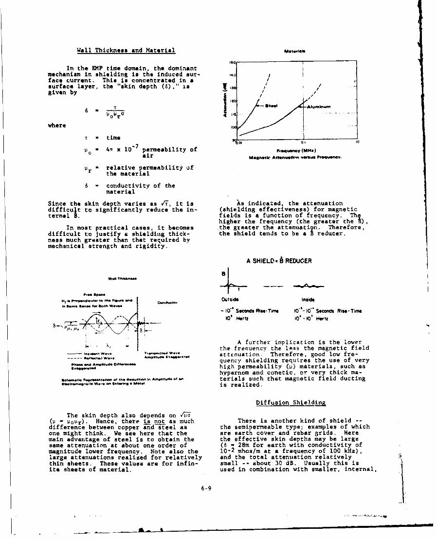
Wall Thickness and Material M.,.IB
ISOIn the EMP time domain, the dominant
mechanism in shielding is the induced sur- 1o0
face current. This is concentrated in a /surface layer, the "skin depth (6) ." is ISgiven by
T oa"t t"ltlm
where - o 1--
T - time I___ _ _ _ _
P0 - 41T x 10-7 permeability of Fsqui .c(MMa)air Ma~nottk- A~utkr vowsu reqmem~4•y,
-r a relative permeability ofthe material
6 - conductivity of thematerial
Since the skin depth varies as /?, it is As indicated, the attenuationdifficu. t to significantly reduce the in- (shielding effectiveness) for magneticternalB. fields is a function of frequency. Th@
higher the frequency (the greater the B),In most practical cases, it becomes the greater the attenuati n. Therefore,
difficult to justify a shielding thick- the shield tends to be a B reducer.ness much greater than that required bymechanical strength and rigidity.
A SHIELDa • REDUCER
wan Thioian~ee
r.ee spece
Hy is P qedlCuler to the FlOw ed Conductor Waldo Insidein Sota* Ren ee f or llot h• W a~e- I0" Seconds R se-Tiot -0 T O I0" " S ,conds Rise-Tim e
10' INrtz 10'- 10' 4 fat" ,,
A further implication is the lowerthe freauency the less the magnetic field
--ef.•tod Amplitude, I A belattenuation. Therefore, good low fre-
"phe" erwd A liodOlfferee quency shielding requires the use of very6,6egra-p high permeability (w) materials, such as
hypernom and conetic, or very thick ma-W,9 senta,•,• of , t. in Ampliu of s terials such that magnetic field ducting
* -to"ei Wo. on enterig a Mel is realized.
Diffusion Shielding
The skin depth also depends onf;- Uor). Hence, there is not as much There is another kind of shield --
difference between copper and •steel as the semipermeable type; examples of whichone might think. We see here that the are earth cover and rebar grids. Heremain advantage of steel is to obtain the the effective skin depths may be largesame attenuation at about one order of (6 - 28m for earth with conductivity ofmagnitude lower frequency. Note also the 10-2 mhos/m at a frequency of 100 kHz),large attenuations realized for relatively and the total attenuation relativelythin sheets. These values are for infin- small -- about 30 dB. Usually this isite sheets of material, used in combination with smaller, internal,
6-9
Al
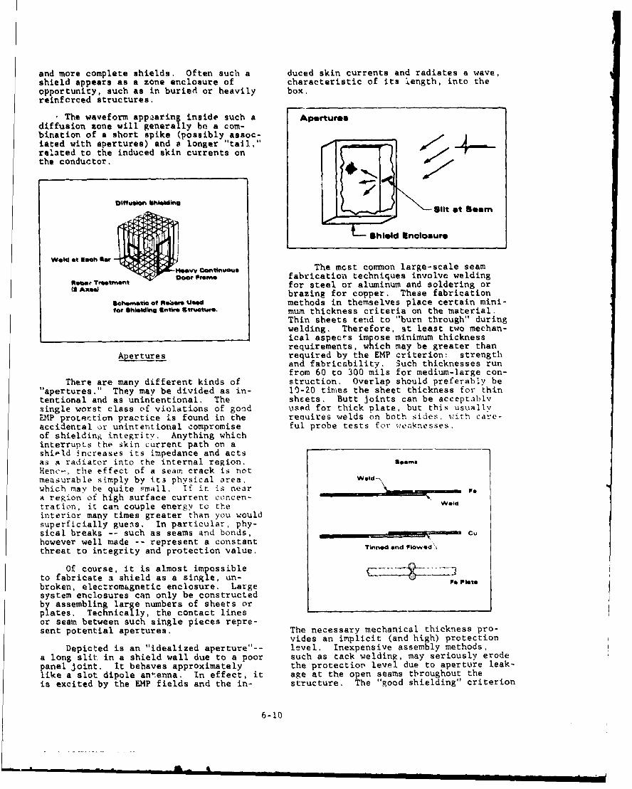
and more complete shields. Often such a duced skin currents and radiates a wave,shield appears as a zone enclosure of characteristic of its length, into theopportunity, such as in buried or heavily box.reinforced structures.
. The waveform appzaring inside such a Aperturesdiffusion zone will generally be a com-bination of a short spike (possibly assoc-iated with apertures) and a longer "tail,"related to the induced skin currents onthe conductor.
Diffusion OhileMIne
Shield Enclosure
Weld at Mesih Ser, cotiuThe mcst common large-scale seam
loor Proms fabrication techniques involve weldingaebe. T.eent for steel or aluminum and soldering or(2Aste) brazing for copper. These fabrication
sieetioo oetOam.Usd methods in themselves place certain mini-o Sldng Entire Stfructur. mum thickness criteria on the material.
Thin sheets tend to "burn through" duringwelding, Therefore, st least two mechan-ical aspects impose minimum thicknessrequirements, which may be greater than
Apertures required by the EMP criterion: strengthand fabriccbility. Such thicknesses runfrom 60 to 300 mils for medium-large con-
There are many different kinds of struction. Overlap should preferably be"apertures." They may be divided as in- 10-20 times the sheet thickness for thintentional and as unintentional, The sheets. Butt joints can be acceptablysingle worst class of violations of good used for thick plate, but this usuallyDIP protection practice is found in the reauires welds on both sides, with care-accidental or unintentional compromise ful probe tests for -weaknesses.of shielding integrity. Anything whichinterrupts the skin current path on ashield increases its impedance and actsas a radiator into the internal region. SeemsHenco, the effect of a seam crack is notmeasurable simply by its physical area, Wel-.which may be quite small. If it is near , e
a region of high surface current concen-tration, it can couple energy tc the Weld
interior many times greater than you wouldsuperficially guess. In particular, phy-sical breaks -- such as seams and bonds, Cuhowever well made -- represent a constantthreat to integrity and protection value.
Of course, it is almost impossibleto fabricate a shield as a single, un- -e Pbroken, electrom&gnetic enclosure. Largesystem enclosures can only be constructedby assembling large numbers of sheets orplates. Technically, the contact linesor seam between such single pieces repre-sent potential apertures. The necessary mechanical thickness pro-
vides an implicit (and high) protectionDepicted is an "idealized aperture"-- level. Inexpensive assembly methods,
a long slit in a shield wall due to a poor such as tack welding, may seriously erodepanel joint. It behaves approximately the protection level due to aperture leak-like a slot dipole an-enna. In effect, it age at the open seams throughout theis excited by the EMP fields and the in- structure. The "good shielding" criterion
6-10
- -- I.• -- ML

may require continuous and meticulous T'he basic mechanical requirementswelding al.ong aT -seams in order to matcb for simple reliable seam bonds are ab-the protecticn value inherent in the ma- solute flatness and electrical cleanli-terial itself. ness. Neither of these is generally
achievable in other than ideal laboratoryAs an example of the welding integri- conditions. The pragmatic hardware prob-
ty criteria, an ICBM test facility had a lem is then to obtain low-impedance con-shielded room built into its base. This tinuous contacts at an acceptable levelenclos,.re had a 100 dB requirement in the of "dirtyness" and "deformation."UHF domain. The construction was suchthat several large structural I-beams Electrically clean surfaces can bepassed through the room. In order to readily obtained with pure tin, gold,seal" the room electromagnetically, spe- palladium, platinum ind silver! Zinc,
cially cut plates were welded around the cadmium, and very thin gold platings arebeams and onto the steel walls. These considered as acceptable substitutes.seam areas were tested by using a trans- Easily oxidized materials (like aluminum)mitter loop outside and smaller receiver should be avoided. Lubricants are capri-loop probe inside. A single continuous cious. In some cases, they will inhibitwelding pass proved inadequate to prevent corrosion and oxidation and facilitateleakage at this seam. Several additional good metal-metal contact. However, motorpasses were needed around these beams, oils, for example, are more apt to doboth inside and out. These were made in just the opposite.such a way as to build up a t'aick weld.The inner corners were parti:ularly diffi- Controlled roughness (machine siningcult points, as indicated here. and knucling) is generally better than
attempting to achieve a smooth surfacefor mating parts. When controlled rough-
Weld Integrity ness is utilized, the total contact areais generally greater, and easily predic-table, than for smooth surfaces which mate
Manetc Steel usually at only three points (no surfaceis perfectly smooth).
Weld Areas
CLEAN CONTACTSExtra Weld
Steel I-Beam GOOD BI.D
TIN, ZINC. CADMIUM ALUMINUM, IRON (OXIDES)
PLATINGS (ALSO GOLD,
PLATINUM, AND SILVER)
THIN - PLATINGS ------ THICK
Magnetic Steel Plates SPEC IAL LUBR ICANTS SULFUR-BASED
ELECTRICAL-*- AND PAINTS -- AND OXIDIZED
SCORED,Gaskets and Bonds KNURLEDL - . SURFACE --------- I ILL-SMOOTH
Considering the difficulties en-countered with such seemingly "tight"apertures as welded seams, it is no sur-prise that metal-to-metal contact sur-faces, held together by simple mechanicalpressure, can constitute serious viola- Roughness is one way to compensatetions of shielding integrity. Such con- for surface irregularity. An ultimatetact areas are unavoidable at functional way to do this is to use deformable con-apertures, e.g., access doors, service ductive gaskets. A good way to under-hatches, equipment panels, etc. stand the pressure contact problem is to
consider a panel seam, bonded by meansThere is extensive literature on all of bolts and flange strips, as illustrated
manners of bonding long, continuous, me- here. In the frequency domain of inter-tallic, contact lines. They deal with a est, seanis of this type require specificrange of bonding permanency, from perma- contact pressures of 60 to 100 poundsnent, once-made joints, through rarely- per lineal inch for 80-100 db attenuation.disturbed service panels, to continuously Obviously, this form of seam is best forexercised doorways. Of course, the latter 'once-only" cases, which are expected torepresent the most difficult problem in be broken very rarely, if ever, duringdependability and maintainability, the syste2m's life.
6-11

Pressure Contacts
Typical Panel Seem
People have also resorted to the"gasket" solution for "bonding" peripheral MISSLE LOADING HATCH Rr SHIELDINGcontacts which would only be occasionally (CLG),(METHOD A)broken. It is also useful for irregularor deformable surfaces.
There are two "fairly" -ood types: The average field attenuation thatcan be obtained with knitted wire mesh
1. The flat molded metal gasket gaskets as a function of the appliedwhich deforms slightly under pressure is indicated here. It shouldpressure. This is a "throw- be noted that application of higher pres-away" in the sense that it sure increases attenuation, but shortenscannot be reused. the lifetime of the gasket as it perma-
nently deforms.2. The braided cord gasket. A
variety of exotic designs ap-pear on the market. Thegood ones from an attenua- 70tion standpoint utilize de- - ,- 1[
formable metal cores. -60 -
Unfortunately, these have Recommended Operoting Pointlow resiliency and can onlybe reused two or three times. - -
40The synthetic core, double ==40------------------
braid gaskets are generally -
more transparent in a given 3 --- ---,- --
geometry. The single braid 30types provide even less atten- Ii Iuation. Braided gaskets are - 20 - - ----....---
not generally recommended for 0---------1exposed, unmaintained situa- OItions for EMP protection, 7 H - , , , -
I ICorrosion control of the gaskets and 0 10 20 30 40 50 60 70
the associated mating surfaces is also a Applipel Pressure (psi)problem. Considerable maintenance is re- KNITTED WIREIMESH GASKETS,quired to insure good electrical contact. AVERAGE FIELD ATTENUATION
Depicted is a typical application of Resilieit finger stock is a favoritea knitted mesh gasket for a ship missile solution for doors and hatches which mustloading hatch. Note that the RF gasket is be frequently used. Finger stock shouldprotected from corrosion by a water seal be used in double rows. Some peopleon the hatch. suggest that the rows should be staggered
for maximum attenuation so that the fin-gers in one are opposite the slots in theother. At the higher frequencies, thisseems reasonable when one considers theradiation pattern of each slot, seen asa tiny dipole.
6-12

Finger stock is probably the most ahielded Enclosuresdifficult protection hardware to main-tain. Traffic inevitably brings with itdirt and abrasion. The doors and frames 24.GAUG, G....NNIAEMARINI-TYPI TL SIT
must be extra stiff if the fingers and PLYW00ooL, C , D10.0,
the contact surfaces are to maintain theirregister.
Finger Stock and Doors f IGalvanized Steel Sheetwith Plywood Core.
Door Wall
PrWlnure Finger Stock
Jamb '
Door_/M WallDoor Fraea C1oppr Shoet
re" Partition Joint Example.Wiping Finger Stock
Copper Sheet
Iron Frame Open Apertures
Door,--1,-- -i So far we have dealt with apertureswhich could be "closed" electromagnetic-
ally by means of conductive materials(sheets) and construction similar to the
____ surrounding shield. The signific~ntproblem was with peripheral. control. Somemechanical requirements, hoever, callfor a physically open aperture for such
The joint constructicns illustrated things as ventilation, mi.crowave lines,here show some of the ingenious ways in .1tc. Two broad classes of "solutions"which shielding engineers have solved the are common for these: screens of variousproblem of structural flexibility with types, and "waveguides-beyond-cutoff."reliable shielding effectiveness. They The latter can also be used sometimestypify shielded enclosures for R.F. test- for entrance passages and doorways toing and measurement. At present, at avoid the finger-stock problem, whereleast, ic is not likely that military sys- penetration of high frequency content istems would employ such components except clearly not a problem.as accessories in production and testingphases. Ordinary heavy-duty screening can
provide on the order of 40 dB attenuation.The prefabricated bolt-together en- The trouble with ordinary screening lies
closure has enjoyed wide acceptance. It in corrosion and oxidation which candoes, however, require periodic mainten- break the contact between individual wires.ance. The frame shifts cause open slits Electromagnetically, an old piece ofand metal-to-metal seam corrosion. Where screening may be a good coupler. Thehigh shielding requirements exist, serious specially fabricated materials likeconsideration should be given to the "electromesh" are treated to resist thiswelded seam enclosure, action.
6-13
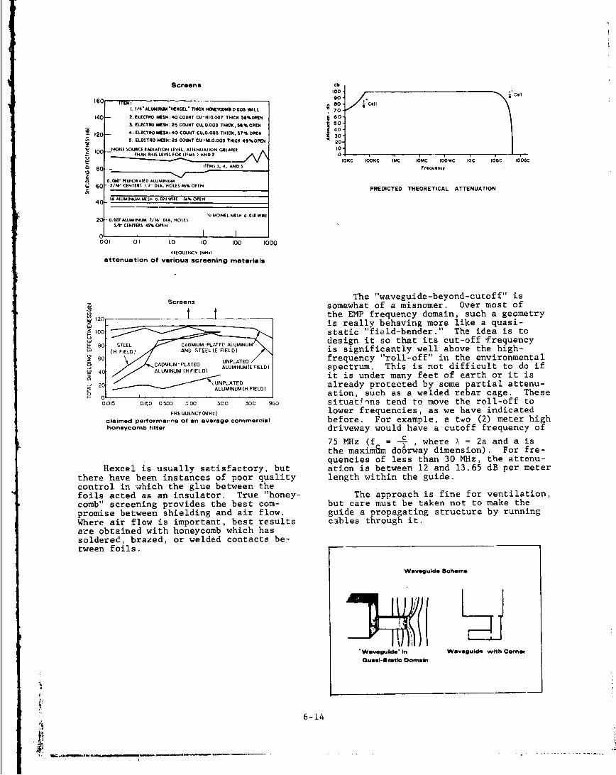
Screens db
160 ITEM; 0.
I. 1/4VALUMIMIN t'MEXCIEL' THICK HO1NEY1O 1 0.003 WALL 70 e
140- 2. ELECTRO MESH:!40 COUNT CU'NIQOOT THICK 3•%OPEN o603. ELECTRO MESH: 25 COUNT CU. 0003 THICK, 52%OPENE 50
40
120- 4. ELECTRO MESH: 40 COUNT CU,O,003 THICK, 57% OPEN 30S. ELECTRO MESH: 21 COUNT CU "NI.O.O05 THICK 41%OPEN 20
___NOISE SOURCE RADIATION LEVEL, ATIENUATION GI( ATEE 10100) -- THAN THIS LEVEL FOE IIRMS I AND 2 01•J ••F V •IOKC IOOKC IM~c IOMC IOOMC IGc IO0C IOOGC
S80 -- IIIM$ 3, 4, AND 5 Frequency
a O,.WO KIIIFORA"E[ ALUMINUM S60 -- 5/16" CENTIES 1"4" DIA, HOLES 4i6% OPEIN6.PREDICTED THEORETICAL ATTENUATION
16 ALUMINUM ME SH 0.020 WIRE 36% OPEN40_
IU MONIEL MESH 0,011 WIRE
20 -0.037 ALUMINUM 7/16" DIA. HOLES/1" CCENTEIS 45% OPtN
001 01 1.0 10 I00 1000
fREQUENCY (MH.)
attenuation of various screening materials
Screens The "waveguide-beyond-cutoff" issomewhat of a misnomer. Over most of
20t the EMP frequency domain, such a geometryis really behaving more like a quasi-
,00 static "field-bender." The idea is toN design it so that its cut-off -frequency, 80 STEEL CArDMIUM" PLATEC ALUMINU
W (H FIELD. AND STEEL (E FIELD) is significantly well above the high-(D DM UNPLATED frequency "roll-off" in the environmental
S•CADMINUM'PLATED ALUMINUM(EFIELD) spectrum. This is not difficult to do ifW 40 ALUMINUM (H FIELD)
it is under many feet of earth or it is20 PLATED already protected by some partial attenu-ALUMINUM (H FIELD)
. .. ation, such as a welded rebar cage. These
0o015 0-1 0500 300 300 300 960 situations tend to move the roll-off toFREQUENCY(MHz) lower frequencies, as we have indicated
claimed performatine of an average commercial before. For example, a two (2) meter highhoneycomb filter driveway would have a cutoff frequency of
75 MHz (f = -_ ,where X = 2a and a isthe maximfim doorway dimension). For fre-quencies of less than 30 MHz, the attenu-
Hexcel is usually satisfactory, but ation is between 12 and 13.65 dB per meterthere have been instances of poor quality length within the guide.control in which the glue between thefoils acted as an insulator. True "honey- The approach is fine for ventilation,comb" screening provides the best com- but care must be taken not to make thepromise between shielding and air flow. guide a propagating structure by runningWhere air flow is important, best results cables through it.are obtained with honeycomb which hassoldered, brazed, or welded contacts be-tween foils.
Wevegulde Scheme
•Wavegulde" In Wevegulds with Corner
Cueel-Satlat Domain
6-14

The use of the "waveguide-beyond- Penetrationscutoff" approach for ventilation shaftsin structures is one typical application.High frequency roll-off is obtained by There are many kinds of "penetra-partitioning the overall opening into an tions." ýIost commonly, one thinks of anarray of smaller openings as depicted. insulated conductor passing into a facil-This will cause some reduction in airflow ity or system. It may be carrying powerdepending on the effective area reduction or functional signals, but uninsulated,of the overall opening. "grounded" conductors, such as motor
shafts, can also represent penetrations.MetalPartit•-onsIN .razed0,r Thus, there are two broad classes -- elec-Soll At Eac~h intersection trical and mechanical. We see here ways
in which each can provide paths for coupl-Clou C t sIs (Sqr--•OrHecsiogonc) ing and transferring energy from the ex-
ternal to the internal zones. Noteorkimu Cl Openiný X/3 I.--particularly that mechanical penetrationsO1 Highest Frequency (Shortest can be deceptively protected by innocent-
- - - Wavelength) TO Be Attenuated looking bonds, which are really high-
- - -l ±4Himpedance couplers.
Depth Of Closed Cell DependdsOn Ratio Of OperatingTypical Eleient Frequency To Cut off
Frequency Of Cell And Atteinution
Required. Nominal Depth Is5 Tims Largest Opening ForIOOdb Attenution.
Penetrations
Cabinet Mesh Gasket Dc
a)Bolted Ilstallation b) Welded Installatio, Egectrical Mechanical
USE OF HONEYCOMB MATERIAL FOR SHIELDING AIR VENTS
Another technique to handle large The existence of a true "electricalapertures, such as personnel entry ways penetration" corresponds to an intentionalinto shielded compartments, is through or unintentional violation of the zoningthe use of a protected entry. Shown is concept. If an electrical circuit isa technique using a double shielded door carefully confined to a single EM zone,hallway type configuration. Interlocks then its penetration through a shield doesshould be provided if critical equipments not, in facc, constitute a violation. Inare housed in the compartment so both principle, it cannot transfer energy whichdoors cannot be open at the same time. would not be there in its absence. We
make this seemingly simple point to empha-size the necessity for observing zonalhierarchies in providing conductor andcable shielding (as discussed in a suc-
--------... •Iceeding section).
•,r But what about unavoidable conductorShtwed Area c•,tong penetrations -- such as, for instance,crtol Equipment long wire antennas? One thing to do to
rectify sich situations is to provide en-Dol trance protection in the form of filtersDoubIe Door
tiallyTypo or active devices (zener diodes, sparkEnt't gaps, etc.). These are discussed in the
ui section on "Protective Devices." These
protective devices should be located invaults or smnall shielded boxes.
Since all external conductors arecollectors of EMP energy, they must all
horsS,,.rll , Locaed a Fom be terminated at the entry to the shieldedCorr,dor Cu .0arrg Ertry ToHardened Arso compartment (or equipment cabinet). If
DOUBLE DOOR HALLWAY TYPE ENTRY TO these terminations are allowed on a hap-HARDENED AREA hazard basis, (terminating on all sides
6-15

of the enclosure), they will inject addi- We noted before that a conductiverLonal current on the enclosure resulting metallic penetration may be deceptivelyin higher fields on the inside. There- protected. Consider, for instance, afore, to keep this energy from entering, shaft passing through a bushing. In theall penetrants are brought into the pro- case of a metallic shaft with a conductivetacted space via a single point of entry bushing and a bond strap, it can be createdinto an entry vault. The conductors analytically as a parallel R L circuit(pipes, condu!'7, cable shields, etc.) are as shown. Simple circuit analysis can beperipherally welded to the enclosure at applied to determine the fraction of thethe entry point. All protective devices current which is not shunted by the bondare contained in the vault and the out- strap or the bushing resistance. If theput electrical leads into the enclosure bushing has a high contact resistance (orprotected by feed-through capacitors, for is an insulating bushing), at high fre-example. These terminal protection ap- quencies (WL > R) the shaft can act as aproaches are discussed in subsequent para- probe antenna-coupling directly to thegraphs of this section. interior as a skin current or by reradi-
ation. This type of penetration couldeasily result in a 30 dB lead in a 60 dBshield.
In the case of a nonconductive shaft,s$.I C\twots wo the configuratior can be modeled for anal-seemnr 10,11, vysis as a dielecý.ricallv loaded circular
S\. @Ma aperture. The aperture problem becomesrw t0lds Or important when the aperture diameter isWild At bkoh _ li.hfsTOW equal to or greater than the half wave-
length of the highest frequencies assoc-w iated with the incident waveform. For
P -e o r small shaft dimensions (5 to 10 cm), theI: coupling through the aperture would be
f ,ee In T Sacesmall (a few dB) over the frequency spec-Shal, Af.i. trum of the EMP.
"Mechanlicl Penetratlon.
1111.hing Conteot Ptuaimance
TYPICAL CIMP HARDENED SPMCE Shield nt %MP
Voltege O.neretor
ech.nic.l orive
Finally, one can isolate that por- o.nd ,.d-ct..cetion of the system (which really goes Ap.. .... Equi.vlnt Cirit EquWventback to systems and circuit layouts) andsimply make its terminal circuits veryhard.
So we see that the treatment of pur-poseful electrical penetrations is not The principle here is to "rectifyreally a "shielding' topic. the obvious." We will discuss some em-
bodiments for these first two types offixes.
ELECTRICAL PENETRATIO Treatment
NOT REALLY A "SHIELDING" 0 Break the metallic pathHARDWARE PROBLEM -- WHY?
* Improv, the meal bondZONE VIOLATION - GO TO "SHIELDED"
E Examine electromechanical servos, relaysENTRANCE PROTECTION -b GO TO "PROTECTIVEDEV ICES" plus filters on the wires]
TERMINAL HARDENING -- 01G TO "SYSTEM ASPECT" 0 Examine non-conductive, exotic schemesAND "COMPONENTSUSCEPTIBILITY"
6-16

The first approach is to break themetallic path. This treatment replacesthe continuous conductor by a small capa-citance. Its equivalent circuit represents |mproveThealold
it as a filter between the two EM zones.Note that the separate small enclosure must Toper"d Look Bushing
be well-bonded to the shielding partitionbetween the two zones. An impedance atthis poi'at turns it into an effectivecoupler. This is equally true for filters Ad.tei•mla
and for other enclosed protective devices MetalBraided BMelocated at a partition between zones. Analternative approach is the use of thewaveguide-beyond-cutoff technique. This Switches
approach requires the mechanical shaft tobe non-conductive. In sizing the wave-guide, it must be analyzed as a dielec-trically loaded guide with the dielectricbeing the mechanical shaft.
In "explosive proof" hardware, or inequipments with very high shielding re-quirements, a simple fix is to utilize abraided metal bag to increase the shield-
Break the Metallic Path ing as shown.
Good Better
Insulated Coupling Conat Pstic shaft GroundingBushing&
The primary purpose of grounding isS• the protection of personnel and equipment.Electrical codes require that electrical
and electronic equipment cabinets/framesbe connected to the surrounding media
Length (building, earth, etc.) in such a mannerEquvalent Correspondst -to that no shock hazard exists due to a volt-
Circuit "Waveguide age difference between the equipment andI Bevond Cutoff the surrounding media. For equipment pro-
NO-NO!-- Criteri"e tection, the purpose of the ground is toprovide a fault current path so sufficientfault current can flow to caiuse circuitbreaker or fuse actuation. Ground furtherprevents the buildup of electrostatic ortransient voltages that may cause insu-lation damage. Lightning protection is a
Shown are two examples of unusual special case of transient voltage builduptreatment. A simple way to improve a which is shunted to ground, in most cases,leaky manual adjustment shaft is to mount via surge protective devices.it through a split-bushing with a taper-thread locking nut. When the locking nut In other words, the purposes ofis tightened, a low resistance bond is grounding are to provide an equipotentialachieved between the shaft and the equip- connection between equipments and surround-ment panel. ing structures/media, and a return current
path for fault currents. For signal cir-cuits, two-conductor transmission linesare used. Tying the signal circuit toground prevents electrostatic drift andprovides a common reference provided theground circuit is truly an equipotentialplane.
The discussion which follows willdivide the grounding problem into earthgrounds ("exterior" grounds), and equi-potential or reference nodes ("interior"grounds). Emphasis will be placed onmeeting system grounding requirements with-out becoming a major source of EMP pickup.
6-17

the conductor. The inductance term pro-duces an IZc drop (conductor impedance),in addition to the IZ (ground impedance).
Both Interior end Exterior Grounds are The groundwell impedance can be reducedNeeded for Other System Reaulrements by using large contact area ground rods
or wells and improving the conductivityof the earth in the immediate vicinity
Both Interior end Exterior Grounds can by "salting" (ionic salts). Further,bee Major Source of EMP PICKUP most of the EM energy in a current carry-
ing conductor exists in the field externalto the conductor. The impedance mismatchresults in the field stored energy beingreflected and reverberating on the con-ductors.
Earth/Exterior Grounds
There ar-e at least three reasons for Ground Resistance and Transient Impedance
considering how EMP and exterior groundsinteract. First, there are long wave-length threat components with which groundcircuits can meaningfully couple. Second,system grounds are essential for any num-ber of other reasons; hence, their EMPcoupling is a germane issue. Third, ithas been pragmatically established thatgrounds make a noticeable difference.-- Abmomllongood and bad -- in nuclear test and nuclearsimulation instrumentation. Most of the Transiemt Fied energy
is Outside the Physical Conductor,
Of course, a grounding system can beput to advantage in EMP control. But this _
needs to be integrated with other ground-ing requirements, i.e., lightning, power,etc. One demonstrated use of controlled
grounds was found during atmospheric test-!he basic idea of earth grounding is ing, Here, long duration reverberation
Trovide an equipotential distribution currents on the exterior of the cablese th tructural members of a sys- were present which often interfered with
t.Ži and t-x 4 urrounding natural environ- shock wave measurements which occur a few.. nt. This concept is perfectly valid milliseconds to seconds after the blast.,.nly for the ideal case of static fields,infinite earth (ground) conductivity, and By viewing the long cable run as ano current flow. Thus, earth grounding transmission line and terminating it inis an attempt to connect, in a field- its Zo, much of the reverberation couldsignificant way, to the large, but poor, be suppressed,conductor. In the cases of shock hazardelimination or lightning protection, onlylower frequencies are of interest and this"equipotential sur ace" concept must onlyapply for local areas. Fox EMP, on theother hand, nherc 'tributed systems areof com ý,, rhis . -- •pt must apply overlarge gý,graphiL-.i. areas and over a broadfrequency spectrum.
Another factor is the connection fromthe system structural members to the earth.The idea is to cour 'he electromagneticenergy into the ear nd absorb it in the iru-jiL-earth. The impedF co earth is a func-tion of the connecLion from the system tothe groundwell, and the impedance of thegroundwell to the earth. To minimizevoltage buildup due to EMP or other trans-ients, these impedances must be low at allfrequencies of interest. All conductors T 7 1,have associateJ with them in inductancewhich is a function of the geometry of
6-18

This EMP cable ringing suppressioncalls for a resistance (10-200 0) in *2series with the ground lead. This is com-
patible with other exterior grounding re-quirements. Most grounding systems require System Connectiona low (<< I ohm) impedance earth connection.In power systems, impedances of 10-200ohms would significantly reduce fault #1currents possibly inhibiting the operationof protective elements. Further, thefault currents would result in a largevoltage appearing between the equipmentand earth creating a potential shock haz-ard to personnel. This latter problemwould also exist for lightning grounds.Even communication system's antennas re-quire low impedance ground connections Equivalent Circuit(earth counterpoise) for good radiationefficiency.
For power protection, the use of a The concept of a single point groundchoke shunt with low 60 Hz Z, but high is to tie all system elements to a commonEMP Z, can be a compromise for lower power central ground point, thus eliminatingusers, the ground loops. These "straight" cable
runs can also pick up EM energy. SinceTherefore, good earth connection the earth is a finite conductor, an 'E'
(i.e., low Z) at all frequencies of in- field exists along the ground leads whichterest (EMP or other transients) will induces a potential gradient along theseprovide local protection of personnel leads. If these ground leads are longfrom shock hazard, equipment protection (>100 meters or so), a local shock hazardin terms of insulation failure, and fault exists, Further, since the ground leadscurrent protection. have inductance, a high surge impedance
can exist which would cause problems inAnother factor to be considered in lightning prctection and fault current
designing a grounding system from an EMP protection. The voltage induced in theviewpoint is EM energy coupling into sig- ground leads can be calculatednai circuitry via the ground system. Twogrounding systems philosophies have beenexpounded in the literature: (1) themultipoint grounds, and (2) the singlepoint grounds. In either case, EMP caninduce substantial amounts of current flowonto the shields of various portions ofthe system and the interconnecting cablesor conductors.
In the case of multiple point ground- #21*ing, ground loops which can couple EM en-ergy through Faraday induction are formed.The voltage induced in these ground loopsis equal to the time rate of change of the tLmagnetic field and the area of the loop(Vg = BA). While such a grounding schememeets all the requirements for personnel Zgsafety and equipment protection, it doesnot meet the EMP requirements. The volt-age induced in these ground loops appears Equivalent Circuitas an offset voltage for signal circuitsthat utilize system ground as a reference, And Is Given By:This can result in upset, and in some V, J Egdicases, damage to sensitive circuits andcomponents. Note If
V rdV 1UVI-G 2-6 3-G
6-19
.. £
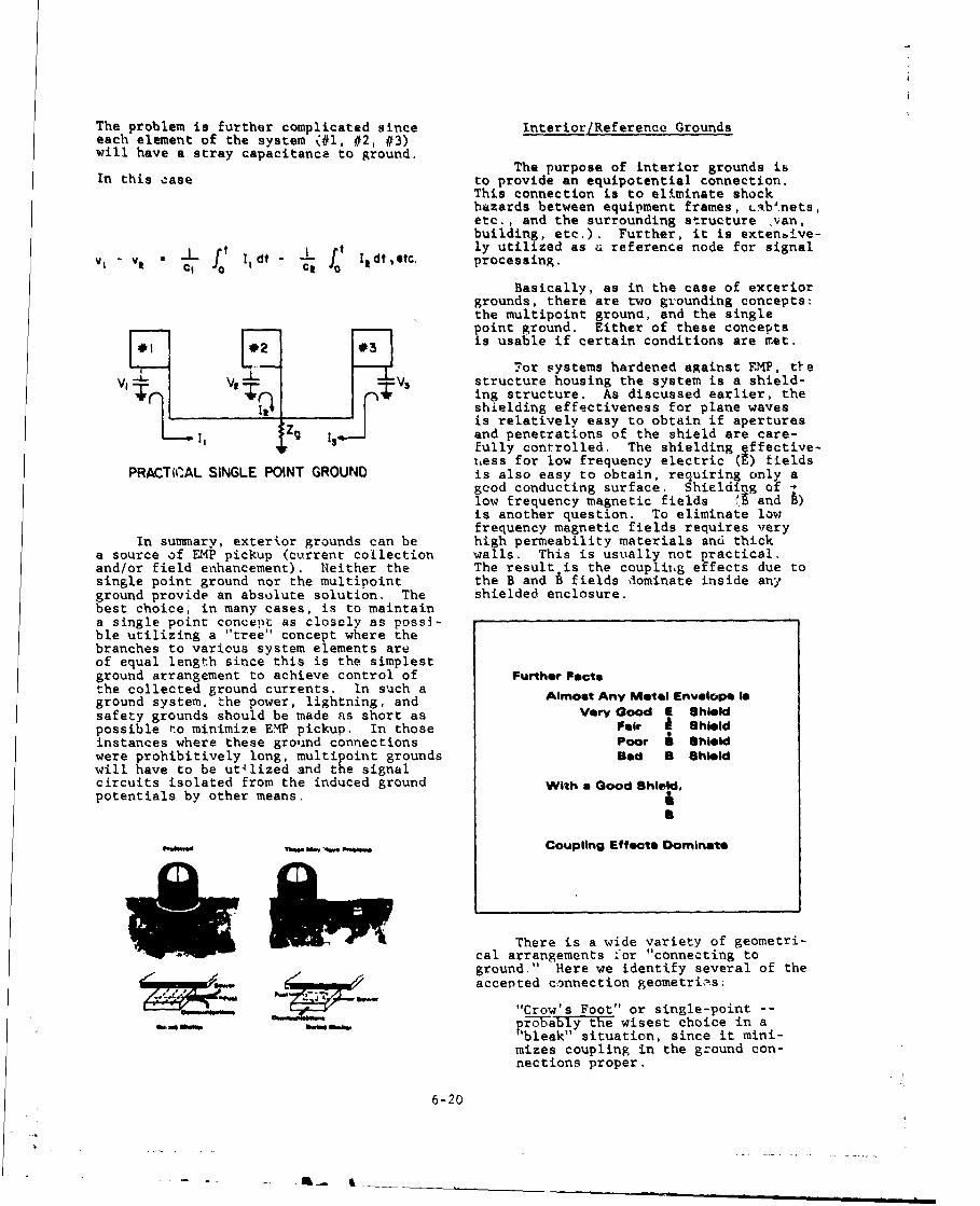
The problem is further complicated since Interior/Reference Groundseach element of the system (#1, #2, #3)will have a stray capacitance to ground.
The purpose of interior grounds isIn this case to provide an equipotential connection.
This connection is to eliminate shockhazards between equipment frames, LAbVnets,etc., and the surrounding structure van,building, etc.). Further, it is extenbive-
I ~tly utilized as ei reference node for signalV v= t 1 dt I ,dtetc processing.
Basically, as in the case of exceriorgrounds, there are two grounding concepts:the multipoint ground, and the singlepoint ground. Either of these concepts
#2is usable if certain conditions are met.
7or systems hardened against FMP, t1eV1 V- V3 structure housing the system is a shield-
ing structure. As discussed earlier, theshielding effectiveness for plane wavesis relatively easy to obtain if apertures
Zg 13 and penetrations of the shield are care-fully controlled. The shielding iffective-itess for low frequency electric (E) fields
PRACTiCAL SINGLE POINT GROUND is also easy to obtain, requiring only agood conducting surface. Shielding oflow frequency magnetic fields (1 and A)is another question. To eliminate lowfrequency magnetic fields requires very
In sunmnarv, exterior grounds can be high permeability materials and thicka source of EM? pickup (current collection walls. This is usually not practical.and/or field enhancement). Neither the The result is the couplii.g effects due tosingle point ground nor the multipoint the B and A fields dominate inside anyground provide an absolute solution. The shielded enclosure.best choice, in many cases, is to maintaina single point concept as closely as possi-ble utilizing a "tree" concept where thebranches to various system elements areof equal length since this is the simplestground arrangement to achieve control of Further Factsthe collected ground currents. In such a Almost Any Metal Envelope Isground system, the power, lightning, andsafety grounds should be made as short as Vary Good 9 Shieldpossible to minimize EM? pickup. In those Fair Shieldinstances where these ground connections Poor S Shieldwere prohibitively long, multipoint grounds Bad B Shieldwill have to be ut 4 lized and the signalcircuits isolated from the induced ground WithaGoodShield,potentials by other means.
Coupling Effect* Dominate
There is a wide variety of geometri-cal arrangements for "connecting toground." Here we identify several of theaccepted connection geometri;,s:
"Crow's Foot" or single-point --_ *ro prably the wisest choice in a
'bleak" situation, since it mini-mizes coupling in the ground con-nections proper.
6-20
-. . .. . --

Fishbone -- the Lower level (high- In large facilities, since theer sensitivity) circuits should classical "star" or "crowsfoot" is -otusually be at the "far end," where practical for the reasons discussed, it"ground currents" are lij.,er, is often replaced by a "TREE" system.
The "TREE" system is a combination ofMultipoint -- note the opportunities Faraday shielied zones, each utilizing arrground loops and common impe- classical "star" system ground, for sig-dance IZcommon voltage rises. nal reference and local hazard, with the
local Faraday Lhields grounded to theFloating Grounds -- often employed nain structure ground. These zone groundswhere a single point ground is int- are for safety ground only and signalpractical and where a nultipoint grounds are isolated by the zonal shieldsystem could cause trouble. Here, connectiotis. These grounds may be ob-each subsystem case assumes its tained by ground buses or directly toown potential without ill effects, the conducting structure depending on theprovided that good isolation faLllity geometry. Signal connections(common-mode rejection) is real- between zones must utilize wired returnized. and not provide additional ground paths
between zonal shields.
Interior
Building Envelope Shield
Many of these configurations workvery well if the ground lead length isshort compared to the shortest wavelengthof the penetrating fields, insofar as Circuit Considerations - Circuit Couplingcoupling energy into the system via theground leads. The multipoint ground alsoprovides for loop coupling. An addition- There are three predominant ways inal problem that can exist with the multi- which EMP energy gets into circuits: (1)point ground is that each element of the B -dot doupling, (2) terminal injection,system is not tied to an equipotential and (3) direct injection. The effect ofsurface, that is, if the surface is the A coupling can be analyzed as equivalentenclosing structure, it may not be at a to distributed circuital voltage input.single potential due to bad seams, etc. Terminal injection appears as extraneous
voltageor current pulses at the peripher-All ground leads also exhibit an al equipment terminals. Direct injection
impedance, usually inductive reactance, results via a mutual coupling element,which varies with frequency. This re- such as a "multipoint common ground."stricts the use of the single point groundas a reference ground, especially in Circuit VMP can also be directly in-large enclosures where these ground leads duced by E-field coupling or by EM radi-may be quite long. This would introduce ation exposure (antenna effects), butreference level voltage offsets between these are usually not important in en-various portions of the system. To elim- closed, well-shielded systems. One shouldinate these reference level voltage off- also distinguish those situations insets, isolation of the signal circuits can which EM or E-field coupling induces cur-be utilized as shown by the now-conducting rents (or voltage) which subsequentlytransmission circuit or the balanced cir- couple by B-dot or conduction effectscuit (floating ground system). (internal zone conversion).
k 6-21
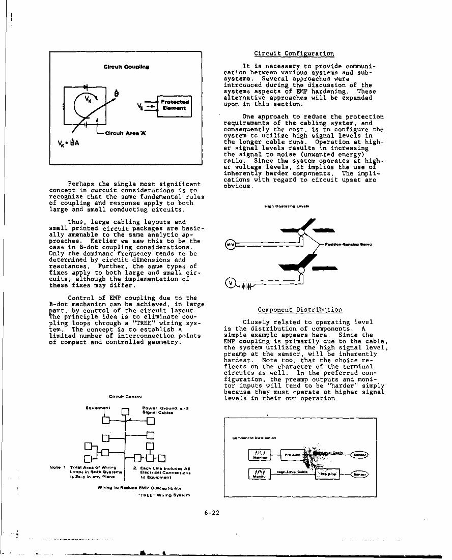
Circuit Configuration
Circuit Coupling It is necessary to provide communi-cation between various systems and sub-systems. Several approaches wereintroduced during the discussion of the
flTT1 • systems aspects of EMP hardening. Thesefv alternative approaches will be expanded
/o 00 Potect upon in this section..L --1 1 One approach to reduce the protection
requirements of the cabling system, and
consequently the cost, is to configure theuit Ar system tc utilize high signal levels in
VXa 6A the longer cable runs. Operation at high-er signal levels results in increasingthe signal to noise (unwanted energy)ratio. Since the system operates at high-er voltage levels, it implies the use ofinherently harder components. The impli-cations with regard to circuit upset arePerhaps the single most significant obvious.
concept in curcuit considerations is torecognize that the same fundamental rulesof coupling and response apply to both High Operating Levels
large and small conducting circuits.
Thus, large cabling layouts andsmall printed circuit packages are basic-ally amenable to the same analytic ap-proaches. Earlier we saw this to be the Mrcase in B-dot coupling considerations.Only the dominanc frequency tends to bedetermined by circuit dimensions andreactances. Further, the same types offixes apply to both large and small cir-cuits, although the implementation ofthese fixes may differ. V 7111-14"
Control of EMP coupling due to theB-dot mechanism can be achieved, in largepart, by control of the circuit layout. Component DistributionThe principle idea is to eliminate cou-pling loops through a "TREE" wiring sys- Closely related to operating leveltem. The concept is to establish a is the distribution of components. Alimited number of interconnection points simple example appears here. Since theof compact and controlled geometry. EMP coupling is primarily due to the cable,
the system utilizing the high signal level,preamp at the sensor, will be inherentlyhardest. Note too, that the choice re-flects on the cbaracter of the terminalcircuits as well. In the preferred con-figuration, the preamp outputs and moni-tor inputs will tend to be "harder" simplybecause they must cperate at higher signal
Circuit Control levels in their own operation.
Equipment Power. Ground, andSignal Cables
Ce .. ... 01o-tlb.l-
Note 1. Total Area of Wiring 2. Each Line includes All -- -LOOpa in Roth Sysems. Electrical Connections I, , Hi...-Lay. C- "is Ze~o in any Plans to Equipment M@mlt_
Wiring to Reduce EMP Susceptibility
TREE" Wiring System
6-22
ga

Another hardening technique is to go mation to be transmitted. Therefore, itto carrier frequencies. Many sensing and is appropriate to discuss the various as-control situations lend themselves to this pects of cable design.by relatively inexpensive terminal hard-ware -- provided this choice is made soon When one examines the possible permu-enough. Due to the added cost usually tations of cable component choices, it isassociated with this approach, its use in obvious that no detailed case-by-caseEMI has been limited. However, addition- evaluation is possible. Rather, we canal criterion of EMP hardening could easily point to certain preferable choices intip the scales in favor of carrier systems, each category of component.rather than dc or low-level, self-gener-ating circuits. These can be broken up into two broad
categories: those aspects which influ-Carrier systenis have the advantages ence the control of the effect of external
of permitting floacing balanced conductors, environment, and those which control thenarrow band-pass filtering, transformer inner cable environment, circuit inter-isolation, easier nullification, and much coupling, and so forth.more.
A simpis Circuit Er.vpie Cable Types
cCrraer lyeTmp
C lnor
* Outer jacket none. insulating
* Outer conductor : none, solid, braided,
wound stripE Inner conductors: single coax or t,-in biax
separate circuit typesinner coaxa, twisted peairs.
Narrow-lind multi-conductorFlits,~rle
e Inner shields none. braided, thin stripinsulated. non-insulated
The carrier frequency chosen to im-plement this approach should be wellabove the highest frequency of the inci-dent EIP spectrum. This provides for the Consider control of the effect ofuse of high pass filters with good roll the external environment, that is, theoff characteristics. Spurious responses reduction of the energy which diffusesbelow the nominal cutoff frequency of the into the cable. This is accomplished byfilter must be carefully controlled, providing an overall shield or, the cable.
These shields may vary from a single lay-Carrier systems, of a more sophisti- er braid type covering, to a relatively
cated nature, may employ dielectric wave- thick solid outer conductor.guide operating in the microwave spectrumor optical data links.
Generally, the EM? susceptibility ofa cable system is related more to the sen- OTRW WFsitivities of the terminal elements and
circuits than to "breakdown" or "burnout"limits in the cable itself. This points ",.wil
at once towards terminal protection and Idwe will say much more about this, but acircuit designer may be able to improve I Amatters by keeping EMP in mind when heconsiders the terminal element design and
the circuit routing through the cable &A Kk ITRE
system.
Cabling Design - Cable Types
Transfer impedance was discussedIn many cases, hard wire intersystem previously in the analysis section, but,
connections are the only alternative due for completeness, we will consider itto cost constraints, or the type of infor- again in context of cable design.
6-23

If the wires of an unshielded bundle For buried systems, a techniquealso interweave, then the "surface cur- which is often desirable is to use arent" due to EMP exposure gets transferred conducting as phalt as the outer protectiveinside and all of the circuits share in jacket over the shield. This conductingits pickup. A braided shield also behaves jacket helps to prevent build-up of thesomewhat like this. Besides having holes current wave. Energy induced away fromfor field leakage, the braid wires trans- the terminal end of the cable is dampedpose. The wire-to-wire contact is not in this manner.very effective and much of the surfacecurrent gets inside, to radiate into the Here is an additional illustrationinternal cable zone. of "good-bad" choices from the EMP stand-
point. Like normal enclosure shielding,l0-2 As an example, an RG-8/U cable has a the thickness is not very critical. One
current transfer ratio or transfer finds that the emphasis is rather onimpedance, for sub-microsecond pulses. shielding "tightness." Again, we want noThus, at the end of a 50 meter length ex- "cracks" if at all possible.posed to a field pulse which induces 10+3amp3 peak current, there will be about a One form of "nontightness" is that50 volt signal on the inside, represented by a spiral-wound strip --
even the double-layer variety. The troublehere ,s that each turn is actually a turnin a loosely coupled continuous mutual
BraldTransperency inductance. The contact resistance alongthe overlaps is too high to avoid somevoltage buildup per turn. This type of
1000 Amps shield acts as a relatively good couplerbetween external environment and internalwires.
50Volt*Oute.r Sh.Id Coml-,ut.on
So' d Metal Wire Strip Laid Oouble Braid
Meet L.ngthwis. I Fiat Strip n Wilasnd
Use of a solid outer conductor re- X- toTo., I Clas.WireO r-I.id
sults in a much lower value of transfer Better __od
impedance at the higher frequencies (above I
approximately 1 Miz). This would resultin much lower coupling to the interior Non*
cables (wires). The thickness of this bad
outer conductor, however, is very impor-.tant at the low frequencies. The outer SpirlWoundStriP S:naI..op..
conductor must be several skin depths Poor Wire Brad
thick at the frequency of interest to Fair
achieve 60-80 dB of shielding effective-ness. This can be accomplished by a choiceof an outer conductor permeability and Conduit, wnen properly installed bythickness. threaded connection or welded joints, be-
haves very much like an additional solid-metal outer conductor, When needed for
Why is the "Exterior" Importont? other reasons, such as blast resistanceor code requirements, it is inexpensivein terms of added EMP cost.
These problems can be compounded byloose material specifications, poor qual-ity control, and lax acceptance criteria.Often, cables are delivered with the out-er shield badly oxidized or even corroded.If the construction of the shield is suchtriat good shielding depends on good in-
"ThickC CnuT ternal contact, it will not be acceptable.Conductor Conducto
In most cases, the outer conductor(shield) is covered by an outer protectivejacket. Lead sheathing or neoprene Jacketsseem to provide cable lifetimes that are
6-24

commensurate with normal system life. Cable Terminal TreatmentThere is some evidence that the insulatedouter jacket: reduced the coupling forcables in direct field exposure, as com-pared with no insulation. The conductiveouter jacket, as mentioned previously, ..... und.
can provide propagation damping for con- -GridPin**
ducted components of current induced froma distant point. From a cost standpoint,neoprene is the favored approach.
Another way of achieving the propa-gation damping effect, which has been used The Waylta OftenDonein some nuclear test programs, is to useconducting baffles. The idea is to radi-cally change the impedance of a cable overa ground plane resulting in reflectingthe energy at the impedance discontinuity. Pine
An example of this effect is the entryway for electric power where tne over-head transmission line (wire over a ground EqulvalentCircuitplane) enters a facility via conduit, thetransition being made at the power pole. The cable shield (outer conductor)The impedance discontinuity reflects an should make good peripheral contact toappreciable amount of energy. the connector shell, and hence, the shell
to equipment enclosure to eliminate thisCoupling of the propagating energy problem. Providing a pressure fiL be-
into a lossy material can also be used as tween the connector shell and mating thea means of propagating damping. This has connector to the enclosure via the appzo-been implemented in the form of ferrite priate bulkhead connector, the transferbeads or cylinders around the outer con- impedance was reduced to 5 mQ at 0.1 MHz,ductor or, in. some cases, single wires 70 mQ at 25 MHz, and 300 mQ at 100 MHz.(either electrical or mechanical use), It For comparison purposes, the cable nor-essentially provides a lossy filter. mallv used with the connector tested has
a transfer impedance of 11.4 mo to >1.0 Qover the frequency range of 0.1 MHz to
Termination of 100 MHz.the Outer Conductor
To preserve the protection providedby a good cable shield, it must be proper-ly terminated at the entry into a shielded PLUGS AND SOCKETS
enclosure or equipment cabinet. Past, andin many cases present, practice is to pro- Or VrKviQe the shield connection via one or more Pros ,. ssw,,
pins of a multiconductor connector. The Shiel
reason for this was, in many instances, .]_,rrWedl Around
the connectur shell was nonconducting. p,,, ltiMost connectors are made cf alumintm Equivalent Circuit- CuCoecoIwhich, in many cases, was annodized for.• "="1"corrosion protection. The effect is toinsert an inductanc2 in series with the Couing
outer conductor which prodtuces a series Ato.now' 'Possobe' 'est,v,.ltage drop and couples capacitively to heGround Ctontct Plu• Ring Contoac SoiidShieldAnd Weld
the other conductors. On a transfer im-pedance basis, this type of terminationwill exhibit a transfer impedance rangingfrom 50 m2 to 10 : over the frequencyrange of 0.1 fliz co 25 Mfz.
This indicates that peripheral bond-ing is the best solutior. Soldp':ing orwelding the outer shield directly to theenclosure wall would further reduce theconnector transfer impedaLce. This isonly cost effective and worthwhile forcables with better shielding effective-ness than the previous case.
6-25

As we hinted before, when properlyinstalled, conduit is easily the best"outer shield" for cable systems. The Twisting and Shielding
principal problems arise at segment con- ..tacts, of course, Again, cleanliness and /careful assembly are essential. Rusted I/oatingo ---Ing-
and corroded threads and bushings willintroduce series impedances along the \\ / -
conduit's length. Welded joints are besc, Good
but expensive.
Welding is almost the only dependable r ------way to deal with the conduit terminals. 1 . ,---Normal clamp rings make contact at only ai .few points, at best. All too often, thereare so.ae loose ones left behind. The con- B .etteo r-duit ends are particularly sensitive sys-tem points, because here the exteriortransmission impedance changes. Pulsecurrents flowing on the outer surface mustbe redistributed onto the equipment shield.
If relative movement between exter- As indicated before, if a systemior conduits and shielded buildings are lends itself to carrier techniques, thenexpected (due to shocks or earth move- we can gain 30-40 dB in protection valuement), the use of bellows, convoluted by using balanced cable circuits withsections, or multiple knitted socks should terminal isolation transformers. Converse-be considered. ly, the requirement on the built-in cable
shielding may be that much less severe.
Internal Conductors The advantage of tl-e "carrier" ap-proach resides in the ease of obtainingbalanced isolation transformers that op-
There are two basic cable construc- erate over a "limited bandwidth." Extrations which are of interest: (1) the co- filtering may also be required to assurea-cial cable, and (2) the multiconductor that the bandwidth is restricted to thepaired cables. Coaxial cables use the "limited bandw'idth" of the transformer.shield (outer conductor) as the signalreturn. Pickup of extraneous signals isprimarily due to tbo transfer impedancemechanism for well constructed cables. .*,*.w,•,,o,.,anCable eccentricity can also result incoupling of magnetic fields but is lessprominent. Good coaxial cable design, Ifrom an EMP coupling viewpoint, is pri- i- __Imarily an effective shield design. As --- ,---discussed in the previous subsection, thebest shielding effectiveness can be ob-tlined with a solid outer conductor. If r ---- I r------cable flexibility is required, double i ------ I I
braided shields can provide satisfactory -------I------performance if properly designed. -----
For medium-level sensors and medium- L----- . .-------J J J
bandwidth circuits, adherence to zoningand circuit reference criteria may sufficeinternally. This dictates provision ofseparate return reference wires (independ- Multi-layered shields is a good ap-ent 2-wire circuits) which are fabricated proach for sensitive circuits. However,as a twisted and shielded pair. Braided if the shields are not properly terminated,shielding is often sufficient here. Broad- the coupled energy will reflect from thely, these practices are generally conmuen- terminal ends of the cable, resulting insurate with requirements for intercircuit additional penetration of the cable. Twoisolation ("cross-talk"). approaches are shown: (1) terminating
the inner shield in dissipative loads,The single reference connection bond and (2) isolation of the shields. To de-
is not as desirable as a continuous metal cide the means of terminating the shields,backshell connector which grounds the it is good practice to consider the multi-cable shield to the subsystem shield with- layer shields and common-mude circuits asout introducing*apertures or high-impedance independent transmission lines and termi-connections. nate them accordingly.
6-26

As discussed in Section IV, the low- certain frequency bands. These approachesest energy coupling is achieved for a non- may be used singularly or in combinationcarrier system by the shielded twisted (hybrid devices) depending on the systempair. If care is excercised during cable and/or protection requirements. The ideaconstruction, good common-mode and dif- is to pass only those signals, in termsferential mode protection can be achieved, of amplitude or frequency, that are re-
'quired for normal operation of the cir-* g Some "connections," such as power cuit.$supply and control circuits, must be dcor non-carrier ac. If these can bet"'eated by means of terminal filters andbw high-level operation, then (togetherwith carrier signal techniques) the EMP Clr-ult'ao1.*.onrequirement on the total cable packagecan be a minimal one. __o.o ":
Protective Devices and Techniques
The discussion to this point has -•been concerned with system Drotection by D--ir-dkeeping the energy out of The system; that -. s,,r.
is, throligh the techniques of reducingthe coupling and shielding. These ap-proaches are nece!ssary for hardening a Pass On On'y W'lA~.'s 644ded.system; however, they only vedetce theamount of energy entering the sysrem.Completely eliminating coupling to orultimate shielding of a system is notviabla.
The result is that some energy will Spectral Limiting bevicesenter the system which may effect theperformance of the system. The use ofprotective devices at the equipment termi- These devices are utilized to sup-nals is another means of hardening at the press certain frequency compcnents of thesubsystem/circuit level. EMP induced signal. In considering spec-
tral limiting devices, the waveform ofProtective devices are used to divert the induced signal must be considered.
or dissipate the undesired electrical Normally, the induced EMP signal will ap-surge energy. An effirient protection pear as a damped sinusoid whose dominantelement has a performance characteristic frequency is determined by the point ofwhlch is inversely proportiornal to the entry and the characteristics of thesusceptibility of the hardware or function coupling path (Section IV).whicb it .s intended to protect.
Included among spectral liriting de-vices are capacitors, %.nductors, ferritebeads, transformers, bifilar chokes, and
The Bugle Progaction 5iemnt Cnticopt coirbinations of R-L-C type filters. Spec-t:c l 'stmiting de uices can serve two bcsicDurposes in regard to EMP suppression:
EM r C (1) they caL surpress spurious frequencies,(" p -• , and (2) they can reduce the wavefront
"---- _ 0Lr-slope which woilo allnw v slow spark gapu u to respond. One factor which must be con-Put"Am.pit ;sidered in using spectral limiting de-
CZi-g 94.PI I vizes is they only suppress frequencies
amp outside their pass bandadtuprveUrLimiting 4etion little or no protection if the EMP in-J duced signal 2alls within that frequency
L•,• -= -,• A , •range.C o m u te r 9 lu t le A mn p litu d e
AmrCapacitors
The protective devices fall into twomajor categories: (1) amplitude limiting Capacitors are often used to bypassdevices which clamp the vcoltage or current the switching transients and lightningto the desired level, and (2) spectral surges on power lines. The "line" appearslimiting devices which remove energy in as a 50 to 600 Q surge impedance, and if
6-27

bypassed by an ideal capacitor, the spike Inductive Devicesis integrated.
In practice, this will not work for Two inductive devices',are paLticu-early-time EMN induced signals because larly useful in common-mode suppression,capacitors have series impedance R and L as may be required on cable connectionswhich are significant EMP-wise for the between equipment in two different EMfirst 100 nanoseconds. zonez. Both are extensively used in elec-tronic instrumentation.
In a bifilar choke, the push-pullor desired circuit paths carriled by the
Iwemnpes of Filter Responses multiconductor cable are only weaklycoupled to the core, whereas the common-
S0a mode carried by the whole bundle is strong-PT ly coupled. Hence, the common-mode is
a Rstrongly discriminated against. The re-J " Power Line vs(t) quired series inductance depends on the
EMP Trans ant desired attenuation and on the predomi-nant frequency content.
The balanced mode transformer simi-Actual v.j larly discriminates against common-mode
0",. 0 venergy, but is limited to ac/HF appli-Tranlentcation.
Capacitors are Often Used to
Suppress Power Line Switching Transients
Passive Devices - Inductive
Multi-Conductor Cable
This shows test results for the cir- utr4bl
-uit just considered. Note that a 30-50nanosecond spike is passed by the "filter"and that lead dressing affects the responsedownstream of the capacitor at late-times. H.F. Toroid Ferrite
The Bifilar Choke The Mode-IsoliatingTrainsformer
A Generator into
50 W- L.d
B 50 olood 'y-Passedby iUdd with Typical
Load Dressing
C d wt-PasVed Ferrite beads can also be used toi'y 1/td with Very
Short tad Dressing suppress unwanted energy. These areferrite toroids or cylinders slipped on
Scale 1 unit 10 nanoseconds individual wires. These devices are.dissipative and nonlinear. The nonlinearpropertiesvary with frequency. Ferritebeads suppress frequencies above 1 MHzwhereas ferrite chokes may be used at fre-quencies as low as 20 kHz with special
Although capacitors do not provide design. One disadvantage of these devicesthe required protection alone, they are is that due to dc curients, they saturatestill very useful to eliminate "noise" quite easily. Saturation can occur incaused by surge arrester switching on the particular types for currents as low asleads exiting entry vaults or enclosures, ten (10) milliamperes.
I

SR LFtirri Cori;- Line Or Component V
Ferrte CrG ~Load
., /-
0 Low Pass
R CFerrite Core L
Zs I I
L Rc: High Pass
LzHere is a typical working example of
a filter analysis for a very severe ex-posure situation. One might experiencesomething as bad as this for a completely"naked" megawatt level power line. Thefigure shows the effect of a simple,three-element filter for various design
FERRITE CORE AND EQUIVALENT CIRCUIT parameters.
Note the logarithmic scale compres-sion, Obviously, the linearized pulse
Filters will be much "more peaked" in appearance.
0
The most common pass:-e, lumped-ele- > 1.0ment de-ice is the terminal filter. It 1 tiff T fi l I Ifis basically a black-box with input and >output connections for insertion into an Wotherwise continuous two-wire circuit. - _____
Its insertion loss is chosen for minimum _ eattenuation in the frequency domain of -IGHz-normal circuit operation and maximum at- lowtenuation in the domain of maximum "noise"(i.e., induced EMP signal) content. .' . C fc [•f MHz )•O kH
The intercepted energy has to be r IO0MH0KHZdiverted or absorbed. It may be reflected E I(63 / I I A 1 , k , Iback into the input system, increasing 10 1 10 O0 10 0Othe EMP level there. A better alternativewould be to dissipate the energy as heat TIME (seconds)in an internal fiitý.- resistance. Thisimplies a preference for "lossy" filters. It should be noted that the lower
the cutoff frequency of a low pass filter,The effectiveness of the filter also the more the slope of the wavefront isdepends on the out-of-band responses of reduced.the filter. Since the EMP induced energycontains a wide spectrum of frequencies, Another example shows the rejectioneven the damped sinusoid, the filter must f orha ti amplo ss ter.jShonrot have any spurious responses over the left is a typical power-line EM ainterfering signal spectrum. Further, if surge. Assuming the filter cu- s off at
used inthe filere used, the components about 15,000 Hz, it can pass about 1/5 ofused in the filter must be apanle ofwit the applied energy for certain expectedstsndinj the induced voltages and currents applied waveshapes.without failure.
6-29

In addition, the switching functionmay generate a spurious pulse in the cir-cuit itself. This is particularly possi-ble if the switching occurs on a timescale short compared to that of the normal
OtherFlitsResponses operational signals in the system, e.g.,on the fast-rise "front" of an inducedEMP signal. This is one of the strongest
) £ %if reasons for using "hybrid" (i.e., limiter/47-- filter combination) lumped elements.
TVplcalP, " . Line
Consequences of Nonlinear Operation
Amplitude Limiting Devices j
Amplitude limiting devices are usual- -ly nonlinear in nature. Included amongthese devices are spark gaps, gas and semi-conductor diodes, soft limiters such asthyrites and varistors, and mechanical orthermal devices such as fuses, circuitbreakers, and relays. Spark Gaps and Gas Diodes
Types of Non-linear DevicesA spark gap is a voltage-threshold
switch with two or more electrodes sepa-" Spark gaps rated by a dielectric gas. Spark gaps
depend on initiating conductive breakdown" Gas diodes(cold, hot) in a gas. When this breakdown occurs,
the device switches from a very low to a* Zener diodes very high conduction state.* Silicon diodes (w/bias) Spark gap type devices have the ad-
vantages of being bipolar in operationand can handle extremely large currents
* Thyrite (sic) (thousand of amperes). They are avail-able with static initiation voltages of
* Fast relays 60 to 30,000 volts. The initiation volt-age depends on the gas medium, gap spacingand gas pressure. Arc initiation requires
Hybrids some free electrons and, therefore, thereis a minimum for a given gas. The lower
* Crowbar circuits voltage devices often use radioactivedoping to increase the number of free
Nonlinear devices can cause some electrons and thus lower the initiationproblems. We already indicated under the voltage.heading "Filters" that the EMP energy hasto go somewhere. This remains true for Since these devices require mobili-active elements as well. Furthermore, zation of the free electrons under thethe switching operation itself can be a influence of the applied field and gener-source of unwanted EM energy (e.g., RFI) ation of secondary electrons due to colli-interfering with sensitive downstream sions, it takes a finite time for the arccomponents. This is particularly true if to occur, Because of this time delay,the associated circuits contain signifi- these devices will fire at the staticcant EM energy in normal operation. When breakdown voltage for slowly rising pulses,the device switches, it must inevitably but require higher voltages for rapidlycause some change in effective circuit rising pulses. This impulse ratio may beimpedance and hence in operative current anywhere from a few percent of the staticdistribution, voltage to several times the static volt-
6-30

age depending on the steepness of the Zener and Silicon Diodeswavefront slope. For example, a 500 voltgap may have an impulse voltage of 9500volts for a pulse having a rate-of-rise These are generally smaller, lowerof 5 kV/ns. power devices. They operate effectively
in the voltage-current range of solidstate circuitry, so that they are exten-sively used for such circuit protection.
Spark Gap% and Gas Diodes They are voltage-limiting in action(rather than voltage-reducing). Silicon
_ diodes "clip" more effectively -- their"plateau" is flatter. Their operatingvoltage is generally low -- a few volts --
Vappied V oVut and the introduction of "hold-off" biascan be an inconvenience. They are gen-erally high-capacity devices, so thatthere ar2 limits as to the circuit fre-quency tange of applicability. Also, thesemicont)cAor devices have definite limitson the jo.I- energy handling capability
• (i.e., the protective elements may haveV applied V out V out low "damage' thresholds).
Spark Gap Gas Diode
In general, these devices do notexhibit a turn-up (impulse) voltage char-acteristic. The p-n junctions in thesedevices will react sufficiently fast tolimit transients even with nanosecond
The extinguishing potential must al- rise times. Caution must be exercisedso be considered for spark gap type de- in the application of these devicesvices. The voltage at which the device since if very short lead lengths (lessextinguishes is a function of the current than 1/2 inch) are not utilized, the in-through the gap; the higher the current, ductance associated with the leads canthe lower the extinguishing voltage. This result in a voltage drop far in excesscan be a serious problem in dc circuits of the normal junction voltage.where the follow current from the sourceis sufficient to keep the gap ionized. Semiconductor limiters (diodes) areIn ac circuits, the gap will extinguish unipolar devices. The limiting is us-as the signal passes through zero. Spe- ually provided by the reverse voltagecial arresters (expulsive arresters) use breakdown characteristic. When break-magnetic fields or gas emissions to ex- down occurs, large currents can resulttinguish the arc. Resistance in series causing a possible failure of the semi-with the gap (fixed resistors or varis- conductor if care is not exercised. Zenertors) can be used to limit the surge diodes which are often used for this pur-current, but this results in higher term- pose range in clamping voltage from aboutinal voltage. 2 to 200 volts. Current handling capa-
bility may range as high as a few hundredThe operation of a typical gap ar- amperes. For very short (100 of nano-
restor for a damped sinusoid exciting second to microsecond) pulses.voltage is shown. The total energypassed is indicated by the shaded area. Extinguishing of these devices isIt should be noted that if the signal no problem since there are no residualamplitude is insufficient to ignite the electrons to be swept as in the case ofgap, more energy can be passed to the spark gap type devices.protected circuit. Zoner and Silicon Diode*
jgniton Vaplied -
Voltage ption.,S"!" "!" Hold-Off Biras
V applied V out Vout
(Zener ) (Silicon Diode I
6-31
.1

The response of a zener diode limit-ing circuit to a damped sinusoid incidentsignal shows the hard limiting featuresof such a device. The case shown is the ThyV"."o 1Vo-mnsItiv. Mot..rtasame incident signal as that shown pre-viously for the spark gap arrester.
Thyrite 80hea~ tic
Limiting Blck Pepre0sntation
- - - - -Threshold
implied Vout -Conatent% appie
MOV's are available with clampingthresholds of 40 to 1500 volts, responsetime in the nanosecond regime, and peakenergy handling capability of up to 160joules. SIC's have considerably higherpeak energy handling capability, 270,000joules, and clamping thresholds of 15 to10,000 volts.
Since these devices are nonlinearresistors, care must be exercised intheir application. If they are appliedto circuits where normal voltage swingscause a resistance change, the device
Varistors can generate harmonic and intermodulationtype interference which may be objection-able. This could be a problem in RF
A varistor is sometimes referred to transmitter output circuits or in poweras a "soft" limiter. It is a bulk semi- circuits.conductor material whose resistance isvaried with the magnitude, but not polar-ity, of the voltage applied to it. Thevoltage/current curve is nonlinear butnever negative. Therefore, the voltagedrop across the device always increases.
There are two basic types of varns- Io.l of IMP OK butnoetvat° OK
tors available: (1) the silicon carbide(SIC) type, and (2) the metal oxide i-aris-tor (MOV). For very low values of current(less than approximately one microampere)the device acts as a linear resistor with T,.ns,,l--va resistance of hundreds of megohms. Athigher values of current, the voltagecurrent relationship is nonlinear and isgiven by: Withot suge
orsln = KV• ,*wr•.A,m.t., • , I~ro Attesto
For silicon carbide varistors a 0 Io
ranges between 2 and 7, whereas for metal I. 3. 1.
oxide types an a -25 is typical.
6-32
-4•

Hybr ids
A hybrid circuit, that is, one em-ploying a combination of amplitude andspectral limiting devices, is one of themore favored approaches for terminal pro-tection. A spark gap or other high energyamplitude limiting device can be employedto shunt the bulk of the current, Thefilter (low pass) following the gap re-flects the high frequency energy in thespike resulting in a slowed rate of riseof the wavefront. It also reflects thehigh frequency noise associated with gapfiring. If the pulse out of the filteris still too large, a second, low energyarrester such as a zener diode can beused since the energy in the pulse hacbeen reduced to safe levels for the zener. Crowbar Circuits
The series impedance preceding thesurge arrester is a necessary component In these systems, a high-power rat-to assure appropriate limiting; in come ing device is operated by a subsidiarycases, the surge impedance of the trans- sensing/trigger circuit. Thyratrons, ig-mission line can suffice. nitrons, spark gaps have been used for
the "crowbar." Sensing can come from thecircuit itself, from a "threat" sensor,or from an auxiliary breakdown device
Hybrd (e.g., corona optical sensor).
Crowbar circuits are often used toactivate the normal system protection
F interlocks, For example, EMP could "fire"
a spark gap or cause an arc-over in the0 IE transmitter output. This arc, if not
extinguished, could cause excessive platedissipation in the output tubes. In thiscase, a thyratton can be "fixed" acrossA the transmitter dc supply to activate thecircuit breakers. The thyratron is acti-vated by a corona-sensing photocell near
VappId V output the spark gap or better yet by an imped-arce sensing circuit.
Electromechanicaland Thermal Devices Crowbar Circlta
Fast relays, circuit b~eakers, and - 3ý_ 'fuses have response times that typicallyare on the order of one (1) to severalmilliseconds. Their principal value liesin interrupting circuit operation as aresult of the current "dumping" of thefaster protective devices (arresters).This circuit interruption feature limitsthe energy which must be dissipated infaster devices and the relays may alsobe used to initiate restoration to nor- -0_ Hmality from a breakdown condition.
6-33
IL ,

Device Construction and Installation
The construction and installation of oDvice Instelation
a protective device is often as criticalas its design. If we think of a filteras a controlled RF barrier, then it is Good Peripheral
clear that its input and output must be Bond Contacto
electrically isolated from one another.A good filter (or other device) is us-ually constructed in three separate elec-tromagnetic sections, as shown here.
Most frequently, filters and limiters No 1
operate "against ground;" that is, the"return" side of the protective elementis well bonded internally to the filtercase. Good filter design and adjustmenttakes into account whatever mutual cou-pling may txist between input and outputwithin the central component compartment.This convention comes from the customarycircuit practice of using "case" as thereference node in small and medium size The most serious defect in commer-system elements, both for single-ended cial protection devices is the penchantand balanced systems. for using "pigtail" type connections be-
tween terminals and the protection ele-ment itself. These generally present at
Device Co:,atructlon least as high an impedance to an "EMP"as does the circuit itself.
Ouvmt Many of these devices are usefulOutput l Device Compartment for EMP protection if they use low-in-ICompartment| r -•ductance bond straps and adequate con-
nection contact areas -- especially toinputr the case (or "common reference") side.
L J L input In most cases, the signal circuit shouldCompartment be taken through the box; the protective
device should not simply be shunted ata single terminal point.
Activ. or Non -Linewr Do.vice
Obviously, the same care in iso-lation is called for in installation;much of the device's value is lost ifthe output side can electrically "see" pu.
the input side. In the "right way," o..,,. T . ....... .the filter case must make a tight peri .- Ij/-pheral contact so there is no 'hairline" ,aperture and so the common reference YEN ... 1,1. "impedance is nearly zero. This is also .. , w.vimportant if one is to obtain the bene- ... N--lIP
fits of the designer's and manufacturer's -
ratings. VNlpops ., ---
In some installations, particularcare has been taken to isolate such en-trance protective devices. This is theorigin of the "EMP Room," sometimes
6-34

ostentatiously displayed as the "solution System Constraintsto EMP." In older, "unprotected" systems,one finds similar entrance spaces, simply If we "gate down" a system in reallabeled "cable termination vault." time, there is at once an implLcation
that the operational sequence executionWhen properly outfitted, these in- would take place on a comparable time-
stallations have value in decoupling the scale and with appropriate bandwidth.exterior from the interior environment Only the more modern and sophisticatedand in reducing the secondary effects of systems have such capabilities (i.e., 10nonlinear operation of the protective de- psec stepping t-ime). Such systems, how-vices themselves. ever, are also open to a number of pro-
tection response options. For instance,When an EMP entry vault is utilized, the system response can be programmed to
it should be large enough to house all depend on where in the sequence the threatthe necessary terminal protective devices appears. It can overlook the threat if(filters and arresters). Further, the it is in a relatively invulnerable mode.output leads from the terminal protective It can stop and restart from some pre-devices should be isolated (filtered) as viously determined early stage or cancelthey enter the shielded enclosure by means a number of previous commands. It canof feed through capacitors. similarly pause or hold, test for status
validity, and start up again.
Older, or more primitive systems,generally cann3t be desensitized "intime." Usually one must assume error orinterruption, when a threshold field isreached, and simply restart the sequence.(this presumes that the system is hardenough to avoid permanent damage). Insome cases, one may have the option ofprogramming a separate sequence validitytest which can negate or enable themission sequence at some later stage.
Non-Threat-Specific Schemes
Duty-cycle scheiues are generallypermissible when The exact threat responsetime is not critical. If a particularsystem step r-equires 11 jisec to execute,
Circumvention Techniques but may be done anytime within 10 msec,then one may gain a reduction factor of100 in threat coincidence probability byPrevious paragraphs in this section suitable cycle suppression.
have discussed a variety of approachesfor reducing the amplitude or frequency Both random and synchronous schemesspectrum of EMP induced waveforms. Through have been considered. The synchronousproper design, these approaches can reduce scheme lends icself to certain forms ofthese induced transients to a level suf- bandwidth reduction as well. A varietyficiently low to prevent damage even to of gating and switching techniques canvery sensitive components. However, in be applied for disabling circuit inputsmany cases, fu;zther reduction of the level during the "off" periods. Redundantof these transients to prevent circuit up-set is neither cost effective or practical. message transfer is another alternative.Therefore, it is often necessary to findalternative approaches to circumvent theproblem.
Non-Threat Specific SchemesCircumvention approaches can be im-
plemented either through hardware or soft-ware protection schemes. The hardware ap-proaches can generally be categorized as s top Stop stop stopeither threat specific, or non-threat spe- 723 772 ?23 124 72scific. The software approaches are gener-ally non-threat specific. It must beremembered that these approaches are usual- stp Sensitively redundant to damage protection approaches Ie4since the susceptibility of most components
is only slightly different if they are Random Duty CYCIO sync. Duty Cyclebiased or not.
6-35
-... ... A A ....

Threat-Specific Schemes Software Approaches
An active nuclear threat may be Circumvention can also be achievedsensed in a number of ways. Let's con- in systems employing computer controlfine attention to "prompt-spike detection." through the system software. These pro-The basic reason that this works for EMP gramming approaches are usually based onis the waveform peak inside a system is error sensing and correction schemes, orgenerally much broader and, hence, later through EMP event sensing as discussedthan outside. In principle, one can use previously.the exterior-sensed-signal to "gate down"the execution sequence before the internal The error sensing/correction schemesenvironment reaches error or interruption are usually based on a comparison oflevels, predicted data (allowable excursions/
changes from one data sample to the next)The biggest problem with this scheme versus the data collected from the sys-
lies in "false triggers." Experience in- tems sensors. If the collected data aredicates that it is almost essential to outside of the prescribed bounds, thecouple two different prompt sensors in data are rejected. This type of schemecoincidence in order to avoid almost con- requires that the software program pro-tinuous system inhibition due to noi,- vides for a storing of at least the pre-nuclear noise. By "different," we really vious data sample. If the current samplemean different in nature, such as an EMP is determined to be in error, it is re-antenna and a photoelectric unit. jected and the system "holds" on the
previous data sample until the next datasample is received.
The use of threat sensing can workThre...'....... sc.e.. in much the same way. The system program
in this scheme is also required to have*.,... •_a "store" and "hold" instruction in the
program. If an EMP (or other transient)is detected, it is assumed that the data
" - - .- received during the time the transientS Th .... ,.1d occurs is in error and the system holds
on the last correct data sample until-~ ~ new data is received.
Software programming of this typecan be very effective in terms of harden-ing a system against circuit upset, Itmust be recognized that the computer mem-
Coding Techniques ories (both volatile and nonvolatile)must be hardened against upset. This
Another approach to keeping unwanted must be accomplished through the techniquesenergy out cf sensitive circuits is to already discussed elsewhere in this chap-employ coding. A system which utilizes ter. Among these techniques are shield-coded signals is far less likely to accept ing, terminal protection, and coding.cn EMP induced signal as correct infor-mation and respond to the interferingsignal.
As stated previously, an EMP inducedsignal will normally appear as a dampedringing signal whose dominant frequencyis system dependent. This signal, whenprocessed by the system's, may appear asa series of positive, negative, or alter-nating pulses, etc.
The coding used for the desired sig-nal must be sufficiently different fromthe EMP induced transient so it is notrecognized by the system. Therefore, thecoding must be of a different frequency,different polarity, different pulse groups,etc. Since this is highly system depend-ent, the system must be analyzed to deter-mine whether coding is practical and, ifit is, what code should be utilized.
6-36

I
REFERENCES
"•IP Engineering and Design Principles,"Bell Telephone Laboratories LoopTransmission Division, ElectricalProtection Department, Whippany,N.J., 1975.
"Electronic Pulse Handbook for Misslesand Aircraft in Flight," SandiaLaboratories, AFL-TR-73-68, EK?Interaction Note 1-1. September1972.
"EMP Design Guidelines for Naval ShipSystems," lIT Research Institute,Chicago, Illinois. Naval SurfaceWeapons Center, Silver Spring, Md.,NSWC/WOL/TR-75-193, August 1975.
Vance, E.F.., "Design Guidelines forTreatment of Penetrations EnteringCormmunication Facilities," StanfordResearch Institute (for DefenseNuclear Agency), Menlo Park, Ca.,August 1975.
6S~6-37

SECTION VII
EMP SIMULATION, INSTRUMENTATION AND TESTING
7.1 INTRODUCTION
EMP hardness testing and protection and upset thresholds, shieldin6 ef-verification necessitates use of experi- fectiveness, coupling transfermental and analytical techniques for functions, etc. The acquisition ofdetermining the response of systems, sub- experimental data can be a basis forsystems, circuits, and components to an improved analytical efforts.electromagnetic wave.
3. Identify Weaknesses. Testing canDetermining the response of a system, quickly locate weak or susceptible
or a portion of a system, to an EMP is points in the system that often cancomplicated by the geometry of the system be hardened with simple, inexpensiveand oftentimes poorly defined boundary modifications. The early locationconditions, that is, knowing the electri- of critical weaknesses is very im-cal properties of the various system portant for efficient EMP hardeningcomponents over the broad range of fre- design.quencies associated with the EMP. Thus,solving the problem of LMP effects on 4. Verification of Protection. Testingsystems often requires experiments to de- can be used to veriry that protectivetermine system response. This experimen- devices or techniques (filters,tel effort involves the use of transient surge arresters, shielding, etc.)sources, field illuminators, time domain perform as required. This testinginstrumentation, and electromagnetic can often be performed at componentmeasurements and is the subject of this and subsystem levels.section.
5. Certification and quality Assurance.Hardness testing or protection veri- EMP hardness certitication tests of
fication can be performed both in the the complete system increases thelaboratory and in the field. It can be confidence that the system is hard,performed on complete systems or portions Component and subsystem tests canof systems. EMP testing should be based certify the design concepts. Moreupon sound physical laws, and the results often, tests will show margins orshould be rationalized in terms of those level of hardness. Repeat tests atlaws. Similarly, analysis should be com- all system levels can be used topatible with the physical laws, and the assure the system or systems remainresults should be capable of experimental EMP hard even after modifications.verification.
6. Life C cle Hardness Assurance. Peri-The analytical capability for EMP odictesting can ensure that system
coupling is good provided the system can hardness is not degraded due to en-be adequately defined electromagnetically. vironmental factors, modifications,Too often the simplifying assumptions recrofit, etc.which must be made to achieve an analyti-cal solution do not account for subtlecoupling modes which may be significantcontributors to the system response.. WHAT CAN BE THE OUTCOME OF TESTING?Testing can determine coupling and sus-ceptibility for complex systems whichcannot be rigorously analyzed. • CONFIRM AND ASSIST ANALYSIS
Therefore, testing is essential for: IDENTIFY WEAKNESSES
1. Verification of Analysis. The VERIFY POTECTIVE MEASURESmesrmn't ot cable currents,measremnt f cale urrntsCERT IFICAT ION AND QUALITY ASSURANCEvoltages, and fields can verify
analytical calculations of coupling LIFE CYCLE HARDNESS ASSURANCEmodes, shielding effectiveness,and system response.
2. Extendin_ Anal sis. Testing canprovide data on coupling, damage
7-1

I-.
7.2 HARDNESS TESTING APPROACHES the objectives of the specific test planunder consideration.
The test philosophy and approachadopted are dependent on many factors,some of which are: Simulation Requirements
1. Threat Scenario. The threat scena- While it is desirable to test a sys-riTo7,TT.e.,te----range of weapon type tem or portion of a system under actualand yields are likely targeting in- conditions, an alternative approach isformation, the electromagnetic en- essential since this is not possible invironment criteria, or the test the case of nuclear weapons effects. Thecriteria in, the case of subsystems alternatives are to simulate the EM fieldsand equipments, provides the neces- produced by a nuclear detonation, or tosary information to determine the simulate the coupled voltages and currentsenvironment criteria to be simulated existing at the equipment terminals.and assists in the selection of anappropriate simulator facility or In order to use simulation for eval-approach. uation of a system cr portion thereof,
the first question that must be addressed2. Test Objectives. A complete defini- is the required exactness of the simula-
t in of the purpose of the test, tion. Exact duplication of the environ-i.e., component damage factor, diag- ment, including any synergistic effects,nostic information for design sup- is always a desirable goal. It must beport, hardness evaluation, system/ recognized, however, that this is gener-subsystem/equipment compliance to ally not achievable for either technicalspecifications or system certifica- or economic reasons. Further, it must betion, etc., is also required. recognized that exact duplication is not
necessary to satisfy the goals of the3. System Description. A complete test program.
description ot the system is neces-sary to establish a meaningful test The importatt consideration, if test-program. Information required in- ing is to be accomplished through the sim-cludes a complete physical descrip- ulation of the EM fields, is that systemtion (size and configuration), response be determined over the entireoperational modes, system mission, frequency spectrum of the actual EMP ordetailed technical characteristics, the specification criteria. Shown aresubsystem/equipment criticality typical waveforms depicting the specifi-matrix to ac. !eve the mission, etc. cation criteria and an idealized output
from an EMP simulator.4. Test Facilities. A knowledge of
test facilities, both laboratoryand field, is essential in estab-lishing a test program. The avail-ability, applicability, performance,etc., must be determined.
5. Logistics. In addition to the 1 EMP (B field)
technical requirements, many logis- 3tics factors must be considered. 0These include costs associated withthe test facility and fielding cfthe unit under test, scheduling of (idealized)the test facility, test systemavailability, manpower zequirements, _
and need for ancillary support such Timeas special fuels, safety precautions,etc.
These factors are all part of theHardness Test Plan. They must be spelled The specification criteria and theout in detail. Several hardness test simulator output time histories do notplans ate usually required to satisfy the exactly agree. However, if the frequencyoverall Nuclear Validation Program even spectrum of the two are compared, it isif only a single contractor is involved, apparent that they are essentially equiva-Overall hardness assurance requires both lent, that is, they have the same spectrumanalyses and teýst efforts throughout the with i.inor differences appearing in thedesign, development, test and evaluation spectral energy density. These minor dif-phases of a program. Different approaches, ferences can be accounted for in the datatehniques, procedures, facilities and reduction and analysis phase of the testinstrumentation are required depending on program.
7-2

/.
Test Concepts
Simulation of an EMP criteria doesnot define a testing concept. Selectionof a test concept must consider the fact-ors stated previously. There are sevenbasic concepts which should be considered.These are:
-1 1. Actual EMP Environment
o - ,2. Threat Criteria Simulation~E NIP £MIS F.Id I
3. Sub-criteria Coupling/CriteriaLevel Injection
4. Sub-criteria Coupling/Analysis/Laboratory Injection
5. Low Level Coupling/Analysis/Log Laboratory Injection
6. Analysis/Laboratory Injection
Similar considerations apply to the 7. Scale Modelingsimulation of coupled voltages and cur-rents at the equipment terminals. Mostsystems are of complex geometry. While Actual EMP Environmentin an idealistic view, the terminal volt-ages and currents will be a damped sinu- Exposure of the system to the actu-soid at the resonant frequency of the al EMP environment appears, at firstcoupling structure, this is rarely real- glance, to be the ultimate choice. Test-ized in the actual case. The systems, ing of this type has been denied as aand consequently the co'-?ling structures result of the Atmospheric Test Ban Treaty.being complex, may con;aiDi several reson- Even if there was no test ban, if allances resulting in a suj.rposition of a threats as outlined in the threat scenarionumber of damped sinusoid responses. Again, and all operating modes and configurationsfrom a technical or economic viewpoint, of the system were to be evaluated, theduplication of the actual response may cost would be prohibitive. If onlynot be feasible. The alternative is to limited portions of the scenario wereexcite the system at several discrete evaluated, analysis would be required tofrequencies and measure the response and extend the test results to other situa-combine the results through analysis. tions. This form of testing would pro-
vide primarily a go-no-go test with onlylimited diagnostic information.
Threat Criteria Simulation
t8 Testing the system at the threat
criteria simulation, requires simulat-ion1;6 -o the actual EMP environment in terms of
amplitude, time, and geometrical effectsover the entire volume of the system to be
C4 -tested. The system hardness evaluation[ •is observed directly by the observed up-
2 set or damage or lack of system degrada-tion. -he margin of safety can bedetermined by exceeding the criteria leveluntil damage or upset occurs. It should
7& % , '% V _be noted that available simulators pro-~2 vide criteria level environments only[ over limited volumes.
4. This concept is simple and directI and may include such possible problems as
Time (Arbitrary Units) nonlinear effects due to high amplitudefields, depending on the test configura-tion.
t7-

For comprehensive threat-level test-, For criteria-level testing, theing, the following requirements must be operational modes of the system must besatisfied: well understood to guarantee that the
simulated field was imposed at the most1. The orientation and direction of susceptible time to cause upset or damage.
propagation for both the magnetic Without some other additional informationand electric Eields must be simu- on system susceptibility, the simulMtedlated. criteria will have to be imposed for each
and every operational mode. The same is2. The time histories or spectra of true for each and every possible system
both fields must be simulated. configuration.
3. The peak magnitudes of the fieldsmust exceed criteria magnitude bythe wanted margin of safety for EMPhardness, at least 20 dB and maybe Systemmore. Also, the relative magni-tudes of magnetic and electric fieldsmust simulate the criteria, i.e.,the impedance of the field must be 0 Oporstional modesmaintained. Specified criteriafields are not always radiated * Configurationsfields and, therefore, are not rc-lated by the free space impedance,such as source region fields. * AvailabIlity
4. The simulated electric and magneticfields must be provided over avolume larger than the volume ofthe system to be tested.
5. The simulation must provide all The generation of high amplitudepossible criteria that may be im- fields (10's of kV/m) requires the useposed upon the system. If only of extremely high voltage (several mega-one criteria is simulated, then the volts) transient energy sources and ef-system is known to be hard to oily ficient, large scale illuminators. Thisthat one condition. The relative usually dictates that these tests be per-location of the system with respect formed on a single shot basis with severalto the burst will determine the minutes to several hours between shotsangle-of-arrival and polarization depending on the complexity and reliabil-of the field. All angles-of-arrival ity of the pulse source, system under test,and polarizations must be consid- and test instrumentation.ered to ensure system hardness toall threats.
Sub-Criteria Level Coupling Testing
Sub-criteria level coupling testingrequires simulating the criteria field
SIMULATION waveform, angles-of-arrival and polariza-tions but at less than the criterialamplitude. it provides the coupling re-
"* FIELD STRUCTURE sponse of the system under test.
This concept is advantageous over"* TIME HISTORIES criteria level testing in that it elimi-
nates possible personnel hazards, reduces* MAGNITUJOES instrumentation problems and improves"shot recycle time. Also, danger of sys-
tem damage is'reduced or eliminated. It"* VOLUME simplifies illumination of larger working
volumes since much lower energy densitiesare involved. The same generic types of
"* ALL POSSIBLE THREATS transient energy sources (possibly atlower levels) and illuminators are often
* ANGLE-OF-ARRIVAL employed.
The system response is monitored ata POLARIZATION selected points in the system in terms
of the voltage and/or current. Since
7-4

lower than criteria levels of fields are alL these adjustments before he records
utilized, these voltages and currents must the trace on film. Thus, the probabilitybe analytically scaled to criteria levels that a particular film exposure will pro-to determine syst6. effects. This scaling vide a useable record of system responseusually assumes linearity within the sys- is much higher in repetitive pulse test-tem. This is the major disadvantage of ing. Furthermore, the losses accompany-this form of testing in that any nonlinear ing misfires, false triggers, and misseddevices (such as spark gaps, etc.) are triggers are greatly reduced.not exercised or evaluated.
Another important advantage of re-Another disadvantage of this test petitive pulse testing accrues as a re-
concept is a loss of measurement sensiti,- sult of the ease with which the measuringity due tu the lower level fields em- equipment may be debugged. Because theployed. repetitive pulse ra3ponse is available
"continuously," it is easy to performSub-criteria level coupling tests quality checks on the instrumentation -
can also be performed using repetitive such as disconnecting the sensor to de-pulse test sources. Repetitive-pulse termine whether the observed response istesting involves exciting the system with a system response or spurious pickup ina free-running train of pulses having the the measuring equipment, reversing theapproximate shape of the environmental sensor connection to determine that thepulse, but of reduced amplitude and a response reverses, experimenting withrepetition rate of 10 to 100 pulses per equipment location and orientation, andsecond. The excitation levels used are investigating the influence of equipmentsufficiently low that personnel hazards ground and power connections. Such checksdue to t-he fields are minimized (i.e., are extremely time consuming when con-sensor and recorder connections afid ad- ducted on a single-shot basis and arejustments can be m-de without shock haz- often overlooked until thorough analysisard). of the data suggests the necessity of
investigating the quality of the measure-Repetitive-pulse testing has the ments. With the repetitive pulse system,
advantages of flexibility and rapidity however, these checks can be made quitewith which data can be acquired. Because thoroughly and relatively quickly. Inthe excitation is applied on a repetitive addition, because the same sensing and re-basis for extended time, the system may cording equipment is normally used forbe probed to locate areas of unusually both the low-level repetitive pulse andlarge response and to ferret out the the full-scale single-shot tests, the de-sources of unexpected rrsponses. Locating bugging done with the repetitive pulseand evaluating such resnonses are the need not be repeated for the single-shotmost important results of a susceptibility testing.test program. Such probing, sometiiresreferred to as '"point-of-entry" testing, Complementing these important tech-car, be conducted in one part of the sys- nical advantages is a cost advantage overtem while formal preplanned measurements and above the operating economy relatedare being conducted in several other parts to the more efficient use of perscnnelof the system, since cpcrators of the and equipment. Because the repetitivevarious measurements systems may work in- pulse system operates on a lower voltagedependently at their own speed. In single- than the full-scale, single-shot system,shot experiments, on the other hand, all the cost of the high-voltage power supplies,measuremrent systems must operate at the high-voltage switch, storage capacitorsspeed of the sloxweot system, since all (ox lines), ana illuminator (e.g., paral-measurement systems must be readied be- lel-plate transmission line or antenna)fore the shot is fiLed. Utilization of will be significantly lower. Where itmeasurement eqiipment snd operating per- is in some cases approachirng the limitsonnel is, therefore, ru.ch more efficient of the state-of-the-art to produce switches,because of this ftexibility afforded by a storage units, and structures to operaterepetitive pulse test. at voltages in excesp of several mega-
volts, such components are readily avail-In addition to the increased data able for use at 100 kV or less.
rate and prcbing flexlbility pera0.tted bvthe repetitive pulse approach, the quali-ty of the data is greatly improved. In ADVANTAGES OF REPFTITIVE PULSE TEStiNGthe singl(.-shot tests, the oscilloscopeoperator must guess at the sensitivity . CONTINUOUS PROBIPGand sweep speeds (and ocassionally thebeam intensity and graticule lighting) to " EASE OF ATTAINING DATAuse initially and make corrections onsucceedinr &bots until the desired trace * VALIDITY Oj DATAis obtained. In repetitive pulse testing,the operator can see the trace aad make * COST
7-5

Low-level repetitive Vulse testinghas several limitations. e most impor-tant of these is the limited ability todetect very small system responses withthe lower excitation levels. This limita- Weaknessestion can be circumvented (with additionalmeasuring equipment) by using signal-aver-aging techniques to measure very smallresponses. However, the use of such tech- a Sensitivity limitationsniques eliminaies many of the importantadvantages of the repotitive pulse method * Extrapolation to threat criteriasince In signal-avera&ing techniques, theoscilloscope operator cannot see the a Some threat simulation still necessarytrace until the averaging has been doneover many cycles. Thus, the operator mustmake "blind" settings much the same as insingle-shot testing. Also, because con-siderable averaging time is required toobtain an acceptable trace, the data rateis much lowez when signal averaging is re- Low Level Couplir.g Testingquired (although perhaps still higher thanwith single-shot testing). Alternatives to subcriteria level
coupling testing are low level couplingSub-criteria level teiting Io in- testing techniques. Two techniques wbich
tended to use simulation ow the threat may be used utilize field illuminatorsEMP time history and, with simpler lineaa wih pulse sources which do not simulateextrapolation, determine the effects at amplitude or the use of continuous wavethreat magnitude. The assumption of sys- (aW) sources.tem linearity is not easily circumventedexcept by a criteria level test wirhmeasurements that are easily compared to The use of non-representative pulseextrapolated sub-criteria measurements. sources requires that the spectrum of theIndeed, because one cannot be certain that purs e source contain ail the significantthe system will not be upset by the threat- frequencies dssociated with the actuallevel environmental pulse unless the sys- EMP waveform. Such pulse sources musttem is tested with such a pulse, the final have fast rise times and waveshape char-test must always be a criteria-level test. acteristics to provide both the high andTesting is generally more efficient, how- low frequency content of the desired spec-ever, if criteria-level testing is limited trum. One generator of this type is ato the final phase in which modifications Delta Function generator. This pulsenecessary to prevent upsets are tested. source has extremely fast rise time andThe bulk of the testing Tequired to lo- very short (impulse) duration. The spec-cate upset signal entry paths and coupling trum of such a pulse is essentially amechanisms and to test the effectiveness uniform spectral energy density.of proposed modifications can be conductedmore efficiently ac low levels with re- The major disadvantage of this ap-petitive-pulse techniques. proach is sensitivity. Since the spectrum
is so widely spread, the spectral densitySimulation of the EMP threat time is quite low even for very high voltage
history, field orientation, angle-of- sources. ihis limits the use, assumingarrival, polarization and direction of state-of-the-technology of measurementpropagation are as necessary for repetitive instrumentation, to systems with highpulse testing as for threat-level testing. couplin§ efficiency or low isolation. AIf the test fields differ in any manner second oiiadvantage is, like sub-criteriafrom the threat fields, theit additional level testing, :it requires linear ampli-
extrapolation is required to determine tude extrapolation to criteria levels overthe effects of threat fields. the entire f-equency domain.
*1 7-6I
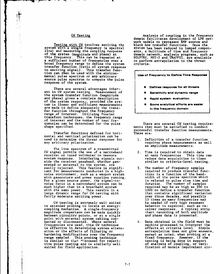
CW Testing Analysis of coupling in the frequencydomain facilitates development of LPN net-work models to represent EMP source and
Testing with CW involves exciting the black box transfer functions. Once thesystem with a single frequency (a spectral system has been reduced t9 lumped compon-line) and measuring the coupling response ents, a multitude of time and frequencyof the system (magnitude and phase) at domain network, analysis programs, such asthis frequency. This can be repeated at SCEPTRE, NET-2 and TRAFFIC, are availablea sufficient number of frequencies over a to perform extrapolation to the threatbroad frequency range to define the system criteria.transfer function (ratio of system responseto exciting signal). This transfer func-tion can then be used with the environ- -mental pulse spectrum or any arbitrary Use of Frequency to Define Time Responsesource pulse spectrum to compute the pulseresponse of the system.
There are several advantages inher-ent in CW system testing. Measurement of 0 Sensitivity and dynamic rangethe system transfer function (magnitudeand phase) gives a complete description 0 Rapid system evaluationof the system responsi, provided the sys-tem is linear and sufficient measurements * Some analytical efforts are easierare made to define adequately the trans- in the frequency domainfer function throughout the frequencyrange of interest. Utilizing Fouriertransform techniques, the frequency rangeof interest and the number of test fre-quencies can be determined for the pulse There are several CW testing require-shape specified. ments that must be satisfied to conduct
successful transfer function measurements.Transfer functions defined for hori- These are:
zontal and vertical polarization can beused to determine the threat response for 1. Definition of a transfer functionany arbitrary polarization, requires phase measurements as well
as amplitude measurements.The line spectrum of a transmitted
CW signal permits the use of a narrowband 2. Time is required to obtain datareceiver or tuned voltmeter to measure at many frequencies This time cansystem response. Interfering signals out- reduce data acquisition to timesside the receiver passband, whether gen- similar to criteria-level testing.erated or external to the system, areeasily rejected. This feature is signifi- 3. The number of frequency samplescant for measurements conducted in a high- required to produce transfer func-noise environment, such as a weapon system ticns is a function of the band-with generators and power supplies running. width of the pulse spectrum whichFor a given source power, the signal-to- is related to pulse rise time andnoise ratio in a narrowband system can be duration. The number of samplesmuch higher than in a broadband system required may be as high as 500 towith the same power. This results in a 1000 to define a transfer functionlarge dynamic range for CW testing with that contains significant variationfairly moderate exciting power. over three decades, and possibly
10 times as many frequencies mayCW testing is extremely well suited be needed if very high resonant
to extended probing to locate an energy- behavior is expected, such as re-coupling mechanism. A single-frequency ceiver responses. A typical stripmagnitude comparison can be made quickly chart recording of both amplitudebetween circuitry points, or at a single and phase data is presented.point with external system cabling con-nected or disconnected. Where several 4. Data obtained in the field must befrequencies are used, this CW technique machine processed to interpret theis effective in determining system attenu- effects at criteria level. Simpleation or the effects of filtering or extrapolation does not give answers,hardening modifications over the frequency except as noted, when probing at arange sampled. This probing technique fixed frequency. However, if theis similar to that Aiscussed for repeti- testing is being done in supporttive pulse testing and is similarly well of analysis of coupling, or veri-suited for field application. fication of models (equivalent cir-
7-7
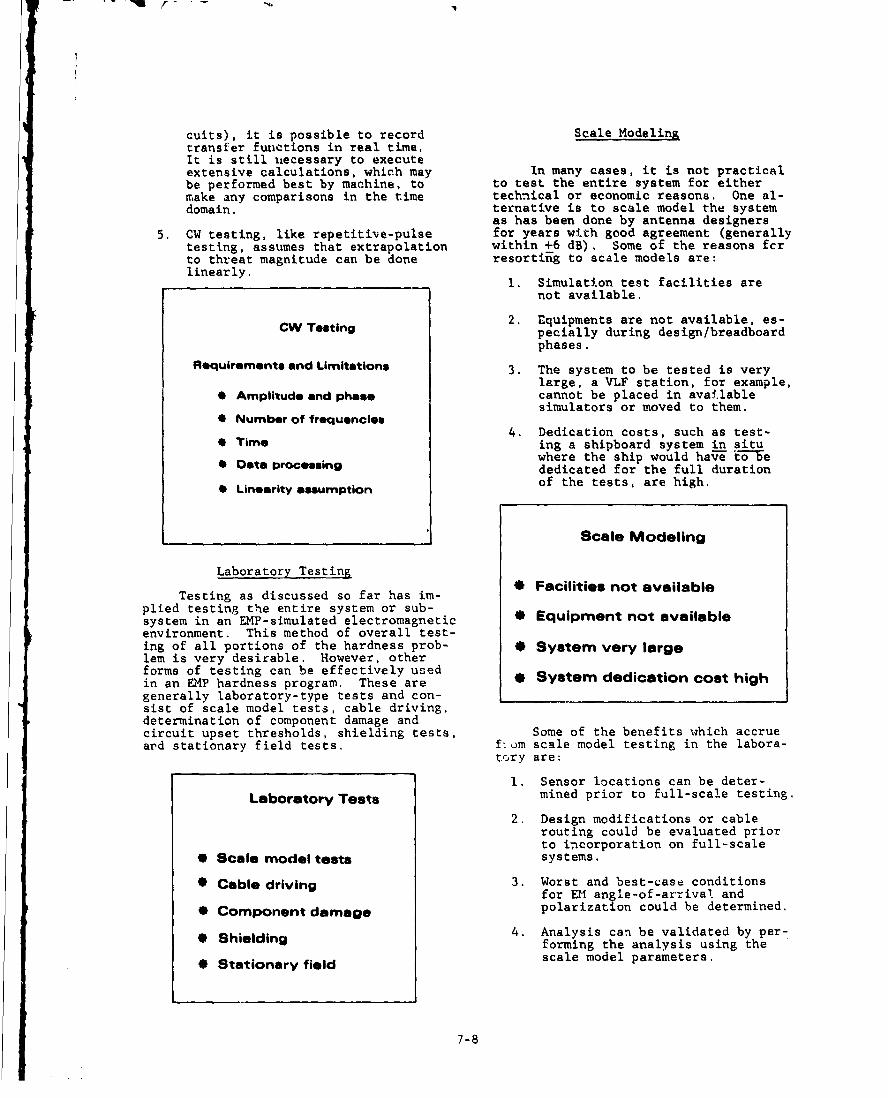
cults), it is possible to record Scale Modelingtransfer functions in real time.It is still iiecessary to executeextensive calculations, which may In many cases, it is not practicalbe performed best by machine, to to test the entire system for eithermake any comparisons in the time technical or economic reasons. One al-domain. ternative is to scale model the system
as has been done by antenna designers5. CW testing, like repetitive-pulse for years with good agreement (generally
testing, assumes that extrapolation within +6 dB). Some of the reasons fcrto threat magnitude can be done resortinig to scale models are:linearly.linearly 1. Simulation test facilities are
not available.C• Testing 2. Equipments are not available, es-
pecially during design/breadboardphases.
Requirements and Limitations 3. The system to be tested is very
large, a VLF station, for example,0 Amplitude and phase cannot be placed in available
simulators or moved to them.* Number of frequencies
4. Dedication costs, such as test-* Time ing a shipboard system in situ
where the ship would have 5to e0 Date processing dedicated for the full duration
• Linearity assumption of the tests, are high.
Scale Modeling
Laboratory Testing * Facilities not availableTesting as discussed so far has im-
plied testing the entire system or sub-system in an EMP-simulated electromagnetic * Equipment not availableenvironment. This method of overall test-ing of all portions of the hardness prob- 0 System very largelem is very desirable. However, otherforms of testing can be effectively usedin an EMP hardness program. These aregenerally laboratory-type tests and con-sist of scale model tests, cable driving,determination of component damage andcircuit upset thresholds, shielding tests, Some of the benefits which accrueard stationary field tests. fiom scale model testing in the labora-
tory are:
1. Sensor locations can be deter-Laboratory Tests mined prior to full-scale testing.
2. Design modifications or cablerouting could be evaluated priorto iicorporation on full-scale
0 Scale model tests systems.
* Cable driving 3. Worst and best-case conditionsfor EM angle-of-arrival and
0 Component damage polarization could be determined.
* Shielding 4. Analysis can be validated by per-forming the analysis using the
* Stationary field scale model parameters.
7-8

'it must be recognized that, because Direct Injection Testingof the difficulty in introducing minuteopenings or poor bonds into models, andsince these often control interior fields, Current and/or voltage waveformsthe usefulness of modeling is ordinarily can be directly injected into the systemlimited to the measurement of external cables or equipment terminals to deter-fields, voltages, and currents. mine upset/damage levels or the transfer
function response of the system. Thesystem configuration and test objectives
ADVANTAGES: will determine the required characteris-tics of the driving source.
* LOW COSTSub-criteria level and low level
* CONFIRM4 DESIGN coupling tests can be combined with* VALIDATE ANALYSIS criteria level inlection tests to evalu-
ate system degradation effects. These0 DETERMINE WORST CASE THREAT tests involve injecting the waveforms
* AID IN SENSOR PLACEMENT monitored during low level field testswith amplitudes scaled to criteria levels.
* EVALUATE DESIGN MODIFICATIONS It is very difficult and costly to gen-erate the complex waveforms often ob-
DISADVANTAGES: served, especially at the criteria levels,An alternative, mentioned previously, is
"* EXTERNAL FIELDS, CURRENTS, to generate a series of discrete frequencyVnLTAGES ONLY waveforms one at a time which cover the
"* ALL EFFECTS NOT INCLUDED frequency spectra of the measured wave-forms. To select the proper frequenciesand waveform amplitudes usually requirescareful analysis.
Transfer function measurements canIn general, the same test techniques be performed using either CW or pulse
as for full-scale tests apply to scaled type sources. Pulse sources must havemodels. The test sources and illuminators a frequency spectrum consistent with theas well as the scale model of the systems anticipated or measured spectrum of themust satisfy certain general relationships. energy coupled to the system. CW sources,These relationships are shown in the fol- being discrete spectral line sources,lowing figure. One important considera- must be available over the same spectrum.tion in the scale model is that it is not These pulse and CW sources are usuallyalways feasible to scale conductivity of much less costly than coupling sourcesthe enclosure. In order to reduce losses, because this technique uses a small sourcesince the frequency is scaled up, one al- tightly coupled to one port rather thanternative is to scale the conductivity/ a large source loosely coupled to thewall-thickness product (usts a t a). entire system.
Direct injection testing has the ad-vantage that one or more ports can be
GENERAL RELATIONSHIPS studied singularly or in any combination.It is particularly useful when components
MDa or circuits must be subjected to transientMODEL SIZE D5 - voltages or currents to determine their
H damage thresholds and failure points.
FREQUENCY ws Mw a The main disadvantage associatedwith direct injection testing is that the
CONDUCTIVITY Mu actual free field coupling to the total
system cannot be simulated. CorrectlyPERMITTIVITY s a phasing 'and shaping the pulses for a
multiport injection system can be veryPERMEABILITY aJs • difficult. Also, depending on the point
wAVELiNGTH -- of injection, any nonlinear effects may5 or may not be resolved.
PROPAGATION LOSS a MS a Component Damage Testing
PROPAGATION PHASE *s Mp a Components or circuits, both opera-tional or in the breadboard stages, canbe subjected to large voltages and cur-rents to determine their damage or upsetthresholds. The components which should
7-9

be subjected to damage testing are those waveform or simulation thereof is em-that normolly would terminate long cable ployed.runs or antenna input cables. When low level coupling is employed,
Component damage teat3 provide a data analysis provides for interpretation ofbase for use in predicting potential prob- the measured coupling transfer functionlem areas for both existing systems and in terms of the EMP environment criteria,thoso in the design stages. The data base Further, analysis must be employed to re-is valuable as an ald in selecting com- late the laboratory tests on individualponents for use in new systems, equipments to the environment criteria.
These levels can then be compared andBased on component failure or circuit the potential for damage or upset assessed.
upset level, the amount of protection re-quired to harden the system can also be Analysis can also be employed tospecified for the postulated threat, predict the coupling response of the sys-
tem (see Section IV). The laboratorytests and additional analysis can then beemployed as in the case of low levelcoupling testing.
Component Damage and Circuit upset Tests 7.3 TRANSIENT ENERGY SOURCES
Transient energy sources used in EMP* Establish data base hardness testing vary in complexity from
simple commercial laboratory pulse gener-* Aid incomponentselection ators used for component testing to sophis-
ticated multimegavolt systems used inI Establish protection requirements large scale simulators for complete sys-
tems tests. Standard commercially avail-able pulse sources will be discussedbriefly to aid the user in establishinga test setup.
Shielding TestsAn introduction to the various gen-
eric types of energy sources includingShieldiag tests are most often per- the storage elements, switching arrange-
formed at the subsystem level. Such test- ments, and the power supplies is provided.ing can verify construction design and can This diszussion will be slanted towardlocate ene.rgy penetration points before considerations of the test facility usercoilstruction is complete. rather than the designer.
Measurement of the shielding effect-iveness of a facility or enclosure when Energy Sources for Component and Circuitconstructed can also be used for hardness Testingsurveillance over the system life cycle.Periodic measurement of the shielding Component and circuit testing gener-effectiveness will evaluate the condition ally involves direct injection of currentof the shield by noting changes (deterio- at the component or circuit terminals.ration) with time. The purpose of these tests is usually to
determine upset or damage thresholds. Assuch, only low voltage/current pulse
Analysis sources are required.
Analysis must be used in combination There are a wide variety of pulsewith any of the test concepts. At -iter- sources available commercially with volt-ia-level, testing analysis provides ror age ranges from a few volts to a fewextending the test results to other en- hundred volts, (such as the Velonex Pulsevironments, system configurations, and lenerator) and current ranges from milli-system operating modes. amps to several amps. These units pro-
vide for variable output voltage, rise1're-test analysis is useful for de- times, pulse widths, and fall times in
termining expected signal levels at criti- many cases. These units are adequate forcal EMP entry points, most component and circuit testing.
When sub-criteria level testing is If greater power is required, theseemployed to determine coupling, analysis units may be used in conjunction withis required to scale the measured volt- wide band (0-220 MHz) power amplifiersages and currents to criteria levels for to faithfully amplify the pulse and pre-direct iiJection testing where the correct serve the rise time, These higher power
7-10

units are usually available with select- lent inductance of the capacitor and itsable output impedances for matching pur- connecting wiring or it may be a deliber-poses and current limiting provisions so ately added inductance chosen to obtainthe amplifier will not be damaged by fail- a desired pulse rise time.ure tests where the failure may be mani-fest as a short circuit. Typical ampli-fiers which are available have 100 wattCW/400 watt pulse and 1 Kw CW/4Kw pulsecapability. L t=O
High-Level Energy Sources - Basic Energy E
The basic elements of an energy sourcefor use with an EMP simulator or directinjection pulser are contained in a capac-itive disc harge pulser as illustrated.
The load impedance is shown to beresistive which results in an exponentialdecay of a sinusoidal load voltage. Thestorage capacitance and load inductance
Charging determine the sinusoid frequency, and theReasitor Spark Gap resistance determines the envelope decay0 -0•--4- time constant or Q of the tuned circuit'.
High 8oeCapacitor To Load Another approach to obtain an energy
Supply lsource is to use a coaxial cable for theT =storage element. When the spark gapfires, the charged line voltage is dividedbetween the line impedance and load im-pedance. The voltage wave travels downthe line and is reflected by the chargingresistor which is usually high compared
___to the line impedance. The reflected!iave then returns down the line. If the
The source consists of a high volt- load impedance equals the line impedarce,age power supply, a storage element (caoac- then a voltage step of 1/2 the line charg-itor), a current limiting charge resistor, ing voltage is applied to the load for aand a switch for connecting the storage time equal to twice the line length. Noteelement to the load which can be a radiat- that the coaxial line storage element re-ing structure, a bounded wave structure or quires twice the charging voltage of anthe terminals of a subsystem under test. equivalent capacitor storage energy source.The decay time of the load voltage is de-termined by the storage capacitance valueand the load impedance (resistance). Therise time of the applied voltage is con-trolled by the spark gap characteristics.Thus, the load, if resistive, will see atransient with a rapid exponential riseand a longer exponential decay. The char,-ing rate is controlled by the storage Charging Spark Gapcopacitance, charging resistor, and current Resistorcapability of the power supply. Normally, N.1h Storagethe storage capacitance is selected to Voh Lgive the desired transient decay time, and voltag L,,•e Ta Loadthe charging resistor is selected for the supplydesired pulse repetition rate.
The capacitor discharge pulser canbe represented by the simple RLC circuitshown. The storage capacitor C is chargedto an initial voltage Vo and the switchis closed at t - 0 to discharge the capac-itor into the load shown as a rbsestor R.The series inductance L may be the equ.va-
7-11

The pulse shapes and their spectral Noninductive cnpacitance at highcontent differ for the two types of stor- voltages is difficult to obtain, Theage elements. The ideal charged trans- addition of an inductance to form an RLCmission line matched to the load produces network can be used to modify the coaxiala rectangular pulse of width T, while the line transient shape as shown here. Thelumped-capacitance source produced an ax- notch, expaudel in the righthand waveform,ponentially decaying pulse of the time Is caused by the finite rise time restric-constant T. The rectangular pulse from tion in the LC circuit. This notch can bethe transmission line has zeros at fre- smeared by using more than one coaxialuencies determined by the pulse width line and using slightly differcnt line1/2T), whereas the exponential pulse lengths.
from the lumped-capacitance source con-taint no finite zeros in its spectrum.Because a real transmission line does notproduce a perfectly rectangular pulse, c, 4a-fthe zeros of the ideal pulse spectrumwill become minimal in a real pulse spec-Ltrum. Nevertheless, if a criticai cir- fccuit or element is resonant at one of the Tnull frequencies, it may not be excitedsufficiently to produce the desired re-sponse one should acquire for the test.
t The charged transmission line canbe used to produce a damped oscillatorywaveform if the line is open circuited atone end (Rs >> Lo) and its characteristicimpedance is greater than the load im-pedance (RL < Zo). As illustrated, thewaveform begins as a square wave oscil-lation and decays into approximately a* ZTf sinusoidal wave after propagating a fewround trips on the line.
The square pulse that is inherentin the coaxial line storage systen can -- $Zo C V(Otbe modified to improve the spectral[ }CZZ 70content. With negligitle inductance in _ _
the circuit, the storage capacitor en-ergy dumped into the coaxial line pro-duces a square pulse as Is shown here.The resistance Z_ in series with C RLVQ --prevents the capacitor from presenting R+÷Zothe line with a high-frequency short ^t-that would cause an additional tran- |0sient at four times the line length.
V V V V
Chorged Line For A Damped oscillatory Waveform
C I Marx Generator
Generators are readily availablewhich will produce voltages up to the ten'sof kilo iolts range. Larger voltages kmega-volts) are obtainable by using specialcapacitor charging schemes. In a Marxgenerator, a bank of capacitors is chargedin parallel. When the switches are closed,
7-12

the capacitors are discharged in series, triggering erection scheme is iilustratedThe series multiple gaps Ptnd their in- trated below (the dc charging circuitsductances limit the discharge rise time have been left off to emphasize the tran-as discussed earlier, sient circuit).
Marx generator design has been im- Zý"-utpt Outputproved so that these generators can be Ioperated to produce waveforms with nano- Iaecond rise times. The principle of oper- -ation of the Marx generator can be seenfrom the circuit diagram illustrated.
Each capacitor in the capacitor ,stack is charged to the dc power supply ,voltage (Vo) through the resistors along-side the capacitor stack. To erect theMarx generator, the switch at the bottom Iof the stack is closed to connect thebottom two capacitors in series, causingthe voltage across the next switch to in- I..crease momentarily to well above its Tr ,-W'- ThiprIn Ibreakdown threshold. The second switchthus closes and overvoltages the third"-switch, and so on unt!.l all the switchesare closed and the capacitors are connected MARX GENERATOR SELF-TRIGGERING ERECTION SCHEMESin series. Thus, for N stages of capac-itors charged to an initial voltage. Vo,theoretically a peak voltage of NVo canbe obtained.
LC Inversion Generator
An alternate method of voltage en-hancement is an LC inversion generator.Pere, two charging capacitors are chargedwith opposing polarities. When the in-version switch is closed, the voltage on
4 the lower capacitor will vary sinusoidallyat a frequency determined by the LC cir-
6V0 cuit. When this voltage has reversedpolarity, the voltage at the output istwice the charging voltage. Multiplesections of this generator can be placedin series to fire a single gap to the load.The ringing effect in the LC inversiongenerator is undesirable for some appli-cations.
SDC.
Basic Marx Generator Circuit Diagram-- output L# --k
The time required to discharge such ,v. V2%
a generator is dependent on the stacklength (number of stages), ionizationtimes, gap inductance and load impedance • , .,t, kni.t4
of the gaps, etc. For megavolt rangepulsers, rise times on the order of micro- 26-seconds are typical. -.
Fast erection of the stack is ob- 4wVw , etained by triggering the spark gap switchesand xeducing the size and inductance of vo.gv.. ,Tmm.ethe stack by developing high energy den-sity capacitors and special packagingconcepts. A typical Marx generator self-
7-13

Van de Graaff Generator
Another high voltage supply which hasbeen used is the Van de Graaff generator.Supplies of this type are capable of gen- S1 S2erating extremely high voltages. General- 0ly, since these generators utilize staticcharge transfer, the charging time is quite Lmlong. Supplies of this type find their RLmain usage in criteria-level simulation of Cmthe single-shot type since charging times Cmare too long to bj utilized in a repetitivepulse type simulator where several pulses T Tper second are desired. Storage Peaking Load
Capacitor Capacitor
If Vo is the peak voltage of the highvoltage generator, the peak current inthe load (for a zero rise time pulse) is
- Vo/RL. The value of - is chosen so that,d= -when the voltage acrosA it reaches Vo,
after switch S 4*s clused, the currentthrough it is V /RL, At this time, switchS2 is closed ana the voltage across, andthe current through the load immediatelybecome Vo and V /RL, respectively. Be-cause the capacytance C RL, and theinterconnecting conductbrs contain someinductance, the rise times oi the voltageare greater than zero in practice; hcw-ever, for the purpose of illustrating theprinciples employed, this stray inductance
Peaking and Transfer Capacitors was neglected.
The advantage of the peaking capac-High-voltage generators that produce itance method is that it permits a fairly
voltages in the megavolt range are physic- small. high-quality (low inductance) capac-ally large and usually contain too much itance to be used to form the leading edgeinductance to deliver wavefcrmns in the 1 of the pulse, with the primary energyto 10 ns range directly to the load. Con- storage remaining in the high-voltage gen-seouently, some means of reducing the rise erator.time of the pulse delivered to the leadmust be incorporated into the high voltage, The circuit for a transfer capacitorfast rise time machines. The schemes is identical to that for a peaking capac-commonly used for reducing the rise time itor. The difference between the two isof the waveform delivered to the load in- that only a portion of the source energycorporate transfer or peaking capacitors is temporarily stored in a peaking capac-at the output of the generators. itor, while all of the source ernergy is
temporarily stored in a tran.fer capacitorThe peaking capacitor is a low value The transfer capacitor must be a low in-
(compared to the erected stack capaci- duct-nce device if fast rise times are totance), high-voltage, low-inductance ca- be achieved. Because the energy is onlypacitor that is capable of storing enough stored temporarily, however, leaky high-energy from the generator to allow the energy density dielectrics, such as water,current to build up to the level required can be used to make compact, low induc-by the load. When the generator current tance transfer capacitors.has built up, the load is connected andthe current is transferred to the load, Transfer capacitors are used primar-
ily in short-pulse systems in which theThe peaking capacitor circuit is total stored energy is relatively small.
shown schematically, where Cm and Lm are Their advantage, compared to pzaking capac-the capacitance of the capacitor bank in itors, is that they can be used with loadthe high voltage generator, C is the peak- impedances that are neither constant, re-ing capacitor and RL is the 1had resistance. sistive, nor necessarIly well defined.
7.14

Switches
The switch inductance is the final Loserlimiting factor on rise time. The switch Beomdesign is quite complex. A simple gap inair will fire when the voltage gradientreaches 20 kV/m at 1 atmosphere pressure.This arc will have a length and currantthat determine its inductance. The arclength (electrcde spacing) can be reduced Lensby pressurizing the switch and properselection of the gas or gas mixture.
Axial LaserTrigger
looc.
S F,
E CW Energy Sources1010 Air
S.. O The elements of a CW energy source
to are shown here. CW frequencies are se-lectt:d from a stable source, amplified,in this case by a broadband amplifier,and matched to the radiating element.
o0 2 3 4 An alt :nate method is to use a tunedamplifier as the power amplifier. Gener-
Pmas*ure-Atmoaphares alMy, commercial equipment is availablefor CW energies.
cw T-,.s t,-
Spark-gap switches are often triggeredto control the firing time. Two techniques , ....are used. A laser can be used to produceionization in the gap, or a pulse can be L. _ ............ Aapplied to a third electrode in the gapto initiate breakdown. This latter meth-od adds additional circuitry into theactive part of the system that must be in- L ... 7-cluded in the pulser design. -... _....
TriggerElectrode
7.4 ELECTROMAGNETIC PUiSE FIELDSULATION
The EMP environment is usually de-fined as an electromagnetic plane wavepropagating in free space. While it isnot possible to exactly duplicate thisenvironment, illuminating structures canbe built which provide a good simulationof the environment over a large enoughvolume to obtain a valid assessment of a
MID-PLANE TRIGGER system.
Thero are two basic types of simu-lators commonly encountered in EMP test-ing. These two types are bounded wave ortransmission line structures, and radiating
7-15

antenna (mono pole or dipole) structures.Other types of simulators are usuallyvariations of these two basic types.
Compo.Ints of a Transmission Line Simulator
Bounded Wave Simulator-- Flat Conducting
Surfaces
One efficient, broad bandwidth illum- Energy Working Termination
inator that is commonly used and is simple Source Voi,. ,eto construct is a transmission line simu-lator. This illuminator is a sounded-wave TransitionJstructure that is based upon a strip-line Sectionstransmission line.
The principle of operation of atransmission line EMP simulator is toguide an electromagnetic wave across atest object situated between the two me-tallic surfaces of a transmission line.The essential elements of this simula- Let us consider some of the charac-tor include an energy source, transition teristics of transmission line simulatorssections, a working volume, and a termi- by an example. Shown is a transmissionnation. An electromagnetic wave is gen- line with a 15 m x 24 m x 12 m high work-eratad by the pulse being applied to the ing volume. The line is over a flattransmrissicn line and allowed to propa- ground plane and has transition sectionsgate i_. the terminal end. To provide that are 50 m long.the connection to the pulser and termi-nation, transition sections of constant The impedance of the transmissionimpedance are utilized. The cross-sec- line is a function of the width-tc-heighttional dimensions of the working volume ratio which is constant from source to(i.e., the separation and plate width termination.of the parallel metallic surfaces) mustbe large enough to provide a specifieddegree of field uniformity over the tes t
object. A termination is provided to TOPprevent the reflection of the guided 1_wave back into the working volume. Thi2termination is generally achieved bymeans of a transition section that guides -50- _15 _-the wave to a geometrically small re-sistive load whose impedance is equalto the characteristic impedance of thetransmission line structure. Thus, for SIDE ,12a transmission line simulator, most ofthe available energy is confined or .bound to the space within the line so EARTHthat large-magnitude fields are easilyattainable. I
Bounded wave (transmission line)simulators are generally capable of gen- For an upper plate wid.h of 2a at aerating EM fields at the EMP specifica- height h above a perfect ground plane,tion criteria level. The wave imledance the line impedance varies from 180 ohmsin Lnfe simulator is that of free sDace for a/h = 0.2 co 40 ohms for a/h = 3.5.(377 Q). Their principle application For our example, if the ground plane isis for missiles and aircraft in flight a perfect conductor and the working vol-sirce ground effects are not present in ume has a ratio of a/h = 1, the impedancethese simulators. Also, they have lir:ited of the line would be 89 ohms.interaction volumes, Droduce only a singlepolarization (normally vertical), and This impedance is for infinite widthsingli angle of arrival. Different of the perfect ground plane.nolarizaticns -id angles of arrival arcachieved by rotating the system undertest which again places a restrictionon system size that can be ccnvenieutlyhandled.
7-16

-_hi_
I S O . OL 12 2 3 --
1200012
o 100 I : 0
N00 10
so- 100-N 905 I I
o I 2 3 4 80 1
As the width of the lower plate is The electromagnetic field orienta-decreased, the line impedance will in- tion and relative magnitudes for a strip-crease. Shown is an impedance parameter, line transmission line can be displayedZ', that is proportional to line impedance, by a plot of equipotential lines and fieldZ, and upper plate width-to-height ratio, lines. The equipotential lines show thea/h. As the width of the lower plate d magnetic field orientation, and theiris decreased for any a/h ratio, Z' shows spacing relates to the electric field mag-an increase. nitude (volts per meter). The field lines
on the plot show the electric field orien-tation, and their spacing relates to themagnetic field magnitude (amps per meter).
Z' Versus -1 with A as a parameter The electric and magnetic fields are re-lated by the wave impedance which is the""1 free-space impedance of 1207 or 377 onms.
- For our example where a/h = 1 (Z = 178 ohmi2. - .. -2h)which is not the wave impedance), the
h2o• '7.' field is essentially uniform under most, . .d of the volume covered by the upper plate.
z. d.. , -- . . - ,d
0 •25 ,,,/ , 2.50 Field and Potential Distribution for Parallel,45 1 .00 Two-plate Transmission Line, 178.18 Ohms
0.50 . , ,
35 a/h 1.00
2 4 2. 4 6 10
For our example with a/h = 1, as the
width of the lower plate (w) is reduced .. A-to the width of the upper plate (w/a = 1),the line impedance will increase from 89 .:j•"-i;-"'•ohms to 116 ohms. If we were to construct _ _.----.
our example line with lower plate width ........ _____-___-___
twice the upper plate width (w/a = 2),then the line impedance would be 97 ohms.However, since the earth, which is a con-ductor, extends beyond the low;er platewidth, the actual impedance would be less The field uniformity is dependentthan the indicated 97 ohms. For the upon the plate width-to-height ratio aspresence of a real earth to have negligi- indicated here for two extreme a/h ratios.ble effect, the lower plate should be four For a/h ratios greater than one, the uni-times the width of the upper plate. formity of the field is improved. For
7-17

the 360-ohm line shown, a/h - 0.2, the The fields wihin the working volumeelectric field magnitude just below the have been defined, These fields areupper plate is about 2.8 times the field essentially a TEM mode. For frequenciesdirectly below at the lower plate. higher than the frequency at which the
plate spacing, h, is half wavelength, itis possible to maintain higher order
-M.TIwLi.,,.,7Ot- modes. However, since the wave is launchedS Iat a narrow plate spacing at the beginningIi -of the transition section, only the low-
est order transverse mode is launched.This mode travels down the transmissionline and is not altered unless some dis-continuity converts energy to the higher-order modes.
The magnitude of the field is a func-tion of the applied voltage, Vo, andplate spacing, h. Thus, in the working
Pd d •tW ... volume the electric field is Vo/h v/m.W-pftfctT., o Lino.. 300.0, Oho The magnetic field is Vo/hro, where no isW..o the free-space impedance (377 ohms).
Within the source transition the electricfield is Vo 1 /ht, where Z1 is the lengthof the transition and Z is the distancefrom the source. The fields in the term-ination transition are similar. The max-imumn fields are generated at the sourceand termination.
Source Termination
As a/h is reduced below unity, the I la Ifields at the top center and bottom edgeof the working volume relative to thefield at the bottom center vary as Lhown.
The field distortion is greater atthe top center of the working volume thanat the lower edge. This is indicated bythe dashed lines which show the 20% .,ari-ation points. For a maximum of 20% change Ein field magnitude at the top, a/h mustbe greater than 0.7, while the same dis-tortion limit at the edge can be met for 2 h Voa/h = 0.4. ____ -h-
Distance -
The wavefront in the transition sec-TOp tion is spherical as shown. When this
Reference Edge wave intercepts the working volume, re-flections occur that: will cause the field
at B to be distorted. Fields at A should"- AtTop be a reproduction of tCe source signal.
Uniform Field
I At EdgeI I
iL _ It I I 1 -111
0 L 0.4 os 2 L
A
7-18

The accompanying figure shows two One method to achieve a more planarmeasured waveforms for a step input to wavefront is the use of multiple tran-the Alecs transmission line. A is the sition sectious as indicated here.undistorted waveform. At B the reflected(and delayed) wave causes a distortionof the rise of the wave and alters themaximum amplitude.
A Z Z
It is desirable that the field in the For the same length transition sec-working volume be a plane wave as indicated tion, the spherical tilt is reduced. Thisby the dashed line. However, the wave improvement occurs even when the transi-from the transition section is spherical tion angle, e, is held constant as indi-which means that the time of arrival of cated.the wavefront at the top and bottom sur-faces differs by At. The wave appears Multiple feeds force the spherical"tilted." For our example line with a and plane wavefronts to be identical atheight of 12 meters and a transition length the edges of the transition sections.of 50 meters, the time At is 5 nsec.
The wave tilt (At) is a measure ofthe time involved in going from the spher-ical wave to a plane wave in the workingvolume and is representative of the risetime of the line. A similar distortionoccurs when the spherical wave interceptsthe discontinuity at the beginning of theworking volume at the edges of the upperplate.
The distoition at the mating of thetransition section and working volume canbe reduced by increasing the length of thetransition section.
So f .r we have discussed a trans-r Working mission liie that is made of solid con-
Volume ducting plates. Portions of the line canbe replaced with parallel wires if the
Transition spacing between wires is small comparedto the highest-frequency wavelength. Thisuse of spaced wires causes the field with-
-- At - in a wire spacing to be distorted and willincrease the line impedance. The effectof the parallel wires can be consideredas an increase (Ah) in the vertical spac-ing between solid plates. For example, ifthe upper T te of our example line were
7-19

made of #14 wire on 0.3 meter spacings Horimontally-Polarized Simulator(0.1 X at 100 MHz), the increase in ef-fective plate spacing would be 0.2 meter.For the 12-meter plate spacing in the ex-ample, the effect on the impedance would ____
be sniall. For small transmission linea0 -2- 0610 "the effect can be appreciable. " 0icttS.ri _
th -k .. q V , PS V;OW
' IAh -ýI d Pulro nptAý_
Q Q The field distribution within a hor-
RadiusI. izontal transmission line is altered bythe presence of the ground boundary onone side of the line. Shown are the equi-potential lines with and without the
Grid Extends with - presence of a perfect grou.id plane. TheRepetitive Spacing presence of the ground greatly alters the
to Both Sides field orientation.
F~eld stlb~ltlo W.01 Ind Whout G, ,td Ple
For transmission lines made of paral- / .lel wires as shown, the plates are not"perfect conducting plates, and at thehigher frequencies will radiate energy. ' I "This radiation will cause a loss of high-frequency content in the wave and will I, / /maintain a spherical wavefront for high _frequencies within the working volume. ' ,The transmission line car. be crudelylikened to a vertical rhombic antenna. __,__,
The length of the line does not affect W,,•....•G..dPI.-
radiation from the line as long as the ----.. w,,ro,,,' .... d P....
length is long compared to the height.However, as X/4 approaches the plate spac-ing, the line will start to radiate as avertical rhombic. For our example, a This orientation can be improved byline with a plate spacing of 1.2 meters, the use of wires to alter the field dis-frequencies above about 6 MHz will radi- tribution. Shown is the effect of twoate, affecting high frequencies in the wires at one-half plate potential. Moreline. complex configurations can make addition-
al improvements.Transmission lines can also be used
to create horizontal electric fields byerecting the plates vertically. Shownhere is a concept that permits easy accessto the work area. The work area is at A Field Distribution with Auxiliary conductors
the end of the source transition. Theline termination is approximated by allow-ing the transmission line impedance toincrease toward the free-space impedance3"of 377 Q2. v* V0 ,' _'
7 -2
7-20

So far we have discussed the fields The field distrubance due to thewithin a bounded structure (transmission cylinder for various d/h ratios is shownline) without any conducting material here. The maximum disturbance occurs at(equipment) in the line. If the line di- A. The fields at B near the cylinder aremensions are large compared to the equip- less altered. This enhancement of thement dimensions, then the field distortions field between the cylinder and platescaused by the equipment will have little effectively increases the transmissioneffect on the fields created by the line, line capacitance and thus alters the lineHowever, as is more often the case, the impedance. For a line with a d/h - 0.6transmission line is made just big enough cylinder, the incremental line admittanceto contain the maximum dimension of the is altered by 20%.equipment being tested.
Placing a test object in the working ---
volume can reflect and distort the inci-dent wave. Large reflections directedback into the pulser might be objectionable 4if they either exceed the reverse voltagerating of the pulser or're-reflect from E
the pulser back into the working volume. EO A
There will also be a certain amountof distortion in the vicinity of a metal- CClic test object illuminated by a radiatedplane wave. Providing the differences infield distortion between radiated plane C0 02 04 06 GB 1.0
wave illumination and a wave guided by atransmission line simulator whose cross-sectional dimensions are not significant-ly different from that of the test object The effect upon the signal inducedare small, the use of the transmission in a conductor can be approximated asline simulator is acceptable. shown. If a missile, approximated by a
cylinder of diameter b and length d, isA conductor in a transmission line positioned between the plates of a trans-
will alter the field structure in the line. mission line as shown, an infinite seriesShown is a transmission line with an in- of images results, For d approaching h,finite cylinder that is 0.6h in diameter the effect is to load the line, reducing(d/h - 0.6). The equipotential lines can the field in the vicinity of the cylinder.be seen to bunch between the cylinder andplates and are spread either side of thecylinder. The field at the upper plate(A in the figure) is enhanced to 2.28times the undisturbed field in the line.At points B and C the field is 0.74 and0.99 the undisturbed field, respectively.
Plate
_T atdT"C Inc
E, -~ hb Is Equivalent To z
2128A
This loading reduces the peakcurrent at the center of the cylinderas shown here. The reduction is lessthan 10% for d/h ratios less than 0.6.
7-21

-0 w qa -83
S~Ho
hLdO A ionc A"~ Roof a
AS
D 0 2 0 14 0 6 1 t 0 3 ..10-&-C Ho
The effect of a large object in a Pulsed Radiated Wave Simulatortransmission line can be illustrated bythe example shown here. Modeled is atransmission line constructed over a An alternate method of subjecting alarge rectangular building of height b. test object or system to a simulated EMPThe transmission line width is the width field is to use a radiating structure orof the building, and the building length antenna. A radiated-wave simulator radi-fills the working volume. Shown are the ates a free field which is not confinedrelative magnetic fields for a step in- within the boundaries of the simulatorput to the line. For a building-to-line structure.height ratio b/h - 0.83, the field at thefront face and over the building is en- An EMP-radiating simulator has sev-hanced with high frequencies, while the eral relative advantages. One is thathigh frequencies are attenuated at the construction is usually simpler andback face. For a b/h ratio of 0.57 all costs are usually less than those assoc-fields are a fairly good reproduction of iated with a transmission line simulator.the incident step function. Another important advar.tage of a radiat-
ing simulator is that the space availableThese results can be explained using to place test objects is not limited by
a transition section mismatched into a the structure's dimensions. The dis-relatively low-impedance line formed by advantage of such a simulator is thatthe upper plate and building roof. The only a fraction of the stored energy isresulting reflections give voltages on directed to the test object due to thethe line that result in the measured relatively nondirectional radiationfields, patterns of antennas used on existing
simulators. Furthermore, there is ageometrical I/R attenuation of the radi-ated wave amplitude with distance from
,o the source. This geometrical attenua-I tion causes a difficult tradeoff betweenI high field intensities that can be
achieved close to the antenna versus thenearly planar field distribution overlarge areas that can be obtained further
-Fo.83 away fiom the antenna.± . .Pulse radiating simulators are gen-
erally of the biconic dipole or invertedconical monopble design. The dipole sim-ulators are of the order of 1000 feet ormore in length. Like the long-wiresimulators, planarity over larger workingvolumes is obtained at the expense offield level (h/R falloff). The availablepolarization from the dipole facilitiesis predominantly horizontal on the line
The peak magnetic field over the normal to the dipole axis and throughbuilding indicates that, for b/h ratios the feed point of the biconic. Angle ofless than 0.6, the transmission line can arrival is also variable by varying theproduce relatively uniform fields. distance from the simulator. Ground
7-22

effects must be considered. The clear This feature can be overcome by thetime (time before arrival of the reflected use of a biconic dipole shown here. Thepulse) is a function 7f distance from the biconic dipole has two cone elemetits withantenna, decreasing as the distance in- a cone angLe eoocreases. These facilities are applicableto ground based systems ranging fromAmall vehicles to building size structuresand ships. Aircraft can be tested in afly-by mode. =e lee
0The inverted conical monopole simu-
lators are usually of the order of 100 6feet high. Polarization is vertical andangle of arrival is fixed at grazing. Aswith all radiating simulators, planarityis obtained at a sacrifice of field level.Large working volumes can be obtained atreduced field levels. Ground effects area loss of the high frequency content withdistance from the simulator. These simu-lators are used where vertical fieldcoupling is of interest.
Biconic Antenna
The basic radiating antenna is a di- The biconic antenna impedance is a
pole. Shown is a cylindrical electric function of e0 and does not vary with x.
dipole of infinite length. The radiated Typically, a 14o biconic has an impedancefield is zero in the axial direction (x) of 250 n, decreasing to 50 Q at e0 - 670.
and a maximum normal to the gap. The This constant impedance with distancemagnitude of the radiated field varies as along the biconic results in an antenna
sin e. current that is only dependent upon theapplied voltage.
The radiated field time history de-pends on the current in the dipole ele- The fields emitted from a biconicments. For a step voltage applied at the (or dipole) have electric field compon-
gap, the antenna current will be a con- ents that vary as 1/R, l/R 2 . and I/R 3 .
stant voltage divided by the antenna The I/R fields are the radiated fieldsimpedance. This impedance increases log- that are a direct function of antenna
arithmically with the axial distance (x), current.causing the antenna current to decrease.The resulting radiated field for a stepvoltage applied to the antenna is a stepfollowed by a logarithmic decay. For anapplied voltage with a finite rise time,the increasing antenna impedance with x nowill degrade the radiated rise time.
X 1fI
1 Ii
Oo i!
Vt Infinitesimal Gap
Z i 120 In. 2Xr0
7-23

The radiated electric field from a The lenith of the antenna must bebiconic is E0 (t) - 6C V(t - .•)/Za R sin 0. long compared with the applied voltageFor 6 - 900 normal to the biconic), the duration so that reflections at theradiated electric field varies as shown. antenna end occur after the initial pulseThe radiated magnetic field is related to duration. Thus, the radiated signal forthe electric field (Ee) by the free-space a biconic-cylindrtcal antenna combinationimpedance (EO - nHo). Thi3 radiated field can duplicate the applied rise time andpropagates from the biconic on a spherical peak magnitude on the biconic section,wavefront. If the biconic antenna is .ong followed by a radiated 3ignal that de-compared to the applied voltape rise tme, pends upon the applied voltage and cylin-then the rise time and peak magnitude are drical antenna impedance. When thispreserved in the radi..ed field. signal. is reflected from the antenna ends,
it wiil be reradiated from the cylindricalThe near-field compon,-nts h/R2 and antenna, The reflected signal will follow
h/R 3 must be consid red near the biconLc the initial radiated pulse; i.e., if X/cor dipole. The l/R2 compcnent varies as is larger than the applied signal duration,the time integral of antenna current 3nd then the reflecte' signal will be timegradually is about 207 of the h/R cowpon- separable from the initial signal.ents. The I/R3 component is even smaller.However, at distances close to the antenna, Reflections at the dipole ends canthe magnitudes of the near-field compon- be eliminated by loading the cylindricalents should be determined so that their section of the antenna. This loading,contributions to the test object response which can be continuously distributed orcan be assessed, distributed as lumped resistors, dissi-
pates the applied signal before the an-For applied voltages with long time tenna enda. An alternate technique often
durations, a biconic dipole soon becomes employed is to terminate the antenna withvery large in diameter. Thus, biconic resistive elements to ground. This ap.-dipoles are normally used for only the proach is valid since the propý'gation ofrise time of a simulated EMP, thus limit- the low freouencies on a dipole near theing the length (x) of the uiconic section, earth can be treated as a transmission
line uver earth and terminated with theeffective transmission line characteristicimpedance.
o E0 'V, Z-VZ-O Oa R
_ 2 7?H
-- 200 400 6040 800 ¶000R - meters
For longer times, the biconic can beterminated in a cylindrical antenna asshown in the figure. The applied voltage Resistive Loadedrise time is radiated from the biconic Horizontal Dipole Antennasection, and the later time signal is rad-iated from the cylindrical antenna. Iiithis way, a pulse with a fast rise time The biconic terminated dipole antennaand slow decay time (governed 1-y the described previously represents an exoticlength of the cylindrical antenna) can be design that is capable of radiating a sat-radiated. The applied voltage wavefront isfactory simulation of a horizontallytraveling along the axis will see the dis- polarized EMP waveform, Such a design iscontinuity in the radiated signal. This required for many testing applications.mismatch can be minimized by impedance However, for some applications a lessmatching the two antennas. Shown in the complicated, easy-to-construct design maylower figure is an exponential match be- be adequate. The resistive lo-aded hori-tween the two antenna sectiob. zontal dipole Ehoin is such a dpsign.
7-24

The resistive loaded antenna isbasically a symmetrical, horizontal di-pole antenna drive by a atep-functionvoltage source at the terminals. The re-sistive loading along the dipole elementsattenuates the step-function as it ispropagated along the elements, so that the
Sprk Gap wit.-• Lonadng Resistor* reflection from the end of the element issmall and the antenna does not ring. Theradiated broadside field is thus a fast-rising pulse with a slow decay time, which-- ChargingResistor •is determined by the resistive loading.
SPrBecause the resistive loading is lumped•-N~gh-Yoltege Power 3lupply Iat intervals along the antenna elements.
the rate of decay is not perfectly smooth.Furthermore, because the spark gap doesnot become conductive instantaneously, the
Long wire dipole simulators are typi- applied voltage has a finite rise timecally sub-criteria level simulators. They that depends on the applied voltage riseare usually on the order of 1000 feet long time and the impedance characteristics ofand, therefore, capable of illuminating the first cylindrical section of the an-larger structures. Planarity of the phase tenna.front is obtained at the expense of fieldlevel since the fields fall off as 1/R The initial current Io in the antenna(R being the distance from the antenna). can be determined from the applied voltageAngle of arrival can be varied also by and cylindrical antenna impedance as inmoving out along the center line of the the previous discussion of a dipole an-antenna. Polarization is predominantly tenna. This impedance is valid for timeshorizontal on a line normal to the axis less than the clear time for the firstof the antenna passing through the center ground reflection to be seen at the an-of the antenna. Ground effects and tenna elements. The initial currentstatic fields must be considered in the propagates along the first element withuse of these facilities. 12 Zc = constant (Zc is a function of
d!stance) to the first lumped resistor,To simulate an EMP, the radiating RI, where the current is divided into a
antenna must radiate at an adequately reflected current IpI given by:fast rise time and must be electricallylong enough to radiate the entire wave-form. One simple approach to eliminatingthe dipole end effects is by resistive Zi . (Z2 + RIloading of the cylindrical section of the I =R •-r--77 --- 4 Iiantenna tc distribute the end reflection R,along the entire length of the antenna.This loading, which can be continuously and a transmitted current IT given by:distributed or distributed as lumped re-sistors, dissipates the applied signalalong the antenna and at the antenna ends. 2Z 1
The horizontally polarized resistive T1 + (Z2 4R) iloaded dipole antenna is also called a"long wire" antenna and consists of re- where Ii is the current in the first an-sistively loaded horizontal dipole ele- tenna element at R1 , Z1 is the antenna im-ments, two high-voltage dc power supplies, pedance of the first antenna elementand a high-voltage spark-gap switch as impedance at RI, and Z2 is the secondillustrated. The two halves of the dipole antenna element impedance at Rl. Theare separated initially by the spark-gap transmitted currunt IT! times the antennaswitch and are slowly charged to opposite impedance Z2 creates a new voltage wave-dc potentials (through a high charging front VT, that propagates along the nextresistance) from high-voltage dc power antenna, lement. The reflected currentsupplies until the spark-gap firing volt- causes a voltage wave to propagate backage is reached. The spark gap then fires, t.ward the gap.connecting the two oppositely chargedhalves of the dipole, producing a rapid, This process is repeated at eachtransient antenna current that is attenu- lumped resistance as the wave propagatesated by the loading resistors as it propa- along the antenna elements. For latergates out from the spark gap. The times during t:he waveform - after the timeresulting transient dipole antenna current required for the first ground reflectionis responsible for the radiated electro- from the gap to reach the particularmagnetic fields produced by the antenna. lumped resistor - the impedances Z1 and
7-25

Z2 will be replaced by the single wire The EM fields from a dipole antennaimpedance over ground established by: are radiated as a spherical wavefront withZT ' 60 In 2h/ro where ZT - terminated the origin at the antenna feed or gap.transmission line impedance, h - height The electzic field is in the plane con-of line, and ro M cylinder diameter. taining the antenna and orthogonal to the
line of sight to the gap. The magneticThe lumped resistors attenuate the field is orthogonal to the electiic field
antenna current gradually, so that current and perpendicular to the plane containingchanges are relatively small and the cur- the antenna. Both fields aro at a maxi-rent is practically eliminated by the time mum in the plane through the gap perpen-the current wave reaches the end of the dicular to the antenna axis (0 = 90long wire. Generally, 20 lumped resistors degrees) and decline to zero in the di-will provide a relatively smaooth current rection of the antenna axis (e - 0waveform. degrees). The field magnitude is propor-
tional to sin a between these extremesThe resistive loaded dipole antenna and to 1/R from the gap (where R is the
radiates a field that is determined by the distance from the nntenna along tht cen-antenna current, which is controlled by ter line).the antenna resistors, by the antenna im-pedance and by the antenna length Z. The For a horizontal dipole over theeffect of antenna length on the radiated earth, the spherical wavefront will firstfield normal to the antenna at the antenna intercept the earth directly beneath thegap for one synthesized antenna current is gap. When the wave comes in contact withshown in the figure in normalized time. the earth, it will spread in a circularTwo radiated field features are demon- pattern along the earth. The magnitudestreted in the figure. First, the reflect- of the E-field at the earth will be con-ed current at the ends of the antenna stant along a line parallel to the antennacreate a reflected field that increases axis. However, the arrival of the fieldas the antenna length is decreased, thus along this line will be delayed away fromincreasing the synthesized field over- the gap because of the spherical wave-shoot. Second, the synthesized field front arrival along the line. The samecrossover time must be less than 2/c if phenomena applies along any line parallelthis overshoot is to be small. Generally, to the antenna axis.a ratio of antenna electrical length tocrossover time of 1.4 will limit the over- When the long-wire antenna is charged,shoot to less than 20 percent. a static electric field exists about the
antenna which, at the surface of theground, is vertically directed. When thiespark gap fires, this vertical field be-gins to collapse as the discharge wave-
.0 front propagates down the charged antenna;L -ctc "secribd a gradual change in the vertical field of
Electric the antenna results. The charge on theField two elements is of opposite polarity, so
3 that the static field of one element tendsE to cancel the field of the other. How-Electric Fiel Produced
to By Antenno ever, the cancellation is complete onlyat the center line, where both elements
I12ictc are equidistant from the observation point.Off the center line, the observation point-is closer to one element than the other.
0o• Therefore, the field of the near ele-ment is stronger than that of the far
N element, and the propagation time is short-Actc er from the near element to the observation
-3 -point than from the far element to theobservation point. This difference in
Spropagation produces a slight overshootin the net field; otherwise the vertical
•075ctc field would have the appearance of aslowly rising step function. The varia-
-3 tion of the vertical field strength with- a the position of the observation point is
quite complex, however, because the fieldstrength depends on the difference .e-
EFFECT OF FINITE ANTENNA LENGTH ON PULSE SYNTHESIS tween two quantities whose magnitudesvary at the inverse cube of the rangEand whose times of arrival at the obser-vati.,n point also depend oi the range.
7-26

The ground reflection (one plus thereflection coeffinient) effect with fre-quency, shown here for a 140 incidentangle, alters the field-time history. Atshort times (high frequencies), the earth
static*.• elct. appears to be a dielectric. At late timesFilad Lines and View of Oiooi.ý (ow frequencies), the a.arth is a gooce
conductor, The reflection coefficient(rH) for horizontal polarization is neg-ative (field reversal).
Ground
Ground Effects -Hor3Tzontal ?olarization
The long wire or biconic dipole an- I ¶ " i-tenna radiates a wave that expands as a Freuency-MM:spherical wavefront. This spherical wavediffers from a plane wave in that, as thedistance off the centerline (x) Is in-creased, the wave arrives At seconds later,Thus, there Is a time dependence and am- The effect on the electric fieldplitude dependence for the fields imping- very near the ground is shown here. Theing on a system near a dipole antenna, high frequency rise time is preserved,
and the low frequency content is decreased.The reflected wave is of lower magnitudethan the incident wave and is reversed in
Dipole • polarity for the horizontally polarizedDipolecomponent,
Wevef ront 1Free Space Field
Antenna Center Line --- T " 10'At = rr€ • _•r .,=,
"" 0.5-
Lt - Maglnified
At the surface of the ground, the M rile Scale M.radiated fields are incident at an angle iI(a) that decreases with distance from the Feld at Ground
antenna, The presence of the ground re- cflects the fields which, in turn, recombine Time-owith the direct fields from the antenna.
Thus, at a height above the ground,the electric fields add algebraically as
- Incident Wave shown h,-.re. The effect is a distortion
Wavetront R - FReflected of the pulse rise time.
Similar reflections occur for the- magnetic field H so that the magnetic
V field above the surface is also distorted;/- howevar, in the case of the magnetic
field, there is no phase reversal.
*7-h
, 7-27

frequency response to several hundredkilohertz (_ 900 kPz). To minimize re-
Ice_ d flections on the antenna, and consequent-ent Field ly pulse distortion, the antenna is
resistively loaded along its entire length,usually with discrete resistive elements,
Total Field as shown.
eof Zecte Field
ELECTRIC FIELD ABOVE EARTH
Because both the horizontal electricfield and the vertical magnetic field are TPulseroperated on by the factor I + Rh, neitherof these components has the shape of theincident pulse. At the surface, ho'wever. INVERTED VERTICAL MONOCONE WITH RESISTIVEthe horizontal electric field induces'a LOADINGcurret-t in the soil (displacement currentin early time and conduction current inlate time) with an associated horizontalmagnetic field. This horizontal magneticfield, Hr, is related to the total hori- To improve the low frequency char-zontal electric field, F.,. through the acteristics, longer tail on the pulse,intrinsic impedance, ns, of the soil. one variation which has been employed is
to use a terminated transmission line topFor grazing incidence on a soil of loading on the antenna. The principal of
high dielectric constant, this becomes operation is the low frequencies (<I MIz)are provided by the fringing fields fromthe transmission line. The far end of
H E 2 sin - the transmission line is terminated toRo earth with an impedance equal to the
characteristic impedance of the trans-
Since the dielectric constant of mission line to minimize reflections.Sinc thedielctrc costan ofThis configuration is illustrated in thesoil is generally large, the horizontal figure.magnetic field at large distances from theantenna will have the same frequency de-pendence (and, therefore, the same timedependence) as the incident horizontalelectric field. Hence, measurement ofthis component of the magnetic field willprovide the incident pulse shape eventhrough the principal components are dis-torted by the ground and by interference -
of the direct and reflected waves.
Vertical Monocone' '
Another variation of a pulsed radi-ating illuminator to provide verticallypolarized fields is the inverted verticalmonocone antenna. A conic section antennais utilized, as in the case of the biconic,to provide for the efficient radiation ofthe high frequency content of the pulse.
Due to construction difficulties andcost factors, the height of these typesof antennas is usually limited to about33 meters. This obviously limits the low
7-28

Ground Effects - The phase of the reflection coeffi-Vertical Polarization cient varies from minus 180 degrees at
grazing incidence to near zero above theBrewster angle being equal to minus 90
Radiation from a vertically polarized k.egrees at the Brewster angle. The re-antenna (inverted monocone or monopole) &ul t is destructive interference betweenis in the form of a ground wave. The re- the incident and reflected waves bclowflaction coefficient for vertically polar- the Brewster angle and construction inter-ized waves at various aniles of incidence ference above.(angle between the earth s surface anddirection of the incident wave) is shown The ground wave can be divided intoin the figure. a space wave and a surface wave. Thc
space wave consists of a direct and re-1 _0 _flected component. When a radiating an-
tenna is far above the ground plane(vertical dipole) the incieent wave isplane and the ground wave and the spacewave are identical. When the antenna
.6 (monocone) is on or near the surface, theincident wave is not plane and the re-
--4 flected field must contain components inaddition to those contained in the spacewave. These additional components arethe surface wave.
o 0 2 3 4 5 0 0 0 9 Because of the nature of the reflec-tion coefficient, the direct and reflectedfields of the space wave cincel for lowangles of incidence for a finite con-
_40- WC'e - ductivity ground plane. Therefore, theonly field produced by an antenna on the
O surface of the earth (ground plane) is the"surface wave which is not cancelled.
.120 *OC----X-I -The radiation pattern for a verticalantenna on the earth's surface i, shown
o- in the following figure. Both the spacewave and surface wave relative intensity
o 10 2 3 0 5 0 0 0 is shown as R function of the incidenceSDW$$ Ab ov!x o angle.
MAGNITUDE AND PHASE OF THE PLANE WAVE REFLECTION CO-EFFICIENT FOR VERTICAL POLAP;ZATION, THE C*JRVES ARE FORA RELATIVELY GOOOEARIH (a-,•"IO1,*,r"I5) BUT CAN BEUSED r GIVE APPROXIMATE RESULTS rOR OTIER EARTH CO-DUCTIVITIES BY CALCULATING THE APPROPRIATI VALUE OF 60.X • X 1 0 6 1/ f M c 9 0" 6 0 " 7 10 6 0" 4 0-•
SNn-10-- ii
The magnitude of the electric vectorof the reflected wave at grazing incidence(ip - o) is equal to the magn~itude of theincident wave and hes a 180 degree phasereversal. The magnitude of the reflectioncoefficient decreases with angle of inci-dence until the Brewster angle and thenincreases again toward unity. At grazingincidence the reflection coefficient i 0 2 4/0equal to one independent of frequency or (Ios E Sa .,on /ground plane conductivity. Above the n s 0'Brewster angle the magnitude is a function VERTICAL RADIATION PATTERN OF A VERTICAL DIPOLE AT THE
of frequency and ground plane conductivity. SURFACE OF AN EARTH HAVING FINITE CONOIWTIVITY.TOt E PArA-
METER nl'A/4r APID VN AV£tAE VALUE 4r 'l1 HAS BEEN USEDIt variev directly w'ith a prnrnete-- Y. BOTH SPACE WAVE AND UNATTENUATED SURFACE WAVE TERMSgiven by: ARF SHOWN.
- 1.8 x 10³ ax fmv ~me
whereThe surface -iave has an attenuation
a - ground plane conductivit7 factor associated with it that is direct-iz" frequency in megahertz ly proportional to the ground plane con-
7-29

ductivity and inversely proportional to vertical polarizations are commerciallyfrequency and distance from the antenna. available above 2 M{z.The attenuation is approximately equal tozero within a few wave lengths of the an-tenna and increases with distance. This 1factor is related to ground losses forground planes witb finite conductivity.The result is the hih frequencies are 12attenuated whereas t low frequencies arenot at tho surface of the earth. Abovethe surface, the space wave dominates
and this effect is not seen. Con sequently,at or near the surface of the earth, therise time deteriorates (is slowed).
These losses associated with the .- ±finite conductivity of the ground plane ,result in a horizontal electric fieldproduced in the ground plane. This fur-ther distorts the wave in that the wave-front (E vector) becomes tilted.
These effects of a finite ground canbe reduced by providing a high conductiv-ity ground plane for the radiator. This For fields below 1 MHz, tuned elec-could be of the form of a highly conduct- trically short antennas can be used. Foring metal mesh, such as copper clad steel example, a vertical monopole 100 feetmesh. long is resonant at about 2.4 MHz. Below
1 MHz, this antenna is capacitive andwill have a current distribution that is
CW Radiators approximately linear. The magnitude ofthe base current, 1o, can be maximizedby tuning the antenna capacitance with
The bounded-wave and radiating struc- inductance.tutes that have been diazussed are hroad-banO. transient elements. For CW signals,some special forms of radiators can beused,
These radiators typically cover the Ffrequency spectrum from a few MHz to 100-200 MHz due to limitations on the radiat- hting structures. Antenna configurationsare tomaonly log periodic types. Fieldstrengths are usually to I v/m or less inmost cases. Both vertical and horizoatalpolarization is possible. I
These facilities can provide couplingresponse data ac a function of frequency.To reconstruct the time response would re-quire measuring both amplitude and phase. The fields of a vertical monopoleare given by:
The lug periodic antenna Is a CW an-
tenna that can be used over a ten-to-onefrequency range. The ratio of adjacent I h eelement lengths in give, by t, and a is Ee = ---a +the array angle. These two parameters set J werthe number or spacing between elements.Es-zentially, a log periodic antenna is a nseries of overlappiag dipoles that do not + e-Jkrivary their length rapidly. Thus, as the r - s.nlongest dipole decreasesa in radiationefficiency with increasing freqt.*incy, thenext element increases. Thus, the phase H C, Ak + Jkrcenter of the array moves toward the r e a in 0smaller elements as frequenc> is increased.• Dipole elements are physically attainablefor frequencies down to about I or 2 MHz.Log pariodic antennas for horizontal or
7-30
M1

where: The fic1ds that adiate from amonopole over real earth have an elect--ic
- Base curtent in amperes (with field in tht direction of propagation° fact or e wt omitted) (Er)- In the far field, the electric
field is elliptically polarized with ahe - Effective height of m.onopole tilt in the forward direction. Near the
in meters monopole, this ellipse is backward tilt-ing. This tilting is caused by the change
S- 27f, the signal radian fre- in time phase between the E-field compon-quency ents.
Vo = 4 x 10'7, the permeability For low frequencies, the influenceof free space of the near-field components must also
be considered.- 361 x 10-9 the permittivity
of free space Oirection of Propagationt****
k - the phase -onstant
A774C)e7 the intrinsic imped- Ionce of free space E2 Sense ofEr ~ Rotatk~n is E
% Y,-' Beckvjard E I'2
and r, 8, and 0 are the spherical coordi- •_ _nates with the origin at the antenna - J --base, and the axis of the antenna is the EO El 0e - 0 line.
Near Field Intermedimte For Field
The /R terms are the radiated far Fieldfields. Near the antenna the so-callednear fields, I/R2 and I!RA, must be con-sidered.
The /R field term predominates after3 to 5 wavelengths from the monopole. Inthe far field, E and H relate by the free- 7.5 DIRECT INJECTION TECHNIQUESspace impedance.
Near the monopole, a wavelength or Energy can be imposed on a systemso, E and H are no longer related by the without creating electromagnetic fieldsfree-space impedance. H decreases with in free space. Currents and voltagesfrequency, wt•L'.e E is a relatively con- can be indirectly (cable drivers) orstant electroizatic field, directly (direct connection, hard wired)
injected into a system. The energysource to supply the iurrent and/or volt-
Fie~d at a Fixed Distance age can be any of those described pre-viously in the discussion of energysources. The mnergy source and waveform[ chosen will be dependent on the object-ives of the test program, This sectionwill. present alternative concepts forcoupling the energy nource to the sub-system, and/or equipment under test.
0 1Cable Drivers
/ In determining an energy source foro ± driving s-istem or sub-system cables, con-
a Lider~tion must be gtveyx to the minimalAnd .1requirements in terms of both amplitndeZ "3 and spectral response. Tbe amplitude of
E the shield or wire currents should at-- least be equal to the amplitudes derived
SJ from the coupling analysis or couplingmeasurements ecaled to the specified en-
Log Frequency vironment criteria. This is true fcreither shielded cables or unshielded cables.
7-31
in 4 •t~ . -'~l r' . t... . - '' *' - '" .''' " ________i I l ll

The spectral content of the energysource is anotber matter. For unshieldedcables, the spectrum should agree withthe coupling analysis or measured data.For shielded cables, however, the trans- concentric Return Pot Lafer impedance of the cable will modifythe spectrum of the signal seen on theinterior wires. The typical transferimpedances for solid shields and braided SP •e -
.,hields is as shown in the figure.
.0 Braid CONCENTRIC CYLINDER CURRENT INJECTION COUPLINGSTRUCTURE IN A COAXIAL TRANSMISSION LINE
U.S
0~
S6 Solid Shield
With this configuration, the char-104 10' 0 0 10? 10' acteristic impedance (Zo) of the trans-
Log Frelu,.nicy mission line formed by the cable shield,and its concentric current return pathis:
60 rZo = --O log •--From the figure it can be seen that 0 = - l s
solid shields act like a low-pass filter. rBraid shields, on the other hand, ectlike a low-pass filter until the frequen- wherecies are high enough to penetrate throughthe holes in the braid. Based on this ro = radius of the return pathtypical response, a low frequency driver (cylinder)may be sufficient for solid shield cablesbut inadequate f)r braided shield cables. r. - outside radius of the shieldThis must be verified, however, since thisresponse must hold true for the cable in- er - dielectric constant of thecluding the cable connectors. material between the shieldand return path.
Direct injection techniques may be
employed in either the time of frequency As mentioned, the driving energydomain as stated earlier for field illum- source can be an exponential pulse (capac-ination techniques. To reiterate, if itor discharge), a rectengular pulse, afrequency domain measurements are employed, damped sinusoid, etc. The exponentialit is essential to measure both the amp- current pulse obtained from the capacitorlitude and phase response if reconstruction discharge into a terminated transmissionof the time history of the pulse is de- line has tha desirable characteristicssired. that (1) it i1 a fair simulation of the
pulse shape that is induced in buriedShielded Cable Driving Techniques cables by the ENP, and (2) its spectrum
is continuous - chat is, it contains noCable shields can be driven by form- dominant zeros or poles where the current
ing a transmission line between the cable spectrum is very small or very large.shield and added conductors around the (For example, the rectangular pulse spec-shield. This formed transmission line trum contains many zeros, and the light-can be driven at one end with any pulse ly damped sinusoid spectrum is dominatedshape and terminated in its character- by a narrow band). Although the flatistic impedance. One of the simplest bandwidth of the exponential pulse isconcepts for obtaining a uniform current l/2rCZo, (C is the capacitance of thedensity and characteristic impedance in discharge type source) its usable band-a cable shield is to make the cable shield width is much greater because the spectrumthe center conductor of a coaxial trans- is well behaved even when its magnitudemission line as illustrated, is decreasing as 1/f. The usable spectrum
7-32
M Il
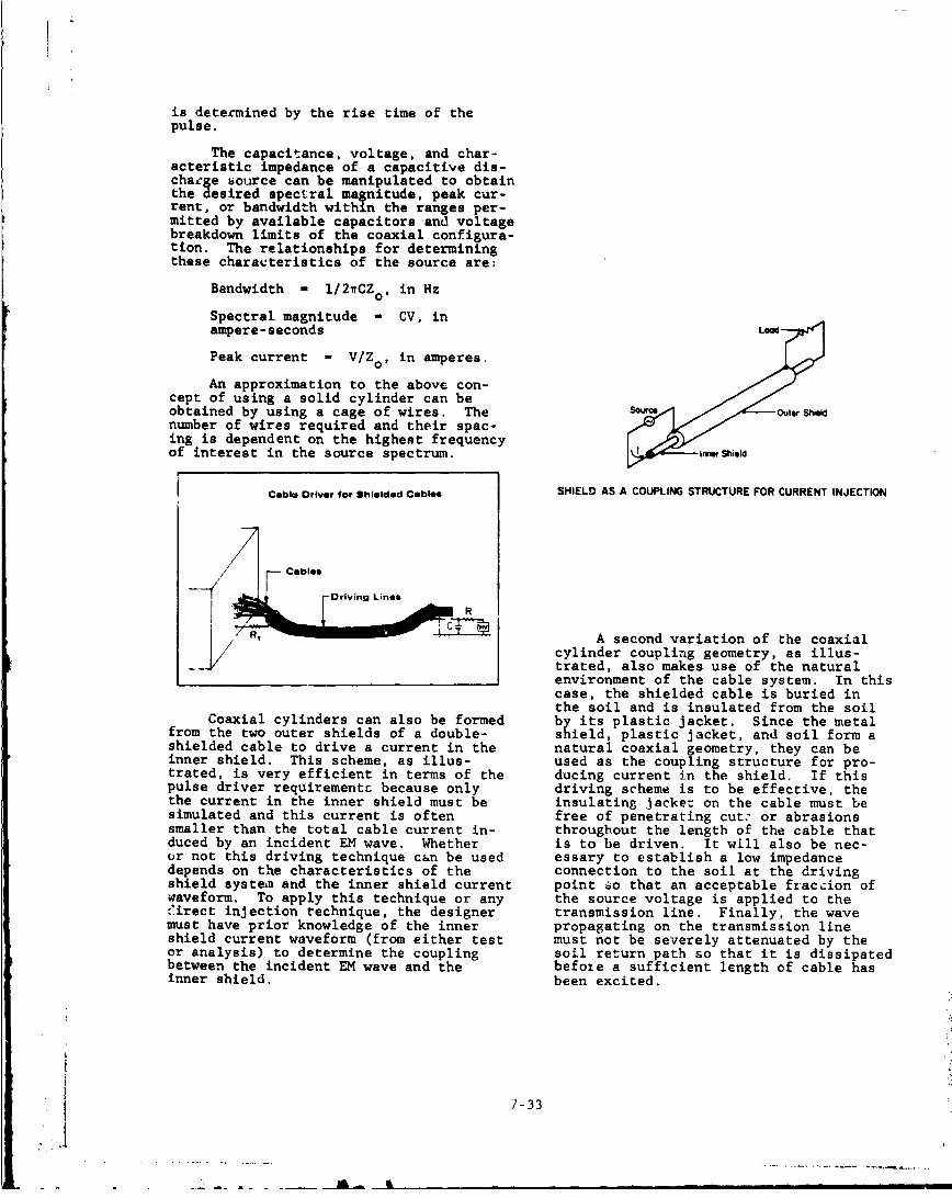
is determined by the rise time of thepulse.
The capacitance, voltage, and char-acteristic impedance of a capacitive dis-chaege uource can be manipulated to obtainthe desired spectral magnitude, peak cur-rent, or bandwidth within the ranges per-mitted by available capacitors and voltagebreakdown limits of the coaxial configura-tion. The relationships for determiningthese characteristics of the source are:
Bandwidth - l/2nCZo, in Hz
ampere-seconds
Peak current = V/Z 0 , in amperes.
An approximation to the above con-cept of using a solid cylinder can beobtained by using a cage of wires. Thenumber of wires required and their spac-ing is dependent on the highest frequencyof interest in the source spectrum. af ---- w ShilL
Cablo Driver for Shielded Cables SHIELD AS A COUPLING STRUCTURE FOR CURRENT INJECTION
.•R, A second variation of the coaxialcylinder coupling geometry, as illus-trated, also makes use of the naturalenvironment of the cable system. In thiscase, the shielded cable is buried inthe soil and is insulated from the soil
Coaxial cylinders can also be formed by its plastic jacket. Since the metalfrom the two outer shields of a double- shield, plastic jacket, and soil form ashielded cable to drive a current in the natural coaxial geometry, they can beinner shield. This scheme, as illus- used as the coupling structure for pro-trated, is very efficient in terms of the ducing current in the shield. If thispulse driver requirementc because only driving scheme is to be effective, thethe current in the inner shield must be insulating Jacke: on the cable must besimulated and this current is often free of penetrating cut. or abrasionssmaller than the total cable current in- throughout the length of the cable thatduced by an incident EM wave. Whether is to be driven. It will also be nec-or not this driving technique c&n be used essary to establish a low impedancedepends on the characteristics of the connection to the soil at the drivingshield system and the inner shield current point ýo that an acceptable fraccion ofwaveform. To apply this technique or any the source voltage is applied to thedirect injection technique, the designer transmission line. Finally, the wavemust have prior knowledge of the inner propagating on the transmission lineshield current waveform (from either test must not be severely attenuated by theor analysis) to determine the coupling soil return path so that it is dissipatedbetween the incident EM wave and the befoxe a sufficient length of cable hasinner shield. been excited.
7-33
AL a
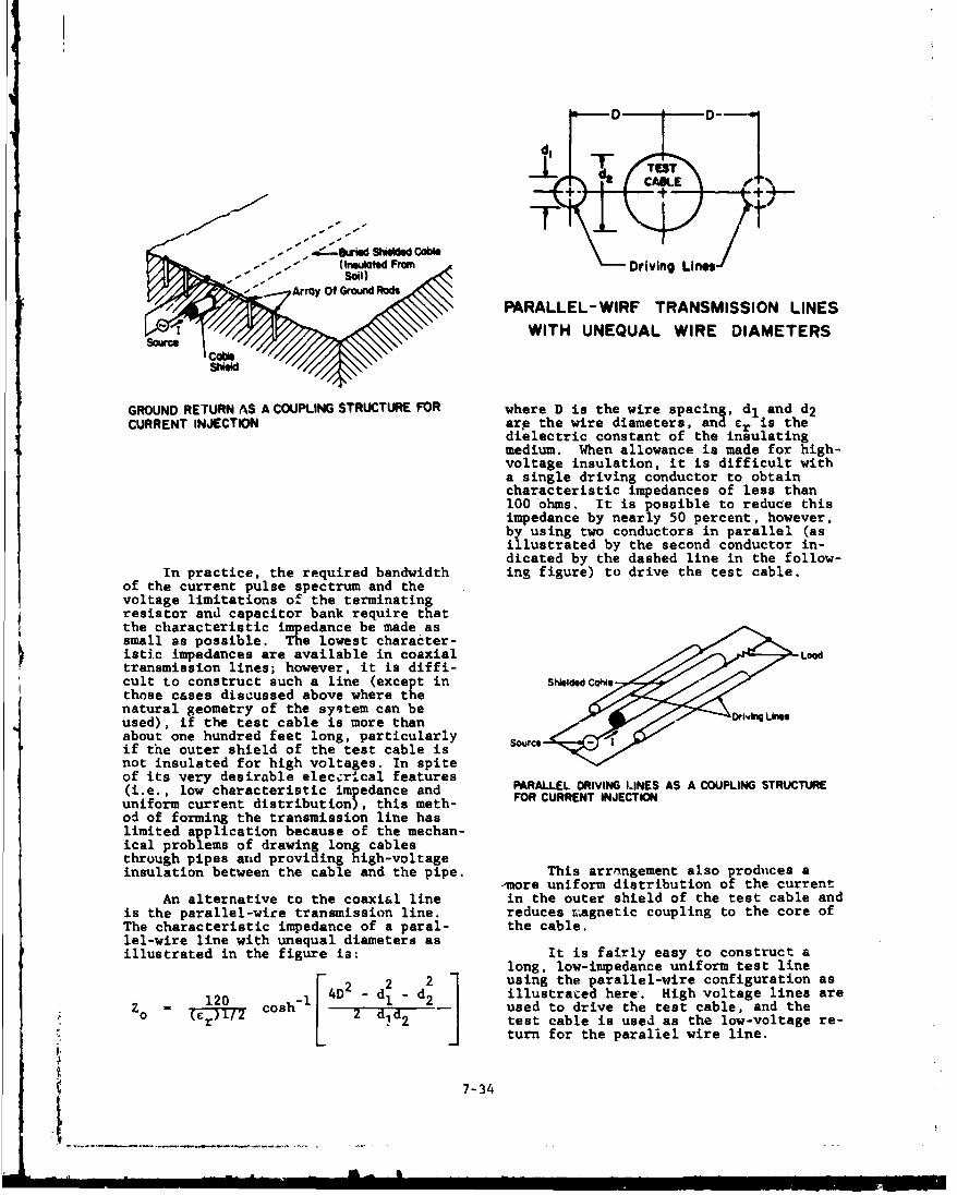
0---D -D-•
d.lt--csrtdShtoediOs"•asigled(rimincd Fonm Drivinu Lines
bAryy Of Grtwo Rocss
illusrate byte eon'onuto n
• •\\•".PARALLEL-WIRF TRANSMISSION LINES
Cab V WITH UNEQUAL WIRE DIAMETERS
GROUND RETURN AS A COUPLING STRUCTURE FOR where D is the wire spacing, dt and d2CURRENT INJECTON are the wire diameterst and hr is the
dielectric constant of the insulatingmedium. When allowance is made for high-voltage insulation, it is difficult witha single driving conductor to obtaincharacteristic impedances of less thans00 ohms. It io postible to reduce thisimpedance by nelrly 50 percent, however,by using two conductors in parallel (asillustrated by the second conductor in-dicated by the dashed line in the follow-In practice, the required bandwidth ing figure) to drive the test cable.
of the current pulse spectrum and thevoltage limitations of the terminatingresistor and capacitor bank require thatthe characteristic impedance be made asifsmall as possible. The lowest character-istic impedances are available in coaxial Roodtransmission lines; however, it is diffi-cult to construct such a line (except in SN*fd aedthose cases discussed above where thenatural geometry of the system can beused),uif thetest cable s morethan producesabout one hundred feet long, particularlyif the outer shield of the test cable ise andnot insulated for high voltages. In spite zof its very desirable electrical features lineE reduces LINE S c l t the CoRE(i.e., low characteristic impedance and paraC-RAEt cINalIe. INuniform current distribution), this meth-od of forming the transmission lIne haslimited application because of the mechan-ical problems of drawing long cablesthrough pipes and providing high-voltageinsulation between the cable and the pipe. This arrangement also produces a
-more uniform distribution of the currentAn alternative to the coaxi&l line in the outer shield of the test cable andis the parallel-wife transmission line. reduces ragnetic coupling to the core of
The characteristic impedance of a paral- the cable.lel-wire line with unequal diameters asillustrated in the figure is: It is fairly easy to construct a
long, low-impedance uniform test line2 2 2 using the parall el-wire configuration as
z120 coh14D2 dI - d2 illustrated here'. High voltage lines are"o C)/ used to drive the test cable, and theZo (r)/ i~h- 2 2 test cable is used as the low-voltage re-
S~turn for the parallel wire line.
7-34
m. a

A variation of the parallel-wiredriving structure is useful for drivingshielded cables with insulating jackets ••-cthat are routed along a metal structureor laid in metal cable trays as illus-trated,
ibroidal Core
Oulkh*W-Structural Ground (Both Ends)
CURRENT TRANSFORMER TO INJECTCURRENT ON A GROUNDED CABLE SHIELD
The equivalent circuit of an N turn
Equ~ &iund ftnprimary and single.-turn secondary cut-renttransformer referenced to the primary isillustrated below. Ll and C1 are theprimary inductance and stray capacitance,
EQUIPMENT GROUND AS A COUPLING STRUCTURE Rc is the core loss resistance, Lc isFOR CURRENT INJECTION the core leakage inductance, and L2 and
U2 are the secondary inductance and straycapacitance.
I l, - L i N aL l I t•
The configuration has the character- -Nt
istics of a symmetrical two-wire trans-mission line, since the ground plane canbe replaced by an image conductor to forma two-conductor line having twice thecharacteristic impedance of the conductor EQUIVALENT CIRCUIT OF A TOROIDALand ground plane. This method of driving CORE CURRENT TRANSFORMERthe shield is limited to applicationswhere one end of the shield can be removedfrom the ground and covinected to the en-ergy source. In cases where simulatlonis required, it has the advantage thatmuch of the pulse shaping is accomplishedby the system structure, if the cable Unshielded Cable Driving Techniqueslength and terminations are preserved. The current transformer concept can
If both ends of the cable shi-ld are also be used for driving individual orgrounded to the structure in the system, multiple unshielded wires. For unshieldedand it is desired to nreserve this trans- cables, signals can also be injected si-mission line configuration so that the multaneously on all or individual wiresgeometry of the system will shape the by small capacitance as is indicatedcurrent waveform, then the current may be here. The cables are placed within ainjected by means of a current cransform- conducting cylinder that forms the driveer constructed as illustrated in the side of each coupling capacitance. Thisfollowing figure. The toroidal core can scheme is an easy method to loosly coupleb.' split and clamped around the cable energy to multiple wires without disrupt-
Swithout distrubing the cable system. ing the normal circuit operation.
7-35

accessible), each condlactor in the inter-Cable Oriver fot Unshlieded Cable* connecting bundle might have to be
driven in vidually. Usually, it ispossible to rank the importance of theindividual wires in terms of the sus-ceptibility of the circuits served by
FIP' the wire so that precise simulation isnot necessary for every wire in the4a53. bundle.
Direct Injection on Signal-Carryinx Con,-h Voltage ductors
power supply
The injection of the test signalinto signal-carrying conductors, such astha core conductors of a shielded cableor the conductors of an unshielded cable
This approach to simulating voltage or equipment termiuials, usually requiresinjection into unshielded cable bundles a more carefully designed experiment thaninduces currents that simulate the common- the injection of test signals into cablemode current that was measured in a low- shielda. Most tests in which the cablelevel test of the complete system and shield is driven utilize loose couplingassumes the currents will distribute prop- between the driving source and the signal-erly between the individual wires in the carrying co~iducto-s because the shleldbundle. Although this approach is use- usually provides more than 20 dB of iso-ful, particularly in the early stages of lation. Because of this loose coupling,the system test, the results can be mis- the syotem impedances that affect theleading. Interconnecting cables between resnonses of the signal-carrying conduct-equipment cabinets within a shielded en- ors are not significantly affected byclosure are often excited by currents the driving system and the responsesconducted along a cable or along some of essentially occur from natural excitationthe wires in the cable rather than by of the cable shield. When the test sig-coupling to ambient EM fields. Conse- nal is injected directly however, thequently, the current in the individual driving source and coupling-system im-wires is not necessarily determined by pedances may alter the system response.specifying the total current in the bundle Thus, additional effort may be requiredand the individual wire terminations, to evaluate the effect of these differ-For example, assume that a bundle with ences - that is, to determine the systemmany conductors contains some conductors response had the effects of the injectionthat are connectid to circuits outside a system not been present or to placeahielded enclosure as well as to some bounds on the possible effects of thethat are intercomnecting conductors for injection system.circuits totally within a shielded en-closure. Thus, the interconnecting bundle Direct injection of test signals oncontains some conductors that are tight- signal-carrying conductors of shieldedly coupled to the conductors in the ex- cables also requires a more comprehensiveternal bundle. In such a case, it is understanding of the interaction of theprobable that the excitation of the inter- system with the electromagnetic pulse,connecting bundlk will be dominated by inasmuch as the designer must be able tothe signal on those wires from outside deterri.ine (either through analysis orthe shield and that the signal on the experiment) the EMP signal that couplesremainder of the conductors in the inter- to and penetrates through the cableconnecting bundle will result primarily shield. For unshielded cables, antennas,from mutual coupling among the conductors, and power lines directly exposed toA bulk common-node current injected into electromagnetic radiation, however, thethe interconnectIg wire-bundle, there- problem of specifying the pulse shapefore, will not produce the same system may be no more difficult than that ofresponse in the equipment as the bulk specifying the pulse shape for shieldedcurrent prc¢duced by the EMP environment, cables. The quality of simulation re-
quired (o= t',e analysis needed to justifyIn the case described above, the the quality ¢' simulation used) may also
bulk-current injection would proeuce a be consideratly greater for direct in-much more effective simulation if it were jection into signal-carrying conductorsmade on the wire bundle entering from 1ýcause all pulse shaping must be accomp-the external equipment. If it were not lished by the driving source and couplingpossible to inject the tust pulse into network. The designer cannot take ad-the external conductors (for example, vantage of the pulse-shaping and looseonly the interconnecting bundle was easily coupling characteristics of the shield as
7-36
A

is the case when testing with inj&ctionof currents on cable shields.
Direct injection (hard wire connec-tion) of common mode voltages into indi-vidual wires of a cable bundle or directlyat the equipment terminals can be achievedthrough an impedance matrix as shown inthe following figure.
Conduit OfSysttm From*
IMPEDANCE MATRIX USED TO INJECT COMON-ft WE VOLTGES Suc
CAPACITORS USED TO INJECT COMMON- MODE VOLTAGFSThe impedance matrix should simulate
the normal impedances between the con-ductors and between the conductors andthe cable shield or system ground.
This method of driving cable con-ductors is perhaps the most straightfor-ward and coummonly used of all the direct At some suitable junction in theinjection methods. It nan also be used cable system, the energy source is capac-with unshielded cables that are routed itively coupled to the conductors and per-along a metal structure (such as an air- mitted to drive thext with respect to thecraft wing) or are placed in metal cable local ground or chassis. As illustratedtrays. With unshielded cables of this in the figure, however, the current in-type, the current is driven against the Jected at this point is divided into twometal structure or trays rather than parts, one flowing in each direction fromagainst the shield. One disadvantage of the injection point. Because this methodthis method is that the cable being driven of distributing the current differs radi-must be disconnected at one end; hence, cally from the current distribution thatthe system may not be operating in its would have. resulted from the EMP excita-normal state during the test. tion of the system, some care is required
in designing a valid test using this ap-When one end of the cable is not proach.
accessible, another injection method mustbe used. Such cases arise where discon- Direct injection at the equipmentnecting the cable piecludes .perating the terminals is often accomplished by drivingsystem in its normal mode - for example, terminal pairs or between a single termi-4isconnecting the main power leads to nal and ground. While this form of directinject a signal on these leads precludes irJoction does not provide the normal ex-operating the system from power supplied citation (all cable entries) of the system,through the leads. In these cases, it it is useful to determine damage thres-may be necessary to accept some compro- holds of individual circuits within themise in the quality of the simulation to equipment or subsystem. This form ofperform tests economically. One approach testing is applied principally to individ-that can be used under certasin conditions ual modiLle testing for compliance to anis illustrated in the figure. EMP sle oification.
7-3 1 A

The basic test set-up is presented the coaxial line impedance. The resistorin the following figure. absorbs the reflect ion that occurs at the
far end of the shorted line. The chargingcapacitor and resistor determine the pulsedecay time which is many microseconds.Thuý., the driving current contains consid-erable low frequencies. The reflection*
%"I VM].d.. M that occur in the line cre at frequenciessown .that are higher than those of iterest for
solid shield cables. If braid shields werebeing measured, the shorted end of theline could be terminated to give a fast,clean pulse rise. A typical test setup isshown in thh following figure for testingin the time domain.
Test
G.'t64r i)Sc sr I t u cp
hi Ch.!'
BASIC DIRECT 104JECTION TEST SETUP
Cf.hIW Prow
For this approach, the signal source suACIE TRANSFER iMEAC MEASUOINT Tfer SETuP FORis determined based on the test obiectives. TM DOMAINFor damage threshold testing, the systemshould be operating at the time of signalinjection. The unit should be terminatedin the act•,al load or a simulated loadwith the same respnuse. For upset ce&tinl.the unit under test must be operational.in this case, the terminal loading beingthe actual load is desirable. If this is The basic construction of the tri-not practical, a simulated load may be axial tester for use in these tests isused. The simulated load should have the illustrated in the following figure. Thissame frequency response characteristics configuration allows for a 1 meter lengthof the actual load. of cable to be tested which is the normal-
ized length for reporting the data.CW measurements are also commonly
used to assess system response to an ZMPp~tlse. Usually these tests consist ofmeasuring the pin-to-pin, or pin-to-caseimpedance as a function of frequency.The basic equipment for this type of test "consists of a swept frequency generatorand a net',ork analyzer that automaticallydisplays boti amplitude and ?hase of the - .equipment :erminal impedance.
Laboratory Component Tests - Cable Trans- -
ter Impedance
lransfer impedance measurements ofshielded cables can be made in the labor-story. The shield is driven as a part ofa transmission line, in this case a co-axial line. The storage capacitor is TR,• T,2T ,IXURI FOR SUWACE TRANIFt,discharged through a resistor that equals . C ,M-,WS
7-38
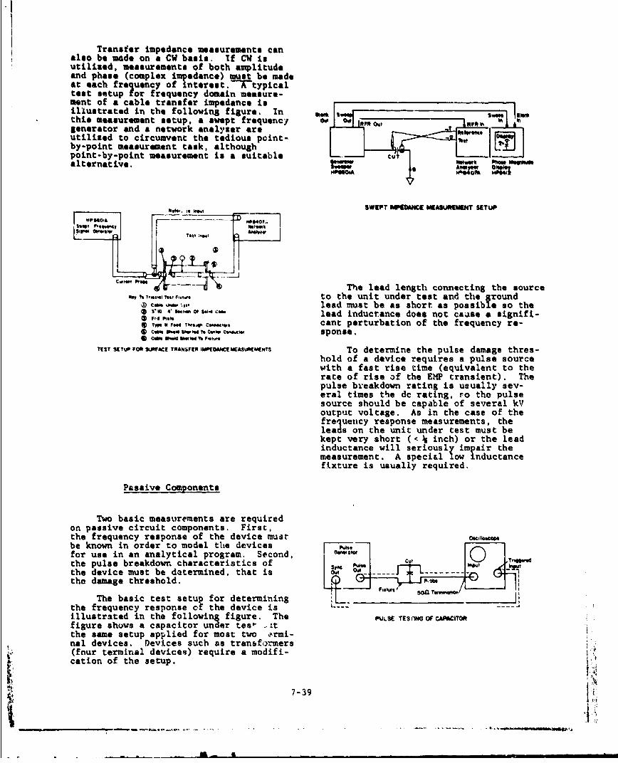
Transfer impedance measluremeHnts can
also be made on a CW basis. If CW isutilized, measurements of both amplitudeand phase (complex impedance) munst be madeat each frequency ofInterest.-T-typicaltest setup for frequency domain measure-mene of a cable transfer impedance as
illustrated in the following figure. Inthis measurement setup, a swept frequency OW~ 0.. O"generator and a network analyzer areutilized to circumvent the tedious point-by-point measurement task, althoughpoint-by-point measurement is a suitablealternative.
,0 Is WOOSWEPT 0W1CE MEASUREnENT SETUP
Ps"•-- - The lead length connecting the sourceft ,-., Viua T .. to the unit under test and the ground
0 C*~,W lead must be as short as possible so the( V-D 4'' t Of W Ca lead inductance does not cause a signifi-® F'.4 Pe404. Irv" itI' iAC....O.., cant perturbation of the frequency re-*D cimV"vfdT " ~ sponse,*D CGW R..w Ww~d e r
TEST SETUP FOA SACE TRANSFER, OE C MEASUREMENT$ To determine the pulse damage thres-hold of a device requires a pulse sourcewith a fast rise time (equivalent to therate of rise of the EMP transient). Thepulse breakdown rating is usually sev-eral times the dc rating, ro the pulsesource should be capable of several kVoutput voltage. As in the case of thefrequency response measurements, theleads on the unit under test must bekept very short (< )i inch) or the leadinductance will seriously impair themeasurement. A special low inductancefixture is usually required.
Passive Components
Two basic measurements are requiredon passive circuit components. First,the frequency response of the device must oa,,.be known in order to model the devices Pulsefor use in an analytical program. Second, 'WtCO0 TrWthe pulse breakdown characteristics of S _ Pustthe device must be determined, that is 0.ot fthe damage threshold.
The basic test setup for determining T
the frequency response of the device isillustrated in the following figure. The PULSE TESrWGOFCAWITORfigure shows a capacitor under tee' .-tthe same setup applied for most two •rmi-nal devices. Devices such as traneformers(four terminal devices) require a modifi-
a. cation of the setup.
_ _ _ __ .... 7-39 -
S... ... a

1he test procedure for the low-leve! By knowing the 'S" parameters, thefrequency domain characcerization of fil- filter response for any waveform and in-ters is the measurement of the S para- puc and output terminations can be deter-meters. Based o~n the t'-pical WMP-induced mired analyticaliy. This is essentialtronsients, these measurements should be since the loads are not purely resistiveperformed at least over a very wide fre- over tl' entire frequency range of inter-uency range. This procedure considetas est,evelopment of scattering parameters by
reflectivity measurements. An alternate To obtain the damAs- threshold forprocedure considers development of scat- filters, the concept illustrated is em-tering paramet.srR by impedance measure- ployed for low oi high pass filters.ment techniques. Both procedures are This concept requires a high voltage pul-applicable ovexr the frequency range of set with a fast rise time. It is notinterest, generally from 1 kHz to 100 adequate for narrow band pass filtersM. However, the reflectivity measure- since the energy spectral density in thements are mcre appropriate for frequencies filter pass band is generally insufficientabove 100 kHz, partly because of equip- to produce filter breakdown. In thisment availability. Above 10 MHz, the case, a high level pulsed kF aource wouldreflect.vity measurements can be more be more appropriate. The test should beaccurate ,nd simpler than impedance conducted for both ports of the filter.measurements,
The S parameters reduce to voltagereflection and transmission coefficientswhen characteristic impedance termina- 5oA Devicetions and source impedances are employed. pulvse Undo, 50Therefore, the S-parameters can be easily Generatot Ttmeasured with commercially available testequipment,
One of the standard circuits for PULSE TEST PROCEDURE FOR FILTERSmeasuring S-parameters is shown in thefollowing figure.
A,
a) Terminal Protective Devices
son Two sets of measurements are re--u quired to characterize the performance of
terminal protective devices for EMP appli-,c / cation. First, a set of quasi-static
measurements is required to evaluate thestatic breakdown, extingulshing voltage,follow current, etc., of the device, A
STANOCACIRCUITFOR MEASURINGS-PARAMETEtrS typical test setup is shown for measure-ment of the static breakdown voltage,
2o Mn Iba
IPower .0FC'ý - Prowtor Under Testjsupply ~ 4~j
The setup shown, that is, the gener-ator connected to port 1, provides theSll and S21 measurements. Connecting the TYPICAL CIRCUIT FOR MEASUREMENTOF VS8generator to port 2 provides the S12 andS22 parameters through the relationships
S12 B "L
22= D C "-D
7-40

* The capacitor is incorporated so thepower supply is not damaged due to the W ... Troi,,ttig LOOP Spacedshort circuit current when the device of L, 2.5n. 0 W
fires. To determine the extinguishing svoltage, q second rcgulatcd, -cotectedsource is required. I
The second set of measurements re- / Retractable Coble
lates to the device capability to respond /Pickuto a transient with a fast rate of rise. /Ale-
In this case, a high voltage pulse gener-ator with a variable rate of rise is re- h/Dc..uired to determine the response time asshown.
Since a short duration pulse is uti- A Thermo-Ammet.rlized in this approach, the short circuitcurrent is usually not a problem if the Unlv r I
pulser is protected (current limited). Trom, VLF OscillatorAgain, since a transient is involved, leadlengths must be kept short to eliminate NOTES: C h lIlooorer
Pickuploo I~o n plant of large loop or center of
the effects of lead inductance. Usually D-. .I enclosure
low inductance fixtures must be fabri-cated to assure valid test data. ALSO C. h-D
D0 h-C
LARGE-LOOP TEST SETUP
VariablePulse 50fllo
Generat,)r Aeutor OaVl 1
Test Device
TYPICAL CIRCUIT CONFIGURATION FOR MEASURING Vpq To determine the high frequency re-sponse, the test setup illustrated isutilized ½n the UHF (30-300 MHz) band.This approach tests the enclosure on apiecemeal basis and again is good for a
A frequency response measurement is relative measurement in the laboratory.also required to determine the nor-al in- It will revreal flaws in the enclosure.sertion loss of these devices. Thismeasurement car. be performed by the sameapproach as for passive devices.
Shielding Measurements Field Strrngule Meter
Shielding measurements are requiredon a variety of enclosure sizes. Ideally, ,the enclosure would be exposed to planewave fields in one of the simulator types O•c0•, h/2
previously discussed. Many times, how- A,,,cuoto,
ever, it is desirable to evaluate theenclosure performance in the laboratory. ' -Standard measurement procedures are avail- k I
able. -rLine Strercher Fora l Generator Matching
Room size enclosures (a few meters Electrical Tape Signal Generator
on a side) can be evaluated in the low 3m B W
frequency (< I MHz) region by the large h/2 -Or-loop test setup illustrated. This pro.-cedure, while no* providing the shieldingeffectiveness fo. plane waves, does ex- Whichever Is The Grealt
cite currents c. all faces of the enclo- .o,.sure. This would locate such features as C."X/8poor seams, door gasketing, etc. This c, 2We a
approach can provide for good quality CUR2mOrEXWh,cheEer I Greater
control if the enclosure shielding ef- UHF MEASUREMENT SETUPfectiveness has been certified by planewave illumination..
7-41

Measurements of seam performance, Using a standard fixture, the gasketdoor L.•sketing performance, or locating performance can be documented on a norm-apertures, etc., can also be performed alized transfer impedance (ZTN) given byusing the small loop concept illustrated.This concept measures the shielding ef- = ZT) X ohm-metersfectiveness in the lccal area of the loop. ZTNBy probing the enclosure, flaws can be wherelocated. V (w) ohms
ZT(W) =
V (w) - coupled voltage acrossIS the inner surface of the///0.3. i om 0ioýO .O M 0O. 3m / gasket
O,,CioIt I A, efto, I (w) sheath current across theexternal part of thegasket
Thmd Wi,. TwovW - gasket length.
The test setup for performing these
s.,,tm Sirf. measurements requires only standard labo-ratory instrumentation, plus a wellshielded enclosure as illustrated. The
SMALL-LOOP TEST SETUP pulse source rise time and duration mustbe selected to provide a spectral contentat least as wide as the EMP transient.
The independent determination of S.ope
gasketing performance is often desirable.To relate the relative performance ofvarious types of gasket materials, a stand- L 000
ard fixture, as illustrated, is required. 50, S. T.% So p.
PREFERRED TEST SETUP FOR GASKETS
BolE. t, CffroSS-ECO oisSTFXT
USING SACKsI4EL SHIELD Evaluating the shielding effective-
ness of vents (honeycomb, screens, etc.)is another important aspect of shieldingmeasurements. Again, a standard testfixture is required to obtain relative
performance, as illustrated.
7-42

A tri-plate line is utilized forgreater uniformity of the incident field.Utilizing a tri-plate structure with anar~ower center plate reduces fringing of
__---___--- the field at the edges of the line pro-vent vidin a plane wave over the vent being
testel.
11i The setup shown is for the E-fieldpolarization normal to the plane of thevent. ror complete assessment of the
I •gasket performance, the other orthogonal3-6X0./Dff - polarl.zations of the E-field should be
ferfefence -,e used. This can bt accomplished by theTrameito LIMsame concept with alternate configurations__ of the illuminating structure.
Semiconductor DeviceQ Damage Threshold Testing
OuiplayAMP
Discrete semiconductor device damageRecording Equip. Ago thresholds are normally obtained for the
b-e Junction as discussed in Section IV.The normal procedure is to test the de-vice to destruction using a laboratory
SUGGESTED T!XT FIXTURE pulse generatur as a source, as illus-trated.
A tri-plate transmission line is used Curveas the exciting source in determining the Tracershielding effectiveness for plane waves--as is illustrated below.
Pulse
Generator
terminal oaIoryC.S~ScopeTriplete psrsaaloFlush
LIn. Wih Enclour
LineWithEnclsureSEMICONDUCTOR TEST SETUP
The pulse source should have both avariable amplit ci2 (for step testing) andpulse width so we time dependence (slopeof the damage curve) can be obtained. TheSource | Shiel Room setup shown is manual operation. A simi-
lar setup can be used for evaluating eachterminal of an IC.
Current limited pulsers can also beused to advantage. Such pulsers couldhave the short circuit current limited toa value such that when the semiconduc:torgoes into thermal second breakdown, thecurrent through the device is below that
U T T Trequired for destruction of the junction.SUGGESTED EXTERNAL TEST
i 7-43

If a large number of devices are to The system for receiving and re-be tested, automated test procedures cording scale model measurement wave-should be considered. Automated test set- Corms consists of sensors, a samplingups for making these measurements are oscilloscope operated in the triggeredavailable at the Air Force Weapons Labo- mode, and an X-Y recorder to display ýheratory. data. Sampling oscilloscopes can easily
have rise time capabilities of 3 x 10-11seconds. To trigger operation from a
7.6 DIMENSIONAL SCALE MODELING TECHNIQUES repetitive energy source, however, it isnecessary tu use a delay line in thesignal channel to compensate for sweep
EM scale modeling of systems to de- delays in the oscilloscope. This delaytermine their responses to transient EM l.ine tends to limit the signal r4ýanneLfields is generally limited in the choice rise time to no better than 101"v seconds.of the scaling parameter by availabletransient energy sources. When these Electric and magnetic fields andsources are in the form of switch dis- the currents on conductors and conductingcharged capacitors, they can achieve tran- surfaces of the models can be measured.sient rise times of the order of 10-10 Small capacitive probe antennas utilizingseconds through the use of mercury-wetted anodize as a dielectric such as that il-reed type relays with contacts under gas lustrated can be used to sense the elec-pressure in a coaxial geometry as illus- tric field that is normal to a conductingtrated. The capacitor is charged through surface. Such a sensor can have suffi-the charging resistor and discharged cient capacitance to drive a coaxialthrough the coaxial gaometry, which is cable with a low frequency limit that isformed by the switch and switch housing. adequate for observing transient pulseThe capacitor can be replaced with co- widths of 20 ns. The sensor rise timeaxial cable to forta square output wave- can be less than 10-il seconds.forms and the entire system can bedesigned to operate at the coaxial cableimpedance. Energy sources of the typeillustrated can be constructed to produceoutput voltages from 1 to 4 kV. Theycan be easily converted to repetiti"'epulses at ac power frequencies, and beirgsingle-ended, can drive any scaled fieldsimulator that has a single-ended input(for example, a monopole or parallel-plate Metaltransmission line). By utilizing a balun,a long dipole can be used to radiate EM Dielectricenergy at any incidence angle or polari-zation. MetaI
voCapacitor Output
Coil Connector
ELECTRIC FIELD SENSOR
Charging Mercury-Resistor Wetted
SwitchCommercially available probes for
SCALE-MODELING TRANSIENT ENERGY SOURCE �easuring current density, J, or mag-netic field, B, with a small slot antenna,as illustrated in the folliwing figure,have approximately 3 x 10⁻¹⁰ second risetime so the current measuring capabilityis the limiting factor in setting thescaling factor if the electromagnetictransient rise time is to be observed.Special small loops can be constructedto improve the current and magnetic fieldmeasurement rise time; however, theygenerally have decreased sensitivity,which limits their application in scalemodel measurements.
7-44

less than 50 will be required if thescale model measurements are to observethis rise time. For large systems, itis desirable to use larger scale factrnrs.Fortunately, such factors can be used be-cause the rise time response of systemsis approximately the excitation riss time
Current Probe •convolved with the time corresponding tothe dimensions of the system that are
J parallel to the incident field polariza-tion. When using scale factors that givea faster response than the measuremertsystem response rise time, the data shouldbe checked to verify that the rise timeis not liinite,! by the measurement system.
When scale modeling transient EMcoupling, it is posuible to scale the EMPtransient wa-eform and thus obtain re-sronse data that can be directly inter-
MAGNETIC FIELD SENSOR preted for the transient response of thefull-scale system or for direct injectionwaveforms. Tn scale modeling EM fieldsimulators or an entire system to deter-mine the response of the components ofthe system, it is often convenient to usea short (or impulse-like) transient so
EM scele modeling of a sysuem entails that clear times and system responses cana scaled construction of the conductive be separated. The following figure showsand EM features of that system. The vari- an example of this approach for a modeledous parts of the system are duplicated in monopole. Both the clear time and theminiature. However, only those feaLures multiple reflections on the monopole arethat define the EM characteristics need directly observed and can be interpretedbe properly sca]ed. Generally, only those in travel times on the scaled model.features that can have a first-order ef-fect on the interaction of the system withthe incident wave must be reproduced inthe scale model. Features that havelittle effect, such as internal conductorsand small apertures, do not need to bereproduced; however, if they can be easilyscaled, they may improve the fidelity ofthe mcdel. EM scale modeling thus isused to study the gross features of thesystem that control the total system re-sponse. Secondary energy coupling effectsthat occur within the system are usually ENDnot readily amenable to scaling. - -.
models, EM planes of slmmetry can some- -IM-
times be utilized to reduce the model. sizeand to provide shielding for the instru-mentation. Generally, symmetry planescan only be utilized when modeling simu- SCALE MODEL MEASUREMENT OF MONOPOLE REFLECTIONSlators and very special systems such asmissiles or aircraft. The conductivematerials used in scale models are comnoTL-ly copper sheet and wire, tubing, andmesh. Earth is modeled by adding salt toreal earth to increase conductivity. Di-electric materials are generally modeledwith plastics or wood.
The scale factor selected for model- For observing the natural responseing an EM response (or coupling) problem of a system, it is preferable to use adepends on the pu.pose of the modeling long square wave with low frequency ener-test. If the response caused by a 10-8 gies so that the system's natural reson-to 10-9 second transient rise time is to ances can be observed. The figure showsbe investigated, ,hen a scale factor of the response of a system to a short (im-
7-45
- L .Ilk

IF
pulse-like) transient and Its response Housed beneath the facility is ato a long, square-wave transient. The shielded instrumentation room containingsquare-wave response is the integral of date recording and monitoring instru-the impulse response and provides a direct mentation. In eddition to hardwire datameasurement of the late-time (low frequen- links, a multichannel microwave data linkc'1) rceponsc .harac-.ristics that -re not is alco avLilab!e.easy to observe from the impulse responsc.With careful interpretation, almost anytransient that excites the scaled systemcan be uaed to determine the responsecharacteristics of that system.
Sq.arWrI
Wave
In,,,,o =v. _ --RnResponse
SYSTEM IMPULSE AND SQUARE WAVE RESPONSE
TRESTLE
The TRESTLE simulator is presentlyunder construction at Kirtland Air ForceBase, New Mexico. It is similar in ap-
7.7 SIMULATION FACILITIES pearance to ARES, but considerably larger.It will produce fields in excess of 50
As an aid to the reader, brief des- kV/m over an interaction volume of approx-criptions of representative large scale imatoly 80 1 x 80 w x 75 h meters. TheEMP simulators are presented. Tables unique feature is a trestle for support-listing the basic characteristics of ing the system under test in the centerthese and additional simulators is also of the interaction volume.provided.
Bounded Wave Simulators ALECS
The AFWL-LASL Electromagnetic Cali-ARES bration and Simulation facility is a
bounded-wave transmission line simulatorThe Advanced Research EMP Simulation located south of the east-west runway at
facility is another bounded-wave trans- Kirtland Air Force Base, New Mexico. Themission line simulator. ARES is a DNA working volume is 13 m high, 15 m long,facility located on Kirtland Air Force and 24 m wide. The transition sectionsBase, New Mexico. The normal working are 50 m long. The line impedance isvolume is 40 m high, 30 m long, and 40 m 95 0.wide. The transition sections are 76 mlong. The line impedance is about 100 Q. The electromagnetic pulse is pro-
duced by discharging a graded capacitorThe ARES pulser has a nominal charg- stack into a short, 41-s coaxial trans-
ing voltage of 6 MV and energy storage mission line (the peaking capacitorof 50 kj. The peak output voltage is 45 concept) and by discharging this series-Mv maximum. The energy source is a co- combination into a transition structureaxial line storage element and a Van de that mates with the ground plane andGraaff generator power supply. parallel-wire top plane of the array.
The 41-R coaxial line provides for theField strengths on the order of ap- initial, nanosecond rise time of the
proximately 110 kV/m are obtainable in wave, while the graded capacitor stackthe interaction volume. The pulse rise provides for the large amount of energytime is 6 nsec. The pulse width is vari- in the remaining portion of the wave.able from 100-500 nsec. The pulse launching system is energized
7-46
A a-

by a 2.2 Mv Van de Graaff generator priorto Atschaxgp, A triggered gap prcqidesabout one pulse per minute maximum.
The electromagnetic pulse that is "aMPdeli- ired tC, the working volume h_3 anapproximate 1.7 Mv peak voltage, a rise Toptime of approximately 6 nsec, and a 150- 0 Loodnsec decay (l/e). An experiment in the Pumerworking volume will see a peak E-field ofup to approximately 125 kV/m. -
I-225 Fee~t - +-225 Feet---An underground, shielded room contains Side
diagnostic instrumentation to implementthe desired testing programs. Hardwireinstrumentation links may be routed from Goundthe working volume of the simulator andthe instrumentation room.
The ALECS instrumentation system con-sists of a ten-channel microwave-datasystem, a hardwire data system, a tracerecording system, a timing and firingsystem, and attendant checkout and moni- TEFStoring equipment. Most of the above sys-tems are housed in the double-walled,welded-seam, sheet-steel shielded rooms The Transportable Electromagneticthat afford a 120-dB attenuation. Field Simulator is a bounded-wave trans-
mission line simulator with multiple feedsthat is designed to propagate a transientin the vertical downward direction. Five-hundred and seventy-six transition sec-tions, each with a line impedance of 2000 are used. Four transitions are paral-leled and driven from a 50 Q cable.
The cables (144 total) are commonlydriven from a single switch and capacitorbank. The 144 sections can be configuredin a variety of ways to illuminate anarea of 40 x 40 meters. A field of 50kV/m is provided with a 4 nsec rise timeand a decay time constant of 350 nsec.
Versions of this simulator are avail-able at the White Sands Missile Range,New Mexico and the Naval Surface Weapons
HEMP Center/White Oak Laboratory test facilityat Patuxent Naval Air Station.
HEMP is another bounded-wave trans-mission line simulator located at theWhite Sands Missile Range, New Mexico.This simulator does nut have a workingvolume section. The two transition sec-tions are each 68 m long. The line di-mensions where the transition sections meet Conical Transmission.is 15 m high and 24 m wide. The line im• Line orpedance is 135 Q.
The transient source is a 10-stageLC generator that can provide voltages of Metal Mesh - Skirt50 to 400 kV. At 400 kV, the peak elec- Skirttric field is 26 kV/m with a 3 nsec rise Test Objecttime. The transient decay time constantis about 300 nsec.
7-47
S. .,I•, , :

SEIGE The te-t WhJacr. (au chas a missile)is positioned approximately 100 feet from
The Simulator Induced EMP Ground the antenna and 10 to 20 feet above theEnvironment simulator is a bounded-wave ground. Under these circumstances, thetransmission line simulator with multiple system undeL test would see a peak E-feeds or transition sections. This simu- field of approximately 1000 V/m.litor is designed to test a buried sy3tem.The working volume is 3 m high and usesthe earth for the lower plate. Four 80-9transitions drive the lire. One versionof this simulator is at the Air ForceWeapons Laboratory, Kirtland Air ForceBase, New Mexico.
Woo yn.Iis /oae tOlno lrd.Ti
i ehH@
.n A . .n
sf e l o g a
G-14
9 r ~pnd AIRo fl
T-
twoPW
Pd5 T- Anyris FMartin-Marietta Long-Wire
aThe Martn Marseta mLong-Wire facil-i is located at Orla9ndo, rlorida. Thisfacility is similar to the Sandia Long-Wire The antenna is 1000 feet long and46 feet above the ground. It is poweredby two 1eMi5 kV power supplies, and coronarings are used to minimize corona losses.
Longt Wire Dipole Simulators The spark gap uses a mixture of 6percent oxyger and 94 percent nitrogen,under pressure (50 to 5000 psi). By
Sandia Long-Wire varying the pressure, the spacing of thegap, the charging resistance, and the
One of the first EM6 simulators con- voltage, it is possible to vary the pulsestructed was the Sandia Long-Wire. This repetition frequency, the amplitude offacility, located on Kirtland Air Force the radiated field, and the rise time ofBase, New Mexico, was designed and con- the pulse.structed by the Sandia Corporation. Thissimulator is a horizontal dipole radiator The pulse rise times can be variedwith discrete lumped loading resistors. from 5 to 30 nsec, and the pulse widths
can be varied from 100 to 700 nsec. Max-The "long-wire" in the Sandia Long- imum peak E-field intensity is 1100 Vim
Wire was actually a 6 inch diameter, alu- at a point 100 feet from the antenna.minum irrigation pipe. Fifty sections Pulse repetition rates of 10 per secondof this pipe, each 20 feet long, were are possible.joined to form a 1,000 foot long-wireantenna. The antenna was supported bytelephone poles, 40 feet above the ground. .......:,Two 20 kV, dc-power supplies wereconnected to a pressurized parallel-plateswitch. Each half of the antenna ischaiged by the 20 kV power supplies, withone side posi-T4 .ve and the other negative,The center switch ther, would break downat a voltage level as determined by thegas pressure and gap separation. Theout put pulse is approximately that of adouble exponential, with a rise time ofless than 10 nsec, and a decay time (peak,.to 10 percent) of approximately one micro- -.-- yLMFAU1 11PI
second.
7-48
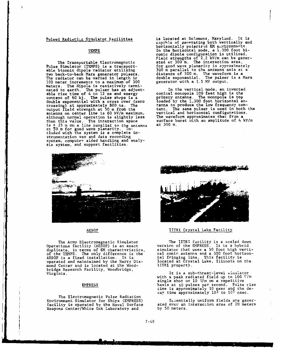
Pulsed Radiati:.g Simulator Facilities is located at Solomons, Maryland. It iscapnble of genprating both vertically andhorizontally polarired EM e,,vironmerts
TEMPS In the horizontal mode, a 1.300 foot bi-conic dipole configuration is utilized.Field strengths of 2.2 kV/m can be gener-
The Transportable Electromagnetic ated at 300 m. The interaction area,Pulse Simulator (TEMPS) is a transport- for good wave planarity is approximatelyable biconic dipole radiator utilizing 300 m parallel to the antenna axis at atwo back-to-back Marx generator pulsers, distance of 300 m. The waveform is aThe radiator can be varied in length in double exponential. The pulser is a Marx100 meter increments to a maximum of 300 generator with a 2.5 MV output.meters. The dipole is resistively termi-nated to earth. The pulser has an adjust- In the vertical mode, an invertedable rise time of 4 to 12 ns and energy conical monopole 100 feet high is thecontent of 60 kj. The pulse shepe is a primary antenna. The monopole is topdouble exponential with a cross over (zero loaded by the 1,300 foot horizontal an-crossing) at approximately 800 ns. The tenna to produce the low frequency con-output field strength at 50 m from the tent. The same pulser is used in both theantenna on center line is 60 kV/m maximum, vertical and horizontal configurations.although normal operation is slightly less The waveform approximates that from athan this value. The interaction space surface burst with an amplitude of 4 kV/mis + 25 m on a line parallel to the antenna at 300 m.at 30 m for good wave planarity. In-cluded with the system is a complete in-strumentation van and data recordingsystem, compute'- aided handling and analy-sis system, and support facilities.
AESOP IITRI Crystal Lake Facility
The Army Electromagnetic Simulator The IITRI facility is a scaled downOperations facility (AESOP) is an exact version of the EMPRESS, It is a hybridduplicate, in terms of EM characteristics, simulator that uses a 50 foot high verti-of the TEMPS. The only difference is the cal conic antenna and a 300 foot horizon-AESOP is a fixed installation. It is tal fringing line. This facility isoperated and maintained by the Harry Dia- located at Crystal Lake, Illinois on themond Center and is located at the Wood- IITRI property.bridge Research Facility, Woodbridge,Virginia. It is a sub-threat-level 6i2Ulator
with a peak radiated field up to 100 V/msingle shot or 10 V/m on a repetitive
EMPRESS basis at 60 pulses per second. Pulse risetime is approximately 10 nsec and the de-cay time approximately 103 to 105 nsec.
The Electromagnetic Pulse RadiationEnvironment Simulator for Ships (EMPRESS) E&zentially uniform fields are gener-facility is operated by the Naval Surface ated over an interaction area of 20 metersWeapons Center/White Oak Laboratory and by 50 meters.
7-49

The coni.c antenna provides the high- CW Radiating Facilitiesfrequency, short-time transient and thefringing quasi-sratic f eld from the hori-zontal wire provides the low frequency WSMR Facilitie3or late time transient. The two radiatorsare driven from a common source to prcvidea vertically polarized test field. The U.S. Army at White Sands Missile
Ran e, Now Mpxirno, fta a 10 to 2C0 MHzIn the horizontal mode, the 300 foot CW facility that uses log periodic an-
fringing field line I s coivr~rt*.d to an tennas to obtain 1 V/r fields eitherearth termirated biconic dipole radiator. vertically or horizontally polarized.
0 .
RES HDL
The AFWL has a flyable Radiating The Woodbridge Reuearch Facility ofElectromagnetic Simulator (RES) that is the Harry Diamond Center at Woodbridge,a bh:cDn!.c radiator. The horizontul ver- Virginia opcrates and maintains a CWsion is 200 feet long and uses distribu- facility for coupling tests. The facilityted resistive coating on the dipole utilizes LPA antennas to provide approxi-elements to attenuate the antenna current mately 0.5 V/m fields over a frequencyto minimize :eflection.. The pulser is range of 3-100 MHz. The illuminated testa Marx generator with an output voltage area is approximately 30 x 30 maters atof 1.5 1AV. The oitput wa\eform is a a distance of 240 meters. The cransmitterdouble expone-tial. wave. The low fre- is a 200 watt power amplifier unit. Bothquency contex• is limited due ro the short vertical. and horizontal fields polariza-physical length of the antenna, Field tionG are available.strengths on the order of 1000 V/m at500 m art possible. The unique character-istics of this fscility are that it is Characteristics of Available Simulators.asily c-Lansportable, and beiltg airborne,can proidie all sangles of arrival of -heincident pulse. The following tables present data
on the existing simulators. Indicatedare tbc technical characteristics, thelocation, and the operational status.
L 7-50
MLi I I

WAVE- INTERACTIONNAME LOCATION FO&RM POL, MAGNITUDE VOLUME(X.wh) STATUS
BOUNDED WAVE SIMULATORS
ALECS Kirtland AFn, WM rxo V 50 kV/m 30x30xlO a Operational
ARES Kirtland AFB, NM Exo V 70 kV/m 40x30x"n m Opreational
80x80x75 a UnderTRESTLE Kirtland APB, NM Exo V >50 kV/m Modular up to Construction
TUFS WSMR, NM Exo V,H 65 kV/!m 40x4OxlO m Operational
TEPS NSWC/WOL, MD Exo V,H 50 kV/m Modular Operational
LONG-WIRE DIPOLE SIMULATiORS
SANDIA lOxlOxiO MLONG- (- plane wave-WIRE Kirtland AFB, NM Exo H 1 kV/m front) Unknown
MHO 10lOxIlO mLONG- (~ plane wave-WIRE Orlando, Fla. Exo H 1 kV/m front) Operational
INTERACTION ANGLEWAVE- DIRECT WAVE AREA OF
NAME . • N FkM POL. MAGNITUDE/DISTANCE (.Pl. Wave) ARRIVAL STATUS
RADIATING WAVE SIMULATORS
Portable, Deacti-RES I Kirtland AFB Exo H 1000 Arlm @ 500 M 100 m any vated
Portable, Deacti-RES II Kirtland AFB Exo V 1000 V/m @ 500 m 100 M any vated
Kirtland Opera-VPD AFP, NM Exo V 3 kV/m @ 200 m grazing tional
Area di-rectlybelowantenna
Kirtland (nonplan- Opera-HPD AFE, NM Exo H *50 kV/m @ 9 m HAC ar) normal tional
HDL HDL, Opera-Biconic Woodbridge, VA Exo H 15 kV/m @ 100 m - 200 m 100@200 m tional
HDL, Opera-AESOP Woodbridge, VA Exo 50 kV/m @ 50 m - 200 m 100@200 m tional
HDL, 5 kV/m @ 25 m Opera-VEMPS Woodbridge, VA Exo V (3.25 1V pulser) - 100 m 8razing .tional
NSWC 2.2 kV/m @ 300 m Opera-EMPRESS S,1lomons, MD Exo H (16 m HAG) - 300 m 80@300 m tional
*Directly below antenna (continued)
7-51
M&

INTER.CTION ANGLEWAVE- DIRECT WAVF AREA OF
NAME LOCArION FORM PC,. MAGNITUDE/DISTANCE GPI. Wave) ARRIJAI STATUS
RADIATING WAVE SIMULATORS
NSWC Sur- Opera-EMPRESS Solomons, MD face V 4 kV/m @ 300 m -300 m grazing tional
NSWC/NATC, Opera-EMPSAC Patuxent, MD Exo H 8.5 kV/m @ 50 m -25-jO m 17'@50 n tional
NSWC/NATC, In Con-NAVES Patux&nt, MD Exo V -11 kV/m @ 50 m -25-50 m grazing stuction
DNA,Transport- 50 kV/m @ 50 m Opera-
TEMPS able Exo H 12.5 kV/m @ 200 m -200 m 100@200 m tional
7.8 TEST INSTRUMENTATION AND SET-UP Signal Sensing
Signal sensing involves both themeasurement of the field enironment and
Up to this point, we have discussed the induced voltages and currents withintesting from the standpoint of generating the system. Both sensors and probes area simulated DIP environment. The next required to perform these measurementconsideration is monitoring the environ- functions.ment and the diagnostic instrumentationfor determining the effects of the en- Sensors refer to the measurement ofvironment on the system under test. The electromagnetic fields. These can be inprimary consideration will bc the nature free space to monitor simulator fields,of the instrumentation and the basic prob- within a conducting mediium such as earth,lems usually encountered, It will not or within equipment racks or buildings.
consider sensor design. Probes refer to the measurement of
Testing implies experimental obser- a voltage or current. Current probesvation of the EMP environment and the measure the total current flow in wires.system response; this means the measure- Voltage probes can be single ended refer-ment of transient electromagnetic fields, enced to a common signal line or can bevoltages, and currents. A complete uias- differential,urement system should include:
Sensors1. A signal sensing system The most cormonly used broadband
2. A distribution system electromagnetic field sensors are elec-trically small antennas, Such antennas
3. A recording system have the directivity characteristics ofa small electric or magnetic dipole and
4. A test plan and data reduction an impedance which is predominantly re-and processing system to inter- active. Short antennas or specially de-pret the data signed capacitors are used for sensing
electric fields, Small loops are used5. Calibration including overall for sensing the magnetic fields, The
response characteristics, open-circuit voltage and short-circuitcurrent response of electrically short
Each of these areas will be dis- antennas are proportional to either thecussed in subsequent sub-sections. field or the time derivative of the
field as indicated.
7-52

V
The open citcuit voltage (Vo) ofthis type sensor is the capacity weightedaverage of the potential that each plate
Output Response would attain separately refnrenced to acommon point. This open circuit vDItageis given by:
Voltage Current Vo W E d
Probe E E Vo M open circuit voltage
Loop B B E - electric field intensity
d - plate separation.
The accepted definition of effectivelength (Ze) of an antenna is given by:
Vte 0 - d
Electric Field Sensors e-The normal electric field and its associ-ated displacement flux (D) induces a
Essentially, any structure that can surface charge density (q) given by:attain a potential with respect to groundor another portion of itself can be used q - D - cEas an electric field sensor. Any loss-less small antenna has a capture or ef- - permittivity 3f the surround-fective area, As, determined by the ing mediumavailable power at the antenna terminalsand the power per unit area of the EM The short circuit current (Io) iswave. In practice, some incident power the time rate of change of the chargeis lost because the antenna and its match- density over the surface area of theing network dissipate energy and because plates (A):the high antenna reactance generallylimits the bandwidth over which an effec-tive match can be made. Therefore, for I d q dA - c tA - c taban electrically small antenna, it is moreuseful to use the effective volume, Se,defined as the ratio of energy stored in a - width of platethe antenna reactance to the energy perunit volume in the corresponding field of b - length of platethe incident wave.
providing a, b >> d and neglectingOne of the simplest versions of an fringing.
electric field sensor is the capacitiveplate antenna illustrated. The "effective area" (Ae) is de-
fined as the ratio of the short circuitcurrent to the rate or change of dis-placement flux:
a Ae = ab
where
Rectangular Plates C
which, for the case under consideration,o*d b*d is the physical area of one plate, neg-
lecting fringing.From Thevenin's theorem, the re-
At'°b lation between the open circuit voltageSo4Ao,- obd and the short circuit current is the
source impedance, which for this case_ _ _ _is given by:
7-53

V
Za ; Caz a mantenna impedance
Xca capacitive reactance ofantenna
which, for a sine wave, is: pl.go© CaPltot VHophotstm Colty
I@Tom* eqttleg•o
XCa
and, therefore
C EabCa - -a
The peak energy per unit volume (Wf)in the incident field is:
-_ E
while the peak energy stored in the an- 2[1tenna (Wa) is:
Wa - cVo2a Cao
yIIndfical PtpO1
l Cyiipnd 1.- MPA-aog
1wu IN.@
The ratio is the "effective volume" (Se) 4"as defined previously: e
W a. A,.
S a . z Ae Wf e e
Similar expressions can be detivedfor other typea of electric field sensorsbased on their geometry. The expressionsfor the flush antenna, dipole and mono-pole illustrated, Are given in the follow-ing table.
Type Of 9 A9 Se Capacitance ConditionsAntenna
Capacitivi I-"•I LoI I 4 Ae/I,
Plate d ob abd a ab/d a>>d;b>>d
Flush Plate bb Tb4bIn-) d bba4bn f) IA8
b
Diol a-_ it, -J - L>> a
Monopole 2 Tn(()- f 1n>>)-,In.C In+_I )-,+
PROPERTIES OF SMALL ELECTRIC FIELD SENSORS
7-54

The voltage equivalent circuit of aprobe antenna consists of a voltagesource, Vo, an antenna capacitance, Ca,a base capacitance, Cb, and a loss ele-ment associated with its feed point and D Self-resonancesupport structure. Normally the lossterm, GB, can be made small enough to be ,neglected. The base capacitance and an- 6 Ptenna capacitance can be combined and anew effective length, Z1, defined to give 1.0a simpler equivalent circuit. This equiva- 0lent length, Z1, is the ratio of Vo/Eincluding the voltage divider effect ofCa and Cb. Additional capacitance inparallel with Cb is often used to shorten Frequencythe effective length or add attenuationto the sensor system.
C0 C, So far, the probe antenna has beenconsidered to be a pure capacitance witha possible small base conductance. The
E Cb Ge wElG, process of coupling to the probe can addinductance to the probe equivalent cir-- -cuit that results in resonances that canaffect the probe response. This self-
C,=Co+Cb resonance can often occur in the frequency-e -Co , Ze band of interest.
Co+Cb The capacitive antennas illustratedmust be electrically small, that is, theantenna dimensions must be less than onetenth wavelength at the highest frequency
The capacitive probe antenna can of interest. This restriction limits thealso be described in terms of a current antenna dimensions so that the maximumequivalent circuit as illustrated. When propagation tim across the antenna isthe load is a short-circuit, the current small compared with the field transientat the load is proportional to the time rise time, thus preserving the field wave-derivative of the incident electric field. form. Limiting the antenna dimensionsThis current is proportional to frequency, limits the sensor sensitivity. The sensi-w, and the magnitude of the electric field, tivity can be increased by choosing agiving an amplitude-frequency response geometry that provides the maximum an-that increases with frequency (time deriv- tenna capacitance for given physical di-ative). mensions.
Magnetic Field Sensors
Is• J'C IC L The electrically short magnetic fieldI T c TCb ;G9 sensor is a small loop. Small loops canT 'be characterized by parameters similar tothose used for probe antennas. Accordingto Faraday's law, the voltage induced in
1, E EEAe in time a loop is given by:
is EWIEIAO in frequency V0 e
A time rate of change of theWhen the load is finite but nonzero, magnetic flux density
for example the impedance of a coaxialcable, the probe antenna response is pro- Ae effective area of the loop.portionai to the time derivative of theelectric field foi frequencies below thatat which the probe capacitive reactance If the flux density is uniform over theis equal to the load impedance. For high area of the loop, the effective area (Ae)frequencies, the response is proportional is equal to the geometric area (A). Theto the electric field, diameter of the loop must be less than
7-55

one tenth wavelength at the highesr fre-quency of interest.
A shorted loop (closed conductor)b b)will have a short circuit current (Is) 20 2ainduced which is sufficient to oppose theincident magnetic field (H), assuming no
losses. This short circuit current de-fines the loop effective length (ke) as:
Loop Shielded Loop
s eH
S= permeability of the medium . b
Thus a small loop will provide ashort circuit current that is proportion- 2oal to B, or aDn open circuit voltage pro- Cylinderportional to B. The effective length (Ze)and the area (Ae) of a small multiturnloop are related by the loop impedanceparameter (inductance) as follows:
L n p
L = loop self inductance
n = number of turns in the loop. Slot In Ground Plone
Illustrated are several geometriesthat might be used for magnetic field TYPES OF INDUCTIVE ANTENNASsensors.
An alternate technique is to measurethe surface current density (J) which isrelated to the magnetic field, H, usinga slot in a reference plane structure asillustrated above.
The properties of these antennasare presented in the following table.
Antenna Effective Effective Effective Inductance CorditionsType Length Area Volume
Inductive Io VL V 2B I• eIH coB tuýL H t
Loop ,b "nb2 ,n--- Lbln (-..) b>>o
bnk In(k)aa a
Shielded Loop W-o 7In R')--] t)>>ob b>>
Cylinder rb 2 rb2 /x.rb2/) b>>o
Slot 189 21 22 J> win(-•)-In (24)-In2 In(- 2)-In2
PROPERTIES OF SMALL MAGNETIC FIELD SENSORS
7-56

The sensitivity of a small loop can This critical frequency sets thebe increased by increasing the inductance high-frequency limit as a A sensor or theL of the loop. Since the inductance is low-frequency limit as an H sensor.directly proportional to the number ofturns and loop area, but inversely propor-tional to the length of the magnetic cir-cuit (leakage inductance), it is desirableto maximize the loop area for a given ILinductance is to increase the flux density I
Swithin the loop. This can be accomplished / wL R1by using a high permeability core material.for the loop. High permeability coreshave losses which increase with frequency, Is=4e H W __so care must be exercised or the frequencyrange will be restricted.
The Thevenin equivalent circuit fora loop antenna is a voltage source that isa function of the time derivative of the The shielded small loop magneticfield and an impedance that is the loop field sensor is by nature a balanced struc-inductance plus a loop loss resistance. ture; i.e., the loop is symmetrical inThis circuit is valid for a large load all aspects about a plane through theimpedance. The impedance of this circuit shield gap or load. The electrostaticis a function of frequency as is the shield is provided to eliminate the effectsvoltage source. For frequencies where of other objects in the vicinity of thewL >> R + RL the impedance is inductive, loop. The shield can be made of any high-giving an output voltage (VL) that is flat ly conducting non-magnetic material.with frequency. For frequencies where Showr is a shielded loop constructed ofwL << R + RL the output voltage decreases coaiiial and twinaxial cable.with decreasing frequency. Realistically,the load impedance, RL (resistive), is Shield Gapfinite so that it is large compared towL at the lower frequencies and smallcompared to wL at higher frequencies. For OVb..frequencies below that for which wL = R + / 2oRL, the output is responsive to A. Above /this frequency, the output is responsiveto B.K
tB L-Inductance
of Loop
LKVj
ZR-L-ICoax Impedance Z -Twinax Impedance
T~Tj Shield Terminated
wL=VO0 3 A6 in Time
The operation of a shielded loop canV0 M o HI Ae in Frequency be considered as the shield forming a
loop that has an open-circuit voltageAe Vo = BAe across the shield gap. This volt-l•e age drives the two coaxial cables in
series at the shield gap, rusulting in
Vo at the loop output terminals.The Norton equivalent circuit for a
loop is valid when the load impedance is This model of the shielded loop cansmall (i.e., shorted terminals) compared be used to determine the maximum allow-to wL. The output current is directly able size of the loop as an electricallyproportional to Is which, in turn, is siort sen3or. Essentially, the electricalproportional to H. The frequency for length of the shield and the inner con-wL = R is the low frequency cutoff for ductor must bc small. The maximum loopthe loop. The resistance, R, is dependent diameter as a function of the upper fre-upon the loop structure, as is the loop quency limit is shown here.inductance, L.
7-57

Transient Time Limit 0_
40
E 3--6/a
30.. 8 10- -c 20-'
.j 0 002 0.04 0.06 008 010
d/X
100 200 300FrequencyMI4z
In applications where the electricfield vector cannot be made to passthrough the loop load, a shielded loopcan be used to minimize the electricThe presence of a shield complicates field response as illustrated.
the loop equivalent circuit. The loopinductance is the inductance of a shortpiece of coaxial cable. This cable alsohas capacitance. The L and C create aresonant circuit and define the loop self-resonance. This self-resonance can be atfrequencies that are within the desiredloop response. /
JIShieldsConnected More d
Add /9to this Signal \/
L/2 Line to Preserve /Phase Relationshipa
40 - I Load Gap TOp .r BottomSignel Direction
L/2 T________________
Vo - As Sensor ApplicationsL 1. b [ 1.( )-2] 2 rbZv
C 2-_b . 3__b One application of electric and mag-Z'v Zo netic field sensors is determining the
characteristics of the incident fieldsat the system under test produced by theEMP simulators.
The loop and shielded loop are de- For electromagnetic sources, bothsigned to respond to the magnetic field, electric field and magnetic field timedowever, loops can have an electric field or frequency characteristics must beresponse. When the electric field vector measured with care and accuracy. Inis in the plane of the loop and through addition, the electromagnetic featuresthe load or shield gap, the electric (i.e., spatiLl parameters) must befield response is zero. For other loop measured. Direction of propagation,orientations, the loop will respond to spatial orientation of the electric andboth the electric field and magnetic magnetic fields, incidence angles, phasefield. fronts, and spacial variations in magni-
tude must be measured so that the test-Shown is a plot of the ratio of the ing source can be related to the EMP
electric field response to the magnetic threat environment. Unwanted electro-field response as a function of loop di- magnetic fields must be absent. In manyameter. It can be seen that this ratio instances, field components will existis quite small for small loops but can be in the testing source that are non-s•qni.ficant for large loops, existent in the criteria.
7-58
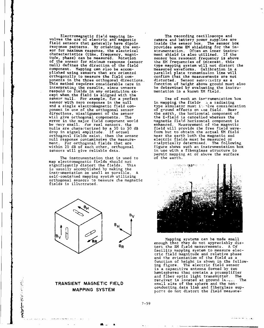
Electromagnetic field mapping in- The recording oscilloscope andvolves the use of electric and magnetic camera and battery power supplies arefield sensors that generally have dipole inside the sensor box. The sensor boxresronse patterns. By orienting the sen- provides some EM shielding for the in-sor for maximum response, the electrical strumentation, Often an inner instru-characteristics (time, frequency, magni- ment shield is also utilized. If thetude, phase) can be measured. Rotation sensor box resonant frequency is aboveof the sensor for minimum response (sensor the EM frequencies of interest, thisnull) defines the direction of the field type mapping system will not distort thecomponent. Mapping can also be accom- measured waveforms. Calibration in aplished using sensors that are oriented parallel plate transmission line willorthogonally to measure the field com- confirm that the measurements are notponents in the three orthogonal directions. distorted. Sensor sensi:ivity as aThis method requires considerable care in function of height above ground must alsointerpreting the results, since sensors be determined by evaluating the instru-respond to ?ields in any orientation ex- mentation in a known EM field.cept when the field is aligned with thesensor null. For example, for a perfect Use of such an inrsrumentation boxsensor with zero response in the null in mapping the fields .i a radiatingand a single electromagnetic field com- type simulator must i.YlIve considerationponent in one of the orthogonal sensor of ground effects on Lne field. Neardirections, misalignment of the sensor the earth, the horizontal component ofwiil give orthogonal components. The the E-field is cancelled whereas theerror in the major field component would magnetic field horizontal component isbe very small. for real sensors, the enhanced. Measurement of the magneticnulls are characterized by a 30 to 50 dB field will provide the free field wave-drop in signal amplitude. If actual form but to obtain the actual EM fieldorthogonal fields exist, then the sensor near the earth both the magnetic andnull response contaminates the measure- electric fields must be measured orment. For orthogonal fields that are analytically determined. The followingwithin 20 dB of each other, orthogonal figure shows such an instrumentation boxsensors will give reliable data. in use with a fiberglass structure to
permit mapping at or above the surfaceThe instrumentation that is used to of the earth.
map electromagnetic fields should notsignificantly distort the fields. Thisis usually accomplished by making theinstrumentation as small as possible. Aself-contained mapping system utilizingorthogonal sensors to measure che magneticfields is illuctrated.
BHB
B 8/Mapping systems can be made smallenough that they do not appreciably dis-
8 R tort the EM field measurements. A CWfacility mapping system to measure elec-tric field magnitude and relative phaseand the orientation of the field as afunction of height is shown in the follow-ing figure. The electric field sensoris a capacitive antenna formed by twohemispheres that contain a preamplifierand fiber optic light transmitter. Thereceiver is located at ground le-.-. The
'" TRANSIENT MAGNETIC FIELD small size of the sphere and the non-MAPN.YTMconductingdata link and fiberglass sup-MAPPING SYSTEM ports do not distort the field measure-4.
7-59
A a- ,4

ments. Field orientation is determined The reference side of the probe isby rotating the sphere to achieve a min- usually the ground or shield side of theimum response. probe output connector. For single-ended
probes, a ground terminal is availablenear the probe tip. A clip lead fromthis terminal to the circuit referencewill have an impedancea that is predomi-Gimbal Mount nantly inductive.
FrOpticThe reference for the voltage beingFiber Omeasured is defined by the location se-
lected to reference the probe.
Phenolic /With care, low-impedance, ten's ofSupport inanoseconds rise time voltages can be
measured directly. For high-impedanceReceiver and/or nanosecond rise times, the high-
frequency characteristics of the entirecircuit, probe -- return path systemmust be known.
CW ELECTRIC FIELD MAPPING SYSTEMCircuit Probe
Ideally, it is desirable to have atesting source that is not influenced bythe system being tested. For limited Circuit Referencesize sources, _t is often necessary toverify experimentally that this is, infact, the case. This measurement is a Referencepart of the source definition and requires Return Paththe same care and accuracy as the signalsource definition measurements.
A second application of these sensorsis for measurement of internal fields. The problem of signal or circuitThese same types of sensors can be used reference location makes it appealing toin this application, want to measure voltage directly beLween
two points in a circuit. This is a dif-ferential voltage measurement and differ-
Voltage Probes ential voltage probes are also commerciallyavailable.
Voltage, at a point within a system, A differential voltage probe is twois usually measured with a voltage probe. single-ended probes connected to givw anCommercial probes are available with rel- output that is the difference betweeTr theatively high input impedances (high re- two voltages. The difference is deter-sistance, small capacitance) that can have mined as the difference voltage on eachsubnanosecond response times. Often vol- probe tip referenced to the probe groundtage probes have attenuation from input or reference. Thus, the differentialto output. probe is a three-terminal network, and
if the probe reference is connected toThe actual response of any voltage the circuit, an inductive element is
probe is a function of the probe imped- again added to the measurement circuit.ances, the equivalent impedance of the If a reference lead is not used as anvoltage source being measured, and the attempt to eliminate this inductive ele-impedance of the circuit used co connect ment, then the probe reference and cir-the circuit reference and the probe refer- cuit reference will seek their ownence. The equivalent impedance of the unknown return path.voltage being measured is not always easyto define. Generally, voltages should be Since the probe is a three-terminalmeasured at low impedance locations in network, the voltage to be measured, V,circuits so that the probe will not load is shown as two voltage sources, V1 andor alter the voltage. V2 , in a three-terminal network. The
7-60
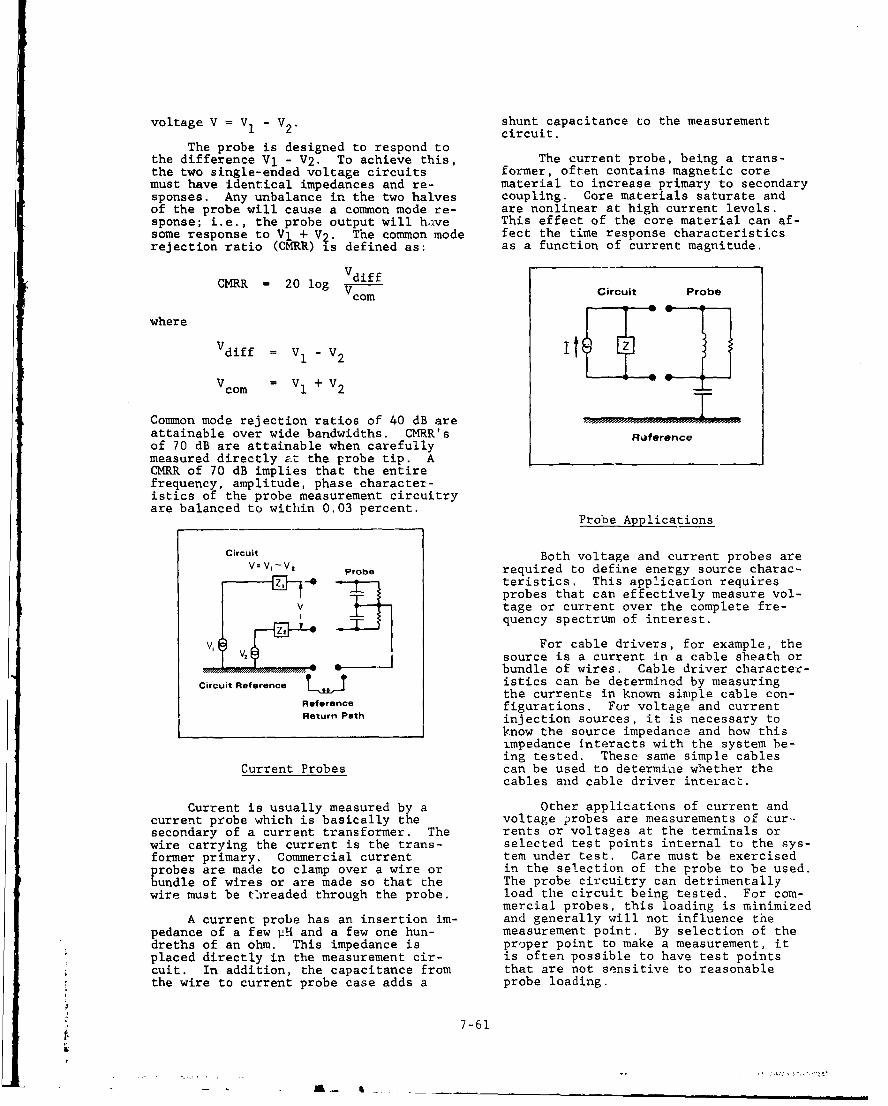
voltage V = V1 - V2 . shunt capacitance to the measurementcircuit.
The probe is designed to respond tothe difference V1 - V2. To achieve this, The current probe, being a trans-the two single-ended voltage circuits former, often contains magnetic coremust have identical impedances and re- material to increase primary to secondarysponses. Any unbalance in the two halves coupling. Core materials saturate andof the probe will cause a common mode re- are nonlinear at high current levels.sponse; i.e., the probe output will have This effect of the core material can af-some response to VI + V?. The common mode fect the time response characteristicsrejection ratio (CMRR) is defined as: as a function of current magnitude.
VdiffCMRR = 20 log Vcom Circuit Probe
where
Vdiff = V1 - V2
V com 1V V2
Common mode rejection ratios of 40 dB areattainable over wide bandwidths. CMRR's Referenceof 70 dB are attainable when carefullymeasured directly z.t the probe tip. ACMRR of 70 dB implies that the entirefrequency, amplitude, phase character-istics of the probe measurement circuitryare balanced to within 0.03 percent.
Probe Applications
Circuit Both voltage and current probes arev=v,-v, Probe required to define energy source charac-
teristics. This application requiresprobes that can effectively measure vol-
V' tage or current over the complete fre-quency spectrum of interest.
v1 For cable drivers, for example, theV2 source is a current in a cable sheath or
bundle of wires. Cable driver character-Circuit Reference istics can be determined by measuring
the currents in known simple cable con-Reference figurations. For voltage and currentReturn Path injection sources, it is necessary to
know the source impedance and how thisimpedance interacts with the system be-ing tested. These same simple cables
Current Probes can be used to determine whether thecables and cable driver interact.
Current is usually measured by a Other applications of current andcurrent probe which is basically the voltage probes are measurements of cur.-secondary of a current transformer. The rents or voltages at the terminals orwire carrying the current is the trans- selected test points internal to the sys-former primary. Commercial current tem under test. Care must be exercisedprobes are made to clamp over a wire or in the selection of the probe to be used.bundle of wires or are made so that the The probe circuitry can detrimentallywire must be t~ireaded through the probe. load the circuit being tested. For com-
mercial probes, this loading is minimizedA current probe has an insertion im- and generally will not influence the
pedance of a few vH and a few one hun- measurement point. By selection of thedreths of an ohm. This impedance is proper point to make a measurement, itplaced directly in the measurement cir- is often possible to have test pointscuit. In addition, the capacitance from that are not sensitive to reasonablethe wire to current probe case adds a probe loading.
7-61
t.
&A

Bulk cable currents generally can be Hardwire Data Linksmeasured with clamp-on probes on existingsystem cabling. If currents are to bemeasured within a shielded cable, it is One technique for coupling the sen-probably necessary to replace the system sors and probes to the recording systemcable with a special test cable. Such a is via hard wire cable. These cablestest cable is shown here with two current can be coaxial or twinaxial and single-probes under the cable shield. Shielding shielded or multiple-shielded. Mostintegrity can be determined in the labo- commercial probes terminate in a standardratory. transmission line coaxial cable. The
probes are designed for laboratory useand often will respond to electromagneticenergy via coupling into the probe casing.Thus it may be necessary to EMP hardenthe measurement system before the measure-ment system can be used in an EMP harden-ing program.
Shown is a hardened voltage probeintended for use with a recording systemthat is contained in a shielded container.Additional shielding in the form of braidhas been added. This additional shieldis connected to the probe at the sensorend.
Signal Distribution Systems
So far the discussion has centeredon measurement of the fields, voltages Termination Flangeand currents. The sensed signals mustbe transmitted to a recording system. To Probe Cable
accomplish this, some form of data trans-mission link must be provided. Often itis also necessary to condition the signal cast Metal Head
prior to recording. These factors arecombined into a single category - signal
Bri
distribution. Consequently, signal dis-tribution systems include: Another example, as illustrated, is
the hardening of a differential voltage
1. Cables such as coax, balanced or probe. A solid shield has been placedtwinax, shielded pair. around the probe which contains active
elements. In order to maintain a good
2. Nonconducting cables such as micro- CHRR, the cable has to be shielded withwave data links, dielectric wave- two layers of braid.guide, or fiber optics.
3 Amplifiers either wide bandwidthsor frequency selective.
4. Attenuators and signal dividers.
5. Signal conditioning to enhance ordepress either high-frequency,short-time or low-frequency, long-time response. T°,ndt....... Fl.ng.
Internal Signel Probe Heed
These are discussed in subsequent para- Ij~eC~i~
graphs of this section.
Prob. Head Shield
SBraidStd. Tinned Copper Braid
7-62
Ll?

A third example is a clamp-on typecurrent probe. This probe has a connector 0on the probe that is intended to be loaded RG-6/Uwith 50 ohms. Hardening of this probeinvolves shielding the probe to electro- -- 5./magnetic fields, selection of a signal R(,-58/Ucable (RG-55/U), and shielding the signal 80cable.
20 204)
3Ao0' 107 10' 109
Frequency-Hz
L in.0 Flange Nonconducting Data Links
55/u Internal Cable
----- d\ Nonconducting data links can be RFHeaid •ead Shio$d telemetry, dielectric-guided RF, or op-
tical. To be used effectively, the carri-er frequency of these data links must bewell above (a factor of ten or so) theEMP spec:rum. Segmented and loaded(lossy) transmission lines have limited
Shielding of signal cables is neces- bandwidth and are not commonly used.sary to eliminate response to unwantedelectromagnetic energies. These shieldsor the cable conductors themselves are RF Telemetrysensitive to electric fields along thecable. Interference can sometimes beminimized by repositioning of cables. How- An FF data link can take many forms.ever, cables in electromagnetic fields Commercial microwave data links are avail-alter the electromagnetic environment able that can be altered for broadbandand can alter the system EMP interaction, transient data transmission. Essentially,Ideally, cables should be routed away from such a data link consists of an energyother cables and should cross other sys- source, modulation from simple single-tem cables orthogonally to minimize coup- channel AM to multiple-channel FM-FM,ling to the system. Instrumernt: cables directional antennas (usually a horn), ashould be routed adjacent to conducting receiver, and a demodulator. Power inskins or cabinets to minimize loop cur- the form of batteries must be suppliedrents in the cables. Cables should never at the transmission end of the link.be allowed to dangle across open areas Thus, the physical size of the instru-where they can alter the EM environment. mentation that must be added to the
probes can overcome any advantage ofHardwire cabling systems also ex- the nonconducting data link.
hibit attenuation or delay characteristicswhich are a function of frequency. Illus-trated are the amplitude attenuation Dats Inputscharacteristics for RG/58/U and RG-8/Ucoaxial cables. The usable bandwidth(-3 dB points) for these cables are 25 Modultor Transmitter
MHz and 150 MHz, respectively. For broad-band signals these characteristics mustbe known and accounted for in the process- Power Antenna
ing of the data or by frequency compen-sating the cables. Synthesis codes havebeen developed to equalize the cable Antennaresponse, usually at the expense of in-creased attenuation as shown by the dashed emodultor verline. Equalization must be accomplishedfor both attenuation and phase if goodresponse of the cable is to be achieved. Doet Outputs
7-63
ML!

This form of data transmission re- ivs output being directly proportionalquires radiation of an RF signal. If the to the current through it. The trans-RF signal is within the EMP spectrum, the mission link can be lens and mirrors;radiated (simulator) field will interfere however, mechanical alignment limitswith, and may even mask, the telemetered their field application. Light can easi-data. Choosing a telemetry frequency far ly be transmitted using flexible fiberabove (ten times the highest frequency optics. The size of an optical datain the EMP spectrum), low pass filtering transmitter can be quite small, Opticalcan be employed to eliminate this inter- links with bandwidths up to 150 MHz areference problem. commercially available with relatively
low loss.The radiated RF telemetry signal can
also interfere with the measurement of theradiated EMP tields. For example, if theEMP field sensors have a very broad band--~''width, they may respond to the telemetrysignal resulting in distortion of the or S r
measured EMP fields. ' :-Pream Ap Pwr Emi~ttng
Amp LDrop. IThe physical size of the probe end FirOptiL k
of the data link can be reduced if power,. his supplied from the receiver end of the onipet •Rec.p..-link. This may be accomplished by pro- A-ip i tc, proi__ - o-op.viding the RF power from the receiver endvia a second channel (as illustrated) or * ,y•-Ar.two way propagation on a signal channel. Output lt""•e .
SDielectric Weveguirle A ne
Da. ModualtoirInputs Signal Conditioning
Amplifiers
Amplifiers for pulse or transient[4ro r . .application have a constant gain and
linear phase response over a broad rangeDat. Outpit. of frequencies defined as the amplifier
bandwidth. For linear phase response,the phase delay increases linearly with
Dielectric Waveguide Transmission frequency. This is equivalent to a con-stant time delay for all frequencies
The use of dielectric waveguide, il- which results in no dispersion or phasedistortion of a time waveform. Outsidelustrated above, eliminates the need for the amplifier bandwidth, amplitude willradiating antennas. Energy propagates tampifr and phase willboth within and on the rod surface in a vary with frequency and phase will dexi-transverse magnetic mode and may extend ate from linear phase. This causes pulse1 to 6 inches beyond the surface depend- disLortion in an amplifier.ing on the frequency and dielectric mater-ial. Thus, some protection is requiredto keep conductors away from the rod.Propagation losses less than 0.1 dB/ft. dwidth---,have been measured at 12, 24 and 48 GHz. dDirt on the rod surface can increase thisloss,
Dielectric rod transmission systemsheve been successfully used at Ku (12 to1.8 GRz) and X (8 to 12 GHz) band frequen-cies with rod sections in excess of 100 Efeet. Bending of the rod on a 10 footradius does not noticeably affect systemperformance. I
Freq .ency
Optical Transmission
Data can also be transmitted by modu-lating light. The light-emitting diodeoffers an easy method to modulace light,
7-64

Both the low-frequency cutoff andhigh-frequency cutoff characteristics areimportant. These cutoff frequencies aredetermined by the RC time constants assoc-iated with the amplifier circuit. Phase e e- Ideal
The high-frequency response of the ....-----
amplifier limits the rise time of the out- -put waveform. The rise of the output wave- 8-4 Typicalform is exponential. Tf the time constant(12) associated with the high-.frequencycutoff is less than five (5) times therise time (ti) of the input pulse, theerror introduced will be less than one fO fcl f Frequency(1) percent. The high-frequency responsealso contrnls the decay of the pulsewhich will also be exponential. Inade-quate high-frequency response will resultin a reduction in the output pulse ampli-tude.
The low-frequency response of theamplifier results in a sag in the top ofthe pulse (output voltage dropping dueto changing of the capacitance associatedwizh the output coupling circuit). Thiseffect is seen primarily for long pulses, The effects of the high and low-fre-(i.e.. where the pulse ..ation is long quency cutoff characteristics of an ampli-compared to the RC time -jnstant of the fier are depicted qualitatively in theoutput circuit). The low-frequency re- following figure. The figure indicatessponse also results in overshoot at the the pulse droop or sag due to'the ampli-end of the pulse due to this charging of fiers low-frequency cutoff and the de-the coupling capacitance. graded rise time of the output pulse due
to the amplifiers high-frequency cutoff.
4Pulse Drop
g* Ideal Characteristic - -P--lenput Pulse
V W .ý-Output Pulse
Typical Chara:teristlc E \
fc f -- •" '•lR Time----
In addition to the amplitude response, The low-frequency and high-frequencydistortion of the cutput pulse can also cutoffs do not amply define the responseresult from non-linear phase delay of the of a broadband amplifier, since the rela-amplifier. The phase delay distortion for tive amplitude and phase of signal spec-the first-distortion terms in the Fourier tral components outside these limitsrepresentation are shown in the figure. affect the amplifier response. ShownThe dotted line shows the ideal character- in the figure is the ideal amplifieristic (linear phase delay with frequency) amplitude response characteristics (dottedand the solid line the sinusoidal devia- line) and the typical pulse responsetion from the tdeal. (solid line).
7-65

The effect on the output pulse shape the stray capacitance associated with thefor a square wave input pulse is shown output (C2 ) will alter the attenuationin the following figure. Figure (a) shows ratio. Its effect can be compensated bythe distortion due to he amplitude re- the addition of Cl in the compensatedsponse only, and Figure (b) includes the attenuator shown. Compensation requiredeffects of phase distortion. to maintain the desired attenuation ratio
is given by RIC1 - R2C2.
C,,R,
IIn I
-T 0 T
Time For still higher frequencies, allA.) AMPLITUDE RESPONSE lumped components have R,C, and L. In
addition, the voltage source will havea source impedance and the load a loadimpedance. The effects of all these im-pedances must be considered when design-irg high frequency broadband attenuators.Any attenuator, no matter how complicatedits compensation may be, has some usefullimited frequency range or bandwidth.
Without PhaseI/DistortioTo
Time ---- Distortion
B.) EFFECTS OF PHASE RESPONSE ZL
Amplification of CW signals can takea variety of forms. These can includesimple straightforward amplification with Signal Dividersbandwidth-limiting filters to reducenoise. 7requency translation can be usedbut must be done coherently to preserve Often, between the sensor or probephase. Detection of amplitude and phase and data recorder, the signal is distri-of the signal require coherent detection buted either to multiple recorders or tothat can be accomplished with synchronous perform other functions, such as trigger-detectors in phase quadrature. ing an oscilloscope. These functions
must be accomplished without distortingthe signal c'hannel. Signal energy for
Attenuators triggering can be obtained with a highimpedance tap off whose impedance is muchlarger than the signal channel imnpedance.
The concept of attenuation is a Signal distribution is normally accom-simple one. If two resistors are con- plisbed with a signal divider that hasnected, as s1hown on the left, then the an input impedance that matchei the sig-output voltage is attenuated by R2/Rl + nal line impedance and gentrally willR2 from the input voltage. If the resis- have individual output impedances match-tance values are not too large and fre- ing the output line impedances. Passivequency in low, this form of attenuation circuits that have constant input andis valid. output impedances have isolation oetween
input and output in the form of loss orHowever, as frequency is increased, signal attenuation.
7-66
A

For broadband applications, fc mustbe well outside the signal spectrum, In
s~gn, •Trigger 0 addition, the effects of source and loadimpedance and distributed impedances willlimit the useful frequency range of atrue integrating or differentiating cir-cuit.
signal
0 Hgh as
Impedance mismatches cause reflec- Lewtions in the signal channel. For CW, thereflections result in a voltage standing-wave ratio (VSWR). A VSWR of 1.5, whichis considered adequate for some applica-tions, corresponds to a voltage reflec-tion of 20 percent. As indicated here,a 20 percent reflection can result in Other forms of special filters mayconsiderable distortion of a transient. be used either to enhance a frequency or
frequency band or to attenuate a dis-One technique that is useful to de- crete frequency or frequency band (notch
fine and locate reflections in a signal filter). Such techniques should be usedchannel is time-domain reflectometry. with caution since phase as well as ampli-Commercial TDR's are readily available tude are altered over a frequency rangewith subnanosecond accuracies, that is the filter bandwidth.
VSWR1 1.8:1 Q_____
Reflection is 20.7070 f_
0
Differentiators and Integrato':s- 90°
Sometimes it is desirable to distortthe signal spectrum intentionally. Dif- Signal Display and Recordingferentiation of the signal will enhancethe high-frequency response or result ina signal that is the time derivative. Dif- Recording of transients in the timeferentiation can improve time definition, domain is normally done using an oscillo-A differentiator has an amplitude response scope and film. A single recording orthat is directly proportional to frequen- multiple recordings to extend dynamiccy. A singie-stage high-pass filter shown range may be used. Transient recordingin the upper part of the figure has an can be digital or a simple peak magni-amplitude response variation of 6 dB per tude recording.octave below the cutoff frequency, fc.Thus, for frequencies below fc, the out- CW is usually recorded on chartput is the differential cf the input, recorders that can be simple time-ampli-Similarly, a low-pass filter with 6 dB tude recordings of x-y plots. Often the
ýJ per octave roll off will integrate all recording of a meter deflection will suf-frequencies above f fice.
7-67
*1'

Oscillosccpe/Camara Recording measurable frequency chat is recorded.Thus, 300 tracewidths limit the recordedbandwidth to a maximum of 30 to 1.
In spite of recent developments inalternative recording techniques, the best A 150-MHz oscilloscope set to recordinstrument for recording a transient is ],50 MHz will not display frequencies be-still the oscilloscope-camera combination. low about 5 MHz. If the sweep speed isOscilloscopes ,.re normally specified as set to record 10 kHz, then the maximumto bandwidth, deflection sensitivity, observable frequency is less than 1 MHz,sweep time, and writing rate. These param- even though the oscilloscope is capableeters define an oscilloscope but do not of responding to 150 MHz.define its capability to display transientdata.
For the display of transient data, Typical Oscilloscope Displayit is convenient to define the oscillo-scope capabilities in terms of the displayspot size. The time response of the os- Icilloscope cepends upon sensitivity involts per spot width and the slewing rate Iin deflection per unit time. Slewin:r . rate todepends on oscilloscope writing rate andupon the volts per second capability of •j jj ij'the amplifiers. Resolution ias defined inthe number of tracewidths that can be dis- 300played. The tracewidth is the minimum -Tracewidths ewidth of the trace of an oscilloscope.
OSCILLOSCOPES
SPECIFICATIONS A single oscilloscope recording is"* BANDWIDTH very limited itt its amplitude and time
dynamic range. Usually, to record tran-"* DEFLECTION SENSITIVITY sients associated with EMP hardness test-ing, more than one recording of each
"* SWEEP SPEEDS waveform is required. The recording dy-namic range sets a time-amplitude window
"* WRITING RATE that can be recorded. Four such typicalwindows are shown here as the solid lines.
tRANSIENT RECORD!NG The upper end of each line represents thefull-scale deflection voltage and the
* StOV SIZE sweep length. The lower end of each lineis the voltage and time resolution for
, SENSITIVITY the particular oscilloscope settings.
* SLEWING RATE The dashed line represents a rapidsweep recording that has been initiated* RESOLUTION at a later time by a delayed trigger.
This technique Dermits good time defini-Typically, the vertical deflection is tion at latter times in the transient wave-
limited to about 200 tracewidths. This form.number of tracewidths limits the dynamicrange to a maximum of 46 dB, providingthat & change of one tracewidth is observ- -o_
able in data reduction.
The recorded bandwidth is determined Iby the number of tracewidths alcng the '-time axis, typically 300, and the sweepduration. A theoretical. limit of defini-/nition five times this minimum samplingrate is desirable; i.e., 10 tracewid~hs /per cycle. Thus, for an oscilloscope with300 tracewidths per sweep, a sweep speedcan be selected to display 30 cycles of ,o" , .°the highest frequency to be displayed. TneSSco"ds
This length of sweep will display onecycle of a frequency that is 1/30 of thehighest frequency, which is the lowest
7-68

To display a waveform on an oscillo- A.izghtly less than the period betweenscope requires that the oscilloscope sweep pulses.and the waveform be aligned in time bytriggering the sweep at a known time with For transient recording, the triggerrespect to the waveform. Triggering can can be derived from the fields that im-be derived from the waveform, thus start- pinge on the system or from the senseding the sweep after the waveform onset, simulator field. Fither of these methodsIt is important to realize that, if the can contaminate the measurement itself.o'cilloscope sweep is nonlinear, it is Extreme care must be used to ensure thatprobably nonlinear at the sweep onset. there are no unwanted EMF penetrationsThus, with self-triggering, the initial into the measurement system.portion of the waveform is lost and maypossibly be distorted.
Self-Triggering External Trigger
Trigger Level _
Way~form Measurement System DIspleY
Ospilloscope Displev
The recording of a waveform or tran-sient on film is dependent upon manyfactors. Trace recording is ideally linephotography, so that overexposure of thefilm seems to be desirable. However,
This problem can be overcome by add- the oscilloscope trace has a Gaussianing delay to the signal channel that is distribution that will cause the :race tonot in the trigger circuit. Many oscillo- broaden as trace intensity is inc.-eased.scopes have internal delay for this pur- The effects of high intensity are iot al-pose. However, the signal distortion ways obvious to the eye since the eyecharacteristics of broadband delay lines responds logarithmically over a millior-must be included in the overall measure- to-one range, while film responds linearlyment system response. Delay of a few over a 100-to-one range.ten's of nanoseconds can be obtained us-ing good coaxial cable. Most oscilloscope cameras will have
at least an f 1.9 lens with a slightimage reduction (magnification = 0.85).The most common phosphor for the oscillo-
ant' scope is P-31, which is optimized forMeasurement Delay splay visual use, Other phosphors, P-11 forSystem 1 -T example, are better matched to films that
are sensitive generally to blues.
Sweep
Trigger >
CircuitC P11 1I0 3
An alternate method of aligning the .2waveform and oscilloscope trace is toprovide an independent trigger to initi-
ate the sweep prior to the waveform. For >2o 0040 0•5 • crepetitive pulse applications, this trig-3540405050 L657Cger source can be the waveform itself with Wavelength
delay in the trigger channel that is
7-69

The film writing speed is a function the oscilloscope sweep is not objection-of many factors. These factors include: able.
* Oscilloscope tube phosphor The improvement in sensitivity thatis possible by using CW and narrowband
* Development time filters can be utilized to display re-petitive pulse measurements. Current
9 Film speed state-of-the-art sampling techniques havebeen utilized with standard oscilloscopes
* Lens f number (speed) to display sine waves about 10 GHz andrepetitive pulse rin times in the ten's
• Film pre-processing of picoseconds (10- " seconds).
The increase in writing speed that can be Sampling is a process wherein aobtained by proper choice of these factors narrow-time gate is used to measure andis shown in the figure. store the input signal that occurs at
the time of the sample. By moving thesample gate along the waveform on sub-
64x Vogg9ng sequent repeated waveforms, the entirewaveform is sampled, stored, and dis-
C3x .tL,,., .2/Mag .05 played. Sampling at each point on thet waveform is normally a single sample;
however, multiple samples are possible so2 '" that averaging can be used to improve
E ax o.o00ASA signal-to-noise ratios.
4X/ 2 Sec. Development Analog/Digital Recording
2X P p1 Phosphor
Analog recording of a transient can0 Ref.ence - f 1.9/M•O 0 Z.35 3000 ASA be accomplished on tape recorders or on
magnetic discs. Bandwidths of ten's ofmegahertz are feasible. However, tapeor magnetic recorders have poor signal-to-noise ratios, limiting their dynamicrange to about 30 dB. Linearity through
The exact form of film and camera playback can be adequate with proper cali-that is used will depend upon the data bration. The overload characteristicsinterpretation process that is used with of tape usually demonstrate poor recovery.the test program. Polaroid cameras andfilm give an instant permanent record. Various methods are available toThe recording can be viewed to determine record transient waveforms in digitalif it is reidable and if additional form. The building blocks are availablerecords are required. This feature elim- in various forms so that particular sys-inates the recording of useless data. The tems can be assembled for specific appli-disadvantage of Polaroid film is that it cations.is difficult to use in machine processingincluding viewers and only a single copy Generally, digital recording involves(print) is available. Polaroid does make analog storage to permit waveform samp-a negative film intenaed for use in mak- ling, analog-to-digital conversion ofing slides; however, the speed of this amplitude, conversion of the time scale,film limits its usefulness in transient intermediate or temporary storage betweenrecording. the time and at,)litude conversion pro-
cesses, and finally, storage of the digi-The Polaroid camera is essentially tal information. The most common version
a framing camera where the film can be of digital :ecording is shown in thepositioned for multiple exposures if de- upper diagram. The analog signal issired. Framing cameras exist for stan- stored in some manner so that time samplesdard films, usually 4 x 5 inches. can be determined (usually at a nonreal
time) and then each sample is digitizedFor measurements that are repeated and stored. The time conversion permits
many times, a stepping camera is useful. the analog-to-digital conversion to beStepping cameras are usually 35 mm and accomplished at a lower bit rate.automatically stepped one frame at a time.The film is continuous. An alternate approach is shown in
the lower diagram where the analog-to-Continuous motion cameras can be digital conversion is accomplished first.
used similar to a stepping camera, pro- Time conversion is then accomplished onviding the film motion distortion during the digital data. This technique is
7-70
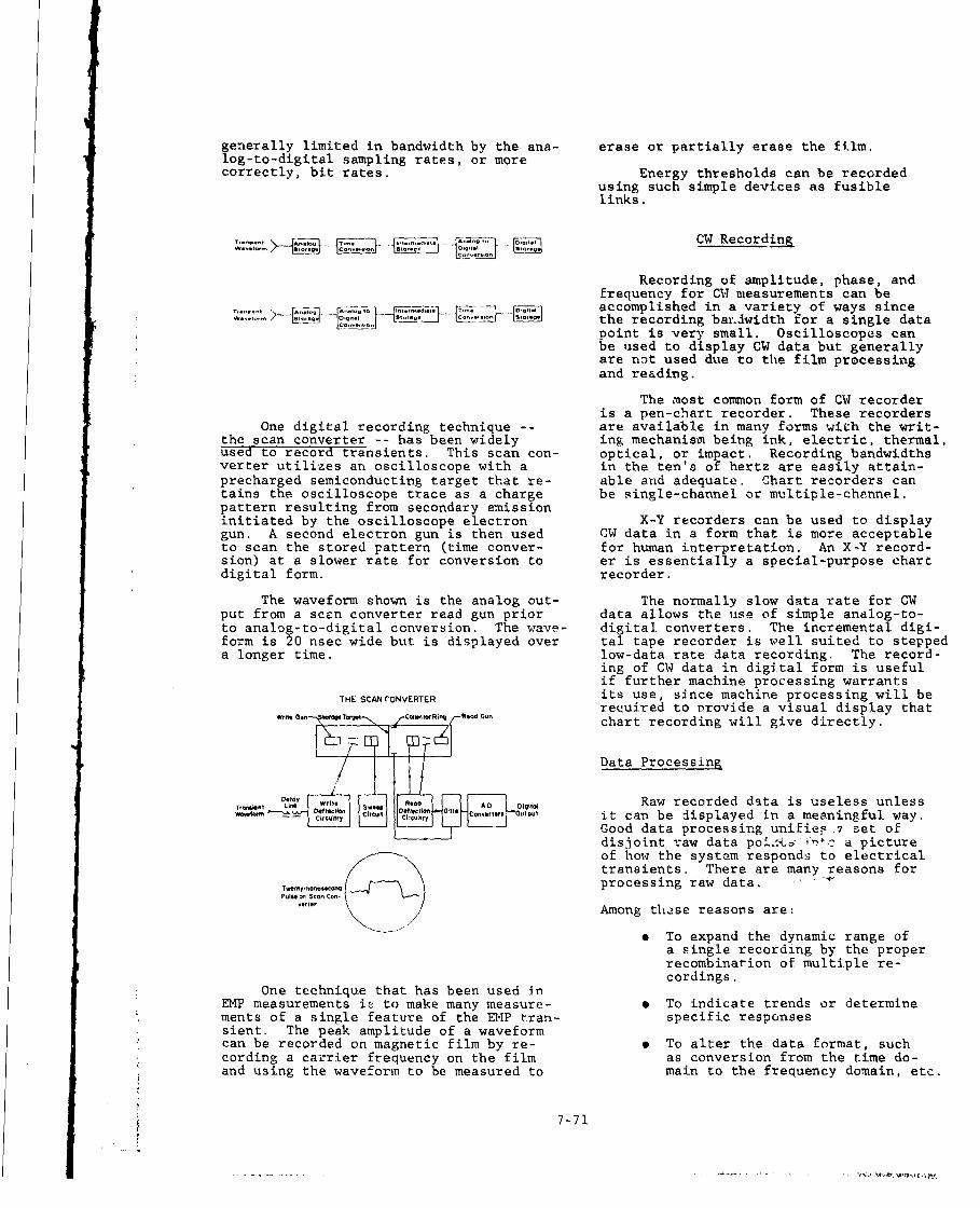
generally limited in bandwidth by the ana- erase or partially erase the film.log-to-digital sampling rates, or morecorrectly, bit rates. Energy thresholds can be recorded
using such simple devices as fusiblelinks.
f-7-~- ~m zr CW Recording
Recording of amplitude, phase, andfrequency for CVW measurements can be
S q ,.. •,. • --....... accomplished in a variety of ways since-- l F c.-! I the recording bart.width for a single data
point is very small. Oscilloscopes canbe used to display CW data but generallyare not used due to the film processingand reading.
The most comnmon form of CW recorderis a pen-chart recorder. These recorders
One digital recording technique -- are available in many forms with the writ-the scan converter -- has been widely ing mechanism being ink, electric, thermal,used to record transients. This scan con- optical, or impact. Recording bandwidthsverter utilizes an oscilloscope with a in the ten's of hertz are easily attain-precharged semiconducting target that re- able and adequate. Chart recorders cantains the oscilloscope trace as a charge be single-channel or multiple-channel.pattern resulting from secondary emissioninitiated by the oscilloscope electron X-Y recorders can be used to displaygun. A second electron gun is then used CW data in a form that is more acceptableto scan the stored pattern (time conver- for human interpretation. An X-Y record-sion) at a slower rate for conversion to er is essentially a special-purpose chartdigital form. recorder.
The waveform shown is the analog out- The normally slow data rate for CWput from a scan converter read gun prior data allows the use of simple analog-to-to analog-to-digital conversion. The wave- digital converters. The incremental digi-form is 20 nsec wide but is displayed over tal tape recorder is well suited to steppeda longer time. low-data rate data recording. The record-
ing of CW data in digital form is usefulif further machine processing warrants
THE SCAN CONVERTER its use, since machine processing will bereeuired to nrovide a visual display that
-ri% Gwo,,t CawRing / chart recording will give directly.
Data Processing
Trwal L R.od Raw recorded data is useless unlessD ~rfA 00401-0on
circu _ y • fltro, it can be displayed in a meaningful way.Good data processing unifie- . set ofdisjoint raw data poi*. c i' a pictureof how the system responds to electricaltransients. There are many reasons for
Tý n Can-, processing raw data.
Among the3se reasons are:
* To expand the dynamic range ofa single recording by the properrecombination of multiple re-cordings.
One technique that has been used inEMP measurements it to make many measure- * To indicate trends or determinements of a single feature of the EMP tran- specific responsessient. The peak amplitude of a waveformcan be recorded on magnetic film by re- 9 To alter the data format, suchcording a carrier frequency on the film as conversion from the time do-and using the waveform to be measured to main to the frequency domain, etc.
7-71

9 To average or summarize the re- Calibrationsuits from a number of discretetests to minimize measurementerrors Proper calibration necessitates a
complete understanding of the response* To compare data characteristics of the entire measure-
ment system. For transient recordings,9 To average out noise, the transient or pulse response of the
system must be measured and documented;There arc a wide variety of tech- and for CW measurements, the freqi•pncy
niques or machines to perform these data vs. amplitude and sometimes vs. phasereduction or processing functions. In must be measured and documented. Thesesome instances, where only a limited calibrations must be periodically veri-amount of data must be processed or where fied.only a "quick look" is desired, the pro-cessing may be accomplished manually. Calibration signals should be in-Manual processing may include manual digi- cluded with the data to be certain thattization of oscillograms, etc. Where recurded amplitudes, times, and frequen-large volumes of data must be processed cies are correct. Calibrations shouldor where a great deal of manipulation of be an integral part of the entite datathe data is required, manual processing measurement procedure including the datais impractical and machine processing reduction system. Recorded data is use-must be employed. A few typical cate- less unless the relationship between thegories of machines for this purpose are signal being sensed and the tabulated orindicated, displayed data is known.
Calibrations determine overall re-7 sponse characteristics, relate inputs to
Processing Machines outputs, and provide scale factors forthe data. In practice, measurement sys-tems calibrations are accomplished in
Analog-to-digital scalers three steps: in-the-field measurementsystem calibration, data record calibia-
SIBM card systems tions and data processing calibration.
Calibration, ideally, should only*Plotters have to be performed at the onset of the
test program. This would be acceptable*Special-purpose computers if the simulator output, and the measure-
ment system responoe did not change with*General-purpose computers time. In some cases, changes have been
seen to occur from shot to shot. There-fore, periodic checks are required. Thefrequency at which the calibration must">e repeated is a function of the perform-
Where machine processing is required, ance of the energy source and the measure-the necessary programs must be available. ment system. This repeatability of dataSome of the more commonly used are indi- must be determined prior to t'ie actualcated. Special programs may have to be test program.developed depending on the type of data,data format, or information output de-. Factors which cause instrumentationsired from the data. A great many special system calibration to change include:programs exist but are not listed sincethey generally are not applicable. 9 Carelessness resulting in damage
to the instruments or telemetry
Mathematical Tools links.
9 Misalignment or improper con-nec'tion of telemetry links
xTime Domain Conversion e Temperature effects
S Aging of components or batteries
S$tatistical used in remote units
e Rerouting of cabling and changingECircuit Analysis length of telemetry cables
* Replacement of signal wires or
*Special-Purposec
7-72

Many of these factors are long-term main- longest observable time limit of thetenance problems. Others, such as battery system determined from the system low-charge conditions, may change over short frequency response. An impulse must haveperiods on the order of 2 to 4 hours. a total duration that does not exceed 1/10Again, depending on the known performance the measurement time response or risecharecteristics and condition of the sys- time. These requirements on the waveformtem, the frequency of calibration checks used to determine system response meanscan be established, that the waveform spectrum exceeds the
measurement system bandwidth. Observa-tion of these input waveforms requires
Measurement System Calibration the use of even wider bandwidth oscillo-scopes. For repetitive pulses, widerbandwidths can usually be recorded using
The measurement of the in-the-field such techniques as a sampling oscillo-system performance involves exposing the scope.measurement system to a known signal andrecording the resulting output signal. The system transient response measure-For probes, known voltages and currents menL demands that multiple records of thecan be directly coupled to the probes. measurement system output be made with aFor a field sensor measurement system, wide range of amplitudes and time basesthe entire system must be exposed to a so that the output time history can beknown electromagnetic field. This often accurately defined. Definition of theis done using a transmission line simu- measurement system pulse response meanslator as discussed earlier. If a probe that the system time response is definedmeasurement system is to be used in the for all times, both fast rise times andpresence of large simulated EMP electro- long decay times. The response must bemagnetic fields, then that system response measured at a sufficient number of timeto the incident fields must be known. points so that straight lines between the
points still define the waveform. Often,The impulse response or CW amplitude over 1000 points are required to define
and phase response can be used to define each waveform accurately.system measurement characteristics since,for linear systems, the impulse response The time responsý of a system canis the inverse Fourier transform of the be measured using any other input wave-CW amplitude and phase response. If the shape, provided the waveshape is accur-CW response is to be used to unfold time ately known and its spectrum is well knownhistory recordings, response data is re- over a bandwidth that exceeds the measure-quired to define amplitudes that are down ment system bandwidth. The tesponse ofat least 40 dB from the maximum or mid- a system can never be defined by a test-band response. Phase must be defined at ing spectrum that only partially coverseach frequencv. Phase measurements must the system bandwidth.be made at a minimum of five frequenciesper cycle of system phase response Repetitive pulses with known spec-(0 < ý < R radians). Both the phase and tral notches or amplitude zeros shouldamplitude must be measured at all fre- not be used to determine system responsequencies. because of the obvious problems associated
with division by a vanishingly small num-The accurate measurement of phase ber.
using an oscilloscope to record the datais difficult. Determination of the zerocrossing or specified amplitude level on Data Re'cording System Calibrationsuccessive cycles from the oscillogramscan easily result in errors due to manualdata reduction. Also, low-level CW signal An in-the-field measurement systemresponse cannot be used to determine designed to record waveforms whose re-measurement system overload response which sponse is well known is useless if theis a function of signal amplitude and is system produces unmarked, unlabeled photo-a nonlinear process, graphs or charts. Data calibrations must
accompany each record so that each pointPulse or transient measurements can of the record can be assigned a value
be used to determine system response. The that can be related to the sensed signalsCep function response and/or impulse re- using the known measurement system re-sponse can be measured, providing suffi- sponse. Most receiving and recordingcient care and accuracy are used to make systems wil! have nonlinearities whichthe measurements. A step function input must be calibrated even though the sys-must rise in a time that is at least an tem may be reasonably linear in the regionorder of magnitude faster than the re- in which it is intended to be used.sponse rise time of the measurement sys-tem, and must remain at constant amplitude Waveform calibrations required in-for a time that is long compared to the elude a standard time waveform. A CW
7-73

signal is often used for a time reference, can be related directly to the measuredCW frequencies that are above the normal signal. If calibrations are injectedsystem bandwidth must be used to adequate- at any other point in the measuremently quantify short times. Frequency can system, then the system response cali-be accurately measured to determine time. brations must also include the calibra-
tion system response.Amplitude calibrations can take the
form of volts-per-unit deflection or can Amplitude calibration is usuallybe applied at the measurement system sen- performed using a signal with a fixedsor or probe to give directly the sensed known phase. Phase calibration is per-parametet-per-unit deflection. If a fast- formed with a known constant amplituderise, flat-topped pulse is used for wave- signal. The system phase response mayform calibration, care must be exercised be a function of amplitude, thus requir-to select an amplitude point on the cali- ing additional data calibrations withbration waveform where the system loss is several signals of different amplitudes.well known to calibrate the data displayin terms of volts/division or other para- The calibration signal must be pre-meters since pulse distortion may be pre- cisely located in frequency relative tosent. A CW signal within the system- the frequency characteristics of theresponse bandwidth can be used to allevi- measurement system. For relatively broad-ate this problem. However, a single fre- band systems, this is simple. However,quency does not verify that the waveform if the system has a very narrow bandwidth,system response is unaltered. It seems it may be necesbary to provide withindesirable to use some combination of the system some method whereby the cali-pulse and CW for calibrations. bration signal and system tuning fre-
quency can be aligned by zero-beating,Regardless of the type of amplitude for example. In all cases, the data
calibration that is used, more than one records require an indication of systemamplitude is required to check for non- frequency and calibration signal fre-linearities. Just as important, it is quency.necessary to know zero level for all read-ings since amplitude is a linear measure- For CW data recordings as with allment from some reference (zero) to the data recordings, zeros of amplitude andpoint on the waveform, phase must be included in the data cali-
brations. Since normally more than oneWaveforms that have both rapid and recorder is required to record amplitude,
long-time variations are often recorded phase, and frequency, some common refer-on multiple records. The assembling of ence to all recordings is required. Forthese records into a single waveform single-drive, multiple-recording channelrecord requires that overlapping features recorders, the known relative positionsof the individual records be matched -- of the various recording pens suffice.usually in time. Waveform features that For multiple recorders, a common refer-are well defined can be used but often do ence signal and "side marking" pens arenot exist where wanted. Thus, some commonly used. As with any recordingcommon time reference is desirable for system, housekeeping functions must bemultiple recordings. Trace intensity modu- recorded to define the measurement andlation can be used for this function. A the measurement system.calibrated waveform also requires labelsto define the measurement parameters thatare not a part of the measurement system. Data Processing System CalibrationThese housekeeping parameters are testpoint location, date of measurement andother parameters that relate the data to Knowing the in-the-field measurementthe EMP hardness test plan. Often in- system response characteristics and havingcluded are measurement system parameters, well marked and calibrated data recordssuch as control settings, that can be are necessary but are not sufficient toused to verify the calibrations or 3ome- a good test program. The response char-times in place of waveform calibrations. acteristics of the data pi-zcsing sys-The redundancy in housekeeping records tem must be known since processingcan resolve human errors in the data. translates the recorded data into a mean-
ingful format.Measurement systems that record data
in the frequency domain must also provide Even the simple processing that iscalibrated records. Both the amplitude involved in hand plotting of data willand phase result in some form of recording alter the dynamic range and reading sensi-deflection. Each recording requires tivity.calibration. For amplitude-phase cali-brations, it is often desirable to inject Processing calibrations must be madethe calibration signal at the sensor or for time base translation, time-to-fre-probe so that both amplitude and phase quency translation, for frequency trans-
7-74
aL

lation, frequency-to-time translation, worst-case orientation. If a worst-caseand for amplitude trarslation. Linearity, orientation can be found, then all sub-dynamic range, and sensitivity must be sequent testing can be accomplished atdetermined, that orientation. Predicted worst-case
orientations should always be experiment-Data processing is an information ally verified.
filter and, as such, can only lose infor-mation. Information is lost in process- The operational modes of the systeming errors. Processing errors can come can also effect its response. Therefore,from machine and human error or from in- verification of predicted worst-casecorrect or inadequate mathematical pro- operational modes is required. Generally,cesses. The processing of representative to determine the worst-case operationalsample data or sample problems will veri- mode involves functional testing or dam-fy calibration of the processing tools, age testing.
Critical point testing is the experi-Test Instrumentation Setup mental determination or verification of
the critical points in the system. Twotypes of tests are used. One is an in-
Many instrumentation concepts have ternal mapping of signals at the variousbeen presented for use in an EMP test entry points to determine those areasprogram. The implementation of these within the system that give maximum re-techniques, some of the precautions that sponse to EMP fields. Initially, suchmust be taken when implemencing these mapping can be accomplished with quickconcepts, and approaches to insure the looks at the data to rank-order the ob-data obtained is reliable and valid servations. This rank-ordering can oftenare discussed in this section. be done with a visual observation.
The other procedure for locatingTesting Requirements critical points is to test portions of
the system in the laboratory and observedamage or upset. The mating of these
System hardness testing requires the two experimental approaches defines theuse of simulators to create EM fields, system critical points.The measurement of these fields over thetest area (mapping) must be done with Point-of-entry testing provides in-care. The test instrumaentation must be formation and definition of the coupledchecked for noise immunity. Further, the signals to critical portions of the sys-instrumentation must not influence the tem. Component ceamage and impact testingresponse of the system under test, It is is commonly accomplished or based uponnot always easy to differentiate between the energy content in a square pulse.valid data and noise. Because many components are sensitive to
waveform power spectra and polarity re-The system that is under test must versals, it is preferable to use waveforms
be exercised for all operational modes which more accurately approximate theand configurations. The operational per- actual signals measured during the point-formance of the system must be ascertained of-entry testing.before, during and after the test. Testconfigurations include system orientationin the EMP field, and determination of Test Point Accessibilitypoints of entry into the system.
In the early stages of a test pro- The critical points in a system thatgram, the experimental determination of must be monitored in a test program arethe orientation and operational mode that often internal to the system in a packagegives the maximum EMP interaction with that has limited space and access. Thus,the system is required. to make'measurements at these locations,
some modifications must be made to theDuring the test planning stage, the system. The use of circuit extenders is
various portions of the system must be one technique employed for voltage measure-reviewed to determine the electromagnetic ments at hard-to-get-at critical points.response of the system. Each portion of However, the addition of extenders re-the system will have a maximum response quirss space that is not always available.for some specific orientation of theapplied electromagnetic field. This maxi- Limited space in a system often re-mum will not necessarily occur on all quires that the recording instrumentationportions of the system at one particular be remote from the measurement point.field orientation. Thus, it is often With or without the use of adaptors, itnecessary to determine experimentally if is often necessary to cable the measureda particular field orientation is the data to a location that is accessible
7-75

during testing. Such a location could be Sometimes space within the systema connector panel that is located in an can be found for the measurement systemindividual equipment case or cabinet or by removal of some noncritical portioncan be on the external surface of the of the system. The most obvious placesystem. The routing of the cables and to find space is in some non-electro-the shielding integrity of the connector magnetic portion of the system such aspanel should be accomplished in such a a rocket motor bottle, for example.way as to minimize their effects on sys-tem performance during testing.
The recording system or nonconduct-ing data transmission system can be at-tached to a cable connector panel by Te.tusing a shielded enclosure as illustrated. EquipmentThe instrumentation box and system shields E qI pmentare constructed as one continuous shieldwith the system and instrument areas sepa-rated by the connector panel. The instru-ment box can also be used to contain adielectric rod or microwave data trans-mission system.
At times it may be necessary to re-place a portion of the system with dummycircuits so that instrumentation space
Instrument ,._System can be found. The dummy circuits shouldterminate all wires that enter the cir-cuit in their operating impedances. Par-
4 LProbe Cables ticular care should be given to theystem F----: circuit cases and ground circuits to en-
Probe sure that the effects of the dummy cir-cuits on the system performance are
Battery I Connector minimum. By replacing different portionsI Power Portel of the system with dummy circuits, allparts of the system can be tested.
SH.. JED INSTRUMENT ENCLOSURE
An alternate method to adding an Original System
instrumentation enclosure is to add spaceto the internal part of the system. Shown,in concept, is the addition of a section System Being Tested
to a missile to contain test instrumenta-tion. The section is added where theextensions to system cabling are a mini- ummmum (onp cab! "own). The test sectioncx:- :., -in :ess door. By keepingthE :_ystem ,,cender small compared to thetotal system size, the effects upon theEMP hardness or coupling to the systemcan be minimized. Test Instrumentation
7-76
"- 9L

The alterations to the system to must be applied to the equipment.provide for test instrumentation also ap-ply to modifications required for function-al testing. For functional testing someoperational mode must be simulated. If System to be Tested System ei,ng Tested
this mode is the in-flight performance ofa missile, for example, some test hardwaremust be provided to simulate in-flightresponse of the mi3sile. This type ofsimulation can either be mechanical orelectrical and can require its own instru-mentation to verify proper perforrmance C1. E.,during test. This added "test set" must Trensceiver Transceiver Opened Oscilloscope
not be susceptible to EMP or alter the up for Testingsusceptibility of the system under test,
If the system under test is a portionof a larger system, then functional per- The susceptibility of the measure-formance can only be checked by providing ment system to EM energy is an indicationthe missing portions of the system or of the capture of energy that exists intheir functional equivalents. A function- all conducting materials that are immersedal programmer is often required to pro- in an EM field. Shielding restricts thisvide the proper stimuli to test the system. captured energy to the outer surface ofThis programner can be remote to the sys- the equipment. The captured energy ontem under test or it can be added to the the shield can be induced into the systemsystem that is being tested, being tested. However, this energy can
be limited to the ground or referenceside of the measured signal by using
Precautions doubly shielded cable and instrumentationas illustrated.
The use cf electronic equipment tomake an EMP hardness or susceptibilitymeasurement may alter the system suscepti-bility to EMP. If the measurement equip-ment is comparable in size to the systembeing tested, then the response in all OuterShield`likelihood is grossly affected by themeasurement system. If the measurement In"n i Unsrwlded
equipment can be made small enough not Sh[,ed Probe
to alter the electromagnetic fields and Am, ___J n-does not influence the system measurement IAnd dI ZZI• .J eording rpoint, then reliable measurements can be Intruments Uattained. Nonconducting transmission lines I.,t Mo /ntare often used to minimize equipment lo- Encoso r"erte
cated in the vicinity of the system under _ _ _/
test. The additional complexity and costs G-opndof using nonconducting transmission pathsis not always warranted. Often, it is DOUBLY SHIELDED PROBE AND INSTRUMENT ENCLOSUREpossible to use larger, simpler equipmentif sufficient care is applied to how theequipment is positioned.
A measurement system can alter themeasurement in several ways. First, themeasurement equipment can be susceptibleto the simulated EMP environment. Thiscan be determined experimentally by ob-serving the equipment in the environment. The measurement system can also formIf the system is a probe measurement, then unwanted ground loops that are coupledthe lack of a response with no signal directly to the measurement point. Theseapplied at the probe is verification that loops always exist but can be minimizedthe measurement equipment is not suscepti- by using very short leads from the probeble to electromagnetic fields. For to the point being measured. Remember,sensor systems, this test is usually a voltage measurement requires two pointsaccomplished with the sensor removed and to make the measurement and a differen-replaced with its electrical equivalent. tial measurement requires three points,If the measurement equipment responds to The probe reference should be directlythe electromagnetic field, then shielding tied to the signal reference for single-and other EMP hardening design practices ended measurements. If the signal refer-
7-77

ence is sufficiently stable so that the Probobly the first EMP test per-addition of other equipment references do formed upon a system will be to determinenot alter the signal reference, then the the effects of the test instrumentationmeasurement recording equipment grounds and system test modifications upon theand frames should be well bonded to this EMP susceptibility of the system. Thesignal reference. Often the additior ef techniques that are used for such teststhe reference side (frame) of An onr•ill- Are not easy to describe since many factorsscope, for example, will introduce unwanted can alter the EMP susceptibility of a sys-currents into the signal reference. In tem. However, two general conceptualthis case, it is desirable to float the approaches are helpful to determine if themeasurement equipment. Floating minimizes test results from the system and testthe capacitive coupling as well as ground equipment together are giving meaningfulloops from the measurement equipment refer- results.ence to the system being tested. Incremental addition is adding the
Grounding of multiple instrumentation instrumentation and modifications one atboxes should be at a common (single) point a time in as small an increment as possi-in the instrumentation system. Often, ble to determine if any noticeable effectthis is accomplished by the shields on the upon the system can be observed. Thisinstrumentation cables. If these instru- procedure then defines the effects of eachmentation cables do not all enter or exit addition on the system response.the box at a single entry point, aý'dition-al currents can flow over the box result- An alternate approach is substitution.ing in increased pickup internally. In Substitution involves making test obser-some instances, multipoint grounding is vations with and without the other instru-unavoidable. In this case, the ground mentation or modification of the system.loops formed should be of minimal area. Example, observe one test point whileThis can be achieved by grounding the in- connecting or disconnecting other probesstrumentation boxes with very short bond- or grounding points.ing straps and running the instrumentationcables in very close proximity to the Either of these two concepts requiresgrounding structure. To check for ground that some initial instrumentation be addedloop pickup, a grounding scheme or system to the system to make the first observa-which can be slightly altered with no tion. This instrumentation can be lessdiscernible change in the data implies complicated than the final instrumeitationthat the grounding system is not picking and, consequently, smaller in size. Forup unwanted signals. example, instrumentation to make broad-
band time waveform recordings is much moreBonds and ground leads should be as complicated and larger than single-fre-
low impedance as is feasible (i.e., large quency-peak-reading instrumentation.diameter, short length) to minimize the Thus, if warranted, the effects of finalvoltage drop in the reference side of the instrumentation on the system can be in-measurement. vestigated using CW, even though the in-
strumentation is designed for use withGround loops can also be caused EMP-type measurements.
through the test equipment power leads.The use of self-contained power sources For data collection by any probe oris often warranted, sensor that is balanced (i.e., current
probes, differential voltage probes, loopsensors, and balanced dipole sensors) un-wanted pickup can be determined by makingtwo data recordings, one of which is with
How does the Measurement Equipment the probe or sensor reversed. The rever-Influence the Signal ,eing Measured? sal should result in a repeated signal
magnitude with a polarity reversal fortime waveforms or a 1800 phase reversal
0Ground loops can be fo mod for CW. Interference or pickup will showas the difference between the two datarecordings. Often the magnitude of theinterference is determined in data re-
.duction so that some data should alwaysbe recorded with probes reversed, eventhough no appreciable interference isnoticeable.
7-78

Quality Assurance Testing The shielding effectiveness cf aburied facility could be monitored byforming a conductive loop around the
Quality assurance testing encompasses structure to provide an energy source.a wide variety cf testing techniques. Atthe component level, components can bechecked to confirm that they perform asrequired prior to their inclusion in afinal system. The actual testing tech- Mnique used will depend upon the componentand system. This form of quality assur-ance testing requires that the entire sys-tem has been tested so that the system Buried Fyspecifications can be related tc measure-ments on individual components. Thesemeasured characteristics at the componentlevel can then be used to develop speci-fications for quality control. This sameapproach can be applied to equipments andsubsystems.
At the system level, quality assur- The relationship between the systemance tests consist of tests to monitor the threat response using an EMP simulatorEM response and hardness of the syscem, and the quality assurance response usingand tests that can be performed to cnsure a simplified, non-threat waveform must besystem hardness over tne system's intended established during the system hardnesslife cycle. Quality assurance monitoring testiag. Knowing this relationship de-of a system will generally require some fines the quality control criteria forform of energy source to introduce a moni- the monitor testing.tor signal into the system. Ideally, thissource would be the simulated threat. Be- Some additional tests can be con-cause of the complexity inherent in pro- ducted during an initial test programviding this threat, however, another source that can replace future monitoring. Thesethat can be related to the system hardness tests are generally confined to itemsis often used. that are suspected of showing deteriora-
tion riith time. For example, if an accessOne possible quality control test hatch can make a questionable RF seal,
source could be a CW source that radiates then a worst-case condition can be estab-at a few discrete frequencies. The re- lished for testing by leaving the hatchsulting coupling to critical points could loose or open. If hardness is stillbe determined using sensitive narrowband maintained, then quality assurance toreceivers while the system is active. For check the RF seal is not required. Ansome installations, the CW source could open hatch may be unrealistic. However,be existing radio signals. the worst condition that the RF seal can
possibly attain would be simulated forQuality control can be built into a worst-case testing.
system to test critical portions of thesystem. For example, cable drivers can This concept during the system test-be included or control wires added to con- ing phase can eliminate many potentialduits that are used to inject signals in- quality control measurements.to critical cables.
It should be emphasized that mostsystems are not static and will undergomodifications. The effect of these modi-fications can change the EMP hardness ofthe system and can be detected with agood quality assurance measurement pro-gram.
--- [- n I i7.9 TEST PLANNING
Previous sections of this chapterhave discussed the simulation techniques,the characteristics of EMP simulatorsand instrumentation necessary and avail-able for performing an empirical suscep-tibility assessment of a system. Thissection will discuss the need for an
7-79
?M

organized system test plan, the overall the review process is to marry the sys-test planning and scheduling, and the tem uith the appropriate facilitiesconstituent parts of the detailed test (simulatoz and instrumentation) to meetplan. The discussion will be directed the objectives of the test.toward a system level test in a largescale simulator since this level of testplanning is generally the most complex. General Program Plan
Pre-Test Planning . The first step in preparing for asystem level test is the formation of ageneral program plan.
Pre-test planning i.'.•n absolutenecessity in any test proLram. The time The general program plan must con-spent in Lhe pre-test plaonning will be tain- as a minimum:recovered many times over "UiT' . theactual conduct of the test r.. * General statement of the test
i objectiveIt must be recognized th,.- testing
at the system level is but on.: piase of * Qualitative description of thethe overall hardness assurance r:ogram. systemThe other phases of analysl-s, design, andlaboratory testing all impact the test e General. description of threatprogram. 'Therefore, test planning to criteriacoordinate phases should be initiated atthe onset of the piogram. * General description of the pro-
posed testsA well thought-out test program will
result in a minimum expenditure of time o Proposed test scheduleand cost for the system level test. Fur-ther, well defined test objectives will * Priority of proposed testsinsure that the proper tests are con-ducted. The results of the system anal- e Organizations to be involvedysis and a bench testing program are in tha tests.additional important required inputs tothe test plan since tiese inputs can, if The general program plan must present aproperly enecuted, reduce the time re- concise statement of the purpose of thequired at the simulator facility, test program. Often, it will include a
list of primary objectives and a list ofSystem level testing requires bring- secondary objectives that are to be a
ing together several personnel teams. achieved. Probably the most abused state-These teams include: ment in the objectives of past test pro-
grams was: "To prove that the system"* Simulator operations team could survive the EMP from a nuclear
detonation." Since above ground nuclear"* Instrumentation operations testing is banned, it is impossible to
team prove that systems can survive their realuse environment. Tests provide infor-
"* Data processing team mation which can be used in an analysiswhich estimates the survivability of the
"* System operations team system in anticipated real environment.
To efficiently coordinate these The statement of the test objectivesteams in terms of preparing for and con- must be more specific. Example test ob-ducting the test with a minimum of lost jectives might be:time requires a well thought-out plan.The plan must spell out the who, what. * To validate the EM coupling anal-"when and where for each step of the test ysis for a structureprogram. * To validate analytic pcedictions
A typical complex weapons system and estimates for coupling totest takes about one (1) year to plan deliberate antennas o• to inte-and organize. It is an iterative process rior cableswhich is usually conducted in three (3)stages. These stages are defined as: * To aid the understanding of pos-(1) General Program Plan, (2) General sible upset :nodes on major sub-Test Plan, and (3) Detailed Test Plan. systemsThe stages (plans) have increasing levelsof detail. Each stage is subjected to * To verify that EMP hardening de-review and discussion. The objective of signs are sufficient for pro-
7-80

tectiou of mission critical lished. In addition, the support to besystems, etc. provided by each group, in terms of man-
power, logistic, and instrumentationHaving a well defined set of test objec- support should be discussed. Lead per-tives, a test program can be outlined for sonnel who will constitute the test work-achieving these objectives. ing group representatives from the various
contractors and agencies should be iden-A qualitative physical and function- tified. Administrative personnel who
al description of the system to be tested will work out administrative details,must also be provided in the general pro- funding of the support groups, and logis-gram plan. The physical description must tics supply should also be identified.include the size of the structure(s) com-prising the system, interconnection (con- Based on the data supplied in this
iguration) of the structures, typical plan, a test working group can be estab-deployment, and identification of deliber- ished to work out the ability of theate coupling sources. The functional participating organizations to supportdescription of the system must identify the test. Modifications to the testthe operational modes and configurations plan, presentation of alternative testof the system and the mission critical plans, presentation of contingency testsubsystems. In addition, the functional plans and establishment of final testdescription should identify those func- schedules can be prepared. This generaltions that must be monitored to evaluate program plan should be submitted approxi-system performance before, during and mately six L.o ten months prior to theafter the tests. anticipated test date.
The threat criteria should be iden-tified in general terms. These threat General Test Plancriteria should be redefined in terms ofthe desired test environment criteria.The test environment criteria should de- The general test plan is the secondfine the test waveform, angles of arrival, iteration in the overall test planningpolarization(s), initial test level and process. It is a more detailed state-incremental steps desired, maximum field ment of the tests to be performed, and astrength desired, and the relatability complete technical description of theof the test environment to the threat system to be tested. It should includecriteria. The requirements for field ab a minimum, the following:illumination, direct drive, or combina-tion thereof should be stated. e Precise statement of the ob-
jectives of each test to beA general description of the proposed performed
tests and the priority assigned to thevarious tests should be defined, At this * Description of the test approachstage, the test description need only to be utilized to meet the testidentify the type of test, ie., skin objectivescurrent or current density on the struc-ture, interior cable sheath, bulk core, * Environment levels and orienta-and/or individual wire currents, interior tions for each test, i.e., sim-E and H fields, etc. Test points need ulator requirementsnot be identified at this stage, but thetotal number of data points for each test a Complete technical and function-should be estimated. In addition, the al description of -he systemnumber of system orientations, configur- (test model)ations, and operational modes to be testedshould be identified. This will enable * Instrumentation requirementsthe total number of data points to beestimated. . Data reduction and processing
requirementsThe proposed test schedule should be
identified. Estimates, based on test A precise statement of thepriority, of the time to be allocated to tives of each test to be performe--musteach test phase should be stated. The be prepared. It should identify thetotal time uhe system will be available reason for the test, the data to be ob-for test and when it will be available tained, and the use th:,t will be made ofshould be specified. these data.
The final aspect of the general pro- The test approach to obtain the datagram plan is identification of those identified in the test objective must becontractors and government agencies who specified. Tha test approach selectedwill take part in the tests. The respon- will depend on the size and complexitysibility of each group should be estab- of the system to be tested, constraints
7-81
A

such am whether destructi,'e testing is Tho results of the pre-test analysispermissible, availability of environment and in-house laboratory testing are ansimulators to produce the environment re- indispensable aid in determining the testquired, and availability of instruments- instrumentation requirements. The testtion to measure the expected signal levels, instrumentation requirements should beThe test approach may utilize any of the specified in as much detail as possible.test concepts discussed earlier in Section If standard commercial probes, sensors,VII. The test working group will direct data links, and signal conditioning equip-the test approach based on the general ment are to be utilized, specification byprogram plan and information,on available commercial part number may be adequate.simulators. However, since there is usually more than
one type of commercial, or governmentA description of the environment instrumentation that are equivalent, it
characteristics for each test objective is often a good idea to include the datato be accomplished must be defined. This sheet information to describe the instru-description must include field polariza- mentation, The general information neces-tion, field level(s), angle(s) of arrival, sary on probes is bandwidth, sensitivity,volumetric coverage required, general input and output impedance, dynamic range,waveform characteristics (rise time and common mode rejection ratio if applicable,fall time or c folding time). Require- shielding requirements if applicable, andments for field mapping in the vicinity physical characteristics (primarily size,of the tetf; i•ystem, and monitoring of required diameter fot current probes,shots shouldbe defined. etc.)
A complete functional description Required bandwidth of data telemetryof the system must be presented, This and data recording systems must also beshould include operational modes, iden- specified. Gain requirements, dynamictification of mission critical elements, range, and levels to be recorded can beand functional checks to evaluate system determined from expected signal levelsperformance. Special safety precautions and sensitivity of recording equipment.should also be specified if damage or Data recording requirements also includeupset of an operating system can result time base or sweep rates for time orin potential hazards to the test person- frequency waveforms. Requirements fornel. If these safety measures require multiple recordings per test channelspecial equipment such as shrouds for should also be specified. The need forlaser systems, safety goggles, safety custom designed or modified instrumenta-blocks, etc., these should be identified. tion requirements should be indicated
including sDecifications, circuit dia-The technical description must be grams and fabrication drawings. This
sufficiently detailed to provide the applies also to break-out boxes forrequired information for placing the attaching current and voltage probes.current and voltage probes. This mayinvolve equipment location plan and per- Data reduction and nrocessing re-spective drawings, circuit block diagrams quirements should be described. If quick-and schematics, identification of desired look data is desired, it should be indi-test points, and means of access to test cated in the test plan. Other datapoints. If special break-out boxes or processing requirements might includeequipment modifications are requiied, digitization of data, time-to-frequencythese should be specified. If these transforms, computer analysis and print-additions or modifications can effect the out of peak amplitudes and dominant reso-system response, they should be included, nant ring frequencies, scaling to threatif possible, in the pre-test analysis of criteria if low-level simulators arethe system. Constructional features, es- used, etc.pecially for aM shielded portions of thesystem, should be provided. Many times, The general test plan should bephotos can be used to great advaitage to distributed to all participating organi-present this information. zations approximately four (4) to six
(6) months prior to the test date.The results of the pre-tast .aalysis
and any in-house laboratory testing shouldbe utilized to the utmost. These pre..test Detailed Test Plandata will define the anticipated signallevels and frequencies, and predict the The detailed test plan representspotential for subsystem/system damage or documentation for the performance of theupset. Pre-test analysis can also aid test. The results of che review of thein defining test points, potential points- general program plan and the general testof-entry into the system, expected shield- plan by a test working group and an ad-ing characteristics of various portions ministrative group must be reflected inof the system, etc. the final document. As a minimum, it
7-82

must contain the following information: e Each organization's responsibilityfor providing support in the area of:"• Specific objectives of the overall
test program and each phase of the a. equipment and instrumentationtest program
b. administrative and test per-"* Detailed description of the test sonnelniodel noting all differences (in-cluding modifications incorporated e Security and safety requirementsfor test instrumentation purposes)from the standard model * Logistics
"* Complete description of the test en- The detailed test plan elaborates onvironments, and simulator character- the general test plan. The revisions toistics for each phase of the test the general test plan required as a re-program sult of the reviews and meetings associated
with the test planning function, and any"* Supporting draiings and diagrams of new material in these areas, must be in-the system, instrumentation, compo- corporated into the detailed test plan.nent wiring diagrams, functionaldiagrams, etc. In addition to the material included
in the general test plan, are detailed" Functional procedures for system per- tests and calibration procedures. Theseformance checkout and evaluation procedures should be step-by-step tech-during/after each phase of the test nician oriented instructions for instru-program mentation setup. Means of identifying
data quality (such as noise determination" Complete description of the system shots and probe reversal) should be docu-
configuration, orientation, and op- mented. The instructions should specifyerational modes for each phase of how often noise checks and calibrationthe test program must be repeated.
"* Detailed description of all instru- These step-by-step procedures gener-mentation including purpose and char- ally do not have to be documented for theacteristics of each probe and sensor, simulator operations team. Simulator
operations procedures are well established"* Detailed test and calibration pro- in most cases and specially trained per-
cedures sonnel familiar with these procedures arethe only persons authorized to operate
"* Complete description of all data to the large scale simulators.be obtained for each phase of thetest program A typical organization chart for a
test program to be conducted at the Air"* Complete description of the data flow Force Weapons Laboratory (AFWL) is illus-
and reduction procedures to be used trated.during and after the tests
spo"* Detailed schedule that specifies day- Program Director*
by-day measurements and documentationdelivery requirements
"* List and format of all logs and sum- Test Director°mary documents to be generated onthe test program and the organizationresponsible for preparation and sub-mittal of the document. AFWL
Test UCnductorO Test Project Officer*Administrative information must also I
be submitted concurrently with the techni-c~l dec~cription. This information may besupplied as a part of the detailed test ropon 3ystorm rinstrumentationplan or as a separate document. This in- u HadwareGroup Groupformation identifies the responsibilityand authority of each organization partic-ipating in the test program. As a mini- weapon system aooons stmmum, it should include the following FacilityGroup Contractors Operatioa/raGrlupinformation:
Indlcotes Mandatory Test Working Group Membership
e Each organization's relationship andSauthrityTYPICAL TEST ORGANIZATIONauthority
7-83

Th•.Test Director is usually from Detailed Test Planthe prime contractor's organization ifthe objective of the tests is to providedesign infory•ation. If the tests are (Typical Outline)certification ¶ype tests, he may be arepresentative from the System ProjectOffice (SPO). The Test Conductor is us- 1.0 Introductionually from the organization responsiblefor the simulator and instrumentation 1,1 Purposefacilities. The remaining groups can be 1.2 Test Objectivesdrawn from &niv of the organizations par- 1.3 General Description of TestticipaL.g in the test program. The mix Programof these groups will depend greatly onthe nature of the test program and system 2.0 Test Program Management and Respon-under test. The authority and responsi- sibilitiesbilities of each individual or group mustbe identified to result in an efficient, 3.0 System Descriptionorderly test program.
3.1 PhysicalThe number of test support personnel 3.2 Functional
from each C.L1I participating organiza- 3.3 Identification of Missiontions must be identified. Detailed job Critical Elementfunctions for each group, and in somecases, individwals, must be prepared. In 4.0 Pretest Analysisthis way, coverage for all initial testfunctions is assured. 4.1 Coupling Prediction
4.2 Prediction of Signal LevelsSecurit. and safety requirements must
also be identified as well as the cogni- 4.2.1 Cable Sheath Currentszant person in charge of these activities. 4.2.2 Terminal Voltages andGenerally, one person from the prime con- Currentstractor and one from the testing organi-zation is given responsibility for these 4.3 Prediction of Damage/Upsetduties. Security requirements include Susceptibilityclassification of hardware, classification 4.4 Identification of Points ofof data, and physical security to protect Entrythe system from tampering. Safety re- 4.5 Identification of Criticalquirements include potential shock hazards, Circuitspersonnel safety during checkout if po- 4.6 Identification of Worst-Casetentially hazardous systems are involved, Couplingprotection of fuel subsystems if vehiclesare fueled, removal or safing of ordnance, 5.0 General Test Requirementsetc. If req'uired, protective devices andtheir suppliers must be specified. 5.1 Simulator Characteristics
5.2 Instrumentation ReauirementsA cognizant individual or group 5.3 System Modification Require-
should also be identified for all logistic mentsfunctions, especially if non-durable pro- 5.4 Special Test Equipment Re-visions are necessary. This includes fuel quirementsfor operating the system, film for instru- 5.5 Operational Safety Require-mentation cameras, documentary photography, mentsspecial targets for weapons systems, etc.
5.5.1 SystemThe detailed test plan must be sub- 5.5.2 Simulator
mitted between one (1) and two (2) monthsprior to commencement of the tests. 5.6 Support Requirements
5.6.1 Maintenance SparesDetailed Test Plan Outline 5.6.2 Special Fuels for
System5.6.3 Supplies
An outline showing some of the im- 5.6.4 Test Equipmentportant tasks to be performed in the over- 5.6.5 Data Processingall test program is provided here for 5.6.6 Securityguidance and to indicate the salientfeatures of a test program. Every test 6.0 Test Proceduresprogram will not necessarily contain allelements listed. 6.1 Scope
7-84

6.2 Operational Checklists6.3 Performance Verification6.4 Detailed Measurement Proce-
dures
6.4.1 External Fields6.4.2 Exterior Surface Cur-
rents6.4.3 Internal Fields6.4.4 Cable Sheath Current6.4.5 Cable Core Current6.4.6 Terminal Voltage/Current6.4.7 Terminal Input Imped-
ance6.4.8 Upset Measurements
7.0 Test Schedule
8.0 Documentation
8.1 Test Log8.2 Test Data8.3 Test Reporting
REFERENCES
"DNA EMP Preferred Test Procedures." DNA3286H, Defense Nuclear Agency, Wash-ington, D.C. 20305 (under ContractDNAO01-75-C-0074 to lIT ResearchInstitute, Chicago, Illinois 60616),Revised February 1977.
"Engineering Techniques for Electromag-netic Pulse Hardness Testing,"DNA3332F, Defense Nuclear Agency,Washington, D.C. 20305 (under Con-tract DASA01-.?1-C-0087 to StanfordResearch Institute), September 1974.
Electromagnetic Wave an.d Radiating Syst.iems,E.E. Jordan, Prentice-Hall, Inc.,1950.
"Electrom~agnetic Pulse Instrumentat~ion
Hanobook," Air Force Weapons Labora-tory, Kirtland AFB, N.M., AFWL EMPMeasurement 2-1, October 1971.
"Electromagnetic Pulse Sensor Handbook,"Air Force Weapons Laboratory, Kirt-land AFB, N.M., 4.FWL EMP Measurement1-1, June, 1971.
7-85

SECTION VIII
APPROACHES TO VULNERABILITYASSESSMENT AND SYSTEM HARDENING
8.1 INTRODUCTION Design criteria for protection fromEl effects other than EMP should be inter-
Hardening of a system against the jected at this time. Cost effectiveEMP resulting from a nuclear weapon deto- hardening for any EM environment requiresnation is a complex problem. Previous maximizing performance at the minimumchapters have discussed the environment cost. If costs can be shared, the costsgeneration, the potential, effects on sys- for the entire EM hardening effort aretems, system protection, and the analyti- minimized. These cost savings occur bothcal and experimental tools available to in the design and production phases ofperform a hardness assessment of the sys- the program. Further, it is desirable totem and verify the hardness design. The minimize the system complexity by insur-available knowledge, and the present capa- ing redundant 1'irdening for the variousbility in each of these areas is limited EM disciplines is eliminated. Redundantand a degree of uncertainty still, and hardening generally results in unneces-probably always will, exist. sary components which will have an ad-
verse effect on system reliability andEMP hardening is a system problem, maintainability.
that is, the approach and hardening imple-mentation are highly system dependent. The resulting EM control plan willFurther, hardness assurance is a total identify the concepts by which hardeningsystem life problem which must be consid- is to be achieved. It will provide, forered during the hardening design phases. example, the grounding philosophy (singleThe design must be cost effective; this or multipoint, etc.), the cabling philo-results in additional considerations sophy (wired vs. chassis signal and power(tra~eoffs) of cost, performance, opera- returns, cable shielding, etc.), thetional considerations, logistics and main- shielding approach (overall envelope ver-tenance, and field modifications. sus shielded equipment bays, etc.), to
name a few. These concepts are trans-The state-of-the-technology in EMP lated into a set of design criteria to
hardening is not sufficiently advanced to be applied at the system level and theprovide detailed hardness standards and subsystem/equipment levels, referred tospecifications. There is no single stand- as "allocation of the hardening require-ard plan for EMP hardening. Each system ments." A second output is a hardeningmanager must consider the EMP hardening design plan which stipulates certain as-in the light of his system peculiarities, pects of the system and subsystem designsneeds, feasibility, time and cost, facili- which must be controlled very tightly toties and contractors, achieve compatibility. Thirdly, it de-
fines how the system/subsystem designsare to be verified to minimize the need
8.2 GENERaL APPROACH TO EMP HARDENING for redesign. This verification will beperformed on prototype portionb of the
EMP hardening must be considered system since the complete system is usu-from the onset of the program through the ally not available. They are generallyoperation/maintenance phase of the pro- laboratory type tests at the componentgram as illustrated. At program onset, level up to the subsystem level ind arethe threat scenario and the system mission usually direct injection or cable drivermust be considered. These inputs provide tests. The results of these subsystem/preliminary information for determining equipment/component tests or analyseswhat portions of the system must be hard- a:e inputs to the design evaluation task.ened and the total hardening requirements. System considerations are also inputs tcUsually, because no detail is available the design evaluation. The various ele-on the system, this implies performing a ments of the design are conditionally"_"worst case" analysis. Each of the threats verified at this time.identified in the threat scenario defineFan environment the system must withstand During the prototype developmentwhich, along with the defined operational phase, verified designs are implementedmodes of the system, identifieu a set of at the system level. At this time, sys- -initial system design criteria. tem tests in a suitable simulator are
4• 8-1
9%'~ '~" .. .'. ut.~St,~V . . .. - . . . .-. . . ..

planned. These tests should be designed The hardness continuation plan mustto define the worst case system config- provide the necessary inputs for the useruration (environment and coupling). Diag- (system operator, depot, field mainte-nostic tests should be conducted to veri-, nance, etc.) to maintain the EM hardnessfy the predictive analysis with regard to designed and built into the system. Itanticipated cable currents and terminal must specify maintenance procedures andvoltages and currents. If a threat cri- schedules for the EM hardening elements,teria level simulator is available, dam-age or upset verification test.a can also Where parts control is essential tobe performed. Numnerical analysis plays the hardening level, a list of approveda rcle during this phase to relate the parts containing sufficient detail totest waveform to the threat, scale system assure correct replacement must be pre-responses to the specification criteria, pared. Procedures and schedules mustrelate test data from EMI and TEMPEST be identified for all levels of mainte-tests, assess system performance, etc. nance. Operational procedures critical
to 'the EM hardness level should be thor-During the prototype development oughly described.
phase, the production control plan andthe hardness continuation plan should be The final aspect of hardness contin-prepared. The production control plan uation is the control of retrofit ormust provide for controls at all levels, future modifications of the system. Ancomponent through final system. Pro- EM control program is as essential incurement specifications must be prepared this phase of the system llfe cycle aswhich include parts control specifications the original system design. If systemand incoming inspection and control. De- modification controls are not specifiedtailed production drawings, test fixtures, in the same degree of detail, the over-specifications, and production line moni- all system hardness can be compromised.toring procedures must be prepared forin-house fabricated portions of the sys- The discussion above is only a gen-tem. Final assembly and monitoring of eral outline of hardness considerationsthe elements of the system and system throughout program development. Reallevel certification tests must also be programs must be tailored to meet thespecified. specific needs, facilities, scheduling,
and resources of the specific systemunder development.
, Validation EngineeringThreat Phase I DevelopmentScenario
Anlysis Protectio AllocationRequirements Plan I lHardening Design Prototype,,quire~nents • JHardening l 1 Ovlpeet
System Control DesignMission Pion Plan
Other EM I AayiProtection HardnessRequirements -- Verification i(EMI,Tempest) Plan La ratry
II I IProduc-tion]
I 4Control ycIIln
III ['• Analysis
S Production I-GtorI-
' LJ EMI Etc.k-n L!Tets ]
lM oiit enanc e• Hardness . -ll I P'=•Assurance I
! ~OP/Maint. , Production L
SYSTEM LIFE CYCLE
8-2

8.3 THREAT/ENVIRONMENT CRITERIA DEFINI- From this matrix and available dataTION on the weapons effects (blast, thermal,
shock, radiation, EMP, etc.), as a func-For either planned or existing sys- tion of range from the burst point, all
tems, the EMP environments must be devel- environments can be specified.oped in context of the performance andmission requirements of the system. Theweapon threat, detonation circumstances, System Missionsystem configuration, system operationalrequirements, etc., must be identified. In addition to specifying the threat
scenario, the system mission and opera-tional requirements must be specified.The operational requirements include
Pon• Dhreonat Pion Liell pemPi whether the system must function throughPircumstanesi -ue nely TIra the event or only post event. This strong-Circbum stanes Nucleary TWeapon Blo- ly impacts whether upset is a seriousPolitical Alignment Nuclear Weapon Tre, problem or uiot.
Poesible MilitaryThreat Detinition Debior bem o i tSystem Mission X Dust
System Pertormance Likely Dual Further, it is necessary to specifyMulti-- Sysms Beploymen- the type of critical system elements
Blackou..t (i. e., manned or unmanned, employment ofCombina, Of Systems Fallout 7 digital computers or equipments, operat-
ing levels, etc.), and the system config-uration (size, coupling structures, etc.).
Re-Evaluation '- This system definition has a major impact"on the required hardening design.
Unenom icHdening
Re.uirernent Changes Aspects Nuclear Hardening RequirementsPolitical Changes
With a knowledge of the threat sce-nario and the system mission and opera-tional requirements, the hardening
Threat Scenario speci~ications can be developed. Theconcept of "balanced hardness" must be
The threat scenario must consider employed.all aspects such as the type of weapon,yield, and likely targeting circumstances. To implement "balanced hardening"The weapon type, yield, and burst loca- all nuclear weapons threats and surviva-tion will define the EMP fields and wave- bility criteria must be considered. Forform and levels of all other nuclear example, if unprotected personnel are re-weapons effects. Inserting the identi- quired for operation of the system, thefication of the possible target locations, survivability of the crew to radiationthe nuclear environment seen by the sys- is usually the limiting factor on systemtem can be determined. All possible com- survivability. Any one of the weaponsbinations of importance can be described effects can be the limiting criteria, andin the form of a burst/system location/ it makes no sense to harden a system toseparation matrix, levels of EMP, etc., if it cannot be ex-
pected to survive some other nuclearweapon effect.
THREE DIMENSIONAL MATRIX BURST Information is available in the formI AND TARGET LOCATIONS, SEPARATION of examples of other systems design
and survivability criteria to help in- T.,, !T this type of tradeoff study. These en-
L•at•ul Med-m vironmental tradeoff studies must be per-Pont. b.d_•.d. t.. Altitu. formed i'or each potential circumstance
Ou.bmi...c idencified in the previous matrix. Speci--Sur f... ications derived in this manner usually
Mod,, Altitude identify the worst case EMP that the sys-tat..Al.t"ud tem must survive for a near-surface burst
,u I and, in addition, usually include the
! .1high altitude burst case as a second set/ of FMP criteria. The high altitude burst
e, case is usually included since, for mostTarget systems (i.e., surface and near surfaceLi systems), there are no other nuclear wea-
pons effects associated with this burstlocation.
8-3

8.4 SUSCEPTIBILITY/VULNERABILITY ASSESS- Detailed circuit characterizationMENT of the critical elements of the system,
especially interface circuits, is alsoAssessment of the susceptibility and/ required to perform an in-depth S/V
or vulnerability of a system must begin assessment. Even if detailed circuitwith as detailed a technical description drawings and technical specifications areof the system as possible, identification available for the system, the responseand estimate of the EM coupling to the characteristics and exact values of thesystem, and an evaluation of the effects circuit components are not adequatelyof the coupled energy on critical elements described, Often these component char-of the system. To perform this assess- acteristics can only be obtained throughment requires adequate mathematical and a measurement program. In the case ofexperimental tools, and system models for systems which are in the conceptual de-analysis which are sufficiently detailed sign phase, the component characteristicsto be consistent with the various uncer- and values can be estimated based on datatainties of the problem. sheet information, by measurements on
typical or generic type components, orfrom existing data bases. The type of
System Description compone-n:: data required includes fre-quency re-j,.nse characteristics and damageconstants for both passive and active
The description of the system may components. Logic levels, noise margins,vary from design concepts to detailed etc., must also be known for digital cir-technical characteristics depending on cuits to perform an upset assessment ofthe phase of development of the system. the circuits.If the system is in the conceptual designphase, far less detailed information will
e available than if the system is al- Electrical Overstress Assessmentready operational.
A physical description of the system The elements of an electrical over-is essential to performing the coupling stress assessment are illustrated in theanalysis. This must include the layout following figure. The source factors areof the system (number of elements com- defined by the EM coupling to the system.prising the system, inter-connection of These factors depend on the couplingthese elements, etc.), and the physical source pick-up and represent the drivingsize and shape of these system elements, function for the terminal voltages andIn addition, any deliberate antennas must currents.be identified. Characteristics of im-portance are size of the antenna (length,diameter, etc.), operating frequency, type(aperture, parabolic dish and feed, whip,dipole, long wire, etc.), and location
etc.). In the case of new systems design, I-this information may have to be based on ST Cp ZZ VF VFexperience and the required performance Acharacteristics. If options are avail- VSable, each of these options should be Source - C Lu
Source
described. Whenever possible, an attempt Factors Fackor Circutr Device
should be made to identify ports of entry
for EM eneigy into the system. These may ELEMENTS OF ANinclude such things as known apertures, ELECTRICAL OVERSTRESS ASSESSMENThatches, access ports, ventilation ducts,and cable penetrations.
For existing systems, the problem ofdescribing the system is greatly simpli-fied. In this case, detailed drawingsand technical specifications are avail-able. Further, an actual system instal- The packaging factors are also sys-lation is available for scrutiny to tem dependent. These factors include theidentify ports of entry in the form of metallic enclosure structure and cableapertures or penetrations. Often experi- termination at the points of penetrationmental data are available on the technical into the system.performance characteristics of the system.Data may also be available on the EMI re- The circuit factors include allsponse aspects of the system which can passive components which determine theprovide excellent guidance to its EMP circuit response (transfer function) andsusceptibility characteristics. determine the energy, voltage and/or
8-4
ai

F
zurrent applied to the active component 3. Determination of representativein the circuit. These factors must in- EMP collectors:clude the stray effects which can signifi-cantly alter the circuit response at high This is best done by actual visualfrequencies. inspection of the system, if avail-
able, or examination of the blue-The device factors are those that prints and system layout. For new
are associated with the active devices in systems, conceptual designs mustthe circuit. Of primary importance are be used. Simplified geometricthose devices which interface directly models of the coupling structureswith the coupling sources. must be developed. Effective
height and source impedance mustThere are several approaches to per- be estimated.
forming an S/V assessment. These approachesvary in the level of detail of either the 4. Development of simplified wave-analytical, experimental or combined eval- forms:uation. At the ext:re1es are: (1) a"worst case" anaici, end (2) a "rigor- From the specified nuclear weaponous" analysis. threats simplified EMP waveforms
can be developed.
"Wor.st Case" Analysis 5. Development of simplified circuitimpedance:
A "worst case" analysis is generally Impedance match between couplingemployed to obtain a first cut (or ball sources and circuit under studypark) estimate of the system susceptibili- determines energy transfer.ty and vulnerability. It usually utilizessimplified geometric coupling structures, 6. Calculation of the worst-case"a simplified environment waveshape, and energy:"a simplified electrical model of the ter-minal device impedance. Based on the. worst-case orienta-
tions of the typical EMP collec-This type of quick-look analysis is tors, the maximum possible energy
particularly useful to determine whether collected is developed.or not a potential EMP problem exists.If a problem is apparent, this approach 7. Comparison of the worst-case ener.-provides a high safety margin hardening gy and minimum degradation:criteria. Also, worst case waveforms forlaboratory tests can be identified prior As the final step in this worst-to full scale tests. Early isolation of case type of quick-look analysis,potential problems enables design changes the maximum possible collectedin circuit layouts, system groupings, energy is compared with the mini-etc., and provides a framework for a more mum energy required to degrade thecomplete analytical approach as required. various components. If the total
energy available exceeds the mini-The quick-look energy comparison ap- mum degradation energy, then a
proach involves seven major steps: more detailed study, analysis andtesting should be considered. A
1. Establishment of performance re- fair presentation is to depict thequirements: results on a logarithmic chart
which indicates the wide range ofThe first step is to determine the energies available and associatedmission and performance require- uncertainties with the degradationments of the system and the signifi- thresholds.cance of EMP-induced malfunctions.
2. Identification of susceptible com- Detailed Vulnerability Analysisponents:
The second step is to identify com- A detailed (rigorous) vulnerabilityponents susceptible to EMP degrad- assessment requires development of ana-ation. In many cases, the degrad- lvtical models which define the responseation threshold is specified in of the system. There are two generic ap-terms of the minimum joule energy proaches which can be applied: (1) therequired to cause a malfunction, circuit inherent hardness estimate, andThis often must be determined em- (2) the circuit vulnerability estimate.pirically on representative com- The circuit inherent hardness approach
4 ponents. utilizes component failure data or cir-
8-5

cult upset data and translates these de- domain response waveforms are usually ofvice terminal voltages and/or currents to the form of damped sinusoids or a combin-circuit terminal voltages and currents re- ation of damped sinusoids depending onquired to produce the response through the coupling element resonances. Shield-the circuit transfer function. These ing estimates to obtain shield currents"failure" terminal voltages and currents or unshielded wire currents on internalare then compared to the coupled voltages cables can also be performed using simpleand currents to determine the margin of models. Terminal voltages and currentssafety or protection requirements. are determined utilizing the transfer
impedance of the shielded cables. Comput-The circuit vulnerability estimate er codes (analyses) are available to de-
begins with the source (coupling estimate) termine the source impedance for coaxialin terms of an open circuit voltage and or multiconductor cables. Lumped parame-equivalent source impedance as the driv- ter circuit models have been developeding function. These data are translated for simple antennas which are directlyvia the circuit :ransfer function to de- usable in circuit analysis codes to pro-termine the device terminal voltages and vide the terminal voltages and currents.currents which are then compared to the For existing systems, these terminalfailure or upset thresholds. voltages and currents can also be obtained
experimentally.
GENERIC APPROACH FOR DETERMINING CIRCUIT To perform an analytical assessment,SPECIFICATION VULNERABIL.ITY INHERENT HARDNESS models of the passive elements in the
circuit must be developed which charac-terize element response for normal and ex-treme signal levels. High signal response
r ------ I models are required which will predictCircuit I RI*RB I failure as a function of electrical over-T Function ÷ stress amplitude and duration. These
VT FciO • VF ,- ,models will predict the effectiveness ofV&, the passive components in protecting the
- j active devices. The model topology mustDevice Model be simple enough to permit cost effective
analysis but must include all parasiticE) CIRCUITINHERENTHARDNESS R's, L's, and C's which significantly
affect the circuit response. These modelparameters usually must be measured ex-
ZS Circuit perimentally.TransferFunction o0 Damage and response data have been
'cSo documented from test programs for carbon
L .composition, wire wound, metal film, andDevice Model metal oxide resistors. The only analyti-
0)) CIRCUIT VULNERABILITY ESTIMATE cal damage assessment model currentlyavailable is based on a multiple linear
vo-oevice Briokdown voltge regression analysis based on the testRB Devic, Bulk Rsistance data. Subsequent work indicates a physi-z- Sourc, lmPdaonce cal assessment model is achievable.Vt - EMP Induced Open Circuit Voltage
Well documented test data is avail-able for both electrostatic and electro-lytic capacitors. Response models have
The accuracy of either approach is been formulated for electrolytics butdependent on how well the sy tem can be simplified parameterization proceduresmodeled. The variables associated with are inccmplete. The only assessment modelthe analysis are the coupled waveform, the available is an empirical model which re-complex impedance of the passive elements, lates the transient breakdown voltage tothe complex impedance of the active ele- the rated dc breakdown voltage.ments, the active element response (dam-age or upset model), the complex source Damage in inductors has not usuallyimpedance and, if experimental techniques been a consideration. Response modelswere utilized to measure these data, the have been empirically derived using net-waveform used. work analyzers. It must be remembered
that inductors behave as capacitors atAs stated previously, simple geo- high frequencies.
metric models are usually employed fordetermining coupling to the structure. Damage and response models are alsoSimple models can be used to obtain ex- requdzad active devices in the cir-terior skin currents, cable sheath cur- •,•.t. Ge*Xic circuit response modelsrents, and antenna currents. The time fk•r semicoiductor components are avail-
8-6

able in most cases. These are equivalentcircuit models which include the parasiticelements and current and voltage genera-tors. They are iarge signal models, that13, the non-linear characteristics areincluded in the model.
Methods for obtaining damage modelsfor use in vulnerability assessment forsemiconductors include:
"* Destructive testing
"* Existing data banks (SUPERSAP I1)
"* Specification sheet data
"* Non-destructive measurements
"* Generic component category forwhich data exists.
These methods are documented in the hand-books.
Having developed correct models, areasonably accurate assessment of systemvulnerability can be obtained. The moreaccurate the model, the better the assess-ment. The most practical and cost ef-fective, approach is a combination of aanalysis and test methods. Care must beexercised in the combined approach sinceempirical component failure data aremost often obtained using simplified driv-ing waveforms, a square wave being themost common. As a result, there is not adirect correspondence to the actual orpredicted waveforms. Conversion factorsmust be developed based on a convolutionintegral solution. Conversion factorshave been documented in the handbooks.
8-7
•iz~ A

INDEX
A C
AESOP, 7-49 Cable, Analysis, 4-33 to 4-38Aircraft, P3-C Model, 4-32, 4-33 buried, 4-7; 4-35, 4-36ALECS, 7-46, 7-47 coupling, 4-7 to 4-9Amplitude Limiting, 6-30 to 6-33 design, 6-23 to 6-27Analog Recording, 7-70, 7-71 drivers, 7-31 to 7-38Analysis, Antenna, 4-19 to 4-29 failure mechanisms, 5-25, 5-26
cable, 4-33 to 4-38 penetration, 4-8coupling, 1-6, 1-9, 4-19 to 4-30 response, 4-38 to 4-40dipole, 4-19, 4-20 shielding, 4-8; 6-23 to 6-27limits of, 1-20 systems aspects, 6-21 to 6-23linear system, 4-19 to 4-27 terminal treatment, 4-10; 6-25 to 6-27loop. 4-20 tests, 7-38, 7-39lumped parameter network, 4-27 to 4-29 Lrausfer impedance, 4-8, 4-9; 4-36 to 4-38mathematical tools for, 4-18, 4-19 types, 6-23 to 6-25missile system, 4-30, 4-31 unshielded, 4-7microwave tower system, 4-31, 4-32 Cabling, 1-14nonlinear system, 4-27 to 4-29 Calibration, 7-72 to 7-75P-3C Aircraft, 4-32, 4-33 data processing, 7-74, 7-75parabolic antenna, 4-30 measurement system, 7-73philosophy of, 4-19 probe, 7-73quick look, 4-21, 4-22 recording system, 7-73, 7-74role of, 4-17 sensor, 7-73shielding, 4-41 to 4-43 Capacitor Failure, 5-22 to 5-24simple energy collectors, 4-19 to 4-22 mechanisms, 5-22, 5-23
Antenna, Coupling, 1-6; 4-6, 4-7 peaking, 7-14dipole, 4-4; 4-19, 4-20 protection, 6-27, 6-28linear, 4-6, 4-19, 4-20 thresholds, 5-23, 5-24loop, 4-6, 4-20 transfer, 7-14model, 4-19, 4-20, 4-28 Characteristicsparabolic, 4-30 MP, 1-1; 1-3, 1-4; 2-5, 2-6; 3-5; 3-7; 3-8;proximity effects, 4-16, 4-17; 4-45, 4-46 3-11; 4-3, 4-4response, 4-19; 4-20; 4-24 to 4-27; 4-29, equipment, 1-6 to 1-8; 1-20; 2-6, 2-7
4-30 simulators, 7-50 to 7-52structures modeled as, 4-30 to 4-33 system, 1-6 to 1-8; 1-20; 5-4, 5-5; 8-4
Apertures, in shields, 4-15, 4-16; 4-44; 6-10, Circuit, Crowbar, 6-336-11; 6-13 to 6-15 coupling, 6-21, 6-22
ARES, 1-15, 7-46 isolation, 6-27Assessment, Detailed, 8-5 to 8-7 layout, 6-22, 6-23
procedure, 8-1, 8-2 upset, 5-26, 5-27quick-look, 4-21, 4-22 Circumvention, 6-35, 6-36report, 1-18 coding, 6-36susceptibility, 8-4 to 8-7 non-threat specific, 6-35system, 8-3, 8-4 software approaches, 6-36vulnerability, 8-5 to E-7 threat specific, 6-36worst-case, 8-5 Clustering, 6-4; 6-5, 6-6
Atom Collection, Energy, 1-6; 1-3; 4-21, 4-22; 4-27forces in, 3-3, 3-4 Component Damage Levels, 5-13, 5-14; 5-19 to 5-22;structure, 3-3 5-23, 5-24
Atomic Physics, 3-2 to 3-5 dam-ge, mechanisms, 5-5damage testing, Y-9, 7-10; 7-10, 7-11; 7-39,
B 7-40models, 4-29
Biconic Antenna Simulator, 7-23, 7-24. Computer Programs, 4-18, 4-19Biological Effects, 1-1 Compton, Charging, 3-12Blackout, 1-1, 3-2 effect, 1-3, 3-1, 3-5Blast Effects, 1-1, 1-6, 3-1 Connector Failure, 5-25, 5-26Bonding, 6-11 to 6-13 Cost, EMP Protection, 1-17, 1-18; 6-3Bounded Wave Simulation, 7-16 to 7-22 Coupling Analysis, 1-6; 1-9; 4-19 to 4-30Burat Location, 1-1, kI, 3-6, 3-7, 3-8 to 3-11 circuit, 6-21, 6-22
fields, 2-3I-Z drop, 4-5
S 9-1

Criteria level testing, 1-5; 7-3, 7-4 EMP, Air Burst, 3-7, 3-8Current probes, 7-61, 7-62 EMP, Amplitude, 1-1 to 4-3CW energy sources, 7-15 characteristics, 1-1; 1-3, 1-4; 2-5, 2-6; 3-5;CW simulation, 7-30, 7-31 3-7; :-8; 3-11CW testing, 7-6, 7-7 coupling, 1-6; 4-4. 4-5
definition, 1-1D energy, 3-5
generation, 1-2 to 1-4; 3-5 to 3-11Damage, Cable, 5-25, 5-26 high altitude, 1-1; 3-1; 3-8 to 3-11
capacitor, 5-22 to 5-24 history, 1-1, 1-5constant (K), 5-12 to 5-14 interaction, 4-1 to 4-16definitions, 2-6; 5-1 internal, 3-1; 3-12, 3-13detonators, 5-24 introduction, 1-1; 3-1, 3-2inductor, 5-24 near surface, 1-1 to 1-4; 3-1; 3-6levels, 5-13, 5-14; 3-19 to 5-22; 5-23, 5-24 system generated, 3-1; 3-12, 3-13mechanisms, 5-5, 5-17, 5-22. 5-24, 5-25 state-of-the-art, 1-16; 1-19, 1-20; 2-1protection, 6-1 test waveform, 4-3, 4-4; 5-5protective devices, 5-24, 5-25 EMPRESS, 7-49resistor, 5-17 to 5-22 Energy, Collection, 1-6; 1-8; 4-21, 4-22; 4-29semiconductors, 5-6 to 5-17 damage levels, 5-13, 5-14; 5-19 to 5-22;squibs, 5-24 5-23, 5-24system, 1-10; 1-11; 5-4, 5-5 electron levels, 3-3
Damping, 6-4; 6-6, 6-7 sources, 7-10 to 7-15Data Processing, 7-71. 7-72 upset levels, 5-26 to 5-28Data Recording, 7-67 to 7-71 Environment, 1-1; 1-3, 1-4; 1-8; 1-10; 3-5; 3-7;
camera, 7-68 to 7-70 3-8; 3-11; 8-3peak, 7-71 Equipment Characteristics, 1-6 to 1-8; 2-6, 2-7scan converter, 7-71 Exoatmospheric Burst, 1-1 to 1-4; 3-1; 3-8 totape, analog, 7-70 3-11tape, digital, 7-70, 7-71transmission, 6-7, 6-8; 7-62, 7-63 F
Debris, 1-1Degradation, 1-6 to 1-8; 5-1 to 5-29 wailure, Cable, 5-25, 5-26
definition, 2-6; 5-1 capacitor, 5-22 to 5-24history, 5-2, 5-3 definition, 5-2modes, 5-2 detonators, 5-24
Deposition Region, 1-3, 1-4; 3-2 inductor, 5-24Detonator Failure, 5-24 levels, 5-13, 5-14; 5-19 to 5-22; 5-23, 5-24Detailed Test Plan, 7-83 to 7-85 mechanisms, 5-5, 5-17, 5-22, 5-24, 5-25Device Characteristics, miscellaneous devices, 5-25
failure, 5-13 to 5-14; 5-19 to 5-22; 5-23, protective devices, 5-24, 5-255-24 resistor, 5-17 to 5-22
response, 8-4, 8-5 semiconductor, 5-6 to 5-17Dielectric, Breakdown, 5-5, 5-7 squib, 5-24
waveguide, 6-7, 6-8; 6-23; 7-64 FieldsDigital Recording, 7-70, 7-71 air burst, 3-7, 3-8Diodes, Gas, 6-30, 6-31 deposition region, 1-2 to 1-4; 3-2; 3-5
semiconductor, 6-31, 6-32 near surface, 1-2 to 1-4; 3-2; 3-6, 3-7Direct Injection on Signal Carrying exoatmospheric, 1-2 to 1-4; 3-2; 3-8 to 3-11
Conductors, 7-36 to 7-38 quantities, 2-2Direct Tnjection, Testing, 7-9; 7-31 to 7-38 test wave, 4-3, 4-4Dust, ]-1 Filters, Installation, 6-34, 6-35
performance, 6-29, 6-30E test procedures, 7-40
Fission Process, 3-4Earth Effects, Horizontal, 3-11, 3-12; 4-5; Fourier Transform Method, 4-18; 4-22 to 4-27
4-16, 4-17; 4-45, 4-46; 7-27, 7-28vertical, 3-11, 3-12; 4-5; 4-16, 4-17; 4-45, G
4-46; 7-29, 7-30Electric, Field, 2-3 General, Program Plan, 7-80, 7-81
field sensor, 7-53 to 7-55; 7-58 to 7-60 test plan, 7-81, 7-82induction, 4-4 Generation, EMP, 1-2 to 1-4; 3-1 to 3-13shielding, 4-12, 4-13 Geographic Coverage, EMP, 1-1; 1-3, 1-4; 3-6,
Electromagnetic, Induction, 4-4, 4-5 3-7; 3-8; 3-10interaction, 4-1 to 4-16 Ground Effects, Horizontal, 3-11, 3-12; 4-5;power flow, 2-4, 2-5 4-16, 4-17; 4-45, 4-46; 7-27, 7-28principles, 2-2 vertical, 3-11, 3-12; 4-5; 4-16, 4-17; 4-45,
4-46; 7-29, 7-30
9-2
MIL a

Grounding, Exterior, 6-18 to 6-20 scale, 7-3, 7-9interior, 6-20, 6-21 system, 4-18practicer, 6-17 to 6-21 Motor Protection, 6-15, 6-16
H N
Hardening, Approach, 6-1 to 6-4; 8-1, 8-2 Near Surface Burst, 1-1; 1-2 to 1-4; 3-1; 3-6assessment, 8-1, 8-2 NonconductinC Data Links. 7-63, 7-64design, 6-4 to 6-36 Nonlinear Protective Device., 6-30 to 6-33devices, 6-27 to 6-34 Nuclear Physics, 1-2; 3-2 to 3-5requirements, 8-1 to 8-3
Hardwire Data Link, 7-62, ;-63 0HDL/CW, 7-50HEMP, 7-47 Objectives, Course, 1-1; 2-1, 2-2High lAvel Energy Sources, 7-11, 7-12 test, 7-1, 7-2History. 94P, 1-1, 1-2, 1-5, 3-1 Optical Data Link, 7-64
system degradation, 1-5; 5-2, 5-3 Oscilloscope/Camera Recording, 7-68 to 7-70protection, 1-5 to 1-8
Hybeids, 6-33 P
I Peaking Capacitor, 7-14Penetrations, Shields, 4-8; 6-15 to 6-17
Induction, EM, 4-4, 4-5 Physical Model, 1-9, 4-18Inductoz, Failure, 5-24 Physics, Atomic, 1-3; 3-2 to 3-5
protection, 6-28, 6-29 nuclear, 1-3; 3-2 to 3-5Injection, Cable DriverR, 7-31 to 7-38 Plane Wave, 4-1, 4-2
direct, 7-9 Planning, Program, 1-15, 8-2laboratory, 7-38 to 7-44 test, 7-79 to 7-85techniques, 7-31 to 7-38 P-N Junction, Damage in, 5-6 to 5-17
Instrumentation, Calibration, 7-72 to 7-75 failure model, 5-9 to 5-12data processing, 7-74, 7-75 Power Line Protection, 6-27, 6-28data recording, 7-73, 7-74 Poynting Vector, 2-5signal. distribution, 7-73 Practices, Design, 1-12; 1-13; 6-1 to 6-37signal sensing, 7-73 protective, 1-12, 6-2
Integrated Circuit Failure, 5-15, 5-16 Protection, Approaches, 1-9; 6-1 to 6-37Interconnection Failure, 5-16, 5-17 cable, 4-9; 6-23 to 6-27Internal EMP, 3-12. 3-13 circuit layout, 1-13; 6-22, 6-23Internal Junction Breakdown, 5-7, 5-8 concepts, 1-10; 6-1 to 6-4IXTRI Cry.tal Lake, 7-49, 7-50 cost, 1-17, 1-18; 6-3
damage, 6-1L design, 6-1 to 6-4
extent, 6-1 to 6-4Laboratory Testing, 1-7; 7-8; 7-38 to 7-44 grounding, 1-13; 6-17 to 6-21Landt's Method, 4-18 history, 1-2Layering, 6-4, 6-6 implementation, 6-4 to 6-36LC Inversion Generator, 7-13 shielding, 1-13; 6-8 to 6-17Lightning, Characteristics, 1-3, 1-4 systems aspects, 1-12; 5-4, 5-5; 6-2, 6-3
protection, 1-3, 1-4; 6-27, 6-28; 6-30, 6-31 upset, 6-2; 6-35, 6-36Long Wire Simulation, 7-24 to 7-27 ProtLctive, Devices, 5-24, 5-25; 6-27 to 6-33Low Level Coupling Test. Y-6 construction, 6-34, 6-35Lumped Parameter Network, 4-18; 4-27 to 4-29 installation, 6-34, 6-35
practices, 1-12, 6-4, 6-36M
Magnetic, Field, 2-4induction, 4-5 Quality Control Tests, 7-79sensor, 7-55 to 7-58; 7-58 to 7-60 Quick-Look Assessment, 4-21, 4-22shielding, 4-13, 4-14
Management, Program, 1-15 to 1-19; 8-2 RMartin-Marietta Long Wire Simulator, 7-48Marx Generator, 7-12, 7-13 Radiated Wave Simulation, 7-22 to 7-30Mathematical Tools, 4-18, 4-19 Reflection, Wave, 3-11, 3-12; 4-45, 4-46
analysis, 1-9; 4-18, 4-19; 4-20 to 4-29 Relays, 6-33Microwave Tower Model, 4-13, 4-32 Repetitive Pulse Testing, 7-6Missile In-Flight Model, 4-30, 4-31 Reports, Assessment, 1-18Modeling, Antenna, 4-19, 4-20, 4-28 white paper, 1-18
component, 4-29 RES Simulator, 7-50mathematical, 1-9; 4-18, 4-19 Resistive Loaded Dipole Simulation, 7-24 to 7-27physical, 1-9; 4-18, 4-19
9-3
-AL.. a

Resistor, Construction, 5-18 Simulators, Charact'imstics of, 7-50 to 7-52failure modes, 5-17 SingulArity Expansion Method, 4-lbfailure thresholds, 5-19 to 5-22 Spark Gaps, 6-30, 6-31
RF Telemetry, 7-63, 7-64 Specifications, 6-4, 8-1Spectral Limiting, 6-27 to 6-30
S Spectrum, EMP, 1-3, 1-4; 3-7; 3-10, 3-11; 4-3Squib, Failure Level, 5-2,.
Sandia long Wire Simulator, 1-5, 7-48 Standards, 6-4, 8-1Scale Modeling, 7-8, 7-9; 7-44 to 7-46 State-of-the-Art, 1-16; 1-i9, 1-20; 2-1; 6-1Seam, in Shields, 4-15, 4-16 Sub-Criterial Level Testing, 7-4 to 7-6Semiconductor, Circuit Model, 4-29 Surface, Breakdown, 5-6, 5-7
device testing, 7-7, 7-8 transfer impedance, 4-8, 4-9, 4-36 to 4-38;failure, 5-6 to 5-17 7-38, 7-39
Shielded Cable Driver, 7-32 to 7-35 Susceptibility, Assessment, 1-8; 5-4, 5-5;Shielding, Analysis, 4-41 to 4-43 8-4, 8-5
apertures, 4-15, 4-16; 4-44; 6-10, 6-11; component, 5-1 to 5-296-13 to 6-15 definition, 2-7, 5-1
bonds, 6-11 to 6-13 Switching, /-15cable, 4-8; 6-23 to 6-27 Synergistic Effects, 5-17diffusion, 6-9, 6-10 Systpm Analysis, Aspects, 6-4 to 6-7effectiveness, 4-10, 4-11; 6-9 characteristics, 1-6 to 1-8; 1-20; 2-6, 2-7;electric field, 4-12, 4-13 5-4, 5-5gaskets, 6-11 to 6-13 description, 8-3, 8-4lumped circuit, 4-42, 4-43 failure, 5-4, 5-5magnetic field, 4-13, 4-14 harlening, 6-2, 6-3materials, 6-9 mission, 8-3penetrations, 6-15 to 6-17 response, 5-4, 5-5scattering theory, 4-41, 4-42 trends, 5-3, 5-4seams, 4-15, 4-16; 6-10. 6-11 upset, 5-21tests, 7-10; 7-41 to 7-43
SIEGE Simulator, 7-48 TSignal, Amplification, 7-64 to 7-66
attenuation, 7-66 TEFS, 7-47coaxial cable, 6-23 to 6-27; 7-62, 7-63 TEMPS, 7-49differentiator, 7-67 rest, Concepts. 7-3 to 7-10display, 7-67 to 7-70 instrumentation, 7-52 to 7-71distribution, 7-62 to 7-64 limits of, 1-20dividers, 7-66, 7-67 passive component, 7-39, 7-40integrator. 7-67 planning, 7-;9 to 7-85
nonconducting transmission line, 7-63, 7-64 precautions, 7-77, 7-78recording, 7-67 to 7-71 pulse duration, 5-5sensing, 7-52 to 7-62 purpose of, 1-15; 7-1, 7-2
Silicon Diodes, 6-31, 6-32 quality control, 7-79Simulation, Bounded Wave, 7-16 to 7-22 requirements, 7-75
biconic antenna, 7-16 to 7-22 scale model, 7-44 to 7-46CW, 7-30, 7-31 semiconductor, 7-43, 7-44direct injection, 7-31 to 7-38 setup, 7-75 to 7-78
long wire, 7-24 to 1-27 shielding, 7-41 to 7-43philosophy, 1-15, 7-1 techniques, 7-75 to 7-78radiated, 7-22 to 7-30 terminal protective device, 7-40, 7-41resistive loaded dipole, 7-24 to >-27 Testing, 1-14; 1-19, 1-20; 7-1 to 7-85requirements, 7-2, 7-3 Tiermal, Effects, 1-1, 1-6vertical monocone, 7-28 effects - components, 5-5
Simulation Facilities, failure model, 5-9 to 5-12ALECS, 7-46, 7-47 Threat Scenario, 1-1; 1-8; 3-1, 3-2; 7-2; 8-3ARES, 1-15, 7-46 Thyrites, 6-32AESOP, 7-49 Trends, System, 5-3, 5-4EMPRESS, 7-49 TRESTLE, 7-46HDL/CW, 7-50 Trade-off studies, 8-1, 8-2HEMP, 7-47 Tranpfer Capacitor, 7-14ITTRI Crystal Lake, 7-49, 7-50 Transient Energy Sources, 7-10 to 7-15Martin-Marietta Long Wire, 7-48 Transmission, Cable, 6-23 to 6-27; 7-62, 7-63RES, 7-50 data, 6-7, o-8; 6-23; 7-62 to 7-64Sandia Long Wira, 1-5, 7-48 optical, 6-7, 6-8; 7-C4SIEGE, 7-48 RF, 6-7, 6-8; 6-23TEFS, 7-47 waveguide, 6-7, 6-8; 6-23TEMPS, 7-49TRESTLE, 7-46WSMR, 7-50
9-4
- -ai Ii II • a / i i I . i.I.

U
Unshielded Cabi Dryers, 7-35, 7-36Upset, Definition, 1-11, 2-6
levels, 5-26 to 5-28
protection, 6-2; 6-35, 6-36
V
Van de Graaff Generator, 7-14Varistors, 6-32Vertical Monocone, 7-28Violations/Fixes, 6-4, 6-7Voltage Probes, 7-60, 7-61Vulnerability, Analysis, 8-5 to 8-7
assessment, 8-4 to 8-7definition, 2-7, 5-1
W
Waveguide, Dielectric, 6-7, 6-8; 6-23
optical, 6-7, 6-8Wave, Plane, 4-1, 4-2Weapons Effects, 1-1, 1-6, 3-1White Paper, 1-18Worst Case Mnalysis, 8-5WSMR, 7-50Wunsch Model, 5-11, 5-12
Zener Diode Protectien, 6-31; 6-32
Zoning, 6-4, 6-5
9-5