
Electronic devices and circuit theory
10
-
Upload
khangminh22 -
Category
Documents
-
view
4 -
download
0
Transcript of Electronic devices and circuit theory

SIGNIFICANT EQUATIONS
1 Semiconductor Diodes W = QV, 1 eV = 1.6 * 10-19 J, ID = Is (eVD>nVT - 1), VT = kT>q, TK = TC + 273�,
k = 1.38 * 10-23 J/K, VK � 0.7 V (Si), VK � 0.3 V(Ge), VK � 1.2 V (GaAs), RD = VD>ID, rd = 26 mV>ID, rav = �Vd>�Id �pt. to pt.,
PD = VD ID, TC = (�VZ >VZ)>(T1 - T0) * 100%>�C
2 Diode Applications Silicon: VK � 0.7 V, germanium: VK � 0.3 V, GaAs: VK � 1.2 V; half-wave: Vdc = 0.318Vm;
full-wave: Vdc = 0.636Vm
3 Bipolar Junction Transistors IE = IC + IB, IC = ICmajority+ ICOminority
, IC � IE, VBE = 0.7 V, adc = IC>IE, IC = aIE + ICBO,
aac = �IC>�IE, ICEO = ICBO>(1 - a), bdc = IC>IB, bac = �IC>�IB, a = b>(b + 1), b = a>(1 - a), IC = bIB, IE = (b + 1)IB,
PCmax= VCEIC
4 DC Biasing—BJTs In general: VBE = 0.7 V, IC � IE, IC = bIB; fixed-bias: IB = (VCC - VBE)>RB,VCE = VCC - ICRC,
ICsat= VCC>RC; emitter-stabilized: IB = (VCC - VBE)>(RB + (b + 1)RE), Ri = (b + 1)RE, VCE = VCC - IC(RC + RE),
ICsat= VCC>(RC + RE); voltage-divider: exact: RTh = R1 � R2, ETh = R2VCC>(R1 + R2), IB = (ETh - VBE)>(RTh + (b + 1)RE),
VCE = VCC - IC(RC + RE), approximate: bRE Ú 10R2, VB = R2VCC>(R1 + R2), VE = VB - VBE, IC � IE = VE>RE; voltage-feedback:
IB = (VCC - VBE)>(RB + b(RC + RE)); common-base: IB = (VEE - VBE)>RE; switching transistors: ton = tr + td, toff = ts + tf ;
stability: S(ICO) = �IC>�ICO; fixed-bias: S(ICO) = b + 1; emitter-bias: S(ICO) = (b + 1)(1 + RB>RE)>(1 + b + RB>RE);
voltage-divider: S(ICO) = (b + 1)(1 + RTh>RE)>(1 + b + RTh>RE); feedback-bias: S(ICO) = (b + 1)(1 + RB>RC)>(1 + b + RB>RC),
S(VBE) = �IC>�VBE; fixed-bias: S(VBE) = -b>RB; emitter-bias: S(VBE) = -b>(RB + (b + 1)RE); voltage-divider: S(VBE) = -b>(RTh + (b + 1)RE); feedback bias: S(VBE) = -b>(RB + (b + 1)RC), S(b) = �IC>�b; fixed-bias: S(b) = IC1
>b1;
emitter-bias: S(b) = IC1(1 + RB>RE)> (b1(1 + b2 + RB>RE)); voltage-divider: S(b) = IC1
(1 + RTh>RE)>(b1(1 + b2 + RTh>RE));
feedback-bias: S(b) = IC1(1 + RB>RC)>(b1(1 + b2 + RB>RC)), �IC = S(ICO) �ICO + S(VBE) �VBE + S(b) �b
5 BJT AC Analysis re = 26 mV>IE; CE fixed-bias: Zi � bre, Zo � RC, Av = -RC>re; voltage-divider bias: Zi = R1 � R2 �bre, Zo � RC,
Av = -RC>re; CE emitter-bias: Zi � RB �bRE, Zo � RC, Av � -RC>RE; emitter-follower: Zi � RB �bRE, Zo � re, Av � 1;
common-base: Zi � RE � re, Zo � RC, Av � RC>re; collector feedback: Zi � re>(1>b + RC>RF), Zo � RC � RF, Av = -RC>re; collector
dc feedback: Zi � RF1�bre, Zo � RC � RF2
, Av = - (RF2� RC)>re; effect of load impedance: Av = RLAvNL
>(RL + Ro), Ai = -Av Zi>RL;
effect of source impedance: Vi = RiVs>(Ri + Rs), Avs= RiAvNL
>(Ri + Rs), Is = Vs>(Rs + Ri); combined effect of load and source
impedance: Av = RLAvNL>(RL + Ro), Avs
= (Ri>(Ri + Rs))(RL>(RL + Ro))AvNL, Ai = -Av Ri>RL, Ais
= -Avs(Rs + Ri)>RL; cascode
connection: Av = Av1Av2
; Darlington connection: bD = b1b2; emitter-follower configuration: IB = (VCC - VBE)>(RB + bDRE),
IC � IE � bDIB, Zi = RB �b1b2RE, Ai = bDRB>(RB + bDRE), Av � 1, Zo = re1>b2 + re2
; basic amplifier configuration: Zi = R1 � R2 � Zi�,
Zi� = b1(re1+ b2re2
), Ai = bD(R1 � R2)>(R1 � R2 + Zi�), Av = bDRC>Zi�, Zo = RC � ro2; feedback pair: IB1
= (VCC - VBE1)>(RB + b1b2RC),
Zi = RB � Zi�, Zi� = b1re1+ b1b2RC, Ai = -b1b2RB>(RB + b1b2RC) Av = b2RC>(re + b2RC) � 1, Zo � re1
>b2 .
6 Field-Effect Transistors IG = 0 A, ID = IDSS(1 - VGS>VP)2, ID = IS , VGS = VP (1 - 2ID>IDSS), ID = IDSS>4 (if VGS = VP>2),
ID = IDSS>2 (if VGS � 0.3 VP), PD = VDSID , rd = ro>(1 - VGS>VP)2; MOSFET: ID = k(VGS - VT)2, k = ID(on) >(VGS(on) - VT)2
7 FET Biasing Fixed-bias: VGS = -VGG, VDS = VDD - IDRD; self-bias: VGS = - IDRS, VDS = VDD - ID(RS + RD), VS = IDRS;
voltage-divider: VG = R2VDD>(R1 + R2), VGS = VG - ID RS, VDS = VDD - ID(RD + RS); common-gate configuration: VGS = VSS - IDRS,
VDS = VDD + VSS - ID(RD + RS); special case: VGSQ= 0 V: IIQ
= IDSS, VDS = VDD - IDRD, VD = VDS, VS = 0 V. enhancement-type
MOSFET: ID = k(VGS - VGS(Th))2, k = ID(on)>(VGS(on) - VGS(Th))
2; feedback bias: VDS = VGS, VGS = VDD - IDRD; voltage-divider:
VG = R2VDD>(R1 + R2), VGS = VG - IDRS; universal curve: m = 0VP 0 >IDSSRS, M = m * VG> 0VP 0 , VG = R2VDD>(R1 + R2)
8 FET Amplifiers gm = yfs = �ID>�VGS, gm0 = 2IDSS > �VP� , gm = gm0(1 - VGS>VP), gm = gm0 1ID>IDSS, rd = 1>yos =
�VDS>�ID 0 VGS=constant; fixed-bias: Zi = RG, Zo � RD, Av = -gmRD; self-bias (bypassed R s ): Zi = RG, Zo � RD, Av = -gmRD; self-bias
(unbypassed R s ): Zi = RG, Zo = RD, Av � -gmRD>(1 + gmRs); voltage-divider bias: Zi = R1 � R2, Zo = RD, Av = -gmRD; source follower:
Zi = RG, Zo = RS � 1>gm, Av � gmRS>(1 + gmRS); common-gate: Zi = RS � 1>gm, Zo � RD, Av = gmRD; enhancement-type MOSFETs:
gm = 2k(VGSQ - VGS(Th)); drain-feedback configuration: Zi � RF>(1 + gmRD), Zo � RD, Av � -gmRD; voltage-divider bias: Zi = R1 � R2 ,
Zo � RD, Av � -gmRD.

9 BJT and JFET Frequency Response logea = 2.3 log10a, log101 = 0, log10 a>b = log10a - log10b, log101>b = - log10b,
log10ab = log10 a + log10 b, GdB = 10 log10 P2>P1, GdBm = 10 log10 P2>1 mW�600 �, GdB = 20 log10 V2>V1,
GdBT= GdB1
+ GdB2+ g+ GdBn
PoHPF= 0.5Pomid
, BW = f1 - f2; low frequency (BJT): fLS= 1>2p(Rs + Ri)Cs,
fLC= 1>2p(Ro + RL)CC, fLE
= 1>2pReCE, Re = RE � (R�s>b + re), R�s = Rs � R1 � R2, FET: fLG= 1>2p(Rsig + Ri)CG,
fLC= 1>2p(Ro + RL)CC , fLS
= 1>2pReqCS, Req = RS � 1>gm(rd � � �); Miller effect: CMi= (1 - Av)Cf, CMo
= (1 - 1>Av)Cf ;
high frequency (BJT): fHi= 1>2pRThi
Ci, RThi= Rs � R1 � R2 � Ri, Ci = Cwi
+ Cbe + (1 - Av)Cbc, fHo= 1>2pRTho
Co,
RTho= RC � RL � ro, Co = CWo
+ Cce + CMo, fb � 1>2pbmidre(Cbe + Cbc), fT = bmid fb; FET: fHi
= 1>2pRThiCi, RThi
= Rsig � RG,
Ci = CWi+ Cgs + CMi
, CMi= (1 - Av)Cgd fHo
= 1>2pRThoCo, RTho
= RD � RL � rd, Co = CWo+ Cds + CMo
; CMO= (1 - 1>Av)Cgd ;
multistage: f �1 = f1>221>n - 1, f �2 = (221>n - 1)f2; square-wave testing: fHi= 0.35>tr, % tilt = P% = ((V - V�)>V ) * 100%,
fLo= (P>p)fs
10 Operational Amplifiers CMRR = Ad>Ac; CMRR(log) = 20 log10(Ad>Ac); constant-gain multiplier: Vo>V1 = -Rf >R1;
noninverting amplifier: Vo>V1 = 1 + Rf >R1; unity follower: Vo = V1; summing amplifier: Vo = - [(Rf>R1)V1 + (Rf>R2)V2 + (Rf>R3)V3];
integrator: vo(t) = - (1>R1C1)1v1dt
11 Op-Amp Applications Constant-gain multiplier: A = - Rf>R1; noninverting: A = 1 + Rf>R1: voltage summing:
Vo = - [(Rf>R1)V1 + (Rf>R2)V2 + (Rf>R3)V3]; high-pass active filter: foL = 1>2pR1C1; low-pass active filter: foH = 1>2pR1C1
12 Power Amplifiers
Power in: Pi = VCCICQ
power out: Po = VCEIC = I 2CRC = V 2
CE>RC rms
= VCEIC>2 = (I 2C>2)RC = V 2
CE>(2RC) peak
= VCEIC>8 = (I 2C>8)RC = V 2
CE>(8RC) peak@to@peak
effi ciency: %h = (Po>Pi) * 100%; maximum effi ciency: Class A, series-fed � 25%; Class A, transformer-coupled � 50%; Class B,
push-pull � 78.5%; transformer relations: V2>V1 = N2>N1 = I1>I2, R2 = (N2>N1)2R1; power output: Po = [(VCE max- VCE min
)
(IC max - IC min
)]>8; class B power amplifi er: Pi = VCC3(2>p)Ipeak4 ; Po = V 2L(peak)>(2RL); %h = (p>4)3VL(peak)>VCC4 * 100%;
PQ = P2Q>2 = (Pi - Po)>2; maximum Po = V 2CC>2RL; maximum Pi = 2V 2
CC>pRL; maximum P2Q = 2V 2CC>p
2RL; % total harmonic
distortion (% THD) = 2D22 + D2
3 + D24 + g * 100%; heat-sink: TJ = PDuJA + TA, uJA = 40�C/W (free air);
PD = (TJ - TA)>(uJC + uCS + uSA)
13 Linear-Digital ICs Ladder network: Vo = [(D0 * 20 + D1 * 21 + D2 * 22 + g + Dn * 2n)>2n]Vref;
555 oscillator: f = 1.44(RA + 2RB)C; 555 monostable: Thigh = 1.1RAC; VCO: fo = (2>R1C1)[(V + - VC)>V +]; phase-
locked loop (PLL): fo = 0.3>R1C1, fL = {8 fo>V, fC = {(1>2p)22pfL >(3.6 * 103)C2
14 Feedback and Oscillator Circuits Af = A>(1 + bA); series feedback; Zif = Zi(1 + bA); shunt feedback: Zif = Zi>(1 + bA);
voltage feedback: Zof = Zo>(1 + bA); current feedback; Zof = Zo(1 + bA); gain stability: dAf>Af = 1>(�1 + bA�)(dA>A); oscillator;
bA = 1; phase shift: f = 1>2pRC16, b = 1>29, A 7 29; FET phase shift: �A � = gmRL, RL = RDrd>(RD + rd); transistor phase shift:
f = (1>2pRC)[1>26 + 4(RC>R)], hfe 7 23 + 29(RC>R) + 4(R>RC); Wien bridge: R3>R4 = R1>R2 + C2>C1, fo = 1>2p1R1C1R2C2;
tuned: fo = 1>2p 1LCeq, Ceq = C1C2>(C1 + C2), Hartley: Leq = L1 + L2 + 2M, fo = 1>2p 1LeqC
15 Power Supplies (Voltage Regulators) Filters: r = Vr(rms)>Vdc * 100%, V.R. = (VNL - VFL)>VFL * 100%, Vdc = Vm - Vr(p@p)>2,
Vr(rms) = Vr(p@p)>213, Vr(rms) � (Idc>413)(Vdc>Vm); full-wave, light load Vr(rms) = 2.4Idc>C, Vdc = Vm - 4.17Idc>C, r =
(2.4IdcCVdc) * 100% = 2.4>RLC * 100%, Ipeak = T>T1 * Idc; RC filter: V�dc = RL Vdc> (R + RL), XC = 2.653>C(half@wave), XC =
1.326>C (full@wave), V�r(rms) = (XC>2R2 + X2C); regulators: IR = (INL - IFL)>IFL * 100%, VL = VZ (1 + R1>R2), Vo =
Vref (1 + R2>R1) + IadjR2
16 Other Two-Terminal Devices Varactor diode: CT = C(0)>(1 + �Vr>VT �)n, TCC= (�C>Co(T1 - T0)) * 100%; photodiode:
W = hf, l = v> f, 1 lm = 1.496 * 10-10 W, 1 Å = 10-10 m, 1 fc = 1 lm>ft2 = 1.609 * 10-9 W>m2
17 pnpn and Other Devices Diac: VBR1= VBR2
{ 0.1 VBR2 UJT: RBB = (RB1
+ RB2)� IE =0, VRB1
= hVBB �IE =0,
h = RB1>(RB1
+ RB2)� IE =0 , VP = hVBB + VD; phototransistor: IC � hfeIl; PUT: h = RB1
>(RB1+ RB2
),VP = hVBB + VD

Electronic Devices and Circuit Theory
Eleventh Edition
Robert L. Boylestad Louis Nashelsky
Boston Columbus Indianapolis New York San Francisco Upper Saddle RiverAmsterdam Cape Town Dubai London Madrid Milan Munich Paris Montreal Toronto
Delhi Mexico City São Paulo Sydney Hong Kong Seoul Singapore Taipei Tokyo

Editorial Director : Vernon R. Anthony Senior Acquisitions Editor : Lindsey Prudhomme Development Editor : Dan Trudden Editorial Assistant : Yvette Schlarman Director of Marketing : David Gesell Marketing Manager : Harper Coles Senior Marketing Coordinator : Alicia Wozniak Marketing Assistant : Les Roberts Senior Managing Editor : JoEllen Gohr Senior Project Manager : Rex Davidson Senior Operations Supervisor : Pat Tonneman Creative Director: Andrea Nix Art Director: Diane Y. Ernsberger Cover Image : Hewlett-Packard Labs Media Project Manager : Karen Bretz Full-Service Project Management : Kelly Ricci, Aptara®, Inc. Composition : Aptara®, Inc. Printer/Binder : Edwards Brothers Cover Printer : Lehigh/Phoenix Color Hagerstown Text Font : Times
Credits and acknowledgments for materials borrowed from other sources and reproduced, with permission, in this textbook appear on the appropriate page within text.
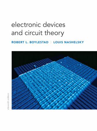
About the cover image: 17 : 17 cross-bar array of 50-nm thick TiO2 memristors defined by 50-nm wide platinum electrodes, spaced by 50-nm gaps. J. Joshua Yang, G. Medeiros-Ribeiro, and R. Stan Williams, Hewlett-Packard Labs. Copyright 2011, Hewlett-Packard Development Company, L. P. Reproduced with permission.
Cadence, The Cadence logo, OrCAD, OrCAD Capture, and PSpice are registered trademarks of Cadence Design Systems, Inc.
Multisim is a registered trademark of National Instruments.
Copyright © 2013, 2009, 2006 by Pearson Education, Inc. All rights reserved. Manufactured in the United States of America. This publication is protected by Copyright, and permission should be obtained from the publisher prior to any prohibited reproduction, storage in a retrieval system, or transmission in any form or by any means, electronic, mechanical, photocopying, recording, or likewise. To obtain permission(s) to use material from this work, please submit a written request to Pearson Education, Inc., Permissions Department, One Lake Street, Upper Saddle River, New Jersey 07458, or you may fax your request to 201-236-3290.
Many of the designations by manufacturers and sellers to distinguish their products are claimed as trademarks. Where those designations appear in this book, and the publisher was aware of a trademark claim, the designations have been printed in initial caps or all caps.
Library of Congress Cataloging-in-Publication Data
Boylestad, Robert L. Electronic devices and circuit theory / Robert L. Boylestad, Louis Nashelsky.—11th ed. p. cm. ISBN 978-0-13-262226-4 1. Electronic circuits. 2. Electronic apparatus and appliances. I. Nashelsky, Louis. II. Title. TK7867.B66 2013 621.3815—dc23
2011052885
10 9 8 7 6 5 4 3 2 1
ISBN 10: 0-13-262226-2 ISBN 13: 978-0-13-262226-4

DEDICATION
To Else Marie, Alison and Mark, Eric and Rachel, Stacey and Jonathan, and our eight granddaughters: Kelcy, Morgan, Codie, Samantha, Lindsey,
Britt, Skylar, and Aspen.
To Katrin, Kira and Thomas, Larren and Patricia, and our six grandsons: Justin, Brendan, Owen, Tyler, Colin, and Dillon.

This page intentionally left blank

The preparation of the preface for the 11th edition resulted in a bit of reflection on the 40 years since the first edition was published in 1972 by two young educators eager to test their ability to improve on the available literature on electronic devices. Although one may prefer the term semiconductor devices rather than electronic devices, the first edition was almost exclusively a survey of vacuum-tube devices—a subject without a single section in the new Table of Contents. The change from tubes to predominantly semiconductor devices took almost five editions, but today it is simply referenced in some sections. It is interest-ing, however, that when field-effect transistor (FET) devices surfaced in earnest, a number of the analysis techniques used for tubes could be applied because of the similarities in the ac equivalent models of each device.
We are often asked about the revision process and how the content of a new edition is defined. In some cases, it is quite obvious that the computer software has been updated, and the changes in application of the packages must be spelled out in detail. This text was the first to emphasize the use of computer software packages and provided a level of detail unavailable in other texts. With each new version of a software package, we have found that the supporting literature may still be in production, or the manuals lack the detail for new users of these packages. Sufficient detail in this text ensures that a student can apply each of the software packages covered without additional instruc-tional material.
The next requirement with any new edition is the need to update the content reflecting changes in the available devices and in the characteristics of commercial devices. This can require extensive research in each area, followed by decisions regarding depth of coverage and whether the listed improvements in response are valid and deserve recog-nition. The classroom experience is probably one of the most important resources for defining areas that need expansion, deletion, or revision. The feedback from students results in marked-up copies of our texts with inserts creating a mushrooming copy of the material. Next, there is the input from our peers, faculty at other institutions using the text, and, of course, reviewers chosen by Pearson Education to review the text. One source of change that is less obvious is a simple rereading of the material following the passing of the years since the last edition. Rereading often reveals material that can be improved, deleted, or expanded.
For this revision, the number of changes far outweighs our original expectations. How-ever, for someone who has used previous editions of the text, the changes will probably be less obvious. However, major sections have been moved and expanded, some 100-plus problems have been added, new devices have been introduced, the number of applications has been increased, and new material on recent developments has been added through-out the text. We believe that the current edition is a significant improvement over the previous editions.
As instructors, we are all well aware of the importance of a high level of accuracy required for a text of this kind. There is nothing more frustrating for a student than to work a problem over from many different angles and still find that the answer differs from the solution at the back of the text or that the problem seems undoable. We were pleased to find that there were fewer than half a dozen errors or misprints reported since
v
PREFACE

vi PREFACE the last edition. When you consider the number of examples and problems in the text along with the length of the text material, this statistic clearly suggests that the text is as error-free as possible. Any contributions from users to this list were quickly acknowl-edged, and the sources were thanked for taking the time to send the changes to the pub-lisher and to us.
Although the current edition now reflects all the changes we feel it should have, we expect that a revised edition will be required somewhere down the line. We invite you to respond to this edition so that we can start developing a package of ideas and thoughts that will help us improve the content for the next edition. We promise a quick response to your comments, whether positive or negative.
NEW TO THIS EDITION • Throughout the chapters, there are extensive changes in the problem sections. Over 100
new problems have been added, and a significant number of changes have been made to the existing problems.
• A significant number of computer programs were all rerun and the descriptions updated to include the effects of using OrCAD version 16.3 and Multisim version 11.1. In addi-tion, the introductory chapters are now assuming a broader understanding of computer methods, resulting in a revised introduction to the two programs.
• Throughout the text, photos and biographies of important contributors have been added. Included among these are Sidney Darlington, Walter Schottky, Harry Nyquist, Edwin Colpitts, and Ralph Hartley.
• New sections were added throughout the text. There is now a discussion on the impact of combined dc and ac sources on diode networks, of multiple BJT networks, VMOS and UMOS power FETs, Early voltage, frequency impact on the basic elements, effect of RS on an amplifier’s frequency response, gain-bandwidth product, and a number of other topics.
• A number of sections were completely rewritten due to reviewers’ comments or changing priorities. Some of the areas revised include bias stabilization, current sources, feedback in the dc and ac modes, mobility factors in diode and transistor response, transition and diffusion capacitive effects in diodes and transistor response characteristics, reverse-saturation current, breakdown regions (cause and effect), and the hybrid model.
• In addition to the revision of numerous sections described above, there are a number of sections that have been expanded to respond to changes in priorities for a text of this kind. The section on solar cells now includes a detailed examination of the materials employed, additional response curves, and a number of new practical applications. The coverage of the Darlington effect was totally rewritten and expanded to include detailed examination of the emitter-follower and collector gain configurations. The coverage of transistors now includes details on the cross-bar latch transistor and carbon nanotubes. The discussion of LEDs includes an expanded discussion of the materials employed, comparisons to today’s other lighting options, and examples of the products defining the future of this important semiconductor device. The data sheets commonly included in a text of this type are now discussed in detail to ensure a well-established link when the student enters the industrial community.
• Updated material appears throughout the text in the form of photos, artwork, data sheets, and so forth, to ensure that the devices included reflect the components avail-able today with the characteristics that have changed so rapidly in recent years. In addition, the parameters associated with the content and all the example problems are more in line with the device characteristics available today. Some devices, no longer available or used very infrequently, were dropped to ensure proper emphasis on the current trends.
• There are a number of important organizational changes throughout the text to ensure the best sequence of coverage in the learning process. This is readily apparent in the early dc chapters on diodes and transistors, in the discussion of current gain in the ac chapters for BJTs and JFETs, in the Darlington section, and in the frequency response chapters. It is particularly obvious in Chapter 16 , where topics were dropped and the order of sections changed dramatically.

viiPREFACE INSTRUCTOR SUPPLEMENTS To download the supplements listed below, please visit: http://www.pearsonhighered.com/irc and enter “Electronic Devices and Circuit Theory” in the search bar. From there, you will be able to register to receive an instructor’s access code. Within 48 hours after registering, you will receive a confirming email, including an instructor access code. Once you have received your code, return to the site and log on for full instructions on how to download the materials you wish to use.
PowerPoint Presentation –(ISBN 0132783746). This supplement contains all figures from the text as well as a new set of lecture notes highlighting important concepts.
TestGen® Computerized Test Bank –(ISBN 013278372X). This electronic bank of test questions can be used to develop customized quizzes, tests, and/or exams.
Instructor’s Resource Manual –(ISBN 0132783738). This supplement contains the solu-tions to the problems in the text and lab manual.
STUDENT SUPPLEMENTS Laboratory Manual –(ISBN 0132622459) . This supplement contains over 35 class-tested experiments for students to use to demonstrate their comprehension of course material.
Companion Website –Student study resources are available at www.pearsonhighered.com/boylestad
ACKNOWLEDGMENTS The following individuals supplied new photographs for this edition.
Sian Cummings International Rectifier Inc. Michele Drake Agilent Technologies Inc. Edward Eckert Alcatel-Lucent Inc. Amy Flores Agilent Technologies Inc. Ron Forbes B&K Precision Corporation Christopher Frank Siemens AG Amber Hall Hewlett-Packard Company Jonelle Hester National Semiconductor Inc. George Kapczak AT&T Inc. Patti Olson Fairchild Semiconductor Inc. Jordon Papanier LEDtronics Inc. Andrew W. Post Vishay Inc. Gilberto Ribeiro Hewlett-Packard Company Paul Ross Alcatel-Lucent Inc. Craig R. Schmidt Agilent Technologies, Inc. Mitch Segal Hewlett-Packard Company Jim Simon Agilent Technologies, Inc. Debbie Van Velkinburgh Tektronix, Inc. Steve West On Semiconductor Inc. Marcella Wilhite Agilent Technologies, Inc. Stan Williams Hewlett-Packard Company J. Joshua Wang Hewlett-Packard Company