
ELECTRONIC DEVICES LABORATORY Prepared by - Sri ...
79
SRI CHANDRASEKHARENDRA SARASWATHI VISWA MAHAVIDYALAYA (University established under section 3of UGC Act 1956) (Accredited with ‘A’ Grade by NAAC) Enathur, Kanchipuram – 631 561 DEPARTMENT OF ELECTRONICS AND COMMUNICATION ENGINEERING LABORATORY MANUAL FOR ELECTRONIC DEVICES LABORATORY FULL TIME B.E., II YEAR / III SEMESTER Prepared by : Dr.S.Omkumar, ECE Shri. R.Palani, Lab. Instructor/ECE Approved by : Prof.V.Swaminathan, HOD/ECE
-
Upload
khangminh22 -
Category
Documents
-
view
0 -
download
0
Transcript of ELECTRONIC DEVICES LABORATORY Prepared by - Sri ...

SRI CHANDRASEKHARENDRA SARASWATHI VISWA MAHAVIDYALAYA (University established under section 3of UGC Act 1956)
(Accredited with ‘A’ Grade by NAAC)
Enathur, Kanchipuram – 631 561
DEPARTMENT OF ELECTRONICS AND COMMUNICATION ENGINEERING
LABORATORY MANUAL FOR
ELECTRONIC DEVICES LABORATORY FULL TIME B.E., II YEAR / III SEMESTER
Prepared by : Dr.S.Omkumar, ECE
Shri. R.Palani, Lab. Instructor/ECE
Approved by : Prof.V.Swaminathan, HOD/ECE

DEPARTMENT OF ELECTRONICS AND
COMMUNICATION ENGINEERING
SRI CHANDRASEKHARENDRA SARASWATHI VISWA
MAHAVIDYALAYA
ELECTRONIC DEVICES
LABORATORY MANUAL
REGISTER NUMBER :
NAME OF THE STUDENT :
YEAR / SEM :

INDEX
Ex.no
Date
Name Of The Experiment Page
No:
Sign
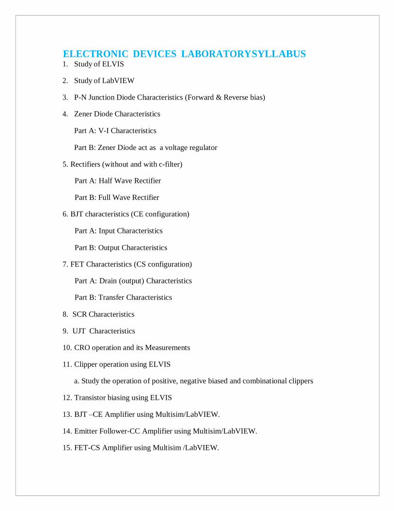
ELECTRONIC DEVICES LABORATORY SYLLABUS 1. Study of ELVIS
2. Study of LabVIEW
3. P-N Junction Diode Characteristics (Forward & Reverse bias)
4. Zener Diode Characteristics
Part A: V-I Characteristics
Part B: Zener Diode act as a voltage regulator
5. Rectifiers (without and with c-filter)
Part A: Half Wave Rectifier
Part B: Full Wave Rectifier
6. BJT characteristics (CE configuration)
Part A: Input Characteristics
Part B: Output Characteristics
7. FET Characteristics (CS configuration)
Part A: Drain (output) Characteristics
Part B: Transfer Characteristics
8. SCR Characteristics
9. UJT Characteristics
10. CRO operation and its Measurements
11. Clipper operation using ELVIS
a. Study the operation of positive, negative biased and combinational clippers
12. Transistor biasing using ELVIS
13. BJT –CE Amplifier using Multisim/LabVIEW.
14. Emitter Follower-CC Amplifier using Multisim/LabVIEW.
15. FET-CS Amplifier using Multisim /LabVIEW.
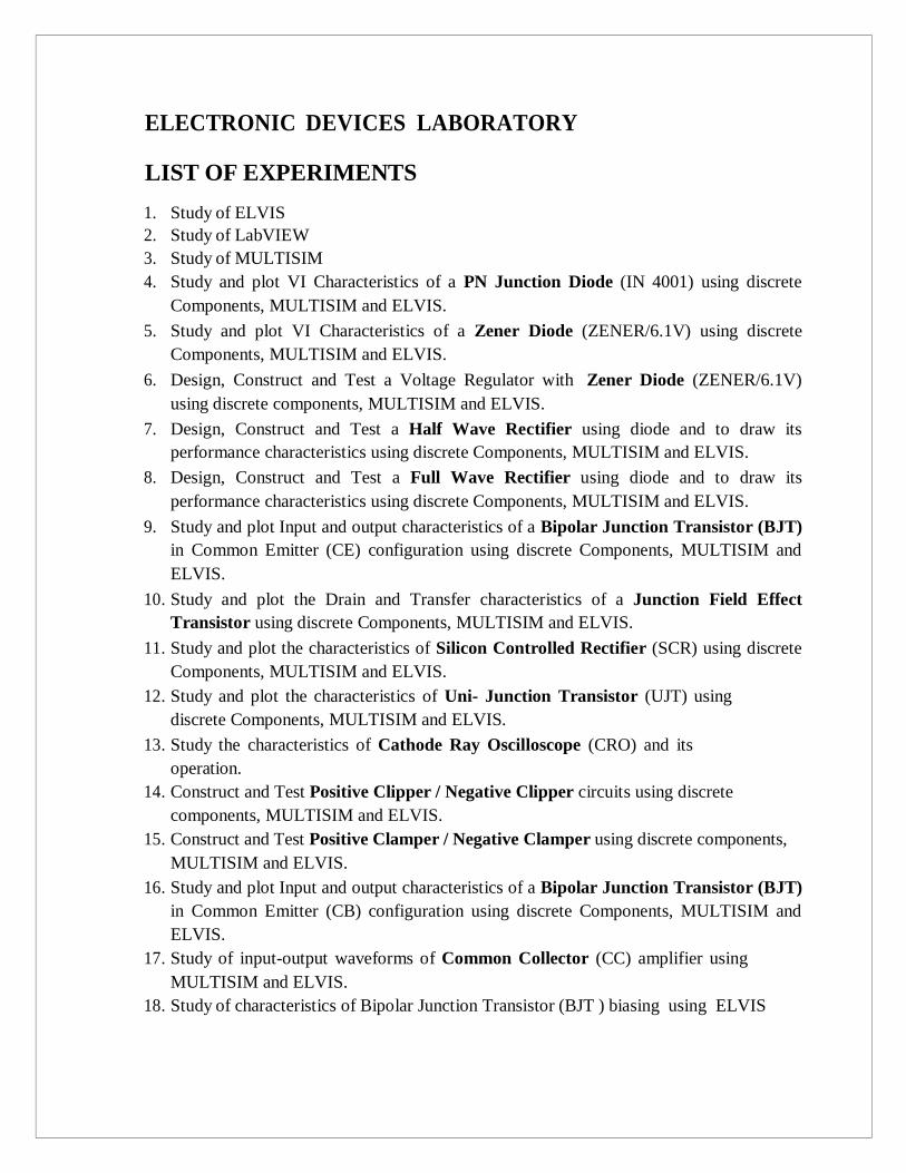
ELECTRONIC DEVICES LABORATORY
LIST OF EXPERIMENTS
1. Study of ELVIS
2. Study of LabVIEW
3. Study of MULTISIM
4. Study and plot VI Characteristics of a PN Junction Diode (IN 4001) using discrete
Components, MULTISIM and ELVIS.
5. Study and plot VI Characteristics of a Zener Diode (ZENER/6.1V) using discrete
Components, MULTISIM and ELVIS.
6. Design, Construct and Test a Voltage Regulator with Zener Diode (ZENER/6.1V)
using discrete components, MULTISIM and ELVIS.
7. Design, Construct and Test a Half Wave Rectifier using diode and to draw its
performance characteristics using discrete Components, MULTISIM and ELVIS.
8. Design, Construct and Test a Full Wave Rectifier using diode and to draw its
performance characteristics using discrete Components, MULTISIM and ELVIS.
9. Study and plot Input and output characteristics of a Bipolar Junction Transistor (BJT)
in Common Emitter (CE) configuration using discrete Components, MULTISIM and
ELVIS.
10. Study and plot the Drain and Transfer characteristics of a Junction Field Effect
Transistor using discrete Components, MULTISIM and ELVIS.
11. Study and plot the characteristics of Silicon Controlled Rectifier (SCR) using discrete
Components, MULTISIM and ELVIS.
12. Study and plot the characteristics of Uni- Junction Transistor (UJT) using
discrete Components, MULTISIM and ELVIS.
13. Study the characteristics of Cathode Ray Oscilloscope (CRO) and its
operation.
14. Construct and Test Positive Clipper / Negative Clipper circuits using discrete
components, MULTISIM and ELVIS.
15. Construct and Test Positive Clamper / Negative Clamper using discrete components,
MULTISIM and ELVIS.
16. Study and plot Input and output characteristics of a Bipolar Junction Transistor (BJT)
in Common Emitter (CB) configuration using discrete Components, MULTISIM and
ELVIS.
17. Study of input-output waveforms of Common Collector (CC) amplifier using
MULTISIM and ELVIS.
18. Study of characteristics of Bipolar Junction Transistor (BJT ) biasing using ELVIS

Introduction
There are 3 hours allocated to a Electronic Devices and Circuits Laboratory
session in lab. It is a necessary part of the course at which attendance is
compulsory.
Here are some guidelines to help you perform the experiments and to submit the
Reports:
1. Read all instructions carefully and carry them all out.
2. Ask the demonstrator if you are unsure of anything.
3. Record actual results (comment on them if they are unexpected!)
4. Write up full and suitable conclusions for each experiment.
5. If you have any doubt about the safety of any procedure, contact
the demonstrator beforehand.
6. THINK about what you are doing!

Course Designed
by
Department of Electronics and Communication Engineering
Category Simulation based Experiments
(SBE)
Discrete based Experiments
(DBE)
Broad Area of
Syllabus
ELECTRONICS DEVICES LABORATORY
Staffs Responsible
for Preparation
of Contents in the
Manual
Dr.S.Omkumar, Asso.Prof/ECE
Shri.R.PALANI, Lab Instructor/ECE
Date of
Preparation
June 2021 Approved by: Prof. V.Swaminathan
HOD/ ECE

1 | P a g e
STUDY OF ELVIS
EX.NO: 1 DATE:
AIM:
To Study the NI ELVIS.
THEORY:
Educational Laboratory Virtual Instrumentation Suite (ELVIS) Virtual instrumentation is defined as the
combination of measurement and control hardware and application software with industry-standard
computer technology to create user-defined instrumentation systems
Virtual instrumentation provides an ideal platform for developing instructional curriculum and
conducting scientific research. The modular nature of virtual instrumentation makes it easy to add new
functionality. NI ELVIS uses LabVIEW-based software and NI data acquisition hardware to create a
virtual instrumentation system that provides the functionality of a suite of instruments.
1. Concepts in Context
Projects that inherently challenge to employ innovative design thinking often involve interacting with an
unknown process or device. Designing a test in this style not only requires an understanding of
specifications, the limitations of the equipment, and the fundamental concepts being applied but it also
requires to contend with outside factors and how one change can have a cascading effect on the
experimental setup.
Figure 1: Topic distribution of the Fundamentals series of courses
Fundamentals seeks to convey the fundamentals of electrical engineering including circuits, electronics,
and signals and systems all in one series of courses that iteratively build on each other. So rather than
teaching Operational Amplifiers as an individual topic, the signals that go into the OpAmp and how
those characteristics influence the performance of the OpAmp is analysed. OpAmps, and signals to fully
comprehend every element of the project.

2 | P a g e
Figure 2: Fundamentals I at UVA final summing amplifier project
To most effectively analyze concepts in this manner, the ability to effectively instrument and analyze the
experiment, but precise control and the ability to manipulate the type and behavior of the inputs to the
system are critical for understanding. The NI ELVIS II is the only engineering laboratory solution that
combines 7 traditional instruments with fully customizable I/O, enabling complete implementation of the
concepts in context approach.
Figure 3: NI ELVIS II instrumentation specifications

3 | P a g e
The NI ELVIS II combines instrumentation and control specifically to service experiments and learning
experiences like this one. The need to create a controller which precisely shakes a beam yet the
amplifier for the shaker and the signal conditioning for the force transducer needs to be stable and
accurate to ensure a successful experiment. Instruments such as a 4-channel oscilloscope and a 16-
channel logic analyzer givesthe security of knowing the results of their experiment are valid.
Figure 4: NI ELVIS II control I/O specifications
Figure 5: Output waveform of EKG in LabVIEW

4 | P a g e
NI ELVIS II enables to teach innovation by allowing to challenge with more projects that follow the
engineering design process.
(a) an ability to apply knowledge of mathematics, science and engineering
(d) an ability to function on multidisciplinary teams
(e) an ability to identify, formulate, and solve engineering problems
(k) an ability to use the techniques, skills, and modern engineering tools necessary for engineering
practice
RESULT:
Thus the Study of NI ELVIS was done successfully.
5 | P a g e
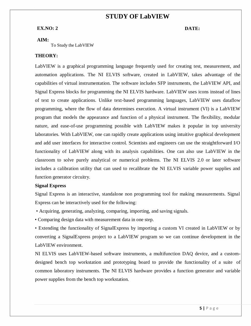
STUDY OF LabVIEW
EX.NO: 2 DATE:
AIM: To Study the LabVIEW
THEORY:
LabVIEW is a graphical programming language frequently used for creating test, measurement, and
automation applications. The NI ELVIS software, created in LabVIEW, takes advantage of the
capabilities of virtual instrumentation. The software includes SFP instruments, the LabVIEW API, and
Signal Express blocks for programming the NI ELVIS hardware. LabVIEW uses icons instead of lines
of text to create applications. Unlike text-based programming languages, LabVIEW uses dataflow
programming, where the flow of data determines execution. A virtual instrument (VI) is a LabVIEW
program that models the appearance and function of a physical instrument. The flexibility, modular
nature, and ease-of-use programming possible with LabVIEW makes it popular in top university
laboratories. With LabVIEW, one can rapidly create applications using intuitive graphical development
and add user interfaces for interactive control. Scientists and engineers can use the straightforward I/O
functionality of LabVIEW along with its analysis capabilities. One can also use LabVIEW in the
classroom to solve purely analytical or numerical problems. The NI ELVIS 2.0 or later software
includes a calibration utility that can used to recalibrate the NI ELVIS variable power supplies and
function generator circuitry.
Signal Express
Signal Express is an interactive, standalone non programming tool for making measurements. Signal
Express can be interactively used for the following:
• Acquiring, generating, analyzing, comparing, importing, and saving signals.
• Comparing design data with measurement data in one step.
• Extending the functionality of SignalExpress by importing a custom VI created in LabVIEW or by
converting a SignalExpress project to a LabVIEW program so we can continue development in the
LabVIEW environment.
NI ELVIS uses LabVIEW-based software instruments, a multifunction DAQ device, and a custom-
designed bench top workstation and prototyping board to provide the functionality of a suite of
common laboratory instruments. The NI ELVIS hardware provides a function generator and variable
power supplies from the bench top workstation.

6 | P a g e
Using NI ELVIS in Signal Express
To use an NI ELVIS instrument within Signal Express complete the following steps: 1. Launch Signal
Express.
1. Click the Add Step button.
2. If NI ELVIS 2.0 or later is installed, NI ELVIS is in the list of steps. Expand NI ELVIS. 3. Choose
the instrument to add under Analog or Digital»Acquire or Generate Signals.
4. Click the Configure button to select the DAQ device cabled to the NI ELVIS Benchtop
Workstation.
5. Set the various controls on the configuration panel appropriately for the measurement.
6. Run the Signal Express project.
NI ELVIS LabVIEW
The NI ELVIS LabVIEW soft front panel (SFP) instruments combined with the functionality of the
DAQ device and the NI ELVIS workstation provide the functionality of the following SFP instruments:
• Arbitrary Waveform Generator (ARB)
• Bode Analyzer Digital Bus Reader
• Digital Bus Writer
• Digital Multimeter (DMM)
• Dynamic Signal Analyzer (DSA)
• Function Generator (FGEN)
• Impedance Analyzer
• Oscilloscope (Scope)
• Two-Wire Current Voltage Analyzer
• Three-Wire Current Voltage Analyzer
• Variable Power Supplies
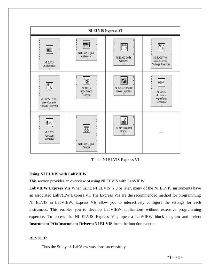
7 | P a g e
Table: NI ELVIS Express VI
Using NI ELVIS with LabVIEW
This section provides an overview of using NI ELVIS with LabVIEW.
LabVIEW Express VIs When using NI ELVIS 2.0 or later, many of the NI ELVIS instruments have
an associated LabVIEW Express VI. The Express VIs are the recommended method for programming
NI ELVIS in LabVIEW. Express VIs allow you to interactively configure the settings for each
instrument. This enables you to develop LabVIEW applications without extensive programming
expertise. To access the NI ELVIS Express VIs, open a LabVIEW block diagram and select
Instrument I/O»Instrument Drivers»NI ELVIS from the function palette.
RESULT:
Thus the Study of LabView was done successfully.

8 | P a g e
STUDY OF MULTISIM
EX.NO: 3 DATE:
AIM:
To Study the operational Amplifier using MULTISIM Software
THEORY:
The purpose of this study is to demonstrate the use of MultiSim to simulate operational amplifier
circuits (μA741 OpAmp), such as inverting and non-inverting amplifiers, filters, and oscillators. The
circuit shown in Figure 1 is used as a simulation example in the current tutorial.
Figure 1. An inverting unity gain operational amplifier circuit
1) Start the MultiSim program as shown in the previous tutorial (For Windows users the default
location can be found by clicking: Start ->All Programs -> Electronics Workbench ->
DesignSuite Freeware Edition 9 -> MultiSim 9).
2) We will be creating a new schematic and simulation so choose File->SaveAs, navigate to
or create a directory where we can save this schematic and simulation then fill in the filename as
shown below. (I called this one tut1.) Click OK when we have navigated to the proper directory and
entered a name for the project.
3) We should now have a blank schematic. Start placing components by selecting Place-
>Component from the menu bar. We will see another dialog box as shown. Start with the OpAmp
so pick Analog Components in the drop down menu as shown:
9 | P a g e
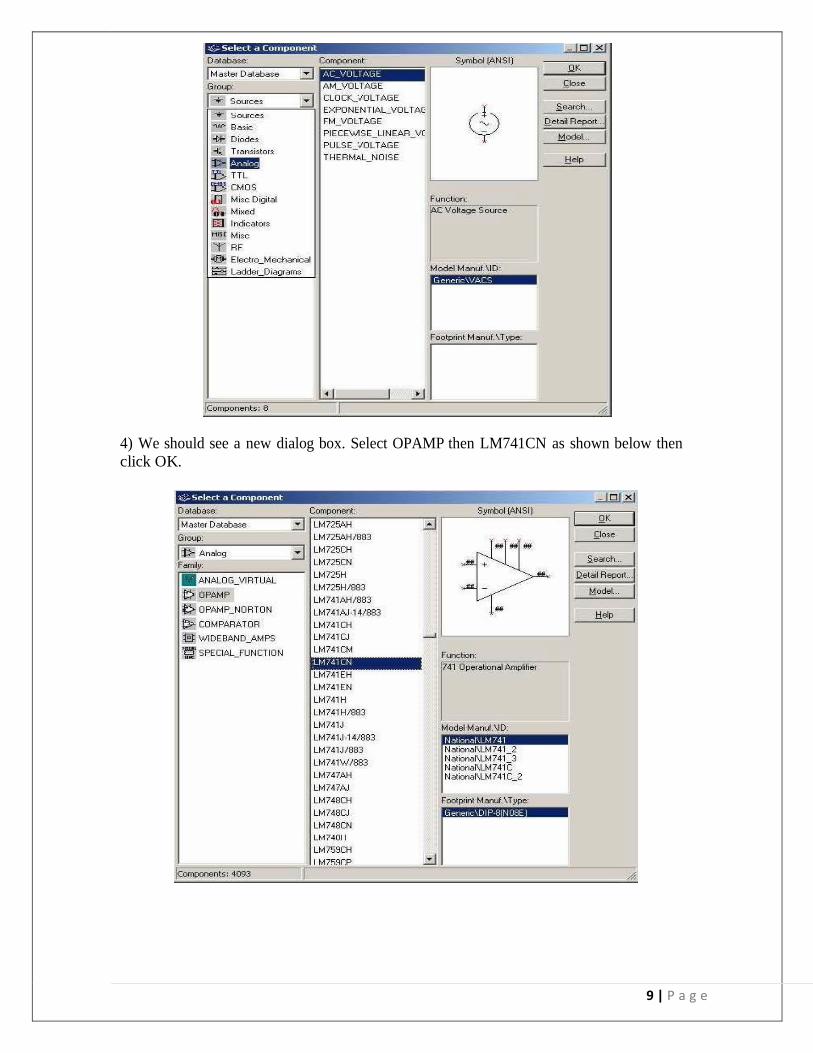
4) We should see a new dialog box. Select OPAMP then LM741CN as shown below then
click OK.
10 | P a g e
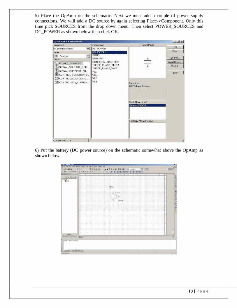
5) Place the OpAmp on the schematic. Next we must add a couple of power supply
connections. We will add a DC source by again selecting Place->Component. Only this
time pick SOURCES from the drop down menu. Then select POWER_SOURCES and
DC_POWER as shown below then click OK.
6) Put the battery (DC power source) on the schematic somewhat above the OpAmp as
shown below.

11 | P a g e
7) Double click on the “12V”. Change the voltage from 12 to 18 then click OK.
8) Place the rest of the components on the schematic as shown below. Use Place->Wire
to add wires for connecting components together. Resistors are under the Basic
components drop down menu. Note we must specify “k_” in the filter to locate the 10K
resistors. Note GROUND symbols are at SOURCES->POWER_SOURCES. Wer
completed schematic should resemble the one below.
9) Be sure all components are connected as shown above. Now we will name the input
and output signals to make them easier to locate in simulation. First highlight the wires
above the 5V 1KHz source V3. Do this by placing the cursor on the red wire and left
clicking once. Now right click once and select “properties” from the popup menu. Change the net name to Vin as shown on the next page then click OK. Use the same
method to change the output net name to “Vout”.

12 | P a g e
10) We will now run a simulation. First select Simulate->Analyses->Transient Analysis
from the top menu bar. Change the End Stop Time (TSTOP) to 0.002 as shown below.
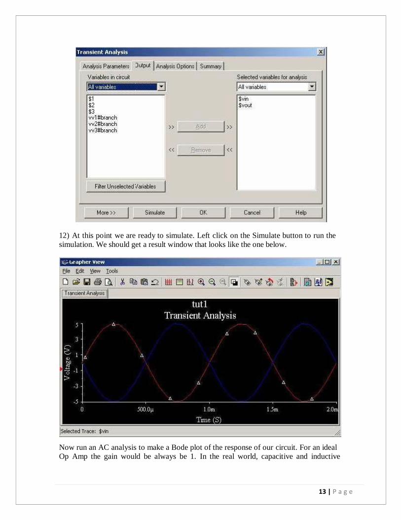
11) Next choose the Output page and select the two signals we want to see on the output.
Wer dialog box should now look like the one on the next page.
13 | P a g e
12) At this point we are ready to simulate. Left click on the Simulate button to run the
simulation. We should get a result window that looks like the one below.
Now run an AC analysis to make a Bode plot of the response of our circuit. For an ideal
Op Amp the gain would be always be 1. In the real world, capacitive and inductive
14 | P a g e
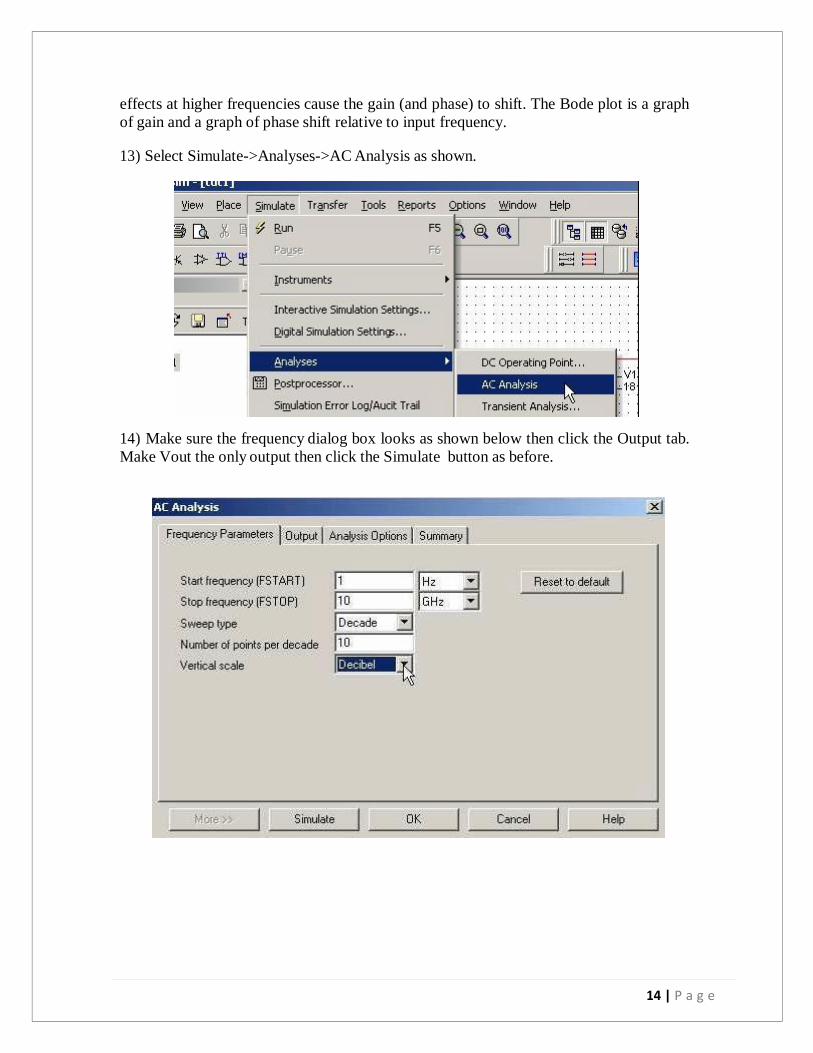
effects at higher frequencies cause the gain (and phase) to shift. The Bode plot is a graph
of gain and a graph of phase shift relative to input frequency.
13) Select Simulate->Analyses->AC Analysis as shown.
14) Make sure the frequency dialog box looks as shown below then click the Output tab.
Make Vout the only output then click the Simulate button as before.

15 | P a g e
15) The simulation results should appear as below. Note the top graph is gain in decibels
(0 db is the same as unity gain or 1). See how the gain rolls off starting around 1 MHz.
The bottom graph is phase shift. Since this is an inverting configuration, expect the phase
shift to be 180 degrees. But notice how it drops to around 90 degrees by 10MHz then
rolls down to around 0 by 10GHz.
16) Put the cursor in the graph and right click to get the menu show. From there we can
turn the grids on or off, add cursors, etc. we can also choose Properties and change the
axes of the graphs. Use File->Print to print the Bode plot.
RESULT:
Thus the study of operational Amplifier using MULTISIM was done successfully.

16 | P a g e
17 | P a g e
1k +A
+
RPS 30 V
FORWARD BIAS CHARACTERISTICS:
.
(0-25) mA
(0-3)V
MODEL GRAPH:
REVERSE BIAS CHARACTERISTICS:
1N
400
7
18 | P a g e
CHARACTERISTICS OF PN DIODE
EX.NO: 4 DATE:
AIM:
To Study and plot VI Characteristics of a PN Junction Diode (IN 4001) using discrete
Components, MULTISIM and ELVIS. Also calculate the forward resistance ‘RF’ and cut- in voltage.
COMPONENTS & EQUIPMENTS REQUIRED:
S.No APPARATUS RANGE QUANTITY
1 PN Junction diode IN 4001 1
2 Resistor 1 K 1
3 Ammeter (0-30) mA, (0-500) A Each 1
4 Voltmeter (0-30)V, (0-3)V Each 1
5 Regulated Power Supply (0-30)V 1
6 Bread board - 1
7 Connecting wires - Few
THEORY:
When a P and N type semi-conductors are formed together a P-N junction is created.
There are two types of biasing. When a P-type semiconductor is connected to positive
terminal of the battery and N-type Semiconductor to the negative terminal, the junction
barrier vanishes leading to forward current. But when connections are interchanged the
junction barrier increases very much leading to no current flow. But a small value of current,
due to the minority carriers, known as reverse saturation current, is present there.
PROCEDURE:
1. Connections are given as per the circuit diagram.
2. Input supply voltage is varied.
3. The corresponding forward voltage and current are noted.
4. The readings are tabulated and the graph is plotted between the voltage on X-axis
and current on Y-axis.
5. From the graph, the forward resistance RF =Vf/If and the cut-in voltage are
calculated.

19 | P a g e
Sl.
No.
VIN
(in Volts)
Vf
(in Volts)
If
(in mA)
Sl.
No.
VIN
(in Volts)
VR
(in Volts)
IR
(in μA)
TABULATION:
Forward Bias Reverse Bias
CALCULATIONS:

20 | P a g e
RESULT:
Thus the forward and reverse characteristics of a PN junction diode were plotted and the
following observations were made.
Forward resistance =
Cut-in voltage =

21 | P a g e
R 1k +
A
+
RPS 30 V
FORWARD BIAS CHARACTERISTICS:
(0-25) mA
(0-3)V
MODEL GRAPH:
REVERSE BIAS CHARACTERISTICS:
BZ
D2
7-C
6V
8
22 | P a g e
CHARACTERISTICS OF ZENER DIODE
EX.NO:5 DATE:
AIM:
To Study and plot VI Characteristics of a Zener Diode using discrete
Components, MULTISIM and ELVIS. Also to find the value of forward resistance, cut-
in voltage and breakdown voltage.
COMPONENTS & EQUIPMENTS REQUIRED:
S.No APPARATUS RANGE QUANTITY
1. Zener diode 6.1V Zener Diode 1
2. Resistor 1 K 1
3. Ammeter (0-30) mA 1
4. Voltmeter (0-30)V,(0-3)V Each1
5 Regulated Power Supply (0-30)V 1
6 Bread board - 1
7 Connecting wires - Few
THEORY:
A Zener Diode conducts both in forward and reverse biased condition. In the forward
bias condition, it acts like an ordinary PN-junction diode. But in reverse bias, due to
avalanche breakdown at a particular value of voltage, known as Zener voltage, the current
starts increasing abruptly even if the reverse voltage is kept constant. Hence Zener Diode is
used as voltage regulator.
PROCEDURE:
1. Connections are given as per the circuit diagram.
2. Input supply voltage is varied.
3. The corresponding forward voltage and current are noted.
4. The readings are tabulated and the graph is plotted between the voltage on x-axis and
current on y-axis.
5. From the graph the forward resistance RF = Vf/ If and cut-in voltage are calculated.

23 | P a g e
Sl.
No.
VIN
(in Volts)
Vf
(in Volts)
If
(in mA)
Sl.
No.
VIN
(in Volts)
VR
(in Volts)
IR
(in mA)
.
TABULATION:
Forward Bias Reverse Bias
CALCULATIONS:

24 | P a g e
RESULT:
Thus the forward and reverse characteristics of a Zener diode were plotted and following
observations were made.
Forward resistance =
Cut-in voltage =
Breakdown voltage =
25 | P a g e
CIRCUIT DIAGRAM:
MODEL GRAPH:
26 | P a g e
VOLTAGE REGULATOR USING ZENER DIODE
EX.NO: 6 DATE:
AIM:
To Design, Construct and Test a Voltage Regulator with Zener Diode using discrete
components, MULTISIM and ELVIS. Also to find its regulated voltage.
COMPONENTS & EQUIPMENTS REQUIRED:
S.No APPARATUS RANGE QUANTITY
1 Zener Diode Zener diode 1
2 Voltmeter (0-30) V 1
3 Resistor 100 1
4 Ammeter (0-50) mA 1
5 DRB Box - 1
6 Bread board - 1
7 Connecting wires - Few
THEORY:
The distinct property of the Zener diode as compared to ordinary P-N Jn diode is : it
maintains a constant voltage level when it is reverse biased. When the reverse voltage
exceeds the breakdown value, avalanche breakdown occurs. The electrons having acquired
higher momentum overcome the potential barrier. In this region, the diode has dynamic
resistance due to which current increases abruptly and its resistance decreases. Since the load
is connected in parallel, the voltage remains constant. Hence the name “constant voltage
regulator”.

27 | P a g e
Sl.NO Vin (V) VO (V) Il (mA)
Sl.NO Rl (Ω) VO (v) Il (mA)
TABULATION:
Line Regulation Load Regulation
RL = VIN =
CALCULATIONS:

28 | P a g e
PROCEDURE:
Line Regulation
1. The connection is made as per the circuit diagram
2. Keep the Load resistance value constant, say, RL= K .
3. Vary the input voltage and note down the corresponding output voltage.
4. Find the breakdown voltage value and also plot the graph.
Load Regulation
5. Keep the input voltage constant ,say, Vin =
6. Vary the Load resistance and note down the corresponding output voltage.
7. Find the breakdown voltage value and also plot the graph
RESULT:
A voltage regulator using Zener diode has been constructed and its
characteristics were verified.
Regulated voltage = ----------------------------------------

29 | P a g e
CIRCUIT DIAGRAM:
MODEL GRAPH:
30 | P a g e
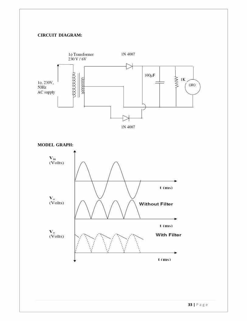
HALF WAVE RECTIFIER
EX.NO: 7 DATE:
AIM:
To construct a Half Wave Rectifier using diode and to draw its performance
characteristics using discrete Components, MULTISIM and ELVIS.
APPARATUS REQUIRED:
S.No APPARATUS RANGE QUANTITY
1 Transformer 230/(12-0-12)V 1 No
2 R.P.S (0-30)V 2
3
Ammeter (0–30)mA,
(0–250)μA
Each 1
4 Voltmeter (0–30)V, (0–2)V Each 1
5 Diode IN4001 1
6 Resistor 1KΩ 1
7 Capacitor 100μf 1
8 Bread Board - 1
9 Connecting wires - Few
THEORY:
In half wave rectifier only half cycle of applied AC voltage is used. Another half cycle of
AC voltage (negative cycle) is not used. Only one diode is used which conducts during
positive cycle. The circuit diagram of half wave rectifier without capacitor is shown in the
following figure. During positive half cycle of the input voltage anode of the diode is
positive compared with the cathode. Diode is in forward bias and current passes through the
diode and positive cycle develops across the load resistance RL. During negative half cycle
of input voltage, anode is negative with respected to cathode and diode is in reverse bias. No
current passes through the diode hence output voltage is zero.

31 | P a g e
TABULATION:
WITHOUT FILTER
Vm Vrms Vdc Ripple factor Efficiency
WITH FILTER
Vm Vrms Vdc Ripple factor Efficiency

32 | P a g e
PROCEDURE:
WITHOUT FILTER:
1. Give the connections as per the circuit diagram.
2. Give 230v, 50HZ I/P to the step down TFR where secondary connected to the
Rectifier I/P.
3. Take the rectifier output across the Load.
4. . Plot its performance graph.
WITH FILTER:
1. Give the connections as per the circuit diagram.
2. Give 230v, 50HZ I/P to the step down TFR where secondary connected to
the Rectifier I/P.
3. Connect the Capacitor across the Load.
4. Take the rectifier output across the Load.
5. Plot its performance graph.
FORMULAE:
WITHOUT FILTER:
(i) Vrms = Vm / Ö2
(ii) Vdc = Vm / Õ
(iii) Ripple Factor = Ö (Vrms / Vdc)2 – 1
(iv) Efficiency = (Vdc / Vrms)2 x 100
WITH FILTER:
(i) Vrms = Ö (Vrms’2 + Vdc2)
(ii) Vrms’ = Vrpp / (Ö3 x 2)
(iii) Vdc = Vm – V rpp / 2
(iv) Ripple Factor = Vrms’/ Vdc
RESULT:
Thus the performance characteristics of Half wave rectifier was obtained.
33 | P a g e
CIRCUIT DIAGRAM:
MODEL GRAPH:
34 | P a g e
FULL WAVE RECTIFIER
EX.NO: 8 DATE:
AIM:
To construct a Full Wave Rectifier using diode and to draw its performance characteristics
using discrete Components, MULTISIM and ELVIS.
COMPONENTS & EQUIPMENTS REQUIRED:
SNo APPARATUS RANGE QTY
1 Transformer 230 /(12-0-12)V 1
2 R.P.S (0-30)V 2
5 Diode IN4007 1
6 Resistor 1KΩ 1
7 Capacitor 100μf 1
8 Bread Board - 1
9 Connecting Wires - Few
THEORY:
The Bridge rectifier is a circuit, which converts an ac voltage to dc voltage using both half
cycles of the input ac voltage. The Bridge rectifier circuit is shown in the following figure. The
circuit has four diodes connected to form a bridge. The ac input voltage is applied to the
diagonally opposite ends of the bridge. The load resistance is connected between the other two
ends of the bridge. For the positive half cycle of the input ac voltage, diodes D1 and D2
conduct, whereas diodes D3 and D4 remain in the OFF state. The conducting diodes will be in
series with the load resistance RL and hence the load current flows through RL. For the
negative half cycle of the input ac voltage, diodes D3 and D4 conduct whereas, D1 and D2
remain OFF. The conducting diodes D3 and D4 will be in series with the load resistance RL and
hence the current flows through RL in the same direction as in the previous half cycle. Thus a bi-
directional wave is converted into a unidirectional wave

35 | P a g e
TABULATION:
Without Filter
Vm Vrms Vdc Ripple factor Efficiency
With Filter
Vrms Vrpp Vdc Ripple factor Efficiency
FORMULA:
Without Filter
(i) Vrms = Vm / √2
(ii) Vdc = 2Vm / ∏
(iii) RippleFactor = √(Vrms/Vdc)2
(iv) Efficiency = (Vdc/Vrms)2x100
With Filter
(i) Vrms = Vrpp/(2*√3)
(ii)
(iii)
Vdc
RippleFactor
Vm–V rpp
Vrms’/Vdc

36 | P a g e
PROCEDURE:
Without Filter
1. Give the connections as per the circuit diagram.
2. Give 230v, 50HZ I/P to the step down TFR where secondary connected to the
Rectifier I/P.
3. Take the rectifier output across the Load.
4. Plot its performance graph.
With Filter
5. Give the connections as per the circuit diagram.
6. Give 230v, 50HZ I/P to the step down TFR where secondary connected to the
Rectifier I/P.
7. Connect the Capacitor across the Load.
8. Take the rectifier output across the Load.
9. Plot its performance graph.
RESULT:
Thus the performance characteristics of Full wave rectifier were obtained.
37 | P a g e
CIRCUIT DIAGRAM:
MODEL GRAPH:
Input Characteristics of BJT
Output Characteristics of BJT

38 | P a g e
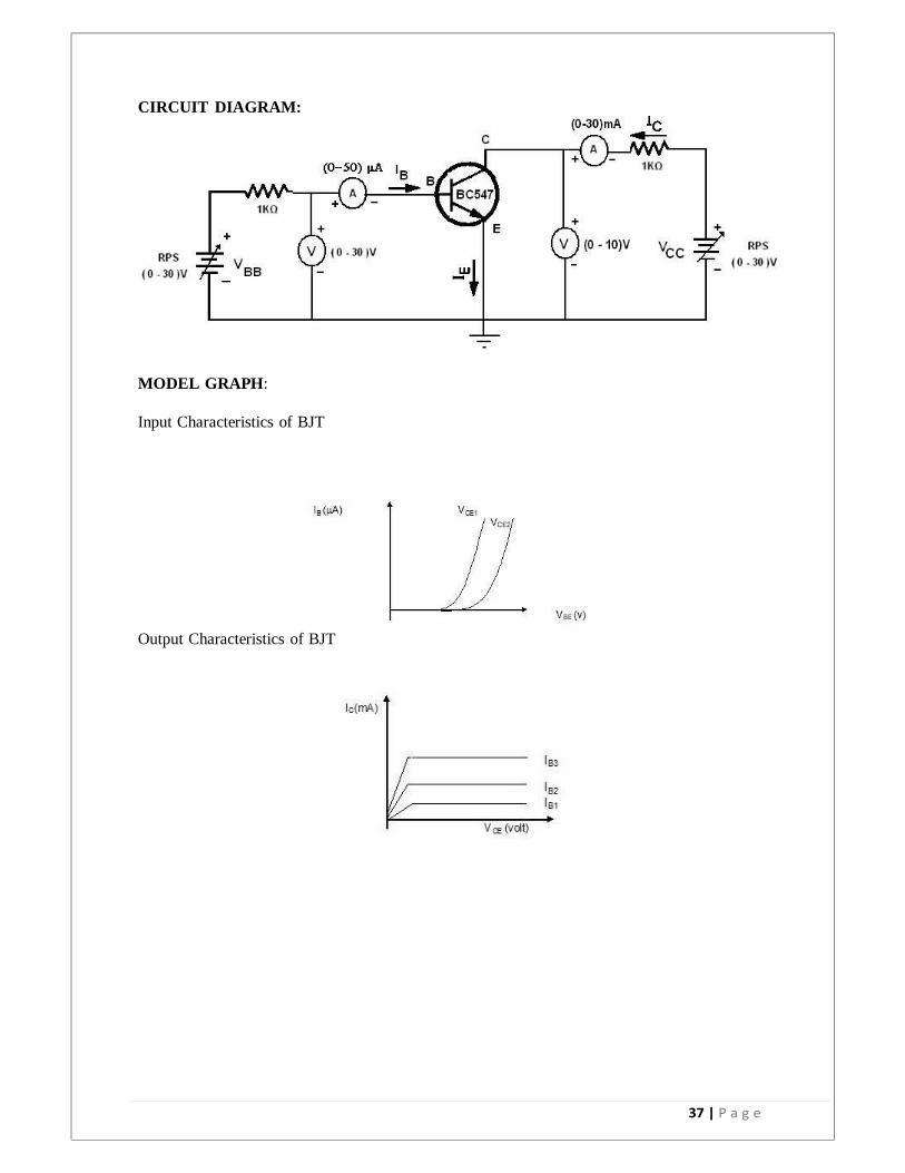
CHARACTERISTICS OF BJT IN CE CONFIGURATION
EX.NO: 9 DATE:
AIM:
To plot the input and output characteristics of a Bipolar Junction Transistor (BJT) in
Common Emitter (CE) configuration using discrete Components, MULTISIM and
ELVIS.
COMPONENTS & EQUIPMENTS REQUIRED:
S.NO APPARATUS RANGE QUANTITY
1 RPS (0-30)V 2
2 Resistor 1KΩ 2
3 DC Voltmeter (0-30)V 1
4 DC Voltmeter (0-10)V 1
5 DC Ammeter (0-500)µA 1
6 DC Ammeter (0-30)mA 1
7 BJT BC547/BC 107 1
8 Breadboard - 1
9 Connecting wires - Few
THEORY:
The input is applied between b a s e a n d e m i t t e r a n d o u t p u t is taken from
the collector and emitter. Here, emitter of the transistor is common to both input and
output circuits and hence the name common emitter (CE) configuration. Regardless
of circuit configuration, the base emitter junction is always forward biased while
the collector-base junction is always reverse biased, to operate transistor in active
region.

39 | P a g e
INPUT CHARACTERSTICS:
VCE =
S.NO VS (volt) VBE (volt) IB (μA)
OUTPUT CHARACTERSTICS:
IB =
S.NO VS (VOLTS) VCE(VOLTS) IC (mA)

40 | P a g e
PROCEDURE:
Input Characteristics
1) Connections are made as per the circuit diagram.
2) The output voltage VCE is kept constant.
3) By varying the input voltage VBE , the corresponding input currents IB are noted
down
4) A graph is plotted between VBE and IB.
5) The inverse slope of the curve gives forward input resistance.
Output Characteristics
1. Connections are made as per the circuit diagram.
2. The input current IB is kept constant.
3. By varying the output voltage VCE, the corresponding output current
IC is noted down.
4. A graph is plotted between VCE and IC .
5. The inverse slope of the curve gives forward output resistance.
RESULT:
The input and output characteristics of the transistor in CE mode are drawn and the
input and output resistances are calculated.
Input resistance =
Output resistance =

41 | P a g e
CIRCUIT DIAGRAM:
MODEL GRAPH:
Drain Characteristics
Transfer Characteristics
42 | P a g e
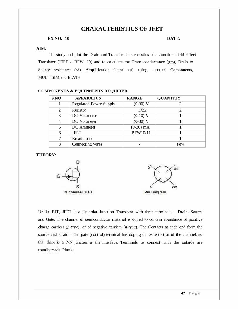
CHARACTERISTICS OF JFET
EX.NO: 10 DATE:
AIM:
To study and plot the Drain and Transfer characteristics of a Junction Field Effect
Transistor (JFET / BFW 10) and to calculate the Trans conductance (gm), Drain to
Source resistance (rd), Amplification factor (µ) using discrete Components,
MULTISIM and ELVIS
COMPONENTS & EQUIPMENTS REQUIRED:
S.NO APPARATUS RANGE QUANTITY
1 Regulated Power Supply (0-30) V 2
2 Resistor 1KΩ 2
3 DC Voltmeter (0-10) V 1
4 DC Voltmeter (0-30) V 1
5 DC Ammeter (0-30) mA 1
6 JFET BFW10/11 1
7 Bread board - 1
8 Connecting wires - Few
THEORY:
Unlike BJT, JFET is a Unipolar Junction Transistor with three terminals – Drain, Source
and Gate. The channel of semiconductor material is doped to contain abundance of positive
charge carriers (p-type), or of negative carriers (n-type). The Contacts at each end form the
source and drain. The gate (control) terminal has doping opposite to that of the channel, so
that there is a P-N junction at the interface. Terminals to connect with the outside are
usually made Ohmic.

43 | P a g e
TABULATION:
DRAIN CHARACTERISTICS
Sl.No. VS ( in Volts) VGS = VGS =
VDS (V) ID ( mA) VDS (V) ID ( mA)
CALCULATIONS:
Drain Resistance rd = VDS / Id
TRANSFER CHARACTERISTICS
Sl.No. VS ( in Volts) VDS =
VGS (V) ID ( mA)
CALCULATIONS:
Amplification factor (µ) = gm x rd
44 | P a g e
PROCEDURE:
The connections are given as per the circuit diagram.
DRAIN CHARACTERICTICS
1. Voltage VGS is kept at some fixed level.
2. The Drain to Source voltage VDS is varied and the corresponding drain current Id is
noted. The Graph was plotted between VDS on the x-axis and Id on y-axis.
3. The drain resistance (rd) was determined as rd = VDS / Id
TRANSFER CHARACTERICTICS
1. The VDS is kept at some particular value.
2. The Source voltage VGS is varied at some particular level and the corresponding
drain current Id was noted.
3. A graph was plotted between VGS and ID.
4. Transfer conductance value was determined by gm = Id / Vgs
RESULT:
Thus the Drain and transfer characteristics of the given JFET were studied and the
following values were determined.
a) Drain resistance (rd) =
b) Trans-Conductance (gm) =
c) Amplification factor (µ) =
45 | P a g e
CIRCUIT DIAGRAM:
MODEL GRAPH:
46 | P a g e
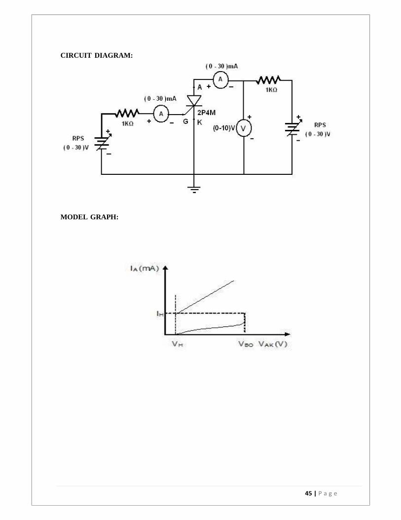
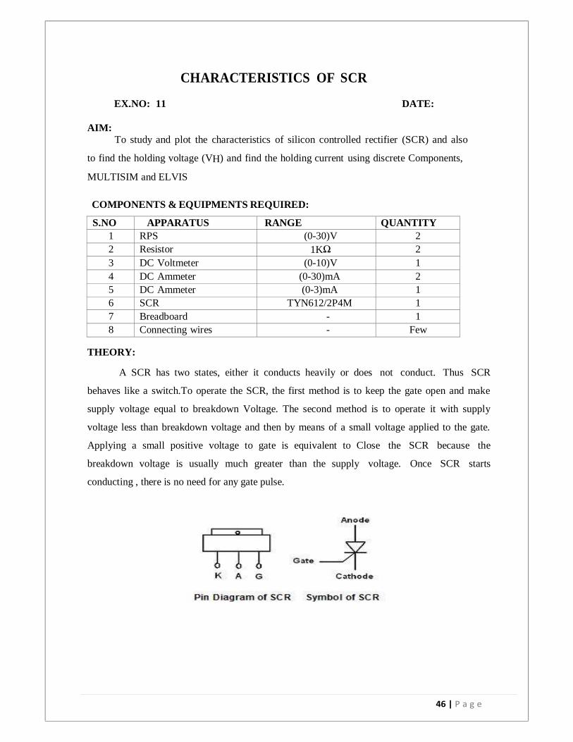
CHARACTERISTICS OF SCR
EX.NO: 11 DATE:
AIM:
To study and plot the characteristics of silicon controlled rectifier (SCR) and also
to find the holding voltage (VH) and find the holding current using discrete Components,
MULTISIM and ELVIS
COMPONENTS & EQUIPMENTS REQUIRED:
S.NO APPARATUS RANGE QUANTITY
1 RPS (0-30)V 2
2 Resistor 1KΩ 2
3 DC Voltmeter (0-10)V 1
4 DC Ammeter (0-30)mA 2
5 DC Ammeter (0-3)mA 1
6 SCR TYN612/2P4M 1
7 Breadboard - 1
8 Connecting wires - Few
THEORY:
A SCR has two states, either it conducts heavily or does not conduct. Thus SCR
behaves like a switch.To operate the SCR, the first method is to keep the gate open and make
supply voltage equal to breakdown Voltage. The second method is to operate it with supply
voltage less than breakdown voltage and then by means of a small voltage applied to the gate.
Applying a small positive voltage to gate is equivalent to Close the SCR because the
breakdown voltage is usually much greater than the supply voltage. Once SCR starts
conducting , there is no need for any gate pulse.

47 | P a g e
TABULATION: IG
S.No VS (volts) VAK (volts) IA(mA)
CALCULATIONS:

48 | P a g e
PROCEDURE:
1. The connections are given as per the circuit diagram.
2. The gate current Ig is increased until the SCR gets triggered.
3. For that particular value of Ig the anode voltage is varied and the corresponding
anode current Iais noted.
4. The graph between the anode voltage Va on x-axis and the anode current Ia on y-axis
are plotted.
5. For the next set of gate current Ig, the above procedure is repeated.
6. From the graph, the holding current IH, holding voltage VH , and breakdown voltage
are calculated.
RESULT:
Thus the V-I characteristics of SCR were drawn and verified.
Holding current =
Holding voltage=

49 | P a g e
VP
VV
R 1k
RPS 30
(0-25) mA
+ A
+
V RPS 30
(0-30)V
CIRCUIT DIAGRAM:
MODEL GRAPH:
VE(V)
IP IV IE (mA)

50 | P a g e
CHARACTERISTICS OF UJT
EX.NO: 12 DATE:
AIM:
To study and plot the characteristics of Uni- Junction Transistor (UJT) and also its
negative resistance using discrete
Components, MULTISIM and ELVIS.
COMPONENTS & EQUIPMENTS REQUIRED:
S.No APPARATUS RANGE QUANTITY
1 UJT 2N2646 1
2 Ammeter (0-25) mA 1
3 Voltmeter (0-30)V 1
4 Resistor 1K 1
5 RPS (0-30)V 2
6 Bread board - 1
7 Connecting wires - Few
THEORY:
UJT is a three terminal semiconductor-switching device. As it has only one junction (p-
n) and three terminal it iscalled so. It consists of a lightly doped n-type silicon bar with a heavily
doped p-type Material alloyed to forma p-n rectifying junction. The ohmic carriers B1 and B2
are attached to it at opposite ends.
PROCEDURE:
1. The connections are made as per the circuit diagram.
2. VBB was kept fixed and IE was gradually increased by varying VS and the corresponding
VE readings are noted.
3. The same procedure was repeated for other values of VGS.
4. A Graph was drawn keeping VE on y-axis and IE on x-axis.

51 | P a g e
TABULATION:
VBB =
Sl.No.
VS (volts)
VE ( in volts)
IE ( in mA )
CALCULATION:
52 | P a g e
RESULT:
Thus the characteristics of UJT was obtained
1. Negative Resistance = -------------------- at Vbb =---------
Negative Resistance = --------------------- at Vbb = ---------
2. Peak Voltage (Vp) = ------------- at Vbb = -----------
Peak Voltage (Vp) = ------------- at Vbb = -----------
3. Valley Voltage(Vv) = ------------ - at Vbb = ----------
Valley Voltage(Vv) = ------------ - at Vbb = ----------

53 | P a g e
CIRCUIT DIAGRAM:

54 | P a g e
STUDY OF CRO AND ITS OPERATION
EX.NO: 13 DATE:
AIM:
To study the characteristics of cathode ray oscilloscope and its operation.
COMPONENTS & EQUIPMENTS REQUIRED:
S.No APPARATUS RANGE QUANTITY
1 CRO (0-30)MHz 1
2. Function Generator (0-3)MHz 1
3. Resistor 10k 1
4 Capacitor 0.01F 1
5 Bread board - 1
6 Connecting wires - few
FORMULA:
THEORY:
Practical = = sin-1 [A/B]
Theoretical = = tan-1 WCR
The CRO is a versatile electronic testing and measuring instrument that allows
the amplitude of the signal which may be voltage , current , power etc. to be displayed primarily
as a function of time .The CRT is the heart of CRO. It consists of an electron gun which emits
electron. These electrons can be accelerated by anode and are brought to focus on a fluorescent
screen. When the electron beam strikes the screen of the electron beam comes under the
influence of the vertical and horizontal deflection plates before it strikes the screen.
PROCEDURE:
The CRO is switched on and the Y shift control and brightness control are
adjusted in order to bring the trace of the screen. The function generator is connected to the input
of RC network and width with the help of RC network the phase shift wave is width A and B
values are measured and width the deep of this, phase difference is calculated.
RESULT:
The characteristics of cathode ray oscilloscope are verified and the practical and
theoretical values are equal.

55 | P a g e
CIRCUIT DIAGRAM:
Positive Clipper
R
FG CRO, CH 1
CRO, CH 2
Negative Clipper
C
FG CRO,CH 1
CRO, CH2
- +
- +
- +
- +
D
D
- +
-
+

56 | P a g e
POSITIVE AND NEGATIVE CLIPPER
EX.NO: 14 DATE:
AIM:
To Construct and Test Positive Clipper / Negative Clipper circuits using discrete
components, MULTISIM and ELVIS and to draw the respective output waveforms.
COMPONENTS & EQUIPMENTS REQUIRED:
S.No APPARATUS RANGE QUANTITY
1 P-N Jn diode 1N 4007 1
2 Resistor 220 Ω/1KΩ 1
3 Capacitor 100 μF/1 μF 1
4 Transformer 230/(12-0-12) V 1
5 Bread board - 1
6 Connecting wires - few
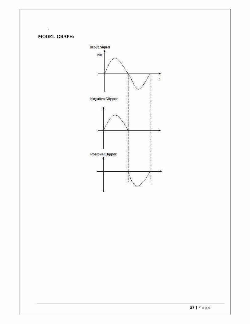
THEORY:
The Circuit which removes or clips a portion of the input signal either +ve or -ve side
without distortion in the remaining part of the input signal is known as ‘clipper’. The clipper
circuit is also called as ‘slicers’. In case of +ve clipper, the –ve half cycle is retained or
appearing in the output and –ve clipper the +ve half cycle will be appearing in the output.
57 | P a g e
.
MODEL GRAPH:

58 | P a g e
PROCEDURE:
For Positive and Negative clippers
1. The connections are made as per the circuit diagram.
2. The ouput will be appearing in CRO .
3. The output voltage , TON (+ve cycle) and TOff are noted down.
4. Amplitude of the output signal is noted down.
5. I/p is verified with O/p and the waveforms are drawn.
6. The diode connection is reversed and the same procedure is repeated for –ve
clipper
RESULT:
The circuits for Positive and Negative clippers are constructed and the outputs are
verified.
59 | P a g e
FG CRO, CH 1 CRO, CH 2
FG CRO, CH 1 CRO, CH 2
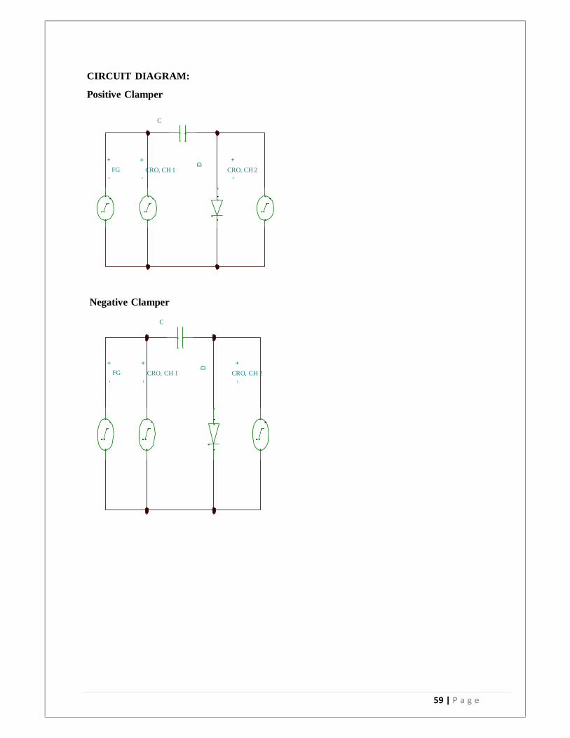
CIRCUIT DIAGRAM:
Positive Clamper
C
Negative Clamper
C
- +
-
+
- +
-
+
D
D
- +
-
+
60 | P a g e
POSITIVE AND NEGATIVE CLAMPERS
EX.NO: 15 DATE:
AIM:
To Construct and Test Positive Clamper / Negative Clamper using discrete
components, MULTISIM and ELVIS.
COMPONENTS & EQUIPMENTS REQUIRED:
S.No APPARATUS RANGE QUANTITY
1 P-N Jn diode IN 4007 1
2 Resistor 220 /1KΩ 1
3 Capacitor 100 F/1 F 1
4 Transformer 230/(12-0-12) V 1
5 Bread board - 1
6 Connecting wires - few
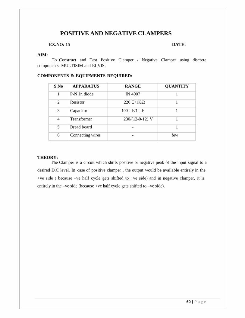
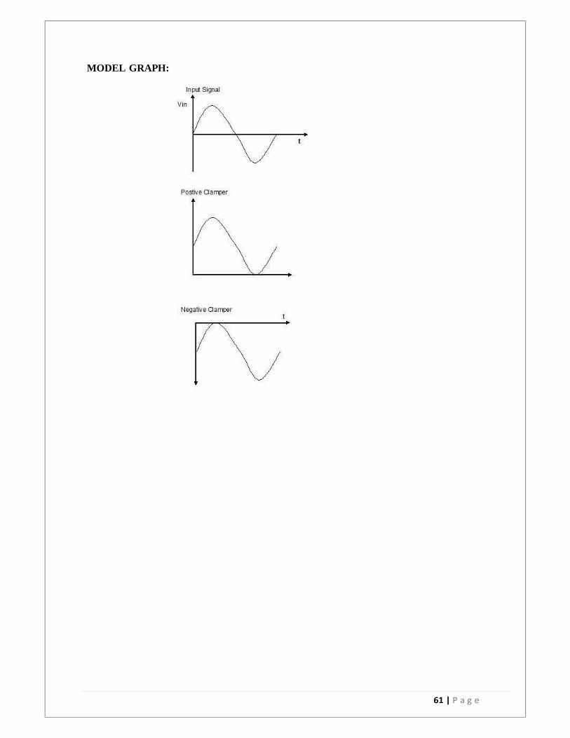
THEORY: The Clamper is a circuit which shifts positive or negative peak of the input signal to a
desired D.C level. In case of positive clamper , the output would be available entirely in the
+ve side ( because –ve half cycle gets shifted to +ve side) and in negative clamper, it is
entirely in the –ve side (because +ve half cycle gets shifted to –ve side).
61 | P a g e
MODEL GRAPH:

62 | P a g e
PROCEDURE:
For Positive and Negative Clampers -
1. The connections are made as per the circuit diagram.
2. The ouput will be appearing in CRO .
3. The output voltage , TON (+ve cycle) and TOff are noted down.
4. Amplitude of the output signal is noted down.
5. I/p is verified with O/p and the waveforms are drawn.
6. The diode connection is reversed and the same procedure is repeated for negative
clamper.
RESULT:
The circuits for Positive and Negative clamper are constructed and the outputs are
verified.

63 | P a g e
CIRCUIT DIAGRAM:
MODEL GRAPH:
64 | P a g e
CHARACTERISTICS OF BJT IN CB CONFIGURATION
EX.NO: 16 DATE:
AIM:
To plot the input and output characteristics of a Bipolar Junction Transistor (BJT) in
Common Base (CB) configuration using discrete Components, MULTISIM and ELVIS
COMPONENTS & EQUIPMENTS REQUIRED:
S.NO APPARATUS RANGE QUANTITY
1 RPS (0-30)V 2
2 Resistor 1KΩ 2
3 DC Voltmeter (0-30)V 1
4 DC Voltmeter (0-10)V 1
5 DC Ammeter (0-500)µA 1
6 DC Ammeter (0-30)mA 1
7 BJT BC54170/7BC 1
8 Breadboard - 1
9 Connecting wires - Few
THEORY:
The input is applied between e m i t t e r a n d b a s e a n d o u t p u t i s t a k e n from
the collector and base. Here, base of the transistor is common to both input and output
circuits and hence the name common base (CB) configuration. Regardless of circuit
configuration, the base emitter junction is always forward biased while the collector-base
junction is always reverse biased, to operate transistor in active region.

65 | P a g e
TABULATION:
Input Characteristics
VCB =
Sl.N VS (volt) VEB (volt) IE ( A)
Output Characteristics IE =
Sl.NO VS (VOLTS) VCB (VOLTS) IC (mA)
CALCULATIONS:

66 | P a g e
PROCEDURE:
Input Characteristics
1. Connections are made as per the circuit diagram.
2. The output voltage VCE is kept constant.
3. By varying the input voltage VBE , the corresponding input currents IB are noted down
4. A graph is plotted between VBE and IB.
5. The inverse slope of the curve gives forward input resistance.
Output Characteristics
1. Connections are made as per the circuit diagram.
2. The input current IB is kept constant.
3. By varying the output voltage VCE, the corresponding output current IC is noted down.
4. A graph is plotted between VCE and IC .
5. The inverse slope of the curve gives forward output resistance
RESULT:
The input and output characteristics of the transistor in CB mode are drawn and the
input and output resistances are calculated.
Input resistance =
Output resistance =
67 | P a g e
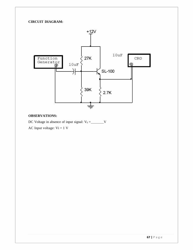
CIRCUIT DIAGRAM:
OBSERVATIONS:
DC Voltage in absence of input signal: VE = V
AC Input voltage: Vi = 1 V
68 | P a g e
EMITTER FOLLOWER-CC AMPLIFIER
EX.NO: 17 DATE:
AIM:
To observe input-output waveforms of common collector (CC) amplifier. To measure gain of
amplifier at different frequencies and plot frequency response using MULTISIM and ELVIS.
COMPONENTS & EQUIPMENTS REQUIRED:
S.No APPARATUS RANGE QUANTITY
1 CRO (0-30)MHz 1
2. Function Generator (0-3)MHz 1
3 Resistor 27K,2.7K,39K 1
4 Capacitor 10F 1
5 Transistor SL100 1
7 Regulated Power Supply (0-30)V 1
8 Bread board - 1
9 Connecting wires - Few
THEORY:
The common collector (CC) amplifier is also known as emitter follower. It is used as a current
amplifier. Voltage gain of CC amplifier is less than unity while current gain is (β+1). CC
amplifier has high input impedance and low output impedance. There is no phase reversal
between input and output.
PROCEDURE:
1. Measure Emitter voltage in absence of input AC signal.
2. Connect function generator at the input of the amplifier circuit.
3. Set input voltage 1V and frequency 100 Hz.
4. Connect CRO at the output of the amplifier circuit.
5. Observe output signal and measure output voltage
6. Draw input and output signal
RESULT:
Thus the input-output waveforms of common collector (CC) amplifier are verified.

69 | P a g e
CIRCUIT DIAGRAM:
CB configuration circuit using npn transistor
CE configuration circuit using npn transistor
70 | P a g e
TRANSISTOR BIASING USING ELVIS
EX.NO: 18 DATE:
AIM:
To study the characteristics of Bipolar Junction Transistor (BJT ) biasing using ELVIS and to
determine the characteristic curves (CB-Common Base, CE- Common Emitter) for the BJT.
COMPONENTS & EQUIPMENTS REQUIRED:
S.No APPARATUS RANGE QUANTITY
1 NI ELVIS - 1
2 Resistor 1K,27K,500 1
3 Transistor 2N3904 1
4 Regulated Power Supply (0-30)V 1
5 Bread board - 1
6 Connecting wires - Few
THEORY:
The bipolar junction transistor (BJT) can be modeled as a current controlled current source. As
an aid in visualizing the current/voltage relationships and transistor operation, a family of static
characteristics plots of collector current versus collector-base voltage for several values of
emitter current are plotted. This constitute the CB (Common Base) Collector characteristics. The
CE(Common Emitter) Collector characteristics constitute a family of static characteristics plots
of collector current versus collector-emitter voltage for several values of base current.
These curves can be used to calculate the large signal current gain βDC (or hFE) and the small
signal current gain, βAC(or hfe). These values are in general calculated for a given bias point ICQ,
VCEQ using the following equations:
βDC = ICQ / IBQ
βAC = | ICQ - ICQ’ |/| IBQ- IBQ’|
From this, one can see that a large signal gain depends only on the Q point and the small signal
gain depends only on small deviations around the Q point.
71 | P a g e
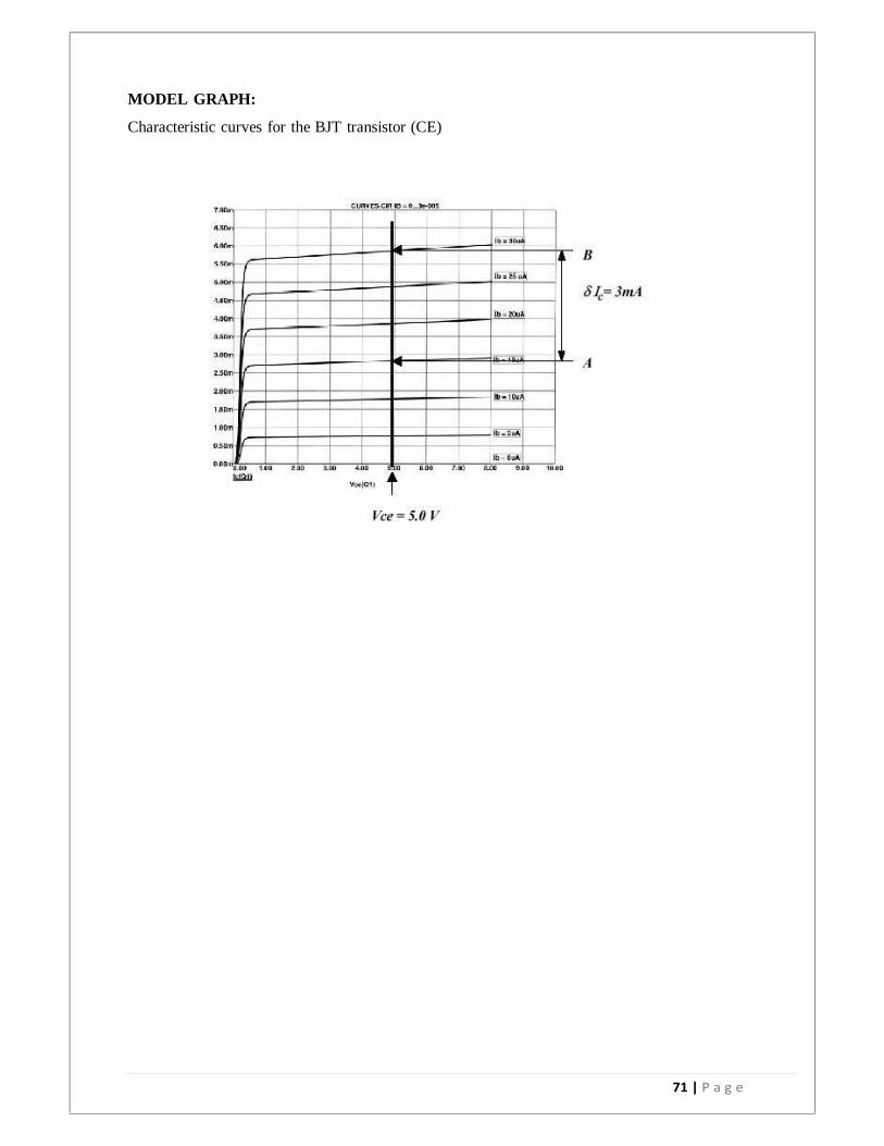
MODEL GRAPH:
Characteristic curves for the BJT transistor (CE)
72 | P a g e
PROCEDURE:
1) Transistor Common-Base Collector Characteristics
a) Connect the circuit shown in figure. Use Regulated Power Supply.
b) Vary Vcc from 0-10V in steps of 1 and measure (record) the collector current and the voltage
across collector and base .
c) Repeat the procedure for different values of IE (vary IE from 0-10mA in steps of 2mA).
d) Plot the V-I characteristics with Ic on Y-axis and Vcb on X-axis.
e) Calculate αDC and αAC from the curves.
2) Transistor Common-Emitter Collector Characteristics
a) Connect the circuit shown in figure.
b) Vary Vcc from 0-10V in steps of 1 and measure (record) the collector current and the voltage
across collector and emitter .
c) Repeat the procedure for different values of IB.(vary IB from 0-200µA in steps of 50µA).
d) Plot the V-I characteristics with Ic on Y-axis and VCE on X-axis. e) Calculate βDC and βAC
from the curves.
f) Calculate transconductance parameter gm.
3) Transistor Common-Emitter Base Characteristics
a) Vary VBB from 0-2V insteps of 0.2V, and measure the base current and the voltage across
base and the emitter.
b) Repeat the procedure for different values of VCE (0V, 0.1V, 1V, 2V)
c) Plot the V-I characteristics with IB(µA)on Y-axis and VBE on X-axis.
d) Calculate the base spreading resistance rb.
RESULT:
Thus the performance characteristics of Bipolar Junction Transistor (BJT ) biasing using
ELVIS was done successfully.