Organic electronic materials and devices for neuromorphic ...
40
1 Perspective: Organic electronic materials and devices for neuromorphic engineering Sébastien Pecqueur a , Dominique Vuillaume a , Fabien Alibart a,b,* a : Institut of Electronic, Microelectronic and Nanotechnology, Centre National de la Recherche Scientifique, University of Lille, Villeneuve d’Ascq, France b : Laboratoire Nanotechnologie et Nanosystèmes, Centre National de la Recherche Scientifique, Sherbrooke, QC, Canada *: corresponding author, [email protected]‐lille1.fr Abstract: Neuromorphic computing and engineering has been the focus of intense research efforts that have been intensified recently by the mutation of Information and Communication Technologies (ICT). In fact, new computing solutions and new hardware platforms are expected to emerge to answer to the new needs and challenges of our societies. In this revolution, lots of candidates’ technologies are explored and will require leveraging of the pro and cons. In this perspective paper belonging to the special issue on neuromorphic engineering of Journal of Applied Physics, we focus on the current achievements in the field of organic electronics and the potentialities and specificities of this research field. We highlight how unique material features available through organic materials can be used to engineer useful and promising bio‐inspired devices and circuits. We also discuss about the opportunities that organic electronic are offering for future research directions in the neuromorphic engineering field.
-
Upload
khangminh22 -
Category
Documents
-
view
0 -
download
0
Transcript of Organic electronic materials and devices for neuromorphic ...

1
Perspective:Organicelectronicmaterialsanddevicesfor
neuromorphicengineering
SébastienPecqueura,DominiqueVuillaumea,FabienAlibarta,b,*
a: Institut of Electronic, Microelectronic and Nanotechnology, Centre National de la
RechercheScientifique,UniversityofLille,Villeneuved’Ascq,France
b: Laboratoire Nanotechnologie et Nanosystèmes, Centre National de la Recherche
Scientifique,Sherbrooke,QC,Canada
*:correspondingauthor,[email protected]‐lille1.fr
Abstract:
Neuromorphiccomputingandengineeringhasbeenthefocusofintenseresearchefforts
thathavebeenintensifiedrecentlybythemutationofInformationandCommunication
Technologies(ICT). In fact,newcomputingsolutionsandnewhardwareplatformsare
expectedtoemergetoanswertothenewneedsandchallengesofoursocieties.Inthis
revolution, lotsofcandidates’ technologiesareexploredandwill require leveragingof
the pro and cons. In this perspective paper belonging to the special issue on
neuromorphic engineering of Journal of Applied Physics, we focus on the current
achievementsinthefieldoforganicelectronicsandthepotentialitiesandspecificitiesof
thisresearchfield.Wehighlighthowuniquematerialfeaturesavailablethroughorganic
materials can be used to engineer useful and promising bio‐inspired devices and
circuits.Wealsodiscussabouttheopportunitiesthatorganicelectronicareofferingfor
future research directions in the neuromorphic engineering field.

2
1‐Introduction
While the CMOS technologies are reaching physical limitations in terms of
performances,newsolutionsareexpectedtoemergeinthecomingyearstosustainthe
development of information and communication technologies (ICT). This tendency
represents a real opportunity to shift and explore new computing approaches that
wouldprovidenotonlybetterperformances,butmoreadaptedsolutions todealwith
the new needs of our societies. These new requirements should provide solutions to
numerousbig challenges amongwhich energy limitations constraints,management of
the high amount of heterogeneous data generated, massive parallelism and
heterogeneity of the communication network and of the interconnected electronic
devices (i.e. IoT) that are not coped easily by conventional machines. One of the
directionthatcouldpotentiallyanswersomeofthesechallengeswouldbetoreproduce
concepts and features observed in the brain: this extremely low power computing
engine is perfectly adapted todealwith heterogeneousdata suchas sound, vision, or
other sensory‐like signals thatwe recordandanalyze intensively inoureveryday life.
Furthermore, its plasticity and ability to adapt and learn make this object extremely
resilient to changing environments and operating conditions that would be very
appealing for themanagement of the complex network of devices constituting ICT of
tomorrow.
This approach should not only be limited to reverse‐engineering of the brain or bio‐
mimetism (which corresponds to reproducing with the highest precision some
biological features observed in biological systems by engineering), nor to map in
hardware machine learning algorithms that have proven their efficiency for image

3
classificationorothermachinelearningapplications.Itcouldbeextendedtoabroader
bio‐inspiredapproachthattargetstheexplorationoffeaturesorconceptsofinterestfor
computing purposes and finding some material implementation with emerging
technologies.
Neuromorphic engineering and computing, a term coined by CarverMead in the 80s,
represents the foundation for this direction.1 This concept was initially based on the
analogy between ions flux across the cell’s membrane and the CMOS transistor’s
transconductance,andhasbeenusedfortheimplementationofthefirstCMOSneuron.
Onekeyaspectofneuromorphicengineeringistodeeplyrelyonthedevicephysicsasa
computational primitive to build complex computing systems. While neuromorphic
engineering has been mostly implemented with standard CMOS technologies (so far
leading tobio‐inspired sensors and neural circuits),2,3 the field has recently benefited
fromtheemergenceofnewmaterialsanddevicesthathaveprovidednewopportunities
for neuromorphic engineers.Notably, pushedby the drastic requirements in terms of
memorydensity, resistivememory‐ormemristivedevices ‐havebeenenvisionedfor
implementing the synaptic weight connection between neurons.4 More advanced
utilization, closer to biological behavior, capitalized on thememory device physics to
realize very efficiently and locally learning rules observed in biology such as, for
instance,SpikeTimingDependentPlasticity(STDP).5‐7Morerecently,nanoscaledevices
have been also proposed to implement neuron’s building block.8‐10 Note that
neuromorphic engineering with emerging technologies is now going beyond single
neuromorphic devices and first neuromorphic circuits based on emerging nanoscale
deviceshavebeensuccessfullydemonstrated.11,12

4
Mostof thecurrentapproachesshare thebasicprincipleofusingelectronicprocesses
obtained by various devices engineering routes to mimic biological processes.
Nevertheless, biological systems and circuits issued from microelectronic are
intrinsicallyverydifferentanditisnotclearwhetherstandardelectronicplatformswill
be ideal candidates for neuromorphic implementations. In fact, devices and circuits
issued from microelectronic have been optimized for serial data transmission and
sequential logic applicationswhere ON/OFF switching ratio, speed and reliability are
majorconstraintswhileneuromorphicplatformrelaxtheserequirements(i.e.biological
computingengineshave intrinsically lowsignal tonoiseratio,slowsignalpropagation
and are fault/variation tolerant). As an interesting alternative to silicon‐based
technologies, this perspective paper proposes to emphasize on organicmaterials and
devicesaspotentialcandidatesforneuromorphicengineering.First,thesematerialsand
devicesarerecognizedtobeveryversatileengineeringplatforms:thesoftengineering
and bottom‐up routes used to synthetize and fabricate them can lead to a very large
panelofelectronicpropertiesrelevantforneuromorphicengineering.Secondly,organic
materials and devices can gather both electronic and ionic species as mobile charge
carriers. In suchsystems,electronicand ionicprocessescanbecoupledvianumerous
basic physical interactions, from electrostatic charge polarization to redox charge
transfer. These fundamental properties make organic iono‐electronic systems very
exciting candidates for implementing bio‐inspired concepts and could offer a new
toolbox forneuromorphicengineering.Wewillpresenthere fewof thebasicmaterial
properties that have been used for neuromorphic purposes. These propertieswill be
discussed in the light of selected examples that have been proposed recently for
neuromorphicimplementation.Finally,wewilldiscusstheveryunder‐lookeddirection

5
of material and device integration at the circuit and system level offered by organic
materialprocessingandwillhypothesizeontheperspectivesthattheyareoffering.
2‐OrganicMaterialsandDevicesinNeuromorphicEngineering
Theaimofneuromorphicengineeringatthemateriallevelistofindmediawhere
informationcarriersaretransportedinawaythattheymayenablesimilarmechanisms
ruling the information transport processes in biological media. From a very general
viewpoint, various biological features not available in standard electronics can be
highlighted. (i)Duality: In the synaptic cleft between two neurons, neurotransmitter
molecules and ions are both information carriers: neurotransmitters are a family of
chemical carriers confined in thesynapses,while ionsarechargedspeciesdelocalized
across the neural network via the electrolytic medium and cytoplasm. (ii) Time
Dependency: Transmission of signals between cells through synapses is largely
dynamical. For example, neurotransmitters are responsible for important time
dependencyofthetransmittedsignalscharging/dischargingofthepre‐synapticvesicles
and post‐synaptic receptors with different kinetically‐controlled physicochemical
processes. (iii) Chemicaldiversity: The distribution in physicochemical properties of
thedifferentanions,cationsandmoleculesmakesbiologicalcomputing’nodesacross‐
point of different vectors of information, enabling selective processes necessary to
interfacetheirrichenvironment:forsensingexogenousinformationortransducingitto
thebody.Inthatscope,organicelectronicmaterialshaveshownoverthepasttenyears
greatpromisesinemulatingthesepropertiesandcontinuenowadaystobio‐inspireus.
Following the example of synaptic plasticity, we illustrate how organicmaterials and
deviceshavebeenusedforneuromorphicengineeringandhowmorecouldbeexpected
inthisdirection.

6
2.1.Small‐moleculeandallotropic‐carbonorganicsemiconductorsmaterials.
One great advantage of organic semiconductors is the possibility to add new
functionalitiesby integratingdifferentmaterials via softprocesseswithoutdestroying
their electronic transport properties. We present in this section examples of such
material hybridization that have led to interesting neuromorphic applications when
variouselectronicmechanismsareadvantageouslycoupledtogether.
In2010,Alibartetal.demonstratedhowtousechargetrapping/detrappingtodesignan
organicSynapstor(synapsetransistor)mimickingthedynamicplasticityofabiological
synapse(figure1).13ThisdeviceisalsocalledNOMFET(NanoparticleOrganicMemory
Field Effect Transistor) and combines in a single structure both amemory effect (by
charge carrier trapping in nanoparticles) and a transistor effect (as the channel
conductance is field‐effect modulated). This device (which is memristor‐like) mimics
short‐termplasticity(STP),13andSTDP:7twofunctionsatthebasisoflearningprocesses
(Fig. 1).A compactmodelwasdeveloped,14 andanassociativememory,which canbe
trainedtopresentaPavlovianresponse,wasdemonstrated.15Althoughthepresenceof
the gold nanoparticles affects the crystallinity of the pentacene semiconductor, the
optimizedmobility for the functionalbiomimeticdevices can reproductively reach10‐
1cm²/V‐1·s‐1(higherthantheionicmobility inwater).16Anelectrolyte‐gatedversionof
this device was developed for biocompatible applications (EGOS: electrolyte‐gated
organic synapstor).17 STPwithauseful relativeamplitude (30‐50%of theaverageDC
current)wasdemonstratedatspikevoltagesaslowas50mV,withadynamicresponse
intherangeoftensofmsinaqueoussalinesolutionandcellculturemedium(leadingto
an energy of ca. pJ/spike). These EGOSs working at low voltages (e.g. 50mV) have

7
performances that open the potentiality to directly interface real neurons. Human
neuroblastoma stem cells successfully adhered, proliferated and differentiated into
neuronsontopoftheEGOSasmonitoredbyopticalmicroscopy.18
Figure1:(a)STP(adapted from[19])and(b)SDTP(adapted from[20])ofabiological
synapseand(c‐d)correspondingbehaviorfortheNOMFET(adaptedfrom[7,13]).
Carbon allotropes were also investigated as organic materials for neuromorphic
engineering: OG‐CNTFET (optically‐gated carbon‐nanotube field‐effect transistor) are
interesting since they are programmable (optically and electrically) with multiple
memory states.21‐23 OG‐CNTFET are made of carbon nanotube FETs (single CNT or
randomnetworkofCNTs)coveredbyaphoto‐conductingpolymer (e.g.P3OT,poly(3‐

8
octylthiophene‐2,5‐diyl))making themlight‐sensitiveandconferring theirnon‐volatile
memory behavior. These carbon‐nanotube‐based memory elements can be used as
artificial synapses and eight OG‐CNTFET, combined with conventional electronic
neurons, have been trained to perform Boolean logic functions using a supervised
learning algorithm.24 In a crossbar architecture, the OG‐CNTFET allowed an efficient
individual addressing (reduced crosstalk) by virtue of the development of a "gate
protectionprotocol"exploitingthespecificelectro‐opticalbehaviorofthesedevices.25
Thinfilmsofredoxmoleculescanalsobeusedforneuromorphicdevices.Y.P.Linetal.
have developed a non‐volatile nanoscale organic memristor based on electrografted
redox complexes (iron(II) tris–bipyridine complexwith diazonium grafting functions)
onmetalelectrodes.26Thesedevicesareprogrammablewithawiderangeofaccessible
intermediateconductivitystates.Theseauthorsexperimentallydemonstratedasimple
neuralnetworkcombining fourpairsoforganicmemristorsassynapses(andneurons
madeofconventionalelectronics)capableoflearningfunctions.
2.2.Electrolyte‐GatedSemiconductingPolymers
Polymersarewellestablishedmaterialsinmicroelectronicfabricationsincetheycanbe
chemically tuned for theirmicro/nano‐patterning on silicon: they are therefore good
candidates for technological hetero‐integration on CMOS. Also as organic electronic
materials, they offer more flexibility than small molecules to interface solvents for
solutionprocessingandliquidelectrolyte‐gating.Thepossibilitytointegrateelectrolytes
(as ion carriers)on topoforganic semiconductors (ashole/electroncarriers)without
damaging the one or the other offers the possibility to benefit of both charge carrier
processesinanall‐organicneuromorphicdevice.

9
To the best of our knowledge, the first report of an organic device for neuromorphic
systemwas proposed in 2005 by Erokhin etal.27 The devicewas based on anHCl p‐
doped polyaniline (PANI) conducting polymer interfaced with a LiClO4/poly(ethylene
oxide) (PEO) solid electrolyte.28 In this device, the kinetically limited process is
attributed to a Resistive/Capacitive (RC) internal circuit, correlated to the bulk
conductivity of the doped/dedoped‐polymer and the accumulation of ions at the
PANI/PEO interface.29,30 Thedopingof PANIwith stronger acids andbulkier counter‐
anionspromotes the repeatabilityof thedeviceperformanceswhile controlling itsRC
properties.31Morerecently,Deminetal.32usedthesedevicesasthesynapselayerofa
simple perceptron, which has learned using an error‐correction‐based algorithm
proposedbyRosenblattinitsseminalpaperonperceptron,33toimplementtheNANDor
NOR logic functions as simple examples of linearly separable tasks. Undoped hole
transporting polymers have also been tested such as poly(3‐hexylthiophene) P3HT,
showing paired‐pulse facilitation (PPF),34 and shows that the formation of water
channelsinthesolidelectrolyteplaysanimportantroleinthefunctioning.35
2.3.Iono‐electronicpolymers:mixelectronicandionicconductioninorganicmaterials
Amoreintimatecouplingbetweenionsandelectronscanbeobtainedwhentheir
interactionisnotlimitedattheinterfacebetweentwomaterialsbutcouldberealizein
the bulk. This option has been advantageously deployed to transduce ionic into
electronicsignals(andreciprocally)inavarietyoforganicelectronicmaterials.
Iono‐electronicpolymercanbeintimateblendsofchargedpolymers,suchasthe
well‐known poly(3,4‐ethylenedioxythiophene):poly(styrenesulfonate) (PEDOT:PSS).
The semiconducting PEDOT is a low oxidation potential polymer which
thermodynamicallyundergoin itsoxidizedstate inmoistair.36 InPEDOT:PSS,thePSS‐

10
negative charges are compensated by a positive charge (i.e. a hole) on the PEDOT
aromaticmoleculetorespectelectro‐neutrality.ThenegativechargesonPSS‐arefixed
while the positive charge on the PEDOT+ can easily be delocalized and contribute to
electronic transport. In addition, if some external mobile ions can penetrate into the
bulkofthePEDOT:PSS,thelocalelectronicconductivitywillbetunedbasedonthesame
electro‐neutralityprinciple (i.e. addingonemonovalentpositive ionbalancesonehole
extractedfromthePEDOTpolymerchains).Theabilitiesofthesematerialsanddevices
to gradually change their electrical conductivity upon ion/electron exchanges made
them promising materials for brain‐like circuitry that is in nature an "iontronics"
system.Lietal.usedPEDOT:PSSinarectifyingmemristorstructuretodemonstrateSTP,
long‐term plasticity (LTP), STDP and spike‐rate‐dependent plasticity (SRDP).37 It has
also been used with liquid‐electrolyte gating, showing time‐dependent paired‐pulse
depression (PPD).38 By substituting the PSS to poly(tetrahydrofuran) (PTHF), the
memorybecomeslessvolatile,39andpromotesLTP,40withPPDabouttentimesslower
than PEDOT:PSS systems.38 Based on PEDOT:PSS, another device structure named
ENODe(electrochemicalneuromorphicorganicdevice)wasrecentlyproposedasalow‐
voltageorganicsynapse.41ThedevicestructurefeaturestwoPEDOT:PSSelectrodes(one
partly reduced by a poly(ethylenimine) treatment separated by an electrolyte. Upon
applicationof pulse voltage on one of thePEDOT:PSS electrode (used aspre‐synaptic
input), cation exchange through the electrolyte modifies the conductivity of the
PEDOT:PSS/PEIfilmusedasthepost‐synapticoutput.Workingatalowvoltage(around
1mV)andalowenergy(10pJ),thisdeviceshowednon‐volatility,long‐termpotentiation
anddepressionwith500discretestateswithintheoperatingrange.
2.4.Perspectives

11
Onthefirstaspectabouttheinformationcarriers’duality,electrolyte‐interfacing
organic semiconductor systems can mimic biological synapses with electrons/holes
emulating the ions and ions emulating the neurotransmitters (Figure 2a). The slow
dynamicsassociatedto ion/electroninteractionarewelladaptedtoreproducevolatile
memory effects. This represents an advantage over other standard electronic
technologies,inparticularRRAMorOxRAMsystemsthathavebeenoptimizedfornon‐
volatilememoryapplications.42Whilememristivedeviceshavebeenmostlyconsidered
for their analogprogrammabilitypotential (i.e. implementingadvantageously synaptic
weight), such volatilemechanisms are only obtained in diffusivememristors43,44with
only little possibilities to be adjusted (i.e. unstability in nanoscale filaments).
Advantageously, volatility level appears to be largely tunable in organic system. In
addition, studies performed with solid electrolytes such as PEO shows that these
platforms can be downscaled for high‐density development,45,46 while studies
performedwithwater as an electrolyte shows their potential application to interface
biology.47‐49
The time‐dependency of signal transmission and propagation observed in
biologycanalsobeadvantageouslyreproducedwithorganicsystems.Forinstance,ionic
andelectronicproperties suchaschargemobility inelectrolyteormetal, respectively,
arestronglydifferentandresult inverydifferentperformancesforsignalpropagation.
Consequently, implementingat thedevice levelbio‐realistic timeconstantobserved in
biology(suchasmembranetimeconstantinneuralcells,orneurotransmitterdynamics
at the synaptic cleft) requires large capacitances in thepurelyelectronicmediumand
are a severe limitation in terms of circuit design. In particular, the interplay between
ionic transient currents and electronic steady‐states allows the tuning of the signal
propagation dynamics,50 which influences all the plasticity‐related elementary

12
mechanisms of the artificial synapse: the interfacing of the electrolyte with the
semiconductor is therefore a key parameter. Iono‐electronic polymers have the
advantagetobehydrophiliccomparedtoneutralpolymersandallowtheirswelling in
thepresenceofwater,51promotingtheioncharge/dischargeofthebulkofthematerial
rather than the top surface.52 The bulk capacitance of these electrolyte‐interfacing
materials is non‐ideal and relates to constant‐phase‐elements impedances of porous
systems,which can be emulatedwith infinite numbers of series/parallel RC elements
(Figure2b).53,54Analogously, thesenon‐ideal impedancesarealsoruling thediffusion‐
control existing at the cellular membrane.55‐57 Developing further organic
semiconductor promoting the ion transport at nanoscale in the bulk of the electrical
material is attractive to emulate the non‐ideality of the impedance ruling the whole
time‐dependency in theelectrochemicalsignal response.Other ionomersareofrecent
interest in organic electrochemical transistors such as conjugated polyelectrolytes
(either self‐doped or intrinsic)58‐60. Also several works are currently promoting the
conception of neutral semiconducting polymer with hydrophilic properties, by the
introductionofglycolchains.61,62
Finally, at the chemicaldiversity level, organic electronics could offer a well‐
adapted platform to couple various functionalities at the device level. Coupling
neuromorphic sensing, transduction and computing at the hardware level is still not
extensively investigated, although biomimetic sensing/transduction platforms are in
need for neuromorphic data analysis of pattern‐recognition based applications.63,64
Especially for input/output layers, sensing/transduction of exogenous information
(light, mechanical deformation, chemical) to/from ionic action potentials requires
specific materials for coupling the neural information transport properties to the
desiredsensed/transducedphysical information.Organicsemiconductormaterialscan

13
show fluorescence and phosphorescence,65 promoting a direct coupling between the
material electrical properties and a specific wavelength range of emitted light (as
organic light‐emitted diodes)66,67, or absorbed one (as organic photodiodes).68‐70 The
photo‐transduction associated to the modification of the rectification ratio of
photodiodes by light canmodulate thematerial electrical conduction under reversed
bias, mimicking retinal photoreceptor cells. Organic semiconductors are also
mechanicallystable71,andsemiconductingiono‐electronicpolymerssystemscanalsobe
electroactive and transduce by electrical stimuli as low as 2V to morphological
changes.72 Reversibly, they can also sense mechanical deformations (as cutaneous
nerves or cochlea’s hair cells), modifying the electrical properties of electronic skins
sensors.73,74 Finally, electrical properties of organic semiconductors can also be
molecularlymodulated,gatingtheelectronicstateof thechannel fromnon‐conducting
(inhibition) to conducting (excitation).Molecular‐gating of the organic semiconductor
conductivity can be done either directly in the material by doping with molecularly‐
specific strong electron acceptors (p‐type) or donors (n‐type),75,76 or indirectly by
performances modification of an external gate with specific electroactive agents
containedintheelectrolyte.77,78Theintegrationofsuchmolecularagentsinthematerial
(either thesemiconductoror theelectrolyte),modulating theconductivityaccordingly
to their chemistry, provides a versatile mean to incorporate both performance
variabilityandselectivitynecessarytointegratemultipleprocessesatthenetworklevel
usingasingleelectronictechnology.

14
Figure2:(a)Analogybetweenabiologicalsynapseandorganic‐electrochemicalsynapse.
(b)DeLevie infinite transmission line impedancemodel forporouselectrodewith redox
(GerischerImpedance)orwithoutredox(WarburgImpedance)reaction.
3‐Circuitsandsystemsbasedonorganicprocesses
3.1‐Generalconsiderationsandrecentachievements
One of the important challenges that neuromorphic engineering is facing is to bring
elementary devices (or basic building blocks) at the circuit and system level. Some
importantaspectsoftheproblemare:(i)Toreproducethehighparallelismofneural
network in hardware. For example, conventional memory structures are mostly
accessed sequentiallywhen onewould deeply benefit from a parallel and distributed
memoryarchitecturetoemulatesynapticoperationsbetweencells.Potentialsolutions
tothischallengehavebeenconsideredbasedontheideaofpassivecrossbararrayswith
resistive memories. But, scaling of this approach seems limited due to physical
limitation in termsofenergycostandengineering limitationswhenone tries tomove
charges over long andpassivemetallicwires79. (ii)Toreproducethecombinationof
bothlocalandglobaleffectsobservedinbiology.Someprocessesarehighlylocalsuch

15
assynapticplasticityprocesses(i.e.SpikeTimingDependentPlasticity,forexample)and
wouldbenefitfromembeddedplasticfeaturesascloseaspossibletothememorypoint.
Some others such as reinforcement learning (i.e. associated to processes such as
dopamine delivery in the brain) or homeostasis are global effects affecting large
populations of cells andwould benefit from amore global circuitry such as a central
processingunit.Thislateraspectissomehowinoppositionwiththeideaofdistributed
computing units and locality. (iii) To reproduce the complex wiring between
populationsofcellsinhardware.Infact,iftheissueoffan‐in/fan‐outcouldbesolved,
one remaining question is to implement in hardware the ability of cells to transmit
information on different length scale. For instance, if one neuron projects on 10000
neuronsonaverage, the targetpopulationof thisprojectionvariesdeeply fromcell to
cellandinvolvesboth“hard‐wiring”(i.e.neuraltopologythatpre‐existbeforelearning)
and “plastic‐wiring” (i.e. wiring between cells resulting from different learning
experiences). Since this complexwiring is inprinciplenotknownbefore learning, the
conventional top‐down technological approach is to oversized the interconnection
between cells (i.e. allow for the highest degree of interconnection between cells and
restrict it after learning) or to make arbitrary decision on a reasonable degree of
interconnection and a pre‐defined population of cells that will be allowed to
communicate between each other. The first aspect is somehow illustrated by the
conceptofpassivecrossbararraysandthesecondbythemostadvancedneuromorphic
implementations such as True North80 or Spinnaker81 where Address Event
Representation(AER)isusedtoemulateparallelcommunicationbetweenpopulations.
3.2.Organicmaterialsfordendriticengineering

16
Passive crossbar arrays of resistive memory cross‐point are an elegant solution to
reproducethehighlevelofparallelismbetweencells4. Itcorrespondstoimplementing
withmetallicwirestheaxono‐dendritictreeofbiologicalneuralcellsandtoimplement
the synaptic weight with memory cross‐point. In this approach, one challenge is to
minimizewires’resistanceinordertonothidethememoryelements’resistanceitself.79
Nevertheless, this approach neglects some important aspects at work in biological
networks such as dendritic computing.82 In fact, transmission speed along axons and
dendrites,localizationofthesynapticcleftalongthedendriticarborandtheirrespective
timingareusedas importantcomputing ingredientsbybiologicalcells.These features
canhardlybeimplementedwithpurelyelectronicconductorsorattheexpenseofheavy
overhead circuitry to implement the bio‐realistic time constant for example. Few
interestingpropositionshavebeenrecentlypublishedinthefieldoforganicelectronics
that could offer new perspectives for this particular feature. Xu et al. proposed to
implement the interconnectingwires (figure 3a)with conducting organicmaterials.83
Thisapproach isof interest for theeaseof implementationof theconductivewiresby
inkjet printing but also lead to interesting dendritic properties. So far, the authors
demonstrated PPF and STDP on the organic nanowire/synapse system. Note that the
materialsystemisanorganic/electrolytedevice innatureandthat thecombinationof
both ionic and electronic dynamics results in bio‐realistic temporal features at the
device level.An interestingperspectivewouldbe toextendtheanalogywithdendritic
processesatworkinbiologicalcells.
Along the idea of dendritic computing features, other works have reported the
possibilitytouseorganicmaterialsforimplementingdendriticconnections.Workfrom
Malliarasetal.proposedtoimplementdendriteswithPEDOT:PSSmaterials.84Thisiono‐
electronicpolymerwasusedtodemonstrateorientationselectivityalongalongPEDOT
17
linewithmultiplegates localizedalongthewire inanelectrolyticenvironment(figure
3c).Interestingly,timelageffectwasdemonstratedtodependonthegatelocationanda
direct analogy with temporal integration along the dendrites can be seen in this
experiment. Temporal features were the result of both the ionic dynamics in the
electrolyteandtheelectronicpropertiesofthePEDOT:PSSmaterial.
A third material system based on Indium Zinc Oxide (IZO) transistor electrolitically
gatedwithachitosanmembranedemonstratesdendritic features (figure3b).85 In this
work thechitosan layer isusedasaprotonconductormaterialandcanbe thoughtas
equivalenttoanartificialdendrite.Theorganicionicconductor(chitosan)isthenused
to implement temporal features observed in biological dendrites with multiple gates
implementingthepre‐neuroninput.
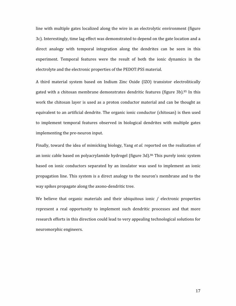
Finally,towardtheideaofmimickingbiology,Yangetal.reportedontherealizationof
anioniccablebasedonpolyacrylamidehydrogel(figure3d).86Thispurelyionicsystem
based on ionic conductors separated by an insulatorwas used to implement an ionic
propagationline.Thissystemisadirectanalogytotheneuron’smembraneandtothe
wayspikespropagatealongtheaxono‐dendritictree.
We believe that organic materials and their ubiquitous ionic / electronic properties
represent a real opportunity to implement such dendritic processes and that more
researcheffortsinthisdirectioncouldleadtoveryappealingtechnologicalsolutionsfor
neuromorphicengineers.

18
c)
a) b)
+ + +
+ + +
+ + +
+ + +
_ _ _
_ _ _ _ _ _
_ _ _
_ _ _ + + + + + + + + +
_ _ _ _ _ _
Ionic conductor
Ionic conductor
Dielectric
i(x,t)
v(x,t)
Electrical double layer
x
i(x,t)
Input port
Output port
Z
Electrode
d)
Figure3:(a)Organicdendritesandsynapsesrealizedby inkjetprintingoforganiccore‐
sheathnanowire(from [83]). (b)Emulationofdendriticpropagationof signalswith IZO
transistorand chitosan ionicmembrane (adapted from [85]). (c)Orientation selectivity
withdendritic‐likeorganicelectrochemicaltransistors(adaptedfrom[84]).(d)Conceptof
ioniccable(adaptedfrom[86]).
3.3. From local to global processes: mix ionic/electronic conductors with global
electrolyte
Asmentionpreviously,learninginbiologycanresultfromdifferentspatialscales.From
purely local event induced by chemical processes happening at the synaptic cleft, to
extendedcontributionsuchasthetri‐partitesynapsethatinvolvethecontributionofthe
glial cells into synaptic potentiation (note that glial cells can extend along multiple
neuronsandprovidesubsequentlyanadditional interconnectionbetween thesecells),

19
to reinforcement learningwhere the overall synaptic learning can be influenced by a
globalmarkersuchasdopamineconcentration.Thesemechanismsarepossiblethanks
tothemultiplecarriersofinformationthatareusedinbiologicalengines(variousions
and chemicals) and that are hardly reproduce with single data carriers in standard
electronics. Gkoupidenis et al. published an interesting solution toward this goal
recently.87 The proposed system was composed of a passive matrix of OECTs
interconnectedbymetallicwiresimplementingthe“electronic”partofthesystemandof
aglobalelectrolyteusedtogatetheOECTdevicesimplementingthe“ionic”partofthe
system (figure 4a and 4b). Local synaptic effects can potentially be implemented on
single OECT (see previous sections) while global effects are implemented via the
electrolyteandtheioniccarriersof information.Integratingagridof4x4OECTsgated
bythesameelectrolyte, theseauthorsdemonstratedthat theycangloballycontrolthe
behavior of the OECTs in the array, a behavior that resembles homeoplasticity
phenomena of the neural environment. They also show that OECTs can communicate
thoughthecommonelectrolyte,i.e.aninputsignalsenttooneOECTisalsodetectedbya
neighboringoneinthenetwork.
Alongthisline,weproposerecentlyaconceptofspatialreservoirwithOECTsensors.88
In this system (figure 4c‐e), the connectivity through the electrolyte was used to
transmit the input signal froma global gate to anetworkof12OECTs.Thanks to the
electropolymerization of the p‐type iono‐electronic polymer, each individual sensing
element presented a many‐fold variability in time response, charge/discharge‐
symmetry,channelconductanceandtransconductance,affectingtheoutputimageofthe
gate input signal.We demonstrated in this work that non‐trivial binary classification
taskscanberealizedoutof thissystem:thesystemhasbeenable todiscriminate two
differentfrequency‐modulatedvoltagepulsespatternsinjectedfromthegate,witherror

20
rates controlled by the number of training vectors, the number of OECTs and their
variabilities.ShowingthatthemorethebetterintermsofnumberofOECTsandtraining
vectors,thisstudyalsounravelsthatanappropriatesetofarestrictednumberofOECTs
can systematically lead to an optimal recognition or not, depending on the individual
device properties (the relevant properties responsible for pattern recognition
performance of the network have not been quantitatively identified yet). Considering
therelationshipbetweenelectrolytenatureandthegatefield‐effectefficiency75,89,more
isexpectedinastudywhereafixedandperiodicalpatternwouldbeinjectedfromthe
gate and the electrolyte medium would be modified as an input: more complex
interactionbetweentheelectrolyteandOECTsuchassensitivitytovariousionicspecies,
sensitivitytoconcentrationcouldbeaddedintotheoverallsystem.

21
Figure 4: (a‐b) Global gating through the electrolyte of organic electrochemical
transistorsshowingbothlocalandglobaltenabilityofthedevices(adaptedfrom[87]).(c‐
d)Concept of spatial reservoir implementedwith electropolymerizedOECTs forpattern
classification(adaptedfrom[88])

22
3.4.Fromsynapticlearningtonetworkwiring.
As pointed out by J. Hawkins at IEDM2015,90 synapticweightingwith analogweight
suchasresistivememoryisinessencedifferentfromtheconceptofwiringobservedin
biology. The former corresponds to continuous evolution of the synaptic weight
betweentwovalues(theminandmaxconductanceofthememoryelement)whilethe
latercorrespondstoacontinuousevolutionofan“undisplayed”synapticstate.Inother
words, thepotential synapse thatwill result fromthegrowthofadendriticpathdoes
notcontributetocomputinguntil thesynapticconnectionisestablished.Nevertheless,
importantlearningandcomputingeventscanbeattributedtothisdendriticgrowth.One
couldexpectthatartificiallyreproducingthedendriticwiringthroughfixenetworksuch
as parallel crossbar topologies will miss important aspect of biological computing,
notablyintermsofenergyconsumptionsinceallweightsinthenetworkwillcontribute
topowerconsumption(evenifthereconductanceissmall)whileundisplayedsynaptic
element not. In addition, aging consideration should consider that if fix topology
network can be used to compensate to device aging (i.e. synaptic connections that
become inefficientare replacebynewones) to someextend (until enoughalternative
pathwayareavailable),thisapproachdoesnotsolvecompletelytheimportantabilityof
biologytoregeneratenewconnections.
3.5.Perspectivesforneuromorphic
Organicelectronicmaterialsofferalsobiomimeticperspectivesatthenetworklevelby
their fabrication processes (top‐down and bottom‐up), which could emulate the
morphologicalevolutionoftheneuralnetworkwhilepreservingthefunctionalityofthe
elementaryorganicelectronicelements.
23
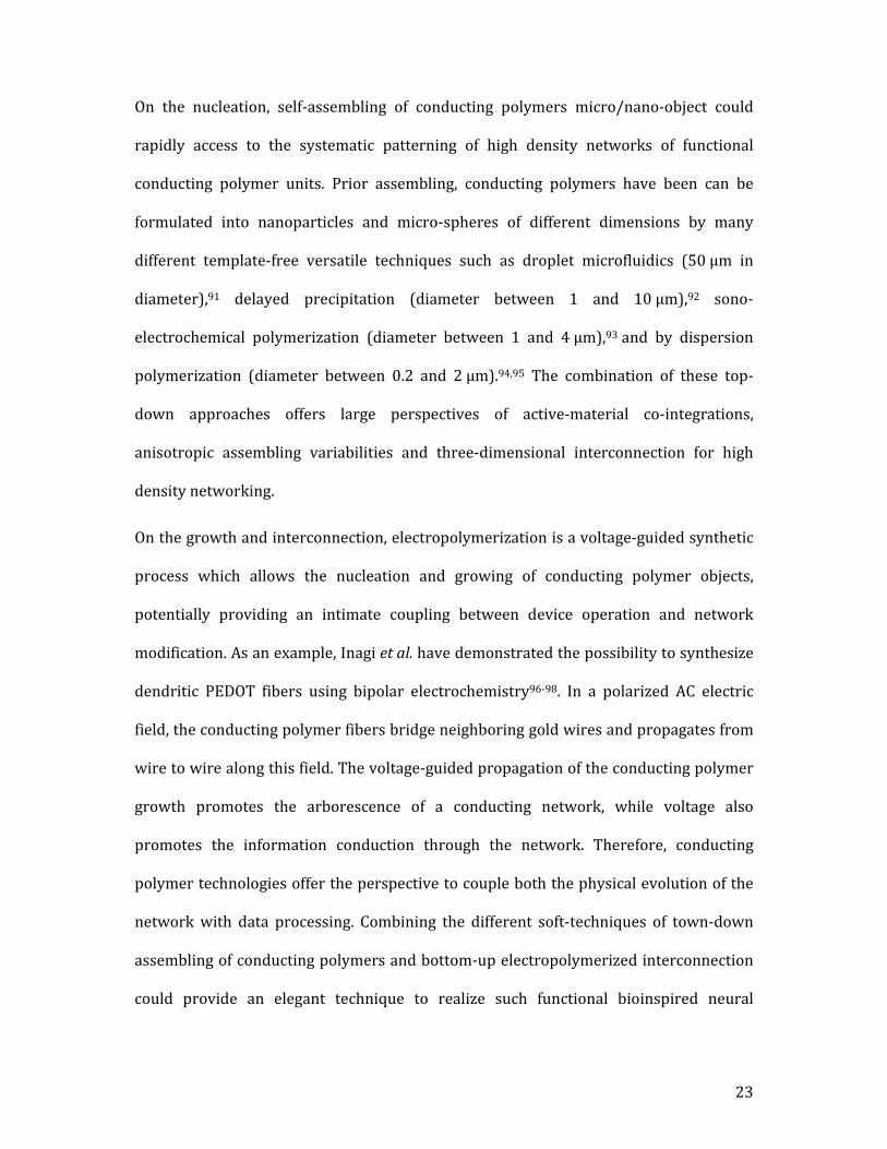
On the nucleation, self‐assembling of conducting polymers micro/nano‐object could
rapidly access to the systematic patterning of high density networks of functional
conducting polymer units. Prior assembling, conducting polymers have been can be
formulated into nanoparticles and micro‐spheres of different dimensions by many
different template‐free versatile techniques such as droplet microfluidics (50μm in
diameter),91 delayed precipitation (diameter between 1 and 10μm),92 sono‐
electrochemical polymerization (diameter between 1 and 4μm),93and by dispersion
polymerization (diameter between 0.2 and 2μm).94,95 The combination of these top‐
down approaches offers large perspectives of active‐material co‐integrations,
anisotropic assembling variabilities and three‐dimensional interconnection for high
densitynetworking.
Onthegrowthandinterconnection,electropolymerizationisavoltage‐guidedsynthetic
process which allows the nucleation and growing of conducting polymer objects,
potentially providing an intimate coupling between device operation and network
modification.Asanexample,Inagietal.havedemonstratedthepossibilitytosynthesize
dendritic PEDOT fibers using bipolar electrochemistry96‐98. In a polarized AC electric
field,theconductingpolymerfibersbridgeneighboringgoldwiresandpropagatesfrom
wiretowirealongthisfield.Thevoltage‐guidedpropagationoftheconductingpolymer
growth promotes the arborescence of a conducting network, while voltage also
promotes the information conduction through the network. Therefore, conducting
polymertechnologiesoffertheperspectivetocoupleboththephysicalevolutionofthe
networkwith data processing. Combining the different soft‐techniques of town‐down
assemblingofconductingpolymersandbottom‐upelectropolymerizedinterconnection
could provide an elegant technique to realize such functional bioinspired neural

24
network,99but also to have a coupling between network morphological change and
operation,necessarytomimiclong‐termmemoryatthenetworklevel.
a) b)
c) E=30.3 V.cm-1
E=30.3 V.cm-1
E=30.3 V.cm-1
25 s
29 s
10 s
Figure5:(a)Assemblingofconductingpolymermicrospheres(adaptedfrom[92]),scale
bar is5um. (b)DendriticPEDOT:PSS interconnection (adapted from [97]). (c)Electrical
interconnectionofmicrospheres(adaptedfrom[99]).
4‐Conclusion
Insummary,therecentresultsreviewedinthispaperhavedemonstratedthatorganic
materialsanddevicesarepronefortheimplementationofneuromorphicfunctions,not
only at the single device level, but also at the circuit level. Some perspectives are
discussed showing the possibility to improve these systems towards an increased
complexityintermsoffunctionsandcircuitconnectivity.Fromaverygeneralviewpoint,
table 1 points out the intrinsic properties of organic iono‐electronic materials and
inorganicsilicon‐basedtechnologies.Atthelightofthistable,thedifferentperspectives

25
frommaterials,devices,tosystemlevelforneuromorphicengineeringcanbeevaluated.
Sinceneuromorphicengineeringisstillanemergingcomputingparadigm,thequestion
ofthemostappropriatetechnologyisstillcompletelyopen.This laststatementshould
beofcoursebalancedby thevery importantcriterionof technologymaturity thatwill
enableneuromorphictechnologiestobetransferredtotheindustriallevel.
Biological hardware: • High impedance • Operating conditions: wet, low signal/
noise ratio, slow • Communication: Ionic, chemical • Computing: analog, parallel • organization: Bottom‐up
Conventionnal computer: • Low impedance • Operating conditions: dry, high S/N
ratio, fast • Communication: electronic • Computing: digital, serial • organization: Top‐down
Material
Device
System
Table1:Comparisonofthemainintrinsicpropertiesforbothorganicandinorganic
technologies.Thesepropertiescouldbethoughtinthelightofthemaincharacteristics
ofbiologicalcomputingsystems.
CMOS technology Organic ion/electronic technology
Biology
Operational environment
Dry (sealed packaged) Air / water stable Wet
Information carrier
electrons / holes electrons / holes / ions / chemicals
ions / chemicals
Mobility
(cm2
/(V.s)) 1‐10
3
(silicon) 10‐6
to 10 (electronic)
10‐4
to 10‐3
(ionic)
10‐3
(ionic)
Capacity (μF/cm2
) 1 (high‐k oxide with thickness of few nm) note: Capa. decreases
with thickness
500 (130 nm PEDOT film with volumic capacitance)
note: Capa. increases with thickness
1 (cell’s membrane)
Fabrication top‐down lithography top‐down lithography bottom‐up self assembling,
eletropolymerization
Bottom‐up

26
Acknowledgements.
PartsoftheworksreviewedherehavebeenfinanciallysupportedbytheEuropean
UnionprojectsNABAB(FP7‐FET‐FP7‐216777),SYMONE(FP7‐FET‐318597),I‐ONE
(FP7‐NMP‐280772),RECORD‐IT(H2020‐FET‐664786)andtheFrenchAgencyANR
projectSYNAPTOR(12BS0301001).

27
References:
1. C.Mead,ProceedingsoftheIEEE(1990),p.1629.
2. C.Bartolozzi,R.Benosman,K.Boahen,G.Cauwenberghs,T.Delbrück,G.Indiveri,
S.‐C.Liu,S.Furber,N.Imam,B.Linares‐Barranco,T.Serrano‐Gotarredona,K.
Meier,C.PoschandM.Valle,Neuromorphicsystems.(WileyEncyclopediaof
ElectricalandElectronicsEngineering,2016).
3. G.IndiveriandS.‐C.Liu,ProceedingsoftheIEEE(2018),p.1379‐.
4. D.B.Strukov,Nature476,403(2011).
5. S.H.Jo,T.Chang,I.Ebong,B.B.Bhadviya,P.MazumderandW.Lu,NanoLett.10,
1297(2010).
6. D.Kuzum,R.G.Jeyasingh,B.LeeandH.S.P.Wong,NanoLett.12,2179(2011).
7. F.Alibart,S.Pleutin,O.Bichler,C.Gamrat,T.Serrano‐Gotarredona,B.
Linares‐BarrancoandD.Vuillaume,Adv.Funct.Mater.22,609(2012).
8. J.Grollier,D.QuerliozandM.D.Stiles,ProceedingsoftheIEEE(2016),p.2024.
9. J.Torrejon,M.Riou,F.A.Araujo,S.Tsunegi,G.Khalsa,D.Querlioz,P.Bortolotti,V.
Cros,K.Yakushiji,A.Fukushima,H.Kubota,S.Yuasa,M.D.StilesandJ.Grollier,
Nature547,428(2017).
10. P.Stoliar,J.Tranchant,B.Corraze,E.Janod,M.‐P.Besland,F.Tesler,M.Rozenberg
andL.Cario,Adv.Funct.Mater.27,164740(2017).
11. M.Prezioso,F.Merrikh‐Bayat,B.D.Hoskins,G.C.Adam,K.K.LikharevandD.B.
Strukov,Nature521,61(2015).
12. G.W.Burr,R.M.Shelby,S.Sidler,C.DiNolfo,J.Jang,I.Boybat,R.S.Shenoy;P.
Narayanan,K.Viwani,E.U.Giacometti,B.N.KürdiandH.Hwang,IEEETrans.
ElectronDevices62,3498(2015).

28
13. F.Alibart,S.Pleutin,D.Guerin,C.Novembre,S.Lenfant,K.Lmimouni,C.Gamrat,
andD.Vuillaume,Adv.Funct.Mater.20,330(2010).
14. O.Bichler,W.Zhao,F.Alibart,S.Pleutin,D.VuillaumeandC.Gamrat,IEEETrans.
Electron.Dev.Soc.57,3115(2010).
15. O.Bichler,W.Zhao,F.Alibart,S.Pleutin,S.Lenfant,D.Vuillaume,andC.Gamrat,
NeuralComput.25,549(2013).
16. S.Desbief,A.Kyndiah,D.Guerin,D.Gentili,M.Murgia,S.Lenfant,F.Alibart,T.
Cramer,F.BiscariniandDominiqueVuillaume,Org.Electron.21,47(2015).
17. S.Desbief,M.diLauro,S.Casalini,D.Guerin,S.Tortorella,M.Barbalinardo,A.
Kyndiah,M.Murgia,T.Cramer,F.BiscariniandD.Vuillaume,Org.Electron.38,21
(2016).
18. M.diLauro,M.Berto,M.Giordani,S.Benaglia,G.Schweicher,D.Vuillaume,C.A
Bortolotti,Y.HGeertsandF.Biscarini,Adv.Electron.Mater.3,1700159(2017).
19. J.A.Varela,K.Sen,J.Gibson,J.Fost,J.F.AbbottandJ.B.Nelson,J.Neurosci.17,
7926(1997).
20. G.Q.BiandM.M.Poo,J.Neurosci.18,10464(1998).
21. J.Borghetti,V.Derycke,S.Lenfant,P.Chenevier,A.Filoramo,M.Goffman,D.
VuillaumeandJ.‐P.Bourgoin,Adv.Mater.18,2535(2006).
22. C.Anghel,V.Derycke,A.Filoramo,S.Lenfant,B.Giffard,D.VuillaumeandJ.‐P.
Bourgoin,NanoLett.8,3619(2008).
23. G.Agnus,W.Zhao,V.Derycke,A.Filoramo,Y.Lhuillier,S.Lenfant,D.Vuillaume,C.
GamratandJ.‐P.Bourgoin,Adv.Mater.22,702(2010).
24. K.Gacem,J.‐M.Retrouvey,D.Chabi,A.Filoramo,W.Zhao,J.‐O.KleinandV.
Derycke,Nanotechnology24,384013(2013).

29
25. W.S.Zhao,G.Agnus,V.Derycke,A.Filoramo,J.‐P.BourgoinandC.Gamrat,
Nanotechnology21,175202(2010).
26. Y.‐P.Lin,C.H.Bennett,T.Cabaret,D.Vodenicarevic,D.Chabi,D.Querlioz,B.
Jousselme,V.Derycke,andJ.‐O.Klein,Sci.Rep.6,31932(2016).
27. V.Erokhin,T.Berzina,andM.P.Fontana,J.Appl.Phys.97,064501(2005).
28. V.V.Erokhin,T.S.BerzinaandM.P.Fontana,Crystallog.Rep.52,159(2007).
29. ASmerieri,T.Berzina,V.ErokhinandM.P.Fontana,J.Appl.Phys.104,114513.
(2008)
30. T.Berzina,A.Smerieri,M.Bernabò,A.Pucci,G.Ruggeri,V.ErokhinandM.P.
Fontana,J.Appl.Phys.105,124515(2009).
31. T.Berzina,S.Erokhina,P.Camorani,O.Konovalov,V.ErokhinandM.Fontana,
ACSAppl.Mater.Interfaces1,2115(2009).
32. V.A.Demin,V.V.Erokhin,A.V.Emelyanov,S.Battistoni,G.Baldi,S.Iannottaand
M.V.Kovalchuk,Org.Electron.25,16(2015).
33. F.Rosenblatt,Psychol.Rev.65,386(1958).
34. C.Quian,J.Sun,L.Kong,G.Gou,J.Yang,J.He,Y.GaoandG.Wan,ACSAppl.Mater.
Interfaces8,26169(2016).
35. S.Lu,F.Zeng,W.Dong,A.Liu,X.LiandJ.Luo,Nano‐MicroLett.7,121(2015).
36. E.Mitraka,M.J.Jafari,M.Vagin,X.Liu,M.Fahlman,T.Ederth,M.Berggren,M.P.
JonssonandX.Crispin,J.Mater.Chem.A5,4404(2017).
37. S.Li,F.Zeng,C.Chen,H.Liu,G.Tang,S.Gao,C.Song,Y.Lin,F.PanandD.Guo,J.
Mater.Chem.C1,5292(2013).
38. P.Gkoupidenis,N.Schaefer,B.GarlanandG.G.Malliaras,Adv.Mater.27,7176
(2015).

30
39. B.Winther‐Jensen,B.KolodziejczykandO.Winther‐Jensen,APLMaterials3,
014903(2015).
40. P.Gkoupidenis,N.Schaefer,X.Strakosas,J.A.FairfieldandG.G.Malliaras,Appl.
Phys.Lett.107,263302(2016).
41. Y.VandeBurgt,E.Lubberman,E.J.Fuller,S.T.Keene,G.C.Faria,S.Agarwal,M.J.
Marinella,A.A.TalinandA.Salleo,Nat.Mater.16,414(2017).
42. J.J.Yang,D.B.StrukovandD.R.Stewart,Nat.Nanotechnol.8,13.(2013).
43. Z.Wang,S.Joshi,S.E.Savel’ev,H.Jiang,R.Midya,P.Lin,M.Hu,N.Ge,J.P.
Strachan,Z.Li,Q.Wu,M.Barnell,G.‐L.Li,X.L.Xin,R.S.StanleyWilliams,Q.Xia
andJ.Yang,Nat.Mater.16,101(2017).
44. T.Ohno,T.Hasegawa,T.Tsuruoka,K.Terabe,J.K.GimzewskiandM.Aono,Nat.
Mater.10,591(2011).
45. M.Tada,K.Okamoto,T.Sakamoto,M.Miyamura,N.BannoandH.Hada,IEEE
Trans.ElectronDevices58,4398(2011).
46. D.J.Carad,A.M.Burje,R.W.Lyttleton,H.J.Joyce,H.H.Tan,C.Jagadish,K.Storm,
H.Linke,L.SamuelsonandA.P.Micolich,NanoLett.14,94(2014).
47. V.Benfenati,S.Toffanin,S.Bonetti,G.Turatti,A.Pistone,M.Chiappalone,A.
Sagnella,A.Stefani,G.Generali,G.Ruani,D.Saguatti,R.ZamboniandM.Muccini,
Nat.Mater.12,672(2013).
48. D.Khodagholy,T.Doublet,P.Quilichini,M.Gurfinkel,P.Leleux,A.Ghestem,E.
Ismailova,T.Hervé,S.Sanaur,C.BernardandG.G.Malliaras,Nat.Commun.4,
1575(2013).
49. L.J.Juarez‐Hernandez,N.Cornella,L.Pasquardini,S.Battistoni,L.Vidalino,L.
Vanzetti,S.Caponi,M.D.Serra,S.Ianotta,C.Pederzolli,P.MacchiandC.Musio,
Biophys.Chem.208,40(2016).

31
50. S.Pecqueur,D.Guérin,D.VuillaumeandF.Alibart,Org.Electron.57,232(2018).
51. E.Stavrinidou,P.Leleux,H.Rajaona,D.Khodagholy,J.Rivnay,M.Lindau,S.
SanaurandG.G.Malliaras,Adv.Mater.25,4488(2013).
52. J.Rivnay,P.Leleux,M.Ferro,M.Sessolo,A.Williamson,D.A.Koutsouras,D.
Khodagholy,M.Ramuz,X.Strakosas,R.M.Owens,C.Benar,J.‐M.Badier,C.
BernardandG.G.Malliaras,Sci.Adv.1,e1400251(2015).
53. O.E.Barcia,E.D'Elia,I.Frateur,O.R.Mattos,N.Pébère,andB.Tribollet,
Electrochim.Acta47,2109(2002).
54. B.A.Boukamp,andH.J.Bouwmeester,SolidStateIonics157,29(2003).
55. C.Bédard,S.Rodrigues,N.Roy,D.ContrerasandA.Destexhe,J.Comput.Neurosci.
29,389(2010).
56. C.Bédard,H.KrögerandA.Destexhe,Biophys.J.86,1829(2004).
57. J.‐M.Gomes,C.Bédard,S.Valtcheva,M.Nelson,V.Khokholova,P.Pouget,L.
Venance,T.BalandA.Destexhe,Biophys.J.110,234(2016).
58. S.Inal,J.Rivnay,P.Leleux,M.Ferro,M.Ramuz,J.C.Brendel,M.M.Schmidt,M.
ThelakkatandG.G.Malliaras,Adv.Mater.26,7450(2014).
59. E.Zeglio,M.Vagin,C.Musumeci,F.N.Ajjan,R.Gabrielsson,X.T.Trinh,N.T.Son,
A.Maziz,N.SolinandO.Inganäs,Chem.Mater.27,6385(2015).
60. E.Zeglio,J.Eriksson,R.Gabrielsson,N.SolinandO.Inganäs,Adv.Mater.29,
1605787(2017).
61. C.B.Nielsen,A.Giovannitti,D.‐T.Sbircea,E.Bandiello,M.R.Niazi,D.A.Hanifi,M.
Sessolo,A.Amassian,G.G.Malliaras,J.RivnayandI.McCulloch,J.Am.Chem.Soc.
138,10252(2016).
62. A.Giovannitti,D.T.Sbircea,S.Inal,C.B.Nielsen,E.Bandiello,D.A.Hanifi,J.
Rivnay,Proc.Natl.Acad.Sci.U.S.A.113,12017(2016).

32
63. M.M.Shulaker,G.Hills,R.S.Park,R.T.Howe,K.Saraswat,H.S.P.WongandS.
Mitra,Nature547,74(2017).
64. P.O'Connor,D.Neil,S.C.Liu,T.DelbruckandM.Pfeiffer,Front.Neurosci.7,178
(2013).
65. A.KholerandH.Bässler,ElectronicProcessesinOrganicSemiconductors:An
Introduction.(Wiley‐VCHVerlagGmbH&Co.KGaA,2015).
66. C.W.TangandS.A.VanSlyke,Appl.Phys.Lett.51,913(1987).
67. F.Guo,A.Karl,Q.F.Xue,K.C.Tam,K.ForberichandC.J.Brabec,Light:Sci.Appl.6,
e17094(2017).
68. K.KudoandT.Morrizumi,Appl.Phys.Lett.39,609(1981).
69. F.Arca,S.F.Tedde,M.Sramek,J.Rauh,P.LugliandO.Hayden,Sci.Rep.3,1324
(2013).
70. R.D.Jansen‐van‐Vuuren,A.Armin,A.K.Pandey,P.L.BurnandP.Meredith,Adv.
Mater.28,4766(2016).
71. S.E.Root,S.Savagatrup,A.D.Printz,D.RodriquezandD.J.Lipomi,Chem.Rev.
117,6467(2017).
72. A.Khaldi,C.Plesse,C.Soyer,E.Cattan,F.Vidal,C.LegrandandD.Teyssié,Appl.
Phys.Lett.98,164101(2011).
73. C.Yeon,G.Kim,J.W.LimandS.J.Yun,RSCAdv.7,5888(2017).
74. Y.Wang,C.Zhu,R.Pfattner,H.Yan,L.Jin,S.Chen,F.Molina‐Lopez,F.Lissel,J.Liu,
N.I.Rabiah,Z.Chen,J.W.Chung,C.Linder,M.F.Toney,B.MurmannandZ.Bao,
Sci.Adv.3,e1602076(2017).
75. B.Lüssem,M.RiedeandK.Leo,Phys.StatusSolidiA210,9(2013).

33
76. S.Pecqueur,A.Maltenberger,M.A.Petrukhina,M.Halik,A.Jaeger,D.Pentlehner,
G.Schmid,Angew.Chem.Int.Ed.55,10493(2016),Angew.Chem.128,10649
(2016).
77. F.Cicoira,M.Sessolo,O.Yaghmazadeh,J.A.DeFranco,S.Y.YangandG.G.
Malliaras,Adv.Mater.22,1012(2010).
78. S.Pecqueur,S.Lenfant,D.Guérin,F.AlibartandD.Vuillaume,Sensors17,570
(2017).
79. J.LiangandH.S.P.Wong,IEEETrans.ElectronDevices57,2531(2010).
80. P.A.Merolla,J.V.Arthur,R.Alvarez‐Icaza,A.S.Cassidy,J.Sawada,F.Akopyan,B.
L.Jackson,N.Imam,C.Guo,Y.Nakamura,B.Brezzo,I.Vo,S.K.Esser,R.
Appuswamy,B.Taba,A.Amir,M.D.Flickner,W.P.Risk,R.ManoharandD.S.
Modha,Science345,668(2014).
81. S.B.Furber,F.Galluppi,S.TempleandL.A.Plana,ProceedingsoftheIEEE(2014),
p.652.
82. M.Häusser,N.Spruston,andG.J.Stuart,Science290,739(2000).
83. W.Xu,S.Y.Min,H.Hwang,H.andT.W.Lee,Sci.Adv.2,e1501326(2016).
84. P.Gkoupidenis,D.A.Koutsouras,T.Lonjaret,J.A.FairfieldandG.G.Malliaras,Sci.
Rep.6,27007(2016).
85. Y.H.Liu,L.Q.Zhu,P.Feng,Y.ShiandQ.Wan,Adv.Mater.27,5599.(2015)
86. C.H.Yang,B.Chen,J.J.Lu,J.H.Yang,J.Zhou,Y.M.Chen,Z.Suo,ExtremeMech.
Lett.3,59(2015).
87. P.Gkoupidenis,D.A.KoutsourasandG.G.Malliaras,Nat.Commun.8,15448
(2017).

34
88. S.Pecqueur,M.Mastropasqua‐Talamo,D.Guérin,P.Blanchard,J.Roncali,D.
VuillaumeandF.Alibart,Adv.Electron.Mater.,Inpress(doi:
10.1002/aelm.201800166).
89. S.Pecqueur,D.Guérin,D.VuillaumeandF.Alibart,Org.Electron.57,232(2018).
90. J.Hawkins,ProceedingofInternationalElectronDeviceMeeting(2015),p.95.
91. S.N.Beesabathuni,J.G.Stockham,J.H.Kim,H.B.Lee,J.H.ChungandA.Q.Shen,
RSCAdv.3,24423(2013).
92. K.Tabata,D.Braam,S.Kushida,L.Tong,J.Kuwabara,T.Kanbara,A.Beckel,A.
LorkeandY.Yamamoto,Sci.Rep.4,5902(2014).
93. M.Atobe,K.Ishikawa,R.AsamiandT.Fuchigami,Angew.Chem.Int.Ed.48,6069
(2009).
94. A.J.C.Kuehne,M.C.Gather,andJ.Sprakel,Nat.Commun.3,1088(2012).
95. S.CiftciandA.J.C.Kuehne,Macromolecules48,8389(2015).
96. M.Ohira,Y.Koizumi,H.Nishiyama,I.TomitaandS.Inagi,PolymerJ.49,163
(2017).
97. Y.Koizumi,N.Shida,M.Ohira,H.Nishiyama,I.Tomita,S.Inagi,Nat.Commun.7,
10404(2016).
98. T.Watanabe,M.Ohira,Y.Koizumi,H.Nishiyama,I.Tomita,S.Inagi,ACS.Macro.
Lett.7,551(2018).
99. J.C.Bradley,H.M.Chen,J.Crawford,J.Eckert,K.Ernazarova,T.Kurzeja,M.Lin,M.
McGee,W.NadlerandS.G.Stephens,Nature389,268(1997).


c)
a) b)
+ + +
+ + +
+ + +
+ + +
_ _ _
_ _ _ _ _ _
_ _ _
_ _ _ + + + + + + + + +
_ _ _ _ _ _
Ionic conductor
Ionic conductor
Dielectric
i(x,t)
v(x,t)
Electrical double layer
x
i(x,t)
Input port
Output port
Z
Electrode
d)


a) b)
c) E=30.3 V.cm-1
E=30.3 V.cm-1
E=30.3 V.cm-1
25 s
29 s
10 s

Biologicalhardware:• Highimpedance• Operatingconditions:wet,lowsignal/
noiseratio,slow• Communication:Ionic,chemical• Computing:analog,parallel• organization:Bottom-up
Conventionnalcomputer:• Lowimpedance• Operatingconditions:dry,highS/N
ratio,fast• Communication:electronic• Computing:digital,serial• organization:Top-down
Material
Device
System