
Blue phase III widening in CE6-dispersed surface-functionalised CdSe nanoparticles

Journal ofMaterials Chemistry C
PAPER
Publ
ishe
d on
03
July
201
4. D
ownl
oade
d by
UN
IVE
RSI
DA
D D
E Z
AR
AG
OZ
A o
n 21
/08/
2014
09:
17:5
9.
View Article OnlineView Journal | View Issue
Preparation of na
aDepartamento de Quımica Fısica, Facultad50009, Spain. E-mail: [email protected] de Nanociencia de Aragon (INA) y
(LMA), Edicio i+d Campus Rio Ebro,
Esquillor, s/n, 50018 Zaragoza, SpaincDepartment of Chemistry, University of DurdDepartment of Chemistry, University of Live
UKeInstituto de Microelectronica de Barcelona
Bellaterra, SpainfSchool of Chemistry and Biochemistry, Un
Highway, Crawley, Perth, 6009, AustraliagInstituto de Ciencias de Materiales de Arago
50009 Zaragoza, Spain
Cite this: J. Mater. Chem. C, 2014, 2,7348
Received 23rd May 2014Accepted 3rd July 2014
DOI: 10.1039/c4tc01080a
www.rsc.org/MaterialsC
7348 | J. Mater. Chem. C, 2014, 2, 734
scent molecular electronicdevices from gold nanoparticles and terminalalkyne functionalised monolayer films
Henrry M. Osorio,ab Pilar Cea,ab Luz M. Ballesteros,ab Ignacio Gascon,ab
Santiago Marques-Gonzalez,c Richard J. Nichols,d Francesc Perez-Murano,e
Paul J. Lowcf and Santiago Martın*ag
A metal–molecule–GNP assembly has been fabricated using an acetylene-terminated phenylene–
ethynylene molecular monolayer, namely 4-((4-((4-ethynylphenyl)ethynyl)phenyl)ethynyl)benzoic acid
(HOPEA), sandwiched between a gold substrate bottom electrode and gold nanoparticle (GNP) top
contact electrode. In the first stage of the fabrication process, a monolayer of directionally oriented
(carboxylate-to-gold) HOPEA was formed onto the bottom electrode using the Langmuir–Blodgett (LB)
technique. In the second stage, the gold-substrate supported monolayer was incubated in a solution of
gold nanoparticles (GNPs), which resulted in covalent attachment of the GNPs on top of the film via an
alkynyl carbon–Au s-bond thereby creating the metallic top electrode. Adsorption of the GNPs to the
organic LB film was confirmed by both UV-vis absorption spectroscopy and X-ray photoemission
spectroscopy (XPS), whilst the contact angle showed changes in the physical properties of the film
surface as a result of top-coating of the LB film with the GNPs. Importantly, surface-enhanced Raman
scattering (SERS) confirmed the covalent attachment of the metal particles to the LB film by formation of
Au–C s-bonds via a heterolytic cleavage of the alkyne C–H bond. Electrical properties of these nascent
metal–molecule–GNP assemblies were determined from I–V curves recorded with a conductive-AFM in
the Peak Force Tunneling AFM (PF-TUNA™) mode. The I–V curves obtained from these structures rule
out the formation of any significant number of short-circuits due to GNP penetration through the
monolayer, suggesting that this strategy of self-assembly of GNPs to alkyne-terminated monolayers is an
effective ‘soft’ procedure for the fabrication of molecular junctions without damaging the organic layer.
Introduction
Molecular electronics research has rapidly developed over thelast few years as techniques necessary to measure the electronicproperties of molecules as either single entities or in smallensembles in various two- and three-electrode test platformshave been realized.1–3 These test-bed junctions have revealed the
de Ciencias, Universidad de Zaragoza,
Laboratorio de Microscopias Avanzadas
Universidad de Zaragoza, C/Mariano
ham, Durham DH1 3LE, UK
rpool, Crown Street, Liverpool, L69 7ZD,
(IMB-CNM, CSIC), Campus UAB, 08193
iversity of Western Australia, 35 Stirling
n (ICMA), Universidad de Zaragoza-CSIC,
8–7355
critical roles played by not only the chemical structure of thebackbone of the molecular component but also the nature ofthe electrode–molecule contact.4,5 Despite the substantialnumber of fundamental problems that have been faced by thisemerging area of science, such as the uctuations in electrode–molecule contacts and hence coupling, quantum interferenceeffects and the nature of the tunnelling to hopping transition,6
and challenges for the imminent future including progressingdevice designs beyond the mimicry of conventional circuits, themanipulation of electron spin as well as charge transportdesigns and gated charge transport,7 it is now possible to real-istically contemplate molecular electronics as a potential, albeitfuture, technology with which to augment present-day siliconmicroelectronics technology.8
Building on the success of measurements of molecularelectronic characteristics in test platforms, the next signicantchallenge to be addressed before molecular electronics can beconsidered a truly viable and scalable technology is theconstruction of robust and reliable metal–molecule contacts. Awide variety of molecular functional groups have been tested ascontacting groups for various substrates (principally gold),
This journal is © The Royal Society of Chemistry 2014
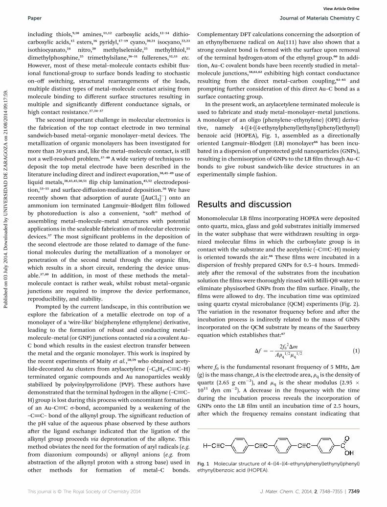
Fig. 1 Molecular structure of 4-((4-((4-ethynylphenyl)ethynyl)phenyl)ethynyl)benzoic acid (HOPEA).
Paper Journal of Materials Chemistry C
Publ
ishe
d on
03
July
201
4. D
ownl
oade
d by
UN
IVE
RSI
DA
D D
E Z
AR
AG
OZ
A o
n 21
/08/
2014
09:
17:5
9.
View Article Online
including thiols,9,10 amines,11,12 carboxylic acids,12–14 dithio-carboxylic acids,15 esters,16 pyridyl,17–19 cyano,20,21 isocyano,22,23
isothiocyanato,24 nitro,20 methylselenide,25 methylthiol,25
dimethylphosphine,25 trimethylsilane,26–31 fullerenes,32,33 etc.However, most of these metal–molecule contacts exhibit ux-ional functional-group to surface bonds leading to stochasticon–off switching, structural rearrangements of the leads,multiple distinct types of metal–molecule contact arising frommolecule binding to different surface structures resulting inmultiple and signicantly different conductance signals, orhigh contact resistance.27,34–37
The second important challenge in molecular electronics isthe fabrication of the top contact electrode in two terminalsandwich-based metal–organic monolayer–metal devices. Themetallization of organic monolayers has been investigated formore than 30 years and, like the metal–molecule contact, is stillnot a well-resolved problem.37–40 A wide variety of techniques todeposit the top metal electrode have been described in theliterature including direct and indirect evaporation,38,41–49 use ofliquid metals,38,43,45,50,51 ip chip lamination,45,52 electrodeposi-tion,53–55 and surface-diffusion-mediated deposition.56 We haverecently shown that adsorption of aurate ([AuCl4]
�) onto anammonium ion terminated Langmuir–Blodgett lm followedby photoreduction is also a convenient, “so” method ofassembling metal–molecule–metal structures with potentialapplications in the scaleable fabrication of molecular electronicdevices.57 The most signicant problems in the deposition ofthe second electrode are those related to damage of the func-tional molecules during the metallization of a monolayer orpenetration of the second metal through the organic lm,which results in a short circuit, rendering the device unus-able.37,40 In addition, in most of these methods the metal–molecule contact is rather weak, whilst robust metal–organicjunctions are required to improve the device performance,reproducibility, and stability.
Prompted by the current landscape, in this contribution weexplore the fabrication of a metallic electrode on top of amonolayer of a ‘wire-like’ bis(phenylene ethynylene) derivative,leading to the formation of robust and conducting metal–molecule–metal (or GNP) junctions contacted via a covalent Au–C bond which results in the easiest electron transfer betweenthe metal and the organic monolayer. This work is inspired bythe recent experiments of Maity et al.,58,59 who obtained acety-lide-decorated Au clusters from arylacetylene (–C6H4–C^C–H)terminated organic compounds and Au nanoparticles weaklystabilized by polyvinylpyrrolidone (PVP). These authors havedemonstrated that the terminal hydrogen in the alkyne (–C^C–H) group is lost during this process with concomitant formationof an Au–C^C s-bond, accompanied by a weakening of the–C^C– bond of the alkynyl group. The signicant reduction ofthe pH value of the aqueous phase observed by these authorsaer the ligand exchange indicated that the ligation of thealkynyl group proceeds via deprotonation of the alkyne. Thismethod obviates the need for the formation of aryl radicals (e.g.from diazonium compounds) or alkynyl anions (e.g. fromabstraction of the alkynyl proton with a strong base) used inother methods for formation of metal–C bonds.
This journal is © The Royal Society of Chemistry 2014
Complementary DFT calculations concerning the adsorption ofan ethynylbenzene radical on Au(111) have also shown that astrong covalent bond is formed with the surface upon removalof the terminal hydrogen-atom of the ethynyl group.60 In addi-tion, Au–C covalent bonds have been recently studied in metal–molecule junctions,58,61,62 exhibiting high contact conductanceresulting from the direct metal–carbon coupling,63–65 andprompting further consideration of this direct Au–C bond as asurface contacting group.
In the present work, an arylacetylene terminated molecule isused to fabricate and study metal–monolayer–metal junctions.A monolayer of an oligo (phenylene–ethynylene) (OPE) deriva-tive, namely 4-((4-((4-ethynylphenyl)ethynyl)phenyl)ethynyl)benzoic acid (HOPEA), Fig. 1, assembled as a directionallyoriented Langmuir–Blodgett (LB) monolayer66 has been incu-bated in a dispersion of unprotected gold nanoparticles (GNPs),resulting in chemisorption of GNPs to the LB lm through Au–Cbonds to give robust sandwich-like device structures in anexperimentally simple fashion.
Results and discussion
Monomolecular LB lms incorporating HOPEA were depositedonto quartz, mica, glass and gold substrates initially immersedin the water subphase that were withdrawn resulting in orga-nized molecular lms in which the carboxylate group is incontact with the substrate and the acetylenic (–C^C–H) moietyis oriented towards the air.66 These lms were incubated in adispersion of freshly prepared GNPs for 0.5–4 hours. Immedi-ately aer the removal of the substrates from the incubationsolution the lms were thoroughly rinsed withMilli-Q® water toeliminate physisorbed GNPs from the lm surface. Finally, thelms were allowed to dry. The incubation time was optimizedusing quartz crystal microbalance (QCM) experiments (Fig. 2).The variation in the resonator frequency before and aer theincubation process is indirectly related to the mass of GNPsincorporated on the QCM substrate by means of the Sauerbreyequation which establishes that:67
Df ¼ � 2f02Dm
Arq1=2mq
1=2(1)
where f0 is the fundamental resonant frequency of 5 MHz, Dm(g) is themass change, A is the electrode area, rq is the density ofquartz (2.65 g cm�3), and mq is the shear modulus (2.95 �1011 dyn cm�2). A decrease in the frequency with the timeduring the incubation process reveals the incorporation ofGNPs onto the LB lm until an incubation time of 2.5 hours,aer which the frequency remains constant indicating that
J. Mater. Chem. C, 2014, 2, 7348–7355 | 7349

Fig. 2 Amount of gold deposited onto a HOPEA monomolecular filmincubated in a dispersion of GNPs as a function of the incubation time.
Journal of Materials Chemistry C Paper
Publ
ishe
d on
03
July
201
4. D
ownl
oade
d by
UN
IVE
RSI
DA
D D
E Z
AR
AG
OZ
A o
n 21
/08/
2014
09:
17:5
9.
View Article Online
further incorporation of GNPs onto the LB lm does notoccur.
UV-vis spectra were recorded before and aer the incubationprocess in order to verify the assembly of GNPs onto the organiclayer (Fig. 3). For the purpose of comparison, the inset of Fig. 3shows the UV-vis spectrum of the aqueous dispersion of GNPs.The UV-vis spectrum of the pristine LB lm features oneabsorption band centered at 280 nm, attributable to p–p*
electronic transitions associated with the OPE backbone ofHOPEA.66 The spectrum of the LB lm aer the incubationprocess features two absorption bands at 259 nm and at ca. 540nm,68–71 revealing the incorporation of the GNPs onto the LBlm. A signicant red-shi of the surface plasmon resonance(SPR) band from 515 nm in the dispersion to 545 nm for theimmobilized GNPs on the LB lm surface is indicative of achange in the dielectric constant surrounding the nanoparticle.In addition, this shi in the maximum absorption position of
Fig. 3 UV-vis spectrum of a pristine HOPEA monomolecular LB filmand a spectrum of the same film after incubation in a dispersion ofGNPs for 2.5 hours. The inset figure shows the UV-vis spectrum of theaqueous dispersion of GNPs.
7350 | J. Mater. Chem. C, 2014, 2, 7348–7355
the SPR band is consistent with an interaction of the GNPs andthe organic lm.61
The assembly of GNPs onto the lm has also been demon-strated by XPS. Fig. 4 shows the XPS spectrum of a HOPEA LBlm on a glass substrate aer the incubation process in adispersion of GNPs. The Au4f region shows two peaks at 84.1and 87.8 eV attributable to the presence of metallic gold.72–75
However, neither QCM, UV-vis spectroscopy nor XPS resultsprovide any information about the distribution, shape, or sizeof the GNPs on the surface of the lm. To investigate theseissues, Atomic Force Microscopy (AFM) and Scanning ElectronMicroscopy (SEM) images of LB lms before and aer incuba-tion in a dispersion of GNPs were obtained (Fig. 5). The pristineHOPEA lm shows a very homogeneous surface. In contrast,aer incubation in the dispersion of GNPs both AFM and SEMimages show the appearance of spots distributed all over thelm revealing the presence of GNPs. The diameter of the GNPsimmobilized on the monolayer surface determined by SEM wasin the 15–30 nm range whilst the GNP height is in the 6–25 nmrange as determined from AFM images. These compare with the7–28 nm range of particle sizes determined for the initialdispersions by Dynamic Light Scattering (DLS) methods, seeExperimental section.
In addition, incubation of HOPEA monomolecular LB lmscaused signicant modication to the appearance, physicalcharacteristics, and composition of the lm surface. Surfacemodication is veried by differences in contact anglemeasurements from pristine and incubated lms of HOPEA in adispersion of GNPs. The contact angle of water onto a pristineHOPEA LB lm deposited onto a glass substrate is 60�, consis-tent with a well-formed hydrophobic LB lm. Aer incubationof the HOPEA monomolecular LB lm in a dispersion of GNPsfor 2.5 h the contact angle is reduced to 43� indicating a morehydrophilic surface, with a contact angle value surprisinglyclose to the value associated with a bare gold substrate (39�).
The previous set of experiments demonstrates the assemblyof GNPs onto the monomolecular lm. Nevertheless, two
Fig. 4 XPS spectrum of Au4f photoelectrons of a HOPEA mono-molecular LB film on a glass substrate after incubation in a dispersionof GNPs for 2.5 hours.
This journal is © The Royal Society of Chemistry 2014

Fig. 5 AFM (top) and SEM (bottom) images of a pristine HOPEAmonomolecular LB film (left) deposited onto a mica substrate and thesame LB film after incubation for 2.5 hours in a dispersion of GNPs(right). Images are 2� 2 mm2 in size and the Z range of the AFM imagesis 30 nm. For a better view of the size and shape of the GNPs both AFMand SEM images have been magnified (500 � 500 nm).
Fig. 6 Raman spectrum of HOPEA powder, SERS spectrum of apristine HOPEA monomolecular LB film, and SERS spectrum of aHOPEA monomolecular LB film after incubation in a dispersion ofGNPs.
Paper Journal of Materials Chemistry C
Publ
ishe
d on
03
July
201
4. D
ownl
oade
d by
UN
IVE
RSI
DA
D D
E Z
AR
AG
OZ
A o
n 21
/08/
2014
09:
17:5
9.
View Article Online
further important questions concerning the strategy proposedin this paper to fabricate the top contact electrode in metal–organic monolayer–GNP sandwich structures have still to beaddressed: (i) what is the nature of the gold–organic layerinteraction? and (ii) does the fabrication of individual GNPelectrodes induce the formation of short-circuits due to metalliccontact between the bottom and top-contact electrodes or, incontrast, do the GNPs serve as well-behaved top contactelectrodes?
As mentioned in the Introduction of this paper, it has beendemonstrated58,59,75,76 that terminal alkynes react with GNPswith simultaneous abstraction of acetylenic hydrogen to giveAu–C^C stabilized structures.51,68,69 With a view to exploringrelated processes between the terminal alkyne moiety in surfacebound HOPEA lms and the deposited GNPs vibrational spec-troscopy is a particularly useful tool, with several Raman andSERS studies61,63,65,77 having shown evidence for the formation ofa carbon–gold covalent bond in related systems. Fig. 6 showsthe Raman spectra of HOPEA in the solid state as a powder, aswell as the SERS spectrum of a HOPEA pristine LB lm depos-ited on silver mirrors and the spectrum aer the incubationprocedure in a dispersion of GNPs. All spectra show three majorvibrational bands at 2216, 1598, and 1131 cm�1. The highestwavenumber band is associated with the localized vibrationalmotion of the internal alkyne moiety; the band at 1598 cm�1 isassigned to the symmetric stretch of the three aromatic ringsalong the long axis of the molecule, and the one at 1131 cm�1
arises from symmetric C–H bending of the phenyl C–H bonds(there are 12 phenyl C–H bonds in HOPEA).78,79 This band at ca.1131 cm�1 is also present in an analogous compound to HOPEAwithout the terminal acetylene group, i.e., (4-[4-(phenylethynyl)-phenylethynyl benzoic acid).79 The spectrum of the HOPEA LBlm aer the incubation process exhibits a low intensity band at399 cm�1 indicative of the presence of a covalent Au–C
This journal is © The Royal Society of Chemistry 2014
s-bond.56 Such a band is not present in the Raman spectrum ofHOPEA powder, nor in the spectra of pristine HOPEA LB lms.In addition, the small band at 2110 cm�1, due to the terminalC^C group, in the powder Raman spectrum and the SERSspectrum of the HOPEA pristine lm is broadened and down-shied to 1990 cm�1 aer incubation of the lms in a disper-sion of GNPs, also indicative of the formation of a –C^C–Aubond.80
The electrical characteristics of the structures fabricated asdescribed above were determined from collection and analysisof current–voltage (I–V) curves arising from charge ow acrossthe organic lms. Analysis of the I–V curves not only givesinformation concerning the conductance in the metal–mono-layer–GNP assemblies but can also be used to rule out theformation of electrical short-circuits by incursion of the GNPsthrough the organic lm that eventually lead to direct metal-to-metal contacts. As described in a previous paper, I–V curveswere recorded with a conductive-AFM (Bruker ICON) in the PeakForce Tunneling AFM (PF-TUNA™) mode.57 This operationmode of the AFM is a valuable method for conductivity mappingof delicate samples since it avoids lateral forces that mayotherwise damage the tip coating and the so sample surface.This mode also facilitates the use of cantilevers with low springconstant. The peak force tunneling AFM used here combines aconducting AFM tip and associated low-noise current amplierwith a “tapping”mode AFM to probe current ow through these
J. Mater. Chem. C, 2014, 2, 7348–7355 | 7351

Journal of Materials Chemistry C Paper
Publ
ishe
d on
03
July
201
4. D
ownl
oade
d by
UN
IVE
RSI
DA
D D
E Z
AR
AG
OZ
A o
n 21
/08/
2014
09:
17:5
9.
View Article Online
metal–molecule–GNP junctions. Nevertheless a compromisehas to be reached with respect to the set-point force beforerecording the I–V curves. This compromise involves notapplying a too high peak force during the measurements, whichwould result in large deformation of the monolayer underlyingthe GNPs, or too little force which would result in inadequatecontact between the tip and the surface leading to ineffectiveelectrical probing. The deformation or damage of the mono-layer has been investigated as a function of the tip loading force(set-point force) to determine the most suitable set-point forcecompromise. Fig. 7 shows a c-AFM image of a HOPEA LB lmaer the incubation process in a GNP dispersion using a set-point force of 3.35 nN. Four gold nanoparticles labeled as GNP1,GNP2, GNP3, and GNP4 are clearly visible in this image. In theset-point force range between 3.35 and 10 nN, the sectionanalysis shows practically constant heights of 25, 19.5, 13.5, and11.5 nm for GNP1, GNP2, GNP3, and GNP4, respectively. Thepractically constant GNP height in this set-point force rangeindicates that no signicant deformation of the monolayeroccurs and that the GNPs are not substantially pushed into themonolayer by the AFM tip. If the set-point force is increased upto 16.75 nN, the section analysis of the GNPs gives heights of 21,16.2, 10 and 9 nm for GNP1, GNP2, GNP3, and GNP4 respec-tively. These reduced height values reveal deformation of themonolayer for this applied set-point force. A further increase inthe deformation of the monolayer occurs when a set-point forceof 25.2 nN is applied since the section analysis shows heights of18.8, 14.3, 8.8, and 7.4 nm for GNP1, GNP2, GNP3 and GNP4,respectively. Moreover, if the set-point force is tuned down tolow values, e.g. to 6.7 nN, the section analysis of these GNPsshows heights of 24.2, 19.1, 13 and 11.3 nm. This restoration ofheight values indicates that the deformation produced inthe monolayer aer applying a high set-point force (25.2 nN) iselastic and does not induce permanent damage of theorganic layer.
Fig. 7 Height of GNPs determined with the c-AFM at the indicatedset-point forces together with the average conductance valuesmeasured by locating the tip of the c-AFM on the indicated GNPs. Theinset top image shows a representative example of a 350 � 350 nm2
image where GNPs can be clearly distinguished and was used toposition the c-AFM tip onto the GNPs; the Z range is 50 nm.
7352 | J. Mater. Chem. C, 2014, 2, 7348–7355
Having evaluated the inuence of the applied set-point forceon the monolayer, the I–V curves were recorded. To record thesecurrent–voltage curves, the c-AFM tip was located on thenanoparticle and a bias voltage was applied between the sampleand the tip and tip voltage was swept (�1.1 V) with theLB-coated Au substrate set to ground. When a set-point force of3.35 nNwas used any resulting current whichmight have owedis below the detection limit (see conductance versus force datain Fig. 7), whilst for a set-point force between 3.35 and 10 nN theI–V curves show low conductance. These results suggest thatwhen low set-point forces are used to record the I–V curves, theelectrical contact between the tip and the GNP is not sufficientto support measureable electrical current ow. Nevertheless,when a higher set-point force (between 16.7 and 25.1 nN) wasapplied, the I–V curves show a signicant conductance (Fig. 7),revealing that for these set-point forces there is a good electricalcontact between the tip and the GNP, while no damage to themonolayer occurs. Fig. 8 shows a representative I–V curve of allthe curves (ca. 550) recorded on different GNPs when a set-pointforce of 16.7 nm was applied. The bottom inset of Fig. 8 showsthe conductance histogram built from all the experimental data(10 I–V curves on each of different GNPs) in the �0.45 to 0.45 Vohmic region for each of the 550 I–V curves obtained experi-mentally by placing the AFM tip on top of different GNPsapplying a set-point force of 16.7 nN. Different GNPs yielddifferent I–V curves whose slope (and thereby conductance ofthe device) increases with the GNP diameter. All the curvesmeasured exhibit the typical shape observed for metal–mole-cule–metal junctions, with a linear section only at relatively lowbias voltages and increasing curve gradients at higher bias.Importantly, only curves with this behavior were observed, both
Fig. 8 Representative I–V curve obtained experimentally by posi-tioning the c-AFM tip on top of a GNP when a set-point force of 16.7nN was applied. Inset bottom: conductance histogram built from allthe experimental data from �0.45 to 0.45 V for each I–V curveobtained (ca. 550 curves). Inset top: representative I–V curve obtainedby positioning the c-AFM tip on the organic monolayer not covered byGNPs when a set point-force of 6.7 nN was applied; if higher set-pointforces are applied damage on the LB film is produced.
This journal is © The Royal Society of Chemistry 2014
Paper Journal of Materials Chemistry C
Publ
ishe
d on
03
July
201
4. D
ownl
oade
d by
UN
IVE
RSI
DA
D D
E Z
AR
AG
OZ
A o
n 21
/08/
2014
09:
17:5
9.
View Article Online
over GNPs and on the organic monolayer not covered by GNPs(top inset of Fig. 8), and no low resistance traces characteristicof metallic short circuits were obtained over a wide range of set-point forces which rules out the presence of short-circuitsconrming that robust and reliable top-contacts have beenconstructed without damaging the underlying organic mono-layer lm.
Experimental
In a previous paper we reported the synthesis of HOPEA as wellas the optimum conditions needed to fabricate well-ordered,defect-free and directionally oriented LB lms of thiscompound on mica, gold and quartz substrates.66 The sameprotocols have been used in this contribution to fabricateLangmuir–Blodgett (LB) lms incorporating HOPEA. A NimaTeon trough with dimensions (720 � 100) mm2, which washoused in a constant temperature (20 � 1 �C) clean room, wasused to fabricate the lms. A Wilhelmy paper plate pressuresensor was used to measure the surface pressure (p) of themonolayers. The subphase was a pH 9 NaOH aqueous solution(Milli-Q water, resistivity 18.2 MU cm). A 1 � 10�5 M solution ofHOPEA in hexane–ethanol (2 : 1) (both solvents purchased fromAldrich and used as received; purity HPLC grade 99% and>99.5%, respectively) was spread onto the aqueous surface. Thespreading solvent was allowed to completely evaporate from thesurface of the subphase over a period of at least 20 minutesbefore compression of the monolayer commenced at a constantsweeping speed of 0.015 nm2 per molecule per min. The solidsubstrates used for the transfer were cleaned carefully asdescribed elsewhere.81,82 The monolayers were deposited by thevertical dipping method onto several substrates at a constantsurface pressure of 18 mN m�1 and a speed of 3 mm min�1.
The dispersion of GNPs was prepared by adding rapidly0.5 mL of a 1.0 � 10�3 M NaBH4 aqueous solution to 30 mL of a1.0 � 10�5 M HAuCl4 aqueous solution with vigorous stirring at2 �C using an ice-water bath. The hydrodynamic diameter ofthese GNPs was found to be in the 7–28 nm range, as deter-mined by Dynamic Light Scattering (DLS). DLS measurementswere carried out using a NanoZS ZEN3600 instrument fromMalvern. Incubation of the LB lms in the dispersion of GNPs(at 2 �C) took place immediately aer mixing the reactants.
UV-vis spectra were acquired on a Varian Cary 50 spectro-photometer and recorded using a normal incident angle withrespect to the lm plane. Atomic force microscopy (AFM)experiments to study the topography of the monolayers wereperformed by means of a Multimode 8 AFM system from Veeco,in tapping mode. The data were collected with a scan rate of1 Hz and under ambient air conditions by using a siliconcantilever provided by Bruker, with a force constant of 40 mNm�1 and operating at a resonant frequency of 300 kHz. Scan-ning electron microscopy (SEM) images were obtained with aJEOL JSM 6400 microscope. X-ray photoelectron spectroscopy(XPS) spectra were acquired on a Kratos AXIS ultra DLD spec-trometer with a monochromatic Al Ka X-ray source (1486.6 eV)using a pass energy of 20 eV. The photoelectron take off anglewas 90� with respect to the sample plane. To provide a precise
This journal is © The Royal Society of Chemistry 2014
energy calibration, the XPS binding energies were referenced tothe C1s peak at 284.6 eV. Quartz crystal microbalance (QCM)measurements were carried out using a Stanford ResearchSystem instrument and employing AT-cut, a-quartz crystals witha resonant frequency of 5 MHz having circular gold electrodespatterned on both sides. Contact angle experiments were per-formed with a commercial optical tensiometer Theta Lite fromAttension. Raman and surface-enhanced Raman scattering(SERS) spectra were collected using a Confocal Raman Imagingfrom Witec, model Alpha300M+ with an excitation wavelengthof 633 nm. Silver islands (thickness 9.1 nm) were prepared in anEdwards model 306 vacuum coater from a resistively heatedtungsten boat. The substrates were Zuzi glass microscope slidescleaned in piranha solution for 30 min (3 : 1 97% H2SO4 : 30%H2O2), rinsed with deionized water, and dried in a stream of N2.Care: piranha solutions are exceptionally corrosive and highlyoxidizing. Contact between piranha solutions and organicmaterials is considered extremely hazardous and must be avoided.During lm deposition, the background pressure was main-tained at 5 � 10�7 Torr, and the deposition rate (0.02 nm3 s�1)was monitored on an Electron Beam Evaporator Auto 500 fromBOC Edwards. Aer deposition, annealing was performed at200 �C for 60 minutes. The conducting-AFM (c-AFM) measure-ments were performed with a Bruker ICON microscope underhumidity control, ca. 30%, with a N2 ow, in the Peak ForceTunneling AFM (PF-TUNA™) mode, and employing aPF-TUNA™ cantilever from Bruker (coated with Pt/Ir 20 nm, ca.25 nm radius, 0.4 N m�1 spring constant and 70 kHz resonancefrequency).
Conclusions
In this contribution, GNPs have been assembled onto anorganic LB lm to give arrays of metal–molecule–GNP devices.Formation of covalent Au–C s-bonds through a simple wet-chemical procedure has been demonstrated by SERS whilst I–Vcurves ruled out the presence of short-circuits. The terminalalkyne moiety therefore appears to be a suitable functionalgroup for the subsequent deposition of metal nanoparticleswhich can serve as the top contact electrode. The electricalmeasurements averaged over multiple gold–molecule–GNPassemblies show the suitability of this approach of formingC–Au bonds to the top GNP contact. This could be a usefulapproach for future nano-electronic assemblies which exploitmore robust C–Au junctions rather than the typically moreuxional chemisorption chemical bonds used in conventionalself-assembly. If needed these GNPs could be employed as seedsfor deposition of a contiguous metal lm using complementarymethods such as electroless metal deposition subsequentlyleading to a controlled preparation of the top contact electrodein metal–monolayer–metal devices with a signicant inhibitionin the formation of short-circuits.
Acknowledgements
P.C., I.G., F.P.-M., and S.M. are grateful for nancial assistancefrom Ministerio de Economıa y Competitividad from Spain and
J. Mater. Chem. C, 2014, 2, 7348–7355 | 7353

Journal of Materials Chemistry C Paper
Publ
ishe
d on
03
July
201
4. D
ownl
oade
d by
UN
IVE
RSI
DA
D D
E Z
AR
AG
OZ
A o
n 21
/08/
2014
09:
17:5
9.
View Article Online
fondos FEDER in the framework of projects CTQ2012-33198,CSIC10-4E-805, and CSD2010-00024. P.C., F.P.-M. and S.M. arealso grateful to the European SUDOE TRAIN2 project and theNanolito network through theMAT2011-13099-E project fundedby the Ministry of Economy of Spain for supporting thiscollaborative work. P.C., I.G. and S.M. acknowledge supportfrom DGA and Fondos FEDER for funding Platon researchgroup. H.M.O. and S.M. also thank their JIUZ-2013-CIE-05grant. R.J.N., P.J.L. and S.M.-G. thank EPSRC for funding, andP.J.L. also gratefully acknowledges support from the AustralianResearch Council and the award of a Future Fellowship[FT120100073]. H.M.O. is grateful for nancial assistance fromSecretarıa Nacional de Educacion Superior, Ciencia, Tecnologıae Innovacion from Ministerio de Educacion (Ecuador). Theauthors also thank I. Echaniz, G. Antorrena, I. Rivas, R. Valero,and C. Cuesta for technical support.
Notes and references
1 D. Xiang, H. Jeong, T. Lee and D. Mayer, Adv. Mater., 2013,25, 4845–4867.
2 M. Tsutsui and M. Taniguchi, Sensors, 2012, 12, 7259–7298.3 B. Branchi, F. Simeone and M. Rampi, Top. Curr. Chem.,2012, 313, 85–119.
4 C. C. Jia and X. F. Guo, Chem. Soc. Rev., 2013, 42, 5642–5660.5 M. Kiguchi and K. Satoshi, ChemPhysChem, 2012, 13, 1116–1126.
6 M. Ratner, Nat. Nanotechnol., 2013, 8, 378–381.7 Editorial, Nat. Nanotechnol., 2013, 8, 385–389.8 Editorial, Nat. Nanotechnol., 2013, 8, 377.9 L. J. Richter, C. S.-C. Yang, P. T. Wilson, C. A. Hacker,R. D. van Zee, J. J. Stapleton, D. L. Allara, Y. Yao andJ. M. Tour, J. Phys. Chem. B, 2004, 108, 12547–12559.
10 H. Hakkinen, Nat. Chem., 2012, 4, 443–455.11 M. S. Hybertsen, L. Venkataraman, J. E. Klare, A. Cwhalley,
M. L. Steigerwald and C. Nuckolls, J. Phys.: Condens.Matter, 2008, 20, 374115.
12 A. Villares, D. P. Lydon, P. J. Low, B. J. Robinson,G. J. Ashwell, F. M. Royo and P. Cea, Chem. Mater., 2008,20, 258–264.
13 S. Martin, W. Haiss, S. Higgins, P. Cea, M. C. Lopez andR. J. Nichols, J. Phys. Chem. C, 2008, 112, 3941–3948.
14 L. M. Ballesteros, S. Martın, J. Cortes, S. Marques-Gonzalez,S. J. Higgins, R. J. Nichols, P. L. Low and P. Cea, Chem.–Eur.J., 2013, 19, 5352–5363.
15 Y. Xing, T. H. Park, R. Venkatramani, S. Reinan,D. N. Beratan, M. J. Therien and E. Borguet, J. Am. Chem.Soc., 2010, 132, 7946–7956.
16 A. Villares, D. P. Lydon, B. J. Robinson, G. Ashwell,F. M. Royo, P. J. Low and P. Cea, Surf. Sci., 2008, 602,3683–3687.
17 B. Q. Xu and N. J. Tao, Science, 2003, 301, 1221–1223.18 S. Y. Quek, M. Kamenetska, M. L. Stigerwald, H. J. Choi,
S. G. Louie, M. S. Hybertsen, J. B. Neaton andL. Venkataraman, Nat. Nanotechnol., 2009, 4, 230–234.
7354 | J. Mater. Chem. C, 2014, 2, 7348–7355
19 W. Hong, D. Z. Manrique, P. Moreno-Garcıa, M. Gulcur,A. Mishchenko, C. J. Lambert, M. R. Bryce andT. Wandlowski, J. Am. Chem. Soc., 2012, 134, 2292–2304.
20 L. A. Zotti, T. Kirchner, J. C. Cuevas, F. Pauli, T. Huhn,E. Scheer and A. Erbe, Small, 2010, 6, 1929–1535.
21 A. Mishchenko, L. A. Zotti, D. Vonlanthen, M. Burkle,F. Pauly, J. C. Cuevas, M. Mayor and T. Wandlowski, J. Am.Chem. Soc., 2011, 133, 184–187.
22 L. Venkataraman, J. E. Klare, I. W. Tam, C. Nuckolls,M. S. Hybertsen and M. N. Steigerwald, Nano Lett., 2006, 6,458–462.
23 B. Kim, J. M. Beebe, Y. Jun, X. Y. Zhu and C. D. Frisbie, J. Am.Chem. Soc., 2006, 128, 4970–4971.
24 C. H. Ko, M. J. Huang, M. D. Fu and C. H. Chen, J. Am. Chem.Soc., 2010, 132, 756–764.
25 Y. S. Park, A. C. Whalley, M. Kamenetska, M. L. Steigerwald,M. S. Hybertsen, C. Nuckolls and L. Venkataraman, J. Am.Chem. Soc., 2007, 15768–15769.
26 G. Pera, S. Martin, L. M. Ballesteros, A. J. Hope, P. J. Low,R. J. Nichols and P. Cea, Chem.–Eur. J., 2010, 16, 13398–13405.
27 S. Marques-Gonzalez, D. S. Yut, J. A. K. Howard, S. Martın,H. M. Osorio, V. M. Garcıa-Suarez, R. J. Nichols, S. J. Higgins,P. Cea and P. J. Low, Dalton Trans., 2013, 42, 338–341.
28 N. Katsonis, A. Marchenko, S. Taillemite, D. Fichou,G. Chouraqui, C. Aubert and M. Malacria, Chem.–Eur. J.,2003, 9, 2574–2581.
29 N. Katsonis, A. Marchenko, D. Fichou and N. Barret, Surf.Sci., 2008, 602, 9–16.
30 A. Nion, N. Katsonis, A. Marchenko, C. Aubert and D. Fichou,New J. Chem., 2013, 37, 2261–2265.
31 E. G. Petrov, A. Marchenko, O. Kapitanchuk, N. Katsonis andD. Fichou, Mol. Cryst. Liq. Cryst., 2014, 589, 3–20.
32 C. A. Martin, D. Ding, J. K. Sorensen, T. Bjornholm, J. M. vanRuitenbeek and H. S. J. van der Zant, J. Am. Chem. Soc., 2008,130, 13198–13199.
33 J. Fock, J. K. Sorensen, E. Loertscher, T. Vosch, C. A. Martin,H. Riel, K. Kilsa, T. Bjornholm and H. S. J. van der Zant, Phys.Chem. Chem. Phys., 2011, 13, 2236–2241.
34 G. K. Ramachandran, T. J. Hopson, A. M. Rawlett,L. A. Nagahara, A. Primak and S. M. Lindsay, Science, 2003,300, 1413–1416.
35 Z. K. Keane, J. W. Ciszek, J. M. Tour and D. Natelson, NanoLett., 2006, 6, 1518–1521.
36 S. Yasuda, S. Yoshida, J. Sasaki, Y. Okutsu, T. Nakamura,A. Taninaka, O. Takeuchi and H. Shigekawa, J. Am. Chem.Soc., 2006, 128, 7746–7747.
37 D. Vuillaume, Proc. IEEE, 2010, 1–12.38 H. Haick and D. Cahen, Acc. Chem. Res., 2008, 41, 359–366.39 H. B. Akkerman and B. De Boer, J. Phys.: Condens. Matter,
2008, 20, 013001.40 D. Vuillaume, C. R. Phys., 2008, 9, 78–94.41 L. Costelle, M. T. Raisanen, J. T. Joyce, C. Silien,
L.-S. Johansson, J. M. Campbell and J. Raisanen, J. Phys.Chem. C, 2012, 116, 22602–22607.
This journal is © The Royal Society of Chemistry 2014

Paper Journal of Materials Chemistry C
Publ
ishe
d on
03
July
201
4. D
ownl
oade
d by
UN
IVE
RSI
DA
D D
E Z
AR
AG
OZ
A o
n 21
/08/
2014
09:
17:5
9.
View Article Online
42 R. Lovrincic, O. Kraynis, R. Har-Lavan, A.-E. Haj-Yahya,W. Li, A. Vilan and D. Cahen, J. Phys. Chem. Lett., 2013, 4,426–430.
43 R. L. McCreery and A. J. Bergren, Adv. Mater., 2009, 21, 4303–4322.
44 R. M. Metzger, T. Xu and I. R. Peterson, J. Phys. Chem. B,2001, 105, 7280–7290.
45 R. T. W. Popoff, K. L. Kavanagh and H.-Z. Yu, Nanoscale,2011, 3, 1434–1445.
46 A. Scott, D. B. Janes, C. Risko and M. A. Ratner, Appl. Phys.Lett., 2007, 91, 033508.
47 Z. Shi, P. Lu and A. V. Walker, Langmuir, 2012, 28, 16909–16916.
48 A. V. Walker, T. B. Tighe, O. M. Cabarcos, M. D. Reinard,B. C. Haynie, S. Uppili, N. Winograd and D. L. Allara, J.Am. Chem. Soc., 2004, 126, 3954–3963.
49 Z. Zhu, D. L. Allara and N. Winograd, Appl. Surf. Sci., 2006,252, 6686–6688.
50 R. Har-Lavan, O. Yaffe, P. Joshi, R. Kazaz, H. Cohen andD. Cahen, AIP Adv., 2012, 2, 012164–012213.
51 O. Yaffe, L. Scheres, L. Segev, A. Biller, I. Ron, E. Salomon,M. Giesbers, A. Kahn, L. Kronik, H. Zuilhof, A. Vilan andD. Cahen, J. Phys. Chem. C, 2010, 114, 10270–10279.
52 S. Pookpanratana, J. W. F. Robertson, C. Jaye, D. A. Fischer,C. A. Richter and C. A. Hacker, Langmuir, 2013, 29, 2083–2091.
53 Y.-D. Chiu, W.-P. Dow, K. Krug, Y.-F. Liu, Y.-L. Lee andS.-L. Yau, Langmuir, 2012, 28, 14476–14487.
54 C. Silien and M. Buck, J. Phys. Chem. C, 2008, 112, 3881–3890.
55 C. Silien, D. E. Lahaye, M. Caffio, R. Schaub,N. R. Champness and M. Buck, Langmuir, 2011, 27, 2567–2574.
56 A. P. Bonifas and R. L. McCreery, Nat. Nanotechnol., 2010, 5,612–617.
57 S. Martin, G. Pera, L. M. Ballesteros, A. J. Hope, S. Marques-Gonzalez, P. J. Low, F. Perez-Murano, R. J. Nichols andP. Cea, Chem.–Eur. J., 2014, 20, 3421–3426.
58 P. Maity, H. Tsunoyama, M. Yamauchi, S. Xie andT. Tsukuda, J. Am. Chem. Soc., 2011, 133, 20123–20125.
59 P. Maity, S. Takano, S. Yamazoe, T. Wakabayashi andT. Tsukuda, J. Am. Chem. Soc., 2013, 135, 9450–9457.
60 M. J. Ford, R. C. Ho and A. McDonagh, J. Phys. Chem. B,2005, 109, 20387–20392.
61 L. Laurentius, S. R. Stoyanov, S. Gusarov, A. Kovalenko,R. Du, G. P. Lopinski and M. T. McDermott, ACS Nano,2011, 5, 4219–4227.
62 D. M. Shewchuk and M. T. McDermott, Langmuir, 2009, 25,4556–4563.
This journal is © The Royal Society of Chemistry 2014
63 Z. L. Cheng, R. Skouta, H. Vazquez, J. R. Widawsky,S. Schneebeli, W. Chen, M. S. Hybertsen, R. Breslow andL. Venkataraman, Nat. Nanotechnol., 2011, 6, 353–357.
64 T. Hines, I. Dıez-Perez, H. Nakamura, T. Shimazaki, Y. Asaiand N. Tao, J. Am. Chem. Soc., 2013, 135, 3319–3322.
65 W. Hong, H. Li, S.-X. Liu, Y. Fu, J. Li, V. Kaliginedi,S. Decurtins and T. Wandlowski, J. Am. Chem. Soc., 2012,134, 19425–19431.
66 L. M. Ballesteros, S. Martın, C. Momblona, S. Marques-Gonzalez, M. C. Lopez, R. J. Nichols, P. J. Low and P. Cea,J. Phys. Chem. C, 2012, 116, 9142–9150.
67 G. Sauerbrey, Z. Phys., 1959, 155, 206–222.68 V. Amendola and M. Meneghetti, J. Phys. Chem. C, 2009, 113,
4277–4285.69 W. Haiss, N. T. K. Thanh, J. Aveyard and D. G. Fernig, Anal.
Chem., 2007, 79, 4215–4221.70 H. Itoh, K. Naka and Y. Chujo, J. Am. Chem. Soc., 2004, 126,
3026–3027.71 M. Treguer-Delapierre, J. Majimel, S. Mornet, E. Duguet and
S. Ravaine, Gold Bull., 2008, 41, 195–207.72 H.-G. Boyen, G. Kastle, F. Weigl, B. Koslowski, C. Dietrich,
P. Ziemann, J. P. Spatz, S. Riethmuller, C. Hartmann,M. Moller, G. Schmid, M. G. Garnier and P. Oelhafen,Science, 2002, 297, 1533–1536.
73 M. M. Kemp, A. Kumar, S. Mousa, T.-J. Park, P. Ajayan,N. Kubotera, S. A. Mousa and R. J. Linhardt,Biomacromolecules, 2009, 10, 589–595.
74 G. Liu, E. Luais and J. J. Gooding, Langmuir, 2011, 27, 4176–4183.
75 C. Shan, H. Yang, D. Han, Q. Zhang, A. Ivaska and L. Niu,Biosens. Bioelectron., 2010, 25, 1070–1074.
76 R. Casado, M. Contel, M. Laguna, P. Romero and S. Sanz, J.Am. Chem. Soc., 2003, 125, 11925–11935.
77 Z. L. Cheng, R. Skouta, H. Vazquez, J. R. Widawsky,S. Schneebeli, W. Chen, M. S. Hybertsen, R. Breslow andL. Venkataraman, Nat. Nanotechnol., 2011, 6, 353–357.
78 A. Beeby, K. S. Findlay, P. J. Low, T. B. Marder, P. Matousek,A. W. Parker, S. R. Rutter and M. Towrie, Chem. Commun.,2003, 2406–2407.
79 A. Villares, G. Pera, S. Martin, R. J. Nichols, D. P. Lydon,L. Applegarth, A. Beeby, P. J. Low and P. Cea, Chem. Mater.,2010, 22, 2041–2049.
80 W. Hong, H. Li, S.-X. Liu, Y. Fu, J. Li, V. Kaliginedi,S. Decurtins and T. Wandlowski, J. Am. Chem. Soc., 2012,47, 19425–19431.
81 P. Cea, J. P. Morand, J. S. Urieta, M. C. Lopez and F. M. Royo,Langmuir, 1996, 12, 1541–1544.
82 S. Martın, P. Cea, C. Lafuente, F. M. Royo and M. A. C. Lopez,Surf. Sci., 2004, 563, 27–40.
J. Mater. Chem. C, 2014, 2, 7348–7355 | 7355
Copyright © 2022 FDOKUMEN


![A vacuum ultraviolet laser photoionization and pulsed field ionization study of nascent S([sup 3]P[sub 2,1,0]) and S([sup 1]D[sub 2]) formed in the 193.3 nm photodissociation of CS[sub](https://static.fdokumen.com/doc/165x107/633369ba9d8fc1106803cb07/a-vacuum-ultraviolet-laser-photoionization-and-pulsed-field-ionization-study-of.jpg)