Electrochemical kinetics of hydrogen intercalation in gadolinium switchable mirrors
Upload
independentCategory
view
1download
0
Journal of The Electrochemical Society, 154 �10� G207-G214 �2007� G207
Electrical Properties of Atomic-Layer-Deposited ThinGadolinium Oxide High-k Gate DielectricsS. Dueñas,a,z H. Castán,a H. García,a A. Gómez,a L. Bailón,a K. Kukli,b,c
T. Hatanpää,c J. Lu,d M. Ritala,c,* and M. Leskeläc
aDepartamento de Electricidad y Electrónica, E.T.S.I. Telecomunicación, Universidad de Valladolid,47011 Valladolid, SpainbInstitute of Experimental Physics and Technology, University of Tartu, 51010 Tartu, EstoniacDepartment of Chemistry, University of Helsinki, FIN-00014 Helsinki, FinlanddÅngström Microstructure Laboratory, Department of Engineering Sciences, Uppsala University,SE 75121 Uppsala, Sweden
Amorphous or cubic Gd2O3 thin films were grown from tris�2,3-dimethyl-2-butoxy�gadolinium�III�, Gd�OC�CH3�2CH�CH3�2�3,and H2O precursors at 350°C. As-deposited Gd2O3 films grown on etched �H-terminated� Si�100� exhibited better leakagecurrent-voltage characteristics as well as lower flatband voltage shift than films grown on SiO2/Si substrates. Interface trapdensities were lower in Al/Gd2O3/hydrofluoric acid �HF�-etched Si samples annealed at rather high temperatures.© 2007 The Electrochemical Society. �DOI: 10.1149/1.2761845� All rights reserved.
Manuscript submitted February 20, 2007; revised manuscript received May 25, 2007. Available electronically August 2, 2007.
0013-4651/2007/154�10�/G207/8/$20.00 © The Electrochemical Society
The progressive scaling of integrated-circuit technologies stimu-lates intense study on very thin dielectric layers on semiconductors,in order to increase the functionality of microelectronic devices.However, in conventional SiO2-based technologies, as the effectivegate-oxide thickness scales toward 1 nm there is excessive leakagecurrent due to direct tunnelling. On account of this limitation, SiO2must be replaced with a suitable high-dielectric-constant �k� mate-rial, the higher k allowing a thicker gate dielectric that reduces tun-nelling while maintaining the electric fields necessary for controllingthe channel current. In the search for proper candidates of alterna-tive dielectrics, the rare-earth �RE� oxides are attractive based onenergy considerations, i.e., RE metals are much more reactive withoxygen than other transition metals1 and have a high conductionband offset.2 RE oxides have received considerable attention as al-ternative gate-oxide materials.3,4 In particular, gadolinium oxideGd2O3 is an attractive material among the RE oxides because cubicGd2O3 has one of the closest lattice matches to silicon. Thin films ofGd2O3 have been proposed for gate-dielectric applications5,6 be-cause of its dielectric constant �near 16� as well as its large bandgap�5.3 eV�, thermodynamical stability, and chemical stability in con-tact with silicon.
For gate-oxide applications in the complementary metal-oxide-semiconductor �CMOS� devices for the sub-100 nm generation ofsilicon technology, the dielectrics should form high-quality inter-faces with Si with low interfacial state density, Dit, and little inter-facial roughness. Studies related to GaAs-based devices havedemonstrated7,8 that Gd2O3 epitaxial thin films grown by ultrahighvacuum vapor deposition forms an excellent insulating barrier withlow Dit, and that leads to GaAs-based MOS field-effect transistor�MOSFET� devices. In recent years, studies on electrical propertiesof Gd2O3 thin films on silicon have gained increasing interest.9-13
Before Gd2O3 can be considered as a viable dielectric material forfuture electronic devices, much more work must be done in order tounderstand the leakage conduction mechanisms as well as to controlthe interfacial structure.
Thin films of gadolinium oxide have been synthesized using sev-eral techniques such as electron-beam evaporation �EBE�,5,6,12
chemical vapor deposition �CVD�,14 low-pressure metallorganicchemical vapor deposition �LP-MOCVD�,10 reactive radio fre-quency �rf� sputtering,11 molecular beam epitaxy �MBE�,15 andatomic layer deposition �ALD�.14,16
* Electrochemical Society Active Member.z E-mail: [email protected]
In this paper, electrical characterization results of gadoliniumoxide films atomic-layer-deposited on n-type silicon from a novelprecursor are presented. The techniques used were current-voltage�I-V�, capacitance-voltage �C-V�, deep-level transient spectroscopy�DLTS�, conductance transients �G-t�, and constant-capacitance flat-band voltage transients �VFB-t�.
Experimental
Gadolinium oxide films were grown in a hot-wall horizontalflow-type ALD reactor F12017 at 350°C from tris�2,3-dimethyl-2-butoxy�gadolinium�III�, Gd�OC�CH3�2CH�CH3�2�3, and H2O. Thegadolinium precursor was evaporated at 195°C. The cycle timeswere 0.5 s for all pulses and purge periods. The films were grown todifferent thicknesses by applying 50, 100, 150, or 250 growthcycles. Some samples were directly deposited on hydrofluoric acid�HF�-etched �100� oriented n-silicon �14 � cm�, and others werefabricated on RCA-cleaned Si with chemically grown 0.9–1.2 nmthick SiO2 film. Some samples were annealed after deposition andbefore metallization in oxygen �99.999%� atmosphere at 750°C,1 atm, for 5 min.
The thicknesses of the films were evaluated from X-ray reflec-tion patterns measured with a Bruker D8 Advance X-ray diffracto-meter. The film structure was determined by the same diffractometerin grazing incidence mode �incidence angle 1°�. Film compositionwas determined by time-of-flight elastic recoil detection analysis�TOF-ERDA� on reference films of higher thickness ��50 nm�, us-ing either 53 MeV 127I10+ �measured in Helsinki, Finland� or16 MeV 35Cl7+ or 16 MeV 63Cu7+ �measured in Leuven, Belgium�projectile ion beams. Transmission electron microscopy �TEM� wasapplied for imaging the cross section of four representative sampleswith gadolinium oxide as-deposited and in annealed states. Thehigh-resolution TEM images were obtained using a field-emissiongun Technai F30 ST operating at 300 kV.
The electrical measurements were carried out onAl/Gd2O3/n-Si/Al and Al/Gd2O3/SiO2/n-Si/Al capacitors. Alumi-num dot electrodes with an area of 0.204 mm2 were E-beam evapo-rated on top of the dielectric layers through a shadow mask. To formnearly ohmic contacts to silicon substrates, the back sides of thewafers were etched in HF and metallized by evaporating a 100 nmthick Al layer.
In order to record the electrical parameters at several tempera-tures varying between 77 K and room temperature, samples werefirst cooled in darkness from room temperature to 77 K at 0 bias inan Oxford DM1710 cryostat. An Oxford ITC 502 controller wasused to monitor the temperature during the measurements. The I-Vcurves were measured with a Keithley 6517A programmable elec-trometer in the stair sweep voltage mode while the voltage step used

G208 Journal of The Electrochemical Society, 154 �10� G207-G214 �2007�G208
was 5 mV. The C-V measurements were carried out with the assis-tance of a Boonton 72B capacitance meter and a Keithley 617 pro-grammable electrometer. The capacimeter makes measurements ofshunt capacitance by applying a 1 MHz and 15 mV-level ac signaltest. Voltage bias consists of 50 mV steps. The capacitance measure-ments are made 10 s after the bias-voltage step is applied in order toprevent transient instabilities in the capacitance values.
Interfacial state densities were obtained by saturating pulseDLTS between 77 and 300 K.18,19 The bias voltage was chosen foreach sample so that the capacitor was just at the limit betweendepletion and weak inversion. A 10 ms wide pulse high enough todrive the capacitors into accumulation was applied in order to fill allinterface traps. Information on the traps was obtained by analyzingthe capacitance transient that results as the traps empty, i.e., return toequilibrium. This technique is adequate to separate the fast contri-butions of interface states from the slow ones corresponding to de-fects in the dielectric bulk, because DLTS is time sensitive andallows one to distinguish contributions with different time constants.The interface trap distribution Dit corresponding to the upper half ofthe forbidden gap �EC to midgap� was deduced from DLTS measure-ments by means of the expressions reported elsewhere.19 Low-temperature transients provide information about interface states lo-cated near the conduction bandedge, whereas high-temperaturetransients correspond to the emission of those located very near themidgap. For DLTS measurements we used a 1 MHz Boonton 72Bcapacitance meter and a HP54501 digital oscilloscope to record thecomplete capacitance transients. A Keithley 617 programmable elec-trometer was used together with a HP214B pulse generator to intro-duce the quiescent bias and the filling pulse, respectively.
DLTS technique provides the energetic distribution of interfacialstates. However, according to the disorder-induce gap states �DIGS�model proposed by He et al.,20 interface states are distributed notonly in energy but also in space. In the spatial dimension, the re-gions of distorted local bonds extend on both sides of the interface,resulting in disordered regions in the semiconductor and in the in-sulator. The spatial extension of the disordered semiconductor re-gion is very narrow, typically one or several monolayers, whereasthat of the disordered insulator region reaches several tens of ang-stroms. The shape of the DIGS distribution is exponentially decay-ing away from the interface into the insulator.21 As from DLTSmeasurements the interface width cannot be derived, and in order toget a more complete electrical characterization, it becomes suitableto carry out conductance transient measurements.22 From these con-ductance transients it is possible to obtain the DIGS state density asa function of the spatial distance to the interface and of the energyposition.23 The experimental setup of the conductance transient tech-nique consists of an HP 33120A arbitrary wave-form generator toapply the bias pulses, an EG&G 5206 two-phase lock-in analyzer tomeasure the conductance, and an HP 54501A digital oscilloscope torecord the complete conductance transient.
Finally, flatband voltage transients at temperatures between 77and 300 K have been measured by recording the gate voltage whilekeeping the capacitance constant at the initial flatband condition.24
Samples were kept under no external stress conditions: zero electricfield in the substrate, darkness conditions and no external chargeinjection. Under these conditions, the only mechanism for defecttrapping or detrapping is thermal activation by means of phonons.So, this kind of measurement allows us to obtain the energy ofsoft-optical phonons in the insulator. To obtain the flatband voltagetransients, a feedback system that varies the applied gate voltageaccordingly to keep the capacitance at its flatband voltage value hasbeen implemented. A Keithley 6517A working as programmablebias source and a 1 MHz Boonton 72B capacitance meter wereused.
Results and Discussion
Structure and composition of the films.— TOF-ERDA measure-ments were carried out on a 65 nm thick Gd2O3 film for the sake ofconvenience. The film was grown at 350°C using 2500 deposition
cycles �growth rate 0.026 nm/cycle�. The composition profiling re-vealed that the films contained 37 ± 2 atom % gadolinium and51 ± 2 atom % oxygen. Thus, the O-to-Gd ratio was close to 1.4 andthe films could be considered as oxygen deficient. In addition, thepresence of residual hydrogen and carbon was detected. The con-tents of H and C were 1.0 ± 0.5 and 0.6 ± 0.3 atom %, respectively.
TEM studies �Fig. 1� revealed the formation of continuous oxidefilms without particular grain growth. The interfacial layer wasclearly visible, and in the case of SiO2/Si substrate the thickness ofSiO2 was retained. The interfacial SiO2 layer thickness did not in-crease noticeably upon annealing. At the same time, in the case offilms grown onto HF-etched silicon, the interfacial layer thicknessincreased during annealing, although the exact composition of theinterface layers remained open. Crystal growth was not noticeablypromoted by the annealing procedure.
The Gd2O3 films tended to crystallize in quite early stages of thegrowth at 350°C �Fig. 2�. The critical crystallization thickness ap-peared to be around 10 nm. In the films with thickness higher than10 nm, cubic Gd2O3 was formed. Reflections from other phases
Figure 1. TEM images of Gd2O3 films with nominal thickness 2.2 nm onHF-etched Si in as-deposited �upper left panel� and annealed �upper rightpanel� states, and films with thickness 8.1 nm on SiO2/Si in as-deposited�lower left panel� and annealed �lower right panel� states.
Figure 2. Gd2O3 film structures represented by XRD patterns taken from thefilms with different thicknesses and on HF-etched �Si–H� or SiO2-covered Si�SiO2/Si� substrates indicated by labels. The upmost pattern represents areference well-crystallized film with relatively higher thickness.

thick
G209Journal of The Electrochemical Society, 154 �10� G207-G214 �2007� G209
were not detected in the samples of this series. Annealing at 750°Cin O2 under 1 atm pressure for 5 min did not noticeably change thefilm structure �Fig. 2�.
Electrical measurements.— Figure 3 shows current measure-ment results at several temperatures between 77 and 300 K. As theelectron encountered different barriers for gate injection and sub-strate injection, I-V plots were markedly asymmetrical. The leakagecurrent was higher at positive bias than at negative bias, because thecharge conduction was controlled by the metal/oxide interface in-stead of by the silicon/oxide interface.25 Also, a saturation of thecurrent in inversion �negative bias� was produced due to the ex-hausting of the minority carriers injected from the substrate.26 So,we only present here the results obtained under positive bias as thebest indicator of film quality, as it has been done by severalauthors.27,28
As-deposited Al/Gd2O3/HF-etched-n-Si, 750°C annealedAl/Gd2O3/HF-etched-n-Si, and as-deposited Al/Gd2O3/SiO2/n-Sisamples, all of them containing 2.2 nm thick Gd2O3, arecompared in Fig. 3a. Effective voltage �VG-VFB� values instead ofVG values are displayed to take into account the different C-V be-havior of each sample. It seems clear that the as-depositedAl/Gd O /HF-etched-n-Si sample exhibits the best I-V characteris-
Figure 3. �a� Current �I� against effective voltage �VG-VFB� curves measureMIS devices with 2.2 nm thick Gd2O3, �b� effective voltage �VG-VFB� valuedifferent samples described by labels, �c� temperature dependence of thecorresponding to the Al/Gd2O3/SiO2/n-Si sample with as-deposited 8.5 nm
2 3
tics, with an effective conduction onset of about 2.70 V at 77 K.This onset decreases as temperature increases, reaching 2.35 V atroom temperature. The annealed sample displays much poorer char-acteristics, the effective conduction onset being 1.50 V at 77 K and1.45 V at room temperature. The unannealed sample in whichGd2O3 has been deposited onto oxidized silicon has an intermediatebehavior. Also, the conduction threshold voltage is higher at 300 Kthan at 77 K. Moreover, conduction onset initially decreases from77 to 235 K, as expected, but from 250 K this onset progressivelyincreases. This means that there exists some temperature-activatedmechanism, probably related to the SiO2 film, which progressivelyblocks the current through these thin films above 250 K. This effectwas not observed either in thicker samples or in 2.2 nm thick oxidefilms deposited on HF-etched substrates. One tentative explanationfor the differences in the conduction onset and behavior of the thin-nest dielectric stack of silicon oxide is the existence of thermallyactivated defects inside the dielectric. These defects are activated attemperatures higher than 250 K and remain negatively charged. Thisnegative charge induces an extra positive charge in the substrateand/or interface layer, diminishing the local electric field in the re-gion close to the interface and giving place to a flatband voltageshift toward more positive values, V , and lower currents. A direct
veral temperatures between 77 and 300 K corresponding to Al/Gd2O3/n-Siresponding to 2.5 mA/cm2 current density as a function of temperature fort measured at constant voltage, and �d� current-electric field dependencyGd2O3 film.
d at ses corcurren
FB

depos
G210 Journal of The Electrochemical Society, 154 �10� G207-G214 �2007�G210
consequence is the displacement of the conduction onset to highereffective gate voltages.
In Fig. 3b the effective voltage values corresponding to2.5 mA/cm2 current density are displayed for several samples. Forall the cases, the effective voltage value monotonically decreases astemperature increases. Only the Al/Gd2O3/SiO2/n-Si sample with2.2 nm thick as-deposited Gd2O3 shows a different behavior fortemperatures higher than 250 K, due to the anomalous behaviormentioned above. Effective voltage values are clearly higher forannealed than for as-grown samples in the cases of films depositedon SiO2/Si substrates, whereas the opposite trend is observed forfilms deposited on HF-etched Si. The effective voltage values of theas-deposited samples fabricated on oxidized silicon clearly increasewith the film thickness, in good agreement with the dependence ofleakage current and breakdown voltage with the GdScO3 film thick-ness reported by Zhao et al.29
Figure 3c shows the current-temperature dependence for theAl/Gd2O3/SiO2/n-Si sample with 8.5 nm thick as-deposited Gd2O3.In the 200–300 K temperature range the relationship between ln�I�and 1000/T is clearly linear. Such as Arrhenius plot indicates a con-duction mechanism controlled by Poole–Frenkel �PF� emission. It isknown that for the Schottky emission mechanism an Arrhenius plotof ln�I/T2� against 1000/T is obtained. Schottky emission is con-trolled by the quality of the metal-insulator interface, while the PFmechanism is bulk-limited and relies on the traps in the insulator.The PF is associated with the field-enhanced thermal excitation ofcharge carriers from traps. As it is shown in the inset, the slopes ofthe lines do not vary appreciably with the applied voltage, indicatingthat the conduction takes place through an activated process havinga single activation energy, �E�, which follows the relation30
I = I0 exp�−�E�
KT� �1�
The activation energy values corresponding to several samplesare listed in Table I. Irrespective of the substrate treatment and thefilm thickness, the activation energy values obtained for the an-nealed samples correspond to the previously reported soft-opticalphonon energy �in the 55 ± 10 meV range�, obtained from flatbandtransient measurements.24 However, activation energy values of as-deposited samples scatter between 24 and 314 meV, indicating thatother different mechanisms take place as well, and so the combina-tion of all of them is detected.
Figure 3d shows the plot of I/E �in logarithmic scale� againstE1/2 at several temperatures, corresponding to theAl/Gd2O3/SiO2/n-Si sample with 8.5 nm thick as-deposited Gd2O3.As it is shown in the inset, there is a linear dependence in thehigh-field range, as required by the PF equation
I = I0 exp��PFE1/2
KT�E �2�
The obtained value of �PF in the 0.6–1.5 MV/cm electric fieldrange is 2.71 � 10−5 eV m1/2 V−1/2. The current in the lower elec-tric field region is probably due to tunneling of electrons from the
Table I. Activation energy values and PF coefficients obtained fromatomic-layer-deposited Gd2O3 thin films. Oxide thickness and annea
MOS Structure
Gd2O3Thickness
�nm� A
Al/Gd2O3/HF-etch-n-Si 2.2 AsAl/Gd2O3/SiO2/n-Si 2.2 AsAl/Gd2O3/HF-etch-n-Si 2.2Al/Gd2O3/SiO2/n-Si 8.5 AsAl/Gd2O3/SiO2/n-Si 8.5Al/Gd2O3/HF-etch-n-Si 18.1 As
silicon substrate through the SiO2 film, according to the model pro-posed by Novkovski and Atanassova.26 Indeed, I/E �in logarithmicscale� against E1/2 plots of samples in which a SiO2 layer betweenthe silicon substrate and the Gd2O3 film is not present �not shown�exhibited only one region instead of the two clearly observable re-gions in Fig. 3d. The PF field-lowering coefficient values, �PF, cor-responding to several samples, as well as the electric field rangewhere the linear behavior has been observed, are listed in Table I.
In order to estimate a theoretical value of �PF it is necessary toknow the dielectric constant of the Gd2O3 layer at optical frequen-cies. From optical transmission spectra we measured a refractiveindex of about 1.92–1.96, thus the optical dielectric constant �ODC�would be about 3.7–3.8. This value is similar to those attributed tohigh-k dielectrics such as La2O3 �ODC = 3.2,31 ODC = 4.032� andTa2O5 �ODC = 4.428�. By using this value of ODC we obtain �PF= 3.9–4.0 � 10−5 eV m1/2 V−1/2, which agrees well with the experi-mental value corresponding to the 2.2 nm thick as-depositedAl/Gd2O3/HF-etch-n-Si sample �see row 1 in Table I�. However,despite the good fit of PF plots, it is clear that �E� and �PF valuesdiffer significantly between all the samples. These differences mustbe related to the physical structure of the films. In Fig. 1 we canobserve the existence of an interface layer �IL� with thickness verydependent on the annealing conditions. For instance, in the case of2.2 nm thick samples, the interface layer �probably due to silicateformation� has a thickness of about 2.5 nm in the case of the as-deposited film and of about 5 nm after a 750°C annealing. As the ILthickness increases the value of �PF decreases due to the resultinglower energy barrier. The high dispersion observed in �E� must berelated to the interfacial layer instabilities. For a given Gd2O3 thick-ness, the lower the energy barrier, the lower the value of �PF; that is,the electric field barrier lowering is directly related to the barrierheight. The IL layer seems to be very sensitive to the process pa-rameters. In situ characterization techniques could be a good ap-proach to a better knowledge of the nature of these substrate-to-oxide transition layers.
In high-k dielectrics, trap-related mechanisms typically prevail atmoderate voltages, while tunneling dominates at much higherfields.27 Indeed, as we have shown elsewhere,24 the I-V characteris-tics corresponding to “fresh-samples,” i.e., the very first measure-ments carried out on these samples �not shown�, exhibit muchgreater conduction onset voltage values �of about 4–7 V, dependingon the oxide thickness and fabrication parameters, which correspondto electric fields between 6 and 8 MV/cm� and can be fitted accord-ing to the law that governs a phonon-assisted tunneling �PAT� be-tween localized states in the insulator bandgap,33 as follows
I � exp� A
F1/4� �3�
Although these first I-V curves are obtained limiting the currentvalues to avoid breakdown, subsequent I-V curves show poorercharacteristics with onset values much lower. We explain this behav-ior as due to the fact that the localized states are not ionized in thefresh samples. When high voltages are applied these defects are
ent measurements corresponding to several MOS samples based onmperature are also indicated.
ng
Activationenergy,
�E�
�meV�
PF coefficient��PF/10−5 eV m1/2 V−1/2�,
electric field range�MV/cm�
ited 159 4.04�2.9–3.8�ited — 0.81�2–3.3�
50.1 1.21�0.5–0.7�ited 24.4 2.71�0.6–1.5�
61.6 6.73�0.5–0.6�ited 314 14.25�0.2–0.5�
currling te
nneali
deposdepos750°Cdepos750°C

G211Journal of The Electrochemical Society, 154 �10� G207-G214 �2007� G211
ionized in a nonreversible way. Afterward they do not recover theoriginal configuration, giving place to conduction mechanisms dif-ferent from those observed in fresh samples. Because breakdowncurrent conditions are not reached in any case we preserve thesamples from potential unreliability.
C-V curves measured at 1 MHz are shown in Fig. 4 and 5. Toavoid the inaccuracies due to the relaxation processes caused byslow traps in the dielectric, a large holding time �100 s instead of theusual 10 s delay time� between bias application and capacitancemeasurement is needed. That is particularly important for room-temperature measurements. However, at 77 K this long time is notnecessary because slow traps are not activated at such low tempera-tures. Similar instabilities have been reported in gadolinium scan-date thin-film-based metal-insulator-semiconductor �MIS�structures.34 Moreover, all C-V curves �Fig. 4 and 5� show anoma-lous behavior. This is mainly due to the high leakage currents exist-ing in these samples. The capacitance meter assumes that the deviceunder test consists of a capacitance, Cm, in parallel with a conduc-tance, Gm. However, real devices consist of a series resistance, Rs,arising from the finite resistances of the silicon substrate and thegate contact, and the parallel of the oxide capacitance �Cox� andconductance, Cox, due to gate leakage current and loss through in-terface traps. In consequence, there is an important deviation be-tween the measured capacitance, Cm, and the real capacitance, Cox,given by35
Figure 4. 1 MHz C-V curves corresponding to Al/Gd2O3/HF-etched-n-SiMIS devices with as-deposited films measured at �a� room temperature and�b� 77 K.
Cm =Cox
�RsGox + 1�2 + ��CoxRs�2 �4�
Equation 4 indicates that the measured capacitance is lower than thetrue oxide capacitance. These deviations are more important as thehigher the dielectric leakage �Gox� and the series resistance are. Forthis reason, C-V curves do in fact hardly reach accumulation inleaky samples. Because leakage current increases as the oxide thick-ness diminishes, this effect is more pronounced for the thinnestsamples. Another consequence of these deviations is that equivalentoxide thickness �EOT� or capacitor equivalent thickness �CET� val-ues cannot be obtained from the experimental curves.
The effect of the as-deposited Gd2O3 thickness inAl/Gd2O3/HF-etched-n-Si samples on the shape of the C-V curvescan be seen in Fig. 4. When the oxide thickness decreases, flatbandvoltage shifts to more negative values, denoting the presence offixed charges. These fixed charges have been attributed to oxygenvacancies.36 Gadolinium can only exist in the +3 oxidation state,37
thus under equilibrium conditions �provided that Gd does notchange its valency and oxidation state� the Gd2O3 bulk cannot act asan effective source for oxygen supply to the silicon/dielectricinterface.38 So, the presence of oxygen vacancies is expected.
At room temperature �Fig. 4a and 5a�, all C-V curves exhibithysteresis, however this phenomenon has not been detected in C-Vcurves measured at 77 K �Fig. 4b and 5b�, indicating that slow trapsdo not exchange charge at low temperatures, suggesting a thermallyactivated mechanism.
The effects of substrate treatment and thermal annealing on C-Vbehavior can be seen in Fig. 5 for the 8.1 nm thick Gd O films.
Figure 5. 1 MHz C-V curves corresponding to Al/Gd2O3/n-Si MIS deviceswith 8.1–8.5 nm thick Gd2O3 films measured at �a� room temperature and �b�77 K. Substrates were either HF-etched Si or SiO2/Si, indicated by labels.
2 3
G212 Journal of The Electrochemical Society, 154 �10� G207-G214 �2007�G212
Although the room-temperature C-V curves of the as-depositedsamples exhibit a lower flatband voltage shift toward negative val-ues than the annealed ones, their shapes are clearly more anomalous�Fig. 5a�. An Al/Gd2O3/SiO2/n-Si capacitor with annealed Gd2O3requires around 3 volts to pass from accumulation to inversion andvice versa. Also, this sample demonstrates a great amount of hyster-esis. At 77 K �Fig. 5b�, the films grown on HF-etched substratesclearly show better C-V behavior than those grown on SiO2/n-Si.
Figure 6 shows interfacial state densities obtained from DLTS.With regard to as-deposited HF-etched substrates, Dit diminishes asGd2O3 thickness increases: the 2.2 and 18.1 nm thick samples ex-hibit Dit values around 2–3 � 1012 and 1–3 � 1011 cm−2 eV−1, re-spectively. In order to understand this result, we must keep in mindthat although the deposition conditions are equal for all the samplesin terms of temperature, precursors, pressure, reactor, pulse, andpurge times, the samples are not identical because they are grown todifferent thicknesses. This means that the deposition time has beenlonger for thicker films, ALD being a relatively slow method. Thisin turn means that crystalline order in the thicker films is usuallybetter and the crystallization may reach back down to the interface,and thus a low interfacial state density would be apparent.
Also, thermal annealing improves interface quality: the annealed2.2 and 8.1 nm thick samples exhibit Dit values around 4–5 and1–2 � 1011 cm−2 eV−1, respectively. Interestingly, the samples fab-ricated on oxidized silicon substrates have higher interfacial statedensities than those fabricated on HF-etched silicon; the annealed8.5 nm thick sample exhibits a Dit value of around 4–5� 1012 cm−2 eV−1. This result, besides the C-V results, indicatesthat Gd2O3/SiO2 stacks are very defective, possibly due to somereaction occurring between thin SiO2 and Gd2O3 film deposited. It isalso known that Gd2O3 can be grown epitaxially on silicon. Insteadof Si�100� used in the present study, Si�111� and also Si�110� par-ticularly promote epitaxial growth of Gd2O3 with preferred �111�orientation, improving the dielectric performance.39 In the case ofthe Gd2O3 films grown on the technologically more conventionalSi�100�, the films may rather become 111-textured corresponding tothe densest packing of the layer and growth in the direction of thelowest energy surface. Orientation features remain beyond the scopeof the present study and cannot be detected by grazing incidenceX-ray diffraction �XRD�. However, one can speculate that someinteraction between the cubic lattices of substrate and film occurswhile first layers grown and/or first nuclei might form commensu-rate interface to the etched substrate. Such an interface may exhibitlower electronic defect densities compared to the film grown onamorphous substrate surface �SiO �. Interface properties of the
Figure 6. Interfacial state densities measured using DLTS on severalAl/Gd2O3/n-Si MIS devices.
2
Gd2O3/SiO2 stack would need deeper investigations, because theeffects cannot be deduced from XRD measurements; the thinnestfilms remained X-ray amorphous.
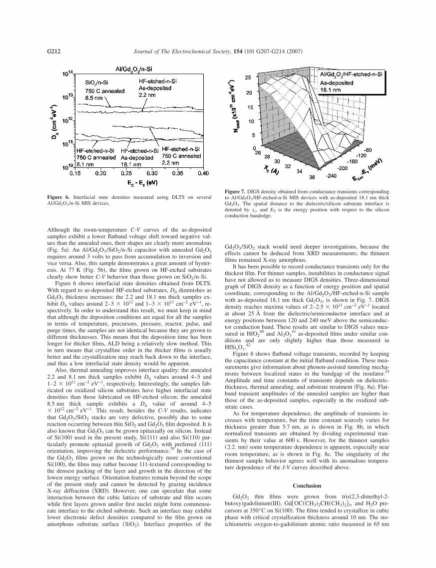
It has been possible to record conductance transients only for thethickest film. For thinner samples, instabilities in conductance signalhave not allowed us to measure DIGS densities. Three-dimensionalgraph of DIGS density as a function of energy position and spatialcoordinate, corresponding to the Al/Gd2O3/HF-etched-n-Si samplewith as-deposited 18.1 nm thick Gd2O3, is shown in Fig. 7. DIGSdensity reaches maxima values of 2–2.5 � 1011 cm−2 eV−1 locatedat about 25 Å from the dielectric/semiconductor interface and atenergy positions between 120 and 240 meV above the semiconduc-tor conduction band. These results are similar to DIGS values mea-sured in HfO2
40 and Al2O341 as-deposited films under similar con-
ditions and are only slightly higher than those measured inHfSixOy.
42
Figure 8 shows flatband voltage transients, recorded by keepingthe capacitance constant at the initial flatband condition. These mea-surements give information about phonon-assisted tunneling mecha-nisms between localized states in the bandgap of the insulator.24
Amplitude and time constants of transients depends on dielectric-thickness, thermal annealing, and substrate treatment �Fig. 8a�. Flat-band transient amplitudes of the annealed samples are higher thanthose of the as-deposited samples, especially in the oxidized sub-strate cases.
As for temperature dependence, the amplitude of transients in-creases with temperature, but the time constant scarcely varies forthickness greater than 5.7 nm, as is shown in Fig. 8b, in whichnormalized transients are obtained by dividing experimental tran-sients by their value at 600 s. However, for the thinnest samples�2.2. nm� some temperature dependence is apparent, especially nearroom temperature, as is shown in Fig. 8c. The singularity of thethinnest sample behavior agrees well with its anomalous tempera-ture dependence of the I-V curves described above.
Conclusion
Gd2O3 thin films were grown from tris�2,3-dimethyl-2-butoxy�gadolinium�III�, Gd�OC�CH3�2CH�CH3�2�3, and H2O pre-cursors at 350°C on Si�100�. The films tended to crystallize in cubicphase with critical crystallization thickness around 10 nm. The sto-ichiometric oxygen-to-gadolinium atomic ratio measured in 65 nm
Figure 7. DIGS density obtained from conductance transients correspondingto Al/Gd2O3/HF-etched-n-Si MIS devices with as-deposited 18.1 nm thickGd2O3. The spatial distance to the dielectric/silicon substrate interface isdenoted by xc, and ET is the energy position with respect to the siliconconduction bandedge.

G213Journal of The Electrochemical Society, 154 �10� G207-G214 �2007� G213
thick film was close to 1.4 ± 0.5, allowing the oxygen deficiency inthe films. The contents of residual hydrogen and carbon reached1.0 ± 0.5 and 0.6 ± 0.3 atom %, respectively.
Unannealed Gd O films on HF-etched Si exhibit better charac-
Figure 8. �a� Flatband transients, measured at 300 K, corresponding to sev-eral Al/Gd2O3/HF-etched n-Si capacitors with 2.2 and 8.1 nm thick Gd2O3films. �b� Normalized flatband transients, measured at temperatures between160 and 300 K, corresponding to capacitors with 8.1 nm and �c� 2.2 nmthick Gd2O3 films annealed at 750°C.
2 3
teristics than those deposited on SiO2/Si, in terms of leakage currentand flatband voltage. In this regard, the films possessed electricalcharacteristics noticeably different from more conventional high-permittivity materials, e.g., HfO2. Thermal annealing improvesAl/Gd2O3/HF-etched Si samples in terms of Dit but leads to highervalues of leakage current and flatband voltage. However, thermalannealing improves I-V characteristics but raises flatband voltage ofAl/Gd2O3/SiO2/Si samples. Both the interfacial state density andthe flatband voltage shift value decreases when the oxide thicknessof as-deposited Al/Gd2O3/HF-etched Si samples increases.DIGS values obtained for the 18 nm thick unannealedAl/Gd2O3/HF-etched Si sample are very similar to those measuredin HfO2 film-based MIS structures. Flatband transient amplitudesincrease when thermal annealing is applied, both in samples fabri-cated on oxidized and on HF-etched substrates.
Acknowledgments
The study was partially supported by the local government �Juntade Castilla y León� under grant no. VA018A06 and by the SpanishTEC2005 under grant no. 05101/MIC. The authors are indebted toDr. Kai Arstila for the ERDA results.
Universidad de Valladolid assisted in meeting the publication costs ofthis article.
References1. K. J. Hubbard and D. G. Schlom, J. Mater. Res., 11, 2757 �1996�.2. J. Robertson, J. Vac. Sci. Technol. B, 18, 1785 �2000�.3. M. Leskelä and M. Ritala, J. Solid State Chem., 171, 170 �2003�.4. M. Leskelä, K. Kukli, and M. Ritala, J. Alloys Compd., 418, 27 �2006�.5. M. Hong, A. R. Kortan, J. Kwo, J. P. Mannaerts, J. J. Krajewski, Z. H. Lu, K. C.
Hsieh, and K. Y. Cheng, J. Vac. Sci. Technol. B, 18, 1688 �2000�.6. J. Kwo, M. Hong, A. R. Kortan, K. T. Queeney, Y. J. Chabal, J. P. Mannaerts, T.
Boone, J. J. Krajewski, A. M. Sergent, and J. M. Rosamilia, Appl. Phys. Lett., 77,130 �2000�.
7. M. Hong, M. Passlack, J. P. Mannaerts, J. Kwo, S. N. G. Chu, N. Moriya, S. Y.Hou, and V. J. Fratello, J. Vac. Sci. Technol. B, 14, 2297 �1996�.
8. M. Hong, J. Kwo, A. R. Kortan, J. P. Mannaerts, and A. M. Sergent, Science, 283,1897 �1999�.
9. J. Kwo, M. Hong, A. R. Kortan, K. L. Queeny, Y. J. Chapal, R. L. Opila, Jr., D. A.Muller, S. N. G. Chu, B. J. Sapjeta, T. S. Lay, et al., J. Appl. Phys., 89, 3920�2001�.
10. M. P. Singh, C. S. Thakur, K. Shalini, S. Banerjee, N. Bhat, and S. A. Shivashan-kar, J. Appl. Phys., 96, 5631 �2004�.
11. T. M. Pang, C. S. Liao, H. H. Hsu, C. L. Chen, and J. C. Wang, Appl. Phys. Lett.,87, 262908 �2005�.
12. S. A. Park, Y. S. Roh, Y. K. Kim, J. H. Baeck, M. Noh, K. Jeong, M. H. Cho, C.H. Chang, M. K. Joo, T. G. Kim, et al., J. Appl. Phys., 98, 024906 �2005�.
13. L. Z. Hsieh, H. H. Ko, P. Y. Kuei, L. B. Chang, and M. J. Jeng, J. Appl. Phys., 98,076110 �2005�.
14. A. C. Jones, H. C. Aspinall, P. R. Chalker, R. J. Potter, K. Kukli, A. Rahtu, M.Ritala, and M. Leskelä, J. Mater. Chem., 14, 3101 �2004�.
15. H. Iwai, S. Ohmi, S. Akama, C. Ohsima, I. Kashiwagi, A. Kikuchi, J. Taguchi, H.Yamamoto, I. Ueda, A. Kuriyama, et al., in Physics and Technology of High-k GateDielectrics I, S. Kar, D. Misra, R. Singh, and F. Gonzalez, Editors, PV 2002-28, p.27, The Electrochemical Society Proceedings Series, Pennington, NJ �2002�.
16. J. Päiväsaari, M. Putkonen, and L. Niinistö, Thin Solid Films, 472, 275 �2005�.17. T. Suntola, Thin Solid Films, 216, 84 �1992�.18. D. V. Lang, J. Appl. Phys., 45, 3023 �1974�.19. M. Schulz and N. M. Johnson, Appl. Phys. Lett., 31, 622 �1977�.20. L. He, H. Hasegawa, T. Sawada, and H. Ohno, J. Appl. Phys., 63, 2120 �1998�.21. T. Hashizume, H. Hasegawa, R. Riemenschneider, and H. L. Hartnagel, Jpn. J.
Appl. Phys., Part 1, 33, 727 �1994�.22. S. Dueñas, R. Peláez, H. Castán, R. Pinacho, L. Quintanilla, J. Barbolla, I. Mártil,
and G. González-Díaz, Appl. Phys. Lett., 71, 826 �1997�.23. H. Castán, S. Dueñas, J. Barbolla, E. Redondo, N. Blanco, I. Mártil, and G.
González-Díaz, Microelectron. Reliab., 40, 845 �2000�.24. S. Dueñas, H. Castán, H. García, L. Bailón, K. Kukli, M. Ritala, and M. Leskelä,
Microelectron. Reliab., 47, 653 �2007�.25. B. O. Cho, J. Wang, L. Sha, and J. P. Chang, Appl. Phys. Lett., 80, 1052 �2002�.26. N. Novkovski and E. Atanassova, Appl. Phys. A, 83, 435 �2006�.27. W. Yang, J. Marino, A. Monson, and C. A. Wolden, Semicond. Sci. Technol., 21,
1573 �2006�.28. N. Novkoski, Semicond. Sci. Technol., 21, 945 �2006�.29. C. Zhao, T. Witters, B. Brijs, H. Bender, O. Richard, M. Caymax, T. Heeg, J.
Schubert, V. V. Afanas’ev, A. Stesmans, et al., Appl. Phys. Lett., 86, 132903�2005�.
30. N. A. Hegab and H. E. Atya, J. Ovonic Research., 2, 21 �2006�.31. Y. Kim, S. Ohmi, K. Tsutsui, and H. Iwai, Jpn. J. Appl. Phys., Part 1, 44, 6A and
4032 �2005�.32. S. Kar and R. Singh, in Physics and Technology of High-k Gate Dielectrics I, S.

G214 Journal of The Electrochemical Society, 154 �10� G207-G214 �2007�G214
Kar, D. Misra, R. Singh, and F. Gonzalez, Editors, PV 2002-28, p. 13, The Elec-trochemical Society Proceedings Series, Pennington, NJ �2002�.
33. G. A. Niklasson and K. Brantervik, J. Appl. Phys., 59, 980 �1986�.34. M. Wagner, T. Heeg, J. Schubert, St. Lenk, S. Mantl, C. Zhao, M. Caymax, and S.
De Gendt, Appl. Phys. Lett., 88, 172901 �2006�.35. W. J. Zhu, M. Khare, J. Snare, P. R. Varekamp, S. H. Ku, P. Agnello, T. C. Chen,
and T. P. Ma, Proceedings of the International Symposium on VLSI TechnologySystems Applications, Hsinchu, Taiwan, p. 212 �2001�.
36. A. Laha, E. Bugiel, H. J. Osten, and A. Fissel, Appl. Phys. Lett., 88, 172107�2006�.
37. R. L. Nigro, V. Raineri, C. Bondiorno, R. Toro, G. Malandrino, and I. L. Fragala,
Appl. Phys. Lett., 83, 129 �2003�.38. M. Czernohorsky, E. Bugiel, H. J. Osten, A. Fissel, and O. Kirfel, Appl. Phys. Lett.,
88, 152905 �2006�.39. A. Laha, H. J. Osten, and A. Fissel, Appl. Phys. Lett., 89, 143514 �2006�.40. S. Dueñas, H. Castán, H. García, J. Barbolla, K. Kukli, J. Aarik, and A. Aidla,
Semicond. Sci. Technol., 19, 1141 �2004�.41. S. Dueñas, H. Castán, H. García, A. de Castro, L. Bailón, K. Kukli, A. Aidla, J.
Aarik, H. Mändar, T. Uustare, et al., J. Appl. Phys., 99, 054902 �2006�.42. S. Dueñas, H. Castán, H. García, L. Bailón, K. Kukli, M. Ritala, M. Leskelä, M.
Rooth, O. Wilhelmsson, and A. Harsta, J. Appl. Phys., 100, 094107 �2006�.
Copyright © 2022 FDOKUMEN