Structure of diamond polycrystalline films deposited on silicon substrates
6
This article appeared in a journal published by Elsevier. The attached copy is furnished to the author for internal non-commercial research and education use, including for instruction at the authors institution and sharing with colleagues. Other uses, including reproduction and distribution, or selling or licensing copies, or posting to personal, institutional or third party websites are prohibited. In most cases authors are permitted to post their version of the article (e.g. in Word or Tex form) to their personal website or institutional repository. Authors requiring further information regarding Elsevier’s archiving and manuscript policies are encouraged to visit: http://www.elsevier.com/copyright
-
Upload
independent -
Category
Documents
-
view
4 -
download
0
Transcript of Structure of diamond polycrystalline films deposited on silicon substrates
This article appeared in a journal published by Elsevier. The attachedcopy is furnished to the author for internal non-commercial researchand education use, including for instruction at the authors institution
and sharing with colleagues.
Other uses, including reproduction and distribution, or selling orlicensing copies, or posting to personal, institutional or third party
websites are prohibited.
In most cases authors are permitted to post their version of thearticle (e.g. in Word or Tex form) to their personal website orinstitutional repository. Authors requiring further information
regarding Elsevier’s archiving and manuscript policies areencouraged to visit:
http://www.elsevier.com/copyright

Author's personal copy
Structure of diamond polycrystalline films deposited on silicon substrates
E. Staryga a,*, G.W. Bak a, K. Fabisiak b, L. Klimek c, A. Rylski c, A. Olborska c, M. Kozanecki d, J. Grabarczyk c
a Institute of Physics, Technical University of Łód�z, Wólcza�nska 219, 93-005 Łód�z, Polandb Institute of Physics, Kazimierz Wielki University, Weyssenhoffa Sq.11, 85-072 Bydgoszcz, Polandc Institute of Materials Science and Engineering, Technical University of Łód�z, Stefanowskiego 1/15, 90-924 Łód�z, PolanddDept. of Molecular Physics, Technical Univ. of Łód�z, _Zeromskiego 116, 90-924 Łód�z, Poland
Keywords:Diamond filmsResidual stressEBSDRaman spectroscopy
a b s t r a c t
The article presents results of structural studies of polycrystalline diamond thin films deposited by hotfilament CVD on silicon substrates. The films were characterized using Scanning Electron Microscopy(SEM), Raman Spectroscopy (RS), Electron Backscattered Diffraction (EBSD), Energy Dispersive Spec-troscopy (EDS) and Secondary Ion Mass Spectroscopy (SIMS). Both the EBSD patterns and Raman spectraconfirm that the grains visible in the electron micrographs are diamond micro-crystallites. The residualstress in the films is found to be in the range between �4.29 GPa and �0.56 GPa depending on thesample thickness. No evidence of lonsdalite and graphite has been registered in the polycrystallinematerial of the investigated samples. Evidence of the existence of silicon carbide at the diamond/siliconinterface is presented. It is also suggested that an amorphous carbonaceous film covers the silicon surfacein the regions of holes in the thin diamond layers.
� 2010 Elsevier Ltd. All rights reserved.
1. Introduction
Despite the fact that there are many results of structuralinvestigations of diamond and diamond-like carbon films depos-ited on silicon substrates (see e.g. Refs. [1,2]), the EBSD investiga-tions of diamond films are not very common. Only a few papersconcerning the EBSD studies of diamond films are available [3e6].The papers focus on the structure of films on a micro-scale. In thispaper detailed investigations of the structure of thin diamond filmsdeposited on silicon substrates using EBSD and other techniquesare presented. The residual stress in the films deposited on vari-ously oriented silicon substrates was calculated in order to deter-mine the relationship between the substrate orientation and thestress value. It is also shown that silicon carbide (SiC) exists at thesilicon/diamond interface. This should be taken into account whenthe electrical properties of silicon/diamond junctions are discussed.
2. Experimental
Diamond films were grown on silicon substrates using the hotfilament chemical vapour deposition (HF CVD) method. A mixture
of methanol and hydrogenwas used for the deposition process. Theamount of methanol was changed in the range between 1.0% and2.5%, the total gas flow rate was between 100 sccm and 150 sccmand the gas pressure in the reaction chamber was changed between50 mbar and 60 mbar (Table 1) and the substrate temperature was1100 K. The filmswere deposited on n-type silicon substrates whichwere cut out from a single crystal silicon wafer oriented (100) or(111). The details of the deposition system used and typical depo-sition conditions are described elsewhere [7].
The quality of crystalline structure of diamond films wasevaluated using Raman Spectroscopy. The Raman spectra wererecorded at room temperature in backscattering geometry usinga Jobin-Yvon T64000 Raman micro-spectrometer. The 514.5 nmline from an Argon laser was used for excitation. Morphology ofthe films was examined in a scanning electron microscope (SEM,Hitachi S 3000N). Electron backscattered diffraction (EBSD) [8] ofthe investigated diamond films was carried out using the EBSDThermoNORAN equipment attached to the SEM. In order toidentify the chemical composition in selected areas of thesamples an Energy Dispersive Spectrometer (ThermoNORAN) wasused.
In order to find the spatial distribution of chemical elements inthe films Secondary Ion Mass Spectroscopy (SIMS) measurementswere also carried out. The measurements were carried out witha Secondary Ion Mass Spectrometer (ToF-SIMS IV, Ion-ToF GmbH,Muenster Germany) with 69Gaþ primary ion source and time-of-
* Corresponding author. Tel.: þ48 42 631 36 51; fax: þ48 42 631 36 39.E-mail address: [email protected] (E. Staryga).
Contents lists available at ScienceDirect
Vacuum
journal homepage: www.elsevier .com/locate/vacuum
0042-207X/$ e see front matter � 2010 Elsevier Ltd. All rights reserved.doi:10.1016/j.vacuum.2010.01.025
Vacuum 85 (2010) 518e522
Author's personal copy
flight (ToF) secondary ion mass analyzer with high mass resolutionm/Dm ¼ 7500 at m/z ¼ 29.
3. Results and discussion
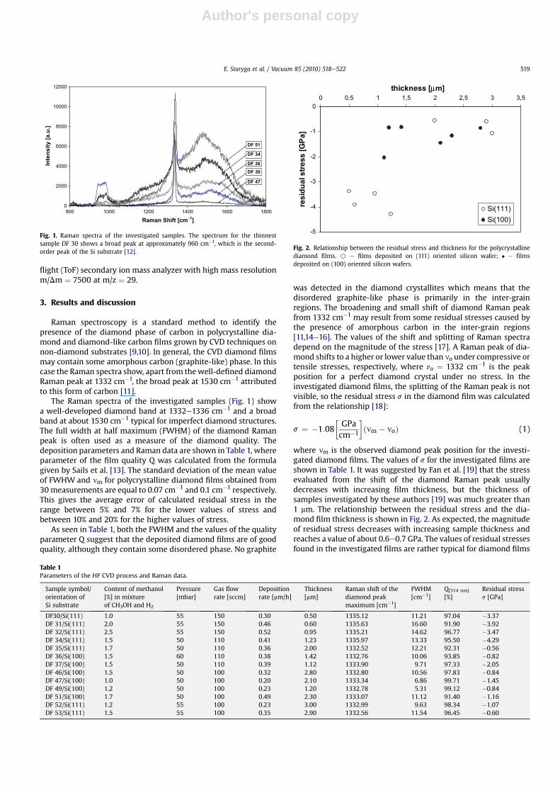
Raman spectroscopy is a standard method to identify thepresence of the diamond phase of carbon in polycrystalline dia-mond and diamond-like carbon films grown by CVD techniques onnon-diamond substrates [9,10]. In general, the CVD diamond filmsmay contain some amorphous carbon (graphite-like) phase. In thiscase the Raman spectra show, apart from thewell-defined diamondRaman peak at 1332 cm�1, the broad peak at 1530 cm�1 attributedto this form of carbon [11].
The Raman spectra of the investigated samples (Fig. 1) showa well-developed diamond band at 1332e1336 cm�1 and a broadband at about 1530 cm�1 typical for imperfect diamond structures.The full width at half maximum (FWHM) of the diamond Ramanpeak is often used as a measure of the diamond quality. Thedeposition parameters and Raman data are shown in Table 1, whereparameter of the film quality Q was calculated from the formulagiven by Sails et al. [13]. The standard deviation of the mean valueof FWHW and nm for polycrystalline diamond films obtained from30measurements are equal to 0.07 cm�1 and 0.1 cm�1 respectively.This gives the average error of calculated residual stress in therange between 5% and 7% for the lower values of stress andbetween 10% and 20% for the higher values of stress.
As seen in Table 1, both the FWHM and the values of the qualityparameter Q suggest that the deposited diamond films are of goodquality, although they contain some disordered phase. No graphite
was detected in the diamond crystallites which means that thedisordered graphite-like phase is primarily in the inter-grainregions. The broadening and small shift of diamond Raman peakfrom 1332 cm�1 may result from some residual stresses caused bythe presence of amorphous carbon in the inter-grain regions[11,14e16]. The values of the shift and splitting of Raman spectradepend on the magnitude of the stress [17]. A Raman peak of dia-mond shifts to a higher or lower value than no under compressive ortensile stresses, respectively, where no ¼ 1332 cm�1 is the peakposition for a perfect diamond crystal under no stress. In theinvestigated diamond films, the splitting of the Raman peak is notvisible, so the residual stress s in the diamond film was calculatedfrom the relationship [18]:
s ¼ �1:08�GPacm�1
�ðnm � noÞ (1)
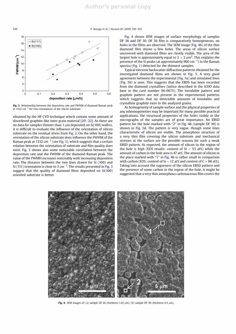
where nm is the observed diamond peak position for the investi-gated diamond films. The values of s for the investigated films areshown in Table 1. It was suggested by Fan et al. [19] that the stressevaluated from the shift of the diamond Raman peak usuallydecreases with increasing film thickness, but the thickness ofsamples investigated by these authors [19] was much greater than1 mm. The relationship between the residual stress and the dia-mond film thickness is shown in Fig. 2. As expected, the magnitudeof residual stress decreases with increasing sample thickness andreaches a value of about 0.6e0.7 GPa. The values of residual stressesfound in the investigated films are rather typical for diamond films
0
2000
4000
6000
8000
10000
12000
800 1000 1200 1400 1600 1800
Raman Shift [cm-1
]
].
u.
a[
y
ti
sn
et
nI
DF 51
DF 34
DF 36
DF 30
DF 47
Fig. 1. Raman spectra of the investigated samples. The spectrum for the thinnestsample DF 30 shows a broad peak at approximately 960 cm�1, which is the second-order peak of the Si substrate [12].
Table 1Parameters of the HF CVD process and Raman data.
Sample symbol/orientation ofSi substrate
Content of methanol[%] in mixtureof CH3OH and H2
Pressure[mbar]
Gas flowrate [sccm]
Depositionrate [mm/h]
Thickness[mm]
Raman shift of thediamond peakmaximum [cm�1]
FWHM[cm�1]
Q[514 nm]
[%]Residual stresss [GPa]
DF30/Si(111) 1.0 55 150 0.30 0.50 1335.12 11.21 97.04 �3.37DF 31/Si(111) 2.0 55 150 0.46 0.60 1335.63 16.60 91.90 �3.92DF 32/Si(111) 2.5 55 150 0.52 0.95 1335.21 14.62 96.77 �3.47DF 34/Si(111) 1.5 50 110 0.41 1.23 1335.97 13.33 95.50 �4.29DF 35/Si(111) 1.7 50 110 0.36 2.00 1332.52 12.21 92.31 �0.56DF 36/Si(100) 1.5 60 110 0.38 1.42 1332.76 10.06 93.85 �0.82DF 37/Si(100) 1.5 50 110 0.39 1.12 1333.90 9.71 97.33 �2.05DF 46/Si(100) 1.5 50 100 0.32 2.80 1332.80 10.56 97.83 �0.84DF 47/Si(100) 1.0 50 100 0.20 2.10 1333.34 6.86 99.71 �1.45DF 49/Si(100) 1.2 50 100 0.23 1.20 1332.78 5.31 99.12 �0.84DF 51/Si(100) 1.7 50 100 0.49 2.30 1333.07 11.12 91.40 �1.16DF 52/Si(111) 1.2 55 100 0.23 3.00 1332.99 9.63 98.34 �1.07DF 53/Si(111) 1.5 55 100 0.35 2.90 1332.56 11.54 96.45 �0.60
-5
-4
-3
-2
-1
00 0,5 1 1,5 2 2,5 3 3,5
thickness [µm]
]a
PG
[ s
se
rt
s la
udi
se
r Si(111)Si(100)
Fig. 2. Relationship between the residual stress and thickness for the polycrystallinediamond films. B e films deposited on (111) oriented silicon wafer; � e filmsdeposited on (100) oriented silicon wafers.
E. Staryga et al. / Vacuum 85 (2010) 518e522 519
Author's personal copy
obtained by the HF CVD technique which contain some amount ofdisordered graphite-like inter-grain material [20e22]. As there areno data for samples thinner than 1 mmdeposited on Si(100) wafers,it is difficult to evaluate the influence of the orientation of siliconsubstrate on the residual stress from Fig. 2. On the other hand, theorientation of the silicon substrate does influence the FWHM of theRaman peak at 1332 cm�1 (see Fig. 3), which suggests that a certainrelation between the orientation of substrate and film quality doesexist. Fig. 3 shows also some noticeable correlation between thedeposition rate and the FWHM of the diamond Raman peak. Thevalue of the FWMH increases noticeably with increasing depositionrate. The distance between the two lines drawn for Si (100) andSi (111) orientation is close to 3 cm�1. The results presented in Fig. 3suggest that the quality of diamond films deposited on Si(100)oriented substrate is better.
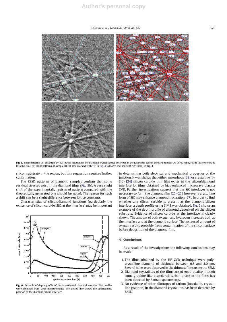
Fig. 4 shows SEM images of surface morphology of samplesDF 36 and DF 30. DF 36 film is comparatively homogeneous, noholes in the films are observed. The SEM image (Fig. 4b) of the thindiamond film shows a few holes. The areas of silicon surfaceuncovered with diamond films are clearly visible. The area of thelargest hole is approximately equal to 2 � 2 mm2. This explains thepresence of the Si peaks (at approximately 960 cm�1) in the Ramanspectra (Fig. 1) detected for the thinnest samples.
Typical electron backscatter diffraction patterns obtained for theinvestigated diamond films are shown in Fig. 5. A very goodagreement between the experimental (Fig. 5a) and simulated lines(Fig. 5b) is seen. This suggests that the EBDS has been recordedfrom the diamond crystallites (lattice described in the ICDD database in the card number 06-0675). The lonsdalite pattern andgraphite pattern are not present in the experimental patternswhich suggests that no detectable amounts of lonsdalite andcrystalline graphite exist in the analyzed grains.
As homogeneity of sample surface and the physical properties ofany inhomogeneities may be important for many possible practicalapplications, the structural properties of the holes visible in themicrographs of the samples are of great importance. An EBSDpattern for the hole marked with “2” in Fig. 4b (sample DF 30) isshown in Fig. 5d. The pattern is very vague, though some linescharacteristic of silicon are visible. The amorphous structure ofa very thin film covering the silicon substrate and mechanicalstresses at the surface are the possible reasons for such a weakEBSD pattern. As expected, the amount of silicon in the region ofthe hole is high (EDS results: content of Si ¼ 53 at%) while theamount of carbon in the hole area is 47 at%. The amount of silicon inthe place marked with “1” in Fig. 4b is rather small in comparisonwith carbon (EDS: content of Si¼ 12 at% and content of C¼ 88 at%).Taking into account the vagueness of the silicon EBSD pattern andthe presence of some carbon in the region of the hole, it might besuggested that a very thin amorphous carbonaceous film covers the
2
4
6
8
10
12
14
16
18
0 0,1 0,2 0,3 0,4 0,5 0,6
deposition rate [µm/h]
mc
[M
HW
F1
-
]
Si(111)Si(100)
Fig. 3. Relationship between the deposition rate and FWHM of diamond Raman peakat 1332 cm�1 for two orientations of the silicon substrate.
Fig. 4. SEM images of: (a) sample DF 36 (thickness 1.42 mm); (b) sample DF 30 (thickness 0.5 mm).
E. Staryga et al. / Vacuum 85 (2010) 518e522520
Author's personal copy
silicon substrate in the region, but this suggestion requires furtherconfirmation.
The EBSD patterns of diamond samples confirm that someresidual stresses exist in the diamond films (Fig. 5b). A very slightshift of the experimentally registered pattern compared with thetheoretically generated one should be noted. The reason for sucha shift can be a slight difference between lattice constants.
Characteristics of silicon/diamond junctions (particularly theexistence of silicon carbide, SiC, at the interface) may be important
in determining both electrical and mechanical properties of thejunction. It was shown that either amorphous [23] or crystalline (b-SiC) [24] silicon carbide thin film exists in the silicon/diamondinterface for films obtained by bias-enhanced microwave plasmaCVD. Further investigations suggest that the SiC interlayer is notnecessary to form the diamond film [25e27], however a crystallineform of SiC may enhance diamond nucleation [27]. In order to findwhether any silicon carbide is present at the diamond/siliconinterface, a depth profile using SIMS was obtained. Fig. 6 shows anexample of the depth profile of diamond deposited on the siliconsubstrate. Evidence of silicon carbide at the interface is clearlyshown. The amount of both oxygen and hydrogen increases both atthe interface and at the diamond surface. The increased amount ofoxygen results probably from contamination of the silicon surfacebefore deposition of the diamond film.
4. Conclusions
As a result of the investigations the following conclusions maybe made:
1. The films obtained by the HF CVD technique were poly-crystalline diamond of thickness between 0.5 and 3.0 mm.Several holeswere observed in the thinnestfilms using the SEM.
2. Diamond crystallites of the films are of good quality, thoughsome graphite-like disordered carbon phase in the films hasbeen detected by Raman spectroscopy.
3. No evidence of other allotropes of carbon (lonsdalite, crystal-line graphite) in the diamond crystallites has been detected byEBSD.
Fig. 5. EBSD patterns: (a) of sample DF 32; (b) the solution for the diamond crystal (lattice described in the ICDD data base in the card number 06-0675, cubic, Fd3m, lattice constant0.35667 nm); (c) EBSD patterns of sample DF 30 area marked with “1” in Fig. 4; (d) area marked with “2” (hole) in Fig. 4.
Fig. 6. Example of depth profile of the investigated diamond samples. The profileswere obtained from SIMS measurements. The dotted line shows the approximateposition of the diamond/silicon interface.
E. Staryga et al. / Vacuum 85 (2010) 518e522 521

Author's personal copy
4. The value of stress in the investigated samples changes in therange between �4.29 GPa and �0.56 GPa. The stress decreasesto a magnitude of approximately 0.6 GPae0.7 GPa with theincreasing sample thickness. The orientation of the siliconsubstrate influences the structure of the diamond films. Dia-mond films deposited on Si(100) prove to be of better quality.
5. The existence of silicon carbide at diamond/silicon interfacehas been confirmed by SIMS measurements, but there is noevidence of crystalline silicon carbide in the region of the holesin the thin coatings.
Acknowledgments
This work was partially supported by development grantN R050045 06 from the founds of Polish Ministry of Science andHigher Education in years 2010e2012.
References
[1] Robertson J. Mater Sci Eng R 2002;37:129e281.[2] Donato MG, Faggio G, Marinelli M, Messina G, Milani E, Paoletti A, et al. Eur
Phys J B 2001;20:133e9.[3] Chen HW, Rudolph V. Diamond Relat Mater 2003;12:1633e9.[4] Schreck M, Grunick C, Haug C, Brenn R, Stritzker B. Diamond Relat Mater
2002;11:487e92.[5] Mao W, Zhu H, Chen L, Feng H. Mater Sci Technol 2005;21:1383.
[6] Su YH, Chang L, Chen HG, Yan JK, Chou T. Diamond Relat Mater2005;14:1753e6.
[7] Fabisiak K, Szreiber M, Uniszkiewicz C, Runka T, Kasprowicz D. Opt Appl2009;XXXIX:833e7.
[8] Schwartz AJ. Electron backscatter diffraction in materials science.Netherlands: Kluwer Academic Publishers; 2001. Group.
[9] Knight DS, White WB. J Mater Res 1989;4:385e93.[10] Izák T, Marton M, Varga M, Vojs M, Veselý M, Redhammer R, et al. Vacuum
2009;84:49e52.[11] Prelas M, Popovici G, Bigelow LK. Handbook of industrial diamonds and dia-
mond films. New York: Marcel Dekker; 1998.[12] Jung HS, Park HH. Diamond Relat Mater 2003;12:1373e7.[13] Sails SR, Gardiner DJ, Bowden M, Savage J, Rodway D. Diamond Relat Mater
1996;5:589e91.[14] Pandey M, Cunha RD, Tyagi AK. J Alloys Compd 2002;333:260e5.[15] Chen KH, Lai YL, Lin JC, Song KJ, Chen LC, Haug CY. Diamond Relat Mater
1995;4:460e3.[16] Windischmann H, Gray KJ. Diamond Relat Mater 1995;4:837e42.[17] Ager III JW, Drory MD. Phys Rev B 1993;48:2601e7.[18] Ralchenko VG, Smolin AA, Pereverzev VG, Obraztsova ED, Korotoushenko KG,
Konov VI, et al. Diamond Relat Mater 1995;4:754e8.[19] Fan QH, Fernandes A, Pereira E, Gracio J. Diamond Relat Mater
1999;8:645e50.[20] Kromka A, Breza J, Kadle�ciková M, Janik J, Balon F. Carbon 2005;43:425e9.[21] Nakamura Y, Sakagami S, Amamoto Y, Watanabe Y. Thin Solid Films
1997;308e309:249e53.[22] Kim JG, Yu J. Jpn J Appl Phys 1998;37:L890e3.[23] Stoner BR, Ma G-HM, Wolter SD, Glass T. Phys Rev B 1992;45:11067e84.[24] Wiliams BE, Glass JT. J Mater Res 1989;4:373e84.[25] Jiang X, Jia CL. Appl Phys Lett 1995;67:1197e9.[26] Zhang RQ, Wang WL, Estevea J, Bertran E. Thin Solid Films 1998;317:6e9.[27] Jiang X, Schiffmann K, Klages C-P. Phys Rev B 1994;50:8402e10.
E. Staryga et al. / Vacuum 85 (2010) 518e522522