Damage evaluation in graphene underlying atomic layer deposition dielectrics
12
1 SCIENTIFIC REPORTS | 5:13523 | DOI: 10.1038/srep13523 www.nature.com/scientificreports Damage evaluation in graphene underlying atomic layer deposition dielectrics Xiaohui Tang 1 , Nicolas Reckinger 2,3 , Olivier Poncelet 1 , Pierre Louette 3 , Ferran Ureña 1 , Hosni Idrissi 5,6 , Stuart Turner 5 , Damien Cabosart 4 , Jean-François Colomer 2,3 , Jean- Pierre Raskin 1 , Benoit Hackens 4 & Laurent A. Francis 1 Based on micro-Raman spectroscopy (μRS) and X-ray photoelectron spectroscopy (XPS), we study the structural damage incurred in monolayer (1L) and few-layer (FL) graphene subjected to atomic- layer deposition of HfO 2 and Al 2 O 3 upon different oxygen plasma power levels. We evaluate the damage level and the influence of the HfO 2 thickness on graphene. The results indicate that in the case of Al 2 O 3 /graphene, whether 1L or FL graphene is strongly damaged under our process conditions. For the case of HfO 2 /graphene, μRS analysis clearly shows that FL graphene is less disordered than 1L graphene. In addition, the damage levels in FL graphene decrease with the number of layers. Moreover, the FL graphene damage is inversely proportional to the thickness of HfO 2 film. Particularly, the bottom layer of twisted bilayer (t-2L) has the salient features of 1L graphene. Therefore, FL graphene allows for controlling/limiting the degree of defect during the PE-ALD HfO 2 of dielectrics and could be a good starting material for building field effect transistors, sensors, touch screens and solar cells. Besides, the formation of Hf-C bonds may favor growing high- quality and uniform-coverage dielectric. HfO 2 could be a suitable high-K gate dielectric with a scaling capability down to sub-5-nm for graphene-based transistors. One of the most explored application domains for graphene is nanoelectronics because of its high carrier mobility and atomic thickness 1,2 . However, gate dielectric deposition is an important challenge for trans- ferring graphene transistors from laboratory level to industrial production. Dielectric or metal deposition induces defects in monolayer (1L) graphene and at the interface between dielectric and few-layer (FL) graphene 3 . e carrier mobility is very sensitive to the graphene lattice defects and interface quality. It has indeed been reported that the carrier mobility of suspended graphene is significantly higher than that of graphene lying over a silicon dioxide (SiO 2 ) substrate 4 due to corrugation, traps at the interface and fixed charges in the dielectric layer. erefore, it is a crucial task to grow metal-oxide dielectric films on graphene with minimum damage/degradation into the graphene lattice. Although physical vapor deposition (such as magnetron sputtering), widely used in the semiconductor industry, can provide high deposition rates and preserve film stoichiometry, it generates extensive dam- age in graphene from high energy sputtered atoms 5 . Researchers mostly choose atomic layer deposition 1 ICTEAM Institute, Université catholique de Louvain, Place du Levant 3, 1348 Louvain-la-Neuve, Belgium. 2 Research Group on Carbon Nanostructures (CARBONNAGe), University of Namur, Rue de Bruxelles 61, 5000 Namur, Belgium. 3 Department of Physics, Research Center in Physics of Matter and Radiation (PMR), University of Namur, Rue de Bruxelles 61, 5000 Namur, Belgium. 4 NAPS/IMCN, Université catholique de Louvain, 2 Chemin du Cyclotron, 1348 Louvain-la- Neuve, Belgium. 5 Electron Microscopy for Materials Science (EMAT), Department of Physics, University of Antwerp, Groenenborgerlaan 171, B-2020 Antwerp, Belgium. 6 Institute of Mechanics, Materials and Civil Engineering, Université catholique de Louvain, Place Sainte Barbe 2, B-1348 Louvain-la-Neuve, Belgium. Correspondence and requests for materials should be addressed to X.T. (email: xiaohui.tang@uclouvain. be) Received: 11 February 2015 Accepted: 27 July 2015 Published: 27 August 2015 OPEN
Transcript of Damage evaluation in graphene underlying atomic layer deposition dielectrics

1Scientific RepoRts | 5:13523 | DOi: 10.1038/srep13523
www.nature.com/scientificreports
Damage evaluation in graphene underlying atomic layer deposition dielectricsXiaohui Tang1, Nicolas Reckinger2,3, Olivier Poncelet1, Pierre Louette3, Ferran Ureña1, Hosni Idrissi5,6, Stuart Turner5, Damien Cabosart4, Jean-François Colomer2,3, Jean-Pierre Raskin1, Benoit Hackens4 & Laurent A. Francis1
Based on micro-Raman spectroscopy (μRS) and X-ray photoelectron spectroscopy (XPS), we study the structural damage incurred in monolayer (1L) and few-layer (FL) graphene subjected to atomic-layer deposition of HfO2 and Al2O3 upon different oxygen plasma power levels. We evaluate the damage level and the influence of the HfO2 thickness on graphene. The results indicate that in the case of Al2O3/graphene, whether 1L or FL graphene is strongly damaged under our process conditions. For the case of HfO2/graphene, μRS analysis clearly shows that FL graphene is less disordered than 1L graphene. In addition, the damage levels in FL graphene decrease with the number of layers. Moreover, the FL graphene damage is inversely proportional to the thickness of HfO2 film. Particularly, the bottom layer of twisted bilayer (t-2L) has the salient features of 1L graphene. Therefore, FL graphene allows for controlling/limiting the degree of defect during the PE-ALD HfO2 of dielectrics and could be a good starting material for building field effect transistors, sensors, touch screens and solar cells. Besides, the formation of Hf-C bonds may favor growing high-quality and uniform-coverage dielectric. HfO2 could be a suitable high-K gate dielectric with a scaling capability down to sub-5-nm for graphene-based transistors.
One of the most explored application domains for graphene is nanoelectronics because of its high carrier mobility and atomic thickness1,2. However, gate dielectric deposition is an important challenge for trans-ferring graphene transistors from laboratory level to industrial production. Dielectric or metal deposition induces defects in monolayer (1L) graphene and at the interface between dielectric and few-layer (FL) graphene3. The carrier mobility is very sensitive to the graphene lattice defects and interface quality. It has indeed been reported that the carrier mobility of suspended graphene is significantly higher than that of graphene lying over a silicon dioxide (SiO2) substrate4 due to corrugation, traps at the interface and fixed charges in the dielectric layer. Therefore, it is a crucial task to grow metal-oxide dielectric films on graphene with minimum damage/degradation into the graphene lattice.
Although physical vapor deposition (such as magnetron sputtering), widely used in the semiconductor industry, can provide high deposition rates and preserve film stoichiometry, it generates extensive dam-age in graphene from high energy sputtered atoms5. Researchers mostly choose atomic layer deposition
1ICTEAM Institute, Université catholique de Louvain, Place du Levant 3, 1348 Louvain-la-Neuve, Belgium. 2Research Group on Carbon Nanostructures (CARBONNAGe), University of Namur, Rue de Bruxelles 61, 5000 Namur, Belgium. 3Department of Physics, Research Center in Physics of Matter and Radiation (PMR), University of Namur, Rue de Bruxelles 61, 5000 Namur, Belgium. 4NAPS/IMCN, Université catholique de Louvain, 2 Chemin du Cyclotron, 1348 Louvain-la- Neuve, Belgium. 5Electron Microscopy for Materials Science (EMAT), Department of Physics, University of Antwerp, Groenenborgerlaan 171, B-2020 Antwerp, Belgium. 6Institute of Mechanics, Materials and Civil Engineering, Université catholique de Louvain, Place Sainte Barbe 2, B-1348 Louvain-la-Neuve, Belgium. Correspondence and requests for materials should be addressed to X.T. (email: [email protected])
Received: 11 February 2015
Accepted: 27 July 2015
Published: 27 August 2015
OPEN

www.nature.com/scientificreports/
2Scientific RepoRts | 5:13523 | DOi: 10.1038/srep13523
(ALD)6,7 for dielectric growth on graphene8. ALD allows for controlling the thickness and uniformity of the deposited films with atomic-level precision while avoiding physical damage of energized atoms to the surface. ALD techniques are classified into plasma (oxygen-based) and thermal (water-based) depo-sitions. Very few examples dealing with the former technique were reported. Only Nayfeh et al.9 demon-strated a graphene transistor for which aluminum oxide (Al2O3) gate dielectric was directly deposited on graphene by using a remote plasma-enhanced ALD (PE-ALD) process. Most of the reports are related to the latter method, because plasma is rather aggressive (especially using a direct plasma) and generally etches graphene10. It is well known that graphene is hydrophobic and inert. More specifically, graphene does not provide reactive nucleation sites for the precursors in thermal ALD11,12 since it does not display covalent bonds out of the plane. Therefore, growing high-quality and uniform-coverage dielectrics by thermal ALD requires a graphene pretreatment. Various approaches have been proposed: (i) graphene is chemically modified by fluorine13, ozone14, nitride plasma15,16, organic molecules17 or perylene tetra-carboxylic acid18,19; (ii) metal particles are deposited on graphene as appropriate nucleation layers20; (iii) self-assembled monolayers are used to template the direct growth of dielectrics21; (iv) graphene islands, serving as a seed layer, are generated by low-power plasma22. Some of these approaches are complicated and incompatible with the existing mainstream integrated circuit technology. More particularly, these approaches might cause undesirable side effects, such as: inducing defects, doping graphene, leaving seed layers, increasing the dielectric thickness, and degrading the dielectric properties. Two previous articles pointed out that graphene is possibly degraded by the pretreatment23,24. Alternatively, the ozone pretreatment has proved to be responsible for significant damage to graphene in high-temperature ther-mal ALD25.
In this work, we use mild plasma conditions to directly grow hafnium oxide (HfO2) and Al2O3 die-lectrics on graphene by PE-ALD. In our process, the graphene samples are placed away from the plasma source for outside of the glow discharge. The remote oxygen plasma with low ion bombardment avoids fast etching of graphene. Simultaneously, the reaction between graphene and the precursor still guaran-tees physical/chemical modification of graphene. Based on micro-Raman spectroscopy (μ RS) and X-ray photoelectron spectroscopy (XPS), we study the structural damage induced in 1L graphene underlying HfO2 and Al2O3 upon different oxygen plasma power levels. We evaluate the damage levels in AB-stacked bilayer (AB-2L), twisted bilayer (t-BL) and trilayer (3L) graphene (hereafter they are collectively referred to as FL) underlying HfO2 and Al2O3 for a fixed oxygen plasma power. We also investigate the influence of the HfO2 thickness on graphene with various layer numbers. The results indicate that in the case of Al2O3/graphene, both 1L and FL graphene are strongly damaged under the present process conditions. In the case of HfO2/graphene, μ RS analysis clearly shows that FL graphene presents much less disorder than 1L graphene. Moreover, the FL graphene damage decreases with the number of layers. Our results also reveal that an inverse dependence of FL graphene damage with increasing the thickness of HfO2 film. FL graphene allows for controlling/limiting the defect formation during the PE-ALD HfO2 process. Therefore, it could be a good starting material for applications such as graphene-based transistors and sensing devices26,27, since, presently, wafer-scale homogeneous FL graphene can been synthesized by chemical vapor deposition (CVD)28.
ResultsGraphene morphology observations by SEM, AFM, optical microscopy and TEM. Figure 1a–c show scanning electron microscopy images of atmospheric pressure chemical vapor deposition (APCVD) graphene on copper foils (see methods and the reference29 for more information about the graphene growth and transfer conditions). The different contrasts in the images correspond to the different graphene layer numbers. It can be seen that the 1L, 2L, and 3L graphene domains are hexagonal. An hexagon is the typical shape of graphene domains grown by APCVD30. In another article, the same group explored the shape variations versus the APCVD growth conditions. They explained the shape modulation by the competition between atom diffusion along graphene domain edges or corners and surface diffusion processes31. In addition, Fig. 1d presents an atomic force microscopy image of graphene transferred onto SiO2, in which 1L, 2L and 3L can be clearly seen. Figure 1e plots the profile of stacked graphene flakes along the A–B line, confirming that each graphene layer has a thickness of about 0.3 nm.
Figure 2a illustrates an optical microscopy image of as-transferred graphene on the SiO2/Si substrate, revealing that the graphene film is composed of isolated and contiguous hexagonal flakes of various layer numbers. Most of the hexagons are 1L. High-angle t-2L, AB-2L and 3L graphene hexagons are found in certain regions. As shown in Fig. 2b, graphene underlying the HfO2 dielectric film is still clearly visible. Figure 2c shows a cross-sectional high angle annular dark field scanning transmission electron microscopy (HAADF-STEM/Z-contrast) image of the HfO2/graphene/SiO2/Si stack, indicating the uni-form covering of graphene with the HfO2 film. No clustering or pinholes in the HfO2 film is observed.
Graphene structural damage evaluation by μRS. μ RS is a nondestructive method and is employed here to assess the structural damage in graphene underlying dielectric films. It is worth noting that a laser wave length of 514 nm was used in all the measurements except for the case by special description. Figure 3 shows the Raman spectra of 1L graphene after PE-ALD Al2O3 and HfO2, at an oxygen plasma power of 300 W. The spectra are offset for clarity. For the sake of comparison, the Raman spectrum of as-transferred 1L graphene is also shown at the bottom of the figure. According to the statistical data

www.nature.com/scientificreports/
3Scientific RepoRts | 5:13523 | DOi: 10.1038/srep13523
from many measured points, the peak at ~1588 cm−1 originates from the G mode of graphene. The non-perturbed G mode is usually around 1580 cm−1 (see the work of Ferrari et al.32), which is a first order Raman peak related to the E2g optical phonons at the Brillouin zone center. The slight upshift is most probably due to residual strain originating from the copper substrate or/and unintentional dop-ing. The doping possibly comes from traps in the SiO2 substrate, from insufficient rinsing after copper etching, from PMMA residues in transfer step, from moisture in air, and other similar contamination sources33,34,35. The other peak is the 2D mode at ~2687 cm−1, which is a two-phonon second-order Raman process. The integrated intensity ratio (I2D/IG) is 1.9, and the full width at half maximum (FWHM) of the 2D peak is 31 cm−1. These figures of merit first confirm the presence of as-transferred 1L graphene at the probed locations. At the exact same positions, two new peaks (defect-activated peaks) appear after PE-ALD HfO2 and PE-ALD Al2O3. Namely the D peak located at ~1356 cm−1 and the D’ peak (~1620 cm−1) at the right shoulder of the G mode. The D peak in sp2 graphene is activated by a double resonance Raman process in the presence of disorder and defects and is related to the breathing modes of carbon atoms in the vicinity of the K point in the Brillouin zone (see the work of Ferrari et al.32). The D peak can only be observed when the crystal symmetry is broken by point defects or at the edges of graphene36. The D’ mode corresponds to an independent defect-assisted intervalley process in graphene.
Figure 1. Scanning electron microscopy images for (a) monolayer layer (1L), (b) bilayer (2L), and (c) trilayer (3L) graphene on copper foils. (d) Atomic force microscopy image of as-transferred graphene on SiO2/Si substrate. (e) Profile of stacked graphene flakes along the A–B line.

www.nature.com/scientificreports/
4Scientific RepoRts | 5:13523 | DOi: 10.1038/srep13523
It could be due to the presence of sp3 bonding. For as-transferred 1L graphene, the intensity of D peak is weak and ignored, as shown in the bottom spectrum. Since the size of the examined hexagon flake is large enough (larger than 15 μ m from vertex to vertex) to make the measurement inside the crystalline
Figure 2. Optical and transmission HAADF-STEM images: (a) as-transferred graphene on SiO2/Si substrate, (b) HfO2/graphene/SiO2/Si stack and (c) cross-section of HfO2/graphene/SiO2/Si stack.
1500 2000 2500 3000
Inte
nsity
(ar
b. u
nits
)
Raman shift (cm−1)
HfO2/1L graphene
Al2O
3/1L graphene
As−transferred 1L graphene
G
2DD,
D
Figure 3. Raman spectra of monolayer graphene without/with PE-ALD HfO2 and PE-ALD Al3O2 films for an oxygen plasma power of 300 W.

www.nature.com/scientificreports/
5Scientific RepoRts | 5:13523 | DOi: 10.1038/srep13523
region (in the center of hexagon) with a Raman laser spot diameter of about 1 μ m, the boundary of the hexagons does not contribute to the spectrum here. After the dielectric depositions, the intensity of D peaks becomes very strong. This indicates that the dielectric depositions break the symmetry of the graphene lattice and induce structural defects in graphene. Moreover, the positions of the G peaks are slightly shifted, the FWHM of 2D peaks are broadened and the D’ peaks are separated from the G peaks. These characteristics indicate that graphene is disordered, but it is not completely etched and then still optically visible. We therefore use the area ratio AD/AG between the integrated intensities of the D and G peaks to quantify the amount of disorder (i.e. the AD/AG increases with increasing amount of disorder at low defect concentration range). The area ratio is preferred over the individual intensities since it accounts for variations in peak position, intensity and linewidth37.
To investigate the damage in graphene subjected to different oxygen plasma power levels, we reduce the oxygen plasma power from 300 to 200 W and 150 W for PE-ALD HfO2 and PE-ALD Al2O3, respec-tively. The corresponding Raman spectra of 1L graphene underlying the two dielectrics are shown in Fig. 4a,b, respectively. The D and D’ peaks exist even if the oxygen plasma power is reduced to 150 W. The AD/AG ratios are very similar for the different power levels (300 and 200 W for HfO2, 300 and 150 W for Al2O3), implying that the amount of generated disorders in graphene is not correlated to the plasma power levels in this range of powers. For ALD Al2O3 on graphene, Lim et al. used nitrogen plasma to pretreat graphene38. They investigated the dependence of the number of defects on the nitrogen plasma power levels (30, 60, and 100 W). Their results show that the number of defects is increased with the nitrogen plasma power level. Our results suggest that for oxygen plasma powers above 150 W, the num-ber of defects in 1L graphene has reached saturation.
The layer number is first identified by the color contrast of graphene under optical microscopy, fol-lowed by μ RS measurements. Figure 5a–d shows the Raman spectra of 3L, AB-2L, t-2L and 1L graphene under HfO2 and Al2O3 with a thickness of about 5 nm, respectively. The Raman spectra of as-transferred graphene with various layer thicknesses (black curves) are also shown at the bottom of the figure as references. In the case of Al2O3/graphene (red curves), all the AD/AG ratios are large and all the D’ peaks clearly separate from G peaks. These features indicate that all kinds of graphene are damaged during PE-ALD Al2O3. In the case of HfO2/3L graphene, the intensity of the D peak becomes very weak and the D’ peak even almost disappears (blue curve in Fig. 5a). The AD/AG ratios of AB-2L and t-2L graphene are much smaller (blue curves in Fig. 5b,c). However, the spectrum of HfO2/1L graphene (blue curve in 5d)
Figure 4. Raman spectra of monolayer graphene covered with (a) PE-ALD Al2O3 and (b) PE-ALD HfO2 for two different oxygen plasma power levels, respectively, (300 or 150 W) and (300 or 200 W).

www.nature.com/scientificreports/
6Scientific RepoRts | 5:13523 | DOi: 10.1038/srep13523
is similar to that of the Al2O3/graphene case. These results point out that in PE-ALD HfO2, FL graphene is less damaged than 1L graphene and the damage level of graphene decreases with the number of layers.
We also investigate the influence of the HfO2 thickness on graphene. Figure 6a–d shows the Raman spectra for 1L, AB-2L, t-2L and 3L graphene under HfO2 with different thicknesses (0, 0.5, 1 and 5 nm), respectively. It can be seen from Fig. 6a that for different HfO2 thicknesses, the AD/AG ratio of 1L graphene dramatically increases compared with that of as-transferred graphene. However, the changes in the Raman spectra of FL graphene are less drastic. Surprisingly, all the AD/AG ratios decrease with increasing the thickness of HfO2 film (see Fig. 6e). The reason will be discussed later.
Finally, to identify if the HfO2 film or the hypothesized Hf-C exhibit some peaks in Raman spectra, μ RS analysis is performed using high resolution (1800 gr/mm) gratings and three excitation laser ener-gies in the visible range, namely 514.5 nm (2.41 eV), 488 nm (2.54 eV) and 633 nm (1.92 eV). We do not find any peak related to HfO2 or Hf-C in the measurement range from 0 to 4000 cm−1. This implies that the HfO2 film is amorphous due to the low growth temperature.
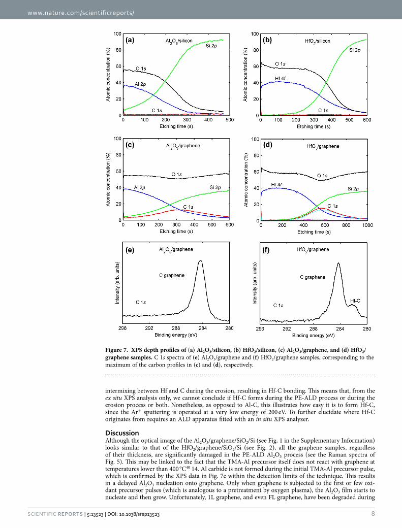
X-ray photoelectron spectroscopy measurements. We carry out ex situ XPS measurements to evaluate the impact of PE-ALD dielectrics on graphene. Four samples are sputtered with an Ar+ gun to perform a depth profile: 5.5-nm-thick Al2O3 and 5.9-nm-thick HfO2 are deposited either on silicon (as references) or on graphene/SiO2/silicon stacks (hereafter referred to as Al2O3/silicon, HfO2/silicon, Al2O3/graphene, and HfO2/graphene, respectively). Core level spectra are recorded from carbon (C 1s), oxygen (O 1s), hafnium (Hf 4f), aluminum (Al 2p), and silicon (Si 2p). The elemental composition of the dielectrics obtained from 20-nm-thick reference layers can be estimated from the ratios of the inte-grated intensities of the XPS spectra: [O/Hf] = 2.15 ± 0.1 and [O/Al] = 1.47 ± 0.05. These results testify to the good quality of the dielectrics. We now focus on the C 1s atomic concentration profile and spectra of each sample. Figure 7a,b illustrate the depth profiles of the Al2O3/silicon and HfO2/silicon samples, respectively. In both cases, a small amount of carbon (2% on average) is found in the profiles (except for a ~15% concentration corresponding to adventitious carbon on top of the dielectric layers). Moreover, a slight increase of the carbon concentration is observed when approaching the interface between the dielectric and silicon, most likely originating from residual contamination on silicon before PE-ALD. Figure 7c,d display the depth profiles of the Al2O3/graphene and HfO2/graphene samples, respectively.
Figure 5. Raman spectra: (a) 3L graphene underlying HfO2 and Al2O3. (b) AB-2L graphene underlying HfO2 and Al2O3. (c) t-2L graphene underlying HfO2 and Al2O3. (d) 1L graphene underlying HfO2 and Al2O3.

www.nature.com/scientificreports/
7Scientific RepoRts | 5:13523 | DOi: 10.1038/srep13523
We can clearly identify the presence of graphene between the dielectric and the SiO2/silicon substrate. Figure 7e,f exhibit the C 1s spectra of the Al2O3/graphene and HfO2/graphene samples at the maximum of the carbon profiles, respectively. The main peak at 284.5 eV in both spectra corresponds to graphene. Strikingly, in contrast to the Al2O3/graphene sample, the HfO2/graphene sample displays an additional peak at 281.5 eV. This peak can be attributed to the formation of the metallic carbide Hf-C. Consequently, the HfO2/graphene profile in Fig. 7d can be fitted by its two components: C in graphene and C in Hf-C. At the interface, the Hf-C concentration reaches 2% of the total composition (see the cyan and magenta profiles in Fig. 7d, corresponding to C in graphene and C in Hf-C, respectively). However, it was reported by Engelhard et al.39 that Ar+ sputtering of ALD HfO2 induces the formation of Hf-C (at an ion-gun energy of 2000 eV), amounting to 1% of the total composition. To ascertain that the observed Hf-C peak is not related to sputtering (the Ar+ gun is operated on purpose at the very low energy of 200 eV in the hope of preventing Hf-C formation), we have performed an additional experiment. A 1L graphene is transferred onto an HfO2/SiO2/Si substrate and next subjected to sputtering in the same conditions as before. In the corresponding C 1 s spectrum, the carbide-related peak occurs as well, most likely due to
Figure 6. Raman spectra of HfO2/graphene for graphene layers with thicknesses of HfO2 (0, 0.5, 1 and 5 nm), (a) 1L, (b) AB-2L, (c) t-2L (t-2L), (d) 3L graphene and (e) all the AD/AG ratios as a function of the HfO2 thickness.
www.nature.com/scientificreports/
8Scientific RepoRts | 5:13523 | DOi: 10.1038/srep13523
intermixing between Hf and C during the erosion, resulting in Hf-C bonding. This means that, from the ex situ XPS analysis only, we cannot conclude if Hf-C forms during the PE-ALD process or during the erosion process or both. Nonetheless, as opposed to Al-C, this illustrates how easy it is to form Hf-C, since the Ar+ sputtering is operated at a very low energy of 200 eV. To further elucidate where Hf-C originates from requires an ALD apparatus fitted with an in situ XPS analyzer.
DiscussionAlthough the optical image of the Al2O3/graphene/SiO2/Si (see Fig. 1 in the Supplementary Information) looks similar to that of the HfO2/graphene/SiO2/Si (see Fig. 2), all the graphene samples, regardless of their thickness, are significantly damaged in the PE-ALD Al2O3 process (see the Raman spectra of Fig. 5). This may be linked to the fact that the TMA-Al precursor itself does not react with graphene at temperatures lower than 400 °C40 14. Al carbide is not formed during the initial TMA-Al precursor pulse, which is confirmed by the XPS data in Fig. 7e within the detection limits of the technique. This results in a delayed Al2O3 nucleation onto graphene. Only when graphene is subjected to the first or few oxi-dant precursor pulses (which is analogous to a pretreatment by oxygen plasma), the Al2O3 film starts to nucleate and then grow. Unfortunately, 1L graphene, and even FL graphene, have been degraded during
Figure 7. XPS depth profiles of (a) Al2O3/silicon, (b) HfO2/silicon, (c) Al2O3/graphene, and (d) HfO2/graphene samples. C 1s spectra of (e) Al2O3/graphene and (f) HfO2/graphene samples, corresponding to the maximum of the carbon profiles in (c) and (d), respectively.

www.nature.com/scientificreports/
9Scientific RepoRts | 5:13523 | DOi: 10.1038/srep13523
the pretreatment. On the contrary, the XPS results have demonstrated that the Hf-C bonds are quite easily formed, whatever the origin of the bonding. We hypothesize that, during the initial TDMA-Hf precursor pulse, a chemical reaction occurs between the Hf atoms and the C atoms constituting graphene to form Hf-C (its formation temperature is 25 °C)39. Hf in Hf-C bonds may act as a uniform and active template for the subsequent HfO2 growth. Subsequently, the coverage of the first HfO2 layer protects the underlying graphene layer from damage during the following deposition cycles. This may also explain why HfO2 rather than Al2O3 can be directly grown on graphene without out-of-plane covalent functional groups, in low-temperature thermal ALD process41,42.
On the other hand, the origin of the inverse dependence of the AD/AG ratio on the number of graphene layers is not clear. It may be due to the interlayer interactions between the HfO2 layer and graphene or a direct consequence of the HfO2 deposition process or both. Previous works about the impact of the graphene thickness on its physical properties suggest that graphene’s rigidity may increase with increas-ing number of layers43. More precisely, when 1L graphene is deposited on top of the SiO2 substrate, it conforms more easily to the surface morphology of the underlying substrate, thereby more prone to deform compared with FL graphene. Oxygen plasma modification of 2L and FL graphene has been studied in the literature. Calculation results44 predict that oxidized 2L graphene, unlike 1L, still retains its intrinsic properties even if the oxygen density is as high as 50%. Electrical experimental results in the work of Felten et al.45 show that only the top layer of 2L graphene is chemically modified, while the bottom layer maintains its structural integrity. Moreover, it was reported that the chemical modification of FL graphene occurs layer by layer46,47. The Raman spectra of HfO2/graphene (blue curves in Fig. 5) show that the AD/AG ratio of 1L graphene is much larger than that of FL graphene and the D’ peak is separated from the G peak in the Raman spectrum of 1L graphene. The formation of Hf-C bonds means a chemical adsorption of Hf atoms on graphene and the conversion of the bond from sp2 to sp3, with a resulting increase of the D peak and separation of the D’ peak. In addition, the oxygen plasma pulse is very aggressive toward 1L graphene48. Besides, the poor rigidity of 1 L graphene results in its fracture and wrinkling49. All these effects would induce damages in the graphene lattice e.g. vacancies, dislocations and dangling bonds. In sharp contrast to 1L, the AD/AG ratios of FL graphene significantly decrease. Hf-C bonds are only present on the top layer due to preferential chemisorption of Hf atoms. Since the plasma pulse is less reactive to FL graphene than 1L50 and graphene becomes more rigid with the number of layers, this may lead to less damage in FL graphene.
The I2D/IG ratio and the FWHM of the 2D peak can be used to easily distinguish 1L and t-2L graphene. More specifically, pristine 1L graphene has a I2D/IG ratio of about 2 and a FWHM of 35 cm−1, while the I2D/IG ratio and the FWHM of t-2L graphene are about 6 and 28 cm−1, respectively51. Our results reveal another interesting behavior: after depositing a 5-nm-thick HfO2 film, t-2L graphene presents “1L-like” features. In other words, when the thickness of the HfO2 film increases from 0 to 5 nm, the I2D/IG ratio reduces from 5.83 to 1.97 and the 2D peak FWHM increases from 26 to 38 cm−1 (see Fig. 6c). It is emphasized here that the I2D/IG ratio of about 2 and the 2D peak FWHM of about 35 cm−1 are the fea-tures of 1L graphene32, while t-2L graphene has a I2D/IG ratio of about 6 and a 2D peak FWHM of about 28 cm−1 (see ref. 51). We suggest that the C atoms in the top layer of t-2L intermixing with Hf atoms and O atoms form an interfacial layer, which is a complex amorphous layer. It is supported by the of the cross-sectional HAADF-STEM image as shown in the insert of Fig. 2c. This is consistent with a previous work52. In Fig. 6c, we can see that the spectrum of t-2L gradually becomes 1L-like upon augmenting the HfO2 thickness. We make the assumption that, below 5 nm, the interfacial layer is not completely formed. In contrast, for 5 nm, the top graphene layer is entirely incorporated into the interfacial layer, leaving a stack made up of HfO2/amorphous interlayer/1L-like graphene. μ RS cannot detect that interfacial layer because it is amorphous. On the other hand, Felten et al.45 observed a similar behavior with AB-2L under different plasma conditions. Indeed, they show by electrical measurements that after long-time and mild plasma treatment, 1L becomes an insulator, while AB-2L graphene still retains its ambipolar property with a relatively high charge mobility. They attribute these facts to the chemically modified top graphene layer and decoupling between the top and bottom layer. However, we did not observe the same behavior for AB-2L and 3L.
As shown in Fig. 6e, the AD/AG ratios of FL graphene decrease with increasing the thickness of HfO2. This is also consistent with the above discussions. More specifically, the increase of the HfO2/graphene thickness makes it more difficult to conform to the surface morphology of the underlying substrate, and as a consequence graphene is less prone to deform.
It is worth emphasizing that FL graphene may be a prospective material with regard to applications such as transistors and sensors. For instance, it has been reported that the sheet resistance of 2L graphene is smaller than that of 1L graphene and the low-frequency 1/f noise in the transistor (30-nm gate length) made from 2L graphene is strongly suppressed compared with 1L graphene transistors53,54.
ConclusionWe have investigated the structural damage in graphene underlying dielectrics (HfO2 and Al2O3) depos-ited by remote PE-ALD. Our results show that FL graphene is less damaged than 1L graphene; the damage level of FL graphene decreases not only with the number of graphene layers but also with the thickness of HfO2. Interestingly, the Raman spectrum of t-2L graphene underlying HfO2 presents the fea-tures of that of as-transferred 1L graphene. XPS measurements indicate that Hf-C is easily formed. After

www.nature.com/scientificreports/
1 0Scientific RepoRts | 5:13523 | DOi: 10.1038/srep13523
coverage by the first HfO2, the bottom graphene layer has an additional protection. The oxygen plasma pulse in PE-ALD is less reactive to FL graphene than 1L. Graphene rigidity increases with the number of graphene layers. Moreover, it also increases with the thickness of HfO2. These may be the reasons of FL graphene less damaged in PE-ALD HfO2. Therefore, FL graphene, more particularly, t-2L graphene allows for controlling/limiting the defect formation during the PE-ALD HfO2 process and might be a prospective material for applications such as graphene-based transistors and sensing devices. It appears that the thickness of PE-ALD HfO2 can be arbitrarily scaled down to 5 nm. Our results open up direct perspectives for FL graphene and HfO2 gate dielectric in graphene-based transistor applications.
MethodsAPCVD graphene conditions. Graphene is synthesized by APCVD with dilute methane (5% in argon) as hydrocarbon precursor on copper foils (Alfa Aesar #13382). The samples are grown at 1000 °C for 1 h under flows of 500 sccm of argon, 20 sccm of hydrogen, and 0.2 sccm of dilute methane. Graphene is then transferred onto 300-nm-thick SiO2/Si substrates (to easily observe graphene with a conventional white light microscope) by the usual method based on PMMA, after etching the copper foil in ammo-nium persulfate.
Process conditions for PE-ALD of dielectrics on graphene. HfO2 and Al2O3 films are deposited on graphene/SiO2/Si stacks, by PE-ALD (Fiji F200 from Ultratech/Cambridge NanoTech Inc., MA) at 250 °C. The plasma source, inductively coupled at 13.56 MHz, is far away from the samples. It is very important to note that the distance between the plasma source and sample location is larger than 40 cm since the type and concentration of the reactive species (electrons, ions, and radicals) strongly depend on this distance. Outside of the glow discharge, only long lifetime radicals are present while ions and electrons recombine quickly.
In order to remove the native stress and polymethyl methacrylate (PMMA) residues from growth and transfer, the graphene samples on the SiO2/Si substrate first are annealed at 250 °C for 2 h in the deposi-tion chamber under pressure of 80 mtorr (argon gas). During both dielectric film depositions, the pulse duration of the oxygen plasma (oxidant precursor) is 10 s for each cycle. The flows of the oxygen plasma and the argon carrier gas are 20 and 200 sccm, respectively. The metallic and oxidant precursor pulses are separated by a short argon purge of 5 s. To obtain uniform dielectric films and avoid graphene etching, the metallic precursors are first pulsed on the graphene surface. The metallic precursors can adsorb or react with carbon to form the related metal oxides following the first oxidant precursor pulse. In con-trast, if the first pulse is a single cycle of oxygen plasma, the graphene surface is possibly damaged or non-uniform dielectric films are formed. The other parameters related to the metallic precursors and the final thickness of both dielectric films are listed in Table 1. The thickness of the dielectric films is meas-ured by in situ ellipsometry from reference films directly deposited on silicon substrates. The composi-tion of the dielectric films is characterized by XPS. In order to investigate the damage level of graphene upon different oxygen plasma power levels, HfO2 and Al2O3 films are deposited on graphene/SiO2/Si stacks with nominal 300 W and with reduced oxygen plasma power of 200 and 150 W, respectively.
Raman spectroscopy system. A LabRam HR 800 confocal laser system from Horiba Jobin Yvon was used for the acquisition of the Raman spectra. The measurements are performed at room temper-ature with a laser wavelength λ = 514 nm in backscattering geometry. The laser beam is focused on the center of hexagons and a 100 × objective (NA = 0.95) is used to collect the signal. The incident power is kept below 1 mW. Low resolution (150 g/mm) and high resolution (1800 g/mm) gratings are used for the measurements.
XPS characterization. A ThermoFisher Scientific K-alpha spectrometer is employed. It is equipped with a monochromatized Al Kα 1,2 x-ray source and a hemispherical deflector analyzer. The spectra are recorded at constant pass energy (150 eV for depth profiling and survey; 30 eV for high resolution spec-tra). A flood gun (low energy electrons and Ar ions) is used during all the measurements. During the sputtering, the Ar+ ion gun is operated at a low energy (200 eV), with an erosion time of 5 s per cycle,
Dielectric Name HfO2 Al2O3
Precursor acronym TDMA-Hf TMA
Precursor chemical formula [(CH3)2N]4Hf Al2(CH3)6
Precursor temperature (°C) 75 25
Precursor pulse duration (s) 0.25 0.06
Cycle number (cycle) 55 55
Final thickness (nm) 5.9 5.5
Table 1. Process conditions in PE-ALD and thicknesses of the two dielectric films.

www.nature.com/scientificreports/
1 1Scientific RepoRts | 5:13523 | DOi: 10.1038/srep13523
and the analysis is done in snapshot mode. The XPS data are treated with the Avantage software. High resolution spectra are fitted by Gaussian-Lorentzian lineshapes with an Avantage “smart” background (i.e. a Shirley background in most cases, or a linear background in case the lineshape decreases with increasing BE).
References1. Avouris, P. Graphene: electronic and photonic properties and devices. Nano Lett. 10, 4285–4294 (2010).2. Novoselov, K. S. et al. A roadmap for graphene. Nature 490, 192–200 (2012).3. Jin, Z., Su, Y., Chen, J., Liu, X. & Wu, D. Study of AlN dielectric film on graphene by Raman microscopy. Appl. Phys. Lett. 95,
233110 (2009).4. Novoselov, K. S. et al. Electric field effect in atomically thin carbon films. Science 306, 666–669 (2004).5. Chen, C.-T., Casu, E. A., Gajek, M. & Raoux, S. Low-damage high-throughput grazing-angle sputter deposition on graphene.
Appl. Phys. Lett. 103, 033109 (2013).6. Ganapathi, K. L., Bhat, N. & Mohan, S. Optimization of HfO2 films for high transconductance back gated graphene transistors.
Appl. Phys. Lett. 103, 073105 (2013).7. Yu, M., Yuan, W., Li, C., Hong, J.-D. & Shi, G. Performance enhancement of a graphene–sulfur composite as a lithium–sulfur
battery electrode by coating with an ultrathin Al2O3 film via atomic layer deposition. J. Mater. Chem. A. 2, 7360 (2014).8. Lee, B. et al. Conformal Al2O3 dielectric layer deposited by atomic layer deposition for graphene-based nanoelectronics. Appl.
Phys. Lett. 92, 203102 (2008).9. Nayfeh, O. M., Marr, T. & Dubey, M. Impact of plasma-assisted atomic-layer-deposited gate dielectric on graphene transistors.
IEEE Electron Device Lett. 32, 473–475 (2011).10. Wu, Y. Q. et al. Top-gated graphene field-effect-transistors formed by decomposition of SiC. Appl. Phys. Lett. 92, 092102 (2008).11. Addou, R., Dahal, A. & Batzill, M. Growth of a two-dimensional dielectric monolayer on quasi-freestanding graphene. Nat.
Nanotechnol. 8, 41–45 (2013).12. Wang, X., Tabakman, S. M. & Dai, H. Atomic layer deposition of metal oxides on as-transferred and functionalized graphene. J.
Am. Chem. Soc. 130, 8152–8153 (2008).13. Wheeler, V. et al. Fluorine functionalization of epitaxial graphene for uniform deposition of thin high-κ dielectrics. Carbon 50,
2307–2314 (2012).14. Jandhyala, S. et al. Atomic layer deposition of dielectrics on graphene using reversibly physisorbed ozone. ACS Nano 6, 2722–2730
(2012).15. Lin, Y.-M. et al. Operation of graphene transistors at gigahertz frequencies. Nano Lett. 9, 422–426 (2009).16. Wang, L. et al. Ultrathin oxide films by atomic layer deposition on graphene. Nano Lett. 12, 3706–3710 (2012).17. Alaboson, J. M. P. et al. Seeding atomic layer deposition of high-k dielectrics on epitaxial graphene with organic self-assembled
monolayers. ACS Nano 5, 5223–5232 (2011).18. Robinson, J. A. et al. Epitaxial graphene materials integration: effects of dielectric overlayers on structural and electronic
properties. ACS Nano 4, 2667–2672 (2010).19. Tselev, A. et al. Near-field microwave microscopy of high-κ oxides grown on graphene with an organic seeding layer. Appl. Phys.
Lett. 103, 243105 (2013).20. Fallahazad, B. et al. Scaling of Al2O3 dielectric for graphene field-effect transistors. Appl. Phys. Lett. 100, 093112 (2012).21. Justice M. P. A. et al. Templating sub-10 nm atomic layer deposited oxide nanostructures on graphene via one-dimensional
organic self-assembled monolayers. Nano Lett. 13, 5763–5770 (2013).22. Shin, W. C., Bong, J. H., Choi, S.-Y. & Cho, B. J. Functionalized graphene as an ultrathin seed layer for the atomic layer deposition
of conformal high-k dielectrics on graphene. ACS Appl. Mater. Interfaces 5, 11515–11519 (2013).23. Dlubak, B. et al. Are Al2O3 and MgO tunnel barriers suitable for spin injection in graphene? Appl. Phys. Lett. 97, 092502 (2010).24. Qiu, X. P. et al. Disorder-free sputtering method on graphene. AIP Adv. 2, 032121 (2012).25. Lee, B. et al. Characteristics of high-k Al2O3 dielectric using ozone-based atomic layer deposition for dual-gated graphene
devices. Appl. Phys. Lett. 97, 043107 (2010).26. Park, S. J. et al. Ultrasensitive flexible graphene based field-effect transistor (FET)-type bioelectronic nose. Nano Lett. 12,
5082–5090 (2012).27. Rao, F. B., Almumen, H., Fan, Z., Li, W. & Dong, L. X. Inter-sheet-effect-inspired graphene sensors: design, fabrication and
characterization. Nanotechnology 23, 105501 (2012).28. Lee, S., Lee, K. & Zhong, Z. Wafer scale homogeneous bilayer graphene films by chemical vapor deposition. Nano Lett. 10,
4702–4707 (2010).29. Reckinger, N., Felten, A., Santos, C. N., Hackens, B. & Colomer, J.-F. The influence of residual oxidizing impurities on the
synthesis of graphene by atmospheric pressure chemical vapor deposition. Carbon 63, 84–91 (2013).30. Wu, B. et al. Equiangular Hexagon-Shape-Controlled Synthesis of Graphene on Copper Surface. Adv. Mater 23, 3522–3525
(2011).31. Wu, B. et al. Self-organized graphene crystal patterns. NPG Asia Mater 5, e36 (2013).32. Ferrari, A. C. & Basko, D. M. Raman spectroscopy as a versatile tool for studying the properties of graphene. Nat. Nanotechnol.
8, 235–246 (2013).33. Huang, M., Yan, H., Heinz, T. F. & Hone, J. Probing strain-induced electronic structure change in graphene by Raman
spectroscopy. Nano Lett. 10, 4074–4079 (2010).34. Casiraghi, C., Pisana, S., Novoselov, K. S., Geim, A. K. & Ferrari, A. C. Raman fingerprint of charged impurities in graphene.
Appl. Phys. Lett. 91, 233108 (2007).35. Kalbac, M. et al. The influence of strong electron and hole doping on the Raman intensity of chemical vapor-deposition graphene.
ACS Nano 4, 6055–6063 (2010).36. Ferrari, A. C. Raman spectroscopy of graphene and graphite: disorder, electron–phonon coupling, doping and nonadiabatic
effects. Solid State Commun. 143, 47–57 (2007).37. Basko, D. M., Piscanec, S. & Ferrari, A. C. Electron-electron interactions and doping dependence of the two-phonon Raman
intensity in graphene. Phys. Rev. B. 80, 165413 (2009).38. Lim, T., Kim, D. & Ju, S. Direct deposition of aluminum oxide gate dielectric on graphene channel using nitrogen plasma
treatment. Appl. Phys. Lett. 103, 013107 (2013).39. Engelhard, M., Herman, J., Wallace, R. & Baer, D. As-received, ozone cleaned and Ar+ sputtered surfaces of hafnium oxide
grown by atomic layer deposition and studied by XPS. Surf. Sci. Spectra 18, 46–57 (2011).40. Pirkle, A., Wallace, R. B. & Colombo, L. In situ studies of Al2O3 and HfO2 dielectrics on graphite. Appl. Phys. Lett. 95, 133106
(2009).

www.nature.com/scientificreports/
1 2Scientific RepoRts | 5:13523 | DOi: 10.1038/srep13523
41. Meric, I. et al. Current saturation in zero-bandgap, top-gated graphene field-effect transistors. Nat. Nanotechnol. 3, 654–659 (2008).
42. Zou, K., Hong, X., Keefer, D. & Zhu, J. Deposition of high-quality HfO2 on graphene and the effect of remote oxide phonon scattering. Phys. Rev. Lett. 105, 126601 (2010).
43. Gupta, A., Chen, G., Joshi, P., Tadigadapa, S. & Eklund, P. C. Raman scattering from high-frequency phonons in supported n-graphene layer films. Nano Lett. 6, 2667–2673 (2006).
44. Nourbakhsh, A. et al. Single layer vs bilayer graphene: a comparative study of the effects of oxygen plasma treatment on their electronic and optical properties. J. Phys. Chem. C. 115, 16619–16624 (2011).
45. Felten, A. et al. Single- and double-sided chemical functionalization of bilayer graphene. Small 9, 631–639 (2013).46. Luo, Z. et al. Thickness-dependent reversible hydrogenation of graphene layers. ACS Nano 3, 1781–1788 (2009).47. Gokus, T. et al. Making graphene luminescent by oxygen plasma treatment. ACS Nano 3, 3963–3968 (2009).48. Ryu, S., Maultzsch, J., Han, M. Y., Kim, P. & Brus, L. E. Raman spectroscopy of lithographically patterned graphene nanoribbons.
ACS Nano 5, 4123–4130 (2011).49. Ni, Z. H. et al. Tunable stress and controlled thickness modification in graphene by annealing. ACS Nano 2, 1033–1039 (2008).50. Jaiswal, M. et al. Controlled hydrogenation of graphene sheets and nanoribbons. ACS Nano 5, 888–896 (2011).51. Fang, W. et al. Rapid identification of stacking orientation in isotopically labeled chemical-vapor grown bilayer graphene by
Raman spectroscopy. Nano Lett. 13, 1541–1548 (2013).52. Zhou, P. et al. Direct deposition of uniform high-k dielectrics on graphene. Sci. Rep. 4, 6448 (2014).53. Lin, Y.-M. & Avouris, P. Strong suppression of electrical noise in bilayer graphene nanodevices. Nano Lett. 8, 2119–2125 (2008).54. Liu, J., Rumyantsev, S., Shur, M. S. & Balandin, A. A. Origin of 1/f noise in graphene multilayers: surface vs. volume. Appl. Phys.
Lett. 102, 093111 (2013).
AcknowledgmentsThe authors thank the staff of UCL’s Winfab and Welcome for technical support. Xiaohui Tang is a senior research of UCL. This work is financially supported by the Multi-Sensor-Platform for Smart Building Management project (No. 611887) and the Action de Recherche Concertée (ARC) “StressTronics”, Communauté française de Belgique. Part of this work is financially supported by the Belgian Fund for Scientific Research (FRS-FNRS) under FRFC contract “Chemographene” (No. 2.4577.11). J.-F. Colomer and B. Hackens are Research Associates of FRS-FNRS. This research used resources of the Electron Microscopy Service located at the University of Namur (“Plateforme Technologique Morphologie – Imagerie”). This research used resources of the ELISE Service of the University of Namur. This Service is member of the “Plateforme Technologique SIAM”. The research leading to this work has received partial funding from the European Union Seventh Framework Program under grant agreement No 604391 Graphene Flagship.
Author ContributionsX.T. designed the experiment and wrote the manuscript. N.R. synthesized graphene, took the SEM pictures, and transferred graphene on SiO2 substrates. X.T. and O.P. performed the PE-ALD. N.R. and X.T. performed the Raman measurements. X.T. and F.U. analyzed the Raman data. N.R. and P.L. performed the XPS and analyzed the results. H.I. and S.T. took the TEM pictures. D.C. provided the AFM images and analysis. J.-F.C., J.-P.R., B.H. and L.F. discussed the results. All authors reviewed the manuscript.
Additional InformationSupplementary information accompanies this paper at http://www.nature.com/srepCompeting financial interests: The authors declare no competing financial interests.How to cite this article: Tang, X. et al. Damage evaluation in graphene underlying atomic layer deposition dielectrics. Sci. Rep. 5, 13523; doi: 10.1038/srep13523 (2015).
This work is licensed under a Creative Commons Attribution 4.0 International License. The images or other third party material in this article are included in the article’s Creative Com-
mons license, unless indicated otherwise in the credit line; if the material is not included under the Creative Commons license, users will need to obtain permission from the license holder to reproduce the material. To view a copy of this license, visit http://creativecommons.org/licenses/by/4.0/