High k dielectrics for future generation memory devices (Invited Paper)
7
High-k dielectrics for future generation memory devices (Invited Paper) J.A. Kittl a, * , K. Opsomer a , M. Popovici a , N. Menou a , B. Kaczer a , X.P. Wang a , C. Adelmann a , M.A. Pawlak a , K. Tomida a , A. Rothschild a , B. Govoreanu a , R. Degraeve a , M. Schaekers a , M. Zahid a , A. Delabie a , J. Meersschaut a , W. Polspoel a , S. Clima a , G. Pourtois a , W. Knaepen b , C. Detavernier b , V.V. Afanas’ev c , T. Blomberg d , D. Pierreux e , J. Swerts e , P. Fischer e , J.W. Maes e , D. Manger f , W. Vandervorst a , T. Conard a , A. Franquet a , P. Favia a , H. Bender a , B. Brijs a , S. Van Elshocht a , M. Jurczak a , J. Van Houdt a , D.J. Wouters a a IMEC, Kapeldreef 75, Leuven 3001, Belgium b Dept. of Solid State Sciences, Universiteit Gent, Krijgslaan 281/s1, 9000 Gent, Belgium c Dept. of Physics and Astronomy, Katholieke Universiteit Leuven, Celestijnenlaan 200D, 3001 Leuven, Belgium d ASM Microchemistry, Väinö Auerin Katu 12 A, 00560 Helsinki, Finland e ASM Belgium, Kapeldreef 75, 3001 Leuven, Belgium f Qimonda, Kapeldreef 75, 3001 Leuven, Belgium article info Article history: Received 3 March 2009 Accepted 5 March 2009 Available online 13 March 2009 Keywords: High-k DRAM Flash SrTiO3 abstract The requirements and development of high-k dielectric films for application in storage cells of future gen- eration flash and Dynamic Random Access Memory (DRAM) devices are reviewed. Dielectrics with k- value in the 9–30 range are studied as insulators between charge storage layers and control gates in flash devices. For this application, large band gaps (>6 eV) and band offsets are required, as well as low trap densities. Materials studied include aluminates and scandates. For DRAM metal–insulator–metal (MIM) capacitors, aggressive scaling of the equivalent oxide thickness (with targets down to 0.3 nm) drives the research towards dielectrics with k-values >50. Due to the high aspect ratio of MIMCap struc- tures, highly conformal deposition techniques are needed, triggering a substantial effort to develop Atomic Layer Deposition (ALD) processes for the deposition of metal gates and high-k dielectrics. Mate- rials studied include Sr- and Ba-based perovskites, with SrTiO 3 as one of the most promising candidates, as well as tantalates, titanates and niobates. Ó 2009 Elsevier B.V. All rights reserved. 1. Introduction Recently, much work has focused on the development of high-k dielectrics and metal gates for high-performance logic Complementary Metal–Oxide–Semiconductor (CMOS) applica- tions [1–6]. At the center of this effort and as motivation, was the need to continue to scale equivalent oxide thickness (EOT) without increase in gate leakage. Production-worthy Hf-based high-k dielectric/metal gate solutions were developed achieving band edge work-functions using either replacement gate flows or gate first flows. For this application, the materials studied had k-values in the 10–30 range, with band gaps typically in the 5.8–9 eV range. At the same time, high-k dielectrics are also of great interest for application in mass storage memory devices. In particular, they are being investigated for applications in storage cells for the two largest commodity memory markets: NAND flash and Dynamic Random Access Memory (DRAM). The requirements and materials studied are different than those for high-perfor- mance logic, and are specific for each application. In both cases, the introduction of high-k dielectrics is driven by scaling. How- ever, the requirements are quite different, leading to different groups of materials targeted for DRAM and flash applications. Fig. 1 shows the trend of band gap as a function of dielectric constant observed for high-k dielectrics in general (data for dielectric films studied in this work, in good agreement with literature reports) [2,3]. Within this trend, the regions of inter- est for next generation DRAM and flash applications are indi- cated. As will be overviewed in the next section, materials with very high permittivity are of interest for DRAM capacitors, in which very low EOT values are targeted. In contrast, rela- tively large band gaps and band offsets are needed for flash applications, resulting on the selection of materials with moder- ate k-values. In this paper, we present an overview of the development of high-k dielectrics for storage cells for application in NAND flash and DRAM metal–insulator–metal capacitors (MIMCaps), with emphasis and examples from work performed at IMEC. 0167-9317/$ - see front matter Ó 2009 Elsevier B.V. All rights reserved. doi:10.1016/j.mee.2009.03.045 * Corresponding author. E-mail address: [email protected] (J.A. Kittl). Microelectronic Engineering 86 (2009) 1789–1795 Contents lists available at ScienceDirect Microelectronic Engineering journal homepage: www.elsevier.com/locate/mee
-
Upload
independent -
Category
Documents
-
view
1 -
download
0
Transcript of High k dielectrics for future generation memory devices (Invited Paper)

Microelectronic Engineering 86 (2009) 1789–1795
Contents lists available at ScienceDirect
Microelectronic Engineering
journal homepage: www.elsevier .com/locate /mee
High-k dielectrics for future generation memory devices (Invited Paper)
J.A. Kittl a,*, K. Opsomer a, M. Popovici a, N. Menou a, B. Kaczer a, X.P. Wang a, C. Adelmann a, M.A. Pawlak a,K. Tomida a, A. Rothschild a, B. Govoreanu a, R. Degraeve a, M. Schaekers a, M. Zahid a, A. Delabie a,J. Meersschaut a, W. Polspoel a, S. Clima a, G. Pourtois a, W. Knaepen b, C. Detavernier b, V.V. Afanas’ev c,T. Blomberg d, D. Pierreux e, J. Swerts e, P. Fischer e, J.W. Maes e, D. Manger f, W. Vandervorst a, T. Conard a,A. Franquet a, P. Favia a, H. Bender a, B. Brijs a, S. Van Elshocht a, M. Jurczak a, J. Van Houdt a, D.J. Wouters a
a IMEC, Kapeldreef 75, Leuven 3001, Belgiumb Dept. of Solid State Sciences, Universiteit Gent, Krijgslaan 281/s1, 9000 Gent, Belgiumc Dept. of Physics and Astronomy, Katholieke Universiteit Leuven, Celestijnenlaan 200D, 3001 Leuven, Belgiumd ASM Microchemistry, Väinö Auerin Katu 12 A, 00560 Helsinki, Finlande ASM Belgium, Kapeldreef 75, 3001 Leuven, Belgiumf Qimonda, Kapeldreef 75, 3001 Leuven, Belgium
a r t i c l e i n f o
Article history:Received 3 March 2009Accepted 5 March 2009Available online 13 March 2009
Keywords:High-kDRAMFlashSrTiO3
0167-9317/$ - see front matter � 2009 Elsevier B.V. Adoi:10.1016/j.mee.2009.03.045
* Corresponding author.E-mail address: [email protected] (J.A. Kittl).
a b s t r a c t
The requirements and development of high-k dielectric films for application in storage cells of future gen-eration flash and Dynamic Random Access Memory (DRAM) devices are reviewed. Dielectrics with k-value in the 9–30 range are studied as insulators between charge storage layers and control gates in flashdevices. For this application, large band gaps (>6 eV) and band offsets are required, as well as low trapdensities. Materials studied include aluminates and scandates. For DRAM metal–insulator–metal(MIM) capacitors, aggressive scaling of the equivalent oxide thickness (with targets down to 0.3 nm)drives the research towards dielectrics with k-values >50. Due to the high aspect ratio of MIMCap struc-tures, highly conformal deposition techniques are needed, triggering a substantial effort to developAtomic Layer Deposition (ALD) processes for the deposition of metal gates and high-k dielectrics. Mate-rials studied include Sr- and Ba-based perovskites, with SrTiO3 as one of the most promising candidates,as well as tantalates, titanates and niobates.
� 2009 Elsevier B.V. All rights reserved.
1. Introduction
Recently, much work has focused on the development ofhigh-k dielectrics and metal gates for high-performance logicComplementary Metal–Oxide–Semiconductor (CMOS) applica-tions [1–6]. At the center of this effort and as motivation, wasthe need to continue to scale equivalent oxide thickness (EOT)without increase in gate leakage. Production-worthy Hf-basedhigh-k dielectric/metal gate solutions were developed achievingband edge work-functions using either replacement gate flowsor gate first flows. For this application, the materials studiedhad k-values in the 10–30 range, with band gaps typically inthe 5.8–9 eV range.
At the same time, high-k dielectrics are also of great interestfor application in mass storage memory devices. In particular,they are being investigated for applications in storage cells forthe two largest commodity memory markets: NAND flash and
ll rights reserved.
Dynamic Random Access Memory (DRAM). The requirementsand materials studied are different than those for high-perfor-mance logic, and are specific for each application. In both cases,the introduction of high-k dielectrics is driven by scaling. How-ever, the requirements are quite different, leading to differentgroups of materials targeted for DRAM and flash applications.Fig. 1 shows the trend of band gap as a function of dielectricconstant observed for high-k dielectrics in general (data fordielectric films studied in this work, in good agreement withliterature reports) [2,3]. Within this trend, the regions of inter-est for next generation DRAM and flash applications are indi-cated. As will be overviewed in the next section, materialswith very high permittivity are of interest for DRAM capacitors,in which very low EOT values are targeted. In contrast, rela-tively large band gaps and band offsets are needed for flashapplications, resulting on the selection of materials with moder-ate k-values.
In this paper, we present an overview of the development ofhigh-k dielectrics for storage cells for application in NAND flashand DRAM metal–insulator–metal capacitors (MIMCaps), withemphasis and examples from work performed at IMEC.
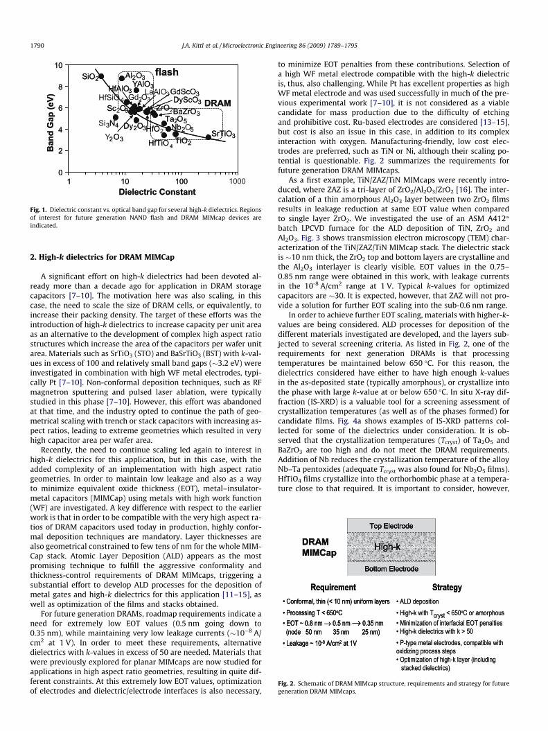
Fig. 2. Schematic of DRAM MIMcap structure, requirements and strategy for futuregeneration DRAM MIMcaps.
0
2
4
6
8
10
1 10 100Dielectric Constant
Ban
d G
ap (e
V)
SiO2 Al2O3
Si3N4SrTiO3TiO2
Nb2O5Ta2O5
HfTiO 4Y2O3
HfO
ZrO2
Gd O3
Dy2O3
BaZrO3Sc2O3
HfAlO3 GdScO3DyScO3
YAlO3
flash
DRAMLaAlO3HfSiO 4
0
2
4
6
8
10
1 10 100 1000Dielectric Constant
Ban
d G
ap (e
V)
SiO2 Al2O3
3N4SrTiO3TiO2
Nb2 5Ta2O5
HfTiO 42O3
HfO2
ZrO2
Dy2O3
BaZrO3Sc O3
HfAlO3 GdScO3DyScO3
YAlO3
flash
DRAM
Fig. 1. Dielectric constant vs. optical band gap for several high-k dielectrics. Regionsof interest for future generation NAND flash and DRAM MIMcap devices areindicated.
1790 J.A. Kittl et al. / Microelectronic Engineering 86 (2009) 1789–1795
2. High-k dielectrics for DRAM MIMCap
A significant effort on high-k dielectrics had been devoted al-ready more than a decade ago for application in DRAM storagecapacitors [7–10]. The motivation here was also scaling, in thiscase, the need to scale the size of DRAM cells, or equivalently, toincrease their packing density. The target of these efforts was theintroduction of high-k dielectrics to increase capacity per unit areaas an alternative to the development of complex high aspect ratiostructures which increase the area of the capacitors per wafer unitarea. Materials such as SrTiO3 (STO) and BaSrTiO3 (BST) with k-val-ues in excess of 100 and relatively small band gaps (�3.2 eV) wereinvestigated in combination with high WF metal electrodes, typi-cally Pt [7–10]. Non-conformal deposition techniques, such as RFmagnetron sputtering and pulsed laser ablation, were typicallystudied in this phase [7–10]. However, this effort was abandonedat that time, and the industry opted to continue the path of geo-metrical scaling with trench or stack capacitors with increasing as-pect ratios, leading to extreme geometries which resulted in veryhigh capacitor area per wafer area.
Recently, the need to continue scaling led again to interest inhigh-k dielectrics for this application, but in this case, with theadded complexity of an implementation with high aspect ratiogeometries. In order to maintain low leakage and also as a wayto minimize equivalent oxide thickness (EOT), metal–insulator-metal capacitors (MIMCap) using metals with high work function(WF) are investigated. A key difference with respect to the earlierwork is that in order to be compatible with the very high aspect ra-tios of DRAM capacitors used today in production, highly confor-mal deposition techniques are mandatory. Layer thicknesses arealso geometrical constrained to few tens of nm for the whole MIM-Cap stack. Atomic Layer Deposition (ALD) appears as the mostpromising technique to fulfill the aggressive conformality andthickness-control requirements of DRAM MIMcaps, triggering asubstantial effort to develop ALD processes for the deposition ofmetal gates and high-k dielectrics for this application [11–15], aswell as optimization of the films and stacks obtained.
For future generation DRAMs, roadmap requirements indicate aneed for extremely low EOT values (0.5 nm going down to0.35 nm), while maintaining very low leakage currents (�10�8 A/cm2 at 1 V). In order to meet these requirements, alternativedielectrics with k-values in excess of 50 are needed. Materials thatwere previously explored for planar MIMcaps are now studied forapplications in high aspect ratio geometries, resulting in quite dif-ferent constraints. At this extremely low EOT values, optimizationof electrodes and dielectric/electrode interfaces is also necessary,
to minimize EOT penalties from these contributions. Selection ofa high WF metal electrode compatible with the high-k dielectricis, thus, also challenging. While Pt has excellent properties as highWF metal electrode and was used successfully in much of the pre-vious experimental work [7–10], it is not considered as a viablecandidate for mass production due to the difficulty of etchingand prohibitive cost. Ru-based electrodes are considered [13–15],but cost is also an issue in this case, in addition to its complexinteraction with oxygen. Manufacturing-friendly, low cost elec-trodes are preferred, such as TiN or Ni, although their scaling po-tential is questionable. Fig. 2 summarizes the requirements forfuture generation DRAM MIMcaps.
As a first example, TiN/ZAZ/TiN MIMcaps were recently intro-duced, where ZAZ is a tri-layer of ZrO2/Al2O3/ZrO2 [16]. The inter-calation of a thin amorphous Al2O3 layer between two ZrO2 filmsresults in leakage reduction at same EOT value when comparedto single layer ZrO2. We investigated the use of an ASM A412TM
batch LPCVD furnace for the ALD deposition of TiN, ZrO2 andAl2O3. Fig. 3 shows transmission electron microscopy (TEM) char-acterization of the TiN/ZAZ/TiN MIMcap stack. The dielectric stackis �10 nm thick, the ZrO2 top and bottom layers are crystalline andthe Al2O3 interlayer is clearly visible. EOT values in the 0.75–0.85 nm range were obtained in this work, with leakage currentsin the 10-8 A/cm2 range at 1 V. Typical k-values for optimizedcapacitors are �30. It is expected, however, that ZAZ will not pro-vide a solution for further EOT scaling into the sub-0.6 nm range.
In order to achieve further EOT scaling, materials with higher-k-values are being considered. ALD processes for deposition of thedifferent materials investigated are developed, and the layers sub-jected to several screening criteria. As listed in Fig. 2, one of therequirements for next generation DRAMs is that processingtemperatures be maintained below 650 �C. For this reason, thedielectrics considered have either to have high enough k-valuesin the as-deposited state (typically amorphous), or crystallize intothe phase with large k-value at or below 650 �C. In situ X-ray dif-fraction (IS-XRD) is a valuable tool for a screening assessment ofcrystallization temperatures (as well as of the phases formed) forcandidate films. Fig. 4a shows examples of IS-XRD patterns col-lected for some of the dielectrics under consideration. It is ob-served that the crystallization temperatures (Tcryst) of Ta2O5 andBaZrO3 are too high and do not meet the DRAM requirements.Addition of Nb reduces the crystallization temperature of the alloyNb–Ta pentoxides (adequate Tcryst was also found for Nb2O5 films).HfTiO4 films crystallize into the orthorhombic phase at a tempera-ture close to that required. It is important to consider, however,

Fig. 3. (a) High resolution TEM image and (b) HAADF-STEM (Z-contrast) analysis of ZAZ stack. TiN, Al2O3 and ZrO2 layers were deposited by ALD. TiN and ZrO2 layers arecrystalline.
J.A. Kittl et al. / Microelectronic Engineering 86 (2009) 1789–1795 1791
that the crystallization temperature (and the phases formed) ofthin films may depend on the substrate, capping layers, composi-tion, contaminants, anneal ambient and film thickness. IS-XRDstudies are, thus, conducted for a variety of conditions to extractthese dependences. Fig. 4b illustrates the anneal temperaturesneeded for several high-k dielectrics and their k-values. This typeof analysis serves as initial screening criteria.
While HfTiO4 or (Nb–Ta)2O5 films may provide intermediatesolutions (e.g. leakage currents down to the 10�7 A/cm2 range wereobtained at 1 V with single layer HfTiO4 films at EOT �0.8 nm), it isunlikely that they can be scaled with low leakage to EOT values be-low 0.5 nm. From the different materials studied in this work, oneof the most promising is SrTiO3. For this reason, but also as modelsystem exemplifying the methods and techniques used for theother systems as well, we go into more details for this system.
Bi-Ta-O
BaTiO3
SrTiO3
BaZrO3
SrTaO3
TiO2 (Rutile) Nb2O5
Ta2O5
HfTiO4
Anneal Temperature (
Bi-Ta-O
BaTiO3
SrTiO3
BaZrO3
SrTaO3
TiO2 (Rutile) Nb2O5
Ta2O5
HfTiO4
200 400 600 800 1000Anneal Temperature (oC)
1000
100
10Die
lect
ric C
onst
ant
Ta2O5
Temperature (oC)100 300 500 700 900
20
35
26
38
(Nb-Ta)2O5
BaZrO3
Two
Thet
a (d
eg) 20
35
25
40
a
b
HfTiO4
Fig. 4. (a) IS-XRD patterns (0.2 �C/s ramp in N2) showing the crystallization ofseveral oxide thin films. Crystallization temperatures for BaZrO3 and Ta2O5 are toohigh for the requirements of future generation DRAMs. (b) Dielectric constants vs.required anneal temperatures for several high-k dielectrics, shaded area corre-sponds to region of interest for future DRAM MIMcaps. For all films, except Bi–Ta–O,the anneal temperatures correspond to those needed for crystallization.
Recently, ALD STO using Sr(thd)2 as Sr-precursor was reportedwith promising results on noble like metal electrodes such as Ruand Pt [13–15]. However, these processes required either highdeposition temperatures (>350 �C) and/or post-deposition annealsin oxidizing ambients, making STO incompatible with manufactur-ing-friendly, lower cost electrodes such as TiN. An alternative pre-cursor set using Sr(t-Bu3Cp)2 was also reported [11,12] for STOgrowth. We further explored this alternative precursor systemfor the growth of STO films for DRAM MIMcap applications [17].
The STO layers were deposited by ALD in a cross-flow ASM Pul-sar� 2000 reactor, at reactor temperatures in the 250–300 �C range,using Sr(t-Bu3Cp)2, H2O, and Ti(OCH3)4. By changing the Sr-precur-sor and the Ti-precursor pulse sequence (Fig. 5), ALD allows thegrowth of a wide compositional variety of STO films from pureTiO2 to Sr-rich STO, with straight forward composition tuning. Thisis typical for well behaved ALD processes. In ALD, the film growthis determined by self-limiting surface reactions, guaranteeing con-formal deposition (Fig. 5 inset) in high aspect ratio structures.
The crystallization behavior of STO films was also studied by IS-XRD [17]. Fig. 6 shows the IS-XRD patterns of STO films on TiN forthree different Sr–Ti compositions, corresponding to Sr/(Sr + Ti)atomic ratios of 0.43 (‘‘Ti-rich”), 0.57 (‘‘Std. Comp.”) and 0.64(‘‘Sr-rich”). The crystallization temperature increases as the com-
Sr(tBu3Cp)2
N2 carrier gas
H2O Ti(OCH3)4 H2O
x* Full cycle
Sr(tBu3Cp)2
N2 carrier gas
H2O Ti(OCH3)4 H2O
x* Full cycle
N2 carrier gas
H2O Ti(OCH3)4 H2O
x* Full cycle
n*Sr-cycle m*Ti-cycle
400 nm
0 0.2 0.4 0.6 0.8 1.0Sr/(Sr+Ti) cycle ratio (n/(n+m))
0.70.60.50.40.30.20.10.0Sr
/(Sr+
Ti) a
tom
ic ra
tio
a
b
Fig. 5. (a) Schematic of low temperature ALD SrTiO3 deposition process and (b) Sr/(Sr + Ti) atomic ratio vs. pulse ratio showing good Sr–Ti composition control for awide range of compositions. Films have excellent conformality (inset in b).

100 300 500 700 900Temperature (oC)
30
35
40
45
30
35
40
45
30
35
40
45
Two
Thet
a (d
eg.)
Std.Comp.
Ti-rich
Sr-rich
TiNTiN
TiNTiN
TiNTiN
TiNTiN
TiNTiN
TiNTiN
(110) SrTiO(110) SrTiO33
(111) SrTiO(111) SrTiO33
(110) SrTiO(110) SrTiO33
(111) SrTiO(111) SrTiO33
(110) SrTiO(110) SrTiO33
(111) SrTiO(111) SrTiO33
Fig. 6. IS-XRD patterns of SrxTiyO3 films on TiN, for three different compositions,showing crystallization into the perovskite phase.
1.E-08
1.E-07
1.E-06
1.E-05
1.E-04
1.E-03
1.E-02
1.E-01
1.E+00
Ti-rich, 600°C
Sr-rich, 550°C EOT=0.49 nm
Std. Comp., 550°C EOT=0.69 nm
100
10-1
10-2
10-3
10-4
10-5
10-6
10-7
10-8
SrTiO3/ALD TiN
1.E-08
1.E-07
1.E-06
1.E-05
1.E-04
1.E-03
1.E-02
1.E-01
1.E+00
Ti-rich, 600°C
Sr-rich, 550°C EOT=0.49 nm
Std. Comp., 550°C EOT=0.69 nm
100
10-1
10-2
10-3
10-4
10-5
10-6
10-7
10-8
SrTiO3/ALD TiN
Jg(A
/cm
2 )
b
Applied Voltage (V)0 0.5 1.0 1.5 2.0
012345678
SrTiO3 (Std. Comp.)
K ~ 20(amorph.)
K ~ 150 (cryst.)
TiNas dep.TiN 500 oCTiN 550 oCTiN 600 oCRu 600 oCPt 650oC
EOT
(nm
)
a
0 10 20 30 40 Thickness (nm)
Fig. 7. (a) EOT vs. thickness plots of ALD SrxTiyO3 films on TiN, Ru and Pt bottomelectrodes (Pt-dot capacitors), for as-deposited STO films and STO films thatreceived post-deposition anneals at 500, 550, 600 and 650 �C; (b) I–V curves (e-injection from TiN) of crystallized ALD SrxTiyO3 thin films on ALD TiN.
1792 J.A. Kittl et al. / Microelectronic Engineering 86 (2009) 1789–1795
position further deviates from that of stoichiometric SrTiO3. Never-theless, all films crystallize below 600 �C. A kink in the pattern isclearly noticeable for the Sr-rich film, indicating a change of latticeparameter at high temperatures. The high temperature latticeparameter for all films is similar and corresponds to that of bulkSrTiO3. The distortion of the lattice parameter at low temperaturesfor Sr-rich films suggests that a metastable structure may be ini-tially formed upon crystallization, likely with incorporation of ex-cess Sr into the STO grains, resulting in the expansion of the latticeparameter. At high temperatures, excess Sr may be released orredistributed, resulting in the shift towards bulk STO values. XRDpatterns did not reveal the formation of Ruddlesden–Popperphases [18] with ordering of excess SrO planes.
Electrical evaluation shows the dramatic change in properties ofthe STO films upon crystallization. Fig. 7a shows the EOT vs. thick-ness plots for ‘‘Std. Comp.” STO films (extracted using Pt-dot capac-itors), comparing as-deposited films to films that received a post-deposition anneal in N2 (1 min) at 500, 550, 600 and 650 �C. Theas-deposited films and films with 500 �C anneal have k-values of�20. This corresponds to amorphous STO. Films that received an-neals at 550 �C and higher temperatures crystallized into theperovskite structure achieving k �150. The k-values indicated cor-respond to those extracted from the slope of the EOT vs. thicknessplots. As observed in Fig. 7a, extrapolations to 0 physical thicknesstypically correspond to non-zero EOT values, in this case, �0.3–0.4 nm. This may be attributed in part to interfacial layers betweenthe electrodes and the dielectric. However, even for ideal inter-faces, an EOT penalty (‘‘dead layer”) is expected, with local reduc-tion of the k-value in the interface region [19]. As a consequence,effective k-values (obtained by simply dividing EOT by physicalthickness) are typically smaller than those obtained from the slopeof EOT vs. thickness plots, and decrease as the film thickness de-creases. Since the roadmap for future DRAM nodes calls for aggres-sive EOT scaling (0.5–0.35 nm), interfacial penalties will becomedominant and need to be minimized. Thus, selection of the elec-trode and optimization of the interface between electrode andhigh-k becomes crucial.
Leakage characterization of the STO films showed a strongdependence on composition, with lower leakage observed for7 nm Sr-rich films compared to 9–12 nm films with higher Ti con-tent (Fig. 7b) [17]. Film thicknesses were extracted by TEM analy-
sis, which also showed the Sr-rich and Std. Comp. films to becrystalline after the 550 �C anneal. The k-values of the crystallineSTO films also depend on composition, with the highest value ob-tained for stoichiometric films (k �220) and k�75 obtained for Sr-rich films (Sr/(Sr + Ti) atomic ratio of 0.64).
The temperature and voltage dependence of the leakage of Sr-rich films was characterized for films with several different thick-nesses. The conduction mechanism was identified as electronichopping between interacting trap sites [20]. In combination withphotoconductivity measurements, the data is consistent with aband gap of 3.25 eV and a band of interacting trap sites at �0.7–1.2 V below the conduction band edge. This was further supportedby ab initio simulations using the local density approximation [20].
Macroscopic leakage measurements were also complementedby conductive atomic-force-microscope (CAFM) analysis, whichshowed conductance through the bulk of STO grains for Sr-richfilms, in contrast to Ti-rich films which exhibited localized high-conductance paths [17].
3. High-k dielectrics for flash applications
Significant effort is currently also dedicated to the study anddevelopment of high-k dielectrics and metal gates for non-volatilememory (NVM) applications [21,22]. Within the commodity mem-ories, the NAND flash market has expanded significantly in recentyears driven by applications in portable devices. One of the reasonsfor the success of NAND flash is its density integration potential,which allows fabrication of large memory arrays.
NAND flash memories currently in the market use floating gate(FG) architectures. The wordline, typically implemented using n+-polycrystalline-Si (poly-Si), runs over several floating gates. Siliconoxide–nitride–oxide (‘‘ONO”) stacks are used as inter- poly-Si

J.A. Kittl et al. / Microelectronic Engineering 86 (2009) 1789–1795 1793
dielectric (IPD) [23], i.e. between the storage FG and the top controlgate (CG). In the present implementation, the poly-Si CG wrapsaround the FG. The sidewall overlap contributes to the capacitancebetween the CG and the FG, which provides the necessary electri-cal coupling for operating the device. External voltages applied onthe top gate (CG) induce a voltage drop over the tunnel dielectric,i.e. between the FG and the Si substrate, which allow carrier trans-port through the tunnel dielectric (program/erase) or just enoughbias for sensing the charge stored on the FG (read out). Reductionof the feature size below 40 nm may, however, requires modifica-tions of the FG cell architecture, due to lack of physical space be-tween neighboring cells, which no longer allows wrapping of theCG over the FG. The resulting structures will be ‘‘planarized” andthe loss of the coupling capacitance from the sidewalls leads tothe degradation of the coupling factor. To address this problem,high-k dielectrics are being studied as candidates to replace ONOstacks as IPD in order to increase the gate coupling factor. In addi-tion to FG architectures, significant work has been recently de-voted to the development of charge trap (CT) flash cells. In thisconcept, the charge is stored in a ‘‘trapping layer” with a high den-sity of deep traps, typically a nitride. High-k dielectrics are alsostudied for CT devices, as blocking oxides (BO) between the traplayer and the control gate. As examples, cross-sections of stacksbeing studied for FG and for CT devices are shown in Fig. 8.
For both for applications, i.e. as IPD in FG or BO in CT devices,dielectrics with large band gaps and band offsets are needed,which practically limits the k-value of the materials to a moderaterange (typically 9–20), as shown in Fig. 1. Typical charge retentionspecs for flash devices require IPD (or BO) with very low leakage.As a consequence, another important consideration for high-kdielectrics targeted for flash devices is to have very low trapdensities.
Al2O3, with a k-value of �9, has been studied as one of the maincandidates to replace ONO as IPD in FG devices or as BO for chargetrap memories [21,22]. Significantly improved device characteris-tics are obtained for crystalline Al2O3 compared to amorphousAl2O3. Upon crystallization, the band gap and band offsets ofAl2O3 increase dramatically [4]. IS-XRD analysis of thin (12–20 nm) Al2O3 films indicates crystallization into the c-Al2O3 phasetypically at �850 �C. However, the crystallization of the films (andconsequently device characteristics, such as retention), texture andmicrostructure were found to be strongly dependent on the depo-sition technique and parameters. Fig. 8a shows a TEM cross-sectionof the top portion of a FG device using Al2O3 as IPD and a TiN metal
Si3N4
D
TaN
(100) S
b)
Poly-Si
Poly-Si
TiN
Al2O3
a)
5 nm
Fig. 8. TEM cross-sections of (a) top portion of a FG device using Al2O3 IPD and TiN CG,TaN CG; (c) schematic of flash cell (charge storage layer is a nitride in CT devices and p
CG. The Al2O3 film in this case has crystallized into the c-phase,with (111) texture, as confirmed by plan view TEM and XRD anal-ysis, and exhibits good retention.
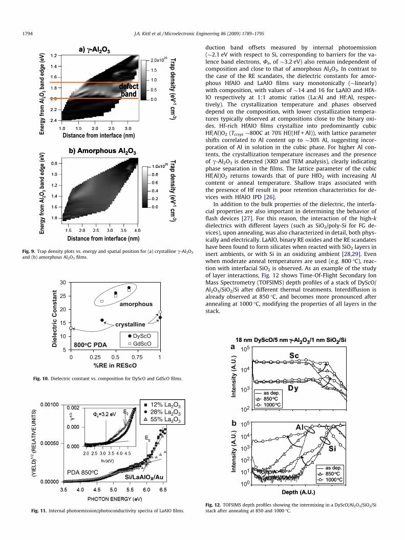
As already mentioned, the density and position of traps in theIPD or BO dielectric have a crucial impact on the device retentionproperties. A new and powerful method for characterizing defectbands in dielectric materials, Trap Spectroscopy by Charge Injec-tion and Sensing (TSCIS), was recently proposed [24]. This tech-nique is quantitative and spectroscopic resulting in a trap densityplot vs. energy and spatial position. Fig. 9 shows the trap densityplots obtained by TSCIS, comparing amorphous to c-Al2O3 [24].For the crystalline c-Al2O3, the defects are localized in a horizontalband between 1.7 and 2.0 eV below the conduction band edge. Incontrast, the trap density spectrum of amorphous Al2O3 showsno distinct features. In the scanned range, traps are distributedevenly in both space and energy (including a significant densityof shallow traps). In combination with the change in band gapand band offsets with crystallization, these observations explainthe significant improvement in retention behavior with crystalliza-tion of the Al2O3.
While, as initial implementation, Al2O3 may be adequate,materials with higher-k are required for future generations. Forthis reason, several dielectrics with k-value in the 12–30 rangeare being investigated. Ideally, the increase in k-value should beaccomplished without a large penalty in band gap (band offset)reduction or trap density increase. Aluminates and scandates ap-pear as candidates that may fulfill these requirements (Fig. 1). Asexample, considering the rare earth (RE) scandates (e.g. DyScOand GdScO), it is possible to increase considerably the k-valuecompared to that of Sc2O3 or the corresponding rare earth binaryoxide (Fig. 10) [25], without a penalty in band gap or band offsets,which remain close to those of Sc2O3 (band gap �6 eV and con-duction band offset respect to Si of �2.0 eV) for a wide composi-tional range. It is interesting to notice, that the RE scandates withk-values >20 shown in Fig. 10 (post-deposition anneal (PDA) of800 �C) are amorphous, while the binary oxides, with lower k-val-ues, are crystalline.
Considering the aluminates such as HfAlO or REAlO, we notethat their crystallization is also delayed with respect to that ofthe binary oxides by the addition of alloying elements. The bandgaps (Eg) obtained for the amorphous aluminates (HfAlO or LaA-lO), of �6 eV, while close to that of amorphous Al2O3 and main-tained for a wide compositional range (see example in Fig. 11),are considerably lower than that of crystalline Al2O3. The con-
SiO2
Al2O3
yScO
i 5 nm Si tunnel oxide
charge storage
Control Gate
BlockingOxide
(high-k)
c)
and (b) CT device with SiO2 tunnel oxide, Si3N4 trapping layer, DyScO/Al2O3 BO andoly-Si in FG devices.)
5
10
15
20
25
30
Die
lect
ric C
onst
ant
DyScOGdScO800oC PDA
amorphous
crystalline
%RE in REScO0 0.25 0.5 0.75 1
Fig. 10. Dielectric constant vs. composition for DyScO and GdScO films.
Fig. 11. Internal photoemission/photoconductivity spectra of LaAlO films.
defectband
b) Amorphous Al2O3
23
a) γ-Al2O3
defectband
b) Amorphous Al2O3
Trap density (eV-1cm
-3)
Distance from interface (nm)
Distance from interface (nm)
Ener
gy fr
om A
l 2O3
band
edge
(eV)
a) γ-Al2O3
Trap density (eV-1cm
-3)
Ener
gy fr
om A
l 2O3
band
edge
(eV)
Fig. 9. Trap density plots vs. energy and spatial position for (a) crystalline c-Al2O3
and (b) amorphous Al2O3 films.
1794 J.A. Kittl et al. / Microelectronic Engineering 86 (2009) 1789–1795
duction band offsets measured by internal photoemission(�2.1 eV with respect to Si, corresponding to barriers for the va-lence band electrons, Ue, of �3.2 eV) also remain independent ofcomposition and close to that of amorphous Al2O3. In contrast tothe case of the RE scandates, the dielectric constants for amor-phous HfAlO and LaAlO films vary monotonically (�linearly)with composition, with values of �14 and 16 for LaAlO and HfA-lO respectively at 1:1 atomic ratios (La:Al and Hf:Al, respec-tively). The crystallization temperature and phases observeddepend on the composition, with lower crystallization tempera-tures typically observed at compositions close to the binary oxi-des. Hf-rich HfAlO films crystallize into predominantly cubicHf(Al)O2 (Tcrsyt �800C at 70% Hf/(Hf + Al)), with lattice parametershifts correlated to Al content up to �30% Al, suggesting incor-poration of Al in solution in the cubic phase. For higher Al con-tents, the crystallization temperature increases and the presenceof c-Al2O3 is detected (XRD and TEM analysis), clearly indicatingphase separation in the films. The lattice parameter of the cubicHf(Al)O2 returns towards that of pure HfO2 with increasing Alcontent or anneal temperature. Shallow traps associated withthe presence of Hf result in poor retention characteristics for de-vices with HfAlO IPD [26].
In addition to the bulk properties of the dielectric, the interfa-cial properties are also important in determining the behavior offlash devices [27]. For this reason, the interaction of the high-kdielectrics with different layers (such as SiO2/poly-Si for FG de-vices), upon annealing, was also characterized in detail, both phys-ically and electrically. LaAlO, binary RE oxides and the RE scandateshave been found to form silicates when reacted with SiO2 layers ininert ambients, or with Si in an oxidizing ambient [28,29]. Evenwhen moderate anneal temperatures are used (e.g. 800 �C), reac-tion with interfacial SiO2 is observed. As an example of the studyof layer interactions, Fig. 12 shows Time-Of-Flight Secondary IonMass Spectrometry (TOFSIMS) depth profiles of a stack of DyScO/Al2O3/SiO2/Si after different thermal treatments. Interdiffusion isalready observed at 850 �C, and becomes more pronounced afterannealing at 1000 �C, modifying the properties of all layers in thestack.
18 nm DyScO/5 nm γγ-Al2O3/1 nm SiO2/Si
1.E+02
1.E+03
1.E+04
1.E+05
0 5000 10000 15000 20000 25000 30000 35000
Depth (A.U.)
Sc
Dyas dep.850oC1000oC
a
1.E+00
1.E+01
1.E+02
1.E+03
1.E+04
1.E+05
0 5000 10000 15000 20000 25000 30000 35000Depth (A.U.)
105
104
103
102
101
100
Si
Al
as dep.850oC1000oC
b
105
104
103
102
18 nm DyScO/5 nm γ-Al2O3/1 nm SiO2/Si
1.E+02
1.E+03
1.E+04
1.E+05
0 5000 10000 15000 20000 25000 30000 35000
Depth (A.U.)
Sc
Dy
Inte
nsity
(A.U
.)
as dep.850oC1000oC
1.E+00
1.E+01
1.E+02
1.E+03
1.E+04
1.E+05
0 5000 10000 15000 20000 25000 30000 35000
105
104
103
102
101
100
Si
Al
Inte
nsity
(A.U
.)
as dep.850oC1000oC
105
104
103
102
Depth (A.U.)
Fig. 12. TOFSIMS depth profiles showing the intermixing in a DyScO/Al2O3/SiO2/Sistack after annealing at 850 and 1000 �C.
J.A. Kittl et al. / Microelectronic Engineering 86 (2009) 1789–1795 1795
4. Summary
An overview of requirements and development work on high-kdielectrics for applications in flash cells and DRAM MIMCaps waspresented, highlighting the main challenges faced. For DRAM MIM-Caps, EOT scaling towards 0.3 nm requires dielectrics with k-values>50, while processing temperatures need to remain <650 �C. Theseconditions are used as first screening criteria. Due to the high as-pect ratio of the DRAM MIMCaps, highly conformal ALD techniquesare studied for film growth. SrTiO3 appears as one of the mostpromising candidates, while HfTiO4 and (Nb–Ta)2O5 may provideintermediate solutions. Dielectrics with k-values in the 9–30 rangeare investigated for flash applications as IPD in FG memories or BOin CT memories. For flash, achieving adequate band offsets as wellas low trap densities are key criteria for selection of the dielectric.Al2O3 was presented as reference material, as well as examplesfrom the evaluation of aluminates and rare earth scandates.
References
[1] G.D. Wilk, R.M. Wallace, J.M. Anthony, J. Appl. Phys. 89 (2001) 5243.[2] J. Robertson, Eur. J. Appl. Phys. 28 (2004) 265.[3] D.G. Schlom, J.H. Haeni, MRS Bull. 2002 (2002) 198 (March).[4] V.V. Afanas’ev, A. Stesmans, J. Appl. Phys. 102 (2007) 081301.[5] M. Houssa, L. Pantisano, L.A. Ragnarsson, R. Degraeve, T. Schram, G. Pourtois, S.
De Gendt, G. Groeseneken, M. Heyns, Mater. Sci. Eng. R 51 (2006) 37.[6] M.R. Visokay, J.J. Chambers, A.L.P. Rotondaro, A. Shanware, L. Colombo, Appl.
Phys. Lett. 80 (2002) 3183.[7] D. Roy, S.B. Krupanidhi, Appl. Phys. Lett. 62 (1993) 1056.[8] C.S. Hwang, S.O. Park, C.S. Kang, H.J. Cho, H.K. Kang, S.T. Ahn, M.Y. Lee, Jpn. J.
Appl. Phys. 34 (1995) 5178.[9] C.S. Hwang, Mater. Sci. Eng. B 56 (1998) 178.
[10] C.S. Hwang, S. Park, H.J. Cho, C.S. Kang, H.K. Kang, S.I. Lee, M.Y. Lee, Appl. Phys.Lett. 67 (1995) 2819.
[11] M. Vehkamäki, T. Hatanpää, T. Hänninen, M. Ritala, M. Leskelä, Electrochem.Solid-State Lett. 2 (1999) 504.
[12] M. Vehkamäki, T. Hänninen, M. Ritala, M. Leskelä, T. Sajavaara, E. Rauhalaand,J. Keinonen, Chem. Vapor Depos. 7 (2001) 75.
[13] J.-H. Ahn, J.-Y. Kim, S.-W. Kang, J.-H. Kim, J.-S. Roh, Appl. Phys. Lett. 91 (2007)062910.
[14] O.S. Kwon, S.W. Lee, J.H. Han, C.S. Hwang, J. Electrochem. Soc. 154 (6) (2007)G127.
[15] S.W. Lee, O.S. Kwon, J.H. Han, C.S. Hwang, Appl. Phys. Lett. 92 (2008) 222903.[16] D.-S. Kil, H.-S. Song, K.-J. Lee, K. Hong, J.-H. Kim, K.-S. Park, S.-J. Yeom, J.-S. Roh,
N.-J. Kwak, H.-C. Sohn, J.-W. Kim, S.-W. Park, Symp. VLSI Tech. Dig. 2006 (2006)38.
[17] N. Menou, X.P. Wang, B. Kaczer, W. Polspoel, M. Popovici, K. Opsomer, M.A.Pawlak, W. Knaepen, C. Detavernier, T. Blomberg, D. Pierreux, J. Swerts, J.W.Maes, P. Favia, H. Bender, B. Brijs, W. Vandervorst, S. Van Elshocht, D.J.Wouters, S. Biesemans, J.A. Kittl, IEDM Tech. Dig. 2008 (2008) 929.
[18] S.N. Ruddlesden, P. Popper, Acta Crystallogr. 10 (1957) 538.[19] M. Stengel, N.A. Spaldin, Nature 443 (2006) 679.[20] D. Manger, B. Kaczer, N. Menou, S. Clima, D.J. Wouters, V.V. Afanas’ev, J.A. Kittl,
Microelectron. Eng. 86 (2009) 1815.[21] C.H. Lee, S.H. Hur, Y.C. Shin, J.H. Choi, D.G. Park, K. Kim, Appl. Phys. Lett. 86
(2005) 152908.[22] C.H. Lee, K.I. Choi, M.K. Cho, Y.H. Song, K.C. Park, K. Kim, IEDM Tech. Dig. 2003
(2003) 613.[23] S. Mori, Y.Y. Araki, M. Sato, H. Meguro, H. Tsunoda, E. Kamiya, K. Yoshikawa, N.
Arai, E. Sakagami, IEEE Trans. Electron Dev. 43 (1996) 47.[24] R. Degraeve, M.J. Cho, B. Govoreanu, B. Kaczer, M. Zahid, J. Van Houdt, M.
Jurczak, IEDM Tech. Dig. 2008 (2008) 775.[25] C. Zhao, T. Witters, B. Brijs, H. Bender, O. Richard, M. Caymax, T. Heeg, J.
Schubert, V.V. Afanas’ev, A. Stesmans, D.G. Schlom, Appl. Phys. Lett. 86 (2005)132903.
[26] B. Govoreanu, R. Degraeve, M. Zahid, L. Nyns, M. Cho, B. Kaczer, M. Jurczak, J.A.Kittl, J. Van Houdt, Microelectron. Eng. 86 (2009) 1807.
[27] B. Govoreanu, D. Wellekens, L. Haspeslagh, D.P. Brunco, J. De Vos, D. RuizAguado, P. Blomme, K. van der Zanden, J. Van Houdt, Solid-State Electron. 52(2008) 557.
[28] C. Adelmann, S. Van Elshocht, A. Franquet, T. Conard, O. Richard, H. Bender, P.Lehnen, S. De Gendt, Appl. Phys. Lett. 92 (2008) 112902.
[29] S. Van Elshocht, C. Adelmann, T. Conard, A. Delabie, A. Franquet, L. Nyns, O.Richard, P. Lehnen, J. Swerts, S. De Gendt, J. Vac. Sci. Technol. A 26 (2008) 724.