Effects of Cu, Bi, and In on microstructure and tensile properties of Sn-Ag-X(Cu, Bi, In) solders
8
Effects of Cu, Bi, and In on Microstructure and Tensile Properties of Sn-Ag-X(Cu, Bi, In) Solders M.L. HUANG and L. WANG Effects of minor additions of Cu, Bi, and In on microstructure, melting temperature, and tensile properties of Sn-Ag–based lead-free solders were investigated. It was found that the intermetallic compounds (IMCs) Ag 2 In and Cu 6 Sn 5 are formed in In- and Cu-containing solders, respectively. At low concen- tration, Bi dissolved in the Sn matrix and tended to precipitate pure Bi particles at the solubility limit of 4 wt pct Bi. The formation of large Ag 3 Sn precipitates from the solder matrix was suppressed when alloying bismuth into the Sn-Ag alloy. The Bi addition resulted in a significant linear increase of the ultimate tensile strength (UTS) of solders, which is attributed to a solid-solution hardening mechanism. Solder strengthening due to In and Cu is less pronounced and attributed to a dispersion strengthening mechanism. The additions of Cu, Bi, and In all depressed the melting temperatures of Sn-Ag–based solders; however, In is the most effective one. I. INTRODUCTION DUE to the environmental and health concerns, traditional tin-lead solders used in electronic packaging will be com- pletely replaced by lead-free solders in the near future. Among the various alloy systems, Sn-Ag solder is one of the earliest commercially available lead-free solders and also the most attractive candidate for electronic packaging, which provides better mechanical properties than those of the eutectic Sn- 37Pb solder. [1,2] However, the high melting temperature of Sn-3.5Ag (221 °C) has confined its application in electronic packaging, since current manufacturing technologies are based upon the eutectic temperature of Sn-Pb (183 °C). It is essen- tial that the melting temperature of lead-free solders to be implemented is as close to this temperature as possible. From the viewpoint of lowering the melting temperature and improv- ing mechanical and wetting properties, attempts were made to achieve this by systematic additions to form ternary and higher order solder alloy. [3–9] The additions of bismuth, indium, zinc, and copper were used with Sn-Ag solder. The addition of Zn into Sn- Ag–based solder was reported by McCormack and Jin, [8,9] showing that Zn addition could decrease the solidus tem- perature to 217 °C (Sn-3.5Ag-1Zn). The addition of Cu can slightly depress the melting point of Sn-Ag–based solders and increase wetting behavior. The Bi (melting point 271.4 °C) and In (melting point 156.9 °C) are expected to lower the melting temperature of Sn-based lead-free sol- ders. One advantage for adding Bi into Sn-Ag system sol- der is the improvement of solder wetting/spreading behavior. [3] It was found that solder alloys containing more than 7 wt pct Bi were brittle and fillet lift became a seri- ous concern. [10] The In as an additional component was also investigated and tensile properties of Sn-2.8Ag-XIn with an In content (10 and 20 wt pct) were reported. [11] Due to the scarcity and high cost of Indium, however, the Sn- Ag–based lead-free solder with a low percentage of Indium is more attractive. In this article, the effects of minor additions of Cu, Bi, and In (less than 5 wt pct) on the microstructure, tensile properties, and melting temperatures of Sn-Ag base lead-free solder were investigated. II. EXPERIMENTAL A. Specimen Preparation Pure tin (99.999 pct), silver (99.9 pct), copper (99.99 pct), bismuth (99.999 pct), and indium (99.999 pct) were used as raw materials and melted in a vacuum furnace at 873 K for 2 hours to produce solder alloys of Sn-3.5Ag, Sn-3.8Ag- 0.7Cu, Sn-3.8Ag-0.7Cu-2Bi, Sn-3.8Ag-0.7Cu-4Bi, Sn-3.5Ag- 2In, and Sn-3.5Ag-5In (all in wt pct). The molten solder in crucible was chill cast in a copper mold to form cylindrical ingots of 8 mm in diameter. A cooling rate of 5 to 8 K/s was achieved, so as to create the fine microstructure typically found in small solder joints in microelectronic packages. All the ingots were heat treated at 373 K for 2 hours before machined to tensile specimens. B. Differential Scanning Calorimetry The melting temperatures of solders were analyzed using a differential scanning calorimeter (DSC). The samples were placed in aluminum pans and high-purity N 2 was used as a protective atmosphere. The actual temperature range of DSC measurement is from 50 °C to 500 °C with a heating speed of 10 K/min. Before DSC measurements, the temperature was calibrated using pure In and Zn as standards. C. Microstructure and Tensile Test The microstructure of the lead-free solder alloys was revealed using an optical microscope and scanning electron microscope (SEM). The tensile strengths (ultimate tensile strength (UTS) and yield strength) and ductility (elongation and fracture reduc- tion in area) were measured on an Instron tester (Instron Cor- poration, Canton, MA). The tensile tests were performed on the specimens with a gage diameter of 5 mm and a gage length METALLURGICAL AND MATERIALS TRANSACTIONS A VOLUME 36A, JUNE 2005—1439 M.L. HUANG, Associate Professor, and L. WANG, Professor, are with the Department of Materials Science and Engineering, Dalian University of Technology, Dalian 116024, People’s Republic of China. Contact e-mail: [email protected] Manuscript submitted July 5, 2004.
-
Upload
independent -
Category
Documents
-
view
0 -
download
0
Transcript of Effects of Cu, Bi, and In on microstructure and tensile properties of Sn-Ag-X(Cu, Bi, In) solders
Effects of Cu, Bi, and In on Microstructure and TensileProperties of Sn-Ag-X(Cu, Bi, In) Solders
M.L. HUANG and L. WANG
Effects of minor additions of Cu, Bi, and In on microstructure, melting temperature, and tensile propertiesof Sn-Ag–based lead-free solders were investigated. It was found that the intermetallic compounds(IMCs) Ag2In and Cu6Sn5 are formed in In- and Cu-containing solders, respectively. At low concen-tration, Bi dissolved in the Sn matrix and tended to precipitate pure Bi particles at the solubility limitof 4 wt pct Bi. The formation of large Ag3Sn precipitates from the solder matrix was suppressed whenalloying bismuth into the Sn-Ag alloy. The Bi addition resulted in a significant linear increase of theultimate tensile strength (UTS) of solders, which is attributed to a solid-solution hardening mechanism.Solder strengthening due to In and Cu is less pronounced and attributed to a dispersion strengtheningmechanism. The additions of Cu, Bi, and In all depressed the melting temperatures of Sn-Ag–basedsolders; however, In is the most effective one.
I. INTRODUCTION
DUE to the environmental and health concerns, traditionaltin-lead solders used in electronic packaging will be com-pletely replaced by lead-free solders in the near future. Amongthe various alloy systems, Sn-Ag solder is one of the earliestcommercially available lead-free solders and also the mostattractive candidate for electronic packaging, which providesbetter mechanical properties than those of the eutectic Sn-37Pb solder.[1,2] However, the high melting temperature ofSn-3.5Ag (221 °C) has confined its application in electronicpackaging, since current manufacturing technologies are basedupon the eutectic temperature of Sn-Pb (183 °C). It is essen-tial that the melting temperature of lead-free solders to beimplemented is as close to this temperature as possible. Fromthe viewpoint of lowering the melting temperature and improv-ing mechanical and wetting properties, attempts were madeto achieve this by systematic additions to form ternary andhigher order solder alloy.[3–9]
The additions of bismuth, indium, zinc, and copper wereused with Sn-Ag solder. The addition of Zn into Sn-Ag–based solder was reported by McCormack and Jin,[8,9]
showing that Zn addition could decrease the solidus tem-perature to 217 °C (Sn-3.5Ag-1Zn). The addition of Cu canslightly depress the melting point of Sn-Ag–based soldersand increase wetting behavior. The Bi (melting point271.4 °C) and In (melting point 156.9 °C) are expected tolower the melting temperature of Sn-based lead-free sol-ders. One advantage for adding Bi into Sn-Ag system sol-der is the improvement of solder wetting/spreadingbehavior.[3] It was found that solder alloys containing morethan 7 wt pct Bi were brittle and fillet lift became a seri-ous concern.[10] The In as an additional component was alsoinvestigated and tensile properties of Sn-2.8Ag-XIn withan In content (10 and 20 wt pct) were reported.[11] Due tothe scarcity and high cost of Indium, however, the Sn-
Ag–based lead-free solder with a low percentage of Indiumis more attractive.
In this article, the effects of minor additions of Cu, Bi,and In (less than 5 wt pct) on the microstructure, tensileproperties, and melting temperatures of Sn-Ag base lead-freesolder were investigated.
II. EXPERIMENTAL
A. Specimen Preparation
Pure tin (99.999 pct), silver (99.9 pct), copper (99.99 pct),bismuth (99.999 pct), and indium (99.999 pct) were usedas raw materials and melted in a vacuum furnace at 873 Kfor 2 hours to produce solder alloys of Sn-3.5Ag, Sn-3.8Ag-0.7Cu, Sn-3.8Ag-0.7Cu-2Bi, Sn-3.8Ag-0.7Cu-4Bi, Sn-3.5Ag-2In, and Sn-3.5Ag-5In (all in wt pct). The molten solder incrucible was chill cast in a copper mold to form cylindricalingots of 8 mm in diameter. A cooling rate of 5 to 8 K/s wasachieved, so as to create the fine microstructure typicallyfound in small solder joints in microelectronic packages. Allthe ingots were heat treated at 373 K for 2 hours beforemachined to tensile specimens.
B. Differential Scanning Calorimetry
The melting temperatures of solders were analyzed usinga differential scanning calorimeter (DSC). The samples wereplaced in aluminum pans and high-purity N2 was used as aprotective atmosphere. The actual temperature range of DSCmeasurement is from 50 °C to 500 °C with a heating speedof 10 K/min. Before DSC measurements, the temperaturewas calibrated using pure In and Zn as standards.
C. Microstructure and Tensile Test
The microstructure of the lead-free solder alloys was revealedusing an optical microscope and scanning electron microscope(SEM). The tensile strengths (ultimate tensile strength (UTS)and yield strength) and ductility (elongation and fracture reduc-tion in area) were measured on an Instron tester (Instron Cor-poration, Canton, MA). The tensile tests were performed onthe specimens with a gage diameter of 5 mm and a gage length
METALLURGICAL AND MATERIALS TRANSACTIONS A VOLUME 36A, JUNE 2005—1439
M.L. HUANG, Associate Professor, and L. WANG, Professor, are withthe Department of Materials Science and Engineering, Dalian Universityof Technology, Dalian 116024, People’s Republic of China. Contact e-mail:[email protected]
Manuscript submitted July 5, 2004.
1440—VOLUME 36A, JUNE 2005 METALLURGICAL AND MATERIALS TRANSACTIONS A
of 25 mm at a constant strain rate of 5 � 10�3 s�1 at roomtemperature of 296 K. Three specimens for each solder weretested. After fracturing, the fracture surfaces of the tensile speci-mens were investigated using an SEM. Vickers hardness ofeach solder was also measured.
III. RESULTS AND DISCUSSION
A. Melting Temperature Range
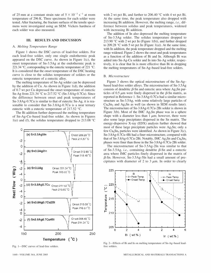
Figure 1 shows the DSC curves of lead-free solders. Foreach lead-free solder, only one single endothermic peakappeared on the DSC curve. As shown in Figure 1(c), theonset temperature of Sn-3.5Ag at the endothermic peak is221.34 °C, corresponding to the eutectic temperature of 221 °C.It is considered that the onset temperature of the DSC heatingcurve is close to the solidus temperature of solders or theeutectic temperature of a eutectic alloy.
The melting temperature of Sn-Ag solder can be depressedby the addition of Cu. As shown in Figure 1(d), the additionof 0.7 wt pct Cu depressed the onset temperature of eutecticSn-Ag from 221.34 °C to 217.52 °C (Sn-3.8Ag-0.7Cu). Sincethe difference between onset and peak temperatures ofSn-3.8Ag-0.7Cu is similar to that of eutectic Sn-Ag, it is rea-sonable to consider that Sn-3.8Ag-0.7Cu is a near ternaryeutectic with a eutectic temperature of 217.52 °C.
The Bi addition further depressed the melting temperatureof Sn-Ag-Cu–based lead-free solder. As shown in Figures1(e) and (f), the solidus temperature dropped to 213.08 °C
with 2 wt pct Bi, and further to 206.40 °C with 4 wt pct Bi.At the same time, the peak temperature also dropped withincreasing Bi addition. However, the melting range, i.e., dif-ference between solidus and peak temperatures, widenedwith increasing Bi addition.
The addition of In also depressed the melting temperatureof Sn-3.5Ag solder. The solidus temperature dropped to213.90 °C with 2 wt pct In (Figure 1(b)), and further droppedto 209.28 °C with 5 wt pct In (Figure 1(a)). At the same time,with In addition, the peak temperature dropped and the meltingrange widened. Figure 2 shows the onset and peak temperaturesas a function of the addition of Bi and In. Although Bi wasadded into Sn-Ag-Cu solder and In into Sn-Ag solder, respec-tively, it is clear that In is more effective than Bi in droppingthe melting temperatures of Sn-Ag–based lead-free solders.
B. Microstructure
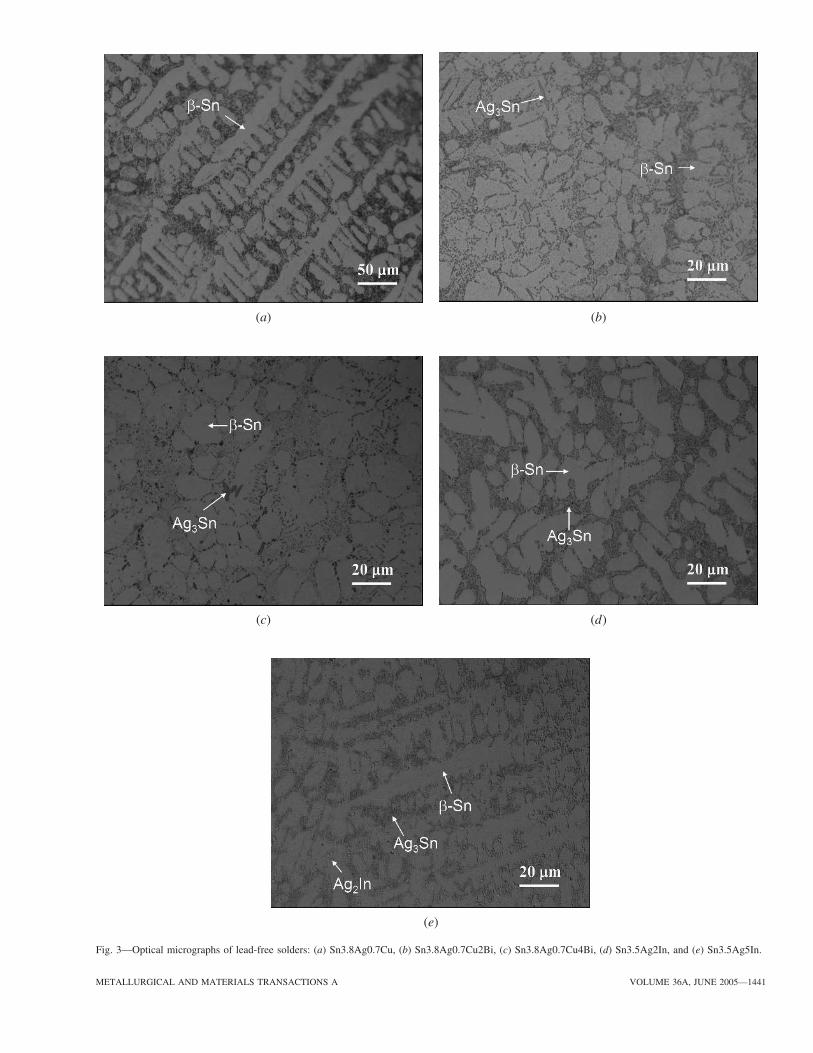
Figure 3 shows the optical microstructure of the Sn-Ag–based lead-free solder alloys. The microstructure of Sn-3.5Agconsists of dendritic �-Sn and eutectic area where Ag3Sn par-ticles of 0.5 �m were finely dispersed in the �-Sn matrix, asreported in Reference 1. Sn-3.8Ag-0.7Cu had a similar micro-structure as Sn-3.5Ag, with some relatively large particles ofCu6Sn5 and Ag3Sn as well (as shown in SEM results later).The microstructure of Sn-3.8Ag-0.7Cu-2Bi solder is shown inFigure 3(b). Most of the IMC Ag3Sn phase was in a sphereshape with a diameter less than 1 �m; however, there werealso some large precipitates dispersed in the Sn matrix. Theenergy-dispersive X-ray (EDX) analysis further showed thatmost of these large precipitate particles were Ag3Sn; only afew Cu6Sn5 particles were identified. As shown in Figure 3(c),Sn-3.8Ag-0.7Cu-4Bi had a finer microstructure, compared withthat of Sn-3.8Ag-0.7Cu-2Bi. Notably, IMC Ag3Sn and Cu6Sn5
phases were finer than those in the Sn-3.8Ag-0.7Cu-2Bi solder.The microstructure of Sn-3.5Ag-2In was similar to that
of Sn-3.5Ag, i.e., containing dendrite �-Sn and a eutecticarea where IMC particles finely dispersed in the matrix of�-Sn. However, Sn-3.5Ag-5In had a small amount of pre-cipitates with diameter of 2 to 3 �m. In order to clearly
Fig. 1—DSC curves of lead-free solders.Fig. 2—Effects of Bi and In on melting temperature of Sn-Ag–based lead-free solders.
METALLURGICAL AND MATERIALS TRANSACTIONS A VOLUME 36A, JUNE 2005—1441
(a) (b)
(c) (d )
(e)
Fig. 3—Optical micrographs of lead-free solders: (a) Sn3.8Ag0.7Cu, (b) Sn3.8Ag0.7Cu2Bi, (c) Sn3.8Ag0.7Cu4Bi, (d) Sn3.5Ag2In, and (e) Sn3.5Ag5In.
1442—VOLUME 36A, JUNE 2005 METALLURGICAL AND MATERIALS TRANSACTIONS A
(b)
(c) (d )
(e)
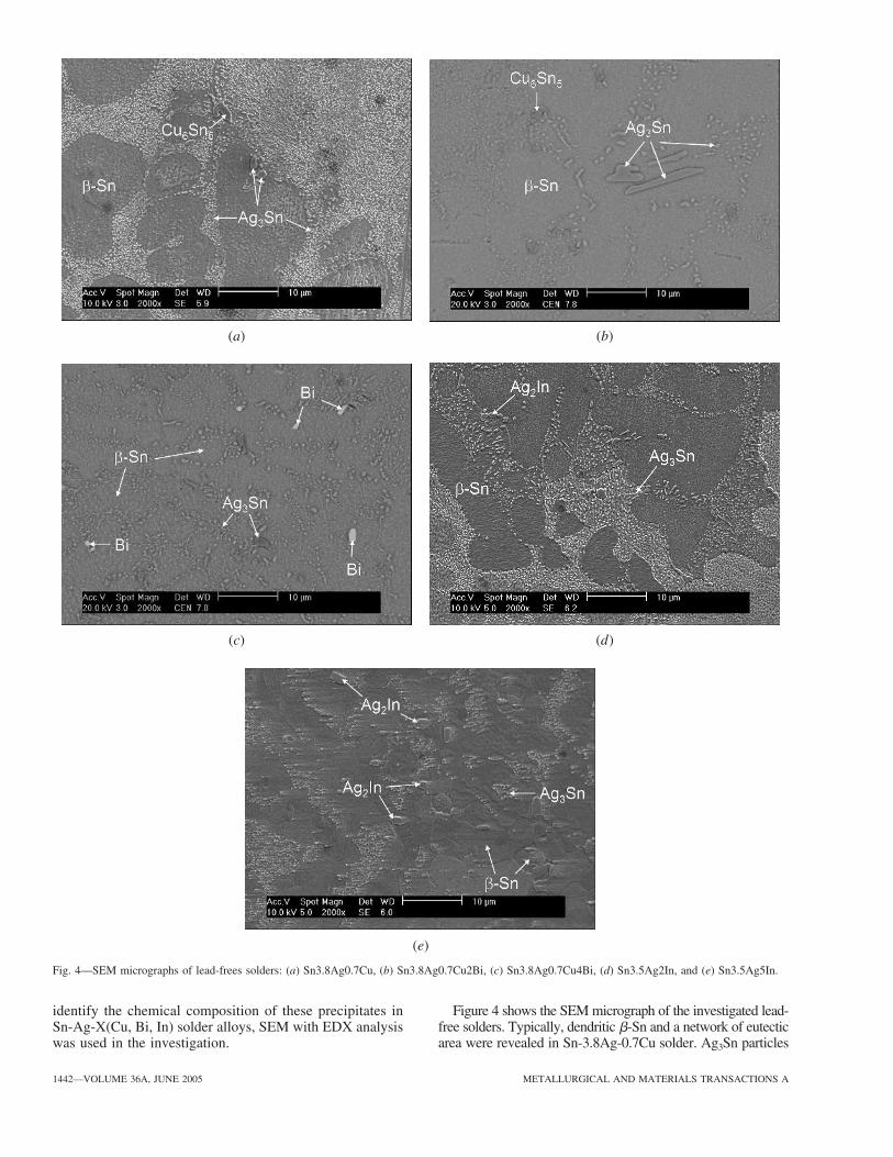
Fig. 4—SEM micrographs of lead-frees solders: (a) Sn3.8Ag0.7Cu, (b) Sn3.8Ag0.7Cu2Bi, (c) Sn3.8Ag0.7Cu4Bi, (d) Sn3.5Ag2In, and (e) Sn3.5Ag5In.
(a)
identify the chemical composition of these precipitates inSn-Ag-X(Cu, Bi, In) solder alloys, SEM with EDX analysiswas used in the investigation.
Figure 4 shows the SEM micrograph of the investigated lead-free solders. Typically, dendritic �-Sn and a network of eutecticarea were revealed in Sn-3.8Ag-0.7Cu solder. Ag3Sn particles
METALLURGICAL AND MATERIALS TRANSACTIONS A VOLUME 36A, JUNE 2005—1443
of 0.5 �m in diameter finely dispersed in the eutectic area.However, some large particles of Cu6Sn5 and Ag3Sn werealso identified (Figure 4(a)). The microstructure of Sn-3.8Ag-0.7Cu solder in the present work is similar to the Sn-3.7Ag-0.9Cu solder joint (cooling rate was 1 to 3 K/s) prepared byAnderson et al.[4,5] The microstructure of Sn-3.8Ag-0.7Cu sol-der in the present work is also similar to the Sn-3.5Ag-0.9Cu/Cusolder joint prepared by reflow soldering rather than the bulkSn-3.5Ag-0.9Cu solder prepared by casting by Allen et al.[12]
Backscattered electron SEM images were used to discernBi distribution in Sn-3.8Ag-0.7Cu-XBi solders. Figures 4(b)and (c) show the backscattered electron SEM images of Sn-3.8Ag-0.7Cu-2Bi and Sn-3.8Ag-0.7Cu-4Bi, respectively. Itis clear that no Bi particle was observed in the Sn-3.8Ag-0.7Cu-2Bi solder, while a very small amount of precipitatedBi particles in Sn-3.8Ag-0.7Cu-4Bi can be observed. It isconcluded that the solid solubility limit of Bi in Sn-matrixat room temperature is about 4 wt pct. If Bi is below 4 wtpct in the solder, Bi will dissolve in Sn matrix. Figure 4(b)shows that there were some Ag3Sn particles (Cu6Sn5 as well)with a relatively large size in the Sn-3.8Ag-0.7Cu-2Bi solder,while smaller precipitates of Ag3Sn and Cu6Sn5 wereobserved in the Sn-3.8Ag-0.7Cu-4Bi solder (Figure 4(c)).The Bi addition obviously suppressed the formation of largeAg3Sn from the Sn-Ag-Cu matrix, which was also observedin References 13 and 14.
Figures 4(d) and (e) show the SEM micrographs of Sn-3.5Ag-2In and Sn-3.5Ag-5In lead-free solders, respectively.The addition of In into Sn-3.5Ag solder resulted in a dif-ference in microstructure; i.e., there were many particles of2 to 3 �m in diameter dispersed in the matrix of Sn-3.5Ag-XIn solder. The EDX analysis showed that these particleswere IMC Ag2In.
C. Tensile Properties
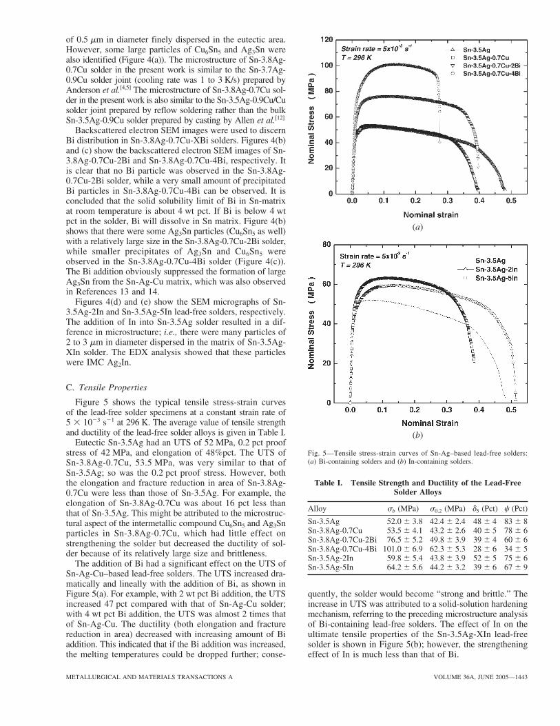
Figure 5 shows the typical tensile stress-strain curvesof the lead-free solder specimens at a constant strain rate of5 � 10�3 s�1 at 296 K. The average value of tensile strengthand ductility of the lead-free solder alloys is given in Table I.
Eutectic Sn-3.5Ag had an UTS of 52 MPa, 0.2 pct proofstress of 42 MPa, and elongation of 48%pct. The UTS ofSn-3.8Ag-0.7Cu, 53.5 MPa, was very similar to that ofSn-3.5Ag; so was the 0.2 pct proof stress. However, boththe elongation and fracture reduction in area of Sn-3.8Ag-0.7Cu were less than those of Sn-3.5Ag. For example, theelongation of Sn-3.8Ag-0.7Cu was about 16 pct less thanthat of Sn-3.5Ag. This might be attributed to the microstruc-tural aspect of the intermetallic compound Cu6Sn5 and Ag3Snparticles in Sn-3.8Ag-0.7Cu, which had little effect onstrengthening the solder but decreased the ductility of sol-der because of its relatively large size and brittleness.
The addition of Bi had a significant effect on the UTS ofSn-Ag-Cu–based lead-free solders. The UTS increased dra-matically and lineally with the addition of Bi, as shown inFigure 5(a). For example, with 2 wt pct Bi addition, the UTSincreased 47 pct compared with that of Sn-Ag-Cu solder;with 4 wt pct Bi addition, the UTS was almost 2 times thatof Sn-Ag-Cu. The ductility (both elongation and fracturereduction in area) decreased with increasing amount of Biaddition. This indicated that if the Bi addition was increased,the melting temperatures could be dropped further; conse-
quently, the solder would become “strong and brittle.” Theincrease in UTS was attributed to a solid-solution hardeningmechanism, referring to the preceding microstructure analysisof Bi-containing lead-free solders. The effect of In on theultimate tensile properties of the Sn-3.5Ag-XIn lead-freesolder is shown in Figure 5(b); however, the strengtheningeffect of In is much less than that of Bi.
(b)
Fig. 5—Tensile stress-strain curves of Sn-Ag–based lead-free solders:(a) Bi-containing solders and (b) In-containing solders.
(a)
Table I. Tensile Strength and Ductility of the Lead-FreeSolder Alloys
Alloy �b (MPa) �0.2 (MPa) �5 (Pct) � (Pct)
Sn-3.5Ag 52.0 � 3.8 42.4 � 2.4 48 � 4 83 � 8Sn-3.8Ag-0.7Cu 53.5 � 4.1 43.2 � 2.6 40 � 5 78 � 6Sn-3.8Ag-0.7Cu-2Bi 76.5 � 5.2 49.8 � 3.9 39 � 4 60 � 6Sn-3.8Ag-0.7Cu-4Bi 101.0 � 6.9 62.3 � 5.3 28 � 6 34 � 5Sn-3.5Ag-2In 59.8 � 5.4 43.8 � 3.9 52 � 5 75 � 6Sn-3.5Ag-5In 64.2 � 5.6 44.2 � 3.2 39 � 6 67 � 9
1444—VOLUME 36A, JUNE 2005 METALLURGICAL AND MATERIALS TRANSACTIONS A
(d )
(e) ( f )
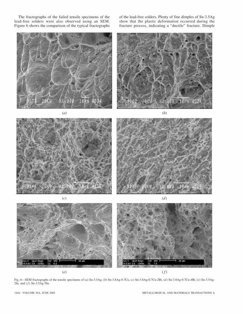
Fig. 6—SEM fractographs of the tensile specimens of (a) Sn-3.5Ag, (b) Sn-3.8Ag-0.7Cu, (c) Sn-3.8Ag-0.7Cu-2Bi, (d ) Sn-3.8Ag-0.7Cu-4Bi, (e) Sn-3.5Ag-2In, and ( f ) Sn-3.5Ag-5In.
(a) (b)
(c)
The fractographs of the failed tensile specimens of thelead-free solders were also observed using an SEM.Figure 6 shows the comparison of the typical fractographs
of the lead-free solders. Plenty of fine dimples of Sn-3.5Agshow that the plastic deformation occurred during thefracture process, indicating a “ductile” fracture. Dimple
METALLURGICAL AND MATERIALS TRANSACTIONS A VOLUME 36A, JUNE 2005—1445
patterns also appeared in the specimens of Sn-3.8Ag-0.7Cuand Sn-3.8Ag-0.7Cu-2Bi; however, the number of dimplesdeceased with increasing alloying additions. In the tensilespecimen of Sn-3.8Ag-0.7Cu-4Bi, no typical dimple wasobserved. Similar results were observed for Sn-3.5Ag-XIn,showing less ductile characteristics occurring during thefracture process with increasing In addition. In general,fractographs showed a ductile feature in Sn-3.5Ag, and thefracture surfaces gradually transferred from ductile to brittlewith increasing additions of Cu, Bi, and In, which was con-sistent with the ductility of the Sn-Ag–based solders in thepreceding tensile tests.
The tensile properties of lead-free solders are not in goodagreement,[15–20] which is attributed to the difference in sam-ple preparation (cooling rate) and test condition (temperature,strain rate, and specimen geometry).
Microstructural variation resulting from different coolingrates is one of the significant factors that influences themechanical properties. The effects of cooling rate onmicrostructure and tensile properties of a Sn-3.5Ag solderwere investigated by Ochoa et al.[15] at a strain rate of 10�3
s�1 in bulk dog-boned specimens. Three cooling rates wereobtained by cooling specimens in the furnace (0.08 K/s), air(0.5 K/s), and water (24 K/s). They found that the UTSseemed unaffected by the cooling rate and yield strengthincreased with increasing cooling rate. The UTSs were about30 MPa in their study, which were lower than that of Sn-3.5Ag in the present work. Sigelko et al.[16] examined Sn-3.5Ag/Cu joints at cooling rates of 2.3 K/s (140 °C/s) and5.5 K/s (330 °C/s). They reported that the dendrite size andorientation did not significantly affect the mechanical prop-erties of the solder joints in the range of cooling rates studied.It is quite possible that the range of cooling rates (2.3 and5.5 K/s) studied by Sigelko et al. was not sufficient to inducea significant change in microstructure and, thus, in mechan-ical properties.
Shohji et al.[17] studied the tensile properties of three Sn-Ag–based lead-free solders in bulk dog-boned specimensprepared under a cooling rate of 10 K/s. The tensile strengthsof the solders increased with decreasing temperatures rangingfrom �40 °C/s to 120 °C/s, and with increasing strain rate.The tensile strength of Sn-3.5Ag at a strain rate of 1.67 �10�3 s�1 at 20 °C was about 40 MPa in their study, whichis slightly lower than that of Sn-3.5Ag in the present work.
Kim et al.[18] carried out a tensile test of a Sn-3Ag-0.5Cusolder at a strain rate of 3.5 � 10�3 s�1 in bulk dog-bonedspecimens prepared under a cooling rate of 8 K/s. The UTSwas 44 MPa and 0.2 pct proof stress was 37 MPa, which areslightly lower than the data of Sn-3.8Ag-0.7Cu obtained inthe present work. This can be explained by less Ag and Cucontents in Sn-3Ag-0.5Cu in their study compared with theSn-3.8Ag-0.7Cu in the present work.
Amagai et al.[19] studied Sn-3.5Ag-0.75Cu solder at threestrain rates (1 to 100 mm/min) in bulk cylindrical specimensprepared by casting into aluminum molds. The tensilestrength, which increased with increasing strain rate, was43 MPa at a strain rate of 3.3 � 10�3 s�1 (10 mm/min). Thetensile data obtained in their study are slightly lower thanthat of the Sn-3.8Ag-0.7Cu in the present work.
Sigelko and Subramanian[20] reported that the UTS of Sn-3.5Ag solder was 55 MPa, which is a little higher than thatof the Sn-3.5Ag solder in the present work.
D. Vickers Hardness
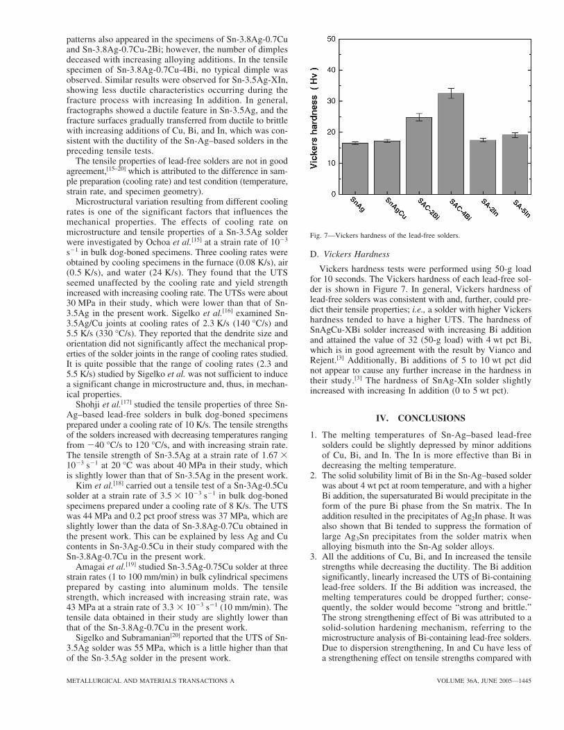
Vickers hardness tests were performed using 50-g loadfor 10 seconds. The Vickers hardness of each lead-free sol-der is shown in Figure 7. In general, Vickers hardness oflead-free solders was consistent with and, further, could pre-dict their tensile properties; i.e., a solder with higher Vickershardness tended to have a higher UTS. The hardness ofSnAgCu-XBi solder increased with increasing Bi additionand attained the value of 32 (50-g load) with 4 wt pct Bi,which is in good agreement with the result by Vianco andRejent.[3] Additionally, Bi additions of 5 to 10 wt pct didnot appear to cause any further increase in the hardness intheir study.[3] The hardness of SnAg-XIn solder slightlyincreased with increasing In addition (0 to 5 wt pct).
IV. CONCLUSIONS
1. The melting temperatures of Sn-Ag–based lead-freesolders could be slightly depressed by minor additionsof Cu, Bi, and In. The In is more effective than Bi indecreasing the melting temperature.
2. The solid solubility limit of Bi in the Sn-Ag–based solderwas about 4 wt pct at room temperature, and with a higherBi addition, the supersaturated Bi would precipitate in theform of the pure Bi phase from the Sn matrix. The Inaddition resulted in the precipitates of Ag2In phase. It wasalso shown that Bi tended to suppress the formation oflarge Ag3Sn precipitates from the solder matrix whenalloying bismuth into the Sn-Ag solder alloys.
3. All the additions of Cu, Bi, and In increased the tensilestrengths while decreasing the ductility. The Bi additionsignificantly, linearly increased the UTS of Bi-containinglead-free solders. If the Bi addition was increased, themelting temperatures could be dropped further; conse-quently, the solder would become “strong and brittle.”The strong strengthening effect of Bi was attributed to asolid-solution hardening mechanism, referring to themicrostructure analysis of Bi-containing lead-free solders.Due to dispersion strengthening, In and Cu have less ofa strengthening effect on tensile strengths compared with
Fig. 7—Vickers hardness of the lead-free solders.
1446—VOLUME 36A, JUNE 2005 METALLURGICAL AND MATERIALS TRANSACTIONS A
that of Bi. In general, fractographs of Sn-3.5Ag-X(Cu,Bi, In) solders gradually transferred from ductile to brittlefeature with increasing third elements.
4. Vickers hardness of lead-free solders was consistent withtheir tensile properties; i.e., a solder with higher Vickershardness tended to have a higher UTS.
ACKNOWLEDGMENTS
One of the authors (MLH) thanks the financial supportfrom the Foundation of Science and Technology (LiaoningProvince, People’s Republic of China), under Grant No.20021067.
REFERENCES1. M.L. Huang, L. Wang, and C.M.L. Wu: J. Mater. Res., 2002, vol. 17,
pp. 2897-03.2. Y. Kariya and M. Otsuka: J. Electron. Mater., 1998, vol. 27, pp. 1129-235.3. P.T. Vianco and J.A. Rejent: J. Electron. Mater., 1999, vol. 28,
pp. 1138-43.4. I.E. Anderson, B.A. Cook, J.L. Harringa, and R.L. Terpstra: JOM,
2002, vol. 6, pp. 26-29.
5. I.E. Anderson, B.A. Cook, J.L. Harringa, and R.L. Terpstra: J. Electron.Mater., 2002, vol. 31, pp. 1166-74.
6. C.M.L. Wu, M.L. Huang, J.K.L. Lai, and Y.C. Chan: J. Electron.Mater., 2000, vol. 29, pp. 1015-20.
7. M.L. Huang, C.M.L. Wu, J.K.L. Lai, and Y.C. Chan: J. Electron.Mater., 2000, vol. 29, pp. 1021-26.
8. M. McCormack and S. Jin: J. Electron. Mater., 1994, vol. 23, pp. 635-40.9. M. McCormack and S. Jin: J. Electron. Mater., 1994, vol. 23, pp. 715-20.
10. D.M. Jacobson and G. Humpston: GEC J. Res., 1995, vol. 12 (2), pp. 112-21.11. M.S. Yeh: Metall. Mater. Trans. A, 2003, vol. 34A, pp. 361-65.12. S.L. Allen, M.R. Notis, R.R. Chromik, and R.P. Vinci: J. Mater. Res.,
2 2004, vol. 19, pp. 1417-24.13. J.W. Jang, D.R. Frear, T.Y. Lee, and K.N. Tu: J. Appl. Phys., 2000,
vol. 88, pp. 6359-63.14. C.M.L. Wu and M.L. Huang: IEEE Trans. Adv. Packaging, 2005,
vol. 28(1), pp. 128-33.15. F. Ochoa, J.J. Williams, and N. Chawla: J. Electron. Mater., 2003,
vol. 32, pp. 1414-20.16. J. Sigelko, S. Choi, K.N. Subramanian, J.P. Lucas, and T.R. Bieler:
J. Electron. Mater., 1999, vol. 28, pp. 1184-88.17. I. Shohji, T. Yoshida, T. Takahashi, and S. Hioki: Mater. Sci. Eng. A,
2004, vol. A366, pp. 50-55.18. K.S. Kim, S.H. Huh, and K. Suganuma: Microelectron. Reliability,
2003, vol. 43, pp. 259-67.19. M. Amagai, M. Watanabe, M. Omiya, K. Kishumoto, and T. Shibuya:
Microelectron. Reliability, 2002, vol. 42, pp. 951-66.20. J. Sigelko and K.N. Subramanian: Adv. Mater. Processes, Mar. 2000,
pp. 47-48.