A Flexible Metamaterial Based Printed Antenna for Wearable ...
Upload
independentCategory
view
2download
0
PHYSICAL REVIEW B 88, 195203 (2013)
Effect of local field enhancement on the nonlinear terahertz responseof a silicon-based metamaterial
Ibraheem Al-Naib,1,* Gargi Sharma,1 Marc M. Dignam,2 Hassan Hafez,1 Akram Ibrahim,1 David G. Cooke,3
Tsuneyuki Ozaki,1 and Roberto Morandotti1,†1INRS-EMT, 1650 Boulevard Lionel-Boulet, Varennes, Quebec J3X 1S2, Canada
2Department of Physics, Engineering Physics and Astronomy, Queen’s University, Kingston, Ontario K7L 3N6, Canada3Department of Physics, McGill University, Montreal, Quebec H3A 2T8, Canada
(Received 9 December 2012; revised manuscript received 15 October 2013; published 13 November 2013)
We demonstrate the strong effect of the local field enhancement on the nonlinear terahertz response of ahybrid photoexcited silicon/double concentric ring metamaterial structure. The ring resonators enhance the localterahertz electric field by more than a factor of ten, pushing the terahertz-semiconductor interaction into thehigh-field regime even for moderate-strength incident terahertz pulses. In this regime, terahertz field-inducedintervalley scattering in the photoexcited silicon substrate dynamically alters the substrate conductivity, whichin turn strongly modifies the pulse transmission. The spatial distribution of the local field enhancement withinthe resonator structure results in a modified bandwidth, amplitude, and central frequency of the transmissionresonance occurring on a subcycle time scale. These results demonstrate an enhancement of the nonlinear terahertzresponse of silicon-based metamaterials that must be accounted for in the design of terahertz nonlinear devices.
DOI: 10.1103/PhysRevB.88.195203 PACS number(s): 41.20.Jb, 46.40.Ff, 78.20.Ci, 78.47.−p
I. INTRODUCTION
Metamaterials are structures engineered to exhibit tailoredelectromagnetic properties such as negative refraction,1,2 sub-diffraction limited imaging,3 and electromagnetic cloaking,4
which are all exciting functionalities that are not available innatural materials. Consequently, they have attracted significantattention over the past decade. The majority of terahertz(THz) metamaterials demonstrated to date5–7 have been fixedstructures whose behavior is dictated by their geometries andthus act as passive devices.8 Controlling THz metamaterialsdynamically is highly desirable, and indeed thermal,9,10
electrical,11,12 and optical13–15 schemes have been proposed toachieve some degree of active control. Photoexcitation of splitring resonators (SRRs) on top of an intrinsic GaAs wafer hasbeen shown to lead to dynamically switched THz radiation.13
The recovery of this switching occurs on a nanosecond timescale, which is the photocarrier lifetime in GaAs. Anotherinteresting approach that has been proposed is to incorporatesemiconducting silicon material in two stripes near the splitgap. When photoexcited, the stripes modify the capacitance ofthe structure and the response can be dynamically tuned.14,15
The characteristic response times of the above-mentioned THzdevices are often slow in relation to the picosecond period ofTHz light. Just as the control of light with light is a majorgoal in contemporary photonics, it would be a significantadvance if one could design THz devices that have a strongnonlinear response to the THz field itself. Such nonlinearmetamaterials offer another degree of freedom in order toachieve dynamically controlled devices.16 Nonlinear behaviorin terahertz metamaterials has been recently demonstrated byemploying vanadium dioxide,17 GaAs,18 and superconductingmetamaterials.19 Clearly, the ability to dynamically control theresponse of such devices in “real time” is highly desirable andexploiting the nonlinear carrier response in silicon using stan-dard semiconductor industry techniques represents a potentialroute to achieve this fundamental goal.
Silicon, the key material in electronics, is an indirect bandgap semiconductor with multiple valleys in the conductionband. When excited with an 800-nm laser pulse, electronsare photoexcited to the X valley of the conduction bandby a phonon-assisted process. The carriers’ energy increaseswhen they interact with intense THz electric fields, and whenthe carriers gain enough kinetic energy to overcome theintervalley difference level (EXL = 0.8 eV), they can scatterto the L valley. Because the higher effective masses in thesatellite valleys decrease the mobility of carriers, the effectiveconductivity of the semiconductor decreases, which resultsin an increase in transmission. A very similar effect has beenstudied and modeled in GaAs in a number of recent papers.20,21
If metamaterials are structured on a silicon substrate, a fieldenhancement that depends on the THz frequency and on thegeometry of the structure will take place inside silicon. Thisin turn will increase THz induced intervalley scattering insidethe sample. Hence we expect that, whenever the metamaterialstructure on the silicon substrate is photoinjected with carriers,the THz transmission will be strongly affected by the intenseTHz electric field itself, especially at the resonance frequency.
In this work, which follows our initial experimentalresults,22 we present a thorough investigation of silicon-basedultrafast nonlinear terahertz metamaterials. The structure weexamine here consists of an array of gold concentric ringresonators deposited on an optically pumped high-resistivitysilicon wafer. We show experimentally that the transmissionof a short-pulse THz field through the structure stronglydepends on the intensity of the THz field. This demonstratesnot only that the structure has a strong nonlinear responseat THz frequencies but also that the response occurs on asubcycle time scale. By comparing the experimental resultswith simulations, we show that the nonlinearity dependscritically on the THz-induced reduction of the conductivityof the photoexcited silicon due to the strong enhancement ofthe THz field near the resonators. Using this effect, one could
195203-11098-0121/2013/88(19)/195203(8) ©2013 American Physical Society
IBRAHEEM AL-NAIB et al. PHYSICAL REVIEW B 88, 195203 (2013)
in principle use a relatively weak THz field to modulate thesystem response on a subcycle time scale.
II. LINEAR THz RESPONSE OF BARE SILICONAND THE METAMATERIAL SYSTEM
The unit cell of our metamaterial resonator array consistsof two concentric gold ring resonators (CRRs). This CRRstructure has been chosen because it exhibits an angle- andpolarization-independent response that is very desirable for awide range of applications,6,7 unlike typical SRR-based de-signs, which show a strong angular dependence.23 Moreover,the horizontal and vertical polarization responses of SRRs arequite different due to their spatial asymmetry. Furthermore,the CRR configuration exhibits an electromagnetic inducedtransparency (EIT)-like response that makes it an intriguingcandidate to be used in “slow light” applications.6 For ourpurpose, its strong spatial field localization can potentiallyenhance the optical nonlinearities. The unit cell of the CRRtogether with its relevant dimensions is illustrated in Fig. 1(a).When the silicon substrate is not optically pumped, thestructure resonates at 0.7 THz. The resonators are patternedon a 200-nm layer of gold deposited on a high-resistivity(8400 � · cm) silicon substrate with a thickness of 3 mm.The electric field at the resonance frequency (calculated usingthe frequency domain solver in CST Microwave Studio) isdepicted in Fig. 1(b). The resonant mode takes the shape of anelliptical eye with a linearly polarized excitation field orientedhorizontally along the major axis—as shown in the inset of
FIG. 1. (Color online) (a) A photograph of the unit cell of the CRRwith the relevant dimensions: a lattice constant of p = 125 μm, anouter resonator radius of r = 30 μm, a resonator width of w = 5 μm,and a gap of g = 10 μm. The axes on the figure indicate the orientationof the exciting THz field. (b) Simulated spatial electric field at theresonance. (c) The measured transmission of photoexcited siliconwith the Drude fit. (d) The measured and simulated transmissionresponse for the unpumped metamaterial sample as well as for thepumped sample. As the pump fluence is increased, the resonancefrequency is blue-shifted and the transmission at resonance is reduceddue to the change in the imaginary and real parts of the conductivityof the silicon, respectively.
Fig. 1(a), with a high-field confinement around the right andleft parts of the outer ring. On resonance, the field is enhancedby approximately a factor of ten near the outer concentric circleof the resonator.
As a benchmark, we first measured the THz transmissionthrough photoexcited bare silicon. These measurements weretaken using the same setup that will be described later on butwith a very weak THz pulse, which results in an essentiallylinear THz response. All measurements were performed ina dry N2 purged environment in order to prevent absorptionby atmospheric humidity. In all that follows, the transmissionspectra are determined as the ratio of the Fourier spectra ofthe transmitted THz field to the incident one. Fig. 1(c) (dashedcurve) shows the measured transmission for an optical pumpat a wavelength of 800 nm and a fluence of 14.6 μJ/cm2,which corresponds to a carrier density of 3.4 × 1016 cm−3.The probing THz field here is weak (∼0.4 kV/cm) so as toavoid any nonlinearity in the response of the carriers. Theconductivity of the pumped silicon layer is modeled usingthe Drude model with a carrier density of 3.6 × 1016 cm−3
and a scattering time of 200 fs. As can be seen from thesolid line in Fig. 1(c), this model accurately reproduces theexperimental transmission, which demonstrates that we arein the linear THz regime, where a simple Drude model isapplicable.
We now turn to the low-field linear response of themetamaterial system. Figure 1(d) shows the measured low-field (∼0.4 kV/cm) transmission of the metamaterial samplewhen there is no optical pumping (dotted), for an 800 nmoptical pump (40-fs pulse duration) fluence of 5.3 μJ/cm2
(dash-dot) and for an optical pump fluence of 14.6 μJ/cm2
(dashed). Also shown is a simulation (solid) of the unpumpedsample. As can be seen, the agreement between experimentand simulation is very good. When the sample is opticallypumped at the lower fluence (5.3 μJ/cm2), we clearly seetwo effects. First, there is a strong blue shift of 69 GHz inthe resonance frequency that is in agreement with previousworks.13,24 This is due to the pump-induced change in theimaginary part of the conductivity of the silicon, which inturn modifies the capacitance of the resonator. Second, thequality (Q) factor of the resonance is greatly reduced. Thisis due to an increase in the real part of the conductivity,which increases the losses in the system. These two effectsdemonstrate that the THz transmission is strongly dependenton the effective conductivity of the silicon. When we move tothe higher pump fluence (14.6 μJ/cm2), the decrease in the Q
factor is so large that the position of the resonance is difficult todiscern. It should be blue shifted even more, yet the resonanceat 0.7 THz is now clearly suppressed. This shows that if onecould modulate the effective conductivity using the THz fielditself, the nonlinear response at the resonant frequency couldbe very large; this is indeed the desirable effect that we shallnow examine in our high-field THz experiments in bare siliconand for the metamaterial structure.
III. NONLINEAR THz RESPONSE OF BARE SILICON
We now turn to the high-field THz measurements that werecarried out using an optical-pump terahertz-probe (OPTP)setup coupled to the intense THz source,25 available at
195203-2

EFFECT OF LOCAL FIELD ENHANCEMENT ON THE NONLINEAR . . . PHYSICAL REVIEW B 88, 195203 (2013)
FIG. 2. (Color online) Schematic of the optical-pump terahertz-probe realized with a LiNbO3 high-power THz source based on thetilted-pulse-front technique.
the Advanced Laser Light Source (ALLS) facility recentlyestablished at INRS-EMT. The source generates intense THzpulses using a tilted-pulse-front technique by employing aLiNbO3 crystal.26 The experimental setup is depicted in Fig. 2.An 800 nm laser beam with energy of 1.55 mJ, 40-fs pulseduration and repetition rate of 2.5 kHz is used. The first beamsplitter (BS1) divides the laser beam into a generation beamand a probe beam. The generation beam is used to induce theTHz signal from the LiNbO3 crystal. The diffracted beam fromthe grating is imaged onto the crystal with a demagnificationfactor of 1.7, using an achromatic lens with a focal length of150 mm. The second beam splitter (BS2) further divides theprobe beam into two equal parts. The reflected part of the beamis sent to the first delay stage, which is then used to forwardthe beam to optically pump the sample. The transmitted partof the probe beam is sent to a second delay stage, whichis then used as an optical probe beam to detect the THzpulse. Two wire-grid polarizers are used to change the THzelectric field. The transmitted signal is detected using freespace electro-optic sampling and a 3-mm-thick ZnTe crystal.The thick ZnTe crystal is used to achieve a high spectralresolution by taking long scans across a temporal windowof 65 ps, in order to resolve any modification in the spectral
response. To avoid over-rotation in the electro-optic detectionat high THz field strengths, two high resistivity silicon wafersare placed before the detection ZnTe crystal to reduce theTHz electric field by as much as 49%. The maximum THzfield is estimated using Eq. (1) in Ref. 21. The THz spot sizemeasured using a pyroelectric camera (ElectroPhysics, modelPV320) is found to be 1.2 mm at FWHM, while the THz energyhas been found to be 0.145 μJ, measured using a MicrotechInstrument pyroelectric detector. The electric field is evaluatedto be 90 kV/cm at the sample position.
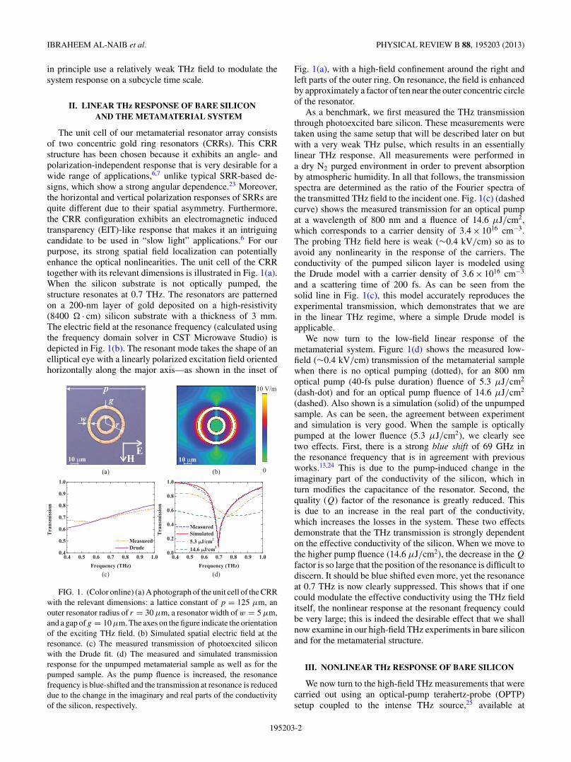
Next, we present the bare silicon transmission resultsand show that the effect of the THz field is to reducethe conductivity and to produce a clearly non-Drude-likeconductivity in the pumped silicon layer at the surface. Thephotoexcited bulk silicon wafer is schematically depicted inFig. 3(a), indicating the exponential decay of the density ofphotogenerated carriers as we move away from the surface.To ensure that a steady state carrier density has been formed,the pump pulse is timed to arrive 10 ps before the peak ofthe THz waveform. Measurements of this photoexcited baresilicon were performed at the following four different THzlevels: 11, 41, 70, and 90 kV/cm. The resulting transmissionspectra are shown in Fig. 3(b). As can be seen, the transmissionat 0.7 THz becomes ∼13% higher when the THz electric fieldis increased. This increase is attributed to the bleaching ofthe THz absorption due to intervalley scattering of electronsin the conduction band similar to earlier observation inGaAs.21 Note that the photoinjected carrier density decaysoff exponentially over a distance given by the optical skindepth of d = 10 microns at a pump wavelength of 800 nm.Because this depth is an appreciable fraction of the wavelengthof the THz field in the silicon, the commonly used thin-film approximation (where the propagation phase change isneglected) cannot be employed to calculate the transmissionthrough the sample. Instead, we modeled the photoexcitedlayer as a multilayer where the phase is included in order tocalculate the transmission and thereby extract the complexconductivity. This procedure is used to determine the realand imaginary parts of conductivity as presented in Figs. 3(c)and 3(d), respectively. What can be seen from this figure isthat the conductivity decreases with increasing THz field. Asdiscussed above, this can be interpreted as arising from theintervalley scattering of carriers.
We note that although the usual thin film model cannotbe used to extract the conductivity, we find that a generallyacceptable approximation is to employ a modified thin filmmodel that includes the propagation phase in the photoexcitedsilicon. Using this model, the ratio of the pumped (τ ) tounpumped (τnp) transmission is given by
τ
τnp= 2(1 + nsi)e−ikonsid
[(1 + nc + nsi + nsi/nc)e−ikoncd + (1 − nc + nsi − nsi/nc)e+ikoncd ], (1)
nc =√
n2si + i
σ (z = 0,ω)
ωεo
, (2)
195203-3
IBRAHEEM AL-NAIB et al. PHYSICAL REVIEW B 88, 195203 (2013)
FIG. 3. (Color online) (a) Schematic diagram showing the photoexcited layer on the silicon wafer and the penetration depth of d = 10microns at 800-nm wavelength, (b) transmission amplitude for the photoexcited bare silicon wafer at different THz levels, (c) real and(d) imaginary parts of the extracted conductivity for the pumped bare silicon wafer at different THz levels. High electric field enablesintervalley scattering in the conduction band and leads to increase in transmission due to the reduction in conductivity.
where nc and nsi are the refractive indices of the photocon-ductive layer and bulk silicon, respectively, k0 is the wavevector, d is the optical skin depth of the silicon, ω is the radianfrequency, ε0 is the permittivity in free space, and σ is thecomplex conductivity. We use this one-layer model later inour simulations of the silicon conductivity in the metamaterialsystem.
IV. NONLINEAR THz RESPONSE OFTHE METAMATERIAL SYSTEM
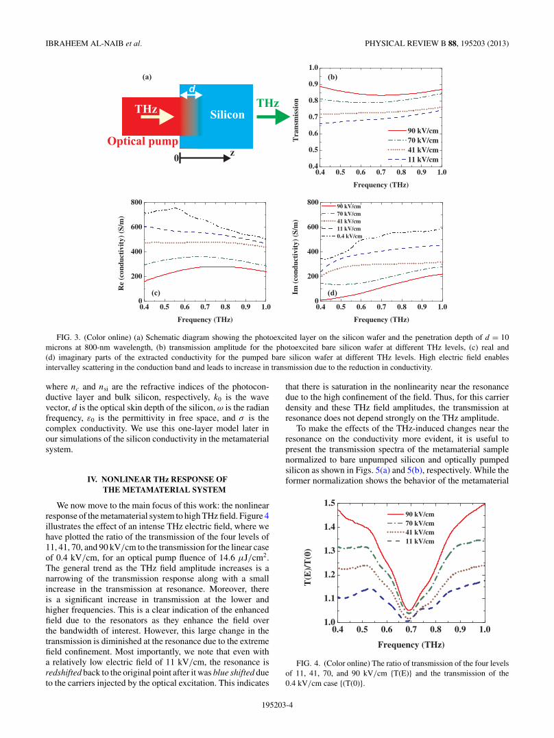
We now move to the main focus of this work: the nonlinearresponse of the metamaterial system to high THz field. Figure 4illustrates the effect of an intense THz electric field, where wehave plotted the ratio of the transmission of the four levels of11, 41, 70, and 90 kV/cm to the transmission for the linear caseof 0.4 kV/cm, for an optical pump fluence of 14.6 μJ/cm2.The general trend as the THz field amplitude increases is anarrowing of the transmission response along with a smallincrease in the transmission at resonance. Moreover, thereis a significant increase in transmission at the lower andhigher frequencies. This is a clear indication of the enhancedfield due to the resonators as they enhance the field overthe bandwidth of interest. However, this large change in thetransmission is diminished at the resonance due to the extremefield confinement. Most importantly, we note that even witha relatively low electric field of 11 kV/cm, the resonance isredshifted back to the original point after it was blue shifted dueto the carriers injected by the optical excitation. This indicates
that there is saturation in the nonlinearity near the resonancedue to the high confinement of the field. Thus, for this carrierdensity and these THz field amplitudes, the transmission atresonance does not depend strongly on the THz amplitude.
To make the effects of the THz-induced changes near theresonance on the conductivity more evident, it is useful topresent the transmission spectra of the metamaterial samplenormalized to bare unpumped silicon and optically pumpedsilicon as shown in Figs. 5(a) and 5(b), respectively. While theformer normalization shows the behavior of the metamaterial
FIG. 4. (Color online) The ratio of transmission of the four levelsof 11, 41, 70, and 90 kV/cm {T(E)} and the transmission of the0.4 kV/cm case {(T(0)}.
195203-4
EFFECT OF LOCAL FIELD ENHANCEMENT ON THE NONLINEAR . . . PHYSICAL REVIEW B 88, 195203 (2013)
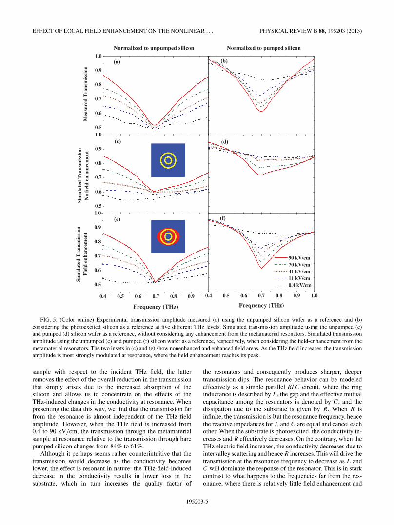
FIG. 5. (Color online) Experimental transmission amplitude measured (a) using the unpumped silicon wafer as a reference and (b)considering the photoexcited silicon as a reference at five different THz levels. Simulated transmission amplitude using the unpumped (c)and pumped (d) silicon wafer as a reference, without considering any enhancement from the metamaterial resonators. Simulated transmissionamplitude using the unpumped (e) and pumped (f) silicon wafer as a reference, respectively, when considering the field-enhancement from themetamaterial resonators. The two insets in (c) and (e) show nonenhanced and enhanced field areas. As the THz field increases, the transmissionamplitude is most strongly modulated at resonance, where the field enhancement reaches its peak.
sample with respect to the incident THz field, the latterremoves the effect of the overall reduction in the transmissionthat simply arises due to the increased absorption of thesilicon and allows us to concentrate on the effects of theTHz-induced changes in the conductivity at resonance. Whenpresenting the data this way, we find that the transmission farfrom the resonance is almost independent of the THz fieldamplitude. However, when the THz field is increased from0.4 to 90 kV/cm, the transmission through the metamaterialsample at resonance relative to the transmission through barepumped silicon changes from 84% to 61%.
Although it perhaps seems rather counterintuitive that thetransmission would decrease as the conductivity becomeslower, the effect is resonant in nature: the THz-field-induceddecrease in the conductivity results in lower loss in thesubstrate, which in turn increases the quality factor of
the resonators and consequently produces sharper, deepertransmission dips. The resonance behavior can be modeledeffectively as a simple parallel RLC circuit, where the ringinductance is described by L, the gap and the effective mutualcapacitance among the resonators is denoted by C, and thedissipation due to the substrate is given by R. When R isinfinite, the transmission is 0 at the resonance frequency, hencethe reactive impedances for L and C are equal and cancel eachother. When the substrate is photoexcited, the conductivity in-creases and R effectively decreases. On the contrary, when theTHz electric field increases, the conductivity decreases due tointervalley scattering and hence R increases. This will drive thetransmission at the resonance frequency to decrease as L andC will dominate the response of the resonator. This is in starkcontrast to what happens to the frequencies far from the res-onance, where there is relatively little field enhancement and
195203-5
IBRAHEEM AL-NAIB et al. PHYSICAL REVIEW B 88, 195203 (2013)
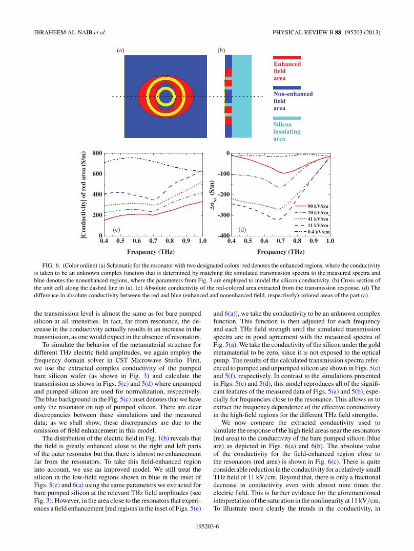
FIG. 6. (Color online) (a) Schematic for the resonator with two designated colors: red denotes the enhanced regions, where the conductivityis taken to be an unknown complex function that is determined by matching the simulated transmission spectra to the measured spectra andblue denotes the nonenhanced regions, where the parameters from Fig. 3 are employed to model the silicon conductivity. (b) Cross section ofthe unit cell along the dashed line in (a). (c) Absolute conductivity of the red-colored area extracted from the transmission response. (d) Thedifference in absolute conductivity between the red and blue (enhanced and nonenhanced field, respectively) colored areas of the part (a).
the transmission level is almost the same as for bare pumpedsilicon at all intensities. In fact, far from resonance, the de-crease in the conductivity actually results in an increase in thetransmission, as one would expect in the absence of resonators.
To simulate the behavior of the metamaterial structure fordifferent THz electric field amplitudes, we again employ thefrequency domain solver in CST Microwave Studio. First,we use the extracted complex conductivity of the pumpedbare silicon wafer (as shown in Fig. 3) and calculate thetransmission as shown in Figs. 5(c) and 5(d) where unpumpedand pumped silicon are used for normalization, respectively.The blue background in the Fig. 5(c) inset denotes that we haveonly the resonator on top of pumped silicon. There are cleardiscrepancies between these simulations and the measureddata; as we shall show, these discrepancies are due to theomission of field enhancement in this model.
The distribution of the electric field in Fig. 1(b) reveals thatthe field is greatly enhanced close to the right and left partsof the outer resonator but that there is almost no enhancementfar from the resonators. To take this field-enhanced regioninto account, we use an improved model. We still treat thesilicon in the low-field regions shown in blue in the inset ofFigs. 5(e) and 6(a) using the same parameters we extracted forbare pumped silicon at the relevant THz field amplitudes (seeFig. 3). However, in the area close to the resonators that experi-ences a field enhancement [red regions in the inset of Figs. 5(e)
and 6(a)], we take the conductivity to be an unknown complexfunction. This function is then adjusted for each frequencyand each THz field strength until the simulated transmissionspectra are in good agreement with the measured spectra ofFig. 5(a). We take the conductivity of the silicon under the goldmetamaterial to be zero, since it is not exposed to the opticalpump. The results of the calculated transmission spectra refer-enced to pumped and unpumped silicon are shown in Figs. 5(e)and 5(f), respectively. In contrast to the simulations presentedin Figs. 5(c) and 5(d), this model reproduces all of the signifi-cant features of the measured data of Figs. 5(a) and 5(b), espe-cially for frequencies close to the resonance. This allows us toextract the frequency dependence of the effective conductivityin the high-field regions for the different THz field strengths.
We now compare the extracted conductivity used tosimulate the response of the high field areas near the resonators(red area) to the conductivity of the bare pumped silicon (blueare) as depicted in Figs. 6(a) and 6(b). The absolute valueof the conductivity for the field-enhanced region close tothe resonators (red area) is shown in Fig. 6(c). There is quiteconsiderable reduction in the conductivity for a relatively smallTHz field of 11 kV/cm. Beyond that, there is only a fractionaldecrease in conductivity even with almost nine times theelectric field. This is further evidence for the aforementionedinterpretation of the saturation in the nonlinearity at 11 kV/cm.To illustrate more clearly the trends in the conductivity, in
195203-6
EFFECT OF LOCAL FIELD ENHANCEMENT ON THE NONLINEAR . . . PHYSICAL REVIEW B 88, 195203 (2013)
Fig. 6(d), we plot the difference (�σ NL) between the extractedconductivity (enhanced field red area) and the conductivityfor bare pumped silicon (nonenhanced field blue area) for thesame THz field strength. As can be seen, the conductivity isreduced for all THz field strengths, with the reduction beingstrongest near the resonance where the field enhancement isthe largest. The reduction in the conductivity becomes largeras the THz field strength is decreased from 90 to 11 kV/cm.This is because �σ NL is almost saturated even in bare siliconfor the maximum field of 90 kV/cm and so the enhancement ofthe field due to the resonator has a relatively small effect. Forintermediate field strengths, the change in the conductivityis the strongest possible, while for the smallest field of0.4 kV/cm, there is very little decrease in the conductivity dueto the fact that in spite of the enhancement near the resonators,the THz field is still too weak to affect the conductivity. Wenote that although the precise values that we obtain for theeffective conductivities near the resonance will depend onthe precise choice of the enhancement region, the trends arerobust.
V. CONCLUSION
In conclusion, we have demonstrated an ultrafast nonlinearchange in the transmission response of a THz metamaterial byemploying intense THz fields. Numerical simulations based ona finite integration technique and a multilayer model along withfar field OPTP measurements verify that this novel ultrafastnonlinear switching can be attributed to the change in the
conductivity of the optically pumped silicon due to THz field-induced intervalley transfer. Due to the large enhancement ofthe THz field near the resonators when we are close to theresonance frequency, we found that for the carrier densitiesand THz field amplitudes employed, there is relatively littlechange in the transmission near the resonant frequency of theresonators. From our results, it is clear that if one wishes tochange the THz field amplitudes at which the conductivitynear the resonance is saturated, one can choose resonatorswith smaller Q factors. This is an important consideration indesigning such structures for nonlinear applications.
Finally, we expect that if a lower level of optical pumpingis used, one would see a strong shift in the transmission dipin addition to an increase in its depth [see Fig. 1(d)]. Thismechanism could be the basis for ultrafast all-THz switching,for example, in future THz based telecom systems, where theswitching pulse is resonant and the signal pulse is nonreso-nant. Due to the confinement-enhanced nonlinearity and therelatively large volume of the resonant mode, the nonlinearresponse at the signal frequency will be much greater than inbare pumped silicon, yielding better switching characteristics.This is clearly an avenue for future investigation.
ACKNOWLEDGMENT
The authors would like to thank the Natural Sciencesand Engineering Research Council of Canada (NSERC) forfinancial support.
*To whom all correspondence should be addressed: [email protected]
†[email protected]. R. Smith, J. B. Pendry, and M. C. K. Wiltshire, Science 305, 788(2004).
2R. A. Shelby, D. R. Smith, and S. Schultz, Science 292, 77 (2001).3N. Fang, H. Lee, C. Sun, and X. Zhang, Science 308, 534 (2005).4D. Schurig, J. J. Mock, B. J. Justice, S. A. Cummer, J. B. Pendry,A. F. Starr, and D. R. Smith, Science 314, 977 (2006).
5V. A. Fedotov, M. Rose, S. L. Prosvirnin, N. Papasimakis, andN. I. Zheludev, Phys. Rev. Lett. 99, 147401 (2007).
6N. Papasimakis, Y. H. Fu, V. A. Fedotov, S. L. Prosvirnin, D. P.Tsai, and N. I. Zheludev, Appl. Phys. Lett. 94, 211902 (2009).
7I. A. I. Al-Naib, C. Jansen, N. Born, and M. Koch, Appl. Phys. Lett.98, 091107 (2011).
8H.-T. Chen, J. F. O’Hara, A. K. Azad, and A. J. Taylor,Laser Photon. Rev. 5, 513 (2011).
9T. Driscoll, S. Palit, M. M. Qazilbash, M. Brehm, F. Keilmann,B.-G. Chae, S.-J. Yun, H.-T. Kim, S. Y. Cho, N. M. Jokerst, D. R.Smith, and D. N. Basov, Appl. Phys. Lett. 93, 024101 (2008).
10R. Singh, A. K. Azad, Q. X. Jia, A. J. Taylor, and H.-T. Chen,Opt. Lett. 36, 1230 (2011).
11H.-T. Chen, W. J. Padilla, J. M. O. Zide, A. C. Gossard, A. J. Taylor,and R. D. Averitt, Nature (London) 444, 597 (2006).
12O. Paul, C. Imhof, B. Lagel, S. Wolff, S. Hofling, A. Forchel,R. Zengerle, and M. Rahm, Opt. Express 17, 819 (2009).
13W. J. Padilla, A. J. Taylor, C. Highstrete, M. Lee, and R. D. Averitt,Phys. Rev. Lett. 96, 107401 (2006).
14H.-T. Chen, J. F. O’Hara, A. K. Azad, A. J. Taylor, R. D. Averitt,D. B. Shrekenhamer, and W. J. Padilla, Nat. Photon. 2, 295(2008).
15N.-H. Shen, M. Massaouti, M. Gokkavas, J.-M. Manceau, E. Ozbay,M. Kafesaki, T. Koschny, S. Tzortzakis, and C. M. Soukoulis,Phys. Rev. Lett. 106, 037403 (2011).
16M. Rahm, J.-S. Li, and W. J. Padilla, J. Infrared, Millimeter,Terahertz Waves 34, 1 (2013).
17M. Liu, H. Y. Hwang, H. Tao, A. C. Strikwerda, K. Fan, G. R.Keiser, A. J. Sternbach, K. G. West, S. Kittiwatanakul, J. Lu, S. A.Wolf, F. G. Omenetto, X. Zhang, K. A. Nelson, and R. D. Averitt,Nature (London) 487, 345 (2012).
18K. Fan, H. Y. Hwang, M. Liu, A. C. Strikwerda, A. Sternbach,J. Zhang, X. Zhao, X. Zhang, K. A. Nelson, and R. D. Averitt,Phys. Rev. Lett. 110, 217404 (2013).
19C. Zhang, B. Jin, J. Han, I. Kawayama, H. Murakami, J. Wu,L. Kang, J. Chen, P. Wu, and M. Tonouchi, Appl. Phys. Lett. 102,081121 (2013).
20F. H. Su, F. Blanchard, G. Sharma, L. Razzari, A. Ayesheshim,T. L. Cocker, L. V. Titova, T. Ozaki, J.-C. Kieffer, R. Morandotti,M. Reid, and F. A. Hegmann, Opt. Express 17, 9620 (2009);L. Razzari, F. H. Su, G. Sharma, F. Blanchard, A. Ayesheshim,H. C. Bandulet, R. Morandotti, J. C. Kieffer, T. Ozaki, M. Reid, andF. A. Hegmann, Phys. Rev. B 79, 193204 (2009).
21G. Sharma, I. Al-Naib, H. Hafez, R. Morandotti, D. G. Cooke, andT. Ozaki, Opt. Express 20, 18016 (2012).
22I. Al-Naib, G. Sharma, M. M. Dignam, D. G. Cooke,T. Ozaki, and R. Morandotti, in IEEE Photonics Conference
195203-7

IBRAHEEM AL-NAIB et al. PHYSICAL REVIEW B 88, 195203 (2013)
(IEEE Photonics Society, IEEE Xplore, Burlingame, CA, USA,2012), p. 554.
23X.-L. Xu, B.-G. Quan, C.-Z. Gu, and L. Wang, J. Opt. Soc. Am. B23, 1174 (2006).
24J.-M. Manceau, N.-H. Shen, M. Kafesaki, C. M. Soukoulis, andT. S. Appl. Phys. Lett. 96, 021111 (2010).
25F. Blanchard, G. Sharma, L. Razzari, X. Ropagnol, H.-C. Bandulet,F. Vidal, R. Morandotti, J.-C. Kieffer, T. Ozaki, H. Tiedje,H. Haugen, M. Reid, and F. A. Hegmann, IEEE J. Sel. Top. QuantumElectron. 17, 5 (2011).
26J. Hebling, G. Almasi, and I. Z. Kozma, Opt. Express 10, 1161(2002).
195203-8
Copyright © 2022 FDOKUMEN