
Dynamically Reconfigurable NoC with Bus Based Interface for Ease of Integration and Reduced Design...
6
Dynamically Reconfigurable NoC with Bus Based Interface for Ease of Integration and Reduced Design Time. Abstract This paper demonstrates our implementation of a dynamically reconfigurable network on chip router with bus based interface. Our work targets heterogeneous integration of components in NoC architecture and includes modeling of reconfigurable components, processor cores and fixed IPs. The novelty of the proposed NoC lies in its ability to integrate standard non-packet based components thus reducing design time and ease of integration. A system consisting of an ARM processor, reconfigurable FFT, reconfigurable Viterbi decoder, memory controller and peripherals is considered with the option of system scalability for future upgrades. A framework for system level modeling of reconfigurable NoC with reconfigurable components is also proposed and demonstrated in systemC. Results are compared with implementation of the same system with conventional NoC to demonstrate advantages of the proposed NoC architecture. I. Introduction Following the prediction of Moore’s law, present day multi-core architectures can accommodate multiple heterogeneous components including reconfigurable, traditional hard coded components and software based running on micro-processors. Network on Chip (NoC) is considered to be a solution to the communication demands imposed by such architecture. NoC is been the subject of research for the last few years however, the pressure of design time, ease of integration, effective resource utilization and misunderstood concepts of NoC makes the system designers reluctant to use NoC as the proffered communication medium. NoC is generated by choosing a network topology, one of the routing and switching schemes and fixing a packet size [1][2][3]. However, along with the advantages of any communication parameter follows its disadvantages and a compromise has to be reached when choosing these network parameters for NOC. A dynamically reconfigurable NoC was proposed [4][5] that eliminates this compromised choice of network parameters and dynamically chooses the best parameter in terms of routing, switching and packet size for the optimized network performance. Keeping in view the problem faced by system integrators when dealing with NoC for communication, the work presented in this paper describes the improvement in the previously proposed NoC architecture for the ease of integration and reduced design time. By giving NoC a bus like interface, use of wrapper is eliminated and any component designed to be integrated to a bus based platform can be integrated in the proposed NoC in plug and play fashion. To demonstrate our approach, a WiMAX system, previously designed with a bus based and cross bar based communication media is implemented with the proposed NoC. Results of the implementation are compared with different communication architectures and a standard NoC with wrappers for integration purposes. A novel systemC modeling framework is also proposed for dynamically reconfigurable NoC and reconfigurable cores integrated in the system. This is useful for quick system verification and simulation. 2. Related Work Many different NoC architectures have been proposed in the last few years, For example, Ethereal[6] SoCIN[7], NOSTRUM[8] and HERMES[9] based on synchronous communication between nodes, other NoC types such as CHAIN[10], NEXUS[11] and ANoC[12] have been proposed based on the Globally Asynchronous Locally Synchronous (GALS) communication. Being a packet based communication media, when integrating the available off the shelf components in the above mentioned NoCs, a wrapper has to be employed as most of the commercial based Balal Ahmad, Ali Ahmadinia, Tughrul Arslan School of Electronics & Engineering University of Edinburgh, King’s Buildings, Mayfield Rd, Edinburgh, EH9 3JL, UK {b.ahmad,a.ahmadinia,t.arslan}@ed.ac.uk NASA/ESA Conference on Adaptive Hardware and Systems 978-0-7695-3166-3/08 $25.00 © 2008 IEEE DOI 10.1109/AHS.2008.38 303 NASA/ESA Conference on Adaptive Hardware and Systems 978-0-7695-3166-3/08 $25.00 © 2008 IEEE DOI 10.1109/AHS.2008.38 309 NASA/ESA Conference on Adaptive Hardware and Systems 978-0-7695-3166-3/08 $25.00 © 2008 IEEE DOI 10.1109/AHS.2008.38 309
-
Upload
independent -
Category
Documents
-
view
1 -
download
0
Transcript of Dynamically Reconfigurable NoC with Bus Based Interface for Ease of Integration and Reduced Design...

Dynamically Reconfigurable NoC with Bus Based Interface for Ease of Integration and Reduced Design Time.
Abstract This paper demonstrates our implementation of a dynamically reconfigurable network on chip router with bus based interface. Our work targets heterogeneous integration of components in NoC architecture and includes modeling of reconfigurable components, processor cores and fixed IPs. The novelty of the proposed NoC lies in its ability to integrate standard non-packet based components thus reducing design time and ease of integration. A system consisting of an ARM processor, reconfigurable FFT, reconfigurable Viterbi decoder, memory controller and peripherals is considered with the option of system scalability for future upgrades. A framework for system level modeling of reconfigurable NoC with reconfigurable components is also proposed and demonstrated in systemC. Results are compared with implementation of the same system with conventional NoC to demonstrate advantages of the proposed NoC architecture. I. Introduction
Following the prediction of Moore’s law, present day multi-core architectures can accommodate multiple heterogeneous components including reconfigurable, traditional hard coded components and software based running on micro-processors. Network on Chip (NoC) is considered to be a solution to the communication demands imposed by such architecture. NoC is been the subject of research for the last few years however, the pressure of design time, ease of integration, effective resource utilization and misunderstood concepts of NoC makes the system designers reluctant to use NoC as the proffered communication medium.
NoC is generated by choosing a network topology, one of the routing and switching schemes and fixing a packet size [1][2][3]. However, along with the advantages of any communication parameter follows its disadvantages and a compromise has to be reached when choosing these network parameters for NOC. A
dynamically reconfigurable NoC was proposed [4][5] that eliminates this compromised choice of network parameters and dynamically chooses the best parameter in terms of routing, switching and packet size for the optimized network performance.
Keeping in view the problem faced by system integrators when dealing with NoC for communication, the work presented in this paper describes the improvement in the previously proposed NoC architecture for the ease of integration and reduced design time. By giving NoC a bus like interface, use of wrapper is eliminated and any component designed to be integrated to a bus based platform can be integrated in the proposed NoC in plug and play fashion.
To demonstrate our approach, a WiMAX system, previously designed with a bus based and cross bar based communication media is implemented with the proposed NoC. Results of the implementation are compared with different communication architectures and a standard NoC with wrappers for integration purposes.
A novel systemC modeling framework is also proposed for dynamically reconfigurable NoC and reconfigurable cores integrated in the system. This is useful for quick system verification and simulation.
2. Related Work Many different NoC architectures have been proposed in the last few years, For example, Ethereal[6] SoCIN[7], NOSTRUM[8] and HERMES[9] based on synchronous communication between nodes, other NoC types such as CHAIN[10], NEXUS[11] and ANoC[12] have been proposed based on the Globally Asynchronous Locally Synchronous (GALS) communication. Being a packet based communication media, when integrating the available off the shelf components in the above mentioned NoCs, a wrapper has to be employed as most of the commercial based
Balal Ahmad, Ali Ahmadinia, Tughrul Arslan
School of Electronics & Engineering University of Edinburgh, King’s Buildings,
Mayfield Rd, Edinburgh, EH9 3JL, UK {b.ahmad,a.ahmadinia,t.arslan}@ed.ac.uk
NASA/ESA Conference on Adaptive Hardware and Systems
978-0-7695-3166-3/08 $25.00 © 2008 IEEEDOI 10.1109/AHS.2008.38
303
NASA/ESA Conference on Adaptive Hardware and Systems
978-0-7695-3166-3/08 $25.00 © 2008 IEEEDOI 10.1109/AHS.2008.38
309
NASA/ESA Conference on Adaptive Hardware and Systems
978-0-7695-3166-3/08 $25.00 © 2008 IEEEDOI 10.1109/AHS.2008.38
309

components (processors, filters, reconfigurable cores, I/O modules and memories etc) are designed for conventional bus based systems. Designing the wrapper adds extra works for the system designers having to understand the underlying NoC architecture first and then having to design the wrapper, this result in increase of design time and hence, increases the implementation cost. Due to this reason, system designers are reluctant to use NoC as their preferred choice of communication media despite its advantages over traditional communication media. F. A. Hussin et al. [13] proposed one such wrapper design for NoC that not only provides interface but also features for testability. In this paper, we have proposed network router design with a bus like interface. In simple words, it has an in-built wrapper thus any component compatible with a bus based systems can be integrated into our dynamically reconfigurable NoC architecture. This makes our dynamically reconfigurable NoC open to integration with any commercial of-the shelf component. NoC router with bus based interface has not been developed before, thus, an NoC with standard router has been compared with the proposed NoC for comparison reasons later in the paper. 3. Core Interface Model Table 1 outlines the signal API for a bus based communication medium. Signals starting with “m” and “s” are originating or destined for masters and slave IP respectively. The character “x” in the signal name refers to the master or slave port the corresponding IP is connected. For example, the signal “m_req_x” refers to the signal from master connected to port “x”. Packetisation of data is done by router as described in next section.
m_req_x : Request signal from Master to the controller. Possible signals are , M_REQUEST : Master requesting bus access REQ_END : Master informing controller about end of communication channel. m_addr_x : address of slave . possible signals are
SLAVE_1 : Slave 1 address SLAVE_2 : Slave 2 address SLAVE_3 : Slave 3 address SLAVE_4 : Slave 4 address
ADD_AVAIL : LSB of m_add_x Clk : clock signal. reset : reset the controller. m_x_out_control : Control signal from master to slave m_x_databus : Databus between master and slave s_x_out_control : Control signal from slave to master s_x_databus : name of data bus signal for slave
s_status_x : status of slave, possible signals are S_FREE : slave available for communication S_BUSY : slave busy in communication
m_ack_x : signals from controller to master.(replies of “req” above”. Possible signals are,
REQ_ACK : request acknowledge ADD_ACK : address is received ACK_GRANT : bus is available for communication
m_x_in_control : Control signal from slave to master s_x_in_control : Control signal from master to slave
Table 1: Platform interface signals 4. Router Design In the proposed design, each router (Figure 2) is connected to four neighboring routers. As explained above, the interface of router is that of a simple bus. A Control signal, Data signal and a signal for initial handshake is required from IP to the router. When the IP requests to transfer data, the local router initially replies to the IP and the smart network stack that is now present inside the router assembles a request for data transmission packet for the destination component. Once the reply is received by the router, it sends a transmit signal to IP and once the IP starts sending data to router, the smart network stack assembles data packets as explained in the above section and transmit it over the network for the destination router. One of the important design constraints on router is to keep its silicon cost low, which is possible by keeping the internal buffer of router to as small as possible. In order to prevent packets queuing up internally in buffer, control signals are used to update routing tables for adaptive routing. Thus packets know in advance of coming to routers what the congestion is like, thus are routed to alternative paths to avoid having to queue up. This reduces the need for big internal data buffers. The proposed router has four important components: The Interface module that deals with the packetisation of data. Each router has one interface module and is present at the port where the component is connected to the router. Its main function involves dealing with handshaking with the connected component and once data is arrived, packet assembly with the correct destination and source address. De-packetisation of packet is also done by interface module. The layered smart network stack (discussed in previous published work) responsible for control of the dynamically reconfigurable NoC is implemented in interface module.
304310310
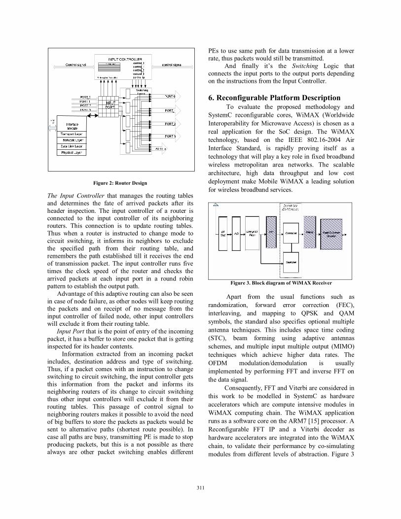
Figure 2: Router Design
The Input Controller that manages the routing tables and determines the fate of arrived packets after its header inspection. The input controller of a router is connected to the input controller of its neighboring routers. This connection is to update routing tables. Thus when a router is instructed to change mode to circuit switching, it informs its neighbors to exclude the specified path from their routing table, and remembers the path established till it receives the end of transmission packet. The input controller runs five times the clock speed of the router and checks the arrived packets at each input port in a round robin pattern to establish the output path. Advantage of this adaptive routing can also be seen in case of node failure, as other nodes will keep routing the packets and on receipt of no message from the input controller of failed node, other input controllers will exclude it from their routing table. Input Port that is the point of entry of the incoming packet, it has a buffer to store one packet that is getting inspected for its header contents. Information extracted from an incoming packet includes, destination address and type of switching. Thus, if a packet comes with an instruction to change switching to circuit switching, the input controller gets this information from the packet and informs its neighboring routers of its change to circuit switching thus other input controllers will exclude it from their routing tables. This passage of control signal to neighboring routers makes it possible to avoid the need of big buffers to store the packets as packets would be sent to alternative paths (shortest route possible). In case all paths are busy, transmitting PE is made to stop producing packets, but this is a not possible as there always are other packet switching enables different
PEs to use same path for data transmission at a lower rate, thus packets would still be transmitted. And finally it’s the Switching Logic that connects the input ports to the output ports depending on the instructions from the Input Controller. 6. Reconfigurable Platform Description To evaluate the proposed methodology and SystemC reconfigurable cores, WiMAX (Worldwide Interoperability for Microwave Access) is chosen as a real application for the SoC design. The WiMAX technology, based on the IEEE 802.16-2004 Air Interface Standard, is rapidly proving itself as a technology that will play a key role in fixed broadband wireless metropolitan area networks. The scalable architecture, high data throughput and low cost deployment make Mobile WiMAX a leading solution for wireless broadband services.
Figure 3. Block diagram of WiMAX Receiver
Apart from the usual functions such as randomization, forward error correction (FEC), interleaving, and mapping to QPSK and QAM symbols, the standard also specifies optional multiple antenna techniques. This includes space time coding (STC), beam forming using adaptive antennas schemes, and multiple input multiple output (MIMO) techniques which achieve higher data rates. The OFDM modulation/demodulation is usually implemented by performing FFT and inverse FFT on the data signal. Consequently, FFT and Viterbi are considered in this work to be modelled in SystemC as hardware accelerators which are compute intensive modules in WiMAX computing chain. The WiMAX application runs as a software core on the ARM7 [15] processor. A Reconfigurable FFT IP and a Viterbi decoder as hardware accelerators are integrated into the WiMAX chain, to validate their performance by co-simulating modules from different levels of abstraction. Figure 3
305311311
shows the block diagram of a WiMAX receiver, which includes FFT and Viterbi modules. 6.1. ARM7 Processor
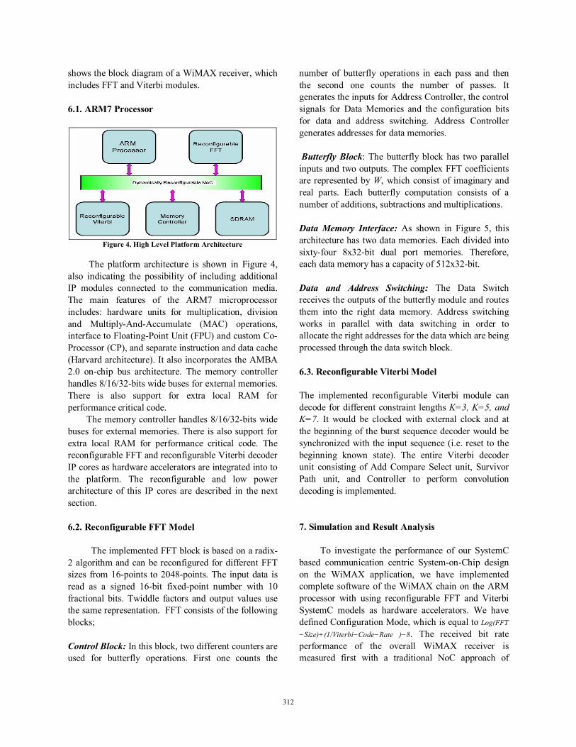
Figure 4. High Level Platform Architecture
The platform architecture is shown in Figure 4, also indicating the possibility of including additional IP modules connected to the communication media. The main features of the ARM7 microprocessor includes: hardware units for multiplication, division and Multiply-And-Accumulate (MAC) operations, interface to Floating-Point Unit (FPU) and custom Co-Processor (CP), and separate instruction and data cache (Harvard architecture). It also incorporates the AMBA 2.0 on-chip bus architecture. The memory controller handles 8/16/32-bits wide buses for external memories. There is also support for extra local RAM for performance critical code. The memory controller handles 8/16/32-bits wide buses for external memories. There is also support for extra local RAM for performance critical code. The reconfigurable FFT and reconfigurable Viterbi decoder IP cores as hardware accelerators are integrated into to the platform. The reconfigurable and low power architecture of this IP cores are described in the next section. 6.2. Reconfigurable FFT Model The implemented FFT block is based on a radix-2 algorithm and can be reconfigured for different FFT sizes from 16-points to 2048-points. The input data is read as a signed 16-bit fixed-point number with 10 fractional bits. Twiddle factors and output values use the same representation. FFT consists of the following blocks; Control Block: In this block, two different counters are used for butterfly operations. First one counts the
number of butterfly operations in each pass and then the second one counts the number of passes. It generates the inputs for Address Controller, the control signals for Data Memories and the configuration bits for data and address switching. Address Controller generates addresses for data memories. Butterfly Block: The butterfly block has two parallel inputs and two outputs. The complex FFT coefficients are represented by W, which consist of imaginary and real parts. Each butterfly computation consists of a number of additions, subtractions and multiplications. Data Memory Interface: As shown in Figure 5, this architecture has two data memories. Each divided into sixty-four 8x32-bit dual port memories. Therefore, each data memory has a capacity of 512x32-bit. Data and Address Switching: The Data Switch receives the outputs of the butterfly module and routes them into the right data memory. Address switching works in parallel with data switching in order to allocate the right addresses for the data which are being processed through the data switch block. 6.3. Reconfigurable Viterbi Model The implemented reconfigurable Viterbi module can decode for different constraint lengths K=3, K=5, and K=7. It would be clocked with external clock and at the beginning of the burst sequence decoder would be synchronized with the input sequence (i.e. reset to the beginning known state). The entire Viterbi decoder unit consisting of Add Compare Select unit, Survivor Path unit, and Controller to perform convolution decoding is implemented. 7. Simulation and Result Analysis To investigate the performance of our SystemC based communication centric System-on-Chip design on the WiMAX application, we have implemented complete software of the WiMAX chain on the ARM processor with using reconfigurable FFT and Viterbi SystemC models as hardware accelerators. We have defined Configuration Mode, which is equal to Log(FFT −Size)+(1/Viterbi−Code−Rate )−8. The received bit rate performance of the overall WiMAX receiver is measured first with a traditional NoC approach of
306312312

using wrappers and secondly with the proposed NoC with bus based interface. (See Figure 5).
0
500
1000
1500
2000
2500
3000
3500
4000
1 2 3 4 5
Configuration mode
Bitr
ate(
kbp
NoC with Wrappers Proposed NoC
Figure 5. Comparison of proposed NoC with traditional NoC
It can be seen that the proposed NoC with routers provides the same results as the traditional approach of using wrappers to integrate the components into NoC architecture. This experiment was carried out to see if there is any loss in system performance when implemented with the proposed NoC architecture. Thus, it can be concluded that the results obtained are same emphasizing the fact that the proposed NoC routers do not degrade the system performance. Increase in area of router is compensated by the reduction in design time by not having to design custom wrappers for components. To further analyze the performance of the proposed NoC architecture with traditional NoC, a network of 16 modes is simulated. The aim of this simulation is to compare the data throughput of proposed dynamically configurable NoC with bus based interface with that of traditional NoC in which the decisions about switching and packet size is made at the design time. Also wrappers are used to integrate the components. Under a moderate traffic load (with simple message passing between integrated ARM processors), data throughput is same as, both the NoCs perform the same way as they employ packet switching and the channel is shared by the data packets. However, in case of channel with high bandwidth requirement, Proposed NoC changes switching to circuit switching for that path and hence forms a dedicated path between the IPs, Packet size is also increased to allow the usage of all the available bandwidth.
25
30
35
40
45
50
55
60
65
70
30 35 40 45 50 55 60 65 70
Packet Size (%)
Thro
ughp
ut (%
)
Proposed NoC
Traditional NoC
Figure 6: comparison of data throughput vs packet size.
In case of proposed NoC, data throughput increased with the increase in packet size. To allow for the same amount of data to be transferred in same time, packet size was increased in case of shared path (traditional NoC); however, in case of packet switched network, the data throughput doesn’t increase in proportion as in case of proposed NoC (Figure 6). Data throughput increases proportional with increasing packet size as no time is wasted in switching of packets in the routers; also less time is spent on packet formation at the nodes. Thus, more data is transferred in same time. Less switching favors low power consumption as switching of packets consumes energy [14]. 8. Conclusion In this paper we have described a new approach to NoC by giving the network routers a bus based interface. Smart network stack of our previously proposed dynamically reconfigurable network on chip architecture that is optimized for Multi processor System on Chip is integrated in the network router for this purpose. The novelty of the proposed NoC lies in its ability to integrate standard non-packet based components thus reducing design time and ease of integration. A system consisting of an ARM processor, reconfigurable FFT, reconfigurable Viterbi decoder, memory controller and peripherals is considered with the option of system scalability for future upgrades. Results have demonstrated that the performance of system is unaffected by using the proposed NoC. Increase in area is compensated by the reduced design time and ease of integration. This will enable the system designers reluctant to use NoC in system to have an interface that is been used in industry for years, thus, making NoC an attractive option to consider. Simulations have also showed the effectiveness of proposed dynamically reconfigurable NoC with bus based interface with that of a traditional
307313313

NoC with fixed switching and packing size using wrappers for integration. Future work involves are and power analysis of the proposed NoC. 9. Acknowledgement The authors would like to acknowledge the support of the Engineering and Physical Sciences Council (EPSRC) of the U.K. under the grant no. EP/C528328/1. 10. References 1. Shashi Kumar, et. al, "A Network on Chip
Architecture and Design Methodology", IEEE Computer Society Annual Symposium on VLSI, Pittsburgh,Pennsylvania, USA, April 2002.
2. Pierre Guerrier, Alain Greiner, “A Generic Architecture for on-chip Packet-switched Interconnections”.
3. L. Benini, G. De Micheli, "Network on Chips: A new SoC Paradigm", IEEE computer, Jan., 2002.
4. B. Ahmad and T. Arslan, “Dynamically Reconfigurable NoC for reconfigurable MPSoC, IEEE 2005 Custom Integrated Circuits Conference, pp 277-280, 18-21 September 2005. San Jose , USA.
5. B. Ahmad, A.T. Erdogan, “Architecture of a dynamically reconfigurable NoC for adaptive Reconfigurable MPSoC”, First NASA/ESA Conference on Adpative Hardware and Systems 2006 (AHS-2006), pp. 405-411.
6. E. Rijpkema, “Trade Offs in the Design of a Router with both Guaranteed and Best-Effort Services for Networks on Chip”, In Proc. Design, Automation and Test in Europe, 2003, pp. 10350-10355.
7. C. A. Zeferino and A. A. Susin, “SoCIN: A Parametric and Scalable Network-on-Chip”, In Proc. 16th Symposium on Integrated Circuits and Systems Design, 2003, pp. 169-174.
8. M. Millberg, E. Nilsson, R. Thid, and A. Jantsch, “Guaranteed Bandwidth using Looped Containers in Temporally Disjoint Networks within the Nostrum Network on Chip”, In Proc. Design, Automation and Test in Europe, 2004, pp. 890-895.
9. F. G. Moraes, N. Laert, V. Calazans, A. V. de Mello, L. H. Mller, L. C. Ost, “HERMES: an Infrastructure for Low Area Overhead Packet-Switching
Networks on Chip”, Integration, the VLSI Journal, 38(1), pp. 69-93, Oct. 2004.
10. J. Bainbridge and S. Furber, “Chain: a Delay-Insensitive Chip Area Interconnect”, IEEE Micro, Vol. 22(5), pp. 16-23, Sept./Oct. 2002.
11.A. Lines, “Asynchronous Interconnect for Synchronous SoC Design”, IEEE Micro, Vol. 24(1), pp. 32-41, Jan./Feb. 2004.
12.E. Beigne, F. Clermidy, P. Vivet, A. Clouard, and M. Renaudin, “An Asynchronous NoC Architecture Providing Low Latency Service and its Multi-level Design Framework”, In Proc. IEEE Int’l Symposium on Asynchronous Circuits and Systems, 2005, pp. 54-63
13. F. A. Hussin, Tomokazu Yoneda and Hideo Fujiwara, “Optimization of NoC Wrapper Design under Bandwidth and Test Time Constraints”, 12 IEEE Euorpoean Test Symposium.
14. Luca Benini, Giovanni DE Micheli , “Powering Networks on Chips: Energy Efficient and Reliable interconnect design for SoCs.”
15. ARM. ARM7 TDMI Datasheet. http://www.arm.com.
308314314