
Fuzzy Timed Petri Net Definitions, Properties, and Applications
Hindawi Publishing CorporationVLSI DesignVolume 2007, Article ID 94676, 13 pagesdoi:10.1155/2007/94676
Research ArticleOnline Reconfigurable Self-Timed Links forFault Tolerant NoC
Teijo Lehtonen,1, 2 Pasi Liljeberg,2 and Juha Plosila2, 3
1 Turku Centre for Computer Science (TUCS), Joukahaisenkatu 3–5 B, 20520 Turku, Finland2 Department of Information Technology, University of Turku, 20014 Turku, Finland3 Research Council for Natural Sciences and Engineering, Academy of Finland, 00501 Helsinki, Finland
Received 15 October 2006; Accepted 4 March 2007
Recommended by Davide Bertozzi
We propose link structures for NoC that have properties for tolerating efficiently transient, intermittent, and permanent errors.This is a necessary step to be taken in order to implement reliable systems in future nanoscale technologies. The protection againsttransient errors is realized using Hamming coding and interleaving for error detection and retransmission as the recovery method.We introduce two approaches for tackling the intermittent and permanent errors. In the first approach, spare wires are introducedtogether with reconfiguration circuitry. The other approach uses time redundancy, the transmission is split into two parts, wherethe data is doubled. In both structures the presence of permanent or intermittent errors is monitored by analyzing previouserror syndromes. The links are based on self-timed signaling in which the handshake signals are protected using triple modularredundancy. We present the structures, operation, and designs for the different components of the links. The fault toleranceproperties are analyzed using a fault model containing temporary, intermittent, and permanent faults that occur both as burstsand as single faults. The results show a considerable enhancement in the fault tolerance at the cost of performance and area, andwith only a slight increase in power consumption.
Copyright © 2007 Teijo Lehtonen et al. This is an open access article distributed under the Creative Commons Attribution License,which permits unrestricted use, distribution, and reproduction in any medium, provided the original work is properly cited.
1. INTRODUCTION
The move towards nanoscale circuits increases performanceand capacities of ICs, but poses new challenges to circuit de-sign. As the dimensions shrink dramatically, it is becomingincreasingly difficult to control the variance of physical pa-rameters in the manufacturing process. This results in faultsand decreased yield which increases the costs per functioningchip [1, 2]. The yield can be maintained at an acceptable levelby admitting some amount of faults in a chip, which thenhave to be tolerated with dedicated circuit structures. Differ-ent types of errors can be tackled using a variety of fault tol-erance methods. No single method is sufficient for all typesof errors and therefore a sophisticated combination of themis needed [3].
Network-on-chip (NoC) is a structure believed to be thebasic platform of future designs [4]. In such a system thecommunication links between system modules are crucial forthe correct operation of system. In this paper, we focus onfault tolerance design of the communication links in NoC ar-chitectures. We take into consideration both the permanent
and intermittent errors that are commonly originated fromthe manufacture process or produced by electromigration aswell as transient errors caused, for example, by different noisesources and radiation.
The paper is organized as follows. In Section 2 we givebackground for the presented approach and discuss some re-lated works. The idea is presented in Section 3 followed bythe description of the created realizations in Section 4. Theresults are presented in Section 5 and in Section 6 the faulttolerance properties are analyzed. The power analysis is pre-sented in Section 7, and Section 8 contains discussion aboutthe results and possible enhancements to the design. Finallythe conclusions are presented in Section 9.
2. BACKGROUND
An NoC system consists of many processing blocks whichhave different timing requirements and can operate atdifferent clock frequencies. Communication between theseblocks needs synchronization which is error-prone. Also theclock distribution over a wide chip with low skew and jit-ter is problematic. A viable solution for this is the use of the

2 VLSI Design
Transmitter
64
req4ack4
Data
req2
ack2
nack2
reconf2
ctrl
Data
20
84
Rec
onfu
nit
44
44
44
4488 88
Rec
onfu
nit 20
84
Receiverreq2
ack2
reconf2
nack2
ctrl
Datasynd
req4
ack4
Data
reconf
64
20 7
Reconfcontrol unit
req4
ack4
req4
ack4req2, ack2, nack2, reconf2 = 2-phase control signals
req4, ack4 = 4-phase control signals
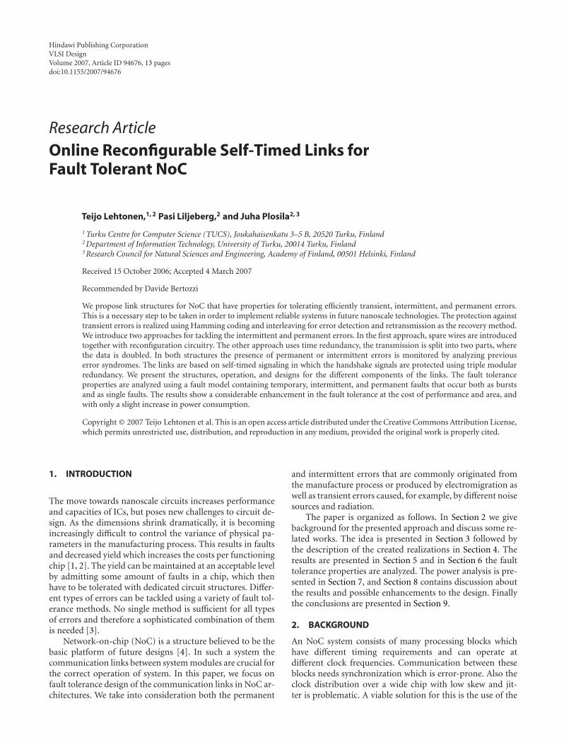
Figure 1: Simplified structure of the proposed link with spare wires and reconfiguration circuits.
globally-asynchronous locally-synchronous (GALS) designapproach, where communication between processing blocksis done asynchronously [5–7]. Therefore, we base our link onself-timed design principles [8–10].
When designing a fault tolerant on-chip link for a deepsubmicron chip, one should first consider the possible faultscenarios. The approach must be capable of tolerating mul-tiple bidirectional errors as well as burst errors [2, 11]. Fordetecting multiple bidirectional errors the Hamming code iswidely used [11–13]. The standard version of it can detecttwo single errors and with one additional check bit the er-ror detection ability can be extended to three. Cyclic codescan be used to detect burst errors [11]. Another approach forhandling burst errors is interleaving [14].
The faults can be categorized into three classes: perma-nent, intermittent, and temporary or transient faults [1].Most of the failures (80%) are caused by transient faults [4].The other way around, up to one fifth of all the failures areoriginating from permanent or intermittent faults. Thus, thefault tolerance approach must contain elements to not onlytolerate the temporary errors but also the ones of more per-manent nature. Most of the research has been concentratingon tolerating transient errors. The two methods for this pur-pose are forward error control (FEC) and automatic repeatquery (ARQ) [15], the latter of which is found to be moreenergy efficient [11]. In FEC the errors are corrected at thereceiver based on the information of the check bits while inARQ the check bits are used to detect errors and a retransmis-sion is requested when necessary. The ARQ will not work inthe presence of permanent errors and FEC with commonlyused Hamming coding loses its effectiveness already in thepresence of a single permanent fault.
Fault tolerance methods besides coding include for in-stance triple modular redundancy (TMR) and the use ofspare components together with error detection [16]. Theuse of spare wires for NoC interconnects has been presentedin [17], where the focus, however, has been on improving
yield and no method for fault detection nor reconfigurationprotocol is presented.
3. LINK STRUCTURE
The idea in this work is to combine two different fault toler-ance methods to achieve a system that is efficient in tolerat-ing transient, intermittent and permanent errors. For tran-sient faults we use Hamming coding and interleaving to de-tect faults and ARQ as the recovery method motivated byits energy efficiency as reported in [11]. For tolerating per-manent and intermittent errors we introduce two methods,one that uses hardware redundancy and the other based ontime redundancy. In the first approach spare wires are in-troduced together with reconfiguration circuits. In the sec-ond approach, the data is split into two transmissions andin both of them the transmitted data is doubled. In the re-ceiver the fault-free copy is chosen and the data of the twotransmissions are again combined into a whole word. In bothstructures, the presence of a permanent fault is detected us-ing the same Hamming code as for transient faults. A num-ber of previous error syndromes are stored and if they equal,it indicates a permanent error. The exact error location canbe determined by decoding the syndrome. A similar methodis used to switch back to the normal operation mode in thesplit transmission approach. If all the syndromes are zero forthe past transmissions, the error has probably been intermit-tent and change back to the normal mode can be carried out.
The spare wire approach aims at providing unchangedperformance in the presence of errors. However, the recon-figuration procedure is allowed to take some time since itis a rare occasion. The split transmission approach on theother hand has a significant impact on the performance andits use is motivated by considering a typical NoC system.An erroneous link could be bypassed through neighboringrouters, but this would increase traffic in other links and mayresult in congestion. Nevertheless, the total latency of links

Teijo Lehtonen et al. 3
Req
Ack
Nack
Data
(a) 2-phase bundled data
Ack
Nack
Req
0 0
1 1 1
(b) 2-phase dual rail (transmitting data “10011”)
Figure 2: Self-timed signaling.
and routers on a bypassing route set an objective to the splittransmission link design.
The width of the target link is set to 64 bits, which is splitinto four identical parts. Every part is encoded with Ham-ming (21, 16) code and the parts are interleaved. In otherwords, if we name the inputs as i0,...,63 and the check bits asc0,...,19 the coding proceeds as follows. The check bits c0, c4,c8, c12 and c16 are calculated from inputs i0, i4, i8, . . . , i60, thecheck bits c1, c5, c9, c13 and c17 are calculated from inputsi1, i5, i9, . . . , i61, and the other two interleaving sections corre-spondingly. Consequently, the system is capable of detectingerror bursts affecting up to 8 adjacent wires and at least twosimultaneous single faults extending to 8 simultaneous singlefaults if only two of them affect the same interleaving section.
In the spare wire approach, four spare wires are added tothe system, one for each interleaving section. This gives thesystem tolerance for permanent error bursts affecting up to 4wires and maximum of 4 single faults if they affect separateinterleaving sections. Thus, the total number of wires is 88,from which 64 are data, 20 check bits and 4 spares.
In the split transmission approach the data is split intotwo parts, two interleaving sections to each. The data in bothparts is doubled, preserving the interleaving. Therefore, theerror detection capability is 4-bit wide error bursts and twosingle errors. The minimum tolerance against permanent er-rors is determined by the wires located physically in the mid-dle of the link, where the two doubled parts have the min-imum physical distance to each others. Since there are fourcontrol signals between the parts (see end of the section), theminimum permanent error burst tolerance is 6 bits extend-ing up to 36 bits depending on which part of the link the er-rors affect. The minimum permanent single error toleranceis one, but a system having even 36 single errors works, if theerrors occur only in two different interleaving sections.
The timing of the data transfer between transmitter andreceiver is realized using two-phase asynchronous bundleddata signaling [10, 18], illustrated in Figure 2(a), while in-
ternally the transmitter and receiver use 4-phase signaling[10, 19]. Two-phase signaling is chosen in order to minimizethe control wire switching activity and the handshaking de-lay. This is since in the 4-phase protocol four transitions onhandshake lines, two on both request and acknowledge wires,are required, while in the 2-phase protocol only two transi-tions, one on both request and acknowledge wires, are re-quired. Hence, from this perspective 2-phase signaling proto-col is a more attractive choice for NoC interconnects, whichcould possibly have significant physical wire lengths withhigh capacitive and resistive properties [20] causing consid-erable signal delays.
Therefore, in addition to the data wires we need request(req) and acknowledgment (ack) signals to implement the2-phase signaling protocol between the transmitter and re-ceiver. For signaling the incorrectness of a data transfer fromthe receiver to transmitter we use a negative acknowledgment(nack) signal instead of ack. This makes the backward signal-ing delay-insensitive since there is no need for making tim-ing assumptions. Finally, we need also a signal for indicat-ing the reconfiguration (reconf ). The actual reconfigurationdata in the spare wire approach can be sent from receiverto transmitter serially by using self-timed dual-rail proto-col presented in Figure 2(b) [10], where ack/nack signals areused for data (0/1) and req for acknowledgement. This wayalso the reconfiguration data exchange is delay-insensitiveand no additional signals are needed.
The timing signals are crucial for the correct operationof the link and therefore, they have to be protected againsterrors. For this purpose we use triple modular redundancy(TMR) as proposed in [21]. Furthermore, the three instancesof each control signal are physically dispersed to maintain thetolerance against burst errors. The proposed link structurewith spare wires and reconfiguration circuits is presented inFigure 1.
4. REALIZATIONS
The links were designed using the Haste design language andtimeless design environment (TiDE) toolset for asynchronousdesign by Handshake Solutions [22]. Haste has support onlyfor 4-phase bundled data signaling so converter circuits werecreated to transform signaling to 2-phase and vice versa. Theconverters were designed using standard components andtranslated to structural VHDL as were also the majority vot-ers needed for TMR.
To find out the area overhead, performance penalties andthe impact on power consumption the introduced fault tol-erance causes, also a link without any fault tolerance and adesign with ARQ but no reconfiguration circuitry were real-ized. The buffering capacity of these reference designs was setto the same as in the reconfiguration cases.
4.1. Link with spare wires
The structure of the link with spare wires is presented inFigure 3. The system is pipelined to increase the throughput.The transmitter contains first a latch stage (L1), which is

4 VLSI Design
Transmitter Receiver
64
Data
req4ack4
Controlunit
req4ack4
statusreconf
Lc
84
84HL
1
L2b
L2a
Con
v2
4ph req2
ack2
nack2
reconf2
ctrl 20
Data 84
Rec
onfu
nit
V
V
V
44
4488
44
44 88
V
Rec
onfu
nit
req2
ack2
nack2
reconf2 Con
v4
2ph
20 ctrl
84 Data
req4ack4statusreconf
req4ack4
Controlunit
Lc
84
64
H
L3
64
Data
20 7
syn
dre
q4ac
k4
reco
nf
req4
ack4
Reconfcontrol unit
H = Hamming encode/decode
L1, L2a, L2b, L3, Lc = latches
req2, ack2, nack2, reconf2 =2-phase control signalsreq4, ack4 = 4-phase control signalsV =majority voter
Figure 3: Structure of the designed link with spare wires.
followed by the Hamming encoder circuitry (H). After theencoding the data with check bits is stored in one of the twoparallel output latches (L2a and L2b). These latches are usedso that while one is connected to the output channel the nextdata word can be stored to the other. When ack is receivedto indicate a correct transmission, the output latch can berapidly changed and a new transmission can begin. In thecase of negative acknowledgment (nack) the same latch staysconnected to the output channel and a retransmission is car-ried out (see also Figure 2(a)).
In the receiver the error syndrome for incoming data iscalculated and the data word is stored to a latch (L3). If thesyndrome equals zero, ack is sent and the data from the latchis forwarded to the receiver output. In the case of a nonzerosyndrome, nack is sent and the syndrome is passed to the re-configuration control unit, where it is stored into a 3-placering buffer, so that the last three nonzero syndromes arefound in this buffer. The structure and operation of the re-configuration control unit is explained in Section 4.3.
When the receiver gets a request together with the re-configuration vector from the reconfiguration control unit,it switches to the reconfiguration mode. An arbiter is usedto guarantee that the mode change cannot occur in themiddle of a receive operation. The reconfiguration data ex-change between the receiver and the transmitter is illustratedin Figure 4. The receiver sends reconf to indicate the modechange to the transmitter. The transmitter acknowledges thisthrough the req line. Next, the reconfiguration information(reconfiguration vector, 7 bits) is transferred bitwise usingack and nack lines and every bit is acknowledged with thereq line (see Figure 2(b)). After the acknowledgement of thelast bit, the receiver sends reconf to indicate the mode changeback to normal and the transmitter acknowledges it withreq. Finally, receiver sends nack, so that the transmitter sendsagain the data it was sending when the mode change tookplace.
req
req
req
req
reconf
ack/nack
reconf
nack
Tran
smit
ter
×7
Rec
eive
r
Start
Data
End
Figure 4: The protocol for sending the reconfiguration informationfrom the receiver to transmitter.
After the transmission of the control word both the re-ceiver and transmitter store the error location into the con-trol register of the correct interleaving section according tothe reconfiguration vector. The reconfiguration units werecreated using structural VHDL. The transmitter side unit isillustrated in Figure 5. Tristate buffers are used to drive thelink wires. From the control registers the exact error loca-tion is decoded using a 5-to-21 decoder. Based on that valueand the fact that no reconfiguration is done above the er-ror location and that all wires below the error location needto be reconfigured, the control signals for the tristate bufferscan be solved. By using tristate buffers instead of multiplexersthe corrupted wire can be completely isolated from the driv-ing circuit and so, for example, possible short-cuts to powerlines do not cause any power leakage. Furthermore, tristatebuffers can be easily included in the driving buffers, that are

Teijo Lehtonen et al. 5
ctrl
Decode 5 to 21 Decode 5 to 21 Decode 5 to 21 Decode 5 to 2120 5 5 5 5
21 21 21 21
i
i
i
i
i + 1
i + 1
i + 1
i + 1
Figure 5: The structure of the reconfiguration unit at the transmit-ter side.
needed to drive the capacitive on-chip wires. At the receiverside the control is realized similarly with the exception thatnow multiplexers are used to select the correct wire for eachinput.
4.2. Link with split transmission
The structure of the link with split transmission is presentedin Figures 6 and 7. The system has many similar parts to theone with spare wires. The transmitter differs after the mul-tiplexer M1. In the normal mode the output of M1 is con-nected to the output of the transmitter via the multiplexerM3. In the split mode, indicating that there is a faulty wire inthe link, the output of the transmitter is obtained from themultiplexer M2 (via M3). In the Hamming encoder circuitrythe data is split into four interleaving sections (every fourthwire per section) and the five check bits are calculated foreach section separately and interleaved. In selector Sel1 eitherfirst two or last two sections are chosen and doubled. Split-ting the data according to the interleaving sections removesthe need of two separate encoding and decoding units. Themultiplexer M2 chooses between the first and second splittransmission parts. The part is changed when ack is received,
in case of nack it stays the same and a retransmission is car-ried out.
In the receiver the error syndrome for incoming data iscalculated and the data word is stored into a latch (L3) simi-larly as in the structure with spare wires. The data and checkbits are in different parts of the data word depending onthe operation mode. This selection is not shown in Figure 6.If the transmission is correct, ack is sent to the transmit-ter and the data from the latch is forwarded to the receiveroutput via the multiplexer M5 in case of the normal modeand to the selector Sel2 in the split mode. The correctnessof the transmission is indicated in the normal mode whenthe syndrome equals zero and in the split mode when ei-ther copy of an interleaving section gives a zero-syndromefor both transmitted sections. This means that if the trans-mitted interleaving sections are marked as 1 and 2 and dou-bling creates instances a and b, the transmission is correct ifone of the following combinations have zero-syndromes: 1aand 2a, 1a and 2b, 1b and 2a, or 1b and 2b. In the case ofan incorrect transmission, nack is sent and the syndrome ispassed to the reconfiguration control unit. The syndrome ispassed to the reconfiguration control unit also during correcttransmissions in the split mode. Based on the syndromes thereconfiguration control unit detects permanent errors andcontrols the return to the normal mode if the errors havevanished (e.g., they were intermittent). The structure of thereconfiguration control unit and its operation is explained inSection 4.3.
In the split mode, the selector Sel2 separates the inter-leaved sections and using the multiplexers M4a and M4b thecorrect instances of both transmitted sections are chosen.The control for these multiplexers is obtained from the syn-dromes calculated by the decoding unit. The first split trans-mission part is stored to the latch L4 and when the secondpart arrives they are interleaved (Ilv) and passed to the out-put via M5.
If the receiver is in the normal mode and an error is de-tected (signal error from the reconfiguration control unit) itswitches to the split mode. The mode change takes place inthe same way in the split mode if the signal zero is detected.An arbiter is used to guarantee that the mode change cannotoccur in the middle of a receive operation or before a splittransmission is completed. The receiver sends reconf to in-dicate the mode change to the transmitter. The transmitteracknowledges this through the req line, after which the re-ceiver sends nack, in order to get the transmitter to resendthe data it was sending when the mode change took place.
4.3. Reconfiguration control
The reconfiguration control unit for the spare wire design isdepicted in Figure 8(a) and the unit for the split transmis-sion design in Figure 8(b). Both reconfiguration units have a3-place syndrome buffer which is divided into four 5-bit seg-ments, one segment for each interleaving section (LXa, LXband LXc, where X is the number of the segment).
In the reconfiguration control unit for the spare wire de-sign, the values of the three syndromes are compared indi-vidually in all the four segments and if they equal and are

6 VLSI Design
Transmitter Receiver
64
Data
req4ack4
Controlunit
req4ack4
statusreconf
M1
Sel1
M284 84
8484
HL1
L2a
L2b
Con
v2
4ph req2
ack2
nack2
reconf2
V
V
V
42
4284
42
42 84
V req2
ack2
nack2
reconf2 Con
v4
2ph
84
65
req4ack4statusreconf
req4ack4Control
unit
H
L3
20
Sel2
M4a
M4b
L4
Ilv
M5
M3
32
Data
64
syn
dre
q4ac
k4
Err
orZ
eroReconfiguration
control unitH = Hamming encode/decodeV =majority voter
L1, L2a, L2b, L3, L4 = latches
M1, M2, M3, M4a, M4b, M5 =multiplexersreq2, ack2, nack2, reconf2 = 2-phase control signalsreq4, ack4 = 4-phase control signals
Figure 6: Structure of the designed link with split transmission. Select and interleaver units (Sel1, Sel2, and Ilv) are presented in Figure 7.
Sel1
84...
...
...
42 42 84
42
42 42 84
42
Sel2
32
64
32
...
...
...
...
...
...
32
32
64
16
16
16
16
Ilv
16
16
16
16
...
...
...
...
...
Figure 7: Select and interleaver units.
nonzero, a signal indicating a permanent error in that inter-leaving section is asserted. Based on these signals the recon-figuration process is commenced. Since there are only onespare wire for each interleaving section, a reconfigurationstatus flag (latch Lf ) indicates if the spare has already beenused and therefore the reconfiguration cannot take place.Also arbitration between the four error signals is needed tohandle the situation, where a permanent error is detected inmany sections at the same time (e.g., a burst error).
The reconfiguration procedure creates a reconfigurationcontrol vector (latch Lrec) to be forwarded to the receiver.This contains 2-bit information indicating the correct inter-leaving section and 5 bits for pointing out the location of thecorrupted wire. The location is fetched from a ROM memoryaccording to the syndrome. In this memory, there is a placefor each of the 32 combinations of the 5-bit syndrome. Only21 of these indicate a single error. The others are set to zeroand the circuit checks if the fetched location equals zero. In
this case no reconfiguration is done, because the exact errorlocation cannot be solved.
The structure of the reconfiguration control unit for thesplit transmission design is simpler than the one explainedabove. An error is indicated via the signal error if in one of thesegments the three syndromes are equal and nonzero. Thesignal zero on the other hand is asserted if all the syndromesin all the segments are zero.
4.4. Protocol converters
Protocol converters from 2-phase to 4-phase and vice versain both spare wire and split transmission implementationsare shown in Figure 9 [6]. As mentioned earlier, 4-phase sig-naling [10, 19] is used internally in the transmitter and re-ceiver and in communication between a phase converter andthe transmitter/receiver. However, communication betweenconverters, actual communication between the transmitterand receiver, is realized by using a 2-phase handshake proto-col to minimize the number of transitions in the link controlwires [10, 18]. Hence, protocol converters are required at theboundary of the transmitter and receiver as shown in Figures3 and 6. Both spare wire and split transmission implementa-tions can utilize the same 2-to-4 and 4-to-2 phase converters.
The 4-to-2 phase converter presented in Figure 9(a) is ac-tivated by the signal req4 from the transmitter indicating thata new transaction is going to be commenced. The signal req4is connected to the clock input of both flipflops which trig-gers events in req2 and ack4. The signal req2 is the actual 2-phase request signal to the receiver indicating availability ofnew data while the 4-phase signal ack4 indicates to the trans-mitter that the data transaction has been started. Immedi-ately after the transmitter has received ack4 it sets req4 backto its original level. Observe that the direction of the eventin the 2-phase req2 signal, the actual logic signal level, is notimportant. Only the change of the signal level is monitored.After the receiver has captured the data it produced an eventin the ack2 signal, which causes ack4 to go back to its initial

Teijo Lehtonen et al. 7
synd
20
5
5
5
5
req4
ack4
7
reconf
req4
ack4
Control unit
4 7
L4c
L4a
L3c
L3a
L2c
L2a
L1c
L1a
L4b
L3b
L2b
L1b
=
=
=
=
4to
2
Syn
drom
eta
ble
32×
5
Lf Lrec
= 0
Lf = latch for flagesLrec = latch forreconfiguration vector
LXa, LXb, LXc (X = 1, . . . , 4)latches for syndromes
(a) Spare wire design
syn
d20
5 5 5 5re
q4
ack4
Err
orZ
ero
Control unit
L1a L1c L2a L2c L3a L3c L4a L4c
L1b L2b L3b L4b
= = 0 = = 0 = 0 = = 0 =
LXa, LXb, LXc (X = 1, . . . , 4) = latches for syndromes
(b) Split transmission design
Figure 8: Structures of the reconfiguration control units.
reconf2
nack2
reconf
status
D Q
DFF
CKreq4
resetRB
req2
D Q
DFF
CKRB
ack2 ack4
(a) 4-to-2 phase converter
nack2
req4
ack2
reconf2
req2
ack4
status
reconf
D QDFFCKRB
rst
D Q
DFFCKRB
rst
D QDFFCK
RBrst
(b) 2-to-4 phase converter
Figure 9: Protocol converters.

8 VLSI Design
Table 1: Comparison of the link designs, with wire delay of500 picoseconds.
Design No FT ARQ Spare Split
Latency (empty) (ns) 2.67 7.71 8.48 9.65
Latency (full) (ns) 4.93 14.98 17.82 20.31
Throughput (MWord/s) 492.6 204.5 180.5 152.7
Area ((μm)2) 6675 12 386 25 377 21 602
Transmitter 4975 8348 12 986 10 518
Receiver 1700 4038 12 391 11 083
value informing the transmitter that a new data transactioncan be started.
In the case that a retransmission is required, the receiverproduces a negative acknowledgment by asserting the signalnack2. This changes the state of status signal, indicating tothe transmitter that the same data should be resent. Eventsin the signals ack2 and nack2 are mutually exclusive, that is,there can be an event only in one of these signals as shown inFigure 2. The signal reconf2 indicates that the system entersthe reconfiguration mode and at the same time causes ack4to return to its initial state.
At the receiver side, the 2-to-4 phase converter shown inFigure 9(b), the operation is activated by an event in req2,indicating arrival of data. This initiates 4-phase handshak-ing between the converter and receiver via req4. After the re-ceiver has captured data it sets ack4, which is connected tothe clock inputs of the flipflops through logic gates. At thispoint, there are three possibilities: ack2 is sent in the case thatdata has been properly received, nack2 is sent if retransmis-sion is required (indicated by status), and if reconfigurationis going to take place reconf2 is sent (indicated by the reconfsignal) to the transmitter. Regardless of the information sentback to the transmitter, req4 is initialized back to its initialvalue which eventually resets ack4 and hence completes the4-phase handshake cycle.
5. RESULTS
The designs were mapped to a 130 nm technology, synthe-sized and simulated using specific VHDL testbenches to findout the best and worst case throughputs and latencies. Theinterconnect delay was set to 500 picoseconds, which was es-timated to model the delay between two routers in an NoCstructure including the drivers and possible repeaters. Thesame wire model was used in all simulations.
The throughputs, latencies and circuit areas are presentedin Table 1, where no FT means the reference circuit with-out any fault tolerance structure, ARQ the one with ARQ butno reconfiguration properties, spare the presented structurewith spare wires, and split is the structure with the split trans-mission properties. Latency (full) means the situation, wherethe buffer capacity of the link is totally occupied when thetransmission begins and correspondingly latency (empty)means that there is no data in the buffers. The values listed inTable 1 for the split transmission structure are measured inthe normal operation mode. The split transmission latency
Table 2: The burst error probabilities used in simulations.
Deviation px Burst length Explanation
p0 ±[0, σ) 68.3% 1 Single error
p1 ±[σ , 2σ) 27.2% 3+1 adjacent wire in
both directions
p2 ±[2σ , 3σ) 4.3% 5+2 adjacent wires in
both directions
p3 ±[3σ ,∞) 0.3% 7+3 adjacent wires in
both directions
(full) was measured to be 59.34 nanoseconds and throughput61.2 Mword/s. The reconfiguration procedure in spare wiredesign was measured to take in total 29.7 nanoseconds.
6. FAULT TOLERANCE ANALYSIS
In this section the fault tolerance abilities of the presentedlink structures are analyzed and compared against the refer-ence designs. The used fault model is extended from the onepresented in [23] to consider also burst errors as well as in-termittent and permanent errors.
According to the model presented in [23] the probabilityof error ε is given by
ε = Q(Vdd
2σN
), (1)
where Vdd is the supply voltage, σN the deviation of the noisevoltage, which is presumed to have normal distribution, andQ(x) is the Gaussian pulse defined as
Q(x) =∫∞x
1√2π
e−y2/2dy. (2)
The model assumes that a fault in a single wire is indepen-dent of the others. We extend the model by assuming that afault affects its neighbouring wires in both directions with acertain probability p1, two neighboring wires with probabil-ity p2 and so on. The probabilities used in the simulationsare obtained from the normal distribution in a way that theprobability p0 for a single error is the area under the normaldistribution curve for deviations smaller than ±σ , p1 for de-viations ±[σ , 2σ), and so forth. The probabilities used in theanalysis are presented in Table 2.
We add to the model also intermittent and permanenterrors. According to [4] 80% of all the errors are transients.We add intermittent and permanent errors respecting this re-lation and taking the view that half of the added faults areintermittent lasting 10 transmissions and the other half per-manent.
A number of test sets were generated for different valuesof σN while the Vdd was held at the constant value 1.2 V. Er-ror sets both with and without intermittent and permanenterrors were created. A test data set of one million randomdata words was generated and simulations were run on thetwo presented link structures as well as on the two referencestructures for the different error sets. The simulation resultsare shown in Figure 10.

Teijo Lehtonen et al. 9
10−6
10−5
10−4
10−3
10−2
10−1
100
Wor
der
ror
pro
babi
lity
0.1 0.12 0.14 0.16 0.18 0.2 0.22 0.24 0.26 0.28 0.3
Noise voltage deviation σN
No FTARQ
SplitSpare
(a) Error probability in the case of only transient errors
10−6
10−5
10−4
10−3
10−2
10−1
100
Wor
der
ror
pro
babi
lity
0.1 0.12 0.14 0.16 0.18 0.2 0.22 0.24 0.26 0.28 0.3
Noise voltage deviation σN
No FTARQ
SplitSpare
(b) Error probability in the case of transient, intermittent, and per-manent errors
0
50
100
150
200
250
300
350
400
450
500
Th
rou
ghp
ut(
MW
ord
/s)
0.1 0.12 0.14 0.16 0.18 0.2 0.22 0.24 0.26 0.28 0.3
Noise voltage deviation σN
No FTARQ
SplitSpare
(c) Throughput in the case of only transient errors
0
50
100
150
200
250
300
350
400
450
500
Th
rou
ghp
ut(
MW
ord
/s)
0.1 0.12 0.14 0.16 0.18 0.2 0.22 0.24 0.26 0.28 0.3
Noise voltage deviation σN
No FTARQ
SplitSpare
(d) Throughput in the case of transient, intermittent, and perma-nent errors
Figure 10: The performance of different structures in the presence of different error scenarios.
The word error probability as a function of the noise volt-age deviation is shown in Figure 10(a) for the error modelwithout intermittent and transient errors. The fault toleranceproperties of the two presented structures match with the ref-erence circuit with ARQ but no reconfiguration. This is quiteobvious since the fault tolerance method they use is the same.Quite obvious is also the fact, that the structure without anyfault tolerance properties results in a higher word error prob-ability rate as the others.
The corresponding throughputs are shown in Fig-ure 10(c). We see that the throughput decreases as the noise
deviation increases for all the other structures except for theone without fault tolerance properties, which have constantthroughput regardless of the amount of faults. The ARQ isrealized in a way that in the case of a detected fault, the wordis retransmitted once, but no more. If there was no limit forthe number of retransmissions the circuit would end up in alivelock. The effect of most transient faults, for example, in-tersymbol interference, radiation induced pulses, crosstalk,and so forth, ceases by just waiting before sampling the val-ues on the line. For this reason the number of retransmis-sions is limited to one. Unfortunately, our error model does

10 VLSI Design
Table 3: Energy consumption analysis of the link designs.
(a) Energy per transmission for σ = 0.10
Design No FT ARQ Spare Split
Transmitter (pJ) 26.28 28.31 29.50 30.94
Receiver (pJ) 7.12 12.42 14.46 17.75
Total (pJ) 33.41 40.74 43.96 48.69
Compared to ARQ +7.9% +19.5%
(b) Energy per transmission for σ = 0.20
Design No FT ARQ Spare Split
Transmitter (pJ) 26.28 28.98 29.57 34.25
Receiver (pJ) 7.80 21.24 16.30 46.37
Total (pJ) 34.08 50.22 45.86 80.62
Compared to ARQ −8.7% +60.5%
not take into account this phenomenon but instead all trans-fers are presumed to be independent of each others. Thisgives pessimistic values for the fault tolerance of the simu-lated structures. Nevertheless, they can be compared with theused model since the situation is the same for all of them.The impact of the limited number of retransmissions is seenin the saturation of the throughputs as the noise voltage de-viation is increased. The throughput-based ranking order ofthe structures corresponds to the values presented in Table 1and it remains the same for all the simulated sets.
The simulation results for the error sets with also inter-mittent and permanent errors are shown in Figures 10(b)and 10(d). The reference structures lose their operabilityrapidly as the noise voltage deviation is increased. As ex-pected, they do not work in the presence of permanentfaults. The presented online reconfigurable structures main-tain their operability although there is more variance in theresults. The variance is originated from the randomness ofthe error locations and the properties of the structures toguarantee tolerance against some limited set of permanentfaults while a larger set is tolerated with some conditions.From the two presented structures the one with split trans-mission shows higher fault tolerance.
The throughputs presented in Figure 10(d) show similarchanges as in the simulations without intermittent and per-manent faults. For the reference structure without fault toler-ance, the throughput is constant and for the reference struc-ture with ARQ the throughput decreases, now more rapidlythan without intermittent and permanent faults, and satu-rates because of the limited number of retransmissions. Thespare wire approach has exceptions to this trend. When thereconfiguration has been successfully carried out, the perma-nently faulty wires have been replaced by spares, the through-put equals the fault-free situation and the word error proba-bility remains low. On the other hand, if the reconfigurationis not successful the fault tolerance is almost as low as for
0
10
20
30
40
50
60
70
80
En
ergy
per
tran
smis
sion
(pJ)
No FT ARQ Spare Split
TransmitterRecevier
Figure 11: Energy consumption analysis of the link designs.
the reference circuit with ARQ, and the throughput has sim-ilar values as in the case without intermittent and permanentfaults for high noise voltage deviation. The split transmis-sion structure shows a similar curve to the one in the casewithout intermittent and permanent faults, but with inter-mittent and permanent faults it saturates to a lower through-put value. This is because the throughput in the split modeis lower and in the presence of a permanent fault, the circuitremains in the split transmission mode all the time.
7. POWER ANALYSIS
The power consumption of the systems was analyzed by us-ing Synopsys Primepower. Simulations were carried out foran input set of ten thousand random words for two differenterror sets containing transient, intermittent, and permanenterrors. The error sets with noise voltage deviations σ = 0.10and σ = 0.20 were chosen. The first one demonstrates a sit-uation of low error probability whereas the second containsa lot of errors. By comparing these two analyses the powerefficiency in the presence of errors can be seen. The simula-tion results are presented in Table 3 and in Figure 11, whereno FT means the reference circuit without any fault tolerancestructures, ARQ the one with ARQ but no reconfigurationproperties, spare the presented structure with spare wires,and split is the structure with the split transmission proper-ties. The average power consumption is translated to energyconsumption per transmitted word by taking into consider-ation the throughputs of the different systems and averagingover the random input set.
The energy consumption values do not include the en-ergy taken by the drivers driving the link wires. These val-ues were not included since the main target of the analysisis to see the impact of the added reconfiguration propertiesin comparison to the reference circuit with ARQ but no re-configuration. These values are comparable since in all of

Teijo Lehtonen et al. 11
these systems the number of active wires is the same or thedifference in the wire count can be ignored. In the spare wireapproach, the added spare wires do not consume any powerand therefore, the number of active data wires is 84 as is thecase in the split and reference designs. In the systems with re-configuration properties, there is one additional tripled con-trol signal (reconf2), but it is switched extremely rarely. Thepower analysis of the majority voters indicates that the powerconsumption of the majority voters connected to the reconf2signals is less than one thousandth of the corresponding val-ues of the ones connected to the ack2 signals. The relativedifferences of the energy consumptions of the spare and splitapproaches as compared to the reference with only ARQ arepresented in Table 3 for the both simulated noise voltage de-viations.
The results indicate that the addition of reconfigurationproperties results in a small increase in power consumption.For the spare wire approach the increase is less than 8% inthe case of few errors, as for the split transmission designthe increase is almost 20%. When the noise voltage deviationis increased the values show dramatical but nevertheless ex-pectable results. Now the spare wire approach gives the bestpower consumption values, almost 9% less than for the ref-erence design. The reasons for this were already discussed inthe previous section. The power consumption of the sparewire approach is almost the same as without any permanentor intermittent errors when the reconfiguration is successful.The split transmission design uses a lot more energy than theothers, which is rather obvious since it takes many transmis-sion for all the words.
From the power consumption simulations it can be con-cluded that the spare wire approach is more power efficientthan the split transmission approach, and that the addition ofspare wires and the needed reconfiguration properties doesnot cause any considerable changes in the power consump-tion.
On the other hand, the results also indicate that the addi-tion of fault tolerance properties in general results in a higherpower consumption. This observation is further strength-ened by the fact that the system without fault tolerance prop-erties contains less wires than the others.
8. DISCUSSION
When comparing the designs with the reconfiguration prop-erties to the ARQ design without them, it can be noticed thatthere is a performance penalty. In the spare wire design, thelatency increases 10%/19% (empty/full) and the throughputdecreases 12%, while in the split transmission design the la-tency increase is 25%/36% and the throughput decrease 25%.Thus, the spare wire approach has a smaller impact on theperformance. On the other hand, the area overhead is largerin the spare wire approach. It uses 105% more area thanthe ARQ design without reconfiguration. The correspondingvalue for the split transmission is 75%. The area increase ismainly due to the reconfiguration control unit in the receiver.Moreover, the reconfiguration logic in both the transmitterand receiver consume area.
The split transmission performance should be com-pared to the situation, where the erroneous link is bypassedthrough neighbouring links and routers in an NoC. Thesplit transmission latency (full) is 14.4 nanoseconds largerthan three times the latency of the reference circuit withoutsplit transmission properties. The three link latencies cor-responds to the shortest route to bypass a link in a mesh-shaped NoC. In addition to the link latencies, the latenciesof the two routers contribute to the total delay of the bypassroute. The latency of these two routers is comparable to the14.4 nanoseconds. Therefore, the latency of the split trans-mission is approximately the same as that of bypassing theerroneous link. The essential difference is that bypassing in-creases traffic in neighbouring links and may cause seriousconsequences in the form of congestion. In the worst casethis affects the operation of the whole NoC.
The area overhead should be considered in the NoC con-text. Let us consider a simple mesh structure, where onerouter is assigned for each resource and the size of a resourceis two times two millimeters [24]. There are three bidirec-tional links per each resource, thus, in total six transmit-ter/receiver pairs per resource. The area overhead caused bythe introduced fault tolerance is only 2.2%–2.8% comparedto the situation without any fault tolerance. The router areawas not included in this calculation but it further decreasesthe relative area overhead.
If the link is connected, for example, between NoCrouters, the buffering capacity of the link can be taken intoaccount, and so the buffering capacity of the routers can bedecreased by the same amount. This obviously reduces thearea overhead. In the same way the tristate buffers of thetransmitter reconfiguration unit in the spare wire approachcan be a part of the link drivers as was already discussed inSection 4.1.
The simulations were carried out using a 130 nm tech-nology. As the dimensions have been scaled below 100 nmthe delay of wires has not decreased as is the case with thedelay of logic. The gap between the wire and logic delays isexpected to increase as scaling deeper into nano regime [4].Based on this scenario and because the bottleneck at the mo-ment are the receiver and transmitter units, the performanceof the presented link structures should increase as the dimen-sions are scaled down.
The main parts were created using a modelling languageand synthesis tools which use a rather conservative approachto the problem. Based on our previous experience we pre-dict that the performance could be significantly enhanced bycareful manual design although still using standard gate li-braries [6].
In the presented designs the approach for transient faulttolerance was the use of error detection and ARQ with stop-and-wait strategy. The addition of reconfiguration to tackleintermittent and permanent errors does not force sticking atthis approach. Quite as well forward error correction and inthe spare wire approach also different ARQ strategies [15]could be used. One such strategy is go-back-N , where insteadof waiting for an acknowledgment of correct transfer, thetransmission proceeds with next word instanteously and in

12 VLSI Design
the case of an error the system returns the necessary amountof words (N) backwards. Another strategy is selective repeat,where the transmission is continued as in go-back-N , but inthe presence of an error only the erroneous word is asked tobe retransmitted. In the presented analysis the focus has beenon the comparison of the reconfigurable structures with thereference structure with ARQ but no reconfiguration. Sinceall these designs use the same ARQ strategy, the choice of ithas not been of vital importance and hence, the simplest onehas been used.
The reconfiguration control indicates a permanent er-ror when the same error syndrome has been repeated threetimes. In the split transmission approach the reconfigura-tion could be advantageous also under other conditions. InFigure 10(a), we see a slightly smaller error probability forsplit transmission than for the other designs when σN = 0.30.In this case the circuit has entered the split transmissionmode since the temporary error probability has been so largethat the same error syndrome has been repeated three times.The lower throughput for this situation confirms the diag-nosis. This gives an idea that the change to the split trans-mission mode might be advantageous if the error occurrencerate crosses some limit.
The tolerance against single permanent faults in the splittransmission design is limited by the fixed location of thedoubled data parts. If the location of the permanent faultwas more exactly isolated, the placement of the doubled datacould be controlled and a greatly improved tolerance againstsingle faults could be achieved. The error location could bedetermined using the syndromes as is done in the spare wiredesign. This would probably increase the control logic andwould also result in performance degradation. The presentedapproach has the assumption that if there are multiple errors,they most likely occur as bursts, which can be motivated byconsidering different manufacture defects.
The split transmission design has a property to returnto the normal mode if the fault was intermittent. A simi-lar property would be advantageous also to the spare wiredesign, where the reconfiguration at the moment is irre-versible. The circuit is not able to tolerate permanent errorsif there have been intermittent errors in the same interleav-ing section (but at a different wire) although the intermittentfault has vanished. The intermittent faults in practice repeatthemselves in the same locations due to, for example, smallanomalies in the manufactured chip, which turn into faultsunder certain environmental conditions. However, the usedfault model considers all the intermittent faults independentof each others and therefore gives pessimistic values for thefault tolerance properties of the spare wire approach. The ad-vanced detection of different fault scenarios will be a part ofour future research.
The number of spare wires in the presented design wasset to four and they were assigned one for each interleavingsection. The fault tolerance properties could be enhanced byincreasing the number of spare wires. It would also be ad-vantageous to have the spare wires assigned more flexibly todifferent interleaving sections. One interleaving section mayhave many erroneous wires while some other has none. The
drawback of the increased flexibility is the growth of com-plexity which probably leads to a performance decrease andarea overhead.
In this work, the transmitter and receiver circuits werepresumed error-free. When considering fault tolerance of fu-ture nanoscale systems, also these circuits should be takeninto consideration from the fault tolerance perspective. Wewill address this issue as a part of our future work.
9. CONCLUSION
We proposed link structures that have properties for tolerat-ing efficiently transient, intermittent, and permanent errors.The protection against transient errors was realized usingHamming coding and interleaving for error detection andARQ as the recovery method. Two approaches were intro-duced to tackle the intermittent and permanent errors. Splittransmission was an approach utilizing time redundancywhile the other structure, which introduced spare wires, wasa hardware redundancy approach. Communication in thelinks was based on asynchronous 2-phase signaling and thecontrol signals for ARQ and reconfiguration were incorpo-rated into these control signals. The control lines were pro-tected using triple modular redundancy.
We presented designs for the different components of thelinks and proposed the needed reconfiguration control. Thedesigns were implemented, simulated and compared againstreference designs. The simulation results show that the per-formance decrease when comparing to a design with ARQbut no reconfiguration is larger for the split transmission de-sign (latency 31%/throughput 25%) than for the spare wiredesign (15%/10%) while the area overhead is larger for thespare wire design (105%) as for the split transmission design(75%). The fault tolerance analysis using error models con-taining temporary, intermittent, and permanent faults thatoccur as both bursts and single errors, shows the effectivenessof the presented link structures. When there are no intermit-tent or permanent errors present, the structures perform thesame way as the reference design with ARQ but no recon-figuration, and which clearly outperforms the reference de-sign without any fault tolerance. When also intermittent andpermanent errors are taken into account, the presented linkstructures show clearly better results than the reference de-signs. From the two presented reconfiguration structures, thesplit transmission design tolerates faults slightly better thanthe design with four spare wires. On the other hand, the sparewire approach turned out to be more power efficient thanthe split transmission design. Using the spare wire design thepower consumption is approximately the same as with thereference design with ARQ but no reconfiguration. In thepresence of an excessive amount of errors the spare wire ap-proach turns out to be even more energy efficient than thereference design.
Our research shows that combining different fault toler-ance methods a structure capable of tolerating all differenttypes of errors is achievable. As is always the case with faulttolerance, this does not come for free. There is a clear areaoverhead, but on the other hand when comparing to the IP

Teijo Lehtonen et al. 13
block areas in the NoC context, the overhead is only a coupleof percents.
ACKNOWLEDGMENTS
The authors would like to thank The Finnish Cultural Foun-dation, The Foundation of Technology, and Ulla TuominenFoundation for their financial support. They also acknowl-edge the financial support from Academy of Finland.
REFERENCES
[1] C. Constantinescu, “Trends and challenges in VLSI circuit re-liability,” IEEE Micro, vol. 23, no. 4, pp. 14–19, 2003.
[2] International Technology Roadmap for Semiconductors,2005, http://public.itrs.net/.
[3] T. Lehtonen, J. Plosila, and J. Isoaho, “On fault tolerancetechniques towards nanoscale circuits and systems,” Tech.Rep. 708, Turku Centre for Computer Science (TUCS), Turku,Finland, August 2005.
[4] G. De Micheli and L. Benini, Networks on Chips, Morgan Kauf-mann Publishers, San Francisco, Calif, USA, 2006.
[5] D. M. Chapiro, Globally-asynchronous locally-synchronous sys-tems, Ph.D. thesis, Stanford University, Stanford, Calif, USA,October 1984.
[6] P. Liljeberg, J. Plosila, and J. Isoaho, “Self-timed communi-cation platform for implementing high-performance systems-on-chip,” Integration, the VLSI Journal, vol. 38, no. 1, pp. 43–67, 2004.
[7] J. Muttersbach, T. Villiger, and W. Fichtner, “Practical de-sign of globally-asynchronous locally-synchronous systems,”in Proceedings of the 6th International Symposium on AdvancedResearch in Asynchronous Circuits and Systems (ASYNC ’00),pp. 52–59, Eilat, Israel, April 2000.
[8] M. Renaudin, “Asynchronous circuits and systems: a promis-ing design alternative,” Microelectronic Engineering, vol. 54,no. 1-2, pp. 133–149, 2000.
[9] C. L. Seitz, “System timing,” in Introduction to VLSI Systems, C.Mead and L. Conway, Eds., chapter 7, Addison-Wesley, Read-ing, Mass, USA, 1980.
[10] J. Sparsø and S. Furber, Priciples of Asynchronous CircuitDesign—A System Perspective, Kluwer Academic Publishers,Dordrecht, The Netherlands, 2001.
[11] D. Bertozzi, L. Benini, and G. De Micheli, “Error con-trol schemes for on-chip communication links: the energy-reliability tradeoff,” IEEE Transactions on Computer-Aided De-sign of Integrated Circuits and Systems, vol. 24, no. 6, pp. 818–831, 2005.
[12] S. R. Sridhara and N. R. Shanbhag, “Coding for system-on-chip networks: a unified framework,” IEEE Transactions onVery Large Scale Integration (VLSI) Systems, vol. 13, no. 6, pp.655–667, 2005.
[13] L. Li, N. Vijaykrishnan, M. Kandemir, and M. J. Irwin, “Adap-tive error protection for energy efficiency,” in Proceedings ofIEEE/ACM International Conference on Computer-Aided De-sign (ICCAD ’03), pp. 2–7, San Jose, Calif, USA, November2003.
[14] H. Zimmer and A. Jantsch, “A fault model notation and error-control scheme for switch-to-switch buses in a network-on-chip,” in Proceedings of the 1st IEEE/ACM/IFIP InternationalConference on Hardware/Software Codesign and System Syn-thesis (CODES+ISSS ’03), pp. 188–193, Newport Beach, Calif,USA, October 2003.
[15] R. E. Ziemer and R. L. Peterson, Introduction to DigitalCommunication, Prentice-Hall, Upper Saddle River, NJ, USA,2nd edition, 2001.
[16] B. W. Johnson, Design and Analysis of Fault-Tolerant DigitalSystems, Addison-Wesley, Reading, Mass, USA, 1989.
[17] C. Grecu, A. Ivanov, R. Saleh, and P. P. Pande, “NoC inter-connect yield improvement using crosspoint redundancy,” inProceedings of the 21st IEEE International Symposium on Defectand Fault Tolerance in VLSI Systems (DFT ’06), pp. 457–465,Arlington, Va, USA, October 2006.
[18] I. E. Sutherland, “Micropipelines,” Communications of theACM, vol. 32, no. 6, pp. 720–738, 1989, The 1988 TuringAward Lecture.
[19] A. Davis and S. M. Nowick, “Asynchronous circuit design:motivation, background and methods,” in Asynchronous Dig-ital Circuit Design, G. Birtwistle and A. Davis, Eds., pp. 1–49,Springer, New York, NY, USA, 1995.
[20] W. J. Dally and J. W. Poulton, Digital Systems Engineering,Cambridge University Press, Cambridge, UK, 1998.
[21] S. Murali, T. Theocharides, N. Vijaykrishnan, M. J. Irwin, L.Benini, and G. De Micheli, “Analysis of error recovery schemesfor networks on chips,” IEEE Design & Test of Computers,vol. 22, no. 5, pp. 434–442, 2005.
[22] Handshake Solutions, http://www.handshakesolutions.com/.[23] R. Hegde and N. R. Shanbhag, “Toward achieving energy effi-
ciency in presence of deep submicron noise,” IEEE Transac-tions on Very Large Scale Integration (VLSI) Systems, vol. 8,no. 4, pp. 379–391, 2000.
[24] W. J. Dally and B. Towles, “Route packets, not wires: on-chipinterconnection networks,” in Proceedings of the 38th DesignAutomation Conference, pp. 684–689, Las Vegas, Nev, USA,June 2001.

Submit your manuscripts athttp://www.hindawi.com
VLSI Design
Hindawi Publishing Corporationhttp://www.hindawi.com Volume 2014
International Journal of
RotatingMachinery
Hindawi Publishing Corporationhttp://www.hindawi.com Volume 2014
Hindawi Publishing Corporation http://www.hindawi.com
Journal ofEngineeringVolume 2014
Hindawi Publishing Corporationhttp://www.hindawi.com Volume 2014
Shock and Vibration
Hindawi Publishing Corporationhttp://www.hindawi.com Volume 2014
Mechanical Engineering
Advances in
Hindawi Publishing Corporationhttp://www.hindawi.com Volume 2014
Civil EngineeringAdvances in
Acoustics and VibrationAdvances in
Hindawi Publishing Corporationhttp://www.hindawi.com Volume 2014
Hindawi Publishing Corporationhttp://www.hindawi.com Volume 2014
Electrical and Computer Engineering
Journal of
Hindawi Publishing Corporationhttp://www.hindawi.com Volume 2014
Distributed Sensor Networks
International Journal of
The Scientific World JournalHindawi Publishing Corporation http://www.hindawi.com Volume 2014
SensorsJournal of
Hindawi Publishing Corporationhttp://www.hindawi.com Volume 2014
Modelling & Simulation in EngineeringHindawi Publishing Corporation http://www.hindawi.com Volume 2014
Hindawi Publishing Corporationhttp://www.hindawi.com Volume 2014
Active and Passive Electronic Components
Hindawi Publishing Corporationhttp://www.hindawi.com Volume 2014
Chemical EngineeringInternational Journal of
Control Scienceand Engineering
Journal of
Hindawi Publishing Corporationhttp://www.hindawi.com Volume 2014
Antennas andPropagation
International Journal of
Hindawi Publishing Corporationhttp://www.hindawi.com Volume 2014
Hindawi Publishing Corporationhttp://www.hindawi.com Volume 2014
Navigation and Observation
International Journal of
Advances inOptoElectronics
Hindawi Publishing Corporation http://www.hindawi.com
Volume 2014
RoboticsJournal of
Hindawi Publishing Corporationhttp://www.hindawi.com Volume 2014
Copyright © 2022 FDOKUMEN