DRV8805 Unipolar Stepper Motor Driver IC datasheet (Rev. D)
29
8.2V to 60V DRV8805 Quad Low-Side Driver Fault Protection Controller 1 A M + – + – Clamp Diodes 5 RESET nFAULT 1 A 1 A 1 A STEP/DIR Product Folder Sample & Buy Technical Documents Tools & Software Support & Community An IMPORTANT NOTICE at the end of this data sheet addresses availability, warranty, changes, use in safety-critical applications, intellectual property matters and other important disclaimers. PRODUCTION DATA. DRV8805 SLVSAW3D – JULY 2011 – REVISED JANUARY 2016 DRV8805 Unipolar Stepper Motor Driver IC 1 1 Features 1• 4-Channel Protected Low-Side Driver – Four NMOS FETs With Overcurrent Protection – Integrated Inductive Clamp Diodes • Indexer/Translator for Unipolar Stepper Motors – Simple Step/Direction Interface – Three Step Modes (2-Phase Full-Step, 1-2- Phase Half-Step, 1-Phase Wave Drive) • DW Package: 1.5-A (Single Channel On) / 800-mA (Four Channels On) Maximum Drive Current per Channel (at 25°C) • PWP Package: 2-A (Single Channel On) / 1-A (Four Channels On) Maximum Drive Current per Channel (at 25°C, With Proper PCB Heatsinking) • 8.2-V to 60-V Operating Supply Voltage Range • Thermally Enhanced Surface Mount Package 2 Applications • Gaming Machines • General Unipolar Stepper Motor Drivers 3 Description The DRV8805 provides an integrated solution for driving unipolar stepper motors. It includes four low- side drivers with overcurrent protection and provides built-in diodes to clamp turnoff transients generated by the motor windings. Indexer logic to control a unipolar stepper motor using a simple step/direction interface is also integrated. Three stepping modes are supported: 2 phase (full-step), 1-2 phase (half-step), and 1-phase (wave drive). In the SOIC (DW) package, the DRV8805 can supply up to 1.5-A (one channel on) or 800-mA (all channels on) continuous output current per channel, at 25°C. In the HTSSOP (PWP) package, it can supply up to 2-A (one channel on) or 1-A (four channels on) continuous output current per channel, at 25°C with proper PCB heatsinking. Internal shutdown functions are provided for overcurrent protection, short-circuit protection, under voltage lockout, and overtemperature, and faults are indicated by a fault output pin. The DRV8805 is available in a 20-pin thermally- enhanced SOIC package and a 16-pin HTSSOP package (Eco-friendly: RoHS & no Sb/Br). Device Information (1) PART NUMBER PACKAGE BODY SIZE (NOM) DRV8805 SOIC (20) 12.80 mm × 7.50 mm HTSSOP (16) 5.00 mm × 4.40 mm (1) For all available packages, see the orderable addendum at the end of the data sheet. Simplified Schematic
-
Upload
khangminh22 -
Category
Documents
-
view
3 -
download
0
Transcript of DRV8805 Unipolar Stepper Motor Driver IC datasheet (Rev. D)

8.2V to 60V
DRV8805Quad
Low-Side Driver
Fault Protection
Controller
1 A
M
+ ±
+ ±
ClampDiodes
5
RESET
nFAULT
1 A
1 A
1 A
STEP/DIR
Product
Folder
Sample &Buy
Technical
Documents
Tools &
Software
Support &Community
An IMPORTANT NOTICE at the end of this data sheet addresses availability, warranty, changes, use in safety-critical applications,intellectual property matters and other important disclaimers. PRODUCTION DATA.
DRV8805SLVSAW3D –JULY 2011–REVISED JANUARY 2016
DRV8805 Unipolar Stepper Motor Driver IC
1
1 Features1• 4-Channel Protected Low-Side Driver
– Four NMOS FETs With Overcurrent Protection– Integrated Inductive Clamp Diodes
• Indexer/Translator for Unipolar Stepper Motors– Simple Step/Direction Interface– Three Step Modes (2-Phase Full-Step, 1-2-
Phase Half-Step, 1-Phase Wave Drive)• DW Package: 1.5-A (Single Channel On) /
800-mA (Four Channels On) Maximum DriveCurrent per Channel (at 25°C)
• PWP Package: 2-A (Single Channel On) /1-A (Four Channels On) Maximum Drive Currentper Channel (at 25°C, With Proper PCBHeatsinking)
• 8.2-V to 60-V Operating Supply Voltage Range• Thermally Enhanced Surface Mount Package
2 Applications• Gaming Machines• General Unipolar Stepper Motor Drivers
3 DescriptionThe DRV8805 provides an integrated solution fordriving unipolar stepper motors. It includes four low-side drivers with overcurrent protection and providesbuilt-in diodes to clamp turnoff transients generatedby the motor windings.
Indexer logic to control a unipolar stepper motorusing a simple step/direction interface is alsointegrated. Three stepping modes are supported: 2phase (full-step), 1-2 phase (half-step), and 1-phase(wave drive).
In the SOIC (DW) package, the DRV8805 can supplyup to 1.5-A (one channel on) or 800-mA (all channelson) continuous output current per channel, at 25°C. Inthe HTSSOP (PWP) package, it can supply up to 2-A(one channel on) or 1-A (four channels on)continuous output current per channel, at 25°C withproper PCB heatsinking.
Internal shutdown functions are provided forovercurrent protection, short-circuit protection, undervoltage lockout, and overtemperature, and faults areindicated by a fault output pin.
The DRV8805 is available in a 20-pin thermally-enhanced SOIC package and a 16-pin HTSSOPpackage (Eco-friendly: RoHS & no Sb/Br).
Device Information(1)
PART NUMBER PACKAGE BODY SIZE (NOM)
DRV8805SOIC (20) 12.80 mm × 7.50 mmHTSSOP (16) 5.00 mm × 4.40 mm
(1) For all available packages, see the orderable addendum atthe end of the data sheet.
Simplified Schematic

2
DRV8805SLVSAW3D –JULY 2011–REVISED JANUARY 2016 www.ti.com
Product Folder Links: DRV8805
Submit Documentation Feedback Copyright © 2011–2016, Texas Instruments Incorporated
Table of Contents1 Features .................................................................. 12 Applications ........................................................... 13 Description ............................................................. 14 Revision History..................................................... 25 Pin Configuration and Functions ......................... 36 Specifications......................................................... 4
6.1 Absolute Maximum Ratings ...................................... 46.2 ESD Ratings.............................................................. 46.3 Recommended Operating Conditions....................... 46.4 Thermal Information .................................................. 56.5 Electrical Characteristics........................................... 56.6 Timing Requirements ................................................ 66.7 Typical Characteristics .............................................. 7
7 Detailed Description .............................................. 87.1 Overview ................................................................... 87.2 Functional Block Diagram ......................................... 87.3 Feature Description................................................... 9
7.4 Device Functional Modes........................................ 108 Application and Implementation ........................ 12
8.1 Application Information............................................ 128.2 Typical Application .................................................. 12
9 Power Supply Recommendations ...................... 149.1 Bulk Capacitance .................................................... 14
10 Layout................................................................... 1510.1 Layout Guidelines ................................................. 1510.2 Layout Example .................................................... 1510.3 Thermal Considerations ........................................ 15
11 Device and Documentation Support ................. 1711.1 Documentation Support ....................................... 1711.2 Trademarks ........................................................... 1711.3 Electrostatic Discharge Caution............................ 1711.4 Glossary ................................................................ 17
12 Mechanical, Packaging, and OrderableInformation ........................................................... 17
4 Revision HistoryNOTE: Page numbers for previous revisions may differ from page numbers in the current version.
Changes from Revision C (March 2012) to Revision D Page
• Changed Catch Diodes to Clamp Diodes in Features .......................................................................................................... 1• Added ESD Ratings table, Feature Description section, Device Functional Modes, Application and Implementation
section, Power Supply Recommendations section, Layout section, Device and Documentation Support section, andMechanical, Packaging, and Orderable Information section ................................................................................................. 1
• Updated the text in the EXTERNAL COMPONENTS OR CONNECTIONS column for nHOME row .................................. 3• Updated PARAMETERS, TEST CONDTIONS, MIN, TYP, and MAX values in the nHOME OUTPUT section in the
Electrical Characteristics table ............................................................................................................................................... 5

1
2
3
4
5
6
7
8
9
10
14
13
12
11
15
16
17
18
19
20 nFAULT
nHOME
STEP
DIR
GND
GND
GND
SM0
SM1
RESET
OUT4
nENBL
GND
OUT3
GND
GND
OUT1
OUT2
VM
VCLAMP1
2
3
4
5
6
7
8
10
9
11
12
13
14
15
16 nFAULT
nHOME
STEP
DIR
GND
SM0
SM1
RESETnENBL
OUT3
OUT4
GND
OUT1
OUT2
VM
VCLAMP
GND
3
DRV8805www.ti.com SLVSAW3D –JULY 2011–REVISED JANUARY 2016
Product Folder Links: DRV8805
Submit Documentation FeedbackCopyright © 2011–2016, Texas Instruments Incorporated
5 Pin Configuration and Functions
DW Package20-Pin Wide SOIC
Top ViewPWP Package
16-Pin HTSSOPTop View
(1) Directions: I = input, O = output, OD = open-drain output
Pin FunctionsPIN
I/O (1) DESCRIPTION EXTERNAL COMPONENTSOR CONNECTIONSNAME SOIC HTSSOP
POWER AND GROUND
GND 5, 6, 7,14, 15, 16
5, 12,PPAD — Device ground All pins must be connected to GND.
VM 1 1 — Device power supply Connect to motor supply (8.2 V to 60 V).CONTROL
DIR 17 13 I Direction input Level controls direction of rotation – internalpulldown
nENBL 10 8 I Enable input Active low enables outputs – internal pulldown
RESET 11 9 I Reset input Active-high reset input initializes internallogic – internal pulldown
SM0 13 11I Step mode Sets step mode – see step modes section for
details – internal pulldownsSM1 12 10
STEP 18 14 I Step input Rising edge advances motor to next step –internal pulldown
STATUS
nFAULT 20 16 OD Fault Logic low when in fault condition (overtemp,overcurrent)
nHOME 19 15 OD Home Logic low when indexer is at home position –push-pull structure
OUTPUTOUT1 3 3 O Output 1 Connect to load 1OUT2 4 4 O Output 2 Connect to load 2OUT3 8 6 O Output 3 Connect to load 3OUT4 9 7 O Output 4 Connect to load 4
VCLAMP 2 2 — Output clamp voltage Connect to VM supply, or Zener diode to VMsupply

4
DRV8805SLVSAW3D –JULY 2011–REVISED JANUARY 2016 www.ti.com
Product Folder Links: DRV8805
Submit Documentation Feedback Copyright © 2011–2016, Texas Instruments Incorporated
(1) Stresses beyond those listed under Absolute Maximum Ratings may cause permanent damage to the device. These are stress ratingsonly, which do not imply functional operation of the device at these or any other conditions beyond those indicated under RecommendedOperating Conditions. Exposure to absolute-maximum-rated conditions for extended periods may affect device reliability.
(2) All voltage values are with respect to network ground terminal.
6 Specifications
6.1 Absolute Maximum Ratingsover operating free-air temperature range (unless otherwise noted) (1) (2)
MIN MAX UNITVM Power supply voltage –0.3 65 VVOUTx Output voltage –0.3 65 VVCLAMP Clamp voltage –0.3 65 V
Digital input pin voltage –0.5 7 VnHOME,nFAULT Digital output pin voltage –0.5 –0.5 to 7 V
nHOME,nFAULT Output current 20 mA
Peak clamp diode current 2 ADC or RMS clamp diode current 1 APeak motor drive output current, t < 1 μS Internally limited AContinuous total power dissipation See Thermal Information
TJ Operating virtual junction temperature –40 150 °CTstg Storage temperature –60 150 °C
(1) JEDEC document JEP155 states that 500-V HBM allows safe manufacturing with a standard ESD control process.(2) JEDEC document JEP157 states that 250-V CDM allows safe manufacturing with a standard ESD control process.
6.2 ESD RatingsVALUE UNIT
V(ESD) Electrostatic dischargeHuman body model (HBM), per ANSI/ESDA/JEDEC JS-001, all pins (1) ±3000
VCharged device model (CDM), per JEDEC specification JESD22-C101, allpins (2) ±1000
(1) VCLAMP is used only to supply the clamp diodes. It is not a power supply input.(2) Power dissipation and thermal limits must be observed.
6.3 Recommended Operating ConditionsMIN NOM MAX UNIT
VM Power supply voltage 8.2 60 VVCLAMP Output clamp voltage (1) 0 60 V
IOUT
Continuous output current, single channel on, TA = 25°C, SOIC package (2) 1.5
AContinuous output current, four channels on, TA = 25°C, SOIC package (2) 0.8Continuous output current, single channel on, TA = 25°C, HTSSOP package (2) 2Continuous output current, four channels on, TA = 25°C, HTSSOP package (2) 1

5
DRV8805www.ti.com SLVSAW3D –JULY 2011–REVISED JANUARY 2016
Product Folder Links: DRV8805
Submit Documentation FeedbackCopyright © 2011–2016, Texas Instruments Incorporated
(1) For more information about traditional and new thermal metrics, see the Semiconductor and IC Package Thermal Metrics applicationreport, SPRA953.
6.4 Thermal Information
THERMAL METRIC (1)DRV8805
UNITDW (SOIC) PWP (HTSSOP)20 PINS 16 PINS
RθJA Junction-to-ambient thermal resistance 67.7 39.6 °C/WRθJC(top) Junction-to-case (top) thermal resistance 32.9 24.6 °C/WRθJB Junction-to-board thermal resistance 35.4 20.3 °C/WψJT Junction-to-top characterization parameter 8.2 0.7 °C/WψJB Junction-to-board characterization parameter 34.9 20.1 °C/WRθJC(bot) Junction-to-case (bottom) thermal resistance N/A 2.3 °C/W
6.5 Electrical CharacteristicsTA = 25°C, over recommended operating conditions (unless otherwise noted)
PARAMETER TEST CONDITIONS MIN TYP MAX UNITPOWER SUPPLIESIVM VM operating supply current VM = 24 V 1.6 2.1 mAVUVLO VM undervoltage lockout voltage VM rising 8.2 VLOGIC-LEVEL INPUTS(SCHMITT TRIGGER INPUTS WITH HYSTERESIS)VIL Input low voltage 0.6 0.7 VVIH Input high voltage 2 VVHYS Input hysteresis 0.45 VIIL Input low current VIN = 0 –20 20 μAIIH Input high current VIN = 3.3 V 100 μARPD Pulldown resistance 100 kΩnFAULT OUTPUT (OPEN-DRAIN OUTPUT)VOL Output low voltage IO = 5 mA 0.5 VIOH Output high leakage current VO = 3.3 V 1 μAnHOME OUTPUT (OPEN-DRAIN OUTPUT WITH WEAK INTERNAL PULLUP)VOL Output low voltage IO = 5 mA 0.5 V
VOH Output high voltageIO = 100 µA, VM = 11 V – 60 V, peak 6.5
VIO = 100 μA, VM = 11 V – 60 V, steady state 3.3 4.5 5.6IO = 100 μA, VM = 8.2 V – 11 V, steady state 2.5
ISRC Output source current VM = 24 V 1 mAISNK Output sink current VM = 24 V 5 mALOW-SIDE FETS
RDS(ON) FET on resistanceVM = 24 V, IO = 700 mA, TJ = 25°C 0.5
ΩVM = 24 V, IO = 700 mA, TJ = 85°C 0.75 0.8
IOFF Off-state leakage current –50 50 μAHIGH-SIDE DIODESVF Diode forward voltage VM = 24 V, IO = 700 mA, TJ = 25°C 1.2 VIOFF Off-state leakage current VM = 24 V, TJ = 25°C –50 50 μAOUTPUTStR Rise time VM = 24 V, IO = 700 mA, Resistive load 50 300 nstF Fall time VM = 24 V, IO = 700 mA, Resistive load 50 300 ns

STEP
DIR, SMx
54
32
1nENBL
STEP
OUTx
76 8
6
DRV8805SLVSAW3D –JULY 2011–REVISED JANUARY 2016 www.ti.com
Product Folder Links: DRV8805
Submit Documentation Feedback Copyright © 2011–2016, Texas Instruments Incorporated
Electrical Characteristics (continued)TA = 25°C, over recommended operating conditions (unless otherwise noted)
PARAMETER TEST CONDITIONS MIN TYP MAX UNIT
(1) Not production tested.
PROTECTION CIRCUITSIOCP Overcurrent protection trip level 2.3 3.8 AtOCP Overcurrent protection deglitch time 3.5 µstRETRY Overcurrent protection retry time 1.2 mstTSD Thermal shutdown temperature Die temperature (1) 150 160 180 °C
(1) Not production tested.
6.6 Timing Requirementsover operating free-air temperature range (unless otherwise noted) (1)
MIN NOM MAX UNIT1 fSTEP Step frequency 250 kHz2 tWH(STEP) Pulse duration, STEP high 1.9 µs3 tWL(STEP) Pulse duration, STEP low 1.9 µs4 tSU(STEP) Setup time, DIR, SMx to STEP rising 1 µs5 tH(STEP) Hold time, DIR, SMx to STEP rising 1 µs6 tOE(ENABLE) Enable time, nENBL to output low 50 ns7 tPD(L-H) Propagation delay time, STEP to OUTx, low to high 500 ns8 tPD(H-L) Propagation delay time, STEP to OUTx, high to low 500 ns— tRESET RESET pulse width 20 µs
Figure 1. DRV8805 Timing Requirements

200
300
400
500
600
700
800
900
1000
8 V 60 V
Rds
on (
m
)
Supply Voltage (V)
-40° C 25° C
75° C 125° C
C006
300
400
500
600
700
800
900
-40° C 25° C 75° C 125° C
Rds
on (
m
)
Temperature (C)
8 V
60 V
C005
1.30
1.35
1.40
1.45
1.50
1.55
1.60
1.65
1.70
1.75
1.80
-40° C 25° C 75° C 125° C
Sup
ply
Cur
rent
(m
A)
Temperature (C)
8 V 24 V
30 V 60 V
C001
1.30
1.35
1.40
1.45
1.50
1.55
1.60
1.65
1.70
1.75
1.80
8 V 24 V 30 V 60 V
Sup
ply
Cur
rent
(m
A)
Supply Voltage (V)
-40° C 25° C
75° C 125° C
C002
7
DRV8805www.ti.com SLVSAW3D –JULY 2011–REVISED JANUARY 2016
Product Folder Links: DRV8805
Submit Documentation FeedbackCopyright © 2011–2016, Texas Instruments Incorporated
6.7 Typical Characteristics
Figure 2. Supply Current Over VM Figure 3. Supply Current Over Temperature
Figure 4. RDS(ON) Over VM Figure 5. RDS(ON) Over Temperature
OCPandGate Driver
VM
Control Logic
Thermal Shutdown
OCPandGate Driver
andOCP
Gate Driver
OCPandGate Driver
nENBL
STEP
DIR
SM0
SM1
RESET
nFAULT
nHOME
GND(Multiple Pins)
Internal Reference
Regs UVLO
Int. VCC
LS GateDrive
VCLAMP
OUT1
OUT2
OUT3
OUT4
Optional Zener
Winding 1
Winding 2
Winding 3
Winding 4
Unipolar Stepper
8.2 V-60 V 8.2 V-60 V
8
DRV8805SLVSAW3D –JULY 2011–REVISED JANUARY 2016 www.ti.com
Product Folder Links: DRV8805
Submit Documentation Feedback Copyright © 2011–2016, Texas Instruments Incorporated
7 Detailed Description
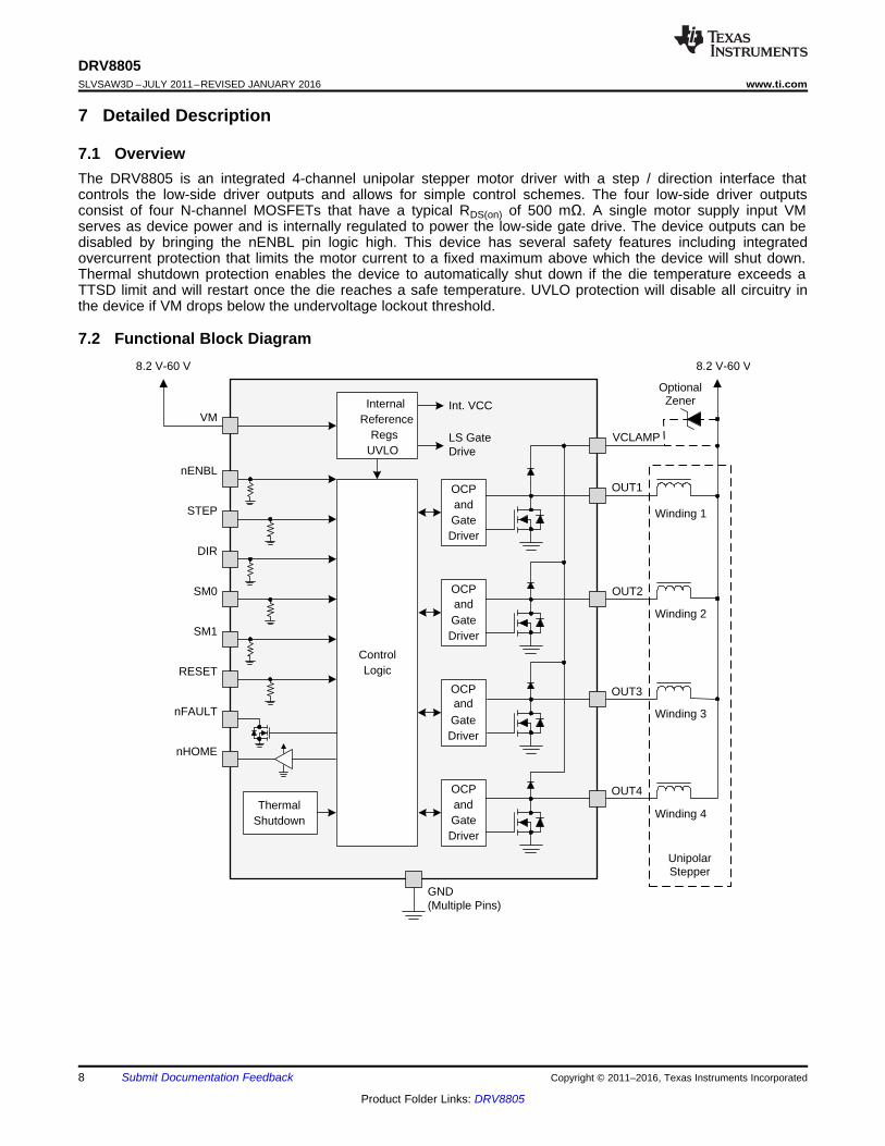
7.1 OverviewThe DRV8805 is an integrated 4-channel unipolar stepper motor driver with a step / direction interface thatcontrols the low-side driver outputs and allows for simple control schemes. The four low-side driver outputsconsist of four N-channel MOSFETs that have a typical RDS(on) of 500 mΩ. A single motor supply input VMserves as device power and is internally regulated to power the low-side gate drive. The device outputs can bedisabled by bringing the nENBL pin logic high. This device has several safety features including integratedovercurrent protection that limits the motor current to a fixed maximum above which the device will shut down.Thermal shutdown protection enables the device to automatically shut down if the die temperature exceeds aTTSD limit and will restart once the die reaches a safe temperature. UVLO protection will disable all circuitry inthe device if VM drops below the undervoltage lockout threshold.
7.2 Functional Block Diagram

OUT1
OUT2
OUT3
OUT4
LookupTable
(Translator)
nENBL
Counter
CLK
RESET
DIR
RESET
STEP
DIR
nHOME
SM0
SM1
9
DRV8805www.ti.com SLVSAW3D –JULY 2011–REVISED JANUARY 2016
Product Folder Links: DRV8805
Submit Documentation FeedbackCopyright © 2011–2016, Texas Instruments Incorporated
7.3 Feature Description
7.3.1 Output DriversThe DRV8805 contains four protected low-side drivers. Each output has an integrated clamp diode connected toa common pin, VCLAMP.
VCLAMP can be connected to the main power supply voltage, VM. It can also be connected to a Zener or TVSdiode to VM, allowing the switch voltage to exceed the main supply voltage VM. This connection can be beneficialwhen driving loads that require very fast current decay, such as unipolar stepper motors.
In all cases, the voltage on the outputs must not be allowed to exceed the maximum output voltage specification.
7.3.2 Indexer OperationThe DRV8805 integrates an indexer to allow motor control with a simple step-and-direction interface. Logically,the indexer is shown in Figure 6.
Figure 6. Indexer Operation
7.3.3 nENBL and RESET OperationThe nENBL pin enables or disables the output drivers. nENBL must be low to enable the outputs. nENBL doesnot affect the operation of the serial interface logic. Note that nENBL has an internal pulldown.
The RESET pin, when driven active high, resets the internal logic. The indexer is reset to the home state. Allinputs are ignored while RESET is active. Note that RESET has an internal pulldown. An internal power-up resetis also provided, so it is not required to drive RESET at power up.
7.3.4 Protection CircuitsThe DRV8805 is fully protected against undervoltage, overcurrent and overtemperature events.
7.3.4.1 Overcurrent Protection (OCP)An analog current limit circuit on each FET limits the current through the FET by removing the gate drive. If thisanalog current limit persists for longer than the tOCP deglitch time (approximately 3.5 µs), the driver will bedisabled and the nFAULT pin will be driven low. The driver will remain disabled for the tRETRY retry time(approximately 1.2 ms), then the fault will be automatically cleared. The fault will be cleared immediately if eitherRESET pin is activated or VM is removed and re-applied.

10
DRV8805SLVSAW3D –JULY 2011–REVISED JANUARY 2016 www.ti.com
Product Folder Links: DRV8805
Submit Documentation Feedback Copyright © 2011–2016, Texas Instruments Incorporated
Feature Description (continued)7.3.4.2 Thermal Shutdown (TSD)If the die temperature exceeds safe limits, all output FETs will be disabled and the nFAULT pin will be driven low.The STEP input will be ignored. Once the die temperature has fallen to a safe level, operation will automaticallyresume.
7.3.4.3 Undervoltage Lockout (UVLO)If at any time the voltage on the VM pin falls below the undervoltage lockout threshold voltage, all circuitry in thedevice will be disabled, and internal logic will be reset. Operation will resume when VM rises above the UVLOthreshold.
7.4 Device Functional Modes
7.4.1 Step ModesThe SM0 and SM1 pins select the stepping mode of the translator as shown in Table 1.
Table 1. Step ModesSM1 SM0 MODE
0 0 2-phase drive (full step)0 1 1-2 phase drive (half step)1 0 1-phase excitation (wave drive)1 1 Reserved
In all modes, during a fault condition, the STEP input will be ignored. See Protection Circuits for moreinformation.
The sequence of the outputs is shown in Table 2, Table 3, and Table 4.
Table 2. 2-Phase Excitation (Full-Step)Function Step RESET DIR STEP nHOME OUT1 OUT2 OUT3 OUT4
Reset 1 1 X X 0 ON OFF OFF ON
CW 2 0 1 ↑ 1 ON ON OFF OFF
CW 3 0 1 ↑ 1 OFF ON ON OFF
CW 4 0 1 ↑ 1 OFF OFF ON ON
CW to home 1 0 1 ↑ 0 ON OFF OFF ON
CCW 4 0 0 ↑ 1 OFF OFF ON ON
CCW 3 0 0 ↑ 1 OFF ON ON OFF
CCW 2 0 0 ↑ 1 ON ON OFF OFF
CCW to home 1 0 0 ↑ 0 ON OFF OFF ON
Hold X 0 X ↑ no chg no chg no chg no chg no chg

11
DRV8805www.ti.com SLVSAW3D –JULY 2011–REVISED JANUARY 2016
Product Folder Links: DRV8805
Submit Documentation FeedbackCopyright © 2011–2016, Texas Instruments Incorporated
Table 3. 1-2-Phase Excitation (Half-Step)Function Step RESET DIR STEP nHOME OUT1 OUT2 OUT3 OUT4
Reset 1 1 X X 0 ON OFF OFF OFF
CW 2 0 1 ↑ 1 ON ON OFF OFF
CW 3 0 1 ↑ 1 OFF ON OFF OFF
CW 4 0 1 ↑ 1 OFF ON ON OFF
CW 5 0 1 ↑ 1 OFF OFF ON OFF
CW 6 0 1 ↑ 1 OFF OFF ON ON
CW 7 0 1 ↑ 1 OFF OFF OFF ON
CW 8 0 1 ↑ 1 ON OFF OFF ON
CW to home 1 0 1 ↑ 0 ON OFF OFF OFF
CCW 8 0 0 ↑ 1 ON OFF OFF ON
CCW 7 0 0 ↑ 1 OFF OFF OFF ON
CCW 6 0 0 ↑ 1 OFF OFF ON ON
CCW 5 0 0 ↑ 1 OFF OFF ON OFF
CCW 4 0 0 ↑ 1 OFF ON ON OFF
CCW 3 0 0 ↑ 1 OFF ON OFF OFF
CCW 2 0 0 ↑ 1 ON ON OFF OFF
CCW to home 1 0 0 ↑ 0 ON OFF OFF OFF
Hold X 0 X ↑ no chg no chg no chg no chg no chg
Table 4. 1-Phase Excitation (Wave Drive)Function Step RESET DIR STEP nHOME OUT1 OUT2 OUT3 OUT4
Reset 1 1 X X 0 ON OFF OFF OFF
CW 2 0 1 ↑ 1 OFF ON OFF OFF
CW 3 0 1 ↑ 1 OFF OFF ON OFF
CW 4 0 1 ↑ 1 OFF OFF OFF ON
CW to home 1 0 1 ↑ 0 ON OFF OFF OFF
CCW 4 0 0 ↑ 1 OFF OFF OFF ON
CCW 3 0 0 ↑ 1 OFF OFF ON OFF
CCW 2 0 0 ↑ 1 OFF ON OFF OFF
CCW to home 1 0 0 ↑ 0 ON OFF OFF OFF
Hold X 0 X ↑ no chg no chg no chg no chg no chg

VM
VCLAMP
OUT1
OUT2
GND
GND
GND
OUT3
OUT4
nENBL RESET
SM1
SM0
GND
GND
GND
DIR
STEP
nHOME
nFAULT1
2
3
4
5
6
7
8
9
10 11
12
13
14
15
16
17
18
19
20
DRV8805
0.1µF 100µF+
M
+
±
+ ±
12
DRV8805SLVSAW3D –JULY 2011–REVISED JANUARY 2016 www.ti.com
Product Folder Links: DRV8805
Submit Documentation Feedback Copyright © 2011–2016, Texas Instruments Incorporated
8 Application and Implementation
NOTEInformation in the following applications sections is not part of the TI componentspecification, and TI does not warrant its accuracy or completeness. TI’s customers areresponsible for determining suitability of components for their purposes. Customers shouldvalidate and test their design implementation to confirm system functionality.
8.1 Application InformationThe DRV8805 can be used to drive one unipolar stepper motor.
8.2 Typical Application
Figure 7. Typical Application Schematic
8.2.1 Design RequirementsTable 5 lists the design parameters for this design example.
Table 5. Design ParametersDESIGN PARAMETER REFERENCE EXAMPLE VALUE
Supply Voltage VM 24 VMotor Winding Resistance RL 7.4 Ω/phase
Motor Full Step Angle θstep 1.8°/stepMotor Rated Current IRATED 0.75 A
PWM frequency fPWM 31.25 kHz
8.2.2 Detailed Design Procedure
8.2.2.1 Motor VoltageThe motor voltage to use will depend on the ratings of the motor selected and the desired torque. A highervoltage shortens the current rise time in the coils of the stepper motor allowing the motor to produce a greateraverage torque. Using a higher voltage also allows the motor to operate at a faster speed than a lower voltage.

13
DRV8805www.ti.com SLVSAW3D –JULY 2011–REVISED JANUARY 2016
Product Folder Links: DRV8805
Submit Documentation FeedbackCopyright © 2011–2016, Texas Instruments Incorporated
8.2.2.2 Drive CurrentThe current path is starts from the supply VM, moves through the inductive winding load, and low-side sinkingNMOS power FET. Power dissipation losses in one sink NMOS power FET are shown in the following equation.
P = I2 × RDS(on) (1)
The DRV8805 has been measured to be capable of 1.5-A Single Channel or 800-mA Four Channels with theDW package and 2-A Single Channel or 1-A Four Channels with the PWP package at 25°C on standard FR-4PCBs. The maximum RMS current will vary based on PCB design and the ambient temperature.
8.2.3 Application Curves
Figure 8. Current Ramp With a 16-Ω, 1-mH,RL Load and VM = 8.2 V
Figure 9. Current Ramp With a 16-Ω,1-mH RL Load and VM = 30 V
Figure 10. OCP With 8.2 V andOUT1 Shorted to VM
Figure 11. OCP Separated by tRETRY With VM = 8.2 V andOUT1 Shorted to VM
+
±
Motor Driver
Power Supply Motor Drive System
VM
GND
+
Local Bulk Capacitor
IC Bypass Capacitor
Parasitic WireInductance
14
DRV8805SLVSAW3D –JULY 2011–REVISED JANUARY 2016 www.ti.com
Product Folder Links: DRV8805
Submit Documentation Feedback Copyright © 2011–2016, Texas Instruments Incorporated
9 Power Supply Recommendations
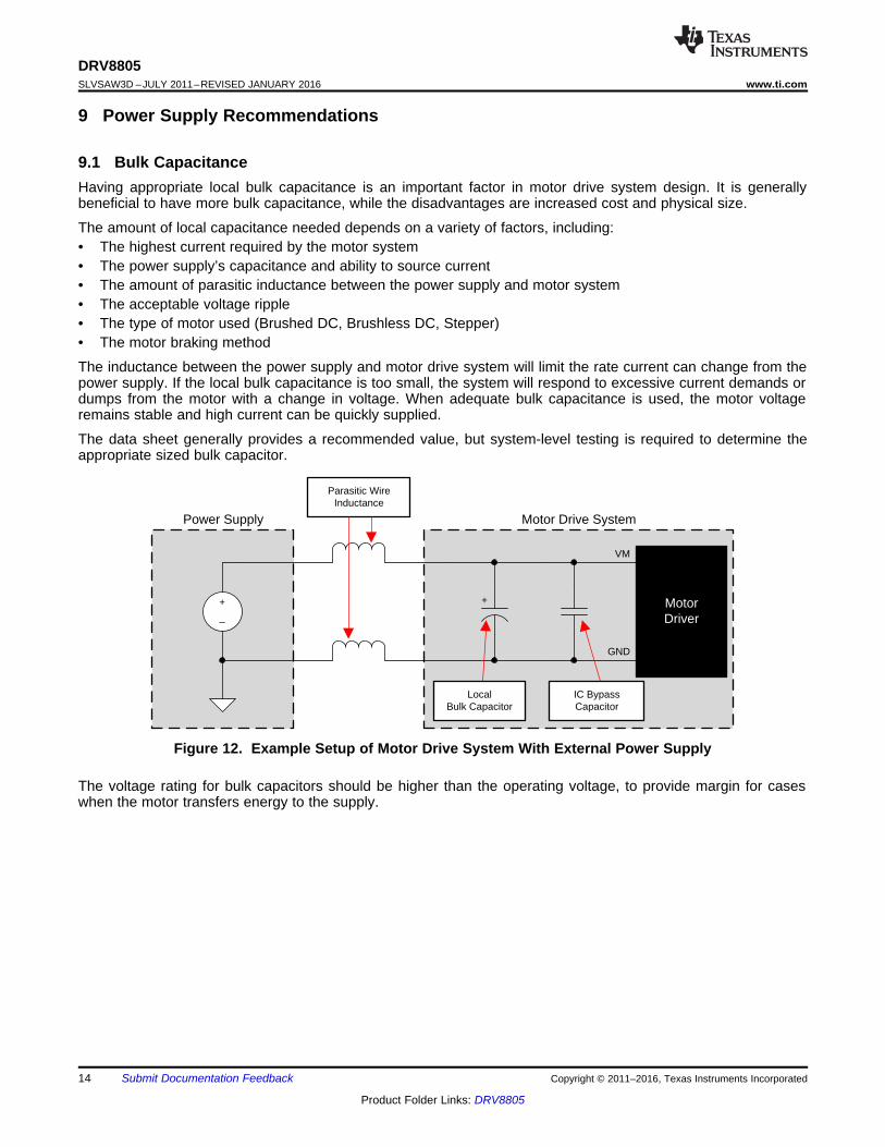
9.1 Bulk CapacitanceHaving appropriate local bulk capacitance is an important factor in motor drive system design. It is generallybeneficial to have more bulk capacitance, while the disadvantages are increased cost and physical size.
The amount of local capacitance needed depends on a variety of factors, including:• The highest current required by the motor system• The power supply’s capacitance and ability to source current• The amount of parasitic inductance between the power supply and motor system• The acceptable voltage ripple• The type of motor used (Brushed DC, Brushless DC, Stepper)• The motor braking method
The inductance between the power supply and motor drive system will limit the rate current can change from thepower supply. If the local bulk capacitance is too small, the system will respond to excessive current demands ordumps from the motor with a change in voltage. When adequate bulk capacitance is used, the motor voltageremains stable and high current can be quickly supplied.
The data sheet generally provides a recommended value, but system-level testing is required to determine theappropriate sized bulk capacitor.
Figure 12. Example Setup of Motor Drive System With External Power Supply
The voltage rating for bulk capacitors should be higher than the operating voltage, to provide margin for caseswhen the motor transfers energy to the supply.

VM
VCLAMP
OUT1
OUT2
GND
OUT3
OUT4
nENBL
nFAULT
nHOME
STEP
DIR
GND
SM0
SM1
RESET
+
15
DRV8805www.ti.com SLVSAW3D –JULY 2011–REVISED JANUARY 2016
Product Folder Links: DRV8805
Submit Documentation FeedbackCopyright © 2011–2016, Texas Instruments Incorporated
10 Layout
10.1 Layout GuidelinesThe bulk capacitor should be placed to minimize the distance of the high-current path through the motor driverdevice. The connecting metal trace widths should be as wide as possible, and numerous vias should be usedwhen connecting PCB layers. These practices minimize inductance and allow the bulk capacitor to deliver highcurrent.• Small-value capacitors should be ceramic, and placed closely to device pins.• The high-current device outputs should use wide metal traces.
The device thermal pad should be soldered to the PCB top-layer ground plane. Multiple vias should be used toconnect to a large bottom-layer ground plane. The use of large metal planes and multiple vias help dissipate theI2 × RDS(on) heat that is generated in the device.
10.2 Layout Example
Figure 13. Example Layout Drawing
10.3 Thermal ConsiderationsThe DRV8805 has thermal shutdown (TSD) as described in Thermal Shutdown (TSD). If the die temperatureexceeds approximately 150°C, the device will be disabled until the temperature drops to a safe level.
Any tendency of the device to enter TSD is an indication of either excessive power dissipation, insufficientheatsinking, or too high an ambient temperature.

P = RDS(ON) · (I )OUT
2
16
DRV8805SLVSAW3D –JULY 2011–REVISED JANUARY 2016 www.ti.com
Product Folder Links: DRV8805
Submit Documentation Feedback Copyright © 2011–2016, Texas Instruments Incorporated
Thermal Considerations (continued)10.3.1 Power DissipationPower dissipation in the DRV8805 is dominated by the power dissipated in the output FET resistance, or RDS(ON).Average power dissipation of each FET when running a static load can be roughly estimated by Equation 2.
where• P is the power dissipation of one FET• RDS(ON) is the resistance of each FET• IOUT is equal to the average current drawn by the load (2)
Note that at start-up and fault conditions this current is much higher than normal running current; these peakcurrents and their duration also must be taken into consideration. When driving more than one loadsimultaneously, the power in all active output stages must be summed.
The maximum amount of power that can be dissipated in the device is dependent on ambient temperature andheatsinking.
Note that RDS(ON) increases with temperature, so as the device heats, the power dissipation increases. This mustbe taken into consideration when sizing the heatsink.
10.3.2 HeatsinkingThe DRV8805DW package uses a standard SOIC outline, but has the center pins internally fused to the die padto more efficiently remove heat from the device. The two center leads on each side of the package should beconnected together to as large a copper area on the PCB as is possible to remove heat from the device. If thecopper area is on the opposite side of the PCB from the device, thermal vias are used to transfer the heatbetween top and bottom layers.
In general, the more copper area that can be provided, the more power can be dissipated.
The DRV8805PWP package uses an HTSSOP package with an exposed PowerPAD™. The PowerPAD™package uses an exposed pad to remove heat from the device. For proper operation, this pad must be thermallyconnected to copper on the PCB to dissipate heat. On a multi-layer PCB with a ground plane, this can beaccomplished by adding a number of vias to connect the thermal pad to the ground plane. On PCBs withoutinternal planes, copper area can be added on either side of the PCB to dissipate heat. If the copper area is onthe opposite side of the PCB from the device, thermal vias are used to transfer the heat between top and bottomlayers.
For details about how to design the PCB, see TI Application Report, PowerPAD™ Thermally Enhanced Package(SLMA002), and TI Application Brief, PowerPAD Made Easy (SLMA004), available at www.ti.com.

17
DRV8805www.ti.com SLVSAW3D –JULY 2011–REVISED JANUARY 2016
Product Folder Links: DRV8805
Submit Documentation FeedbackCopyright © 2011–2016, Texas Instruments Incorporated
11 Device and Documentation Support
11.1 Documentation Support
11.1.1 Related DocumentationFor related documentation see the following:• PowerPAD™ Thermally Enhanced Package, SLMA002.• PowerPAD Made Easy, SLMA004.
11.2 TrademarksPowerPAD is a trademark of Texas Instruments.All other trademarks are the property of their respective owners.
11.3 Electrostatic Discharge CautionThese devices have limited built-in ESD protection. The leads should be shorted together or the device placed in conductive foamduring storage or handling to prevent electrostatic damage to the MOS gates.
11.4 GlossarySLYZ022 — TI Glossary.
This glossary lists and explains terms, acronyms, and definitions.
12 Mechanical, Packaging, and Orderable InformationThe following pages include mechanical, packaging, and orderable information. This information is the mostcurrent data available for the designated devices. This data is subject to change without notice and revision ofthis document. For browser-based versions of this data sheet, refer to the left-hand navigation.

PACKAGE OPTION ADDENDUM
www.ti.com 6-Feb-2020
Addendum-Page 1
PACKAGING INFORMATION
Orderable Device Status(1)
Package Type PackageDrawing
Pins PackageQty
Eco Plan(2)
Lead/Ball Finish(6)
MSL Peak Temp(3)
Op Temp (°C) Device Marking(4/5)
Samples
DRV8805DW ACTIVE SOIC DW 20 25 Green (RoHS& no Sb/Br)
NIPDAU Level-2-260C-1 YEAR -40 to 125 DRV8805DW
DRV8805DWR ACTIVE SOIC DW 20 2000 Green (RoHS& no Sb/Br)
NIPDAU Level-2-260C-1 YEAR -40 to 125 DRV8805DW
DRV8805PWP ACTIVE HTSSOP PWP 16 90 Green (RoHS& no Sb/Br)
NIPDAU Level-3-260C-168 HR -40 to 125 DRV8805
DRV8805PWPR ACTIVE HTSSOP PWP 16 2000 Green (RoHS& no Sb/Br)
NIPDAU Level-3-260C-168 HR -40 to 125 DRV8805
(1) The marketing status values are defined as follows:ACTIVE: Product device recommended for new designs.LIFEBUY: TI has announced that the device will be discontinued, and a lifetime-buy period is in effect.NRND: Not recommended for new designs. Device is in production to support existing customers, but TI does not recommend using this part in a new design.PREVIEW: Device has been announced but is not in production. Samples may or may not be available.OBSOLETE: TI has discontinued the production of the device.
(2) RoHS: TI defines "RoHS" to mean semiconductor products that are compliant with the current EU RoHS requirements for all 10 RoHS substances, including the requirement that RoHS substancedo not exceed 0.1% by weight in homogeneous materials. Where designed to be soldered at high temperatures, "RoHS" products are suitable for use in specified lead-free processes. TI mayreference these types of products as "Pb-Free".RoHS Exempt: TI defines "RoHS Exempt" to mean products that contain lead but are compliant with EU RoHS pursuant to a specific EU RoHS exemption.Green: TI defines "Green" to mean the content of Chlorine (Cl) and Bromine (Br) based flame retardants meet JS709B low halogen requirements of <=1000ppm threshold. Antimony trioxide basedflame retardants must also meet the <=1000ppm threshold requirement.
(3) MSL, Peak Temp. - The Moisture Sensitivity Level rating according to the JEDEC industry standard classifications, and peak solder temperature.
(4) There may be additional marking, which relates to the logo, the lot trace code information, or the environmental category on the device.
(5) Multiple Device Markings will be inside parentheses. Only one Device Marking contained in parentheses and separated by a "~" will appear on a device. If a line is indented then it is a continuationof the previous line and the two combined represent the entire Device Marking for that device.
(6) Lead/Ball Finish - Orderable Devices may have multiple material finish options. Finish options are separated by a vertical ruled line. Lead/Ball Finish values may wrap to two lines if the finishvalue exceeds the maximum column width.
Important Information and Disclaimer:The information provided on this page represents TI's knowledge and belief as of the date that it is provided. TI bases its knowledge and belief on informationprovided by third parties, and makes no representation or warranty as to the accuracy of such information. Efforts are underway to better integrate information from third parties. TI has taken and

PACKAGE OPTION ADDENDUM
www.ti.com 6-Feb-2020
Addendum-Page 2
continues to take reasonable steps to provide representative and accurate information but may not have conducted destructive testing or chemical analysis on incoming materials and chemicals.TI and TI suppliers consider certain information to be proprietary, and thus CAS numbers and other limited information may not be available for release.
In no event shall TI's liability arising out of such information exceed the total purchase price of the TI part(s) at issue in this document sold by TI to Customer on an annual basis.

TAPE AND REEL INFORMATION
*All dimensions are nominal
Device PackageType
PackageDrawing
Pins SPQ ReelDiameter
(mm)
ReelWidth
W1 (mm)
A0(mm)
B0(mm)
K0(mm)
P1(mm)
W(mm)
Pin1Quadrant
DRV8805DWR SOIC DW 20 2000 330.0 24.4 10.8 13.3 2.7 12.0 24.0 Q1
DRV8805PWPR HTSSOP PWP 16 2000 330.0 12.4 6.9 5.6 1.6 8.0 12.0 Q1
PACKAGE MATERIALS INFORMATION
www.ti.com 26-Feb-2019
Pack Materials-Page 1

*All dimensions are nominal
Device Package Type Package Drawing Pins SPQ Length (mm) Width (mm) Height (mm)
DRV8805DWR SOIC DW 20 2000 367.0 367.0 45.0
DRV8805PWPR HTSSOP PWP 16 2000 350.0 350.0 43.0
PACKAGE MATERIALS INFORMATION
www.ti.com 26-Feb-2019
Pack Materials-Page 2


www.ti.com
PACKAGE OUTLINE
C
14X 0.65
2X4.55
16X 0.300.19
TYP6.66.2
0.150.05
0.25GAGE PLANE
-80
1.2 MAX3.552.68
2.461.75
B 4.54.3
A
NOTE 3
5.14.9
0.750.50
(0.15) TYP
PowerPAD TSSOP - 1.2 mm max heightPWP0016JSMALL OUTLINE PACKAGE
4223595/A 03/2017
1
89
16
0.1 C A B
PIN 1 INDEXAREA
SEE DETAIL A
0.1 C
NOTES: 1. All linear dimensions are in millimeters. Any dimensions in parenthesis are for reference only. Dimensioning and tolerancing per ASME Y14.5M. 2. This drawing is subject to change without notice. 3. This dimension does not include mold flash, protrusions, or gate burrs. Mold flash, protrusions, or gate burrs shall not exceed 0.15 mm per side. 4. Reference JEDEC registration MO-153.
SEATINGPLANE
TM
PowerPAD is a trademark of Texas Instruments.
A 20DETAIL ATYPICAL
SCALE 2.500
THERMALPAD
1
8 9
16

www.ti.com
EXAMPLE BOARD LAYOUT
0.05 MAXALL AROUND
0.05 MINALL AROUND
16X (1.5)
16X (0.45)
14X (0.65)
(5.8)
(R0.05) TYP
(3.4)NOTE 8
(5)NOTE 8
(1.35) TYP
(0.65)
(1.3) TYP
( 0.2) TYPVIA
(2.46)
(3.55)
PowerPAD TSSOP - 1.2 mm max heightPWP0016JSMALL OUTLINE PACKAGE
4223595/A 03/2017
NOTES: (continued) 5. Publication IPC-7351 may have alternate designs. 6. Solder mask tolerances between and around signal pads can vary based on board fabrication site. 7. This package is designed to be soldered to a thermal pad on the board. For more information, see Texas Instruments literature numbers SLMA002 (www.ti.com/lit/slma002) and SLMA004 (www.ti.com/lit/slma004). 8. Size of metal pad may vary due to creepage requirement. 9. Vias are optional depending on application, refer to device data sheet. It is recommended that vias under paste be filled, plugged or tented.
TM
SEE DETAILS
LAND PATTERN EXAMPLEEXPOSED METAL SHOWN
SCALE: 10X
SYMM
SYMM
1
8 9
16
METAL COVEREDBY SOLDER MASK
SOLDER MASKDEFINED PAD
15.000
METALSOLDER MASKOPENING
METAL UNDERSOLDER MASK
SOLDER MASKOPENING
EXPOSED METALEXPOSED METAL
SOLDER MASK DETAILS
NON-SOLDER MASKDEFINED
SOLDER MASKDEFINED

www.ti.com
EXAMPLE STENCIL DESIGN
16X (1.5)
16X (0.45)
14X (0.65)
(5.8)
(R0.05) TYP
(3.55)BASED ON
0.125 THICKSTENCIL
(2.46)BASED ON
0.125 THICKSTENCIL
PowerPAD TSSOP - 1.2 mm max heightPWP0016JSMALL OUTLINE PACKAGE
4223595/A 03/2017
2.08 X 3.000.1752.25 X 3.240.15
2.46 X 3.55 (SHOWN)0.1252.75 X 3.970.1
SOLDER STENCILOPENING
STENCILTHICKNESS
NOTES: (continued) 10. Laser cutting apertures with trapezoidal walls and rounded corners may offer better paste release. IPC-7525 may have alternate design recommendations. 11. Board assembly site may have different recommendations for stencil design.
TM
SOLDER PASTE EXAMPLEBASED ON 0.125 mm THICK STENCIL
SCALE: 10X
SYMM
SYMM
1
8 9
16
METAL COVEREDBY SOLDER MASK
SEE TABLE FORDIFFERENT OPENINGSFOR OTHER STENCILTHICKNESSES

www.ti.com
PACKAGE OUTLINE
C
TYP10.639.97
2.65 MAX
18X 1.27
20X 0.510.31
2X11.43
TYP0.330.10
0 - 80.30.1
0.25GAGE PLANE
1.270.40
A
NOTE 3
13.012.6
B 7.67.4
4220724/A 05/2016
SOIC - 2.65 mm max heightDW0020ASOIC
NOTES: 1. All linear dimensions are in millimeters. Dimensions in parenthesis are for reference only. Dimensioning and tolerancing per ASME Y14.5M. 2. This drawing is subject to change without notice. 3. This dimension does not include mold flash, protrusions, or gate burrs. Mold flash, protrusions, or gate burrs shall not exceed 0.15 mm per side. 4. This dimension does not include interlead flash. Interlead flash shall not exceed 0.43 mm per side.5. Reference JEDEC registration MS-013.
120
0.25 C A B
1110
PIN 1 IDAREA
NOTE 4
SEATING PLANE
0.1 C
SEE DETAIL A
DETAIL ATYPICAL
SCALE 1.200

www.ti.com
EXAMPLE BOARD LAYOUT
(9.3)
0.07 MAXALL AROUND
0.07 MINALL AROUND
20X (2)
20X (0.6)
18X (1.27)
(R )TYP
0.05
4220724/A 05/2016
SOIC - 2.65 mm max heightDW0020ASOIC
SYMM
SYMM
LAND PATTERN EXAMPLESCALE:6X
1
10 11
20
NOTES: (continued) 6. Publication IPC-7351 may have alternate designs. 7. Solder mask tolerances between and around signal pads can vary based on board fabrication site.
METALSOLDER MASKOPENING
NON SOLDER MASKDEFINED
SOLDER MASK DETAILS
SOLDER MASKOPENING
METAL UNDERSOLDER MASK
SOLDER MASKDEFINED
www.ti.com
EXAMPLE STENCIL DESIGN
(9.3)
18X (1.27)
20X (0.6)
20X (2)
4220724/A 05/2016
SOIC - 2.65 mm max heightDW0020ASOIC
NOTES: (continued) 8. Laser cutting apertures with trapezoidal walls and rounded corners may offer better paste release. IPC-7525 may have alternate design recommendations. 9. Board assembly site may have different recommendations for stencil design.
SYMM
SYMM
1
10 11
20
SOLDER PASTE EXAMPLEBASED ON 0.125 mm THICK STENCIL
SCALE:6X

IMPORTANT NOTICE AND DISCLAIMER
TI PROVIDES TECHNICAL AND RELIABILITY DATA (INCLUDING DATASHEETS), DESIGN RESOURCES (INCLUDING REFERENCE DESIGNS), APPLICATION OR OTHER DESIGN ADVICE, WEB TOOLS, SAFETY INFORMATION, AND OTHER RESOURCES “AS IS” AND WITH ALL FAULTS, AND DISCLAIMS ALL WARRANTIES, EXPRESS AND IMPLIED, INCLUDING WITHOUT LIMITATION ANY IMPLIED WARRANTIES OF MERCHANTABILITY, FITNESS FOR A PARTICULAR PURPOSE OR NON-INFRINGEMENT OF THIRD PARTY INTELLECTUAL PROPERTY RIGHTS.These resources are intended for skilled developers designing with TI products. You are solely responsible for (1) selecting the appropriate TI products for your application, (2) designing, validating and testing your application, and (3) ensuring your application meets applicable standards, and any other safety, security, or other requirements. These resources are subject to change without notice. TI grants you permission to use these resources only for development of an application that uses the TI products described in the resource. Other reproduction and display of these resources is prohibited. No license is granted to any other TI intellectual property right or to any third party intellectual property right. TI disclaims responsibility for, and you will fully indemnify TI and its representatives against, any claims, damages, costs, losses, and liabilities arising out of your use of these resources.TI’s products are provided subject to TI’s Terms of Sale (www.ti.com/legal/termsofsale.html) or other applicable terms available either on ti.com or provided in conjunction with such TI products. TI’s provision of these resources does not expand or otherwise alter TI’s applicable warranties or warranty disclaimers for TI products.
Mailing Address: Texas Instruments, Post Office Box 655303, Dallas, Texas 75265Copyright © 2020, Texas Instruments Incorporated