Living the Enlightenment in an Age of Revolution: Freemasonry in Bordeaux, 1788-1794
Upload
khangminh22Category
view
3download
0
THÈSE PRÉSENTÉE
POUR OBTENIR LE GRADE DE
DOCTEUR DE
L’UNIVERSITÉ DE BORDEAUX
ÉCOLE DOCTORALE SCIENCES PHYSIQUES ET DE L’INGÉNIEUR
SPÉCIALITÉ ÉLECTRONIQUE
Par Tifenn MARTIN
Air-Filled Substrate Integrated Waveguide (AFSIW)
Filters and Multiplexers for Space Applications
Sous la direction de : Anthony GHIOTTO
(co-directeur : Tan-Phu VUONG)
Soutenue le 17 décembre 2019
Membres du jury :
Mme. MANEUX, Cristell Professeur Université de Bordeaux Présidente
M. BLONDY, Pierre Professeur Université de Limoges Rapporteur
M. BOZZI, Maurizio Professeur Université de Pavie Rapporteur
M. CARPENTIER, Ludovic Docteur CNES Examinateur
M. MARTIN IGLESIAS, Petronilo Ingénieur ESA/ESTEC Examinateur
M. GHIOTTO, Anthony MCF, HDR Bordeaux INP Directeur de thèse
M. VUONG, Tan-Phu Professeur Université de Grenoble Alpes Co-directeur de thèse
M. LOTZ, Frédéric Ingénieur Cobham Co-encadrant
M. DEBORGIES, François Ingénieur ESA/ESTEC Membre invité
M. GOUJON, Christophe Ingénieur DGA Membre invité

i
Synthèse en français
Le Chapitre 1 présente un bref historique de l’avènement des micro-ondes avec une attention particulière sur
leurs implémentations dans les applications spatiales. Le développement des premiers satellites ainsi que les
différentes avancées techniques mises en œuvre pour améliorer les performances des filtres et multiplexeurs sont
expliquées. Le Chapitre 1 donne quelques comparatifs entre les différentes orbites de lancement d’un satellite
ainsi que les tendances économiques actuelles du secteur du spatial qui permettent de mieux comprendre la forte
ascension des constellations de satellites. Ensuite, dans ce même Chapitre, les technologies émergentes de
filtrage sont introduites. Ces technologies sont toutes de bonnes candidates pour leurs implémentations dans les
futures générations de charges utiles de satellites. Un focus particulier est donné à la technologie Air-Filled
Substrate Integrated Waveguide (AFSIW), qui est la technologie avec laquelle les travaux de thèse ont été
développés. Enfin, pour appuyer le choix de la technologie AFSIW, un comparatif des facteurs de qualités
obtenus avec les technologies conventionnelles est donné. Il en ressort que la technologie AFSIW semble être
une excellente candidate en termes de compromis entre la taille, la masse, le coût, et les performances obtenues.
Le Chapitre 2 introduit d’une manière technique la technologie AFSIW. Cette technologie, basée sur les
techniques de circuit imprimé multicouches standard, a pour but d’atteindre les performances électriques de
guides d’ondes métalliques conventionnels tout en gardant un coût de production très faible, car facilement
implémentable en production de masse. La structure du AFSIW y est détaillée ainsi que les différents moyens
d’implémenter les murs électriques. Un comparatif des facteurs de qualités obtenus suivant le choix
d’implémentation des murs électriques est donné. Il s’en suit une démonstration en mesure d’une ligne de
transmission basée sur la technologie AFSIW. Les pertes d’insertion obtenues sont en accord avec les
simulations, ce qui démontre la validité de la structure. Pour étudier la technologie plus en profondeur, des tests
en puissance ont été faits sur le prototype de ligne de transmission. Afin de se rapprocher des conditions
d’utilisations du domaine du spatial, le test de puissance a été mené dans une étuve à vide permettant de
descendre à des pressions de l’ordre de 10-5 mbar. Les tests ont démontré que la structure proposée était capable
de tenir au minimum une puissance de 190 W en CW (Continuous Wave) à une pression de 10-5 mbar. La ligne
de transmission a donc été validée théoriquement, en simulations, en mesures petits signaux, et en mesures de
puissance. De par les bons résultats de cette ligne, un filtre basé sur la technologie AFSIW a été développé. Ce
filtre est un passe-bande du 4ème ordre avec une fréquence de travail de 21 GHz et une bande passante relative
de 1.45%. Le filtre a été conçu en utilisant les méthodes conventionnelles de synthèse de filtre. Puis, il a été
fabriqué et assemblé. Les mesures de ce filtre montrent d’excellents résultats. En effet, toutes les caractéristiques
principales du filtre mesuré sont très proches du filtre simulé. Dans un souci de rigueur et de comparaison, le
filtre a aussi été caractérisé en tests de puissance. Additionnellement au test de puissance sous vide, il a aussi été
choisi d’effectuer un test de multipaction et un test d’effet corona sur le filtre. Ces deux phénomènes sont très
présents dans les applications spatiales et demandent une attention particulière pour les caractériser. Tous les
tests prévus ont été menés à bien et il a été conclu que le filtre développé tenait une puissance de 190 W sous une
pression de 10-5 mbar avec une température stabilisée de 90 °C. De plus, le filtre n’a montré aucun effet
multipactor jusqu’à une puissance de 190 W. Enfin, un effet corona a été déclenché dans le filtre à une pression
critique de 26 mbar avec une puissance d’entrée de 10 W.

ii
Dans le Chapitre 3, une nouvelle topologie de ligne de transmission est développée. Elle a pour but de
souligner le caractère versatile de la technologie AFSIW. Pour cela, les procédés standards des circuits imprimés
sont associés aux procédés de report de composants traversants. Cela ouvre de nouvelles possibilités pour le
développement de la plateforme technologique AFSIW. En effet, la topologie de ligne de transmission
développée permet d’implémenter des composants dits configurables, tels que des déphaseurs, des résonateurs,
et des filtres grâce à un réseau de trous situé dans la couche inférieure et supérieure de la technologie. Dans un
premier temps, la ligne de transmission est étudiée théoriquement. L’implémentation du réseau de trous
augmente les pertes d’insertion de la ligne de transmission. Néanmoins, d’un point de vue masse et thermique,
cette structure est plus performante qu’une ligne de transmission AFSIW conventionnelle. Pour illustrer ce
propos, une ligne de transmission dite PAFSIW (basée sur le principe énoncé précédemment) est fabriquée et
comparée à la ligne de transmission AFSIW développée dans le Chapitre 2. Ces deux lignes sont pesées dans un
premier temps, il est constaté que la ligne perforée permet une réduction de la masse de 22%, ce qui n’est pas
négligeable pour une charge utile. Un test de puissance est ensuite effectué sur les deux structures. Il y est
démontré que l’échauffement de la ligne AFSIW est de 25 °C comparé à l’échauffement de la ligne PAFSIW de
18 °C. La structure permet donc d’améliorer la diffusion thermique grâce au réseau de trous. Il s’en suit le
développement de fonction de base telle que des déphaseurs, des résonateurs, et des filtres. Grâce à l’insertion de
barreaux métalliques traversant de haut en bas la structure, des murs électriques discontinus sont créés, assurant
ainsi la fonction hyperfréquence du composant. Enfin, le principe de diffusion thermique est appliqué sur un
filtre basé sur la structure PAFSIW et est comparé au même filtre basé sur la structure AFSIW. Il est démontré
que le filtre PAFSIW a une meilleure diffusion thermique. Ce principe peut donc être utile dans les applications
à fortes contraintes thermiques.
Le Chapitre 4 détaille l’introduction de zéro de transmission dans des fonctions de filtrage basées sur la
technologie AFSIW. L’aspect multicouche de la technologie est judicieusement utilisé pour implémenter un
chemin secondaire, aussi appelé couplage croisé, pour l’onde électromagnétique. Ainsi, en jouant avec les
déphasages des deux chemins, il est possible de créer une annulation de signal qui causera l’apparition de zéro de
transmission dans les bandes de réjection du filtre. Pour démontrer le principe proposé, un filtre du 3ème ordre
est développé. Les différentes phases des chemins sont étudiées pour trouver la topologie adéquate à
implémenter. Puis, dans un souci de reproductibilité, une analyse de Monte Carlo est menée pour évaluer
l’impact des tolérances de fabrication sur la structure. Une étude sur le possible désalignement des couches et
son impact sur la réponse du filtre est aussi faite. Enfin, comme une partie de l’onde se propage dans un matériau
diélectrique, une étude prenant en compte l’incertitude de la permittivité du matériau est menée pour étudier son
influence sur le comportement du filtre. Il s’en suit une fabrication du prototype et une validation par la mesure.
Le principe ayant été validé sur un filtre d’ordre 3, de manière incrémentale, le principe est adapté à un filtre
d’ordre 4. Les déphasages sont encore une fois étudiés ainsi que les études d’incertitudes. Le prototype est
fabriqué, assemblé, et mesuré. Les résultats sont en excellent accord avec les simulations. Il s’en suit une
remarque critique sur l’implémentation de couplage croisé sur des structures dites “en long”. En effet, le
couplage croisé est implémenté grâce à une ligne de transmission SIW qui possède une longueur électrique
définie. Plus cette longueur est grande, plus la réponse large bande du filtre est susceptible d’être polluée. Pour
contrer cet effet, le principe du couplage croisé est implémenté sur une structure de filtre dite “repliée”. Ce type
de structure permet de rapprocher les résonateurs qui doivent être couplés par le couplage croisé et ainsi réduire

iii
la longueur électrique de la ligne de transmission SIW. Le filtre replié est fabriqué et mesuré. Les résultats sont
en accord avec les simulations. L’amélioration de la réponse large bande du filtre est bien démontrée. Enfin,
dans ce Chapitre, un filtre répondant à des spécifications industrielles est proposé. Ce filtre doit fonctionner en
bande Ku en se conformant à des spécifications sur ses réjections, variations de pertes d’insertion et variations de
temps de groupe. Le filtre proposé pour répondre à cette demande met en application le principe expliqué
ci-dessus. Il est enfin montré par la mesure que le prototype fabriqué respecte bien toutes les spécifications
attendues.
Le Chapitre 5 aborde une problématique souvent négligée par les concepteurs de filtres. Il s’agit de
l’étude du comportement d’un filtre en température. Les filtres embarqués dans des charges utiles de satellites
subissent souvent des changements drastiques de température. Un changement de température du filtre impacte
directement les dimensions physiques du filtre par le biais de dilatations dimensionnelles des matériaux de base
du filtre. Ces changements de dimensions physiques ont pour conséquence de changer la fréquence de résonance
du filtre. Ainsi, si les spécifications de filtrage demandées sont sévères et ne permettent pas de latitude, le filtre
ne remplira plus sa fonction à une température autre que la température ambiante. Pour résoudre ce problème,
l’idée développée dans le Chapitre 5 est de compenser thermiquement le filtre. Ainsi, la fréquence de résonance
du filtre deviendrait indépendante de la température, ce qui assurerait le bon fonctionnement du filtre, peu
importe la température à laquelle il est. Pour cela, la technologie AFSIW est encore une fois utilisée
judicieusement. Le principe proposé pour compenser thermiquement les filtres est de laisser des barreaux de
diélectriques sur le côté des cavités résonantes. En choisissant correctement le diélectrique, il est possible de
trouver un matériau qui a une permittivité qui décroit avec une augmentation de la température et qui augmente
avec une diminution de la température. Pour une augmentation de température donnée, les dimensions de la
cavité se dilateront, causant ainsi la diminution de la fréquence de résonance vers les fréquences basses.
Néanmoins, pour cette même augmentation de température, la permittivité du matériau diminuera, causant
l’augmentation de la fréquence de résonance vers les fréquences hautes. Ainsi, il est possible de trouver les
dimensions adéquates de la cavité et des barreaux de diélectrique pour assurer une stabilisation de la fréquence
de résonance de la cavité avec le changement de température. Les briques de base d’un filtre AFSIW sont des
cavités résonantes et des fenêtres de couplage. Une étude théorique est menée sur l’impact des variations de
température sur les fenêtres de couplage. Il est démontré que cet impact est négligeable. Il est en déduit qu’un
filtre AFSIW peut être compensé thermiquement si et seulement si les cavités de ce filtre sont compensées
thermiquement. La mise en application du principe proposé est démontrée en mesure. Dans un premier temps et
dans un souci de comparaison, un filtre non-compensé et un filtre compensé thermiquement sont fabriqués et
comparés à température ambiante. Le filtre compensé thermiquement présente une augmentation de ses pertes
d’insertion, ce qui est attendu, car des pertes diélectriques sont ajoutées. Puis, une mesure en température est
réalisée. Il est démontré expérimentalement que le filtre compensé thermiquement permet d’avoir une stabilité
thermique de la fréquence de résonance de l’ordre du ppm/°C, ce qui est très semblable à la stabilité thermique
de matériau thermiquement noble, comme l’Invar, qui a cependant un coût très élevé.
Le Chapitre 6 présente la mise en application de tous les principes développés dans les Chapitres
précédents pour la conception d’un multiplexeur d’entrée, plus communément appelé IMUX, d’une charge utile
de satellite. Les spécifications demandées pour cet IMUX portent dans un premier temps sur la réduction de

iv
masse et d’empreinte au sol. La technologie AFSIW développée dans le Chapitre 2 est un très bon candidat pour
répondre à ces contraintes. De plus, l’IMUX présente de fortes contraintes sur ses isolations entre bandes
passantes. Pour répondre à ce critère, le principe développé dans le Chapitre 4 est implémenté sur cet IMUX.
L’IMUX doit également pouvoir être opérationnel sur la gamme de température -20 °C/+70 °C. Ainsi, le
principe développé dans le Chapitre 5 est implémenté afin de s’affranchir de la gamme de température. Enfin,
l’IMUX peut être sensible aux défauts de fabrication. Pour contrer cela, les principes expliqués dans le
Chapitre 3 peuvent être mis en place pour contrer ce phénomène. Différentes configurations d’IMUX sont
données et les avantages et inconvénients de chaque configuration sont regroupés dans un tableau. En se basant
sur les spécifications demandées en termes de taille, poids, et performances, la configuration d’IMUX couplé par
un « manifold » est adoptée. Puis, la configuration géométrique dite « herringbone » est choisie en prenant en
compte les mêmes arguments énoncés précédemment. L’IMUX est ensuite développé avec la technologie
AFSIW en mettant en application les principes développés tout au long de cette thèse. Les simulations du
composant sont données. Cependant, la fabrication n’étant pas encore terminée à l’heure où cette thèse est
rédigée, les résultats expérimentaux de l’IMUX seront présentés durant la soutenance orale de ces travaux.
La thèse est ensuite conclue en récapitulant les éléments majeurs développés. Ces travaux de thèse
représentent une base solide pour les développements futurs de la technologie AFSIW. Une analyse critique est
ensuite donnée sur les travaux qu’il serait judicieux de mener pour étayer les techniques développées.

v
Contents
Synthèse ........................................................................................................................................... i
Contents .......................................................................................................................................... v
Acronyms .................................................................................................................................... viii
Introduction ................................................................................................................................... 1
1. General Context of the Study ................................................................................................... 3
1.1. Milestones in Microwave Engineering with Particular Focus on Space Applications ........ 3
1.2. Satellites Orbits and Constellations ..................................................................................... 7
1.2.1 Geostationary Earth Orbit .......................................................................................... 8
1.2.2 Medium Earth Orbit ................................................................................................... 9
1.2.3 Low Earth Orbit ......................................................................................................... 8
1.3. Launch and Space Conditions ........................................................................................... 10
1.3.1 Vibrations and Shocks ............................................................................................. 10
1.3.2 Temperature and Radiation ...................................................................................... 10
1.3.3 Vacuum and Multipaction ........................................................................................ 11
1.4. Market Trends and Technology Impact ............................................................................. 11
1.5. Satellite, Satellite Constellations and Frequency Bands .................................................... 12
1.5.1 Satellite Constellations ............................................................................................. 12
1.5.2 Satellite Mega-Constellations .................................................................................. 13
1.5.3 Satellite Frequency Bands ........................................................................................ 13
1.5.4 Communication Satellite Architecture ..................................................................... 14
1.6. Emerging Filter Technologies and Techniques ................................................................. 15
1.6.1 Non-Planar Technologies ......................................................................................... 15
1.6.1.1 Multi-Band Techniques .............................................................................. 16
1.6.1.1 Additive Manufacturing Techniques .......................................................... 16
1.6.2 Planar Technologies ................................................................................................. 17
1.6.2.1 Micro-machined Technology ...................................................................... 17
1.6.2.2 Additive Micro-machined Technology ....................................................... 17
1.6.2.3 Substrate Integrated Waveguide Technology ............................................. 18
1.6.2.4 Substrate Integrated Suspended Line Technology ...................................... 18
1.6.2.5 Air-Filled Substrate Integrated Waveguide Technology ............................ 18
1.6.2 Resonator Technologies ........................................................................................... 19
2. AFSIW Technological Platform ............................................................................................. 25
2.1. Air-Filled Substrate Integrated Waveguide Structure ....................................................... 25
2.2. Air-Filled Substrate Integrated Waveguide Transmission Line ........................................ 28
2.2.1 Loss Mechanism ...................................................................................................... 28
2.2.1.1 Conductor Losses ....................................................................................... 29
2.2.1.2 Dielectric Losses ......................................................................................... 29
2.2.1.3 Surface Roughness Effect ........................................................................... 29
2.2.1.4 Radiation Losses ......................................................................................... 30
2.2.2 AFSIW to RWG Transition ..................................................................................... 30
2.2.3 AFSIW Transmission Line ...................................................................................... 32
2.2.4 AFSIW Transmission Line Power-Handling ........................................................... 33
2.3. Air-Filled Substrate Integrated Waveguide Filter ............................................................. 37
2.3.1 Filter Design ............................................................................................................ 38

vi
2.3.2 Experimental Results ............................................................................................... 40
2.3.2 AFSIW Filter Power-Handling ................................................................................ 41
2.3.2.1 Continuous Wave Test ................................................................................ 41
2.3.2.2 Multipactor Test ......................................................................................... 44
2.3.2.2 Corona Test ................................................................................................. 44
3. Configurable Perforated AFSIW Transmission Line .......................................................... 55
3.1. PAFSIW Transmission Line .............................................................................................. 55
3.1.1 PAFSIW Loss Mechanism ....................................................................................... 56
3.1.2 PAFSIW Versus AFSIW ......................................................................................... 57
3.1.2.1 Weight Comparison .................................................................................... 58
3.1.2.2 Transmission Loss Comparison .................................................................. 58
3.1.2.3 Power-Handling and Self-Heating Comparison ......................................... 59
3.2. Configurable PAFSIW Phase Shifters ............................................................................... 61
3.2.1 Theory and Design ................................................................................................... 61
3.2.2 Experimental Results ............................................................................................... 63
3.3. Configurable PAFSIW Resonators .................................................................................... 66
3.4. Configurable PAFSIW Resonator Couplings .................................................................... 68
3.4.1 Monte Carlo Analysis .............................................................................................. 68
3.4.2 Coupling Equivalency .............................................................................................. 70
3.4.3 Through-Hole Mounted Metallic Post Discretized Iris Couplings .......................... 71
3.4.4 Modified Through-Hole Mounted Metallic Post Discretized Iris Couplings .......... 73
3.5. Configurable PAFSIW Filters ........................................................................................... 73
3.5.1 Theory and Design ................................................................................................... 74
3.5.2 Fabrication and Experiment ..................................................................................... 75
3.6. Self-Heating of Filters Based on PAFSIW ........................................................................ 77
3.6.1 Filter Design ............................................................................................................ 77
3.6.2 Experimental Results ............................................................................................... 79
3.6.3 Power-Handling and Self-Heating Comparison....................................................... 81
4. Advanced Filter Responses ..................................................................................................... 85
4.1. Third-Order Cross-Coupled AFSIW Filter ........................................................................ 85
4.1.1 Filter Topology ........................................................................................................ 85
4.1.2 Cross-Coupling Implementation Using AFSIW ...................................................... 88
4.1.3 Filter Design ............................................................................................................ 89
4.1.4 Robustness Against PCB Manufacturing Tolerances .............................................. 90
4.1.5 Experimental Results ............................................................................................... 90
4.2. Quasi-Elliptic Fourth-Order In-Line Configuration AFSIW Filter ................................... 93
4.2.1 Filter Topology ........................................................................................................ 93
4.2.2 Cross-Coupling Implementation Using AFSIW ...................................................... 95
4.2.3 Filter Design ............................................................................................................ 96
4.2.4 Robustness Against PCB Manufacturing Tolerances .............................................. 97
4.2.5 Experimental Results ............................................................................................... 99
4.2.6 Drawbacks of the In-Line Configuration ............................................................... 100
4.3. Quasi-Elliptic Fourth-Order Folded Configuration AFSIW Filter .................................. 101
4.3.1 Filter Topology ...................................................................................................... 101
4.3.2 Cross-Coupling Implementation Using AFSIW .................................................... 101
4.3.3 Filter Design .......................................................................................................... 103
4.3.4 Robustness Against PCB Manufacturing Tolerances ............................................ 103
4.3.5 Experimental Results ............................................................................................. 105
4.4. Higher Order Filter .......................................................................................................... 107
4.4.1 Filter Specifications ............................................................................................... 107

vii
4.4.2 Filter Design .......................................................................................................... 108
4.4.3 Experimental Results ............................................................................................. 110
5. Self-Temperature-Compensated AFSIW Cavities and Filters ......................................... 117
5.1. Background ...................................................................................................................... 117
5.2. Single Slab Self-Temperature-Compensated AFSIW Cavities and Filters ..................... 118
5.2.1 Theory of Single Slab Self-Temperature-Compensated AFSIW Cavities ............. 118
5.2.1.1 Single Slab Air-Filled SIW Cavity Equivalent Multiphysics Transmission Line
Model ....................................................................................................... 118
5.2.1.2 Theoretical Analysis ................................................................................. 121
5.2.1.3 Theoretical and Eigenmode Results Comparison ..................................... 121
5.2.1.4 Metallized Via-Hole Single Slab Self-Temperature compensated AFSIW
Cavity Equivalent Width ......................................................................... 123
5.2.2 Single Slab Self-Temperature-Compensated Quasi-Elliptic AFSIW Filters ......... 124
5.2.2.1 Expansion of Inductive Iris and Coupling Drift ....................................... 124
5.2.2.2 Design of a Single Slab Self-Temperature-Compensated Seventh-Order
AFSIW Filter Demonstrator .................................................................... 126
5.2.2.3 Experimental Results at Ambient Temperature ........................................ 127
5.2.2.4 Experimental Results Versus Temperature Variation .............................. 129
5.3. Double Slab Self-Temperature-Compensated AFSIW Cavities and Filters .................... 131
5.3.1 Theory of Double Slab Self-Temperature-Compensated AFSIW Cavities ........... 131
5.3.1.1 Double Slab Air-Filled SIW Cavity Equivalent Multiphysics Transmission
Line Model ............................................................................................... 132
5.3.1.2 Theoretical Analysis ................................................................................. 133
5.3.1.3 Theoretical and Eigenmode Results Comparison ..................................... 134
5.3.1.4 Post-Process Temperature Compensation Tuning .................................... 135
5.3.2 Double Slab Self-Temperature-Compensated AFSIW Cavities ............................ 136
5.3.2.1 Metallized Via-Hole Double Slab Self-Temperature-Compensated AFSIW
Cavity Equivalent Width ......................................................................... 137
5.3.2.2 Experimental Validation ........................................................................... 137
5.3.2.3 Experimental Post-Process Temperature Compensation Tuning Validation141
5.3.3 Double Slab Self-Temperature-Compensated AFSIW Filters ............................... 142
5.3.3.1 Design of a Self-Temperature-Compensated Fourth-Order AFSIW Filter
Demonstrator ........................................................................................... 142
5.3.3.2 Experimental Results at Ambient Temperature ........................................ 143
5.3.3.3 Experimental Results Versus Temperature Variation .............................. 145
6. Very Compact IMUX for Broadband Applications ........................................................... 149
6.1. Background and Objectives ............................................................................................. 149
6.2. Design Specifications ...................................................................................................... 149
6.3. IMUX Configuration ....................................................................................................... 150
6.4. IMUX Design .................................................................................................................. 152
6.4.1. Channel Filters ...................................................................................................... 152
6.4.2. Manifold Coupled Channel Filters ........................................................................ 156
Conclusions and Future Work ................................................................................................ 161
List of Publications .................................................................................................................... 165
Résumé ....................................................................................................................................... 168
Abstract ...................................................................................................................................... 170

viii
Acronyms
AFSIW Air-Filled Substrate Integrated Waveguide
APHC Average Power Handling Capability
BW Bandwidth
CM Coupling Matrix
CNES Centre National d’Études Spatiales
CTE Coefficient of Thermal Expansion
CW Continuous Wave
DUT Device Under Test
DR Dielectric Resonator
EM Electromagnetic
EMC Electromagnetic Compatibility
EPC Electronic Power Conditioner
ESA European Space Agency
FR-4 Flame Resistant 4
GEO Geostationary Earth Orbit
GNSS Global Navigation Satellite System
GPS Global Positioning System
HPA High-Power Amplifier
HTS High-Temperature Superconductors
IL Insertion Loss
IMUX Input Multiplexer
IoT Internet of Thing
ITU International Telecommunication Union
LEO Low Earth Orbit
LNA Low Noise Amplifier
LO Local Oscillator
LTCC Low Temperature Co-Fired Ceramics
MEO Medium Earth Orbit
MMIC Monolithic Microwave Integrated Circuit
OMUX Output Multiplexer
PAFSIW Perforated Air-Filled Substrate Integrated Waveguide
PCB Printed Circuit Board
PEC Perfect Electric Conductors
PIM Passive InterModulation
RF Radio Frequency
RL Return Loss
RMS Root Mean Square
RWG Rectangular Waveguide
SEY Secondary Electron Yield
SISL Substrate Integrated Suspended Line
SIW Substrate Integrated Waveguide
SL Suspended Line
SLA Stereolithographic
SNR Signal Noise Ratio
SoS System-on-Substrate
SWaP-C Size Weight Power and Cost
tanδ Loss tangent
TCP Thermal Coefficient of Permittivity
TE Transverse Electric
TEM Tranverse Electric Magnetic
Tg Glass Transition Temperature
THM Through-Hole Mounted
TM Transverse Magnetic

ix
TMTC Telemetry and Telecommand
TRL Thru-Reflect-Line
Tz Transmission zero
VNA Vector Network Analyzer
VSAT Very Small Aperture Terminals
WR Waveguide, Rectangular
3D Three-dimensional space
5G Fifth generation of mobile

Introduction 1
Introduction
With the emergence of novel microwave and millimeter-wave applications in the automotive and
communication sectors including the internet of things (IoT), the fifth generation of mobile (5G), and the new
space, innovative technologies providing size, weight, power, and cost (SWaP-C) reduction are highly desired.
In fact, since the last decades, the space market has significantly grown and is expected to provide satellite
services (television, the Internet…) to more people on the Earth’s surface. Hence, the space industry is
undergoing a change of paradigm that pushes it to implement mega-constellation satellite to furnish a global
communication service. To meet the projected high-volume market demands, future microwave and
millimeter-wave components are expected to provide high integrability, lightweight, high power-handling, and
low loss at a reduced cost compared to their counterparts based on conventional technologies. Furthermore,
the stringent specifications of the foreseen systems require rapid synthesis, with high robustness to
manufacturing tolerances, and a low sensitivity to external environment. All those challenges represent a
technological gap for the new generation of satellite payload.
Among the satellite payload components, filters and multiplexers are crucial components in the
architecture. The stringent specifications in terms of low loss, selectivity, out-of-band rejections guide the
microwave community to use the conventional air-filled metallic waveguide technology to meet the desired
electrical performances. Moreover, the conventional air-filled metallic waveguide technology has a low
sensitivity to the space environment and is well mastered by the space industry. Nevertheless, the prohibitive
cost, large size, and high weight characteristics are detrimental for the foreseen applications, in particular for
implementation in the emerging new space applications. Indeed, with the foreseen rise in frequency, the future
generation of filters and multiplexers need to have high performance at an effective cost.
In the presented new space context, the Air-Filled Substrate Integrated Waveguide (AFSIW)
technology combining the advantages of the planar technologies and the conventional air-filled rectangular
waveguide technology is expected to contribute to the development and democratization of the emerging novel
microwave and millimeter-wave low-cost space applications. Furthermore, the AFSIW technology inherits the
high integration characteristics of the Substrate Integrated Waveguide (SIW) and the so-called System on
Substrate (SoS) paradigm can be implemented for the future satellite communication systems. The AFSIW
technological platform has demonstrated to be a successful technological trade-off in terms of size, weight,
power, and cost (SWaP-C) and seems to be a good candidate for the implementation of next future generations
of filters and multiplexers.
Consequently, this Doctoral Thesis investigates the feasibility of Air-Filled Substrate Integrated
Waveguide technology applied to space applications, in particular, to microwave filters and multiplexers.
The Thesis is organized as follows:
Chapter 1 is devoted to a general context of the study. A brief sum up of the milestones in microwave
engineering with particular focus on space applications is described. The space context is then presented with

Introduction 2
the different important aspect to take into account for the implementation of a microwave filter in a satellite
payload. Finally, the emerging filter technologies and techniques are presented.
The second Chapter presents an overview of the AFSIW technological platform. A transmission line
and a bandpass filter operating in the Ka-band satellite communication frequency range are designed and
demonstrated. A mechanical test fixture is also fabricated to be able to characterize those components in small
and high-power signal. The first power-handling tests (continuous wave power-handling test, multipactor test,
and corona test) on AFSIW technology are also reported.
In Chapter 3, an original AFSIW structure based on the conventional PCB and the through-hole
mounting (THM) process, with enhanced robustness to manufacturing tolerances is introduced. It opens up
new possibilities for the AFSIW technological platform as a configurable transmission line is demonstrated.
This configurable component is able to implement different microwave component functions, such as phase
shifters, resonators, and filters. Moreover, an original method to tune resonator frequency is proposed. Finally,
the high interest of this structure is highlighted with an enhanced thermal dissipation compared to conventional
AFSIW.
Chapter 4 is dedicated to the implementation of transmission zeros in the AFSIW technological
platform. Thus, the multilayer aspect of the technology is profitably used to create transmission zeros in AFSIW
filters using an SIW transmission line in the bottom substrate to cross-couple non-adjacent cavities. The
principle is first demonstrated on classical topologies, such as third-order and fourth-order filter. The concept
is extended to a higher order filter face to real filtering specifications, in terms of rejections, insertion loss
variation, and group delay variation. The specifications were proposed by ESA (European Space Agency) and
CNES (Centre National d’Études Spatiales) with the aim of implementing this filter in an Input Multiplexer.
Chapter 5 details the problems linked to temperature drift for microwave filter. Two temperature
compensation techniques for AFSIW filters are introduced. The two techniques are developed such as it can
be adapted to any component based on AFSIW cavities. The principles are developed in the Ku-band, for the
need of ESA and CNES, and extended in the Ka-band for future implementation. It is demonstrated that the
AFSIW technology, based on PCB process, can achieve a comparable thermal stability than costly and high-
performance materials, such as Invar.
Finally, Chapter 6 presents the implementation of all the principles introduced in the previous
Chapters into an IMUX using the AFSIW technology. The IMUX specifications were proposed by ESA and
CNES to address most of the actual IMUX problematic. Unfortunately, the measurements of this IMUX are
not done yet. Thus, only simulations will be shown in this manuscript.
In the Conclusions, the results of this Doctoral thesis are summarized. An overview of the developed
techniques for AFSIW filters are given as well as the foreseen future work.

Chapter 1. General Context of the Study 3
Chapter 1
General Context of the Study
1. 1. Milestones in Microwave Engineering with Particular Focus
on Space Applications
The foundations of microwave theory were established by scientists like Maxwell (1879), Hertz (1894),
Marconi (1937), Lodge (1940), Tesla (1943), and Loomis (1975) over about 100 years ago [1]. The formal and
theoretical foundations of electromagnetic theory was presented by Maxwell in A treatise on Electricity and
Magnetism. Even though many contributors participated in the development of the electromagnetic before
1900, Maxwell’s work stated the existence of electromagnetic waves traveling at the speed of light [2].
Maxwell’s theory and equations, by associating electricity and magnetism, write down the microwave theory
and engineering. The past, present, and future applications based on electromagnetic theory, such as radio,
television, generation of mobile networks, satellite systems, and radio detection and ranging (radar) systems,
are based on the theoretical foundations of Maxwell.
World War II has substantially contributed to technological innovations. It is sometimes referred to
as the Physicist’s War because for the first time, technological innovation was at the heart of the battlefield [3].
In the early 1920s, emerging radar technology providing the potential of detecting planes, ships, and
submarines and to determine their location attracted the attention of military researchers. This is why, in the
1940s, the first major radar installation was constructed along the southern and eastern English coast by the
Royal Air Force to detect the incoming German bombers. This installation was called Chain Home and is one
of the first practical application of microwave theory. The effectiveness of the radar technology led to
unprecedented stimulus to develop microwave theory and technique for civil and military applications [4].
In the 1890s, the development of radio was growing, and many scientists and physicists believed that
radio waves could not travel long distances. This was assumed because the direction of propagation of waves
was in straight lines. In 1901, Marconi proved them wrong with the first message transfer from Great Britain
to Canada over the Atlantic Ocean using a wireless telegraph [5]. Later on, Kennelly and Heaviside proposed
that the long radio waves used by Marconi were bouncing off an atmospheric layer of ions, today called
ionosphere. The British scientist Appleton proved its existence in 1924. The proposed concept of bouncing off
the ionosphere foreshadowed the modern communications satellite.
Satellite communications were some of the first commercial microwave worldwide application. The
world’s first satellite was launched in October 1957, by the Soviet Union, under the name of Sputnik I. The
satellite was launched into an elliptical orbit and was a 58 cm diameter metal sphere and weighted 84 kg.
Following Sputnik I, the Soviet Union launched Sputnik II and thus triggered what is today called the Space
Race. The first United States artificial satellite was launched in January 1958, under the name of Explorer I. It
was the first satellite to detect the Van Allen radiation belt. On August 12, 1960, the United States deployed
Echo I in low orbit earth (LEO), this satellite was designed specifically for microwave communications.

Chapter 1. General Context of the Study 4
Indeed, the metallic surface of Echo I was used to reflecting the incident waves to link two different ground
stations. Hence, Echo I was the first and the last satellite to be described as a passive satellite, as the next
communication satellites implement active components such as mixers and amplifiers.
Satellite communications became more and more popular due to their diverse applications and turned
out to be the first major civilian applications of microwave engineering, after TV. In the late 1960s, the launch
of Intelsat I, II, and III series established the strong basis of satellite applications for voice communications. In
1971, Intelsat IV series was launched and based on a channelized architecture [6], [7]. At that time, the
microwave filters used for channelization used conventional rectangular waveguide structure based on filter
synthesis techniques developed in [8].
In order to maximize bandwidth and signal efficiency for the satellite, filters, input multiplexers
(IMUXs), and output multiplexers (OMUXs) with low insertion loss are essential. Thus, the chosen filter
technology to implement the uplink/downlink was conventional metallic waveguide. Filters and multiplexers
were fabricated using iris-coupled Invar cavities to ensure low insertion loss and a good thermal behavior.
Based on the proposed technology, the developed filters and multiplexers were bulky and heavy, a typical
channel filter had a mass approximating 4 kg [7]. At that time, multiplexers represented nearly 40% of the
payload weight. The mass of these filters became crucial and many methods were introduced to reduce it. The
first technique to reduce the mass of these multiplexers was to reduce the waveguide wall thickness while
meeting the necessary manufacturing constraints [7]. The second technique introduced to minimize the mass
of the filters and multiplexers was to use lightweight materials, such as Kevlar or graphite [9]. This technique
enabled sufficient weight reduction to accommodate 24 channels for the first time in the U.S. domestic satellite
launched in 1975 [10]. Nevertheless, these filters were more complex to fabricate than conventional Invar
filters, and new ideas were needed to develop the future of satellite communications.
The use of two orthogonal degenerate modes in a single cavity was first suggested by Lin [11] in 1951.
Then, a practical implementation of dual-mode filters was established by [12] in 1969. This led to an impetus
for the development of dual-mode filters which settled the theoretical foundations and viability of this topology
[13]-[15]. A classical dual-mode in-line waveguide filter is presented in Fig. 1.1. Taking advantage of
perpendicular modes, dual-mode filters allow a single physical cavity to behave as two electrical ones. In the
classical dual-mode in-line filter, each cavity supports two orthogonal transverse electric (TE) modes TE101
and TE111 [13]. The two modes are coupled with a tuning screw orientated at 45° to the input iris [14]. The
proposed structure also had the advantage to allow coupling between non-adjacent cavities, permitting the
implementation of transmission zeros. Moreover, the principle of dual-mode filters provides a substantial mass
and space savings as the number of physical resonators can be divided by 2, while achieving comparable
electrical function, compared to conventional iris-coupled metallic waveguide filters [15]. The major
development of dual-mode filters were incorporated in Intelsat IV in 1976 [16]. From then on, dual-mode filters
became the satellite industry standard.
Next to the dual-mode filter development, it was intuitive for microwave researchers to focus their
work in implementing more than two modes in a single physical cavity. Triple- and quadruple-mode resonators
have been investigated. In order to have a single cavity that supports three modes, researchers had to find a
mode that could resonate at the same frequency and be orthogonal with the two existing TE101 and TE111 modes.
The challenge was to find an iris structure that can control three inter-cavity simultaneously. In [17], variety of

Chapter 1. General Context of the Study 5
mode charts for rectangular and circular waveguide had been developed. After identifying the potential three
existing modes in a single cavity, a new iris structure capable of providing three independent inter-cavity
couplings must be implemented. This type of iris structure is presented in [18], it also reports the first true
elliptic six-pole triple-mode filter. Later on, quadruple-mode resonators have been studied. This configuration
is based on a cylindrical cavity dual orthogonal transverse magnetic (TM) mode. In [19], an eight-pole bandpass
filter based on quadruple-mode is reported. Nevertheless, the triple- and quadruple-mode filter structure were
too sensitive to manufacturing tolerances and have demonstrated poor thermal stability. This is why, most of
the triple-mode and all the quadruple-mode filter has not been used for satellite applications.
The Intelsat IV established the commercial viability of the C-band (6/4 GHz) satellite systems [7].
This impetus led to the adoption of higher frequencies, in particular, the Ku-band (14/12 GHz) for satellite
communications. This rise in frequencies led to a large reduction in size of microwave components. It also led
the standard designs to be obsolete as with the rise in frequencies comes the ascent in insertion loss. Thus, it
raises the challenge of designing high performance microwave components for Ku-band applications. The
logical way to achieve this goal was to increase the unloaded Q of resonators to counter effect the increase of
insertion loss. The practical realization of this principle was the introduction of filters similar to the dual-mode
filter represented in Fig. 1.1. Those filters were based on TE10n and TE11n modes [20]. The physical realization
of these filters implemented the cavity length equal to n time the half-wavelength [21].
Another major advance in microwave filter technology was the introduction of dielectric resonators.
The work on dielectric resonators started in the 1930s. The use of high permittivity dielectric materials offers
large reduction in size and weight compared to conventional waveguide technology [22]. However, high
performance thermally-stable dielectric material was not available until the 1970s. The most significant
development in the implementation of dielectric resonator in a filter function was made by Fiedziuszko [23] in
1982. The proposed filter is shown in Fig. 1.2, it is similar to the dual-mode filter presented previously except
the resonator are loaded with dielectric material. The concentration of electric fields inside dielectric resonators
allows a significant mass and size reduction of the filter while maintaining the same performance of
conventional dual-mode counterparts. To date, the structure has been implemented on several satellite systems.
As for the work on dielectric resonator, the first work on superconductivity started with Onnes who
investigated the behavior of materials when cooled to nearly absolute zero. Later on, Onnes liquefied helium
for the first time in 1908 [24]. Onnes also discovered the superconductivity phenomena in 1911. Thanks to the
work of Bardeen, Cooper, and Schrieffer, the first theory of superconductivity was developed [24]. In 1986,
the discovery of high-temperature superconductors (HTS) by Bednorz and Müller has stimulated the interest
of the microwave community. The main advantage of HTS is to offer a lightweight, compact, and with
near-infinite unloaded Q which made it a good candidate to compete with conventional technologies developed
at that time [25]. The use of HTS technology allowed the implementation of new input and output multiplexers
working in the C-band with a dramatic size and mass saving compared to conventional technologies, typically
dielectric resonator technology [26]. To have a comprehensive view of the different technology, Table 1.1
compares the mass and volume of a C-band IMUX for Intelsat VIII. It is demonstrated that with the use of this
technology, a potential considerable mass and size saving can be achieved and thus extend the life of the
spacecraft and save money [27]. However, reliability is a crucial criterion for space applications and the HTS
technology has not fully proved its performance with highly reliable cryo-cooler operating in space

Chapter 1. General Context of the Study 6
environment. Moreover, the lack of tuning technique for IMUX application has substantially slowed
implementation of this technology in space applications.
Today, most of the IMUX are designed and fabricated with dielectric resonator technology. This
technology is currently the best trade-off in terms of low insertion loss, thermally stable, high-Q, while
maintaining a low volume and low weight. Some IMUX examples developed by Thales Alenia Space are
shown in Fig. 1.3 and Fig. 1.4.
Figure. 1.1. A dual-mode in-line waveguide filter [20].
Figure. 1.2. A dual-mode in-line dielectric resonator waveguide filter [23].
TABLE 1.1
COMPARISON BETWEEN DIELECTRIC RESONATOR AND HTS TECHNOLOGY FOR A C-BAND IMUX [27]
Parameter Dielectric resonator technology Hybrid DR/HTS technology HTS thin film
technology
Channel filters (kg) 26.2 9 4.2
Cryo-cooler + electronics (kg) / 3 3
Cryogenic package (kg) / 3 2
Total mass (kg) 26.2 15 9.2
Total volume (cm3) 51128 12946 7866
Input OutputM01
M23
M14
M12 M34
M36
M45
M60
Dielectric resonator
Coupling iris

Chapter 1. General Context of the Study 7
Figure. 1.3. A Ka-band IMUX [28].
Figure. 1.4. A Ku-band self-equalized IMUX [28].
1. 2. Satellites Orbits and Constellations
The success of Sputnik I had stimulated the development of satellite communication applications. Today,
almost 5000 satellites are orbiting around the planet out of 8378 satellites that have been launched in total since
1957 [30]. The orbit of a satellite represents the distance from the earth. The orbit of a satellite is chosen
depending on the application, the cost, the lifetime, and the launch. The different orbits are listed below and a
brief description is given in the next paragraphs:
▪ Geostationary Earth Orbit (GEO)
▪ Medium Earth Orbit (MEO)
▪ Low Earth Orbit (LEO)

Chapter 1. General Context of the Study 8
A short list of pros and cons of the different orbits is given in Fig. 1.5.
Figure. 1.5. Comparison between the different satellite orbits [29].
1. 2. 1 Geostationary Earth Orbit
A Geostationary Earth Orbit is a geocentric orbit with an altitude around 35786 km above the Earth surface.
The particularity of this orbit enables the satellite to have an orbital period equal to the Earth’s rotation period.
Thus, a satellite placed in GEO maintain the same position over the Earth’s surface a sidereal day. As a result,
a GEO satellite appears fixed in space and do not need a complex tracking system in the ground, hence reduce
the total cost of the communication system.
Due to the high distance in GEO, the signal of those satellites can broadcast to most of the Earth’s
surface, which makes them ideal candidate for observation, television broadcasting, meteorology (Meteosat)
or internet access. Additionally, to those applications, GEO satellites find military applications and weather
monitoring applications as they provide a constant view of the same surface area. A constellation of 3 GEO
satellites equally placed can cover the entire surface of the Earth except for the Polar Regions.
Nevertheless, the connections with GEO satellites can suffer from high latency because of the long
distance from Earth’s surface which makes them prohibitive for any communication application.
Today, the GEO is by far the most used orbit for satellites with more than 300 satellite launches in
this orbit. Fig. 1.6 represents the occupancy of the GEO.
LEO Signal propagation delay (6 ms) Link budget more favorable
Shorter satellite lifetime Complex ground network
Signal propagation delay (70 ms)
Tracking capability for user terminal
Global coverage with 3 satellites > 15 years lifetime
Signal propagation delay (240 ms) Limited orbital slots
MEO
GEO No tracking capability for user terminal
Exposure to solar storm and interference

Chapter 1. General Context of the Study 9
Figure. 1.6. List of satellites in Geostationary Earth Orbit (courtesy of Boeing).
1. 2. 2 Medium Earth Orbit
A Medium Earth Orbit, often called intermediate circular orbit (ICO), is the region of space around Earth above
LEO and below Geostationary Earth Orbit (GEO). In terms of distance, satellites in the MEO are placed at a
distance between 1400 km and 35786 km above the Earth. MEO satellites are much less used compared to
LEO and GEO.
Compared to a LEO satellite, the surface covered by a satellite placed at MEO is larger due to the
more important distance. Considering the Earth’s rotation movement, it has been demonstrated in the past that
a satellite placed at MEO in a polar orbit can cover the entire surface of the Earth within several days.
This orbit is above all used for global navigation satellite systems like Galileo (Europe), Glonass
(Russia), Beidou (China) or GPS (USA). The MEO is used for navigation purposes as it is a compromise
between LEO, which would require too many satellites to ensure constant visibility, and GEO, which do not
cover the entire globe due to the inclinations of satellites.
Even though the signal delay is higher than the one in LEO, satellites placed at MEO are also used for
Earth observation, military applications, and weather forecasting. However, applications that require a
worldwide signal broadcast are not possible with MEO.
1. 2. 3 Low Earth Orbit
A Low Earth Orbit is an Earth-centered orbit at a distance between 160 and 1400 km above the Earth’s surface.
Satellites placed at LEO orbit in a circular pattern. The orbital period of a satellite at this orbit is 128 minutes

Chapter 1. General Context of the Study 10
or less. To be able to track those satellites, it is necessary to have complex ground equipment as they are in
constant movement.
This orbit allows the signal delay to be very small compared to MEO and HEO orbits as this orbit is
closer to the Earth’s surface. A LEO satellite requires less power to amplify the signal for communication
systems compared to a GEO satellite. Hence, the foreseen applications of this orbit are the voice
communication applications, where the signal delay is a crucial factor. Moreover, the satellites placed at LEO
orbit can observe a particular point several times per day due to the low time to complete one orbit. Thus, this
orbit is of particular interest for observation or military observation applications as with a network of satellites,
it is possible to observe a surface’s point any time of the day. This type of orbit is also used for human
spaceflight, for example, the International Space Station is placed in LEO.
Nevertheless, satellites placed at this orbit only cover a small surface of the Earth, to allow a
worldwide communication, it is necessary to have several LEO satellites. To be able to select an orbit, one
must understand the problematic linked to the launch and the impact of space conditions on the different
components. This is detailed in the next Section.
1. 3. Launch and Space Conditions
Space applications impose additional constraints on filters, multiplexers, and systems. Those constraints are
mainly due to the unique aspects and conditions of satellite communications. Therefore, launch and space
conditions led to more stringent specifications for microwave filters. Additionally, to the electrical behavior,
specifications on temperature, pressure, vibrations, and shocks are required. These requirements drive the
design trade-offs and qualification test protocol of microwave filters and multiplexers.
1. 3. 1 Vibrations and Shocks
A satellite is most of the time launched by a rocket. Vibration is a phenomenon usually induced during the
launch of the satellite due to the combustion of motors and accelerations. The launches of the motors, and the
separation of the different stages generated vibrations and shakes resulting in high mechanical tensions, high
shock and can damage the components of the spacecraft. Therefore, the integration of microwave filters and
multiplexers in the payload of a satellite must be designed taking into account those vibrations. This is why,
vibration and shock tests are always performed on the microwave filter itself and on the overall satellite to
ensure the reliability to space environment.
1. 3. 2 Temperature and Radiation
Space conditions rule satellites to operate in an adverse environment. In fact, depending on the position and
orbit of the satellite, spacecraft can face abrupt temperature changes that can go from –160 °C to 150 °C.
Nevertheless, for the payload components, thanks to the thermal shields, the operating temperature range is
usually -20 °C to 60 °C. The RF devices of the satellite are influenced by the temperature changes and so are
their electrical behavior. Hence, it is necessary for microwave filters and multiplexers to be flexible enough to

Chapter 1. General Context of the Study 11
maintain the required electrical behavior while undergoing the unavoidable expansions due to temperature
changes.
Additional design considerations due to radiation need to be taken into account for microwave filters and
multiplexers. Radiation in space comes from fast-moving particles and X-rays. During solar storms,
high-energy particles can penetrate into the satellite’s metal skin. The energy brought by this particle can be
absorbed by microscopic electrical components of a satellite and have a dramatic impact on the system.
Consequently, the components of a satellite must demonstrate high reliability face to this extreme
environmental stress.
1. 3. 3 Vacuum and Multipaction
In space environment, power generation is costly. In order to maximize the power efficiency of a satellite,
low-loss filters and multiplexers is a key aspect during the design considerations. Nevertheless, to ensure a
correct SNR (Signal Noise Ratio), the power levels of the signal must be sufficient. The absence of pressure
added to important signal power level can create an RF breakdown phenomenon called Multipaction. The
multipactor effect is a phenomenon where an electron resonance cumulated with very high incident energy
creates an RF breakdown.
1. 4. Market Trends and Technology Impact
It is shown in Fig. 1.7 that the 2018 worldwide revenues generated by the space industry are 360 billion U.S.
dollars [31]. The overall growth compared to 2017 is 3%. The global space economy is the union of the
non-satellite space industry (82.5 B$) and the satellite space industry (277.4 B$). The non-satellite space
industry is highly funded by the government budgets. The main application of the non-satellite space industry
is mostly human spaceflight and exploration technologies: robotics and motor technologies, biosensors and
chemical sensors, augmented reality devices and 3D tech, laser and imaging technology.
Figure. 1.7. Global satellite industry revenues (2018) [31].

Chapter 1. General Context of the Study 12
The satellite space industry, representing 77% of the global space economy, is composed of the
satellite manufacturing, launch industry, ground equipment, and telecommunications services. Fig. 1.8
represents the revenues of the fourth division of the satellite space industry. The largest segment is the satellite
services despite a 1.7% decrease. This division is composed of consumer services (satellite television, radio,
broadband), fixed satellite services (transponder agreements, managed network services), mobile satellite
services, and earth observation services. This segment is highly depending on the provided consumer services
as it represents almost 82% of the generated revenues. Another major segment is the ground equipment
representing 45% of the satellite industry funding. Ground equipment is composed of network equipment
(gateways, control stations, Very Small Aperture Terminals (VSATs)) and consumer equipment (satellite
dishes, satellite radio equipment, satellite phones and mobile terminals). This segment revenues increased by
5%, especially thank to the growth in GNSS markets and network equipment. The last two segments represent
the core of the space industrial base. In the present context, those segments undergo a significant development
with a 26% and 34% growth for the satellite manufacturing and launch industry, respectively. This growth
reflects the change of paradigm that the space industry is going through at the moment.
Figure. 1.8. Top-level global satellite industry findings [31].
1. 5. Satellite, Satellite Constellations and Frequency Bands
1. 5. 1 Satellite Constellations
With the emerging technological progress in the 1980s (multiple satellite launch, miniaturization of the
components …) and the changes of the market needs (constant link, robustness in time of response), the space
actors start thinking of implementing satellite constellations in low orbit. A satellite constellation is a system
of satellites that work together to achieve a function. This type of system is usually implemented for
applications that need constant contact with a point on the globe or instant global communication is needed.
The first satellite of the first big caliber constellation was launched in 1986. These constellations are called
Global Positioning System (GPS), and is composed of 24 satellites in MEO. Then, for telecommunication
needs, other constellations have been studied and proposed. Among them, Skybridge (64 satellites) designed

Chapter 1. General Context of the Study 13
by Alcatel Space Industries in 1998, Iridium (66 satellites) designed by Motorola, Télédésic (288 satellites)
designed by Microsoft, GlobalStar (48 satellites) designed by Loral. The concept of LEO satellite constellations
allows the implementation of lower price components, higher compactness, and makes the job easier when it
comes to replacing satellites. Unfortunately, at that time, the economic constraints did not allow the
implementation of those satellite constellations.
1. 5. 2 Satellite Mega-Constellations
The essential part of telecommunication satellite services is composed of GEO satellites. It is worthy to note
that some non-GEO satellite constellation (Iridium, 66 satellites) ensures mobile communications. However,
since 2015, the space market undergoes a change of paradigm as numerous satellite mega-constellation projects
in LEO have risen. This type of constellation requires a more consistent number of satellites, typically hundreds
to thousands, to cover the entire surface of the Earth whereas only 3 GEO satellites are enough. The change of
paradigm to implement LEO satellite mega-constellation is essential to lower the time of latency for the
customer. The principal problematic of the proposed concept is the cost of the launch and satellite itself.
Another advantage of the LEO satellite mega-constellations is the versatility of the launch. Due to the high
number of satellites, it is necessary to have several launches to put in place an entire constellation. Thus, this
principle lowers the financial risk as the different launches can be adapted taking into account the success of
the market. Finally, the satellite mega-constellation market is of high interest for private sectors as it has the
potential to address the entire population on Earth.
1. 5. 3 Satellite Frequency Bands
The radio spectrum for satellite systems is listed in Table 1.2. These allocations are periodically
addressed and revised by the ITU (International Telecommunication Union). Due to their low sensitivity to
signal degradation, L- and S-band are mostly used for navigation applications such as the GPS. The C-band,
largely developed in the 1980s, is used for radar applications, and communications satellites. The X-band is
mostly dedicated to military applications. Finally, most of the satellite communication and the broadband
applications are using Ku- and Ka-band. The different applications are illustrated in Fig. 1.9 [32].
TABLE 1.2
FREQUENCY ALLOCATIONS FOR SPACE APPLICATIONS [32]
Name Frequency range (GHz) Applications
L 1 – 2 GPS, satellite mobile services
S 2 – 4 Weather radar, surface ship radar
C 4 – 8 Satellite communications, satellite TV
X 8 – 12 Military satellites
Ku 12 - 18 Satellite communications
Ka 26 - 40 Satellite communications
Q 40 - 50 /
V 50 - 75 /

Chapter 1. General Context of the Study 14
Figure. 1.9. Satellite frequency bands [32].
1. 5. 4 Communication Satellite Architecture
As previously stated, depending on the application, a satellite uses particular frequency allocations. The goal
of a communication satellite is to relay the signal to different ground segments or satellites over allocated
frequency bands. A communication satellite is in most of the cases composed of two main sections. The first
one is the platform, which groups the different elements ensuring the good functionality of the communication
satellite when placed in orbit. The second one is the payload. This section is composed of elements needed by
the communication satellite to process the data and ensure the good behavior of the satellite. For the particular
application developed in this thesis, only the payload section is detailed as the platform section has no
microwave filter or multiplexer embedded (apart from the TMTC modules) [33].
The payload of a communication satellite is composed of antennas, receivers, and transmitters.
Different payload configurations exist, Fig. 1.10 presents one of them. The different components of the
payload, represented in Fig. 1.10, are used to relay a signal between satellites or ground segments. To do so,
first the satellite receives a signal from the ground thanks to an input antenna. Then, an input filter, is used to
select the desired band. This input filter is required to be as low loss as possible since the power level at this
stage of the communication is at its lowest. It is then amplified with a low-noise amplifier (LNA). To address
the correct transmission band, an oscillator is used to transpose the carrier frequency. Then, this received,
filtered and amplified signal is separated into channels with the use of an IMUX (Input Multiplexer). The
divided channels of the signal are then amplified through high-power amplifiers (HPA). The following step is
to combine the signal, using an OMUX (Output Multiplexer) before the transmission to another ground
segment thanks to the output antenna [33].

Chapter 1. General Context of the Study 15
Figure. 1.10. Simplified diagram block of a satellite payload [33].
As it can be observed from Fig. 1.10, microwave and millimeter-wave filters, IMUXs, and OMUXs,
play an important role in a satellite payload. The size and mass of those components are critical for the cost of
the payload. Moreover, the commercial space industry is growing fast, and the past preserved satellite
application market has now opened its doors to new actors. The development of satellites in terms of number,
and size have saturated the present frequency allocations. Moreover, the future generation of mobile and high
data speed internet is in crucial need for bandwidth, which is not suitable with the actual frequency allocations.
Hence, the space actors are pushed towards the use of higher frequency bands, such as Q- and V-band. This
frequency jump will allow the miniaturization of the microwave components, but it will also raise technological
challenges. This is why, today, the space industry is investigating new technologies offering an optimal
trade-off between size, weight, power, and cost (SWaP-C) for future implementation in space applications.
1. 6. Emerging Filter Technologies and Techniques
In this section, several technologies to implement microwave and millimeter-wave filters and multiplexers are
presented. In the presented context, two major families of filter technologies are introduced, the non-planar
family and the planar family. The selection of a technology depends on the foreseen application, taking into
account different specifications, such as mass, volume, cost, electrical performance, and behavior to external
environment. The recent advances in technologies and techniques are presented in the next section. It is
obviously a hard work to sum up all the recent advances, it is tried to give an overview of the different paths
for the future generation of microwave and millimeter-wave filters and multiplexers.
1. 6. 1 Non-Planar Technologies
The non-planar technologies are based on propagation inside a volume of air enclosed by a metallic cover.
Depending on the geometry of the volume, basic and complex filter function can be achieved. In most of the
case, the type of filter is based on a section of hollowed metallic waveguide (rectangular or circular), or
dielectric resonator.
Input
filter LNA
Frequency
converter
Receive
antenna
LO
IMUX Preamp HPA
EPC
OMUX
Transmit
antenna
Receiver HPA subsystem

Chapter 1. General Context of the Study 16
1. 6. 1. 1 Multi-Band Techniques
Most of the communication systems are designed to support different frequency bands. To separate these bands,
a common technique is to use several filters. The use of multi-band filters can lead to a size, mass, and cost
reduction in this context. A single multi-band filter can replace several single-band filter while maintaining the
electrical performances. In satellite communication systems, the use of multi-band filter can substantially
simplify the system architecture. Moreover, the concept of multi-band filter can be extended to multi-band
diplexer, triplexer, and more generally to multiplexer. Different approaches were developed since the 1970s to
implement multi-band in a single filter. The first one consists of using a wideband bandpass filter in which
transmission zeros are implemented in the in-band of the filter [34]-[35]. A second one is based on the use of
multimode resonators, in this case, each band of the multi-band filter corresponds to a propagation mode
[36]-[37]. Another approach relies on using parallel connected filters [38]. Finally, it is also possible to
implement a wideband bandpass filter in which notch reject filters are cascaded [39].
1. 6. 1. 2 Additive Manufacturing Techniques
The additive manufacturing technology, also called 3D printing, is a technique developed since the 1980s. The
principle of the additive manufacturing is to fabricate mechanical elements in a single block which does not
require any interconnection compared to conventional manufacturing process. During the last decades,
substantial improvement has been made with the precision and the metallization techniques for 3D printing
[40]. Thus the additive manufacturing technology allows a cost reduction, fast prototyping, and similar Q-factor
to the conventional air-filled metallic waveguide technology [41]. In the current research, several additive
manufacturing technologies exist [42]. One of the common technique is to directly print the desired component
in metal with the use of laser melting technology [43]. Nevertheless, this technique is very costly and often
offer a poor surface roughness. Another technique is to use the stereolithographic (SLA). This technique is
much cheaper compared to laser melting technology, and allows the components to be lightweight and high
resolution [44]. However, the drawback of this technique is the fragility of the components and also it needs
an additional metallization process. The additive manufacturing is mainly used for non-planar components,
yet, it is possible to use it to implement particular shaped planar components as demonstrated in [45].
The main advantage of the non-planar technologies is to present an extremely high Q-factor (> 1000)
and very low insertion loss (< 1 dB). It also offers a high-power handling compared to other technologies
thanks to the large dimensions. Moreover, as the propagation modes need to be enclosed by a metallic cover,
the non-planar technologies are intrinsically self-shielded. Finally, this type of technology presents an
acceptable thermal stability.
All the different aspects of the non-planar technologies justify their major implementation in most of
the payload configurations. Indeed, those technologies are not only used for the emission part but also for the
reception part. Nevertheless, this type of component exhibits a large footprint, is heavy, and expensive in the
present market. Additionally, the fabricated filters and multiplexers based on the non-planar technologies are

Chapter 1. General Context of the Study 17
complex to manufacture and require a tuning phase, which represents an increased cost in terms of money and
time.
1. 6. 2 Planar Technologies
For applications requiring medium electrical performances, the planar technology is a good candidate to be
implemented. The filters based on planar technologies offer a good compactness, footprint, and mass compared
to non-planar technologies. Moreover, as most of the planar technologies are based on Printed Circuit Board
(PCB) process, this type of technology can hit a high volume of production and address a mass production
market. Thus, their implementation in the future satellite constellation market is of high interest. Finally, their
implementation with other active or passive components, particularly active MMICs is easier and can introduce
new concepts such as the so-called System on Substrate (SoS) [46].
1. 6. 2. 1 Micro-machined Technology
The micro-machined technology is based on the same principle as the microstrip and coplanar technology. The
transmission line sections are implemented on a dielectric membrane of several micrometers. The dielectric
layer is previously deposited on a thicker substrate. Then, the substrate is machined to be replaced by air [47].
Hence, an air-filled cavity is implemented under the coplanar transmission line. In some cases, a metal cavity
is added above the transmission line to create an entirely shielded structure. By removing the dielectric, the
transmission line has a pure TEM propagation mode [48]. This technology allows to reduce substantially the
insertion loss and becomes of high interest for filter implementation. In fact, by removing the dielectric, the
achievable Q-factor considerably increases. The literature reports several filter topologies taking advantage of
micro-machined technology [49]-[53]. However, the high complexity of the fabrication process has slowed
down the commercial acceptance, and complex filter geometry are not easily implementable. Moreover, the
RF ports of the filter must be placed on the edge of the membrane and might lead to undesirous mode in the
substrate and are hard to be integrated with planar components.
1. 6. 2. 2 Additive Micro-machined Technology
The additive micro-machined technology allows depositing multiple metal layers. In most of the case, this
process uses a metal sacrificial layer removal. First, coplanar lines are defined to realize the filter function.
Then, the support of the shielding structure is ensured by the deposit of a polymer. A metal layer is then
deposited on the volume of the polymer. Finally, the polymer is removed to achieve a metallic shield on the
top of the coplanar lines [54]-[56]. Extensive work has been done with the additive micro-machined
technology. High Q-factor was achieved [57]-[58]. This technology benefits from the expertise of the industry
world as microelectronic process has been used for companies for decades and are well mastered. Thus,
additive micro-machined technology allows fabricating very small, high-performance components, and also
“tuning free” filters. However, even if this technology enables to implement complex 3D structure, it requires
a large number of layers to fabricate the entire component, and it is time costly. It should also be noted that it

Chapter 1. General Context of the Study 18
becomes complex to fabricate components with high thickness with this technique and thus limiting the
power-handling capability. Finally, even if this technology can address the mass production market and can be
integrated with MMIC or standard SoS, its cost might be prohibitive for the implementation of the new space
mega-constellation satellite.
1. 6. 2. 3 Substrate Integrated Waveguide Technology
The Substrate Integrated Waveguide (SIW) technology basis is to implement a waveguide structure in a
substrate (planar structure) [59]. The major aspect of the SIW technology is to combine the advantages of the
non-planar metallic waveguide technology with the advantages of planar technologies [60]. The sidewall of
this planar waveguide is ensured by two rows of metallic cylinders or slots. The proposed concept is to achieve
an integrated waveguide-like planar form using existing planar fabrication process techniques. The SIW
technology exhibits similar propagation characteristics to the ones of non-planar rectangular metallic
waveguide. This technology can be used with conventional fabrication process such as PCB or low-temperature
covered ceramic (LTCC). Hence, the proposed SIW technology is well suited for mass production market, easy
to integrate, and is cost-effective [61]. Moreover, this technology allows to introduce the concept of SiP
(System in Package) which can be extended to the SoS concept [62]. SoS is of high interest to fabricate a
cost-effective, easy manufacturing, and high-performance microwave and millimeter-wave platform.
Nevertheless, when it comes to high frequency (> 20 GHz), the dielectric loss introduced by the substrate may
become prohibitive for high performance specifications. In addition, the SIW technology is quite sensitive to
external environment, such as temperature variation.
1. 6. 2. 4 Substrate Integrated Suspended Line Technology
The Substrate Integrated Suspended Line (SISL) technology is based on the Suspended Line (SL) technology.
The SL technology requires a high fabrication cost, as it is based on a mechanical assembly. In the presented
context, the SL technology is bulky, has heavy weight and present low integration possibilities. To overcome
the drawbacks of SL technology, SISL was introduced [63]. SISL is a new technological platform introduced
in 2014. It is based on standard multilayer PCB process to get rid of the additional metal cavity of SL
technology. Thus, it offers compact size, lightweight, low fabrication cost, and self-packaging. It was
introduced to counter effect the weakness of the SL technology.
1. 6. 2. 5 Air-Filled Substrate Integrated Waveguide Technology
The Air-Filled Substrate Integrated Waveguide (AFSIW) technology was introduced in 2014 [64]. It is based
on a multilayer PCB process. In the most conventional form of AFSIW, a bottom and top substrate (substrate
1 and 3) are used to enclose an inner substrate (substrate 2) in which an air region has been manufactured.
Hence, substrate 1 and 3 acts as electric broad-walls and substrate 2 is the propagation medium for the
electromagnetic wave. The electric sidewalls of the AFSIW can be realized with two methods. The first one is
to direct copper-platted the sidewalls, creating a direct waveguide-like structure. The second is to implement
arrays of metallized via to ensure the electromagnetic boundaries. To fabricate those copper cylinders,

Chapter 1. General Context of the Study 19
dielectric slabs on the sidewalls of the waveguide have to be kept [65]. By removing the dielectric in substrate
2, this structure allows to dramatically reduce the insertion loss as the dielectric loss are considered null. If the
dielectric slabs are of small size (depending on the application frequency), the AFSIW technology supports
TE10 fundamental mode [65]. Several components such as filters [66], [67] or antennas [68], [69] have already
been introduced in the literature taking advantage of the technology. This work aims to extend the previous
research.
1. 6. 3 Resonator Technologies
Microwave resonators represent an essential building block for the implementation of bandpass filters. The
geometry of the resonator determines the field distribution of the electromagnetic wave. The major aspects of
a microwave resonator are the size, unloaded Q-factor, power-handling capability, and cost. The unloaded
Q-factor represents the intrinsic losses, depending on the technologies, materials, dimensions, of the resonator.
The higher the Q-factor is, the smaller the losses are.
It can be observed from Fig. 1.11 that the AFSIW technology is in the middle between SIW and
conventional air-filled metallic waveguide. The Q-factor range of AFSIW technology is considered to be from
800 to 3000. It is worthy to say that, higher Q-factor can be achieved, for example by stacking several layers
of air to increase the total height of the resonator. However, it can be noticed that the AFSIW performance is
closed to the non-planar technologies. The cost of the AFSIW remains low as it is based on standard multilayer
PCB process. The size is directly established by the work frequency as the propagation is similar to
conventional metallic waveguide. Nevertheless, Fig. 1.11 does not mention the ability of a technology to stack
components. It is of particular interest, especially for space applications, to be able to stack components as the
critical criteria is often the footprint. In this context, the planar structures, such as AFSIW, are more suitable
to implement stacked components compared to non-planar structures due to their fabrication process.
Figure. 1.11. Comparison of AFSIW resonator technology to conventional technologies.
Q = 50 ~200
Q = 150 ~ 1000
Q = 800 ~ 3000
Q = 200 ~ 3000
Q = 1000 ~ 10000
Size
Loss
Cost
Chapter 1. General Context of the Study 20
1. 7. Conclusions
In this Chapter, a general context of the microwave applications has been discussed. A particular focus on
space applications has been given. The context of new space has been explained and the need for future
generations of satellites to benefit from an alternative technology is well highlighted with the economic context.
Basic knowledge on space applications is explained, such as the different used orbits, satellite launch
conditions, phenomena that a microwave filter can undergo in space. Different emerging technologies are
presented. The high interest of the planar technologies is explained in terms of high integration degree. A
particular attention has been given to the AFSIW technology as this thesis is going to use it. A comparison of
the unloaded Q-factor, cost, and size of microwave resonators based on different technologies is given to allow
the readers to understand the interest of the technology for the development of microwave and millimeter-wave
filtering functions.

Chapter 1. General Context of the Study 21
References
[1] D. M. Pozar, Microwave Engineering, 4th ed. John Wiley, 2012, ch. 6, pp. 272-316.
[2] Maxwell, J. (2010). A treatise on electricity and magnetism (Cambridge Library
Collection - Physical Sciences). Cambridge: Cambridge University Press.
[3] F. E. Terman, “A brief history of electrical engineering education,” Proceedings of the IEEE, vol.
86, no. 8, pp. 1792-1800, Aug. 1998.
[4] A. A. Oliner, “Historical perspectives on microwave field theory,” IEEE Transactions on
Microwave Theory and Techniques, vol. 32, no. 9, pp. 1022-1045, Sep. 1984.
[5] H. Sobol, and K. Tomiyasu, “Milestones of microwaves,” IEEE Transactions on Microwave Theory
and Techniques, vol. 50, no. 3, pp. 594-611, Mar. 2002.
[6] E. T. Jilg et al., ‘The Intelsat IV spacecraft,” Comsat Technical Review, vol. 2, no. 2, Fall 1972.
[7] C. Kudsia, R. Cameron, and W.-C. Tang, “Innovations in microwave filters and multiplexing
networks for communications satellite systems,” IEEE Digest on Microwave Theory and
Techniques, vol. 40, pp. 1133-1149, Jun. 1992.
[8] S. B. Cohn, “Direct-coupled resonator filters,” Proc. IRE, vol. 45, pp. 187-1976, Feb. 1957.
[9] C. M. Kudsia, and M. V. O'Donovan, “A light weight graphite fiber epoxy composite (GFEC)
waveguide multiplexer for satellite application,” European Microwave Conference, Montreux,
Switzerland, 1974, pp. 585-589.
[10] J. E. Keigler, “RCA Satcom: An example of weight-optimized, satellite design for maximum
communications capacity,” Acta Astronautics. New York: Pergamon, 1978, vol. 5.
[11] W. G. Lin, “Microwave filters employing a single cavity excited in more than one mode,” J. Appl.
Phys., vol. 22, pp. 989–1001, Aug. 1951.
[12] B. L. Blacier and A. R. Champeau, “Dual-mode circular and/or square waveguide filters,” U.S.
Patent 3 697 898, issued Oct. 1972.
[13] A. E. Atia, and A. E. Williams, “New types of waveguides bandpass filters for satellite
transponders,” Comsat Technical Review, vol. 1, no. 1, pp. 21-43, Fall 1971.
[14] A. E. Atia, and A. E. Williams, “Narrow-bandpass waveguide filters,” IEEE Transactions on
Microwave Theory and Techniques., vol. 20, pp. 258-265, Apr. 1972.
[15] A. E. Atia, A. E. Williams, and R. W. Newcom, “Synthesis of dual-mode filters,” IEEE Transactions
on Circuits and Systems, vol. CAS-21, pp. 649–655, Sept. 1974.
[16] J. L. Dicks, and M. P. Brown Jr., “Intelsat IV-A satellite transmission design,” Proc. AIAA 5th
Communications Satellite Systems Conf., Los Angeles, CA, Apr. 1974.
[17] G. L. Matthaie, L. Young, and E. M. T. Jones, “Microwave filters, impedance matching networks,
and coupling structures,” Book Mart press, North Bergen, NJ, USA, Nov. 1985.
[18] W. C. Tang, and S. K. Chaudhuri, “A true elliptic-function filter using triple-mode degenerate
cavities,” IEEE MTT-S Inr. Microwave Symp. Dig., Boston, MA, May 31-June 3, 1983.
[19] R. R. Bonetti, and A. E. Williams, “Application of dual TM-modes to triple and quadruple mode
filters,” IEEE Trans. Microwave Theory Tech., vol. MTT-35, pp. 1143-1149, Dec. 1987.
[20] I. C. Hunter, L. Billonet, B. Jarry, and P. Guillon, “Microwave filters-applications and technology,”
IEEE Transactions on Microwave Theory and Techniques, vol. 50, no. 3, pp. 794-805, Mar. 2002.
[21] S. Kallianteris, and M. V. O’Donovan, “Technology advances in the realization of filter networks
for communications satellites operating at frequencies above IO GHz,” Proc. AIAAKASI 6th
Communications Satellite Systems Conf., Montreal, Apr. 5-8, 1981.
[22] R. D. Richtmyer, “Dielectric resonators,” Journal of Applied Physics, vol. 10, pp. 391-398, Jun.
1939.
[23] S. J. Fiedziuszko, “Dual-mode dielectric resonator loaded cavity filters,” IEEE Transactions on
Microwave Theory and Techniques, vol. MTT-30, pp. 1311–1316, Sept. 1982.
[24] M. J. Lancaster, Passive Microwave Device Applications of High Temperature Superconductors.
Cambridge, MA: Cambridge Univ. Press, 1997.
[25] R. R. Mansour, “Microwave superconductivity,” IEEE Transactions on Microwave Theory and
Techniques, vol. 50, no. 3, pp. 750-759, Mar. 2002.
[26] R. R. Mansour et al., “Design considerations of superconductive input multiplexers for satellite
applications,” IEEE Transactions on Microwave Theory and Techniques, vol. 44, no. 7, pp. 1213-
1228, Jul. 1996.

Chapter 1. General Context of the Study 22
[27] R. R. Mansour et al., “A 60-channel superconductive input multiplexer integrated with pulse-tube
cryocoolers,” IEEE Transactions on Microwave Theory and Techniques, vol. 48, no. 7, pp. 1171-
1180, Jul. 2000.
[28] https://www.thalesgroup.com/sites/default/files/database/d7/asset/document/Imux_Omux.pdf
[29] Constellations Telecom, Euroconsult, 2019
[30] UNOOSA, United Nations Official Document System, 2019.
[31] SIA, State of the Satellite Industry, 2019
[32] https://www.esa.int/spaceinimages/Images/2013/11/Satellite_frequency_bands
[33] T. M. Braun, Satellite Communications Payload and System, 1st ed. John Wiley, 2012.
[34] G. Macchiarella, and S. Tamiazzo, “Design techniques for dual-passband filters,” IEEE
Transactions on Microwave Theory and Techniques, vol. 53, no. 11, pp. 3265-3271, Nov. 2005.
[35] P. Lenoir, S. Bila, F. Seyfert, D. Baillargeat, and S. Verdeyme, “Synthesis and design of
asymmetrical dual-band bandpass filters based on equivalent network simplification,” IEEE
Transactions on Microwave Theory and Techniques, vol. 54, no. 7, pp. 3090-3097, July 2006.
[36] L. Zhu, R. R. Mansour, and M. Yu, “Compact Waveguide Dual-Band Filters and Diplexers,” IEEE
Transactions on Microwave Theory and Techniques, vol. 65, no. 5, pp. 1525-1533, May 2017.
[37] L. Zhu, R. R. Mansour, and M. Yu, “Triple-Band Cavity Bandpass Filters,” IEEE Transactions on
Microwave Theory and Techniques, vol. 66, no. 9, pp. 4057-4069, Sept. 2018.
[38] G. Macchiarella, and S. Tamiazzo, “Dual-Band Filters for Base Station Multi-Band
Combiners,” IEEE/MTT-S International Microwave Symposium, Honolulu, HI, 2007, pp. 1289-
1292.
[39] R. R. Mansour, and P. D. Laforge, “Multiband superconducting filters,” IEEE MTT-S International
Microwave Symposium (IMS), San Francisco, CA, 2016, pp. 1-4.
[40] E. A. Rojas-Nastrucci, J. T. Nussbaum, N. B. Crane, and T. M. Weller, “Ka-band characterization
of binder jetting for 3-D printing of metallic rectangular waveguide circuits and antennas,” IEEE
Transactions on Microwave Theory and Techniques, vol. 65, no. 9, pp. 3099-3108, Sept. 2017.
[41] C. Tomassoni, G. Venanzoni, M. Dionigi, and R. Sorrentino, “Compact quasi-elliptic filters with
mushroom-shaped resonators manufactured with 3-D printer,” IEEE Transactions on Microwave
Theory and Techniques, vol. 66, no. 8, pp. 3579-3588, Aug. 2018.
[42] F. Calignano, D. Manfredi, E. P. Ambrosio, S. Biamino, M. Lombardi, E. Atzeni, A. Salmi, P.
Minetola, L. Iuliano, and P. Fino, “Overview on additive manufacturing technologies,” Proceedings
of the IEEE, vol. 105, no. 4, pp. 593-612, Apr. 2017.
[43] O. A. Peverini, G. Addamo, M. Lumia, G. Virone, F. Calignano, M. Lorusso, and D. Manfredi,
“Additive manufacturing of Ku/K-band waveguide filters: a comparative analysis among selective-
laser melting and stereo-lithography,” IET Microwaves, Antennas & Propagation, vol. 11, no. 14,
pp. 1936-1942, 19 11 2017.
[44] M. Dionigi, C. Tomassoni, G. Venanzoni, and R. Sorrentino, “Simple high-performance metal-
plating procedure for stereolithographically 3-D-printed waveguide components,” IEEE Microwave
and Wireless Components Letters, vol. 27, no. 11, pp. 953–955, Nov. 2017.
[45] E. Massoni, L. Silvestri, G. Alaimo, S. Marconi, M. Bozzi, L. Perregrini, and F. Auricchio, “3-D
printed substrate integrated slab waveguide for single-mode bandwidth enhancement,” IEEE
Microwave and Wireless Components Letters, vol. 27, no. 6, pp. 536-538, Jun. 2017.
[46] Z. Li and K. Wu, “24-GHz frequency-modulation continuous-wave radar front-end system-on-
substrate," IEEE Transactions on Microwave Theory and Techniques, vol. 56, no. 2, pp. 278-285,
Feb. 2008.
[47] Chen-Yu Chi, and G. M. Rebeiz, “Planar millimeter-wave microstrip lumped elements using micro-
machining techniques,” IEEE MTT-S International Microwave Symposium Digest, San Diego, CA,
USA, 1994, pp. 657-660 vol.2.
[48] N. I. Dib, and L. P. B. Katehi, “Impedance calculation for the microshield line,” IEEE Microwave
and Guided Wave Letters, vol. 2, no. 10, pp. 406-408, Oct. 1992.
[49] S. V. Robertson, L. P. B. Katehi, and G. M. Rebeiz, “Micromachined self-packaged W-band
bandpass filters,” IEEE MTT-S International Microwave Symposium, Orlando, FL, USA, 1995, pp.
1543-1546 vol.3.
[50] S. V. Robertson, L. P. B. Katehi, and G. M. Rebeiz, “Micromachined W-band filters,” IEEE
Transactions on Microwave Theory and Techniques, vol. 44, no. 4, pp. 598-606, Apr. 1996.
[51] Chen-Yu Chi, and G. M. Rebeiz, “A low-loss 20 GHz micromachined bandpass filter,” IEEE MTT-
S International Microwave Symposium, Orlando, FL, USA, 1995, pp. 1531-1534 vol.3.

Chapter 1. General Context of the Study 23
[52] P. Blondy, A. R. Brown, D. Cros, and G. M. Rebeiz, “Low-loss micromachined filters for
millimeter-wave communication systems,” IEEE Transactions on Microwave Theory and
Techniques, vol. 46, no. 12, pp. 2283-2288, Dec. 1998.
[53] M. Chatras, P. Blondy, D. Cros, O. Vendier, and J. L. Cazaux, “A surface-mountable membrane
supported filter,” IEEE Microwave and Wireless Components Letters, vol. 13, no. 12, pp. 535-537,
Dec. 2003.
[54] F. David, M. Chatras, C. Dalmay, L. Lapierre, L. Carpentier, and P. Blondy, “Surface-
micromachined rectangular micro-coaxial lines for sub-millimeter-wave applications,” IEEE
Microwave and Wireless Components Letters, vol. 26, no. 10, pp. 756-758, Oct. 2016.
[55] F. David, C. Dalmay, M. Chatras, A. Pothier, L. Carpentier, L. Lapierre, and P. Blondy, “3D micro-
fabricated high-Q 140 GHz filter,” IEEE MTT-S International Microwave Symposium (IMS),
Honololu, HI, 2017, pp. 1297-1299.
[56] Y. Wang, M. Ke, and M. J. Lancaster, “Micromachined 38 GHz cavity resonator and filter with
rectangular-coaxial feed-lines,” IET Microw. Antennas Propag., vol. 3, Iss. 1, pp. 125-129, 2009.
[57] K. J. Vanhille, D. L. Fontaine, C. Nichols, D. S. Filipovic, and Z. Popovic, “Quasi-planar high-Q
millimeter-wave resonators,” IEEE Transactions on Microwave Theory and Techniques, vol. 54, no.
6, pp. 2439-2446, June 2006.
[58] K. J. Vanhille, D. L. Fontaine, C. Nichols, Z. Popovic, and D. S. Filipovic, “Ka-band miniaturized
quasi-planar high-Q resonators,” IEEE Transactions on Microwave Theory and Techniques, vol. 55,
no. 6, pp. 1272-1279, June 2007.
[59] D. Deslandes, and K. Wu, “Integrated microstrip and rectangular waveguide in planar form,” IEEE
Microwave and Wireless Components Letters, Vol. 11, No. 2, pp. 68–70, Nov. 2001.
[60] D. Deslandes and K. Wu, “Single-substrate integration techniques for planar circuits and waveguide
filters,” IEEE Transactions on Microwave Theory and Techniques, Vol. 51, pp. 593-596, Feb, 2003.
[61] M. Bozzi, A. Georgiadis, and K. Wu, “Review of substrate Integrated waveguide (SIW) circuits and
antennas,” IET Microwave Antennas and Propagation, Vol. 5, No. 8, pp. 909–920, Jun. 2011.
[62] K. Wu, “Towards system–on–substrate approach for future millimeter–wave and photonic wireless
applications,” Asia–Pacific Microwave Conference, Yokohama, Japan, Dec. 12-15, 2006, pp. 1895–
1900.
[63] Y. Wang, K. Ma, S. Mou, N. Yan and L. Li, “A low loss branch line coupler based on substrate
integrated suspended line (SISL) technology and double-sided interconnected strip line
(DSISL),” Asia-Pacific Microwave Conference (APMC), Nanjing, 2015, pp. 1-3.
[64] F. Parment, A. Ghiotto, T. Vuong, J. Duchamp and K. Wu, “Broadband transition from dielectric-
filled to air-filled Substrate Integrated Waveguide for low loss and high power handling millimeter-
wave Substrate Integrated Circuits,” IEEE MTT-S International Microwave Symposium, Tampa, FL,
2014, pp. 1-3.
[65] F. Parment, A. Ghiotto, T. Vuong, J. Duchamp and K. Wu, “Air-filled substrate integrated
waveguide for low-loss and high power-handling millimeter-wave substrate integrated
circuits,” IEEE Transactions on Microwave Theory and Techniques, vol. 63, no. 4, pp. 1228-1238,
Apr. 2015.
[66] F. Parment, A. Ghiotto, T.P. Vuong, J.M. Duchamp, and K. Wu, “Low-loss air-filled substrate
integrated waveguide (SIW) band-pass filter with symmetric inductive posts,” European Microwave
Conference (EuMC), Paris, 6-11 Sep. 2015.
[67] F. Parment, A. Ghiotto, T.P. Vuong, J.M. Duchamp, and K. Wu, “Ka-band compact and high
performance bandpass filter based on multilayer air-filled SIW,” IET Electronics Letters, vol. 53,
no. 7, pp. 486-488, Mar. 2017.
[68] F. Parment, A. Ghiotto, T.P. Vuong, J.M. Duchamp, and K. Wu, “Millimetre-wave air-filled
substrate integrated waveguide slot array antenna,” IET Electronics Letters, vol. 53, no. 11, pp. 704-
706, May 2017.
[69] A. Ghiotto, F. Parment, T.P. Vuong, and K. Wu, “Millimeter-wave air-filled SIW antipodal linearly
tapered slot antenna,” IEEE Antennas and Wireless Propagation Letters, vol. 16, pp. 768-771, Apr.
2017.

Chapter 1. General Context of the Study 24

Chapter 2. AFSIW Technological Platform 25
Chapter 2
AFSIW Technological Platform
This second Chapter is devoted to an overview of the AFSIW technological platform. Some basic microwave
components such as a transmission line and a fourth-order bandpass filter using the AFSIW technology are
presented. A mechanical structure, also called test fixture, is introduced to explain how the first prototype was
measured. This test fixture is later used in this Chapter to perform power-handling tests on both the transmission
line and filter. For the filter power-handling tests, a particular attention has been devoted to performing relevant
test modeling the space environment. Thus, continuous wave power-handling in a vacuum chamber,
multipactor test, and corona test have been performed. The intent of this thesis is not to detail those very
complex phenomena. However, it was crucial to evaluate them to have an overall view of the technology
capabilities.
2. 1. Air-Filled Substrate Integrated Waveguide Structure
The proposed AFSIW transmission line structure is illustrated in Fig. 2.1 and Fig. 2.2. It is based on the
multilayer PCB process. The substrate 1 and 3, both enclosing substrate 2, are used as bottom and top electrical
walls of the AFSIW, respectively. The substrate 2 implements an air-filled propagation channel. The electric
sidewalls of substrate 2 can be implemented with continuously metallized sidewalls, or with arrays of
metallized via as represented in Fig. 2.1(a) and Fig. 2.1(b), respectively.
Depending on the implementation of the electrical sidewalls of substrate 2, it is possible to determine
the cutoff frequencies for the TEmn mode. If the electric sidewalls are implemented with continuously
metallized sidewalls, then the AFSIW structure is similar to an air-filled metallic rectangular waveguide of
equal dimensions. Hence, the cutoff frequency for the TEmn mode is given from the rectangular waveguide
theory [1]:
fcmn =
1
2𝜋√𝜇0 0
√(𝑚𝜋
𝑎)2
+ (𝑛𝜋
𝑏)2
, (2.1)
where μ0 is the vacuum permeability, ε0 is the permittivity of free space, a is the width, and b is the height of
the AFSIW section.
If the electric sidewalls are implemented with arrays of metallized via, dielectric slabs must be kept
on the sidewalls of substrate 2 to be able to fabricate the metallized vias. If the width of the dielectric slabs is
small, then (2.1) gives a good approximation for the cutoff frequency. It was demonstrated in [2] that the
dielectric slabs can be taken into account to determine the cutoff frequency of the fundamental TE10 mode of
an AFSIW structure with:
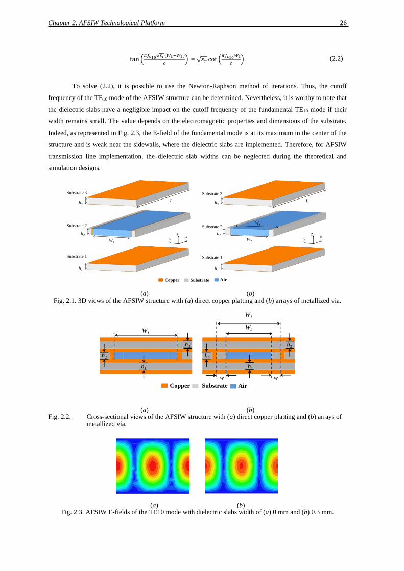
Chapter 2. AFSIW Technological Platform 26
tan (𝜋𝑓c10√ 𝑟(𝑊1−𝑊2)
𝑐) = √𝜀𝑟 cot (
𝜋𝑓c10𝑊2
𝑐). (2.2)
To solve (2.2), it is possible to use the Newton-Raphson method of iterations. Thus, the cutoff
frequency of the TE10 mode of the AFSIW structure can be determined. Nevertheless, it is worthy to note that
the dielectric slabs have a negligible impact on the cutoff frequency of the fundamental TE10 mode if their
width remains small. The value depends on the electromagnetic properties and dimensions of the substrate.
Indeed, as represented in Fig. 2.3, the E-field of the fundamental mode is at its maximum in the center of the
structure and is weak near the sidewalls, where the dielectric slabs are implemented. Therefore, for AFSIW
transmission line implementation, the dielectric slab widths can be neglected during the theoretical and
simulation designs.
(a) (b) Fig. 2.1. 3D views of the AFSIW structure with (a) direct copper platting and (b) arrays of metallized via.
(a) (b) Fig. 2.2. Cross-sectional views of the AFSIW structure with (a) direct copper platting and (b) arrays of
metallized via.
(a) (b) Fig. 2.3. AFSIW E-fields of the TE10 mode with dielectric slabs width of (a) 0 mm and (b) 0.3 mm.
Substrate 3
Substrate 2
Substrate 1
h3L
W1
Copper Substrate Air
zx
y
h2
h1
h3L
W2
h2
h1
W1
Substrate 3
Substrate 2
Substrate 1
zx
y
W1
W2
w w
W1
Copper Substrate Air
h2
h1
h3 h3
h1
h2

Chapter 2. AFSIW Technological Platform 27
To detail the impact of the dielectric slabs on the AFSIW performances, a study of the unloaded
Q-factor of an AFSIW cavity is presented. As it is stated in [3], the unloaded Q-factor of a resonator defines
the sharpness of the resonance curve. It is defined as:
Qu= 𝜔0
𝑊𝑇
𝑃loss, (2.3)
where WT is the average energy stored in the resonator, Ploss is the power dissipated in the resonator, and ω0 is
the radian resonance frequency. The power dissipated in the resonator is the sum of the power dissipated in the
conducting walls Pc and the power dissipated in the dielectric Pd. Hence, the unloaded Q-factor can be
rearranged into:
1
Qu
=1
Q𝑐
+ 1
Q𝑑
, (2.4)
where Qc = ω0WT/Pc and Qd = ω0WT/Pd.
The study is based on the eigenmode simulations of the EM software ANSYS HFSS with copper as
conductive metal. Two AFSIW cavities, implementing continuous sidewalls (directly copper platted) and
discontinuous sidewalls (arrays of metallized via), respectively, are compared in terms of unloaded Q-factor.
Both cavities, represented in Fig. 2.4 have a fixed width W1 = 13 mm and the length L is adjusted so the cavity
resonates at 21 GHz. Rogers RT/Duroid 6002 material, with a permittivity of 2.94 and a tanδ of 0.0012, is used
for the particular case of discontinuous sidewalls. The diameter d of the vias is 0.4 mm and the distance between
two center-to-center consecutive vias p is 0.8 mm. It can be observed in Fig. 2.5 that the unloaded Q-factor
varies from 2496 (with w = 0 mm) to 2453 (with w = 0.4 mm), 1438 (with w = 0 mm) to 1415 (with
w = 0.4 mm), 1005 (with w = 0 mm) to 995 (with w = 0.4 mm), for PCB standard thickness of 1.524 mm,
0.762 mm, and 0.508 mm, respectively. Therefore, it can be concluded that the dielectric slabs can be neglected
in the design of such component. Moreover, if the dielectric slabs are not used to achieve a specific electric
function, there is no need to implement them.
(a) (b) Fig. 2.4. Top views of AFSIW cavities implementing (a) direct copper platting and (b) arrays of
metallized via.
Copper Substrate Air
Metallized vias
L
W1W1
L
wd p

Chapter 2. AFSIW Technological Platform 28
Fig. 2.5. Eigenmode simulations of the unloaded Q-factor of an AFSIW cavity loaded with dielectric slabs (width w) with different PCB standard thickness.
2. 2. Air-Filled Substrate Integrated Waveguide Transmission
Line
To evaluate the intrinsic performances of the AFSIW technology, the simplest component to study is a
transmission line. In this section, theoretical analyses, simulations using ANSYS HFSS electromagnetic (EM)
software, and measurement results are presented. Due to the foreseen interest of the AFSIW technological
platform for space applications, the proposed transmission line is studied and demonstrated in the Ka-band
satellite communication frequency range (17.3 to 21.3 GHz) which is included in the WR-51 band. First, the
loss mechanism in an AFSIW transmission line is briefly explained. Then, a transition from conventional
rectangular waveguide (RWG) to AFSIW is detailed. This transition is then used in a test fixture to characterize
an AFSIW transmission line. Finally, power-handling tests on the proposed component are carried out to
evaluate the behavior of the technology.
2. 2. 1 Loss Mechanism
The AFSIW, as any propagation technology, is subjected to losses. Those losses impact the performance of the
propagating structure and is an important aspect to consider. They can be classified into three categories, the
conductor losses, dielectric losses, and radiation losses. The total attenuation α is expressed as:
𝛼 = 𝛼𝑑 + 𝐾 ∗ 𝛼𝑐+𝛼𝑟. (2.3)
0 0.1 0.2 0.3 0.40
1000
2000
3000
w (mm)
Un
load
ed Q
-fa
cto
r
1.524 mm thickness
0.762 mm thickness
0.508 mm thickness
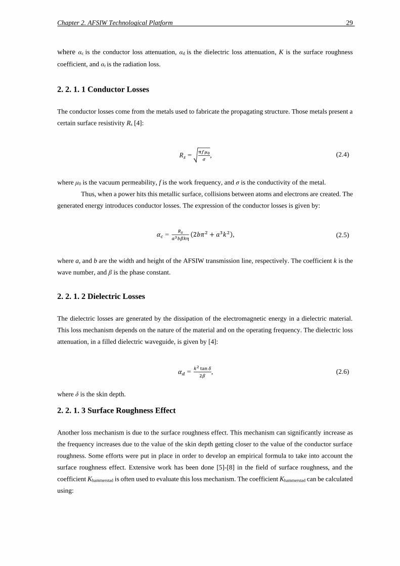
Chapter 2. AFSIW Technological Platform 29
where αc is the conductor loss attenuation, αd is the dielectric loss attenuation, K is the surface roughness
coefficient, and αr is the radiation loss.
2. 2. 1. 1 Conductor Losses
The conductor losses come from the metals used to fabricate the propagating structure. Those metals present a
certain surface resistivity Rs [4]:
𝑅𝑠 = √π𝑓𝜇0
𝜎, (2.4)
where μ0 is the vacuum permeability, f is the work frequency, and σ is the conductivity of the metal.
Thus, when a power hits this metallic surface, collisions between atoms and electrons are created. The
generated energy introduces conductor losses. The expression of the conductor losses is given by:
𝛼𝑐 = 𝑅𝑠
𝑎3𝑏𝛽𝑘η(2𝑏𝜋2 + 𝑎3𝑘2), (2.5)
where a, and b are the width and height of the AFSIW transmission line, respectively. The coefficient k is the
wave number, and β is the phase constant.
2. 2. 1. 2 Dielectric Losses
The dielectric losses are generated by the dissipation of the electromagnetic energy in a dielectric material.
This loss mechanism depends on the nature of the material and on the operating frequency. The dielectric loss
attenuation, in a filled dielectric waveguide, is given by [4]:
𝛼𝑑 = 𝑘2 tan 𝛿
2𝛽, (2.6)
where δ is the skin depth.
2. 2. 1. 3 Surface Roughness Effect
Another loss mechanism is due to the surface roughness effect. This mechanism can significantly increase as
the frequency increases due to the value of the skin depth getting closer to the value of the conductor surface
roughness. Some efforts were put in place in order to develop an empirical formula to take into account the
surface roughness effect. Extensive work has been done [5]-[8] in the field of surface roughness, and the
coefficient Khammerstad is often used to evaluate this loss mechanism. The coefficient Khammerstad can be calculated
using:

Chapter 2. AFSIW Technological Platform 30
𝐾𝐻𝑎𝑚𝑚𝑒𝑟𝑠𝑡𝑎𝑑 = 1+2
𝜋(1.4 ∗ (
𝐻𝑟𝑚𝑠
𝛿)), (2.7)
where Hrms is the root mean square (RMS) conductor.
2. 2. 1. 4 Radiation Losses
In the particular case of this thesis, the components based on AFSIW with continuous sidewalls are
self-shielded thanks to the structure of the technology. For the case of discontinuous sidewalls, the distance
between two consecutive vias is small enough to neglect the radiation losses as it is demonstrated in [9], [10].
Thus, the radiation losses in both cases are considered null. Hence the total attenuation α becomes:
𝛼 = 𝛼𝑑 + 𝐾𝐻𝑎𝑚𝑚𝑒𝑟𝑠𝑡𝑎𝑑 ∗ 𝛼𝑐. (2.8)
To further highlight the interest of the technology as a propagation medium, a previous thesis has
compared, theoretically and in simulations, the principal characteristics of an AFSIW transmission line
compared to other planar technologies such as microstrip and conventional SIW [11]. The Table 2.1
summarizes the different results. All the technologies were compared with 0.508 mm thick substrates at
33 GHz. However, this frequency band is not the one of interest and thus it is necessary to study the technology
in the desired frequency band. Moreover, in [2] and [11] the technologies are also compared theoretically in
terms of power-handling capability. Nevertheless, this work did not address the power-handling effects linked
to space applications, such as multipactor effect or corona effect, later explained in this Chapter. Hence, the
following Sections will try to fill in the blanks of the AFSIW technology.
TABLE 2.1
SUMMARY OF THEORETICAL TOTAL LOSS FOR DIFFERENT TRANSMISSION LINE TECHNOLOGIES
Technology Microstrip SIW SIW AFSIW
Substrate Rogers 5880 Rogers 5880 Rogers 6002 Rogers 6002
Total loss (dB/cm) 0.073 0.095 0.13 0.033
2. 2. 2. AFSIW to RWG Transition
To be able to characterize intrinsically the technology in terms of electrical performances, power-handling and
thermal behavior, a transition from standard RWG to AFSIW must be designed. Hence, a compact five-section
height-stepped RWG to AFSIW is detailed. The standard RWG section allows characterizing AFSIW circuits
as this type of transition is not the limiting part, contrary to PCB integrated solutions.
The proposed transition is illustrated in Fig. 2.6. The AFSIW circuits can be seen as a nonstandard
RWG. Thus, to design the transition, the easiest solution is to make a gradual change of section on several
wavelengths. This solution is very costly, bulky, and not compact. To overcome those disadvantages, the
transition can be designed using a series of discontinuities separated by a quarter-wavelength. This type of
stepped impedance transformer has a wide bandwidth, as it keeps the same width while lowering the height.
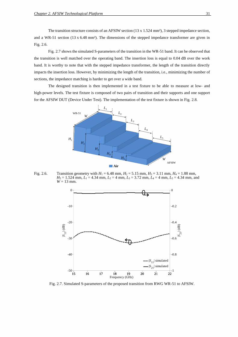
Chapter 2. AFSIW Technological Platform 31
The transition structure consists of an AFSIW section (13 x 1.524 mm²), 3 stepped impedance section,
and a WR-51 section (13 x 6.48 mm²). The dimensions of the stepped impedance transformer are given in
Fig. 2.6.
Fig. 2.7 shows the simulated S-parameters of the transition in the WR-51 band. It can be observed that
the transition is well matched over the operating band. The insertion loss is equal to 0.04 dB over the work
band. It is worthy to note that with the stepped impedance transformer, the length of the transition directly
impacts the insertion loss. However, by minimizing the length of the transition, i.e., minimizing the number of
sections, the impedance matching is harder to get over a wide band.
The designed transition is then implemented in a test fixture to be able to measure at low- and
high-power levels. The test fixture is composed of two pairs of transition and their supports and one support
for the AFSIW DUT (Device Under Test). The implementation of the test fixture is shown in Fig. 2.8.
Fig. 2.6. Transition geometry with H1 = 6.48 mm, H2 = 5.15 mm, H3 = 3.11 mm, H4 = 1.88 mm, H5 = 1.524 mm, L1 = 4.34 mm, L2 = 4 mm, L3 = 3.72 mm, L4 = 4 mm, L5 = 4.34 mm, and W = 13 mm.
Fig. 2.7. Simulated S-parameters of the proposed transition from RWG WR-51 to AFSIW.
AFSIW
WR-51
H1
H2
H3
H4
H5
L1
L2
L3
L4
L5
W
W
Air
15 16 17 18 19 20 21 22-50
-40
-30
-20
-10
0
|S11| (
dB
)
Frequency (GHz)
→
15 16 17 18 19 20 21 22-1
-0.8
-0.6
-0.4
-0.2
0
|S21| (
dB
)
|S11
| simulated
|S21
| simulated

Chapter 2. AFSIW Technological Platform 32
Fig. 2.8. 3D view of the proposed test fixture.
2. 2. 3. AFSIW Transmission Line
Based on Section 2. 1, an AFSIW transmission line is designed. To be able to operate in the WR-51 band, the
AFSIW transmission line has a width of 13 mm, the height of the transmission line is chosen to be one of the
PCB standard height, h2 = 1.524 mm, and is equal to the AFSIW section height.
To be able to have the optimal performances, the electrical sidewalls of the transmission line were
chosen to be copper platted. Hence, the dielectric losses are null and the AFSIW transmission line is similar to
a WR-51 waveguide with a smaller height.
It is then possible to evaluate the principal characteristics of the AFSIW transmission line using the
previous given formulas. With the chosen dimensions, the cutoff frequency of the TE10 mode is equal to
11.57 GHz using (2.1). Then, the lowest frequency band, which corresponds to 1.25*fc10 in order to avoid the
high dispersive region occurring near the cutoff frequency [12], is equal to 14.46 GHz.
For demonstration purposes, an AFSIW transmission line is implemented using 1.524 mm thick Hi-Tg
FR4 substrate for the three layers of the PCB. The transmission line has a length L = 70 mm and a width
W = 13 mm. The fabricated inner substrate is shown in Fig. 2.9. Measurements were made using a N5225A
PNA microwave network analyzer from Keysight with the WR-51 test fixture introduced previously. The
effects of the cables, WR-51 waveguide and test fixture are de-embedded using a thru-reflect-line (TRL)
AFSIW calibration kit. The AFSIW TRL kit has been designed and fabricated following the procedure
explained in [14]. Reference planes are shown in Fig. 2.9. The theoretical, simulated, and measured
transmission loss for the proposed structure is compared in Fig. 2.10. The theoretical loss mechanism of the
AFSIW transmission line was calculated using (2.5) – (2.7) with a Hrms of 0.6 µm. Fig. 2.10 shows that the
measured transmission loss varies from 0.02 dB/cm to 0.01 dB/cm over the band. The observed oscillation for
the measured results comes from the incertitude of the TRL calibration. It can also be observed from Fig. 2.11
that the return loss of the fabricated AFSIW transmission line remains greater than 20 dB over the work band,
Support of the
transition
Transition
Base plateDUT
Support of the
DUTCutting view of
the transition

Chapter 2. AFSIW Technological Platform 33
which demonstrates the good electrical behavior of the transmission line. To measure the transmission line, the
test fixture previously presented is used. A photograph is given in Fig. 2.12.
Fig. 2.9. Fabricated inner substrate of the AFSIW transmission line.
2. 2. 4. AFSIW Transmission Line Power-Handling
For microwave applications, it is important to evaluate the power-handling capability of a technology.
Depending on the application, especially for space applications, the power limitation in terms of continuous
wave signal can be a limiting effect. In a payload, interconnections between different components can be
achieved using transmission line sections. Thus, evaluating the power-handling of an AFSIW transmission line
can be useful for future implementations.
Therefore, to validate the power-handling capability of the AFSIW transmission line, experimental
tests are carried out using Cobham Microwave high-power facilities. The experimental setup is shown in
Fig. 2.13. To fully characterize the technology for space applications, the power-handling test is made using
space environment conditions. Therefore, the DUT is placed in a vacuum chamber. The test flow is described
below. First part of the test consists in reaching the partial vacuum (~10-5 mbar). This level of pressure is lower
than the one requested for conventional tests under vacuum [13]. Once this pressure is established, the input
power level is increased until the maximum power level available in Cobham facilities (190 W) in this
frequency band. Then, the temperature in the vacuum chamber is increased to reach 90 °C. A higher
temperature allows placing the DUT in a more stringent environment, as the conductivity of the metals and the
electrical performances are degraded. Finally, the component behavior is observed in these conditions for a
sufficient amount of time.
Reference planes

Chapter 2. AFSIW Technological Platform 34
Fig. 2.10. Transmission loss of an AFSIW transmission line obtained in theory, simulation, and measurement.
Fig. 2.11. Measured S-parameters of the AFSIW transmission line of length 70 mm.
17.3 18.3 19.3 20.3 21.30
0.01
0.02
0.03
0.04
Frequency (GHz)
Tra
nsm
issi
on
Lo
ss (
dB
/cm
)
Theory
Simulation
Measurement
17.3 18.3 19.3 20.3 21.3-50
-40
-30
-20
-10
0
|S11| (
dB
)
Frequency (GHz)
→
17.3 18.3 19.3 20.3 21.3-1
-0.8
-0.6
-0.4
-0.2
0
|S21| (
dB
)
|S11
| measured
|S21
| measured

Chapter 2. AFSIW Technological Platform 35
Fig. 2.12. Photographs of the AFSIW transmission line on the proposed test fixture.
The power-handling test is made at a single frequency point, here 20.9 GHz. It can be observed from
Fig. 2.14 that the return loss of the transmission line remains greater than 20 dB during the whole test, thus
demonstrating the good behavior of the component. Fig. 2.15 and Fig. 2.16 shows the behavior of the DUT in
pressure and temperature. It can be observed in Fig. 2.15, that the pressure increases as the temperature is
increased. This phenomenon is very current in the power-handling test under vacuum conditions and is called
outgassing.
The power-handling test is well performed, and no sign of large decrease of return loss, large
unexpected rapid decrease or increase of the temperature (except the ones created by power or thermal
modifications) are observed. Thus, it can be concluded that the AFSIW transmission line can handle a minimum
of 190 W under vacuum condition with a thermal set point of 90 °C.
Fig. 2.13. Setup of the power-handling test with CW input in the vacuum chamber (10-5 mbar).
AFSIW
Transmission Line
AFSIW to WR-51
Transition
WR-51 Adapter
RF signal
generatorDUT
Po
wer
senso
r
Po
wer
senso
r
Power
meter
Power
meter
Vacuum Chamber
ReverseForward
Thermal sensor
LoadCross coupler
Isolator
Load
Po
wer
senso
r
Power
meter
Forward Load

Chapter 2. AFSIW Technological Platform 36
Fig. 2.14. Measured CW input power and return loss over time of the AFSIW transmission line in the vacuum chamber (10-5 mbar) at 20.9 GHz.
Fig. 2.15. Measured CW input power and pressure over time of the AFSIW transmission line in the vacuum chamber (10-5 mbar) at 20.9 GHz.
0 1000 2000 3000 4000 5000 6000 70000
20
40
60
80
100
120
140
160
180
200
Co
nti
nu
ou
s W
ave
Inp
ut
Po
wer
(W
)
Time (s)
→
0 1000 2000 3000 4000 5000 6000 7000-50
-40
-30
-20
-10
0
|S11| (
dB
)
Input power
|S11
|
0 1000 2000 3000 4000 5000 6000 70000
20
40
60
80
100
120
140
160
180
200
Co
nti
nu
ou
s W
ave
Inp
ut
Po
wer
(W
)
Time (s)
→
0 1000 2000 3000 4000 5000 6000 70001
2
3
4
5
6
7
8
9
10
Pre
ssu
re (
10-5
mB
ar)
Input power
Pressure in vacuum chamber

Chapter 2. AFSIW Technological Platform 37
Fig. 2.16. Measured CW input power and temperature over time of the AFSIW transmission line in the vacuum chamber (10-5 mbar) at 20.9 GHz.
2. 3. Air-Filled Substrate Integrated Waveguide Filter
In the past decades, the emerging telecommunication applications such as telemetry, navigation, and remote
control have tremendously stimulated the development of novel microwave and millimeter-wave components.
The future generation of RF front-end, and payload systems have pushed the community to pursue high
performance, high selectivity, low insertion loss, high power-handling performances. Among the microwave
components, microwave filters have a crucial role in the communication chain.
A microwave filter is a two-port network component used to select a specific frequency band while
rejecting other frequency bands. One of the crucial parameters of a filter technology is the Q-factor as it defines
the achievable insertion loss. A promising feature of the AFSIW technology is to benefit from a high Q-factor
while maintaining a high integration degree at a low cost. Microwave AFSIW filters can be synthesized by
using classic design procedures for the conventional air-filled waveguide filters. Thus, the synthesis of AFSIW
filters is similar to the synthesis of air-filled waveguide filters, although the sidewalls of an AFSIW can be
implemented by using arrays of metallized via. In order to alleviate the time of simulation and to be able to use
well-known synthesis methodologies, the sidewalls are often implemented as perfect electric conductors (PEC)
in the simulation tools. Once the design is completed, it is possible, depending on the application, to implement
the arrays of metallized via in order to fully simulate the total structure.
0 1000 2000 3000 4000 5000 6000 70000
20
40
60
80
100
120
140
160
180
200
Co
nti
nu
ou
s W
ave
Inp
ut
Po
wer
(W
)
Time (s)
→
0 1000 2000 3000 4000 5000 6000 70000
20
40
60
80
100
120
140
Tem
per
atu
re (
°C)
0 1000 2000 3000 4000 5000 6000 70000
20
40
60
80
100
120
140
Input power
Temperature on DUT
Temperature in the chamber
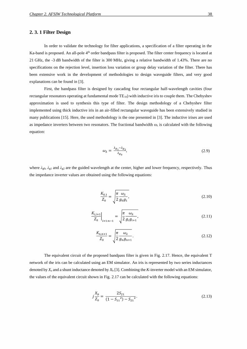
Chapter 2. AFSIW Technological Platform 38
2. 3. 1 Filter Design
In order to validate the technology for filter applications, a specification of a filter operating in the
Ka-band is proposed. An all-pole 4th order bandpass filter is proposed. The filter center frequency is located at
21 GHz, the -3 dB bandwidth of the filter is 300 MHz, giving a relative bandwidth of 1.43%. There are no
specifications on the rejection level, insertion loss variation or group delay variation of the filter. There has
been extensive work in the development of methodologies to design waveguide filters, and very good
explanations can be found in [3].
First, the bandpass filter is designed by cascading four rectangular half-wavelength cavities (four
rectangular resonators operating at fundamental mode TE10) with inductive iris to couple them. The Chebyshev
approximation is used to synthesis this type of filter. The design methodology of a Chebyshev filter
implemented using thick inductive iris in an air-filled rectangular waveguide has been extensively studied in
many publications [15]. Here, the used methodology is the one presented in [3]. The inductive irises are used
as impedance inverters between two resonators. The fractional bandwidth ωλ is calculated with the following
equation:
𝜔𝜆 = 𝜆𝑔1
−𝜆𝑔2
𝜆𝑔0
, (2.9)
where λg0, λg1 and λg2 are the guided wavelength at the center, higher and lower frequency, respectively. Thus
the impedance inverter values are obtained using the following equations:
𝐾0,1𝑍0
= √𝜋
2
𝜔𝜆
𝑔0𝑔1, (2.10)
𝐾𝑖,𝑖+1𝑍0
|𝑖=1:𝑛−1
= √𝜋
2
𝜔𝜆
𝑔𝑖𝑔𝑖+1, (2.11)
𝐾𝑛,𝑛+1𝑍0
= √𝜋
2
𝜔𝜆
𝑔𝑛𝑔𝑛+1. (2.12)
The equivalent circuit of the proposed bandpass filter is given in Fig. 2.17. Hence, the equivalent T
network of the iris can be calculated using an EM simulator. An iris is represented by two series inductances
denoted by Xa and a shunt inductance denoted by Xb [3]. Combining the K-inverter model with an EM simulator,
the values of the equivalent circuit shown in Fig. 2.17 can be calculated with the following equations:
𝑗𝑋𝑏𝑍0
= 2𝑆21
(1 − 𝑆11²) − 𝑆21². (2.13)

Chapter 2. AFSIW Technological Platform 39
𝑗𝑋𝑎𝑍0
= 1 + 𝑆11 − 𝑆211 − 𝑆11 + 𝑆21
, (2.14)
where S11 and S21 are the S-parameters of the dominant TE10 mode. The values Xa and Xb are related to K and
ϕ as follows:
𝐾
𝑍0= |tan (
𝜙
2+ tan−1
𝑋𝑏𝑍0)| , (2.15)
𝜙 = − tan−1 (2𝑋𝑎𝑍0
+𝑋𝑏𝑍0) − tan−1
𝑋𝑏𝑍0
. (2.16)
These functions are not explicit, and it is necessary to run the EM simulator for a range of iris widths
to calculate S-parameters of the corresponding Xa, Xb, K, and ϕ. Knowing the value for K, it is possible to find
the corresponding iris width. Then, the corresponding value ϕ is used to find the resonators’ lengths using:
𝑙𝑖 =𝜆𝑔0
2𝜋(𝜋 +
1
2(𝜙𝑖 + 𝜙𝑖+1)) . (2.17)
The methodology is used to design an all-pole fourth-order bandpass filter. The structure and the
dimensions of the bandpass filter are shown in Fig. 2.18. The thickness of the inductive iris is fixed to 2 mm.
As the proposed filter function is basic, the dielectric slabs were not required in this case, hence the electric
sidewalls are directly implemented by copper platting. It is important to add that the filter is symmetric,
meaning dimensions of cavities 1, 4, and cavities 2, 3 are equal (L1 = L4, L2 = L3). Obviously, the inductive iris
follows the same logic.
Fig. 2.17. Equivalent circuit of the proposed bandpass filter.
𝑋𝑎1 𝑋𝑎1
𝑋𝑏1
1𝑋𝑎2 𝑋𝑎2
𝑋𝑏2
2𝑋𝑎3 𝑋𝑎3
𝑋𝑏3
3𝑋𝑎 𝑋𝑎
𝑋𝑏
𝑋𝑎 𝑋𝑎
𝑋𝑏
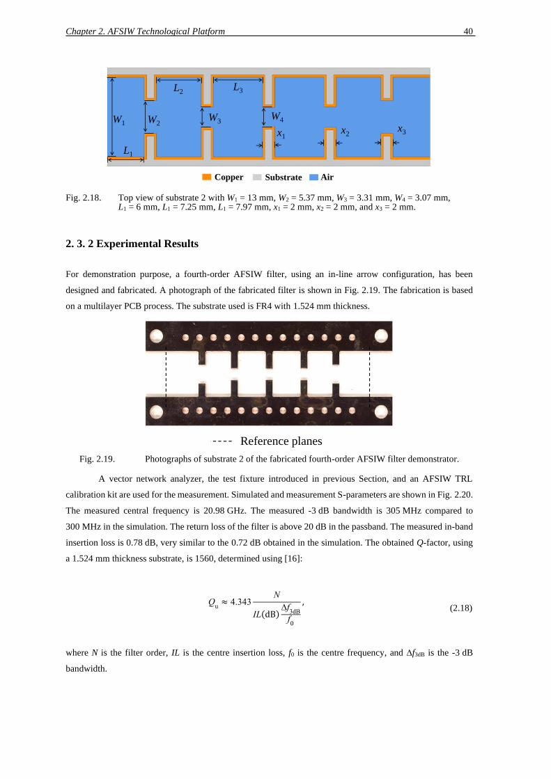
Chapter 2. AFSIW Technological Platform 40
Fig. 2.18. Top view of substrate 2 with W1 = 13 mm, W2 = 5.37 mm, W3 = 3.31 mm, W4 = 3.07 mm, L1 = 6 mm, L1 = 7.25 mm, L1 = 7.97 mm, x1 = 2 mm, x2 = 2 mm, and x3 = 2 mm.
2. 3. 2 Experimental Results
For demonstration purpose, a fourth-order AFSIW filter, using an in-line arrow configuration, has been
designed and fabricated. A photograph of the fabricated filter is shown in Fig. 2.19. The fabrication is based
on a multilayer PCB process. The substrate used is FR4 with 1.524 mm thickness.
Fig. 2.19. Photographs of substrate 2 of the fabricated fourth-order AFSIW filter demonstrator.
A vector network analyzer, the test fixture introduced in previous Section, and an AFSIW TRL
calibration kit are used for the measurement. Simulated and measurement S-parameters are shown in Fig. 2.20.
The measured central frequency is 20.98 GHz. The measured -3 dB bandwidth is 305 MHz compared to
300 MHz in the simulation. The return loss of the filter is above 20 dB in the passband. The measured in-band
insertion loss is 0.78 dB, very similar to the 0.72 dB obtained in the simulation. The obtained Q-factor, using
a 1.524 mm thickness substrate, is 1560, determined using [16]:
Qu≈ 4.343
N
IL(dB)∆f
3dB
f0
, (2.18)
where N is the filter order, IL is the centre insertion loss, f0 is the centre frequency, and ∆f3dB is the -3 dB
bandwidth.
Copper Substrate Air
W1 W2
L2
x2
W3
L3
L1
x1
L4
W5
x4 x5
dx
dy
Metallized vias
Inductive iris
x6
W4
x3
Reference planes

Chapter 2. AFSIW Technological Platform 41
Fig. 2.20. Simulated and measured S-parameters of the in-line 4th order AFISW filter.
2. 3. 3. AFSIW Filter Power-Handling
For high-power operations, different effects must be taken into account. The first one is related to the thermal
aspect and high-power breakdown, it is usually evaluated using a continuous wave test. The second one is the
multipaction breakdown. Finally, the ionization breakdown, also known as corona effect, can also be
detrimental in such applications. These different effects are evaluated for the AFSIW technological platform
on the previously measured AFSIW filter demonstrator. It is worthy to add that another effect called passive
intermodulation (PIM) is also important but is not studied in this work. The multipactor and corona tests were
not performed on the AFSIW transmission line as it is not often a component subjected to those effects.
2. 3. 3. 1 Continuous Wave Test
To validate the power-handling capability of the AFSIW filter, experimental tests are carried out using Cobham
Microwave high-power facilities. The experimental setup is the same as the one presented in Section 2. 2. 4.
The test flow is similar to the one in the transmission line section except that the temperature of the vacuum
chamber is not increased. Indeed, a filter is usually more lossy than a transmission line, operating at the same
frequency and fabricated with the same technology. Under high-power conditions, those losses are responsible
for a self-heating. Thus, to study the behavior of the filter, the temperature in the vacuum chamber was not
increased.
20 20.5 21 21.5 22-50
-40
-30
-20
-10
0
Frequency (GHz)
|Sij| (
dB
)
|S11
| simulated
|S11
| measured
|S21
| simulated
|S21
| measured

Chapter 2. AFSIW Technological Platform 42
The test is made at 20.9 GHz. Fig. 2.21 shows that the return loss of the filter remains greater than
20 dB during the time of the test. It is shown from Fig. 2.21 that the return loss is increasing during the test.
As the temperature of the DUT is increasing, the physical dimensions of the filter expand causing the filter
response to shift in frequency. As the test is performed on a single frequency point, the value of the RL is
susceptible to change. This variation is continuous and shows no rapid change demonstrating the correct
behavior of the component. It can be observed from Fig. 2.22 that the pressure of the test is 10-5 mbar during
the whole test. Fig. 2.23 shows the input power, the temperature of the DUT and vacuum chamber versus time.
As explained previously, it was not necessary to regulate the temperature in the vacuum chamber as the filter
reach high temperature (120 °C) due to the losses. The filter is pressed on a brass support and the thermal
sensor is placed on the top of the DUT.
It is demonstrated from the different responses that there is no sign of large decrease of return loss,
large unexpected decrease or increase of any temperature (except the ones created by power or thermal
modifications) are observed. Thus, it can be concluded that the AFSIW filter can handle a minimum of 190 W
under vacuum condition. It is also worthy to observe that the filter behaves correctly with a measured stabilized
temperature of 120 °C.
Fig. 2.21. Measured CW input power and return loss over time of the 4th order AFSIW filter in the
vacuum chamber at 20.9 GHz.
0 1000 2000 3000 4000 5000 6000 70000
20
40
60
80
100
120
140
160
180
200
Co
nti
nu
ou
s W
ave
Inp
ut
Po
wer
(W
)
Time (s)
→
0 1000 2000 3000 4000 5000 6000 7000-50
-40
-30
-20
-10
0
|S11| (
dB
)
Input power
|S11
|

Chapter 2. AFSIW Technological Platform 43
Fig. 2.22. Measured CW power and pressure return loss over time of the 4th order AFSIW filter in the
vacuum chamber at 20.9 GHz.
Fig. 2.23. Measured CW input power and temperature over time of the 4th order AFSIW filter in the
vacuum chamber at 20.9 GHz.
0 1000 2000 3000 4000 5000 6000 70000
20
40
60
80
100
120
140
160
180
200
Co
nti
nu
ou
s W
ave
Inp
ut
Po
wer
(W
)
Time (s)
→
0 1000 2000 3000 4000 5000 6000 70000
1
2
3
4
5
6
7
8
9
10
Pre
ssu
re (
10-5
mB
ar)
Input power
Pressure in vacuum chamber
0 1000 2000 3000 4000 5000 6000 70000
20
40
60
80
100
120
140
160
180
200
Co
nti
nu
ou
s W
ave
Inp
ut
Po
wer
(W
)
Time (s)
→
0 1000 2000 3000 4000 5000 6000 70000
20
40
60
80
100
120
140
Tem
per
atu
re (
°C)
0 1000 2000 3000 4000 5000 6000 70000
20
40
60
80
100
120
140
Input power
Temperature on DUT
Temperature in the chamber

Chapter 2. AFSIW Technological Platform 44
2. 3. 3. 2 Multipactor Test
Multipactor breakdown is an electron avalanche discharge, happening under vacuum conditions and
high-power RF electromagnetic fields [17]. This phenomenon can occur in satellite passive communication
devices. The RF electromagnetic fields are susceptible to accelerate free electrons inside the component, those
electrons, striking the metallic surfaces of the component can release secondary electrons. By a phenomenon
of avalanche-like, a high electrical current can be created between the metallic surfaces, thus creating a short-
circuit canceling the component function. Extensive work has been made to study the multipactor effect [18]
and the intent of this thesis is to evaluate the power level the AFSIW technology can reach.
The interaction between the electron and the metallic surface can be modeled with the SEY
(Secondary Electron Yield) function. The SEY model and formulas are described in [19] and [20]. Using the
different data, a simulation of the multipactor effect was carried out using the software SPARK3D. The
simulation shows no multipactor effect, using as input power the maximum available power in Cobham
facilities (190 W).
In order to validate the simulation, an experimental test is carried out using Cobham Microwave high-
power facilities. The experimental setup is shown in Fig. 2.24 and is the conventional one for multipactor
measurements. A photograph of the electron gun position is given in Fig. 2.25. Contrary to the continuous
wave input power-handling test, the multipactor test is made using pulsed input power in order to lower the
self-heating of the filter. The applied signal has been pulsed with a carrier frequency of 20.9 GHz, a pulse
width of 100 μs with a duty cycle of 10%. The pressure of the vacuum chamber is set at 5.5 10-6 mbar. Fig. 2.26
shows the return loss of the filter over the time range. It can be observed that the return loss is above 20 dB.
Fig. 2.27 presents the pulsed input power, temperature of the DUT and vacuum chamber versus time.
To be sure to ignite the multipactor effect, if it is meant to occur, an electron gun is used during the
test to saturate the gap of the two metal plates (critical multipactor area) in electrons. This electron gun needs
to be pointed to a hole where the E-field is at its maximum, in our case, in the center of a resonance cavity. It
is demonstrated from the different tests that there is no sign of large rapid increase or decrease of return loss
or temperature. Thus, it can be concluded that the AFSIW filter can handle 190 W without multipactor effect
occurring.
Fig. 2.24. Setup of the multipactor test with the detection systems.
RF signal
generatorDUT
Po
wer
senso
r
Po
wer
senso
r
Power
meter
Power
meter
Vacuum chamber
ReverseForward
Electron gun
LoadCross coupler
Isolator
Load
Atten
uato
r
Ph
ase
Sh
ifter
Splitter
Spectrum
Analyzer
Splitter
Peak Power
Analyzer
Po
wer
senso
r
Power
meter

Chapter 2. AFSIW Technological Platform 45
Fig. 2.25. Photographs of the multipactor test with the electron gun pointed to the DUT.
Fig. 2.26. Measured pulsed input power and return loss over time of the 4th order AFSIW filter in the
vacuum chamber at 20.9 GHz.
0 1000 2000 3000 4000 5000 6000 70000
20
40
60
80
100
120
140
160
180
200
Pu
lsed
In
pu
t P
ow
er (
W)
Time (s)
→
0 1000 2000 3000 4000 5000 6000 7000-50
-40
-30
-20
-10
0
|S11| (
dB
)
Input power
|S11
|

Chapter 2. AFSIW Technological Platform 46
Fig. 2.27. Measured pulsed input power and temperature over time of the 4th order AFSIW filter in the
vacuum chamber at 20.9 GHz.
2. 3. 3. 3 Corona Test
A corona discharge is an electrical discharge involving electron dynamics inside gases. When the electric field
is strong enough, a chain reaction can be created. Electrons in the air can ionize atoms by colliding with them
with enough energy transfer, resulting in releasing other electrons. Those electrons are susceptible to have the
same behavior and thus create an avalanche-like reaction. To be able to ionize the two major constituents of
air (N2 and O2), it is necessary to have high electric fields. If the avalanche-like process is ignited, it results in
the formation of an electron plasma. This electron plasma is synonymous with a corona discharge and is a
destructive phenomenon.
The AFSIW technology presents an important density of the electric field due to the small thickness
of the substrates involved and the achieved Q-factor. Thus, filters using this technology are susceptible to
present a corona discharge for high power applied signals. Ionization breakdown in microwave filters is an
extremely complicated phenomenon to analyze. As for the other tests, the intent of this work is to present the
results of the corona test. Readers are encouraged to consult the references that cover in more details the
phenomenon [21]-[24].
To evaluate the input power and the critical pressure susceptible to create a corona discharge, the
E-fields of the AFSIW filter are extracted from the EM simulator and inserted in the SPARK3D simulator.
From SPARK3D, the critical pressure is evaluated as 26 mbar and a corona discharge occurs at 11 W. The
critical pressure is the pressure at which the component has the lowest power-handling capability. The critical
pressure is linked to the Paschen’s law.
Therefore, to validate the simulated results, a corona test has been performed using Cobham
Microwave high-power facilities. Fig. 2.28 shows a schematic diagram of the measurement setup. In this test,
0 1000 2000 3000 4000 5000 6000 70000
20
40
60
80
100
120
140
160
180
200
Pu
lsed
In
pu
t P
ow
er (
W)
Time (s)
→
0 1000 2000 3000 4000 5000 6000 70000
20
40
60
80
100
120
140
Tem
per
atu
re (
°C)
0 1000 2000 3000 4000 5000 6000 70000
20
40
60
80
100
120
140
Input power
Temperature on DUT
Temperature in the chamber

Chapter 2. AFSIW Technological Platform 47
a conventional method consisting in observing the RL behavior has been employed to detect corona discharge.
The procedure for test consists in establishing the desired input power, then decrease the pressure until reaching
the critical pressure, observe the DUT behavior for 30 minutes, then decrease again the pressure until
3 10-5 mbar, and finally observe the DUT behavior.
The input power was set to 9 W with a carrier frequency of 20.9 GHz. In Fig. 2.29 and Fig. 2.30, the
measured return loss and temperature on the DUT are shown. As previously explained, it can be observed that
the pressure is decreased from 1015 mbar to 26 mbar (critical pressure) at 451 s, and from 26 mbar to
3 10-5 mbar at 2100 s, as it is shown in Fig. 2.31. During the test, Fig 2.29 shows that the return loss of the filter
remains greater than 20 dB, and Fig. 2.30 presents a stable temperature on the DUT.
It is demonstrated from the different responses that there is no sign of large decrease of return loss or
temperature. Thus, it can be concluded that the AFSIW filter can handle 9 W at a critical pressure of 26 mbar.
Fig. 2.28. Setup of the corona test.
Fig. 2.29. Measured input power and return loss over time of the 4th order AFSIW filter in the vacuum
chamber at 20.9 GHz.
RF signal
generatorDUT
Po
wer
senso
r
Po
wer
senso
r
Power
meter
Power
meter
Vacuum Chamber
ReverseForward
Thermal sensor
LoadCross coupler
Isolator
Load
Po
wer
senso
r
Power
meter
Forward Load
0 500 1000 1500 2000 2500 30000
5
10
15
20
Co
nti
nu
ou
s W
ave
Inp
ut
Po
wer
(W
)
Time (s)
→
0 500 1000 1500 2000 2500 3000-50
-40
-30
-20
-10
0
|S11| (
dB
)
Input power
|S11
|

Chapter 2. AFSIW Technological Platform 48
Fig. 2.30. Measured input power and temperature over time of the 4th order AFSIW filter in the vacuum
chamber at 20.9 GHz.
Fig. 2.31. Measured input power and pressure over time of the 4th order AFSIW filter in the vacuum
chamber at 20.9 GHz.
0 500 1000 1500 2000 2500 30000
5
10
15
20
Co
nti
nu
ou
s W
ave
Inp
ut
Po
wer
(W
)
Time (s)
→
0 500 1000 1500 2000 2500 30000
10
20
30
Tem
per
atu
re (
°C)
Input power
Temperature on the DUT
0 500 1000 1500 2000 2500 30000
5
10
15
20
Co
nti
nu
ou
s W
ave
Inp
ut
Po
wer
(W
)
Time (s)
→
0 500 1000 1500 2000 2500 30000
500
1000
1500
Pre
ssu
re (
mb
ar)
Input power
Pressure in the chamber

Chapter 2. AFSIW Technological Platform 49
To further investigate on the power handling capability of the fabricated filter, the same test is done
with an input power of 10 W. The measured results are presented in Fig. 2.32 and Fig. 2.34. A large decrease
of the return loss is observed at 685 s and a variation of the temperature on the DUT are observed. The variation
of the temperature is not as pronounced as the return loss variation as the test is automatically stopped when
detecting a variation of RL. If this security was not implemented, the creation of plasma would largely increase
the temperature of the DUT and destroys it. The pressure profile is shown in Fig. 2.35. From the measured
data, it can be concluded that a corona discharge occurs at 26 mbar with an input power of 10 W.
Table 1.2 summarizes the different measured performances obtained for the proposed Ka-band
AFSIW components.
TABLE 1.2
SUMMARY OF MEASURED PERFORMANCES OF THE KA-BAND AFSIW COMPONENTS
Characteristics Transmission Line Filter
Small signal
Return loss (dB) > 20 > 20
Insertion loss (dB) 0.14 0.78
Center frequency (GHz) / 20.98
-3 dB bandwidth (MHz) / 305
-3 dB bandwidth (%) / 1.45
Unloaded Q-factor / 1560
High-power
Continuous wave input power (W) 190 190
Multipactor (W) / 190
Corona (W) @ 26 mbar (free) / 9
Corona (W) @ 26 mbar (sparked) / 10
Fig. 2.32. Measured pulsed input power and pressure over time of the 4th order AFSIW filter in the
vacuum chamber at 20.9 GHz.
0 200 400 600 800 10000
5
10
15
20
Co
nti
nu
ou
s W
ave
Inp
ut
Po
wer
(W
)
Time (s)
→
0 200 400 600 800 1000-50
-40
-30
-20
-10
0
|S11| (
dB
)
Input power
|S11
|

Chapter 2. AFSIW Technological Platform 50
Fig. 2.33. Measured pulsed input power and pressure over time of the 4th order AFSIW filter in the
vacuum chamber at 20.9 GHz.
Fig. 2.34. Measured pulsed input power and pressure over time of the 4th order AFSIW filter in the
vacuum chamber at 20.9 GHz.
0 200 400 600 800 10000
5
10
15
20
Co
nti
nu
ou
s W
ave
Inp
ut
Po
wer
(W
)
Time (s)
→
0 200 400 600 800 10000
10
20
30
Tem
per
atu
re (
°C)
Input power
Temperature on the DUT
0 200 400 600 800 10000
5
10
15
20
Co
nti
nu
ou
s W
ave
Inp
ut
Po
wer
(W
)
Time (s)
→
0 200 400 600 800 10000
500
1000
1500
Pre
ssu
re (
mb
ar)
Input power
Pressure in the chamber

Chapter 2. AFSIW Technological Platform 51
2. 4. Conclusions
In this Chapter, the AFSIW technological platform is introduced. First, the structure of this technology is
detailed as well as the implementation of the electric sidewalls. The loss mechanism of the technology is studied
theoretically and compared to simulations and measurements. To be able to perform power-handling tests, a
transition implemented in a test fixture is developed to be compliant with standard rectangular waveguide
interconnections. To fully characterize the AFSIW transmission line behavior, a CW power-handling test was
performed. The transmission line was tested under vacuum to be as close as possible of the space environment.
The test was successfully done, and it was demonstrated that the AFSIW could handle a 190 W input power at
10-5 mbar for a set temperature of 90 °C. The proposed technology is then used to synthesize a Ka-band all-pole
fourth-order bandpass filter operating at 21 GHz. The fabricated filter presents good results compared to
simulations. To further study the implementation of AFSIW technological platform for filter functions,
power-handling tests, including multipactor test and corona test are performed. The different power tests were
in good agreement with the simulations. For the CW power-handling test, the filter handled a 190 W input
power at 10-5 mbar. The multipactor test showed no multipactor effect with a pulsed input power of 190 °W.
Finally, the corona test presented no corona discharge at a critical pressure of 26 mbar with a CW input power
of 9 W. To evaluate the limit of the technology, another corona test was performed at the same critical pressure
and with a CW input of 10 W, a corona discharge occurred and is closed to the 11 W obtained in the simulation.
The AFSIW technological platform performances in the Ka-band were demonstrated in low- and high-power
signal. In the next Chapter, the versatility of the technology will be discussed as well as the implementation of
standard PCB process.

Chapter 2. AFSIW Technological Platform 52
References
[1] N. Marcuvitz, Waveguide Handbook, Toronto, ON, Canada: McGraw-Hill, 1951, ch. 5, pp. 217-
335.
[2] F. Parment, A. Ghiotto, T. Vuong, J. Duchamp, and K. Wu, “Air-filled substrate integrated
waveguide for low-loss and high power-handling millimeter-wave substrate integrated
circuits,” IEEE Transactions on Microwave Theory and Techniques, vol. 63, no. 4, pp. 1228-1238,
Apr.2015.
[3] R. J. Cameron, C. M. Kudsia, and R. R. Mansour, Microwave Filters for Communication Systems,
Hoboken, NJ, USA: Wiley, 2007, ch. 14, pp. 501-530.
[4] D. M. Pozar, Microwave Engineering, 4th ed. John Wiley, 2012, ch. 6, pp. 272-316.
[5] E. Hammerstad and O. Jensen, “Accurate models for microstrip computer-aided design,” IEEE
MTT-S International Microwave symposium Digest, Washington, DC, USA, 1980, pp. 407-409.
[6] T. Liang, S. Hall, H. Heck, and G. Brist, “A practical method for modeling PCB transmission lines
with conductor surface roughness and wideband dielectric properties,” IEEE MTT-S International
Microwave Symposium Digest, San Francisco, CA, 2006, pp. 1780-1783.
[7] S. Hall, S. G. Pytel, P. G. Huray, D. Hua, A. Moonshiram, G. A. Brist, and E. Sijercic,
“Multigigahertz causal transmission line modeling methodology using a 3-D hemispherical surface
roughness approach,” IEEE Transactions on Microwave Theory and Techniques, vol. 55, no. 12,
pp. 2614-2624, Dec. 2007.
[8] M. V. Lukic and D. S. Filipovic, “Modeling of 3-D surface roughness effects with application to
μ-coaxial lines,” IEEE Transactions on Microwave Theory and Techniques, vol. 55, no. 3, pp. 518-
525, March 2007.
[9] Feng Xu and Ke Wu, “Guided-wave and leakage characteristics of substrate integrated
waveguide,” IEEE Transactions on Microwave Theory and Techniques, vol. 53, no. 1, pp. 66-73,
Jan. 2005.
[10] M. Bozzi, L. Perregrini and K. Wu, “Modeling of conductor, dielectric, and radiation losses in
substrate integrated waveguide by the boundary integral-resonant mode expansion method,” IEEE
Transactions on Microwave Theory and Techniques, vol. 56, no. 12, pp. 3153-3161, Dec. 2008.
[11] F. Parment, A. Ghiotto, T. Vuong, J. Duchamp and K. Wu, “Broadband transition from dielectric-
filled to air-filled Substrate Integrated Waveguide for low loss and high power handling millimeter-
wave Substrate Integrated Circuits,” IEEE MTT-S International Microwave Symposium (IMS2014),
Tampa, FL, 2014, pp. 1-3.
[12] http://www.microwaves101.com/encyclopedias/waveguide-mathematics#cutoff
[13] Multipaction design and test, ECSS-E-20-01A Rev. 1, Mar. 2013.
[14] Engen, G.F., and Hoer, C.A.: “Thru-reflect-line: an improved technique for calibrating the dual six-
port automatic network analyzer,” IEEE Trans. Microwave Theory Tech., 1979, 27, (12), pp. 987–
993.
[15] Shamsaifar, Khosro. “Designing iris-coupled waveguide filters using the mode-matching
technique.” Microwave Journal, Jan. 1992.
[16] V. Turgaliev, D. Kholodnyak, J. Mueller, and M. A. Hein, “Small-size low-loss bandpass filters on
substrate-integrated waveguide capacitively loaded cavities embedded in low temperature co-fired
ceramics,” J. Ceram. Sci. Technol., vol. 6, no. 4, pp. 305–314, 2015.
[17] J. R. M. Vaughan, “Multipactor,” IEEE Trans. Electron Devices, vol. 35, no. 7, pp. 1172–1180, Jul.
1988.
[18] “Multipaction design and test,” European Space Agency, Noorwijk, The Netherlands, ECSS-E-20-
01A, May 5, 2003.
[19] M. A. Furman and M. T. F. Pivi, “Simulation of secondary electron emission based on a
phenomenological probabilistic model,” Lawrence Berkeley Nat. Lab., Univ. California, Berkeley,
CA, USA, Tech. Rep. LBNL-52807, Jun. 2003.
[20] J. de Lara et al., “Multipactor prediction for on-board spacecraft RF equipment with the MEST
software tool,” IEEE Trans. Plasma Sci., vol. 34, no. 2, pp. 476–484, Apr. 2006.
[21] A. D. MacDonald, Microwave Breakdown in Gases. New York: Wiley, 1966.
[22] T. Olsson, D. Anderson, U. Jordan, and M. Lisak, “Microwave breakdown in air-filled resonators,”
IEEE MTT-S Int. Dig., 1999, pp. 915–918.
Chapter 2. AFSIW Technological Platform 53
[23] R. Woo, “Final report on RF voltage breakdown in coaxial transmission lines,” Jet Propulsion Lab,
CA, U.S.A., Tech. Rep. 32-1500, Oct. 1970.
[24] M. Yu, “Power-handling capability for RF filters,” IEEE Microwave Magazine, vol. 8, no. 5, pp.
88-97, Oct. 2007.

Chapter 2. AFSIW Technological Platform 54

Chapter 3. Configurable Perforated AFSIW Transmission Line 55
Chapter 3
Configurable Perforated AFSIW
Transmission Line
In this Chapter, the versatility of the AFSIW technology is presented. Original AFSIW filters based on the
conventional PCB and the through-hole mounting (THM) process, with enhanced robustness to manufacturing
tolerances, have been introduced in [1] and [3], opening new possibilities for the development of the AFSIW
technological platform. Furthermore, [1] demonstrated a configurable AFSIW transmission line structure able
to implement three determined functions: a transmission line and two specific bandpass filters. Compared to
[1] and [3], the use of the THM process is extended much further in this work. For practical purposes, the THM
process was implemented manually for all the proposed prototypes. A novel perforated AFSIW (PAFSIW)
transmission line providing a high degree of configurability is introduced with theoretical and experimental
studies. The proposed structure is based on perforated (discontinuous) broad walls (on top and/or bottom).
Depending on the desired electrical function, sidewalls can be implemented with continuous and discontinuous
electric walls. Applications of the proposed configurable PAFSIW for the generic implementation of
fabrication-tolerant phase shifters, resonators and filters are demonstrated. PAFSIW sections can be
implemented in systems-on-substrate [4], [5] to provide configurability and tunability thanks to its high
versatility.
3. 1. PAFSIW Transmission Line
The proposed PAFSIW transmission line structure is illustrated in Fig. 3.1. It is based on the multilayer PCB
process. The substrates 1 and 3, both enclosing substrate 2, are used for the bottom and top electric walls of
the PAFSIW, respectively. Substrate 2 implements an air-filled propagation channel with continuously
metallized sidewalls (which could be alternatively made of arrays of metallized vias [6]). Compared to
conventional AFSIW [7], [8], substrate 1 and 3 are drilled (or perforated) to create an array of plated through
holes (i.e., a via farm). The hole diameter d (obtained after platting) is determined to avoid signal leakage and
to comply with electromagnetic compatibility (EMC) requirements [9]. Therefore, radiation losses are
negligible. Furthermore, the plated through holes can contribute to venting in the case of a space application.
The center to center distance p, between two consecutive holes, is selected to ensure the mechanical integrity
of the top and bottom substrates while providing a high-density number of plated through holes. Compared to
its AFSIW counterpart, the PAFSIW provides a weight reduction and can accommodate inductive posts
mounted in its plated through holes using the THM process. The THM process consists of inserting metallic
wire from the top to the bottom of the structure.

Chapter 3. Configurable Perforated AFSIW Transmission Line 56
(a) (b) Fig. 3.1. Perforated AFSIW structure: (a) 3D and (b) top view.
3. 1. 1. PAFSIW Loss Mechanisms
The theory of conventional rectangular waveguide is detailed in [10]. Among the electrical characteristics, the
transmission loss is of high interest as it directly impacts the power-handling capability and the self-heating
characteristics of a waveguide component. The attenuation constant α of a transmission line, neglecting
radiation loss, is given by:
𝛼 = 𝛼d+ K*𝛼c, (3.1)
where αd is the attenuation due to dielectric loss, K is the surface roughness coefficient, and αc is the attenuation
due to ohmic loss.
Considering an AFSIW transmission line with continuous plated sidewalls (i.e., dielectric-less
AFSIW) as illustrated in Fig. 3.1, the attenuation due to dielectric loss is null. Hence, considering the
fundamental TE10 mode, the attenuation constant is given by:
𝛼AFSIW = 𝑃𝑙
2𝑃10= 𝐾 (
2𝜋²𝑅s
𝑊3𝑘𝛽𝜂+
𝑘𝑅s
ℎ2𝛽𝜂), (3.2)
where P10 is the power flowing through the waveguide for the TE10 mode defined as:
𝑃10 = 2𝜋𝑓𝜇𝑊3ℎ2|𝐴10|2
4𝜋2 Re(𝛽), (3.3)
Substrate 3
Substrate 2
Substrate 1
h3L
W
Copper Substrate Air
zx
y
h2
h1
Array of plated through holes
(via farm)
L
p
x
y
W

Chapter 3. Configurable Perforated AFSIW Transmission Line 57
and Pl is the power lost per unit length due to finite wall conductivity expressed as:
𝑃𝑙 = 𝐾 [𝑅𝑠 ∫ |𝐽sy|2
𝑑𝑦 +ℎ2
𝑦=0𝑅s ∫ [|𝐽sx|2 + |𝐽sz|2]𝑑𝑥
𝑊
𝑥=0], (3.4)
where f is the frequency, W and h2 are the width and height of the AFSIW transmission line, respectively, k is
the wave number, β is the phase constant, η is the intrinsic impedance of air, A10 is the amplitude constant, Jsx,
Jsy, Jsz represents the surface currents and Rs is the surface resistivity defined by:
𝑅𝑠 = √𝜋𝑓𝜇0
𝜎, (3.5)
where µ0 is the free space permeability and σ is the conductor conductivity (here copper, with a conductivity
of 58 x 106 S/m).
Considering a PAFSIW transmission line, the equivalent surface resistivity Rseq of the top and bottom
walls are increased due to the presence of the array of plated through holes. Hence (3.4) becomes:
𝑃𝑙 = 𝐾 [𝑅𝑠 ∫ |𝐽sy|2
𝑑𝑦 +ℎ2
𝑦=0
𝑅seq ∫ [|𝐽sx|2 + |𝐽sz|2]𝑑𝑥𝑊
𝑥=0
]. (3.6)
Considering a dense array of holes with d = 0.2 mm and p = 0.5 mm, it can be approximated that the
equivalent surface resistance Rseq is homogeneously increased by a factor of 1.25 compared to the surface
resistance Rs of a conventional AFSIW transmission line. Therefore, for PAFSIW, the conductor losses are
increased compared to AFSIW. Neglecting radiation loss, the attenuation constant of the PAFSIW transmission
line is:
𝛼AFSIW = 𝐾 (2𝜋²𝑅s
𝑊3𝑘𝛽𝜂+
𝑘𝑅seq
ℎ2𝛽𝜂). (3.7)
3. 1. 2. PAFSIW Versus AFSIW
In this study, the conventional dielectric-less AFSIW topology is compared with the proposed PAFSIW. For
the perforated configuration, to fulfill the EMC requirements, the plated through hole diameter d is chosen to
be smaller than a tenth of the guided wavelength λg (d < λg/10). Also, d is chosen such as to respect the PCB
process through hole metallization rules (typically, d > h1/8 and d > h3/8, with h1 and h3 the height of the bottom
and top substrates, respectively).
For comparison and demonstrations, the two topologies are implemented using 1.524 mm thick Hi-Tg
FR4 substrate for the three layers of the PCB. Metallized via holes have a finish diameter d of 0.2 mm, a
center-to-center distance p of 0.5 mm and an 18 µm copper platting thickness. As a demonstration, both
AFSIW and PAFSIW transmission lines of equal length L = 70 mm and equal W = 13 mm to operate in the
WR-51 band (15 to 22 GHz) are compared in terms of weight, transmission loss, return loss, average

Chapter 3. Configurable Perforated AFSIW Transmission Line 58
power-handling capability (APHC) and self-heating in the downlink Ka-band satellite communication
frequency range (17.3 to 21.3 GHz).
3. 1. 2. 1 Weight Comparison
Thanks to the arrays of plated vias, the PAFSIW results in a lower weight structure compared to its AFSIW
counterpart. For the considered FR4 implementation, a measured weight reduction of 22% is achieved, which
is not negligible considering a space application.
3. 1. 2. 2 Transmission Loss Comparison
Fig. 3.2 compares theoretical, simulated and measured transmission loss of the AFSIW and PAFSIW
transmission lines, considering K = 1.65 for the theoretical and simulated results. The return loss of both
transmission lines remains above 20 dB from 17.3 to 21.3 GHz. For the considered experimental
implementation, as expected in theory, the transmission loss is increased for the PAFSIW compared to its
AFSIW counterpart.
Fig. 3.2. Comparison of conventional and perforated AFSIW transmission loss obtained in theory, simulation, and measurement.
17.3 18.3 19.3 20.3 21.30
0.01
0.02
0.03
0.04
Frequency (GHz)
Tra
nsm
issi
on
Lo
ss (
dB
/cm
)
Theoretical conventional AFSIW
Theoretical PAFSIW with d = 0.2 mm and p = 0.5 mm
Simulated conventional AFSIW
Simulated PAFSIW with d = 0.2 mm and p = 0.5 mm
Measured conventional AFSIW
Measured PAFSIW with d = 0.2 mm and p = 0.5 mm

Chapter 3. Configurable Perforated AFSIW Transmission Line 59
3. 1. 2. 3 Power-Handling and Self-Heating Comparison
For high performance applications, it is important to evaluate the power-handling capability and the
self-heating of microwave and millimeter-wave components. In this Section, the self-heating of a transmission
line based on PAFSIW and conventional AFSIW are compared. A schematic and a picture of the measurement
setup are shown in Fig. 3.3 and Fig. 3.4, respectively. Power sensors are used to measure the input power
applied to the device under test (DUT). A thermocouple sensor is placed on the input of both transmission lines
to observe the self-heating.
The two FR4-based 70 mm long transmission lines are tested with a continuous wave (CW) signal at
20 GHz. The power is increased by steps of 20 W every 5 minutes until 120 W, then two steps of 30 W are
done before reaching the maximum power input available at this frequency is reached (i.e., 190 W using the
Cobham Microwave facilities). From 150 W, longer stages are performed in order to stabilize the DUT in terms
of return loss and temperature. It can be observed in Fig. 3.5 that the return loss stays above 20 dB during the
test for both structures, which ensures the correct electrical behavior of both circuits. For an input power of
190 W, it is shown in Fig. 3.6 that the conventional AFSIW transmission line heats up by 25 °C, compared to
only 18 °C (with an ambient temperature of 23 °C) for its PAFSIW counterpart. It can also be concluded that
both structures are able to handle more than 190 W of continuous wave input power.
As summarized in Table 3.1, compared to AFSIW, the PAFSIW is of interest to reduce weight and
increase dissipation. However, PAFSIW results in higher transmission loss. Therefore, in the context of
systems on substrate, the implementation of PAFSIW is of high interest in critical heat dissipation areas and
also, as discussed in the following sections, to implement configurable or tunable sections, while other
components and interconnections can be based on conventional AFSIW to optimize losses.
Fig. 3.3. Setup of the power-handling and self-heating test.
RF signal
generatorDUT
Po
wer
senso
r
Po
wer
senso
r
Power
meter
Power
meter
Closed Chamber
ReverseForward
Thermal sensor
LoadCross coupler
Isolator
Load
Po
wer
senso
r
Power
meter
Forward Load

Chapter 3. Configurable Perforated AFSIW Transmission Line 60
Fig. 3.4. Photographs of the power-handling and self-heating experiment.
Fig. 3.5. Measured input power and return loss over time of the PAFSIW and conventional AFSIW transmission lines at 20 GHz.
DUT
Power sensor
Load
Power sensor
Power isolator
Test fixture
Thermal
sensor
Closed chamber
0 500 1000 1500 2000 2500 3000 35000
20
40
60
80
100
120
140
160
180
200
220
Co
nti
nu
ou
s W
ave
Inp
ut
Po
wer
(W
)
Time (s)
→
0 500 1000 1500 2000 2500 3000 3500-50
-40
-30
-20
-10
0
|S11| (
dB
)
0 500 1000 1500 2000 2500 3000 3500-50
-40
-30
-20
-10
0
Power input
|S11
| AFSIW
|S11
| PAFSIW

Chapter 3. Configurable Perforated AFSIW Transmission Line 61
Fig. 3.6. Measured input power and temperature over time of the PAFSIW and conventional AFSIW transmission lines at 20 GHz.
TABLE 3.1
COMPARISON BETWEEN CONVENTIONAL AND PERFORATED AFSIW TRANSMISSION LINE OPERATING IN THE
17.3 TO 21.3 GHZ FREQUENCY RANGE (W = 12.95 MM, L = 70 MM, H1=H2=H3 = 1.52 MM, D = 0.2 MM AND
P = 0.5 MM)
Performances Weight
(g)
Theoretical
transmission
loss
(dB/cm)
Simulated
transmissio
n loss
(dB/cm)
Measured
transmission
loss
(dB/cm)
Measured
return loss
(dB)
APHC
(W)
Measured self-heating
ΔT (@ 20 GHz &
190 W)
(°C/W)
Conventional
AFSIW 20.96 < 0.016 < 0.015 < 0.017 > 20 > 190 0.125
PAFSIW 16.22 < 0.019 < 0.019 < 0.021 > 20 > 190 0.09
3. 2. Configurable PAFSIW Phase Shifters
Phase shifters are extensively used in feeding networks implemented for example in phased array antennas
which require a proper division, both in amplitude and phase, of the signals feeding each elementary radiator.
Thus, configurable and tunable PAFSIW phase shifters are of high interest.
3. 2. 1. Theory and Design
The proposed configurable PAFSIW phase shifting structure consists of metallic posts mounted using the THM
process in determined plated through holes of the PAFSIW via farm, which form an array composed of m
columns along the PAFSIW length and n lines along the PAFSIW width. A single column realize a unitary
0 500 1000 1500 2000 2500 3000 35000
20
40
60
80
100
120
140
160
180
200
220
Co
nti
nu
ou
s W
ave
Inp
ut
Po
wer
(W
)
Time (s)
→
0 500 1000 1500 2000 2500 3000 35000
20
40
60
80
100
Tem
per
atu
re (
°C)
0 500 1000 1500 2000 2500 3000 35000
20
40
60
80
100
Power input
Temperature AFSIW
Temperature PAFSIW

Chapter 3. Configurable Perforated AFSIW Transmission Line 62
PAFSIW section of length ΔLeff = p. Assembling metallic posts on the sides of the PAFSIW section,
equal-length unequal-width phase shifters [11] can be implemented. The metallic posts can be mounted on a
single side or both sides of the PAFSIW, in a symmetrical or asymmetrical manner. As an illustration,
Fig. 3.7(a) and Fig. 3.7(b) show symmetrical implementations. In Fig. 3.7(a), two unitary sections (m = 2) of
effective width Weff = Weff1 = Weff2 implements metallic posts on the first lines of both sides of the AFSIW
plated through hole array. In Fig. 3.7(b), four unitary sections (m = 4) implement metallic posts with a stepped
number of metallic posts on both sides to increase the phase shifting. The phase-shifting PAFSIW transmission
line section of total length Leff = m ΔLeff can be decomposed in m single unitary sections of effective width
Weffi (with i = 1 to m), which can be determined using the well-known formula for the effective width
determination of SIW [12]. The implementation of metallic posts on the sides reduces the unitary section
effective width Weffi and therefore its propagation constant βi of the fundamental TE10 mode. The total phase
obtained using this principle is compared to the phase of a reference conventional AFSIW transmission line of
the same width W and length L = Leff, having propagation constant βref. The total phase difference φ(f) of the
proposed phase shifter is given by:
φ(f ) = 𝛥𝐿eff ∑ (𝛽i(𝑓) − 𝛽ref(𝑓))𝑚𝑖=1 , (3.8)
with the propagation constants expressed as:
𝛽i(f ) = √(2𝜋𝑓
𝑐)
2
− (𝜋
𝑊effi)
2
, (3.9)
and
𝛽ref(f ) = √(2𝜋𝑓
𝑐)
2
− (𝜋
𝑊)
2
, (3.10)
where c the velocity of light.
Fig. 3.7. Examples of PAFSIW phase shifters implementation: (a) a two unitary section (m = 2) phase shifter implementing metallic posts on the first lines on both sides and (b) a four unitary section (m = 4) phase shifter implementing a stepped number of metallic posts on both sides.
Air Metallic post
W
Weff1
ΔLeff
Leff
W
Weff1Weff3
ΔLeff ΔLeff
Leff
Weff2
Copper
x
y
x
y

Chapter 3. Configurable Perforated AFSIW Transmission Line 63
3. 2. 2. Experimental Validation
For demonstrations and experimental validation, symmetrical phase shifters based on the proposed
configurable PAFSIW structure are designed and implemented on a multilayer PCB consisting of three
1.524 mm thick FR4 substrates. The arrays of plated through holes have a finished diameter d of 0.2 mm and
a center-to-center pitch p of 0.5 mm.
Firstly, the S-parameters of the reference PAFSIW transmission line are determined both from
simulations and measurement before implementing the phase-shifting posts. Simulated and experimental
results are shown in Fig. 3.8. The fabricated PAFSIW achieves a return loss above 20 dB with an insertion loss
lower than 0.07 dB over the 17.3 to 21.3 GHz frequency range. A good agreement between simulation and
measurement results is obtained.
Secondly, the posts, consisting of 0.2 mm diameter silver plated wires, are inserted using the THM
process to fabricate the phase shifters. S-parameters are then measured to determine the phase difference φ(f)
and amplitude imbalance compared to the reference PAFSIW transmission line. Fig. 3.9 shows a good
agreement between theoretical, simulated and measured phase differences of three-unitary-section phase
shifters implementing single, double and triple lines of posts on both sides, as illustrated in Fig. 3.9(a), (b), and
(c), respectively. Over the frequency band of interest, it can be observed that those three phase shifters
implement phase shifts of -1°±0.012°, -3.7°±0.9° and -8.4°±1.4°, respectively. Fig. 3.10 shows the measured
amplitude imbalance. The obtained amplitude imbalances are as low as 0±0.012 dB, 0±0.026 dB and
0±0.03 dB, respectively, from 17.3 to 21.3 GHz.
The PAFSIW phase shifting structure allows a high degree of freedom to implement phase shifters as
different combinations of metallic post loaded unitary sections can be implemented. As other examples,
Fig. 3.11 (d), (e) and (f) illustrate three other alternative phase shifter implementations. The comparison
between theoretical, simulated and measured phase shifts are shown in Fig. 3.11. Those alternative phase
shifters implement -0.4°±0.03°, -2°±0.5° and -5.8°±1° phase differences, respectively. Fig. 3.12 shows the
theoretical, simulated and measured amplitude imbalance of the three alternative phase shifters. It can be
observed that the amplitude imbalances are as low as 0±0.011 dB, 0±0.034 dB and 0±0.031 dB, respectively.
Considering designs based on only three unitary sections (m = 3) and the implementation of posts only
in the first three lines to avoid mismatches, there is as much as 81 and 324 possible combinations, for
symmetrical and asymmetrical phase shifter implementations, respectively. Those combinations allow
implementing phase shifters providing phase shifts between 0 and 8.4°±1.4° with a very low amplitude
imbalance.
This large number of possible implementations makes the proposed PAFSIW of high interest for the
fine-tuning of feeding network. Furthermore, it is worthy to note that using a higher number of unitary sections
and/or a higher number of lines, higher values of the phase shift can be achieved to implement configurable
and tunable phase shifters.

Chapter 3. Configurable Perforated AFSIW Transmission Line 64
Fig. 3.8. Simulated and measured S-parameters of the PAFSIW configurable phase shifter without
inserted metallic posts.
Fig. 3.9. Theoretical, simulated and measured phase difference of symmetrical three-unitary-section
phase shifters implementing (a) single, (b) double and (c) triple lines of posts on both sides.
17.3 18.3 19.3 20.3 21.3-60
-50
-40
-30
-20
-10
0
Frequency (GHz)
|S11| (
dB
)
→
17.3 18.3 19.3 20.3 21.3-1
-0.8
-0.6
-0.4
-0.2
0
17.3 18.3 19.3 20.3 21.3-1
-0.8
-0.6
-0.4
-0.2
0
|S21| (
dB
)
|S11
| simulated
|S21
| simulated
|S11
| measured
|S21
| measured
(a)
(b)
(c)
(a) (b) (c)

Chapter 3. Configurable Perforated AFSIW Transmission Line 65
Fig. 3.10. Measured amplitude imbalances of the Fig. 3.9(a), (b) and (c) prototypes.
Fig. 3.11. Theoretical, simulated and measured phase difference of symmetrical phase shifters with (d) a
single unitary section of a single metallic post on both sides, (e) three unitary sections with a stepped number of metallic posts on both sides going from one to two posts, and (f) three unitary sections with a stepped number of metallic posts on both sides going from two to three posts.
17.3 18.3 19.3 20.3 21.3-0.2
0
0.2
Frequency (GHz)
Am
pli
tud
e Im
bal
ance
(d
B)
(a)
(b)
(c)
(d)
(e)
(f )
(d) (e) (f)

Chapter 3. Configurable Perforated AFSIW Transmission Line 66
Fig. 3.12. Measured amplitude imbalances of the Fig. 3.11(a), (b) and (c) prototypes.
3. 3. Configurable PAFSIW Resonators
In this Section, the implementation and frequency dependence of a single PAFSIW resonator is studied, as, for
instance, it is essential for the design of configurable PAFSIW filters. The geometry of a PAFSIW resonator
of edge-to-edge length L and width W is shown in Fig. 3.13 with a symmetrical implementation of posts in four
columns (from c1 to c4) and twelve lines (from l1 to l12) on the sidewalls. The metallic post used is this study
have the same characteristics as the ones presented in the previous Section.
Fig. 3.13. Illustration of a PAFSIW resonator.
For comparison purposes and a proof of concept, a conventional and a perforated AFSIW resonator
are fabricated. They are shown in Fig. 3.14 (a) and (b), respectively. For this proof of concept, only the plated
through holes of interest have been drilled for the PAFSIW resonator prototype. Both resonators have a width
W of 13 mm and a length L determined with the conventional waveguide theory [13] and SIW equivalent width
formula for the PAFSIW resonator[12], to obtain a TE10 resonant frequency of 21 GHz.
17.3 18.3 19.3 20.3 21.3-0.2
0
0.2
Frequency (GHz)
Am
pli
tud
e Im
bal
ance
(d
B)
(d)
(e)
(f)
Air Metallic post
l1
l2
l12
c1 c2 c3 c4
Po
rt 1
Po
rt 2
L
W
l1
l2
l12
c4 c3 c2 c1
Copper
x
y
10th quadruplet

Chapter 3. Configurable Perforated AFSIW Transmission Line 67
(a) (b) Fig. 3.14. Fabricated (a) top substrate (substrate 3) of the PAFSIW resonator and (b) inner substrate
(substrate 2) of the AFSIW iris resonator, with L = 8.418 mm and 8.43 mm for the PAFSIW and AFSIW resonators, respectively.
The input and output of the resonators have small openings to decouple the input and output couplings.
Furthermore, after mounting the metallic posts on the PAFSIW resonator, it is demonstrated in Fig. 3.15 that
the two resonators have a similar measured resonant frequency (20.996 GHz for the PAFSIW resonator
compared to 20.999 GHz for the AFSIW resonator), which proves the equivalency between the two structures.
The slight shift of the resonant frequency obtained in measurement is mainly due to the fabrication tolerances
and the assembling process.
Fig. 3.15. Measured |S21| of the PAFSIW and AFSIW resonators.
As demonstrated in the previous Section, the perforated topology allows a high degree of design and
fine-tuning capability. Hence, a frequency configurability study is carried out. One possibility to tune the
resonant frequency is to consider the removal of a quadruplet of posts of the c4 inner columns (considering the
particular example of Fig. 3.13), which is formed by 4 metallic posts which are symmetrically arranged in
reference to the resonator center and the x and y axes. As an illustration, and better understanding, the 10th
quadruplet is shown in Fig. 3.13.
Fig. 3.16 shows the simulated and measured frequency shift due to the removal of a single quadruplet
i (with i = 1 to 12). A frequency shift of up to -250 MHz is achieved by removing the 12th quadruplet. A weak
coupling is considered in this study to avoid the impact of the input and output couplings on the cavity resonant
frequency.
20.5 21 21.5-100
-80
-60
-40
-20
0
Frequency (GHz)
|S21| (
dB
)
Iris geometry with L = 8.43 mm
Metallic post geometry with L = 8.4184 mm

Chapter 3. Configurable Perforated AFSIW Transmission Line 68
Fig. 3.16. AFSIW resonator frequency shift depending on the removal of a quadruplet of metallic posts.
For demonstration purposes, this study only considered the removal of a quadruplet of metallic posts.
It is worthy to take into account that a lot of combinations are possible to obtain a desired resonant frequency.
Numerous symmetrical and asymmetrical arrangements can be considered, providing a high degree of freedom.
Here, the removal of posts in the coupling windows has been proposed to reduce the resonant frequency.
Furthermore, the resonant cavity frequency can be increased by inserting post on the sidewalls of the cavities.
3. 4. Configurable PAFSIW Resonator Couplings
In this Section, the coupling between two PAFSIW resonators is studied, as it is also essential for the design
of filters. This Section demonstrates the high robustness of the through-hole mounted metallic post coupling
compared to the conventional iris coupling against the standard PCB fabrication process. Then, an equivalency
between the through-hole mounted metallic post coupling and conventional iris coupling topologies is
demonstrated in measurement, before establishing the limitation in obtainable coupling coefficient of
discretized iris couplings based on mounted metallic posts fitting a determined PAFSIW plated through-hole
array. Finally, the genericity and versatility of the PAFSIW structure are emphasized by introducing modified
discretized iris coupling configurations to increase the set of achievable coupling coefficients, allowing the
design of filters with stringent specifications.
3. 4. 1. Monte Carlo Analysis
It has been detailed in [3] that standard tolerance of the milling and drilling process in the PCB industry are
±0.1 mm and ±0.025 mm, respectively. Thus, as the PAFSIW iris geometry is based on the drilling process,
the proposed PAFSIW topology shows an enhanced fabrication robustness compared to its AFSIW counterpart.
1 2 3 4 5 6 7 8 9 10 11 12-300
-250
-200
-150
-100
-50
0
Removal of Quadruplet i
Fre
qu
ency
Sh
ift
(MH
z)
Simulated
Measured

Chapter 3. Configurable Perforated AFSIW Transmission Line 69
To evaluate the effect of the fabrication tolerances on the internal coupling, a Monte Carlo analysis is made for
both internal coupling topologies. It is shown from Monte Carlo simulations that the dispersion is higher using
the milling process, represented in Fig. 3.17, compared to using the drilling process, shown in Fig. 3.18.
Fig. 3.17. (a) Monte Carlo analysis of AFSIW internal coupling made with milled inductive iris and (b)
its geometry.
Fig. 3.18. (a) Monte Carlo analysis of PAFSIW internal coupling made with drilled inductive iris and (b)
its geometry.
Air
Copper
(a)
(b)
Air
Copper
Metallic post
(a)
(b)

Chapter 3. Configurable Perforated AFSIW Transmission Line 70
3. 4. 2. Coupling Equivalence
A study to demonstrate the equivalence between the through-hole mounted metallic post coupling and the
rounded-iris couplings is carried out. The two considered geometries are illustrated in Fig. 3.19.
The studied rounded-iris coupling is based on two cavities of width W = 13 mm and length L adjusted
such that the coupling is centered at fc = 21 GHz. The coupling window has an edge-to-edge width
lopening = 7.314 mm and a length Liris = 2 mm. The corners of the window are rounded with a radius
Riris = 0.1 mm.
Fig. 3.19. Illustration of internal couplings made with through-hole mounted metallic post and rounded
iris.
The studied through-hole mounted metallic post coupling is based on the same two cavities also
adjusted such that the coupling is centered at fc = 21 GHz. The metallic posts used in this study have the same
characteristics as the ones presented in the previous Sections. The length Liris is corresponding to the width of
4 metallic post columns. The width lopening of the PAFSIW coupling window has an edge-to-edge dimension of
7.3 mm.
For demonstration purposes, the two topologies have been designed, fabricated and measured. To
avoid the input and output coupling effects, the two resonant peaks of the resonators are observed below -40 dB.
Fig. 3.20 (a) and (b) shows the fabricated prototypes. For this measurement, only the plated through holes of
interest have been drilled for the through-hole mounted metallic post coupling resonator prototypes.
(a) (b) Fig. 3.20 Fabricated (a) top substrate (substrate 3) of the through-hole mounted metallic post coupling
and (b) inner substrate (substrate 2) of the iris-based AFSIW coupling with lopening = 7.3 mm and 7.314 mm, respectively.
lopening
p
d
W
L
Iris geometry
Po
rt 1
Po
rt 2
Liris
Riris
px
y
Air Metallic post Copper
dy

Chapter 3. Configurable Perforated AFSIW Transmission Line 71
It can be observed from measurement, in Fig. 3.21, that the through-hole mounted metallic post
coupling window is equivalent to a rounded-iris window. The measured two resonant peaks for the
conventional iris geometry are located at 18.53 GHz and 23.35 GHz compared to 18.48 GHz and 23.3 GHz for
the metallic post geometry. The slight shift of the resonant frequencies obtained in measurement is mainly due
to the fabrication tolerances and the multilayer assembly process.
Fig. 3.21. Measured |S21| of the through-hole mounted metallic post and rounded-iris coupling topologies.
The demonstrated equivalency can be used to directly convert conventional rectangular waveguide
iris filter designs, obtained using any well-known filter synthesis method, to through-hole mounted metallic
post designs. Thus, a fabrication-tolerant PAFSIW filtering structure can be synthesized and fabricated without
additional design time.
However, it is important to notice that for direct conversion from the conventional rectangular
waveguide designs to the through-hole mounted metallic post designs, the length dy (shown in Fig .3.19)
between the metallic posts and the sidewalls is adjusted such that the metallic post geometry matches the iris
geometry. Thus, it is not a generic solution as the perforated array of plated through holes is adapted for each
new design. In the following Section, discretized iris and modified discretized-iris coupling configurations
based on a PAFSIW with a fixed array of metallized through holes with diameter d of 0.2 mm, center-to-center
pitch p of 0.5 mm and dy dimension equal to 0.3 mm, are introduced and studied to provide genericity.
3. 4. 3. Through-Hole Mounted Metallic Post Discretized Iris Couplings
When using a configurable PAFSIW structure having a fixed array of metalized through holes, synthesized iris
coupling geometries cannot be directly converted using the previously demonstrated equivalency. Instead a
specific set of geometries, or through-hole mounted metallic post discretized iris, can be implemented,
corresponding to post implemented in m columns of n sidewall lines, as illustrated in Fig. 3.22.
16 21 26-100
-80
-60
-40
-20
0
Frequency (GHz)
|S21| (
dB
)
Iris geometry with lopening
= 7.314 mm
Metallic post geometry with lopening
= 7.3 mm

Chapter 3. Configurable Perforated AFSIW Transmission Line 72
Fig. 3.22. Illustration of a PAFSIW discretized-iris coupling consisting of a three-column (m = 3) and
five-sidewall-line (n = 5) post implementation.
The parameters used to determine the coupling coefficients are the length of the two resonators tuned to keep
constant the central frequency fc between the two resonances and the number of implemented metallic post
columns (m) and lines (n). Thus, the coupling study is discrete and not continuous, due to the fixed array of
plated through holes. Fig. 3.22 illustrates an example of coupling implementation with m = 3 and n = 5. For all
the possible configurations, the coupling coefficient k can be calculated using the following equation [14]:
𝑘 =𝑓1²− 𝑓2²
𝑓1²+ 𝑓2², (3.11)
where f1 and f2 are the higher and lower resonant frequencies, respectively. Considering the achievable coupling
coefficients for the different configurations implementing metallic posts in m columns of n sidewall lines of
the PAFSIW plated through-hole array, the coupling coefficient abacus shown in Fig. 3.23 is obtained.
However, as it can be seen in Fig. 3.23, such specific set of discretized-iris couplings provide a limited set of
k values. In the following part, to provide a higher degree of freedom, modified discretized iris coupling
configurations are introduced.
Fig. 3.23. Abacus of coupling coefficient values k for discretized-iris couplings with metallic posts
implemented in m columns of n sidewall lines obtained from simulation results (with fc = 21 GHz and W = 12.954 mm).
l1
l2
l5
c1 c2 c3
l4
l3
x
y
Air Copper Metallic post
Po
rt 1
Po
rt 2
Perforated holes on substrate 1 and 3

Chapter 3. Configurable Perforated AFSIW Transmission Line 73
3. 4. 4. Modified Through-Hole Mounted Metallic Post Discretized Iris Couplings
From the abacus shown in Fig. 3.23, it can be concluded that the steps between two consecutive coupling
coefficient values are too high to allow the design of filters, especially for narrowband filter designs. However,
additionally to the fabrication-tolerant aspect, the PAFSIW structure also suggests a high number of internal
coupling coefficients considering the high number of possible coupling topologies that can be implemented.
Starting from a conventional rectangular shaped through-hole mounted metallic post discretized-iris
coupling introduced in the previous Section, it is possible to fine-tune the coupling coefficient by removing
and/or inserting metallic posts, especially in the proximity of the coupling window. Fig. 3.24 (a) shows an
example of discretized iris coupling configuration which achieves a coupling coefficient of 0.0042. It is
demonstrated that, by inserting or removing metallic posts, the coupling coefficient can be controlled.
Fig. 3.24 (b) to Fig. 3.24 (j) shows some examples of possible modification of the original discretized iris
coupling of Fig. 3.24(a). Those examples of alternative configurations provide coupling coefficients in the
range of 0.0043 to 0.0094. Through this approach, it is possible to obtain a large set of coupling coefficient
values, allowing the implementation of stringent coupling coefficient requirements.
(a) (b) (c) (d) (e) (f) (i) (j)
Fig. 3.24. Examples of 7 columns coupling geometries providing coupling coefficient k equal to (a) 0.0042, (b) 0.0043, (c) 0.0051, (d) 0.0057, (e) 0.0068, (f) 0.0074, (i) 0.0088 and (j) 0.0094.
In this Section, the high degree of freedom provided by the PAFSIW structure has been demonstrated
and exploited to obtain configurable coupling coefficients. Some examples of couplings based on 7 column
metallic post implementations were shown for the demonstration. It is worth noting that coupling
implementations based on smaller and higher number of columns will provide some more k values.
Finally, the discretized iris couplings study (providing a coarse discretization of a conventional iris
waveguide design), can be used to obtain a coarse design from any well-known filter design synthesis method.
Then, slight modifications of the discretized-iris couplings can be obtained inserting and/or removing posts to
obtain the desired coupling coefficients. It is worth noting that, in this paper, only symmetrical implementations
have been considered. This work can be extended with asymmetrical implementations providing even more
versatility. Moreover, all the studied couplings are based on iris-like topologies. However, inductive coupling
topologies, such as the one introduced in [3], can also be implemented, giving even higher design flexibility.
3. 5. Configurable PAFSIW Filters
For demonstrations, in this Section, the configurability and genericity of the PAFSIW transmission line is used
to design, fabricate and implement two different filters. The two filters are fourth order filters operating in the
Air Metallic post Perforated holes on substrate 1 and 3x
y
Copper

Chapter 3. Configurable Perforated AFSIW Transmission Line 74
Ka-band. They are designed and fabricated with the same perforated AFSIW transmission line structure (i.e.,
having the same array of plated through holes). Two different metallic post arrangements are determined to
achieve the two desired filter specifications. The metallic posts and via farm used is this study have the same
characteristics as the ones presented in the previous Sections.
3. 5. 1. Theory and Design
The two designed filter demonstrators based on the generic PAFSIW structure operate at 20 GHz (filter A) and
21 GHz (filter B) with a 500 MHz (2.5 %) and 350 MHz (1.66 %) bandwidth, respectively. First, the coupling
matrix, for both filters, is determined to achieve the desired center frequency, bandwidth, and a return loss
better than RL = 20 dB. The values of the coupling matrix are given by the following equations presented in
[15]:
𝑅1 =1
𝑔0𝑔1, (3.12)
𝑅n =1
𝑔4𝑔5, (3.13)
and
𝑀i,i+1 =1
√𝑔i𝑔i+1, (3.14)
where the gi are the low pass prototype Chebyshev parameters, Mi,i+1 are the coupling elements and R1 and Rn
are the source and load impedances.
Then, the physical kij coupling coefficients are obtained from the normalized Mij coupling coefficients using:
𝑘ij =𝐵𝑊
𝑓0𝑀ij, (3.15)
where BW is the filter bandwidth.
From the abacus introduced in Section 3. 4, the discretized iris coupling implementations providing
the coupling values closest to the calculated kij values are selected to implement a coarse initial filter design.
Then, the metallic post arrangement is fine-tuned using the principles introduced in Section 3. 4 and 3. 5 to
achieve the required specifications. Few steps of optimization, consisting in removing and/or inserting metallic
posts are required to obtain the desired response from the initial design. It is important to notice that to control
the cavity resonant frequencies, almost independently from the coupling coefficients, the plated through holes
located near the sidewalls are used.
The fabricated filters are based on a multilayer PCB consisting of three Hi-Tg FR4 substrates with
h1 =h2 =h3 = 1.524 mm. The configurations of the filter A and B metallic post arrangement are illustrated in

Chapter 3. Configurable Perforated AFSIW Transmission Line 75
Fig. 3.25(a) and Fig. 3.25(b), respectively. A total of 222 and 244 metallic posts are inserted for filter A and
B, respectively, in a total of 2486 perforated holes. For the given specifications, as no weak couplings are
needed, holes in the center of the PAFSIW transmission line were not drilled.
(a)
(b)
Fig. 3.25. Filter (a) A and (b) B metallic post arrangement with d = 0.2 mm and p = 0.5 mm.
3. 5. 2. Fabrication and Experiment
For demonstration purpose, two identical configurable PAFSIW transmission line have been fabricated. Their
dimensions are 70.37 x 24.52 x 4.5 mm3. One of them is shown in Fig. 3.26, without metallic post, on the
WR-51 test fixture introduced in the previous Chapter and used for measurement. It is worthy to note that
without metallic post, the structure achieves a transmission line function.
Air Metallic post Perforated holes on substrate 1 and 3x
y
Copper
Po
rt 2Po
rt 1
W
Air Metallic post Perforated holes on substrate 1 and 3x
y
Copper
Po
rt 2Po
rt 1
W

Chapter 3. Configurable Perforated AFSIW Transmission Line 76
Fig. 3.26. Fabricated PAFSIW transmission line structure mounted on the test fixture.
Fig. 3.27(a) and Fig. 3.28(b) show the simulated and measured S-parameters of filter A and B,
respectively. The measurements have been obtained after assembling and soldering the through-hole mounted
metallic posts according to the filter A or B configurations. A good agreement between simulation and
measurement is obtained. Simulated and measured results are summarized in Table 3.2, for both filters.
It can be noticed that holes in the center of the PAFSIW transmission line were not drilled as weak
couplings were not needed to achieve the targeted specifications for both demonstrators. Therefore, the number
of holes is reduced, leading to a shorter fabrication time. Also, the loss of the filter is slightly, but not
significantly, reduced.
TABLE 3.2
SUMMARY OF MEASURED AND SIMULATED RESULTS
Characteristics Filter A
Measured / Simulated
Filter B
Measured / Simulated
Return loss (dB) > 23 / > 25 > 20 / > 25
Insertion loss (dB) 0.9 / 0.7 1.03 / 0.8
Center frequency (GHz) 19.99 / 20 20.97 / 21
-3 dB bandwidth (MHz) 510 / 500 360 / 350
-3 dB bandwidth (%) 2.7 / 2.5 1.72 / 1.67
Unloaded Q-factor 756 982
Test fixture
AFSIW to WR-51
transition
WR-51 adapter
Perforated AFSIW
transmission line
Port 1Port 2
Reference planes

Chapter 3. Configurable Perforated AFSIW Transmission Line 77
Fig. 3.27. (a) Simulated and measured S-parameters of the PAFSIW filter A and (b) simulated E-field magnitude distribution at 20 GHz for a given phase.
Fig. 3.28. (a) Simulated and measured S-parameters of the PAFSIW filter B and (b) simulated E-field magnitude distribution at 21 GHz for a given phase.
(a)
(b)
(a)
(b)

Chapter 3. Configurable Perforated AFSIW Transmission Line 78
3. 6. Self-Heating of Filters Based on PAFSIW
In the previous Sections, the principle of configurable filters based on PAFSIW structure was detailed and
demonstrated. Nevertheless, the PAFSIW structure is not only implementable on configurable filters but is also
suitable for conventional structures. In this Section, a power-handling capability and self-heating comparison
is made on inductive iris filters based on PAFSIW and AFSIW.
3. 6. 1. Filter Design
The self-heating of a filter is an important aspect to take into account before implementing this component in
a microwave or millimeter-wave system. Indeed, in many high-power handling applications, the limiting aspect
of a filter is due to the self-heating. This self-heating can cause a high frequency shift, leading the filter to be
non-compliant with the specifications. Moreover, the insertion loss can be dramatically increased due to
self-heating, causing the system to fail. Finally, the high temperature at stake can also degrade the assembly of
a filter, especially with filters based on PCB or using low-Tg solder.
Therefore, the PAFSIW structure can be of high interest as it allows the filter to dissipate the heat
more efficiently compared to conventional AFSIW structure. In this study, it is proposed to implement the
PAFSIW structure on a conventional iris type filter and to compare it with its AFSIW counterpart. The
proposed implementation of the PAFSIW with an inductive iris filter is shown in Fig. 3.29. It is based on a
multilayer PCB process, substrates 1 and 3 are perforated to create an array of platted through-holes above and
below the geometric configuration of substrate 2. In this particular case, h1 = h2 = h3 = 1.905 mm, the diameter
d of the holes is 0.35 mm, and the distance between two consecutive holes p is 0.6 mm.
Fig. 3.29. Perforated AFSIW structure implemented on a fourth-order filter.
To demonstrate the proposed concept, a PAFSIW inductive iris filter is compared to an AFSIW
inductive filter. The proposed filters have been designed to have a central frequency of 21 GHz with a fractional
bandwidth of 1.43% (300 MHz). The Chebyshev approximation is used to synthesis those filters. Both filters
Copper Substrate Air
Substrate 3
Substrate 2
Substrate 1
zx
y
W
L
h1
h2
h3

Chapter 3. Configurable Perforated AFSIW Transmission Line 79
are fabricated using FR4 Hi-Tg material. The geometric configuration of the structures is illustrated in Fig. 3.30
and the geometric parameters are given in Fig. 3.30.
(a) (b)
(c) Fig. 3.30. Top view of substrates 1 and 3 for (a) conventional AFSIW, and (b) PAFSIW implementation,
and (c) substrate 2 identical for both structures with W1 = 13 mm, W2 = 5.37 mm, W3 = 3.31 mm, W4 = 3.07 mm, L1 = 6 mm, L1 = 7.25 mm, L1 = 7.97 mm, x1 = 2 mm, x2 = 2 mm, and x3 = 2 mm.
3. 6. 2. Experimental Results
For demonstration purpose, the PAFSIW and AFSIW filters have been fabricated. A photograph of the
fabricated filters is shown in Fig. 3.31.
(a) (b)
(c)
Fig. 3.31. Photographs of substrates 1 and 3 for (a) conventional AFSIW, and (b) PAFSIW, and (c) substrate 2 of the fabricated filter demonstrators. The dimensions of the fabricated filter are 70 x 26.7 x 5.72 mm3
.
A vector network analyzer and a test fixture are used to measure both filters. To de-embed the effects
of the connectors, cables, and transitions, a thru-reflect-line (TRL) calibration kit is also used. Fig. 3.32 and
Fig. 3.33 show the simulated and measured S-parameters for both filters.
dx
dy
Metallized vias
dx
dy
Copper Substrate Air
W1 W2
L2
x2
W3
L3
L1
x1
W4
x3
Reference planes

Chapter 3. Configurable Perforated AFSIW Transmission Line 80
Fig. 3.32. Simulated and measured S-parameters of the AFSIW inductive iris filter.
Fig. 3.33. Simulated and measured S-parameters of the PAFSIW inductive iris filter.
20 20.5 21 21.5 22-80
-60
-40
-20
0
Frequency (GHz)
|Sij| (
dB
)
|S11
| simulated
|S11
| measured
|S21
| simulated
|S21
| measured
20 20.5 21 21.5 22-80
-60
-40
-20
0
Frequency (GHz)
|Sij| (
dB
)
|S11
| simulated
|S11
| measured
|S21
| simulated
|S21
| measured

Chapter 3. Configurable Perforated AFSIW Transmission Line 81
The measured results are in good agreement with the simulations. A slight frequency shift is observed
on the central frequency of the AFSIW (30 MHz) and PAFSIW (40 MHz) filter. The return loss remains greater
than 17 dB for both filters. Finally, the measured insertion loss is in good accordance with the simulated results.
It is demonstrated in measurement that the via farm causes the insertion loss to increase by 34% in this
particular case (even if the bandwidth of both filters is not exactly the same, this gives an idea of the impact of
via farm). A summary of the measured and simulated results is given in Table 3.3.
TABLE 3.3
SUMMARY OF MEASURED AND SIMULATED RESULTS
Characteristics AFSIW Filter
Measured / Simulated
PAFSIW Filter
Measured / Simulated
Return loss (dB) > 20 / > 25 > 17 / > 25
Insertion loss (dB) 0.72 / 0.68 0.93 / 0.91
Center frequency (GHz) 20.97 / 21 20.95 / 21
-3 dB bandwidth (MHz) 324 / 300 348 / 300
-3 dB bandwidth (%) 1.54 / 1.43 1.66 / 1.43
Unloaded Q-factor 1561 1127
3. 6. 3. Power-Handling and Self-Heating Comparison
The two prototyped filters are then compared in terms of self-heating. The measurement setup is the same as
the one presented in Section. 3. 1. To evaluate the self-heating of the filters, two power sensors are used on the
input and output of both filters. For practical reasons, the thermal sensors are placed on the top substrate of the
structure. The filters are tested using the test fixture presented in previous Sections but are not reported on any
base plate. Hence, the self-heating of both filters are evaluated only by their behavior in temperature.
The two FR4-based filters are tested with a CW signal at 20.8 GHz. The power is increased by steps
of 20 W every 5 until a maximum power of 120 W. Then, when the maximum power is reached, a stabilization
stage is applied. The results are given in Fig. 3.34 and Fig. 3.35. As it can be observed from Fig. 3.34, the
return loss of both filters remains greater than 18 dB. The fluctuation of the return loss observed in Fig. 3.34 is
common in power-handling test. As the temperature changes, as shown in Fig. 3.35, the return loss of the DUT
changes due to the single frequency point for measurements. For an input power of 120 W, it is shown in Fig.
3.35 that the conventional AFSIW filter heats up by 65 °C, compared to 53 °C for its PAFSIW counterpart.
Thus, the proposed structure can be of good interest in application where self-heating is important.
The authors also think that the perforated structure can be implemented locally on pre-identified “high thermal
risk” areas, such as resonators in filters.
In those tests, the DUT was not reported on any metal support. It is important to add that by introducing
this metal support, the holes would act as heat pipes, thus increasing the thermal dissipation of the circuit.
Unfortunately, due to a lack of time and power-handling test facility availability, these tests could not be
performed in time.

Chapter 3. Configurable Perforated AFSIW Transmission Line 82
Fig. 3.34. Measured input power and return loss over time of the PAFSIW and conventional AFSIW filters at 20.8 GHz.
Fig. 3.35. Measured input power and temperature over time of the PAFSIW and conventional AFSIW filters at 20.8 GHz.
0 700 14000
20
40
60
80
100
120
140
Co
nti
nu
ou
s W
ave
Inp
ut
Po
wer
(W
)
Time (s)
→
0 700 1400-50
-40
-30
-20
-10
0
|S11| (
dB
)
0 700 1400-50
-40
-30
-20
-10
0
Power input
|S11
| AFSIW
|S11
| PAFSIW
0 700 14000
20
40
60
80
100
120
140
Co
nti
nu
ou
s W
ave
Inp
ut
Po
wer
(W
)
Time (s)
→
0 700 14000
25
50
75
100
125
150
Tem
per
atu
re (
°C)
0 700 14000
25
50
75
100
125
150
Power input
Temperature AFSIW
Temperature PAFSIW

Chapter 3. Configurable Perforated AFSIW Transmission Line 83
3. 7. Conclusions
In this Chapter, the PAFSIW has been introduced. A theoretical study of the PAFSIW transmission line
properties has been presented and validated with simulated and experimental results. Moreover, a
power-handling measurement has been carried out to further evaluate the enhanced thermal dissipation and
average power handling capabilities of the proposed topology compared to its AFSIW counterpart. Then, the
design of configurable phase shifters, resonators, and filters based on a PAFSIW transmission line section have
been introduced with experimental demonstrations. All presented theoretical, simulated and measured results
are in good agreements. This technology, using the through-hole mounting (THM) process, is envisioned to be
implemented in the design of configurable and fabrication-tolerant components and circuits with enhanced
thermal dissipation and power handling, including phase shifters, cavities and filters. The implementation of
high performance and versatile PAFSIW sections in systems on substrates can provide a high degree of
configurability and tunability, which are both highly desired for the emerging microwave and millimeter-wave
applications. The proposed technique could also be conjugated with other conventional PCB standard process,
such as surface mountable [17], to leverage the high versatility of the technology

Chapter 3. Configurable Perforated AFSIW Transmission Line 84
References
[1] A. Doghri, A. Ghiotto, T. Djerafi, and K. Wu, “Compact and low cost substrate integrated
waveguide cavity and bandpass filter using surface mount shorted stubs,” IEEE MTT-S Int. Microw.
Symp., Montreal, 17-22 June 2012.
[2] T. Martin, A. Ghiotto, F. Lotz, and T.P. Vuong, “Fabrication-tolerant reconfigurable AFSIW filters
based on through-hole mounted metallic posts for versatile high performance systems,” IEEE MTT-
S Int. Microw. Symp., Philadelphia, PA, Jun. 2018.
[3] T. Martin, A. Ghiotto, T.P. Vuong, and F. Lotz, “Fabrication-tolerant AFSIW filters based on
quadruplet through-hole mounted inductive posts,” Eur. Microw. Conf. (EuMC), Madrid, 2018.
[4] Ke Wu, “Towards system-on-substrate approach for future millimeter-wave and photonic wireless
applications,” Asia-Pacific Microwave Conference, Yokohama, 2006, pp. 1895-1900.
[5] Z. Li and K. Wu, “24-GHz frequency-modulation continuous-wave radar front-end system-on-
substrate," IEEE Transactions on Microwave Theory and Techniques, vol. 56, no. 2, pp. 278-285,
Feb. 2008.
[6] T. Martin, A. Ghiotto, T.P. Vuong, and F. Lotz, “Self-temperature-compensated air-filled substrate
integrated waveguide (AFSIW) cavities and filters,” IEEE Trans. Microw. Theory Techn., vol. 66,
no. 8, pp. 3611-3621, Aug. 2018.
[7] F. Parment, A. Ghiotto, T.P. Vuong, J.M. Duchamp, and K. Wu, “Broadband transition from
dielectric-filled to air-filled substrate integrated waveguide for low loss and high power handling
millimeter-wave substrate integrated circuits,” IEEE MTT-S Int. Microw. Symp., pp. 1-4, Jun. 2014.
[8] F. Parment, A. Ghiotto, T. Vuong, J. Duchamp, and K. Wu, “Air-filled substrate integrated
waveguide for low-loss and high power-handling millimeter-wave substrate integrated
circuits,” IEEE Transactions on Microwave Theory and Techniques, vol. 63, no. 4, pp. 1228-1238,
Apr.2015.
[9] Electromagnetic compatibility, ECSS-E-ST-20-07C Rev. 1, Feb. 2012.
[10] D. M. Pozar, Microwave Engineering, 4th ed. John Wiley, 2012, ch. 6, pp. 272-316.
[11] F. Parment, A. Ghiotto, T. P. Vuong, J. M. Duchamp, and K. Wu, “Double dielectric slab-loaded
air-filled SIW phase shifters for high-performance millimeter-wave integration,” IEEE Trans.
Microw. Theory Techn., vol. 64, no. 9, pp. 2833-2842, Sept. 2016.
[12] M. Bozzi, A. Georgiadis, and K. Wu, “Review of substrate-integrated waveguide circuits and
antennas,” IET Microw., Antennas Propag., vol. 5, no. 8, pp. 909–920, Jun. 2011.
[13] N. Marcuvitz, Waveguide Handbook, Toronto, ON, Canada: McGraw-Hill, 1951, ch. 5, pp. 217-
335.
[14] J.-S. Hong and M. J. Lancaster, Microstrip Filter for RF/Microwave Applications, New York, NY,
USA: Wiley, 2001, ch. 8, pp. 235-272.
[15] R. J. Cameron, C. M. Kudsia, and R. R. Mansour, Microwave Filters for Communication Systems,
Hoboken, NJ, USA: Wiley, 2007, ch. 14, pp. 501-530.
[16] T. Martin, A. Ghiotto, A. Marque, T.P. Vuong, F. Lotz, P. Monteil, and L. Carpentier, “Broadband
air-filled SIW to waveguide transition for interconnect, instrumentation and measurement
applications,” IEEE MTT-S International Microwave Workshop Series on Advanced Materials and
Processes for RF and THz Applications (IMWS-AMP), Pavia, 2017, pp. 1-3.
[17] A. Doghri, A. Ghiotto, T. Djerafi, and K. Wu, “Compact and low cost substrate integrated
waveguide cavity and bandpass filter using surface mount shorted stubs,” IEEE MTT-S Int. Microw.
Symp., Montreal, 17-22 June 2012.

Chapter 4. Advanced Filter Responses 85
Chapter 4
Advanced Filter Responses
In this Chapter, the implementation of transmission zeros using the AFSIW technological platform is discussed.
The AFSIW multilayer aspect was at first glance seen as a disadvantage since the top and bottom layers had
no other purposes than mechanical supports. However, a post-process technique [1] and a fabrication tolerant
configurable transmission line have been developed taking advantage of the top and bottom layer [2]-[4], as
explained in the previous Chapter. In this Chapter, the multilayer aspect of the AFSIW technology is profitably
used to create transmission zeros in AFSIW filter by using an SIW transmission line in the bottom substrate to
cross-couple non-adjacent cavities.
4. 1. Third-Order Cross-Coupled AFSIW Filter
In this Section, the first advanced filtering response in AFSIW technology is presented. The filter configuration
is a third-order in-line arrow topology. It implements a cross-coupling between non-adjacent resonators 1 and
3, which allows the introduction of a transmission zero (Tz) in the upper- or lower- band of the filter depending
on the nature of the cross-coupling.
4. 1. 1. Filter Topology
The coupling diagram of the proposed structures is represented in Fig. 4.1. For the conventional third-order
filter, there is a unique signal path (path 1-2-3). The proposed third-order with a cross-coupling between
resonators 1 and 3 implement two signal paths (path 1-2-3) and (path 1-3). This configuration is of high interest
because the selectivity of the upper- or lower- near-band of the filter is improved. It was first reported in [5].
The introduction of Tz can be explained by studying the phase relationships of the building blocks of a bandpass
filter.
(a) (b) Fig. 4.1. Coupling diagram of (a) the conventional third-order filter and (b) the third-order
cross-coupled filter, both with in-line arrow configuration.
Fig. 4.2 represents the prototype equivalent circuit for a waveguide filter. The resonators of the filter
are represented by capacitor/inductor pairs. The couplings between the different resonators are represented by
inductor as the AFSIW topology is similar to a conventional rectangular metallic waveguide technology. It was
S L1 2 3
Main line coupling
S L1 2 3
Main line coupling
Cross-coupling
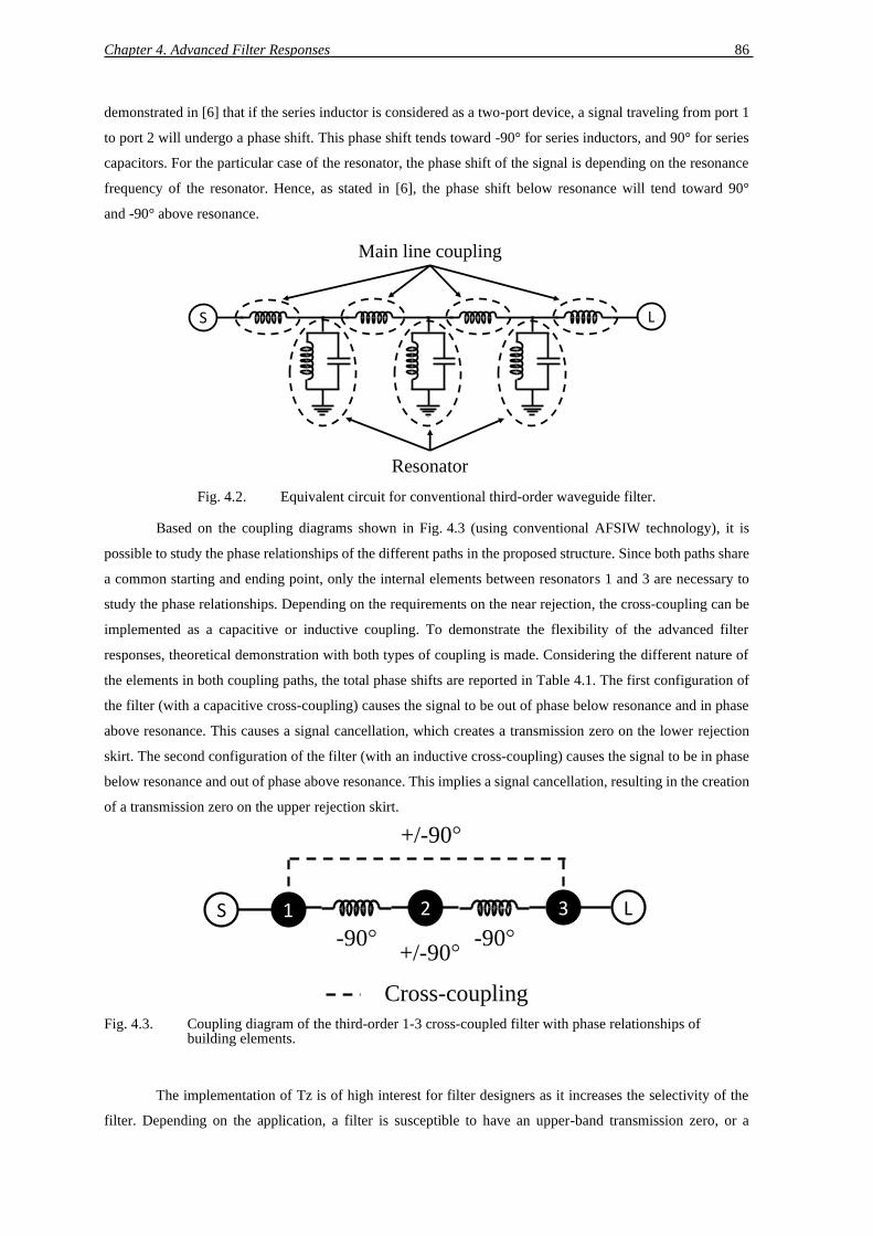
Chapter 4. Advanced Filter Responses 86
demonstrated in [6] that if the series inductor is considered as a two-port device, a signal traveling from port 1
to port 2 will undergo a phase shift. This phase shift tends toward -90° for series inductors, and 90° for series
capacitors. For the particular case of the resonator, the phase shift of the signal is depending on the resonance
frequency of the resonator. Hence, as stated in [6], the phase shift below resonance will tend toward 90°
and -90° above resonance.
Fig. 4.2. Equivalent circuit for conventional third-order waveguide filter.
Based on the coupling diagrams shown in Fig. 4.3 (using conventional AFSIW technology), it is
possible to study the phase relationships of the different paths in the proposed structure. Since both paths share
a common starting and ending point, only the internal elements between resonators 1 and 3 are necessary to
study the phase relationships. Depending on the requirements on the near rejection, the cross-coupling can be
implemented as a capacitive or inductive coupling. To demonstrate the flexibility of the advanced filter
responses, theoretical demonstration with both types of coupling is made. Considering the different nature of
the elements in both coupling paths, the total phase shifts are reported in Table 4.1. The first configuration of
the filter (with a capacitive cross-coupling) causes the signal to be out of phase below resonance and in phase
above resonance. This causes a signal cancellation, which creates a transmission zero on the lower rejection
skirt. The second configuration of the filter (with an inductive cross-coupling) causes the signal to be in phase
below resonance and out of phase above resonance. This implies a signal cancellation, resulting in the creation
of a transmission zero on the upper rejection skirt.
Fig. 4.3. Coupling diagram of the third-order 1-3 cross-coupled filter with phase relationships of building elements.
The implementation of Tz is of high interest for filter designers as it increases the selectivity of the
filter. Depending on the application, a filter is susceptible to have an upper-band transmission zero, or a
S L
Main line coupling
Resonator
S L1 2
-90
3
-90
Cross-coupling
+/-90
+/-90

Chapter 4. Advanced Filter Responses 87
lower-band transmission zero. To demonstrate the impact of Tz on the filter response, Fig. 4.4 represents the
selectivity (S21) of the three filters configuration previously discussed. It can be observed from Fig. 4.4 that the
implementation of a 1-3 inductive cross-coupling enables the filter to have a sharper near-band selectivity on
the upper-band of the filter compared to the conventional three poles. It can also be noticed that for this
particular topology, the selectivity on the lower-band of the filter is degraded compared to the conventional
three poles. For the implementation of a 1-3 capacitive cross-coupling, the opposite behavior can be observed.
Depending on the required specifications, the optimal filter configuration can be chosen.
TABLE 4.1
TOTAL PHASE SHIFTS OF THIRD ORDER CROSS-COUPLED AFSIW FILTER FOR BOTH PATHS WITH TWO
CROSS-COUPLING NATURES
Total phase shift Below resonance Above resonance
Path 1-2-3 -90°+90°-90° = -90° -90°-90°-90 = -270°
Path 1-3 (capacitive
coupling) +90° +90°
Result Out of phase (creation of Tz) In phase
Path 1-3 (inductive
coupling) -90° -90°
Result In phase Out of phase (creation of Tz)
Fig. 4.4. S21 parameters of the three filter topologies.
-4 -3 -2 -1 0 1 2 3 4-80
-60
-40
-20
0
Normalized frequency
|S21| (
dB
)
3 poles
3 poles with inductive cross-coupling
3 poles with capacitive cross-coupling

Chapter 4. Advanced Filter Responses 88
4. 1. 2. Cross-Coupling Implementation Using AFSIW
To implement a cross-coupling in AFSIW technology, it is possible to take advantage of the multilayer aspect
of the technology. A secondary path can be created using the top or bottom substrate. To do so, standard PCB
processes, such as etching, is used.
Fig. 4.5. 3D view of the third-order in-line arrow with 1-3 cross-coupling AFSIW filter.
Fig. 4.5 shows the proposed third-order in-line arrow configuration implementing a 1-3
cross-coupling filter. Path 1-2-3 is the primary path, located in substrate 2. The cross-coupling is implemented
in the bottom layer of the structure. To allow the signal propagation in the SIW transmission line, the top of
substrate 1 is etched with inductive iris, thus creating the secondary signal path (path 1-3). Considering this
type of cross-coupling, it is important to take into account the electrical length of the SIW transmission in the
total phase shift in addition to the nature of the cross-coupling. In this particular case, the coupling diagram
represented in Fig. 4.3 becomes the one shown in Fig. 4.6.
Fig. 4.6. Coupling diagram, with source/load coupling, of the third-order cross-coupled filter implemented in AFSIW technology using a SIW transmission line.
Copper Substrate Air
Substrate 3
Substrate 2
Substrate 1
zx
y
W
L
h1
h2
h3
Substrate 1 Substrate 2
S L1 2
-90
3
-90 +/-90
-90
ϕSIW

Chapter 4. Advanced Filter Responses 89
TABLE 4.2
TOTAL PHASE OF THIRD-ORDER 1-3 CROSS-COUPLED AFSIW FILTER SHIFTS FOR BOTH PATHS USING SIW
TRANSMISSION LINE
Total phase shift Below resonance Above resonance
Path 1-2-3 -90°+90°-90°= -90° -90°-90°-90° = -270°
Path 1-3 -90°+𝜙SIW -90°+𝜙SIW
Result with
𝜙SIW = 360° In phase Out of phase (creation of Tz)
Result with
𝜙SIW = 180° Out of phase (creation of Tz) In phase
As it is shown in Table 4.2, depending on the electrical length ϕSIW of the SIW transmission line, the
two presented types of coupling can be achieved. The electrical length ϕSIW must be chosen to be a multiple of
a half wavelength. It is of common knowledge that a half wavelength provides a 180° phase shift. Thus, by
playing with the additional phase shift created by the SIW transmission line, it is possible to have an equivalent
overall inductive cross-coupling (with ϕSIW = 360° or a multiple), thus creating a transmission zero on the
upper-band of the bandpass. On the other hand, if the electrical length of the SIW transmission is set to
ϕSIW = 180° or a multiple, the equivalent overall coupling is capacitive, hence creating a transmission zero on
the lower-band of the filter. The position of the transmission zero can be controlled by increasing or decreasing
the coupling between resonators 1 and 3 by changing the etched inductive coupling window dimensions.
4. 1. 3. Filter Design
In order to improve the near-band selectivity, the proposed principle is implemented on a third-order with 1-3
equivalent overall inductive cross-coupling. First, the filter is designed based on Chebyshev approximation
without the cross-coupling implementation. The proposed filter has been designed to operate at 21 GHz with
a fractional bandwidth of 1.43% (i.e., 300 MHz). Then the cross-coupling between resonators 1 and 3 is
implemented with a weak level using an SIW transmission line and an etched inductive iris. The correct phase
of the transmission line is obtained with W4 and L4 parameters. Finally, depending on the required
specifications, the coupling between resonators 1 and 3 is adjusted with the etched inductive iris. Few steps of
optimization are necessary to obtain the correct response for the cross-coupled filter design from the first filter
design. The filter is based on a multilayer PCB consisting of three Rogers RT/Duroid 6002 substrate with
thickness h1 = h3 = 0.508 mm and h2 = 1.524 mm. The geometric configuration of the structure is shown in
Fig. 4.7. All the dimensions are reported in Table 4.3.
(a)
Copper Substrate Air
W1 W2
L2
x2
W3
L3
L1
x1
L4
W4
x3x4
dx
dy
Metallized vias
Inductive iris
x5

Chapter 4. Advanced Filter Responses 90
(b)
Fig. 4.7. Top views of (a) substrate 1, implementing the secondary path with the cross-coupling, and (b) substrate 2 implementing the primary path with the three resonators.
TABLE 4.3
DIMENSIONS OF THE DESIGNED 1-3 CROSS-COUPLED AFSIW FILTER
Dimension i = 1 i = 2 i = 3 i = 4 i = 5
𝐿𝑖 (mm) 6 7.465 7.955 24.42 /
𝑥𝑖 (mm) 2 2 3.2 3 0.45
𝑊𝑖 (mm) 13 5.32 3.16 7 /
4. 1. 4. Robustness Against PCB Manufacturing Tolerances
In industry, a manufacturing process tolerance analysis is required to determine the yield of a filter topology.
For this reason, robustness against the standard PCB process milling tolerances (+/- 30 mils, approximately
+/- 0.0762 mm), the substrate permittivity uncertainty (+/- 0.04 considering Rogers RT/Duroid 6002) and the
standard multilayer PCB process substrate to substrate misalignment (+/- 30 mils, approximately
+/- 0.0762 mm), are evaluated. It should be noticed that more advanced PCB process class can be used to
provide lower tolerances, but at the expense of a higher cost.
A well-known approach to determine the sensitivity of a filter to dimensional random variations is to
perform a Monte Carlo analysis. For this purpose, the FEST3D simulator, using a +/- 0.0762 mm variation on
physical dimensions, has been used. Results are reported in Fig. 4.8(a). A variation of only +/- 1 MHz on the
rejection frequency location can be observed with a negligible impact on the center frequency and bandwidth.
Furthermore, the return loss remains above 15 dB.
As the cross-coupling of the proposed topology is made using an SIW transmission line in the bottom
substrate, a study of the substrate dielectric constant uncertainty is also needed. The datasheet of the particular
used substrate gives the uncertainty of the dielectric constant (+/ 0.04). Fig. 4.8(b), reporting S-parameters of
the filter obtained with the ANSYS HFSS simulator, shows that the variation of the dielectric constant has
almost no impact on the transmission zeros frequencies and other characteristics of the filter.
Finally, a study of the substrate to substrate misalignment is carried out. A suitable approach is to
evaluate the filter response to the worst cases of alignment using a full-wave simulator, here ANSYS HFSS.
In the proposed structure, the misalignment of substrate 1 and substrate 2 implies a misalignment of the etched
coupling windows. The results are shown in Fig. 4.8(c). It can be observed that with a worst case of 0.152 mm
misalignment in x and y directions, the frequency response is very slightly impacted.
The three studies highlight the high robustness of the proposed structure to PCB manufacturing
tolerances, and therefore its high interest for implementation.
Copper Substrate Air
W1 W2
L2
x2
W3
L3
L1
x1
L4
W4
x3x4
dx
dy
Metallized vias
Inductive iris
x5

Chapter 4. Advanced Filter Responses 91
(a)
(b)
(c) Fig. 4.8. Robustness analysis against (a) milling and drilling tolerances based on a Monte Carlo analysis
using FEST3D, (b) dielectric constant variation using HFSS and (c) multilayer misalignment using HFSS.
FEST3D
HFSS
HFSS
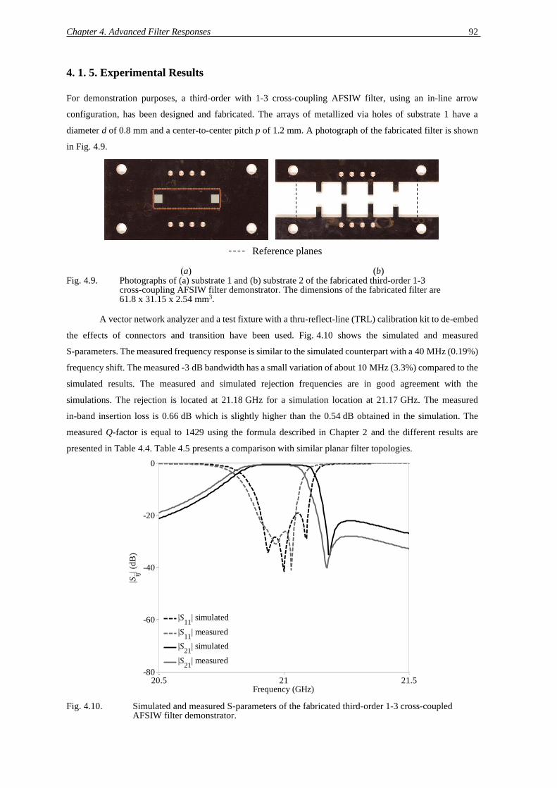
Chapter 4. Advanced Filter Responses 92
4. 1. 5. Experimental Results
For demonstration purposes, a third-order with 1-3 cross-coupling AFSIW filter, using an in-line arrow
configuration, has been designed and fabricated. The arrays of metallized via holes of substrate 1 have a
diameter d of 0.8 mm and a center-to-center pitch p of 1.2 mm. A photograph of the fabricated filter is shown
in Fig. 4.9.
(a) (b) Fig. 4.9. Photographs of (a) substrate 1 and (b) substrate 2 of the fabricated third-order 1-3
cross-coupling AFSIW filter demonstrator. The dimensions of the fabricated filter are 61.8 x 31.15 x 2.54 mm3.
A vector network analyzer and a test fixture with a thru-reflect-line (TRL) calibration kit to de-embed
the effects of connectors and transition have been used. Fig. 4.10 shows the simulated and measured
S-parameters. The measured frequency response is similar to the simulated counterpart with a 40 MHz (0.19%)
frequency shift. The measured -3 dB bandwidth has a small variation of about 10 MHz (3.3%) compared to the
simulated results. The measured and simulated rejection frequencies are in good agreement with the
simulations. The rejection is located at 21.18 GHz for a simulation location at 21.17 GHz. The measured
in-band insertion loss is 0.66 dB which is slightly higher than the 0.54 dB obtained in the simulation. The
measured Q-factor is equal to 1429 using the formula described in Chapter 2 and the different results are
presented in Table 4.4. Table 4.5 presents a comparison with similar planar filter topologies.
Fig. 4.10. Simulated and measured S-parameters of the fabricated third-order 1-3 cross-coupled AFSIW filter demonstrator.
Reference planes
20.5 21 21.5-80
-60
-40
-20
0
Frequency (GHz)
|Sij| (
dB
)
|S11
| simulated
|S11
| measured
|S21
| simulated
|S21
| measured

Chapter 4. Advanced Filter Responses 93
TABLE 4.4
COMPARISON OF SIMULATED AND MEASURED RESULTS OF THIRD-ORDER AFSIW CROSS-COUPLED FILTER
Characteristics Simulated (HFSS) Measured
Return loss (dB) > 22 > 22
Insertion loss (dB) 0.54 0.66
Center frequency (GHz) 21 20.96
Rejection frequency (GHz) 21.17 21.18
-3 dB bandwidth (MHz) 300 290
-3 dB bandwidth (%) 1.43 1.38
Unloaded Q-factor 1689 1429
TABLE 4.5
COMPARISON WITH SUBSTRATE INTEGRATED 1-3 CROSS-COUPLED FILTERS
Specifications [8] [9] [10] Proposed filter
Process PCB PCB PCB PCB
Technology Combline SIW SIW SIW AFSIW
PCB substrate material Rogers 4003 Rogers 5880 Rogers 6002 Rogers 6002
Filter order 3rd 3rd 4th 3rd
Total height (mm) 1.524 0.762 0.508 2.54
Area (mm²) 1880 561 121 1925
Center frequency (GHz) 5.3 13.35 35 20.96
-3 dB bandwidth (%) 4.9 8.99 8 1.38
Insertion loss (dB) 1.8 1.25 1.2 0.66
Rejection frequencies (GHz) 5.68 14.2 36.2 21.18
Unloaded Q-factor 147 115 180 1429
4. 2. Quasi-Elliptic Fourth-Order In-Line Configuration AFSIW
Filter
In this Section, based on the previous demonstration of an advanced filtering response using AFSIW
technology, a fourth-order quasi-elliptic AFSIW filter is presented. The filter configuration is a fourth-order
in-line arrow topology. In the proposed structure, a cross-coupling between non-adjacent resonators 1 and 4 is
implemented. The implementation of a 1-4 negative cross-coupling (in opposition to the sign of the coupling
between adjacent resonators) in a fourth-order filter allows the generation of two transmission zeros, above
and below the filter passband. This structure is of particular interest when the passband of the filter needs to be
highly isolated from other bands. A typical example is channel filters of a multiplexer.
4. 2. 1. Filter Topology
The proposed structure coupling diagram is represented in Fig. 4.11. The conventional fourth-order filter
allows only a single signal path (path 1-2-3-4), whereas the quasi-elliptic structure enables a secondary path
(path 1-4). The introduction of Tz can be explained by studying the phase relationships of the building blocks
of a bandpass filter as described in Section 4. 1.
The study on the phase relationships of the two paths is carried out. The coupling diagram of the
proposed structure using the AFSIW technology is represented in Fig. 4.12. The phase of the internal elements
to study is resonators 2 and 3 and also the couplings between resonators 1-2, 2-3, and 3-4.

Chapter 4. Advanced Filter Responses 94
(a) (b) Fig. 4.11. Coupling diagram of (a) the conventional fourth-order filter and (b) the fourth-order 1-4
cross-coupled filter, both with in-line arrow topologies.
The achievable responses of the proposed structure are studied depending on the nature of the
cross-coupling. The total phase shifts are reported in Table 4.6. The first configuration of the filter (with
inductive cross-coupling) causes the signal to be in phase both below and above resonance. This configuration
is of high interest to create imaginary transmission zeros to flatten the group delay. The second configuration
of the filter (with capacitive cross-coupling) allows the two signal paths to be out of phase below and above
the resonance. Hence, transmission zeros are created below and above the passband, substantially improving
the near-band selectivity of the filter.
Fig. 4.12. Coupling diagram of the fourth-order 1-4 cross-coupled filter with phase relationships of building elements.
TABLE 4.6
TOTAL PHASE SHIFTS OF QUASI-ELLIPTIC AFSIW FILTER FOR BOTH PATHS WITH TWO CROSS-COUPLING
NATURES
Total phase shift Below resonance Above resonance
Path 1-2-3-4 -90°+90°-90°+90°-90° = -90° -90°-90°-90 -90°-90°= -450°
Path 1-4 (capacitive
coupling) +90° +90°
Result Out of phase (creation of Tz) Out of phase (creation of Tz)
Path 1-4 (inductive
coupling) -90° -90°
Result In phase In phase
The quasi-elliptic structure allows implementing two transmission zeros below and above the
passband. At first glance, the generation of transmission zeros is of high interest for the selectivity of the filter.
Nevertheless, it can also be seen as a way to significantly reduce the size of the filter while maintaining the
same in- and near-band performances. To demonstrate this effect, Fig. 4.13 represents the selectivity (S21) of
conventional fourth-order, quasi-elliptic fourth-order, and sixth-order filters. It can be observed from Fig. 4.13
that the implementation of the 1-4 cross-coupling in the fourth-order filter allows the filter to have similar
selectivity levels in the near-band as a sixth-order filter, while maintaining the compactness of a fourth-order.
In other words, the same near-band electrical performances can be achieved while minimizing the volume of
the filter by 2 resonators and 2 coupling elements. It is also worthy to note that the implementation of the
S L1 2 3
Main line coupling
4 S L1 2 3 4
Main line coupling
Cross-coupling
S L1 2
-90
3
-90
Cross-coupling
+/-90
+/-90
4
-90 +/-90

Chapter 4. Advanced Filter Responses 95
quasi-elliptic fourth-order topology tends to lower the insertion loss of the filter compared to a conventional
fourth-order filter with the same specifications.
Fig. 4.13. S21 parameters of the conventional fourth- and sixth-order, and quasi-elliptic filter topologies.
4. 2. 2. Cross-Coupling Implementation Using AFSIW
Again, the proposed structure takes advantage of the AFSIW multilayer aspect. The cross-coupling is
implemented following the same idea as explained in Section 4. 1. The SIW transmission line is also
implemented in the bottom substrate of the structure to link two non-adjacent resonators.
Fig. 4.14. 3D view of quasi-elliptic fourth-order in-line arrow AFSIW filter.
-4 -3 -2 -1 0 1 2 3 4-80
-60
-40
-20
0
Normalized frequency
|S21| (
dB
)
4 poles
6 poles
4 poles quasi-elliptic
Copper Substrate Air
Substrate 3
Substrate 2
Substrate 1
zx
y
W
L
h1
h2
h3

Chapter 4. Advanced Filter Responses 96
Fig. 4.14 shows the proposed quasi-elliptic fourth-order in-line arrow AFSIW filter. The primary path
is generated by resonator 1-2-3-4. The secondary path is implemented using an SIW transmission line coupling
the non-adjacent resonators 1 and 4. The nature of the cross-coupling is given by property of the iris, which is
inductive in this particular implementation. Then, the electrical length ϕSIW is taken into account to obtain the
equivalent overall sign of the cross-coupling. The coupling diagram of the proposed structure taking into
account the electrical length of the transmission line is given in Fig. 4.15.
Fig. 4.15. Coupling diagram of the quasi-elliptic fourth-order filter implemented in AFSIW technology using a SIW transmission line.
TABLE 4.7
TOTAL PHASE SHIFTS OF QUASI-ELLIPTIC AFSIW FILTER FOR BOTH PATHS USING SIW TRANSMISSION LINE
Total phase shift Below resonance Above resonance
Path 1-2-3 -90°+90°-90°+90°-90° = -90°° -90°-90°-90 -90°-90°= -450°
Path 1-4 -90°+𝜙SIW -90°+𝜙SIW
Result with
𝜙SIW = 360° In phase In phase
Result with
𝜙SIW = 180° Out of phase (creation of Tz) Out of phase (creation of Tz)
The Table 4.7 shows the total phase shifts of the two paths with different equivalent overall
cross-coupling natures. It is stated that if the electrical length ϕSIW of the SIW transmission line is equal to 360°
or a multiple, the two paths are in phase, hence creating imaginary transmission zeros below and above the
resonance, allowing flattening the group delay. On the other hand, if the electrical length ϕSIW of the SIW
transmission line is equal to 180° or a multiple, a signal cancellation occurs and creates a transmission zero on
the lower (below resonance) and upper (above resonance) skirt. This is due to the equivalent overall coupling
being capacitive. The transmission zeros positions can be controlled by increasing or decreasing the coupling
by adjusting the coupling window.
4. 2. 3. Filter Design
To demonstrate the proposed quasi-elliptic principle, an equivalent overall capacitive 1-4 cross-coupling is
implemented on a conventional fourth-order AFSIW filter. Using a Chebyshev approximation, it is possible to
synthesize the fourth-order AFSIW filter without the cross-coupling. The proposed filter has been designed to
have a central frequency of 21 GHz with a fractional bandwidth of 1.67% (i.e., 350 MHz). Following, the
implementation of the 1-4 cross-coupling is made with a weak level. The correct phase of the SIW transmission
line is controlled by the physical dimensions W5 and L4. Depending on the required specifications, the coupling
level is increased while maintaining the resonance frequencies of the resonators. Few steps of optimization are
necessary to obtain the correct response for the cross-coupled filter design from the first filter design. The filter
S L1 2
-90
3
-90 +/-90
-90
4
-90 +/-90
Substrate 1 Substrate 2
ϕSIW

Chapter 4. Advanced Filter Responses 97
is based on the same process as presented in Sections 4. 1 and 4. 2 with the same materials and thickness. All
the dimensions of the designed filter are given in Table 4.8. The geometric implementation of the filter is given
in Fig. 4.16.
(a)
(b) Fig. 4.16. Top views of (a) substrate 1, implementing the secondary path with the 1-4 cross-coupling, and
(b) substrate 2 implementing the primary path with the four resonators.
TABLE 4.8
DIMENSIONS OF THE DESIGNED QUASI-ELLIPTIC AFSIW FILTER
Dimension i = 1 i = 2 i = 3 i = 4 i = 5 i = 6
𝐿𝑖 (mm) 6 7.226 7.964 28.154 / /
𝑥𝑖 (mm) 2 2 2 0.8 2.75 0.3
𝑊𝑖 (mm) 13 5.356 3.334 3.161 7 /
4. 2. 4. Robustness Against PCB Manufacturing Tolerances
For the same reasons as explained in Section 4. 1. 4, robustness against the PCB process milling tolerances
(+/- 0.0762 mm), the substrate permittivity uncertainty (+/- 0.04 considering Rogers RT/Duroid 6002) and the
standard multilayer PCB process substrate to substrate misalignment (+/- 0.0762 mm), are evaluated.
The results of the Monte Carlo analysis using the FEST3D simulator with a +/- 0.0762 mm variation
on physical dimensions is shown in Fig. 4.17(a). A variation of +/- 2 MHz on the rejection frequencies
locations is observed. It has a negligible impact on the center frequency and the bandwidth of the structure.
The study of the substrate dielectric constant uncertainty is carried out. The same datasheet given by
Rogers is used to obtain the dielectric constant uncertainty. Then, using a full-wave simulator, here ANSYS
HFSS, the impact of this uncertainty is studied on the proposed structure. Fig. 4.17(b) reports S-parameters of
the filter with a variation of +/- 0.04 of the dielectric constant of the SIW transmission line. It can be observed
that it has no impact on the location of the transmission zeros.
Copper Substrate Air
W1 W2
L2
x2
W3
L3
L1
x1
L4
W5
x4 x5
dx
dy
Metallized vias
Inductive iris
x6
W4
x3
Copper Substrate Air
W1 W2
L2
x2
W3
L3
L1
x1
L4
W5
x4 x5
dx
dy
Metallized vias
Inductive iris
x6
W4
x3

Chapter 4. Advanced Filter Responses 98
(a)
(b)
(c) Fig. 4.17. Robustness analysis against (a) milling and drilling tolerances based on a Monte Carlo analysis
using FEST3D, (b) dielectric constant variation using HFSS and (c) multilayer misalignment using HFSS.
FEST3D
HFSS
HFSS

Chapter 4. Advanced Filter Responses 99
The last study concerns the substrate to substrate misalignment. The same approach as in Section 4. 1
is used. The misalignment of substrates 1 and 2 is studied using the full-wave ANSYS HFSS simulator. The
results are shown in Fig. 4.17(c). It can be observed that with a worst case of 0.152 mm misalignment in x and
y directions, the frequency response is very slightly impacted.
The three studies show the high robustness of the proposed structure to PCB manufacturing tolerances,
substrate dielectric constant uncertainty, and substrate to substrate misalignment.
4. 2. 5. Experimental Results
For demonstration purpose, a quasi-elliptic fourth-order with 1-4 cross-coupling AFSIW filter, using an in-line
arrow configuration, has been designed and fabricated. The arrays of metallized via holes have the same
dimensions as detailed previously. A photograph of the fabricated filter is given in Fig. 4.18.
(a) (b) Fig. 4.18 Photographs of (a) substrate 1 and (b) substrate 2 of the fabricated quasi-elliptic fourth-order
AFSIW filter demonstrator. The dimensions of the fabricated filter are 71.4 x 31.15 x 2.54 mm3.
The measurement of the fabricated prototype has been achieved using the same flow (vector network
analyzer, test fixture, and TRL calibration kit). The comparison between simulated and measured results is
given in Fig. 4.19. The measured center frequency is 20.99 GHz compared to 21 GHz in simulations. The
measured bandwidth of the filter is 280 MHz, slightly smaller than the 300 MHz of the simulated results. The
measured rejection frequencies are located at 20.77 GHz and 21.22 GHz. The return loss of the measured filter
remains greater than 20 dB. Finally, the measured in-band insertion loss is 0.78 dB. The obtained Q-factor of
the measured filter is evaluated to 1613. All the measured results are presented in Table 4.9.
TABLE 4.9
COMPARISON OF SIMULATED AND MEASURED RESULTS OF QUASI-ELLIPTIC AFSIW
Characteristics Simulated (HFSS) Measured
Return loss (dB) > 22 > 22
Insertion loss (dB) 0.7 0.78
Center frequency (GHz) 21 20.99
Rejection frequencies (lower/upper) (GHz) 20.72 / 21.24 20.77 / 21.22
-3 dB bandwidth (MHz) 300 280
-3 dB bandwidth (%) 1.43 1.34
Unloaded Q-factor 1737 1613
Reference planes

Chapter 4. Advanced Filter Responses 100
Fig. 4.19. Simulated and measured S-parameters of the fabricated quasi-elliptic AFSIW filter demonstrator.
4. 2. 6. Drawbacks of the In-Line Configuration
As previously explained, the implemented cross-coupling is not purely inductive or capacitive. Indeed, the total
phase contribution consists of the nature of the cross-coupling plus the SIW transmission line electrical length.
This will cause the signal to be periodically out of phase or in phase depending on the frequency. This causes
periodical resonance peak all along the propagation frequency range.
Those spurious resonances degrade the wideband response of the filter. Fig. 4.20 represents the
wideband response of the two fabricated prototypes. It can be observed that spurious resonances are located
below and above the passband, preventing the filter to have a high-wideband isolation. The frequency shift of
the resonance peaks is due to a fabrication process error. The inductive iris allowing the implementation of the
secondary path was etched on the top and bottom copper layers of substrate 1, instead of only the top copper
layer. Thus, an electromagnetic shield was implemented manually to prevent the signal from leaking.
20.5 21 21.5-80
-60
-40
-20
0
Frequency (GHz)
|Sij| (
dB
)
|S11
| simulated
|S11
| measured
|S21
| simulated
|S21
| measured

Chapter 4. Advanced Filter Responses 101
(a) (b) Fig. 4.20. Simulated and measured S-parameters of (a) the third-order 1-3 cross-coupled and (b) the
fourth-order 1-4 cross-coupled in-line configuration filters.
4. 3. Quasi-Elliptic Fourth-Order Folded Configuration AFSIW
Filter
In this Section, taking into consideration the different drawbacks of the in-line arrow configuration, a
quasi-elliptic fourth-order filter with a folded configuration is presented. The folded configuration allows
minimizing the electrical length of the cross-coupling, hence minimizing the periodicity of its resonance.
4. 3. 1. Filter Topology
The coupling diagram of the folded structure is shown in Fig. 4.21(a). The coupling diagram using the AFSIW
technology is given in Fig. 4.21(b). The study on the phase relationships is the same as the one presented in
Section 4. 2 (i.e., primary path 1-2-3-4 and secondary path 1-4).
(a) (b) Fig. 4.21. Coupling diagram of (a) the conventional fourth-order filter and (b) the fourth-order 1-4
cross-coupled filter, both with folded topologies.
4. 3. 2. Cross-Coupling Implementation Using AFSIW
Similarly, to the previous Sections, the cross-coupling between the non-adjacent resonators 1 and 4 is
implemented using the bottom substrate of the multilayer structure. The 3D view of the proposed structure is
shown in Fig. 4.22.
S L1
2
4
3
-90 -90
-90 +/-90 +/-90
+/-90
S L1
2
4
3
Main line coupling
Cross-coupling

Chapter 4. Advanced Filter Responses 102
Fig. 4.22. 3D view of quasi-elliptic fourth-order folded AFSIW filter.
Fig. 4.23 shows the proposed quasi-elliptic fourth-order folded AFSIW filter coupling diagram
implementation. The primary path is generated by resonator 1-2-3-4. The secondary path is implemented using
a SIW transmission line coupling non-adjacent resonators 1 and 4. The folded configuration of the filter allows
minimizing the length and thus electrical length of the SIW transmission line. Indeed, the folded configuration
enables resonators 1 and 4 to be closer (1 coupling) than the in-line arrow configuration (3 couplings and 2
resonators).
Fig. 4.23. Coupling diagram of the quasi-elliptic fourth-order filter implemented in AFSIW technology using a SIW transmission line.
TABLE 4.10
TOTAL PHASE SHIFTS OF QUASI-ELLIPTIC FOLDED AFSIW FILTER FOR BOTH PATHS USING SIW
TRANSMISSION LINE
Total phase shift Below resonance Above resonance
Path 1-2-3 -90°+90°-90°+90°-90° = -90°° -90°-90°-90 -90°-90°= -450°
Path 1-4 -90°+𝜙SIW -90°+𝜙SIW
Result with
𝜙SIW = 360° In phase In phase
Result with
𝜙SIW = 180° Out of phase (creation of Tz) Out of phase (creation of Tz)
Table 4.10 shows that to obtain a quasi-elliptic function, it is necessary to implement a SIW
transmission line with an electrical length ϕSIW equal to 180°. Hence, the equivalent overall nature of the
cross-coupling is capacitive and transmission zeros below and above the passband of the filter are created.
Copper Substrate Air
Substrate 3
Substrate 2
Substrate 1
zx
yW
L
h1
h2
h3
S L1
2
4
3
ϕSIW
-90 -90
-90
-90
+/-90 +/-90
Substrate 1 Substrate 2

Chapter 4. Advanced Filter Responses 103
4. 3. 3. Filter Design
To demonstrate the proposed quasi-elliptic folded principle, a filter with the same specifications as the one
presented in Section 4. 2 is designed. The geometry of the filter is shown in Fig. 4.24. The correct phase of the
SIW transmission line is controlled by the physical dimensions W6 and L5. The position of the transmission
zeros can be controlled by playing with the inductive coupling between resonators 1 and 4. The dimensions of
the designed filter are given in Table 4.11.
(a)
(b) Fig. 4.24. Top views of (a) substrate 1, implementing the secondary path with the 1-4 cross-coupling, and
(b) substrate 2 implementing the primary path of the quasi-elliptic folded filter.
TABLE 4.11
DIMENSIONS OF THE DESIGNED QUASI-ELLIPTIC FOLDED AFSIW FILTER
Dimension i = 1 i = 2 i = 3 i = 4 i = 5 i = 6
𝐿𝑖 (mm) 6 8.042 9.202 6.9 / /
𝑥𝑖 (mm) 2 2 2 1.7 2.2 /
𝑊𝑖 (mm) 13 5.547 10.16 3.684 10.16 3.33
4. 3. 4. Robustness Against PCB Manufacturing Tolerances
Studies similar to the ones described in Section 4. 1 are carried out to determine the yield of the proposed
structure. The same conclusions concerning the PCB manufacturing tolerances, substrate dielectric constant
uncertainty, and substrate to substrate misalignment can be made. Those studies prove the high interest of the
proposed structure to implement high performance, compact, and high selectivity AFSIW filters.
W7
x3
dx
dy
Metallized vias
Inductive iris
x5
L4
x4
Copper Substrate Air
W1W2
L1
x1
W3
L2
W4
W5
L3
W6
x2
x3

Chapter 4. Advanced Filter Responses 104
(a)
(b)
(c) Fig. 4.25. Robustness analysis against (a) milling and drilling tolerances based on a Monte Carlo analysis
using FEST3D, (b) dielectric constant variation using HFSS and (c) multilayer misalignment using HFSS.
FEST3D
HFSS
HFSS

Chapter 4. Advanced Filter Responses 105
4. 3. 5. Experimental Results
For demonstration purpose, a quasi-elliptic fourth-order with 1-4 cross-coupling AFSIW filter, using folded
configuration, has been designed and fabricated. The arrays of metallized via have the same dimensions as the
ones detailed previously. A photograph of the fabricated filter is shown in Fig. 4.26.
(a) (b) Fig. 4.26. Photographs of (a) substrate 1 and (b) substrate 2 of the fabricated quasi-elliptic fourth-order
folded AFSIW filter demonstrator. The dimensions of the fabricated filter are 54.2 x 37.3 x 2.54 mm3.
The measurement flow is the same as the one described in Section 4. 1. Comparison between
simulation and measurement is shown in Fig. 4.27. The measured centre frequency is 20.9 GHz. The
measured -3 dB bandwidth of the filter is 360 MHz, presenting an increase of 10 MHz compared to the
simulation. The transmission zeros frequencies are located at 20.63 GHz and 21.25 GHz, very similar to the
simulated locations. The return loss of the filter remains greater than 18 dB in the passband. The measured
in-band insertion loss is 0.7 dB, similar to the 0.6 dB obtained in simulations with a measured Q-factor of 1478.
As it is demonstrated in Fig. 4.28, the wideband response of the filter is clean of spurious peaks until 23 GHz.
A comparison between simulated and measured results is given in Table 4.12. A comparison to quasi-elliptic
filters based on planar technologies is given in Table 4.13.
TABLE 4.12
COMPARISON OF SIMULATED AND MEASURED RESULTS OF THE QUASI-ELLIPTIC FOLDED AFSIW FILTER
Characteristics Simulated (HFSS) Measured
Return loss (dB) > 22 > 21
Insertion loss (dB) 0.6 0.7
Center frequency (GHz) 20.9 20.89
Rejection frequencies (lower/upper) (GHz) 20.64 / 21.25 20.63 / 21.25
-3 dB bandwidth (MHz) 350 360
-3 dB bandwidth (%) 1.66 1.71
Unloaded Q-factor 1745 1478
Reference planes

Chapter 4. Advanced Filter Responses 106
Fig. 4.27. In-band simulated and measured S-parameters of the fabricated quasi-elliptic folded AFSIW filter demonstrator.
Fig. 4.28. Wideband simulated and measured S-parameters of the fabricated quasi-elliptic folded AFSIW filter demonstrator.
20.5 21 21.5-80
-60
-40
-20
0
Frequency (GHz)
|Sij| (
dB
)
|S11
| simulated
|S11
| measured
|S21
| simulated
|S21
| measured
19 20 21 22 23-80
-60
-40
-20
0
Frequency (GHz)
|Sij| (
dB
)
|S11
| simulated
|S11
| measured
|S21
| simulated
|S21
| measured

Chapter 4. Advanced Filter Responses 107
TABLE 4.13
COMPARISON WITH SUBSTRATE INTEGRATED QUASI-ELLIPTIC FILTERS
Specifications [11] [12] [13] Proposed filter
Process PCB PCB PCB PCB
Technology Combline SIW SIW SIW AFSIW
PCB substrate material Rogers TMM4 Rogers 5880 Taconic TLY-5 Rogers 6002
Filter order 4th 4th 4th 4th
Total height (mm) 3.175 0.508 0.508 2.54
Area (mm²) 450 350 100 1560
Center frequency (GHz) 5.68 20.5 27 20.99
-3 dB bandwidth (%) 1.8 3.41 7.41 1.71
Insertion loss (dB) 3.6 0.9 2.1 0.71
Rejection frequencies (GHz) 5.56 / 5.8 19.6 / 21.4 25.6 / 28.4 20.63 / 21.25
Unloaded Q-factor 225 520 116 1478
4. 4. Higher Order Filter
In order to extend the principle of cross-couplings, a potential implementation, benefiting from the high
Q-factor, compactness, and self-packaging characteristic of AFSIW, is studied. The application requires a set
of realistic specifications, leading to the design of a seventh-order AFSIW bandpass filter operating in the
satcom uplink Ku-band. The filter implements the proposed cross-coupling principle.
4. 4. 1. Filter Specifications
In most of the emerging telecommunication applications, highly compact and easily integrated microwave filter
is highly desired. The foreseen application, using the cross-coupling principle, is the implementation of an
IMUX operating in the Ku-band. The cross-coupling allows the introduction of transmission zeros below and
above the passband of a filter which greatly increases the isolation of the different channels. It also allows the
reduction of the guard bands, hence leading to an optimized utilization of the frequency spectrum. For the
implementation of an IMUX, the channel filters must have very strong near rejection, flat insertion loss and
group delay responses, high Q-factor, be compact and self-packaged.
Therefore, a specification of a channel filter operating in the Ku-band is studied. The filter
requirements are very stringent on the near rejection and insertion loss variation. It is highly desired to minimize
the insertion loss. Finally, the filter must be compact compared to the presently used technologies.
The frequency mask of the channel filter of the Ku-band is given in Fig. 4.29. A detailed list of the
required specifications is given in Table 4.14.

Chapter 4. Advanced Filter Responses 108
Fig. 4.29. Frequency mask of the Ku-band filter.
TABLE 4.14
SPECIFICATION OF THE REQUIRED KU-BAND FILTER
Specification
Return loss (dB) > 20
Insertion loss (dB) < 3
Center frequency (GHz) 12.05
Near rejection
f0 ± 144 MHz
f0 ± 380 MHz
f0 ± 430 MHz
20 dB
40 dB
40 dB
Insertion loss variation
f0 ± 60 MHz
f0 ± 100 MHz
f0 ± 118 MHz
0.3 dBpp
0.5 dBpp
1.1 dBpp
Group delay variation
f0 ± 60 MHz
f0 ± 100 MHz
f0 ± 118 MHz
3 nspp
6 nspp
20 nspp
-3 dB bandwidth (MHz) 260
4. 4. 2. Filter Design
In order to be compliant with the near-rejection specifications and size limitations, the proposed solution for
satisfying the requirements is a seventh-order filter with two transmission zeros located below and above the
passband. This solution is a trade-off between size and performance to ensure a good rejection level with low
insertion loss. To achieve the transmission zeros, the proposed principle detailed in the previous Section is
used. Taking into considerations the previous Sections, the filter topology is implemented in an in-line folded
configuration in order to minimize the length of the SIW transmission lines. The filter topology is given in
Fig. 4.30. The filter is designed, without the cross-couplings, to operate at 12.05 GHz with a -3 dB bandwidth
equal to 260 MHz (2.16%). Then the cross-couplings between resonators 1 and 4, and resonators 3 and 6, are
implemented with a weak level using a SIW transmission line and an etched inductive iris as described in
previous Sections. The correct phase of the transmission line is obtained with the width and length of the
11.05 11.55 12.05 12.55 13.05-80
-60
-40
-20
0
Frequency (GHz)
Lev
el (
dB
)

Chapter 4. Advanced Filter Responses 109
transmission line. Finally, depending on the required specifications, the coupling between resonators 1 and 4,
and resonators 3 and 6 is adjusted with the etched inductive iris. The filter is based on a multilayer PCB
consisting of two Rogers RT/Duroid 6002 substrate with thickness h1 = h3 = 0.508 mm and a Rogers
RT/Duroid 6010 with h2 = 1.905 mm. The geometric configuration of the structure is shown in Fig. 4.31. All
the dimensions are reported in Table 4.15. The group delay variation specifications are not too severe and thus
do not need to be flattened using imaginary transmission zeros.
Fig. 4.30. Coupling diagram of the quasi-elliptic seventh-order filter implemented in AFSIW technology using two SIW transmission lines.
The quasi-elliptic response is implemented using two cross-couplings, between resonators 1 and 4,
and resonators 3 and 6 as illustrated in Fig. 4.31. The minimal path rule allows the seventh-order filter to
implement a maximum of 2 transmission zeros. It is worthy to note that two cross-couplings were implemented
in our case, but it is also possible to introduce a single cross-coupling (with a stronger coupling) to achieve the
same response. The transmission zeros can be controlled, with the etched coupling window, to achieve the
desired near rejection levels and thus reach the desired near rejection level.
(a)
S 1
2
4
3
5
6 L7
ϕSIW
ϕSIW
-90
+/-90 -90
-90 -90
-90 -90
+/-90
+/-90 +/-90
-90
Substrate 1 Substrate 2
-90 +/-90
W13
x12
dx
dy
Metallized vias
Inductive iris
x14
L11
x13
W12
x9
x11
L10
x10

Chapter 4. Advanced Filter Responses 110
(b)
Fig. 4.31. Top views of (a) substrate 1, implementing the secondary path with the 1-4 and 3-6 cross-couplings, and (b) substrate 2 implementing the primary path of the quasi-elliptic folded filter.
TABLE 4.15
DIMENSIONS OF THE DESIGNED KU-BAND SEVENTH-ORDER AFSIW FILTER
Dimension i = 1 i = 2 i = 3 i = 4 i = 5 i = 6 i = 7 i = 8 i = 9 i = 10 i = 11 i = 12 i = 13 i = 14
𝐿𝑖 (mm) 10 13.985 14.838 15.496 15.486 14.921 14.726 13.39 10 15.953 15.953 / / /
𝑥𝑖 (mm) 2 2 2 2 2 2 2 2 1.5 3.813 1.02 1.5 3.813 1.02
𝑊𝑖 (mm) 19.05 8.898 5.469 20.3 5.652 5.177 5.51 5.51 7.103 9.782 19.05 9.82 9.82 5.652
4. 4. 3. Experimental Results
For demonstration purpose, a quasi-elliptic seventh-order with 1-4 and 3-6 cross-couplings AFSIW filter, using
an in-line folded configuration, has been designed and fabricated. The arrays of metallized via have the same
dimensions as in previous Sections. A photograph of the fabricated filter is given in Fig. 4.32.
(a) (b)
Fig. 4.32. Photographs of (a) substrate 2 and (b) substrate 1 of the fabricated Ku-band AFSIW filter. The
dimensions of the fabricated filter are 107.3 x 52.4 x 5.95 mm3.
A vector network analyzer and a test fixture with a thru-reflect-line (TRL), operating at the Ku-band,
calibration kit to de-embed the effects of connectors and transition have been used. The simulated and measured
S-parameters are shown in Fig. 4.33. It can be observed that the response has a frequency shift equal to 48 MHz
(0.4%). The measured -3 dB bandwidth is 253 MHz similar to the 260 MHz in the simulation. The measured
rejection levels are in good agreement with the simulations but the frequency shift. The measured in-band
Copper Substrate Air
W1W2
L1
x3
L2
W3
W4
L3
W5
x4
x5
W6
L4
L5 L6
L7
W7
W9 W10
W8
L8
W11
L9x6x2
x1
x7
x8
Reference planes

Chapter 4. Advanced Filter Responses 111
insertion loss is 0.78 dB which is slightly higher than the 0.76 dB obtained in the simulation. The measured
Q-factor is equal to 1945. The measured results are given in Table 4.16.
Fig. 4.33. Simulated and measured S-parameters of the fabricated seventh-order AFSIW filter demonstrator.
TABLE 4.16
COMPARISON OF SIMULATED AND MEASURED RESULTS OF KU-BAND SEVENTH-ORDER QUASI-ELLIPTIC
FOLDED AFSIW FILTER
Characteristics Simulated (HFSS) Measured
Return loss (dB) > 22 > 20
Insertion loss (dB) 0.72 0.76
Center frequency (GHz) 12.05 12.0
Rejection frequencies (lower/upper) (GHz) 11.9 / 12.21 11.85 / 12.16
-3 dB bandwidth (MHz) 260 253
-3 dB bandwidth (%) 2.16 2.1
Unloaded Q-factor 1957 1945
For comparison purposes, the measured results of the seventh-order filter were shifted in frequency to
be able to compare the measured results with the required specifications. Thus, Fig. 4.34 shows the measured
results of the filter shifted by 50 MHz. The rejection mask is represented in Fig. 4.34. It can be observed that
the filter is compliant with the required near rejection specifications. The measured return loss remains greater
than 20 dB, which was also a required specification. The measured insertion loss is 0.78 dB, which is compliant
with the required 3 dB.
For the insertion loss variation, the first required specification of 0.3 dBpp (peak to peak) ± 60 MHz
from the central frequency is compliant, so is the second and third specification of 0.5 dBpp ± 100 MHz, and
11.6 11.8 12 12.2 12.4-80
-60
-40
-20
0
Frequency (GHz)
|Sij| (
dB
)
|S11
| simulated
|S11
| measured
|S21
| simulated
|S21
| measured

Chapter 4. Advanced Filter Responses 112
1.1 dBpp ± 118 MHz from f0. The measured results are compared to the simulations and specifications mask
in Fig. 4.35.
Concerning the group delay variation, Fig. 4.36 shows the comparison between simulation and
measurement of the group delay. The three specifications of 3 ns ± 60 MHz, 6 ns ± 100 MHz, and 20 ns
± 118 MHz are fulfilled.
The required specifications are listed in Table 4.17. The status of the filter (compliant or not
compliant) is also listed in this table. It is demonstrated in this Section that all the required electrical
specifications have been fulfilled for a high order filter using the proposed cross-coupling principle.
Fig. 4.34. Measured S-parameters, with the applied frequency shift (50 MHz), of the fabricated seventh-order AFSIW filter demonstrator with the specifications mask.
11.65 11.85 12.05 12.25 12.45-80
-60
-40
-20
0
Frequency (GHz)
|Sij| (
dB
)
|S11
| measured with frequency shift
|S21
| measured with frequency shift

Chapter 4. Advanced Filter Responses 113
Fig. 4.35. Simulated and measured insertion loss variation, with the applied frequency shift (50 MHz), of the fabricated seventh-order AFSIW filter demonstrator with the specifications mask.
Fig. 4.36. Simulated and measured group delay variation, with the applied frequency shift (50 MHz), of the fabricated seventh-order AFSIW filter demonstrator with the specifications mask.
11.85 11.95 12.05 12.15 12.25-3
-2.5
-2
-1.5
-1
-0.5
0
Frequency (GHz)
|S21| (
dB
)
|S21
| simulated
|S21
| measured
11.85 11.95 12.05 12.15 12.250
5
10
15
20
25
30
Frequency (GHz)
Gro
up
del
ay (
ns)
Group delay simulated
Group delay measured
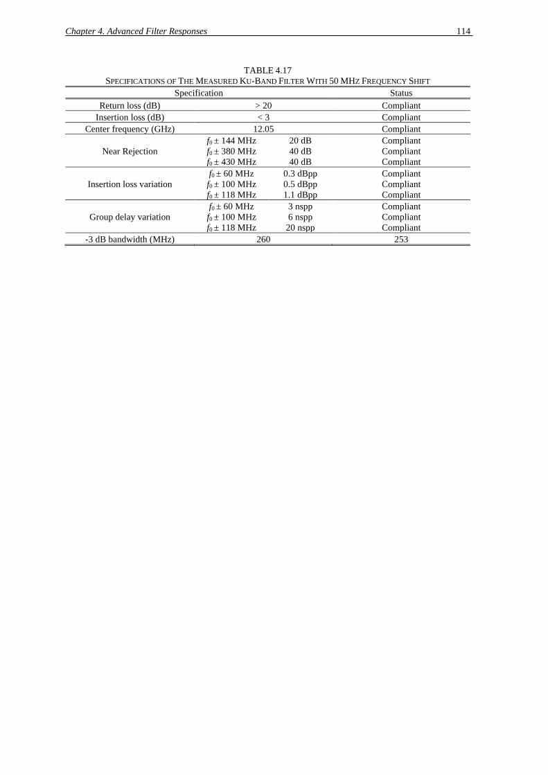
Chapter 4. Advanced Filter Responses 114
TABLE 4.17
SPECIFICATIONS OF THE MEASURED KU-BAND FILTER WITH 50 MHZ FREQUENCY SHIFT
Specification Status
Return loss (dB) > 20 Compliant
Insertion loss (dB) < 3 Compliant
Center frequency (GHz) 12.05 Compliant
Near Rejection
f0 ± 144 MHz
f0 ± 380 MHz
f0 ± 430 MHz
20 dB
40 dB
40 dB
Compliant
Compliant
Compliant
Insertion loss variation
f0 ± 60 MHz
f0 ± 100 MHz
f0 ± 118 MHz
0.3 dBpp
0.5 dBpp
1.1 dBpp
Compliant
Compliant
Compliant
Group delay variation
f0 ± 60 MHz
f0 ± 100 MHz
f0 ± 118 MHz
3 nspp
6 nspp
20 nspp
Compliant
Compliant
Compliant
-3 dB bandwidth (MHz) 260 253

Chapter 4. Advanced Filter Responses 115
4. 5. Conclusions
In this Chapter, a novel technique to introduce transmission zeros in filters based on AFSIW technology is
theoretically studied and demonstrated from simulations and measurements. The proposed technique takes
advantage of the multilayer aspect of the technology to implement a secondary path into the bottom substrate.
By playing with the phase of the different paths, a signal cancellation creating a transmission zero can be
created. The proposed technique can be implemented in conventional filter configurations (in-line arrow,
folded, in-line folded…). For demonstration purposes, the principle was implemented in the Ka-band on a
third- and fourth-order in-line arrow configuration, and fourth-order folded configuration. The fabricated filters
present good results compared to simulations. To further extend the work, the proposed principle was
implemented on a higher order filter. The design was faced to real specifications for operation in the satcom
uplink Ku-band. Hence, a seventh-order AFSIW filter with a double cross-coupling was fabricated. The filter
shows very good results and is compliant with almost the full list of specifications. The proposed principle is
foreseen to be implemented in an IMUX operating in the Ku-band. The transmission zeros allow a reduction
of the guard band and increase the compactness of the device. To be able to operate in space conditions, it is
necessary to study the impact of the external environment on the filter response. This problematic will be
studied in the next Chapter.

Chapter 4. Advanced Filter Responses 116
References
[1] T. Martin, A. Ghiotto, T.P. Vuong, F. Lotz, and P. Monteil, “High performance air-filled substrate
integrated waveguide filter post-process tuning using capacitive post,” IEEE MTT-S Int. Microw.
Symp., Hawaii, HI, Jun. 2017, pp. 196-199.
[2] T. Martin, A. Ghiotto, F. Lotz, and T.P. Vuong, “Fabrication-tolerant reconfigurable AFSIW filters
based on through-hole mounted metallic posts for versatile high performance systems,” IEEE MTT-S
Int. Microw. Symp., Philadelphia, PA, Jun. 2018, pp. 319-322.
[3] T. Martin, A. Ghiotto, T.P. Vuong, and F. Lotz, “Fabrication-tolerant AFSIW filters based on
quadruplet through-hole mounted inductive posts,” Eur. Microw. Conf. (EuMC), Madrid, 2018.
[4] T. Martin, A. Ghiotto, T.P. Vuong, and F. Lotz, “Configurable perforated air-filled substrate
integrated waveguide (AFSIW) for generic high-performance systems on substrate,” IEEE
Transactions on Microwave Theory and Techniques, to be published.
[5] R. M. Kurzrok, “General three-resonator filters in waveguide,” IEEE Transactions on Microwave
Theory and Techniques, vol. 14, no. 1, pp. 46-47, Jan. 1966.
[6] J. B. Thomas, “Cross-coupling in coaxial cavity filters - a tutorial overview,” IEEE Transactions on
Microwave Theory and Techniques, vol. 51, no. 4, pp. 1368-1376, Apr. 2003.
[7] R. Levy, “Filters with single transmission zeros at real or imaginary frequencies,” IEEE
Transactions on Microwave Theory and Techniques, vol. 24, no. 4, pp. 172-181, Apr. 1976.
[8] J. D. Martínez, S. Sirci and V. E. Boria, “Compact SIW filter with asymmetric frequency response
for C-band wireless applications,” IEEE International Wireless Symposium (IWS), Beijing, 2013,
pp. 1-4.
[9] S. Deng, F. Xu and L. Yang, “A compact bandpass filter with transmission zero based on SIW
triangular cavities,” IEEE International Conference on Ubiquitous Wireless Broadband (ICUWB),
Nanjing, 2016, pp. 1-3.
[10] X. Chen and K. Wu, “Self-packaged millimeter-wave substrate integrated waveguide filter with
asymmetric frequency response,” IEEE Transactions on Components, Packaging and
Manufacturing Technology, vol. 2, no. 5, pp. 775-782, May 2012.
[11] S. Sirci, F. Gentili, J. D. Martínez, V. E. Boria, and R. Sorrentino, “Quasi-elliptic filter based on
SIW combline resonators using a coplanar line cross-coupling,” IEEE MTT-S Int. Microw. Symp.,
Phoenix, AZ, 2015.
[12] X. Chen and K. Wu, “Substrate integrated waveguide cross-coupled filter with negative coupling
structure,” IEEE Transactions on Microwave Theory and Techniques, vol. 56, no. 1, pp. 142-149,
Jan. 2008.
[13] K. Gong, W. Hong, Y. Zhang, P. Chen, and C. J. You, “Substrate integrated waveguide quasi-elliptic
filters with controllable electric and magnetic mixed coupling,” IEEE Transactions on Microwave
Theory and Techniques, vol. 60, no. 10, pp. 3071-3078, Oct. 2012.

Chapter 5. Self-Temperature-Compensated AFSIW Cavities and Filters 117
Chapter 5
Self-Temperature-Compensated
AFSIW Cavities and Filters
This fifth Chapter is devoted to an overview of the developed technique to achieve a temperature compensation
of AFSIW filters. The first technique is based on the use of dielectric slab on a sidewall of an AFSIW cavity.
It can be implemented on any filter configuration (in-line arrow, in-line folded, folded …) as the slab is
implemented on a single sidewall. The proposed technique is associated to the implementation of transmission
zero (Tz) previously explained in Chapter 4 and is demonstrated in the Ku-band. The second technique consists
of inserting two dielectric slabs on the opposite sidewalls of an AFSIW cavity and is demonstrated in the
Ka-band. For demonstration purposes, the two techniques have been applied on two conventional temperature
ranges -20 °C/+70 °C and -40 °C/+80 °C, respectively.
5. 1. Background
In most communication applications, the temperature drift is an essential aspect of the filter design, as the
specified performances are expected to operate over a wide temperature range, usually from -40 °C to 80 °C.
Air-filled metallic waveguides have been widely used in many microwave and millimeter-wave applications
taking benefit of their very low insertion loss and high power-handling characteristics. To ensure thermal
stability, a common technique is to consider sufficient error margin during the design phase to provide the filter
specifications over the desired temperature range. Another technique is to fabricate the filter with materials
having high thermal stability, in terms of physical dimensions and electrical characteristics, such as Invar
(1.2 ppm/°C) [1], [2]. Nevertheless, this type of material is difficult to machine, expensive and substantially
heavier than conventional materials. In some designs, composite materials are used instead of Invar because of
their lightweight properties [3]. However, manufacturing issues make their implementation prohibitive. An
alternative technique consists of choosing an appropriate material inserted in a resonator to minimize the
frequency shift versus the temperature. In [4], [5], a bimetal topology is used to adjust resonant frequencies
and achieve temperature compensation. Extensive work addressing the temperature compensation of resonators
and filters using different technologies have been reported [6], [7]. However, all those technologies are not
suitable for the foreseen mass market of the satellite constellations due to their prohibitive cost, high-weight,
and large size.
In the proposed work, a dielectric material is inserted into an AFSIW resonator. The key point is to
choose a material that has an opposite impact on the resonant frequency compared to dimension dilatations.
This technique is of high interest has it is compliant with the standard manufacturing process of the PCB.

Chapter 5. Self-Temperature-Compensated AFSIW Cavities and Filters 118
5. 2. Single Slab Self-Temperature-Compensated AFSIW Cavities
and Filters
In the presented context, the use of the AFSIW technological platform seems to be of high interest for
communication satellite applications. To fulfill the space requirements, a novel temperature compensation
technique for AFSIW cavities, filters, multiplexers, and any AFSIW components based on resonant cavities is
proposed and demonstrated. By choosing an appropriate material, the resonance frequency drift caused by the
dimensional variations of the cavity can be compensated The proposed technique is implemented on an in-line
folded filter configuration. Moreover, the temperature compensation of transmission zeros (Tzs), together with
the thermal variation effects of the coupling is discussed. The proposed temperature compensation technique
is demonstrated in the downlink Ku-band satellite communication frequency range for the need of the ESA
(European Space Agency) and the CNES (Centre National d’Études Spatiales).
5. 2. 1 Theory of Single Slab Self-Temperature-Compensated AFSIW Cavities
In this Section, a multiphysics model based on the transmission line theory is developed to determine the
resonance frequency of an AFSIW cavity loaded with a single dielectric slab taking into considerations the
thermal effects on the dimensional expansions and relative permittivity of the materials. Then, this model is
compared and validated with eigenmode simulation results.
5. 2. 1. 1 Single Slab Air-Filled SIW Cavity Equivalent Multiphysics Transmission Line
Model
In this work, a theoretical analysis, based on a transmission line equivalent model, inspired from [8]-[10], is
developed to study the resonance frequency of an AFSIW cavity loaded with a single dielectric slab. The
multiphysics model is developed based on an equivalent transmission line model and allows the study of the
thermal behavior of the resonance frequency of single slab AFSIW cavities considering the dimensional
expansions and relative permittivity variation of the materials. This model is then used to synthesis single slab
self-temperature-compensated AFSIW cavities. The transmission line theory is used to determine a
characteristic equation between the fundamental TE101 mode resonant frequency, the single dielectric slab
AFSIW cavity dimensions, and the electromagnetic properties of the materials.

Chapter 5. Self-Temperature-Compensated AFSIW Cavities and Filters 119
(a) (b) Fig. 5.1. Single slab AFSIW cavity (a) top view and (b) equivalent transmission line model.
A single slab AFSIW cavity of width W, length L, and height h2 = 1.905 mm top view is shown in
Fig. 5.1(a). The proposed cavity is composed of an air-filled region of relative permittivity εr0 = 1 of width w0
loaded with a single dielectric slab of relative permittivity εr1 of width w1. Fig. 5.1(b) represents the equivalent
transmission line model. The (aa’) plane represents a short circuit. All the given dimensions are considered at
ambient temperature Ta = 23 °C. The air-filled region supports the dominant TE101 propagation mode and is
represented with guide impedance Z010 and propagation constant β010. The dielectric slab region is represented
by the transmission line of length w1. It also supports the dominant TE101 propagation mode and is represented
with guide impedance Z110 and propagation constant β110. Thus, the transmission lines of the model have guided
impedances Zi10 and propagation constants βi10 at Ta which can be calculated using the following equations:
βi10
= √(2πf√μ0ε0 εri)
2- (
π
L)
2
, (5.1)
and
Zi10 = √
μ0
ε0εri−(1
2Lf√μ0 )
2, (5.2)
where f is the frequency, ε0 is the vacuum permittivity and μ0 is the vacuum permeability.
A variation of the temperature implies a dimensional expansion and a change of the electromagnetic
properties of the materials. With a temperature change ∆T (compared to ambient temperature Ta), the dielectric
slab permittivity, and the cavity dimensions, considering essentially linear variations, are given by:
wiT+∆T= (1+ δx∆T)wi, (5.3)
LT+∆T= (1+ δy∆T)L , (5.4)
and
w1 w0
εr1 εr0 L
W
w1 w0
Z110
β110
Z010
β010
Ze110 Ze010
a
a'
a
a'
y
x

Chapter 5. Self-Temperature-Compensated AFSIW Cavities and Filters 120
εr1T+∆T= (1+ δe∆T)εr1, (5.5)
where the PCB substrate material coefficient of thermal expansion (CTE) in the x and y directions is represented
by δx, and δy, respectively, and δe is the single dielectric slab material thermal coefficient of permittivity (TCP).
(5.5) suggests an interesting assessment, that is to say, a material with a negative TCP should provide
a temperature compensation for AFSIW cavities; the dielectric slab material TCP providing an effect opposite
to the substrate CTE on the cavity resonant frequency. Thus, to counteract the dimension expansions with a
temperature change expressed by (5.3) and (5.4), the proposed compensation technique is based on the insertion
of a single dielectric slab on one sidewall to be able to implement the proposed technique in any filter or
multiplexer configuration. Hence, considering a temperature change of ∆T, (5.1) and (5.2) becomes:
β010
T+∆T=√(2πf
T+∆T√μ
0ε0εr0)
2- (
π
(1+δx∆T)L)
2
, (5.6)
β110
T+∆T=√(2πf
T+∆T√μ
0ε0(1+ δe∆T)εr1)
2
- (π
(1+δx∆T)L)
2
, (5.7)
Z010T+∆T=
√
μ0
ε0εr0−(1
2(1+δx∆T)LfT+∆T
√μ0
)
2, (5.8)
and
Z110T+∆T=
√
μ0
ε0(1+δe∆T)εr1−(1
2(1+δx∆T)LfT+∆T
√μ0
)
2. (5.9)
Then, the Ze110T+∆T equivalent impedance shown in Fig. 5.1(b) can be determined from transmission line
theory:
Ze110T+∆T=jZ110
T+∆Ttan(β110
T+∆Tw1
T+∆T). (5.10)
Thus, the equivalent impedance Ze010T+∆T at the cavity short circuit plane (aa’) is:
Ze010T+∆T=Z010
T+∆T Ze110T+∆T+jZ010
T+∆Ttan(β010T+∆T
w0T+∆T)
Z010T+∆T+jZe110
T+∆Ttan(β010T+∆T
w0T+∆T)
. (5.11)
For the TE101 mode, at the cavity resonance frequency f = f TE101T+∆T
, the imaginary part of (5.11) is:
Im(Ze010T+∆T
) = 0. (5.12)
Thus, the Newton-Raphson method, implemented in [8], can be used to determine the cavity resonance
frequency f TE101
T+∆T.

Chapter 5. Self-Temperature-Compensated AFSIW Cavities and Filters 121
5. 2. 1. 2 Theoretical Analysis
The proposed theoretical model is applied with a single dielectric slab of RT/Duroid 6010LM substrate material
with a relative permittivity of εr1 = 10.2. In the -50°C to 170 °C temperature range, this material has a TCP of
δe = -425 ppm/°C and CTE in x and y dimensions of δx = δy = 24 ppm/°C.
Based on the previously presented theoretical transmission line model, the resonant frequency of the
single slab loaded AFSIW cavity can be determined solving (5.12). Considering space application
specifications, the theoretical resonance frequencies fTc, fTa and fTh are calculated at Tc = -20 °C, Ta = 23 °C, and
Th = 70 °C, respectively. Fig. 5.2 shows the theoretical resonance frequencies of a single slab AFSIW cavity
versus the dielectric slab width w1, for a fixed L = 15.805 mm and W = 19.05 mm. Fig. 5.2 also illustrates the
frequency shift ∆f defined by:
∆𝑓 = 100 |2fTc− f
Th
fTc+ f
Th
| (5.13)
Fig. 5.2. Theoretical frequency shift of the single slab AFSIW cavity calculated in the -20 °C to 70 °C temperature range and theoretical single slab AFSIW cavity resonance frequency, with L = 15.805 mm, W = 19.05 mm at Tc = -20 C, Ta = 23 C and Th = 70 C versus the dielectric slab width w1.
In Fig. 5.2, it is theoretically demonstrated that for values of w1 below 1.54 mm, ∆f decreases with an
increase of w1. Thus, an under-compensation of the single slab AFSIW cavity is obtained. For values of w1
above 1.54 mm, the frequency shift ∆f increases with an increase of w1. Hence, an overcompensation of the
single slab AFSIW cavity is achieved. Finally, for a single dielectric slab of width w1 = 1.54 mm, a perfect
temperature compensation of the resonance frequency is obtained.
Fig. 5.3 represents the resonant frequency of the single slab AFSIW cavity at Ta with the frequency
shift obtained in the -20 °C to 70 °C temperature range, versus the single dielectric slab width w1 and the cavity
length L, for a fixed cavity width W = 19.05 mm.
0 0.2 0.4 0.6 0.8 1 1.2 1.4 1.6 1.8 20
0.1
0.2
0.3
0.4
0.5
0.6
0.7
0.8
Fre
qu
ency
sh
ift
(f)
(%
)
w1 (mm)
→Temperature-
compensation
0 0.2 0.4 0.6 0.8 1 1.2 1.4 1.6 1.8 211.2
11.4
11.6
11.8
12
12.2
12.4
f Tc
, f T
a an
d f
Th
(G
Hz)
0 0.2 0.4 0.6 0.8 1 1.2 1.4 1.6 1.8 211.2
11.4
11.6
11.8
12
12.2
12.4
0 0.2 0.4 0.6 0.8 1 1.2 1.4 1.6 1.8 211.2
11.4
11.6
11.8
12
12.2
12.4
Under-compensation
Over-compensation
Frequency shift (f)
fT
c
fT
a
fT
h

Chapter 5. Self-Temperature-Compensated AFSIW Cavities and Filters 122
Fig. 5.3. Theoretical frequency shift of the single slab AFSIW cavity versus the single dielectric slab width w1 and the cavity length L (with W = 19.05 mm). The black dotted line corresponds to the optimal thermal compensation. The black straight lines represent the isocurves of the resonance frequency at Ta of the single slab AFSIW cavity. Those theoretical results are obtained in the -20 °C to 70 °C temperature range.
It can be observed that the proposed temperature compensation technique allows controlling the
resonance frequency of the single slab AFSIW cavity with L and w1, simultaneously, while maintaining a
perfect temperature compensation. For the particular application described in the introduction, the ▼ marker,
represented in Fig. 5.2 and Fig. 5.3, corresponds to a single slab self-temperature-compensated AFSIW cavity
resonating at 11.975 GHz, which dimensions are L = 15.805 mm, W = 19.05 mm and w1 = 1.54 mm.
5. 2. 1. 3 Theoretical and Eigenmode Results Comparison
The proposed multiphysics equivalent model is used to determine the resonance frequency and the thermal
stability of a single slab self-temperature-compensated AFSIW cavity and a temperature-uncompensated
AFSIW cavity. The obtained results are compared with eigenmode simulations taking into account the
dimensional expansion and relative permittivity of the materials at Tc = -20 °C, Ta = 23 °C, and Th = 70 °C.
The configurations of both cavities are illustrated in Fig. 5.4. The different dimensions and material properties,
at Ta, are reported in Table 5.1.
(a) (b)
Fig. 5.4. Geometry of the (a) air cavity resonator and (b) single slab air-filled cavity resonator.
WL L
W
w0
w1
εr0 εr0
εr1
SubstrateAir
h2h2
z
x
y

Chapter 5. Self-Temperature-Compensated AFSIW Cavities and Filters 123
TABLE 5.1
DIMENSIONS AND MATERIAL PROPERTIES OF THE AIR AND SINGLE SLAB AIR-FILLED CAVITIES
W (mm) L (mm) w0 (mm) w1 (mm) ɛr0 ɛr1
Air cavity 19.05 16.626 / / 1 /
Single slab AFSIW
cavity 19.05 15.805 17.51 1.54 1 10.2
Fig. 5.5. Theoretical and simulated resonance frequencies of the air cavity and the self-temperature-compensated air-filled cavity versus temperature.
Fig. 5.5 shows the comparison of the resonance frequencies obtained theoretically with the equivalent
model and from simulations using the ANSYS HFSS electromagnetic (EM) software eigenmode solver. It is
demonstrated that a very good agreement between theory and simulation is obtained for both cavities over
the -20 °C to 70 °C temperature range. The air cavity presents a theoretical frequency drift of 12.3 MHz
at -20 °C and -13.5 MHz at 70 °C, compared to a simulated frequency drift of 12.4 MHz at -20 °C
and -13.45 MHz at 70 °C. The single slab self-temperature-compensated AFSIW cavity has a theoretical
frequency drift of -0.2 MHz at -20 °C and 0.1 MHz at 70 °C, compared to a simulated frequency drift
of -0.1 MHz at -20 °C and 0 MHz at 70 °C. Therefore, the theoretical model is in very good agreement with
the eigenmode simulations to evaluate the frequency drift due to the temperature variations. In terms of thermal
stability, the air cavity exhibits a theoretical thermal stability of -23.8 ppm/°C at -20 °C and -23.9 ppm/°C at
70 °C. While the single slab self-temperature-compensated AFSIW cavity shows a theoretical frequency
resonance stability of 0.4 ppm/°C at -20 °C and 0.2 ppm/°C at 70 °C.
5. 2. 1. 4 Metallized Via-Hole Single Slab Self-Temperature-Compensated AFSIW
Cavity Equivalent Width
The multiphysics model previously developed is based on continuous electric sidewalls. However, the
implementation of a single slab AFSIW cavity would require an additional step to insert and fix the
-20 -10 0 10 20 30 40 50 60 7011.95
11.96
11.97
11.98
11.99
12
Res
on
ance
fre
qu
ency
(G
Hz)
Temperature (°C)
Temperature compensated single slab air-filled cavity (Theory)
Air cavity (Theory)
Temperature compensated single slab air-filled cavity (Simulated)
Air cavity (Simulated)

Chapter 5. Self-Temperature-Compensated AFSIW Cavities and Filters 124
compensating dielectric material. Instead, to take maximum advantage of the PCB process and avoid any costly
additional step, the inner substrate of the AFSIW multilayer stack, can consist in the compensating material
(Rogers RT/Duroid 6010LM in our case). Then, using discontinuous electrical sidewalls based on metallized
via holes, allows to simultaneously fabricate the cavity and the sidewall single slab.
The effective width Weff of a dielectric-filled SIW cavity with metallized via holes of diameter d,
center-to-center distance between two consecutive via p, and center-to-center distance between the two via
rows Wvia is given by [11]:
Weff=Wvia −d²
0.95p. (5.14)
This relation has been validated for the case of AFSIW in simulation, comparing dispersion
characteristics. A single slab self-temperature-compensated AFSIW cavities can therefore be synthesized using
the theoretical model described in Section 5. 2. 1. Then, its via rows center-to-center width W, can be
determined using (5.14).
5. 2. 2 Single Slab Self-Temperature-Compensated Quasi-Elliptic AFSIW Filters
5. 2. 2. 1 Expansion of Inductive Iris and Coupling Drift
In this Section, the impact of the dimensional expansion of an inductive iris on its M coupling coefficient drift
is investigated. It was demonstrated in [12] and later in [13], that for a given rectangular iris geometrical ratio
b/a, the term M/a3 is constant, where a and b are the width and length of the iris, respectively. Therefore,
assuming a linear expansion of the material, the term M/a3 remains constant versus the temperature variations
(as b/a). Thus, as stated in [14], it is possible to study the coupling coefficient variation versus the temperature
when considering a perfect temperature compensation for the resonators. The coupling coefficient MT+ΔT,
considering a ΔT temperature variation, can be expressed as:
𝑀𝑇+∆T
(𝑎𝑇+∆T)3=
𝑀𝑇+∆T
(𝑎𝑇(1+𝛿∆T))3 =
𝑀𝑇
(𝑎𝑇)3, (5.15)
where δ is the CTE of the iris material. The coupling coefficient drift is thus given by:
𝑀𝑇+∆T
𝑀𝑇 = (1 + 𝛿∆𝑇)3. (5.16)
It can be noticed in (5.16), that the coupling coefficient drift is not dependent on the iris geometry.

Chapter 5. Self-Temperature-Compensated AFSIW Cavities and Filters 125
Fig. 5.6. Coupling and routing schematic.
𝑀1 =
(
0 1.045 0 0 0 0 0 0 01.045 0 0.855 0 −0.11 0 0 0 00 0.8550 0 0.68 0 0 0 0 00 0 0 0 0.53 0 −0.11 0 00 −0.11 0.68 0.53 0 0.68 0 0 00 0 0 0 0.68 0 0.58 0 00 0 0 −0.11 0 0.58 0 0.845 00 0 0 0 0 0 0.845 0 1.035 0 0 0 0 0 0 0 1.035 0 )
Fig. 5.7. Coupling matrix M1 of the specified filter.
𝑀2 =
(
0 1.0486 0 0 0 0 0 0 01.0486 0 0.8579 0 −0.1104 0 0 0 00 0.8579 0 0.6823 0 0 0 0 00 0 0 0 0.5318 0 −0.1104 0 00 −0.1104 0.6823 0.5318 0 0.6823 0 0 00 0 0 0 0.6823 0 0.582 0 00 0 0 −0.1104 0 0.582 0 0.8479 00 0 0 0 0 0 0.8479 0 1.03850 0 0 0 0 0 0 1.0385 0 )
Fig. 5.13. Coupling matrix M2 of the specified filter considering perfectly temperature-compensated cavities and coupling coefficient drift of 0.34%.
Fig. 5.9. S-parameters of the seventh-degree quasi-elliptic filter coupling matrix M1 and M2.
S 1
2
4
3
5
6 L
Main-line coupling
Cross-coupling
Resonator node
Source/load terminals7
-3 -2 -1 0 1 2 3-80
-70
-60
-50
-40
-30
-20
-10
0
Normalized frequency
|S-p
ara
mete
rs| (d
B)
|S11
| CM M1
|S21
| CM M1
|S11
| CM M2
|S21
| CM M2

Chapter 5. Self-Temperature-Compensated AFSIW Cavities and Filters 126
The coupling coefficient drift is then calculated considering the CTE of the RT/Duroid 6010LM
(δ = 24 ppm/°C), which is the material of the inductive iris. Solving (5.16), considering a temperature increase
of 47 °C from the ambient temperature (Ta = 23 °C), a coupling coefficient drift of 0.34% is obtained. Then, it
is possible to quantify the effect of the coupling coefficients drift on the frequency response of a filter.
As an example, the coupling matrix M1, of a quasi-elliptic seventh-order filter with in-line folded
configuration and cross-coupling implementation on non-adjacent resonators 1-4 and 3-6, is determined with
the procedure described in [15]. The coupling and routine schematic of the filter are shown in Fig. 5.6, while
the coupling matrix M1 is given in Fig. 5.7. The cross-couplings of the non-adjacent resonators are implemented
with inductive iris and a SIW (substrate integrated waveguide) transmission line as reported in [16]. Thus, the
cross-couplings are subjected to the same coupling drift behavior.
Applying a 0.34% coupling coefficient drift to the input/output resistance and to the coupling
coefficients of M1, the coupling matrix M2 is thus obtained. It is given in Fig. 5.8. It is theoretically
demonstrated in Fig. 5.9, showing the S-parameters of M1 and M2, that the coupling coefficient variations due
to temperature imply a drift of the filter lower band-edge of 0.86 ppm/°C, upper band-edge of 0.97 ppm/°C,
lower band transmission zero of 1.05 ppm/°C, and upper band transmission zero of 1.1 ppm/°C.
Thus, it can be concluded that the temperature variation has a negligible impact on the coupling
coefficients, considering both adjacent and non-adjacent couplings, compared to the impact of the resonance
frequency of uncompensated cavity resonators. Therefore, the inductive iris of the internal resonators and
cross-couplings do not need to be thermally compensated in the design of single slab
self-temperature-compensated filters with all pole or quasi-elliptic response, in which all the resonators of the
filter are thermally compensated using the single slab temperature compensation technique.
5. 2. 2. 2 Design of a Single Slab Self-Temperature-Compensated Seventh-Order
AFSIW Filter Demonstrator
For demonstration purposes, a temperature-uncompensated (without dielectric slab) in-line seventh-order
quasi-elliptic filter (presented in Chapter 4), is designed, fabricated and measured to evaluate the frequency
drift due to dimensional expansions with temperature variations. Then, using the previous Sections, a single
slab self-temperature-compensated in-line seventh-order quasi-elliptic AFSIW filter is also designed,
fabricated and measured. Both filters are designed with the same specifications, to operate at 12.05 GHz with
a 236 MHz (1.96%) –3 dB bandwidth.
The two filters are fabricated with three different layers, substrate 2 and 3 are RT/Duroid 6010LM
with thickness h2 = h3 = 1.905 mm, and substrate 1 is Rogers 6002 with thickness h1 = 0.508 mm. The
implemented metallized via holes in substrate 1 and 2 have a diameter d = 0.4 mm. The distance between two
consecutive center-to-center vias is p = 0.6 mm. The iris length (b) for both filters is fixed to 2 mm. First, a
pre-design is made using the theoretical model introduced in Section 5. 2. 1. Then, the filter final dimensions
are optimized taking into consideration the internal couplings with a 3D electromagnetic software (ANSYS
HFSS). For the single slab self-temperature-compensated AFSIW filter, for fabrication simplicity, the dielectric
slabs implemented in the resonators have equal width w9 = 1.5 mm. Also, the resonator width is all fixed to
Wr = 20.3 mm. As shown in Fig. 5.3, there is sufficient design freedom to obtain
self-temperature-compensation while fixing the AFSIW resonator cavity width and dielectric slab width. Both

Chapter 5. Self-Temperature-Compensated AFSIW Cavities and Filters 127
fabricated prototypes are shown in Fig. 5.10 and Fig. 5.11, respectively, with dimensions reported in the figure
titles.
(a) (b) Fig. 5.10. Photograph of (a) substrate 2 and (b) substrate 1 of the fabricated
temperature-uncompensated dielectric in-line seventh-order filter (with Wfeed = 19.05 mm,
Wr = 20.3 mm, L1 = 13.39 mm, L2 = 14.726 mm, L3 = 14.921 mm, L4 = 15.486 mm,
L5 = 15.496 mm, L6 = 14.838 mm, L7 = 13.985 mm, w1 = 9.782 mm, w2 = 7.103 mm,
w3 = 5.204 mm, w4 = 5.51 mm, w5 = 5.177 mm, w6 = 5.652 mm, w7 = 5.469 mm,
w8 = 8.898 mm, x1 = 3.813 mm, x2 = 1.5 mm, x3 = 3.813 mm, x4 = 1.5 mm, d = 0.4 mm, and
p = 0.6 mm).
(a) (b)
Fig. 5.11. Photograph of (a) substrate 2 and (b) substrate 1 of the fabricated
temperature-uncompensated dielectric in-line seventh-order filter (with Wfeed = 19.05 mm,
Wr = 20.3 mm, L1 = 13.423 mm, L2 = 14.378 mm, L3 = 14.453 mm, L4 = 14.851 mm,
L5 = 14.829 mm, L6 = 14.279 mm, L7 = 12.667 mm, w1 = 8.93 mm, w2 = 6.802 mm,
w3 = 5.146 mm, w4 = 5.845 mm, w5 = 5.208 mm, w6 = 6.143 mm, w7 = 5.811 mm,
w8 = 9.518 mm, w9 = 1.5 mm, x1 = 3.766 mm, x2 = 1.5 mm, x3 = 3.766 mm, x4 = 1.5 mm,
d = 0.4 mm, and p = 0.6 mm).
5. 2. 2. 3 Experimental Results at Ambient Temperature
For comparison purposes, both fabricated filters are measured at ambient temperature Ta and compared to the
simulation results in Fig. 5.12 and Fig. 5.13. It can be observed that a good agreement between simulated and
measured results is obtained for both filters. Measurements were done using a N5225A PNA microwave
network analyzer from Keysight, with a WR-75 test fixture, similar to the WR-51 test fixture introduced in
[17]. A thru-reflect-line (TRL) AFSIW calibration kit is used to characterize the filters at the reference planes
illustrated in Fig. 5.10 and Fig. 5.11. The experimental responses of both filters are shifted in frequency by
50 MHz (0.41%) compared to the simulation. This frequency shift is mainly due to fabrication errors.
Reflection coefficients in the pass band of both fabricated filters are greater than 18 dB.
x1
x3
x2
x4
p
d
Wfeed w1 w2
w3 w5
w4
w6
w7
w8
L1 L2
L 3 L 4
L 5 L 6
L 7
Reference planes
Wr
Wfeed w1 w2
w3 w5
w4
w6
w7
w8
L1 L2
L 3L 4
L 5 L 6
L 7
w9
x1
x3
x2
x4
p
d
Reference planes
Wr
Dielectric slabs
Dielectric slabs

Chapter 5. Self-Temperature-Compensated AFSIW Cavities and Filters 128
Fig. 5.12. Simulated and measured temperature-uncompensated dielectric-less in-line seventh-order
filter S-parameters at ambient temperature (Ta).
Fig. 5.13. Simulated and measured single slab self-temperature-compensated in-line seventh-order
filter S-parameters at ambient temperature (Ta).
11.6 11.8 12 12.2 12.4 12.6-40
-30
-20
-10
0
Frequency (GHz)
|Sij| (
dB
)
|S11
| simulated
|S11
| measured
|S21
| simulated
|S21
| measured
11.6 11.8 12 12.2 12.4 12.6-40
-30
-20
-10
0
Frequency (GHz)
|Sij| (
dB
)
|S11
| simulated
|S11
| measured
|S21
| simulated
|S21
| measured

Chapter 5. Self-Temperature-Compensated AFSIW Cavities and Filters 129
The temperature-uncompensated filter achieves a 0.76 dB insertion loss, while the single slab
self-temperature-compensated filter has an insertion loss of 1.38 dB. The measured insertion loss is higher than
in the simulation. This is due to the fabrication problem as well as the assembly process. Indeed, after
investigation, the electrical contact in the filter was not as good as previous ones. Simulated and measured
results are compared in Table 5.2.
TABLE 5.2
COMPARISON OF SIMULATED AND MEASURED PERFORMANCES AT AMBIENT TEMPERATURE OF THE
PROTOTYPED IN-LINE SEVENTH-ORDER FILTERS
Performances
(@Ta)
Uncompensated filter Compensated filter
Simulated Measured Simulated Measured
Return loss (dB) > 20 > 19 > 20 > 18
Insertion loss (dB) 0.72 0.76 0.9 1.38
-3 dB bandwidth (MHz) 260 253 260 272
5. 2. 2. 4 Experimental Results Versus Temperature Variation
Finally, a WK3-600 climatic chamber from Weiss Umwelttechnik GmbH, is used to characterize both filters
in the -20 °C to 70 °C temperature range. Each filter is measured at different temperatures, Tc = -20 °C,
Ta = 23 °C, and Th = 70 °C, with a thermal stabilization step of 2 hours for each temperature. The temperature
in the climatic chamber is controlled using a thermocouple sensor positioned on the device under test (DUT).
Samples are sequentially measured at Ta, Th, Tc and then again at Ta. The measurement is considered valid only
if both Ta measurements are identical.
Fig. 5.14. Simulated and measured temperature-uncompensated dielectric-less in-line seventh-order
filter S-parameters at Tc, Ta, and Th.
11.7 12 12.3-40
-30
-20
-10
0
10
20
30
40
Frequency (GHz)
|S11| (
dB
)
→
11.7 12 12.3-40
-30
-20
-10
0
11.7 12 12.3-40
-30
-20
-10
0
11.7 12 12.3-40
-30
-20
-10
0
|S21| (
dB
)
|S11
| Tc
|S11
| Ta
|S11
| Th
|S21
| Tc
|S21
| Ta
|S21
| Th

Chapter 5. Self-Temperature-Compensated AFSIW Cavities and Filters 130
Fig. 5.15. Simulated and measured single slab self-temperature-compensated in-line seventh-order filter S-parameters at Tc, Ta, and Th.
Measured S-parameters at Tc, Ta, and Th are shown in Fig. 5.14 and Fig. 5.15, for the uncompensated
and self-compensated filters, respectively. It can be observed that the reflection coefficient remains greater
than 16 dB for both filters at the three temperatures.
All the measured and simulated results are reported in Table 5.3. The single slab
self-temperature-compensated in-line seventh-order filter demonstrates a thermal stability of the lower
band-edge of 0.53 ppm/°C at -20 °C and a thermal stability of the upper band-edge of 0.88 ppm/°C at 70 °C.
The center frequency of the compensated filter has a thermal stability of 0.58 ppm/°C at -20 °C and a thermal
stability of 0.89 ppm/°C at 70 °C. Furthermore, the lower band and upper band transmission zeros have a
thermal stability of 2.55 ppm/°C and 2.3 ppm/°C at -20 °C, and 2.34 ppm/°C and 4.37 ppm/°C at 70 °C,
respectively.
Additionally, the temperature-uncompensated dielectric-less filter shows a thermal stability of the
lower band-edge of 14.12 ppm/°C at -20 °C and a thermal stability of the upper band-edge of 15.89 ppm/°C at
70 °C. The center frequency of the uncompensated filter has a thermal stability of -15.5 ppm/°C at -20 °C and
a thermal stability of -17.73 ppm/°C at 70 °C. Moreover, the lower band and upper band transmission zeros
have a thermal stability of -15.9 ppm/°C and -15.5 ppm/°C at -20 °C, and -16.88 ppm/°C and -17.5 ppm/°C at
70 °C, respectively. The unloaded quality factor is evaluated using [18]:
Qu≈ 4.343
N
IL(dB)∆f3dB
f0
,
(5.17)
11.7 12 12.3-40
-30
-20
-10
0
10
20
30
40
Frequency (GHz)
|S11| (
dB
)
→
11.7 12 12.3-40
-30
-20
-10
0
11.7 12 12.3-40
-30
-20
-10
0
11.7 12 12.3-40
-30
-20
-10
0
|S21| (
dB
)
|S11
| Tc
|S11
| Ta
|S11
| Th
|S21
| Tc
|S21
| Ta
|S21
| Th

Chapter 5. Self-Temperature-Compensated AFSIW Cavities and Filters 131
where f0 is the resonant frequency, N is the order of the filter, IL represents the insertion loss in dB, and ∆f3dB
is the -3 dB bandwidth.
The center frequency thermal stability is expressed in parts-per-million per degree Celsius and is calculated
using:
δf =fTa+∆T− fTa
∆T fTa
. (5.18)
TABLE 5.3
MEASURED PERFORMANCES OF THE PROTOTYPED SEVENTH-ORDER FILTERS
Performances Uncompensated filter Compensated filter
Temperature Tc Ta Th Tc Ta Th
Centre frequency (GHz) 12.011 12.003 11.993 11.995 11.995 11.995
Centre frequency drift (MHz) 8 0 -10 -0.3 0 0.5
Centre frequency thermal stability, δf
(ppm/°C) -15.5 / -17.73 0.58 / 0.89
Centre frequency shift, Δf (%) between
-20 and +70°C 0.15 0.008
Lower band Tz (GHz) 11.858 11.85 11.841 11.83 11.831 11.83
Lower band Tz thermal stability (ppm/°C) -15.9 / -16.88 2.55 / 2.34
Upper band Tz (GHz) 12.164 12.156 12.146 12.156 12.157 12.16
Upper band Tz thermal stability (ppm/°C) -15.5 / -17.5 2.3 / 4.37
-3 dB bandwidth (MHz) 252 252 252 271 272 274
Return loss (dB) > 20 > 20 > 20 > 16 > 16 > 15
Insertion loss (dB) 0.72 0.76 0.89 1.3 1.38 1.4
Qu 2053 1945 1661 1057 992 970
5. 3. Double Slab Self-Temperature-Compensated AFSIW
Cavities and Filters
The single slab temperature compensation technique is demonstrated and validated. It is then intuitive for this
research to extend the asymmetrical case of a single slab to a symmetrical case of double slabs. The temperature
compensation technique is based on the same electromagnetic properties. To further demonstrate the versatility
of the AFSIW technology, the proposed temperature compensation technique is applied to cavities and filters
operating in the Ka-band. Moreover, to validate the performance of the proposed temperature compensation
technique, the temperature range for this double slab case is fixed to -40 °C to 80 °C. Finally, a post-process
tuning method is demonstrated to allow fine-tuning.
5. 3. 1 Theory of Double Slab Self-Temperature-Compensated AFSIW Cavities
In this Section, a double slab AFSIW cavity temperature compensation technique is studied based on a similar
theoretical multiphysics model as presented in Section 5. 2. To extend the study, a post-process temperature
compensation technique is introduced to counterbalance potential fabrication errors and/or allow fine-tuning.

Chapter 5. Self-Temperature-Compensated AFSIW Cavities and Filters 132
5. 3. 1. 1 Double Slab Air-Filled SIW Cavity Equivalent Multiphysics Transmission
Line Model
A theoretical model based on transmission theory similar to the one presented in Section 5. 2 is developed to
study the thermal behavior of double slab AFSIW cavities and synthesize double slab
self-temperature-compensated AFSIW cavities. The transmission line theory is used to determine a
characteristic equation between the fundamental TE101 mode resonant frequency and the AFSIW cavity
dimensions and material electromagnetic properties, all subject to thermal effects.
(a) (b)
Fig. 5.16. Double slab AFSIW cavity (a) top view and (b) equivalent transmission line model.
Fig. 5.16(a) represents a top view of a double slab air-filled cavity of total width W, length L and
height h2. This cavity has a center air-filled region of relative permittivity εr0 = 1 and width w and two sidewalls
dielectric slabs of relative permittivity εr1 and width w1. The equivalent transmission line model is shown in
Fig. 5.16(b). It is assumed that εr1, L, W, w0, and w1 are dimensions defined at ambient temperature Ta = 23°C.
The center air-filled region is separated into two Sections of length w0 with TE101 propagating mode guide
impedance Z010 and propagation constant β010. The two dielectric slabs are represented by transmission lines of
length w1 with TE101 propagating mode guide impedance Z110 and propagation constant β110. The propagation
constant βi10 and the guide impedance Zi10 of the transmission line model at Ta are the same as the ones
(5.1)-(5.2) developed in Section 5. 2.
With a change in temperature of ∆T, the dielectric slab permittivity, and the cavity dimensions,
considering essentially linear variations, are given by (5.3), (5.4), and (5.5). Hence, to counterbalance the
dimension dilatation with increasing temperature expressed by (5.3) and (5.4), the proposed compensation
technique principle is to use wisely the two air-filled cavity sidewall dielectric slabs. Thus, considering a ∆T
variation in temperature, (5.6) to (5.11) can be developed. In this particular case, the (aa’) plane is a plane of
symmetry and not a short circuit. Thus, for TE101 mode, at the cavity resonance frequency f=f TE101T+∆T
, the
imaginary part of (5.11) is:
Im(Ze010T+∆T)=∞. (5.17)
w1 w0w1w0
εr1εr1 εr0 εr0 L
W
w
w1 w1w0 w0
Z110
β110
Z010
β010
Ze110 Ze010Ze010
Ze110
Z110
β110
Z010
β010
a
a'
a
a'
y
x

Chapter 5. Self-Temperature-Compensated AFSIW Cavities and Filters 133
The same Newton-Raphson method can be used to determine the double slab AFSIW cavity resonance
frequency f TE101
T+∆T.
5. 3. 1. 2 Theoretical Analysis
In the double slab case, RT/Duroid 6010LM substrate material from Rogers is also considered. Using (5.17),
the resonance frequency of a double slab AFSIW cavity based on RT/Duroid 6010LM substrate material at
Tc = -40°C, Ta and Th = 80°C (fTc, fTa and fTh, respectively), versus the dielectric slabs width w1, for fixed
L = 8.22 mm and W = 13 mm cavity dimensions, are calculated and reported in Fig. 5.17. The frequency shift,
defined by (5.13), is also shown in Fig. 5.17.
It can be observed in Fig. 5.17 that for low values of w1 (<0.87 mm), the cavity resonant frequency
decrease with temperature. As w1 is increased from 0 to 0.87 mm, the frequency shift due to thermal effect is
reduced. In this range, a temperature under-compensation is obtained. For w1 = 0.87 mm, a temperature
compensation is obtained; the double slab air-filled cavity is self-temperature-compensated. For large values
of w1 (>0.87 mm), the cavity resonant frequency decrease with temperature; a temperature overcompensation
is achieved.
Fig. 5.18 shows the fTa cavity resonant frequency at Ta, together with the frequency shift obtained in
the -40 to 80°C temperature range, versus the cavity length L and slab width w1, for a fixed W of 13 mm. It can
be observed that L and w1 can be adjusted to simultaneously control the cavity resonant frequency and obtain
self-temperature-compensation. It is therefore possible to use this model to determine the geometry of double
slab self-temperature-compensated cavities for the design of cavity filters.
For example, the ▼ marker, shown in Fig. 5.17 and Fig. 5.18, corresponds to a double slab
self-temperature-compensated AFSIW cavity resonating at 21 GHz, which dimensions, considering
continuously metallized sidewalls, are L = 8.22 mm, W = 13 mm and w1 = 0.87 mm.
Fig. 5.17. Theoretical frequency shift of the air-filled cavity resonator obtained in the -40 °C to +80 °C temperature range and theoretical air-filled cavity resonance frequency at Tc, Ta and Th versus the dielectric slab width w1 (with L = 8.22 mm, W = 13 mm and εr1 = 10.2).
0 0.1 0.2 0.3 0.4 0.5 0.6 0.7 0.8 0.9 1 1.1 1.20
0.1
0.2
0.3
0.4
0.5
0.6
0.7
0.8
Feq
uen
cy s
hif
t (
f) (
%)
w1 (mm)
→Temperature-
compensation
0 0.1 0.2 0.3 0.4 0.5 0.6 0.7 0.8 0.9 1 1.1 1.2
19.5
20
20.5
21
21.5
f Tc
, f T
a an
d f
Th
(G
Hz)
0 0.1 0.2 0.3 0.4 0.5 0.6 0.7 0.8 0.9 1 1.1 1.2
19.5
20
20.5
21
21.5
0 0.1 0.2 0.3 0.4 0.5 0.6 0.7 0.8 0.9 1 1.1 1.2
19.5
20
20.5
21
21.5
Under-compensation
Over-compensation
Frequency shift (f)
fT
c
fT
a
fT
h

Chapter 5. Self-Temperature-Compensated AFSIW Cavities and Filters 134
Fig. 5.18. Theoretical frequency shift of the air-filled cavity with isocurves of the resonance frequency at Ta (black straight lines) and optimal temperature-compensation (black dotted lines) versus the cavity length L and dielectric slab width w1 (with W = 13 mm and εr1 = 10.2) obtained in the -40 °C to +80 °C temperature range.
5. 3. 1. 3 Theoretical and Eigenmode Results Comparison
To validate the proposed multiphysics equivalent model and determine thermal effects, the resonant
frequencies of a double slab air cavity and a self-temperature-compensated air-filled cavity, which geometries
are illustrated in Fig. 5.19, are studied. Both cavities are designed to resonate at 21 GHz. Their dimensions are
reported in Table 5.4.
(a) (b)
Fig. 5.19. Geometry of the (a) air cavity and (b) double slab AFSIW cavity.
TABLE 5.4
DIMENSIONS OF THE AIR AND AIR-FILLED CAVITIES
W (mm) L (mm) w0 (mm) w1 (mm) ɛr0 ɛr1
Air cavity 13 8.6 / / 1 /
Air-filled cavity 13 8.22 5.63 0.87 1 10.2
WL
L
W
2w0
w1
εr0 εr0
εr1
SubstrateAir
h2
h2
z
x
y
w1

Chapter 5. Self-Temperature-Compensated AFSIW Cavities and Filters 135
Cavity resonance frequencies versus temperature, obtained in theory solving (5.17) and in simulations
using the ANSYS HFSS electromagnetic (EM) software eigenmode solver, are compared in Fig. 5.20. It can
be observed that a good agreement between theory and simulation is obtained for both cavities. The air cavity
has a theoretical frequency drift (relative to the resonant frequency at Ta) of 29.3 MHz at -40 °C and -28.1 MHz
at 80 °C, whereas the self-temperature-compensated AFSIW cavity has a frequency drift of 0.01 MHz at -40 °C
and -0.01 MHz at 80 °C. Therefore, the air cavity shows a theoretical frequency resonance stability of
22.15 ppm/°C at -40 °C and 23.46 ppm/°C at 80 °C. While the double slab self-temperature-compensated air-
filled cavity shows a theoretical frequency resonance stability of 0.01 ppm/°C at -40 °C and -0.01 ppm/°C at
80 °C.
Fig. 5.20. Theoretical and simulated resonance frequencies of the air cavity and the double slab self-temperature-compensated AFSIW cavity versus temperature.
5. 3. 1. 4 Post-Process Temperature Compensation Tuning
As manufacturing errors can happen and that any fabrication process as tolerances, it is of high interest to be
able to post-process AFSIW cavities to tune (or fine-tune) temperature compensation. Post-process tuning is
common and crucial in the PCB industry, especially for narrowband filters [19]. In the case of an obtained
overcompensation, one way to tune temperature compensation is to remove some material from the dielectric
slabs. For instance, through-holes can be drilled from the top substrate into the inner substrate. However,
removing dielectric material will also decrease the resonance frequency, which can be tuned afterward using a
capacitive post as introduced in [20]. A temperature compensation and resonant frequency tuned double slab
AFSIW cavity based on those principles is illustrated in Fig. 5.21.
-40 -30 -20 -10 0 10 20 30 40 50 60 70 8020.97
20.98
20.99
21
21.01
21.02
21.03
Res
on
ance
fre
qu
ency
(G
Hz)
Temperature (°C)
Temperature compensated air-filled cavity (Theory)
Air cavity (Theory)
Temperature compensated air-filled cavity (Simulated)
Air cavity (Simulated)

Chapter 5. Self-Temperature-Compensated AFSIW Cavities and Filters 136
Fig. 5.21. Illustration of a post-process temperature-compensation and resonant frequency tuned air-filled cavity.
Fig. 5.22 shows the simulated results of a double slab temperature overcompensated cavity which has
a simulated frequency drift of -10.72 MHz at -40 °C and 9.7 MHz at 80 °C. With a post-process tuning
consisting in drilling small holes in the dielectric slabs, as illustrated in Fig. 5.21, the temperature compensation
is tuned. To compensate for the induced resonant frequency shift, a capacitive post tuning is used at the cavity
center. After post-processing, a simulated frequency drift as low as 0.2 MHz is obtained in the -40 to 80°C
temperature range.
Fig. 5.22. Simulated resonance frequencies of the temperature overcompensated air-filled cavity and the post-process temperature-compensation and resonant frequency tuned air-filled cavity versus temperature.
5. 3. 2 Double Slab Self-Temperature-Compensated AFSIW Cavities
In this Section, the equivalent width of an AFSIW cavity fabricated with rows of metallic via holes is
introduced. Then, for demonstration purposes, a double self-temperature-compensated AFSIW cavity is
RT/Duroid 6010LM
AirPost-process frequency tuning
(metallic post)
Post-process temperature compensation
tuning (material removal) z
x
y
-40 -30 -20 -10 0 10 20 30 40 50 60 70 8020.99
20.995
21
21.005
21.01
Res
on
ance
fre
qu
ency
(G
Hz)
Temperature (°C)
Overcompensated air-filled cavity
Post process temperature compensated tuned air-filled cavity

Chapter 5. Self-Temperature-Compensated AFSIW Cavities and Filters 137
synthesized, optimized, fabricated, measured, post-process tuned and compared to a
temperature-uncompensated dielectric-less cavity.
5. 3. 2. 1 Metallized Via-Hole Double Slab Self-Temperature-Compensated AFSIW
Cavity Equivalent Width
The multiphysics model developed in this Section is based on the same principle as the one developed in
Section 5. 2. Therefore, a double slab self-temperature-compensated AFSIW cavity can be synthesized using
the theoretical model described previously. Then, its via rows center-to-center width W, can be determined
using (5.14).
5. 3. 2. 2 Experimental Validation
For demonstration purposes, the proposed temperature compensation technique is applied to a first-order
double slab AFSIW cavity filter (consisting of a single cavity). The theoretical model introduced in
Section 5. 3, together with the effective width relation (5.14), are used to synthesize a double slab
self-temperature-compensated AFSIW cavity. Even though the input and output coupling windows do not have
a significant impact on the temperature compensation, a step of optimization using an EM simulator is needed
to fine-tune the first-order cavity filter. For comparison purposes and to highlight the high interest of this
technique, a dielectric-less first-order filter is also designed and fabricated without temperature compensation.
Both filters are designed at the center frequency of 21 GHz.
The manufactured uncompensated and compensated filters are shown in Fig. 5.23 and Fig. 5.24,
respectively. Both filters are fabricated with RT/Duroid 6010LM with thicknesses h2 = 1.27 mm. The
metallized via holes have a diameter of d = 0.4 mm and a center-to-center pitch of p = 0.6 mm.
Fig. 5.23. Photographs of the fabricated temperature-uncompensated dielectric-less first-order filter inner substrate (with W = 13 mm, I = 4.54 mm and L = 7.31 mm).
Inp
ut
Ou
tpu
t
L
I
W
Reference planes

Chapter 5. Self-Temperature-Compensated AFSIW Cavities and Filters 138
Fig. 5.24. Photographs of the fabricated temperature-compensated first-order AFSIW filter inner substrate (with Wfeed = 13 mm, I = 4.49 mm, w1 = 0.82 mm, W = 12.674 mm and L = 6.85 mm).
Both filters are measured using a N5225A PNA microwave network analyzer from Keysight with the
WR-51 test fixture introduced in [17]. The measurements are done in the -40 °C to 80 °C temperature range
using the same WK3-600 climatic chamber from Weiss Umwelttechnik GmbH introduced in Section 5. 2.
WR-51 waveguides are used to keep the WR-51 adapter out of the climatic chamber, as shown in Fig. 5.25.
Each filter is measured with the same conditions as described in Section 5. 2. The effects of the cables, WR-
51 waveguides and test fixture are de-embedded using a thru-reflect-line (TRL) AFSIW calibration kit.
Reference planes are shown in Fig. 5.23 and Fig. 5.24.
Fig. 5.25. Photographs of the thermal measurement set-up.
The measured S-parameters of the temperature-uncompensated dielectric-less and double slab
self-temperature-compensated AFSIW filters are shown in Fig. 5.26 and Fig. 5.27, respectively. It can be
observed that the resonance frequency of both filters is centered at 20.8 GHz. This frequency shift is due to a
fabrication error from the PCB manufacturer in the filter dimensions that has been identified using an optical
profilometer.
Inpu
t Ou
tpu
t
L
I
Wfeed
w1
W
Reference planes
WR-51
adapter
N5225A
PNA
WK3-600 climatic
chamber
DUT

Chapter 5. Self-Temperature-Compensated AFSIW Cavities and Filters 139
Fig. 5.26. (a) Measured S-parameters of the temperature-uncompensated dielectric-less first-order filter
and (b) its geometry.
Fig. 5.27. (a) Measured S-parameters of the temperature-compensated first-order AFSIW filter and (b)
its geometry.
The dielectric-less temperature-uncompensated first-order filter shows a 24.9 MHz frequency drift
at -40 °C and a -21.1 MHz frequency drift at 80 °C as shown in Fig. 5.26. Those values are very close to values
obtained from theory and EM simulations. However, for the double slab self-temperature-compensated
first-order filter, the fabrication error not only impacted the resonant frequency, but also the temperature
(a)
(b)
(a)
(b)

Chapter 5. Self-Temperature-Compensated AFSIW Cavities and Filters 140
compensation. As shown in Fig. 5.27, an overcompensation is obtained. The measured results show
a -23.8 MHz frequency drift at -40 °C and a 21.2 MHz frequency drift at 80 °C. Still, this first fabrication run
allowed to validate the double slab temperature compensation principle.
Both filters can also be compared in terms of achieved quality factor. First, the loaded quality factor
(Ql) is calculated using:
Ql=
f0
∆f3dB
, (5.18)
where f0 is the resonant frequency and ∆f3dB is the -3 dB bandwidth. Then, the unloaded quality factor (Qu) is
calculated to take into account the insertion losses (IL) in dB of the cavities using:
Q𝑢=
Ql
10IL(dB)
20
. (5.19)
Finally, the external quality factor (Qe) can be determined from:
1
Q𝑒=
1
Q𝑢−
1
Q𝑙. (5.20)
Table 5.5 reports the measured results of both cavities, having similar resonant frequencies, -3 dB bandwidths,
and reflection coefficients. The drawback of this temperature-compensation technique is an increase in
dielectric loss. It can be observed that with an increase in temperature, both filters have increasing loss,
resulting in decreasing Q-factors (due to a lower conductivity).
TABLE 5.5
MEASURED PERFORMANCES OF THE PROTOTYPED DOUBLE SLAB FIRST-ORDER FILTERS
Performances Temperature-uncompensated
dielectric-less first-order filter
Temperature-over-compensated
first-order filter
Post-process
temperature-compensation
tuned first-order filter
Temperature Tc Ta Th Tc Ta Th Tc Ta Th
Centre frequency
(GHz) 20.824 20.799 20.778 20.765 20.789 20.810 21.013 21.015 21.016
Centre frequency
drift (MHz) 24.9 0 -21.1 -23.8 0 21.2 -2 0 1
Centre frequency
shift, Δf(%)
between -40 and
+80°C
0.221 0.216 0.014
-3 dB bandwidth
(MHz) 195 186 187 192 187 189 218 208 209
Return loss (dB) > 22 > 20 > 19 > 22 > 20 > 19 > 22 > 22 > 19
Insertion loss (dB) 0.61 0.61 0.64 0.89 1.05 1.12 0.78 0.86 0.92
Qu 1547 1514 1435 1002 842 806 1050 960 902

Chapter 5. Self-Temperature-Compensated AFSIW Cavities and Filters 141
5. 3. 2. 3 Experimental Post-Process Temperature Compensation Tuning Validation
The fabrication error that occurred during a first fabrication run was the opportunity to validate the post-process
temperature compensation tuning introduced in Section 5. 3. 1. This principle is applied to the fabricated
temperature overcompensated first-order filter. Two small holes are drilled from the top substrate to the inner
substrate in the dielectric slabs to remove some dielectric loading material. Thus, with less dielectric material,
the compensation has a lower impact and the resonance frequency is increased. Measured S-parameters of the
double slab self-temperature-compensated AFSIW filter after post-processing are presented in Fig. 5.28.
Fig. 5.28. (a) Measured S-parameters of the post-process double slab self-temperature-compensation
tuned first-order filter and (b) its geometry.
A quasi-perfect thermal compensation has been achieved using the post-processing principle. The
tuning procedure consisted in drilling increasing through-hole diameters, starting from 0.4 mm, until
temperature compensation has been achieved. Finally, in that particular case, 0.8 mm drilled holes resulted in
an almost perfect temperature compensation. Also, these holes resulted in a resonant frequency of 21 GHz,
therefore no capacitive post was used for resonant frequency tuning.
In Fig. 5.28, it is shown that a frequency drift of -2 MHz at -40 C and 1 MHz at 80 °C are obtained.
Furthermore, it can be observed that the -3 dB bandwidth remains almost constant over the temperature range.
The post-process tuned double slab AFSIW first-order filter measured results are also reported in Table 5.5.
The increase in resonant frequency, and the decrease in insertion loss resulting in increased Q factor due to
dielectric material removal can be observed.
(a)
(b)

Chapter 5. Self-Temperature-Compensated AFSIW Cavities and Filters 142
5. 3. 3 Double Slab Self-Temperature-Compensated AFSIW Filters
5. 3. 3. 1 Design of a Self-Temperature-Compensated Fourth-Order AFSIW Filter
Demonstrator
For comparison purposes, a temperature-uncompensated dielectric-less (without dielectric slabs) filter, is
designed and fabricated to evaluate the frequency drift due to dilatation with temperature variation in the
Ka-band. Then, a double slab self-temperature-compensated AFSIW filter, which cavities have been
synthesized using the introduced design procedure, is also designed and fabricated. Both filters are designed to
achieve a center frequency of 21 GHz with a 300 MHz (1.42%) -3 dB bandwidth. For both filters, based on the
study of coupling coefficient drifts, it was decided not to compensate the inductive iris.
These fourth-order filters have been fabricated in a second manufacturing run, after solving the
fabrication error with the PCB manufacturer for Ka-band applications. Both filters are made of three layers of
RT/Duroid 6010LM with thicknesses h2 = 1.27 mm. The metalized via holes have a diameter of d = 0.4 mm
and the via rows have a center-to-center pitch of p = 0.6 mm. A pre-design is made using the theoretical model
introduced in Section 5. 3. 1. Then the filter dimensions are optimized taking into consideration the coupling
windows using the ANSYS HFSS EM software.
The temperature-uncompensated dielectric-less filter and the double slab
self-temperature-compensated AFSIW filter are shown, with their dimensions, in Fig. 5.29 and Fig. 5.30,
respectively. The measurement reference planes, obtained using a TRL calibration kit, are illustrated in those
figures.
Fig. 5.29. Photographs of the fabricated temperature-uncompensated dielectric-less fourth-order filter
(with Wfeed = 13 mm, I1 = 5.369 mm, I2 = 3.309 mm, I3 = 3.073 mm, L1 = 7.246 mm and L2 = 7.978 mm).
Fig. 5.30. Photographs of the fabricated self-temperature-compensated fourth-order filter (with
Wfeed = 13 mm, I1 = 5.49 mm, I2 = 3.389 mm, I3 = 3.132 mm, w11 = 0.76 mm, w12 = 0.71 mm, W1 = 12.674 mm, W2 = 12.674 mm, L1 = 6.85 mm and L2 = 7.56 mm).
Inpu
t
Ou
tpu
t
Wfeed
L2
L1
I1 I2 I3
Reference planes
Inpu
t
Ou
tpu
t
Wfeed
L2
L1
I1 I2 I3
w11 w12
W2 W1
Reference planes

Chapter 5. Self-Temperature-Compensated AFSIW Cavities and Filters 143
5. 3. 3. 2 Experimental Results at Ambient Temperature
The assembled double slab self-temperature-compensated AFSIW filter on the developed WR-51 test fixture
is shown in Fig. 5.31.
Fig. 5.31. Fabricated double slab self-temperature-compensated fourth-order AFSIW filter mounted on
the WR-51 test fixture.
Results obtained in simulation and experiment at Ta for both fabricated fourth-order filters are
compared in Fig. 5.32 and Fig. 5.33. Having taken into account the lesson learned from the first fabrication
run, it can be observed that a good agreement between simulated and measured results is obtained for both
filters. Reflection coefficients in the pass band of better than 20 dB are achieved in the experiment without
involving any post-process tuning. Simulated and measured results are compared in Table 5.6. The
dielectric-less filter achieves an insertion loss of 0.7 dB, while the double slab self-temperature-compensated
AFSIW filter has an insertion loss of 1.08 dB.
It can be observed in Fig. 5.32 and Fig. 5.33, that the measured filter bandwidth is about 10% higher
than in the simulation. This is due to the PCB process tolerances. However, simulated and measured insertion
losses are in good agreement for both filters.
TABLE 5.6
COMPARISON OF SIMULATED AND MEASURED PERFORMANCES AT AMBIENT TEMPERATURE OF THE
PROTOTYPED FOURTH-ORDER FILTERS
Performances
(@Ta)
Uncompensated filter Compensated filter
Simulated Measured Simulated Measured
Return loss (dB) > 25 > 20 > 25 > 20
Insertion loss (dB) 0.76 0.70 1.05 1.08
-3 dB bandwidth (MHz) 300 331 300 327
WR-51
waveguide
AFSIW
filterAFSIW to WR-51
transition

Chapter 5. Self-Temperature-Compensated AFSIW Cavities and Filters 144
Fig. 5.32. Measured and simulated temperature-uncompensated dielectric-less fourth-order filter
S-parameters at Ta.
Fig. 5.33. Measured and simulated self-temperature-compensated fourth-order AFSIW filter
S-parameters at Ta.
20 20.5 21 21.5 22-50
-40
-30
-20
-10
0
Frequency (GHz)
|Sij| (
dB
)
|S11
| simulated
|S11
| measured
|S21
| simulated
|S21
| measured
20 20.5 21 21.5 22-50
-40
-30
-20
-10
0
Frequency (GHz)
|Sij| (
dB
)
|S11
| simulated
|S11
| measured
|S21
| simulated
|S21
| measured

Chapter 5. Self-Temperature-Compensated AFSIW Cavities and Filters 145
5. 3. 3. 3 Experimental Results Versus Temperature Variation
Measurements of the temperature-uncompensated dielectric-less filter and the double slab
self-temperature-compensated AFSIW filter are done in the climatic chamber in the -40 °C to 80 °C
temperature range. Measured S-parameters at Tc, Ta and Th, are shown in Fig. 5.34 and Fig. 5.35, respectively.
A net improvement in thermal stability using the proposed technique is obtained. It can be observed that both
filters achieve a reflection coefficient in the pass band that is better than 18 dB at all temperatures.
Simulated and measured results are reported in Table 5.7. The self-temperature-compensated filter
shows a thermal stability of 2.3 ppm/°C at -40 °C and 1.7 ppm/°C at 80 °C, while the dielectric-less
temperature-uncompensated filter has a thermal stability of -17.4 ppm/°C at -40 °C and -18.4 ppm/°C at 80 °C.
Fig. 5.36 shows the comparison in measurement between the two prototypes. It can be observed that
temperature compensation is achieved at the cost of about 0.3 dB in insertion loss at 21 GHz using RT/6010LM
substrate.
TABLE 5.7
MEASURED PERFORMANCES OF THE PROTOTYPED FOURTH-ORDER FILTERS
Performances Uncompensated filter Compensated filter
Temperature Tc Ta Th Tc Ta Th
Centre frequency (GHz) 21.029 21.006 20.984 21 21.003 21.005
Centre frequency drift (MHz) 23 0 -22 -3 0 2
Centre frequency thermal stability,
δf (ppm/°C) -17.4 / -18.4 2.3 / 1.7
Centre frequency shift, Δf (%) between -40
and +80°C 0.214 0.023
-3 dB bandwidth (MHz) 331 334 333 328 336 338
Return loss (dB) > 22 > 20 > 19 > 22 > 19 > 18
Insertion loss (dB) 0.61 0.7 0.74 0.83 1.08 1.15
Qu 1759 1514 1449 1300 975 910
Fig. 5.34. Measured temperature-uncompensated dielectric-less fourth-order filter S-parameters at Tc,
Ta and Th.
20.5 20.75 21 21.25 21.5-50
-30
-10
10
30
50
Frequency (GHz)
|S11| (
dB
)
→
20.5 20.75 21 21.25 21.5-50
-40
-30
-20
-10
0
20.5 20.75 21 21.25 21.5-50
-40
-30
-20
-10
0
20.5 20.75 21 21.25 21.5-50
-40
-30
-20
-10
0
|S21| (
dB
)
|S11
| Tc
|S11
| Ta
|S11
| Th
|S21
| Tc
|S21
| Ta
|S21
| Th

Chapter 5. Self-Temperature-Compensated AFSIW Cavities and Filters 146
Fig. 5.35. Measured double slab self-temperature-compensated fourth-order AFSIW filter
S-parameters at Tc, Ta and Th.
Fig. 5.36. Measured center frequency and insertion loss of the temperature-uncompensated dielectric-
less fourth-order filter and double slab self-temperature-compensated fourth-order AFSIW filter versus temperature.
20.5 20.75 21 21.25 21.5-50
-30
-10
10
30
50
Fréquence(GHz)
|S11| (
dB
)
→
20.5 20.75 21 21.25 21.5-50
-40
-30
-20
-10
0
20.5 20.75 21 21.25 21.5-50
-40
-30
-20
-10
0
20.5 20.75 21 21.25 21.5-50
-40
-30
-20
-10
0
|S21| (
dB
)
|S11
| Tc
|S11
| Ta
|S11
| Th
|S21
| Tc
|S21
| Ta
|S21
| Th
-40 -30 -20 -10 0 10 20 30 40 50 60 70 8020.95
20.975
21
21.025
21.05
Fre
qu
ency
(G
Hz)
Temperature (°C)
→
-40 -30 -20 -10 0 10 20 30 40 50 60 70 80-10
-8
-6
-4
-2
0
Inse
rtio
n l
oss
(d
B)
-40 -30 -20 -10 0 10 20 30 40 50 60 70 80-10
-8
-6
-4
-2
0
Frequency drift of temperature un-compensated filter
Frequency drift of temperature compensated filter
Insertion loss of temperature un-compensated filter
Insertion loss of temperature compensated filter
Frequency drift of the temperature un-compensated filter
Frequency drift of the temperature compensated filter

Chapter 5. Self-Temperature-Compensated AFSIW Cavities and Filters 147
5. 4. Conclusions
In this Chapter, two novel temperature compensation techniques for AFSIW cavities and filters are
theoretically studied and validated from simulated and experimental results. The proposed techniques can be
implemented in the conventional filter configurations (in-line arrow, in-line folded, folded…). Moreover, the
thermal drift of the resonators coupling and transmission zeros created by non-adjacent resonators coupling
(cross-coupling) are discussed, and demonstrated to be negligible compared to the thermal drift of
uncompensated resonators. Furthermore, a post-process temperature compensation tuning technique is
introduced to counterbalance fabrication errors. For demonstration purposes, single and double slab
self-temperature-compensated AFSIW filters, operating in the Ku- and Ka-band, have been designed,
fabricated, and measured. The two fabricated filters demonstrate a nearly perfect stability over the -20 to 70 °C,
and the -40 to 80 °C, respectively. The temperature compensation techniques are implemented on filters but
can be implemented in the design of thermally stable IMUX for the emerging low-cost and high-performance
satellite communication systems for the new space applications. This principle was patented with the IMS
Research Center and Cobham Microwave [21].

Chapter 5. Self-Temperature-Compensated AFSIW Cavities and Filters 148
References
[1] A. E. Atia, “A 14-GHz high-power filter,” IEEE MTT-S Int. Microw. Symp., Orlando, FL, USA,
1979, pp. 261-261.
[2] S. J. Fiedziuszko, “Dual-mode dielectric resonator loaded cavity filters,” IEEE Transactions on
Microwave Theory and Techniques, vol. 30, no. 9, pp. 1311-1316, Sep. 1982.
[3] C. Kudsia, R. Cameron, and W. C. Tang, “Innovations in microwave filters and multiplexing
networks for communications satellite systems,” IEEE Transactions on Microwave Theory and
Techniques, vol. 40, no. 6, pp. 1133-1149, Jun. 1992.
[4] Yidong Wang and Qiang Sui, “A new temperature compensation method of rectangular waveguide
resonant cavities,” Asia-Pacific Microw. Conf., Suzhou, 2005, pp. 4-8.
[5] B. F. Keats, R. R. Mansour, and R. B. Gorbet, “Design and testing of a thermally stable filter using
bimetal compensation,” IEEE MTT-S International Microwave Symposium, Honolulu, HI, 2007, pp.
1293-1296.
[6] S.-W. Chen, K. A. Zaki, and R. F. West, “Tunable, temperature-compensated dielectric resonators
and filters,” IEEE Transactions on Microwave Theory and Techniques, vol. 38, pp. 1046–1052,
Aug. 1990.
[7] Jilong Ju, “A novel configuration of temperature compensation in the resonant cavities”, IEEE
Transactions on Microwave Theory and Techniques, vol 52, pp. 139-143, Jan. 2004.
[8] S. Adhikari, A. Ghiotto, and K. Wu, “Simultaneous electric and magnetic two-dimensionally tuned
parameter-agile SIW devices,” IEEE Transactions on Microwave Theory and Techniques, vol. 61,
no. 1, pp. 423-435, Jan. 2013.
[9] C. Tomassoni, L. Silvestri, A. Ghiotto, M. Bozzi, and L. Perregrini, “Substrate integrated waveguide
filters based on dual-mode air-filled resonant cavities,” IEEE Transactions on Microwave Theory
and Techniques, vol. 66, no. 2, pp. 726-736, Fev. 2018.
[10] L. Silvestri, A. Ghiotto, C. Tomassoni, M. Bozzi, and L. Perregrini, “Partially air-filled substrate
integrated waveguide filters with full control of transmission zeros,” IEEE Transactions on
Microwave Theory and Techniques, vol. 67, no. 9, pp. 3673 - 3682, Sep. 2019.
[11] Y. Cassivi, L. Perregrini, P. Arcioni, M. Bressan, K. Wu, and G. Conciauro, “Dispersion
characteristics of substrate integrated rectangular waveguide,” IEEE Microw. Wireless Compon.
Lett., vol. 12, no. 9, pp. 333-335, Sep. 2002.
[12] S. B. Cohn, “Direct-coupled-resonator filters,” Proc. IRE, vol. 45, pp. 187–196, Feb. 1957.
[13] P. Couffignal, H. Baudrand and B. Theron, “A new rigorous method for the determination of iris
dimensions in dual-mode cavity filters,” IEEE Transactions on Microwave Theory and Techniques,
vol. 42, no. 7, pp. 1314-1320, Jul. 1994.
[14] B. F. Keats, “Bimetal temperature compensation for waveguide microwave filters”, Ph.D
dissertation, School of Elect. and Comp. Eng., Waterloo Univ., Waterloo, 2007.
[15] R. J. Cameron, C. M. Kudsia, and R. R. Mansour, Microwave Filters for Communication Systems,
Hoboken, NJ, USA: Wiley, 2007, ch. 14, pp. 501-530.
[16] T. Martin, A. Ghiotto, T.P. Vuong, F. Lotz, and K. Wu “Compact quasi-elliptic and highly selective
AFSIW filter with multilayer cross-coupling,” IEEE MTT-S International Microwave Symposium,
Boston, MA, USA, 2019, pp. 718-721.
[17] T. Martin, A. Ghiotto, A. Marque, T.P. Vuong, F. Lotz, P. Monteil, and L. Carpentier “Broadband
air-filled SIW to waveguide transition for interconnect, instrumentation and measurement
applications,” IEEE MTT-S International Microwave Workshop Series on Advanced Materials and
Processes, Italy, Pavia, Sep. 2017.
[18] V. Turgaliev, D. Kholodnyak, J. Mueller, and M. A. Hein, “Small-size low-loss bandpass filters on
substrate-integrated waveguide capacitively loaded cavities embedded in low temperature co-fired
ceramics,” J. Ceram. Sci. Technol., vol. 6, no. 4, pp. 305–314, 2015.
[19] M. Schallner, “Temperature compensated planar narrowband notch filter with fully automated laser-
trimming,” IEEE MTT-S International Microwave Symposium, Phoenix, AZ, Jun. 2001, pp. 1919-
1922.
[20] T. Martin, A. Ghiotto, T.P. Vuong, F. Lotz, and P. Monteil, “High performance air-filled substrate
integrated waveguide filter post-process tuning using capacitive post,” IEEE MTT-S International
Microwave Symposium, Hawaii, HI, Jun. 2017, pp. 196-199.
[21] A. Ghiotto, F. Lotz et T. Martin, “Composant micro-ondes et procédé de fabrication associé”, dépôt
brevet d’invention / patent registration, FR 17 63412, Dec. 2017.
Chapter 6. Very Compact IMUX for Broadband Applications 149
Chapter 6
Very Compact IMUX for
Broadband Applications
Previous Chapters have dealt with the demonstration of high-performance filters using the AFSIW
technological platform. In this Chapter, the previously demonstrated principles are implemented in a multiport
network, also called multiplexer. The proposed input multiplexer consists of 4 channel filters coupled with a
manifold. The IMUX is foreseen to be implemented in the future generation of satellite payload, and thus is
subjected to space environmental requirements such as operating temperature range, vibration levels, and shock
levels. The specifications, the chosen configuration, and the simulated results are presented in this Chapter.
Unfortunately, the measured results were not yet completed at the time this Chapter was written. Hopefully,
the measurements will be presented during the oral presentation of this Doctoral thesis.
6. 1. Background and Objectives
Different configurations of input multiplexers are employed in multibeam payloads where the received signals
pass through different frequency conversions before high-power amplification. In many payload
configurations, an input multiplexer is placed after the frequency conversion. This leads to a large number of
wideband multiplexers that are required and hence mass and volume are critical design drivers for the
multiplexer channel filters.
Additionally, due to the frequency re-use in broadband systems, a high number of identical
multiplexers are required. Significant size and mass reduction potential, while keeping the required RF
performance (in-band flatness, group delay, rejection, etc.), has been demonstrated thanks to new circuit
theories developed in recent years. These enable their implementation with an alternative technology allowing
the development of low-cost and compact input multiplexer.
The objective of this Chapter is to develop a compact Ku-band input multiplexer for broadband
applications. An engineering model of a four-channel multiplexer shall be manufactured and tested to fully
validate the developed novel concepts.
6. 2. Design Specifications
The specification of the IMUX are given in Table 6.1, where the centre frequencies, bandwidth, near rejection,
insertion loss variation, group delay variation, out-of-band rejection, and in-band return loss are detailed. The
IMUX is composed of four channel filters, the two “outer” channel filters and the two “inner” channel filter
have a bandwidth of 500 MHz and 236 MHz, respectively. Moreover, the environmental specifications given
in Table 6.2 require the IMUX to be operating in the -20 °C to 70 °C temperature range.

Chapter 6. Very Compact IMUX for Broadband Applications 150
TABLE 6.1
SPECIFICATION OF THE REQUIRED KU-BAND IMUX
Specification Value
Frequency plan and channel bandwidths Channel Central
frequency (GHz)
Bandwidth
(MHz)
Ch01 12.45 500
Ch02 12.05 236
Ch03 11.795 236
Ch04 11.395 500
236 MHz channels
Maximum centre insertion loss 10 dB
Insertion loss stability over lifetime and temperature
range (at fc) 1 dBpp
Near rejection
fc ± 144 MHz 20 dB
fc ± 380 MHz 40 dB
fc ± 430 MHz 40 dB
Insertion loss variation
fc ± 70 MHz 0.25 dBpp
fc ± 100 MHz 0.4 dBpp
fc ± 118 MHz 1.1 dBpp
Group delay variation
fc ± 70 MHz 3 nspp
fc ± 100 MHz 6 nspp
fc ± 118 MHz 20 nspp
500 MHz channels
Maximum centre insertion loss 10 dB
Insertion loss stability over lifetime and temperature
range (at fc) 1 dBpp
Near rejection
fc ± 300 MHz 20 dB
fc ± 800 MHz 40 dB
fc ± 900 MHz 40 dB
Insertion loss variation
fc ± 150 MHz 0.25 dBpp
fc ± 200 MHz 0.4 dBpp
fc ± 250 MHz 1.1 dBpp
Group delay variation
fc ± 150 MHz 3 nspp
fc ± 200 MHz 6 nspp
fc ± 250 MHz 20 nspp
All channels
Out-of-band rejection
1 – 10.5 GHz 60 dB
13.2 – 27 GHz 60 dB
27 – 30 GHz 35 dB
In-band input return loss > 20 dB
In-band output return loss > 20 dB
Mass To be minimized
Volume To be minimized
TABLE 6.2
ENVIRONMENTAL REQUIREMENTS
Temperature Value
Operating temperature range -20 °C to 70 °C
Non-operating temperature range -30 °C to 90 °C
6. 3. IMUX Configuration
In a satellite communication, a multiplexer is required for separation or combination of different frequency
bands [1]. The different IMUX configurations are detailed in [2], a simple trade-off sum up is given in
Table 6.3. The aim of this thesis is not to explain all the possible configurations of an IMUX. The readers are

Chapter 6. Very Compact IMUX for Broadband Applications 151
invited to read the extensive work made in this area [1]-[9]. The chosen configuration is based on a manifold
coupled approach. It is composed of bandpass filters, corresponding to channel filters, interconnected with a
manifold using a transmission line. In this configuration, channel filters are not isolated from each other, in
other words, a signal of a given channel filter will perturb the response of the other channels. Nevertheless, this
approach is widely implemented in many space applications as it offers the best trade-off in terms of
miniaturization and absolute insertion loss in the channel filters. By saving mass and being compact, it also
allows to save money for the launch of the satellite payload. Therefore, the manifold-coupled configuration is
identified as the most compact design with optimum performances over other multiplexer configurations for
the desired specifications. This configuration has several geometrical structures represented in Fig. 6.1. In the
detailed application, as a requirement is to minimize the total volume of the IMUX, the herringbone
configuration is chosen.
TABLE 6.3
COMPARISON OF MULTIPLEXER CONFIGURATION
Performances
Hybrid-
coupled
MUX [1],[2]
Hybrid-
branched
MUX [1],[2]
Circulator-
coupled MUX
[1],[2]
Directional
filter MUX
[1],[2]
Star-junction
MUX [2]
Manifold-coupled
MUX [1],[2]
Insertion loss
(without
filters)
Medium High Medium Low Low Low
Modular
concept Yes Yes Yes Yes No No
Interaction
between
channels
Low None None Low High High
Assembly Easy Easy Easy Easy Hard Medium
Size Large Large Large Medium Medium Medium
Weight High Medium High Low Low Low
Cost High High High Medium Low Low
Design Easy Easy Easy Easy Hard Medium
Versatile Yes Yes Yes No No No
Number of
channels / / / / < 4 /

Chapter 6. Very Compact IMUX for Broadband Applications 152
(a) (b) (c) Fig. 6.1. Common geometrical structure for manifold-coupled multiplexer configurations: (a) comb, (b)
one filter feeding directly into the manifold, and (c) herringbone [1].
6. 4. IMUX Design
The design method employed for the IMUX is conventional and consists in designing the different channel
filters, then combine them with a manifold, to finally optimize the IMUX with standard procedures explained
in [1].
6. 4. 1 Channel Filters
The four individual channel filters are designed to have an ideal response. The design is based on the
methodology presented in Chapters 4 [10] and 5 [11]. In order to be compliant with the specifications in terms
of near-rejection, the proposed topology for channel filters is a seventh-order filter, introducing a pair of
transmission zeros located below and above the passband thank to cross-couplings, and implementing a single
slab self-temperature-compensation on each cavity of the filter. The temperature compensation allows reducing
the margins on the near-rejection to be compliant with the required specifications, hence minimizing the
footprint of the IMUX.
The methodology to design the channel filters is the same presented in Chapter 4 and Chapter 5. All
the channel filters are based on a multilayer PCB consisting of a Rogers RT/Duroid 6002 substrate with
thickness h1 = 0.508 mm, a Rogers RT/Duroid 6010 with h2 = 1.905 mm, and a Hi-Tg FR4 substrate with
h3 = 1.524 mm. The geometric configuration of the proposed structure is given in Fig. 6.2. The dimensions of
the 4 channel filters are reported in Table 6.4.
Channel 1
Channel 2
Channel 3
Channel 4
Short circuit
Channel 1
Channel 2
Channel 3
Channel 4
Common port
output
Channel 1
Channel 2
Channel 3
Channel 4
Common port
output
Short circuit
Common port
output

Chapter 6. Very Compact IMUX for Broadband Applications 153
(a)
(b)
Fig. 6.2. Top views of (a) substrate 1, implementing the secondary path with the 1-4 and 3-6 cross-couplings, and (b) substrate 2 implementing the primary path of the quasi-elliptic folded filter.
TABLE 6.4
DIMENSIONS OF THE DESIGNED AFSIW CHANNEL FILTERS WITH WD = 1.5 MM
Dimension i = 1 i = 2 i = 3 i = 4 i = 5 i = 6 i = 7 i = 8 i = 9 i = 10 i = 11 i = 12 i = 13 i = 14
Channel 1
𝐿𝑖 (mm) 10 11.94 13.2 13.33 13.62 13.64 13.22 11.71 10 14.23 13.87 / / /
𝑥𝑖 (mm) 2 2 2 2 2 2 2 2 1.5 4.11 0.75 1.5 4.11 0.75
𝑊𝑖 (mm) 19.05 9.78 8.8 20.3 6.1 7.33 6.09 7.53 6.45 9.62 19.05 10 10 /
Channel 2
𝐿𝑖 (mm) 10 13.42 14.38 14.45 14.85 14.83 14.28 12.67 10 15.84 15.41 / / /
𝑥𝑖 (mm) 2 2 2 2 2 2 2 2 1.5 3.77 0.75 1.5 3.77 0.75
𝑊𝑖 (mm) 19.05 8.93 6.8 20.3 5.15 5.84 5.21 6.14 5.81 9.52 19.05 10 10 /
Channel 3
𝐿𝑖 (mm) 10 13.83 14.84 14.94 15.4 15.41 14.86 13.51 10 16.5 15.79 / / /
𝑥𝑖 (mm) 2 2 2 2 2 2 2 2 1.5 3.65 0.75 1.5 3.65 0.75
𝑊𝑖 (mm) 19.05 9.25 6.95 20.3 5.29 5.9 5.29 6.03 5.57 9.03 19.05 10 10 /
Channel 4
𝐿𝑖 (mm) 10 13.68 15.06 15.26 15.76 15.73 15.1 13.3 10 17.75 17.16 / / /
𝑥𝑖 (mm) 2 2 2 2 2 2 2 2 1.5 5.36 0.75 1.5 5.36 0.75
𝑊𝑖 (mm) 19.05 10.64 8.85 20.3 6.74 7.46 6.78 7.46 6.78 10.49 19.05 10 10 /
W13
x12
dx
dy
Metallized vias
Inductive iris
x14
L11
x13
W12
x9
x11
L10
x10
Copper Substrate Air
W1 W2
L1
x3
L2
W3
W4
L3
W5
x4
x5
W6
L4
L5 L6
L7
W7
W9 W10
W8
L8
W11
L9
x6x2
x1
x7
x8
wd

Chapter 6. Very Compact IMUX for Broadband Applications 154
To ensure the respect of the different requirements, the simulated responses are plotted together with
the desired specifications. It can be observed in Fig. 6.3 that the near-rejection specifications are respected for
the four individual channels. For the insertion loss variations, Fig. 6.4 shows that the responses are compliant
with the prescribed requirements. Finally, the group delay variation specifications and the comparison with the
simulations are presented in Fig. 6.5. It can be observed that the different channel filters have a good behavior
in group delay variation.
The four channel filters are based on single slab self-temperature-compensated cavities. Thus, the
different channel filters have a centre frequency thermal stability of less than 1 ppm/°C and a transmission zero
position thermal stability of less than 3 ppm/°C, ensuring the good behavior of the filters in the operating
temperature range (-20 °C to 70 °C).
(a)
(b)
(c)
(d)
Fig. 6.3. Simulated S-parameters of the (a) channel 1, (b) channel 2, (c) channel 3, and (d) channel 4 with the specification masks.
11.55 11.85 12.15 12.45 12.75 13.05 13.35-80
-60
-40
-20
0
Frequency (GHz)
|Sij| (
dB
)
|S11
| simulated
|S21
| simulated
11.65 11.85 12.05 12.25 12.45-80
-60
-40
-20
0
Frequency (GHz)
|Sij| (
dB
)
|S11
| simulated
|S21
| simulated
11.395 11.595 11.795 11.995 12.195-80
-60
-40
-20
0
Frequency (GHz)
|Sij| (
dB
)
|S11
| simulated
|S21
| simulated
10.495 10.795 11.095 11.395 11.695 11.995 12.295-80
-60
-40
-20
0
Frequency (GHz)
|Sij| (
dB
)
|S11
| simulated
|S21
| simulated

Chapter 6. Very Compact IMUX for Broadband Applications 155
(a)
(b)
(c)
(d)
Fig. 6.4. Simulated insertion loss variation of the (a) channel 1, (b) channel 2, (c) channel 3, and (d) channel 4 with the specification masks.
(a)
(b)
11.55 11.85 12.15 12.45 12.75 13.05 13.35-3
-2.5
-2
-1.5
-1
-0.5
0
Frequency (GHz)
|S21| (
dB
)
|S21
| simulated
11.85 11.95 12.05 12.15 12.25-3
-2.5
-2
-1.5
-1
-0.5
0
Frequency (GHz)
|S21| (
dB
)
|S21
| simulated
11.595 11.695 11.795 11.895 11.995-3
-2.5
-2
-1.5
-1
-0.5
0
Frequency (GHz)
|S21| (
dB
)
|S21
| simulated
10.495 10.795 11.095 11.395 11.695 11.995 12.295-3
-2.5
-2
-1.5
-1
-0.5
0
Frequency (GHz)
|S21| (
dB
)
|S21
| simulated
11.55 11.85 12.15 12.45 12.75 13.05 13.350
5
10
15
20
25
30
Frequency (GHz)
Gro
up
del
ay (
ns)
Group delay simulated
11.85 11.95 12.05 12.15 12.250
5
10
15
20
25
30
Frequency (GHz)
Gro
up
del
ay (
ns)
Group delay simulated

Chapter 6. Very Compact IMUX for Broadband Applications 156
(c)
(d)
Fig. 6.5. Simulated group delay variation of the (a) channel 1, (b) channel 2, (c) channel 3, and (d) channel 4 with the specifications mask.
6. 4. 2 Manifold Coupled Channel Filters
Once the different channel filters are designed and fulfill the desired requirements, a manifold is used to couple
the filters, thus achieving the function of IMUX. To connect the filters, the herringbone configuration has been
chosen. This configuration is of a particular interest as it allows minimizing the total footprint of the IMUX.
Moreover, this configuration is well suited for in-line folded configuration as it allows reducing the electric
length between two adjacent channels.
A manifold is a low loss propagation medium, in this particular case, AFSIW transmission line
sections, acting as AFSIW H-plane T-junctions. As the relative bandwidths of the channel filters are medium
(around 2% for channels 2 and 3 and 4% for channels 1 and 4) and as the channel are continuous, it is
convenient to have short transmission line sections between the adjacent channels to minimize or suppress the
unwanted resonance in the desired frequency range. Usually, the channel filters are organized along the
manifold taking into account their centre frequencies. This was applied to this IMUX as the channel with the
highest centre frequency is the further away from the common port of the manifold.
Conventionally, an input cavity is implemented between the manifold and the different channel filters.
This cavity makes it easier for the designer to have a correct matching for the overall response of the IMUX,
without changing too much the dimensions of the filters. In this application, the channel filters were connected
directly to the manifold, as shown in Fig. 6.6, in order to minimize the total footprint and the unwanted
resonances due to the manifold connections. The procedure explained in [1] is then followed to place the t
channel filters. A conventional optimization is then run to achieve the desired response.
The geometric configuration of the proposed IMUX is shown in Fig. 6.6. Due to industrial intellectual
property constraints, the dimensions cannot be given. The IMUX, as the channel filters, is based on three
stacked PCB layers made of a Rogers RT/Duroid 6002 substrate with thickness h1 = 0.508 mm, a Rogers
RT/Duroid 6010 with h2 = 1.905 mm, and a Hi-Tg FR4 substrate with h3 = 1.524 mm.
The Engineering Model of the IMUX is being fabricated during the writing of this thesis, therefore, it
is not possible yet to present the measured results. However, simulated results are presented hereunder. Fig. 6.7
11.595 11.695 11.795 11.895 11.9950
5
10
15
20
25
30
Frequency (GHz)
Gro
up
del
ay (
ns)
Group delay simulated
10.495 10.795 11.095 11.395 11.695 11.995 12.2950
5
10
15
20
25
30
Frequency (GHz)
Gro
up
del
ay (
ns)
Group delay simulated

Chapter 6. Very Compact IMUX for Broadband Applications 157
represents the response of the IMUX in the 10.2 - 13.2 GHz. Taking into consideration the specifications of
Table 6.1, the simulated IMUX is compliant with the channel filters specifications such as the maximum centre
insertion loss, near-rejection, insertion loss variation, and group delay variation. For the operating temperature
range, as the channel filters are self-temperature compensated and as the manifold has a negligible impact on
the centre frequency of the channel filters, it is assumed the IMUX has an operating temperature range
from -20 °C to 70 °C.
Nevertheless, from simulations, it can be stated that the wideband response of the IMUX is not
compliant with the required out-of-band rejections (13.2 – 27 GHz at -60 dB and 27 – 30 GHz at 35 dB).
Additional details concerning the implementation of the first AFSIW low-pass filter will be given during the
oral presentation as it is a sensitive subject for the industrial partner of this thesis.
(a)
(b)
Fig. 6.6. Top views of (a) substrate 1, implementing the secondary paths with the cross-couplings, and (b) substrate 2 implementing the primary path of the proposed IMUX.
dx
dy
Ch03
Ch04
Manifold
Copper Substrate Air
Ch01
Ch02
Common
port output

Chapter 6. Very Compact IMUX for Broadband Applications 158
Fig. 6.7. Simulated S-parameters of the proposed AFSIW IMUX.
Fig. 6.8. Simulated insertion loss variation of the proposed AFSIW IMUX.
Due to the stringent specifications, the fabrication EM is supposed to implement post-process tuning
to be able to tune the channel filters, as described in [12]. It is also possible to implement the frequency tuning
explained in [13] to add a degree of freedom for the fine-tuning phase.
10.2 10.7 11.2 11.7 12.2 12.7 13.2-60
-40
-20
0
Frequency (GHz)
|Sij| (
dB
)
|S55
| simulated
|S51
| simulated
|S52
| simulated
|S53
| simulated
|S54
| simulated
10.2 10.7 11.2 11.7 12.2 12.7 13.2-5
-4
-3
-2
-1
0
Frequency (GHz)
|Sij| (
dB
)
|S51
| simulated
|S52
| simulated
|S53
| simulated
|S54
| simulated

Chapter 6. Very Compact IMUX for Broadband Applications 159
6. 5. Conclusions
In this Chapter, the first Input Multiplexer (IMUX) based on the AFSIW technology is presented. The IMUX
implements 4 channel filters coupled by a manifold and operates in the Ku-band. The channel filters of the
proposed IMUX are designed taking into considerations the principles developed in Chapters 2, 4 and 5. Hence,
the channel filters are based on the AFSIW technology, with the introduction of transmission zeros thank to
cross-couplings, and with the implementation of a single slab to self-temperature-compensate the filters in
the -20 °C to 70 °C temperature range. The channel filters are coupled with a manifold, also based on the
AFSIW technology. To maximize the compactness of the structure, the herringbone configuration was chosen
to save money for the launch of the payload. The high interest of the technology is highlighted with this type
of component as it is possible to fabricate the entire sub-system with single PCB fabrication. With the proposed
IMUX, a filtering System-on-Substrate (SoS) is introduced. The concept is foreseen to be extended
implementing other passive functions, such as circulators or isolators. In this Chapter, due to fabrication time,
only simulated results were presented. Nevertheless, the measured results of the proposed IMUX should be
presented during the oral presentation of this Doctoral thesis.

Chapter 6. Very Compact IMUX for Broadband Applications 160
References
[1] J. Uher, J. Bornemann, and U. Rosenberg, Waveguide Components for Antenna Feed Systems—
Theory and CAD. Norwood, MA: Artech House, 1993.
[2] R. J. Cameron, C. M. Kudsia, and R. R. Mansour, Microwave Filters for Communication Systems,
Hoboken, NJ, USA: Wiley, 2007, ch. 14, pp. 501-530.
[3] G. Matthaei, L. Young, and M.T. Jones, Microwave Filters, Impedance Matching Networks and
Coupling Structures. Norwood, MA: Artech House, 1985.
[4] E.G. Cristal and G.L. Matthaei, “A technique for the design of multiplexers having contiguous
channels,” IEEE Transactions on Microwave Theory and Techniques, vol. MTT-10, pp. 88–93, Jan.
1964.
[5] A.E. Atia, “Computer aided design of waveguide multiplexers,” IEEE Transactions on Microwave
Theory and Techniques, vol. MTT-22, pp. 322–336, Mar. 1974.
[6] J.D. Rhodes and R. Levy, “Design of general manifold multiplexers IEEE Transactions on
Microwave Theory and Techniques, vol. 27, no. 2, pp. 111–123, Feb. 1979.
[7] J.D. Rhodes and R. Levy, “A generalized multiplexer theory,” IEEE Transactions on Microwave
Theory and Techniques, vol. 27, no. 2, pp. 99–111, Feb. 1979.
[8] J. Bandler, S. Daijavad, and Q.-J. Zhang, “Exact simulation and sensitivity analysis of multiplexing
networks,” IEEE Transactions on Microwave Theory and Techniques, vol. MTT-34, pp. 111–102,
Jan. 1986.
[9] C. Kudsia, R. Cameron, and W.C. Tang, “Innovation in microwave filters and multiplexing networks
for communication satellite systems,” IEEE Transactions on Microwave Theory and Techniques,
vol. MTT-40, pp. 1133–1149, Jun. 1992.
[10] T. Martin, A. Ghiotto, T.P. Vuong, F. Lotz, and K. Wu “Compact quasi-elliptic and highly selective
AFSIW filter with multilayer cross-coupling,” IEEE MTT-S International Microwave Symposium,
Boston, MA, USA, 2019, pp. 718-721.
[11] T. Martin, A. Ghiotto, T.P. Vuong, and F. Lotz, “Self-temperature-compensated air-filled substrate
integrated waveguide (AFSIW) cavities and filters,” IEEE Transactions on Microwave Theory and
Techniques, vol. 66, no. 8, pp. 3611-3621, Aug. 2018.
[12] T. Martin, A. Ghiotto, T.P. Vuong, F. Lotz, and P. Monteil, “High performance air-filled substrate
integrated waveguide filter post-process tuning using capacitive post,” IEEE MTT-S International
Microwave Symposium, Hawaii, HI, Jun. 2017, pp. 196-199.
[13] T. Martin, A. Ghiotto, T.P. Vuong, and F. Lotz, “Configurable perforated air-filled substrate
integrated waveguide (AFSIW) for generic high-performance systems on substrate,” IEEE
Transactions on Microwave Theory and Techniques, to be published.

Conclusions and Future Work 161
Conclusions and Future Work
This thesis has been focused on the demonstration of the Air-Filled SIW technological platform for space
applications. In particular, the implementation of microwave filters and multiplexers has been investigated, up
to the design of an Input Multiplexer (IMUX) for the need of ESA (European Space Agency) and CNES (Centre
National d’Études Spatiales). The IMUX specifications proposed by these agencies address most of the filter
problematic, such as high Q-factor, high selectivity, operating temperature range… In the next paragraphs,
more details on the main conclusions and the foreseen future research derived from this research work are
given.
Conclusions
A general introduction of the context and the microwave milestones applied to space applications are reported
in Chapter 1. The context of the new space is given, explaining the need for future generations of satellite
payload to benefit from an alternative technology (compared to conventional technology such as air-filled
waveguides, dielectric resonator …). Different emerging technologies are also presented in this Chapter. The
high interest of the AFSIW technology is also discussed with a comparison of the unloaded Q-factor, cost, and
size of microwave resonators based on different technologies.
In Chapter 2, the AFSIW technology is introduced. The structure of the technology is presented, as
well as a comparison in terms of unloaded Q-factor of the different ways to implement electric sidewalls.
Theoretical, simulated, and measured transmission line performances allow highlighting the interest of the
technology for high-performance applications. To characterize the technology, power-handling tests under
vacuum conditions have been carried out at Cobham facilities. It was demonstrated that the fabricated
transmission line prototype can handle 190 W in continuous wave input power under vacuum condition
(10-5 mbar) with a stabilized temperature of 120 °C. Additionally, it was demonstrated in this Chapter that
AFSIW technology is a good candidate for the introduction of microwave filter. A classical fourth-order filter
operating at 21 GHz with a relative bandwidth of 1.43% was designed, fabricated, and measured. As the
AFSIW is subjected to its implementation in future satellite payload, power-handling tests, including
multipactor test, and corona test were performed. It was demonstrated in measurement that the filter showed
no multipactor effect with a pulsed input power of 190 W. The corona test presented no corona discharge with
an applied critical pressure of 26 mbar and input power of 9 W. To further investigate the capability of the
technology, the input power was increased up to 10 W where a corona effect occurred.
A novel transmission line structure, named PAFSIW (Perforated Air-Filled SIW) was addressed in
Chapter 3. This structure takes advantage of the multilayer aspect of the technology conjugated with
conventional PCB process, namely THM (through-hole-mounted). The proposed transmission line is
fabrication-tolerant compared to conventional geometry and allows the implementation of configurable
PAFSIW components, such as phase shifters, resonators, and filters. The structure opens new possibilities to

Conclusions and Future Work 162
configure and post-process components based on PAFSIW cavities. Indeed, a new post-process frequency
tuning has been introduced, allowing fine-tuning a resonator frequency. The high density of the drilled via farm
also allows discretizing the couplings in a microwave filter and to fine-tune it. The proposed structure also
enhanced the thermal dissipation compared to its AFSIW counterpart.
In Chapter 4, the design of AFSIW filters with advanced performances has been investigated. The
transmission zeros were introduced using the classical cross-couplings between non-adjacent cavities. It has
been proved that the proposed implementation of cross-coupling ensures a high flexibility in filter design, as
the transmission zeros positions can be controlled. Moreover, this technique is well suited for AFSIW
multilayer aspect, as it maintains a high degree of compactness while being self-packaged. To demonstrate
that, a variety of filters have been proposed, designed, and measured. The concept has been extended to higher
order filter, faced to real industrial specifications. The prototyped filter showed good agreement between
simulation and measurement thus pushing its implementation in a complex filtering system.
Two novel techniques to thermally compensate AFSIW resonators are proposed and demonstrated in
Chapter 5. The techniques can be implemented not only on microwave filters but on any component based on
AFSIW cavity. It is based on the introduction of a single or double dielectric slab that has an opposite behavior
on the resonance frequency compared to dimension dilatations. The techniques are developed theoretically
based on transmission line equivalent model and validated with eigenmode simulations. The techniques allow
AFSIW filters to have a centre frequency thermal stability equal to less than 1 ppm/°C, which is comparable
to high thermal stability and costly filters based on material such as Invar. The temperature compensation of
transmission zeros created by cross-couplings is also discussed in this Chapter. It is demonstrated that the
transmission zeros positions have a frequency thermal stability of less than 2.5 ppm/°C. This technique is
implemented using the standard of PCB manufacturing, allowing the designers to fabricate the
thermally-compensated filter in a single PCB fabrication without any additional process to introduce the
temperature compensation.
Finally, the last objective of this thesis is the implementation of all the developed principles in a
complex filter function, namely an Input Multiplexer (IMUX). The proposed IMUX has a manifold coupled
configuration to implement 4 channel filters. The manifold coupled configuration is the best tradeoff in terms
of insertion loss, compactness, and low mass. It is operating in the Ku-band and to save even more mass and
allow a higher compactness, the herringbone geometric structure is chosen. To be able to minimize the total
footprint of the IMUX and respect the near rejection specifications, transmission zeros, developed in Chapter
4 are introduced in each channel filter. Moreover, the temperature compensation, demonstrated in Chapter 5,
is implemented in channel filters. It allows reducing the taken margins due to the thermal frequency shift as
the filters behaves like Invar-made filters from -20 °C to 70 °C. Additionally, due to the stringent
specifications, the post-process tuning techniques introduced in Chapter 3 can be applied on the future
Engineering Model.

Conclusions and Future Work 163
Future Work
Although many developments using the AFSIW technological platform for space applications have been
carried out successfully, there are still some extended work and improvements that can be studied. The writer
would like to suggest some interesting work that could be done to enhance the demonstrated results.
As it has been demonstrated in Chapter 2, a formula allowing calculating the cutoff frequency
considering the dimension of the dielectric slab in the AFSIW technology was given. It was also concluded in
this Chapter that the dielectric slabs have a negligible impact on the performances of the AFSIW transmission
if they remain small. It could be of high interest to theoretically study the behavior of a cavity loaded with
dielectric slabs in terms of insertion loss, propagation mode behavior, tradeoff between size and unloaded
Q-factor.
The work introduced in Chapter 3 using a configurable PAFSIW transmission line could be extended
to the implementation of complex System-on-Substrates, where basic components, such as phase shifters are
essential. A classic example would be the implementation of a feeding network for antenna arrays. In fact,
antennas based on AFSIW technology have already been demonstrated in a previous work. Implementing a
feeding network based on PAFSIW topology could be of high interest as the different phase shifts between
antennas can be controlled thank to the through-hole-mounted (THM) process. Moreover, in this Chapter, a
discretized coupling iris has been developed. This abacus given for this coupling iris is correct for a particular
frequency. It could be interesting to extend the study to other frequencies. One could also implement a genetic
algorithm to reach the optimum design with the discretized coupling coefficients. The thermal behavior of
AFSIW filters could be studied to locate the hot points in the filter and find an optimum implementation of the
PAFSIW sections to find a better tradeoff between thermal dissipation and insertion loss. It should also be of
high interest to characterize the PAFSIW structure in EMC (Electromagnetic compatibility).
Chapter 4 demonstrates the implementation of advanced filter functions introducing transmission
zeros. An interesting work to carry out could be to fabricate hundreds of filters in order to have a real yield
analysis on such function. This yield analysis could help us characterize the achievable performances of the
technology without any post-process. Another relevant study could be the implementation of imaginary
transmission zeros instead of real transmission zeros. Even though it has already been studied in the literature,
it could help to introduce more advanced filter response, such as self-equalized filters. Moreover, as a part of
the signal is propagating through a dielectric, it could be pertinent to study the behavior of the cross-couplings
in power-handling and thermal tests. Finally, the introduction of transmission zeros can also be created by
means of non-resonating modes or extracted pole techniques. It should be a nice work to focus on. It is probably
linked to the study of a dielectric loaded cavity proposed for the future work of Chapter 2.
It has been demonstrated in Chapter 5 that temperature compensation techniques can be implemented
in AFSIW technology using a single and double dielectric slab. An obvious extended work could be to study
the case of a triple and quadruple dielectric slab. Following this study, it should be of a particular interest to
establish a comparison between the different techniques in terms of unloaded Q-factor, compactness, ease of
integration, versatility to filter topologies and achievable thermal stability. The proposed work in this Chapter
used Rogers RT/Duroid 6010. A possible idea is to characterize the best existing material to achieve a

Conclusions and Future Work 164
temperature compensation and establish a tradeoff between unloaded Q-factor, compactness, ease of
integration, versatility to filter topologies and achievable thermal stability.
Chapter 6 presents the implementation of an AFSIW IMUX. One could ask if the AFSIW technology
is suitable for Output Multiplexer (OMUX) applications. Thus, an AFSIW OMUX could be designed,
fabricated, and measured to know the power-handling and thermal limits of this technology. An interesting
idea in the so-called System-on-Substrate could be to integrate more functions into the IMUX. A low-pass
filter to eliminate the spurious peaks could be integrated in the IMUX. Based on the same idea, it is also possible
to imagine an implementation of an isolator coupled IMUX configuration. This configuration could help the
filter designer a lot as it allows the implementation of a modular concept, independent of the operating
frequency or bandwidth of the channel filters.
Generally speaking, the AFSIW technology, taking advantage of the PCB process, could be
investigated for the development of other low-cost passive components. Speaking of, the work done in this
thesis has led to another thesis investigating the use of the AFSIW technology to develop Ka-band circulators
and isolators. As it is based on PCB process, the AFSIW technology is also well-suited to implement active
functions, such as surface-mounted LNAs or PAs and could lead to the development of low-cost and
self-packaged active modules.

List of Publications 165
List of Publications
The list of publications realized, and awards obtained during my Ph.D., are given below, with a subdivision in:
International Journals, International Conferences, International Workshops, National Conferences, Awards,
and Patents.
International Journals Publications
▪ T. Martin, A. Ghiotto, T.P. Vuong and F. Lotz, “Self-temperature-compensated air-filled substrate
integrated waveguide (AFSIW) cavities and filters,” in IEEE Transactions on Microwave Theory and
Techniques, vol. 66, no. 8, pp. 3611-3621, Aug. 2018.
▪ T. Martin, A. Ghiotto, T.P. Vuong and F. Lotz, “Configurable perforated air-filled substrate
integrated waveguide (AFSIW) for generic high-performance systems on substrate,” in IEEE
Transactions on Microwave Theory and Techniques, vol. 67, no. 11, pp. 4308-4321, Nov. 2019.
▪ T. Martin, A. Ghiotto, T.P. Vuong and F. Lotz, “Single slab self-temperature-compensated air-filled
substrate integrated waveguide (AFSIW) cavities and quasi-elliptic filters,” in IEEE Transactions on
Microwave Theory and Techniques, (Submitted in August 2019, Revision resubmitted in January
2020).
▪ T. Martin, A. Ghiotto, T.P. Vuong and F. Lotz, “Compact G-CPW fed AFSIW filters for systems on
substrate,” in IEEE Microwave and Wireless Components Letters, (Submitted in October 2019).
▪ N.H Nguyen, A. Ghiotto, T.P. Vuong, A. Vilcot, T. Martin, and K. Wu, “Dielectric slab air-filled
substrate integrated waveguide (AFSIW) bandpass filters,” in IEEE Microwave and Wireless
Components Letters, (Submitted in January 2020).
International Conferences Publications (*Speaker)
▪ T. Martin, F. Parment, A. Ghiotto*, T. P. Vuong, and K. Wu, “Air-Filled SIW interconnections for
high performance millimeter-wave circuit and system prototyping and assembly,” IEEE MTT-S
International Conference on Numerical Electromagnetic and Multiphysics Modeling and
Optimization for RF, Microwave, and Terahertz Applications, Seville, 2017, pp. 302-304.
▪ T. Martin*, A. Ghiotto, T.P. Vuong, F. Lotz, and P. Monteil, “High performance air-filled substrate
integrated waveguide filter post-process tuning using capacitive post,” IEEE MTT-S International
Microwave Symposium, Honolulu, HI, Jun. 2017, pp. 196-199.
➢ 2017 IEEE MTT-French Chapter Honorable Mention Award
▪ T. Martin*, A. Ghiotto, A. Marque, T.P. Vuong, F. Lotz, P. Monteil, and L. Carpentier, “Broadband
air-filled SIW to waveguide transition for interconnect, instrumentation and measurement
applications," IEEE MTT-S International Microwave Workshop Series on Advanced Materials and
Processes, Italy, Pavia, Sep. 2017.
▪ A. Ghiotto, F. Parment, T. Martin*, T. P. Vuong, and K. Wu, “Air-filled substrate integrated
waveguide — A flexible and low loss technological platform,” 13th International Conference on

List of Publications 166
Advanced Technologies, Systems and Services in Telecommunications, Nis, 2017, pp. 147-149.
(invited paper)
▪ T. Martin*, A. Ghiotto, F. Lotz, and T.P. Vuong, “Fabrication-tolerant reconfigurable AFSIW filters
based on through-hole mounted metallic posts for versatile high performance systems,” IEEE MTT-S
International Microwave Symposium, Philadelphia, PA, Jun. 2018.
➢ 2018 IEEE MTT-French Chapter Best Student Paper Award
▪ T. Martin*, A. Ghiotto, T.P Vuong, and F. Lotz. “Fabrication-tolerant AFSIW filters based on
quadruplet through-hole mounted inductive posts,” 7th International Workshop on Microwave Filters
(IWMF), Apr 2018, Noordwijk, Netherlands. 2018.
▪ T. Martin*, A. Ghiotto, F. Lotz, and T.P Vuong. “Air-filled SIW filters for K to E-band substrate
integrated systems,” IEEE MTT-S International Conference on Numerical Electromagnetic and
Multiphysics Modeling and Optimization for RF, Microwave, and Terahertz Applications, Reykjavik,
2018.
▪ T. Martin*, A. Ghiotto, T.P. Vuong, and F. Lotz, “Fabrication-tolerant AFSIW filters based on
quadruplet through-hole mounted inductive posts,” 2018 48th European Microwave Conference
(EuMC), Madrid, Spain, 2018, pp. 749-752.
▪ A. Ghiotto*, N. H. Nguyen, T.P. Vuong, T. Martin, K. Wu, “High performance air-filled SIW
technology for antenna beam forming networks,” PHAROS Conference, Bordeaux, France, 5-7 Dec.
2018.
▪ T. Martin*, A. Ghiotto, F. Lotz, and T.P Vuong. “Recent advances in filter design using the AFSIW
technological platform,” IEEE 23rd Workshop on Signal and Power Integrity (SPI), 18-21 Jun. 2019,
Chambery, France.
▪ N.H Nguyen*, A. Ghiotto, T. Martin, A. Vilcot, K. Wu, and T.P. Vuong “A 90° self-compensating
slab Air-Filled Substrate Integrated Waveguide phase shifter,” IEEE MTT-S International Microwave
Symposium, Boston, MA, Jun. 2019.
▪ T. Martin*, A. Ghiotto, T.P. Vuong, F. Lotz, and K. Wu “Compact quasi-elliptic and highly selective
AFSIW filter with multilayer cross-coupling,” IEEE MTT-S International Microwave Symposium,
Boston, MA, Jun. 2019.
➢ Selected as IMS2019 Student Paper Competition Finalist
➢ 2019 IEEE MTT-French Chapter Best Student Paper Award
▪ I. Marah*, A. Ghiotto, J-M. Pham, T. Martin, and A. Boisse “AFSIW termination with full and
partial-height absorbing material loading,” 2019 49th European Microwave Conference (EuMC),
Paris, France, 2019.
International Conferences Workshops Publications (*Speaker)
▪ A. Ghiotto* and T. Martin*. “Air-filled SIW – A disruptive technological platform,” 7th
International Workshop on Microwave Filters (IWMF), Apr 2018, Noordwijk, Netherlands.
2018. (invited workshop)
▪ A. Ghiotto*, T. Martin*, T-P. Vuong, and F. Lotz “AFSIW technology for space application filters,”
2019 49th European Microwave Conference (EuMC), Paris, France, 2019. (invited workshop)

List of Publications 167
National Conferences Publications (*Speaker)
▪ T. Martin*, A. Ghiotto, T.P. Vuong, F. Lotz, et P. Monteil, “Accord d’un filtre intégré haute
performance en SIW-creux après fabrication en utilisant des plongeurs capacitifs,” Journées
Nationales Microondes, France, Saint-Malo, May. 2017.
▪ T. Martin, A. Ghiotto, A. Marque, T.P. Vuong*, F. Lotz, P. Monteil, et L. Carpentier “Transition
large bande guide d’onde vers SIW creux pour des applications d’instrumentation et mesures,”
Assemblée générale du GDR-Ondes, France, Sophia Antipolis, Oct. 2017.
▪ T. Martin*, A. Ghiotto, F. Lotz, et T.P. Vuong, “Compensation thermique de cavité et filtre AFSIW,”
Journées Nationales Microondes, France, Caen. May. 2019.
▪ T. Martin*, A. Ghiotto, F. Lotz, et T.P. Vuong, “Filtre AFSIW robuste et configurable pour
applications agiles,” Journées Nationales Microondes, France, Caen, May. 2019.
▪ T. Martin*, A. Ghiotto, F. Lotz, et T.P. Vuong, “Filtre AFSIW quasi-elliptique avec cross-coupling
multicouche,” Journées Nationales Microondes, France, Caen, May. 2019.
Awards
▪ 2017: IEEE MTT-S French chapter honorable mention award at the International Microwave
Symposium Conference
▪ 2018: IEEE MTT-S French chapter best student paper award at the International Microwave
Symposium Conference
▪ 2019: IEEE MTT-S French chapter best student paper award at the International Microwave
Symposium Conference
▪ 2019: Selected as International Microwave Symposium (IMS) student paper competition finalist
Patents
▪ A. Ghiotto, F. Lotz, T. Martin, A. Marque, et P. Monteil, “Composant micro-ondes et procédé de
réglage associé,” dépôt brevet d’invention / patent registration, FR 16 61964, Dec. 2016.
▪ A. Ghiotto, F. Lotz et T. Martin, “Composant micro-ondes et procédé de fabrication associé”, dépôt
brevet d’invention / patent registration, FR 17 63412, Dec. 2017.
Other
• A. Ghiotto, T. Martin, and D. Gaidioz, “MTT-S Bordeaux, France, Student Branch Chapter BEE
Week 2017 [MTT Society News],” IEEE Microwave Magazine, vol. 19, no. 4, pp. 122-124, Jun.
2018.

Résumé and Abstract 168
Titre : Filtres et multiplexeurs hyperfréquences en technologie Air-Filled
Substrate Integrated Waveguide pour applications spatiales
Résumé :
L'émergence de nouvelles applications micro-ondes et millimétriques dans les secteurs de l'automobile et des
communications, y compris l'Internet des objets (IoT), la cinquième génération de mobile (5G) et le nouvel
espace, nécessite le développement de nouvelles technologies alternatives offrant un compromis approprié en
termes de taille, de poids, de puissance et de coût (SWaP-C). Ce changement de paradigme est essentiellement
dû à l'augmentation du débit de données, conduisant à la croissance des différentes bandes passantes. Étant
donné qu'un nombre de plus en plus important de systèmes sont en concurrences pour l'occupation du spectre
fréquentiel, la communauté des hyperfréquences est poussée à développer de nouveaux systèmes innovants à
des fréquences plus élevées avec une efficacité accrue et un degré d’intégration élevé.
Ce changement de paradigme a fortement stimulé le développement de systèmes micro-ondes et
millimétriques à faible coût, à haute performance, hautement intégrés, compacts et pouvant être produits en
masse. Au cœur d'un système, les filtres micro-ondes et millimétriques sont des dispositifs essentiels permettant
de sélectionner l'information utile. Les filtres à faibles pertes sont très recherchés dans les circuits d'émission
et de réception pour obtenir un rendement élevé et un faible niveau de rapport signal à bruit. La façon
conventionnelle d'obtenir de faibles pertes est d'utiliser des résonateurs à haut facteur de qualité. Pour la plupart
des applications à haute performance, la technologie des guides d'ondes rectangulaires (RWG) est utilisée pour
être conforme aux spécifications sévères requises par l'industrie. Néanmoins, cette technologie devient
prohibitive en termes de coût lorsqu'une production de masse est nécessaire. Pour réduire le coût de ces
composants, l'utilisation de la technologie émergente des guides d'ondes intégrés au substrat (SIW) a été
proposée. Cette technologie bénéficie d’un faible coût de fabrication et est facilement intégrable dans un
système basé sur des circuits imprimés. La technologie SIW est une bonne candidate pour les applications qui
nécessitant un faible coût avec des performances électriques moyennes, mais pour les applications de hautes
performances, comme le nouvel espace, les performances atteintes ne sont pas conformes aux spécifications
demandées, ce qui rend l'implémentation de la technologie SIW restrictive pour les applications haute
performance.
Récemment, le guide d'ondes intégré au substrat rempli d'air (AFSIW), basé sur les procédés standards
de circuit imprimé multicouche (PCB), semblerait répondre aux exigences des applications de constellation de
satellites, car il offre un compromis entre les technologies classiques RWG et SIW. Cette structure vise à
réduire considérablement les pertes d'insertion du milieu de propagation, tout en maintenant le fort aspect
d'intégration à faible coût. C'est donc une bonne candidate pour la future génération de charges utiles de
satellites.
Compte tenu du contexte présenté, les travaux menés au cours de cette thèse de doctorat ont été
orientés vers la mise en œuvre de la technologie AFSIW pour les nouvelles applications spatiales. Une attention
particulière a été accordée à la proposition, à l'analyse, au développement et à la mise en œuvre de concepts
novateurs et originaux pour les fonctions de filtrage hyperfréquence. Le travail proposé est basé sur la théorie

Résumé and Abstract 169
classique des guides d'ondes en tirant parti des procédés de fabrication standards des circuits imprimés pour
permettre le développement de filtres et de multiplexeurs répondant aux spécifications des applications
spatiales.
Cette thèse de doctorat met en lumière les dernières avancées réalisées dans le développement de
filtres hyperfréquences et de multiplexeurs utilisant la technologie AFSIW. Elle détaille, en partant des idées
de départ, des démonstrations théoriques, des simulations et des validations expérimentales avec les prototypes
fabriqués. Les résultats de ces travaux sont prometteurs et démontrent la pertinence de la technologie pour sa
mise en œuvre dans les futurs systèmes de charges utiles de satellites. Il est à noter qu’un sous-système de
filtrage pour charge utile de satellite a été développé dans cette thèse pour répondre aux besoins de l'Agence
Spatiale Européenne (ESA) et du Centre National d'Études Spatiales (CNES). Les concepts démontrés à partir
de cette thèse peuvent être considérés comme une bonne base pour le développement et la vulgarisation de la
technologie AFSIW, non seulement pour les applications spatiales, mais aussi pour les systèmes terrestres.
Mots clés : Guide d'ondes intégré au substrat rempli d'air (AFSIW), filtres, multiplexeurs, applications
spatiales.
Unité de recherche
Laboratoire IMS, CNRS UMR5218, 351 Cours de la Libération, 33400 Talence

Résumé and Abstract 170
Title : Air-Filled Substrate Integrated Waveguide (AFSIW) Filters and
Multiplexers for Space Applications
Abstract:
The emergence of novel microwave and millimeter-wave applications in the automotive and communication
sectors including the internet of things (IoT), the fifth generation of mobile (5G), and the new space, require
the development of new alternative technologies providing a suitable tradeoff in terms of size, weight, power,
and cost (SWaP-C). This change of paradigm is essentially due to the increase of data rate, leading to the
growth of bandwidth. As a substantially increasing number of systems are competing for frequency spectrum
occupancy, the microwave community is pushed to develop new innovative systems at higher frequency with
an increased efficiency.
This change of paradigm has highly stimulated the development of low-cost, high-performance,
highly integrated, compact, and mass-producible microwave and millimeter-wave systems. At the heart of a
system, microwave and millimeter-wave filters are essential devices allowing to select the desired information.
Low-loss filters are highly desired in transmitter and receiver circuits to achieve high efficiency and low noise
figures. The conventional way to achieve low-loss performance is to use high quality factor resonators. For
most high-performance applications, the air-filled rectangular waveguide (RWG) technology is used to comply
with the severe specifications requested by the industry. Nevertheless, this technology becomes prohibitive in
terms of cost where a mass-production is needed. To reduce the cost of such components, the use of the
so-called substrate integrated waveguide (SIW) emerging technology has been proposed. This technology
benefits from low-cost and highly integrated properties. The SIW technology is a good candidate for
application that needs low-cost with medium insertion loss, but for high performance applications, such as the
emerging new space, the achieved performances are not compliant with the severe specifications, making the
implementation of the SIW technology for high performance applications restrictive.
Recently, the alternative air-filled substrate integrated waveguide (AFSIW), based on multilayer
printed circuit board (PCB) is expected to fulfill satellite constellation application requirements as it offers a
compromise between the conventional RWG and SIW technologies. This structure aims to dramatically reduce
the insertion loss of the propagation medium, while maintaining the high integration and low-cost aspect.
Hence making it a potential good candidate for future generation of satellite payloads.
Taking into consideration the presented context, the work carried out during this Ph.D. thesis has been
led towards the implementation of the AFSIW for the new space applications. A particular attention has been
given to the proposal, analysis, development, and implementation of innovative and original concepts for
microwave filtering functions. The proposed work is based on the classic waveguide theory taking advantage
of the standard PCB process to allow the development of improved and novel filters and multiplexer for space
applications.
This Ph.D. thesis highlights the last advances made on the development of microwave filters and
multiplexer using the AFSIW technology. This includes the starting ideas, theoretical demonstrations,
simulations, and experimental validations with fabricated prototypes. The results of this work are promising
and demonstrate the relevance of the technology for its implementation in future satellite payload systems. In
fact, a sub-system of a satellite payload has been developed in this thesis to answer the need of European Space

Résumé and Abstract 171
Agency (ESA) and Centre National d’Études Spatiales (CNES). The demonstrated concepts developed in this
thesis can be considered as a good base to further develop and popularize the AFSIW technology, not only for
space applications but also for ground systems.
Keywords: Air-filled substrate integrated waveguides (AFSIW), filters, multiplexers, space
applications.
Research Institute
Laboratoire IMS, CNRS UMR5218, 351 Cours de la Libération, 33400 Talence

172
Copyright © 2022 FDOKUMEN