catering, restaurant & bars facilities @ alfândega porto - WOMEX
Upload
independentCategory
view
3download
0
Diode Laser Efficiency Increases Enable > 400-W Peak Power from 1-cm Bars and Show Clear Path to Peak Powers in Excess of 1-kW
Paul Crump*, Jun Wang, Steve Patterson, Damian Wise, Alex Basauri, Mark DeFranza, Sandrio Elim, Weimin Dong, Shiguo Zhang, Mike Bougher, Jason Patterson, Suhit Das, Mike Grimshaw,
Jason Farmer, Mark DeVito and Rob Martinsen.
nLight Corp, 5408 NE 88th Ste, Bldg E, Vancouver, WA, USA 98665
ABSTRACT Peak optical power from single 1-cm diode laser bars is advancing rapidly across all commercial wavelengths. Progress in material performance is reviewed and we show that current trends imply there is no fundamental barrier to achieving peak powers of 1-kW per 1-cm diode laser bar. For bars with such high peak powers, commercially available reliable devices would be expected to deliver ~ 300-W per bar. Progress to date has allowed us to demonstrate > 400-W peak output from single 1-cm diode laser bars at emission wavelengths from 800-nm to 980-nm. The available range of emission wavelengths has also been increased, with 90-W bars shown at 660-nm and 24W at 1900-nm, complementing the 100-W bar previously demonstrated at 1470-nm. Peak power is seen to correlate closely peak efficiency. Further advances in diode laser efficiency and low thermal resistance packaging technology continue to drive these powers higher. The most critical improvements have been the reduction in the diode laser operating voltage through optimization of hetero-barriers (leading to 73% efficient 100-W bars on copper micro-channel) and a reduction in packaging thermal resistance by optimizing micro-channel performance (leading to < 0.2-°C/W thermal resistance).
INTRODUCTION High power broad area diode laser bars are finding ever-wider application as their peak reliable power increases and the range of available wavelengths broadens. In addition, high power broad area diode lasers are finding increasing commercial application for wavelengths outside the traditional 800 to 1000-nm range. Here, we review three key areas:
– Experimental status on increasing peak power per bar – Experimental status on broadening the available wavelength range – Projected path and requirements for 1-kW peak power per bar
400-W LASER BARS FROM 800-NM TO 980-NM
0
100
200
300
400
0 100 200 300 400 500Current (A)
Pow
er (W
)
0
100
200
300
400
0 100 200 300 400 500Current (A)
Pow
er (W
)
0
100
200
300
400
0 100 200 300 400 500 600Current (A)
Out
put P
ower
(W)
Figure 1: 1-cm diode laser bars on micro-channel cooler demonstrate 400W output per bar from 800-nm (left) to 980-
nm (right). Cavity length is 3-mm, fill factor is 80% and water is at 6-°C with 0.5lpm flow rate.
* [email protected] ; http://www.nlight.net
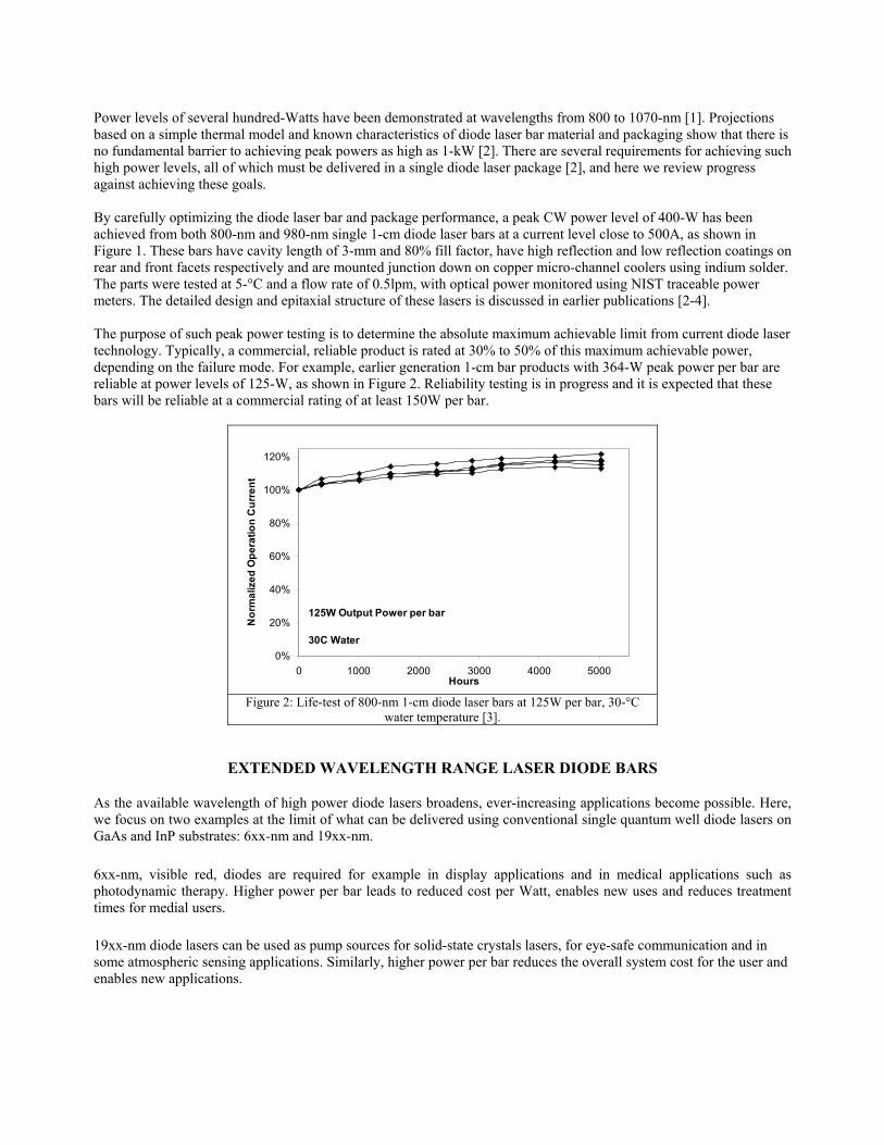
Power levels of several hundred-Watts have been demonstrated at wavelengths from 800 to 1070-nm [1]. Projections based on a simple thermal model and known characteristics of diode laser bar material and packaging show that there is no fundamental barrier to achieving peak powers as high as 1-kW [2]. There are several requirements for achieving such high power levels, all of which must be delivered in a single diode laser package [2], and here we review progress against achieving these goals. By carefully optimizing the diode laser bar and package performance, a peak CW power level of 400-W has been achieved from both 800-nm and 980-nm single 1-cm diode laser bars at a current level close to 500A, as shown in Figure 1. These bars have cavity length of 3-mm and 80% fill factor, have high reflection and low reflection coatings on rear and front facets respectively and are mounted junction down on copper micro-channel coolers using indium solder. The parts were tested at 5-°C and a flow rate of 0.5lpm, with optical power monitored using NIST traceable power meters. The detailed design and epitaxial structure of these lasers is discussed in earlier publications [2-4]. The purpose of such peak power testing is to determine the absolute maximum achievable limit from current diode laser technology. Typically, a commercial, reliable product is rated at 30% to 50% of this maximum achievable power, depending on the failure mode. For example, earlier generation 1-cm bar products with 364-W peak power per bar are reliable at power levels of 125-W, as shown in Figure 2. Reliability testing is in progress and it is expected that these bars will be reliable at a commercial rating of at least 150W per bar.
0%
20%
40%
60%
80%
100%
120%
0 1000 2000 3000 4000 5000Hours
Nor
mal
ized
Ope
ratio
n C
urre
nt
125W Output Power per bar
30C Water
Figure 2: Life-test of 800-nm 1-cm diode laser bars at 125W per bar, 30-°C
water temperature [3].
EXTENDED WAVELENGTH RANGE LASER DIODE BARS
As the available wavelength of high power diode lasers broadens, ever-increasing applications become possible. Here, we focus on two examples at the limit of what can be delivered using conventional single quantum well diode lasers on GaAs and InP substrates: 6xx-nm and 19xx-nm.
6xx-nm, visible red, diodes are required for example in display applications and in medical applications such as photodynamic therapy. Higher power per bar leads to reduced cost per Watt, enables new uses and reduces treatment times for medial users. 19xx-nm diode lasers can be used as pump sources for solid-state crystals lasers, for eye-safe communication and in some atmospheric sensing applications. Similarly, higher power per bar reduces the overall system cost for the user and enables new applications.
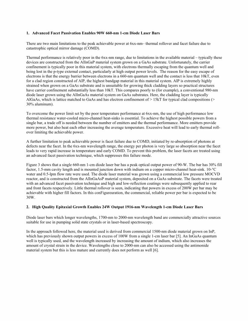
1. Advanced Facet Passivation Enables 90W 660-nm 1-cm Diode Laser Bars There are two main limitations to the peak achievable power at 6xx-nm– thermal rollover and facet failure due to catastrophic optical mirror damage (COMD). Thermal performance is relatively poor in the 6xx-nm range, due to limitations in the available material – typically these devices are constructed from the AlInGaP material system grown on a GaAs substrate. Unfortunately, the carrier confinement is typically poor in this material system, with electrons thermally escaping from the quantum well and being lost in the p-type external contact, particularly at high output power levels. The reason for the easy escape of electrons is that the energy barrier between electrons in a 660-nm quantum well and the contact is less that 10kT, even for a clad region constructed of AlP, the highest bandgap material in this material system. AlP is extremely highly strained when grown on a GaAs substrate and is unsuitable for growing thick cladding layers so practical structures have carrier confinement substantially less than 10kT. This compares poorly to (for example), a conventional 980-nm diode laser grown using the AlInGaAs material system on GaAs substrates. Here, the cladding layer is typically AlGaAs, which is lattice matched to GaAs and has electron confinement of > 15kT for typical clad compositions (> 30% aluminum). To overcome the power limit set by the poor temperature performance at 6xx-nm, the use of high performance low thermal resistance water-cooled micro-channel heat-sinks is essential. To achieve the highest possible powers from a single bar, a trade off is needed between the number of emitters and the thermal performance. More emitters provide more power, but also heat each other increasing the average temperature. Excessive heat will lead to early thermal roll-over limiting the achievable power. A further limitation to peak achievable power is facet failure due to COMD, initiated by re-absorption of photons at defects near the facet. In the 6xx-nm wavelength range, the energy per photon is very large so absorption near the facet leads to very rapid increase in temperature and early COMD. To prevent this problem, the laser facets are treated using an advanced facet passivation technique, which suppresses this failure mode. Figure 3 shows that a single 660-nm 1-cm diode laser bar has a peak optical output power of 90-W. The bar has 30% fill factor, 1.5-mm cavity length and is mounted junction down with indium on a copper micro-channel heat-sink. 10-°C water and 0.5-lpm flow rate were used. The diode laser material was grown using a commercial low pressure MOCVD reactor, and is constructed from the AlInGaAsP material system, deposited on a GaAs substrate. The facets were treated with an advanced facet passivation technique and high and low-reflection coatings were subsequently applied to rear and front facets respectively. Little thermal rollover is seen, indicating that powers in excess of 200W per bar may be achievable with higher fill factors. In this conFigureuration, the commercial, reliable power per bar is expected to be 30W.
2. High Quality Epitaxial Growth Enables 24W Output 1916-nm Wavelength 1-cm Diode Laser Bars Diode laser bars which longer wavelengths, 1700-nm to 2000-nm wavelength band are commercially attractive sources suitable for use in pumping solid state crystals or in laser-based spectroscopy. In the approach followed here, the material used is derived from commercial 1500-nm diode material grown on InP, which has previously shown output powers in excess of 100W from a single 1-cm laser bar [5]. An InGaAs quantum well is typically used, and the wavelength increased by increasing the amount of indium, which also increases the amount of crystal strain in the device. Wavelengths close to 2000-nm can also be accessed using the antimonide material system but this is less mature and currently does not perform as well [6].
There are two main limitations to generating high performance material at this wavelength. First and foremost is the impact of high strain levels. Low levels of crystal strain are typically beneficial to laser performance. However, at very high strain levels, the crystal will deform and defects build up (the strain “relaxes”), degrading performance and lifetime. Careful control of the growth conditions is required to minimize the impact of high strain levels [6]. Secondly, as wavelength increases, performance is increasingly limited by carrier loss due to Auger recombination, which degrades threshold current and temperature performance – for example the Auger recombination rate increases by a factor of ~10 when wavelength is increased from 1.5um to 2um [6]. To limit the impact of Auger recombination, designs are selected which minimize threshold current. The use of a high performance micro-channel heat-sink is also essential. In Figure 3, a single 1900-nm 1-cm diode laser bar is shown to have a peak optical output power of 23.5W. The bar has 20% fill factor, 1.0mm cavity length and is mounted junction down with indium on a copper micro-channel heat-sink. 5-°C water and 0.5lpm flow rate were used. The diode laser material was grown using a commercial low pressure MOCVD reactor, and the InGaAsP material system was used, deposited on an InP substrate. High and low-reflection coatings were subsequently applied to rear and front facets respectively. Thermal rollover limits the peak power of the bar.
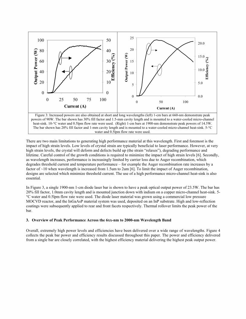
3. Overview of Peak Performance Across the 6xx-nm to 2000-nm Wavelength Band Overall, extremely high power levels and efficiencies have been delivered over a wide range of wavelengths. Figure 4 collects the peak bar power and efficiency results discussed throughout this paper. The power and efficiency delivered from a single bar are closely correlated, with the highest efficiency material delivering the highest peak output power.
0
20
40
60
80
100
0 25 50 75 100Current (A)
Out
put P
ower
(W)
0
10
20
30
40
50
Effi
cien
cy (%
)
0
5
10
15
20
25
0 50 100
Current (A)
Out
put P
ower
(W)
0.0
5.0
10.0
15.0
20.0
Eff
icie
ncy
(%)
Figure 3: Increased powers are also obtained at short and long wavelengths (left) 1-cm bars at 660-nm demonstrate peak
powers of 90W. The bar shown has 30% fill factor and 1.5-mm cavity length and is mounted to a water-cooled micro-channel heat-sink. 10-°C water and 0.5lpm flow rate were used. (Right) 1-cm bars at 1900-nm demonstrate peak powers of 14.5W. The bar shown has 20% fill factor and 1-mm cavity length and is mounted to a water-cooled micro-channel heat-sink. 5-°C
water and 0.5lpm flow rate were used.
0
25
50
75
100
500 750 1000 1250 1500 1750 2000Wavelength (nm)
Eff
icie
ncy
(%)
1
10
100
1000
Peak
Bar
Pow
er (W
)
Peak EfficiencyPeak Bar Power
Figure 4: Compiled material efficiency and peak bar power on across
wavelength
PATH TO 1KW PEAK CW OPTICAL OUTPUT PER BAR There are two main reasons for increasing the power achievable from 1-cm laser bar. The increased power density will enable new applications, for example in direct material processing. Also, the increased power per bar will lead to lower cost to the user, per watt of useable output. Following the rule of thumb that reliable power is ~ 30% - 50% of the peak power, a reliable 300-W bar will require a peak output of 600-W to 900-W. A careful analysis of the path to a 1-kW bar confirms that it is physically realistic using currently available materials and helps focus development efforts on the correct areas. Here, the main requirements for very high powers are reviewed and progress against these is discussed.
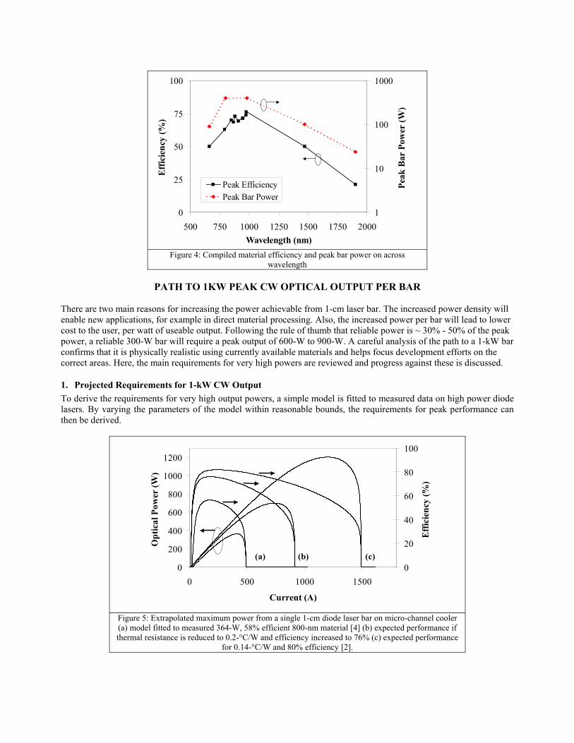
1. Projected Requirements for 1-kW CW Output To derive the requirements for very high output powers, a simple model is fitted to measured data on high power diode lasers. By varying the parameters of the model within reasonable bounds, the requirements for peak performance can then be derived.
0
200
400
600
800
1000
1200
0 500 1000 1500
Current (A)
Opt
ical
Pow
er (W
)
0
20
40
60
80
100
Effi
cien
cy (%
)
(a) (b) (c)
Figure 5: Extrapolated maximum power from a single 1-cm diode laser bar on micro-channel cooler (a) model fitted to measured 364-W, 58% efficient 800-nm material [4] (b) expected performance if thermal resistance is reduced to 0.2-°C/W and efficiency increased to 76% (c) expected performance
for 0.14-°C/W and 80% efficiency [2].
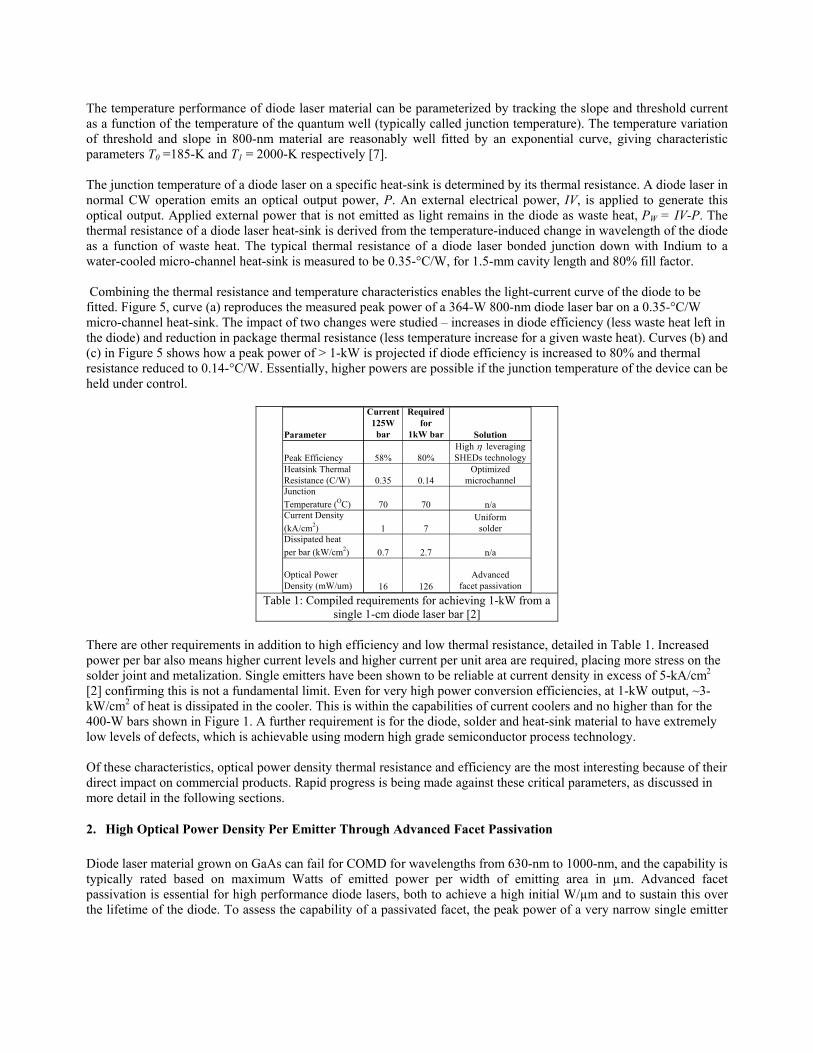
The temperature performance of diode laser material can be parameterized by tracking the slope and threshold current as a function of the temperature of the quantum well (typically called junction temperature). The temperature variation of threshold and slope in 800-nm material are reasonably well fitted by an exponential curve, giving characteristic parameters T0 =185-K and T1 = 2000-K respectively [7]. The junction temperature of a diode laser on a specific heat-sink is determined by its thermal resistance. A diode laser in normal CW operation emits an optical output power, P. An external electrical power, IV, is applied to generate this optical output. Applied external power that is not emitted as light remains in the diode as waste heat, PW = IV-P. The thermal resistance of a diode laser heat-sink is derived from the temperature-induced change in wavelength of the diode as a function of waste heat. The typical thermal resistance of a diode laser bonded junction down with Indium to a water-cooled micro-channel heat-sink is measured to be 0.35-°C/W, for 1.5-mm cavity length and 80% fill factor. Combining the thermal resistance and temperature characteristics enables the light-current curve of the diode to be fitted. Figure 5, curve (a) reproduces the measured peak power of a 364-W 800-nm diode laser bar on a 0.35-°C/W micro-channel heat-sink. The impact of two changes were studied – increases in diode efficiency (less waste heat left in the diode) and reduction in package thermal resistance (less temperature increase for a given waste heat). Curves (b) and (c) in Figure 5 shows how a peak power of > 1-kW is projected if diode efficiency is increased to 80% and thermal resistance reduced to 0.14-°C/W. Essentially, higher powers are possible if the junction temperature of the device can be held under control.
Parameter
Current125W
bar
Required for
1kW bar Solution
Peak Efficiency 58% 80%High η leveraging SHEDs technology
Heatsink ThermalResistance (C/W) 0.35 0.14
Optimizedmicrochannel
Junction Temperature (OC) 70 70 n/aCurrent Density(kA/cm2) 1 7
Uniformsolder
Dissipated heat per bar (kW/cm2) 0.7 2.7 n/a
Optical PowerDensity (mW/um) 16 126
Advanced facet passivation
Table 1: Compiled requirements for achieving 1-kW from a single 1-cm diode laser bar [2]
There are other requirements in addition to high efficiency and low thermal resistance, detailed in Table 1. Increased power per bar also means higher current levels and higher current per unit area are required, placing more stress on the solder joint and metalization. Single emitters have been shown to be reliable at current density in excess of 5-kA/cm2 [2] confirming this is not a fundamental limit. Even for very high power conversion efficiencies, at 1-kW output, ~3-kW/cm2 of heat is dissipated in the cooler. This is within the capabilities of current coolers and no higher than for the 400-W bars shown in Figure 1. A further requirement is for the diode, solder and heat-sink material to have extremely low levels of defects, which is achievable using modern high grade semiconductor process technology. Of these characteristics, optical power density thermal resistance and efficiency are the most interesting because of their direct impact on commercial products. Rapid progress is being made against these critical parameters, as discussed in more detail in the following sections.
2. High Optical Power Density Per Emitter Through Advanced Facet Passivation Diode laser material grown on GaAs can fail for COMD for wavelengths from 630-nm to 1000-nm, and the capability is typically rated based on maximum Watts of emitted power per width of emitting area in µm. Advanced facet passivation is essential for high performance diode lasers, both to achieve a high initial W/µm and to sustain this over the lifetime of the diode. To assess the capability of a passivated facet, the peak power of a very narrow single emitter

device (or low fill factor bar) is measured. As an example, results for a 50-µm stripe, 1.5mm cavity 800-nm diode laser are shown in Figure 6. The device was bonded junction down on industry standard c-mount and measured to peak power at 10-°C heat-sink temperature. The facets were passivated then coated with high reflection and low reflection coatings. A peak power of 7-W was reached, equivalent to 140-mW/µm. In comparison, a 1-kW diode laser bar would deliver 126-mW/µm of output, below this level.
0
20
40
60
80
100
120
140
160
0 2 4 6 8 10 12 14
Current Density (kA/cm2)
Out
put p
ower
per
um
(mW
)
Figure 6: A single 50-µm stripe 800-nm device on c-
mount will rollover at 7-W (140-mW/µm) when appropriate facet passivation is used [2].
3. Low Thermal Resistance Using Optimized Micro-channel Cooler The thermal resistance of a water-cooled micro-channel cooler is controlled by three effects – the properties of the coolant, the properties of the metal used to construct the cooler and the design of the micro-channels within the cooler. Without changing the coolant or metal (water and copper), optimizing the design of the micro-channels within the cooler is found to reduce the thermal resistance to 0.17-°C/W, as shown in Figure 7. The change in junction temperature is derived from the changes in the laser wavelength as operation current is increased (scaled by the known temperature characteristic at 800-nm of 0.28-nm/C). The waste heat is directly measured. The results in Figure 7 were obtained from the 3-mm cavity length bar shown in Figure 1. The increased device length enabled the micro-channel design to be re-optimized for increased performance. This is not sufficient for 1-kW operation but is significant progress.
y = 0.1746x
0
5
10
15
20
25
30
0 50 100 150
Waste heat (W)
Cha
nge
in
Junc
tion
Tem
pera
ture
(°C
)
Figure 7: An optimized micro-channel cooler is
measured to have thermal resistance of 0.17-°C/W.
4. Diode Material and Design Optimization for High Efficiency
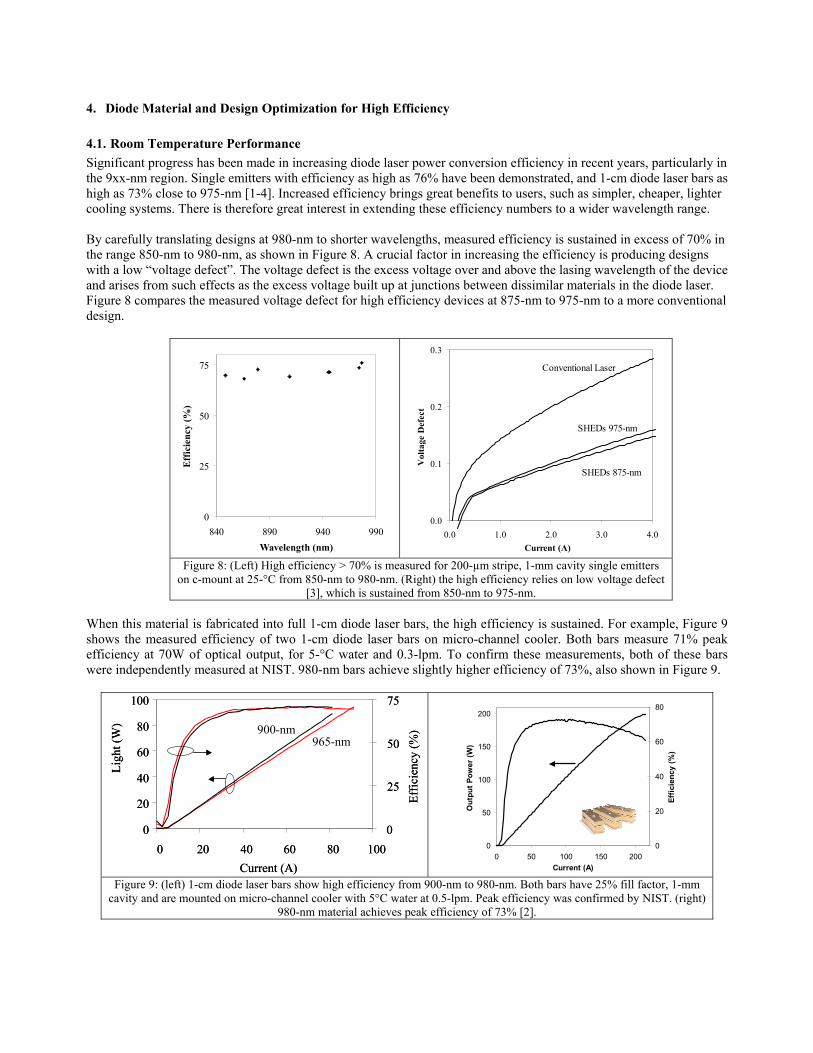
4.1. Room Temperature Performance Significant progress has been made in increasing diode laser power conversion efficiency in recent years, particularly in the 9xx-nm region. Single emitters with efficiency as high as 76% have been demonstrated, and 1-cm diode laser bars as high as 73% close to 975-nm [1-4]. Increased efficiency brings great benefits to users, such as simpler, cheaper, lighter cooling systems. There is therefore great interest in extending these efficiency numbers to a wider wavelength range. By carefully translating designs at 980-nm to shorter wavelengths, measured efficiency is sustained in excess of 70% in the range 850-nm to 980-nm, as shown in Figure 8. A crucial factor in increasing the efficiency is producing designs with a low “voltage defect”. The voltage defect is the excess voltage over and above the lasing wavelength of the device and arises from such effects as the excess voltage built up at junctions between dissimilar materials in the diode laser. Figure 8 compares the measured voltage defect for high efficiency devices at 875-nm to 975-nm to a more conventional design.
0
25
50
75
840 890 940 990Wavelength (nm)
Effic
ienc
y (%
)
0.0
0.1
0.2
0.3
0.0 1.0 2.0 3.0 4.0Current (A)
Vol
tage
Def
ect
Conventional Laser
SHEDs 975-nm
SHEDs 875-nm
Figure 8: (Left) High efficiency > 70% is measured for 200-µm stripe, 1-mm cavity single emitters
on c-mount at 25-°C from 850-nm to 980-nm. (Right) the high efficiency relies on low voltage defect [3], which is sustained from 850-nm to 975-nm.
When this material is fabricated into full 1-cm diode laser bars, the high efficiency is sustained. For example, Figure 9 shows the measured efficiency of two 1-cm diode laser bars on micro-channel cooler. Both bars measure 71% peak efficiency at 70W of optical output, for 5-°C water and 0.3-lpm. To confirm these measurements, both of these bars were independently measured at NIST. 980-nm bars achieve slightly higher efficiency of 73%, also shown in Figure 9.
0
20
40
60
80
100
0 20 40 60 80 100Current (A)
Ligh
t (W
)
0
25
50
75
Effic
ienc
y (%
)
965-nm900-nm
0
20
40
60
80
100
0 20 40 60 80 100Current (A)
Ligh
t (W
)
0
25
50
75
Effic
ienc
y (%
)
965-nm900-nm
0
50
100
150
200
0 50 100 150 200Current (A)
Out
put P
ower
(W)
0
20
40
60
80
Effic
ienc
y (%
)
Figure 9: (left) 1-cm diode laser bars show high efficiency from 900-nm to 980-nm. Both bars have 25% fill factor, 1-mm
cavity and are mounted on micro-channel cooler with 5°C water at 0.5-lpm. Peak efficiency was confirmed by NIST. (right) 980-nm material achieves peak efficiency of 73% [2].
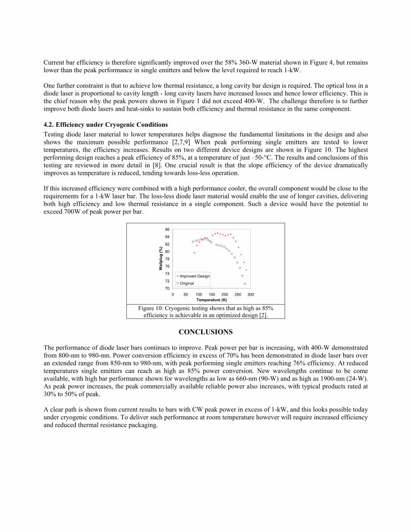
Current bar efficiency is therefore significantly improved over the 58% 360-W material shown in Figure 4, but remains lower than the peak performance in single emitters and below the level required to reach 1-kW. One further constraint is that to achieve low thermal resistance, a long cavity bar design is required. The optical loss in a diode laser is proportional to cavity length - long cavity lasers have increased losses and hence lower efficiency. This is the chief reason why the peak powers shown in Figure 1 did not exceed 400-W. The challenge therefore is to further improve both diode lasers and heat-sinks to sustain both efficiency and thermal resistance in the same component.
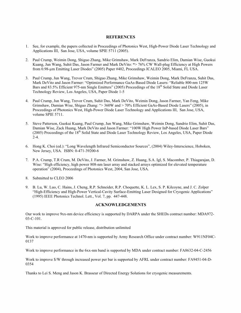
4.2. Efficiency under Cryogenic Conditions Testing diode laser material to lower temperatures helps diagnose the fundamental limitations in the design and also shows the maximum possible performance [2,7,9] When peak performing single emitters are tested to lower temperatures, the efficiency increases. Results on two different device designs are shown in Figure 10. The highest performing design reaches a peak efficiency of 85%, at a temperature of just –50-°C. The results and conclusions of this testing are reviewed in more detail in [8]. One crucial result is that the slope efficiency of the device dramatically improves as temperature is reduced, tending towards loss-less operation. If this increased efficiency were combined with a high performance cooler, the overall component would be close to the requirements for a 1-kW laser bar. The loss-less diode laser material would enable the use of longer cavities, delivering both high efficiency and low thermal resistance in a single component. Such a device would have the potential to exceed 700W of peak power per bar.
70
72
74
76
78
80
82
84
86
0 50 100 150 200 250 300Temperature (K)
Wal
lplu
g (%
)
Improved Design
Original
Figure 10: Cryogenic testing shows that as high as 85%
efficiency is achievable in an optimized design [2].
CONCLUSIONS The performance of diode laser bars continues to improve. Peak power per bar is increasing, with 400-W demonstrated from 800-nm to 980-nm. Power conversion efficiency in excess of 70% has been demonstrated in diode laser bars over an extended range from 850-nm to 980-nm, with peak performing single emitters reaching 76% efficiency. At reduced temperatures single emitters can reach as high as 85% power conversion. New wavelengths continue to be come available, with high bar performance shown for wavelengths as low as 660-nm (90-W) and as high as 1900-nm (24-W). As peak power increases, the peak commercially available reliable power also increases, with typical products rated at 30% to 50% of peak. A clear path is shown from current results to bars with CW peak power in excess of 1-kW, and this looks possible today under cryogenic conditions. To deliver such performance at room temperature however will require increased efficiency and reduced thermal resistance packaging.
REFERENCES
1. See, for example, the papers collected in Proceedings of Photonics West, High-Power Diode Laser Technology and
Applications III, San Jose, USA, volume SPIE 5711 (2005). 2. Paul Crump, Weimin Dong, Shiguo Zhang, Mike Grimshaw, Mark DeFranza, Sandrio Elim, Damian Wise, Guokui
Kuang, Jun Wang, Suhit Das, Jason Farmer and Mark DeVito: “> 76% CW Wall-plug Efficiency at High Powers from 0.98-µm Emitting Laser Diodes” (2005) Paper #402, Proceedings ICALEO 2005, Miami, FL USA.
3. Paul Crump, Jun Wang, Trevor Crum, Shiguo Zhang, Mike Grimshaw, Weimin Dong, Mark DeFranza, Suhit Das,
Mark DeVito and Jason Farmer: “Optimized Performance GaAs-Based Diode Lasers: “Reliable 800-nm 125W Bars and 83.5% Efficient 975-nm Single Emitters” (2005) Proceedings of the 18th Solid State and Diode Laser Technology Review, Los Angeles, USA, Paper Diode 1-5
4. Paul Crump, Jun Wang, Trevor Crum, Suhit Das, Mark DeVito, Weimin Dong, Jason Farmer, Yan Feng, Mike
Grimshaw, Damian Wise, Shiguo Zhang: “> 360W and > 70% Efficient GaAs-Based Diode Lasers” (2005), in Proceedings of Photonics West, High-Power Diode Laser Technology and Applications III, San Jose, USA, volume SPIE 5711.
5. Steve Patterson, Guokui Kuang, Paul Crump, Jun Wang, Mike Grimshaw, Weimin Dong, Sandrio Elim, Suhit Das,
Damian Wise, Zack Huang, Mark DeVito and Jason Farmer: “100W High Power InP-based Diode Laser Bars” (2005) Proceedings of the 18th Solid State and Diode Laser Technology Review, Los Angeles, USA, Paper Diode 2-4.
6. Hong K. Choi (ed.): “Long Wavelength Infrared Semiconductor Sources”, (2004) Wiley-Interscience, Hoboken,
New Jersey, USA. ISBN: 0-471-39200-6 7. P.A. Crump, T.R Crum, M. DeVito, J. Farmer, M. Grimshaw, Z. Huang, S.A. Igl, S. Macomber, P. Thiagarajan, D.
Wise: “High efficiency, high power 808-nm laser array and stacked arrays optimized for elevated temperature operation” (2004), Proceedings of Photonics West, 2004, San Jose, USA.
8. Submitted to CLEO 2006 9. B. Lu, W. Luo, C. Hains, J. Cheng, R.P. Schneider, R.P. Choquette, K. L. Lex, S. P. Kilcoyne, and J. C. Zolper
“High-Efficiency and High-Power Vertical-Cavity Surface-Emitting Laser Designed for Cryogenic Applications” (1995) IEEE Photonics Technol. Lett., Vol. 7, pp. 447-448.
ACKNOWLEDGEMENTS
Our work to improve 9xx-nm device efficiency is supported by DARPA under the SHEDs contract number: MDA972-03-C-101. This material is approved for public release, distribution unlimited Work to improve performance at 1470-nm is supported by Army Research Office under contract number: W911NF04C-0137 Work to improve performance in the 6xx-nm band is supported by MDA under contract number: FA8632-04-C-2456 Work to improve $/W through increased power per bar is supported by AFRL under contract number: FA9451-04-D-0354 Thanks to Lei S. Meng and Jason K. Brasseur of Directed Energy Solutions for cryogenic measurements.
Copyright © 2022 FDOKUMEN