Development System Reference Guide Design Flow Design Flow Overview
24
Development System Reference Guide www.xilinx.com 31 R Chapter 2 Design Flow This chapter describes the process for creating, implementing, verifying, and downloading designs for FPGA and CPLD devices. For a complete description of FPGAs and CPLDs, refer to the Xilinx Data Sheets at http://www.xilinx.com/xlnx/xweb/xil_publications_index.jsp This chapter contains the following sections: • “Design Flow Overview” • “Design Entry and Synthesis” • “Design Implementation” • “Design Verification” • “FPGA Design Tips” Design Flow Overview The standard design flow comprises the following steps: 1. Design Entry and Synthesis—In this step of the design flow, you create your design using a Xilinx-supported schematic editor, a hardware description language (HDL) for text-based entry, or both. If you use an HDL for text-based entry, you must synthesize the HDL file into an EDIF file or, if you are using the Xilinx Synthesis Technology (XST) GUI, you must synthesize the HDL file into an NGC file. 2. Design Implementation—By implementing to a specific Xilinx architecture, you convert the logical design file format, such as EDIF, that you created in the design entry and synthesis stage into a physical file format. The physical information is contained in the native circuit description (NCD) file for FPGAs and the VM6 file for CPLDs. Then you create a bitstream file from these files and optionally program a PROM or EPROM for subsequent programming of your Xilinx device. 3. Design Verification—Using a gate-level simulator or cable, you ensure that your design meets your timing requirements and functions properly. See the iMPACT online help for information about Xilinx download cables and demonstration boards. The full design flow is an iterative process of entering, implementing, and verifying your design until it is correct and complete. The Xilinx Development System allows quick design iterations through the design flow cycle. Because Xilinx devices permit unlimited reprogramming, you do not need to discard devices when debugging your design in circuit.
Transcript of Development System Reference Guide Design Flow Design Flow Overview

R
Chapter 2
Design Flow
This chapter describes the process for creating, implementing, verifying, and downloading designs for FPGA and CPLD devices. For a complete description of FPGAs and CPLDs, refer to the Xilinx Data Sheets at http://www.xilinx.com/xlnx/xweb/xil_publications_index.jsp
This chapter contains the following sections:
• “Design Flow Overview”
• “Design Entry and Synthesis”
• “Design Implementation”
• “Design Verification”
• “FPGA Design Tips”
Design Flow OverviewThe standard design flow comprises the following steps:
1. Design Entry and Synthesis—In this step of the design flow, you create your design using a Xilinx-supported schematic editor, a hardware description language (HDL) for text-based entry, or both. If you use an HDL for text-based entry, you must synthesize the HDL file into an EDIF file or, if you are using the Xilinx Synthesis Technology (XST) GUI, you must synthesize the HDL file into an NGC file.
2. Design Implementation—By implementing to a specific Xilinx architecture, you convert the logical design file format, such as EDIF, that you created in the design entry and synthesis stage into a physical file format. The physical information is contained in the native circuit description (NCD) file for FPGAs and the VM6 file for CPLDs. Then you create a bitstream file from these files and optionally program a PROM or EPROM for subsequent programming of your Xilinx device.
3. Design Verification—Using a gate-level simulator or cable, you ensure that your design meets your timing requirements and functions properly. See the iMPACT online help for information about Xilinx download cables and demonstration boards.
The full design flow is an iterative process of entering, implementing, and verifying your design until it is correct and complete. The Xilinx Development System allows quick design iterations through the design flow cycle. Because Xilinx devices permit unlimited reprogramming, you do not need to discard devices when debugging your design in circuit.
Development System Reference Guide www.xilinx.com 31
Chapter 2: Design FlowR
In addition to the standard design flow described in this chapter, you can break your design into modules for use with one or more of the hierarchical flows, which are Modular Design, Incremental Design, and Partial Reconfiguration. These hierarchical flows are useful when performing team-based and incremental design, and when you want to reconfigure one part of your design. When using the hierarchical flows, it is important that your design follow good hierarchical design practices, as described in the “Hierarchical Design” section of this chapter.
The following figure shows the standard Xilinx design flow.
Figure 2-1: Xilinx Design Flow
X9537
DesignImplementation
Optimization
FPGAs
MappingPlacementRouting
CPLDs
Fitting
BitstreamGeneration
DesignSynthesis
DesignEntry
Download to aXilinx Device
Design Verification
FunctionalSimulation
Static TimingAnalysis
TimingSimulation
BackAnnotation
In-CircuitVerification
32 www.xilinx.com Development System Reference Guide

Design Flow OverviewR
The following figure shows the Xilinx software flow chart for FPGA designs.
Figure 2-2: Xilinx Software Design Flow (FPGAs)
X10293
V &SDF 2.1
VHD &SDF 2.1
SimulationLibraries
CORE Generator
Schematic Capture
Constraints Editor NGD
UCF
HDL
Symbol
NetGenNGM & PCF
EDIF2 0 0
MAPFloorplanner
NGC
TRACE &Timing Analyzer
PAR
BitGen
Synthesis Simulation
EDIF 2 0 0 &Constraints/NCF
NGC(XST Netlist)
NetGen
TestbenchStimulus
NCD & PCF
NCD
NGDBuild NGDBuildNGDBuild
SynthesisLibraries
SchematicLibraries
BIT
iMPACT
PROMGen
Development System Reference Guide www.xilinx.com 33
Chapter 2: Design FlowR
The following figure shows the Xilinx software flow chart for CPLD designs.
Figure 2-3: Xilinx Software Design Flow (CPLDs)
X10294
V &SDF 2.1
VHD &SDF 2.1
SimulationLibraries
CORE Generator
Schematic Capture
NGD
HDL
Symbol
GYD
EDIF2 0 0
CPLD Fitter
NGC
JED VM6
iMPACT Timing Analyzer
Synthesis Simulation
EDIF 2 0 0 &Constraints/NCF
NGC(XST Netlist)
NetGen
TestbenchStimulus
NGDBuild NGDBuildNGDBuild
SynthesisLibraries
SchematicLibraries
34 www.xilinx.com Development System Reference Guide

Design Entry and SynthesisR
Design Entry and SynthesisYou can enter a design with a schematic editor or a text-based tool. Design entry begins with a design concept, expressed as a drawing or functional description. From the original design, a netlist is created, then synthesized and translated into a native generic object (NGO) file. This file is fed into the Xilinx software program called NGDBuild, which produces a logical native generic database (NGD) file.
The following figure shows the design entry and synthesis process.
Hierarchical DesignDesign hierarchy is important in both schematic and HDL entry for the following reasons:
• Helps you conceptualize your design
• Adds structure to your design
• Promotes easier design debugging
• Makes it easier to combine different design entry methods (schematic, HDL, or state editor) for different parts of your design
• Makes it easier to design incrementally, which consists of designing, implementing, and verifying individual parts of a design in stages
• Reduces optimization time
• Facilitates concurrent design, which is the process of dividing a design among a number of people who develop different parts of the design in parallel, such as in Modular Design
Figure 2-4: Design Entry Flow
X10295
CORE Generator
Schematic Capture
UCFNGC
(XST Netlist)
HDL
Synthesis
EDIF 2 0 0 &Constraints/NCF
SchematicLibraries
SynthesisLibraries
NGDBuild
Development System Reference Guide www.xilinx.com 35

Chapter 2: Design FlowR
In hierarchical designing, a specific hierarchical name identifies each library element, unique block, and instance you create. The following example shows a hierarchical name with a 2-input OR gate in the first instance of a multiplexer in a 4-bit counter:
/Acc/alu_1/mult_4/8count_3/4bit_0/mux_1/or2
Xilinx strongly recommends that you name the components and nets in your design. These names are preserved and used by the FPGA Editor tool. These names are also used for back-annotation and appear in the debug and analysis tools. If you do not name your components and nets, the schematic editor automatically generates the names. For example, if left unnamed, the software might name the previous example, as follows:
/$1a123/$1b942/$1c23/$1d235/$1e121/$1g123/$1h57
Note: It is difficult to analyze circuits with automatically generated names, because the names only have meaning for Xilinx software.
Schematic Entry OverviewSchematic tools provide a graphic interface for design entry. You can use these tools to connect symbols representing the logic components in your design. You can build your design with individual gates, or you can combine gates to create functional blocks. This section focuses on ways to enter functional blocks using library elements and the CORE Generator.
Library Elements
Primitives and macros are the “building blocks” of component libraries. Xilinx libraries provide primitives, as well as common high-level macro functions. Primitives are basic circuit elements, such as AND and OR gates. Each primitive has a unique library name, symbol, and description. Macros contain multiple library elements, which can include primitives and other macros.
You can use the following types of macros with Xilinx FPGAs:
• Soft macros have pre-defined functionality but have flexible mapping, placement, and routing. Soft macros are available for all FPGAs.
• Relationally placed macros (RPMs) have fixed mapping and relative placement. RPMs are available for all device families, except the XC9500 family.
Macros are not available for synthesis because synthesis tools have their own module generators and do not require RPMs. If you wish to override the module generation, you can instantiate CORE Generator modules. For most leading-edge synthesis tools, this does not offer an advantage unless it is for a module that cannot be inferred.
CORE Generator Tool (FPGAs Only)
The Xilinx CORE Generator design tool delivers parameterizable cores that are optimized for Xilinx FPGAs. The library includes cores ranging from simple delay elements to complex DSP (Digital Signal Processing) filters and multiplexers. For details, refer to the CORE Generator Guide. You can also refer to the Xilinx IP (Intellectual Property) Center Web site at http://www.xilinx.com/ipcenter, which offers the latest IP solutions. These solutions include design reuse tools, free reference designs, DSP and PCI solutions, IP implementation tools, cores, specialized system level services, and vertical application IP solutions.
36 www.xilinx.com Development System Reference Guide

Design Entry and SynthesisR
HDL Entry and SynthesisA typical Hardware Description Language (HDL) supports a mixed-level description in which gate and netlist constructs are used with functional descriptions. This mixed-level capability enables you to describe system architectures at a high level of abstraction, then incrementally refine the detailed gate-level implementation of a design.
HDL descriptions offer the following advantages:
• You can verify design functionality early in the design process. A design written as an HDL description can be simulated immediately. Design simulation at this high level, at the gate-level before implementation, allows you to evaluate architectural and design decisions.
• An HDL description is more easily read and understood than a netlist or schematic description. HDL descriptions provide technology-independent documentation of a design and its functionality. Because the initial HDL design description is technology independent, you can use it again to generate the design in a different technology, without having to translate it from the original technology.
• Large designs are easier to handle with HDL tools than schematic tools.
After you create your HDL design, you must synthesize it. During synthesis, behavioral information in the HDL file is translated into a structural netlist, and the design is optimized for a Xilinx device. Xilinx supports HDL synthesis tools for several third-party synthesis vendors. In addition, Xilinx offers its own synthesis tool, Xilinx Synthesis Technology (XST). See the Xilinx Synthesis Technology (XST) User Guide for information. For detailed information on synthesis, see the Synthesis and Verification Design Guide.
Functional SimulationAfter you create your design, you can simulate it. Functional simulation tests the logic in your design to determine if it works properly. You can save time during subsequent design steps if you perform functional simulation early in the design flow. See “Simulation” for more information.
ConstraintsYou may want to constrain your design within certain timing or placement parameters. You can specify mapping, block placement, and timing specifications.
You can enter constraints manually or use the Constraints Editor, Floorplanner, or FPGA Editor, which are graphical user interface (GUI) tools provided by Xilinx. You can use the Timing Analyzer GUI or TRACE command line program to evaluate the circuit against these constraints by generating a static timing analysis of your design. See Chapter 14, “TRACE” and the online Help provided with each GUI for information. See the Constraints Guide for detailed information on constraints.
Mapping Constraints (FPGAs Only)
You can specify how a block of logic is mapped into CLBs using an FMAP for all Spartan FPGA and Virtex FPGA families. These mapping symbols can be used in your schematic. However, if you overuse these specifications, it may be difficult to route your design.
Development System Reference Guide www.xilinx.com 37
Chapter 2: Design FlowR
Block Placement
Block placement can be constrained to a specific location, to one of multiple locations, or to a location range. Locations can be specified in the schematic, with synthesis tools, or in the User Constraints File (UCF). Poor block placement can adversely affect both the placement and the routing of a design. Only I/O blocks require placement to meet external pin requirements.
Timing Specifications
You can specify timing requirements for paths in your design. PAR uses these timing specifications to achieve optimum performance when placing and routing your design.
Netlist Translation ProgramsTwo netlist translation programs allow you to read netlists into the Xilinx software tools. EDIF2NGD allows you to read an Electronic Data Interchange Format (EDIF) 2 0 0 file. The NGDBuild program automatically invokes these programs as needed to convert your EDIF file to an NGD file, the required format for the Xilinx software tools. NGC files output from the Xilinx XST synthesis tool are read in by NGDBuild directly.
You can find detailed descriptions of the EDIF2NGD, and NGDBuild programs in Chapter 8, “NGDBuild” and “Appendix B”.
Design ImplementationDesign Implementation begins with the mapping or fitting of a logical design file to a specific device and is complete when the physical design is successfully routed and a bitstream is generated. You can alter constraints during implementation just as you did during the Design Entry step. See “Constraints” for information.
38 www.xilinx.com Development System Reference Guide
Design ImplementationR
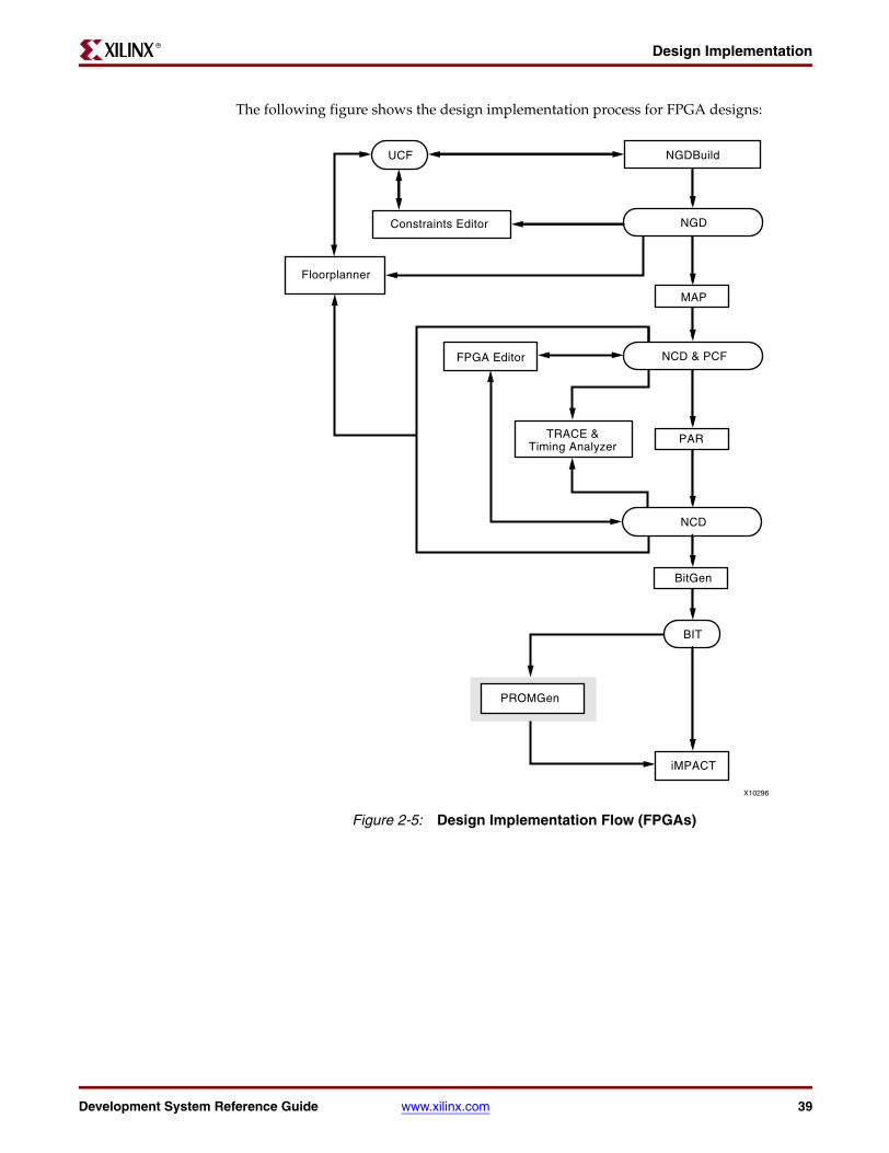
The following figure shows the design implementation process for FPGA designs:
Figure 2-5: Design Implementation Flow (FPGAs)
X10296
Constraints Editor NGD
UCF
BIT
MAP
Floorplanner
TRACE &Timing Analyzer
PAR
iMPACT
PROMGen
BitGen
NCD
NGDBuild
FPGA Editor NCD & PCF
Development System Reference Guide www.xilinx.com 39

Chapter 2: Design FlowR
The following figure shows the design implementation process for CPLD designs:
Figure 2-6: Design Implementation Flow (CPLDs)
X9493
Design Loader
NGDBuild
NGD
Auto Device/Speed Selector
Logic SynthesisTechnology Mapping
Global Net Optimization
Logic Optimization Partitioning
ExportingAssignments
Export Level Generator
PTerm Mapping
Power/Slew Optimization
Post-MappingEnhancements
Routing
CPLD FitterImplementation Options
RPT GYD
Pin Feedback Generation
Fitter Report (Text)
JED
HPLUSAS6
HPREP6
iMPACT
VM6
VM6
40 www.xilinx.com Development System Reference Guide
Design ImplementationR
Mapping (FPGAs Only)For FPGAs, the MAP command line program maps a logical design to a Xilinx FPGA. The input to MAP is an NGD file, which contains a logical description of the design in terms of both the hierarchical components used to develop the design and the lower-level Xilinx primitives, and any number of NMC (hard placed-and-routed macro) files, each of which contains the definition of a physical macro. MAP then maps the logic to the components (logic cells, I/O cells, and other components) in the target Xilinx FPGA.
The output design from MAP is an NCD file, which is a physical representation of the design mapped to the components in the Xilinx FPGA. The NCD file can then be placed and routed, using the PAR command line program. See Chapter 9, “MAP” for detailed information.
Placing and Routing (FPGAs Only)For FPGAs, the PAR command line program takes a mapped NCD file as input, places and routes the design, and outputs a placed and routed NCD file, which is used by the bitstream generator, BitGen. The output NCD file can also act as a guide file when you reiterate placement and routing for a design to which minor changes have been made after the previous iteration. See Chapter 11, “PAR” for detailed information.
You can also use the FPGA Editor GUI tool to do the following:
• Place and route critical components before running automatic place and route tools on an entire design
• Modify placement and routing manually; the editor allows both automatic and manual component placement and routing
Note: For more information, see the online Help provided with the FPGA Editor.
Bitstream Generation (FPGAs Only)For FPGAs, the BitGen command line program produces a bitstream for Xilinx device configuration. BitGen takes a fully routed NCD file as its input and produces a configuration bitstream—a binary file with a .bit extension. The BIT file contains all of the configuration information from the NCD file defining the internal logic and interconnections of the FPGA, plus device-specific information from other files associated with the target device. See Chapter 16, “BitGen” for detailed information.
After you generate your BIT file, you can download it to a device using the iMPACT GUI. You can also format the BIT file into a PROM file using the PromGen command line program and then download it to a device using the iMPACT GUI. See Chapter 18, “PROMGen” of this guide or the iMPACT online help for more information.
Development System Reference Guide www.xilinx.com 41

Chapter 2: Design FlowR
Design VerificationDesign verification is testing the functionality and performance of your design. You can verify Xilinx designs in the following ways:
• Simulation (functional and timing)
• Static timing analysis
• In-circuit verification
The following table lists the different design tools used for each verification type.
Table 2-1: Verification Tools
Verification Type Tools
Simulation Third-party simulators (integrated and non-integrated)
Static Timing Analysis
TRACE (command line program)
Timing Analyzer (GUI)
Mentor Graphics® TAU and Innoveda BLAST software for use with the STAMP file format (for I/O timing verification only)
In-Circuit Verification Design Rule Checker (command line program)
Download cable
42 www.xilinx.com Development System Reference Guide

Design VerificationR
Design verification procedures should occur throughout your design process, as shown in the following figures.
Figure 2-7: Three Verification Methods of the Design Flow (FPGAs)
X9556
Static Timing Analysis
Input Stimulus
Simulation Netlist
Simulation
Xilinx FPGA
Design EntryIntegrated Tool
Functional SimulatorPaths
Timing Simulation Path
Simulation
Static Timing
In-Circuit Verification
In-Circuit Verification
Basic Design Flow
NGD
NCD
BitGen
BIT
Mapping, Placementand Routing
Translate toSimulator Format
Translate toSimulator Format
Back-Annotation
NGA
Translation
Development System Reference Guide www.xilinx.com 43

Chapter 2: Design FlowR
The following figure shows the verification methods of the design flow for CPLDs.
SimulationYou can run functional or timing simulation to verify your design. This section describes the back-annotation process that must occur prior to timing simulation. It also describes the functional and timing simulation methods for both schematic and HDL-based designs.
Back-Annotation
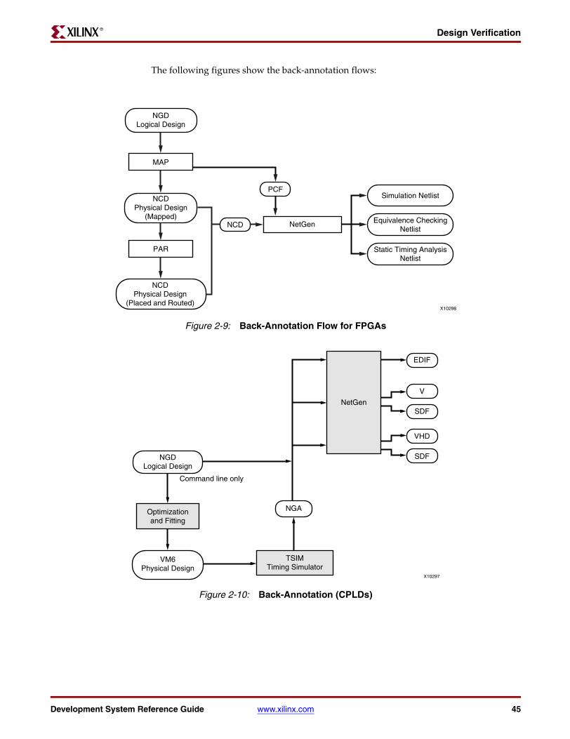
Before timing simulation can occur, the physical design information must be translated and distributed back to the logical design. For FPGAs, this back-annotation process is done with a program called NetGen. For CPLDs, back-annotation is performed with the TSim Timing Simulator. These programs create a database, which translates the back-annotated information into a netlist format that can be used for timing simulation.
Figure 2-8: Three Verification Methods of the Design Flow (CPLDs)
X9538
In-Circuit Verification
Static Timing Analysis
Input Stimulus
Simulation Netlist
Simulation
Xilinx CPLD
Design EntryIntegrated Tool
Functional SimulatorPaths
Timing Simulation Path
Simulation
Static Timing
In-Circuit Verification
Basic Design Flow
NGD
VM6
ProgrammingFile Creation
JED
Optimization andFitting
Translate toSimulator Format
Translate toSimulator Format
Back-Annotation
NGA
Translation
44 www.xilinx.com Development System Reference Guide
Design VerificationR
The following figures show the back-annotation flows:
Figure 2-9: Back-Annotation Flow for FPGAs
Figure 2-10: Back-Annotation (CPLDs)
X10298
PAR
NetGen
MAP
NGDLogical Design
NCDPhysical Design
(Mapped)
NCDPhysical Design
(Placed and Routed)
Simulation Netlist
Equivalence CheckingNetlist
Static Timing AnalysisNetlist
PCF
NCD
X10297
TSIMTiming Simulator
NetGen
Optimizationand Fitting
NGDLogical Design
VM6Physical Design
NGA
EDIF
VHD
SDF
SDF
V
Command line only
Development System Reference Guide www.xilinx.com 45
Chapter 2: Design FlowR
NetGen
NetGen is a command line program that distributes information about delays, setup and hold times, clock to out, and pulse widths found in the physical NCD design file back to the logical NGD file and generates a Verilog or VHDL netlist for use with supported timing simulation, equivalence checking, and static timing analysis tools.
NetGen reads an NCD as input. The NCD file can be a mapped-only design, or a partially or fully placed and routed design. An NGM file, created by MAP, is an optional source of input. NetGen merges mapping information from the optional NGM file with placement, routing, and timing information from the NCD file.
Note: NetGen reads an NGA file as input to generate a timing simulation netlist for CPLD designs.
See Chapter 24, “NetGen” for detailed information.
Schematic-Based Simulation
Design simulation involves testing your design using software models. It is most effective when testing the functionality of your design and its performance under worst-case conditions. You can easily probe internal nodes to check the behavior of your circuit, and then use these results to make changes in your schematic.
Simulation is performed using third-party tools that are linked to the Xilinx Development System. Use the various CAE-specific interface user guides, which cover the commands and features of the Xilinx-supported simulators, as your primary reference.
The software models provided for your simulation tools are designed to perform detailed characterization of your design. You can perform functional or timing simulation, as described in the following sections.
Functional Simulation
Functional simulation determines if the logic in your design is correct before you implement it in a device. Functional simulation can take place at the earliest stages of the design flow. Because timing information for the implemented design is not available at this stage, the simulator tests the logic in the design using unit delays.
Note: It is usually faster and easier to correct design errors if you perform functional simulation early in the design flow.
You can use integrated and non-integrated simulation tools. Integrated tools, such as Mentor Graphics or Innoveda, often contain a built-in interface that links the simulator and a schematic editor, allowing the tools to use the same netlist. You can move directly from entry to simulation when using a set of integrated tools.
Functional simulation in schematic-based tools is performed immediately after design entry in the capture environment. The schematic capture tool requires a Xilinx Unified Library and the simulator requires a library if the tools are not integrated. Most of the schematic-based tools require translation from their native database to EDIF for implementation. The return path from implementation is usually EDIF with certain exceptions in which a schematic tool is tied to an HDL simulator.
46 www.xilinx.com Development System Reference Guide

Design VerificationR
Timing Simulation
Timing simulation verifies that your design runs at the desired speed for your device under worst-case conditions. This process is performed after your design is mapped, placed, and routed for FPGAs or fitted for CPLDs. At this time, all design delays are known.
Timing simulation is valuable because it can verify timing relationships and determine the critical paths for the design under worst-case conditions. It can also determine whether or not the design contains set-up or hold violations.
Before you can simulate your design, you must go through the back-annotation process, as described in “Back-Annotation”. During this process, NetGen creates suitable formats for various simulators.
Note: Naming the nets during your design entry is important for both functional and timing simulation. This allows you to find the nets in the simulations more easily than looking for a software-generated name.
HDL-Based Simulation
Xilinx supports functional and timing simulation of HDL designs at the following points:
• Register Transfer Level (RTL) simulation, which may include the following:
♦ Instantiated UniSim library components
♦ LogiCORE models
• Post-synthesis functional simulation with one of the following:
♦ Gate-level UniSim library components
♦ Gate-level pre-route SimPrim library components
• Post-implementation back-annotated timing simulation with the following:
♦ SimPrim library components
♦ Standard delay format (SDF) file
Development System Reference Guide www.xilinx.com 47

Chapter 2: Design FlowR
The following figure shows when you can perform functional and timing simulation:
The three primary simulation points can be expanded to allow for two post-synthesis simulations. These points can be used if the synthesis tool cannot write VHDL or Verilog, or if the netlist is not in terms of UniSim components. The following table lists all the simulation points available in the HDL design flow.
These simulation points are described in the “Simulation Points” section of the Synthesis and Verification Design Guide.
Figure 2-11: Simulation Points for HDL Designs
Table 2-2: Five Simulation Points in HDL Design Flow
Simulation UniSim SimPrim SDF
RTL X
Post-Synthesis X
Functional Post-NGDBuild (Optional) X
Functional Post-MAP (Optional) X X
Post-Route Timing X X
X9243
HDL RTLSimulation
Synthesis
XilinxImplementation
HDL TimingSimulation
HDLDesign
TestbenchStimulus
Post-Synthesis Gate-LevelFunctional SimulationCORE Generator
Modules
SimPrimLibrary
LogiBLOXModules
UniSimLibrary
48 www.xilinx.com Development System Reference Guide

Design VerificationR
The libraries required to support the simulation flows are described in detail in the “VHDL/Verilog Libraries and Models” section of the Synthesis and Verification Design Guide. The flows and libraries support close functional equivalence of initialization behavior between functional and timing simulations. This is due to the addition of new methodologies and library cells to simulate Global Set/Reset (GSR) and Global 3-State (GTS) behavior.
You must address the built-in reset circuitry behavior in your designs, starting with the first simulation, to ensure that the simulations agree at the three primary points. If you do not simulate GSR behavior prior to synthesis and place and route, your RTL and post-synthesis simulations may not initialize to the same state as your post-route timing simulation. If this occurs, your various design descriptions are not functionally equivalent and your simulation results do not match.
In addition to the behavioral representation for GSR, you must add a Xilinx implementation directive. This directive is specifies to the place and route tools to use the special purpose GSR net that is pre-routed on the chip, and not to use the local asynchronous set/reset pins. Some synthesis tools can identify the GSR net from the behavioral description, and place the STARTUP module on the net to direct the implementation tools to use the global network. However, other synthesis tools interpret behavioral descriptions literally and introduce additional logic into your design to implement a function. Without specific instructions to use device global networks, the Xilinx implementation tools use general-purpose logic and interconnect resources to redundantly build functions already provided by the silicon.
Even if GSR behavior is not described, the chip initializes during configuration, and the post-route netlist has a net that must be driven during simulation. The “Understanding the Global Signals for Simulation” section of the Synthesis and Verification Design Guide includes the methodology to describe this behavior, as well as the GTS behavior for output buffers.
Xilinx VHDL simulation supports the VITAL standard. This standard allows you to simulate with any VITAL-compliant simulator. Built-in Verilog support allows you to simulate with the Cadence Verilog-XL and other compatible simulators. Xilinx HDL simulation supports all current Xilinx FPGA and CPLD devices. Refer to the Synthesis and Verification Design Guide for the list of supported VHDL and Verilog standards.
Static Timing Analysis (FPGAs Only)Static timing analysis is best for quick timing checks of a design after it is placed and routed. It also allows you to determine path delays in your design. Following are the two major goals of static timing analysis:
• Timing verification
This is verifying that the design meets your timing constraints.
• Reporting
This is enumerating input constraint violations and placing them into an accessible file. You can analyze partially or completely placed and routed designs. The timing information depends on the placement and routing of the input design.
You can run static timing analysis using the Timing Reporter and Circuit Evaluator (TRACE) command line program. See Chapter 14, “TRACE” for detailed information. You can also use the Timing Analyzer GUI to perform this function. See the online Help provided with the Timing Analyzer for additional information. Use either tool to evaluate how well the place and route tools met the input timing constraints.
Development System Reference Guide www.xilinx.com 49
Chapter 2: Design FlowR
In-Circuit VerificationAs a final test, you can verify how your design performs in the target application. In-circuit verification tests the circuit under typical operating conditions. Because you can program your Xilinx devices repeatedly, you can easily load different iterations of your design into your device and test it in-circuit. To verify your design in-circuit, download your design bitstream into a device with the Parallel Cable IV or MultiPRO cable.
Note: For information about Xilinx cables and hardware, see the iMPACT online help.
Design Rule Checker (FPGAs Only)
Before generating the final bitstream, it is important to use the DRC option in BitGen to evaluate the NCD file for problems that could prevent the design from functioning properly. DRC is invoked automatically unless you use the –d option. See Chapter 16, “BitGen” and Chapter 10, “Physical Design Rule Check” for detailed information.
Xilinx Design Download Cables
Xilinx provides the Parallel Cable IV or MultiPRO cable to download the configuration data containing the device design.
You can use the Xilinx download cables with the iMPACT Programming software for FPGA and CPLD design download and readback, and configuration data verification. The iMPACT Programming software cannot be used to perform real-time design functional verification.
Probe
The Xilinx PROBE function in FPGA Editor provides real-time debug capability good for analyzing a few signals at a time. Using PROBE a designer can quickly identify and route any internal signals to available I/O pins without having to replace and route the design. The real-time activity of the signal can then be monitored using normal lab test equipment such as logic/state analyzers and oscilloscopes.
ChipScope ILA and ChipScope PRO
The ChipScope toolset was developed to assist engineers working at the PCB level. ChipScope ILA actually embeds logic analyzer cores into your design. These logic cores allow the user to view all the internal signals and nodes within an FPGA. ChipScope ILA supports user selectable data channels from 1 to 256. The depth of the sample buffer ranges from 256 to 16384 in Virtex-II devices. Triggers are changeable in real-0time without affecting the user logic or requiring recompilation of the user design.
50 www.xilinx.com Development System Reference Guide
FPGA Design TipsR
FPGA Design TipsThe Xilinx FPGA architecture is best suited for synchronous design. Strict synchronous design ensures that all registers are driven from the same time base with no clock skew. This section describes several tips for producing high-performance synchronous designs.
Design Size and PerformanceInformation about design size and performance can help you to optimize your design. When you place and route your design, the resulting report files list the number of CLBs, IOBs, and other device resources available. A first pass estimate can be obtained by processing the design through the MAP program.
If you want to determine the design size and performance without running automatic implementation software, you can quickly obtain an estimate from a rough calculation based on the Xilinx FPGA architecture.
Global Clock DistributionXilinx clock networks guarantee small clock skew values. The following table lists the resources available for the Xilinx FPGA families.
Note: In certain devices families, global clock buffers are connected to control pin and logic inputs. If a design requires extensive routing, there may be extra routing delay to these loads.
Table 2-3: Global Clock Resources
FPGA Family Resource Number Destination Pins
Spartan BUFGS 4 Clock, control, or certain input
Virtex, Virtex-E, Spartan-II, Spartan-IIE
BUFG 4 Clock
Virtex-II, Virtex-II Pro
BUFGMUX 16 Clock
Development System Reference Guide www.xilinx.com 51

Chapter 2: Design FlowR
Data Feedback and Clock EnableThe following figure shows a gated clock. The gated clock’s corresponding timing diagram shows that this implementation can lead to clock glitches, which can cause the flip-flop to clock at the wrong time.
The following figure shows a synchronous alternative to the gated clock using a data path. The flip-flop is clocked at every clock cycle and the data path is controlled by an enable. When the enable is Low, the multiplexer feeds the output of the register back on itself. When the enable is High, new data is fed to the flip-flop and the register changes its state.
Figure 2-12: Gated Clock
X9201
EnableClock
D Q
Clock
Enable
ClockEnable
Output
a) Gated Clock
b) Corresponding Timing Diagram
ClockEnable
52 www.xilinx.com Development System Reference Guide

FPGA Design TipsR
This circuit guarantees a minimum clock pulse width and it does not add skew to the clock. The Spartan-II, and Virtex families’ flip-flops have a built-in clock-enable (CE).
CountersCascading several small counters to create a larger counter is similar to a gated clock. For example, if two 8-bit counters are connected, the terminal counter (TC) of the first counter is a large AND function gating the second clock input.
Figure 2-13: Synchronous Design Using Data Feedback
X9202
Enable
Clock
D Q
Clock
Enable
Output
a) Using a Feedback Path
b) Corresponding Timing Diagram
D
Development System Reference Guide www.xilinx.com 53
Chapter 2: Design FlowR
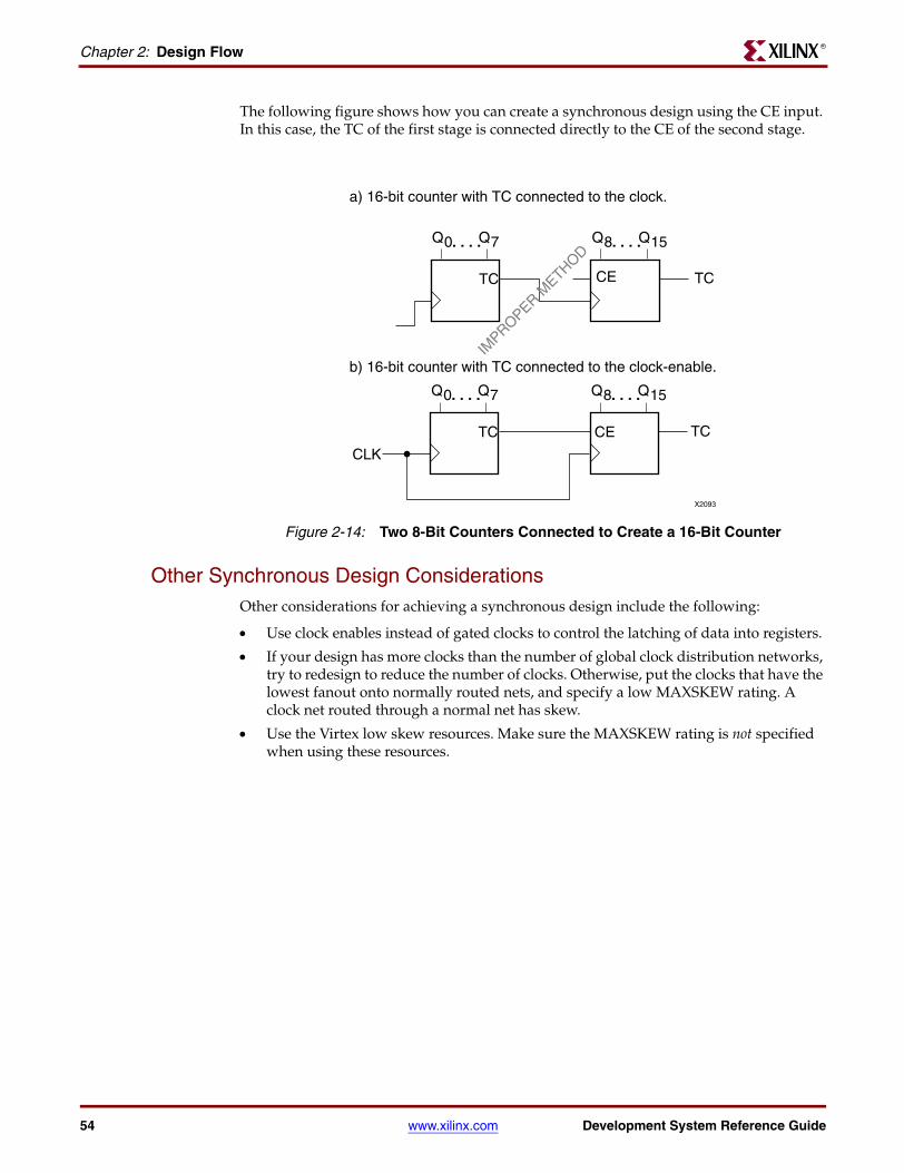
The following figure shows how you can create a synchronous design using the CE input. In this case, the TC of the first stage is connected directly to the CE of the second stage.
Other Synchronous Design ConsiderationsOther considerations for achieving a synchronous design include the following:
• Use clock enables instead of gated clocks to control the latching of data into registers.
• If your design has more clocks than the number of global clock distribution networks, try to redesign to reduce the number of clocks. Otherwise, put the clocks that have the lowest fanout onto normally routed nets, and specify a low MAXSKEW rating. A clock net routed through a normal net has skew.
• Use the Virtex low skew resources. Make sure the MAXSKEW rating is not specified when using these resources.
Figure 2-14: Two 8-Bit Counters Connected to Create a 16-Bit Counter
a) 16-bit counter with TC connected to the clock.
TC
Q0 Q7. . . .
TC
Q8 Q15. . . .
CE
X2093
TC
b) 16-bit counter with TC connected to the clock-enable.
Q0 Q7. . . .
TC
Q8 Q15. . . .
CE
CLK
IMPROPER M
ETHOD
54 www.xilinx.com Development System Reference Guide