DEVELOPMENT OF LIGHTWEIGHT AND LOW-COST ...
142
DEVELOPMENT OF LIGHTWEIGHT AND LOW-COST MICROWAVE COMPONENTS FOR REMOTE-SENSING APPLICATIONS A Dissertation Presented to The Academic Faculty By Carlos A. Donado Morcillo In Partial Fulfillment of the Requirements for the Degree Doctor of Philosophy in Electrical and Computer Engineering School of Electrical and Computer Engineering Georgia Institute of Technology May 2013 Copyright c 2013 by Carlos A. Donado Morcillo
-
Upload
khangminh22 -
Category
Documents
-
view
0 -
download
0
Transcript of DEVELOPMENT OF LIGHTWEIGHT AND LOW-COST ...
DEVELOPMENT OF LIGHTWEIGHT AND
LOW-COST MICROWAVE COMPONENTS FOR
REMOTE-SENSING APPLICATIONS
A Dissertation
Presented toThe Academic Faculty
By
Carlos A. Donado Morcillo
In Partial Fulfillment
of the Requirements for the DegreeDoctor of Philosophy
in
Electrical and Computer Engineering
School of Electrical and Computer EngineeringGeorgia Institute of Technology
May 2013
Copyright c! 2013 by Carlos A. Donado Morcillo

DEVELOPMENT OF LIGHTWEIGHT AND
LOW-COST MICROWAVE COMPONENTS FOR
REMOTE-SENSING APPLICATIONS
Approved by:
Dr. John Papapolymerou, AdvisorProfessor, School of ECE
Georgia Institute of Technology
Dr. Gregory Durgin
Professor, School of ECE
Georgia Institute of Technology
Dr. Andrew PetersonProfessor, School of ECE
Georgia Institute of Technology
Dr. Oliver BrandProfessor, School of ECE
Georgia Institute of Technology
Dr. Cli!ord Henderson
School of Chemical and Biomolecular Engi-
neering
Georgia Institute of Technology
Date Approved: 16 December 2012

To my mother Zenaida and to my family for the unconditional love and support.

ACKNOWLEDGMENTS
First and foremost, I would like to express my deepest gratitude to my advisor, Dr. John
Papapolymerou, for the enormous support he provided throughout my PhD studies at Geor-
gia Tech. The amount of freedom to pursue my ideas and remarkable opportunities he has
provisioned (and keeps facilitating) have surpassed all the professional expectations I used
to have as a young Panamanian engineer. His advise, which has gone beyond the technical
realm in many occasions, has helped me to mature as a person and as a researcher, and to
appreciate the value of hard work and dedication in academia.
I would like to acknowledge the inspirational influence of Dr. Orlando Concepcion,
from Universidad Catolica Santa Maria la Antigua (USMA) in Panama, and of Dr. Glenn
Smith, from Georgia Tech. Their teachings, character, wisdom and challenging classes fos-
tered and reinforced my fascination for electromagnetism and wireless technologies. I also
give a special recognition to my mentor Prof. Ing. Anselmo Araolaza and the personnel of
the National Centre of Metrology of Panama (CENAMEP) for instructing me in the art of
measurements, and for providing me with the necessary intuition and skills to confront the
toughest laboratory challenges throughout my PhD research.
I would like to thank my sponsors for financially supporting my research. I thank the
National Space Administration (NASA) for supporting my work on the development of
a lightweight-phased-arrays technology for the study of cold-land processes. Without a
doubt, this was the most challenging, interesting and exciting project I have undertaken in
my professional career. I would like to thank, besides the Mirctech members who were
involved, the multidisciplinary team that helped this project to become a real success. In
particular, I deeply value the contributions of Dr. John Cressler and his research group
members Christopher Coen and Dr. John Poh for the endless hours of dedication and lab
action. I would also like to thank Dr. Ted Heath and Bill Wilson from the Georgia Tech
Research Institute for making me feel as welcome as I could be in their hi-tech facilities.
iv
I thank Nanowave Technologies for funding the final projects of my research. Espe-
cially, I would like to acknowledge the constructive support of Dr. Justin Miller and Dr.
Huifang Gu in the development of the sponsored projects. I deeply appreciate the encour-
agement to pursue design creativity, which was at the same time greatly benefited with
their input. The interactions with them have been the first real exposure I have had with
industry in the RF field, and the experience so far has been indeed extremely valuable for
my professional formation.
I dearly appreciate the interactions with the incredible group of individuals, past and
current, that form the MircTech research group. Socially and technically, my journey was
enriching and fun all at once thanks to all my lab mates. I would like to acknowledge the
technical and grammatical support of Dr. Benjamin Lacroix, who took the time to carefully
proofread most of my papers before publication (thank you for being my No. 1 reader!).
I would like to thank Dr. Chad Patterson for his selfless support and collaboration during
the NASA project. It was an honor to work with him, learn from his technical expertise
and from his design techniques. I would like to thank the past members of the group Dr.
Swapan Bhattacharya, Dr. Arnaud Amadjikpe, Dr. David Chung, Dr. Stanis Courreges, Dr.
Yuan Li, Dr. Negar Tavassolian, Ana M. Yepes, and Diana D. Fuertes; to current members:
Aida Vera, Wasif Kahn, Fan Cai, Spyridon Pavlidis, Outmane Lemtiri (a.k.a. “Lemitri”)
and Chris Barisich for all the good times and stimulating political/ philosophical/ religious/
social/ technical conversations that constantly kept elevating the intellectual level of the
group, and improving each of us as well-rounded human beings.
I thank the Georgia Tech Surf Club members for all the surf trips and fun extracur-
ricular activities that helped me keep my sanity during stressful times. Also I would like
to acknowledge the support of the sta! and members of Panamanian Students at Georgia
Tech (PANAS@GT) for allowing me to keep connected to Panama and its culture through
multiple social activities. I would like to thank all the friends that have come and gone
here in Atlanta, especially, Dr. Matthew Lee-Crane and Dr. Alexander Epple for providing
v

a seamless and entertaining transition into graduate school. I would like to thank Jorge
Hernandez, Maribel Baker and Dr. Rolando Gittens for all the refreshing debates about
Panamanian social development and politics and for constant support throughout my life in
Atlanta.
I would like to give special thanks to my friends Mirielle Medina, Hilary Hughes, Fer-
nando Lopez, Peter Pusztai, Grimaldo Urena, Irma Law, Katherine Fong, Miguel M. Ser-
rano E., Charlotte Richardson and Carlos Montalvo for giving me support, encouragement
and company when it was mostly needed during these past years. I thank my family, in
particular, my sister Ana Maria Solis and her husband Efrain Corro for always being there
with their love and support. To my dear nephews Efrain F. Corro and Daniel A. Corro,
I thank you for not forgetting me and I hope all the tutoring will help you to understand,
perhaps some day, what is written in the following pages. I thank my father, Jose Manuel
Donado, for helping me take the right decisions that took me to where I am.
I am profoundly grateful to my mother Zenaida Morcillo for devoting a lifetime of
sacrifice in my education and upbringing. Her relentless and unconditional love, patience,
dedication and support gave me the courage to truly believe that “querer es poder”. Finally,
I would like to thank my beloved wife Dr. Zohre Kurt for encouraging me to thrive as a
researcher and for supporting me in countless ways in my life as a PhD student. Her self
discipline, hard work, and dependability are qualities that every day inspire and motivate
me to improve my work and to do my best in everything I do.
vi
TABLE OF CONTENTS
DEDICATION . . . . . . . . . . . . . . . . . . . . . . . . . . . . . . . . . . . . . iii
ACKNOWLEDGMENTS . . . . . . . . . . . . . . . . . . . . . . . . . . . . . . . iv
LIST OF TABLES . . . . . . . . . . . . . . . . . . . . . . . . . . . . . . . . . . . x
LIST OF FIGURES . . . . . . . . . . . . . . . . . . . . . . . . . . . . . . . . . . xi
LIST OF SYMBOLS, ABBREVIATIONS AND TERMS . . . . . . . . . . . . . xv
SUMMARY . . . . . . . . . . . . . . . . . . . . . . . . . . . . . . . . . . . . . . xx
CHAPTER 1 INTRODUCTION . . . . . . . . . . . . . . . . . . . . . . . . . . 11.1 Modern Applications of Radar Systems . . . . . . . . . . . . . . . . . . . 3
1.2 New Trends in Compact and Lightweight RF Front End Packaging . . . . 41.3 Implementation Challenges for Lightweight and Low-cost RF Front Ends . 8
1.3.1 Dielectric Material Characterization Challenges . . . . . . . . . . 81.3.2 Integration of Active Components in Organic Antenna Panels . . . 101.3.3 Increasing the E!ective Isotropically-Radiated Power and Ther-
mal Management in Lightweight Front Ends . . . . . . . . . . . . 111.4 Thesis Overview . . . . . . . . . . . . . . . . . . . . . . . . . . . . . . . 11
CHAPTER 2 CHARACTERIZATION OF LOW-COST AND LIGHTWEIGHT
RF SUBSTRATES . . . . . . . . . . . . . . . . . . . . . . . . . . 132.1 Introduction . . . . . . . . . . . . . . . . . . . . . . . . . . . . . . . . . 13
2.2 Experiment and Circuit Design . . . . . . . . . . . . . . . . . . . . . . . 152.3 The Relative Permittivity Model . . . . . . . . . . . . . . . . . . . . . . 192.4 The Loss Tangent Model . . . . . . . . . . . . . . . . . . . . . . . . . . 21
2.4.1 Total Loss Calculation . . . . . . . . . . . . . . . . . . . . . . . 222.4.2 Conductor Loss Calculation . . . . . . . . . . . . . . . . . . . . . 23
2.5 Circuits Fabrication and Experimental Setup . . . . . . . . . . . . . . . . 242.6 Monte Carlo Uncertainty Analysis and Matlab Code . . . . . . . . . . . . 262.7 Measurement Results . . . . . . . . . . . . . . . . . . . . . . . . . . . . 27
CHAPTER 3 A LIGHTWEIGHT, ORGANIC PHASED ARRAY WITH WIRE-BONDED ICS IN THE X BAND . . . . . . . . . . . . . . . . . . 30
3.1 Introduction . . . . . . . . . . . . . . . . . . . . . . . . . . . . . . . . . 30
3.2 System Overview . . . . . . . . . . . . . . . . . . . . . . . . . . . . . . 323.2.1 Substrate Stack-up . . . . . . . . . . . . . . . . . . . . . . . . . 33
3.2.2 Array Digital Control and Power Supply Module . . . . . . . . . 343.3 Design Procedure and Simulations . . . . . . . . . . . . . . . . . . . . . 353.4 Fabrication and Measurements . . . . . . . . . . . . . . . . . . . . . . . 35
vii

CHAPTER 4 DEVELOPMENT OF LOW-PROFILE INTERCONNECTS FORHIGHLY-INTEGRATED ORGANIC PHASED ARRAYS . . . . 40
4.1 Introduction . . . . . . . . . . . . . . . . . . . . . . . . . . . . . . . . . 40
4.2 Design Procedure . . . . . . . . . . . . . . . . . . . . . . . . . . . . . . 414.2.1 Stripline and Substrate Geometry . . . . . . . . . . . . . . . . . . 41
4.2.2 Via-Fences Design . . . . . . . . . . . . . . . . . . . . . . . . . 424.2.3 CPW-SL Transition . . . . . . . . . . . . . . . . . . . . . . . . . 44
4.3 Measurements . . . . . . . . . . . . . . . . . . . . . . . . . . . . . . . . 46
CHAPTER 5 AN ULTRA-THIN, HIGH-POWER, T/R ORGANIC ANTENNAARRAY WITH FLIP-CHIP BONDED INTEGRATED CIRCUITSIN THE X BAND . . . . . . . . . . . . . . . . . . . . . . . . . . 49
5.1 Introduction . . . . . . . . . . . . . . . . . . . . . . . . . . . . . . . . . 495.2 Array Design . . . . . . . . . . . . . . . . . . . . . . . . . . . . . . . . . 50
5.2.1 Substrate Stack Details . . . . . . . . . . . . . . . . . . . . . . . 515.2.2 Stripline BFN . . . . . . . . . . . . . . . . . . . . . . . . . . . . 525.2.3 SiGe TRIC Technology and Packaged Performance . . . . . . . . 54
5.2.4 Microstrip Patch Antennas . . . . . . . . . . . . . . . . . . . . . 575.3 Array Fabrication Process . . . . . . . . . . . . . . . . . . . . . . . . . . 59
5.3.1 Antenna Board Lamination . . . . . . . . . . . . . . . . . . . . . 60
5.3.2 TRIC Flip-Chip Bonding Procedure . . . . . . . . . . . . . . . . 615.4 Array Performance . . . . . . . . . . . . . . . . . . . . . . . . . . . . . . 62
5.4.1 Small-Signal Measurements . . . . . . . . . . . . . . . . . . . . 625.4.2 Large-Signal Measurements . . . . . . . . . . . . . . . . . . . . 655.4.3 Estimation of G/T . . . . . . . . . . . . . . . . . . . . . . . . . 68
5.4.4 Comparison With Other Works . . . . . . . . . . . . . . . . . . . 69
CHAPTER 6 THERMAL ASPECTS IN THE DESIGN OF LIGHTWEIGHT
RADAR FRONT-ENDS . . . . . . . . . . . . . . . . . . . . . . . 726.1 Introduction . . . . . . . . . . . . . . . . . . . . . . . . . . . . . . . . . 726.2 Analytical Assessment of the Power-Handling Capacity of Thin-Film Sub-
strates . . . . . . . . . . . . . . . . . . . . . . . . . . . . . . . . . . . . 736.2.1 Thermal Analysis Formulation . . . . . . . . . . . . . . . . . . . 736.2.2 Thermal Assessment Results . . . . . . . . . . . . . . . . . . . . 75
6.3 Thermal Characterization of the RF Properties of Rogers 6002 . . . . . . 786.3.1 Determination of the Normalized Temperature Coe"cients . . . . 79
6.3.2 Design and Fabrication of the Test Circuits . . . . . . . . . . . . . 806.3.3 Measurement Procedure . . . . . . . . . . . . . . . . . . . . . . . 806.3.4 Measurement Results . . . . . . . . . . . . . . . . . . . . . . . . 82
CHAPTER 7 COMPACT AND LOW-COST TOPOLOGY FOR EVANESCENT-MODE WAVEGUIDE FILTERS WITH DIELECTRIC LOAD-ING IN THE X BAND . . . . . . . . . . . . . . . . . . . . . . . . 88
7.1 Inctroduction . . . . . . . . . . . . . . . . . . . . . . . . . . . . . . . . . 887.2 A New FoM for Cavity Filters . . . . . . . . . . . . . . . . . . . . . . . 90
viii

7.3 Design Procedure . . . . . . . . . . . . . . . . . . . . . . . . . . . . . . 917.4 Fabricated Prototype and Measurements . . . . . . . . . . . . . . . . . . 95
CHAPTER 8 CONCLUSION . . . . . . . . . . . . . . . . . . . . . . . . . . . 99
8.1 List of Contributions . . . . . . . . . . . . . . . . . . . . . . . . . . . . . 1008.2 Future Work . . . . . . . . . . . . . . . . . . . . . . . . . . . . . . . . . 102
8.3 List of Publications and Academic Achievements . . . . . . . . . . . . . 1048.3.1 Awards . . . . . . . . . . . . . . . . . . . . . . . . . . . . . . . 1048.3.2 Invention Disclosures . . . . . . . . . . . . . . . . . . . . . . . . 104
8.3.3 Journal Articles . . . . . . . . . . . . . . . . . . . . . . . . . . . 1048.3.4 Conference Papers . . . . . . . . . . . . . . . . . . . . . . . . . 104
APPENDIX A DESIGN OF WILKINSON POWER DIVIDERS ON ALUMINUM
NITRIDE WITH TANTALUM NITRIDE RESISTORS . . . . . 106A.1 Design of an Equal-Split, Two-way WPD . . . . . . . . . . . . . . . . . . 107
A.2 Design of a Three-way WPD . . . . . . . . . . . . . . . . . . . . . . . . 108A.3 Design of a Four-way WPD . . . . . . . . . . . . . . . . . . . . . . . . . 110
REFERENCES . . . . . . . . . . . . . . . . . . . . . . . . . . . . . . . . . . . . . 112
VITA . . . . . . . . . . . . . . . . . . . . . . . . . . . . . . . . . . . . . . . . . . 122
ix
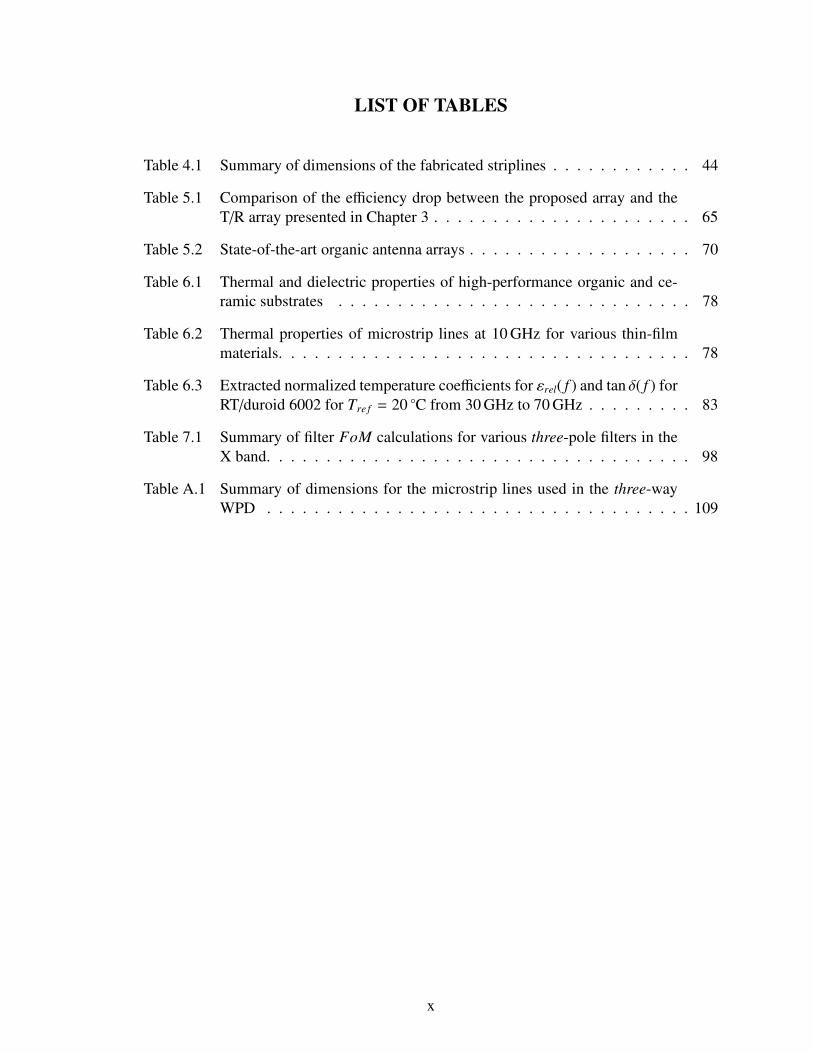
LIST OF TABLES
Table 4.1 Summary of dimensions of the fabricated striplines . . . . . . . . . . . . 44
Table 5.1 Comparison of the e"ciency drop between the proposed array and the
T/R array presented in Chapter 3 . . . . . . . . . . . . . . . . . . . . . . 65
Table 5.2 State-of-the-art organic antenna arrays . . . . . . . . . . . . . . . . . . . 70
Table 6.1 Thermal and dielectric properties of high-performance organic and ce-ramic substrates . . . . . . . . . . . . . . . . . . . . . . . . . . . . . . 78
Table 6.2 Thermal properties of microstrip lines at 10 GHz for various thin-film
materials. . . . . . . . . . . . . . . . . . . . . . . . . . . . . . . . . . . 78
Table 6.3 Extracted normalized temperature coe"cients for !rel( f ) and tan "( f ) for
RT/duroid 6002 for Tre f = 20 "C from 30 GHz to 70 GHz . . . . . . . . . 83
Table 7.1 Summary of filter FoM calculations for various three-pole filters in the
X band. . . . . . . . . . . . . . . . . . . . . . . . . . . . . . . . . . . . 98
Table A.1 Summary of dimensions for the microstrip lines used in the three-way
WPD . . . . . . . . . . . . . . . . . . . . . . . . . . . . . . . . . . . . 109
x
LIST OF FIGURES
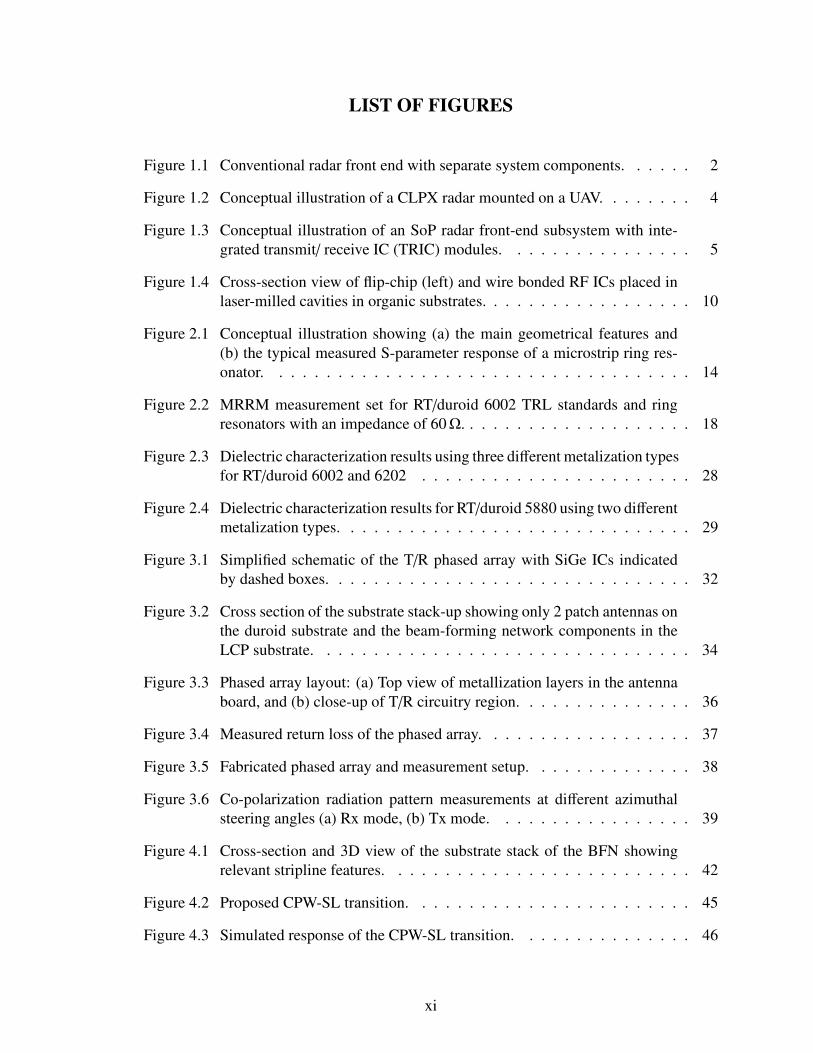
Figure 1.1 Conventional radar front end with separate system components. . . . . . 2
Figure 1.2 Conceptual illustration of a CLPX radar mounted on a UAV. . . . . . . . 4
Figure 1.3 Conceptual illustration of an SoP radar front-end subsystem with inte-grated transmit/ receive IC (TRIC) modules. . . . . . . . . . . . . . . . 5
Figure 1.4 Cross-section view of flip-chip (left) and wire bonded RF ICs placed inlaser-milled cavities in organic substrates. . . . . . . . . . . . . . . . . . 10
Figure 2.1 Conceptual illustration showing (a) the main geometrical features and
(b) the typical measured S-parameter response of a microstrip ring res-onator. . . . . . . . . . . . . . . . . . . . . . . . . . . . . . . . . . . . 14
Figure 2.2 MRRM measurement set for RT/duroid 6002 TRL standards and ringresonators with an impedance of 60#. . . . . . . . . . . . . . . . . . . . 18
Figure 2.3 Dielectric characterization results using three di!erent metalization typesfor RT/duroid 6002 and 6202 . . . . . . . . . . . . . . . . . . . . . . . 28
Figure 2.4 Dielectric characterization results for RT/duroid 5880 using two di!erentmetalization types. . . . . . . . . . . . . . . . . . . . . . . . . . . . . . 29
Figure 3.1 Simplified schematic of the T/R phased array with SiGe ICs indicatedby dashed boxes. . . . . . . . . . . . . . . . . . . . . . . . . . . . . . . 32
Figure 3.2 Cross section of the substrate stack-up showing only 2 patch antennas onthe duroid substrate and the beam-forming network components in the
LCP substrate. . . . . . . . . . . . . . . . . . . . . . . . . . . . . . . . 34
Figure 3.3 Phased array layout: (a) Top view of metallization layers in the antenna
board, and (b) close-up of T/R circuitry region. . . . . . . . . . . . . . . 36
Figure 3.4 Measured return loss of the phased array. . . . . . . . . . . . . . . . . . 37
Figure 3.5 Fabricated phased array and measurement setup. . . . . . . . . . . . . . 38
Figure 3.6 Co-polarization radiation pattern measurements at di!erent azimuthalsteering angles (a) Rx mode, (b) Tx mode. . . . . . . . . . . . . . . . . 39
Figure 4.1 Cross-section and 3D view of the substrate stack of the BFN showingrelevant stripline features. . . . . . . . . . . . . . . . . . . . . . . . . . 42
Figure 4.2 Proposed CPW-SL transition. . . . . . . . . . . . . . . . . . . . . . . . 45
Figure 4.3 Simulated response of the CPW-SL transition. . . . . . . . . . . . . . . 46
xi

Figure 4.4 Top View of two of the fabricated samples. . . . . . . . . . . . . . . . . 47
Figure 4.5 Measured S-Parameters of all striplines (TRL). . . . . . . . . . . . . . . 47
Figure 4.6 Measured S-Parameters of all samples with transitions (SOLT). . . . . . 48
Figure 5.1 Simplified schematic diagram of the proposed antenna array. . . . . . . . 50
Figure 5.2 Cross-section view of the array substrate stack showing the conceptual
distribution of components (the thickness of the metallization and sub-strate layers are shown in parentheses). . . . . . . . . . . . . . . . . . . 51
Figure 5.3 Multilayer top view of the stripline 3 dB splitter. . . . . . . . . . . . . . 53
Figure 5.4 Electromagnetic model of the stripline eight-way splitter and distributionof |E|2. . . . . . . . . . . . . . . . . . . . . . . . . . . . . . . . . . . . 54
Figure 5.5 Simulated S parameters of the stripline eight-way splitter. . . . . . . . . 54
Figure 5.6 Electromagnetic model of the stripline-to-CPW transition (duroid sub-
strate not shown). . . . . . . . . . . . . . . . . . . . . . . . . . . . . . . 55
Figure 5.7 Simulated S-parameters of the stripline-to-CPW transition. . . . . . . . . 55
Figure 5.8 Optional caption for list of figures . . . . . . . . . . . . . . . . . . . . . 55
Figure 5.9 Measured S-parameters of singly-packaged TRICs in Tx and Rx mode,with and without epoxy underfill. . . . . . . . . . . . . . . . . . . . . . 57
Figure 5.10 Average noise figure over frequency, extracted from measurements offive singly-packaged SiGe TRICs with epoxy underfill. . . . . . . . . . . 58
Figure 5.11 Output power and gain linearity measurements of a singly-packagedTRIC with epoxy underfill in Tx mode. . . . . . . . . . . . . . . . . . . 58
Figure 5.12 Multilayer top view of the feed layout for a pair of patch-antennas. . . . . 59
Figure 5.13 Top view of the TRIC Zone with photographs of the recessed cavity(upper right) and the mounted TRIC with epoxy underfill (lower right). . 61
Figure 5.14 Fabricated antenna array board and anechoic chamber setup. . . . . . . . 62
Figure 5.15 Measured and simulated S 11 of the proposed antenna array in Tx and Rx
modes. . . . . . . . . . . . . . . . . . . . . . . . . . . . . . . . . . . . 63
Figure 5.16 Estimated far-field radiation pattern based on near-field measurementsin the azimuthal direction. . . . . . . . . . . . . . . . . . . . . . . . . . 63
xii

Figure 5.17 Measured Tx and Rx broadside gain over frequency and comparisonwith the T/R phased array presented in Chapter 3 (Donado Morcillo etal. 2011). . . . . . . . . . . . . . . . . . . . . . . . . . . . . . . . . . . 64
Figure 5.18 Schematic diagram of EIRP measurement Configuration A and Config-uration B. . . . . . . . . . . . . . . . . . . . . . . . . . . . . . . . . . . 67
Figure 5.19 Measured EIRP with Configuration A and Configuration B for various
values of Pin. . . . . . . . . . . . . . . . . . . . . . . . . . . . . . . . . 68
Figure 5.20 Measured EIRP over frequency using Configuration A for Pin = 36.2 dBm. 68
Figure 6.1 APHC (Tamb = 25 "C, f = 10 GHz) for various geometries of 50# lineson LCP . . . . . . . . . . . . . . . . . . . . . . . . . . . . . . . . . . . 76
Figure 6.2 APHC (Tamb = 25 "C, f = 10 GHz) comparison of 50# transmissionlines between commercially-available geometries of di!erent dielectric
substrates. . . . . . . . . . . . . . . . . . . . . . . . . . . . . . . . . . . 77
Figure 6.3 (a) Measurement-setup cross section (b) probing and performance net-
work analyzer, and (c) detail of the area surrounding the sample. . . . . . 82
Figure 6.4 Temperature dependence of !rel( f , T ) of RT/duroid 6002 from 30 GHzto 70 GHz (70# resonator). . . . . . . . . . . . . . . . . . . . . . . . . 84
Figure 6.5 Temperature dependence of tan "( f , T ) of RT/duroid 6002 from 30 GHzto 70 GHz (70# resonator). . . . . . . . . . . . . . . . . . . . . . . . . 85
Figure 6.6 Temperature dependence of !rel( f , T ) of RT/duroid 6002 around 60 GHz(60# and 70# resonators). . . . . . . . . . . . . . . . . . . . . . . . . 85
Figure 6.7 Temperature dependence of tan "( f , T ) of RT/duroid 6002 around 60 GHz(60# and 70# resonators). . . . . . . . . . . . . . . . . . . . . . . . . 86
Figure 6.8 Thermal variation of the extracted !rel( f , T ) for RT/duroid 6002 from20 "C to 70 "C and from 30 GHz to 70 GHz (60# and 70# resonators). . 86
Figure 6.9 Thermal variation of the extracted tan "( f , T ) for RT/duroid 6002 from20 "C to 70 "C and from 30 GHz to 70 GHz (60# and 70# resonators). . 87
Figure 7.1 (a) Rectangular waveguide resonator and (b) proposed filter topologywith detached side walls (the walls are shown transparent for demon-
stration). . . . . . . . . . . . . . . . . . . . . . . . . . . . . . . . . . . 89
Figure 7.2 Illustration of the pre-specified volume dissected into three resonator
sections with equal volume and dimensions a, b and L. . . . . . . . . . . 92
Figure 7.3 Simulated e!ect of Wqtz over f0 and Qu of the T E10 evanescent mode ofa single-resonator. . . . . . . . . . . . . . . . . . . . . . . . . . . . . . 93
xiii

Figure 7.4 Simulated inter-resonator coupling study: (a) S 21 response for weak RFfeed coupling, (b) extracted coupling coe"cient relation to Liris, and (c)cross-section view of the electromagnetic model used. . . . . . . . . . . 94
Figure 7.5 Simulated group-delay (#S 11) response of a sinlgy-loaded resonator for
various values of Wqtz. . . . . . . . . . . . . . . . . . . . . . . . . . . . 95
Figure 7.6 Manufactured filter prototype . . . . . . . . . . . . . . . . . . . . . . . 96
Figure 7.7 Scattering-parameter response: simulation and measurement. . . . . . . 97
Figure 7.8 Simulated change in S 11 with I/O probe length variations within ±20 µmaround the optimal value. . . . . . . . . . . . . . . . . . . . . . . . . . . 97
Figure A.1 Schematic diagram of a two-way WPD with equal power split. . . . . . . 106
Figure A.2 Schematic diagram of a two-way WPD with unequal power split K. . . . 107
Figure A.3 Optimized electromagnetic model of the two-way WPD. . . . . . . . . . 108
Figure A.4 Simulated S-Parameters of the two-way WPD. . . . . . . . . . . . . . . 108
Figure A.5 Schematic diagram of the proposed three-way WPD. . . . . . . . . . . . 109
Figure A.6 Optimized electromagnetic model of the three-way WPD. . . . . . . . . 109
Figure A.7 Simulated S-Parameters of the three-way WPD. . . . . . . . . . . . . . . 110
Figure A.8 Optimized electromagnetic model of the four-way WPD. . . . . . . . . . 111
Figure A.9 Simulated S-Parameters of the four-way WPD. . . . . . . . . . . . . . . 111
xiv

LIST OF SYMBOLS, ABBREVIATIONS AND TERMS
$0 Signal propagation wavelength in vacuum in [m].
$g Signal wavelength in a wave-guiding structure in [m].
µ0 Premeability of vacuum: 4% # 10$7 H m$1.
tan "( f ) Loss tangent of a dielectric substrate at a given frequency f .
tan "( f , T ) Loss tangent of a dielectric substrate at a given frequency f
and temperature T .
tan " Loss tangent of a dielectric substrate. This nomenclature
refers to the loss tangent as a material characteristic, insteadof the value at a specific frequency or temperature.
!e f f E!ective permittivity of an electromagnetic-wave-guidingstructure.
!e f f (0) E!ective permittivity of a microstrip line calculated with a
quasi-static model.
!e f f ( f ) E!ective permittivity of a microstrip line calculated with a
frequency-dispersive model.
!rel( f ) Relative permittivity of a dielectric substrate at a given fre-quency f .
!rel( f , T ) Relative permittivity of a dielectric substrate at a given fre-quency f and temperature T .
!rel Relative permittivity of a dielectric substrate. This nomen-clature refers the relative permittivity as a material charac-teristic, instead of the value at a specific frequency or tem-
perature.
c0 Speed of light in vacuum: 299 792 458 m s$1.
EIRP E!ective isotropically-radiated power in [dBm].
f Frequency in Hz or multiples of Hz.
G/T “G” over “T” figure of merit for receive antenna systems, in
[dB].
IL Insertion loss in [dB].
xv
Ksub Thermal conductivity of a given “sub” dielectric substratein [W m$1 "C$1].
NF Noise figure in [dB].
PT x Transmit power in [dBm].
Rmax Radar range in [m].
RL Return loss in [dB].
T E Transverse electric (field/ mode)
T EM Transverse electromagnetic (field/ mode)
T M Transverse magnetic (field/ mode)
W Otherwise specified, this symbol refers to the microstrip sig-
nal width in [m].
Z0m Characteristic impedance of a microstrip line in [#].
3D Three dimensional.
1 mil 25.4 µm.
Al2O3 Aluminum Oxide (dielectric substrate, also known as alu-
mina).
AlN Aluminum nitride (ceramic dielectric substrate with !rel(10 GHz) =8.5 and tan "(10 GHz) = 0.003).
BW Bandwidth.
C band 4 GHz to 8 GHz.
CBCPW Conductor-backed coplanar waveguide.
CLPX Cold-land process (earth and atmospheric science).
CPW Coplanar waveguide.
Duroid RT/duroid R! 5880LZ (organic dielectric substrate with !rel(10 GHz) =1.96 and tan "(10 GHz) = 0.002).
ESA Electronically-steered array.
FPGA Field-programmable gate array.
I/O Input/ output.
IC Integrated circuit.
xvi

Ku band 12 GHz to 18 GHz.
L band 1 GHz to 2 GHz.
LCP Liquid crystal polymer (Organic dielectric substrate that,otherwise specified, corresponds to Rogers ULTRALAM
3850 with !rel(10 GHz) = 2.95 and tan "(10 GHz) = 0.0025).
LNA Low-noise amplifier.
MCUA Monte Carlo uncertainty analysis.
MEMS Micro-electromechanical system.
MRRM Microstrip Ring resonator method (for dielectric-substrate
characterization).
NASA National Space Administration.
PA Power amplifier.
PS Phase shifter.
PTFE Polytetrafluoroethylene (dielectric substrate, or simply Teflonby Dupont Company).
Radar Radio detection and ranging.
RF Radio frequency.
Rx Receive (refers to the receive functionality of a wireless sys-
tem).
S parameter Scattering parameter.
SIW Substrate integrated waveguide.
SoC System on chip (architecture for microwave circuits).
SOLT Short-open-load-thru (RF calibration algorithm).
SoP System on package (architecture for microwave/ electroniccircuits).
T/R Transmit/ receive (refers to the transmit/ receive functional-ity of a wireless system).
TaN Tantalum nitride (material used for thin-film resistors).
TRIC Transmit/ receive integrated circuit.
TRL Thru-reflect-line (RF calibration algorithm).
xvii

Tx Transmit (refers to the transmit functionality of a wirelesssystem).
UAV Unmanned aerial vehicle.
WPD Wilkinson power divider.
X band 8 GHz to 12 GHz.
xviii

Here is my secret. It is very simple: (...) what is essential is
invisible to the eye.
Le Petit Prince, Gallimard, 1943
Antoine de Saint Exupery
SUMMARY
The objective of the proposed research is to design, implement, and character-
ize low-cost, lightweight front-end components and subsystems in the microwave domain
through innovative packaging architectures for remote sensing applications. Particular em-
phasis is placed on system-on-package (SoP) solutions implemented in organic substrates
as a low-cost alternative to conventional, expensive, rigid, and fragile radio- frequency
(RF) substrates. To this end, the dielectric properties of organic substrates RT/duroid 5880,
6002 and 6202 are presented from 30 GHz to 70 GHz, covering most of the Ka and V radar
bands, giving also a thorough insight on the uncertainty of the microstrip ring resonator
method by means of the Monte Carlo uncertainty analysis.
Additionally, an ultra-thin, high-power antenna-array technology, with transmit/ receive
(T/R) functionality is introduced for mobile applications in the X band. Two lightweight
SoP T/R array panels are presented in this work using novel technologies such as Silicon
Germanium integrated circuits and microelectromechanical system switches on a hybrid
organic package of liquid crystal polymer and RT/duroid 5880LZ. A maximum power of
47 dBm is achieved in a package with a thickness of 1.8 mm without the need of bulky
thermal management devices.
Finally, to address the thermal limitations of thin-film substrates of interest (liquid crys-
tal polymer, RT/duroid 6002, alumina and Aluminum Nitride), a thermal assessment of mi-
crostrip structures is presented in the X band, along with the thermal characterization of the
dielectric properties of RT/duroid 6002 from 20 "C to 200 "C and from 30 GHz to 70 GHz.
Additional high-power, X-band technologies presented in this work include: a novel and
compact topology for evanescent mode filters, and low-profile Wilkinson power dividers
implemented on Aluminum Nitride using Tantalum Nitride thin-film resistors.
xx
CHAPTER 1
INTRODUCTION
With the confirmation of James Clerk Maxwell’s theory of electromagnetism by the exper-
imental physicist Heinrich Hertz, whereby Hertz demonstrated that electromagnetic waves
could reflect from remote objects [1], the notion of electromagnetic remote sensing be-
came widespread in many fields of modern society. The concept eventually evolved into
the radio detection and ranging (radar) technology, and has had a tremendous impact in
the development of accurate weather forecasting, aerial and terrestrial tra"c control, space
exploration, robotics, medical imaging, collision-avoidance systems, just to mention some
applications in addition to the traditional defense tactical systems.
Today, radar frequencies span the entire microwave spectrum [2], and the design of
radar radio-frequency (RF) circuitry has become a challenging task from integration and
performance perspectives. In particular, the design of RF front ends1.1 is the subject of
much research and innovation since it determines, among other parameters, the maximum
distance at which an object can be detected by the radar system (Rmax), defined by the
simplified form of the radar range equation [1]:
Rmax =
!PtGT xGRx$
20&
(4%)3S min
"1/4
, (1.1)
where Pt is the transmit power at the; GT x and GRx are the gains of the antenna system in
transmit (Tx) and receive (Rx) modes, respectively; $0 is the free-space wavelength of the
signal at the transmission frequency; & is the radar cross section, which “determines the
power density returned to the radar for a particular power density incident on the target”
[1]; and S min, the minimum power level that detectable by the Rx subsystem of the radar.
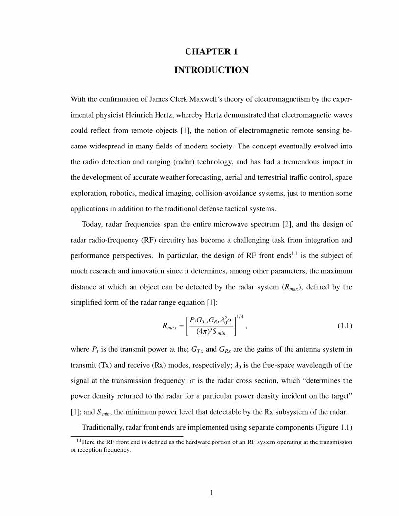
Traditionally, radar front ends are implemented using separate components (Figure 1.1)
1.1Here the RF front end is defined as the hardware portion of an RF system operating at the transmissionor reception frequency.
1

that include bulky waveguide sections and heavy antennas with parabolic reflectors be-
cause of their low-loss and high-power-handling characteristics. These advantageous prop-
erties allow the emission of a large Pt, which consequently increases Rmax. However, the
large-sized components represent a major limitation when the radar system has to be im-
plemented on a vehicle with space constraints such as an airplane, satellite or automobile.
Figure 1.1. Conventional radar front end with separate system components.
The system shown in Figure 1.1 corresponds to a monostatic radar, whereby the receiver
and transmitter modules are collocated and generally share the same antenna system. This
configuration, which is preferable for mobile applications because it minimizes the num-
ber of components, traditionally include a transmit/ receive (T/R) device that allows the
toggled or simultaneous operation of the system in Tx and Rx modes. The T/R device is
generally implemented through a circulator, single-pole double throw switch, duplexer or
any other device that can provide isolation between the Tx and Rx paths. In some cases, it
is also desired that electromagnetic energy is focused in di!erent directions by steering the
parabolic dish with an electromechanical system such as synchronous motor, which adds
functionality to the system at the cost of increasing its the bulk size and number of required
components.
An alternative to the conventional approach of motor-driven antenna beam-steering is
given by electronically steered arrays (ESA) of antennas, also known as phased arrays.
These antenna systems can achieve the same functionality occupying less space by steering
the main beam of the antenna through the variation of the phase of the current at each
2
radiating element [1]. Thus, a desirable characteristic in a lightweight, monostatic, radar
front end is high-performance electronic beam steering to eliminate the need for bulky
servo systems.
1.1 Modern Applications of Radar Systems
The advent of broadband wireless communications, high performance computing and inte-
grated circuit technologies in the latter part of the last century has allowed the implementa-
tion of mobile systems with powerful processing capabilities. Going beyond the scenarios
where signal processing is performed by high-end base stations, these developments have
enabled schemes where the radar measurement can be captured by a mobile unit and ana-
lyzed by the base station, or can be all performed in the autonomously-guided mobile units
at no loss of measurement quality.
An interesting example of a modern radar application is given by automotive radar
systems, which require compact solutions that can be seamlessly integrated in the vehicle
without significantly altering the appearance of the latter. In automobiles, a radar can be
used as a collision avoidance system or as a support device for adaptive automatic cruise
control. The frequencies used in automotive radar are diverse, but the ones for systems
deployed in the vehicles are generally high at 24 GHz, 77 GHz and 80 GHz [3]. Thus,
the corresponding millimeter-long wavelengths naturally reduce the size of the required
front-end circuitry, facilitating its integration in the vehicle.
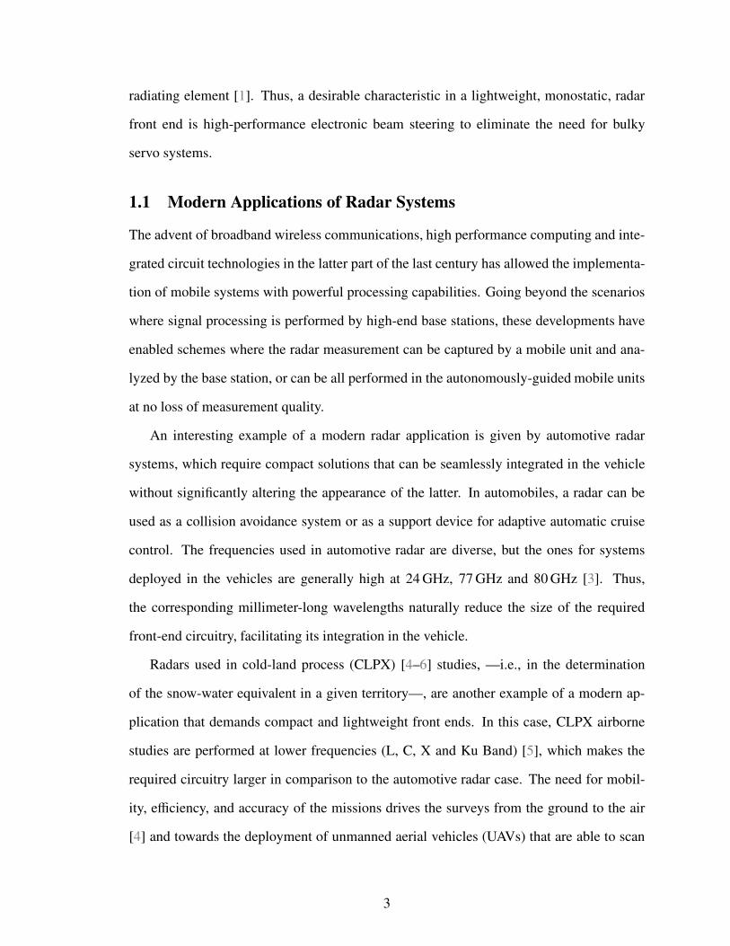
Radars used in cold-land process (CLPX) [4–6] studies, —i.e., in the determination
of the snow-water equivalent in a given territory—, are another example of a modern ap-
plication that demands compact and lightweight front ends. In this case, CLPX airborne
studies are performed at lower frequencies (L, C, X and Ku Band) [5], which makes the
required circuitry larger in comparison to the automotive radar case. The need for mobil-
ity, e"ciency, and accuracy of the missions drives the surveys from the ground to the air
[4] and towards the deployment of unmanned aerial vehicles (UAVs) that are able to scan
3
large amounts of terrain in a more expedite manner than in conventional ground missions
(Figure 1.2). Likewise, the space constraint in the UAVs motivates the development of
compact and lightweight electronic equipment for control and sensing. In particular, the
development of compact RF front ends that can be conformed to the outer chassis of the
UAVs is necessary to minimize real estate in the aircraft and to minimize its impact on the
UAV’s aerodynamics.
Figure 1.2. Conceptual illustration of a CLPX radar mounted on a UAV.
1.2 New Trends in Compact and Lightweight RF Front End Packag-
ing
The CLPX radar is one of the possible modern applications of radar technology whereby
conventional packaging techniques (i.e., circuits implemented on bulky waveguides or rigid
substrates) are not suitable for the realization of thin packages that could be conformed to
arbitrary surfaces. An attractive alternative to rigid RF architectures has arisen in recent
years with the emergence of organic substrates [7] that, besides having a lower cost than
conventional RF substrates, have the flexibility associated with polymeric materials and
stable dielectric characteristics at high frequencies.
Rogers ULTRALAM 3850, which is also known as liquid crystal polymer and referred
4

to in this work as LCP (!rel(10 GHz) = 2.95, tan "(10 GHz) = 0.0025) [8], is an example
of an organic substrate with high-performance RF properties [9]. LCP is one of the few
commercially available organic materials that has near-hermetic properties and that is ther-
mally matched to copper, and that has been extensively used in the implementation of RF
packages from a few GHz [10, 11] up to mm-wave frequencies [12–14].
Indeed, the available literature has shown that LCP is suitable for vertical integration
through multilayer schemes [15,16], embeddable circuits [17–19], and multi-substrate pla-
nar antenna arrays. For the latter instance, LCP has been successfully integrated in active
antenna panels [20, 21] with the organic substrate RT/duroidR! 5880LZ, which is referred
throughout this work as the “duroid” substrate (!rel(10 GHz) = 1.96, tan "(10 GHz) =
0.002) [8].
Recent developments in antenna arrays [21–28] have demonstrated the use of organic
substrates as a suitable solution for System-on-a-Package (SoP), wireless front ends. In an
SoP front end, the elements that provide Tx, Rx or T/R functionality are integrated directly
on the package that contains the radiating elements as shown in the conceptual illustration
of Figure 1.3.
Figure 1.3. Conceptual illustration of an SoP radar front-end subsystem with integrated transmit/receive IC (TRIC) modules.
SoP antenna boards must incorporate components crucial to the performance of the RF
front end such as power amplifiers (PA), low-noise amplifiers (LNA), T/R switches and
5

phase shifters (PS) to improve system parameters such as the noise figure (NF), the figure
of merit G/T [29], and the e!ective isotropically radiated power (EIRP). Here, EIRP
defined as the power radiated by the array system in the maximum gain direction of the
main beam:
EIRP = Pin + DA + 'A (dBm), (1.2)
where Pin is the input power at the RF feed of the transmit-antenna system, DA is the
antenna directivity and 'A is the e"ciency of the antenna beam-former network (BFN).
The need for a high EIRP is then justified clearly by rewriting 1.1 as follows:
Rmax =
!EIRP GRx $
20 &
(4%)3S min
"1/4
, (1.3)
which shows that the EIRP is a key factor in in maximizing Rmax.
Regarding Rx-only, SoP, organic antenna arrays, the available literature shows several
examples with multiple combinations of organic substrates and active technologies. For
instance, the X-band phased-array proposed in [20] uses two organic substrates (RT/duroid
5880LZ and LCP) and two silicon-germanium (SiGe) chips, each with an integrated LNA
and phase shifter. The four-bit phase shifters allow a discrete steering of the main beam of
±41" and a broadside gain of 40.1 dBi, in an array of 8 # 2 microstrip patch antennas.
An additional example is presented in [25], where an Rx-only phased array uses a single
silicon chip that drives eight planar dipoles in a teflon substrate. Just as in [20], the silicon
chips are wire bonded to the organic package. The array operates in the Ku Band, has
a beam-steering capability of approximately ±60" and has a peak receive gain of 40 dBi.
The gain is close to the one achieved in [20] with less elements, due to the fact that the
signal from each radiating element is combined actively in the silicon chip, which includes
a quadrature all-pass filter, two phase shifters and a current summer for each of the eight
RF channels.
In terms of Tx-only arrays, some recent implementations in organic substrates are also
6
found throughout published literature. The most remarkable one found in this literature sur-
vey was the one presented by Valdes-Garcia et al. [24], which shows a high EIRP in a com-
pact package, because the short wavelength of the operating frequency band (58.32 GHz-
64.8 GHz) allows a System-on-Chip (SoC) implementation. The SiGe active circuitry is
integrated on a BGA package that hosts 16 radiating elements. The chip occupies a total
area of 2.8 cm # 2.8 cm and is capable of achieving an EIRP of 40 dBm. The total DC
power consumption (which includes up-conversion, synthesizer, digital control and modu-
lator circuitry) is up to 6.5 W when transmitting at 64.8 GHz.
Another Tx-only example is presented in [23] where high-power unit cells are tiled to
form an array at 3.3 GHz, which achieves an EIRP of about 44 dBm per cell in an approach
that uses gallium nitride (GaN) ICs packaged on the organic substrate Rogers 4350BTM.
While a high EIRP per unit cell is demonstrated in this work, no multi-cell array operation
is shown; and bulky components, thick copper plates and ventilation mechanisms are used
to improve the power added e"ciency (PAE) of the GaN ICs, resulting in a rigid and high-
profile antenna panel.
Although the prototypes developed in these works demonstrate the capability of or-
ganic materials for state-of-the-art realizations of Rx- or Tx-only phased arrays, radar front-
ends should implement T/R functionality with a minimal number of components to achieve
maximum integration. An instance of an organic T/R prototype is found in the membrane
phased array demonstrated at 1.26 GHz in [22] designed for global earthquake observations
from satellites. In this array, gallium arsenide (GaAs) ICs are mounted on a PyraluxR! APTM
substrate with a 50 µm thickness. The long operational wavelength and real-estate require-
ment pushes a system-on-package (SoP) implementation, where the package size is about
112 cm # 60 cm, with eight GaAs modules integrated onto the board.
Finally, optimized for a communications application, the prototype presented in [30] is
another example of a T/R front end at a high frequency (60 GHz). Again, GaAs chips were
wire bonded to the organic package implemented on LCP. The array achieved an active Rx
7
gain of 31.8 dB and Tx gain of 21.6 dB, with a gain variation from 55 GHz to 63 GHz of
1 dB in Rx mode and of 3 dB in Tx.
1.3 Implementation Challenges for Lightweight and Low-cost RF Front
Ends
Although organic substrates might o!er many advantages in terms of cost and substrate
flexibility, there are several issues that must be resolved for their successful commercial
deployment. To enumerate some, these challenges include:
1. the accurate and broadband characterization of the dielectric properties of candidate
substrate materials for lightweight and flexible packaging,
2. the integration of active components in large antenna panels, and
3. the maximization of EIRP while minimizing the volume occupied by potential thermal-
management solutions.
1.3.1 Dielectric Material Characterization Challenges
The RF characterization of dielectric substrates, i.e., the determination of relative permittiv-
ity (!rel) and loss tangent (tan ", also known as the dissipation factor), plays a crucial role in
the development of microwave devices over a broad range of frequencies, not only for radar
applications, but also for modern high-speed communication systems that are emerging at
millimeter-wave frequencies. The drop in !rel and the increase in tan " is a well-documented
phenomenon for several dielectric materials as operating frequencies move from a few MHz
into and beyond the GHz spectrum. If a given material is not properly characterized and its
properties change drastically over frequency, the resulting inaccuracies in the calculation
of circuit parameters can either significantly prolong or just render impossible the design
and implementation of microwave systems.
Besides understanding the frequency dependence of !rel and tan ", it is also important
to understand the associated measurement uncertainty of these parameters. The importance
8
of a proper assessment of the !rel measurement uncertainty can be illustrated by calculating
the fundamental resonance frequency of a quarter-wavelength resonator at di!erent radar
frequencies. For this exercise, it is assumed that an LCP substrate is used with a thickness
of 4 mil, an 18 µm metallization thickness and an !rel = 2.95 ± 0.15, i.e., a 5 % expanded
uncertainty [31].
Quick calculations using [32], show that the impedance variation corresponding to the
relative permittivity uncertainty ranges 48.97# from to 51.10#, and that the resonant fre-
quency deviates ±0.21 GHz (±2.1 %) at 10 GHz. At at 70 GHz, the resonant frequency
varies about ±1.6 GHz (about 2.1 % as well) and the impedance, by ±1.0#. This example
shows, that although there is little variation in the impedance at both frequencies, the res-
onance frequency shift at 70 GHz is more severe. The shift in center frequency could be
tolerable for an antenna design, but for a narrow-band filter, the variation could severely
a!ect the implementation process.
Several methods for RF characterization have been proposed to this date [33] and gener-
ally involve either a microwave resonator circuit or a transmission line with a known prop-
agation model. Regarding resonator-based methods, the microstrip ring resonator method
(MRRM) [15, 34–36] has proven its reliability in the estimation of the RF characteriza-
tion of dielectrics, based on the recurrent resonances of the ring’s S 21 frequency response.
Besides the MRRM, other printed-circuit characterization techniques have been proposed
such as the T-resonator method [37]. The T-resonator method has an interesting advantage
over the MRRM since it actually has closed-form expressions for the radiation loss for
the open-end and tee-junction features of the resonator. However, microstrip-based char-
acterization methods are only as accurate as the equations used to model the microstrip.
Because most of the closed-form models where developed during and before 1980’s, when
sub-millimeter wave communication systems were topics of a distant future, the models
were a good fit up to only a few GHz [38]. Thus, a conscientious investigation of possible
sources of systematic errors as well as a proper assessment of measurement uncertainty of
9

planar methods is necessary at mm-wave frequenies.
1.3.2 Integration of Active Components in Organic Antenna Panels
With regards to mounting ICs on flexible organic packages, an aspect that needs to be inves-
tigated is the mechanical robustness and performance of chips packaged in fully integrated
systems or sub-systems such as T/R phased arrays. Although the wire bonded approach
[39] has been demonstrated a broad range of microwave frequencies [16, 17, 20, 30], RF
ICs flip-chip bonded to organic packages [17] also represent a promising technology for
SoP architectures. In a flip-chip bonded scheme (Figure 1.4), the IC is directly attached to
the package through solder joints.
Figure 1.4. Cross-section view of flip-chip (left) and wire bonded RF ICs placed in laser-milled cavitiesin organic substrates.
The flip-chip bonded approach can potentially improve the performance of the pack-
aged device by reducing the parasitic inductance otherwise added by long wire bonds.
Moreover, flip-chip bonding the ICs to the organic package can also expedite manufactur-
ing processes through high-speed automation, which inherently reduce assembly cost and
di"culty. Although these features may make the flip-chip bonded approach the preferred
method for packaging ICs in organic packages, this approach in many occasions requires
that additional support is provided to the chips by underfill materials [40, 41] that may add
an extra layer of di"culty in the RF package design.
The underfill material minimizes the mechanical stress caused by the thermal mismatch
10

between the chip substrate (glass or ceramic) and the package substrate (organic), reduc-
ing the possibility of solder-joint rupture, and hence improves the reliability of the pack-
age. However, the underfill material could interact with the layout circuitry of the chip
potentially degrading its performance at microwave frequencies, a pending issue that also
requires proper investigation.
1.3.3 Increasing the E!ective Isotropically-Radiated Power and Thermal Manage-
ment in Lightweight Front Ends
In spite of their high-performance characteristics, organic substrates face major packaging
challenges when the target of an organic array is to maximize EIRP. From an RF IC per-
spective, high-power amplifiers generally operate at high temperatures and require proper
thermal management. Depending on the RF IC technology chosen, thermal management
will in most cases consist of a thick and bulky metallic heat sink or ventilation system,
which inevitably imposes constraints on the package real estate and, hence, on the level of
integration of the array. From a substrate perspective, organic materials are poor thermal
conductors, which limits the amount of heat dissipated by the substrate. Altogether, these
packaging challenges must be resolved to implement high-power, RF front ends that can
take advantage of the lightweight and flexibility of organic substrates.
1.4 Thesis Overview
Several objectives are targeted in this thesis. An assessment of the uncertainty of the mi-
crostrip ring resonator method along with the dielectric properties of various thin-film,
organic materials is presented in Chapter 2 from 30 GHz to 70 GHz. In addition, the sys-
tematic error caused by the conductor-surface roughness on the measurement of the loss
tangent is characterized as well in Chapter 2.
An organic, ultra-low profile and lightweight T/R antenna array technology suitable for
X-band radars was developed for the CLPX program at NASA1.1[42], and is presented in
1.1National Space Administration
11
Chapter 3, Chapter 4 and Chapter 5. In Chapter 3, an organic phased array with wire-
bonded active devices is fully characterized. In Chapter 4 and Chapter 5 a novel packaging
architecture is introduced for the development of an ultra-thin and high-power organic T/R
array with flip-chip bonded SiGe ICs.
To answer questions about high power and high-temperature operation a thermal study
is performed for various thin-film materials in Chapter 6. The study includes analyzing
the average power-handling capacity of microstrip lines implemented on the substrates of
interest, and characterizing the thermal stability of the dielectric properties of RT/duroid
6002.
Finally, a novel, compact and low-cost filter topology is presented in Chapter 7 for a
high-power X-band radar application. The topology was developed for a robust operation
and for a reduced manufacturing complexity using a wire electric-discharge machining.
Compact size is achieved by using an evanescent-mode scheme with quartz dielectric load-
ing.
12

CHAPTER 2
CHARACTERIZATION OF LOW-COST AND LIGHTWEIGHT RF
SUBSTRATES
I often say that when you can measure what you are speaking
about, and express it in numbers, you know something about it;
but when you cannot express it in numbers, your knowledge is
of a meagre and unsatisfactory kind (...)
Lecture on ‘Electrical Units of Measurement’ (May 3, 1883),
Popular Lectures Vol. I, p. 73
SirWilliam Thompson (Lord Kelvin)
2.1 Introduction
The microstrip ring resonator method (MRRM) [9, 34–37, 43, 44] is a popular method for
the broadband extraction of the dielectric properties of materials used in planar microwave
circuits. Based on the multiple resonances observed in the S 21 response of these structures
and the physical dimensions of each resonator, the extraction of the !rel and the tan " is
achieved by solving the e!ective permittivity, impedance and loss models of the microstrip
structure.
The typical circuit layout of the microstrip ring resonator and the S 21 response with
the resonance peaks are shown in Figure 1(a) and Figure 1(b), respectively. The dielectric
properties of the materials are determined at the frequencies of these resonance peaks.
Although the estimation of !rel is in most cases a straightforward procedure in the
MRRM, the estimation of the loss tangent is still a challenging task for low-loss mate-
rials as noted in [15] for a number of reasons. First, the determination of the loss tangent is
an indirect measurement that depends in the correct calculation of the conductor loss and
the total loss of the material, assuming that the radiation loss is negligible under certain
13

(a)
(b)
Figure 2.1. Conceptual illustration showing (a) the main geometrical features and (b) the typical mea-sured S-parameter response of a microstrip ring resonator.
geometrical conditions of the ring [45]. Second, in a low-loss substrate, the conductor loss
is large in comparison with the dielectric loss and the value of the latter becomes extremely
sensitive to any overestimation of the parameters used to calculate the conductor loss, such
as the root-mean-square, conductor surface roughness ($rms) or the 3 dB bandwidth of the
peaks observed in the ring resonator frequency response.
Performing an in-depth experimental analysis of the e!ect of the e!ect of the $rms on
14

the extraction of the loss tangent, RF characterization results of several low-loss organic
substrates are reported. The study presented in this chapter, introduced originally in [46],
has two specific objectives:
1. to extract the relative permittivity (!rel) and the loss tangent (tan ") from 30 GHz
to 70 GHz of three low-loss, organic dielectric substrates: RT/duroidR! 5880, 6002,
6202 and, with nominal values at 10 GHz of !rel = [2.20, 2.94, 2.94], and tan " =
[0.0009, 0.0012, 0.0015], respectively; and
2. to experimentally investigate the e!ect of the $rms in the measurement of these quan-
tities using the MRRM.
In addition to fulfilling the above objectives, the content presented in this chapter is rele-
vant because it tests the classical, closed-form models developed used in MRRM dielectric
characterization for a high-frequency bandwidth (30 GHz to 70 GHz), for low-dielectric-
loss substrates and under di!erent levels of conductor surface roughness relative to the
skin depth ("s) [47] of the microwave signals. A systematic approach to the estimation
of the measurement uncertainty of the MRRM using the Monte Carlo Uncertainty Anal-
ysis (MCUA) [48] is also applied for the first time for the metrological assessment of the
method.
Three 1/2 oz copper sheets with di!erent $rms values were used to analyze the e!ect
of the $rms on the measurement of the tan ". The copper sheets correspond to a rolled
metallization with $rms = 0.2 µm (R), an electro-deposited metallization with $rms = 2 µm
(ED2), and an electro-deposited metallization with $rms = 3 µm (ED3).
2.2 Experiment and Circuit Design
For each of the three substrates, two sizes of microstrip ring resonators were designed at
three di!erent line impedances. Resonators at di!erent line impedances are desired because
they provide variations in the geometry of the designs, which allow to detect anomalous
15

results due to fabrication errors, and hence, validate the extracted dielectric properties of
the materials. Following the procedure described in [9], the dimensions of line impedances
of 60#, 70# and 90# were obtained with [32], using the relative permittivity and loss
tangent values provided by the manufacturer at 10 GHz.
Two main considerations were taken into account when designing the microstrip ring
resonators, whose main features are Figure 1(a). The first consideration involves the pro-
portion of the microstrip width (W) to the mean radius (rm) of each resonator. This pro-
portion was kept to below 0.2, i.e., W/rm % 0.2. Respecting this design rule is crucial
for resonators used in dielectric characterization: on the one hand, to avoid the excitation
of undesired resonant modes [45] that would otherwise lead to the erroneous extraction of
the dielectric properties of the substrate; and on the other hand, to reduce the radiation of
electromagnetic energy of the resonator to negligible levels. This last implication plays a
fundamental role in the validity of the model used in the extraction of the loss tangent of
the substrates.
The second design consideration deals with the mean radius of the ring resonator rm
and the desired number of resonant frequencies over the measurement bandwidth. As first
proposed in [43], by adjusting the mean radius of the resonator it is possible to tune its
fundamental frequency and the subsequent harmonics as follows:
2%rm = n$g (2.1)
where n is the harmonic corresponding to the integer multiple of the fundamental guided
wavelength ($g at n = 1). In terms of frequency, the above expression yields to the com-
monly used expression [9]:
fnth =n c
2 % rm
#!e f f ( f )
(2.2)
where fnth is the resonant frequency of the ring resonator, c is the speed of light in vacuum
and !e f f ( f ) is the frequency-dependent e!ective permittivity of the microstrip line. For the
16
design of the test structures, the !e f f ( f ) was calculated in [32] using the RF properties of
the substrate declared by the manufacturer at 10 GHz. Two ring resonators with di!erent
rm were designed for each of the three line impedance values, for each metalization type,
and for each of the three dielectric substrates. The rm of the larger resonator was adjusted
to provide between 5 to 6 resonances over the 30 GHz to 70 GHz bandwidth, and the rm of
the smaller resonator, 4 to 5 resonances (Figure 1(b)).
The feed of the resonators consisted of via-less, conductor-backed-coplanar waveguide
(CBCPW) to microstrip transitions, and were designed according to the guidelines pro-
vided in [49]. The end-to-end width of the CBCPW finite ground plane and the gap of
the CBCPW lines, was designed to allow the landing of probes with pitches of 250 µm
and 150 µm. The microstrip end of the transition is capacitively coupled to the resonator
through coupling gaps. The length of the gap was determined in simulation using [50] for
each dielectric material/ line impedance combination, so that the magnitude of the reso-
nances observed in the simulated S 21 response was below $20 dB2.1. This guarantees a
weak coupling to the resonator and prevents undesired shifts in the resonant frequencies
due to the source/load coupling, e!ect briefly described in [34].
A final simulation can be performed in [51] to analyze the radiation behavior of the
ring and to ensure that most of the radiation loss comes from the coupling gap. This last
simulation can be broken into two models. First, a back-to-back piece of microstrip line
can be interrupted in the middle by a gap of the same length than the one used for the
resonators. Second, the resonator structure can be simulated (using a symmetry plane for
instance) with the same microstrip lines used in the first step. Finally, far field simulations
performed at each resonance frequency of the ring can show the comparison between the
radiated power of both structures. If the radiation in the ring is minimal, both figures should
be close to each other.
Finally, a multi-line thru-reflect-line (TRL) calibration [52] set was designed for each
2.1Although an S 21 level of $20 dB is a conventionally accepted level for a weak coupling, from the argu-ments presented in [34] regarding the gap design, the designer should aim for levels below $30 dB.
17
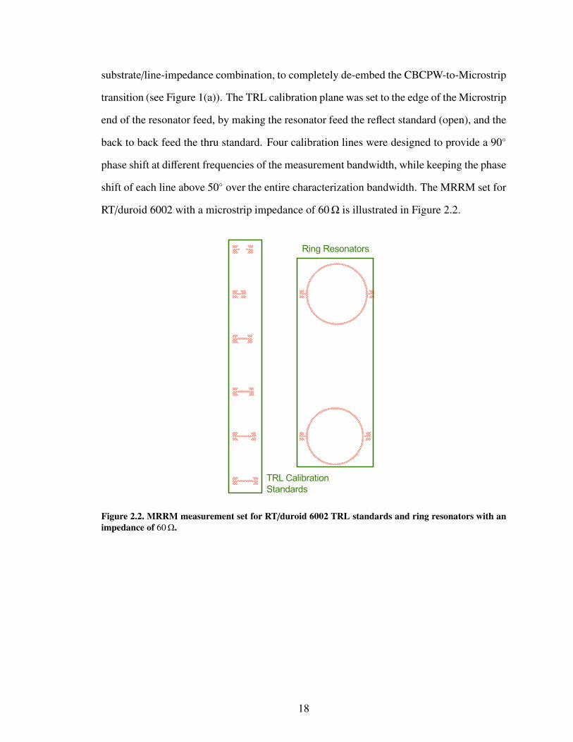
substrate/line-impedance combination, to completely de-embed the CBCPW-to-Microstrip
transition (see Figure 1(a)). The TRL calibration plane was set to the edge of the Microstrip
end of the resonator feed, by making the resonator feed the reflect standard (open), and the
back to back feed the thru standard. Four calibration lines were designed to provide a 90"
phase shift at di!erent frequencies of the measurement bandwidth, while keeping the phase
shift of each line above 50" over the entire characterization bandwidth. The MRRM set for
RT/duroid 6002 with a microstrip impedance of 60# is illustrated in Figure 2.2.
Figure 2.2. MRRM measurement set for RT/duroid 6002 TRL standards and ring resonators with animpedance of 60#.
18

2.3 The Relative Permittivity Model
The e!ective permittivity value of the microstrip line used in the ring resonator can be
extracted at each resonance solving for !e f f ( f ) in (2.2). Then, the frequency-dependent
relative permittivity, !rel( f ), can be extracted at each resonance (for f = fnth) from quasi-
static [53–56] or frequency-dispersive [57, 58] models of e!ective permittivity. For this
study, the model presented in [56] is chosen because it includes the e!ect of the microstrip
conductor thickness (t). Using this model, the value of the quasi-static e!ective permittivity
(!e f f (0)) is obtained as:
!e f f (0) =$%%%%%%%%%%%%&%%%%%%%%%%%%'
!rel( f ) + 1
2+!rel( f ) $ 1
2
())))*+1 +
12
W/h
,$1/2
+ 0.04-1 $
W
h
.2/00001 $ C, for W/h & 1
!rel( f ) + 1
2+!rel( f ) $ 1
2(1 + 12h/W)$1/2 $C, for W/h ' 1,
(2.3)
with
C =!rel( f ) $ 1
4.6
t/h(
W/h.
Solving for !rel( f ), (2.3) can be rewritten as:
!rel( f ) =2!e f f (0) + Mt $ 1
Mt + 1(2.4)
where the Mt represents the term that accounts for the e!ect of the metallization thickness,
and was defined in [46] as:
Mt = F(W/h) $2 · t/h
4.6(
W/h, (2.5)
where
F(W/h) =
$%%%%%%%%%%%&%%%%%%%%%%%'
(1 + 12h/W)$1/2 + 0.04 (1 $W/h)2 , for W/h & 1
(1 + 12h/W)$1/2 , for W/h ' 1.
(2.6)
19

The above quasi-static model can give a fair estimate of the !rel( f ) when !e f f (0) is
substituted by the !e f f ( f ) extracted from (2.2). This was the method adopted in [46]. Non-
tehteless, given that the electromagnetic energy does not propagate as a pure transverse
electromagnetic (T EM) mode in a microstrip line, the e!ect of frequency dispersion must
be considered if higher accuracy is desired in the extraction of the !rel( f ). Frequency dis-
persion in a microstrip structure occurs when the energy of the fundamental T EM mode
starts coupling to the “T M0 and T E1 surface-wave modes”” [59]. While the T M0 has a
zero-frequency cut-o!, the T E1 starts propagating at the frequency fT E1given by [59]:
fT E1=
c0
4H2!rel( f ) $ 1
. (2.7)
It is important to verify that the T E1 is not excited over the characterization range, to
prevent systematic errors in the mesaurement. Finally, Gupta et al. [38] suggest to calculate
the frequency above which dispersion e!ects should be taken into account through the
following expression:
fd = 0.3
3Z0m
H2!rel( f ) $ 1
, (2.8)
where fd is in GHz and H is in cm.
Several models of frequency-dependent e!ective permittivity (!e f f ( f )) have been pro-
posed, and a comparative assessment of many of them has been presented in [38]. For the
present work, the model introduced by Kirschning and Jansen [57] is chosen for the esti-
mation of !rel( f ) because of its demonstrated accuracy [38] at mm-wave frequencies. From
[57], !e f f ( f ) is calculated as follows:
!e f f ( f ) = !rel( f ) $!rel( f ) $ !e f f (0)
1 + P( f ), (2.9)
where
Pf = P1P2[(0.1844 + P3P4)10 f h)]1.5763, (2.10)
20

and, by letting u = W/h,
P1 = 0.27488 + [0.6315 + 0.525/(1 + 0.157 f h)20]u
$ 0.065683 exp($8.7513u)
P2 = 0.33622{1 $ exp[$0.03442 · !rel( f )]}
P3 = 0.0363 exp($4.6u)
# {1 $ exp[$( f h/3.87)4.97]}
P4 = 1 + 2.751{1 $ exp[$(!rel( f )/15.916)8]}
Thus, by coupling (2.9) and (2.3), the value of !rel( f ) can be found by applying numer-
ical techniques such as the secant method [60], which was implemented in this work for
the characterization of the studied materials.
2.4 The Loss Tangent Model
The tan " can be extracted from the dielectric loss ((d) equation introduced in [61], which
gives a result in [dB/unit length]. An alternate expression that uses (d in [Np/unit length],
is presented in [62]:
tan "( f ) =(d$0
2!e f f ( f )
%!rel( f )
4!rel( f ) $ 1
56!e f f ( f ) $ 1
7 (2.11)
where tan "( f ) is the tan " at the nth frequency, and $0 = c0/ fnth, with c0 = 299 792 458 m/s
(the speed of light in vacuum). The dielectric loss can then in turn be extracted in [Np/unit length]
from:
(d = (total $ (c [Np/unit length], (2.12)
where (total is the total loss in the microstrip resonator, and (c is the microstrip conductor
loss. The radiation loss has been neglected in this expression for the following reasons:
1. The ring resonator is a poor radiator for the chosen microstrip widths and mean
radius combinations. A clear explanation of the radiation properties of disk and ring
resonators is shown in [63] where it can be seen that the radiation loss of the ring
21

is extremely low for the transverse-magnetic T M11 mode because the field from the
inner and outer edges interfere destructively [64] at resonance.
2. The unique excitation of the T M11 mode is ensured by making W/rm << 0.2 [45].
3. The radiation loss of the ring resonator treated by Van der Pauw [65] is not considered
either since it applies for the case when wavelength is large compared to the width of
the conducting strip and the thickness of the dielectric wafer [65]. For the 30 GHz to
67 GHz range, the guided wavelengths for all the studied materials are comparable
to the dimensions of the designed circuits, especially closer to 67 GHz. Hence, the
inclusion of the radiation loss would under-estimate the real value of the dielectric
loss for the already low-loss materials.
4. The radiation from the feeds and other elements in the test setup was neglected since
it is considered to be de-embedded already in the multiline TRL calibration by the
open standard.
2.4.1 Total Loss Calculation
The total loss ((total) calculation can be determined from each resonance found in the S 21
response by computing their loaded (QL) and unloaded quality (Qu) factors [36]. From this
formulation, QL and Qu are given respectively by:
QL = fnth/BW3dB, (2.13)
Qu =QL
1 $ 10S 21,dB( fnth)/20; (2.14)
where BW3dB is the 3 dB bandwidth of the S 21 resonance peak, S 21,dB( fnth) is the measured
value of S 21 in dB at fnth. Finally, the the fundamental-mode attenuation constant ((total) is
obtained as:
(total =%
Qu$g
, (2.15)
with
$g =c
2!e f f ( fnth) fnth
. (2.16)
22

2.4.2 Conductor Loss Calculation
The conductor loss calculation is carried out including several microstrip parameters in
a series of intricate steps. First, the quasi-static value of the characteristic impedance of
the microstrip line Z0m is calculated using the expression given in [56], which takes into
account the influence of the signal strip thickness:
Z0m =
$%%%%%%%%%%%%&%%%%%%%%%%%%'
'2%(!e f f
ln8
8We f f
+ 0.25We f f
9, (W/h & 1)
'(!e f f
6We f f + 1.393 + 0.667 ln
:We f f + 1.444
;7$1, (W/h ' 1)
(2.17)
where ' = 120% (the free space impedance), and:
We f f =
$%%%%%%%%%%%%&%%%%%%%%%%%%'
W +t
%
+1 + ln
4%W
t
,, W/h & 1/2%
W +t
%
+1 + ln
2h
t
,, W/h ' 1/2%.
(2.18)
Finally, the (c expression from [38], originally proposed by Schneider in [55]:
(c =
$%%%%%%%%%%%%%%%%%%%%%%%%%%%%%&%%%%%%%%%%%%%%%%%%%%%%%%%%%%%'
10
% ln(10)
Rs
h · Z0m
32 $ (W/h)2
32 + (W/h)2
<1 +
h
W
+1 +)W
)t
,=, [dB/(unit length)] for W/h & 1
20
ln(10)·
Rs · Z0m · !e f f ( f )
h · '20
·<
1 +h
W
+1 +)W
)t
,=
·
$%%&%%'
W
h+
6h
W
()))))*
+1 $
h
W
,5
+ 0.08
/000001
>%%?%%@ , [dB/(unit length)] for W/h ' 1
(2.19)
where
)W
)t=
1
%ln
+2B
t
,, (2.20)
23

and
B =
$%%%%%%%%%%%&%%%%%%%%%%%'
h, W/h ' 2%
2%W, W/h & 2%.
(2.21)
In the calculation of the conductor strip resistivity (Rs) is where the e!ect of the value
of $rms is considered. For this purpose, Rs includes a correction factor originally introduced
by Morgan in the year 1949 [66], which provides the basis of this experimental study, as
follows:
Rs = R)s
$%%&%%'1 +
2
%tan$1
())))*1.4
+$rms
"s
,2/00001
>%%?%%@ (2.22)
with
R)s =2% fµ0*c, and (2.23)
"s =*c
R)s, (2.24)
where 1/*c = &c = 5.8 # 107 S/m (the conductivity of copper), µ0 is the vacuum perme-
ability, and "s, the frequency-dependent skin depth.
2.5 Circuits Fabrication and Experimental Setup
The circuits were fabricated using standard photolithography, and post-fabrication mea-
surements were performed to determine the physical dimensions of the fabricated ring res-
onators using an optical microscope. The measurements were conducted to reduce the sys-
tematic errors caused by di!erences between the design dimensions and the actual etched
dimensions of the circuits. The averages of the measured dimensions were used in the
calculations of the dielectric properties of all the materials.
The values of $rms used in the models were measured at the interface with the dielectric
for the copper foil, prior to adhesion to the dielectric sheet, using white-light interferometry.
A value of $rms measured at the side bonded with the dielectric is the most appropriate value
24
to be used in (2.22), because, as Faraji-Dana et al. showed in [67], the highest density of
the electromagnetic field is found at substrate-microstirp interface. The measured values of
$rms were 0.271 µm, 0.272 µm, 0.269µm, 0.275 µm and 0.275 µm for the R copper foil, of
1.893 µm, 1.888 µm, 1.892µm, 1.877 µm and 1.895 µm for the ED2 foil.
The S-parameter measurements were made using an Agilent performance network ana-
lyzer (PNA) E8361C with a sweep of 1601 points, an IF Bandwidth of 500 Hz and a discrete
sweep time of 5 s2.2. A measurement run consisted in measuring the standards for the TRL
calibration, and measuring five times the S-parameters of each of the two resonators for one
line impedance. The process was repeated for each of the three line impedances, designed
for each of the three substrates, and for the three copper foils. Multiple measurements
of the same resonator give an idea of the repeatability of the measurements of the resonant
frequencies, the insertion loss of the peaks and 3 dB bandwidth, and would average random
errors caused by the probe landing. The multiline calibrations were done using the software
package MulticalR! from the National Institute of Standards and Technology (NIST).
To verify the validity of the MRRM measurements, split-cylinder cavity measurements
were performed to extract the dielectric properties of the materials by means of the split-
cylinder dielectric characterization method, following the guidelines presented in [68]. The
cylindrical cavity has a T E011 resonance at 34.96 GHz. Samples of each material used in
the MRRM method were tested, even for the same material type using di!erent copper
foils. The Split-CR! software from NIST was used to extract the dielectric parameters of the
metal-less samples. The PNA sweep time was set to 5 s, the IF Bandwidth to 300 Hz and
the number of points to 1601, from 32.75 GHz to 35.25 GHz.
Ambient temperature and relative humidity measurements were taken during all the
characterization measurements to analyze possible influences of the environment. The
room temperature was kept to (20.7 ± 1.0) "C for all the measurement runs (with variations
of less than 1 "C on a given measurement run). The relative humidity oscillated between
2.2If higher accuracy is desired, the number of points and measurement bandwidth could be dissected inhalf and 801 points could be used instead. Also, the IF bandwidth could be reduced to 100 Hz.
25
20 % and 35 % (with variations of less than 5 % on a given measurement run). All the en-
vironment measurements taken fall within the operating conditions of the PNA according
to the manufacturer.
2.6 Monte Carlo Uncertainty Analysis and Matlab Code
To process the results of all the measurements, programming routines were developed in
[69] including a MCUA based on the procedures described in [48] and their implemen-
tation in [70]. MCUA allows the study of averaging measurements of di!erent physical
magnitudes such as ring resonator dimensions, frequency and power measurements, and
numerically evaluates the 95.5 % confidence interval by combining a large number of per-
mutations of the parameters used in the !rel( f ) and tan "( f ) models.
Two software applications were designed and implemented to extract the !rel( f ) and
tan "( f ). The first application analyzes the microstrip-ring-resonator S-parameter response,
automatically extracting the values of fnth, 3 dB bandwidth and magnitude of S 21 for each
resonance. The 3 dB bandwidth is extracted programmatically by performing a spline in-
terpolation on the portions of the resonance above and below the resonant frequency, sep-
arately. The real and imaginary parts of the S 21 and S 12 are also detected and stored for
each resonance. The development of this application was crucial to reduce the processing
time of the large number of S-parameter files. Thus, the application allowed the quick ex-
traction resonance parameters corresponding to all substrate/ $rms combinations and five
measurement repetitions for a given combination.
The second application involved several programming routines that calculate the !rel( f )
and tan "( f ) based on the mathematical models presented earlier. However, instead of
using single scalar quantities as the input parameters of the models, probability distribution
vectors of 1 # 106 samples were used for the calculations [48, 70]. The repetitions in the
measurements of the S 21 ring resonator response were treated according to [48] and [71].
In these works, it is recommended that the average of complex-valued quantities, such as
26
the insertion loss, are computed by individually averaging the real and imaginary parts of
the S 21 measurement at resonance, and then computing the magnitude of S 21 with these
averages, instead of averaging the values of the magnitude in dB directly. For the five
repeated measurements of each ring resonator, averages are taken from the measured S 21
and S 12.
2.7 Measurement Results
The characterization results are presented in Figure 2.3 for RT/duroid 6002 and 6202 using
three metalization types (ED2, ED3 and R), and in Figure 2.4 for RT/duroid 5880 using
two metalization types (ED2 and R).
The vertical bars on each point indicate the 95.5 % confidence interval of each measure-
ment as determined by [72] for the cavity measurement, and with the MCUA implemented
in [69], for the ring resonator measurements. The large uncertainty of the cavity measure-
ments is driven mainly by the small thickness of the substrate under analysis (125 µm) and
its associated measurement uncertainty of 20µm.
With the Split-Cylinder method, di!erences of less than 1 % for the relative permittiv-
ity and 5 % for the loss tangent were detected among the laminates of the same material
that had di!erent metallization types. With practically no di!erence in the extracted RF
properties of laminates of the same material originally metallized with di!erent $rms val-
ues, the comparison between the results using the MRRM for the three metalization types
is validated.
In terms of the loss tangent measurements, the results extracted with resonators built
on the ED2 metallization consistently overlap with the cavity measurement result. It was
also observed how the variability in the detection of the 3dB bandwidth largely a!ected the
repeatability of the measurements. Moreover, the results with the 90# resonators generally
gave the most deviations from the average during measurements. This could be due to
deformations in the signal conductor of the CBCPW pad, which was about the same size of
27
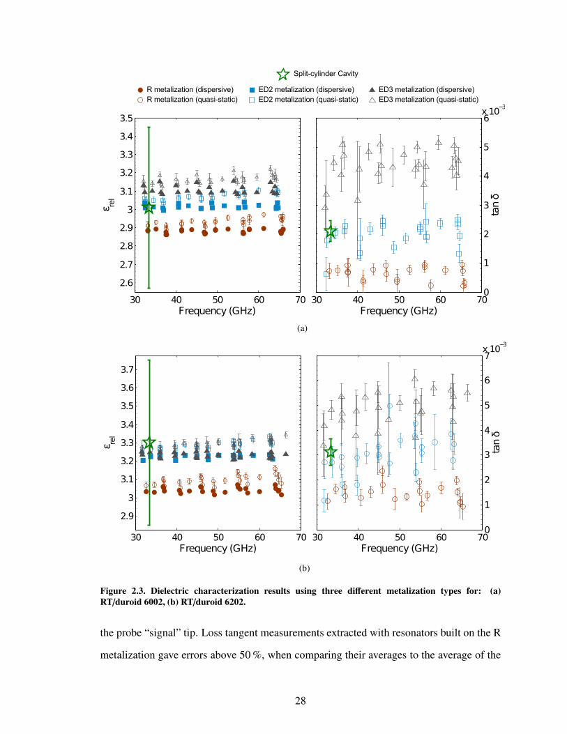
(a)
(b)
Figure 2.3. Dielectric characterization results using three di!erent metalization types for: (a)RT/duroid 6002, (b) RT/duroid 6202.
the probe “signal” tip. Loss tangent measurements extracted with resonators built on the R
metalization gave errors above 50 %, when comparing their averages to the average of the
28
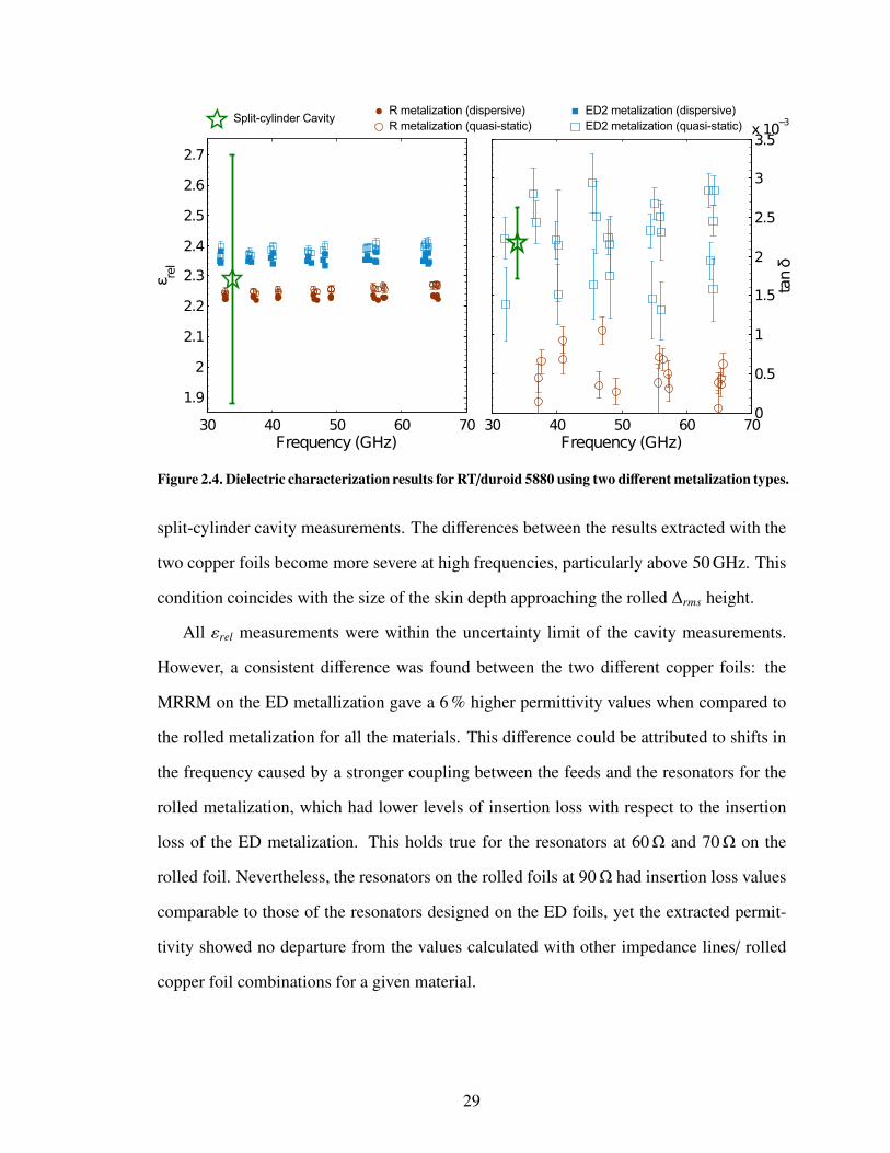
Figure 2.4. Dielectric characterization results for RT/duroid 5880 using two di!erent metalization types.
split-cylinder cavity measurements. The di!erences between the results extracted with the
two copper foils become more severe at high frequencies, particularly above 50 GHz. This
condition coincides with the size of the skin depth approaching the rolled $rms height.
All !rel measurements were within the uncertainty limit of the cavity measurements.
However, a consistent di!erence was found between the two di!erent copper foils: the
MRRM on the ED metallization gave a 6 % higher permittivity values when compared to
the rolled metalization for all the materials. This di!erence could be attributed to shifts in
the frequency caused by a stronger coupling between the feeds and the resonators for the
rolled metalization, which had lower levels of insertion loss with respect to the insertion
loss of the ED metalization. This holds true for the resonators at 60# and 70# on the
rolled foil. Nevertheless, the resonators on the rolled foils at 90# had insertion loss values
comparable to those of the resonators designed on the ED foils, yet the extracted permit-
tivity showed no departure from the values calculated with other impedance lines/ rolled
copper foil combinations for a given material.
29

CHAPTER 3
A LIGHTWEIGHT, ORGANIC PHASED ARRAY WITH
WIRE-BONDED ICS IN THE X BAND
A man grows with the magnitude of his task.
Man and his symbols, Dell, 1968
C. G. Jung
3.1 Introduction
Current and future trends in phased-array technologies for radar and communication ap-
plications have been broadly discussed in the available literature [73, 74] (among others).
Researchers agree that new developments in phased-array technology should be focused on
providing features such as light weight, active-circuit integration, reduced power consump-
tion, conformal mounting capability, scalability, and above all, low production cost. All
these features should be taken into account to achieve the best RF performance by maxi-
mizing the output power, the operation bandwidth and the antenna gain while minimizing
the noise figure (NF) of the system and optimizing the beam-steering range.
Besides simplifying interconnectivity through the integration of multiple active circuits
in a single chip at a reduced power consumption, SiGe BiCMOS IC solutions have shown
remarkable RF performance [24, 27] at a low production cost. These works demonstrate
that it is feasible to integrate phase shifters (PS) with low noise amplifiers (LNA) or with
power amplifiers (PA) in a single silicon die, thus, reducing the degradation of the RF
performance caused by numerous interconnections.
The aforementioned single-chip SiGe BiCMOS developments have allowed the recent
implementation of lightweight, receive-only phased arrays in the X and Ku frequency bands
[20, 25]. In these implementations, a PS and an LNA within a single SiGe IC are used to
drive individual [25] or several [20] radiating elements in the array. The true benefit of
30
these designs relies on the reduction of the NF of the system as it is significantly improved
by placing the active circuitry closer to the radiating elements.
Further weight and footprint size reduction has been achieved through vertical stacks of
organic substrates such as liquid crystal polymer (LCP) and duroid [20, 75]. Additionally,
vertical stack-ups of organic materials give physical flexibility which permits the conformal
mounting of the arrays without having to trade o! future scalability of the system to a higher
number of radiating elements. Moreover, vertical stack-ups also reduce the influence of the
beam-forming network over the radiation-pattern of the array given the ground plane that
separates them. The ground plane also allows flexibility of design as it is possible to use
di!erent substrate-thickness combinations for the beam-forming network and antennas. In
this manner, a thick, low-dielectric-constant substrate can be used for the radiating elements
to improve the antenna radiation e"ciency; and a thin, high-dielectric-constant substrate
can be used for the beam-forming network to reduce the width of the transmission lines,
the diameter of via-holes and the size of passive RF components.
The work presented in this chapter takes advantage of SiGe TRICs that incorporate an
LNA and a three-bit PS that can work in transmit (Tx) or receive (Rx) mode; and integrates
them with additional RF MEMS switches (henceforth, MEMS switches) and SiGe PAs to
create a full T/R array. A significant reduction in production costs is intended through the
use of high-performance low-cost components such as LCP substrates and silicon-based
ICs. To the best of the authors’ knowledge, this work demonstrated for the first time the
operation of a T/R 64-element phased array at 9.5 GHz using SiGe active circuitry and
MEMS switches in a lightweight LCP/ duroid stack-up. Design goals include a minimum
antenna operation bandwidth of 500 MHz and a minimum beam-steering range of ±25" in
the azimuthal direction.
31

3.2 System Overview
The simplified schematic diagram of the 64-element T/R phased array is shown in Figure
3.1. The beam-forming network of the array consists of 8 identical rows of active and
passive components, each driving a set of 8 microstrip patch antennas, therefore, forming
an 8x8 array configuration.
As illustrated in Figure 3.1, the Tx and Rx modes are determined in each row by the
state of the MEMS switch and of an integrated CMOS switch within the TRIC. In Tx mode
(shown), the internal CMOS switch routes the signal from the PS towards the PA, and the
MEMS switch, from the PA output towards the patch antennas. In Rx mode, the MEMS
switch routes the signal from the patch antennas towards the LNA, and the internal CMOS
switch, towards the PS. The TRIC PS is controlled by three “phase” bits that can establish
phase shifts of 45", 90" and 180", or any combination of them.
Figure 3.1. Simplified schematic of the T/R phased array with SiGe ICs indicated by dashed boxes.
The TRIC and PA were designed using a 130 nm SiGe BiCMOS process (IBM 8HP)
with ft of 200 GHz and fmax of 250 GHz. The TRIC design consisted of a single-stage, hy-
brid cascode topology with a (0.12 # 6 # 4) µm2 high-performance common emitter device
and a (0.12 # 18 # 8) µm2 common base high-breakdown device. This topology improves
output power and e"ciency due to the higher breakdown and better voltage knee. In addi-
tion, all input and output matching was performed on-chip. The PA on-chip bias circuitry
consists of a stable band-gap reference and switched current source that allows consistent
32
operation and quick power-cycle capacity.
Commercial single-pole, double-throw, RF MEMS switches (Radant RMSW220HPTM)
were used at the interface with the antenna-feed network. The switch provides an isolation
of 20 dB between the Tx output and the Rx input, and an insertion loss of less than 0.45 dB
at 10 GHz. It has a nominal power-handling capability at 10 GHz of 36 dBm in cold-
switching conditions.
Besides the integrated circuits, the beam-forming network includes two sets of multiple
3 dB splitters. The first set is used to distribute the RF signal to and from the 8 rows
containing the T/R circuitry, and the second set, to distribute the RF signal between 8 patch
antennas and a given T/R active module. The array elements were designed according to
the procedure presented in [20], to provide a constant gain across the broadside azimuthal
range between ±25".
3.2.1 Substrate Stack-up
The array was implemented in a vertical stack-up (shown in Figure 3.2) of the organic
substrates liquid crystal polymer (!rel = 2.95, tan " = 0.0025) and RT/duroid 5880 LZ
(!rel = 1.96, tan " = 0.002, henceforth duroid substrate). The metallization of all patterned
layers is done with copper (17µm). Transmission lines and ICs are respectively patterned
and mounted on an LCP stack-up that has a total thickness of 7 mil (177.8 µm). The LCP
stack is formed by a top LCP core with a thickness of 2 mil (LCP2 mil), and a bottom LCP
core of a thickness of 4 mil (LCP4 mil), laminated together through an intermediate LCP
bond-ply layer (1 mil). The RF feed network is patterned on the top side of LCP2 mil and
the antenna feed lines are patterned on the upper sides of LCP2 mil and LCP4 mil. The ground
plane of the transmission lines of the beam-forming network is at the bottom of LCP4 mil.
The LCP stack is separated from the duroid substrate through a copper ground plane
that has apertures to couple the patch antennas to the beam-forming network (Figure 3.2).
The duroid substrate is adhered to the ground plane with an LCP bond-ply layer (1 mil).
A novel feature of this design is the implementation of recessed cavities on LCP where
33

Figure 3.2. Cross section of the substrate stack-up showing only 2 patch antennas on the duroid sub-strate and the beam-forming network components in the LCP substrate.
the ICs of the system are mounted (shown in Fig.3.2). These cavities add robustness to
the design by protecting the ICs and by reducing the length of the bond wires that connect
the ICs to the RF transmission lines. Shorter bond wires consequently minimize undesired
insertion loss and parasitic e!ects.
3.2.2 Array Digital Control and Power Supply Module
An FPGA (field-programmable gate array) board digitally controls the states of the phase
bits along with the TRIC and MEMS switches. Arbitrary phase states and operation modes
can be set at any time through a customized computer interface. Three digital lines of 2.5 V
from the FPGA set the phase shift of single or multiple rows at a time, fully automating the
orientation of the main beam. An additional T/R digital line sets the state of the internal
switch of the TRIC for the Tx and Rx modes. Simultaneously, the T/R digital line also sets
the state of a custom-made driver card that toggles the MEMS switches between the Tx and
Rx modes.
In addition, a power-supply module was developed to apply feed voltages to the SiGe
active ICs on the antenna panel through custom-made cable assemblies. The power-supply
board generates 5 V and 3.5 V to respectively feed the common-collector and base bias
inputs of the eight PAs. The same 3.5 V output is used to feed the eight TRICs. The
5 V output feeds the MEMS driver card, which provides the switches with 85 V through
an external power supply. The total power consumed by all the active components of the
phased array is estimated at 601.3 mW.
34
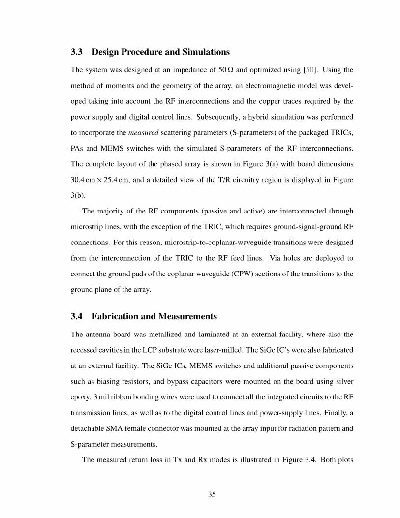
3.3 Design Procedure and Simulations
The system was designed at an impedance of 50# and optimized using [50]. Using the
method of moments and the geometry of the array, an electromagnetic model was devel-
oped taking into account the RF interconnections and the copper traces required by the
power supply and digital control lines. Subsequently, a hybrid simulation was performed
to incorporate the measured scattering parameters (S-parameters) of the packaged TRICs,
PAs and MEMS switches with the simulated S-parameters of the RF interconnections.
The complete layout of the phased array is shown in Figure 3(a) with board dimensions
30.4 cm # 25.4 cm, and a detailed view of the T/R circuitry region is displayed in Figure
3(b).
The majority of the RF components (passive and active) are interconnected through
microstrip lines, with the exception of the TRIC, which requires ground-signal-ground RF
connections. For this reason, microstrip-to-coplanar-waveguide transitions were designed
from the interconnection of the TRIC to the RF feed lines. Via holes are deployed to
connect the ground pads of the coplanar waveguide (CPW) sections of the transitions to the
ground plane of the array.
3.4 Fabrication and Measurements
The antenna board was metallized and laminated at an external facility, where also the
recessed cavities in the LCP substrate were laser-milled. The SiGe IC’s were also fabricated
at an external facility. The SiGe ICs, MEMS switches and additional passive components
such as biasing resistors, and bypass capacitors were mounted on the board using silver
epoxy. 3 mil ribbon bonding wires were used to connect all the integrated circuits to the RF
transmission lines, as well as to the digital control lines and power-supply lines. Finally, a
detachable SMA female connector was mounted at the array input for radiation pattern and
S-parameter measurements.
The measured return loss in Tx and Rx modes is illustrated in Figure 3.4. Both plots
35

(a)
(b)
Figure 3.3. Phased array layout: (a) Top view of metallization layers in the antenna board, and (b)close-up of T/R circuitry region.
demonstrate an antenna bandwidth below 10 dB across the 9.25 GHz-9.75 GHz band. In
fact, the total Tx bandwidth covers a band of about 2.675 GHz and the Rx bandwidth, of
2.43 GHz to give an average T/R operation bandwidth of 2.55 GHz, which exceeds the
design goal of 500 MHz.
The radiation pattern measurements were taken in a fully automated anechoic chamber
(Figure 3.5). The power supply/ digital control module was covered with RF absorbers to
36

Figure 3.4. Measured return loss of the phased array.
increase the accuracy of the measurements. A laptop computer was used to set the di!erent
phase states of the rows in the array. The results of the co-polarization measurements in
Rx mode with a maximum peak gain of 27.28 dB at boresight are depicted in Figure 6(a).
From the maximum gain lobe a broad-side, a 3 dB beam-width of approximately 10" is
observed. As expected, the peak gain decreases to 26.14 dB at an angle of 24", on the other
hand, the signal falls to 26.35 dB at $28", giving a receive beam-steering range of ±26".
Cross-polarization measurements were also performed and a maximum level 30 dB below
the maximum array gain was observed, indicating that the cross-polarization radiation is
negligible. In Tx mode, measurements showed (Figure 6(b)) a steering range of ±26.5" and
a peak gain of 18.57 dB at $11", followed by the slightly lower boresight gain (18.24 dB).
The 0.33 dB di!erence between these two peak gains is attributed to slightly dissimilar
operating points among the 8 PAs.
The EIRP can be calculated using the approach presented in [24]. However, this ap-
proach requires the knowledge of the gain of individual radiating elements in the array and
the losses of the network between the output of the PA and the antennas. Although the in-
dividual antenna gain and loss of the output network could be obtained through simulation,
an accurate calculation to estimate the EIRP is proposed here by referring the PA output
power at saturation to the RF feed of the phased array, and then applying the measured
transmit gain at boresight.
A hybrid simulation that took into account the simulated S-parameters of the input
37

Figure 3.5. Fabricated phased array and measurement setup.
network indicated that the insertion loss from the array feed to the output of one PA is
9.26 dB. Thus, added to the measured saturated power of the PA (13.5 dBm), the required
total input power becomes 22.76 dBm. This figure is then added to the maximum transmit
gain at boresight (18.57 dB) to obtain an estimated EIRP of 41.33 dBm.
38
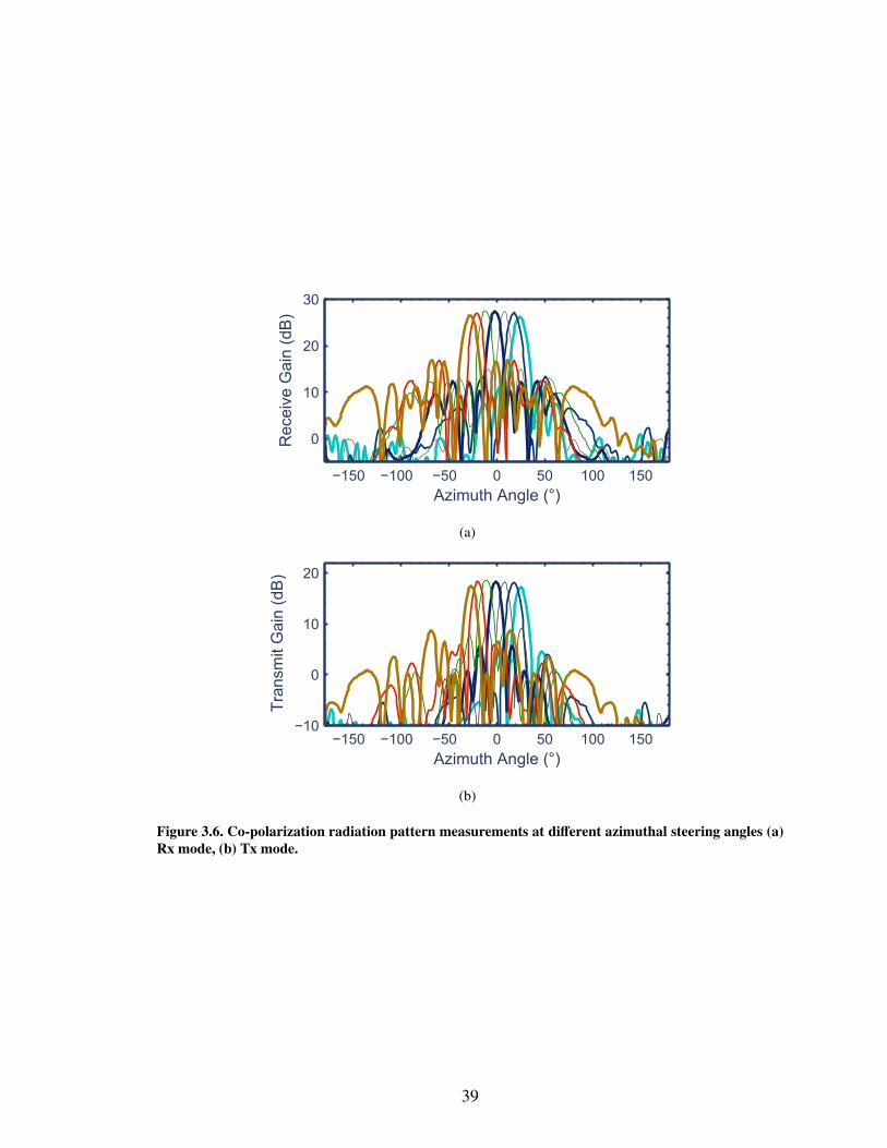
(a)
(b)
Figure 3.6. Co-polarization radiation pattern measurements at di!erent azimuthal steering angles (a)Rx mode, (b) Tx mode.
39
CHAPTER 4
DEVELOPMENT OF LOW-PROFILE INTERCONNECTS FOR
HIGHLY-INTEGRATED ORGANIC PHASED ARRAYS
4.1 Introduction
As it is desired in any antenna system, the distance between the radiating element and the
transmit receive circuitry must be minimized to decrease the noise figure in the receive side,
and to increase the e!ective isotropically irradiated power on the transmit side. Therefore,
the transmit-receive integrated circuit (TRIC) module must drive as few radiating elements
as possible to minimize further losses caused by the beam-former network (BFN) lines.
However, to maintain this short-distance condition in large arrays, the number of TRIC
modules must increase accordingly, which inevitably escalates the complexity of digital and
direct current (DC) interconnections necessary for the proper operation of these modules.
If improperly handled, cross-couplings between the radio frequency (RF) lines and the
DC/ digital lines can araise, a!ecting adversely the performance of densely-populated
antenna boards such as aperture-coupled phased arrays with integrated TRIC modules.
Hence, avoiding cross couplings is a major concern in low-profile antenna boards, where it
is preferable to have all the DC/ digital lines and the BFN in the same package as shown in
Figure 1.3.
In this chapter, the development of a stripline structure with via fences and of a Coplanar-
Waveguide-to-Stripline (CPW-SL) transition are introduced for SoP phased-array antenna
boards. The via fences minimize cross-couplings while suppressing undesired high-order
propagation modes. Stripline is defined in this work as a waveguide composed of “a center
strip located between two ground planes” [76]. The proposed BFN is implemented in the
organic material Rogers 3850 liquid crystal polymer (LCP) material with !rel = 2.95, and
tan " = 0.0025. LCP is well known for its lightweight, low-cost, flexibility, and excellent
broadband RF performance [20]. Its recent use in organic phased arrays [20, 75] motivates
40

the study of a stripline BFN for the development of low-cost, and lightweight SoP phased
arrays.
Two important contributions are made in this chapter. First, considering the concepts
introduced in [76, 77], and [78], Section 4.2.2 addresses the case for which the recom-
mended via spacing rule of [77] cannot be met because of manufacturing limitations. An
increased via spacing is desirable in multi-chip phased arrays to allow crossings of the DC/
digital lines over multiple areas of the BFN as shown in Figure 1.3.
The second contribution of this work is that it shows the fabrication feasibility of mul-
tilayer BFNs implemented in a lightweight, LCP-based organic package. Although several
misalignment issues have been published in multilayer LCP designs, the proposed BFN
transition shows promising immunity to interlayer misalignments below the Ku Band as it
will be seen in Section 4.2.3. The performance of the proposed stripline configuration and
of the CPW-SL transition is presented in Section 4.3 using various calibration schemes for
the measurements.
4.2 Design Procedure4.2.1 Stripline and Substrate Geometry
The chosen substrate stack for the proposed BFN is shown in Figure 4.1. The LCP stack
has two regions of interest: a Stripline Region, which is embedded in an LCP sub-stack
that has a total thickness of H = 8 mil (1 mil = 25.4 µm); and a DC/ digital Region, which
“caps” the stripline region and that would contain all the biasing and digital control lines
of the TRICs in the array.
The DC/ digital Region has an LCP core layer with a thickness of 1 mil, and it contains
the 1/2 oz copper layers M1 and “Top Ground Plane”. On the other hand, the Stripline
Region has an LCP core (with a thickness of h = 4 mil) that contains the 1/4 oz metal-
lization layers M2 and “Bottom Ground Plane”. The 1/2 oz metallization enhances current
handling capability of the bias traces in M1, while the 1/4 oz one allows the fabrication of
finer features in M2.
41
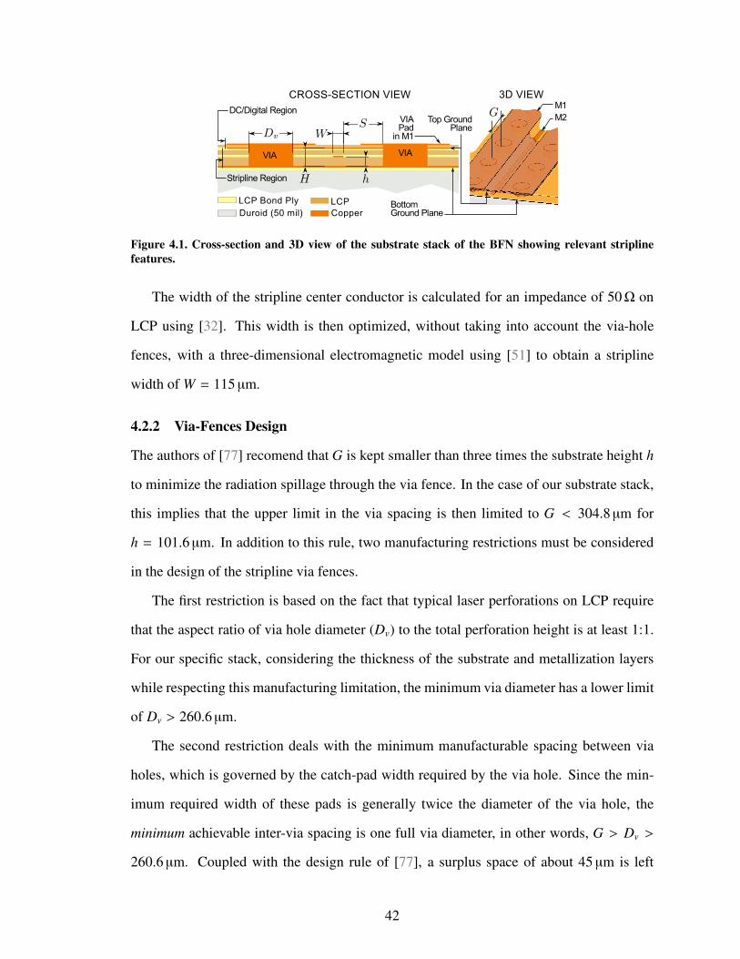
Figure 4.1. Cross-section and 3D view of the substrate stack of the BFN showing relevant striplinefeatures.
The width of the stripline center conductor is calculated for an impedance of 50# on
LCP using [32]. This width is then optimized, without taking into account the via-hole
fences, with a three-dimensional electromagnetic model using [51] to obtain a stripline
width of W = 115 µm.
4.2.2 Via-Fences Design
The authors of [77] recomend that G is kept smaller than three times the substrate height h
to minimize the radiation spillage through the via fence. In the case of our substrate stack,
this implies that the upper limit in the via spacing is then limited to G < 304.8µm for
h = 101.6 µm. In addition to this rule, two manufacturing restrictions must be considered
in the design of the stripline via fences.
The first restriction is based on the fact that typical laser perforations on LCP require
that the aspect ratio of via hole diameter (Dv) to the total perforation height is at least 1:1.
For our specific stack, considering the thickness of the substrate and metallization layers
while respecting this manufacturing limitation, the minimum via diameter has a lower limit
of Dv > 260.6µm.
The second restriction deals with the minimum manufacturable spacing between via
holes, which is governed by the catch-pad width required by the via hole. Since the min-
imum required width of these pads is generally twice the diameter of the via hole, the
minimum achievable inter-via spacing is one full via diameter, in other words, G > Dv >
260.6 µm. Coupled with the design rule of [77], a surplus space of about 45 µm is left
42

on M1 which, from a manufacturing perspective, is generally not su!cient to allocate the
necessary gaps and line widths in a 1/2 oz or in a 1/4 oz copper metallization.
Another approach that can be used to solve this problem is to look at it from a substrate
integrated waveguide (SIW) perspective [78]. Since the purpose of the via fence is to sup-
press the propagation of the parallel plate mode [76], with the addition of the via fences,
the problem turns into the design of a rectangular waveguide operating below the cut-o!
frequency of the T E10 mode ( fc,10). In other words, to prevent the propagation of rectangu-
lar waveguide modes, including the design rules given in [77]4.1, the distance a = 2S +W
must be chosen such that (correcting the relation introduced in [79]):
c0
2 · fc,10 ·(!rel
> a > 6H +W, (4.1)
where c0 is the speed of light in vacuum, and !rel, the relative permittivity of the stripline
substrate. For large antenna boards, minimizing the distance S is not of much concern and
thus, distances can be chosen arbitrarily within the range specified in (4.1) by fixing fc,10 to
a frequency that is well above the operation frequency range of the stripline.
Returning to the topic of interest of this discussion from an SIW perspective, [78] gives
an additional set of guidelines to select the diameter and pitch (defined as b = Dv + G) of
the via holes to minimize radiation spillage through the via posts inasmuch as undesired
coupling between adjacent lines. These conditions are:
Dv < $g/5, and b & 2Dv, (4.2)
where $g = c0/(!rel and f0 is the frequency of operation. Regardless of our choice of Dv,
(4.2) does not solve our problem either since using the maximum value recommended of b
sets G = Dv, which (as demonstrated) is not suitable for our manufacturing conditions.
In this work, the e!ect of increasing via size and via spacing with respect to all these
design guidelines is evaluated. Increased via size/ spacing has the added benefit of reducing
4.1In [77], the author suggests to place the via fences at a minimum distance of 3H from the signal stripedge
43
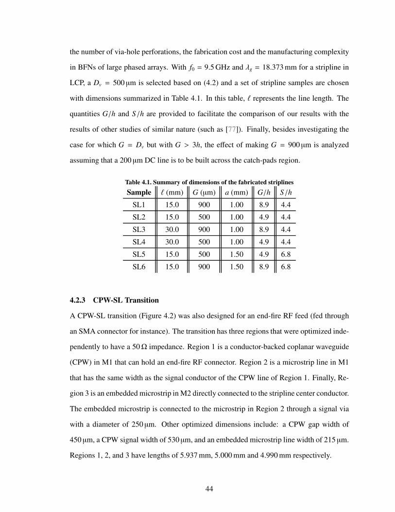
the number of via-hole perforations, the fabrication cost and the manufacturing complexity
in BFNs of large phased arrays. With f0 = 9.5 GHz and $g = 18.373 mm for a stripline in
LCP, a Dv = 500 µm is selected based on (4.2) and a set of stripline samples are chosen
with dimensions summarized in Table 4.1. In this table, + represents the line length. The
quantities G/h and S/h are provided to facilitate the comparison of our results with the
results of other studies of similar nature (such as [77]). Finally, besides investigating the
case for which G = Dv but with G > 3h, the e!ect of making G = 900 µm is analyzed
assuming that a 200 µm DC line is to be built across the catch-pads region.
Table 4.1. Summary of dimensions of the fabricated striplines
Sample + (mm) G (µm) a (mm) G/h S/h
SL1 15.0 900 1.00 8.9 4.4
SL2 15.0 500 1.00 4.9 4.4
SL3 30.0 900 1.00 8.9 4.4
SL4 30.0 500 1.00 4.9 4.4
SL5 15.0 500 1.50 4.9 6.8
SL6 15.0 900 1.50 8.9 6.8
4.2.3 CPW-SL Transition
A CPW-SL transition (Figure 4.2) was also designed for an end-fire RF feed (fed through
an SMA connector for instance). The transition has three regions that were optimized inde-
pendently to have a 50# impedance. Region 1 is a conductor-backed coplanar waveguide
(CPW) in M1 that can hold an end-fire RF connector. Region 2 is a microstrip line in M1
that has the same width as the signal conductor of the CPW line of Region 1. Finally, Re-
gion 3 is an embedded microstrip in M2 directly connected to the stripline center conductor.
The embedded microstrip is connected to the microstrip in Region 2 through a signal via
with a diameter of 250 µm. Other optimized dimensions include: a CPW gap width of
450 µm, a CPW signal width of 530 µm, and an embedded microstrip line width of 215 µm.
Regions 1, 2, and 3 have lengths of 5.937 mm, 5.000 mm and 4.990 mm respectively.
44
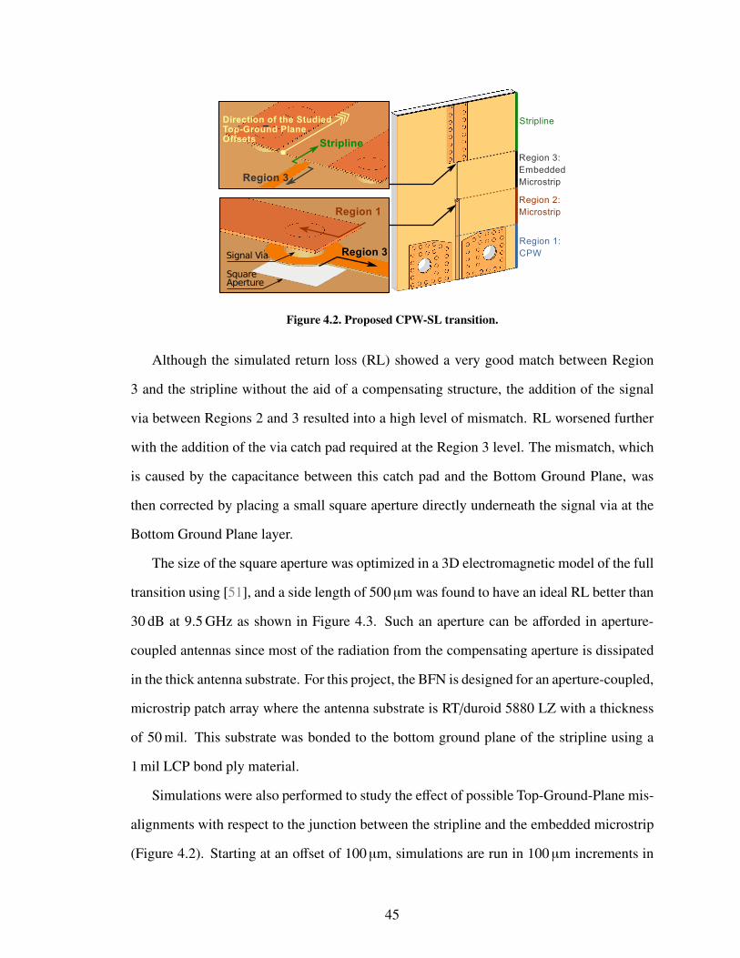
Figure 4.2. Proposed CPW-SL transition.
Although the simulated return loss (RL) showed a very good match between Region
3 and the stripline without the aid of a compensating structure, the addition of the signal
via between Regions 2 and 3 resulted into a high level of mismatch. RL worsened further
with the addition of the via catch pad required at the Region 3 level. The mismatch, which
is caused by the capacitance between this catch pad and the Bottom Ground Plane, was
then corrected by placing a small square aperture directly underneath the signal via at the
Bottom Ground Plane layer.
The size of the square aperture was optimized in a 3D electromagnetic model of the full
transition using [51], and a side length of 500 µm was found to have an ideal RL better than
30 dB at 9.5 GHz as shown in Figure 4.3. Such an aperture can be a!orded in aperture-
coupled antennas since most of the radiation from the compensating aperture is dissipated
in the thick antenna substrate. For this project, the BFN is designed for an aperture-coupled,
microstrip patch array where the antenna substrate is RT/duroid 5880 LZ with a thickness
of 50 mil. This substrate was bonded to the bottom ground plane of the stripline using a
1 mil LCP bond ply material.
Simulations were also performed to study the e!ect of possible Top-Ground-Plane mis-
alignments with respect to the junction between the stripline and the embedded microstrip
(Figure 4.2). Starting at an o!set of 100 µm, simulations are run in 100 µm increments in
45

Figure 4.3. Simulated response of the CPW-SL transition.
the direction shown in Figure 4.2 until an o!set of 500 µm is reached. Although RL de-
graded proportionally to the amount of o!set introduced, simulations showed (Figure 4.3)
that even for an o!set of 500 µm, the RL is still below 20 dB at 9.5 GHz, predicting a
promising post-fabrication performance.
4.3 Measurements
The fabricated samples SL4 and SL6 are presented in Figure 4.4. For these samples, Re-
gion 1 of Figure 4.2 is replaced by a smaller CPW probing pad that has the same CPW
dimensions described above. To better understand the performance of the stripline, two
thru-reflect-line (TRL) calibration sets were designed: TRL1, which de-embeds the total-
ity of the transition; and TRL2, which de-embeds Regions 1 and 2 setting the reference
plane right before the signal via that connects the microstrip to the embedded microstrip.
TRL1 stripline measurements are shown in Figure 4.5. As the TRL1 calibration sets the
reference impedance to that of the embedded microstrip, a match with an RL better than
20 dB is demonstrated between the stripline and the embedded microstrip. As expected, the
longest lines SL3 and SL4 have the highest insertion loss (IL), which is 0.80 dB at 9.5 GHz.
Moreover, the loss of all the lines is estimated at 0.26 dB/cm. TRL2 measurements gave
similar results, showing that internal matching of the system is excellent from the stripline
up to the microstrip (including the signal via interconnection).
A quick inspection of Figure 4.5 hints that the choice of G/h and S/h has little e!ect on
46
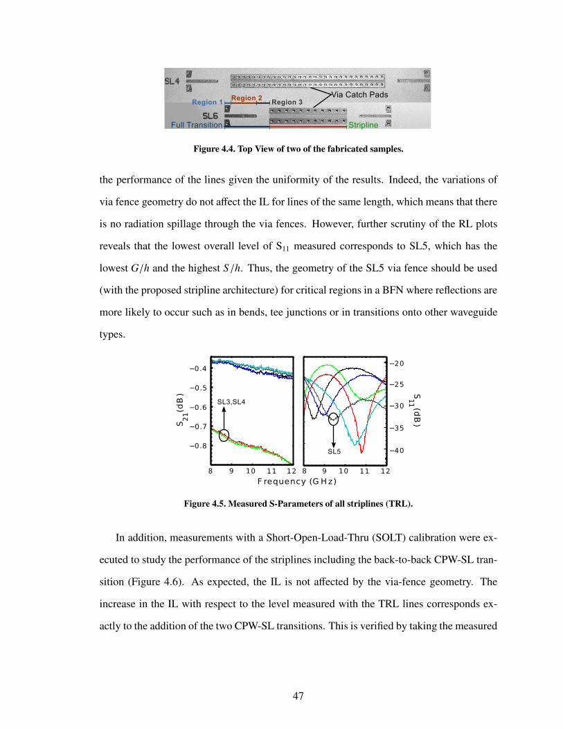
Figure 4.4. Top View of two of the fabricated samples.
the performance of the lines given the uniformity of the results. Indeed, the variations of
via fence geometry do not a!ect the IL for lines of the same length, which means that there
is no radiation spillage through the via fences. However, further scrutiny of the RL plots
reveals that the lowest overall level of S11 measured corresponds to SL5, which has the
lowest G/h and the highest S/h. Thus, the geometry of the SL5 via fence should be used
(with the proposed stripline architecture) for critical regions in a BFN where reflections are
more likely to occur such as in bends, tee junctions or in transitions onto other waveguide
types.
Figure 4.5. Measured S-Parameters of all striplines (TRL).
In addition, measurements with a Short-Open-Load-Thru (SOLT) calibration were ex-
ecuted to study the performance of the striplines including the back-to-back CPW-SL tran-
sition (Figure 4.6). As expected, the IL is not a!ected by the via-fence geometry. The
increase in the IL with respect to the level measured with the TRL lines corresponds ex-
actly to the addition of the two CPW-SL transitions. This is verified by taking the measured
47
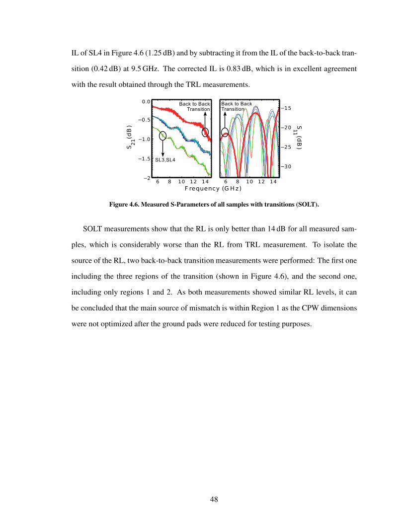
IL of SL4 in Figure 4.6 (1.25 dB) and by subtracting it from the IL of the back-to-back tran-
sition (0.42 dB) at 9.5 GHz. The corrected IL is 0.83 dB, which is in excellent agreement
with the result obtained through the TRL measurements.
Figure 4.6. Measured S-Parameters of all samples with transitions (SOLT).
SOLT measurements show that the RL is only better than 14 dB for all measured sam-
ples, which is considerably worse than the RL from TRL measurement. To isolate the
source of the RL, two back-to-back transition measurements were performed: The first one
including the three regions of the transition (shown in Figure 4.6), and the second one,
including only regions 1 and 2. As both measurements showed similar RL levels, it can
be concluded that the main source of mismatch is within Region 1 as the CPW dimensions
were not optimized after the ground pads were reduced for testing purposes.
48
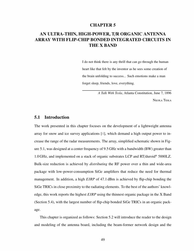
CHAPTER 5
AN ULTRA-THIN, HIGH-POWER, T/R ORGANIC ANTENNA
ARRAY WITH FLIP-CHIP BONDED INTEGRATED CIRCUITS IN
THE X BAND
I do not think there is any thrill that can go through the human
heart like that felt by the inventor as he sees some creation of
the brain unfolding to success... Such emotions make a man
forget sleep, friends, love, everything.
A Talk With Tesla, Atlanta Constitution, June 7, 1896
Nicola Tesla
5.1 Introduction
The work presented in this chapter focuses on the development of a lightweight antenna
array for snow and ice survey applications [4], which demand a high output power to in-
crease the range of the radar measurements. The array, simplified schematic shown in Fig-
ure 5.1, was designed at a center frequency of 9.5 GHz with a bandwidth (BW) greater than
1.0 GHz, and implemented on a stack of organic substrates LCP and RT/duroidR! 5880LZ.
Bulk-size reduction is achieved by distributing the RF power over a thin and wide-area
package with low-power-consumption SiGe amplifiers that reduce the need for thermal
management. In addition, a high EIRP of 47.1 dBm is achieved by flip-chip bonding the
SiGe TRICs in close proximity to the radiating elements. To the best of the authors’ knowl-
edge, this work reports the highest EIRP using the thinnest organic package in the X Band
(Section 5.4), with the largest number of flip-chip bonded SiGe TRICs in an organic pack-
age.
This chapter is organized as follows: Section 5.2 will introduce the reader to the design
and modeling of the antenna board, including the beam-former network design and the
49
Figure 5.1. Simplified schematic diagram of the proposed antenna array.
SiGe TRIC technology; in Section 5.3, the organic antenna board fabrication along with
the flip-chip bonding process of the SiGe TRICs are reported; and, in Section 5.4, the small-
and large-signal characterization of the active antenna board are reported, concluding with
a benchmark comparison to similar active arrays.
5.2 Array Design
In contrast to previous generations of this array technology [16, 20, 21, 80], significant
packaging innovations on the BFN side have allowed a higher level of integration and an
ultra low-profile in the proposed array. In this regard, one key achievement has been the
successful deployment of a multilayer, stripline BFN over a large antenna panel, following
the lamination scheme introduced in small scale in Chapter 4. Because a degradation in
the inter-layer alignment accuracy is expected for larger panel sizes (especially for organic
substrates such as LCP), the design of a BFN scheme with a performance that is immune
to fabrication misalignments is crucial to the operation of the array.
A multilayer fabrication was necessary in this work because the RF signal needed to be
confined into the substrate stack so that the performance of the system would not be a!ected
at crossing points with the Digital/ DC lines, which run mostly across the top metallization
50

layer of this stack. By allowing the multilayer overlap of RF and Digital/DC signals on the
same package, the total number of external connectors in this board is reduced to only two:
one SMA connector for the RF feed and one Digital/ DC 9-pin connector, which contains
all the necessary lines to operate the 32 SiGe TRICs.
The general operation of the array can be summarized by following the schematic in
Figure 5.1. The RF feed section of the array includes an end-fire SMA connector that is
directly connected to a multilayer CPW-to-stripline transition, which feeds the stripline
section of the BFN. The design and characterization of this multilayer CPW-to-stripline
transition have been thoroughly discussed in [79]. The stripline section then branches out
to 32 paths distributing the RF signal to each SiGe TRIC, which allow the toggled trans-
mit (Tx) and receive (Rx) operation. The interconnection to the SiGe TRICs is achieved
through single-layer stripline-to-CPW transitions. Finally, each SiGe TRIC is in turn cou-
pled to a pair of microstrip patch antennas via embedded microstrip lines and slot apertures
in the ground plane (Figure 5.2).
Figure 5.2. Cross-section view of the array substrate stack showing the conceptual distribution of com-ponents (the thickness of the metallization and substrate layers are shown in parentheses).
5.2.1 Substrate Stack Details
The detailed anatomy of the substrate stack and the conceptual distribution of the RF com-
ponents for one of the 32 active RF paths in the array is shown in the cross-section diagram
of Figure 5.2. This substrate stack architecture was briefly introduced in Chapter 4, and
is described in detail below within the context of this application. Following Figure 5.2,
51

the stack has a total thickness of 1.80 mm (including the height of the SiGe TRICs) and
contains three major regions:
• The Digital/ DC Region, which is implemented on a LCP core laminate (LCP Core
1) with top (M1) and bottom (M2) copper metallization. M1 contains the TRICs’
Digital/ DC lines, and the section of the RF feed that connects the BFN to the input
SMA connector. M2 contains the top ground plane pattern of the stripline BFN.
• The BFN Region, which is implemented using two LCP core laminates (LCP Core
2 and LCP Core 3), bonded altogether and to the Digital/ DC Region through LCP
bond-ply laminates. The LCP Core 3 has a copper metallization on its top (M3) and
bottom (M4) faces. M3 contains all the stripline and embedded microstrip compo-
nents of the BFN, along with the pads on which the SiGe TRICs are mounted. M4 is
the bottom ground plane of the RF lines of the array BFN, and has the slot apertures
that couple the embedded microstrip lines to the microstrip patch antennas. M4 is
also the ground plane of the microstrip patch antennas on the duroid substrate.
• Finally, the Antenna Region, which is implemented on an RT/duroidR! 5880LZ core
laminate that is bonded to the bottom ground plane of the BFN Region with a Taconic
fastRiseTM27 prepreg laminate (!rel = 2.75, and tan " = 0.0014) [81]. The 64 mi-
crostrip patch antennas are patterned on the copper metallization layer M5, which is
at the bottom face of the duroid substrate.
5.2.2 Stripline BFN
As shown in Figure 5.1, the majority of the BFN components of the proposed array are
implemented using stripline transmission lines. Via fences are deployed along the stripline
network to prevent the excitation of higher order modes and the coupling of electromagnetic
radiation onto Digital/ DC lines. The via fences were designed according to the geometries
introduced by the authors in [79], which follow the guidelines presented in [77] and [78].
Extending the results from [79], the design and simulated performance are introduced here
52

for key elements in the BFN, namely, the 3 dB power splitter, the eight-way power splitter,
and the single-layer stripline-to-CPW transitions for TRIC interconnection.
The basic building block of the corporate BFN is the stripline 3 dB splitter (Figure 5.3),
which provides an impedance match to 50# looking into the BFN. Quarter-wavelength
transformers were used at the junction to present two parallel 100# impedances from Ports
2 and 3, which reduce to a 50# load at Port 1. The length and width of the adapters are
obtained initially with [32] and then optimized with [51].
Figure 5.3. Multilayer top view of the stripline 3 dB splitter.
The ability of the via fences to provide the proper confinement of the RF signal in
the BFN was also investigated. For this purpose, an eight-way splitter (Figure 5.4) was
developed using [82], based on the 3 dB splitter geometry proposed above. The results
of a quick time-domain simulation confirm that proper RF-signal confinement is attained
by showing that the squared magnitude of the intensity of the electric field (|E|2, plotted
in Figure 5.4) reaches a level of $90 dB at the fence edges with respect to the maximum
|E|2, which occurs along the stripline signal conductor as expected. An S 11 match lower
than $20 dB is achieved across the band of interest (Figure 5.5). Including conductor and
dielectric losses, the total insertion loss of a single branch is found from simulation at
4.52 dB, which along with the 9.03 dB from the power splits add up to the simulated value
of S X1 = $13.6 dB (with X = {2, 3...9}).
Finally, to provide interconnectivity to the SiGe TRICs, a stripline-to-CPW transition
was developed. The proposed multilayer packaging scheme requires that each SiGe TRIC
is housed in a recessed cavity that goes through LCP Core 1 and LCP Core 2, to access the
53

Figure 5.4. Electromagnetic model of the stripline eight-way splitter and distribution of |E|2.
Figure 5.5. Simulated S parameters of the stripline eight-way splitter.
RF signal conductor in M3. Hence, a 3D electromagnetic model was developed in [51] and
is shown in Figure 5.6. The only criteria in the design of this final transition was to provide
a CPW section that is compatible with the pitch of the pins of the SiGe TRIC (250 µm)
and that can provide ground interconnectivity for the TRIC. The designed 50# CPW line
has a signal width of 210 µm and a gap width of 217 µm. Additionally, a short taper with
a length of 100 µm is provided to compensate for the width change in the signal conductor
at the interconnection with the stripline. The simulated S-parameter response is shown in
Figure 5.7.
5.2.3 SiGe TRIC Technology and Packaged Performance
In comparison to the case presented by the authors in [21] where the T/R module consisted
of three separate chips (plus required DC lumped-element components), the present work
introduces a single-chip, custom-made T/R module to meet the array real-estate require-
ments. The chip includes a three-bit phase shifter (PS), a low-noise amplifier (LNA), a
54

Figure 5.6. Electromagnetic model of the stripline-to-CPW transition (duroid substrate not shown).
Figure 5.7. Simulated S-parameters of the stripline-to-CPW transition.
power amplifier (PA), and two complementary metal oxide (CMOS) switches for full T/R
operation (Figure 8(a) and Figure 8(b)). Input and output matching is also performed on
die.
(a) (b)
Figure 5.8. T/R integrated circuit (TRIC): (a) block diagram and (b) circuit-layout photograph.
With a compact T/R module, the distance between the radiating elements and the TRIC
can be minimized and the EIRP, maximized. Although devices such as microelectrome-
chanical system (MEMS) switches or RF circulators would reduce the loss between the
55
radiating elements and the TRIC, the space and interconnection requirements would trans-
late into an impractical assembly process in the proposed scheme.
The TRICs were fabricated at an external facility using the same SiGe technology
as in [21]. Since the TRICs were designed to be flip-chip bonded to the antenna board,
controlled-collapse chip connection solder bumps (C4 bumps) [83] were placed on all in-
put/ output pads during fabrication. The chip occupies a space of 2.13 mm # 3.70 mm # 0.25 mm
, and the spherical C4 bumps have an approximated diameter of 100 µm. The LNA, digi-
tal control and PS sections require a bias voltage of 3.5 V and the PA section, 5.0 V. The
maximum DC power consumption of the TRIC is 400 mW in Tx mode.
As on-die testing of the SiGe TRICs was not possible because of the C4 bumps, a num-
ber of chips were mounted on individual packages that resembled packaging conditions of
the antenna. A comparison between the measured S parameters of a single flip-chip bonded
TRIC and the measured S parameters from four flip-chip bonded TRICs with epoxy under-
fill is presented in Figure 5.9. In these plots, the measurements with epoxy underfill mate-
rial are represented by the average S parameters from the four chips, calculated according
to [84].
The measurements included a thru-reflect-line calibration [52] to de-embed the measurement-
fixture transitions and lines up to the plane of the C4 bumps. From the S-parameter mea-
surements of the epoxy-under-filled samples at 9.5 GHz, in Rx mode an average S 21 of
6.56 dB was observed with a chip-to-chip variation from 6.41 dB to 6.73 dB, and in Tx
mode, an average S 21 of 1.01 dB with a variation from 1.36 dB to 0.50 dB. The e!ect of
the epoxy underfill on the return loss of the TRICs can also be noted in Figure 5.9. The
presence of the epoxy underfill slightly improves the return loss on the RF-feed side, and
degrades it on the radiating-elements side. More importantly, it can be observed that there
is an increase in insertion loss of about 0.5 dB in Rx mode and 1.1 dB in Tx mode with
respect to measurements of the TRIC without epoxy underfill. This is due to the interaction
of the epoxy underfill with the on-die circuit of the TRIC.
56

Figure 5.9. Measured S-parameters of singly-packaged TRICs in Tx and Rx mode, with and withoutepoxy underfill.
Noise figure (NF), TRIC output power (Pout) and gain compression measurements were
also performed on five singly-packaged TRICs with epoxy underfill. The average Rx-mode
noise figure is shown in Figure 5.10 over frequency. In Tx mode, gain compression and
TRIC Pout measurements are shown in Figure 5.11 per input-power level. In Rx mode, an
average NF * 5.4 dB is measured from 9.0 GHz to 10.0 GHz, with a chip-to-chip variation
from 4.97 dB to 5.87 dB. Finally, the Tx mode measurement at 9.5 GHz showed that the
average TRIC Psat * 11 dBm, with a variation from 9.67 dBm to 11.5 dBm.
5.2.4 Microstrip Patch Antennas
Since the proposed active array has a large and intricate design, the total BFN simulation
has been broken into individual components up to this point, ensuring that the 50# match
57
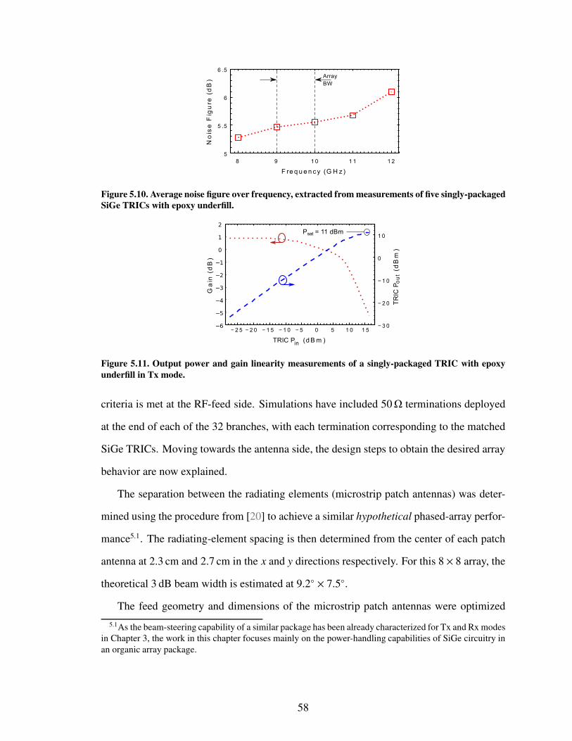
Figure 5.10. Average noise figure over frequency, extracted from measurements of five singly-packagedSiGe TRICs with epoxy underfill.
Figure 5.11. Output power and gain linearity measurements of a singly-packaged TRIC with epoxyunderfill in Tx mode.
criteria is met at the RF-feed side. Simulations have included 50# terminations deployed
at the end of each of the 32 branches, with each termination corresponding to the matched
SiGe TRICs. Moving towards the antenna side, the design steps to obtain the desired array
behavior are now explained.
The separation between the radiating elements (microstrip patch antennas) was deter-
mined using the procedure from [20] to achieve a similar hypothetical phased-array perfor-
mance5.1. The radiating-element spacing is then determined from the center of each patch
antenna at 2.3 cm and 2.7 cm in the x and y directions respectively. For this 8 # 8 array, the
theoretical 3 dB beam width is estimated at 9.2" # 7.5".
The feed geometry and dimensions of the microstrip patch antennas were optimized
5.1As the beam-steering capability of a similar package has been already characterized for Tx and Rx modesin Chapter 3, the work in this chapter focuses mainly on the power-handling capabilities of SiGe circuitry inan organic array package.
58

using [50], with the target of minimizing the S 11 at the RF feed plane across the desired
bandwidth. As done in [20], a baseline simulation was performed by replacing the TRICs
with 50# thru lines until an acceptable S 11 was obtained. Optimized dimensions are shown
in Figure 5.12.
Figure 5.12. Multilayer top view of the feed layout for a pair of patch-antennas.
5.3 Array Fabrication Process
Vertically-integrated antenna arrays, in particular arrays of slot-coupled, microstrip-patch
antennas, are versatile structures in the sense that distinct substrates can be used for the
radiating elements and for the BFN, which allows the optimization of the antenna re-
sponse while reducing the size of BFN components. As introduced in [85] and success-
fully demonstrated in [16,21,80], the higher dielectric constant and thin lamination of LCP
allows the reduction of the size of RF transmission lines and transitions on the BFN side,
while the lower dielectric constant and thick-lamination capacity of the duroid substrate
permit to attain a higher antenna bandwidth and a better radiation e"ciency [85].
Although in theory the two-substrate approach for vertically-integrated antennas may
seem like an optimal solution, major drawbacks were found during the practical implemen-
tation of this concept using distinct organic substrates. With di!erent dielectric constants,
the thermal-expansion coe"cient mismatch between the substrates will cause an undesired
tangential stress during heating and cooling cycles in post-lamination processing, which re-
sults in severe board warping of thin substrate stacks. The stress may weaken solder joints
in flip-chip bonded components if proper preemptive measures are not implemented.
59

Besides thermal issues during fabrication, the substrate stack must provide enough me-
chanical robustness to support the flip-chip bonded components. In this context, flip-chip
bonded approaches such as the one proposed in [17] did not prove suitable for our applica-
tion, as the thin dielectric and the silver epoxy solder joints would not keep the ICs securely
bonded to the larger package. Therefore, the key manufacturing and assembly steps that
allowed the implementation of the proposed array are introduced below.
5.3.1 Antenna Board Lamination
The antenna board lamination process started by etching the metallization patterns on the
LCP Cores (Figure 5.2). Prior to lamination, a thin electroless nickel immersion gold
(ENIG) coating was applied to M3 and to M5 to prevent oxidation on the metal layers
exposed to the environment, and to improve the reliability of the solder joints of the SiGe
TRICs. After the LCP Cores were patterned, these were pressed together at 285 "C using
the two LCP bond-ply laminates forming altogether the BFN and Digital/ DC Regions
shown in Figure 5.2.
Subsequently, the bonded LCP regions were pressed together with the duroid substrate
using the fastRiseTM27 prepreg laminate. A LCP bond ply is not used in this step be-
cause it would require a 285 "C process that would cause the bond ply laminates used in
the BFN region to melt again and hence, deteriorate the alignment of the LCP Cores. The
fastRiseTM27 prepreg laminate has a lower melting temperature and, being considerably
thinner (50 µm) than the duroid substrate (1.27 mm), has little e!ect on the antenna per-
formance. After board lamination, laser via-hole perforations were done in the LCP layers
and then copper plated to provide the necessary BFN Region interconnections. Finally, an
ENIG finish was applied to the M1 metallization.
The TRIC recessed cavities were then laser milled onto the BFN Region. As conven-
tional laser perforations in organic substrates are either hollow through cuts or are cuts
terminated in a solid metal sheet, terminating a recessed cavity in a metallization pattern
60
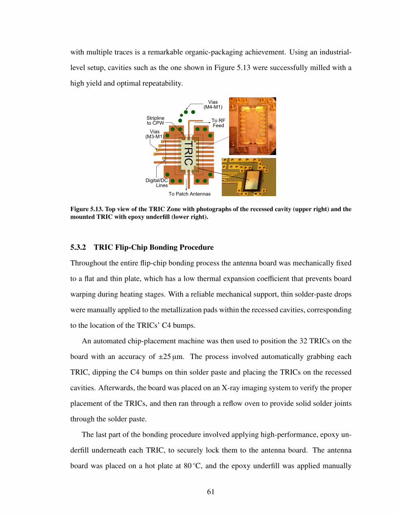
with multiple traces is a remarkable organic-packaging achievement. Using an industrial-
level setup, cavities such as the one shown in Figure 5.13 were successfully milled with a
high yield and optimal repeatability.
Figure 5.13. Top view of the TRIC Zone with photographs of the recessed cavity (upper right) and themounted TRIC with epoxy underfill (lower right).
5.3.2 TRIC Flip-Chip Bonding Procedure
Throughout the entire flip-chip bonding process the antenna board was mechanically fixed
to a flat and thin plate, which has a low thermal expansion coe"cient that prevents board
warping during heating stages. With a reliable mechanical support, thin solder-paste drops
were manually applied to the metallization pads within the recessed cavities, corresponding
to the location of the TRICs’ C4 bumps.
An automated chip-placement machine was then used to position the 32 TRICs on the
board with an accuracy of ±25 µm. The process involved automatically grabbing each
TRIC, dipping the C4 bumps on thin solder paste and placing the TRICs on the recessed
cavities. Afterwards, the board was placed on an X-ray imaging system to verify the proper
placement of the TRICs, and then ran through a reflow oven to provide solid solder joints
through the solder paste.
The last part of the bonding procedure involved applying high-performance, epoxy un-
derfill underneath each TRIC, to securely lock them to the antenna board. The antenna
board was placed on a hot plate at 80 "C, and the epoxy underfill was applied manually
61
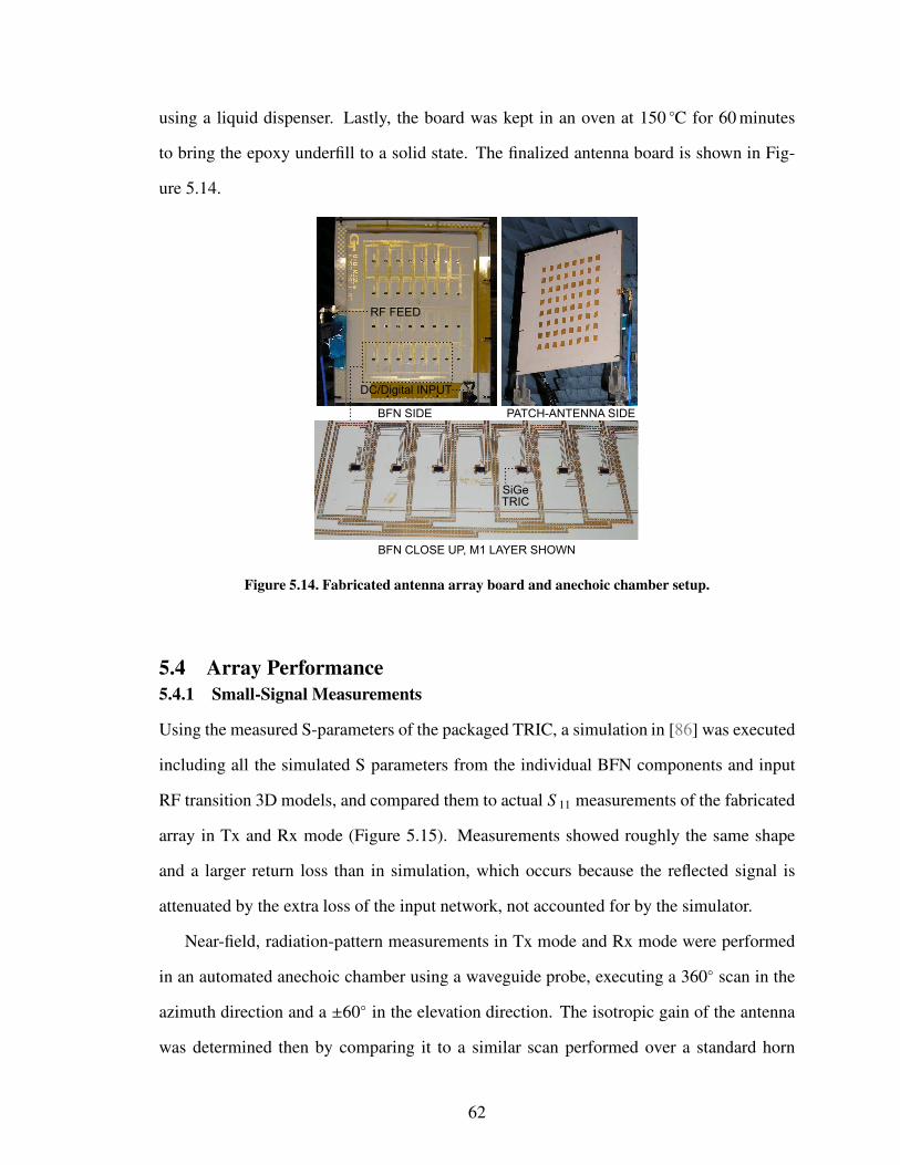
using a liquid dispenser. Lastly, the board was kept in an oven at 150 "C for 60 minutes
to bring the epoxy underfill to a solid state. The finalized antenna board is shown in Fig-
ure 5.14.
Figure 5.14. Fabricated antenna array board and anechoic chamber setup.
5.4 Array Performance5.4.1 Small-Signal Measurements
Using the measured S-parameters of the packaged TRIC, a simulation in [86] was executed
including all the simulated S parameters from the individual BFN components and input
RF transition 3D models, and compared them to actual S 11 measurements of the fabricated
array in Tx and Rx mode (Figure 5.15). Measurements showed roughly the same shape
and a larger return loss than in simulation, which occurs because the reflected signal is
attenuated by the extra loss of the input network, not accounted for by the simulator.
Near-field, radiation-pattern measurements in Tx mode and Rx mode were performed
in an automated anechoic chamber using a waveguide probe, executing a 360" scan in the
azimuth direction and a ±60" in the elevation direction. The isotropic gain of the antenna
was determined then by comparing it to a similar scan performed over a standard horn
62

Figure 5.15. Measured and simulated S 11 of the proposed antenna array in Tx and Rx modes.
antenna. The near-field measurements were post-processed using [87], and considering
the e"ciency of the BFN, the far-field gain radiation patterns were obtained in Tx and Rx
modes (Figure 5.16). The measured broadside Rx gain is 20.1 dBi, and Tx gain, 14.6 dBi
at 9.5 GHz.
Figure 5.16. Estimated far-field radiation pattern based on near-field measurements in the azimuthaldirection.
Given that a large number of on-board DC and RF interconnects motivated the usage of
63
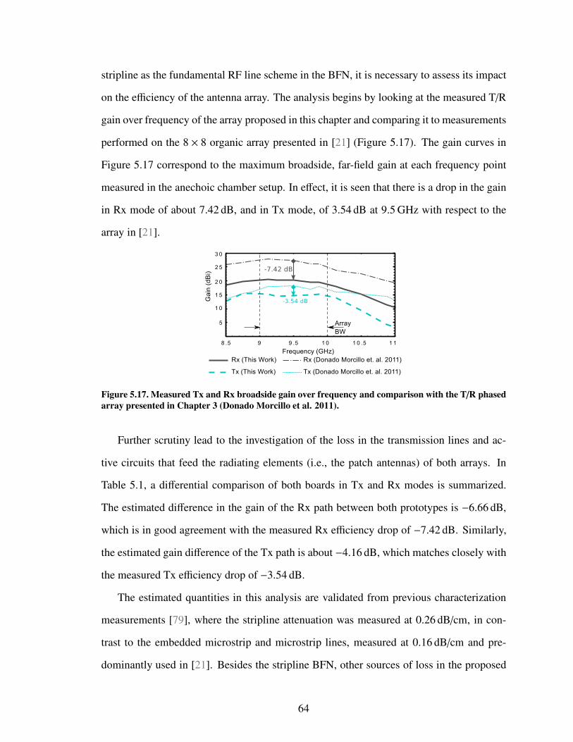
stripline as the fundamental RF line scheme in the BFN, it is necessary to assess its impact
on the e"ciency of the antenna array. The analysis begins by looking at the measured T/R
gain over frequency of the array proposed in this chapter and comparing it to measurements
performed on the 8 # 8 organic array presented in [21] (Figure 5.17). The gain curves in
Figure 5.17 correspond to the maximum broadside, far-field gain at each frequency point
measured in the anechoic chamber setup. In e!ect, it is seen that there is a drop in the gain
in Rx mode of about 7.42 dB, and in Tx mode, of 3.54 dB at 9.5 GHz with respect to the
array in [21].
Figure 5.17. Measured Tx and Rx broadside gain over frequency and comparison with the T/R phasedarray presented in Chapter 3 (Donado Morcillo et al. 2011).
Further scrutiny lead to the investigation of the loss in the transmission lines and ac-
tive circuits that feed the radiating elements (i.e., the patch antennas) of both arrays. In
Table 5.1, a di!erential comparison of both boards in Tx and Rx modes is summarized.
The estimated di!erence in the gain of the Rx path between both prototypes is $6.66 dB,
which is in good agreement with the measured Rx e"ciency drop of $7.42 dB. Similarly,
the estimated gain di!erence of the Tx path is about $4.16 dB, which matches closely with
the measured Tx e"ciency drop of $3.54 dB.
The estimated quantities in this analysis are validated from previous characterization
measurements [79], where the stripline attenuation was measured at 0.26 dB/cm, in con-
trast to the embedded microstrip and microstrip lines, measured at 0.16 dB/cm and pre-
dominantly used in [21]. Besides the stripline BFN, other sources of loss in the proposed
64
Table 5.1. Comparison of the e"ciency drop between the proposed array and the T/R array presentedin Chapter 3
Parameter at 9.5 GHz [21] This work Di!erence
BFN Single-Path
Passive S 21 (dB)-5.27 -10.94 -5.66
LNA + PS S 21 (dB) 7.5 6.5 -1.00
Calculated Rx PathS 21 (dB)
-15.77 -22.44 -6.66
Measured Rx
E"ciency (dB)1.57 -5.85 -7.42
PA + PS S 21 (dB) 0.0 1.5 +1.5
Calculated Tx PathS 21 (dB)
-23.27 -27.44 -4.16
Measured TxE"ciency (dB)
-7.74 -11.28 -3.54
array include a longer feed network, a larger number of transitions, deployment of epoxy
underfill, and the integration of a CMOS switch in the radiating-element side of the TRIC.
It is important to observe that, despite the drop in small-signal gain, the high level
of integration of the TRICs and the stripline BFN did allow the incorporation of a large
number of TRICs on the antenna board only a few cm away from the radiating elements.
This strategic technology change caused a significant improvement in the EIRP, as will be
seen next.
5.4.2 Large-Signal Measurements
To verify the large-signal performance of the proposed array (henceforth the antenna under
test or AUT, with Tx gain GAUT ) and to measure its EIRP, three point-to-point links were
set up using two additional reference antennas as follows:
• Configuration A: Reference horn antenna 1 (RHA1, with gain GRHA1) in the Rx end
and AUT in the Tx end.
• Configuration B: Reference horn antenna 2 (RHA2, with gain GRHA2) in the Rx end
65
and AUT in the Tx end.
• Configuration C: RHA2 in the Rx end and RHA1 in the Tx end.
The purpose of this experiment, illustrated in Figure 5.18, is to build a system of three
link-budget equations with the gains of each antenna as the unknowns:
GAUT +GRHA1 = CA [dB] (5.1)
GAUT +GRHA2 = CB [dB] (5.2)
GRHA1 +GRHA2 = CC [dB], (5.3)
where Cn = PRx+LRx+FS L$Pin (with n = {A, B,C}) for each measurement configuration.
Here, PRx is the Rx power measured by the spectrum analyzer; LRx, the Rx cable loss; and
FS L, the free space loss of the point-to-point link. The system is then solved at di!erent
frequency points and levels of input power on the Tx end.
The measurements were performed outdoors, and RF absorbers were deployed in strate-
gic positions to minimize reflections that could introduce systematic errors to the measure-
ments. A distance of 7.95 m was left between the Tx and Rx antennas, which is well above
the far field distance of the AUT5.2. In addition, the phase center of all the antennas was
kept within a height of 1.5 m from the floor level. Environmental conditions were also
monitored on the Tx side vicinity with temperatures ranging between 13 "C and 16 "C and
relative humidity, between 49 % and 55 %.
On the Tx side, a signal generator was used with a high-power amplifier (HPA) to
provide the necessary Pin at di!erent frequencies. Considering the BFN loss and the power
splits, a theoretical Pin = 35.1 dBm is necessary at the RF-feed plane to drive all TRIC PAs
into compression in Tx mode. On the Rx side, the reference horn antennas were connected
to an Agilent PXA spectrum analyzer through a coaxial cable (Rx cable).
5.2With an AUT maximum dimension of D = 30.5 cm at $ = c/9.5 GHz, where c is the speed of light invacuum, the estimated far-field distance 2D2/$ = 5.89 m.
66

Figure 5.18. Schematic diagram of EIRP measurement Configuration A and Configuration B.
Prior to the outdoor tests, laboratory measurements were carried out to characterize
each component of the Tx and Rx back-ends. The output power of the Tx back end (signal
generator+HPA+RF cables) was characterized by connecting it directly to the spectrum
analyzer, and measuring all Pin levels for the test frequencies and signal generator output-
power levels. Likewise, the Rx cable was characterized through S-parameter measurements
with a network analyzer.
A Pin sweep was performed from 0.0 dBm to 37.3 dBm at 9.5 GHz, over 15 measure-
ment points. Solutions to the link-budget system of equations showed an average RHA1
gain of 16.57 dBi with a standard deviation of 0.08 dBi —nominal gain declared by the
manufacturer of (16.50 ± 0.75) dBi; and an average RHA2 gain of 12.91 dBi with a stan-
dard deviation of 0.14 dBi —nominal gain declared by the manufacturer between 13.0 dBi
and 13.5 dBi from 9.0 GHz to 10.0 GHz. The AUT Tx gain was found at 14.45 dBi (com-
pared to the anechoic chamber measurements at 14.6 dBi) for low levels of Pin, compressing
all the way to 9.7 dBi for a Pin = 37.3 dBm.
Having found the gains of each antenna for each power level, the maximum EIRP
emitted by the proposed array can be determined from (5.1) and (5.2) as follows:
EIRP = PRx + LRx $GRHA + FS L, (5.4)
where GRHA is the gain of the reference horn antenna for a given configuration. Calcu-
lations show that EIRP saturates at maximum values of 46.9 dBm and 47.1 dBm, using
67

Configuration A and Configuration B respectively. Figure 5.19 summarizes the EIRP mea-
surements from Configuration A and Configuration B at 9.5 GHz, compared with the ideal
EIRP curve that assumes an AUT small-signal gain of 14.45 dBi for all Pin levels.
Figure 5.19. Measured EIRP with Configuration A and Configuration B for various values of Pin.
Figure 5.20. Measured EIRP over frequency using Configuration A for Pin = 36.2 dBm.
A similar treatment was applied to measurements carried out over frequency to find out
the EIRP at each frequency point (Figure 5.20). To investigate the behavior of the array
in high-Tx power over frequency, a measurement scan was carried out with Configuration
A over 10 measurement points from 9 GHz to 10 GHz, with Pin = 36.2 dBm. The results
of this test are presented in Figure 5.20, where an average EIRP of 46.7 dBm is observed
with a standard deviation of 0.8 dB over this frequency band.
5.4.3 Estimation of G/T
The noise figure (NF) of the array in Rx mode is calculated through the following equation
from [88]:
NF = Lf F $ Lf /g + Lf Lc/g, (5.5)
68
where Lf represents the loss of the transmission line between the radiating elements and
the SiGe TRIC (i.e., the loss of the embedded microstrip line); F and g, the noise figure
and gain of the TRIC in receive mode respectively; and Lc, the loss between the RF feed
and the TRIC (stripline BFN and CPW-to-stripline transition). All quantities are positive
real scalars greater than one (no dB quantities must be used).
The G/T antenna figure of merit is then calculated using the following expression, also
from [88]:
G/T =DA
Ti + T0(NF $ 1), (5.6)
where T0 (the system temperature) is assumed to be equal to Ti (the temperature at which
the antenna is pointed at) and equal to the room temperature of 290 K.
With Lf = 0.36 dB, g = 6.50 dB, F = 5.4 dB and Lc = 10.58 dB, the noise figure of
the array in Rx mode is estimated at 7.99 dB. Hence, with a measured array directivity of
25.98 dB, a figure of merit G/T = $6.64 dB is obtained.
5.4.4 Comparison With Other Works
Including the proposed array, various state-of-the-art antenna arrays implemented in or-
ganic packages are presented in Table 5.2, where several performance parameters are com-
pared. Some of the key parameters to notice are the Rx gain, the maximum EIRP attained,
the DC power consumption and the total package thickness. In this last parameter, the
antenna-board thickness considers only the height of the package including the compo-
nents in the T/R module, but excluding antenna-board input/output connectors.
Some of the quantities in Table 5.2 are estimated based on the observation of the pho-
tographs of the devices presented in the references, as the authors did not give enough
information to fill in the table. Since the fabrication of active Tx antenna arrays using or-
ganic substrates is a relatively new topic and as most of the literature available covers Tx
only or Rx only arrays, it was challenging to choose meaningful benchmark parameters to
compare di!erent devices.
69

Table 5.2. State-of-the-art organic antenna arrays
Reference This WorkArray in
Chapter 3[22] [23] [24]
No. of RadiatingElements
64 64 8 16 16
No. of Tx or T/RModules
32 8 8 8 16
No. ofComponents per
Tx or T/R module1 chip
3 chips +lumped
elements
5 chips +lumped
elements
+12 chips +lumped
elements1 chip
Design Frequency(GHz)
9.5 9.5 1.26 3.3 51.0 to 65.0
DeclaredBandwidth (GHz)
> 1.0 > 1.0 0.08 0.40 -
RF Functionality T/RT/R Phased
ArrayT/R Phased
ArrayTx only
Tx PhasedArray
Max. DC PowerConsumption in Tx
Mode (W)12.8 0.60 -
47.6 (per T/Rmodule)
6.4
Max. EIRP atDesign Frequency
(dBm)47.1 42.5 - 44.0 40.0
EIRP Assessment Measurement Calculation -Measurement
(per arraycell)
Measurement
Rx Broadside Gainat Design
Frequency (dBi)14.6 18.6 - - -
Rx NF at DesignFrequency (dB)
7.99 7.20 - - -
G/T (dB) $6.64 $6.09 - - -
Total Package Area(cm2)
30.5 # 25.4 30.4 # 25.4 112 # + 60 18.29 # 18.29 2.8 # 2.8
ApproximateThickness (mm)
1.8 + 1.82 + 0.1 , 5.0 + 0.2
Packaging SchemeSoP,
LCP+duroidSoP,
LCP+duroidSoP,
Pyralux R! APTMSoP, Rogers
4350BTM SoC, BGA
Active CircuitTechnology
SiGeSiGe +MEMS
GaAs GaN SiGe
On the Tx side, the proposed array exhibits the thinnest package and achieves the high-
est EIRP in the X-band. On the Rx side, although the estimated G/T of this work is com-
petitive in comparison to other works, better performance in Rx mode could be attained
70

by reducing the loss of the BFN. Calculations show that by replacing 10 cm of stripline by
embedded microstrip, the insertion loss of the BFN can be decreased by 3 dB, which would
in turn result in a 1.1 dB increase in G/T .
71

CHAPTER 6
THERMAL ASPECTS IN THE DESIGN OF LIGHTWEIGHT
RADAR FRONT-ENDS
I mean that you always know what results will come from one
or another of your actions; but in a strange way you want to do
one thing and get the result that could only come from another
Strange Life of Ivan Osokin, 1947
P.D. Ouspensky
6.1 Introduction
The increase of EIRP in the active arrays of Chapter 3 and in Chapter 5 revealed the need to
explore the performance of lightweight and low cost organic substrates under high-power
conditions. This investigation is motivated by several factors, but mainly by the fact that
little work has been performed in modeling the thermal behavior of organic substrates in
the microwave domain.
Just as it is the case of low-frequency electronics, RF circuits will generally under-
perform at high temperatures because of the reduction of the electrical conductivity of
the metal, the increase in tan ", the changes in the !rel, and finally, the variations in the
circuitry geometry caused by thermal expansion. In this context, proper thermal modeling
at high frequencies should consider schemes where the high temperature in the environment
a!ects the RF device, where high RF power drives causes self-heating e!ects, or where
the temperature raise is caused by the heat dissipated by active devices integrated in the
package (such as in the instance of PAs with low operating e"ciency).
A good example of the last case, is illustrated by anecdotal experience in the imple-
mentation of the Tx functionality in the array of Chapter 3. Prior to the successful SiGe
PA deployment, the original intent was to package gallium arsenide (GaAs) PAs using the
72

wire-bonded approach shown in Figure 1.4, with the substrate stack up of Figure 3.2. How-
ever, the low e"ciency of the GaAs PA in conjunction with the low thermal conductivity
of the duroid (Kduroid = 0.33 Wm$1"C$1) and LCP (KLCP = 0.2 Wm$1"C$1) [8] substrates,
and the thin copper metalization lead in multiple occasions to the thermal breakdown of
the device.
Besides understanding the heat-sinking capacity of these organic substrates, it is also
important to understand how the dielectric properties change over temperature to accu-
rately predict performance degradation in extreme environments. Changes in the !rel and
tan ", caused by either self-heating or heating from the environment, can result in undesired
frequency shifts or unacceptable levels of insertion loss, which may render microwave com-
ponents useless under high temperature.
Insights on the design of microstrip circuits considering their thermal performance are
presented in this chapter. A thermal assessment of microstrip structures on a number of
thin films of interest is presented in Section 6.2, and, the thermal properties of the organic
thin film RT/duroid 6002 from 30 GHz to 70 GHz are reported in Section 6.3.
6.2 Analytical Assessment of the Power-Handling Capacity of Thin-
Film Substrates6.2.1 Thermal Analysis Formulation
A conventional approach for analyzing the thermal behavior of microstrip circuits under
high RF power was developed by Bahl and Gupta in 1979 [89,90]. In this formulation, the
authors drew thermal analogies to microstrip closed-form models to analytically predict
the temperature rise of the circuits and their average power handling capacity (APHC) of
microstrip lines.
The methodology developed in [89] yielded to the thermal assessment of microstrip
lines on polymide and other thin-film substrates [91,92], and of substrate-integrated waveg-
uide (SIW) structures on duroid and Polystyrene [93], with a similar approach used in
the assessment of a circular dielectric waveguide on PTFE [94]. In all these works, the
73
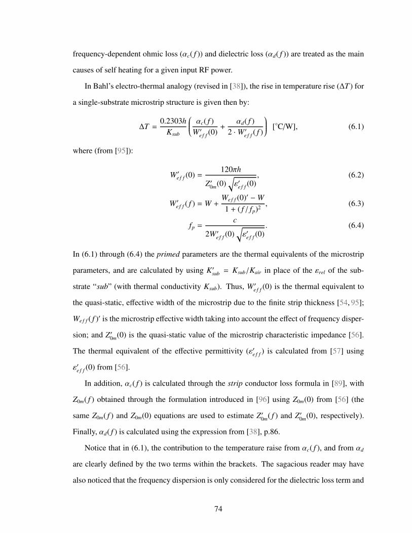
frequency-dependent ohmic loss ((c( f )) and dielectric loss ((d( f )) are treated as the main
causes of self heating for a given input RF power.
In Bahl’s electro-thermal analogy (revised in [38]), the rise in temperature rise ($T ) for
a single-substrate microstrip structure is given then by:
$T =0.2303h
Ksub
ABBBBC(c( f )
W )e f f
(0)+
(d( f )
2 ·W )e f f
( f )
DEEEEF ["C/W], (6.1)
where (from [95]):
W )e f f (0) =
120%h
Z)0m(0)
#!)
e f f(0), (6.2)
W )e f f ( f ) = W +
We f f (0)) $W
1 + ( f / fp)2, (6.3)
fp =c
2W )e f f
(0)#!)
e f f(0). (6.4)
In (6.1) through (6.4) the primed parameters are the thermal equivalents of the microstrip
parameters, and are calculated by using K)sub = Ksub/Kair in place of the !rel of the sub-
strate “sub” (with thermal conductivity Ksub). Thus, W )e f f (0) is the thermal equivalent to
the quasi-static, e!ective width of the microstrip due to the finite strip thickness [54, 95];
We f f ( f )) is the microstrip e!ective width taking into account the e!ect of frequency disper-
sion; and Z)0m(0) is the quasi-static value of the microstrip characteristic impedance [56].
The thermal equivalent of the e!ective permittivity (!)e f f ) is calculated from [57] using
!)e f f (0) from [56].
In addition, (c( f ) is calculated through the strip conductor loss formula in [89], with
Z0m( f ) obtained through the formulation introduced in [96] using Z0m(0) from [56] (the
same Z0m( f ) and Z0m(0) equations are used to estimate Z)0m( f ) and Z)0m(0), respectively).
Finally, (d( f ) is calculated using the expression from [38], p.86.
Notice that in (6.1), the contribution to the temperature raise from (c( f ), and from (d
are clearly defined by the two terms within the brackets. The sagacious reader may have
also noticed that the frequency dispersion is only considered for the dielectric loss term and
74

not for the ohmic loss. This assumption is valid according to [89] because the spread of the
electric field lines within the dielectric (and thus, for the heat flow in the dielectric) are a
function of frequency, which is not the case for the ohmic loss that is confined to the signal
strip itself.
With the calculated $T , the APHC (Pav) required to trigger a temperature change from
Tamb (ambient temperature) to Tmax (maximum temperature of operation of a given sub-
strate) is given by:
Pav =Tmax $ Tamb
$T[W]. (6.5)
6.2.2 Thermal Assessment Results
The main purpose of this assessment is to use the formulation of Section 6.2 to investigate
the thermal behavior of some of the thin films of interest, and to determine a proper scheme
to increase the output power of the RF front ends while maintaining a lightweight and a low
profile. The APHC is shown in Figure 1(a) for 50# lines implemented on LCP with com-
mercial vaues of metallization thickness and substrate height for a maximum temperature
raise of 225 "C (the LCP-bond-ply melting temperature) and 275 "C (the melting tempera-
ture of the LCP core laminate). The power required to drive the LCP into a temperature of
100 "C for the same geometries is illustrated in Figure 1(b).
Suppose that the high-power active array from Chapter 5 is to be integrated with other
three similar arrays to increase directivity and output power from 50 W to 200 W. To
implement such a system some form of power distribution system, such as an n-way
Wilkinson power divider (WPD), would be required to distribute the RF energy. From Fig-
ure 6.2.2 it becomes clear that a 200 W is beyond the capacity of 50# lines implemented
on commercially-available LCP thin films.
Even though LCP is a low-loss substrate it has a limited power-handling capability
that is predominantly driven by its low thermal conductivity. To overcome this thermal
limitation and to take advantage of its low cost and lightweight, two paths can be taken.
75

(a) (b)
Figure 6.1. APHC for various geometries of 50# lines on LCP laminates with a thickness (t) of 2 mil,4 mil and 8 mil: (a) APHC for LCP’s temperature limits, and (b) APHC for a Tmax = 100 "C.
The first path involves the design of hybrid solutions using components that are capable
of handling high power while maintaining a lightweight and low profile in crucial parts of
the system. These components may be implemented in higher cost, rigid substrates such as
ceramics, since their larger relative permittivity will allow higher levels of integration than
with their organic counterparts. The second path involves developing innovative thermal
management solutions that can be implemented in a low-profile architecture such as liquid
cooling using micro channels [97–100].
Comparing LCP’s thermal performance with the performance of other substrates such
as aluminum nitride (AlN) or alumina (Al2O3), the APHC trends for temperature raise of
100 "C of 50# lines implemented on substrates with commercially-available geometries
are illustrated in Figure 6.2. A metal thickness of 4.5 µm has been assumed for all cases,
using copper as the LCP metallization, and gold for alumina and AlN.
AlN was investigated because of its high thermal conductivity6.1, which coupled to its
low loss yields to a high APHC. The use of this substrate was proposed by Eyring in 1991
6.1In this assessment, two commercially-available thermal conductivities for AlN were investigated:KAlN = 80 Wm$1"C$1 and KAlN = 230 Wm$1"C$1
76

Figure 6.2. APHC (Tamb = 25 "C, f = 10 GHz) comparison of 50# transmission lines between commer-cially-available geometries of di!erent dielectric substrates.
[101] for Wilkinson power dividers utilizing tantalum nitride (TaN) thin-film resistors. It
can be observed in Figure 6.2 that the APHC of AlN outperforms that of alumina, even for
AlN’s lowest commercially-available thermal conductivity. Considering the high APHC of
AlN, the design of n-way Wilkinson power dividers is presented in Appendix A.
It is also interesting to note that for a 25 mil substrate thickness, the AlN material with
KAlN = 80 Wm$1"C$1 has a similar APHC as the alumina substrate, even though alumina
has a lower thermal conductivity. This is due to the fact that AlN is a lossier material than
alumina at 10 GHz, and at this thickness, the dielectric losses tend to dominate over the
thermal conductivity. Table 6.1 summarizes the RF and thermal properties of the substrates
studied, and Table 6.2 summarizes the parameters calculated with the models in Section 6.2.
77
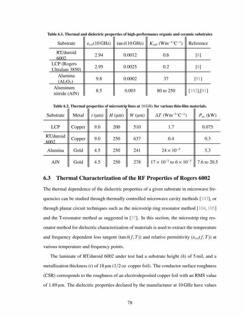
Table 6.1. Thermal and dielectric properties of high-performance organic and ceramic substrates
Substrate !rel(10 GHz) tan "(10 GHz) Ksub (Wm$1"C$1) Reference
RT/duroid6002
2.94 0.0012 0.6 [8]
LCP (RogersUltralam 3850)
2.95 0.0025 0.2 [8]
Alumina(Al2O3)
9.8 0.0002 37 [91]
Aluminum
nitride (AlN)8.5 0.003 80 to 250 [102],[91]
Table 6.2. Thermal properties of microstrip lines at 10 GHz for various thin-film materials.
Substrate Metal t (µm) H (µm) W (µm) $T (Wm$1"C$1) Pav (kW)
LCP Copper 9.0 200 510 1.7 0.075
RT/duroid6002
Copper 9.0 250 637 0.4 0.3
Alumina Gold 4.5 250 241 24 # 10$3 5.3
AlN Gold 4.5 250 278 17 # 10$3 to 6 # 10$3 7.6 to 20.5
6.3 Thermal Characterization of the RF Properties of Rogers 6002
The thermal dependence of the dielectric properties of a given substrate in microwave fre-
quencies can be studied through thermally controlled microwave cavity methods [103], or
through planar circuit techniques such as the microstrip ring resonator method [104, 105]
and the T-resonator method as suggested in [37]. In this section, the microstrip ring res-
onator method for dielectric characterization of materials is used to extract the temperature
and frequency dependent loss tangent (tan "( f , T )) and relative permittivity (!rel( f , T )) at
various temperature and frequency points.
The laminate of RT/duroid 6002 under test had a substrate height (h) of 5 mil, and a
metallization thickness (t) of 18 µm (1/2 oz copper foil). The conductor surface roughness
(CSR) corresponds to the roughness of an electrodeposited copper foil with an RMS value
of 1.89 µm. The dielectric properties declared by the manufacturer at 10 GHz have values
78
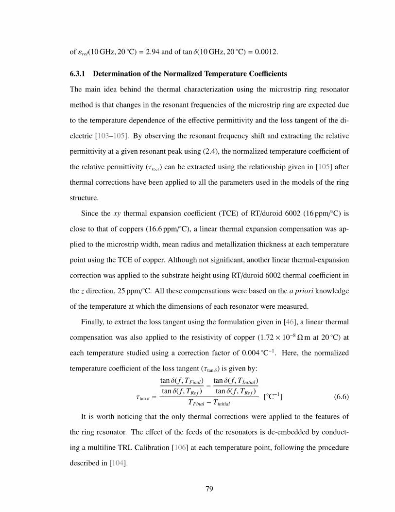
of !rel(10 GHz, 20 "C) = 2.94 and of tan "(10 GHz, 20 "C) = 0.0012.
6.3.1 Determination of the Normalized Temperature Coe"cients
The main idea behind the thermal characterization using the microstrip ring resonator
method is that changes in the resonant frequencies of the microstrip ring are expected due
to the temperature dependence of the e!ective permittivity and the loss tangent of the di-
electric [103–105]. By observing the resonant frequency shift and extracting the relative
permittivity at a given resonant peak using (2.4), the normalized temperature coe"cient of
the relative permittivity (#!rel) can be extracted using the relationship given in [105] after
thermal corrections have been applied to all the parameters used in the models of the ring
structure.
Since the xy thermal expansion coe"cient (TCE) of RT/duroid 6002 (16 ppm/"C) is
close to that of coppers (16.6 ppm/"C), a linear thermal expansion compensation was ap-
plied to the microstrip width, mean radius and metallization thickness at each temperature
point using the TCE of copper. Although not significant, another linear thermal-expansion
correction was applied to the substrate height using RT/duroid 6002 thermal coe"cient in
the z direction, 25 ppm/"C. All these compensations were based on the a priori knowledge
of the temperature at which the dimensions of each resonator were measured.
Finally, to extract the loss tangent using the formulation given in [46], a linear thermal
compensation was also applied to the resistivity of copper (1.72 # 10$8#m at 20 "C) at
each temperature studied using a correction factor of 0.004 "C$1. Here, the normalized
temperature coe"cient of the loss tangent (#tan ") is given by:
#tan " =
tan "( f , TFinal)
tan "( f , TRe f )$
tan "( f , TInitial)
tan "( f , TRe f )
TFinal $ Tinitial
["C$1] (6.6)
It is worth noticing that the only thermal corrections were applied to the features of
the ring resonator. The e!ect of the feeds of the resonators is de-embedded by conduct-
ing a multiline TRL Calibration [106] at each temperature point, following the procedure
described in [104].
79

If a TRL calibration was not performed at each temperature point, a di"cult analytical
de-embedding procedure would have to be applied to eliminate the e!ect of the feeds.
Such a de-embedding procedure would have to take into account geometrical deformations
of the feeds, changes in the e!ective permittivity of the transmission lines and changes in
conductivity of the metallization due to the heating of the sample.
6.3.2 Design and Fabrication of the Test Circuits
The design and fabrication of the test circuits was performed according to the guidelines
given in [46] and [106]. Two microstrip ring resonators were fabricated at line impedances
of 60# and at 70#, with fundamental resonances of 8.55 GHz and of 8.08 GHz respec-
tively. Both structures were fabricated on di!erent wafers of the same laminate of RT/duroid
6002.
To achieve a frequency resolution that would allow the observation of the resonant
frequency shifts due to the heating of the material, the measurement bandwidth was split
in two portions: from 30 GHz to 48.5 GHz and from 48.5 GHz to 67 GHz. Two calibration
lines were designed to have an e!ective electrical length of 90" at two frequencies in each
of the two portions of the total measurement bandwidth.
6.3.3 Measurement Procedure
Measurements were conducted with an Agilent Performance Network Analyzer (PNA)
model E8361C, and the samples were measured on a Karl Suss PM5 Thermal Chuck prob-
ing station. The temperature control was provided by a Temptronic Corporation TPO315A-
TS-1 temperature controller.
Four temperature points were tested with each sample. S-Parameter measurements
were taken with the 60# sample at 20 "C, 80 "C, 140 "C and 200 "C, and with the 70#
sample at 20 "C, 80 "C, 140 "C and 175 "C. Two TRL calibrations were performed at each
temperature point: one for each frequency bandwidth portion described above. The PNA
was set to a sweep time of 5 s, an IF bandwidth of 300 Hz and a number of 1601 points.
80

The circuits were probed using ground-signal-ground (GSG) probes of 250 µm pitch and
the software package MulticalTM from the National Institute of Standards and Technology
was used to process the calibration and to de-embed the feeds of the resonators.
During the 60# resonator measurements the thermal chuck was kept at a distance of
about 3 cm below the probes to avoid heating the probes for a long period of time and
to avoid their damage. However, this created undesired S-Parameter responses at 200 "C
where the circuit only gave reasonable results at the end of the bandwidth, i.e., after being
connected to the circuit for a few seconds. Thus, only the measurements of the resonance
at about 60.05 GHz were kept at this temperature.
After observing undesired calibration results using the 60#methodology at the highest
temperature point, during the 70# resonator measurements, the probes were kept a few
millimeters over the thermal chuck to minimize the e!ect of the heating in the measure-
ment of the calibration standards and the resonator. The temperature range was reduced by
replacing the last point at 200 "C, measuring at 175 "C instead. The change in methodology
gave better calibration results at all temperature points tested.
The measurements were made at least 20 min after fixing the temperature at each mea-
surement temperature point. The temperature changes on the substrate were measured
using a thermocouple at the ground plane (bottom) and another at the circuit metallization
(top) to guarantee that the substrate had a uniform temperature (see Figure 6.3.3). During
measurements, and as noted in [103], the small gaps between the sensors and the surface
to be measured create large temperature di!erentials and erroneous temperature measure-
ments. To avoid temperature measurement errors, further adherence between the sample
and the chuck was provided with thermal tape (in addition to the chuck vacuum), and
high-temperature, thermal conducting paste was deployed to stick the thermocouples to the
wafer metallization.
In addition to the thermocouples, a thermo-hygrometer was placed in the environment
surrounding the sample to measure the changes in humidity (Figure 6.3.3). The relative
81

(a)
(b) (c)
Figure 6.3. (a) Measurement-setup cross section (b) probing and performance network analyzer, and(c) detail of the area surrounding the sample.
humidity in the vicinity of the chuck changed from 20 % at room temperature to 5 % at
the last temperature point of each sample measurement. Although it was documented, the
e!ect of humidity was not accounted for in the calculations.
6.3.4 Measurement Results
The results extracted from the measurements, visualized in in Figure 6.4 and Figure 6.5, are
summarized in Table 6.3. The normalization of the temperature coe"cients of the relative
permittivity and loss tangent on Table 1 was performed by dividing the slope of the linear
fit of each of the frequency data sets in Figure 6.4 and Figure 6.5, by the values of the
82

Table 6.3. Extracted normalized temperature coe"cients for !rel( f ) and tan "( f ) for RT/duroid 6002 forTre f = 20 "C from 30 GHz to 70 GHz
Frequency (GHz) #!rel(ppm/"C) #tan " ("C$1)
32.61 -19.9 0.0081
40.69 -29.2 0.0133
48.81 -16.0 0.0179
56.84 -16.0 0.0073
64.84 -18.6 0.0106
e!ective permittivity and relative permittivity at Tre f = 20 "C, respectively.
Figure 6.4 and Figure 6.5 show that at frequencies of (32.61, 40.69, 48.81, 56.84
and 64.84) GHz !rel( f , Tre f ) = (3.05, 3.06, 3.06, 3.08, 3.09) and tan "( f , Tre f ) = (0.0018,
0.0015, 0.0012, 0.0020, 0.0017), respectively, based on the 70# resonator measurements.
It can also be noted from Table 1, that except from the high value at 40.69 GHz which
could be attributed to measurement uncertainties, the value of #!relremains constant at
about $17.6 ppm/"C (the mean excluding $29.2 ppm/"C at 40.69 GHz). Likewise, #tan "
also remains constant about an average value of 0.0118 "C$1.
For the broad range of frequencies tested, there is little to no variation in the slope of the
di!erent traces of the relative permittivity as demonstrated in Figure 6.4. This implies that
there is practically no thermal degradation of #!rel( f , T ) as frequency increases. Moreover,
the material has a highly predictable tan "( f , T ) from 30 GHz to 70 GHz, which is seen in
the consistent slope of the traces in Figure 6.5.
Figure 6.6 and Figure 6.7 show the variation of the relative permittivity and the loss
tangent over a wide temperature range (20 "C to 200 "C) at frequencies close to 60 GHz.
The use of di!erent microstrip resonator line impedances allowed testing the consistency
of the extracted dielectric parameters at di!erent frequencies and temperatures.
Figure 6.6 and Figure 6.8 show that there seems to be a systematic di!erence between
the extracted relative permittivity using the 60# and 70# line impedances. Nonetheless,
this di!erence is within the uncertainty of the results, which overlap at all points tested.
83
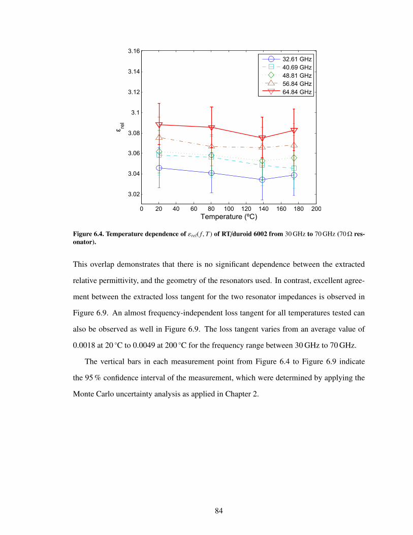
Figure 6.4. Temperature dependence of !rel( f , T ) of RT/duroid 6002 from 30 GHz to 70 GHz (70# res-onator).
This overlap demonstrates that there is no significant dependence between the extracted
relative permittivity, and the geometry of the resonators used. In contrast, excellent agree-
ment between the extracted loss tangent for the two resonator impedances is observed in
Figure 6.9. An almost frequency-independent loss tangent for all temperatures tested can
also be observed as well in Figure 6.9. The loss tangent varies from an average value of
0.0018 at 20 "C to 0.0049 at 200 "C for the frequency range between 30 GHz to 70 GHz.
The vertical bars in each measurement point from Figure 6.4 to Figure 6.9 indicate
the 95 % confidence interval of the measurement, which were determined by applying the
Monte Carlo uncertainty analysis as applied in Chapter 2.
84
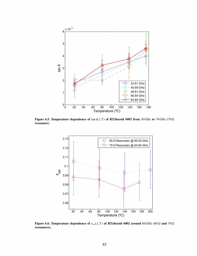
Figure 6.5. Temperature dependence of tan "( f , T ) of RT/duroid 6002 from 30 GHz to 70 GHz (70#resonator).
Figure 6.6. Temperature dependence of !rel( f , T ) of RT/duroid 6002 around 60 GHz (60# and 70#resonators).
85
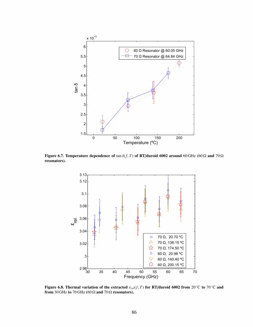
Figure 6.7. Temperature dependence of tan "( f , T ) of RT/duroid 6002 around 60 GHz (60# and 70#resonators).
Figure 6.8. Thermal variation of the extracted !rel( f , T ) for RT/duroid 6002 from 20 "C to 70 "C andfrom 30 GHz to 70 GHz (60# and 70# resonators).
86
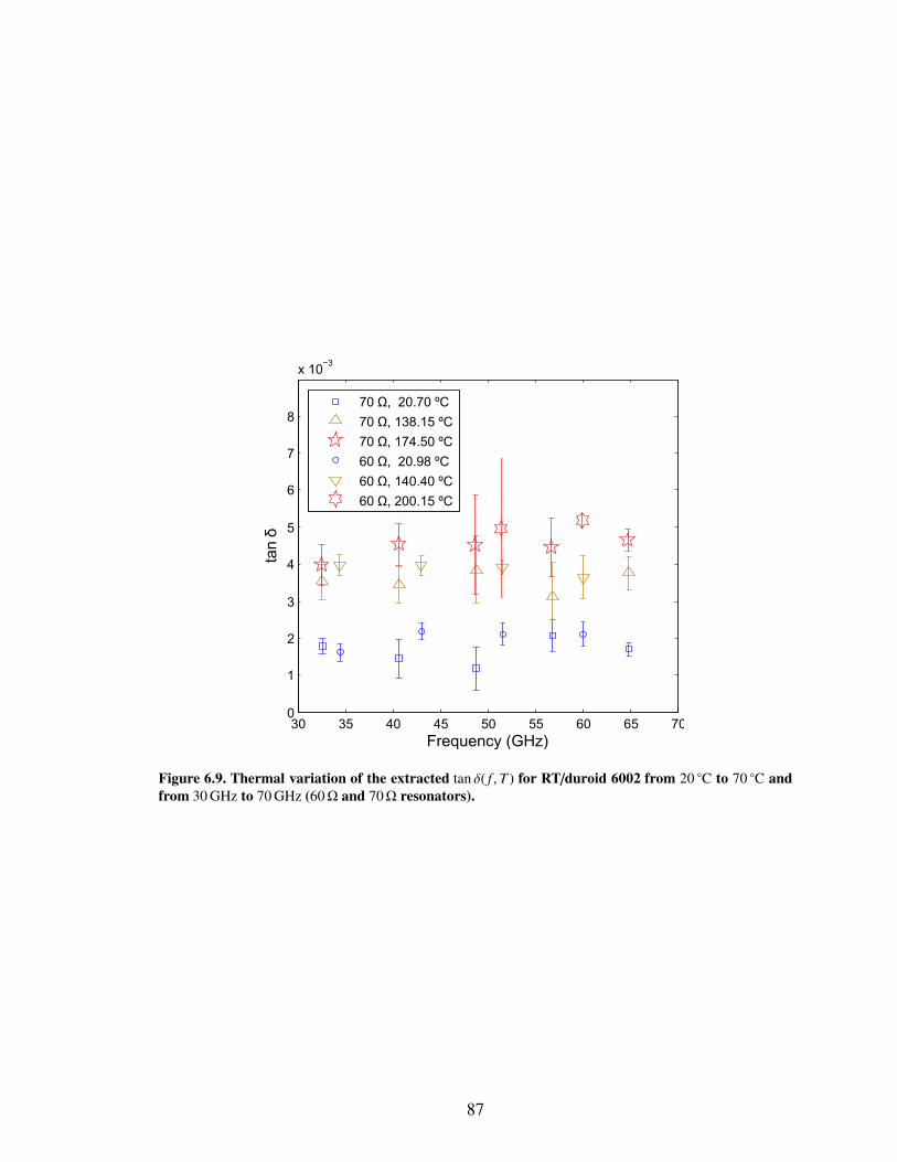
Figure 6.9. Thermal variation of the extracted tan "( f , T ) for RT/duroid 6002 from 20 "C to 70 "C andfrom 30 GHz to 70 GHz (60# and 70# resonators).
87

CHAPTER 7
COMPACT AND LOW-COST TOPOLOGY FOR
EVANESCENT-MODE WAVEGUIDE FILTERS WITH
DIELECTRIC LOADING IN THE X BAND
7.1 Inctroduction
Over the past 40 years, much of the innovation in microwave cavity filters has been fo-
cused in developing compact topologies, which enable their integration in communication
or remote sensing systems where real estate and high performance is a major concern (such
as in satellite and airborne applications). Extensive reviews of these compact topologies
are presented in [107, 108] and, among others, include the use of dielectric, dual-mode, or
evanescent-mode waveguide (EMW) resonators.
Still to this day [109], one of the major challenges in multi-pole, cavity-filter design
at microwave frequencies is to provide a compact size while maintaining a high unloaded
quality factor (Qu). A high resonator Qu is essential in filter performance because it allows
1) to reduce the insertion loss (IL, defined as $20 log(|S 21|) dB) in the pass band of the filter,
and 2) to implement sharp rejection responses. In this sense, cavity filters have allowed the
realization of filter responses with exceptional performance because of their high Qu and
high-power handling capabilities, at the cost of an increased size when compared to planar
filters.
EMW filters, thoroughly revised in [110], achieve a high Qu while keeping a compact
size by operating below the cut-o! frequency of the corresponding rectangular waveguide
(Figure 1(a)). Multi-pole operation can then be achieved by placing periodic reactive ob-
stacles in the EMW such as metallic ridges or pieces of dielectric materials, or by coupling
resonator sections through inductive irises.
The development of a three-pole filter using EMW resonators and quartz dielectric is
presented in this chapter. The dielectric loading is used to attain a compact size and an
88
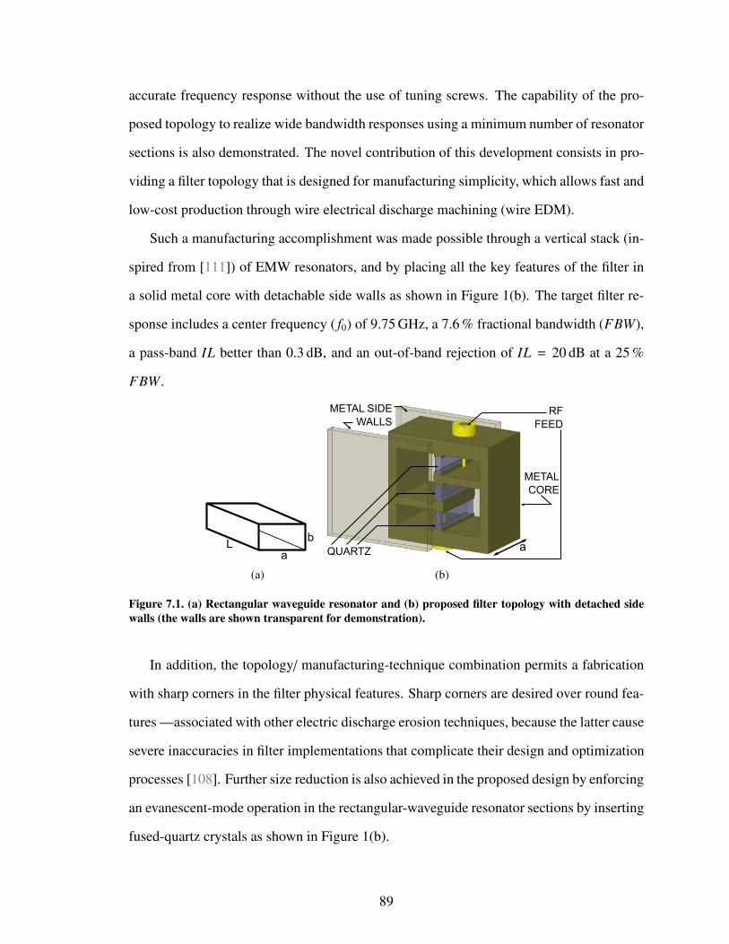
accurate frequency response without the use of tuning screws. The capability of the pro-
posed topology to realize wide bandwidth responses using a minimum number of resonator
sections is also demonstrated. The novel contribution of this development consists in pro-
viding a filter topology that is designed for manufacturing simplicity, which allows fast and
low-cost production through wire electrical discharge machining (wire EDM).
Such a manufacturing accomplishment was made possible through a vertical stack (in-
spired from [111]) of EMW resonators, and by placing all the key features of the filter in
a solid metal core with detachable side walls as shown in Figure 1(b). The target filter re-
sponse includes a center frequency ( f0) of 9.75 GHz, a 7.6 % fractional bandwidth (FBW),
a pass-band IL better than 0.3 dB, and an out-of-band rejection of IL = 20 dB at a 25 %
FBW.
(a)
(b)
Figure 7.1. (a) Rectangular waveguide resonator and (b) proposed filter topology with detached sidewalls (the walls are shown transparent for demonstration).
In addition, the topology/ manufacturing-technique combination permits a fabrication
with sharp corners in the filter physical features. Sharp corners are desired over round fea-
tures —associated with other electric discharge erosion techniques, because the latter cause
severe inaccuracies in filter implementations that complicate their design and optimization
processes [108]. Further size reduction is also achieved in the proposed design by enforcing
an evanescent-mode operation in the rectangular-waveguide resonator sections by inserting
fused-quartz crystals as shown in Figure 1(b).
89
This chapter is organized as follows: a new figure of merit (FoM) to compare the
performance and compactness of other cavity bandpass filters to the proposed topology
is introduced in Section 7.2; the filter design process is covered in Section 7.3; and the
performance of the implemented prototype in brass is presented in Section 7.4.
7.2 A New FoM for Cavity Filters
It is desired that the new FoM is capable of comparing filters with di!erent sizes and form
factors, both a!ected by parameters such as f0, filtering function, and measured insertion
loss in the pass band. Thus, the proposed filter FoM is defined as:
FoM = |ILmin| ·:GV · FBW
;$1, (7.1)
where GV = Vm f g/(n · Videal) and is a compactness factor that normalizes the volume of the
manufactured filter (Vm f g) relative to the volume occupied by n propagating-mode and air-
filled cavity resonators with thin walls and volume Videal. The parameter n is the order of
the filter under analysis. The insertion loss (ILmin) in the pass band in dB is also included
and is defined as |ILmin| = 10$ILmin/20, and represents an indirect measure of the resonators
Qu achieved in the filter implementation.
The quantity Vm f g is defined as the volume of the manufactured filter excluding feed
connectors, but including the thickness of the enclosing walls. On the other hand, Videal is
obtained, for the specific case of rectangular resonators, by assigning a rectangular waveg-
uide “a” dimension corresponding to the cut-o! wavelength of the lowest frequency of the
filter pass band ( flo); a height of the cavity “b” equal to the height of a single manufactured
resonator or enclosing waveguide of the filter under analysis; and L is calculated for a T E10
resonance at f0.
The following assertions can be made about the proposed filter FoM: 1) a high FoM
represents a compact and low-loss filter; 2) a Vm f g > Videal results in a low FoM because
no relative size reduction is achieved; 3) since the measure of compactness given by GV is
relative, it is possible that small filters have a low FoM if Vm f g > Videal; and 4) narrow-band
90

filters with a small FBW will tend to have a high FoM as long as they have a low loss and
considerable size reduction.
For instance, the three-pole filter reported in [111] has a Vm f g = 2.574 cm3, a GV = 1.43
and a measured IL = 2.0 dB for a FoM = 15. In this case, the low FoM is due to a high
insertion loss in the pass band and achieves no relative size reduction. Likewise, for the
three-pole, dielectric-resonator filter recently presented in [109], a FoM = 36 is obtained
because size reduction is achieved (GV = 0.71) and because of its low loss and narrow
bandwidth (FBW = 3.6 %).
7.3 Design Procedure
Considering the target filter response (Section 7.1) and assuming a bandpass ripple ampli-
tude Lar = 0.1 dB, the desired filter response can be achieved using three cavity resonators
from a Chebyshev filter-order calculation [112]. The normalized coupling matrix [m] and
normalized external quality factors (rin and rout) are then determined from the low-pass and
lossless Chebyshev prototype [113] as follows:
[m] =
())))))))))))))))))*
0 0.919 0
0.919 0 0.919
0 0.919 0
/0000000000000000001
, rin = rout = 0.969 (7.2)
It is also desired to determine the required resonator Qu for the target pass-band IL. An
initial approximation for its value can be obtained from the following relation [111, 112]:
Qu = 8.686 · Cn · [FBW · ($La)0]$1 , (7.3)
where Cn = 1.6 and is determined graphically from [112] for a three-pole filter with the
specified Lar. ($La)0 is the change in IL at f0 caused by a finite value of Qu. With the
specified Lar, ($La)0 = 0.15 dB is set such that Lar + $La = 0.25 dB, which is slightly less
than the target IL at the pass band. By substituting these values in (7.3), it follows that the
manufactured resonators must have a Qu ' 1219 to meet the IL specification.
91
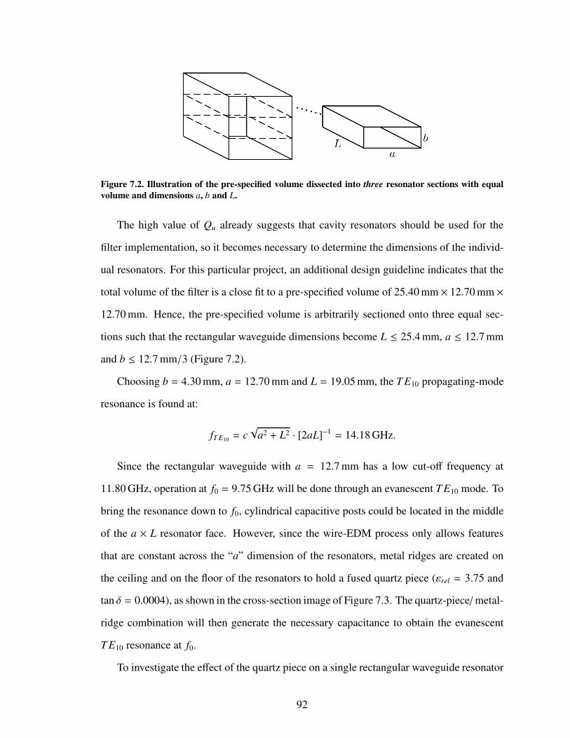
Figure 7.2. Illustration of the pre-specified volume dissected into three resonator sections with equalvolume and dimensions a, b and L.
The high value of Qu already suggests that cavity resonators should be used for the
filter implementation, so it becomes necessary to determine the dimensions of the individ-
ual resonators. For this particular project, an additional design guideline indicates that the
total volume of the filter is a close fit to a pre-specified volume of 25.40 mm # 12.70 mm #
12.70 mm. Hence, the pre-specified volume is arbitrarily sectioned onto three equal sec-
tions such that the rectangular waveguide dimensions become L & 25.4 mm, a & 12.7 mm
and b & 12.7 mm/3 (Figure 7.2).
Choosing b = 4.30 mm, a = 12.70 mm and L = 19.05 mm, the T E10 propagating-mode
resonance is found at:
fT E10= c(
a2 + L2 · [2aL]$1 = 14.18 GHz.
Since the rectangular waveguide with a = 12.7 mm has a low cut-o! frequency at
11.80 GHz, operation at f0 = 9.75 GHz will be done through an evanescent T E10 mode. To
bring the resonance down to f0, cylindrical capacitive posts could be located in the middle
of the a # L resonator face. However, since the wire-EDM process only allows features
that are constant across the “a” dimension of the resonators, metal ridges are created on
the ceiling and on the floor of the resonators to hold a fused quartz piece (!rel = 3.75 and
tan " = 0.0004), as shown in the cross-section image of Figure 7.3. The quartz-piece/metal-
ridge combination will then generate the necessary capacitance to obtain the evanescent
T E10 resonance at f0.
To investigate the e!ect of the quartz piece on a single rectangular waveguide resonator
92

Figure 7.3. Simulated e!ect of Wqtz over f0 and Qu of the T E10 evanescent mode of a single-resonator.
(now an EMW resonator), an eigen-mode simulation is performed in [51] for various sizes
of the quartz piece (Figure 7.3). The purpose of these simulations is to study the achievable
Qu at f0 in a single unloaded resonator.
While studying how f0 resonances can be obtained with several sizes of Vqtz, it was
found that Qu increases with an increase in the height of the quartz piece (hqtz), as for small
values of hqtz, the capacitance is mainly generated by larger metal ridges, which increase
the conductor losses in the cavity.
The e!ect of increasing the quartz thickness (Wqtz) on Qu and on f0 in a single resonator
with no external coupling is shown in Figure 7.3 for hqtz = 3.54 mm and a depth dimension
equal to the “a” dimension of the cavity. For Wqtz * 115 µm the unloaded f0 = 9.75 GHz
with a corresponding Qu * 1575, using brass as the material of the cavity.
Having optimized the initial dimensions of the EMW resonator for the desired Qu and
f0 values, the inter-resonator couplings study and the final filter response optimization can
begin using the coupling analysis from [114]. For the specified FBW and f0, the inter-
resonator coupling coe"cients are K12 = K21 = K23 = K32 = 0.0698 with an input-output
(I/O) coupling Qext1 = Qext2 = 3.59. The inter-resonator coupling study was realized
through simulations using [51], by coupling two resonators through an iris aperture of
93

Figure 7.4. Simulated inter-resonator coupling study: (a) S 21 response for weak RF feed coupling, (b)extracted coupling coe"cient relation to Liris, and (c) cross-section view of the electromagnetic modelused.
length Liris and by using a weakly-coupled coaxial RF Feed. The results of these simula-
tions are shown in Figure 7.4. Liris has to be extended to almost half of the floor/ ceiling
boundaries of each resonator to achieve the desired coupling coe"cient, as shown in Fig-
ure 7.4(b) and Figure 7.4(c).
Finally, the I/O coupling is realized using a coaxial transmission line with an extended
signal-conductor probe to provide the excitation of the evanescent mode. The location and
extension of this I/O probe are determined by performing group-delay simulations on a
singly-loaded resonator. Besides optimizing these two parameters, extra adjustments can
be performed by varying Wqtz as shown in Figure 7.5. As in the case of the inter-resonator
coupling, a strong I/O coupling is required, which yields to a probe location as close as
possible to the center of the a # L face. For a Qext = 13.59, the group delay at the center
94
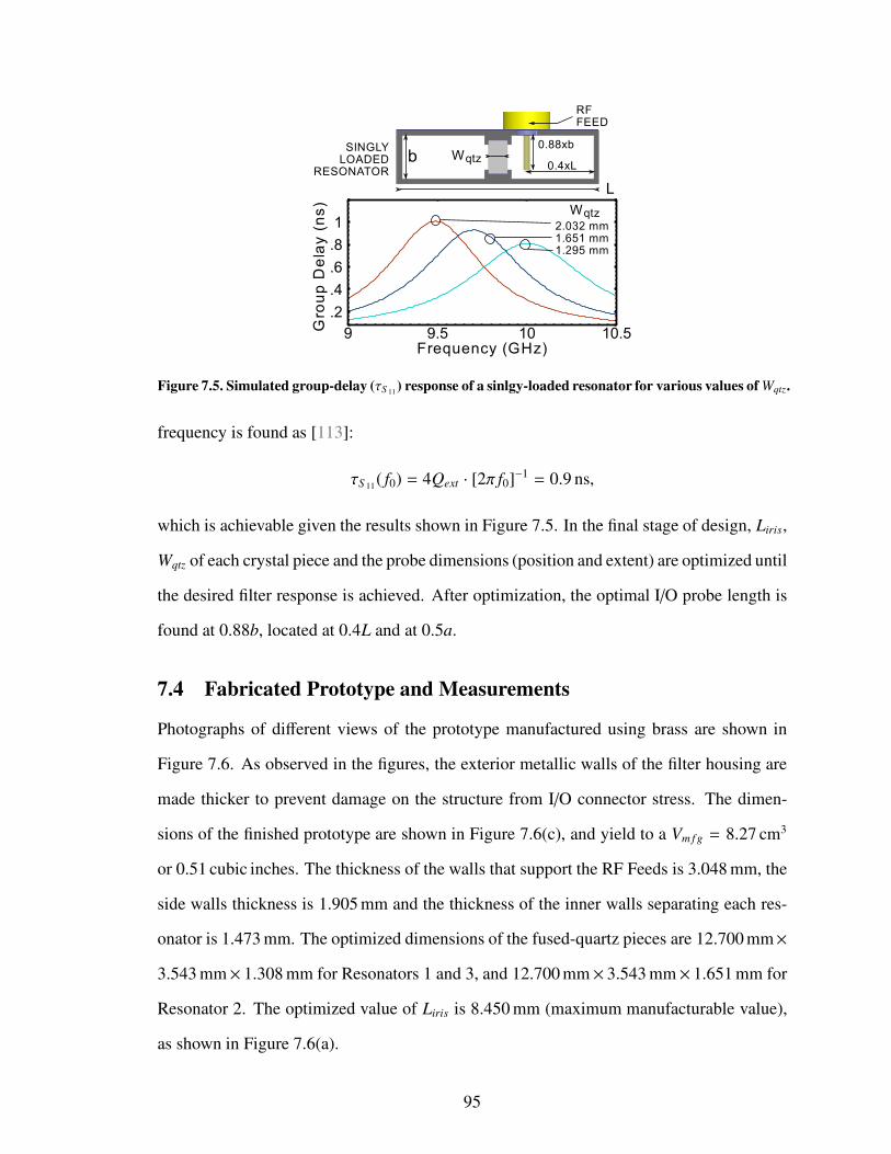
Figure 7.5. Simulated group-delay (#S 11) response of a sinlgy-loaded resonator for various values of Wqtz.
frequency is found as [113]:
#S 11( f0) = 4Qext · [2% f0]$1 = 0.9 ns,
which is achievable given the results shown in Figure 7.5. In the final stage of design, Liris,
Wqtz of each crystal piece and the probe dimensions (position and extent) are optimized until
the desired filter response is achieved. After optimization, the optimal I/O probe length is
found at 0.88b, located at 0.4L and at 0.5a.
7.4 Fabricated Prototype and Measurements
Photographs of di!erent views of the prototype manufactured using brass are shown in
Figure 7.6. As observed in the figures, the exterior metallic walls of the filter housing are
made thicker to prevent damage on the structure from I/O connector stress. The dimen-
sions of the finished prototype are shown in Figure 7.6(c), and yield to a Vm f g = 8.27 cm3
or 0.51 cubic inches. The thickness of the walls that support the RF Feeds is 3.048 mm, the
side walls thickness is 1.905 mm and the thickness of the inner walls separating each res-
onator is 1.473 mm. The optimized dimensions of the fused-quartz pieces are 12.700 mm#
3.543 mm# 1.308 mm for Resonators 1 and 3, and 12.700 mm# 3.543 mm# 1.651 mm for
Resonator 2. The optimized value of Liris is 8.450 mm (maximum manufacturable value),
as shown in Figure 7.6(a).
95
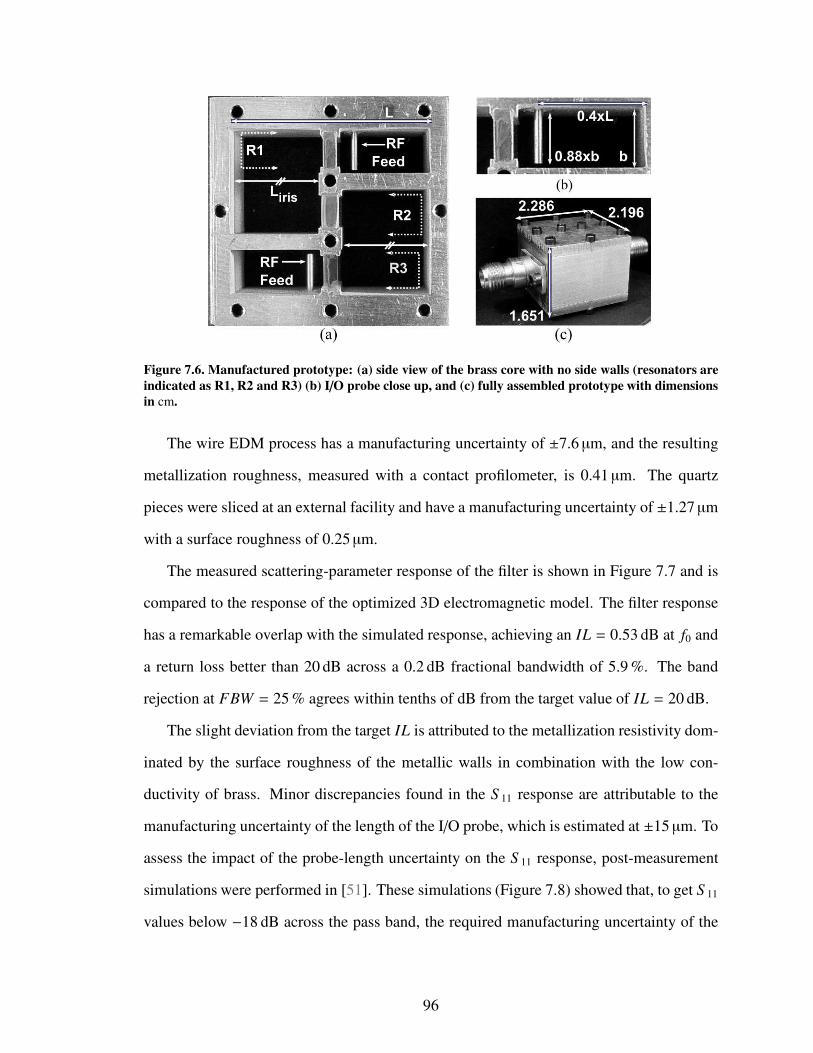
Figure 7.6. Manufactured prototype: (a) side view of the brass core with no side walls (resonators areindicated as R1, R2 and R3) (b) I/O probe close up, and (c) fully assembled prototype with dimensionsin cm.
The wire EDM process has a manufacturing uncertainty of ±7.6 µm, and the resulting
metallization roughness, measured with a contact profilometer, is 0.41 µm. The quartz
pieces were sliced at an external facility and have a manufacturing uncertainty of ±1.27 µm
with a surface roughness of 0.25µm.
The measured scattering-parameter response of the filter is shown in Figure 7.7 and is
compared to the response of the optimized 3D electromagnetic model. The filter response
has a remarkable overlap with the simulated response, achieving an IL = 0.53 dB at f0 and
a return loss better than 20 dB across a 0.2 dB fractional bandwidth of 5.9 %. The band
rejection at FBW = 25 % agrees within tenths of dB from the target value of IL = 20 dB.
The slight deviation from the target IL is attributed to the metallization resistivity dom-
inated by the surface roughness of the metallic walls in combination with the low con-
ductivity of brass. Minor discrepancies found in the S 11 response are attributable to the
manufacturing uncertainty of the length of the I/O probe, which is estimated at ±15 µm. To
assess the impact of the probe-length uncertainty on the S 11 response, post-measurement
simulations were performed in [51]. These simulations (Figure 7.8) showed that, to get S 11
values below $18 dB across the pass band, the required manufacturing uncertainty of the
96

Figure 7.7. Scattering-parameter response: simulation and measurement.
Figure 7.8. Simulated change in S 11 with I/O probe length variations within ±20 µm around the optimalvalue.
probe length should be within ±20 µm.
With an IL = 0.53 dB and having achieved a size reduction of V = 0.64, the proposed
filter has an FoM = 25. This FoM is competitive with respect to other three-pole filters in
the X Band (Table 7.1), considering the fact that the dielectric resonator filter in [109] has
a more intricate manufacturing process and that its bandpass ripple is as high as 0.5 dB.
97

Table 7.1. Summary of filter FoM calculations for various three-pole filters in the X band.
Harle et al. [111] Kazemi et al. [109] This Work
Vm f g cm3) 2.57 25.74 8.29
Videal (cm3) 1.79 36.08 13.05
V (%) 144 71 64
a (cm) 1.52 1.70 1.58
b (cm) 0.05 0.80 0.43
L (cm) 7.82 8.82 6.38
IL (cm) 2.00 0.50 0.53
FBW (%) 3.7 3.6 5.9
flo (GHz) 9.82 8.80 9.46
f0 (GHz) 10.01 8.96 9.75
FoM 14.9 36.5 25.1
98

CHAPTER 8
CONCLUSION
(...) a man can be given only what he can use; and he can use
only that for which he has sacrificed something.
Strange Life of Ivan Osokin, 1947
P.D. Ouspensky
A broad range of designs, experiments and ideas that increase the understanding of
lightweight front end components and systems for radar applications were presented in this
thesis. For instance, the development of an ultra-thin organic antenna array technology was
successfully demonstrated in Chapters 3, 4 and 5, showing that it is possible to achieve a
high-power operation in a thin organic package without the need of bulky thermal manage-
ment solutions.
The experience in the development of this antenna array technology, lead to the study
of the thermal limitations of various thin-film materials of interest, which included ceram-
ics and organic dielectrics. Theoretical calculations revealed that microstrip architectures
implemented in commercial LCP packages should not be operated beyond 150 W to avoid
reaching the melting temperature of the dielectric. As an alternative to liquid polymers,
PTFE/ ceramic hybrid materials such as RT/duroid 6002 showed promising thermal prop-
erties, not only in terms of a higher thermal conductivity than that of LCP, but also on the
thermal stability of the dielectric properties over a wide temperature and frequency range
as it was demonstrated in Chapter 6. Theoretical calculations showed that microstrip
lines implemented on commercial laminates of RT/duroid 6002 (with KRT/duroid 6002 =
0.6 W m$1 "C$1, which is three times KLCP), could support up to 300 W with no additional
thermal management solutions.
To take advantage of the low-cost organic packages and to overcome their thermal limi-
tations, it is possible to have multiple arrays (such as the one presented in Chapter 5) fed by
99

compact components capable of handling high power levels. These components could be
implemented in more expensive technologies such as thin-film circuits on aluminum nitride
(Appendix A), or bulkier yet in compact waveguide circuits, such as the evanescent-mode
cavity filter presented in Chapter 7.
In the following sections, the contributions made in this work are summarized, along
with potential research paths that could expand the work presented in this thesis.
8.1 List of Contributions
1. For the first time, the dielectric properites of the thin-film, organic substrates RT/duroidR!
5880, 6002 and 6202 were measured from 30 GHz to 70 GHz, covering most of the
Ka and V radar bands.
2. For the first time, the dielectric properties of RT/duroid 6002 were characterized over
temperature (20 "C to 175 "C) and over frequency (30 GHz to 70 GHz). RT/duroid
6002 showed exhibited a very stable behavior over temperature and frequency, which
makes it a promising candidate for high-power and lightweight radar applications.
3. For the first time, an uncertainty assessment was applied to the microstrip ring res-
onator method for material characterization using the Monte Carlo uncertainty analy-
sis. The metrological uncertainty analysis took into account the measurement uncer-
tainty of the physical features of the resonators and the substrates (resonator radius,
microstrip width, substrate thickness and surface roughness) and the uncertainty of
the network analyzer. This analysis was successfully applied to the thermal charac-
terization of RT/duroid 6002, which was also done for the first time.
4. For the first time, the operation of an organic T/R phased array was demonstrated
using MEMs and SiGe active devices. The contribution in this work consisted in the
modeling and design of the active circuit interconnects, the assembly and characteri-
zation of the system.
100

5. Low profile interconnects were successfully designed, modeled and implemented
for ultra-thin organic phased arrays. Particular emphasis was placed in the modeling
and characterization of stripline beam-former network technology, and its integration
with microstrip and coplanar interconnects.
6. To the best of the author’s knowledge, the active antenna array with the highest EIRP
was demonstrated in the thinnest organic package using the largest number of flip-
chip bonded SiGe ICs. The high-power operation was achieved by developing an in-
novative packaging architecture implemented on a multi-layer, hybrid substrate stack
of LCP and RT/duroid 5880 LZ. The active array was able to achieve 47 dBm with-
out thermal management since multiple low-power ICs were deployed throughout
the antenna board.
7. A new figure of merit was introduced to allow the comparison of microwave cavity
filters. The figure of merit allows the comparison of filters operating at di!erent
compactness factors, center frequencies, operation bandwidths and levels of insertion
loss.
8. A new, low-cost and compact topology was introduced for cavity filters in the X
band. On one hand, cost reduction was achieved by simplifying the manufacturing
process using a single-cut setup with wire electric-discharge machining to create the
main features of the filter. On the other hand, compact size was achieved by using an
evanescent-mode topology with dielectric quartz loading.
101

8.2 Future Work
1. Future research on lightweight phased array technologies on organic substrates should
focus in increasing further the EIRP while maintaining a low profile package. To this
end, besides improving the e"ciency of beam-former networks, the priority should
be set to increasing the output power of the SiGe Modules or in using more e"cient
technologies such as is the case of GaN devices. Thus, the design and implemen-
tation of modules with multiple GaN PA’s could be pursued to fully understand the
capability of organic packages while performing on high-power conditions.
2. Although Bahl’s electrothermal analysis gives a good first approximation to the ther-
mal modeling of microstrip interconnects, his thermal model requires further valida-
tion through full 3D electromagnetic heating models using multi-physics simulation
tools that are based on the method of moments. One challenge that needs to be ad-
dressed is to formulate the proper boundary conditions that reflect the real behavior of
microstrip packages. This can be achieved experimentally by measuring the temper-
ature of the packages over time for di!erent input-power levels on simple microstrip
lines. In turn, the boundary conditions of the models should be adjusted so that the
simulation results matches the thermal behavior of simple interconnects. With proper
boundary conditions defined and validated with measurement, the electromagnetic
heating models could be used to model complex systems such as high-power active
modules, beam-former networks and fully functional Tx phased arrays.
3. Innovative heat dissipation schemes using micro-channel cooling [97] implemented
in organic substrates such as the ones proposed by Oshman et al. [98–100] should be
explored in the microwave regime. These technologies should be integrated in high-
frequency phased array modules to increase the thermal e"ciency under high-power
conditions. Hence, further research on flexible high-power modules should integrate
102
the expertise from disciplines outside of RF engineering such as Mechanical Engi-
neering (to incorporate thermal aspects) and Material Science (to develop innovative
micro-fabrication techniques on novel flexible materials).
4. Further research on organic-substrate packages should also include the thermal char-
acterization of a broader variety of dielectric substrates. The substrates should be
chosen according to light weight, hermeticity, broadband stability of dielectric prop-
erties, low RF loss and high thermal conductivity. The #!reland #tan " should be deter-
mined and incorporated in multiphysics electrothermal models. The thorough mod-
eling of temperature-dependent properties of these systems is necessary to increase
the e"cacy of the 3D models.
103

8.3 List of Publications and Academic Achievements8.3.1 Awards
1. First place in student paper competition of the 2012 IEEE Radio and Wireless Sym-
posium (RWS), Santa Clara, California.
8.3.2 Invention Disclosures1. C. A. Donado Morcillo, B. Lacroix, H. Gu, J. Miller and J. Papapolymerou, “Dielectric-
loaded, Evanescent-Mode Cavity Filter in the X Band with Compact Size and Re-duced Manufacturing Complexity”, United States Patent and Trademark O!ce (USPTO),provisional patent No. 61/623,692, filed April 13, 2012.
8.3.3 Journal Articles1. C. A. Donado Morcillo and J. Papapolymerou, “Uncertainty Assessment of the
Microstrip Ring Resonator Method for Dielectric Material Characterization,” Mi-
crowave Theory and Techniques, IEEE Transactions on, in preparation, 2013.
2. C. A. Donado Morcillo, C. E. Patterson, B. Lacroix, C. Coen, C. H. J. Poh, J. D.Cressler, and J. Papapolymerou, “An Ultra-Thin, High-power, and Multilayer Or-ganic Antenna Array With T/R Functionality in the X-band,” Microwave Theory and
Techniques, IEEE Transactions on, no. 99, pp. 1-12, Dec. 2012 (early access).
3. S. Courreges, C. A. Donado Morcillo, S. Bhattacharya, and J. Papapolymerou,
“Reduced-size multilayer X-band filters with stacked resonators on a flexible organicsubstrate,” IET Microwaves, Antennas & Propagation, vol. 4, no. 2, pp. 277285,
2010.
8.3.4 Conference Papers
1. S. Pavlidis, C. A. Donado Morcillo, P. Song, W. T. Khan, R. Fitch, J. Gillespie, R.Febo, T. Quach and J. Papapolymerou,“A Hybrid GaN/Organic X-Band TransmitterModule”, accepted for publication in Radio and Wireless Symposium (RWS), 2013
IEEE.
2. C. A. Donado Morcillo, B. Lacroix, H. Gu, J. Miller and J. Papapolymerou, “Com-
pact and Low-cost Topology for Evanescent-Mode Waveguide Filters with Dielec-tric Loading in the X Band,” in Microwave Conference, 2012. 42nd European, Oct.
2012.
3. C. A. Donado Morcillo, C. Patterson, and J. Papapolymerou, Design of stripline
beam-former network components for low-profile, organic phased arrays in the Xband, in Radio and Wireless Symposium (RWS), 2012 IEEE, Jan. 2012, pp. 179-182.
104

4. C. A. Donado Morcillo, C. Patterson, T. Thrivikraman, B. Lacroix, B. Wilson, B.Hudson, C. Coen, C. Poh, T. Heath, J. Cressler, and J. Papapolymerou, “A lightweight,64-element, organic phased array with integrated transmit-receive sige circuitry in the
X band,” in Microwave Symposium Digest (MTT), 2011 IEEE MTT-S International,June 2011, pp. 1-4.
5. C. A. Donado Morcillo, S. K. Bhattacharya, A. Horn, and J. Papapolymerou, “Con-ductor surface-roughness e!ect in the loss tangent measurement of low-loss organicsubstrates from 30 GHz to 70 GHz,” in Proc. 60th Electronic Components and Tech-
nology Conf. (ECTC), 2010, pp. 727-734.
6. C. A. Donado Morcillo, S. K. Bhattacharya, A. Horn, and J. Papapolymerou, “Ther-mal stability of the dielectric properties of the low-loss, organic material RT/duroid
6002 from 30 GHz to 70 GHz,” in Proc. 60th Electronic Components and Technology
Conf. (ECTC), 2010, pp. 1830-1833.
7. A. L. V. Lopez, S. K. Bhattacharya, C. A. D. Morcillo, J. Papapolymerou, and D.Choudhury, “Novel low loss thin film materials for wireless 60 GHz application,”in Proc. 60th Electronic Components and Technology Conf. (ECTC), 2010, pp.
19901995.
105

APPENDIX A
DESIGN OF WILKINSON POWER DIVIDERS ON ALUMINUM
NITRIDE WITH TANTALUM NITRIDE RESISTORS
The design of a two-way WPD with an equal power split (1:1) was first introduced by
Wilkinson in 1960 [115] and it’s schematic is shown in Figure A.1. The WPD provides
an impedance match at all ports and excellent levels of isolation between the output ports,
given that these ports are matched to the output impedance.
Figure A.1. Schematic diagram of a two-way WPD with equal power split.
The line impedances shown in Figure A.1 are obtained for an equal power split at ports
2 and 3 with the following relations [62]:
Z =(
2Z0 = Z02 = Z03, (A.1)
R = 2Z0, (A.2)
where Z02 and Z03 are the characteristic impedances of the $/4 adapters of Figure A.1, and
R is the value of the isolation resistor. For a general case, it is possible to design a WPD
with an unequal power split between ports 2 and 3 (Figure A.2), with a “port three power”
P3 to “port two power” P2 ratio of K2 as follows [62]:
K2 = P3/P2 (A.3)
Z03 = Z0
H1 + K2
K3, (A.4)
Z02 = K2Z03 = Z0
2K(1 + K2), (A.5)
RK = Z0
+K +
1
K
,. (A.6)
106
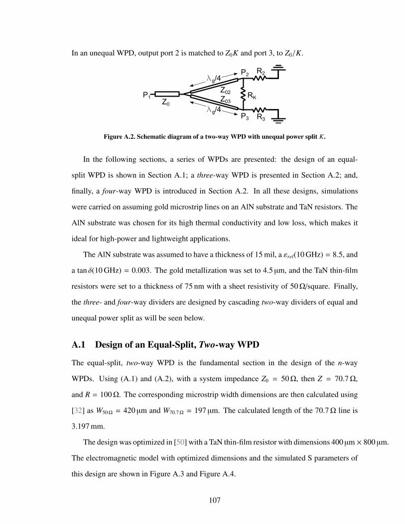
In an unequal WPD, output port 2 is matched to Z0K and port 3, to Z0/K.
Figure A.2. Schematic diagram of a two-way WPD with unequal power split K.
In the following sections, a series of WPDs are presented: the design of an equal-
split WPD is shown in Section A.1; a three-way WPD is presented in Section A.2; and,
finally, a four-way WPD is introduced in Section A.2. In all these designs, simulations
were carried on assuming gold microstrip lines on an AlN substrate and TaN resistors. The
AlN substrate was chosen for its high thermal conductivity and low loss, which makes it
ideal for high-power and lightweight applications.
The AlN substrate was assumed to have a thickness of 15 mil, a !rel(10 GHz) = 8.5, and
a tan "(10 GHz) = 0.003. The gold metallization was set to 4.5 µm, and the TaN thin-film
resistors were set to a thickness of 75 nm with a sheet resistivity of 50#/square. Finally,
the three- and four-way dividers are designed by cascading two-way dividers of equal and
unequal power split as will be seen below.
A.1 Design of an Equal-Split, Two-way WPD
The equal-split, two-way WPD is the fundamental section in the design of the n-way
WPDs. Using (A.1) and (A.2), with a system impedance Z0 = 50#, then Z = 70.7#,
and R = 100#. The corresponding microstrip width dimensions are then calculated using
[32] as W50# = 420 µm and W70.7# = 197 µm. The calculated length of the 70.7# line is
3.197 mm.
The design was optimized in [50] with a TaN thin-film resistor with dimensions 400 µm # 800 µm.
The electromagnetic model with optimized dimensions and the simulated S parameters of
this design are shown in Figure A.3 and Figure A.4.
107

Figure A.3. Optimized electromagnetic model of the two-way WPD.
Figure A.4. Simulated S-Parameters of the two-way WPD.
A.2 Design of a Three-way WPD
The design of equal-split n-way WPDs using thin-film technology is not a trivial task when
n > 2. The fundamental issue is that the isolation resistors require three-dimensional (3D)
interconnects to provide a common point of connection between them, which is di"cult
to implement using thin-film technology. To overcome this issue, the approach of this
section involves the design of a three-way WPD by cascading an unequal WPD with a
1/3:2/3 power split ratio (1:2 WPD), with an two-way equal-split WPD on the 2/3 branch,
as shown in Figure A.5.
With K2 = 0.5, then Z02 = 51.49#, Z03 = 102.99#, R2 = 35.36# and R3 = 70.71#.
The isolation resistance is calculated as RK = 106.07# and the TaN resistor dimensions
are then calculated at 400 µm # 848.53 µm.
Since the output-port impedances are at a mismatch with respect to Z0, $g/4 adapters
are deployed at the outputs of the 1:2 WPD to provide the required match. The adapter
at the 2/3 output has an impedance Z$g/4,2/3 =(
Z02Z0 = 42.04#, and the one at the 1/3
output, Z$g/4,1/3 =(
Z03Z0 = 59.46#. The calculated widths of the microstrip lines used in
108

Figure A.5. Schematic diagram of the proposed three-way WPD.
Table A.1. Summary of dimensions for the microstrip lines used in the three-way WPD
Impedance section Impedance value (#) Microstrip width (µm) $g/4 length (mm)
Z02 51.5 405 3.100
Z03 103.0 63 3.308
Z$g/4,2/3 42.0 582 3.037
Z$g/4,1/3 59.5 290 3.145
Z 70.7 197 3.197
Z0 50 420 –
this design are summarized in Table A.1.
The optimized electromagnetic model of the three-way WPD is shown in Figure A.6
and its corresponding S-parameter response is shown in Figure A.7.
Figure A.6. Optimized electromagnetic model of the three-way WPD.
109
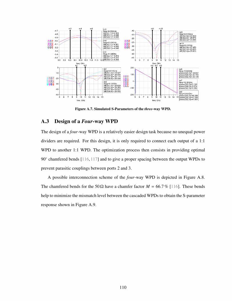
Figure A.7. Simulated S-Parameters of the three-way WPD.
A.3 Design of a Four-way WPD
The design of a four-way WPD is a relatively easier design task because no unequal power
dividers are required. For this design, it is only required to connect each output of a 1:1
WPD to another 1:1 WPD. The optimization process then consists in providing optimal
90" chamfered bends [116, 117] and to give a proper spacing between the output WPDs to
prevent parasitic couplings between ports 2 and 3.
A possible interconnection scheme of the four-way WPD is depicted in Figure A.8.
The chamfered bends for the 50# have a chamfer factor M = 66.7 % [116]. These bends
help to minimize the mismatch level between the cascaded WPDs to obtain the S-parameter
response shown in Figure A.9.
110

Figure A.8. Optimized electromagnetic model of the four-way WPD.
Figure A.9. Simulated S-Parameters of the four-way WPD.
111
REFERENCES
[1] M. I. Skolnik, Introduction to radar systems. Boston: McGraw Hill, 3rd ed., 2001.
[2] “IEEE Standard Letter Designations for Radar-Frequency Bands,” IEEE Std 521-
2002 (Revision of IEEE Std 521-1984), pp. 1–3, 2003.
[3] B. Fleming, “Recent advancement in automotive radar systems [automotive elec-tronics],” Vehicular Technology Magazine, IEEE, vol. 7, pp. 4 –9, Mar. 2012.
[4] J. Paden, D. Braaten, and P. Gogineni, “Beneath the ice sheets,” Spectrum, IEEE,vol. 48, pp. 36 –42, Sep. 2011.
[5] S. Yueh, S. Dinardo, A. Akgiray, R. West, D. Cline, and K. Elder, “Airborne ku-bandpolarimetric radar remote sensing of terrestrial snow cover,” Geoscience and Remote
Sensing, IEEE Transactions on, vol. 47, pp. 3347 –3364, Oct. 2009.
[6] H. Rott, S. Yueh, D. Cline, C. Duguay, R. Essery, C. Haas, F. He andlie an-dre, M. Kern, G. Macelloni, E. Malnes, T. Nagler, J. Pulliainen, H. Rebhan, andA. Thompson, “Cold regions hydrology high-resolution observatory for snow and
cold land processes,” Proceedings of the IEEE, vol. 98, pp. 752 –765, May 2010.
[7] M. Swaminathan, V. Sundaram, J. Papapolymerou, and P. Raj, “Polymers for rf
apps,” Microwave Magazine, IEEE, vol. 12, pp. 62 –77, Dec. 2011.
[8] R. Corporation, “Rogers Corporation Product Catalog.” [Available online] http://www.rogerscorp.com/products/, Aug. 2012.
[9] D. Thompson, O. Tantot, H. Jallageas, G. Ponchak, M. Tentzeris, and J. Papapoly-merou, “Characterization of liquid crystal polymer (LCP) material and transmission
lines on LCP substrates from 30 to 110 GHz,” Microwave Theory and Techniques,
IEEE Transactions on, vol. 52, pp. 1343 – 1352, Apr. 2004.
[10] C. Patterson, S. Bhattacharya, J. Zepess, S. Leiphart, W. Trueheart, J. Ajoian,
Z. Co!man, and J. Papapolymerou, “A 7.45 ghz baw filter on a 3d low cost organicpackage,” in Microwave Symposium Digest (MTT), 2011 IEEE MTT-S International,pp. 1 –4, June 2011.
[11] R. Bairavasubramanian, S. Pinel, J. Papapolymerou, J. Laskar, C. Quendo, E. Rius,A. Manchec, and C. Person, “Dual-band filters for wlan applications on liquid crystal
polymer technology,” in Microwave Symposium Digest, 2005 IEEE MTT-S Interna-
tional, p. 4, June 2005.
112
[12] C. E. Patterson, D. Dawn, and J. Papapolymerou, “A W-band CMOS PA encapsu-lated in an organic flip-chip package,” in Microwave Symposium Digest (MTT), 2012
IEEE MTT-S International, pp. 1 –3, June 2012.
[13] P. Rice, M. Black, D. Li, J. Yip, and J. McNicol, “Development of a low cost 94 GHzimaging receiver using multilayer liquid crystal polymer technology,” in Physics and
Engineering of Microwaves, Millimeter and Submillimeter Waves (MSMW), 2010
International Kharkov Symposium on, p. 1, June 2010.
[14] A. Amadjikpe and, D. Choudhury, G. Ponchak, and J. Papapolymerou, “Highly di-
rective package-integrated dipole arrays for low-cost 60-GHz front end modules,”in Microwave Symposium Digest (MTT), 2010 IEEE MTT-S International, pp. 348–351, May 2010.
[15] D. Thompson, M. Tentzeris, and J. Papapolymerou, “Packaging of mmics in multi-layer lcp substrates,” Microwave and Wireless Components Letters, IEEE, vol. 16,
pp. 410 –412, July 2006.
[16] C. Patterson, A. Yepes, T. Thrivikraman, S. Bhattacharya, J. Cressler, and J. Papa-polymerou, “A lightweight x-band organic antenna array with integrated sige ampli-
fier,” in Radio and Wireless Symposium (RWS), 2010 IEEE, pp. 84 –87, Jan. 2010.
[17] C. E. Patterson, T. K. Thrivikraman, S. K. Bhattacharya, C. T. Coen, J. D. Cressler,
and J. Papapolymerou, “Development of a multilayer organic packaging techniquefor a fully embedded t/r module,” in Microwave Conference (EuMC), 2011 41st
European, pp. 261 –264, Oct. 2011.
[18] W. Yun, V. Sundaram, and M. Swaminathan, “High-Q Embedded Passives on LargePanel Multilayer Liquid Crystalline Polymer-Based Substrate,” Advanced Packag-
ing, IEEE Transactions on, vol. 30, pp. 580 –591, Aug. 2007.
[19] D. G. Kam, D. Liu, A. Natarajan, S. Reynolds, and B. Floyd, “Organic PackagesWith Embedded Phased-Array Antennas for 60-GHz Wireless Chipsets,” Compo-
nents, Packaging and Manufacturing Technology, IEEE Transactions on, vol. 1,pp. 1806–1814, Nov. 2011.
[20] C. Patterson, T. Thrivikraman, A. Yepes, S. Begley, S. Bhattacharya, J. Cressler, and
J. Papapolymerou, “A Lightweight Organic X-Band Active Receiving Phased ArrayWith Integrated SiGe Amplifiers and Phase Shifters,” Antennas and Propagation,
IEEE Transactions on, vol. 59, pp. 100 –109, Jan. 2011.
[21] C. Donado Morcillo, C. Patterson, T. Thrivikraman, B. Lacroix, B. Wilson, B. Hud-son, C. Coen, C. Poh, T. Heath, J. Cressler, and J. Papapolymerou, “A lightweight,
64-element, organic phased array with integrated transmit-receive sige circuitry inthe x band,” in Microwave Symposium Digest (MTT), 2011 IEEE MTT-S Interna-
tional, pp. 1 –4, June 2011.
113

[22] A. Moussessian, L. Del Castillo, J. Huang, G. Sadowy, J. Ho!man, P. Smith,T. Hatake, C. Derksen, B. Lopez, and E. Caro, “An active membrane phased ar-ray radar,” in Microwave Symposium Digest, 2005 IEEE MTT-S International, p. 4
pp., June 2005.
[23] A. Wegener, C. Fulton, J. Gregory, and W. Chappell, “Large area integration ofembedded high power rf amplifiers in a thin organic panel high power rf amplifiers
in a thin organic panel,” in Microwave Symposium Digest, 2009. MTT ’09. IEEE
MTT-S International, pp. 801 –804, June 2009.
[24] A. Valdes-Garcia, S. Nicolson, J.-W. Lai, A. Natarajan, P.-Y. Chen, S. Reynolds, J.-H. C. Zhan, D. Kam, D. Liu, and B. Floyd, “A fully integrated 16-element phased-array transmitter in sige bicmos for 60-ghz communications,” Solid-State Circuits,
IEEE Journal of, vol. 45, pp. 2757 –2773, Dec. 2010.
[25] Y. A. Atesal, B. Cetinoneri, K.-J. Koh, and G. M. Rebeiz, “X/Ku-band 8-elementphased arrays based on single silicon chips,” in Proc. IEEE MTT-S Int. Microwave
Symp. Digest (MTT), pp. 1258–1261, 2010.
[26] T. Kamgaing, E. Davies-Venn, and K. Radhakrishnan, “A compact 802.11 a/b/g/nwlan front-end module using passives embedded in a flip-chip bga organic package
substrate,” in Microwave Symposium Digest, 2009. MTT ’09. IEEE MTT-S Interna-
tional, pp. 213 –216, June 2009.
[27] K.-J. Koh and G. Rebeiz, “An x- and ku-band 8-element phased-array receiverin 0.18-sige bicmos technology,” Solid-State Circuits, IEEE Journal of, vol. 43,pp. 1360–1371, June 2008.
[28] M. Borgarino, A. Polemi, and A. Mazzanti, “Low-Cost Integrated Microwave Ra-diometer Front-End for Industrial Applications,” Microwave Theory and Techniques,
IEEE Transactions on, vol. 57, pp. 3011 –3018, Dec. 2009.
[29] J. J. Lee, “G/t and noise figure of active array antennas,” [IEEE Trans. Antennas
Propag.], vol. 41, no. 2, pp. 241–244, 1993.
[30] W. Khan, S. Bhattacharya, C. Patterson, G. Ponchak, and J. Papapolymerou, “Low
cost 60 ghz rf front end transceiver integrated on organic substrate,” in Microwave
Symposium Digest (MTT), 2011 IEEE MTT-S International, pp. 1 –4, June 2011.
[31] B. N. Taylor and C. E. Kuyatt, Guidelines for evaluating and expressing the uncer-
tainty of NIST measurement results, vol. 1297. Gaithersburg, MD: U.S. Departmentof Commerce, Technology Administration, National Institute of Standards and Tech-
nology, 1994 ed., 1994.
[32] Agilent Technologies, “Linecalc, Advanced Design System (v.2009).”
[33] J. Baker-Jarvis, M. D. Janezic, B. Riddle, C. L. Holloway, N. G. Paulter, and J. E.
Blendell, “Dielectric and conductor-loss characterization and measurements on elec-tronic packaging materials,” 2001.
114

[34] J.-M. Heinola and K. Tolsa, “Dielectric characterization of printed wiring board ma-terials using ring resonator techniques: a comparison of calculation models,” Di-
electrics and Electrical Insulation, IEEE Transactions on, vol. 13, pp. 717 –726,
Aug. 2006.
[35] Z. Gang, H. Gronqvist, J. P. Starski, and L. Johan, “Characterization of liquid crystal
polymer for high frequency system-in-a-package applications,” Advanced Packag-
ing, IEEE Transactions on, vol. 25, no. 4, pp. 503–508, 2002.
[36] H. Lung-Hwa and C. Kai, “Equivalent lumped elements G, L, C, and unloaded Q’s
of closed- and open-loop ring resonators,” Microwave Theory and Techniques, IEEE
Transactions on, vol. 50, no. 2, pp. 453–460, 2002.
[37] K. P. Latti, M. Kettunen, J. P. Strom, and P. Silventoinen, “A Review of Microstrip T-Resonator Method in Determining the Dielectric Properties of Printed Circuit BoardMaterials,” Instrumentation and Measurement, IEEE Transactions on, vol. 56, no. 5,
pp. 1845–1850, 2007.
[38] K. C. Gupta, Microstrip lines and slotlines, pp. 32, 86–95, 108. Boston: ArtechHouse, 2nd ed., 1996.
[39] A. Sutono, N. Cafaro, J. Laskar, and M. Tentzeris, “Experimental modeling, re-peatability investigation and optimization of microwave bond wire interconnects,”
Advanced Packaging, IEEE Transactions on, vol. 24, pp. 595 –603, Nov. 2001.
[40] Z. Zhang and C. Wong, “Recent advances in flip-chip underfill: materials, process,and reliability,” Advanced Packaging, IEEE Transactions on, vol. 27, pp. 515 – 524,
Aug. 2004.
[41] L.-H. Hsu, C.-W. Oh, W.-C. Wu, E. Chang, H. Zirath, C.-T. Wang, S.-P. Tsai, W.-C.
Lim, and Y.-C. Lin, “Design, fabrication, and reliability of low-cost flip-chip-on-board package for commercial applications up to 50 ghz,” Components, Packaging
and Manufacturing Technology, IEEE Transactions on, vol. 2, pp. 402 –409, Mar.
2012.
[42] National Space Administration (NASA), “Cold-land Processes Field Experiment.”[Available online] http://nsidc.org/data/clpx/, Nov. 2012.
[43] Troughton, P., “Measurement techniques in microstrip,” Electronics Letters, vol. 5,no. 2, pp. 25–26, 1969.
[44] J.-M. Heinola and J.-P. Strom, “Evaluation of dielectric properties of printed wiringboard materials by using a microstrip-ring and strip-line ring resonator methods,”Electrical Insulation Magazine, IEEE, vol. 23, pp. 23 –29, May-June 2007.
[45] Y. Wu and F. Rosenbaum, “Mode chart for microstrip ring resonators (short papers),”Microwave Theory and Techniques, IEEE Transactions on, vol. 21, pp. 487 – 489,
July 1973.
115

[46] C. D. Morcillo, S. K. Bhattacharya, A. Horn, and J. Papapolymerou, “Conductorsurface-roughness e!ect in the loss tangent measurement of low-loss organic sub-strates from 30 ghz to 70 ghz,” in Proc. 60th Electronic Components and Technology
Conf. (ECTC), pp. 727–734, 2010.
[47] S. M. Wentworth, M. E. Baginski, D. L. Faircloth, S. M. Rao, and L. S. Riggs,
“Calculating E!ective Skin Depth for Thin Conductive Sheets,” in Antennas and
Propagation Society International Symposium 2006, IEEE, pp. 4845–4848, 2006.
[48] B. J. C. for Guides in Metrology, “Evaluation of measurement data – Supplement
1 to the ‘Guide to the expression of uncertainty in measurement’ – Propagation ofdistributions using a Monte Carlo method (JCGM 101:2008).” [Available online]http://www.bipm.org/en/publications/guides/gum.html, 2008.
[49] Z. Guizhen, J. Papapolymerou, and M. M. Tentzeris, “Wideband coplanar waveguideRF probe pad to microstrip transitions without via holes,” Microwave and Wireless
Components Letters, IEEE, vol. 13, no. 12, pp. 544–546, 2003.
[50] Agilent Technologies, “Momentum, Advanced Design System (v.2009).”
[51] Ansys Inc., “High Frequency Structure Simulator (v.13).”
[52] R. Marks, “A multiline method of network analyzer calibration,” Microwave Theory
and Techniques, IEEE Transactions on, vol. 39, pp. 1205 – 1215, Jul. 1991.
[53] E. O. Hammerstad, “Equations for microstrip circuit design,” in Microwave Confer-
ence, 1975. 5th European, pp. 268 –272, Sep. 1975.
[54] H. Wheeler, “Transmission-line properties of a strip on a dielectric sheet on a plane,”
Microwave Theory and Techniques, IEEE Transactions on, vol. 25, pp. 631 – 647,Aug. 1977.
[55] M. V. Schneider, “Microstrip Lines for Microwave Integrated Circuits,” Bell System
Technical Journal, vol. 48, pp. 1422 –1444, May-June 1969.
[56] I. Bahl and R. Garg, “Simple and accurate formulas for a microstrip with finite strip
thickness,” Proceedings of the IEEE, vol. 65, pp. 1611 – 1612, Nov. 1977.
[57] M. Kirschning and R. H. Jansen, “Accurate model for e!ective dielectric constant
of microstrip with validity up to millimetre-wave frequencies,” Electronics Letters,vol. 18, no. 6, pp. 272–273, 1982.
[58] E. Yamashita, K. Atsuki, and T. Ueda, “An approximate dispersion formula of
microstrip lines for computer-aided design of microwave integrated circuits,” Mi-
crowave Theory and Techniques, IEEE Transactions on, vol. 27, pp. 1036 – 1038,Dec. 1979.
[59] E. Denlinger, “Losses of microstrip lines,” Microwave Theory and Techniques, IEEE
Transactions on, vol. 28, pp. 513 – 522, June 1980.
116
[60] M. B. Allen and E. L. Isaacson, Numerical analysis for applied science. Pure andapplied mathematics, New York: Wiley, 1998.
[61] M. Schneider, B. Glance, and W. Bodtmann, “Microwave and millimeter wave hy-
brid integrated circuits for radio systems,” Bell System Technical Journal, vol. 48,pp. 1703–1726, July - Aug. 1969.
[62] D. M. Pozar, Microwave engineering, pp. 145, 318. Hoboken, NJ: J. Wiley, 3rd ed.,2005.
[63] A.-M. Khilla, “Accurate model for ring- and disc-type microstrip resonators,” in
Microwave Conference, 1983. 13th European, pp. 431 –437, Sep. 1983.
[64] Weng, Chew, “A broad-band annular-ring microstrip antenna,” Antennas and Prop-
agation, IEEE Transactions on, vol. 30, no. 5, pp. 918–922, 1982.
[65] L. van der Pauw, “The radiation of electromagnetic power by microstrip configura-tions,” Microwave Theory and Techniques, IEEE Transactions on, vol. 25, pp. 719 –
725, Sep. 1977.
[66] S. P. Morgan, “E!ect of Surface Roughness on Eddy Current Losses at MicrowaveFrequencies,” Journal of Applied Physics, vol. 20, no. 4, pp. 352–362, 1949.
[67] R. Faraji-Dana and Y. Chow, “The current distribution and ac resistance of amicrostrip structure,” Microwave Theory and Techniques, IEEE Transactions on,
vol. 38, pp. 1268 –1277, Sep. 1990.
[68] M. D. Janezic and J. Baker-Jarvis, “Full-wave analysis of a split-cylinder resonatorfor nondestructive permittivity measurements,” Microwave Theory and Techniques,
IEEE Transactions on, vol. 47, no. 10, pp. 2014–2020, 1999.
[69] The Mathworks, Inc., “Matlab (v.2008).”
[70] M. Solaguren-Beascoa Fernandez, J. Alegre Calderon, and P. Bravo Dıez, “Im-plementation in MATLAB of the adaptive Monte Carlo method for the evaluationof measurement uncertainties,” Accreditation and Quality Assurance: Journal for
Quality, Comparability and Reliability in Chemical Measurement, vol. 14, no. 2,pp. 95–106, 2009. 10.1007/s00769-008-0475-6.
[71] Hall, B. D., “Monte Carlo uncertainty calculations with small-sample estimates ofcomplex quantities,” Metrologia, vol. 43, no. 3, pp. 220–226, 2006.
[72] National Institute of Standards and Technology, “SplitC software library for National
Instruments LabView.”
[73] P. Schuh, R. Rieger, A. Fleckenstein, M. Oppermann, B. Adelseck, H. Mussig,
and H. Brugger, “T/R-module technologies today and possible evolutions,” in Proc.
RADAR Radar Conf. - Surveillance for a Safer World Int, pp. 1–5, 2009.
117
[74] Y. Mancuso, P. Gremillet, and P. Lacomme, “T/R-modules technological and tech-nical trends for phased array antennas,” in Proc. European Microwave Conf, vol. 2,2005.
[75] J.-C. S. Chieh, A.-V. Pham, T. W. Dalrymple, D. G. Kuhl, B. B. Garber, and K. Ai-hara, “A light weight 8-element broadband phased array receiver on liquid crystal
polymer,” in Proc. IEEE MTT-S Int. Microwave Symp. Digest (MTT), pp. 1024–1027, 2010.
[76] J. Gipprich and D. Stevens, “A new via fence structure for crosstalk reduction in
high density stripline packages,” in Microwave Symposium Digest, 2001 IEEE MTT-
S International, vol. 3, pp. 1719 –1722 vol.3, 2001.
[77] G. Ponchak, D. Chun, J.-G. Yook, and L. Katehi, “The use of metal filled via holesfor improving isolation in LTCC RF and wireless multichip packages,” Advanced
Packaging, IEEE Transactions on, vol. 23, pp. 88 –99, Feb. 2000.
[78] K. Wu, D. Deslandes, and Y. Cassivi, “The substrate integrated circuits - a new con-cept for high-frequency electronics and optoelectronics,” in Telecommunications in
Modern Satellite, Cable and Broadcasting Service, 2003. TELSIKS 2003. 6th Inter-
national Conference on, vol. 1, pp. P – III–P–X vol.1, Oct. 2003.
[79] C. Morcillo, C. Patterson, and J. Papapolymerou, “Design of stripline beam-former
network components for low-profile, organic phased arrays in the x band,” in Radio
and Wireless Symposium (RWS), 2012 IEEE, pp. 179 –182, Jan. 2012.
[80] C. Patterson, T. Thrivikraman, A. Yepes, S. Bhattacharya, J. Cressler, and J. Pa-
papolymerou, “Implementation of a low cost, lightweight x-band antenna with inte-grated sige rf electronics,” in Geoscience and Remote Sensing Symposium (IGARSS),
2010 IEEE International, pp. 681 –684, July 2010.
[81] Taconic, “Taconic Material Catalog.” [Available online] http://www.taconic-add.com/en--products--fastrise--1.php, Aug. 2012.
[82] Computer Simulation Technology AG, “Microwave Studio, CST Studio Suite 2010.”
[83] W. D. Brown and R. K. Ulrich, Advanced electronic packaging, pp. 61, 101. Hobo-
ken, NJ: Wiley, 2nd ed., 2006.
[84] N. M. Ridler and M. J. Salter, “Evaluating and expressing uncertainty in complexs-parameter measurements,” in ARFTG Conference Digest-Fall, 56th, vol. 38, pp. 1
–13, Nov. 2000.
[85] D. Pozar, “Rigorous closed-form expressions for the surface wave loss of printedantennas,” Electronics Letters, vol. 26, pp. 954 –956, June 1990.
[86] Agilent Technologies, “Schematic simulator, Advanced Design System (v.2009).”
[87] Near-Field Systems Inc., “NSI 2000.”
118
[88] J. Lee, “G/T and noise figure of active array antennas,” Antennas and Propagation,
IEEE Transactions on, vol. 41, pp. 241–244, Feb. 1993.
[89] I. Bahl and K. Gupta, “Average power-handling capability of microstrip lines,” Mi-
crowaves, Optics and Acoustics, IEE Journal on, vol. 3, pp. 1 –4, Jan. 1979.
[90] I. Bahl and K. Gupta, “Erratum: Average power-handling capability of microstrip
lines,” Microwaves, Optics and Antennas, IEE Proceedings H, vol. 127, p. 40, Feb.1980.
[91] I. Bahl, “Average power handling capability of multilayer microstrip lines,” Interna-
tional Journal of RF and Microwave Computer-Aided Engineering, vol. 11, no. 6,pp. 385–395, 2001.
[92] W.-Y. Yin and X. Dong, “Wide-band characterization of average power handlingcapabilities of some microstrip interconnects on polyimide and polyimide/gaas sub-strates,” Advanced Packaging, IEEE Transactions on, vol. 28, pp. 328 – 336, May
2005.
[93] S.-W. Dong, Y. Chang, and W. Che, “Studies on average power handling capacityof siw with heat transfer theory,” in Microwave and Millimeter Wave Technology
(ICMMT), 2012 International Conference on, vol. 2, pp. 1 –4, May 2012.
[94] D. Jablonski, “Power-handling capabilities of circular dielectric waveguide at mil-
limeter wavelengths,” Microwave Theory and Techniques, IEEE Transactions on,vol. 33, pp. 85 – 89, Feb. 1985.
[95] R. Owens, “Predicted frequency dependence of microstrip characteristic impedance
using the planar-waveguide model,” Electronics Letters, vol. 12, no. 11, pp. 269–270, 1976.
[96] E. Hammerstad and O. Jensen, “Accurate models for microstrip computer-aided de-sign,” in Microwave symposium Digest, 1980 IEEE MTT-S International, pp. 407–409, May 1980.
[97] D. Tuckerman and R. Pease, “High-performance heat sinking for VLSI,” Electron
Device Letters, IEEE, vol. 2, pp. 126 –129, May 1981.
[98] C. J. Oshman, Development, Fabrication, And Experimental Study Of Flat Polymer
Micro Heat Pipes. PhD thesis, Department of Mechanical Engineering, Universityof Colorado, 2012.
[99] C. Oshman, Q. Li, L. Liew, R. Yang, Y. Lee, V. Bright, D. Sharar, N. Jankowski, andB. Morgan, “Thermal performance of a flat polymer heat pipe heat spreader underhigh acceleration,” Journal of Micromechanics and Microengineering, vol. 22, no. 4,
p. 045018, 2012.
119

[100] C. Oshman, Q. Li, W. Wang, C. Lin, L. Liew, A. Adbulagatov, M. Kong, S. Song,X. Dai, and R. Yang, “Flexible and conformal thermal ground planes,” tech. rep.,DTIC Document, 2012.
[101] P. Eyring, “A new high-power Wilkinson power divider design utilizing an aluminumnitride substrate and an optimally chosen isolation resistor,” in Antennas and Prop-
agation Society International Symposium, 1991. AP-S. Digest, pp. 238 –241 vol.1,June 1991.
[102] Ferrotec, “Ferrotec Ceramic Materials Catalog.” [Available online] http://
ceramics.ferrotec.com/products/ceramics/advanced/aluminum-nitride/,Nov. 2012.
[103] J. Krupka, K. Derzakowski, B. Riddle, and J. Baker-Jarvis, “A dielectric resonatorfor measurements of complex permittivity of low loss dielectric materials as a func-tion of temperature,” Measurement Science and Technology, vol. 9, no. 10, pp. 1751–
1756, 1998.
[104] J.-M. Heinola, K.-P. Latti, P. Silventoinen, J.-P. Strom, and M. Kettunen, “A newmethod to measure dielectric constant and dissipation factor of printed circuit board
laminate material in function of temperature and frequency,” in Advanced Packag-
ing Materials: Processes, Properties and Interfaces, 2004. Proceedings. 9th Inter-
national Symposium on, pp. 235 – 240, 2004.
[105] D. Thompson, J. Papapolymerou, and M. Tentzeris, “High temperature dielectricstability of liquid crystal polymer at mm-wave frequencies,” Microwave and Wire-
less Components Letters, IEEE, vol. 15, pp. 561 – 563, Sep. 2005.
[106] D. DeGroot, J. Jargon, and R. Marks, “Multiline trl revealed,” in ARFTG Conference
Digest, Fall 2002. 60th, pp. 131 – 155, Dec. 2002.
[107] C. Kudsia, R. Cameron, and W.-C. Tang, “Innovations in microwave filters and mul-tiplexing networks for communications satellite systems,” Microwave Theory and
Techniques, IEEE Transactions on, vol. 40, pp. 1133 –1149, Jun. 1992.
[108] V. Boria and B. Gimeno, “Waveguide filters for satellites,” Microwave Magazine,
IEEE, vol. 8, pp. 60 –70, Oct. 2007.
[109] M. Kazemi, M. Dadash, and R. Safian, “Design and implementation of a band-passfilter using dielectric resonators with a new excitation structure,” Microwaves, An-
tennas Propagation, IET, vol. 5, pp. 1416 –1423, Sep. 2011.
[110] R. Snyder, “New application of evanescent mode wave-guide to filter design,” Mi-
crowave Theory and Techniques, IEEE Transactions on, vol. 25, pp. 1013 – 1021,
Dec. 1977.
[111] L. Harle and L. Katehi, “A vertically integrated micromachined filter,” Microwave
Theory and Techniques, IEEE Transactions on, vol. 50, pp. 2063 – 2068, Sep. 2002.
120

[112] G. L. Matthaei, Microwave filters, impedance-matching networks, and coupling
structures. New York: McGraw-Hill, 1964.
[113] R. J. Cameron, “Microwave filters for communication systems: fundamentals, de-
sign, and applications,” 2007.
[114] S. Courreges, C. A. Donado Morcillo, S. Bhattacharya, and J. Papapolymerou,
“Reduced-size multilayer x-band filters with stacked resonators on a flexible organicsubstrate,” IET Microwaves, Antennas & Propagation, vol. 4, no. 2, pp. 277–285,2010.
[115] E. Wilkinson, “An n-way hybrid power divider,” Microwave Theory and Techniques,
IRE Transactions on, vol. 8, pp. 116 –118, Jan. 1960.
[116] R. Douville and D. James, “Experimental study of symmetric microstrip bends andtheir compensation,” Microwave Theory and Techniques, IEEE Transactions on,vol. 26, pp. 175 – 182, Mar. 1978.
[117] R. Chadha and K. Gupta, “Compensation of discontinuities in planar transmissionlines,” Microwave Theory and Techniques, IEEE Transactions on, vol. 30, pp. 2151–2156, Dec. 1982.
121

VITA
Carlos A. Donado Morcillo was born in Panama City, Panama. He received the B.S. degree
in electronic engineering in 2002 from the Universidad Catolica Santa Maria la Antigua,
Panama City, Panama; the Master of Science and Doctor of Philosophy degree in electrical
and computer engineering in 2008 and 2012, respectively, from the Georgia Institute of
Technology, Atlanta, GA. From 2002 to 2006, he was with the National Metrology Centre
of Panama (CENAMEP), as the Time and Frequency Laboratory Coordinator. From 2007
to 2012, he worked in the Microwave Circuit Technology Group, Georgia Institute of Tech-
nology. His doctoral research focused on lightweight radar front-end technologies, tunable
and fixed filter design, thermal modeling of RF circuits, and broadband characterization of
novel RF materials.
Mr. Donado Morcillo is a reviewer for the IEEE Transactions On Microwave Theory
And Techniques. He was the recipient of a 2006 Fulbright Scholarship to pursue his Master
of Science Studies at the Georgia Institute of Technology. While at Georgia Tech he served
as the President (2008-2010) and Vice President (2011-2012) of the Georgia Tech Surf
Club; and served as founding member (2011) and President (2011-2012) of the Panamanian
Students at Georgia Tech (PANAS@GT) student organization.
122