Fully-Integrated Converter for Low-Cost and Low-Size Power ...
20
electronics Article Fully-Integrated Converter for Low-Cost and Low-Size Power Supply in Internet-of-Things Applications Fernando Gutierrez Liberolab R&D, 20010 Milano, Italy; [email protected] Academic Editor: Mostafa Bassiouni Received: 9 April 2017; Accepted: 11 May 2017; Published: 17 May 2017 Abstract: The paper presents a fully-integrated and universal DC/DC converter to minimize cost and size of power supply systems in wireless nodes for Internet-of-Things (IoT) applications. The proposed converter avoids the use of inductors and is made by a cascade of switching capacitor stages, implementing both step-down and step-up converting ratios, which regulate input sources from 1 V to 60 V to a voltage of about 4 V. Multiple linear regulators are placed at the end of the cascade to provide multiple and stable output voltages for loads such as memories, sensors, processors, wireless transceivers. The multi-output power converter has been integrated in a Bipolar-CMOS-DMOS (BCD) 180 nm technology. As case study, the generation of 3 output voltages has been considered (3 V, 2.7 V, and 1.65 V with load current requirements of 0.3 A, 0.3 A, and 0.12 A, respectively). Thanks to the adoption of a high switching frequency, up to 5 MHz, the only needed passive components are flying capacitors, whose size is below 10 nF, and buffer capacitors, whose size is below 100 nF. These capacitors can be integrated on top of the chip die, creating a 3D structure. This way, the size of the power management unit for IoT and CPS nodes is limited at 18 mm 2 . The proposed converter can also be used with changing input power sources, like power harvesting systems and/or very disturbed power supplies. Keywords: DC/DC converter; power supply; Internet-of-Things (IoT); Cyber-Physical-Systems (CPS) 1. Introduction This paper presents the design of a scalable DC/DC converter architecture to achieve a high-efficient management of the power supply, with low-cost and low-size hardware devices, in the nodes used in Internet-of-Things (IoT) and Cyber-Physical-Systems (CPS) applications. In IoT and CPS applications, all units belonging to a system are connected together and exchange data and information in a large global network [1–17]. These “things” can be part of complex systems for healthcare [18–25], smart agriculture [26], science experiments [27], vehicles [28–32], satellites [33–35], domotics [36,37], robots/drones or industrial machines [38–40], telecom or surveillance apparatus [41–43], sport [44,45] or energy/smart-grid systems [46–50], and/or consumer electronics [51–57]. These units are usually wireless nodes, working at sub-GHz frequencies or in the range 2.4 GHz to 6 GHz [58–61], or at mm-waves [62–64]. Therefore, the power supply is provided by a battery and/or is harvested from the environment. Low cost, small size, and high integration capabilities are the key issues for a rapid success of IoT and CPS technologies. Therefore, a high-efficient management of the power supply, with low-cost and low-size hardware devices, is a key issue for IoT and CPS nodes. The input levels of the voltage supply for an IoT or a CPS node are from few Volts, e.g., in case of energy-harvesting or if a single battery cell is used (e.g., 3 V for a lithium cell), to tens of Volts for DC power bus on-board vehicles or drones or in telecom apparatus. For example, DC power buses for vehicles, robots, drones, and telecom/networking apparatus have nominal values of 12 V, 24 V, Electronics 2017, 6, 38; doi:10.3390/electronics6020038 www.mdpi.com/journal/electronics
-
Upload
khangminh22 -
Category
Documents
-
view
1 -
download
0
Transcript of Fully-Integrated Converter for Low-Cost and Low-Size Power ...
electronics
Article
Fully-Integrated Converter for Low-Cost and Low-SizePower Supply in Internet-of-Things Applications
Fernando Gutierrez
Liberolab R&D, 20010 Milano, Italy; [email protected]
Academic Editor: Mostafa BassiouniReceived: 9 April 2017; Accepted: 11 May 2017; Published: 17 May 2017
Abstract: The paper presents a fully-integrated and universal DC/DC converter to minimizecost and size of power supply systems in wireless nodes for Internet-of-Things (IoT) applications.The proposed converter avoids the use of inductors and is made by a cascade of switching capacitorstages, implementing both step-down and step-up converting ratios, which regulate input sourcesfrom 1 V to 60 V to a voltage of about 4 V. Multiple linear regulators are placed at the end ofthe cascade to provide multiple and stable output voltages for loads such as memories, sensors,processors, wireless transceivers. The multi-output power converter has been integrated in aBipolar-CMOS-DMOS (BCD) 180 nm technology. As case study, the generation of 3 output voltageshas been considered (3 V, 2.7 V, and 1.65 V with load current requirements of 0.3 A, 0.3 A, and 0.12 A,respectively). Thanks to the adoption of a high switching frequency, up to 5 MHz, the only neededpassive components are flying capacitors, whose size is below 10 nF, and buffer capacitors, whose sizeis below 100 nF. These capacitors can be integrated on top of the chip die, creating a 3D structure.This way, the size of the power management unit for IoT and CPS nodes is limited at 18 mm2.The proposed converter can also be used with changing input power sources, like power harvestingsystems and/or very disturbed power supplies.
Keywords: DC/DC converter; power supply; Internet-of-Things (IoT); Cyber-Physical-Systems (CPS)
1. Introduction
This paper presents the design of a scalable DC/DC converter architecture to achieve ahigh-efficient management of the power supply, with low-cost and low-size hardware devices, in thenodes used in Internet-of-Things (IoT) and Cyber-Physical-Systems (CPS) applications.
In IoT and CPS applications, all units belonging to a system are connected together and exchangedata and information in a large global network [1–17]. These “things” can be part of complexsystems for healthcare [18–25], smart agriculture [26], science experiments [27], vehicles [28–32],satellites [33–35], domotics [36,37], robots/drones or industrial machines [38–40], telecom orsurveillance apparatus [41–43], sport [44,45] or energy/smart-grid systems [46–50], and/or consumerelectronics [51–57]. These units are usually wireless nodes, working at sub-GHz frequencies or in therange 2.4 GHz to 6 GHz [58–61], or at mm-waves [62–64]. Therefore, the power supply is provided bya battery and/or is harvested from the environment.
Low cost, small size, and high integration capabilities are the key issues for a rapid success of IoTand CPS technologies. Therefore, a high-efficient management of the power supply, with low-cost andlow-size hardware devices, is a key issue for IoT and CPS nodes.
The input levels of the voltage supply for an IoT or a CPS node are from few Volts, e.g., in caseof energy-harvesting or if a single battery cell is used (e.g., 3 V for a lithium cell), to tens of Volts forDC power bus on-board vehicles or drones or in telecom apparatus. For example, DC power busesfor vehicles, robots, drones, and telecom/networking apparatus have nominal values of 12 V, 24 V,
Electronics 2017, 6, 38; doi:10.3390/electronics6020038 www.mdpi.com/journal/electronics

Electronics 2017, 6, 38 2 of 20
36 V, or 48 V. Over-voltage levels can be up to 60 V [65–68]. DC/DC converters are needed to regulatethe input supply level Vin to the required output level Vout. An IoT or CPS node includes low-powerloads such as sensors, memories, A/D converters, microcontrollers, and wireless transceivers [69–71].Thanks to technology scaling, all these blocks are now low-power consumption devices where thevoltage supply is around 1 V in consumer-grade devices, and can be increased at 3 V or 5 V in devicesused in harsh environments such as industrial automation, robotics, and vehicles.
Conventional voltage regulator hardware [72–74] uses inductor-based switching converters dueto their superior efficiency vs. linear converters and their capability to work both in step-up andstep-down modes. However, inductor-based switching converters are difficult to integrate since theyentail a high cost in term of area and assembly effort. Inductors are difficult to integrate in silicontechnology. Integrated inductors have been proposed in literature, but limited to high-frequencywireless applications, where inductors well below 1 nH are needed. Silicon-integrated inductors sufferof scarce quality factors Q [75,76].
Instead, linear DC/DC converters can work only as step-down converters, i.e., Vout < Vin, and thepower efficiency depends on the ratio Vout/Vin [77–80]. In [70,78] linear regulators facing high voltageapplications have been proposed. However, to regulate an input voltage of 48 V to an output value of1 V, the power efficiency, using only linear regulators, would be dramatically low: only 2%. Hence,when the difference between Vout and Vin is high, the linear regulator is useful only for very lowpower applications.
To overcome the above issues this work presents a universal switched capacitor DC/DC converter,with multiple stages and multiple output voltages, which has the following distinguishing featuresvs. state-of-art:
(i) It can sustain a wide input voltage range from 1 V to 60 V;(ii) It can work both in step-up or step-down modes as an inductor-based switching converters, but it
is inductorless, and has low-ripple performance as linear regulators;(iii) It keeps power-efficiency levels much higher than linear regulators and comparable with
inductor-based regulators;(iv) It uses only switches and capacitors, and hence can be easily integrated in a single chip reducing
area and assembly effort/cost vs. inductor-based DC/DC converters.
Section 2 introduces the models used to analyze and design at architecture level the multi-stagemulti-output switched capacitor DC/DC power converter. Section 3 presents the circuit-level designof the power converter. Section 4 discusses the implementation results achieved when integratingthe converter designed in Section 3 in a 180 nm BCD technology. Section 4 shows a comparison ofthe proposed design vs. the state-of-the-art. Section 5 draws some conclusions and some hints forfuture work.
2. Models and Architecture of the Multi-Output Switched Capacitor Converter
2.1. Models of the Multi-Output Switched Capacitor Converter
The proposed architecture is based on switched capacitor (SC) converter [81–98] stages that canbe easily integrated in silicon since they are characterized by the use of only capacitors and switches.The switches are realized in silicon through MOS transistors. If the required capacitor values arebelow 1 nF, then the capacitors may be realized as on-chip structures using MIM (Metal InsulationMetal) or using trench capacitors in the same 2D chip where there are also the active components.Instead, capacitors in the range from 1 nF to 100 nF can be realized as trench capacitors integrated ina passive interposer layer that can be assembled in recent 3D technologies on top of the classic 2Dchip( see [99,100]). Since switched capacitor converters can be integrated in a single chip, this leads tobenefit of a smaller area and assembly cost for the power sub-system of an IoT or CPS node. Based ona switching principle, the performance in terms of power efficiency of a SC-based converter is higher

Electronics 2017, 6, 38 3 of 20
than linear converters when the difference between Vin and Vout is large. On the other hand, SCconverters can achieve the efficiency of inductor-based switching converters, but only for discretevoltage ratios. The voltage conversion factor (VCF) (see Equation (1)) of these converters is mainlydetermined by the repetitive changing of the circuit structure, thanks to switches that reconfigure theconnections of capacitors. The SC converter can be modelled at low frequency, as an equivalent idealtransformer to represent the VCFs (the ratio 1:n in Figure 1A). The losses are taken into account withan output series resistor, Rs in Figure 1A, and a parallel resistor, Rp in Figure 1B.
Vout = VCF · Vin (1)
Electronics 2017, 6, 38 3 of 20
SC converters can achieve the efficiency of inductor‐based switching converters, but only for discrete
voltage ratios. The voltage conversion factor (VCF) (see Equation (1)) of these converters is mainly
determined by the repetitive changing of the circuit structure, thanks to switches that reconfigure the
connections of capacitors. The SC converter can be modelled at low frequency, as an equivalent ideal
transformer to represent the VCFs (the ratio 1:n in Figure 1A). The losses are taken into account with
an output series resistor, Rs in Figure 1A, and a parallel resistor, Rp in Figure 1B.
Vout = VCF ∙ Vin (1)
(A)
(B)
Figure 1. (A) Equivalent model of a generic switched capacitor converter; (B) Equivalent model of a
three‐stage cascade switched capacitor converter with negligible Rp effects.
The losses in a real transformer‐based converter due to hysteresis and the losses in the magnetic
are not negligible, and hence the contribution of Rp is important. Instead, in a switched capacitor
converter, the losses due to the VCF are negligible [86]. In Figure 1, the contribution of Rp can be
neglected vs. that of Rs for a switched capacitor converter.
In the case of a converter architecture made of a cascade of multiple stages, the model in Figure 1A
can be repeated for each i‐th stage being VCFi, Rsi, and Rpi the conversion factor and the equivalent
loss resistors of that specific stage. For example, Figure 1B shows the equivalent model of a three‐stage
cascade converter where the Rp contribution is neglected, and where the values of VCF and Rs can be
different for each stage. In Figure 1B the contribution of the input source resistance Rin is also
considered. In case the values of Rs and VCF for each stage of the cascade are known, the equivalent
output resistor Rs_eq of the whole converter can be calculated using Equation (2).
_ (2)
The output resistor Rs of the generic converter stage in Figure 1A can be calculated considering
the charge flow analysis, which analyses the converter in two well‐defined operating regimes: the
Slow Switching Limit (SSL) and the Fast Switching Limit (FSL). In SSL, the converter operates at a
Figure 1. (A) Equivalent model of a generic switched capacitor converter; (B) Equivalent model of athree-stage cascade switched capacitor converter with negligible Rp effects.
The losses in a real transformer-based converter due to hysteresis and the losses in the magneticare not negligible, and hence the contribution of Rp is important. Instead, in a switched capacitorconverter, the losses due to the VCF are negligible [86]. In Figure 1, the contribution of Rp can beneglected vs. that of Rs for a switched capacitor converter.
In the case of a converter architecture made of a cascade of multiple stages, the model in Figure 1Acan be repeated for each i-th stage being VCFi, Rsi, and Rpi the conversion factor and the equivalentloss resistors of that specific stage. For example, Figure 1B shows the equivalent model of a three-stagecascade converter where the Rp contribution is neglected, and where the values of VCF and Rs canbe different for each stage. In Figure 1B the contribution of the input source resistance Rin is alsoconsidered. In case the values of Rs and VCF for each stage of the cascade are known, the equivalentoutput resistor Rs_eq of the whole converter can be calculated using Equation (2).
Rs_eq =[(RIN ·VCF2
1 + Rs1
)·VCR2
2 + Rs2]·VCR23 + Rs3 (2)
Electronics 2017, 6, 38 4 of 20
The output resistor Rs of the generic converter stage in Figure 1A can be calculated consideringthe charge flow analysis, which analyses the converter in two well-defined operating regimes: the SlowSwitching Limit (SSL) and the Fast Switching Limit (FSL). In SSL, the converter operates at a frequencymuch lower than the time constant of the converter, thereby allowing the full charge and discharge ofthe capacitors. The losses are then dominated by the charge transfer between capacitors, see Equation(3), where fsw is the switching frequency.
In FSL, the converter operates with a switching frequency much higher than the time constant ofthe converter, limiting the charge and discharge transient times of the capacitors. Hence, in FSL theconduction losses due to the parasitic resistive elements (RON) dominate (see Equation (4)) where D isthe duty cycle of the control signal and Ri is the on-resistance of the i-th switching element.
RSSL ∝1
fsw∑
i∈cap
1Ci
(3)
RFSL ∝1D ∑
i∈swRi (4)
Both SSL and FSL approaches can be unified by considering them as complementary. The totaloutput impedance, Rs in Figure 1, can be accurately approximated by Rs_eq in Equation (5). Due to thepresence of Rs_eq when the converter is providing a current Iload to the load, then the output voltagecan be calculated according to Equation (6).
Rs_eq ≈√[
(RSSL)2 + (RFSL)
2]
(5)
Vout = VCF·Vin − Rs_eq ·Iload (6)
Starting from these equations, a simulating model in Matlab/Simulink has been created, allowingfor architecture definition and exploration. This is a behavioral and technology independentmodel. A more accurate simulating model in CADENCE design environment is then implemented,where ideal devices are substituted with their accurate models of the BCD 180 nm technologylibrary. In the transistor-level model, all non-idealities and non-linearities of the devices are takeninto account. Time-domain simulation, including steady-state and transient phases, can be carriedout and all hardware parameters (area, power consumption, thermal behavior, performance interms of ripple, line and load regulation, PSRR) of the converter can be evaluated considering PVT(process-voltage-temperature) technology corner cases.
2.2. Architecture of the Multi-Output Switched Capacitor Converter
The main feature of a DC/DC converter is regulating the output voltage Vout starting fromthe input voltage Vin, under the constraint of a load current requirement Iload. Taking into accountthe models discussed in Section 2.1, there are two ways to achieve this regulation in the proposedarchitecture according to Equation (6):
(i) change the VCF by reconfiguring the circuit, thus modifying the term VCF·Vin in Equation (6);(ii) change the output resistor equivalent value in Equation (5), thus modifying the term Rs_eq ·Iload in
Equation (6).
The first technique keeps high the efficiency but requires a very large number of VCFs to obtaina good regulated output voltage. A large number of the VCFs can be obtained with a very complexnetwork. The number of capacitors and switches necessary to obtain the desiderate VCFs can becalculated according to the Makowski’s rules in Ref. [92].
To reduce the number of required VCF factors, and to reduce the complexity of the circuit butstill keeping a good signal quality of the regulated output, it is possible to change the value of the

Electronics 2017, 6, 38 5 of 20
output resistance Rs_eq with a feedback circuit. Such a feedback circuit should modulate the frequencyor the duty cycle of the switching signal, see Equations (3) and (4). This technique allows for anoutput signal quality close to that of linear converters but entails a power efficiency lower than thefirst discussed technique.
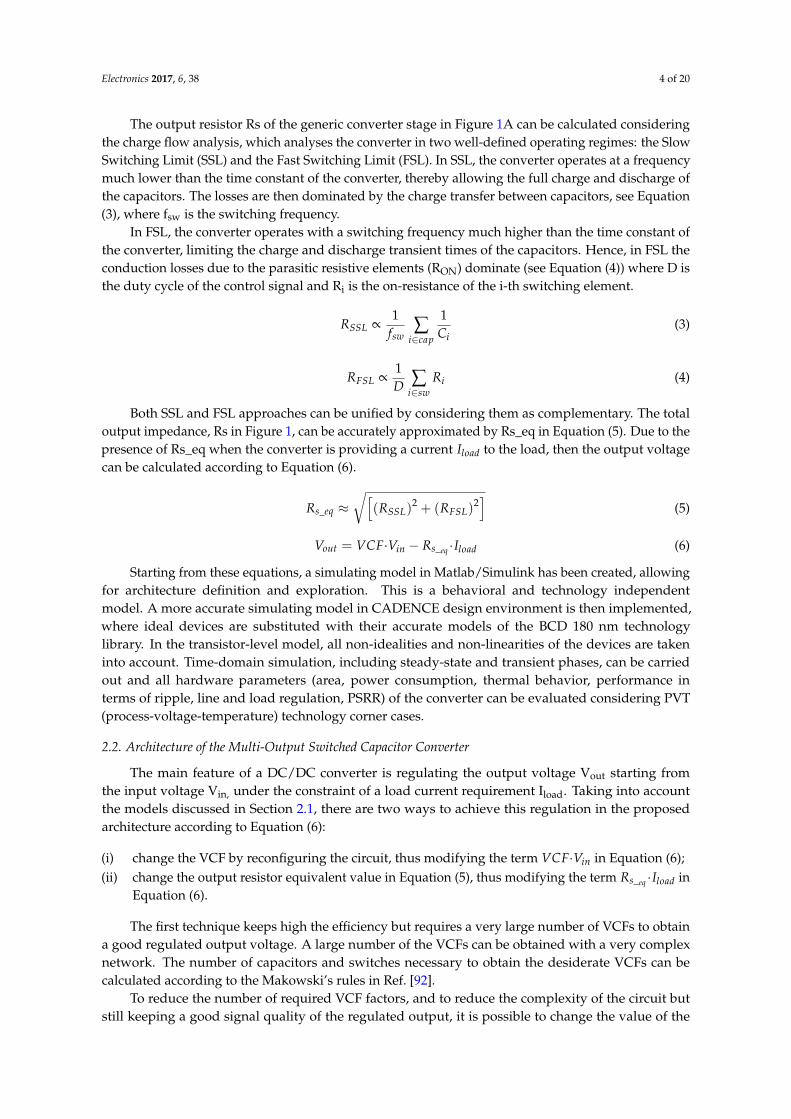
Moreover, each device (e.g., memory, sensor, microcontroller, RF transceiver) in a complex IoTsystem or CPS may require a different supply voltage level to optimize its performance. Therefore,the power management unit needs more than one output voltage. To this aim, we propose a modularand scalable architecture for the converter (see Figure 2) that can be expanded or reduced in relation tothe application.
Electronics 2017, 6, 38 5 of 20
and scalable architecture for the converter (see Figure 2) that can be expanded or reduced in relation
to the application.
Figure 2. Generic converter architecture based on multi switched capacitor (SC) and linear (LIN) converters.
The basic idea is to have a cascade of switched capacitor converter stages, SC‐1, SC‐2 and SC‐N
in Figure 2, each with a configurable VCF, being VCFi the VCF of the i‐th switching converter stage
SC‐i with i = 1, 2, …N. If a stage works in step‐up mode then VCF > 1, otherwise in step‐down mode
VCF < 1. This way, the overall VCF for the whole cascade of switching converters, i.e., Vx/Vin in
Figure 2, is the product of all the VCFi values of the N converter stages.
Once Vx in Figure 2 is regulated from Vin, thanks to the switched capacitors stages, then, at the
end of the cascade, several linear regulators are placed in parallel to obtain multiple‐output voltages.
In the example case of Figure 2, four linear regulators are placed in parallel to obtain four output
regulated voltages. The linear converters can only work as step‐down converters and their efficiency
levels depend on the difference between their input, Vx in Figure 2, and their output voltages, VoA
or VoB or VoC or VoD in the example of Figure 2.
If the input and output voltages of a linear converter are similar, they have an acceptable
efficiency level. Therefore, the purpose of the cascade of SC converters in Figure 2 is to reduce or
increase the input voltage Vin to put the linear converters at the last stage (LIN‐A, LIN‐B, LIN‐C, and
LIN‐D in Figure 2) in their best working conditions. In addition, the use of linear converters to obtain
different output voltages improves the quality of the output in terms of line regulation, load
regulation, ripple, and power supply rejection ratio (PSRR).
The switching converters with inductors have a high efficiency but only one output voltage. A
greater number of outputs requires more than one inductor, e.g., a converter for each output voltage
level. Alternatively, some linear converters in cascade can be used, but this leads to the loss of benefits
in terms of efficiency of the inductor‐based converter.
3. Designed DC/DC Converter
3.1. DC/DC Architecture and Circuit‐Level Design
The proposed power converter has been designed following the models and architecture
discussed in Section 2 and configured to face a very wide input voltage range (from 1 V to 60 V), thus
covering all possible requirements of an IoT or CPS node. Particularly, a four‐stage architecture has
been implemented, see Figure 3, where the first three stages are SC stages, each with a VCF that can
be selected as ×2, ×1, ×1/2 and ×1/3.
Figure 2. Generic converter architecture based on multi switched capacitor (SC) and linear(LIN) converters.
The basic idea is to have a cascade of switched capacitor converter stages, SC-1, SC-2 and SC-Nin Figure 2, each with a configurable VCF, being VCFi the VCF of the i-th switching converter stageSC-i with i = 1, 2, . . . N. If a stage works in step-up mode then VCF > 1, otherwise in step-down modeVCF < 1. This way, the overall VCF for the whole cascade of switching converters, i.e., Vx/Vin inFigure 2, is the product of all the VCFi values of the N converter stages.
Once Vx in Figure 2 is regulated from Vin, thanks to the switched capacitors stages, then, at theend of the cascade, several linear regulators are placed in parallel to obtain multiple-output voltages.In the example case of Figure 2, four linear regulators are placed in parallel to obtain four outputregulated voltages. The linear converters can only work as step-down converters and their efficiencylevels depend on the difference between their input, Vx in Figure 2, and their output voltages, VoA orVoB or VoC or VoD in the example of Figure 2.
If the input and output voltages of a linear converter are similar, they have an acceptable efficiencylevel. Therefore, the purpose of the cascade of SC converters in Figure 2 is to reduce or increase theinput voltage Vin to put the linear converters at the last stage (LIN-A, LIN-B, LIN-C, and LIN-D inFigure 2) in their best working conditions. In addition, the use of linear converters to obtain differentoutput voltages improves the quality of the output in terms of line regulation, load regulation, ripple,and power supply rejection ratio (PSRR).
The switching converters with inductors have a high efficiency but only one output voltage.A greater number of outputs requires more than one inductor, e.g., a converter for each output voltagelevel. Alternatively, some linear converters in cascade can be used, but this leads to the loss of benefitsin terms of efficiency of the inductor-based converter.
3. Designed DC/DC Converter
3.1. DC/DC Architecture and Circuit-Level Design
The proposed power converter has been designed following the models and architecture discussedin Section 2 and configured to face a very wide input voltage range (from 1 V to 60 V), thus coveringall possible requirements of an IoT or CPS node. Particularly, a four-stage architecture has been
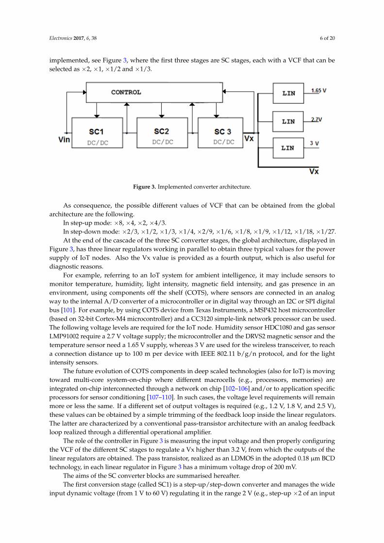
Electronics 2017, 6, 38 6 of 20
implemented, see Figure 3, where the first three stages are SC stages, each with a VCF that can beselected as ×2, ×1, ×1/2 and ×1/3.Electronics 2017, 6, 38 6 of 20
Figure 3. Implemented converter architecture.
As consequence, the possible different values of VCF that can be obtained from the global
architecture are the following.
In step‐up mode: ×8, ×4, ×2, ×4/3.
In step‐down mode: ×2/3, ×1/2, ×1/3, ×1/4, ×2/9, ×1/6, ×1/8, ×1/9, ×1/12, ×1/18, ×1/27.
At the end of the cascade of the three SC converter stages, the global architecture, displayed in
Figure 3, has three linear regulators working in parallel to obtain three typical values for the power
supply of IoT nodes. Also the Vx value is provided as a fourth output, which is also useful for
diagnostic reasons.
For example, referring to an IoT system for ambient intelligence, it may include sensors to
monitor temperature, humidity, light intensity, magnetic field intensity, and gas presence in an
environment, using components off the shelf (COTS), where sensors are connected in an analog way
to the internal A/D converter of a microcontroller or in digital way through an I2C or SPI digital bus
[101]. For example, by using COTS device from Texas Instruments, a MSP432 host microcontroller
(based on 32‐bit Cortex‐M4 microcontroller) and a CC3120 simple‐link network processor can be used.
The following voltage levels are required for the IoT node. Humidity sensor HDC1080 and gas sensor
LMP91002 require a 2.7 V voltage supply; the microcontroller and the DRVS2 magnetic sensor and
the temperature sensor need a 1.65 V supply, whereas 3 V are used for the wireless transceiver, to
reach a connection distance up to 100 m per device with IEEE 802.11 b/g/n protocol, and for the light
intensity sensors.
The future evolution of COTS components in deep scaled technologies (also for IoT) is moving
toward multi‐core system‐on‐chip where different macrocells (e.g., processors, memories) are
integrated on‐chip interconnected through a network on chip [102–106] and/or to application specific
processors for sensor conditioning [107–110]. In such cases, the voltage level requirements will
remain more or less the same. If a different set of output voltages is required (e.g., 1.2 V, 1.8 V, and
2.5 V), these values can be obtained by a simple trimming of the feedback loop inside the linear
regulators, The latter are characterized by a conventional pass‐transistor architecture with an analog
feedback loop realized through a differential operational amplifier.
The role of the controller in Figure 3 is measuring the input voltage and then properly
configuring the VCF of the different SC stages to regulate a Vx higher than 3.2 V, from which the
outputs of the linear regulators are obtained. The pass transistor, realized as an LDMOS in the
adopted 0.18 μm BCD technology, in each linear regulator in Figure 3 has a minimum voltage drop
of 200 mV.
The aims of the SC converter blocks are summarised hereafter.
The first conversion stage (called SC1) is a step‐up/step‐down converter and manages the wide
input dynamic voltage (from 1 V to 60 V) regulating it in the range 2 V (e.g., step‐up ×2 of an input
voltage of 1 V) to 20 V (e.g., step‐down ×1/3 of an input voltage of 60V). This is the most challenging
stage since it faces the highest voltage levels.
Figure 3. Implemented converter architecture.
As consequence, the possible different values of VCF that can be obtained from the globalarchitecture are the following.
In step-up mode: ×8, ×4, ×2, ×4/3.In step-down mode: ×2/3, ×1/2, ×1/3, ×1/4, ×2/9, ×1/6, ×1/8, ×1/9, ×1/12, ×1/18, ×1/27.At the end of the cascade of the three SC converter stages, the global architecture, displayed in
Figure 3, has three linear regulators working in parallel to obtain three typical values for the powersupply of IoT nodes. Also the Vx value is provided as a fourth output, which is also useful fordiagnostic reasons.
For example, referring to an IoT system for ambient intelligence, it may include sensors tomonitor temperature, humidity, light intensity, magnetic field intensity, and gas presence in anenvironment, using components off the shelf (COTS), where sensors are connected in an analogway to the internal A/D converter of a microcontroller or in digital way through an I2C or SPI digitalbus [101]. For example, by using COTS device from Texas Instruments, a MSP432 host microcontroller(based on 32-bit Cortex-M4 microcontroller) and a CC3120 simple-link network processor can be used.The following voltage levels are required for the IoT node. Humidity sensor HDC1080 and gas sensorLMP91002 require a 2.7 V voltage supply; the microcontroller and the DRVS2 magnetic sensor and thetemperature sensor need a 1.65 V supply, whereas 3 V are used for the wireless transceiver, to reacha connection distance up to 100 m per device with IEEE 802.11 b/g/n protocol, and for the lightintensity sensors.
The future evolution of COTS components in deep scaled technologies (also for IoT) is movingtoward multi-core system-on-chip where different macrocells (e.g., processors, memories) areintegrated on-chip interconnected through a network on chip [102–106] and/or to application specificprocessors for sensor conditioning [107–110]. In such cases, the voltage level requirements will remainmore or less the same. If a different set of output voltages is required (e.g., 1.2 V, 1.8 V, and 2.5 V),these values can be obtained by a simple trimming of the feedback loop inside the linear regulators.The latter are characterized by a conventional pass-transistor architecture with an analog feedbackloop realized through a differential operational amplifier.
The role of the controller in Figure 3 is measuring the input voltage and then properly configuringthe VCF of the different SC stages to regulate a Vx higher than 3.2 V, from which the outputs of thelinear regulators are obtained. The pass transistor, realized as an LDMOS in the adopted 0.18 µm BCDtechnology, in each linear regulator in Figure 3 has a minimum voltage drop of 200 mV.
The aims of the SC converter blocks are summarised hereafter.The first conversion stage (called SC1) is a step-up/step-down converter and manages the wide
input dynamic voltage (from 1 V to 60 V) regulating it in the range 2 V (e.g., step-up ×2 of an input

Electronics 2017, 6, 38 7 of 20
voltage of 1 V) to 20 V (e.g., step-down ×1/3 of an input voltage of 60V). This is the most challengingstage since it faces the highest voltage levels.
The second and the third conversion stages (called SC2 and SC3 in Figure 3) reduce the outputresistance of the whole converter to ensure the correct operation of the final cascaded linear convertersso that Vx is about 4 V when there is 1 V at the input of the converter. Instead, 60 V at Vin is regulatedwith a step-down factor ×1/18 to a voltage of 3.33 V. To be noted that, by using for 60 V a step-downfactor ×1/12, then Vx is 5 V, which is another typical value for voltage supply of COTS components inIoT and CPS nodes.
To ensure the correct functionality of the 3 V linear converter, the VCFs thresholds are set to obtainan output voltage of the SC sub-system higher than 3.2 V for all the input dynamic. The system isoptimized to supply a variable number of loads. It has been sized to face current requirements of300 mA for the 3 V output and 2.7 V output and 120 mA for the 1.65 V.
According to the Ref. [92] to obtain the desiderate VCFs the SC architecture displayed in Figure 4is used. The proposed circuit in Figure 4 uses two fly capacitors and a buffer capacitor.
Electronics 2017, 6, 38 7 of 20
The second and the third conversion stages (called SC2 and SC3 in Figure 3) reduce the output
resistance of the whole converter to ensure the correct operation of the final cascaded linear
converters so that Vx is about 4 V when there is 1 V at the input of the converter. Instead, 60 V at Vin
is regulated with a step‐down factor ×1/18 to a voltage of 3.33 V. To be noted that, by using for 60 V
a step‐down factor ×1/12, then Vx is 5 V, which is another typical value for voltage supply of COTS
components in IoT and CPS nodes.
To ensure the correct functionality of the 3 V linear converter, the VCFs thresholds are set to
obtain an output voltage of the SC sub‐system higher than 3.2 V for all the input dynamic. The system
is optimized to supply a variable number of loads. It has been sized to face current requirements of
300 mA for the 3 V output and 2.7 V output and 120 mA for the 1.65 V.
According to the Ref. [92] to obtain the desiderate VCFs the SC architecture displayed in Figure
4 is used. The proposed circuit in Figure 4 uses two fly capacitors and a buffer capacitor.
Figure 4. Circuit level design of the SC stages SC‐1, SC‐2, and SC‐3 in Figure 3.
For this application, a 0.18 μm BCD technology is chosen to manage voltage levels up to 60 V.
The specific technology has an influence on the ON‐resistance of the switches and hence on the RFSL
value. Each switch in Figure 4 is sized according to the voltage to be faced and its role in the converter.
Each switch can be made with single P‐MOS/N‐MOS or with a complex configuration up to four
MOS devices.
Indeed, in the architecture of Figure 3, depending on the stage where the switch is used, the
device that implements the switch may face voltage levels going from few Volts to several tens of
Volts. Hence, three different circuit configurations, listed hereafter, can be used, which require from
one to four transistors.
(1) When facing low voltages the switch may be realized with a simple MOS transistor.
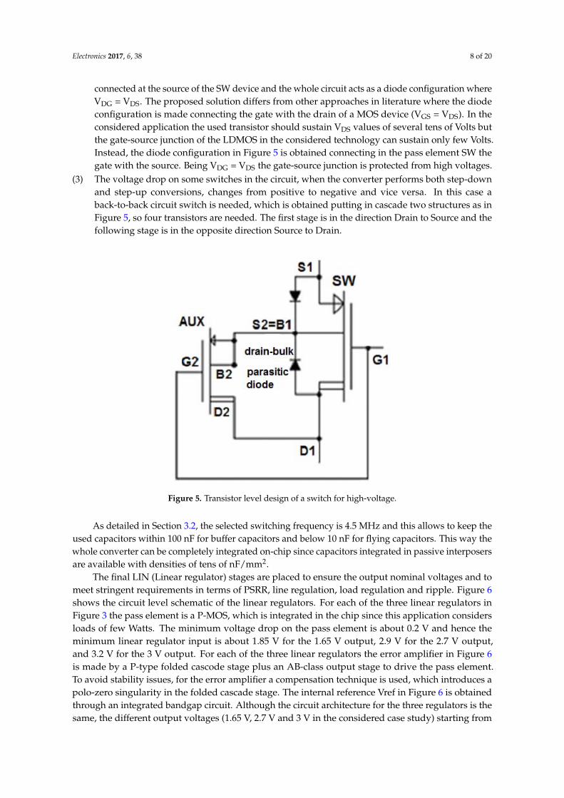
(2) When facing higher voltages, an LDMOS (Laterally Diffused Metal Oxide Semiconductor),
available in the BCD technology, is used as switch. In the selected configuration (see in Figure 5
the case of a P‐MOS switch) two MOS devices are used: one is the switching element (device SW
in Figure 5), and the other is another device (AUX in Figure 5) that connects the bulk of the pass
transistor SW to his drain to bypass the drain‐bulk parasitic diode. Indeed, in Figure 5 if the bulk
is connected at the source of the device SW, then during some transients the bulk can have a
lower potential than the drain. In this case, the current can flow inside the drain‐bulk parasitic
diode and is not possible to turn OFF the MOS just driving the gate voltage. Furthermore, the
parasitic BJT in each LDMOS may inject current in the substrate. This current injection, if not
avoided, could have destructive effects. To avoid these issues the circuit with two MOS in Figure
5 may be used. In this circuit the gate driver is connected between the gate and the source of the
SW pass transistor to handle its VGS. This way, when the gate driving signal is 0 V the gate is
connected at the source of the SW device and the whole circuit acts as a diode configuration
where VDG = VDS. The proposed solution differs from other approaches in literature where the
diode configuration is made connecting the gate with the drain of a MOS device (VGS = VDS). In
the considered application the used transistor should sustain VDS values of several tens of Volts
but the gate‐source junction of the LDMOS in the considered technology can sustain only few
Figure 4. Circuit level design of the SC stages SC-1, SC-2, and SC-3 in Figure 3.
For this application, a 0.18 µm BCD technology is chosen to manage voltage levels up to 60 V.The specific technology has an influence on the ON-resistance of the switches and hence on the RFSL
value. Each switch in Figure 4 is sized according to the voltage to be faced and its role in the converter.Each switch can be made with single P-MOS/N-MOS or with a complex configuration up to fourMOS devices.
Indeed, in the architecture of Figure 3, depending on the stage where the switch is used, the devicethat implements the switch may face voltage levels going from few Volts to several tens of Volts.Hence, three different circuit configurations, listed hereafter, can be used, which require from one tofour transistors.
(1) When facing low voltages the switch may be realized with a simple MOS transistor.(2) When facing higher voltages, an LDMOS (Laterally Diffused Metal Oxide Semiconductor),
available in the BCD technology, is used as switch. In the selected configuration (see in Figure 5the case of a P-MOS switch) two MOS devices are used: one is the switching element (device SWin Figure 5), and the other is another device (AUX in Figure 5) that connects the bulk of the passtransistor SW to his drain to bypass the drain-bulk parasitic diode. Indeed, in Figure 5 if the bulkis connected at the source of the device SW, then during some transients the bulk can have a lowerpotential than the drain. In this case, the current can flow inside the drain-bulk parasitic diodeand is not possible to turn OFF the MOS just driving the gate voltage. Furthermore, the parasiticBJT in each LDMOS may inject current in the substrate. This current injection, if not avoided,could have destructive effects. To avoid these issues the circuit with two MOS in Figure 5 maybe used. In this circuit the gate driver is connected between the gate and the source of theSW pass transistor to handle its VGS. This way, when the gate driving signal is 0 V the gate is
Electronics 2017, 6, 38 8 of 20
connected at the source of the SW device and the whole circuit acts as a diode configuration whereVDG = VDS. The proposed solution differs from other approaches in literature where the diodeconfiguration is made connecting the gate with the drain of a MOS device (VGS = VDS). In theconsidered application the used transistor should sustain VDS values of several tens of Volts butthe gate-source junction of the LDMOS in the considered technology can sustain only few Volts.Instead, the diode configuration in Figure 5 is obtained connecting in the pass element SW thegate with the source. Being VDG = VDS the gate-source junction is protected from high voltages.
(3) The voltage drop on some switches in the circuit, when the converter performs both step-downand step-up conversions, changes from positive to negative and vice versa. In this case aback-to-back circuit switch is needed, which is obtained putting in cascade two structures as inFigure 5, so four transistors are needed. The first stage is in the direction Drain to Source and thefollowing stage is in the opposite direction Source to Drain.
Electronics 2017, 6, 38 8 of 20
Volts. Instead, the diode configuration in Figure 5 is obtained connecting in the pass element SW
the gate with the source. Being VDG = VDS the gate‐source junction is protected from high voltages.
(3) The voltage drop on some switches in the circuit, when the converter performs both step‐down
and step‐up conversions, changes from positive to negative and vice versa. In this case a back‐
to‐back circuit switch is needed, which is obtained putting in cascade two structures as in Figure
5, so four transistors are needed. The first stage is in the direction Drain to Source and the
following stage is in the opposite direction Source to Drain.
Figure 5. Transistor level design of a switch for high‐voltage.
As detailed in Section 3.2, the selected switching frequency is 4.5 MHz and this allows to keep
the used capacitors within 100 nF for buffer capacitors and below 10 nF for flying capacitors. This
way the whole converter can be completely integrated on‐chip since capacitors integrated in passive
interposers are available with densities of tens of nF/mm2.
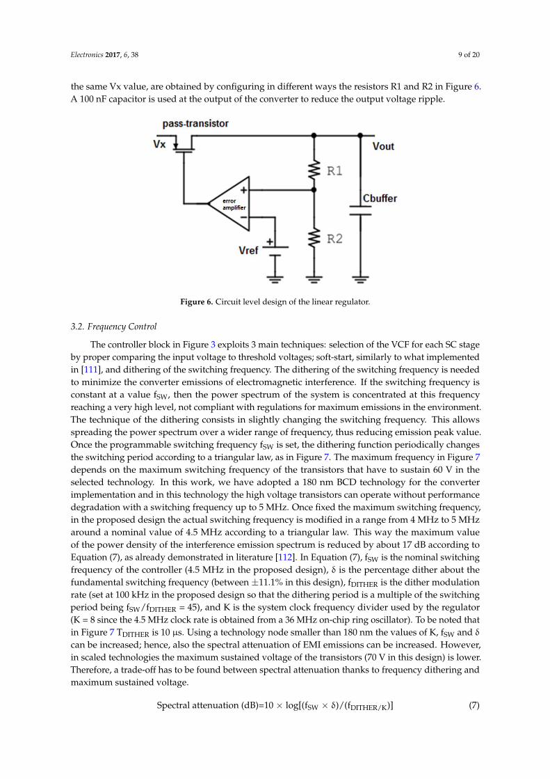
The final LIN (Linear regulator) stages are placed to ensure the output nominal voltages and to
meet stringent requirements in terms of PSRR, line regulation, load regulation and ripple. Figure 6
shows the circuit level schematic of the linear regulators. For each of the three linear regulators in
Figure 3 the pass element is a P‐MOS, which is integrated in the chip since this application considers
loads of few Watts. The minimum voltage drop on the pass element is about 0.2 V and hence the
minimum linear regulator input is about 1.85 V for the 1.65 V output, 2.9 V for the 2.7 V output, and
3.2 V for the 3V output. For each of the three linear regulators the error amplifier in Figure 6 is made
by a P‐type folded cascode stage plus an AB‐class output stage to drive the pass element. To avoid
stability issues, for the error amplifier a compensation technique is used, which introduces a polo‐
zero singularity in the folded cascade stage. The internal reference Vref in Figure 6 is obtained
through an integrated bandgap circuit. Although the circuit architecture for the three regulators is
the same, the different output voltages (1.65 V, 2.7 V and 3 V in the considered case study) starting
from the same Vx value, are obtained by configuring in different ways the resistors R1 and R2 in
Figure 6. A 100 nF capacitor is used at the output of the converter to reduce the output voltage ripple.
Figure 5. Transistor level design of a switch for high-voltage.
As detailed in Section 3.2, the selected switching frequency is 4.5 MHz and this allows to keep theused capacitors within 100 nF for buffer capacitors and below 10 nF for flying capacitors. This way thewhole converter can be completely integrated on-chip since capacitors integrated in passive interposersare available with densities of tens of nF/mm2.
The final LIN (Linear regulator) stages are placed to ensure the output nominal voltages and tomeet stringent requirements in terms of PSRR, line regulation, load regulation and ripple. Figure 6shows the circuit level schematic of the linear regulators. For each of the three linear regulators inFigure 3 the pass element is a P-MOS, which is integrated in the chip since this application considersloads of few Watts. The minimum voltage drop on the pass element is about 0.2 V and hence theminimum linear regulator input is about 1.85 V for the 1.65 V output, 2.9 V for the 2.7 V output,and 3.2 V for the 3 V output. For each of the three linear regulators the error amplifier in Figure 6is made by a P-type folded cascode stage plus an AB-class output stage to drive the pass element.To avoid stability issues, for the error amplifier a compensation technique is used, which introduces apolo-zero singularity in the folded cascade stage. The internal reference Vref in Figure 6 is obtainedthrough an integrated bandgap circuit. Although the circuit architecture for the three regulators is thesame, the different output voltages (1.65 V, 2.7 V and 3 V in the considered case study) starting from
Electronics 2017, 6, 38 9 of 20
the same Vx value, are obtained by configuring in different ways the resistors R1 and R2 in Figure 6.A 100 nF capacitor is used at the output of the converter to reduce the output voltage ripple.Electronics 2017, 6, 38 9 of 20
Figure 6. Circuit level design of the linear regulator.
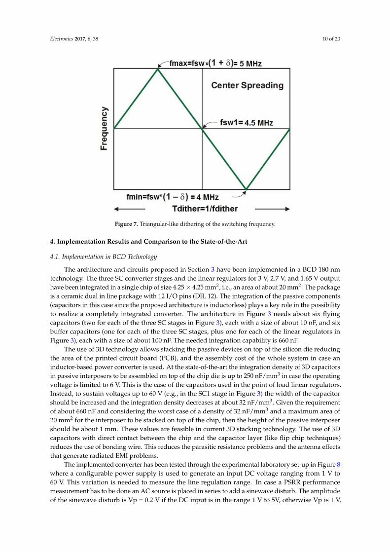
3.2. Frequency Control
The controller block in Figure 3 exploits 3 main techniques: selection of the VCF for each SC
stage by proper comparing the input voltage to threshold voltages; soft‐start, similarly to what
implemented in [111], and dithering of the switching frequency. The dithering of the switching
frequency is needed to minimize the converter emissions of electromagnetic interference. If the
switching frequency is constant at a value fSW, then the power spectrum of the system is concentrated
at this frequency reaching a very high level, not compliant with regulations for maximum emissions
in the environment. The technique of the dithering consists in slightly changing the switching
frequency. This allows spreading the power spectrum over a wider range of frequency, thus reducing
emission peak value. Once the programmable switching frequency fSW is set, the dithering function
periodically changes the switching period according to a triangular law, as in Figure 7. The maximum
frequency in Figure 7 depends on the maximum switching frequency of the transistors that have to
sustain 60 V in the selected technology. In this work, we have adopted a 180 nm BCD technology for
the converter implementation and in this technology the high voltage transistors can operate without
performance degradation with a switching frequency up to 5 MHz. Once fixed the maximum
switching frequency, in the proposed design the actual switching frequency is modified in a range
from 4 MHz to 5 MHz around a nominal value of 4.5 MHz according to a triangular law. This way
the maximum value of the power density of the interference emission spectrum is reduced by about
17 dB according to Equation (7), as already demonstrated in literature [112]. In Equation (7), fSW is the
nominal switching frequency of the controller (4.5 MHz in the proposed design), δ is the percentage
dither about the fundamental switching frequency (between ±11.1% in this design), fDITHER is the
dither modulation rate (set at 100 kHz in the proposed design so that the dithering period is a
multiple of the switching period being fSW/fDITHER = 45), and K is the system clock frequency divider
used by the regulator (K = 8 since the 4.5 MHz clock rate is obtained from a 36 MHz on‐chip ring
oscillator). To be noted that in Figure 7 TDITHER is 10 μs. Using a technology node smaller than 180 nm
the values of K, fSW and δ can be increased; hence, also the spectral attenuation of EMI emissions can
be increased. However, in scaled technologies the maximum sustained voltage of the transistors (70
V in this design) is lower. Therefore, a trade‐off has to be found between spectral attenuation thanks
to frequency dithering and maximum sustained voltage.
Spectral attenuation (dB)=10 × log[(fSW × δ) / (fDITHER/K)] (7)
Figure 6. Circuit level design of the linear regulator.
3.2. Frequency Control
The controller block in Figure 3 exploits 3 main techniques: selection of the VCF for each SC stageby proper comparing the input voltage to threshold voltages; soft-start, similarly to what implementedin [111], and dithering of the switching frequency. The dithering of the switching frequency is neededto minimize the converter emissions of electromagnetic interference. If the switching frequency isconstant at a value fSW, then the power spectrum of the system is concentrated at this frequencyreaching a very high level, not compliant with regulations for maximum emissions in the environment.The technique of the dithering consists in slightly changing the switching frequency. This allowsspreading the power spectrum over a wider range of frequency, thus reducing emission peak value.Once the programmable switching frequency fSW is set, the dithering function periodically changesthe switching period according to a triangular law, as in Figure 7. The maximum frequency in Figure 7depends on the maximum switching frequency of the transistors that have to sustain 60 V in theselected technology. In this work, we have adopted a 180 nm BCD technology for the converterimplementation and in this technology the high voltage transistors can operate without performancedegradation with a switching frequency up to 5 MHz. Once fixed the maximum switching frequency,in the proposed design the actual switching frequency is modified in a range from 4 MHz to 5 MHzaround a nominal value of 4.5 MHz according to a triangular law. This way the maximum valueof the power density of the interference emission spectrum is reduced by about 17 dB according toEquation (7), as already demonstrated in literature [112]. In Equation (7), fSW is the nominal switchingfrequency of the controller (4.5 MHz in the proposed design), δ is the percentage dither about thefundamental switching frequency (between ±11.1% in this design), fDITHER is the dither modulationrate (set at 100 kHz in the proposed design so that the dithering period is a multiple of the switchingperiod being fSW/fDITHER = 45), and K is the system clock frequency divider used by the regulator(K = 8 since the 4.5 MHz clock rate is obtained from a 36 MHz on-chip ring oscillator). To be noted thatin Figure 7 TDITHER is 10 µs. Using a technology node smaller than 180 nm the values of K, fSW and δ
can be increased; hence, also the spectral attenuation of EMI emissions can be increased. However,in scaled technologies the maximum sustained voltage of the transistors (70 V in this design) is lower.Therefore, a trade-off has to be found between spectral attenuation thanks to frequency dithering andmaximum sustained voltage.
Spectral attenuation (dB)=10 × log[(fSW × δ)/(fDITHER/K)] (7)
Electronics 2017, 6, 38 10 of 20Electronics 2017, 6, 38 10 of 20
Figure 7. Triangular‐like dithering of the switching frequency.
4. Implementation Results and Comparison to the State‐of‐the‐Art
4.1. Implementation in BCD Technology
The architecture and circuits proposed in Section 3 have been implemented in a BCD 180 nm
technology. The three SC converter stages and the linear regulators for 3 V, 2.7 V, and 1.65 V output
have been integrated in a single chip of size 4.25 × 4.25 mm2, i.e., an area of about 20 mm2. The package
is a ceramic dual in line package with 12 I/O pins (DIL 12). The integration of the passive components
(capacitors in this case since the proposed architecture is inductorless) plays a key role in the
possibility to realize a completely integrated converter. The architecture in Figure 3 needs about six
flying capacitors (two for each of the three SC stages in Figure 3), each with a size of about 10 nF, and
six buffer capacitors (one for each of the three SC stages, plus one for each of the linear regulators in
Figure 3), each with a size of about 100 nF. The needed integration capability is 660 nF.
The use of 3D technology allows stacking the passive devices on top of the silicon die reducing
the area of the printed circuit board (PCB), and the assembly cost of the whole system in case an
inductor‐based power converter is used. At the state‐of‐the‐art the integration density of 3D
capacitors in passive interposers to be assembled on top of the chip die is up to 250 nF/mm3 in case
the operating voltage is limited to 6 V. This is the case of the capacitors used in the point of load linear
regulators. Instead, to sustain voltages up to 60 V (e.g., in the SC1 stage in Figure 3) the width of the
capacitor should be increased and the integration density decreases at about 32 nF/mm3. Given the
requirement of about 660 nF and considering the worst case of a density of 32 nF/mm3 and a
maximum area of 20 mm2 for the interposer to be stacked on top of the chip, then the height of the
passive interposer should be about 1 mm. These values are feasible in current 3D stacking technology.
The use of 3D capacitors with direct contact between the chip and the capacitor layer (like flip chip
techniques) reduces the use of bonding wire. This reduces the parasitic resistance problems and the
antenna effects that generate radiated EMI problems.
The implemented converter has been tested through the experimental laboratory set‐up in
Figure 8 where a configurable power supply is used to generate an input DC voltage ranging from 1
V to 60 V. This variation is needed to measure the line regulation range. In case a PSRR performance
measurement has to be done an AC source is placed in series to add a sinewave disturb. The
amplitude of the sinewave disturb is Vp = 0.2 V if the DC input is in the range 1 V to 5V, otherwise
Vp is 1 V. If the test does not include the PSRR evaluation, the AC source is bypassed. The three
voltage outputs plus the Vx output (see Figure 3) are measured through a multimeter. At the output
Figure 7. Triangular-like dithering of the switching frequency.
4. Implementation Results and Comparison to the State-of-the-Art
4.1. Implementation in BCD Technology
The architecture and circuits proposed in Section 3 have been implemented in a BCD 180 nmtechnology. The three SC converter stages and the linear regulators for 3 V, 2.7 V, and 1.65 V outputhave been integrated in a single chip of size 4.25× 4.25 mm2, i.e., an area of about 20 mm2. The packageis a ceramic dual in line package with 12 I/O pins (DIL 12). The integration of the passive components(capacitors in this case since the proposed architecture is inductorless) plays a key role in the possibilityto realize a completely integrated converter. The architecture in Figure 3 needs about six flyingcapacitors (two for each of the three SC stages in Figure 3), each with a size of about 10 nF, and sixbuffer capacitors (one for each of the three SC stages, plus one for each of the linear regulators inFigure 3), each with a size of about 100 nF. The needed integration capability is 660 nF.
The use of 3D technology allows stacking the passive devices on top of the silicon die reducingthe area of the printed circuit board (PCB), and the assembly cost of the whole system in case aninductor-based power converter is used. At the state-of-the-art the integration density of 3D capacitorsin passive interposers to be assembled on top of the chip die is up to 250 nF/mm3 in case the operatingvoltage is limited to 6 V. This is the case of the capacitors used in the point of load linear regulators.Instead, to sustain voltages up to 60 V (e.g., in the SC1 stage in Figure 3) the width of the capacitorshould be increased and the integration density decreases at about 32 nF/mm3. Given the requirementof about 660 nF and considering the worst case of a density of 32 nF/mm3 and a maximum area of20 mm2 for the interposer to be stacked on top of the chip, then the height of the passive interposershould be about 1 mm. These values are feasible in current 3D stacking technology. The use of 3Dcapacitors with direct contact between the chip and the capacitor layer (like flip chip techniques)reduces the use of bonding wire. This reduces the parasitic resistance problems and the antenna effectsthat generate radiated EMI problems.
The implemented converter has been tested through the experimental laboratory set-up in Figure 8where a configurable power supply is used to generate an input DC voltage ranging from 1 V to60 V. This variation is needed to measure the line regulation range. In case a PSRR performancemeasurement has to be done an AC source is placed in series to add a sinewave disturb. The amplitudeof the sinewave disturb is Vp = 0.2 V if the DC input is in the range 1 V to 5V, otherwise Vp is 1 V.

Electronics 2017, 6, 38 11 of 20
If the test does not include the PSRR evaluation, the AC source is bypassed. The three voltage outputsplus the Vx output (see Figure 3) are measured through a multimeter. At the output of the threelinear regulators, three configurable loads are applied so that we can measure also the load regulationperformance, i.e., we can make several tests with different load currents.
Electronics 2017, 6, 38 11 of 20
of the three linear regulators, three configurable loads are applied so that we can measure also the
load regulation performance, i.e., we can make several tests with different load currents.
Figure 8. Schematic of the experimental test set‐up and chip prototype.
Figure 9 shows the achieved power efficiency as a function of the input regulation voltage
ranging from 1 V to 60 V when the output is regulated at 3 V. For comparison also the performance
achieved by an ideal linear regulator and by a commercially‐available converter, the Analog Devices
chip LT3245 in [96], are shown. It is worth noting that the proposed converter is the only one able to
regulate a 3 V output starting from a voltage in the range 1 V to 60 V, and hence acting bot as step‐
up or step‐down converter. Instead, the linear regulator can work only as step‐down. The LT3245
DC/DC converter has a working range of about 33 V, from 3 V to 38 V. Hence, it cannot be used with
energy harvesting systems where the harvested power source is usually working with voltage levels
below 3 V. From an efficiency point of view, the proposed converter outperforms the LT3245 for all
input voltages above 15 V. The proposed design has an efficiency ranging from about 50% to 70%
when the input voltage varies from 1 V to 60 V. The linear regulator is efficient only for very low
inputs. Its efficiency is reduced down to 5% when the input voltage increases to 60 V. Repeating the
power efficiency analysis also for the other outputs (2.7 V and 1.65 V in the considered design), similar
results are obtained.
Figure 9. Power efficiency of the 3V output stage when Vin varies from 1 V to 60 V.
Figure 10 shows the load regulation capability of the proposed converter. The output voltage for
each of the three outputs is evaluated for different values of the load current in the range from 0 to
300 mA for the 3 V and the 2.7 V outputs and in the range 0 to 120 mA for the 1.65 V output. In Figure
10, the input voltage is kept at a constant value of 12 V. Instead, Figure 11 shows the line regulation
capability of the proposed converter, i.e., how the output voltage varies (for three outputs) when the
input voltage changes from 1 V to 60 V. The output current is considered for two different load values:
10 mA and 300 mA for the 3 V and 2.7 V outputs, and 10 mA and 120 mA for the 1.65 V output.
0
10
20
30
40
50
60
70
80
90
0 5 10 15 20 25 30 35 40 45 50 55 60Vou
t =
3V
, pow
er e
ffic
ien
cy %
Vin, V
Ideal Linear Converter
LT3245
This work
Figure 8. Schematic of the experimental test set-up and chip prototype.
Figure 9 shows the achieved power efficiency as a function of the input regulation voltage rangingfrom 1 V to 60 V when the output is regulated at 3 V. For comparison also the performance achieved byan ideal linear regulator and by a commercially-available converter, the Analog Devices chip LT3245in [96], are shown. It is worth noting that the proposed converter is the only one able to regulate a 3 Voutput starting from a voltage in the range 1 V to 60 V, and hence acting bot as step-up or step-downconverter. Instead, the linear regulator can work only as step-down. The LT3245 DC/DC converterhas a working range of about 33 V, from 3 V to 38 V. Hence, it cannot be used with energy harvestingsystems where the harvested power source is usually working with voltage levels below 3 V. From anefficiency point of view, the proposed converter outperforms the LT3245 for all input voltages above15 V. The proposed design has an efficiency ranging from about 50% to 70% when the input voltagevaries from 1 V to 60 V. The linear regulator is efficient only for very low inputs. Its efficiency isreduced down to 5% when the input voltage increases to 60 V. Repeating the power efficiency analysisalso for the other outputs (2.7 V and 1.65 V in the considered design), similar results are obtained.
Electronics 2017, 6, 38 11 of 20
of the three linear regulators, three configurable loads are applied so that we can measure also the
load regulation performance, i.e., we can make several tests with different load currents.
Figure 8. Schematic of the experimental test set‐up and chip prototype.
Figure 9 shows the achieved power efficiency as a function of the input regulation voltage
ranging from 1 V to 60 V when the output is regulated at 3 V. For comparison also the performance
achieved by an ideal linear regulator and by a commercially‐available converter, the Analog Devices
chip LT3245 in [96], are shown. It is worth noting that the proposed converter is the only one able to
regulate a 3 V output starting from a voltage in the range 1 V to 60 V, and hence acting bot as step‐
up or step‐down converter. Instead, the linear regulator can work only as step‐down. The LT3245
DC/DC converter has a working range of about 33 V, from 3 V to 38 V. Hence, it cannot be used with
energy harvesting systems where the harvested power source is usually working with voltage levels
below 3 V. From an efficiency point of view, the proposed converter outperforms the LT3245 for all
input voltages above 15 V. The proposed design has an efficiency ranging from about 50% to 70%
when the input voltage varies from 1 V to 60 V. The linear regulator is efficient only for very low
inputs. Its efficiency is reduced down to 5% when the input voltage increases to 60 V. Repeating the
power efficiency analysis also for the other outputs (2.7 V and 1.65 V in the considered design), similar
results are obtained.
Figure 9. Power efficiency of the 3V output stage when Vin varies from 1 V to 60 V.
Figure 10 shows the load regulation capability of the proposed converter. The output voltage for
each of the three outputs is evaluated for different values of the load current in the range from 0 to
300 mA for the 3 V and the 2.7 V outputs and in the range 0 to 120 mA for the 1.65 V output. In Figure
10, the input voltage is kept at a constant value of 12 V. Instead, Figure 11 shows the line regulation
capability of the proposed converter, i.e., how the output voltage varies (for three outputs) when the
input voltage changes from 1 V to 60 V. The output current is considered for two different load values:
10 mA and 300 mA for the 3 V and 2.7 V outputs, and 10 mA and 120 mA for the 1.65 V output.
0
10
20
30
40
50
60
70
80
90
0 5 10 15 20 25 30 35 40 45 50 55 60Vou
t =
3V
, pow
er e
ffic
ien
cy %
Vin, V
Ideal Linear Converter
LT3245
This work
Figure 9. Power efficiency of the 3V output stage when Vin varies from 1 V to 60 V.
Figure 10 shows the load regulation capability of the proposed converter. The output voltagefor each of the three outputs is evaluated for different values of the load current in the range from0 to 300 mA for the 3 V and the 2.7 V outputs and in the range 0 to 120 mA for the 1.65 V output.In Figure 10, the input voltage is kept at a constant value of 12 V. Instead, Figure 11 shows the lineregulation capability of the proposed converter, i.e., how the output voltage varies (for three outputs)
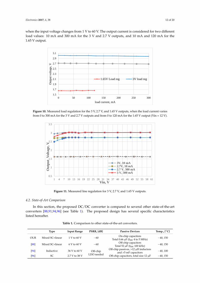
Electronics 2017, 6, 38 12 of 20
when the input voltage changes from 1 V to 60 V. The output current is considered for two differentload values: 10 mA and 300 mA for the 3 V and 2.7 V outputs, and 10 mA and 120 mA for the1.65 V output.
Electronics 2017, 6, 38 12 of 20
Figure 10. Measured load regulation for the 3 V, 2.7 V, and 1.65 V outputs, when the load current varies
from 0 to 300 mA for the 3 V and 2.7 V outputs and from 0 to 120 mA for the 1.65 V output (Vin = 12 V).
Figure 11. Measured line regulation for 3 V, 2.7 V, and 1.65 V outputs.
4.2. State‐of‐Art Comparison
In this section, the proposed DC/DC converter is compared to several other state‐of‐the‐art
converters [88,91,94,96] (see Table 1). The proposed design has several specific characteristics listed
hereafter.
Table 1. Comparison to other state‐of‐the‐art converters.
Type Input Range PSRR, [dB] Passive Devices Temp., [°C]
OUR Mixed SC+linear 1 V to 60 V −60 On‐chip capacitors
Total 0.66 μF (fSW 4 to 5 MHz) −40, 150
[88] Mixed SC+linear 6 V to 60 V −60 Off‐chip capacitors
Total 52 μF (fSW 100 kHz) −40, 150
[94] Inductive 36 V to 60 V Off‐chip
LDO needed
Off‐chip passives, >12 μH inductors
and >5 mF capacitors −40, 100
[96] SC 2.7 V to 38 V Off‐chip capacitors, total size 12 μF −40, 150
(1) The converter in this work is one of the few that avoid the use of cumbersome inductors, but at
the same time is facing voltages up to 60 V. Instead, inductors are up tens of μH in state‐of‐the‐
art converters with the same input voltage range [94].
1.5
1.7
1.9
2.1
2.3
2.5
2.7
2.9
3.1
0 50 100 150 200 250 300
Out
put v
olta
ge, V
load current, mA
1.65V Load reg 3V load reg
0.5
1
1.5
2
2.5
3
3.5
1 4 7 10 13 16 19 22 25 28 31 34 37 40 43 46 49 52 55 58 61
Ou
tpu
t V
olta
ge, V
Vin, V
3V, 10 mA2.7V, 10 mA2.7 V, 300 mA3 V, 300 mA
Figure 10. Measured load regulation for the 3 V, 2.7 V, and 1.65 V outputs, when the load current variesfrom 0 to 300 mA for the 3 V and 2.7 V outputs and from 0 to 120 mA for the 1.65 V output (Vin = 12 V).
Electronics 2017, 6, 38 12 of 20
Figure 10. Measured load regulation for the 3 V, 2.7 V, and 1.65 V outputs, when the load current varies
from 0 to 300 mA for the 3 V and 2.7 V outputs and from 0 to 120 mA for the 1.65 V output (Vin = 12 V).
Figure 11. Measured line regulation for 3 V, 2.7 V, and 1.65 V outputs.
4.2. State‐of‐Art Comparison
In this section, the proposed DC/DC converter is compared to several other state‐of‐the‐art
converters [88,91,94,96] (see Table 1). The proposed design has several specific characteristics listed
hereafter.
Table 1. Comparison to other state‐of‐the‐art converters.
Type Input Range PSRR, [dB] Passive Devices Temp., [°C]
OUR Mixed SC+linear 1 V to 60 V −60 On‐chip capacitors
Total 0.66 μF (fSW 4 to 5 MHz) −40, 150
[88] Mixed SC+linear 6 V to 60 V −60 Off‐chip capacitors
Total 52 μF (fSW 100 kHz) −40, 150
[94] Inductive 36 V to 60 V Off‐chip
LDO needed
Off‐chip passives, >12 μH inductors
and >5 mF capacitors −40, 100
[96] SC 2.7 V to 38 V Off‐chip capacitors, total size 12 μF −40, 150
(1) The converter in this work is one of the few that avoid the use of cumbersome inductors, but at
the same time is facing voltages up to 60 V. Instead, inductors are up tens of μH in state‐of‐the‐
art converters with the same input voltage range [94].
1.5
1.7
1.9
2.1
2.3
2.5
2.7
2.9
3.1
0 50 100 150 200 250 300
Out
put v
olta
ge, V
load current, mA
1.65V Load reg 3V load reg
0.5
1
1.5
2
2.5
3
3.5
1 4 7 10 13 16 19 22 25 28 31 34 37 40 43 46 49 52 55 58 61
Ou
tpu
t V
olta
ge, V
Vin, V
3V, 10 mA2.7V, 10 mA2.7 V, 300 mA3 V, 300 mA
Figure 11. Measured line regulation for 3 V, 2.7 V, and 1.65 V outputs.
4.2. State-of-Art Comparison
In this section, the proposed DC/DC converter is compared to several other state-of-the-artconverters [88,91,94,96] (see Table 1). The proposed design has several specific characteristicslisted hereafter.
Table 1. Comparison to other state-of-the-art converters.
Type Input Range PSRR, [dB] Passive Devices Temp., [◦C]
OUR Mixed SC+linear 1 V to 60 V −60 On-chip capacitorsTotal 0.66 µF (fSW 4 to 5 MHz) −40, 150
[88] Mixed SC+linear 6 V to 60 V −60 Off-chip capacitorsTotal 52 µF (fSW 100 kHz) −40, 150
[94] Inductive 36 V to 60 V Off-chipLDO needed
Off-chip passives, >12 µH inductorsand >5 mF capacitors −40, 100
[96] SC 2.7 V to 38 V Off-chip capacitors, total size 12 µF −40, 150
Electronics 2017, 6, 38 13 of 20
(1) The converter in this work is one of the few that avoid the use of cumbersome inductors, but atthe same time is facing voltages up to 60 V. Instead, inductors are up tens of µH in state-of-the-artconverters with the same input voltage range [94].
(2) With respect to other SC converters, the proposed design sustains a wider input range, from 1 V to60 V. Instead, the LTC3245 DC/DC [96] converter addresses similar voltage and current levels ofthe load but is limited to min 2.7 V and to max 38 V. Other works are limited at a maximum inputvoltage of 42 V. Instead, the inductor-based PT4667 [94] switching converter needs at minimum a36 V input. An inductorless regulator has been recently proposed in [88,90] but in this case theinput voltage is at minimum 6 V and hence this converter is not suited for energy harvestingapplications where the harvested power is available at very low voltages, ie. 1 V.
(3) With respect to the SC converter LTC3245 in [96], the proposed design achieves better efficiencyfor inputs above 15 V. Moreover, the LTC3245 SC converter can provide only outputs equal orabove 2.5 V.
(4) The voltage change of this work, around the regulated output is ± 30 mV, while for the SCconverter LTC3245 converter is ± 60 mV. The proposed design achieves a PSRR of −60 dB,thanks to on-chip linear converters at the last stage of the cascade. Other state-of-the-art switchingconverters such as [94,96] do not declare their PSRR and need an off-chip LDO regulator to reachvalues comparable to our design.
(5) With respect to state-of-the-art inductor-based converters, regulating up to 60 V, e.g., PT4467in [94], with an efficiency of 70% for load currents below 1 A, our design allows for a PCB savingof a factor×5. Indeed the PCB of our converter can be realized with about 2 cm2 while the PT4467requires at least 13 cm2.
(6) Our design has been characterized to sustain a thermal range up to 150 ◦C, while the PT4467is limited at 100 ◦C. Hence, the proposed converter is suited for both consumer or telecomapplications and industrial and vehicles applications.
(7) Beside inductors, the PT4667 converter in [94] requires also an off-chip 5 mF capacitor, while thiswork requires less than 1 µF capacitors. By avoiding the use of inductors/transformers,the proposed design also enables system-on-package implementations with an area occupationbelow 1 cm2, one order of magnitude lower than [94]. Indeed, in the proposed design trenchcapacitors are integrated in passive interposers, assembled in 3D fashion with the DC/DCconverter chip.
(8) The increase of the switching frequency, between 4 MHz and 5 MHz, see Figure 7, vs. the 90 kHzadopted in [88] reduces the ripple values on the signals inside the system and reduces also theconductive EMI due to request of input charge. An increase of the switching frequency leads toan increasing of the power to switch the MOS devices. However, the used devices have a lowgate capacitance and so the efficiency losses due to this effect are negligible (about 50 µW vs.output power of about 1.8 W, of which 0.9 W for 300 mA at the 3 V output, 0.8 W for 300 mA atthe 2.7 V output, 0.2 W for 120 mA at the 1.65 V output).
5. Conclusions
A universal and fully-integrated DC/DC converter is proposed in the paper. It aims at minimizingcost and size of power supply systems in wireless nodes for IoT and CPS applications. The proposedconverter is made by a cascade of three switching capacitor converters, implementing both step-downand step-up converting ratios, thus regulating all input sources to a voltage of about 4 V. Then,multiple linear regulators are placed at the end of the cascade to provide multiple and stable outputvoltages to loads such as memories, sensors, processors, wireless transceivers in IoT and CPS nodes.The multi-output power supply regulator has been integrated in a single-chip in a BCD 180 nmtechnology. In this case study, the generation of three output voltages has been considered (3 V, 2.7 V,and 1.65 V, with load current requirements of 0.3 A, 0.3 A, and 0.12 A, respectively).
The proposed converter has the following distinguishing features vs. other state-of-art converters:
Electronics 2017, 6, 38 14 of 20
(i) It can sustain a wide input voltage range from 1 V to 60 V. This way it is not optimized fora particular input voltage, but it can be used with changing input power sources, like powerharvesting systems and/or very disturbed power supplies;
(ii) It keeps power-efficiency levels up to 70% in the whole input range from 1 V to 60 V being moreefficient than linear regulators and with comparable efficiency to inductor-based regulators;
(iii) The converter avoids the use of inductors and, thanks to the adoption of a high switchingfrequency up to 5 MHz (much higher than the 100 kHz adopted by other works in state-of-artconverters [88]), the only needed passive components are flying capacitors (whose size is below10 nF) and buffer capacitors (whose size is below 100 nF). The total amount of passive devices tobe integrated is less than 1 µF while in other works [88], switching around 100 kHz: this valueis 50 times higher. Hence, the proposed converter can be integrated in a single chip (of 18 mm2
for the case study of three output voltages and 2 Watts of total load power), reducing area andassembly effort/cost vs. inductor-based DC/DC converters;
(iv) It implements control techniques such as soft-start and dithering of the switching frequencyto minimize the emission of electromagnetic interference and hence to ensure electromagneticcompatibility in IoT and CPS applications.
The proposed solution’s main limitation is its power efficiency, below 70%, which prevent its usefor power levels higher than a few Watts or for low-power applications where a very long batteryduration is needed or the harvested energy is low. Therefore, on-going activity is focused on optimizingthe power efficiency of the proposed solution. Moreover, new chips will be designed and verifiedthrough measurements considering configuration different from the case study (3 V, 2.7 V, and 1 Voutputs) discussed in this work.
Acknowledgments: The author gratefully acknowledges the support provided for this study by ORCID(0000-0002-6220-6181).
Author Contributions: Fernando Gutierrez contributed to the research activity and to manuscript writingand review.
Conflicts of Interest: The authors declare no conflict of interest.
References
1. Lee, E.A. CPS Foundations. In Proceedings of the 47th Design Automation Conference, Anaheim, CA, USA,13–18 June 2010; pp. 737–742.
2. Saponara, S.; Neri, B. Mm-wave integrated wireless transceiver: Enabling technology for high bandwidthshort-range networking in cyber physical systems. Microsyst. Technol. 2016, 22, 1893–1903. [CrossRef]
3. Sheng, Z.; Yang, S.; Yu, Y.; Vasilakos, A.V.; McCann, J.A.; Leung, K.K. A survey on the IETF protocol suitefor the internet of things: standards, challenges, and opportunities. IEEE Wirel. Commun. 2013, 20, 91–98.[CrossRef]
4. Saponara, S.; Giannetti, F.; Neri, B. Design exploration of mm-wave integrated transceivers for short-rangemobile communications towards 5G. J. Circuits Syst. Comput. 2017, 26. [CrossRef]
5. Wu, F.-J.; Kao, Y.-F.; Tseng, Y.-C. From wireless sensor networks towards cyber physical systems.Pervasive Mob. Comput. 2011, 7, 397–413. [CrossRef]
6. Saponara, S.; Fanucci, L. VLSI design investigation for low-cost, low-power FFT/IFFT processing in advancedVDSL transceivers. Microelectron. J. 2003, 34, 133–148. [CrossRef]
7. Lu, C.Y.; Saifullah, A.; Li, B.; Sha, M.; Gonzalez, H.; Gunatilaka, D.; Wu, C.; Nie, L.; Chen, Y. Real-timewireless control networks for Cyber-Physical Systems. Proc. IEEE 2016, 104, 1013–1024. [CrossRef]
8. Lumpkins, W. The Internet of Things meets cloud computing. IEEE Consum. Electron. Mag. 2014, 2, 47–51.[CrossRef]
9. Saponara, S.; Mattii, L.; Baronti, F.; Neri, B.; Fanucci, L. Design of a 2 Gb/s transceiver at 60 GHz withintegrated antenna in bulk CMOS technology. In Proceedings of the 2014 9th European Microwave IntegratedCircuit Conference, Rome, Italy, 6–7 October 2014; pp. 33–36.
Electronics 2017, 6, 38 15 of 20
10. Andrews, J.; Buzzi, S.; Choi, W.; Hanly, S.V.; Lozano, A.; Soong, A.C.K.; Zhang, J.C. What will 5G be? IEEE J.Sel. Areas Commun. 2014, 32, 1065–1082. [CrossRef]
11. Fonte, A.; Saponara, S.; Pinto, G.; Fanucci, L.; Neri, B. Design of a Low Noise Amplifier with integratedantenna for 60 GHz wireless communications. In Proceedings of the 2011 IEEE MTT-S InternationalMicrowave Workshop Series on Millimeter Wave Integration Technologies, Sitges, Spain, 15–16 September2011; pp. 160–163.
12. Fonte, A.; Saponara, S.; Pinto, G.; Neri, B. Feasibility study and on-chip antenna for fully integratedµRFID tag at 60 GHz in 65 nm CMOS SOI. In Proceedings of the 2011 IEEE International Conference onRFID-Technologies and Applications, Sitges, Spain, 15–16 September 2011; pp. 457–462.
13. Fonte, A.; Saponara, S.; Pinto, G.; Fanucci, L.; Neri, B. 60-GHz single-chip integrated antenna and low noiseamplifier in 65-nm CMOS SOI technology for short-range wireless Gbits/s applications. In Proceedingsof the 2011 International Conference on Applied Electronics, Pilsen, Czech Republic, 7–8 September 2011;pp. 127–132.
14. Tsukizawa, T.; Shirakata, N.; Morita, T.; Tanaka, K.; Sato, J.; Morishita, Y.; Kanemaru, M.; Kitamura, R.;Shima, T.; Nakatani, T.; Miyanaga, K.; et al. A fully integrated 60 GHz CMOS transceiver chipset basedon WiGig/IEEE802.11ad with built-in self-calibration for mobile applications. In Proceedings of the 2013IEEE International Solid-State Circuits Conference Digest of Technical Papers, San Francisco, CA, USA,17–21 February 2013; pp. 230–231. [CrossRef]
15. Saponara, S.; Neri, B. Integrated 60 GHz Antenna, LNA and Fast ADC Architecture for Embedded Systemswith Wireless Gbit Connectivity. J. Circuits Syst. Comput. 2012, 21. [CrossRef]
16. Vaughan, J.S.N. Gigabit Wi-Fi is on its way. IEEE Comput. 2010, 43, 11–14. [CrossRef]17. Saponara, S.; Neri, B. Fully integrated 60 GHz transceiver for wireless HD/Wigig short-range multi-Gbit
connections. Lect. Notes Electr. Eng. 2015, 351, 131–137. [CrossRef]18. Wean, J.; Zou, C.; Ullah, S.; Lai, C.-F.; Zhou, M.; Wang, X. Cloud-enabled wireless body area networks for
pervasive healthcare. IEEE Network 2013, 27, 56–61. [CrossRef]19. Saponara, S.; Donati, M.; Fanucci, L.; Celli, A. An embedded sensing and communication platform, and a
healthcare model for remote monitoring of chronic diseases. Electronics 2016, 5. [CrossRef]20. Riazul Islam, S.; Kwak, D.; Humaun Kabir, M.; Hossain, M.; Kwak, K.-S. The Internet of Things for health
care: a comprehensive survey. IEEE Access 2015, 3. [CrossRef]21. Fanucci, L.; Saponara, S.; Bacchillone, T.; Donati, M.; Barba, P.; Sánchez-Tato, I.; Carmona, C. Sensing devices
and sensor signal processing for remote monitoring of vital signs in CHF patients. IEEE Trans. Instrum. Meas.2013, 62, 553–569. [CrossRef]
22. Sun, J.; Konishi, H.; Ogino, Y.; Nakaoka, M. Series resonant high-voltage ZCS-PFM DC-DC converter formedical power electronics. In Proceedings of the 2000 IEEE 31st Annual Power Electronics SpecialistsConference, Galway, Ireland, 23–23 June 2000. [CrossRef]
23. Saponara, S.; Donati, M.; Bacchillone, T.; Sánchez-Tato, I.; Carmona, C.; Fanucci, L.; Barba, P. Remotemonitoring of vital signs in patients with chronic heart failure: Sensor devices and data analysis perspective.In Proceedings of the 2012 IEEE Sensors Applications Symposium, Brescia, Italy, 7–9 February 2012;pp. 155–160. [CrossRef]
24. Libin, G.; Gargiulo, G.D.; Lehmann, T.; Hamilton, T.J. A 0.04 mm2 Buck-Boost DC-DC Converter forBiomedical Implants Using Adaptive Gain and Discrete Frequency Scaling Control. IEEE Trans. Biomed.Circ. Syst. 2016, 10, 668–678. [CrossRef]
25. Donati, M.; Celli, A.; Benini, A.; Fanucci, L.; Saponara, S. Enabling technologies for the In-house monitoringof vital signs in chronic patients. Lect. Notes Electr. Eng. 2017, 409, 93–99. [CrossRef]
26. Volker, D.; Huebner, M.; Selbeck, J. Precise Navigation of Small Agricultural Robots in Sensitive Areas with aSmart Plant Camera. J. Imaging 2015, 1, 115–133. [CrossRef]
27. Costantino, N.; Borgese, G.; Saponara, S.; Fanucci, L.; Incandela, J.; Magazzù, G. Development, design andcharacterization of a novel protocol and interfaces for the control and readout of front-end electronics inhigh energy physics experiments. IEEE Trans. Nucl. Sci. 2013, 60, 352–364. [CrossRef]
28. Gerla, M.; Lee, E.; Pau, G.; Lee, U. Internet of vehicles: From intelligent grid to autonomous cars andvehicular clouds. In Proceedings of the 2014 IEEE World Forum on Internet of Things (WF-IoT), Seoul, Korea,6–8 March 2014. [CrossRef]

Electronics 2017, 6, 38 16 of 20
29. Marsi, S.; Saponara, S. Integrated video motion estimator with Retinex-like pre-processing for robust motionanalysis in automotive scenarios: algorithmic and real-time architecture design. J. Real-Time Image Process.2010, 5, 275–289. [CrossRef]
30. Dimitrakopoulos, G. Intelligent transportation systems based on internet-connected vehicles: Fundamentalresearch areas and challenges. In Proceedings of the 2011 11th International Conference on ITSTelecommunications, St. Petersburg, Russia, 23–25 August 2011.
31. Saponara, S.; Petri, E.; Fanucci, L.; Terreni, P. Sensor modeling, low-complexity fusion algorithms,and mixed-signal IC prototyping for gas measures in low-emission vehicles. IEEE Trans. Instrum. Meas. 2011,60, 372–384. [CrossRef]
32. Bilgin, B.; Magne, P.; Malysz, P.; Yang, Y.; Pantelic, V.; Preindl, M.; Korobkine, A.; Jiang, W.; Lawford, M.;Emadi, A. Making the case for electrified transportation. IEEE Trans. Transp. Electrification 2015, 1, 4–17.[CrossRef]
33. Saponara, S.; Tonarelli, L.F.M.; Petri, E. Radiation tolerant Space Wire router for satellite on-board networking.IEEE Aerosp. Electron. Syst. Mag. 2007, 22, 3–12. [CrossRef]
34. de Sanctis, M.; Cianca, E.; Araniti, G.; Bisio, I.; Prasad, R. Satellite communications supporting internet ofremote things. IEEE Internet Things J. 2016, 3, 113–123. [CrossRef]
35. Saponara, S.; Casarosa, G.; Hambloch, P.; Ciuchi, F.; Fanucci, L.; Sarti, B. Modeling, sensitivity analysis,and prototyping of low-g acceleration acquisition systems for spacecraft testing and environmental-noisemeasurements. IEEE Trans. Instrum. Meas. 2011, 60, 385–397. [CrossRef]
36. Dey, S.; Roy, A.; Das, S. Home automation using Internet of Thing. In Proceedings of the 2016 IEEE 7thAnnual Ubiquitous Computing, Electronics & Mobile Communication Conference (UEMCON), New York,NY, USA, 20–22 October 2016. [CrossRef]
37. Saponara, S.; Bacchillone, T. Network architecture, security issues, and hardware implementation of a homearea network for smart grid. J. Comput. Networks Commun. 2012, 2012, 1–19. [CrossRef]
38. Keramidas, G.; Antonopoulos, C.; Voros, N.S.; Schwiegelshohn, F.; Wehner, P.; Rettkowski, J.; Göhringer, D.;Hübner, M.; Konstantopoulos, S.; Giannakopoulos, T.; et al. Computation and communication challenges todeploy robots in assisted living environments. In Proceedings of the 2016 Design, Automation & Test inEurope Conference & Exhibition (DATE), Dresden, Germany, 14–18 March 2016.
39. Baronti, F.; Lazzeri, A.; Roncella, R.; Saletti, R.; Saponara, S. Design and characterization of a Robotizedgearbox system based on voice coil actuators for a formula SAE race Car. IEEE/ASME Trans. Mechatron. 2013,18, 53–61. [CrossRef]
40. Marzabad, M.; Moghaddam, M.M.; Akorede, M.F.; Khomeyrani, G. Adaptive load shedding scheme forfrequency stability enhancement in microgrids. Electr. Power Syst. Res. 2016, 140. [CrossRef]
41. Chimienti, A.; Fanucci, L.; Locatelli, R.; Saponara, S. VLSI architecture for a low-power video codec system.Microelectron. J. 2002, 33, 417–427. [CrossRef]
42. Schulz, W. ETSI standards and guides for efficient powering of telecommunication and datacom.In Proceedings of the INTELEC 07—29th International Telecommunications Energy Conference, Rome,Italy, 30 September–4 October 2007. [CrossRef]
43. Saponara, S.; Neri, B. Radar sensor signal acquisition and multidimensional FFT processing for surveillanceapplications in transport systems. IEEE Trans. Instrum. Meas. 2017, 66, 604–615. [CrossRef]
44. Ray, P.P. Internet of Things for Sports (IoTSport): An architectural framework for sports and recreationalactivity. In Proceedings of the 2015 International Conference on Electrical, Electronics, Signals,Communication and Optimization (EESCO), Visakhapatnam, India, 24–25 January 2015. [CrossRef]
45. Saponara, S. Wearable biometric performance measurement system for combat sports. IEEE Trans.Instrum. Meas. 2017, 1–11. [CrossRef]
46. Marzabad, M.; Ardeshiri, R.R.; Moafi, M.; Uppal, H. Distributed generation for economic benefitmaximization through coalition formation based on game theory concept. Int. Trans. Electr. Energy Syst.2017, 1–16. [CrossRef]
47. Marzabad, M.; Ghazimirsaeid, S.S.; Uppal, H.; Terrence, F. A real-time evaluation of energy managementsystems for smart hybrid home Microgrids. Electr. Power Syst. Res. 2017, 143, 624–633. [CrossRef]
48. Saponara, S.; Fanucci, L.; Bernardo, F.; Falciani, A. Predictive diagnosis of high-power transformer faults bynetworking vibration measuring nodes with integrated signal processing. IEEE Trans. Instrum. Meas. 2016,65, 1749–1760. [CrossRef]
Electronics 2017, 6, 38 17 of 20
49. Marzabad, M.; Yousefnejad, E.; Sumper, A.; Domínguez-García, J.L. Real Time Experimental Implementationof Optimum Energy Management System in Standalone Microgrid by Using Multi-layer Ant ColonyOptimization. Int. J. Electr. Power Energy Syst. 2016, 75, 265–274. [CrossRef]
50. Marzabad, M.; Parhizi, N.; Savaghebi, M.; Guerrero, J.M. Distributed Smart Decision-Making for aMulti-microgrid System Based on a Hierarchical Interactive Architecture. IEEE Trans. Energy Convers.2016, 31, 637–648. [CrossRef]
51. Saponara, S.; Martina, M.; Casula, M.; Fanucci, L.; Masera, G. Motion estimation and CABAC VLSIco-processors for real-time high-quality H.264/AVC video coding. Microprocess. Microsyst. 2010, 34, 316–328.[CrossRef]
52. Saponara, S.; Denolf, K.; Lafruit, G.; Blanch, C.; Bormans, J. Performance and Complexity Co-evaluation ofthe Advanced Video Coding Standard for Cost-Effective Multimedia Communications. EURASIP J. Appl.Signal Process. 2004, 2004, 220–235. [CrossRef]
53. Shifa, A.; Asghar, M.N.; Fleury, M. Multimedia security perspectives in IoT. In Proceedings of the2016 Sixth International Conference on Innovative Computing Technology (INTECH), Dublin, Ireland,24–26 August 2016. [CrossRef]
54. Saponara, S.; Casula, M.; Rovati, F.; Alfonso, D.; Fanucci, L. Dynamic control of motion estimation searchparameters for low complex H.264 video coding. IEEE Trans. Consum. Electron. 2006, 52, 232–239. [CrossRef]
55. Alvi, S.A.; Afzal, B.; Shah, G.A.; Atzori, L.; Mahmood, W. Internet of Multimedia Things: Vision andChallenges. Ad Hoc Networks 2015, 33, 87–111. [CrossRef]
56. Saponara, S.; Fanucci, L.; Marsi, S.; Ramponi, G. Algorithmic and architectural design for real-time andpower-efficient Retinex image/video processing. J. Real-Time Image Process. 2007, 1, 267–283. [CrossRef]
57. Zhou, L.; Chen, M.; Zheng, B.; Cui, J. Green multimedia communications over Internet of Things.In Proceedings of the 2012 IEEE International Conference on Communications (ICC), Ottawa, ON, Canada,10–15 June 2012. [CrossRef]
58. Genovesi, S.; Saponara, S.; Monorchio, A. Parametric Design of Compact Dual-Frequency Antennas forWireless Sensor Networks. IEEE Trans. Antennas Propag. 2011, 59, 2619–2627. [CrossRef]
59. Gambini, S.; Crossley, J.; Alon, E.; Rabaey, J.M. A Fully integrated 290 pJ/bit UWB dual-mode transceiver forcm-range wireless interconnects. IEEE J. Solid-Sate Circuits 2012, 47, 586–598. [CrossRef]
60. Genovesi, S.; Monorchio, A.; Saponara, S. Compact Triple-Frequency Antenna for Sub-GHz WirelessCommunications. IEEE Antennas Wirel. Propag. Lett. 2012, 11, 14–17. [CrossRef]
61. Genovesi, S.; Monorchio, A.; Saponara, S. Double-loop antenna for wireless tyre pressure monitoring.Electron. Lett. 2008, 44, 1385–1387. [CrossRef]
62. Yilmaz, T.; Gokkoca, G.; Akan, O.B. Millimetre Wave Communication for 5G IoT Applications. In Internet ofThings (IoT) in 5G Mobile Technologies; Springer: Cham, Switzerland, 2016; pp. 37–53. [CrossRef]
63. Saponara, S.; Giannetti, F.; Neri, B. Design exploration for millimeter-wave short-range industrial wirelesscommunications. In Proceedings of the IECON 2016—42nd Annual Conference of the IEEE IndustrialElectronics Society, Florence, Italy, 23–26 October 2016; pp. 6038–6043. [CrossRef]
64. Saponara, S.; Giannetti, F.; Neri, B.; Anastasi, G. Exploiting mm-wave communications to boost theperformance of industrial wireless networks. IEEE Trans. Ind. Inf. 2017, 1–11. [CrossRef]
65. Salato, M. Re-architecting 48 V power system with a novel non-isolated bus converter. In Proceedings of the2015 IEEE International Telecommunications Energy Conference (INTELEC), Osaka, Japan, 18–22 October2015. [CrossRef]
66. Saponara, S.; Pasetti, G.; Costantino, N.; Tinfena, F.; D’Abramo, P.; Fanucci, L. A Flexible LED Driver forAutomotive Lighting Applications: IC Design and Experimental Characterization. IEEE Trans. Power Electron.2012, 27, 1071–1075. [CrossRef]
67. Costantino, N.; Serventi, R.; Tinfena, F.; D’abramo, P.; Chassard, P.; Tisserand, P.; Saponara, S.; Fanucci, L.Design and test of an HV-CMOS intelligent power switch with integrated protections and self-diagnostic forharsh automotive applications. IEEE Trans. Ind. Electron. 2011, 58, 2715–2727. [CrossRef]
68. Wirasingha, S.G.; Khan, M.; Gross, O. 48 V electrification belt driven starter generator systems. In AdvancedElectric Drive Vehicles; Emadi, A., Ed.; Chapter 10; CRC Press: Boca Raton, FL, USA, 2015; ISBN:978-1-4665-9770-9. [CrossRef]

Electronics 2017, 6, 38 18 of 20
69. Saponara, S.; Fanucci, L.; Marsi, S.; Ramponi, G.; Kammler, D.; Witte, E.M. Application-specific instruction-setprocessor for retinex-like image and video processing. IEEE Trans. Circuits Syst. II 2007, 54, 596–600.[CrossRef]
70. Saponara, S.; Nuzzo, P.; Nani, C.; van der Plas, G.; Fanucci, L. Architectural exploration and design oftime-interleaved SAR arrays for low-power and high speed A/D converters. IEICE Trans. Electron. 2009, 92,843–851. [CrossRef]
71. Turturici, M.; Saponara, S.; Fanucci, L.; Franchi, E. Low-power DSP system for real-time correction of fish-eyecameras in automotive driver assistance applications. J. Real-Time Image Process. 2014, 9, 463–478. [CrossRef]
72. Nan, C.; Ayyanar, R. A 1 MHz bi-directional soft-switching DC-DC converter with planar coupled inductorfor dual voltage automotive systems. In Proceedings of the 2016 IEEE Applied Power Electronics Conferenceand Exposition (APEC), Long Beach, CA, USA, 20–24 March 2016. [CrossRef]
73. Chen, M.; Li, K.; Hu, J.; Ioinovici, A. Generation of a family of very high DC gain power electronics circuitsbased on switched-capacitor-inductor cells starting from a simple graph. IEEE Trans. Circuits Syst. I 2016, 63.[CrossRef]
74. Saponara, S.; Li, K.; Hu, J.; Ioinovici, A. Hard macrocells for DC/DC converter in automotive embeddedmechatronic systems. EURASIP J. Embedded Syst. 2017, 2017, 1–13. [CrossRef]
75. Burghartz, J.N.; Rejaei, B. On the Design of RF Spiral Inductors on Silicon. IEEE Trans. Electron. Devices 2003,50, 718–729. [CrossRef]
76. Ragonese, E.; Scuderi, A.; Biondi, T.; Palmisano, G. Integrated Inductors and Transformers: Characterization,Design and Modeling for RF and MM-Wave Applications; CRC Press: Boca Raton, FL, USA, 2010; 169 p;ISBN: 978-1-4200-8844-1.
77. Cheah, M.; Mandal, D.; Bakkaloglu, B.; Kiaei, S. A 100-mA, 99.11% current efficiency, 2-mVpp ripple digitallycontrolled LDO with active ripple suppression. IEEE Trans. VLSI Syst. 2017, 25, 696–704. [CrossRef]
78. Saponara, S. Integrated Bandgap Voltage Reference for High Voltage Vehicle Applications. J. CircuitsSyst. Comput. 2015, 24. [CrossRef]
79. Shirmohammadil, V.; Saberkari, A.; Martínez-García, H.; Alarcón-Cot, E. LDO-assisted vs. Linear-assistedDC/DC converters: A comprehensive study and comparison. In Proceedings of the 2016 IEEE InternationalConference on Electronics, Circuits and Systems (ICECS), Monte Carlo, Monaco, 11–14 December 2016.[CrossRef]
80. Saponara, S.; Fanucci, L.; Baldetti, T.; Pardi, E. Bandgap Voltage Reference IC for HV Automotive Applicationswith Pseudo-regulated Bias and Service Regulator. J. Circuits Syst. Comput. 2013, 22, 1–16. [CrossRef]
81. Jafari, M.; Hunter, G.; Zhu, J.G. A new topology of multi-input multi-output buck-boost DC-DC converterfor microgrid applications. In Proceedings of the 2012 IEEE International Conference on Power and Energy(PECon), Kota Kinabalu, Malaysia, 2–5 December 2012. [CrossRef]
82. Seeman, M.D.; Sanders, S.R. Analysis and Optimization of Switched-Capacitor DC-DC Converters.IEEE Trans. Power Electron. 2008, 23. [CrossRef]
83. Hwang, Y.-S.; Chou, H.-H.; Chang, Y.-B.; Chen, J.-J. A high-efficiency DC-DC converter with wide outputrange using switched-capacitor front-end techniques. IEEE Trans. Ind. Electron. 2014, 61, 2244–2250.[CrossRef]
84. Maity, B.; Mandal, P. A High performance switched capacitor-based DC-DC buck converter suitable forembedded power management applications. IEEE Trans. VLSI Syst. 2012, 20, 1880–1885. [CrossRef]
85. Zhou, P.; Ayan, P.; Kim, C.H.; Sapatnekar, S.S. Distributed on-chip switched-capacitor DC–DC converterssupporting DVFS in multicore systems. IEEE Trans. VLSI Syst. 2014, 22, 1954–1967. [CrossRef]
86. de Vos, J.; Flandre, D.; Bol, D. A sizing methodology for on-chip switched-capacitor DC/DC converters.IEEE Trans. Circuits Syst. I 2014, 61, 1597–1606. [CrossRef]
87. Jiang, J.; Lu, Y.; Ki, W.-H. A digitally-controlled 2-/3-phase 6-ratio switched capacitor DC-DC converter withadaptive ripple reduction and efficiency improvements. In Proceedings of the ESSCIRC Conference 2016:42nd European Solid-State Circuits Conference, Lausanne, Switzerland, 12–15 September 2016. [CrossRef]
88. Saponara, S.; Ciarpi, G.; Mattaliano, C.; Fanucci, L.; Groza, V. Improving electromagnetic compatibility ofintegrated switching converters for hybrid/electric vehicles. In Proceedings of the 2016 IEEE ElectricalPower and Energy Conference (EPEC), Ottawa, ON, Canada, 12–14 October 2016. [CrossRef]
Electronics 2017, 6, 38 19 of 20
89. Hwang, Y.-S.; Liu, A.; Ku, Y.-T.; Chang, Y.-B.; Chen, J.-J. A fast transient response flying-capacitor buck–boostconverter utilizing pseudocurrent dynamic acceleration techniques. IEEE Trans. VLSI Syst. 2015, 23,1155–1159. [CrossRef]
90. Zanwar, M.; Sen, S. CMOS multi-phase switched capacitor step-up DC-DC converter. In Proceedingsof the 2016 IEEE International Conference on the Science of Electrical Engineering (ICSEE), Eilat, Israel,16–18 November 2016. [CrossRef]
91. Saponara, S.; Tisserand, P.; Chassard, P.; My-Ton, D. DC/DC converter integrated architecture for 48 Vsupplies in micro/mild hybrid vehicle electrical engine control module. In Proceedings of the 2016 IEEE 16thInternational Conference on Environment and Electrical Engineering (EEEIC), Florence, Italy, 7–10 June 2016;pp. 1–5. [CrossRef]
92. Makowski, M.S.; Maksimovic, D. Performance limits of Switched Capacitors DC-DC Converters. IEEE PowerElectronics Specialist Conference. In Proceedings of the PESC '95 Record: 26th Annual IEEE Power ElectronicsSpecialists Conference, Atlanta, GA, USA, 18–22 June 1995. [CrossRef]
93. Zhang, F.; Du, L.; Peng, F.Z.; Qian, Z. A new design method for high-power high-efficiencyswitched-capacitor DC–DC converters. IEEE Trans. Power Electron. 2008, 23, 832–840. [CrossRef]
94. Texas Instruments. PT4660 Series, 30-A Dual Output Isolated DC/DC Converter, SLTS140C; Texas Instruments:Dallas, TX, USA, October 2003.
95. Ferro, E.; Brea, V.M.; López, P.; Cabello, D. Dynamic model of switched-capacitor DC-DC converters in theslow-switching limit including charge reusing. IEEE Trans. Power Electron. 2017. [CrossRef]
96. Barbehennm, G.H. 2.7 V to 38 V VIN Range, Low noise, 250 mA Buck-Boost Charge Pump Converter. LT J.Analog Inn. 2014., pp. 9–14. Available online: http://cds.linear.com/docs/en/lt-journal/LTJournal-V23N4-2014-01.pdf (accessed on 9 April 2017).
97. Martin, A. AN-2162 Simple Success with Conducted EMI from DC-DC Converters; Application Report SNVA489C;Texas Instruments: Dallas, TX, USA, April 2013.
98. Wachmann, E.; Saponara, S.; Zambelli, C.; Tisserand, P.; Charbonnier, J.; Erlbacher, T.; Gruenler, S.; Hartler, C.;Siegert, J.; Chassard, P.; et al. ATHENIS 3D: Automotive Tested High-voltage and Embedded Non-volatileIntegrated SoC platform with 3D technology. In Proceedings of the 2016 Design, Automation Test in EuropeConference Exhibition (DATE), Dresden, Germany, 14–18 March 2016; pp. 894–899.
99. Banzhaf, S.; Schwaiger, S.; Erlbacher, T.; Bauer, A.J.; Frey, L. Post-trench processing of silicon deep trenchcapacitors for power electronic applications. In Proceedings of the 2016 28th International Symposium onPower Semiconductor Devices and ICs (ISPSD), Prague, Czech Republic, 12–16 June 2016. [CrossRef]
100. Brunel, C.; Lengignon, L. Silicon capacitors with extremely high stability and reliability ideal for hightemperature applications. In Proceedings of the HiTEC 2012, Baltimore, MD, USA, 25–28 June 2012.[CrossRef]
101. Bacciarelli, L.; Lucia, G.; Saponara, S.; Fanucci, L.; Forliti, M. Design, testing and prototyping of a softwareprogrammable I2C/SPI IP on AMBA bus. In Proceedings of the 2006 Ph.D. Research in Microelectronics andElectronics, Otranto, Italy, 12–15 June 2006; pp. 373–376. [CrossRef]
102. Ho, R.; Mai, K.; Horowitz, M. The future of wires. Proc. IEEE 2001, 89, 490–504. [CrossRef]103. Vitullo, F.; L’Insalata, N.E.; Petri, E.; Saponara, S.; Fanucci, L.; Casula, M.; Locatelli, R.; Coppola, M.
Low-complexity link microarchitecture for mesochronous communication in Networks-on-Chip.IEEE Trans. Comput. 2008, 57, 1196–1201. [CrossRef]
104. Jiang, G.; Li, Z.; Wang, F.; Wei, S. A low-latency and low-power hybrid scheme for on-chip networks.IEEE Trans. VLSI Syst. 2015, 23, 664–677. [CrossRef]
105. Saponara, S.; Bacchillone, T.; Petri, E.; Fanucci, L.; Locatelli, R.; Coppola, M. Design of an NoC interfacemacrocell with hardware support of advanced networking functionalities. IEEE Trans. Comput. 2014, 63,609–621. [CrossRef]
106. Janßen, B.; Schwiegelshohn, F.; Hübner, M. Designing Applications for Heterogeneous Many-CoreArchitectu-res with the FlexTiles Platform. In Proceedings of the 2015 International Conference on EmbeddedComputer Systems: Architectures, Modeling, and Simulation (SAMOS), Samos, Greece, 19–23 July 2015.[CrossRef]
107. Sisto, A.; Pilato, L.; Serventi, R.; Saponara, S.; Fanucci, L. Application specific instruction set processor forsensor conditioning in automotive applications. Microprocess. Microsyst. 2016, 47, 375–384. [CrossRef]
Electronics 2017, 6, 38 20 of 20
108. Kumaran, S.K.; Santha, K.R. DSP control of DC/DC boost converter for fuel cell based hybrid electric vehicle.In Proceedings of the International Conference on Advances in Engineering, Science and Management(ICAESM), Nagapattinam, Tamil Nadu, India, 30–31 March 2012; pp. 409–414.
109. Saponara, S.; Fanuci, L.; Terreni, P. Architectural-level Power Optimization of Microcontroller Cores inEmbedded Systems. IEEE Trans. Ind. Electron. 2007, 54, 680–683. [CrossRef]
110. Goossens, G.; Lanneer, D.; Geurts, W.; van Praet, J. Design of asips in multi-processor socs usingthe chess/checkers retargetable tool suite. In Proceedings of the 2006 International Symposium onSystem-on-Chip, Tampere, Finland, 13–16 November 2006. [CrossRef]
111. Saponara, S.; Pasetti, G.; Tinfena, F.; Fanucci, L.; D’Abramo, P. HV-CMOS design and characterization of asmart rotor coil driver for automotive alternators. IEEE Trans. Ind. Electron. 2013, 60, 2309–2317. [CrossRef]
112. Braden, J. Measure spread-spectrum clock’s effects on switching supply EMI, Electronic Design. February2012. Available online: http://www.electronicdesign.com/energy/measure-spread-spectrum-clock-s-effects-switching-supply-emi (accessed on 11 May 2017).
© 2017 by the author. Licensee MDPI, Basel, Switzerland. This article is an open accessarticle distributed under the terms and conditions of the Creative Commons Attribution(CC BY) license (http://creativecommons.org/licenses/by/4.0/).