A Fully Integrated Single-Ended 1.5–15-Hz Low-Pass Filter With Linear Tuning Law
7
1522 IEEE JOURNAL OF SOLID-STATE CIRCUITS, VOL. 42, NO. 7, JULY 2007 A Fully Integrated Single-Ended 1.5–15-Hz Low-Pass Filter With Linear Tuning Law Paolo Bruschi, Nicolò Nizza, Francesco Pieri, Monica Schipani, and Danilo Cardisciani Abstract—A second-order, single-ended, fully integrated low- pass filter with cut-off frequency tunable in the range 1.5–15 Hz is presented. The filter is based on a recently proposed CMOS transconductor topology, combining values of the order of a few nS with large input ranges and suitability to single-ended filter architectures. The circuit has been designed and fabricated using 3.3-V 0.35- m CMOS devices from the STMicroelectronics Bipolar-CMOS-DMOS process BCD6. The tested prototype oc- cupies an area of 960 350 m and requires a supply current ranging from 50 to 500 A, depending on tuning. Total harmonic distortion lower than 1% has been measured in a wide tuning range for 1-V peak-to-peak input signal amplitude. The effect of temperature on the tuning law in the interval 0–80 C is shown. A dynamic range in excess of 60 dB over the whole tuning range has been estimated from distortion and noise measurements. Index Terms—Analog filter, low frequency, transconductor. I. INTRODUCTION T HE development of sensors based on micro-electro mechanical systems (MEMS) raised the interest in low- frequency compact interfaces, to be integrated in the same package or, when possible, on the same chip as the sensing element. Flow rate, pressure and temperature are examples of physical quantities that exhibit slow variations in many environments of interest and require low-pass filtering with an upper band limit of a few Hertz to reduce noise and improve resolution. Clearly, it is desirable to incorporate the required low-pass filters into the integrated interface, avoiding as much as possible external components in order to improve reliability and reduce fabrication costs. In simple systems that do not already include a computational unit, digital filtering is gen- erally a non-optimal solution and an analog filter is preferred. Furthermore, when combined with chopper stabilization or correlated double-sampling techniques used to reduce DC offset and flicker noise, a band-limiting analog filter can also operate clock suppression and signal reconstruction. On the other hand, the small capacitance values available on chip make the design of fully integrated analog filters with such low cut-off frequencies a challenging task [1], [2]. Most integrated analog filters for very low frequencies recently presented in the literature are of the Gm-C type. This class of filters offers clear advantages in terms of tuneability and topology simplicity. Owing to the small values of the on-chip Manuscript received November 17, 2006; revised February 21, 2007. P. Bruschi, N. Nizza, F. Pieri, and M. Schipani are with the Department of Information Engineering, University of Pisa, I-56122 Pisa, Italy (e-mail: p.br- [email protected]; [email protected]; [email protected]). D. Cardisciani is with Cambridge Silicon Radio Ltd., Cambridge CB4 0WZ U.K. Digital Object Identifier 10.1109/JSSC.2007.899081 capacitors available in standard process, filters with low- frequency poles/zeroes can be obtained only using operational transconductance amplifiers (OTAs) with ultra-low transcon- ductances. Even boosting the effective value of the integrated capacitors by means of networks such as that presented in [3], the typical Gm’s required to obtain poles/zeroes in the sub-10-Hz range are still of the order of a few nS. A transconductor can be generally divided into two parts: 1) a core, where the voltage-to-current conversion occurs, and 2) a current transfer section that conveys the currents to the output node(s). The current transfer section can be exploited to operate a current division that contributes to reduce the overall Gm. Possible current division approaches are based on simple downscaling current mirrors [4], [5] or current subtraction schemes [6], [7]. However, the practically available division factors are limited by area, matching and frequency response considerations [8], so that the transconductor core should present an intrinsically low Gm. In addition to extremely low Gm’s, wide input ranges, possibly over the whole tuning range of interest, are required to preserve an acceptable dynamic range with the typically high noise level of low-frequency Gm-C filters. In CMOS transcoductors, sizing and biasing the devices in order to obtain very low Gm’s produces consequences on the input range that strongly depend on the principle adopted to operate the V-to-I conversion [9]. In transconductors based on classical source coupled pairs in saturation region, combined with various linearization strategies [10], [11], the transconduc- tance is proportional to where , is the electron effective mobility, is the gate capacitance per unit area, and is the aspect ratio of the transistor in the input source coupled pairs. Unfortunately, also the differen- tial input range is proportional to in this stage, so that reducing the latter to obtain small Gm’s without using extremely long transistors [2] leads to reduced input ranges. This is accept- able only for applications where the input range is not of concern [12], [13]. Pre-attenuation of the input signals by means of floating-gate capacitive voltage dividers [14], [15] has been proven very ef- fective to expand the input range and, at the same time, re- duce the overall Gm. However, a double-poly process is required and compensation of the trapped charge should be addressed to avoid DC offsets. Use of networks as input at- tenuators is also possible but with the drawback of reducing the transconductor DC gain and, consequently, the accuracy in closed-loop configurations [8], [16]. Triode region MOSFETs can be used to perform V-to-I con- version in two distinct ways [10]. In the first case, transistors 0018-9200/$25.00 © 2007 IEEE
Transcript of A Fully Integrated Single-Ended 1.5–15-Hz Low-Pass Filter With Linear Tuning Law

1522 IEEE JOURNAL OF SOLID-STATE CIRCUITS, VOL. 42, NO. 7, JULY 2007
A Fully Integrated Single-Ended 1.5–15-Hz Low-PassFilter With Linear Tuning Law
Paolo Bruschi, Nicolò Nizza, Francesco Pieri, Monica Schipani, and Danilo Cardisciani
Abstract—A second-order, single-ended, fully integrated low-pass filter with cut-off frequency tunable in the range 1.5–15 Hzis presented. The filter is based on a recently proposed CMOStransconductor topology, combining values of the order ofa few nS with large input ranges and suitability to single-endedfilter architectures. The circuit has been designed and fabricatedusing 3.3-V 0.35- m CMOS devices from the STMicroelectronicsBipolar-CMOS-DMOS process BCD6. The tested prototype oc-cupies an area of 960 350 m2 and requires a supply currentranging from 50 to 500 A, depending on tuning. Total harmonicdistortion lower than 1% has been measured in a wide tuningrange for 1-V peak-to-peak input signal amplitude. The effect oftemperature on the tuning law in the interval 0–80 C is shown. Adynamic range in excess of 60 dB over the whole tuning range hasbeen estimated from distortion and noise measurements.
Index Terms—Analog filter, low frequency, transconductor.
I. INTRODUCTION
THE development of sensors based on micro-electromechanical systems (MEMS) raised the interest in low-
frequency compact interfaces, to be integrated in the samepackage or, when possible, on the same chip as the sensingelement. Flow rate, pressure and temperature are examplesof physical quantities that exhibit slow variations in manyenvironments of interest and require low-pass filtering with anupper band limit of a few Hertz to reduce noise and improveresolution. Clearly, it is desirable to incorporate the requiredlow-pass filters into the integrated interface, avoiding as muchas possible external components in order to improve reliabilityand reduce fabrication costs. In simple systems that do notalready include a computational unit, digital filtering is gen-erally a non-optimal solution and an analog filter is preferred.Furthermore, when combined with chopper stabilization orcorrelated double-sampling techniques used to reduce DCoffset and flicker noise, a band-limiting analog filter can alsooperate clock suppression and signal reconstruction. On theother hand, the small capacitance values available on chipmake the design of fully integrated analog filters with such lowcut-off frequencies a challenging task [1], [2].
Most integrated analog filters for very low frequenciesrecently presented in the literature are of the Gm-C type. Thisclass of filters offers clear advantages in terms of tuneability andtopology simplicity. Owing to the small values of the on-chip
Manuscript received November 17, 2006; revised February 21, 2007.P. Bruschi, N. Nizza, F. Pieri, and M. Schipani are with the Department of
Information Engineering, University of Pisa, I-56122 Pisa, Italy (e-mail: [email protected]; [email protected]; [email protected]).
D. Cardisciani is with Cambridge Silicon Radio Ltd., Cambridge CB4 0WZU.K.
Digital Object Identifier 10.1109/JSSC.2007.899081
capacitors available in standard process, filters with low-frequency poles/zeroes can be obtained only using operationaltransconductance amplifiers (OTAs) with ultra-low transcon-ductances. Even boosting the effective value of the integratedcapacitors by means of networks such as that presented in[3], the typical Gm’s required to obtain poles/zeroes in thesub-10-Hz range are still of the order of a few nS.
A transconductor can be generally divided into two parts:1) a core, where the voltage-to-current conversion occurs, and2) a current transfer section that conveys the currents to theoutput node(s). The current transfer section can be exploited tooperate a current division that contributes to reduce the overallGm. Possible current division approaches are based on simpledownscaling current mirrors [4], [5] or current subtractionschemes [6], [7]. However, the practically available divisionfactors are limited by area, matching and frequency responseconsiderations [8], so that the transconductor core shouldpresent an intrinsically low Gm.
In addition to extremely low Gm’s, wide input ranges,possibly over the whole tuning range of interest, are required topreserve an acceptable dynamic range with the typically highnoise level of low-frequency Gm-C filters.
In CMOS transcoductors, sizing and biasing the devices inorder to obtain very low Gm’s produces consequences on theinput range that strongly depend on the principle adopted tooperate the V-to-I conversion [9]. In transconductors based onclassical source coupled pairs in saturation region, combinedwith various linearization strategies [10], [11], the transconduc-tance is proportional to where ,
is the electron effective mobility, is the gate capacitanceper unit area, and is the aspect ratio of the transistor inthe input source coupled pairs. Unfortunately, also the differen-tial input range is proportional to in this stage, so thatreducing the latter to obtain small Gm’s without using extremelylong transistors [2] leads to reduced input ranges. This is accept-able only for applications where the input range is not of concern[12], [13].
Pre-attenuation of the input signals by means of floating-gatecapacitive voltage dividers [14], [15] has been proven very ef-fective to expand the input range and, at the same time, re-duce the overall Gm. However, a double-poly process is requiredand compensation of the trapped charge should be addressedto avoid DC offsets. Use of networks as input at-tenuators is also possible but with the drawback of reducingthe transconductor DC gain and, consequently, the accuracy inclosed-loop configurations [8], [16].
Triode region MOSFETs can be used to perform V-to-I con-version in two distinct ways [10]. In the first case, transistors
0018-9200/$25.00 © 2007 IEEE

BRUSCHI et al.: FULLY INTEGRATED SINGLE-ENDED 1.5–15-Hz LOW-PASS FILTER WITH LINEAR TUNING LAW 1523
are used as resistors: the signal is applied to the while theis used for tuning. In the second case, the transistors op-
erate as controlled current sources, with the signal applied tothe while the is used for tuning. The first method istypically implemented using MOSFETs as degeneration resis-tors for differential [2], [3], [6], [7], [17], [18] or multiplier-like[19] stages. In these circuits, the Gm and differential input rangeare still both proportional to , so they suffer of thesame limitation as saturated MOSFET transconductors. On theother hand, interesting advantages in terms of low Gm’s canbe obtained with the second method. In this case, the Gm isequal to , while the input differential range of a differ-ential pair is equal to . Using smalland large , very low Gm’s and wide input rangesover large tuning ranges can be obtained [20] and, in particular,the input range is at its maximum at the lowest Gm’s. Unfor-tunately, the need of precise control prevents the use oftriode transistors in topologies such as the simple differentialpair. So far, implementations allowing only small variation ofthe input common-mode voltage, such as the pseudo-differen-tial pair, have been presented in the literature [20]–[22].
This is the optimal choice when the input common modecan be kept constant, as in fully differential architectures. Insingle-ended filters, the input common-mode voltage of thetransconductors may experience the same variations as thesignal, resulting in strong excursion of the common-mode draincurrents of the input pairs and, in turn, of the current mirrorsthat convey the signal to the output node. These unnecessarycurrent excursions reduce the room for current variations tiedto the tuning mechanism or to the differential-mode signal,limiting de facto the available signal and tuning ranges. Itshould be observed that, for simple applications such as sensorinterfacing, single-ended filters can still represent a valid al-ternative to fully differential ones. First, they require half thenumber of transconductors per pole, without the complicationof including a common-mode control circuit for each transcon-ductor. Furthermore, unity-gain low-pass filters with a gainaccuracy not tied to match between different transconduc-tors can be easily designed [23]. In our knowledge, examples ofsingle-ended filters formed by transconductors with MOSFETsin triode region used as controlled current sources appearedonly in [22], where the common-mode excursion is limited bythe moderate signal amplitude employed (150 mV).
In this work, we present the design and a detailed exper-imental characterization of a second-order single-ended low-pass filter, with cut-off frequency tuneable from 1.5 to 15 Hz, in-tended to be used to limit the bandwidth of readout channels forintegrated gas flow sensors. The filter is based on triode regionCMOS transconductors, designed according to a recently pro-posed topology [9], [24], offering very low Gm’s, a wide lineartuning range and an input common-mode range comparable tothat of conventional differential pairs in saturation region.
II. CIRCUIT DESCRIPTION
The architecture chosen for the filter is the classical Gm-Csingle-ended biquad cell shown in Fig. 1, implementing asecond-order Butterworth low-pass transfer function [10]. Theparasitic input capacitance of the transconductors is indicated
Fig. 1. Schematic view of the second-order low-pass filter.C is the transcon-ductor parasitic input capacitance.
Fig. 2. Calculated amplitude transfer functions between the filter input signaland the transconductors input signals: v and v are OTA1 input differ-ential-mode and common-mode signals, respectively, while v and v areOTA2 input differential-mode and common-mode signals, respectively.
with . The quality factor and upper band limit ,calculated neglecting , are recalled in (1):
(1)
Although the filter has single-ended input and output ports,it is based on transconductors with differential inputs, which,therefore, are characterized by distinct common-mode and dif-ferential-mode ranges. The single-ended signal at the inputof the filter produces signals at the transconductor inputs thatcan be decomposed into a differential-mode and a common-mode signal. These should not exceed the respective limits toavoid excessive distortion. It is then important to calculate thetransfer function between the input signal of the filter and thetransconductor input common- and differential-mode voltages.
The result, obtained for the Butterworth case with simpleanalytical passages, is shown in Fig. 2, where andare OTA1 input common-mode and differential-mode signals,respectively, while, similarly, and are OTA2 inputcommon-mode and differential-mode signals. The followingconsiderations can be drawn: 1) as the frequency increases,the differential-mode signals increase from zero and reach themaximum value ( 127% of ) slightly above at the OTA1input, and 2) common-mode signals remain of the same orderof magnitude as in the whole passband, tending exactly to
(worst case) for .Another important factor about this topology is the effect of
the transconductor differential input capacitance . Consid-ering identical input capacitances for the two transconductors,
1524 IEEE JOURNAL OF SOLID-STATE CIRCUITS, VOL. 42, NO. 7, JULY 2007
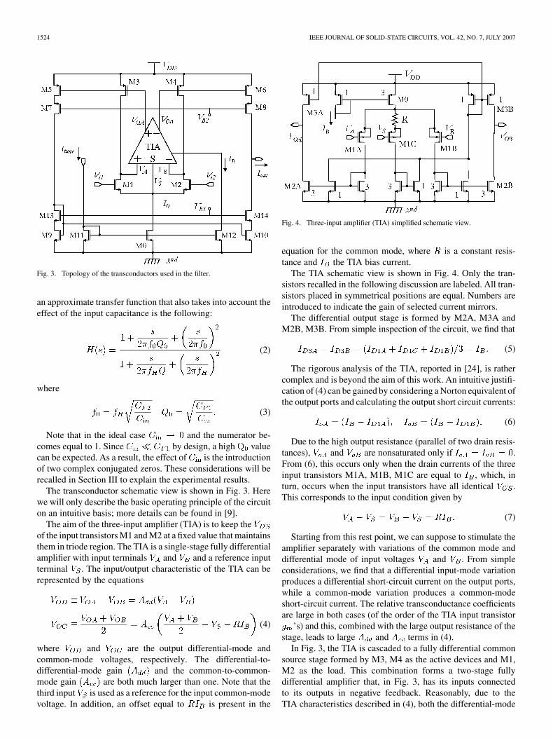
Fig. 3. Topology of the transconductors used in the filter.
an approximate transfer function that also takes into account theeffect of the input capacitance is the following:
(2)
where
(3)
Note that in the ideal case and the numerator be-comes equal to 1. Since by design, a high valuecan be expected. As a result, the effect of is the introductionof two complex conjugated zeros. These considerations will berecalled in Section III to explain the experimental results.
The transconductor schematic view is shown in Fig. 3. Herewe will only describe the basic operating principle of the circuiton an intuitive basis; more details can be found in [9].
The aim of the three-input amplifier (TIA) is to keep theof the input transistors M1 and M2 at a fixed value that maintainsthem in triode region. The TIA is a single-stage fully differentialamplifier with input terminals and and a reference inputterminal . The input/output characteristic of the TIA can berepresented by the equations
(4)
where and are the output differential-mode andcommon-mode voltages, respectively. The differential-to-differential-mode gain and the common-to-common-mode gain are both much larger than one. Note that thethird input is used as a reference for the input common-modevoltage. In addition, an offset equal to is present in the
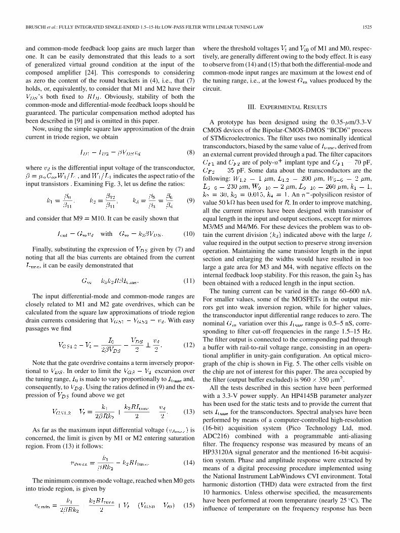
Fig. 4. Three-input amplifier (TIA) simplified schematic view.
equation for the common mode, where is a constant resis-tance and the TIA bias current.
The TIA schematic view is shown in Fig. 4. Only the tran-sistors recalled in the following discussion are labeled. All tran-sistors placed in symmetrical positions are equal. Numbers areintroduced to indicate the gain of selected current mirrors.
The differential output stage is formed by M2A, M3A andM2B, M3B. From simple inspection of the circuit, we find that
(5)
The rigorous analysis of the TIA, reported in [24], is rathercomplex and is beyond the aim of this work. An intuitive justifi-cation of (4) can be gained by considering a Norton equivalent ofthe output ports and calculating the output short circuit currents:
(6)
Due to the high output resistance (parallel of two drain resis-tances), and are nonsaturated only if .From (6), this occurs only when the drain currents of the threeinput transistors M1A, M1B, M1C are equal to , which, inturn, occurs when the input transistors have all identical .This corresponds to the input condition given by
(7)
Starting from this rest point, we can suppose to stimulate theamplifier separately with variations of the common mode anddifferential mode of input voltages and . From simpleconsiderations, we find that a differential input-mode variationproduces a differential short-circuit current on the output ports,while a common-mode variation produces a common-modeshort-circuit current. The relative transconductance coefficientsare large in both cases (of the order of the TIA input transistor
’s) and this, combined with the large output resistance of thestage, leads to large and terms in (4).
In Fig. 3, the TIA is cascaded to a fully differential commonsource stage formed by M3, M4 as the active devices and M1,M2 as the load. This combination forms a two-stage fullydifferential amplifier that, in Fig. 3, has its inputs connectedto its outputs in negative feedback. Reasonably, due to theTIA characteristics described in (4), both the differential-mode
BRUSCHI et al.: FULLY INTEGRATED SINGLE-ENDED 1.5–15-Hz LOW-PASS FILTER WITH LINEAR TUNING LAW 1525
and common-mode feedback loop gains are much larger thanone. It can be easily demonstrated that this leads to a sortof generalized virtual ground condition at the input of thecomposed amplifier [24]. This corresponds to consideringas zero the content of the round brackets in (4), i.e., that (7)holds, or, equivalently, to consider that M1 and M2 have their
’s both fixed to . Obviously, stability of both thecommon-mode and differential-mode feedback loops should beguaranteed. The particular compensation method adopted hasbeen described in [9] and is omitted in this paper.
Now, using the simple square law approximation of the draincurrent in triode region, we obtain
(8)
where is the differential input voltage of the transconductor,, and indicates the aspect ratio of the
input transistors . Examining Fig. 3, let us define the ratios:
(9)
and consider that M9 M10. It can be easily shown that
with (10)
Finally, substituting the expression of given by (7) andnoting that all the bias currents are obtained from the current
, it can be easily demonstrated that
(11)
The input differential-mode and common-mode ranges areclosely related to M1 and M2 gate overdrives, which can becalculated from the square law approximations of triode regiondrain currents considering that . With easypassages we find
(12)
Note that the gate overdrive contains a term inversely propor-tional to . In order to limit the excursion overthe tuning range, is made to vary proportionally to and,consequently, to . Using the ratios defined in (9) and the ex-pression of found above we get
(13)
As far as the maximum input differential voltage isconcerned, the limit is given by M1 or M2 entering saturationregion. From (13) it follows:
(14)
The minimum common-mode voltage, reached when M0 getsinto triode region, is given by
(15)
where the threshold voltages and of M1 and M0, respec-tively, are generally different owing to the body effect. It is easyto observe from (14) and (15) that both the differential-mode andcommon-mode input ranges are maximum at the lowest end ofthe tuning range, i.e., at the lowest values produced by thecircuit.
III. EXPERIMENTAL RESULTS
A prototype has been designed using the 0.35- m/3.3-VCMOS devices of the Bipolar-CMOS-DMOS “BCD6” processof STMicroelectronics. The filter uses two nominally identicaltransconductors, biased by the same value of , derived froman external current provided through a pad. The filter capacitors
and are of poly- implant type and pF,pF. Some data about the transconductors are the
following: m, m, m,m, m, m, ,
, , . An -polysilicon resistor ofvalue 50 has been used for . In order to improve matching,all the current mirrors have been designed with transistor ofequal length in the input and output sections, except for mirrorsM3/M5 and M4/M6. For these devices the problem was to ob-tain the current division indicated above with the largevalue required in the output section to preserve strong inversionoperation. Maintaining the same transistor length in the inputsection and enlarging the widths would have resulted in toolarge a gate area for M3 and M4, with negative effects on theinternal feedback loop stability. For this reason, the gain hasbeen obtained with a reduced length in the input section.
The tuning current can be varied in the range 60–600 nA.For smaller values, some of the MOSFETs in the output mir-rors get into weak inversion region, while for higher values,the transconductor input differential range reduces to zero. Thenominal variation over this range is 0.5–5 nS, corre-sponding to filter cut-off frequencies in the range 1.5–15 Hz.The filter output is connected to the corresponding pad througha buffer with rail-to-rail voltage range, consisting in an opera-tional amplifier in unity-gain configuration. An optical micro-graph of the chip is shown in Fig. 5. The other cells visible onthe chip are not of interest for this paper. The area occupied bythe filter (output buffer excluded) is 960 350 m .
All the tests described in this section have been performedwith a 3.3-V power supply. An HP4145B parameter analyzerhas been used for the static tests and to provide the current thatsets for the transconductors. Spectral analyses have beenperformed by means of a computer-controlled high-resolution(16-bit) acquisition system (Pico Technology Ltd, mod.ADC216) combined with a programmable anti-aliasingfilter. The frequency response was measured by means of anHP33120A signal generator and the mentioned 16-bit acquisi-tion system. Phase and amplitude response were extracted bymeans of a digital processing procedure implemented usingthe National Instrument LabWindows CVI environment. Totalharmonic distortion (THD) data were extracted from the first10 harmonics. Unless otherwise specified, the measurementshave been performed at room temperature (nearly 25 C). Theinfluence of temperature on the frequency response has been

1526 IEEE JOURNAL OF SOLID-STATE CIRCUITS, VOL. 42, NO. 7, JULY 2007
Fig. 5. Optical micrograph of the test chip.
Fig. 6. Static input–output characteristic measured at the two extremes of thetuning range.
characterized using a specially built Peltier cell cryostate with0.1 C precision.
Fig. 6 shows the static input–output characteristic for theupper and lower limits. A linear region slightly larger
than 2 V can be observed in both cases. For application insensor interfaces, it is important to examine the deviation fromthe ideal behavior . Considering the input voltageinterval 0.85–2.85 V, the deviation remains within 3 mVfor in the range 60–400 nA and progressively increasesbeyond this point. For 600 nA, the error varies from10 to 30 mV over the same input interval. The power supplycurrent varies from 50 to 500 A depending on tuning.
The amplitude and phase frequency response of the filter forthree values and 360-mV peak-to-peak (p-p) input signalis shown in Fig. 7. The input quiescent voltage was set to 2 V.Dashed lines represent the second-order ideal Butterworth low-pass functions having the same 3 dB frequency as the respec-tive experimental curves. The more significant differences fromthe ideal behavior are: 1) a sharp notch-like behavior nearlyone decade above , and 2) an asymptotic stop-band rejec-tion of nearly 45 dB. This behavior, observed also in electricalsimulations of the filter, is well explained by (2), representingthe effect of the transconductor input capacitances. Considering
Fig. 7. Amplitude and phase frequency response for three I values. Thedashed lines represent second-order low-pass fitting functions.
Fig. 8. Upper band limit (�3 dB) as a function of tuning current for three tem-peratures.
that the input capacitance comes entirely from the transcon-ductor triode region input transistors, can be approximatedby 0.25 resulting about 250 fF. Since ,is much greater than 1, as confirmed by the sharp notches in theamplitude response and steep phase inversion. The frequencyof the notch predicted by (3) is about 12 , in agreement withthe experimental results for from 60 to 300 nA, while alarge separation from is noticeable for 600 nA.The asymptotic stop-band rejection that can be derived from(2) and (3) is 43 dB, in good agreement with theexperiments.
The tuning law linearity predicted by (11) is maintainedover more than a decade, as proven by Fig. 8. Temperatureis expected to affect the OTA’s transconductance through thetemperature coefficients of the terms and in (11). The effecton the tuning law, clearly visible in Fig. 8, is a slope reductionof nearly 25% as the temperature varies from 0 to 80 C,which is to be ascribed mainly to the temperature coefficientof , as , according to nominal process data, exhibits a totalvariation less than 0.3% over the interval 0–80 C. Anotherpossible temperature-dependent term in (11) is the gain current
, deriving from the use of different transistor lengths in theinput and output sections. The shape of the curves is practically
BRUSCHI et al.: FULLY INTEGRATED SINGLE-ENDED 1.5–15-Hz LOW-PASS FILTER WITH LINEAR TUNING LAW 1527
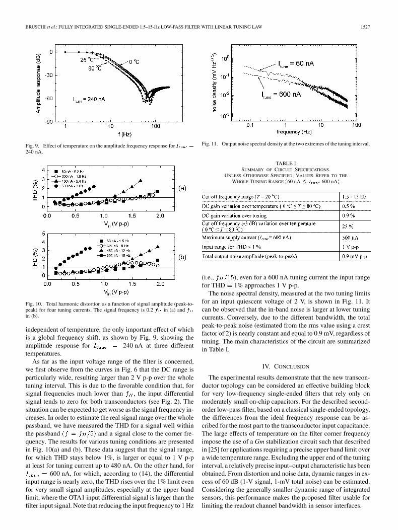
Fig. 9. Effect of temperature on the amplitude frequency response for I =240 nA.
Fig. 10. Total harmonic distortion as a function of signal amplitude (peak-to-peak) for four tuning currents. The signal frequency is 0.2 f in (a) and f
in (b).
independent of temperature, the only important effect of whichis a global frequency shift, as shown by Fig. 9, showing theamplitude response for 240 nA at three differenttemperatures.
As far as the input voltage range of the filter is concerned,we first observe from the curves in Fig. 6 that the DC range isparticularly wide, resulting larger than 2 V p-p over the wholetuning interval. This is due to the favorable condition that, forsignal frequencies much lower than , the input differentialsignal tends to zero for both transconductors (see Fig. 2). Thesituation can be expected to get worse as the signal frequency in-creases. In order to estimate the real signal range over the wholepassband, we have measured the THD for a signal well withinthe passband and a signal close to the corner fre-quency. The results for various tuning conditions are presentedin Fig. 10(a) and (b). These data suggest that the signal range,for which THD stays below 1%, is larger or equal to 1 V p-pat least for tuning current up to 480 nA. On the other hand, for
600 nA, for which, according to (14), the differentialinput range is nearly zero, the THD rises over the 1% limit evenfor very small signal amplitudes, especially at the upper bandlimit, where the OTA1 input differential signal is larger than thefilter input signal. Note that reducing the input frequency to 1 Hz
Fig. 11. Output noise spectral density at the two extremes of the tuning interval.
TABLE ISUMMARY OF CIRCUIT SPECIFICATIONS.
UNLESS OTHERWISE SPECIFIED, VALUES REFER TO THE
WHOLE TUNING RANGE (60 nA � I 600 nA)
(i.e., ), even for a 600 nA tuning current the input rangefor THD 1% approaches 1 V p-p.
The noise spectral density, measured at the two tuning limitsfor an input quiescent voltage of 2 V, is shown in Fig. 11. Itcan be observed that the in-band noise is larger at lower tuningcurrents. Conversely, due to the different bandwidth, the totalpeak-to-peak noise (estimated from the rms value using a crestfactor of 2) is nearly constant and equal to 0.9 mV, regardless oftuning. The main characteristics of the circuit are summarizedin Table I.
IV. CONCLUSION
The experimental results demonstrate that the new transcon-ductor topology can be considered an effective building blockfor very low-frequency single-ended filters that rely only onmoderately small on-chip capacitors. For the described second-order low-pass filter, based on a classical single-ended topology,the differences from the ideal frequency response can be as-cribed for the most part to the transconductor input capacitance.The large effects of temperature on the filter corner frequencyimpose the use of a Gm stabilization circuit such that describedin [25] for applications requiring a precise upper band limit overa wide temperature range. Excluding the upper end of the tuninginterval, a relatively precise input–output characteristic has beenobtained. From distortion and noise data, dynamic ranges in ex-cess of 60 dB (1-V signal, 1-mV total noise) can be estimated.Considering the generally smaller dynamic range of integratedsensors, this performance makes the proposed filter usable forlimiting the readout channel bandwidth in sensor interfaces.
1528 IEEE JOURNAL OF SOLID-STATE CIRCUITS, VOL. 42, NO. 7, JULY 2007
ACKNOWLEDGMENT
The authors wish to thank STMicroelectronics of Cornaredo(Milan, Italy) for fabricating the prototype chip.
REFERENCES
[1] Y. Papananos, T. Georgantas, and Y. Tsividis, “Design considerationsand implementation of very low frequency continuous-time CMOSmonolithic filters,” IEE Proc.-Circ. Devices Syst., vol. 144, pp. 68–74,1997.
[2] A. Veeravalli, E. Sanchez-Sinencio, and J. Silva-Martinez, “Transcon-ductance amplifier structures with very small transconductances: acomparative design approach,” IEEE J. Solid-State Circuits, vol. 37,no. 6, pp. 770–775, Jun. 2002.
[3] S. Solís-Bustos and J. Silva-Martinez, “A 4 Hz low-pass continuoustime filter,” in Proc. ICECS ’98, Lisboa, Portugal, Sep. 1998, vol. 1,pp. 169–172.
[4] M. Steyaert, P. Kinget, and W. Sansen, “Full integration of extremelylarge time constants in CMOS,” Electron. Lett., vol. 27, pp. 790–791,1991.
[5] A. Arnaud and C. Galup-Montoro, “Pico-A/V range CMOS transcon-ductors using series-parallel current division,” Electron. Lett., vol. 39,pp. 1295–1296, 2003.
[6] J. Silva-Martinez and J. S. Suñer, “Very low frequency IC filters,” inProc. 38th Midwest Symp. Circuits and Systems, Rio de Janeiro, Brazil,Aug. 1995, vol. 2, pp. 1325–1328.
[7] S. Solís-Bustos, J. Silva-Martinez, F. Maloberti, and E. S. Sánchez-Sinencio, “A 6-dB dynamic-range CMOS sixth-order 2.4-Hz low-passfilter for medical applications,” IEEE Trans. Circuits Syst. II, AnalogDigit. Signal Process., vol. 47, no. 12, pp. 1391–1398, Dec. 2000.
[8] R. Rieger, A. Demosthenous, and J. Taylor, “A 230-nW, 10-s time con-stant CMOS integrator for an adaptive nerve signal amplifier,” IEEE J.Solid-State Circuits, vol. 39, no. 11, pp. 1968–1975, Nov. 2004.
[9] P. Bruschi, F. Sebastiano, N. Nizza, and M. Piotto, “A tunable CMOStransconductor for ultra-low Gm with wide differential input voltagerange,” in Proc. ECCTD ’05, Cork, Ireland, Sep. 2005, vol. 3, pp.337–340.
[10] D. Johns and K. Martin, Analog Integrated Circuits Design. NewYork: Wiley, 1996, ch. 15.
[11] C. C. Hung, K. A. I. Halonen, and M. Ismail, “A low-voltage,low-power CMOS fifth-order elliptic GM-C filter for basebandmobile, wireless communication,” IEEE Trans. Circuits Syst. VideoTechnol., vol. 7, no. 4, pp. 584–593, Aug. 1997.
[12] G. Duzenli, Y. Kilic, H. Kuntman, and A. Ataman, “On the design oflow-frequency filters using CMOS OTAs operating in the subthresholdregion,” Microelectron. J., vol. 30, pp. 45–54, 1999.
[13] O. Omeni, E. Rodríguez-Villegas, and C. Toumazou, “A micropowerCMOS continuous-time filter with on-chip automatic tuning,” IEEETrans. Circuits Syst. I, Fundam. Theory Applicat., vol. 52, no. 4, pp.695–705, Apr. 2005.
[14] A. El Mourabit, G. N. Lu, and P. Pittet, “A low frequency, sub-1.5 V mi-cropower Gm-C filter based on subthreshold MIFG MOS transistors,”in Proc. ESSCIRC ’05, Grenoble, France, Sep. 2005, pp. 331–334.
[15] E. Rodriguez-Villegas, “A 0.8 V, 360 nW Gm-C biquad based onFGMOS transistors,” in Proc. ISCAS ’05, Kobe, Japan, May 2005,vol. 3, pp. 2156–2159.
[16] U. Yodprasit and J. Ngarmnil, “Micropower transconductor forvery-low frequency filters,” in Proc. IEEE Asia-Pacific Conf. SolidState Circuits (APCCAS), Chiangmai, Thailand, Nov. 1998, pp. 5–8.
[17] C. C. Hung, K. Halonen, V. Porra, and M. Ismail, “Low-voltage, mi-cropower, weak inversion CMOS Gm-C filters,” in Proc. ICEC ’96,Rodos, Greece, Oct. 1996, vol. 2, pp. 1178–1181.
[18] A. Arnaud and C. Galup-Montoro, “A fully integrated 0.5–7 HzCMOS bandpass amplifier,” in Proc. ISCAS ’04, Vancouver, Canada,May 2004, vol. 1, pp. 445–448.
[19] A. Veeravalli, E. Sanchez-Sinencio, and J. Silva-Martinez, “A CMOStransconductance amplifier architecture with wide tuning range forvery low frequency applications,” IEEE J. Solid-State Circuits, vol.37, no. 6, pp. 776–781, Jun. 2002.
[20] R. Castello, F. Montecchi, F. Rezzi, and A. Baschirotto, “Low-voltageanalog filters,” IEEE Trans. Circuits Syst. I, Fundam. Theory Applicat.,vol. 42, no. 11, pp. 827–840, Nov. 1995.
[21] J. A. De Lima and W. A. Serdijn, “Compact nA/V triode-MOSFETtransconductor,” Electron. Lett., vol. 41, pp. 1113–1114, 2005.
[22] U. Gatti, F. Maloberti, G. Palmisano, and G. Torelli, “CMOS triode-transistor transconductor for high-frequency continuous-time filters,”IEE Proc.-Circ. Devices Syst., vol. 141, pp. 462–467, 1994.
[23] T. Deliyannis, Y. Sun, and J. K. Fidler, Continuous-Time Active FilterDesign. Boca Raton, FL: CRC Press, p. 280.
[24] P. Bruschi, F. Sebastiano, and N. Nizza, “CMOS transconductors withnearly constant input ranges over wide tuning intervals,” IEEE Trans.Circuits Syst. II, Exp. Briefs, vol. 53, no. 10, pp. 1002–1006, Oct. 2006.
[25] P. Bruschi, G. Barillaro, F. Pieri, and M. Piotto, “Temperature sta-bilised tunable Gm-C filter for very low frequencies,” in Proc. ESS-CIRC ’04, Leuven, Belgium, Sep. 2004, pp. 107–110.
Paolo Bruschi was born in Massa, Italy, in 1964. Hereceived the Laurea degree in electronic engineeringfrom the University of Pisa, Italy, in 1989.
In 1993, he joined the Department of InformationEngineering as a Researcher. He is currently an Asso-ciate Professor in the Department of Information En-gineering of the University of Pisa. His main area ofinterest is the development of integrated silicon sen-sors and actuators. He is also involved in the designof analog integrated circuits and the development ofprocess simulators.
Nicolò Nizza received the Laurea degree (cum laude)in electronic engineering from the University of Pisa,Italy, in 2004. He is currently working toward thePh.D. degree in electronic engineering at the sameuniversity.
His main research interests are in analog andmixed-signal integrated circuit design and integratedsensor interfaces.
Francesco Pieri received the Laurea and the Ph.D.degree in electrical engineering, both from the Uni-versity of Pisa, Italy, in 1996 and 2000, respectively.
He joined the Department of Information En-gineering of the same university as a Researcherin 2001. His current research interests includeapplications of porous silicon to sensors andmicrotechnologies, and development of microelec-tromechanical systems.
Monica Schipani received the Laurea degree inelectronic engineering from the University of Pisa,Italy, in 2004. She currently is a Ph.D. candidate atthe Department of Information Engineering of theUniversity of Pisa, carrying out research on sensorinterfaces in cooperation with STMicroelectronicsof Cornaredo, Milan, Italy.
Danilo Cardisciani received the Laurea and theLaurea Specialistica degrees in electronic engi-neering from the University of Pisa, Italy, in July2003 and May 2006, respectively.
Since September 2006, he has been working as anAnalogue/RF IC Design Engineer for Cambridge Sil-icon Radio Ltd (CSR) where he is involved in thedevelopment of Bluetooth transceivers in submicro-metric CMOS technology.